optik an grenzfl¨achen und nanostrukturen - uni-potsdam.de · optik an grenzfl¨achen und...
TRANSCRIPT

Optik an Grenzflachen und Nanostrukturen Sommersemester 2017Carsten Henkel
Ubungsblatt 4 Ausgabe: Di 06. Jun 17Eingabe: Do 15. Juni 17
Aufgabe 4.1 – Surface plasmon dispersion (10 Punkte)
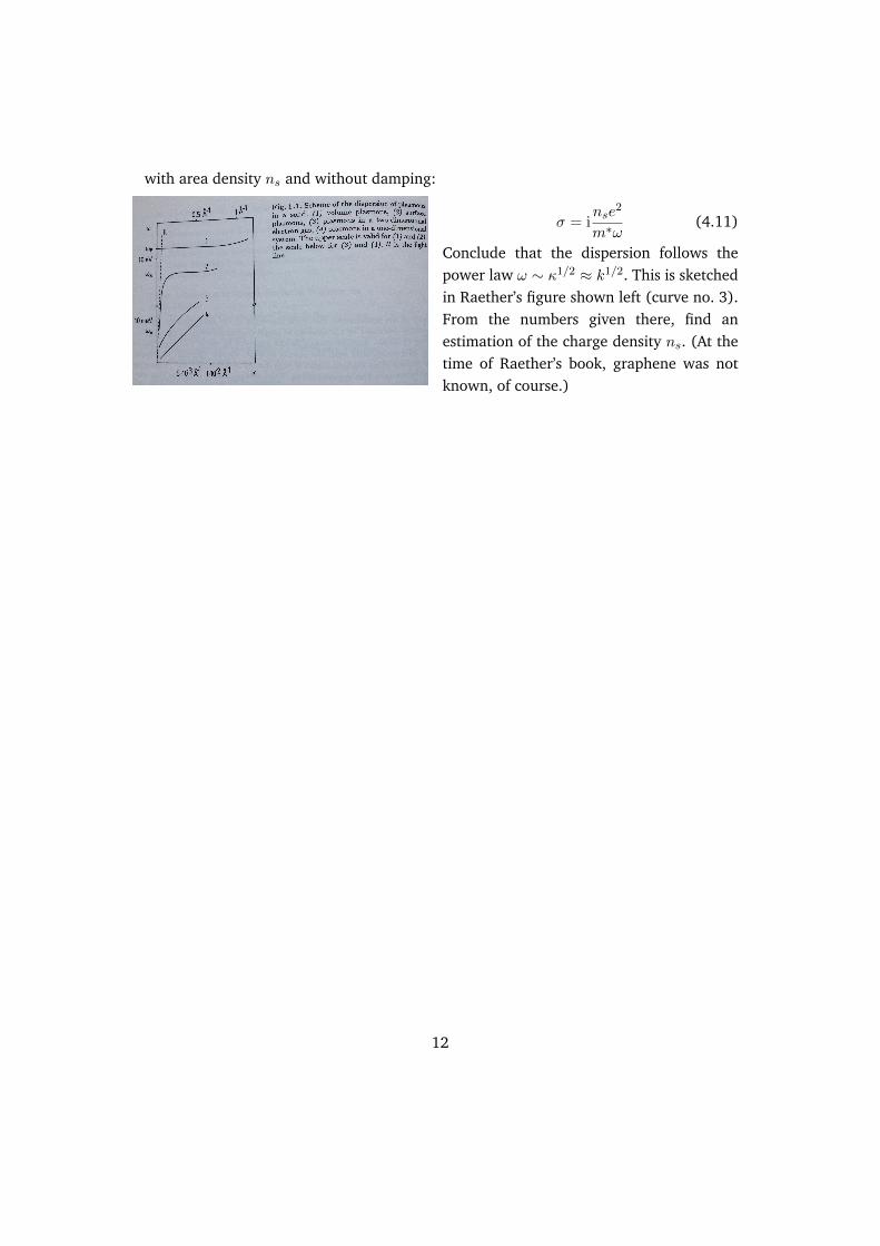
In Raether’s book on surface plasmons,you can find this Figure, showing schema-tically the dispersion relation !(k). Theup-bending at large k is the topic of thisexercise.
(i) Compare the surface plasmon wa-velength (parallel to the surface) wherethe up-bending appears, to the plasmawavelength �
p
= 2⇡/kp
= 2⇡c/!p
andspeculate why this effect is often attributedto ‘microscopic physics’.
(ii) Since the plasmon dispersion appears for large k (small scales), let us try a sim-plified description where retardation is neglected. The light field is described by theelectric potential �(r) alone (no vector potential). If this potential varies like e
ik
x
x�(z)
outside the metal (i.e., in the region z � 0), show that �(z) ⇠ e
�|kx
|z. Similarly, you mayassume that �(z) ⇠ e
|kx
|z inside the metal (z 0).(iii) Start with the Ansatz for the potential
�(x, z) =
(�0
e
ik
x
x
e
�|kx
|z z � 0
�m
e
ik
x
x
e
|kx
|z z 0
(4.1)
and show that the continuity of � and of "Ez
gives the following dispersion equation forthe surface plasmon:
k"0
= �k"m
, k = |kx
| (4.2)
or ! = !p
/p2 for a Drude metallic dielectric function (no losses, no background polari-
sation).(iv) On short scales, the electric charge density at a metallic surface may also oscillate
in such a way that a surface polarisation Ps
is built up. This corresponds to an areadensity of dipole moments (oriented perpendicular to the surface, in other fields alsoknown as ‘double layer’). By analogy to a parallel-plate capacitor (Plattenkondensator),
8

such a surface polarisation translates into a ‘jump condition’ for the electric potential:
lim
z&0
�(z) = lim
z%0
�(z) +Ps
"0
(4.3)
where the limits are understood as ‘coming from outside the metal’ and ‘coming frominside the metal’ (while points within the surface polarization are ‘forbidden’). Make asketch of the electric potential. Show that we get the system of equations for the surfaceplasmon:
�0
= �m
+
Ps
"0
, k"0
�0
= �k"m
�m
(4.4)
(v) To solve these equations, we need a relation between the surface polarisation andthe electric field. The simplest local Ansatz is a linear response to the ‘inner field’
Ps
= "0
↵ lim
z%0
Ez
(4.5)
with a complex coefficient ↵, the so-called ‘surface polarisability’. Check that ↵ has thedimensions of a length: since Feibelman’s work [Phys. Rev. B 40 (1989) 2752], it isinterpreted as the ‘centroid’ (Schwerpunkt) of the electronic charge density of the me-tallic surface. Show that in terms of ↵, one gets with a lossless Drude model for "
m
thedispersion relation
!sp
(k) ⇡ !pp
2� k↵(4.6)
One typically considers that this simple model is only meaningful when ↵ is small: ex-pand the dispersion relation and estimate the group velocity @!
sp
/@k for the surfaceplasmon.
Aufgabe 4.2 – Graphene plasmons (10 Punkte)
Graphene is a two-dimensional material made from a one-atom thick layer of carbonatoms, arranged in a honeycomb lattice. Because of delocalised electronic states, it has avery high in-plane conductivity � = J/Ek where J is the surface current density and Ekthe in-plane electric field. We construct in this problem a surface plasmon whose field ispeaking right in the graphene plane (located at z = 0).
(i) For a free standing graphene film, consider a magnetic field (all fields oscillate⇠ e
�i!t, H(+0) = lim
z&0
H(z))
Hy
(x, z) =
8<
:H(+0) e
ik
x
x�z , z > 0
H(�0) e
ik
x
x+z , z < 0
(4.7)
and show that its jump at z = 0 is proportional to the surface current density
H(+0) e
ik
x
x �H(�0) e
ik
x
x
= �Jx
(4.8)
9

Solution. In the Ampere–Maxwell equation
r⇥H = j+ @t
D ,
we need the (‘external’) current density to fix the jump in the magnetic field. (This is similar to thejump in the normal electric field in r ·D = ⇢ when a surface charge is present.) A geometric argument
is based on Stokes’ theorem and a small area �a = �y�z that is ‘pierced’ by the graphene sheet.The area normal is along the x-direction, parallel to the surface current J. The integral over r⇥H istransformed into a closed line integral
Z(r⇥H) · da =
IH · ds ⇡ [�H
y
(+0) +Hy
(�0)]�y
where in the last expression, the limit �z ! 0 was taken. The integral over the current density j givesin the same limit the sheet current Z
j · da = Jx
�y
(because this current is localised, like a �-function in the interior of the area). Finally, for the displace-ment current @
t
D, Z@t
D · da = @t
D�y�z
we argue that @t
D is bounded so that the average value theorem can be applied. (After all, D iscontinuous across the graphene sheet.) As a result, this last integral vanishes in the limit �z ! 0, andwe get
�Hy
(x, y,+0) +Hy
(x, y,�0) = Jx
which is Eq.(4.8).
(ii) Evaluating the Ampere-Maxwell equation outside the film, compute the tangen-tial electric field
Ex
(x, z) =
8>>><
>>>:
iH(+0)
!"0
e
ik
x
x�z , z > 0
� iH(�0)
!"0
e
ik
x
x+z , z < 0
(4.9)
Since this field is continuous across the film, we can conclude that H(�0) = �H(+0).Make a sketch of the magnetic and electric fields.
(iii) By using Ohm’s law for the surface current Jx
, find the dispersion relation
! = � i�
2"0
(4.10)
For a surface plasmon with weak damping, we thus need an imaginary conductivity.The simplest model is to describe the graphene electrons as a two-dimensional ideal gas
10
with area density ns
and without damping:
� = i
ns
e2
m⇤!(4.11)
Conclude that the dispersion follows thepower law ! ⇠ 1/2 ⇡ k1/2. This is sketchedin Raether’s figure shown left (curve no. 3).From the numbers given there, find anestimation of the charge density n
s
. (At thetime of Raether’s book, graphene was notknown, of course.)
12