optically addressed modulator for tunable spatial
TRANSCRIPT
Mathematisch-Naturwissenschaftliche Fakultät
Frederik Schaal | Michael Rutloh | Susanne Weidenfeld | Joachim Stumpe | Peter Michler | Christof Pruss | Wolfgang Osten
Optically addressed modulator for tunable spatial polarization control
Postprint archived at the Institutional Repository of the Potsdam University in:Postprints der Universität PotsdamMathematisch-Naturwissenschaftliche Reihe ; 1001ISSN 1866-8372https://nbn-resolving.org/urn:nbn:de:kobv:517-opus4-446263DOI https://doi.org/10.25932/publishup-44626
Suggested citation referring to the original publication:Optics Express 26 (2018) 21, pp. 28119-28130 DOI https://doi.org/10.1364/OE.26.028119ISSN (online) 1094-4087

Optically addressed modulator for tunablespatial polarization controlFREDERIK SCHAAL,1 MICHAEL RUTLOH,2 SUSANNE WEIDENFELD,3
JOACHIM STUMPE,2 PETER MICHLER,3 CHRISTOF PRUSS,1,* ANDWOLFGANG OSTEN1
1Institut für Technische Optik, Universität Stuttgart, Pfaffenwaldring 9, Stuttgart, D-70569, Germany2Universität Potsdam, Karl-Liebknecht Straße 24/25, Potsdam, D-14476, Germany3Institut für Halbleiteroptik und Funktionelle Grenzflächen, Universität Stuttgart, Allmandring 3, Stuttgart,D-70569, Germany*[email protected]
Abstract: We present an optically addressed non-pixelated spatial light modulator. The systemis based on reversible photoalignment of a LC cell using a red light sensitive novel azobenzenephotoalignment layer. It is an electrode-free device that manipulates the liquid crystal orientationand consequently the polarization via light without artifacts caused by electrodes. The capabilityto miniaturize the spatial light modulator allows the integration into a microscope objective.This includes a miniaturized 200 channel optical addressing system based on a VCSEL arrayand hybrid refractive-diffractive beam shapers. As an application example, the utilization as amicroscope objective integrated analog phase contrast modulator is shown.© 2018 Optical Society of America under the terms of the OSA Open Access Publishing Agreement
OCIS codes: (230.6120) Spatial light modulators; (230.3720) Liquid-crystal devices; (050.1970) Diffractive optics;(160.5335) Photosensitive materials; (160.1190) Anisotropic optical materials; (130.3990) Micro-optical devices.
References and links1. G. Lazarev, A. Hermerschmidt, S. Krüger and S. Osten, “LCOS spatial light modulators: trends and applications,” in
Optical Imaging and Metrology: Advanced Technologies, W. Osten and N. Reingand, eds. (Wiley-VCH, 2012), pp.1–23.
2. Z. Zhang, Z. You, and D. Chu, “Fundamentals of phase-only liquid crystal on silicon (LCOS) devices,” Light Sci.Appl. 3(10), e213 (2014).
3. C. Lingel, T. Haist, and W. Osten, “Optimizing the diffraction efficiency of SLM-based holography with respect tothe fringing field effect,” Appl. Opt. 52(28), 6877–6883 (2013).
4. N. Collings, S. Mias, T. Wilkinson, A. Travis, J. Moore, and W. Crossland, “Optically addressed spatial lightmodulator performance and applications,” Proc. SPIE 5213, 40–48 (2003).
5. P. Shrestha, Y. Chun, and D. Chu, “A high-resolution optically addressed spatial light modulator based on ZnOnanoparticles,” Light Sci. Appl. 4(3), e259 (2015).
6. U. Efron, J. Grinberg, P. O. Braatz, M. J. Little, P. G. Reif, and R. N. Schwartz, “The silicon liquid-crystal lightvalve,” J. Appl. Phys. 57(4), 1356–1368 (1985).
7. D. Armitage, W. Anderson, and T. Karr, “High-speed spatial light modulator,” IEEE J. Quantum Electron. 21(8),1241–1248 (1985).
8. A. Natansohn and P. Rochon, "Photoinduced Motions in Azo-Containing Polymers," Chem. Rev. 102, 4139–4176(2002).
9. L. Angiolini, "Smart Light-Responsive Materials: Azobenzene-Containing Polymers and Liquid Crystals," Macromol.Chem. Phys. 211, 481 (2010).
10. A. V Bogdanov and A. K. Vorobiev, "ESR and Optical Study of Photo-Orientation in Azobenzene-ContainingLiquid-Crystalline Polymer," J. Phys. Chem. B 117, 12328–12338 (2013).
11. K. Ichimura, Y. Suzuki, T. Seki, A. Hosoki, and K. Aoki, "Reversible change in alignment mode of nematic liquidcrystals regulated photochemically by command surfaces modified with an azobenzene monolayer," Langmuir 4(1),1214–1216 (1988).
12. T. Seki, M. Sakuragi, Y. Kawanishi, T. Tamaki, R. Fukuda, K. Ichimura, and Y. Suzuki, "Command surfaces ofLangmuir-Blodgett films. Photoregulations of liquid crystal alignment by molecularly tailored surface azobenzenelayers," Langmuir 9(1), 211–218 (1993).
13. S. Furumi and K. Ichimura, "Photogeneration of High Pretilt Angles of Nematic Liquid Crystals by Non-PolarizedLight Irradiation of Azobenzene-Containing Polymer Films," Adv. Funct. Mater. 14, 247–254 (2004).
Vol. 26, No. 21 | 15 Oct 2018 | OPTICS EXPRESS 28119
#335477 https://doi.org/10.1364/OE.26.028119 Journal © 2018 Received 5 Jul 2018; revised 15 Aug 2018; accepted 17 Aug 2018; published 12 Oct 2018

14. W. M. Gibbons, P. J. Shannon, S.-T. Sun, and B. J. Swetlin, "Surface-mediated alignment of nematic liquid crystalswith polarized laser light," Nature 351, 49–50 (1991).
15. V. G. Chigrinov, V. M. Kozenkov, and H.-S. Kwok, "Photoalignment of LCs," in Photoalignment of Liquid CrystallineMaterials (John Wiley & Sons, Ltd, 2008), pp. 69–100.
16. M. Eichfelder, W.-M. Schulz, M. Reischle, M. Wiesner, R. Roßbach, M. Jetter, and P. Michler, "Room-temperaturelasing of electrically pumped red-emitting InP/(Al0.20Ga0.80)0.51In0.49P quantum dots embedded in a verticalmicrocavity," Appl. Phys. Lett. 95, 131107 (2009).
17. F. Gallego-Gomez, F. del Monte, and K. Meerholz, "Optical gain by a simple photoisomerization process," Nat.Mater. 7, 490–497 (2008).
18. N. Otsuki, N. Fujioka, N. Kawatsuki, and H. Ono, "Photoinduced Orientation and Holographic Recording in PolyesterFilms Comprising Azobenzene Side-Groups Using 633 nm Red Light," Mol. Cryst. Liq. Cryst. 458(1), 139–148(2006).
19. D. S. Correa, M. R. Cardoso, V. C. Goncalves, D. T. Balogh, L. De Boni, and C. R. Mendonca, "Optical birefringenceinduced by two-photon absorption in polythiophene bearing an azochromophore," Polymer 49(6), 1562–1566 (2008).
20. C. R. Mendonca, U. M. Neves, L. De Boni, A. A. Andrade, D. S. dos Santos Jr., F. J. Pavinatto, S. C. Zilio, L.Misoguti, and O. N. Oliveira Jr., "Two-photon induced anisotropy in PMMA film doped with Disperse Red 13," Opt.Commun. 273, 435–440 (2007).
21. J. Stumpe, O. Sakhno, Y. Gritsai, R. Rosenhauer, T. Fischer, M. Rutloh, F. Schaal, S. Weidenfeld, M. Jetter, P. Michler,and others, "Active and Passive LC Based Polarization Elements," Mol. Cryst. Liq. Cryst. 594(1), 140–149 (2014).
22. F. Schaal, M. Rutloh, S. Weidenfeld, J. Stumpe, and W. Osten, "Tunable non-pixelated spatial polarization shapingincluding an integrated optical addressing unit," Proc. SPIE 9181, 91810H (2014).
23. F. Schaal, M. Rutloh, S. Weidenfeld, J. Stumpe, M. Jetter, P. Michler, and W. Osten, "Polarization Elements,"’ inTunable Micro-Optics, H. Zappe and C. Duppe, eds. (Cambridge University Press, 2015).
24. M. Warber, S. Zwick, M. Hasler, T. Haist, and W. Osten, "SLM-based phase-contrast filtering for single and multipleimage acquisition," Proc. SPIE 7442, 74420E (2009).
25. A. Marquez, I. Moreno, C. Iemmi, A. Lizana, J. Campos, and M. J. Yzuel, "Mueller-Stokes characterization andoptimization of a liquid crystal on silicon display showing depolarization," Opt. Express 16(3), 1669–1685 (2008).
26. E. A. Shteyner, A. K. Srivastava, V. G. Chigrinov, H.-S. Kwok, and A. D. Afanasyev, "Submicron-scale liquid crystalphoto-alignment," Soft Matter 9, 5160–5165 (2013).
1. Introduction
Reversible spatial polarization shaping devices are widely used in optical systems. They are eitherutilized to manipulate polarization properties or used to generate spatial phase or amplitudemodulation. Examples for their application include dynamic beam shaping/splitting/steering,optical tweezers, pattern generation, information storage, optical processing, or holography.
Currently the most common technology for this purpose are electrically addressed spatial lightmodulators (SLM). Their working principle is based on the re-orientation of liquid crystals (LC)using pixelized electrodes. Those can be configured for transmission or reflection use. SLMdevices can consist of several millions of pixels with sizes down to 3 µm and are available ascommercial products [1, 2].
Benefits of SLM systems are the high amount of individually addressable pixels and the easycontrol by digital electrical interfaces. The drawback of those devices is the limited spatialresolution, crosstalk between neighbouring pixels, spurious diffraction orders and efficiencylosses due to the electrode structure and pixelation [3].Optically addressed spatial light modulators (OASLM) are based on optically addressed
photoconductor layer. In combination with transparent electrodes and voltage sources, they causethe reorientation of a liquid crystal layer [4, 6, 7].
OASLMs have no pixelation and can be fabricated in large areas and high spatial resolutions [5].But they need an external high-voltage supply and an external optical addressing system. Theaddressing principle is based on the same effect as SLMs (LC orientation by electrical fields,optical anisotropy caused by birefringence), but the voltage between the electrodes is alteredthrough photoconductors and not by electronic means.In order to simplify the system, avoid negative effects from electrodes (e.g. crosstalk or
pixelation), and enable all optical systems, the tuning of birefringence via light would beadvantageous.
Vol. 26, No. 21 | 15 Oct 2018 | OPTICS EXPRESS 28120

The induction of anisotropy due to photo-orientation or photo-selection in polymer films uponexposure with polarized light [8] is used for the fabrication of static photoalignment layers andpermanent polarisation elements. But for long-term and high cycle numbers, hysteresis andreversibility, switching times and durability are insufficient for applicable devices, with regardsto the influence of the solid state matrix [9, 10].
A solution for these issues is the reversible photoalignment of liquid crystals with an azobenzene-containing optically addressed monolayer [11] (see also section 3.1). This enables the fast,reversible, wearless and reproducable optical induction of birefringence. Usually, the polarizedlight used for addressing is in the range between 366-532 nm with respect to the absorbance ofconventional azobenzenes [12–15].The usage of a photo-addressable light modulator also depends on the addressing system -
mainly regarding wavelength, polarization and power density of the addressing pattern. Complexand compact micro-optical addressing systems need high-density switchable light sources, e.g.vertical-cavity surface-emitting lasers (VCSEL). But so far, such stable light sources are onlyavailable at wavelengths of >640 nm [16].
Currently the main disadvantages of electrically addressed SLMs are aberrations due to SLMunevenness, spurious diffraction orders, stray light generation and spatial resolution. Opticallyaddressed modulators can overcome these limitations, but their application requires an opticaladdressing system. Optical addressing systems are voluminous and require often an additionalSLM for pattern generation. VCSEL arrays and micro-optical components are enablers forcompact multi-channel optical addressing systems. In contrast to edge emitters, VCSEL canbe fabricated in precise positioned arrays. They emit linearly polarized light with is needed foroptical addressing. But there are no fast (switching time <100 s [18]) and stable materials forreversible optical addressing at stable VCSEL emission wavelengths. The material development,especially with respect to the switching time, gets more and more challenging with increasingwavelengths, due to the energy of the addressing light. Therefore it is necessary to develop newfast optical addressable materials to obtain the benefits of compact optical addressing systemsbased on red light VCSEL arrays.
Here, we present the properties of a new red light photo-addressable cell in combination witha compact optical addressing module. The applications and benefits of such a system comparedto SLMs are demonstrated by a tunable microscope objective integrated phase contrast device.
2. System design and principle of operation
The purpose of the system is to generate spatial reversible tunable birefringence patterns(spatial light modulator). It allows for the manipulation of polarization, phase or amplitude oftransmitting light fields. The principle of operation (Fig. 1) is based on the optical addressing ofa photo-addressable cell (PAC).The desired spatial addressing pattern is projected into the photoaligning layer of the PAC.
Depending on the intensity of the addressing light the degree of birefringence is spatially altered inthe PAC plane. Linearly polarized light with wavelengths 640-660 nm is used for addressing. Theresulting birefringence pattern can be used with NIR and SWIR light (900-1800 nm wavelength).But visible light of low power density (< 10 mW/cm2) is applicable too.The main components of the optical addressing system are a VCSEL array as light source,
diffractive optical elements and an axicon for beam-shaping. The optically induced birefingenceis generated in the photoaddressable cell.
Vol. 26, No. 21 | 15 Oct 2018 | OPTICS EXPRESS 28121

1
Optical addressing
Photo addressable cell
Modified light field
Incoming light field
Optical induced birefringence
Fig. 1. Schematic of the optical addressed spatial polarization shaping system.
3. System components
3.1. Photoaddressable cell
The PAC (Fig. 2(a) ) is formed by two glass substrates. The inner surface of the first substrateis covered with an azobenzene-containing optically addressable monolayer of 10 nm thicknessachieving a reversible LC photoalignment, whereas the second substrate is covered with a rubbedpolyimide film of 50nm thickness causing a permanent planar LC alignment. The thickness ofthe complete PAC is controlled by precise spacers based on microspheres (10 µm thickness). Dueto the monomolecular addressing layer and the transparency of the LC mixture, the transmissionof the assembled cell (Fig. 2(b) ) is dominated by Fresnel losses.
So far, photoisomerisation and photo-orientation processes of azobenzenes are mainly reportedusing green, blue or UV light, according to the absorbance of conventional azobenzenes. Only afew publications have reported on the induction of anisotropy using red light mainly up to 633nm [17–20]. Especially the reversibility and switching times (>100 s) of the used photosensitivepolymeric azobenzene materials are too slow for technical applications.
Therefore, it was necessary to develop a new photo-addressable material with faster switchingtime, long lifetime and excellent reversibility. Based on our previous work, [21–23] the newphoto-addressable material Silan IV (Fig. 2(c) ) improves the switching time of the red addressablematerial.
The photo-addressable terminal substituted bis-azobenzene containing triethoxy silane (SilanIV) is covalently linked to the surface of one of the glass substrates (soda-lime-silica glass of 1mm thickness). In order to control the interaction between neighbouring molecules and to ensurethe reversibility of the optical addressing, the Silan IV monolayer is formed by self-assemblingand proper post-treatment by rinsing with toluene.In the initial state, the photosensitive aligning layer causes a homeotropic alignment of the
nematic LC mixture E5 (Merck, Darmstadt). In combination with the planar alignment caused bythe rubbed PI layer of the second substrate, it results in a splay orientation of the initial LC cell(Fig. 3(b) ).
The exposure with polarized red light changes the splay orientation of the LC cell to a planarone (Fig. 3(a) ). The related change of the optical properties of the LC cell is caused by two effects.Firstly, the photoisomerisation of the push-pull-substituted bis-azobenzene moieties changesthe molecular shape of the initial rod-like EE isomer to the crooked EZ isomer. A steady statebetween both isomeric forms is established. The related modification of the monolayer causes
Vol. 26, No. 21 | 15 Oct 2018 | OPTICS EXPRESS 28122

a change of the boundary condition resulting in a planar LC orientation, changing the splay toplanar order of the cell.
glass substrate
optical addressed layer (~10 nm)
nematic liquid crystal (1-10 µm)
static orientation layer (~50 nm)
glass substrate
a) b)
c)
Fig. 2. a) Composition of the photo-addressable cell (PAC); b) Image of a PAC; c) Molecularstructure of the initial material of the photo-addressable command layer: Silan IV withterminal attached push-pull bis triethoxy-bis-azobenzene.
By Switching off the addressing light, the azobenzene relaxes thermally back on molecularlevel to the rod-like EE isomer in some ms. This results in the re-establishing of the homeotropicorientation of the EE bis-azobenzene monolayer and the related relaxation of the LC moleculesclose to this substrate, establishing the initial splay order of the cell again in 30 seconds. Such a"command surface effect" was already demonstrated by Ichimura in 1988, using monolayers withconventional azobenzenes and the exposure with UV and visible light [11].
Secondly, upon continued exposure with linear polarized red light the bis-azobenzene moietiesundergo angle selective absorbance and corresponding EE/EZ photoisomerization cycles, depend-ing on the angle between the transition dipole moment of the azobenzene unit and the electricfield vector of the incident light. The polarized irradiation tends to orientate the chromophoresperpendicular to the electric field vector of the linear polarized light in the steady state of thephotoisomerization. Subsequently, the photochromic groups become orientated perpendicularto the electric field vector of the incident light, enriching the azobenzenes perpendicular to theelectric field vector (which was perpendicular to the rubbing direction of the PI aligning layer).In this way, the planar order is being improved during irradiation.Due to the low thickness of the monocular addressing layer, (< 10 nm) the induced optical
path difference change of Silan IV monolayer is extremely small. Therefore, the change ofphoto-induced birefringence is amplified by the alignment of the whole LC bulk layer.
The temporal response (Fig. 4(a) ) of the optical addressing is initiated by optically addressingthe cell with linear polarized red laser light (wavelength 660 nm, power density 500 mW/cm2).The birefringence change is measured with a fast (using photoacoustic modulators) ellipsometer(Horiba Jobin Yvon UVISEL). The change of birefringence (B(t)) is fitted to a first-orderexponential decay function (B(t) = A · exp(−t/tc) + B0). The value t95 = 3 · tc is used forcharacterizing the response time. The parameter t95 describes the time necessary to obtain 95 %of the birefringence limit value. For the cell with Silan IV addressing layers, a response time oft95 of 4,1 ±0, 15 s was reached at a power density of 500 mW/cm2. This is significantly fasterthan previously known red light addressable materials (>100 s [18]), but still considerably slowerthan SLMs (≈0,01 s [2]).
Vol. 26, No. 21 | 15 Oct 2018 | OPTICS EXPRESS 28123

a) b)
Fig. 3. a) Schematic illustration of planar orientation of liquid crystal molecules; b) Schematicillustration of splay orientation of liquid crystal molecules.
The switching time depends on the power of the addressing light. At a power density of100 mW/cm2, which corresponds to that of the 200 channel optical addressing system, theswitching time drops to t95 = 6,5 s (Fig. 4(d) ).After turning off the addressing light, the orientation of the LC layer relaxes thermally back
(Fig. 4(b) ) with a time constant of t95 = 34 s (at 22oC temperature). The maximum birefringencechange generated is ∆n = 0,19 for 10 µm LC thickness. The reversibility of the system is very high.After 22000 cycles of optical addressing, (500 mW/cm2, 660 nm) no change in the birefringencehub was detected.The investigation was carried out with the terminal attached bis-azobenzene, as shown in
Fig. 2. In this case, the silane group is attached via a spacer to the p-methyl, alkyl-amino group.But the experiments were continued using a lateral attached p-dimethylamino bis-azobenzene.Upon red light exposure the initial splay configuration is transformed to a planar aligned LC-cellas well. But in contrast to the terminal attached azobenzene, the thermal back isomerization tothe EE isomer does not result into the initial splay cell, switching off the light. As expected, thelateral attached bis-azobenzene has a much higher tendency for planar alignment in contrast tothe terminal substituted bis-azobenzene. The continued exposure with an ammended polarizationdirection, with respect to the rubbing direction, causes a change of the aligning direction. As aconsequence, the planar cell is changed to a twisted planar aligned cell. This allows a continuouschange of the birefringence (Fig. 4(c) ). The nonlinear response of the PAC is very stable and canbe compensated by a look up table in the control system. The resulting birefringence deviationsare mainly introduced by fluctuations of the light source. In our setup (VCSEL light powerstability 0.5 %) birefringence resolutions of 6.9 · 10−4 ± 3.7 · 10−4 could be achieved. This iscomparable to a 8 bit LCOS SLM.The PACs are fabricated by coating glass plates in a low temperature (50◦C) chemical self
assembled coating process. Therefore it is possible to use glassplates with small surface deviationsand create PACs with low wavefront distortion. The PACs are characterized with an interferometer(Twyman-Green interferometer, Fisba µPhase DCI2, 633 nm wavelength) and show a typicaltransmission wavefront distortion of 120 nm PV over 10 mm diameter. The residual deviations aremainly introduced in the gluing process. But they are significantly lower than typical wavefrontdistortions introduced by LCOS SLMs (≈3000 nm PV surface deviation [1]).The loss of light due to stray light, depolarization and spurious diffraction orders is very low
due to the unstructured, non-pixelated PAC. The quality of the cell transmission is determined bymeasuring the degree of polarization after passing through the PAC with an ellipsometer (HoribaJobin Yvon UVISEL ellipsometer, 900 nm measurement wavelength). These losses are mainlycaused by impurities in the coating process. The Polarization degree increased from 92 % to
Vol. 26, No. 21 | 15 Oct 2018 | OPTICS EXPRESS 28124

Δn
0
0,05
0,1
0,15
0,2
0,25
Addressing light power density [mW/cm²]
0 200 400 600 800 1.000
Δn
0
0,05
0,1
0,15
0,2
Time [s]
-5 0 5 10 15 20
start of addressing
Δn
0
0,05
0,1
0,15
0,2
Time [s]
-50 0 50 100 150 200 250
end of addressing
a) b)
Sw
itch
ing
tim
e:
t95
[s]
4
4,5
5
5,5
6
6,5
7
Addressing light power density [mW/cm²]
0 200 400 600 800 1.000 1.200
c) d)
Fig. 4. a) Temporal optical addressing response of the PAC. Addressing wavelength: 660 nm.Measurement wavelength 900 nm measurement vector parallel to the planar orientation; b)Thermal relaxation of the PAC after turning off the addressing light;c) Induced birefringenceas a function of addressing light power density d) Switching time t95 depending on theaddressing light power density.
98.7±0.2 % by processing the PACs in a clean room. Typical LCOS SLMs show polarizationdegrees in the range of 80-90%, due to their micro-structured setup and temporal fluctuations [25].The spatial resolution of a PAC depends mostly on the resolution of the optical addressing
system. The resolution also depends on the thickness of the LC layer. Systems with a similarmaterial setup (photo-alignment of a LC layer by photo-addressing an azo dye) at 405 nmaddressing wavelength have achieved minimal feature sizes of 0.1 µm [26]. First resolutionestimations under a polarization microscope (Leica Ergoplan, NA 0.7) showed a spatial resolution<3 µm (minimal contrast based on the Rayleigh criterion). Typical pixel sizes of LCOS SLMs arein the range of 4-20 µm [1,2]. The demonstrated use of 200 channel optical addressing systemprojects minimal features sizes of 210 µm, which are far away from limitations of the PAC oraddressing wavelength.
3.2. 200 channel optical addressing system
In addition, controllable light sources and beam shaping elements are necessary for the applicationof the PAC. In our system VCSEL arrays are used as a light source, diffractive optical elementsfor beam shaping, and an refractive axicon element for beam steering.
For a high degree of freedom and a small footprint, we used an array of red VCSELs as a lightsource, and diffractive optical elements in combination with an axicon for beam shaping.
Vol. 26, No. 21 | 15 Oct 2018 | OPTICS EXPRESS 28125
a) b)
c) d) e)
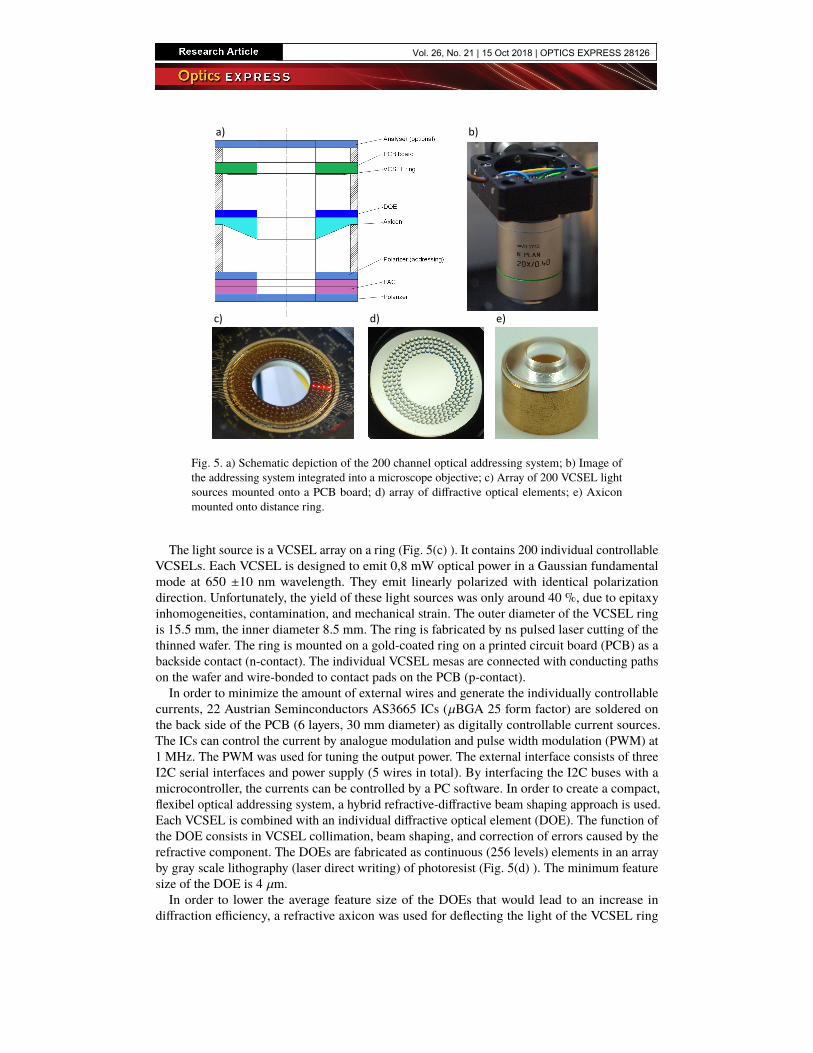
Fig. 5. a) Schematic depiction of the 200 channel optical addressing system; b) Image ofthe addressing system integrated into a microscope objective; c) Array of 200 VCSEL lightsources mounted onto a PCB board; d) array of diffractive optical elements; e) Axiconmounted onto distance ring.
The light source is a VCSEL array on a ring (Fig. 5(c) ). It contains 200 individual controllableVCSELs. Each VCSEL is designed to emit 0,8 mW optical power in a Gaussian fundamentalmode at 650 ±10 nm wavelength. They emit linearly polarized with identical polarizationdirection. Unfortunately, the yield of these light sources was only around 40 %, due to epitaxyinhomogeneities, contamination, and mechanical strain. The outer diameter of the VCSEL ringis 15.5 mm, the inner diameter 8.5 mm. The ring is fabricated by ns pulsed laser cutting of thethinned wafer. The ring is mounted on a gold-coated ring on a printed circuit board (PCB) as abackside contact (n-contact). The individual VCSEL mesas are connected with conducting pathson the wafer and wire-bonded to contact pads on the PCB (p-contact).In order to minimize the amount of external wires and generate the individually controllable
currents, 22 Austrian Seminconductors AS3665 ICs (µBGA 25 form factor) are soldered onthe back side of the PCB (6 layers, 30 mm diameter) as digitally controllable current sources.The ICs can control the current by analogue modulation and pulse width modulation (PWM) at1 MHz. The PWM was used for tuning the output power. The external interface consists of threeI2C serial interfaces and power supply (5 wires in total). By interfacing the I2C buses with amicrocontroller, the currents can be controlled by a PC software. In order to create a compact,flexibel optical addressing system, a hybrid refractive-diffractive beam shaping approach is used.Each VCSEL is combined with an individual diffractive optical element (DOE). The function ofthe DOE consists in VCSEL collimation, beam shaping, and correction of errors caused by therefractive component. The DOEs are fabricated as continuous (256 levels) elements in an arrayby gray scale lithography (laser direct writing) of photoresist (Fig. 5(d) ). The minimum featuresize of the DOE is 4 µm.In order to lower the average feature size of the DOEs that would lead to an increase in
diffraction efficiency, a refractive axicon was used for deflecting the light of the VCSEL ring
Vol. 26, No. 21 | 15 Oct 2018 | OPTICS EXPRESS 28126
into the centre. The axicon is fabricated by diamond turning low stress PMMA (Fig. 5(e) ). Inorder to filter out depolarized light due to residual birefringence of the PMMA or stray light, athin film polarizer (nanoparticle polarizer from Codixx AG) is mounted in front of the PAC. Theoverall light transmission efficiency of the addressing system is 64 % (including Fresnel effects).The outer diameter of the beam shaping optics is 19.5 mm and fits into the mechanics of a
Leica N Plan 20x/0,4 microscope objective lens. The length of the complete system including thePAC is 23 mm. The PCB board has an outer diameter of 30 mm. The clear transmission apertureof the system is 8,5 mm.
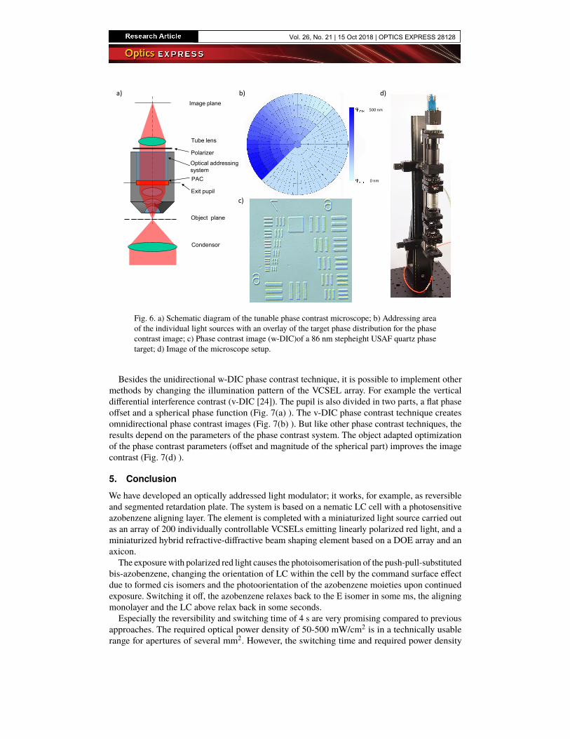
By exchanging the DOE plate, different addressing patterns can be achieved. In this approach,we divided an 8 mm active diameter into 200 individual controllable segments of equal area size(Fig. 6(b) ).
The overall system including the PAC is called ’active micro-optics for polarization control’(AMiPola) and is mounted in a microscope objective (Fig. 5(b) ).
4. Application: Tunable phase contrast
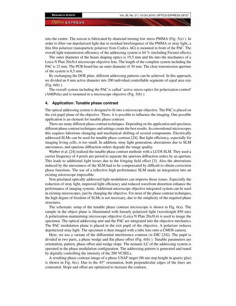
The optical addressing system is designed to fit into a microscope objective. The PAC is placed onthe exit pupil plane of the objective. There, it is possible to influence the imaging. One possibleapplication is an element for tunable phase contrast.
There are many different phase contrast techniques. Depending on the application and specimen,different phase contrast techniques and settings create the best results. In conventional microscopesthis requires laborious changing and mechanical shifting of several components. Electricallyaddressed SLMs can be used for tunable phase contrast [24]. But light efficiency, especially forimaging living cells, is too small. In addition, stray light generation, aberrations due to SLMunevenness, and spurious diffraction orders degrade the image quality.
Warber et al. [24] realized the tunable phase contrast methods with a LCOS SLM. They used acarrier frequency of 4 pixels per period to separate the spurious diffraction orders by an aperture.This leads to additional light losses due to the fringing field effect [3]. Also the aberrationsinduced by the unevenness of the SLM had to be compensated by difficult to obtain correctionphase functions. The use of a reflective high performance SLM made an integration into anexisting microscope impossible.Non-pixelated optically addressed light modulators can improve those issues. Especially the
reduction of stray light, improved light efficiency and reduced wavefront distortion enhance theperformance of imaging systems. Additional microscope objective integrated system can be usedin existing microscopes, just by changing the objective. For most of the phase contrast techniques,the high degree of freedom of SLMs is not necessary, due to the simplicity of the required phasestructures.The schematic setup of the tunable phase contrast microscope is shown in Fig. 6(a). The
sample in the object plane is illuminated with linearly polarized light (wavelength 850 nm).A polarization-maintaining microscope objective (Leica N Plan 20x/0,4) is used to image thespecimen. The optical addressing unit and the PAC are integrated into the objective mechanics.The PAC modulation plane is placed in the exit pupil of the objective. A polarizer reducesdepolarized stray light. The specimen is then imaged with a tube lens onto a CMOS camera.Here, we use a variant of the differential interference contrast (w-DIC [24]). The pupil is
divided in two parts, a phase wedge and flat phase offset (Fig. 6(b) ). Tunable parameters areorientation, pattern, phase offset and wedge slope. The nematic LC of the addressing system isoperated in the phase modulation configuration. The addressing pattern is generated and tunedby digitally controlling the intensity of the 200 VCSELs.A resulting phase contrast image of a phase USAF target (86 nm step height in quartz glas)
is shown in Fig. 6(c). Due to the 45o orientation, both perpendicular edges of the lines arecontrasted. Slope and offset are optimized to increase the contrast.
Vol. 26, No. 21 | 15 Oct 2018 | OPTICS EXPRESS 28127
a) b) d)
c)
Object plane
Exit pupil
Image plane
PAC
Tube lens
Polarizer
Condensor
Optical addressingsystem
500 nm
0 nm
Fig. 6. a) Schematic diagram of the tunable phase contrast microscope; b) Addressing areaof the individual light sources with an overlay of the target phase distribution for the phasecontrast image; c) Phase contrast image (w-DIC)of a 86 nm stepheight USAF quartz phasetarget; d) Image of the microscope setup.
Besides the unidirectional w-DIC phase contrast technique, it is possible to implement othermethods by changing the illumination pattern of the VCSEL array. For example the verticaldifferential interference contrast (v-DIC [24]). The pupil is also divided in two parts, a flat phaseoffset and a spherical phase function (Fig. 7(a) ). The v-DIC phase contrast technique createsomnidirectional phase contrast images (Fig. 7(b) ). But like other phase contrast techniques, theresults depend on the parameters of the phase contrast system. The object adapted optimizationof the phase contrast parameters (offset and magnitude of the spherical part) improves the imagecontrast (Fig. 7(d) ).
5. Conclusion
We have developed an optically addressed light modulator; it works, for example, as reversibleand segmented retardation plate. The system is based on a nematic LC cell with a photosensitiveazobenzene aligning layer. The element is completed with a miniaturized light source carried outas an array of 200 individually controllable VCSELs emitting linearly polarized red light, and aminiaturized hybrid refractive-diffractive beam shaping element based on a DOE array and anaxicon.
The exposure with polarized red light causes the photoisomerisation of the push-pull-substitutedbis-azobenzene, changing the orientation of LC within the cell by the command surface effectdue to formed cis isomers and the photoorientation of the azobenzene moieties upon continuedexposure. Switching it off, the azobenzene relaxes back to the E isomer in some ms, the aligningmonolayer and the LC above relax back in some seconds.
Especially the reversibility and switching time of 4 s are very promising compared to previousapproaches. The required optical power density of 50-500 mW/cm2 is in a technically usablerange for apertures of several mm2. However, the switching time and required power density
Vol. 26, No. 21 | 15 Oct 2018 | OPTICS EXPRESS 28128

a) b)
c) d)
500 nm
500 nm
0 nm
0 nm
Fig. 7. a) Un-optimized addressing pattern of the individual light sources with an overlayof the target phase distribution for the phase contrast image (b); b) Un-optimized v-DICphase contrast image of rabbit taste bud cells c) Optimized addressing pattern for the phasecontrast image (d); d) Optimized v-DIC phase contrast image of rabbit taste bud cells.
might be further decreased by optimizing the molecule structure, LC material, and self-assembledmonolayer parameters. Also, spatial resolution and behaviour in a wider addressing wavelengthspectrum might be characterized in detail.The 200 channels offer the possibility to create high density optical addressing systems.
The transmission efficiency can be further increased by optimising the DOE fabrication andapplication of anti-reflection coatings. Particularly the yield of the VCSEL light sources could beimproved to create entirely usable systems. In addition, more application-specific and complexaddressing patterns will extend the degree of freedom of an optical addressing system.Compared to conventional electrically addressed SLMs the proposed optically addressed
system has several advantages. The light efficiency of the modulator based on a PAC is higher,due to the absence of stray light and spurious diffraction orders generated by conducting wiresand electrodes. Wavefront distortion by the elements of the modulator is smaller because of thesimple low temperature coating fabrication process. The shape of the modulator can be adaptedeasily to different sizes and forms. It can be used with high efficiency as a transmission element,this makes integration in existing optical systems easy. Modulator area and spatial resolution canbe tuned by the optical addressing system.Electrically addressed SLMs have several millions of individual addressable pixels, higher
switching speed and do not require an optical addressing system. They are favored devices forfast switching of complex patterns. Optical addressed systems based on PACs can generate highermodulation quality and introduce less aberrations. But due to the optical addressing system theyare preferred applicable to use cases with medium pattern variation complexity.
Vol. 26, No. 21 | 15 Oct 2018 | OPTICS EXPRESS 28129

Especially imaging applications benefit from those advantages. Besides tunable phase contrast,dynamic aberration compensation, polarization imaging or scatterometry are possible uses. Inillumination systems, the low stray light level is beneficial to dynamic polarized illuminationpatterns e.g. in semiconductor inspection systems. This setup can be also used for tunable beamshaping e.g. for optical tweezers or polarized laser scanning microscopes.The application of an integrated microscope increases possible uses. The implementation
of other phase contrast techniques, like Zernike phase contrast or the tuning of polarizationproperties in imaging or illumination of technical surfaces, might be other applications. In thefuture, the system enables the creation of all-optical systems. Properties of light like polarisationor phase can be altered directly with light, without using electrical components.
Funding
Deutsche Forschungsgemeinschaft (DFG) (OS111/35-1, STU164/29-1 and MI500/22-1) withinthe priority program "Active Micro-optics" (SPP 1337).
Vol. 26, No. 21 | 15 Oct 2018 | OPTICS EXPRESS 28130