optical spectroscopy of individual single-walled carbon ... · carbon nanotubes are either metallic...
TRANSCRIPT

Optical Spectroscopy of Individual
Single-Walled Carbon Nanotubes
in an Electric Gate Structure:
Tuning the Photoluminescence
with Electric Fields
Dissertation der Fakultät für Physik
der Ludwig-Maximilians-Universität München
vorgelegt von
Jan Tibor Glückert
München, Januar 2014

Erstgutachter: Prof. Alexander Högele
Zweitgutacher: Prof. Achim Hartschuh
Datum der Verteidigung: 27. Januar 2014

Figure 0.1.: A metal-oxide-semiconductor capacitor for spectroscopy of individual carbonnanotubes
III


Zusammenfassung
Halbleitende, einwandige Kohlenstonanoröhren (CNTs) weisen abhängig von ihrerChiralität eine Bandstruktur aufgrund ihres eindimensionalen Gitters auf. DurchRekombination von Exzitonen emittieren CNTs Photolumineszenzlicht, das je nachRöhrendurchmesser im nahen bis mittleren Infrarotbereich liegt. Vor deren Rekom-bination diundieren Exzitonen entlang der Röhre. Dadurch sondieren sie nach Git-terplätzen, welche ein Umklappen ihres Spins verursachen, Exzitonen nicht-strahlendrekombinieren, oder, bei genügend tiefen Temperaturen, Exzitonen in null-dimensi-onalen Quantenpunkten lokalisieren. Daher zielt die (zeitaufgelöste) Spektroskopieeinzelner CNTs nicht nur auf die intrinsische Dynamik von Exzitonen, wie derenDiusion und Lebenszeit, sondern eben auch auf Störungen der näheren Umgebungoder im Gitter selbst. So können extrinsische und intrinsische Störungen zur Unter-drückung von Photolumineszenzsignalen, zum Aufhellen dunkler Exzitonzuständeoder zur Erzeugung von geladenen Exzitonzuständen führen.Im Rahmen dieser Arbeit wurden zur Untersuchung von Exzitonen in CNTs zwei
Ansätze verfolgt: Zum einen wurde die CNT Umgebung durch ein statisches elek-trisches Feld variiert, zum anderen wurden CNTs von ihrer Umgebung isoliert. ZurSpektroskopie einzelner CNTs fanden verschiedene Techniken der optischen Spek-troskopie Anwendung, wie zum Beispiel Anregungsspektroskopie, (zeitlich aufgelöste)Photolumineszenz-Spektroskopie und Photonen-Korrelationsspektroskopie.Diese Arbeit zeigt die zentrale Rolle von Exzitonenlokalistaion in CNTs bei tiefen
Temperaturen auf. So zeigten bei tiefen Temperaturen die Photolumineszenz vonCNTs auf dielektrischen Substraten asymmetrische Linenformen und bei steigen-den Temperaturen systematische Energieverschiebungen zum Blauen. Zudem wardie Photolumineszenz spektraler Diusion unterworfen, die - wie auch schon vonHalbleiter-Quantenpunkten bekannt - durch einzelne Ladungsuktuatoren im nahendielektrischen Medium hervorgerufen wurde. Zusätzliche Hinweise auf die Lokalisa-tion von Exzitonen lieferte die nicht-klassische Einzel-Photonen-Emission von kaltenCNTs.Das Hauptaugenmerk lag jedoch auf der Untersuchung einzelner CNTs in statis-
chen elektrischen Feldern. Mittels einer Metall-Oxid-Halbleiter Struktur wurde zu-nächst die transversale Polarisation von Exzitonen vermessen. Abhängig vom an-gelegten senkrechten Feld zeigte die Energie der Photolumineszenz eine quadratischeDispersion. Eine Unterklasse von CNTs zeichnet sich jedoch durch mehrere Linienim Emissionsspektrum aus. Aufgrund von der charakteristischen Abstände dieserLinien wurden sie eindeutig dunklen Exzitonzuständen, genauer Triplett- und "k-momentum"-Zuständen, zugeordnet. Ein weitere charakteristischer Energieabstandergab sich in Spektren, die das Aufhellen einer zusätzlichen Linie in Abhängigkeitvom elektrischen Feld zeigten. Diese Linien konnten eindeutig geladenen Exzito-nen (Trionen) zugeordnet werden, und entstammen der Dotierung einzelner CNTsmittels Ladungen aus Oxidzuständen des nahen Dielektrikums. Solche Oxidladun-gen spielten vermutlich auch bei der Veränderung der Anregungsspektren einzelnerCNTs eine wichtige Rolle. Da diese Veränderung abhängig vom angelegten Feld war,liegt es nahe, dass sie durch eine Variation des Lokalisationspotentials für Exzitonenverursacht wurde.Abschlieÿend, dem Einuss externer Variationen aus dem dielektrischen Medium
stehen die einzigartigen optischen Eigenschaften von freihängenden CNTs entgegen.Diese freihängenden Röhren wiesen isoliert lokalisierte Exzitonen und in Konsequenz
V
sehr schmale Linienbreiten, nahezu intrinsische Lebenszeiten und eine merklich er-höhte Fluoreszenzausbeute auf. Auÿerdem, zeigten sie selbst auf kürzesten Zeitskalenweder spektrale Diusion noch Periodizitäten der Intensität.
VI
Abstract
Semiconducting single-walled carbon nanotubes (CNTs) exhibit a chirality dependedband structure of a one-dimensional lattice. Due to the radiative recombination ofexcitons CNTs emit photoluminescence in the near and mid infrared ranges depend-ing on the tube diameter. Excitons are subject to diusion along the tube beforeradiative recombination. Thereby they probe sites that give rise to spin-ips ornon-radiative decay, or, at cryogenic temperatures, they localize in zero-dimensionalquantum dots at the minima of the local energy potential landscape. Thus, the opti-cal spectroscopy of individual CNTs probes not only the intrinsic exciton dynamics,like diusion and intrinsic life-time, but also disorder of the CNT lattice and itsenvironment. Intrinsic and extrinsic inhomogeneities and impurities may give riseto photoluminescence quenching, brightening of dark exciton states or generation ofcharged exciton complexes.In the framework of this thesis the physics of excitons in CNTs was investigated
in two ways: On the one hand their environment was varied with an static electriceld, on the other hand the CNTs were isolated from their environment. A compre-hensive set of optical spectroscopy techniques was used to study individual CNTsat low temperatures. This included photoluminescence excitation, (time-resolved)photoluminescence, and photon correlation spectroscopy.This work identied exciton localization as predominant feature of individual CNTs
at cryogenic temperatures. CNTs on substrate exhibited asymmetric line shapes atlow temperature and temperature dependent shifts on the PL energy. Moreover forconstant temperature, PL energies were subject to spectral diusion, which arose- in analogy to compound semiconductor quantum dots - from interaction with afew close charge uctuators in the dielectric environment. In addition, evidence forexciton localization was provided by the non-classical photon emission statistics ofcryogenic CNTs.The main focus of this thesis was the study of individual CNTs in a static electric
eld. A metal-oxide-semiconductor device was used to probe for the transverse po-larizability of excitons. In consequence, the PL energy of CNTs exhibited red-shiftsas a quadratic function of the perpendicular electric eld. However, a subclass ofCNTs was characterized by satellite peaks in the emission prole. By their energysplitting they were assigned to PL emission from dark exciton states, e.g. triplet andk-momentum excitons, and resulted presumably from impurity induced symmetrybreaking. As a function of the electric eld, CNTs with a broken symmetry featuredlinear shifts of the PL energy of bright and triplet excitons. A third energy scalein the exciton ne structure was manifested by CNTs that exhibited the emergenceof a satellite peak as a function of the electric eld. These satellites were assignedto the PL of trions generated by doping of individual CNTs with charges from closeoxide states. Presumably such close charge states played also an important role inthe variation of the excitation spectra of individual CNTs, which was observed as afunction of the applied electric eld. This variation could be mediated by switchingof charge states, which varied the localization potential of excitons.Finally, the extrinsic eects of the surrounding dielectric medium were contrasted
by the remarkable optical properties of as-grown suspended CNTs. Freely suspendedCNTs featured isolated localized excitons with narrow linewidths, intrinsic excitonlifetime and a signicantly increased quantum yield. Moreover, they lack signaturesof spectral diusion or intermittency even on the shortest timescales.
VII


Contents
1. Introduction 3
2. Theoretical considerations 7
2.1. Geometric properties . . . . . . . . . . . . . . . . . . . . . . . . . . . 7
2.1.1. From graphene to carbon nanotubes . . . . . . . . . . . . . . 7
2.1.2. Symmetry considerations . . . . . . . . . . . . . . . . . . . . 11
2.2. Electronic states in carbon nanotubes . . . . . . . . . . . . . . . . . 13
2.2.1. Electronic properties . . . . . . . . . . . . . . . . . . . . . . . 13
2.2.2. Density of states . . . . . . . . . . . . . . . . . . . . . . . . . 15
2.2.3. First approach to optical selection rules . . . . . . . . . . . . 16
2.3. Excitons . . . . . . . . . . . . . . . . . . . . . . . . . . . . . . . . . . 18
2.3.1. Screening of Coulomb interaction . . . . . . . . . . . . . . . . 18
2.3.2. Binding energy . . . . . . . . . . . . . . . . . . . . . . . . . . 18
2.3.3. Symmetry of exciton states . . . . . . . . . . . . . . . . . . . 21
2.3.4. Selection rules for optical transitions . . . . . . . . . . . . . . 23
2.3.5. Photoluminescence . . . . . . . . . . . . . . . . . . . . . . . . 24
2.3.6. Exciton ne structure . . . . . . . . . . . . . . . . . . . . . . 25
3. Photoluminescence of individual carbon nanotubes 29
3.1. Laser setup and confocal microscope . . . . . . . . . . . . . . . . . . 30
3.1.1. Confocal microscope . . . . . . . . . . . . . . . . . . . . . . . 30
3.1.2. Laser power stabilization . . . . . . . . . . . . . . . . . . . . . 32
3.2. Sample preparation and characteristics . . . . . . . . . . . . . . . . . 35
3.2.1. Metallic grid . . . . . . . . . . . . . . . . . . . . . . . . . . . 36
3.2.2. CoMoCat material . . . . . . . . . . . . . . . . . . . . . . . . 36
3.3. Spatially resolving imaging techniques . . . . . . . . . . . . . . . . . 36
3.4. Signatures of individual CoMoCat CNTs . . . . . . . . . . . . . . . . 39
3.5. Exciton localization at low temperatures . . . . . . . . . . . . . . . . 41
IX

Contents
4. Tuning the photoluminescence with electric elds 47
4.1. Electric eld structure . . . . . . . . . . . . . . . . . . . . . . . . . . 48
4.1.1. Growth and characterization of thin lms . . . . . . . . . . . 48
4.1.2. Ohmic contacts . . . . . . . . . . . . . . . . . . . . . . . . . . 50
4.2. Capacitance-voltage characterization . . . . . . . . . . . . . . . . . . 52
4.2.1. Ideal MOS capacitor . . . . . . . . . . . . . . . . . . . . . . . 52
4.2.2. Measuring the capacitance . . . . . . . . . . . . . . . . . . . . 56
4.2.3. Total charge state density Qtot . . . . . . . . . . . . . . . . . 57
4.3. Jitter analysis . . . . . . . . . . . . . . . . . . . . . . . . . . . . . . . 59
4.3.1. Energy jumps . . . . . . . . . . . . . . . . . . . . . . . . . . . 60
4.3.2. Intermittency and blinking . . . . . . . . . . . . . . . . . . . 62
4.4. Classication of CNTs . . . . . . . . . . . . . . . . . . . . . . . . . . 64
4.4.1. Multiple peak emission spectra . . . . . . . . . . . . . . . . . 64
4.4.2. Emission spectra of type A and type B CNTs . . . . . . . . . 67
4.5. Electric eld sweeps . . . . . . . . . . . . . . . . . . . . . . . . . . . 67
4.5.1. Transverse polarizability of excitons . . . . . . . . . . . . . . 68
4.5.2. Permanent dipole moments . . . . . . . . . . . . . . . . . . . 70
4.6. Emission from trion states . . . . . . . . . . . . . . . . . . . . . . . . 74
4.7. Tuning the localization potentials of excitons . . . . . . . . . . . . . 78
4.7.1. Photoluminescence excitation spectroscopy . . . . . . . . . . 78
4.7.2. Tuning excitation resonances with the gate voltage . . . . . . 81
5. Photon emission statistics 85
5.1. Theoretical introduction . . . . . . . . . . . . . . . . . . . . . . . . . 86
5.1.1. Second-order correlation function . . . . . . . . . . . . . . . . 86
5.1.2. Blinking and intermittency . . . . . . . . . . . . . . . . . . . 88
5.1.3. Single photon emitters . . . . . . . . . . . . . . . . . . . . . . 90
5.1.4. Photon emission statistics of blinking carbon nanotubes . . . 92
5.2. Hanbury-Brown and Twiss interferometer . . . . . . . . . . . . . . . 94
5.2.1. Basic considerations . . . . . . . . . . . . . . . . . . . . . . . 94
5.2.2. Hanbury-Brown and Twiss interferometer setup . . . . . . . . 97
5.2.3. Reducing the cross talk . . . . . . . . . . . . . . . . . . . . . 99
5.3. Freely suspended carbon nanotubes . . . . . . . . . . . . . . . . . . . 101
5.3.1. As-grown suspended CNTs . . . . . . . . . . . . . . . . . . . 102
5.3.2. Methods . . . . . . . . . . . . . . . . . . . . . . . . . . . . . . 104
5.3.3. Spectral properties . . . . . . . . . . . . . . . . . . . . . . . . 104
5.3.4. Photoluminescence lifetime . . . . . . . . . . . . . . . . . . . 106
X

Contents
5.3.5. Photon emission statistics . . . . . . . . . . . . . . . . . . . . 107
Summary and perspectives 113
Appendix 119
A. Notation and physical constants 119
A.1. Physical and material constants . . . . . . . . . . . . . . . . . . . . . 119
A.2. Symbols and abbreviations . . . . . . . . . . . . . . . . . . . . . . . . 120
B. Exchange and trion binding energy 123
C. Protocol for fabrication of layers with individualized carbon nanotubes 125
D. Model for excitation of localized excitons 127
Bibliography 135
List of Publications 157
Danksagung 159
1


1. Introduction
Since carbon nanotubes were observed by Sumio Iijima in 19911 [2], investigations
and applications of single- and multi-walled nanotubes have triggered great progress
in physics [3], chemistry [4], mechanical [5] and electrical engineering [6] as well as bi-
ology [7], pharmacy [8] and medicine [9]. Today, carbon nanotubes have become one
of the most intensively studied materials in the eld of nanotechnology [10]. Formed
from a single mono-layer of a hexagonal carbon lattice (graphene) into seamless
tubes, carbon nanotubes consist of an almost perfectly-dened lattice down to the
atomic scale. Held together by strong covalent carbon-carbon bonds, they exhibit ex-
traordinary mechanical properties [11]. In fact, carbon nanotubes feature the highest
reported values of tensile strength [12] and stiness [13] and thus are now employed
routinely for reinforcement of metal composites [14], polymer matrices and ceram-
ics [15]. In 2013 the world-wide production capacity for nanotubes reached a level
of 5000 tons per year and is prospected to double within the next 30 months [16].
Carbon nanotubes are either metallic or semiconducting2, which depends on the
orientation of the hexagonal lattice along the tube [17, 18]. The band-gap of semi-
conducting single-walled carbon nanotubes (CNTs) varies inversely proportional to
the diameter with values ranging from a few meV up to 2 eV [19]. Further, CNTs
feature an enormous aspect ratio: The diameter of the thinnest CNTs were ob-
served with only 3 Å [20] whereas the length exceeded the limits of the nano-scale
with nearly foot-long CNTs reported recently [21]. Thus, CNTs are considered a
paradigm system for the study of one-dimensional physics [22], which includes exotic
eects of spin-charge separation or Wigner crystals characteristic for one-dimensional
Luttinger liquids [23].
CNTs exhibit absorption [24] and emission [25] in the near-infrared and both ab-
sorption and photoluminescence (PL) spectroscopy were extensively used to deter-
mine the optoelectronic properties of individual CNTs [2427]. Because of their
1In 1952 V. Radushkevich and V. M. Lukyanovich [1] reported on their observation of carbontubes with a diameter of 50 nm. However, their work remained unnoticed for long time untilIijima triggered further investigation of carbon nanotubes.
2In the following we consider only semiconducting single-walled carbon nanotubes, which will beabbreviated as CNTs.
3

1. Introduction
excellent optical properties CNTs are proposed for a variety of application in op-
toelectronics including solar cells [28] as well as ecient photo detectors and emit-
ters [29] that can be tailored specically to a wavelength by the choice of the tube
diameter.
Due to their low-dimensionality CNTs feature generally a reduced screening of
the Coulomb interaction [3033]. The screening aects the entire energy hierarchy
giving rise to enormous exciton binding energies, as large as 800-1000 meV for small
diameter CNTs in vacuum [3436]. Thus, the optics of CNTs are dominated by
excitons even at room temperature [27,36,37]. There are four exciton ground states,
of which only one is optically bright [38]. The lowest energetic exciton state is dipole
forbidden by symmetry and termed as the dark exciton. In nite magnetic elds
along the CNT axis however, emission from the dark exciton state was observed [39
41]. Further, there is the doubly degenerate k-momentum exciton state. Although
radiative recombination from this state is momentum forbidden, it can be brightened
given sucient exciton-phonon coupling [42, 43]. Single impurities and ad-atoms
were identied to increase spin-orbit coupling and to brighten dark triplet exciton
states [4446]. Furthermore charged exciton states (trions) were observed [4751].
This thesis considers the spectroscopy of individual CNTs, mainly at cryogenic
temperature. As theoretical introduction, chapter 2 focuses on the dierent exciton
states in CNTs [52]. Beginning with their geometry, we discuss direct and indirect
lattices with special regard to symmetry [53]. These geometric considerations are
further used to identify the electronic band structure of CNTs and provide numbers
for the diameter-dependent band-gap [54]. Based on symmetry considerations, the
four states of the exciton singlet manifold and their optical activity are discussed [38].
We include also exciton triplet states [55] and trions [56, 57] and present for all
small-diameter CNTs an overview on the exciton ne structure and the respective
energy-splitting to the bright exciton [34].
Chapter 3 presents the lay-out and specications of the experimental setup, namely
a confocal microscope operated at cryogenic temperature and a tunable laser source
with an actively stabilized power output - a basic requirement for photoluminescence
excitation spectroscopy. Further, methods for preparation and ecient characteri-
zation of individualized CNTs are addressed. This includes complementary imaging
techniques, viz. atomic force microscopy, scanning electron microscopy and micro-
luminescence spectroscopy. We present PL spectra from individual CNTs consisting
of a single emission line [27, 37, 58] that is assigned to the bright exciton emission.
By variation of the temperature from cryogenic (T=4.2 K) to room temperature, we
4

identify systematic variation of the PL emission of individual CNTs. Asymmetric
line shape [59,60] and temperature induced blue shifts on the PL energy [6163] are
both indicative for the localization of excitons at cryogenic temperature. Exciton
localization may arise from singular impurities [62]. PL signals are highly sensitive
to variations in the CNT structure as well as the immediate surrounding. Except for
two-dimensional atomic layers such as graphene, CNTs exhibit the highest possible
surface-to-volume ratio. Since the shell is but a single monolayer, all atoms reside
on the tube surface. In pristine CNTs excitons are expected to exhibit an intrinsic
lifetime of ∼ 10 ns [64,65]. Thus, long exciton diusion lengths have been observed,
which, at room temperature, exceed 200 nm [66] and range up to 610 nm [67] - far
beyond the exciton Bohr radius [68]. During diusion an exciton passes more than
ten thousands lattice sites thereby sampling extrinsic and intrinsic inhomogeneities,
which give rise to non-radiative recombination channels [69] and exciton dephas-
ing [70]. Hence, the PL intensity of CNTs is sensitive to single disordered sites, be
they due to the substrate [71], chemically adsorped atoms or molecules at the tube
surface [72, 73] or mono-vacancy lattice defects [74]. This quantum-dot-like behav-
ior is apparent in the conductance of single CNTs that is dominated by Coulomb
blockade [75]. Further, PL emission from highly localized bright spots along a CNT
was also observed in near-eld microscopy [58,61]. And nally, also the non-classical
photon emission statistics of individual CNTs was associated with the localization of
excitons [76,77].
In addition to one peak spectra, chapter 4 considers also CNTs that feature satel-
lite peaks in their PL spectra. These additional spectral features are assigned to
symmetry breaking, which admixes bright and dark exciton states and brightens
triplet [78, 79] and k-momentum excitons [80]. A third energy scale is manifested
by CNTs that exhibit the emergence of a satellite peak as a function of an exter-
nally applied electric eld. This energy scale agrees with theoretical [55, 81] and
experimental [47, 49, 50] reports for the trion emission energy. Exciton charging is
presumably generated by doping of CNTs from the surrounding dielectric medium.
Furthermore, the transverse polarization of excitons [82] was studied as a function
of an electric eld perpendicular to the CNT axis. For CNTs with a preserved sym-
metry the PL showed a quadratic energy dispersion. However, CNTs with a broken
symmetry showed linear shifts on the PL energy. Finally, this chapter considers the
PL intensity from the bright exciton as a function of the laser detuning. In addition
to the higher energetic electronic E22 manifold, the importance of phonon-sidebands
is reported for the ecient generation of excitons at cryogenic temperature [8387].
5

1. Introduction
We use photoluminescence excitation spectroscopy [88] to reveal the excitation spec-
tra of individual CNTs. Within our studies the excitation spectra are varied by
means of the externally applied electric eld.
Chapter 5 begins with a brief theoretical discussion of the second-order correla-
tion function and further presents the setup and specications of a Hanbury-Brown
and Twiss interferometer employed for time-resolving spectroscopy. In addition to
spectral resolving PL spectroscopy, photon counting spectroscopy is applied in com-
parative studies of CNTs supported by a dielectric substrate and as-grown suspended
CNTs. We record PL lifetime traces and photon emission statistics for both species.
All investigated CNTs exhibit non-classical photon emission [76, 77]. However, sig-
natures of photon-bunching [89], which arise from fast intermittency [77], are only
present for CNTs interacting with their dielectric surrounding. Due to isolation from
any dielectrics as-grown suspended CNTs feature ultra-narrow PL linewidth, nearly
intrinsic exciton lifetime, and a signicantly increased quantum yield.
The thesis concludes with a nal summary giving an overview on our ndings. As
an outlook it proposes for further experimental investigation, which could benet
from the remarkable optical properties of as-grown suspended CNTs presented here.
6

2. Theoretical considerations
The following theoretical introduction gives a brief overview of the physical properties
of pristine single-walled carbon nanotubes1. Starting with a mono-layer of graphene,
carbon nanotubes are discussed with regard to their geometric characteristics that
determine all other physical properties. For a deeper understanding it is fruitful to
consider the symmetry of pristine carbon nanotubes, which allows to predict the
impact of symmetry breaking due to external perturbations or single lattice defects.
A main focus lies on the optical properties that can be understood in terms of creation
of bound electron-hole pairs (excitons) and their decay.
2.1. Geometric properties
2.1.1. From graphene to carbon nanotubes
Direct lattice
Graphene is formed as mono-atomic (two-dimensional) hexagonal lattice by sp2-
hybridized carbon atoms each bonding with three neighboring atoms [90]. A section
of this honeycomb lattice is illustrated in Fig. 2.1(a). The unit cell consists of two
atoms, which dene two intersecting sublattices. The lattice vectors ~a1 and ~a2 are
commonly dened by
~a1 =
( 32√3
2
)· acc and ~a2 =
( 32
−√
32
)· acc (2.1)
where acc = 0.142 nm gives the bond length between two carbon atoms.
For illustrative creation of a carbon nanotube a graphene ribbon rolls up to form
a seedless cylinder. The resulting tubes dier in their diameter dt and in the orienta-
tion of the honeycomb lattice with respect to the cylinder axis. Both, the orientation
and the diameter, are determined by the chiral vector ~Ch, which connects two crys-
tallographic equivalent lattice sites. These sites come to lie on each other when a
1We emphasize that thesis considers only single-walled carbon nanotubes.
7

2. Theoretical considerations
Figure 2.1.: Construction of a carbon nanotube from a layer of graphene: Thegrey honeycomb lattice and the basis vectors ~a1 and ~a2 are depicted. (a) Theconstruction of a tube with the chiral index (4,2) results in the translation vector~T and the chiral vector ~Ch, that includes the chiral angle θ with ~a1. (b) θ denesthree classes of carbon nanotubes: zig-zag (θ = 0), armchair (θ = 30) andchiral (0 < θ < 30). (Adapted from Ref. [91])
graphene ribbon is rolled up to a nanotube. ~Ch can be expressed as the sum of
integer multiples of ~a1 and ~a2
~Ch = n · ~a1 +m · ~a2 with n,m ε N . (2.2)
Hence, the integers n and m are sucient to describe explicitly the nanotube struc-
ture. Commonly, they are used in the form (n,m) termed as chiral index or chirality
of a carbon nanotube. Due to the symmetry of graphene, a tube with the chiral index
(x, y) is identical to a second with (y, x). Therefore, it is a common convention that
n ≥ m without loss of generality.
An innitely long carbon nanotube is invariant under translation of integer mul-
tiples of the unit translation vector ~T along the tube axis. Hence, ~T is always
perpendicular to ~Ch:
~Ch · ~T = 0 . (2.3)
To determine the unit translation vector - the shortest of all vectors perpendicular
to ~Ch - we express ~T in the basis of ~a1 and ~a2. Further, we use the condition that t1and t2 (of the shortest vector) do not have a common divisor other than 1:
~T = t1~a1 + t2~a2 =2m+ n
dR~a1 +
2n+m
dR~a2 . (2.4)
Here, dR is dened as the greatest common divisor of 2n+m and 2m+ n. Knowing
8

2.1. Geometric properties
~Ch and ~T , we can deduce the number of hexagons per unit cell N . The area of the
nanotube unit cell is given by |~Ch × ~T |, whereas the area of the graphene unit cell
by |~a1 × ~a2|. Thus, we can write
N =|~Ch × ~T ||~a1 × ~a2|
=2(n2 + nm+m2)
dR. (2.5)
As two carbon atoms form the basis of the graphene unit cell, the number of carbon
atoms per nanotube unit cell equals 2N .
The chiral angle θ is enclosed between ~Ch and ~a1. It is connected to the chiral
index (n,m) by2
θ = arctan
( √3m
2n+m
)(2.6)
and is limited to 0 ≤ θ ≤ 30 since n ≥ m. As some carbon nanotubes exhibit ad-
ditional symmetries it is helpful to distinguish between three major classes. Firstly,
zig-zag nanotubes are characterized by θ = 0 or the chiral index (n, 0), secondly,
armchair nanotubes by θ = 30 or (n, n). We will show below that both have addi-
tional symmetry planes [92] and are achiral. Those CNTs without these symmetry
planes form the third class: chiral nanotubes with 0 < θ < 30 and accordingly
(n,m) with 0 < m < n. Fig. 2.1 depicts ~Ch, ~T , and θ for the construction of a chiral
carbon nanotube with chiral index (4,2). Furthermore, it shows the circumferen-
tial bonding path for armchair and zig-zag nanotubes, respectively. Their respective
path shape is eponym for these classes. Since the tube circumference is given by the
length of ~Ch, its diameter dt can be expressed in terms of the chiral index (n,m) by
dt =|~Ch|π
=
√3
πacc
√m2 +mn+ n2 . (2.7)
Reciprocal space
The reciprocal lattice of graphene is also hexagonal. It is spanned by the reciprocal
lattice vectors ~b1 and ~b2:
~b1 =
( 1√3
1
)· 2π
accand ~b2 =
( 1√3
−1
)· 2π
acc. (2.8)
2since cos θ =~Ch·~a1|~Ch||~a1|
9

2. Theoretical considerations
For a carbon nanotube it is useful to express all reciprocal vectors in the basis of
the following two vectors: ~K1 that accounts for the vector component along the
nanotube axis and ~K2 that accounts for the circumferential component only. That
is to say, ~K1 ( ~K2) is the reciprocal vector of ~T (~Ch). Therefore we can write
~Ch · ~K1 = 2π ~T · ~K2 = 2π
~T · ~K1 = 0 ~Ch · ~K2 = 0 .(2.9)
Using Eqs. (2.2), (2.4), and (2.8), the basis vectors of the reciprocal lattice can be
expressed as a function of the chiral index (n,m) by
~K1 =2n+m
NdR
~b1 −2m+ n
NdR
~b2
~K2 =m
N~b1 −
n
N~b2
(2.10)
where N is the number of hexagons per unit cell given in Eq. (2.5). When a graphene
ribbon is rolled up to a nanotube, any reciprocal wave vector ~k is composed of a
component along the tube axis k‖ and a circumferential component k⊥:
~k = k⊥ ~K1 + k‖ ~K2 . (2.11)
Within the rst Brillouin zone the parallel component k‖ can take any quasi-con-
tinuous value3 within [− π|~T |, π|~T |
], whereas the circumferential component k⊥ must
fulll an additional boundary condition. Due to destructive interference, all wave
functions that do not exhibit a phase shift of 2π (or multiples of 2π) around the
nanotube circumference vanish. Hence, k⊥ is constrained to the values
k⊥ = µ2π
|~Ch|(2.12)
where µ is an integer. Since a minimum of four 4 carbon atoms is needed to dene the
wavelength and every unit cell consists of 2N atoms, µ is limited to integer values4
within [−N2 ,
N2 [. In the following, the axial component k‖ is simply denoted by k
and the circumferential component by its quantum number µ.
Fig. 2.2 illustrates the allowed states (as cutting lines due to zone folding, see
Chap. 2.3) for a representative of each major group. Due to limited space, only the
3Here, an innitely long carbon nanotube is assumed.4In fact, the state −N
2is equivalent to N
2. Since this state should not be counted twice, either
−N2or N
2must be excluded.
10

2.1. Geometric properties
(c)(b)(a)
(4,4)(4,0)(4,2)
Γ
K
Kʼ
Γ
K
Kʼ
Γ
K
Kʼ
chiral zig-zag armchair
K1
K2
K1
K2K1
K2
Figure 2.2.: Reciprocal lattice of three dierent carbon nanotubes: First Brillouinzone of graphene and basis vectors ~K1 and ~K2 of a carbon nanotube (not toscale). The allowed states (cutting lines) are depicted as orange solid lines fora chiral (a), zig-zag (b) and armchair nanotube (c).
rst Brillouin zone of graphene is depicted. Of course, a substantial analysis would
require the entire rst Brillouin zone of the nanotube that consists of N hexagons.
Nevertheless, the illustration exemplies the main argument. While the allowed
states can intersect with the K or K ′ point in some chiral and zig-zag nanotubes,
this is always the case for armchair nanotubes. According considerations will play
an important role in the analysis of the electronic properties of carbon nanotubes
discussed in Chap. 2.2.
2.1.2. Symmetry considerations
The symmetry of a system determines many of its physical properties. For example
in an atom (molecule), the symmetry of the atomic (molecular) orbitals denes
the allowed optical transitions. Likewise, the optical activity of (organic) molecules
requires the lack of any axis of improper rotation [93]. Thus, examining a system with
regard to its symmetry facilitates calculations and may even enable for computation-
free predictions.
As shown in the previous paragraphs, carbon nanotubes exhibit an one-dimen-
sional lattice that is composed of a periodical sequence of unit cells along the trans-
lation vector ~T . The line groups contain all symmetries of such a system. These
were originally reported for all carbon nanotubes by Damnjanovic et al. [92]. It will
be briey summarized here since the notation will be used in the following analysis
of exciton states and selection-rules for optical transitions. An instructive review
11

2. Theoretical considerations
chiral zig-zag armchair
Figure 2.3.: Symmetry for chiral, zig-zag and armchair carbon nanotubes: All car-bon nanotubes are symmetric under rotations around U and U ′, which aregenerally denoted by C ′2 and C ′′2 , respectively. Achiral tubes (zig-zag and arm-chair) show symmetry mirror planes both horizontally (σh, σ
′h) and vertically
(σv, σ′v). Not depicted: All tubes are additionally symmetric under screw opera-
tions around the tube axis. Achiral tubes are further symmetric under rotationsaround the tube axis. (Adapted from Ref. [92])
on the symmetry-related properties of carbon nanotubes was published by Barros et
al. [53].
Damnjanovic et al. started out with a mono-layer of graphene and investigated
the preservation of its translation symmetry upon a carbon nanotube. Graphene is
symmetric under rotations of 180 around every lattice site or the midpoint of every
bonding. As illustrated in Fig. 2.3, these symmetries are preserved in all carbon nan-
otubes with the C ′2 (U) and C ′′2 (U ′) axis, respectively. Pure translation symmetries
of graphene turn into pure rotation or screw symmetries in carbon nanotubes. One
can make simple and illustrative predictions by considering a tube with chiral index
(n,m). If its chiral vector ~Ch can be divided into parts - that is the greatest common
divisor of n and m (here denoted as dn) is greater than 1 -, the tube is symmetric
under rotations by 2πdn
around its axis. The associated line group is termed as Csdn(with s = 0, 1...dn−1). Whereas chiral tubes never feature any mirror planes, achiral
tubes are additionally symmetric to mirror and glide5 planes, which are depicted in
Fig. 2.3.
Mathematically these symmetries are summarized in line groups. Every line group
L is a product of a point group P and an innite cyclic group T of generalized trans-
lations. For determination of the electronic properties it is sucient to consider the
point group only. Thus, translational symmetries T will be neglected in the follow-
5That is a combination of mirroring at a plane and a successive translation.
12

2.2. Electronic states in carbon nanotubes
π*
π
(b)(a)
electron hole
2pz
π*
π
2pz
Figure 2.4.: Electronic properties of graphene (a) Two pz orbitals form one bonding (π)and one anti-bonding (π∗) state. (b) Valence band (π) and conduction band(π∗) in the rst Brillouin zone. (Adapted from Ref. [90])
ing. The point group of a chiral nanotube is Ddn whereas achiral nanotubes exhibit
higher symmetry Dnh. We will further use the line group notation to represent
irreducibly an electronic state:
XΠk µ . (2.13)
Here, µ denotes the circumferential quantum number, Π the parity under C2 rotations
and k the wave vector along the tube. X can take the values A, B or E. The
rst two denote non-degenerate representations that are either even (A) or odd (B)
under vertical reection. E is the doubly degenerate representation. The complete
character tables for the Dn point group and thus for chiral nanotubes can be found
in Ref. [53].
2.2. Electronic states in carbon nanotubes
2.2.1. Electronic properties
By analogy with the geometric properties of carbon nanotubes, which we have de-
duced from those of graphene earlier in this chapter, we will deduce their electronic
properties on the basis of the graphene band structure. Instead of allowing all pos-
sible states, we just consider the periodic boundary conditions given by Eq. (2.12)
and the resulting constraints on possible wave vectors. This zone-folding gives an
illustrative and rough estimation of the electronic properties of a carbon nanotube -
even though it neglects all eects that arise from the tube curvature.
We begin with a single carbon atom that has four valence electrons distributed
13

2. Theoretical considerations
among the 2s, 2px, 2py and 2pz orbital [93]. The rst three of them are hybridized
to the in-plane sp2 states that form σ bonds each with one of the three neighboring
carbon atoms. Each pair of these three bonds include an angle of 120, which takes
shape in the previously discussed hexagonal lattice of graphene. Perpendicular to
this plane, the 2pz orbitals form weaker π bonds, which are illustrated in Fig. 2.4(a).
Due to this orthogonality, discussions of electrons in π and σ bonds can be separated.
Since the σ electrons are strongly bound, they can be neglected for the derivation of
the optical and electronic properties. Reich et al. reported a common approach in-
cluding a nearest neighbor tight-binding approximation with special regard to carbon
nanotubes [94]. The dispersion of the bonding π and the anti-bonding π∗ orbitals
forms the valence band (v) and the conduction band (c), respectively. The electronic
energy dispersion for graphene is approximated by6
Ev(c)(~k) =ε2p
+(−)γ0w(~k)
1 +(−)sw(~k)
(2.14)
with
w(~k) =
√√√√1 + 4 cos
(3kxacc
2
)cos
(√3kyacc
2
)+ 4 cos2
(√3kyacc
2
). (2.15)
Limiting the interaction only between nearest neighbors, the parameters are ε2p = 0,
s = 0.129 and the nearest-neighbor interaction γ0 = −3.033 eV [90]. Both dispersion
relations are illustrated in Fig. 2.4(b). The fully occupied valence band (π) and the
empty conduction band (π∗) are separated by an energy gap and intersect only at
the K and K ′ points located at the zone boundary. Since the density of states at
these points is zero, graphene is a semi-metal. At the K (K ′) points the bands form a
Dirac cone with a linear dispersion for electron and holes. As the second derivative of
the dispersion relation vanishes, electrons and holes feature an accordingly vanishing
eective mass close to the K and K ′ points. This is the main reason for the unique
electronic properties of graphene.
With regards to carbon nanotubes, we now use the aforementioned zone-folding
approach and limit the wave vectors to those that fulll the circumferential periodic
boundary condition. Using Eq. (2.12), Ev(c)(~k) is now limited in the circumferential
6ε2p, γ0 and s are used as tting parameters though they represent the orbital energy of the 2pzorbital, the transfer integral and the overlap integral with the nearest neighbor, respectively [90].
14

2.2. Electronic states in carbon nanotubes
direction to a few possible values µ. Therefore, we can write
Ev(c)(µ, k) = Ev(c)(k~K1
| ~K1|+ µ ~K2) with − π
|~T |< k <
π
|~T |and µ = −N
2, ...
N
2.
(2.16)
Using the explicit expressions for ~K1 and ~K2 given in Eq. (2.10), we obtain
w(~k)→ w(µ, k) =
[1 + 4 cos
(πµ(2n+m)
2(n2 + nm+m2)+mTk
2N
)×
cos
(3πµm
2(n2 + nm+m2)− (2n+m)Tk
2N
)+4 cos2
(πµ(2n+m)
2(n2 + nm+m2)+mTk
2N
)] 12
.
(2.17)
Since the conduction and valence band intersect only at the K (K ′) points in
graphene, it is a purely geometric problem to distinguish between metallic and semi-
conducting carbon nanotubes. In metallic tubes the allowed states intersect with K
or K ′, whereas the allowed states include neither K nor K ′ in semiconducting nan-
otubes. It turns out [95] that (2n+m) is a crucial value, which allows to distinguish
between three cases7:
mod(2n+m, 3) = 0 metallic
mod(2n+m, 3) = 1 semiconducting S1
mod(2n+m, 3) = 2 semiconducting S2 .
(2.18)
As mentioned above, the cutting lines for armchair tubes (n, n) always intersect
at K and K ′ so these are always metallic. In contrast, the two tubes depicted in
Fig. 2.2(a,b) are semiconducting S2 since their cutting lines do not intersect with
K and K ′. Some publications use mod(n −m, 3) to distinguish between semicon-
ducting and metallic tubes. Although this notation is equivalent with regard to the
here roughly considered electronic properties, distinguishing 2n+m families is more
signicant with regard to many other physical properties (family patterns).
2.2.2. Density of states
The density of states n(E) (abbreviated by DOS) gives the number of electronic
states either in the conduction or the valence band within an energy range from E to
7mod(x,y) denotes the modulo operation: x modulo y.
15

2. Theoretical considerations
E + ∆E (for a small ∆E). Mintmire et al. had rst reported on the universal DOS
of carbon nanotubes [96]. Following their considerations for a doubly degenerated
band, the DOS can be expressed as
n(E) =2
N | ~K2|
∑i
∫dk δ(k − ki)
∣∣∣∣∂E∂k∣∣∣∣−1
. (2.19)
Here, ki denotes the roots of the equation E−E(ki) = 0, and the denominator N | ~K2|equals the length of the nanotube Brillouin zone. At any local extremum ∂E
∂k = 0 gives
rise to a singularity in the DOS, which is termed as van-Hove singularity (vHs) [97].
Mintmire et al. focus on the region close to K and K ′ where the energy dispersion
is linear. Thus, the partial dierentiation is reduced by using the circumferential
quantization and by introducing
Eµ =|3µ− n+m|
2
acc |γ0|dt
. (2.20)
So, the DOS can be written as [96]
n(E) =2√
3acc
π2γ0dt
N2∑
µ=−N2
|E|/√E2 − E2
µ, for |E| > |Eµ|
0, for |E| < |Eµ|. (2.21)
The DOS is divergent whenever |E| = |Eµ|. Hence, the vHs can be numbered by the
same quantum number µ that originates from the circumferential boundary condi-
tion. Figs. 2.5(a) and (b) depict the DOS for a quasi-metallic and a semiconducting
carbon nanotube, respectively. As noted before, mod(2n+m, 3) = mod(n−m, 3) = 0
holds for (quasi-)metallic nanotubes. For such tubes the nominator in Eq. (2.20)
equals |3µ|. Since Em equals zero for at least one µ, the density of state does not
vanish in the vicinity of E = 0. In contrast, semiconducting tubes exhibit a band gap.
The size of this gap E11 scales with the inverse of the tube diameter dt as depicted in
the Kataura plot in Fig. 2.5(c). This plot illustrates also a common family pattern.
That is to say, a nanotube belonging to S1 family has a bigger E11 (smaller E22)
than a nanotube with similar diameter from the S2 family. In the following, only
semiconducting carbon nanotubes are considered, which are abbreviated by CNT.
2.2.3. First approach to optical selection rules
We are still considering a one particle problem that will be later rened to a more
elaborate discussion, which also includes excitonic eects. Already the knowledge
16

2.2. Electronic states in carbon nanotubes
quasi-metallic semiconducting
E11 E22 E21
, E12
(a) (b) (c)
-2
-1
0
1
2
0 1
DOS (1/C-atom/eV)
Ener
gy (e
V)
(9,3)-1
0
1
0 1
DOS (1/C-atom/eV)
(9,1)0 5 10
0
1
2
Diameter (Å)
Figure 2.5.: Density of states and Kataura plot: (a) Density of states of a quasi-metallicnanotube (9,3) showing van-Hove singularities (vHs) but in contrast to graphenea non-vanishing density of states at zero energy. (b) Density of states of asemiconducting nanotube (9,1) exhibiting vHs with a band gap. The allowedoptical transitions E11 and E22 have purely axial components (∆µ = 0) whereasE12 and E21 change the circumferential momentum by ∆µ = ±1. (c) Kataura
plot showing E11 (orange) and E22 (blue circles) as a function of the tubediameter. The family pattern is illustrated by the open (S1) and lled (S2)circles. (All data depicted here were originally reported by Maruyama [98].)
of the DOS allows to identify selection rules for optical transitions. The absorption
(emission) of a photon can be described by the transition of an electron from a valence
to a conduction band. Since the DOS diverges at the vHs, transitions are highly
eective whenever they interconnect two vHs. We will consider only transitions over
the CNT band gap. Light polarized parallel to the CNT axis will not change the
electrons circumferential momentum µ. Thus, the selection rule for light emitted or
absorbed parallel to the axis implies ∆µ = 0 and the occurring transition energies
are E11, E22 and so forth. The rst two transitions are depicted as solid lines in
Fig. 2.5(b).
The situation is dierent if we consider perpendicular polarized light. If we unfold
the CNT back to a graphene layer, the polarization vector would transform into in-
plane and out-of-plane polarizations. These polarizations are periodically modulated
with π/dt along ~K1 [53] (whereas the polarization vector of light polarized parallel to
the axis light would be still parallel to ~K2!). The allowed electron wave vectors along~K1 dier by µ ~K1. Due to momentum conservation we can write ~kc = ~kv ± ~K1 where
the photon momentum equals ~K1. Accordingly, the selection rule for light polarized
perpendicular to the tube axis is given by ∆µ = ±1. The transitions E21 and E12
are indicated as dashed lines in Fig. 2.5(b). Interestingly for perpendicular polarized
light, the eective photon momentum is not given by the photon wavelength λ but by
the periodicity π/dt of the in-plane and out-of-plane polarization modulation. Since
17

2. Theoretical considerations
dt λ, these photons carry a much higher "pseudo momentum" than in free space.
Nevertheless, the depolarization of light polarized perpendicular to the tube axis
strongly suppresses the coupling to electronic states [99]. Therefore the transitions
E12, E21 et cetera are orders of magnitude smaller in intensity [100] and will be
neglected in the following.
2.3. Excitons
Up to now our considerations regarded single electrons only (one particle picture).
We will now rene our considerations by including also many-body eects and the
Coulomb interaction between electrons and holes.
2.3.1. Screening of Coulomb interaction
The Coulomb interaction between two charge carriers in any bulk material is gen-
erally reduced as compared to free space. The electric eld of both charge carriers
polarizes lattice atoms and thus induces attenuating, opposing elds. For two dis-
tant charges the lattice can be regarded as a homogenous medium with the static
dielectric constant ε. The dielectric constant is well approximated by εvac = 1.846
for CNTs freely suspended in vacuum [34].
However, CNTs are of small diameter and hence the electric eld lines between
two charges are not conned to the tube itself. Rather, they leak into the medium
around a CNT. Thus, the dielectric properties of the environment play a crucial
role for Coulomb interactions between two charge carriers on a CNT. The Coulomb
energies must be further rescaled to account for the environmental dielectric constant
εmed. As shown by Perebeinos et al. [33] all Coulomb energies between two charges
in a CNT scale as
Emed
Evac=
(εmed
εvac
)−1.40
, (2.22)
which is valid for dielectric media with εmed = 2− 15.
2.3.2. Binding energy
The optical properties of semiconductors are determined by the formation of bound
electron-hole states termed as excitons and become particularly apparent for photon
energies below the semiconductor band gap Eg. If electrons and holes are weakly
18

2.3. Excitons
bound (Mott-Wannier excitons), the electron-hole separation exceeds the lattice con-
stant. Their binding energy can be considered in a hydrogen-like model [97] as
Eς = Eg −m∗e4
2~2ε2ς2. (2.23)
The Rydberg equation is rescaled by the reduced mass m∗ to account for the semi-
conductor band structure and by ε to account for the screening of the Coulomb
potential. The positive integer ς denotes the energy level of the bound state.
However, this model is only a rough approximation because it neglects the low-
dimensional structure and the curvature of CNTs. On the one hand, the low-
dimensionality gives rise to enhanced Coulomb interaction, which results in Wannier-
like excitons with strong binding energies EB of a few hundred meV up to 1 eV [36].
On the other hand, the enhanced Coulomb interaction expands the single particle
band gap termed as band gap renormalization (BGR). Whereas in a single particle
picture the lowest energy of an excited electron is given by E11, the lowest energy of
an exciton reads as [101]
EX = E11 + EBGR − EB . (2.24)
An analytical expression for the exciton binding energy EB has been reported by
Capaz et al. [34] and is briey presented here. The analytical approximation of EB
and the exciton Bohr radius αB reads as8
EB =1
dt
(A+
B
dt+ Cξ +Dξ2
)
αB = dt(E + Fξ +Gξ2) .
(2.25)
The respective chirality is considered by using the chirality variable ξ. This accounts
for the respective family ν (compare S1 and S2 in Eq. 2.18) and is dened as [54]
ξ = (−1)ν cos(3θ) and ν = mod(2n+m, 3) . (2.26)
8 All values are given for vacuum environment ε = 1.846.
A = 0.6724 eV nm B = −4.910 · 10−2eV nm2
C = 4.577 · 10−2eV nm2 D = −8.325 · 10−3eV nm3
E = 1.769 F = −2.490 · 10−1nmG = 9.130 · 10−2 nm2
19

2. Theoretical considerations
0.50 0.75 1.00 1.25400
600
800
1000
1200
ε=1.846ε=1.846
E B (m
eV)
d -1t
0.50 0.75 1.00 1.25-30
0306090
120150
-d -2t
d -2t
ΔD (m
eV)
Diameter dt (nm)
0.50 0.75 1.00 1.25
-60
-40
-20
0
ΔK (m
eV)
ε=1.846
(a) (b) (c)
Figure 2.6.: Theoretical values for binding energy and exciton energy splitting:Binding energy EB (a), bright-dark splitting ∆D (b), and splitting betweenbright and k-momentum exciton ∆K (c) as a function of the tube diameter dt.In all panels family patterns are highlighted by grey solid lines that connectCNTs belonging to the same family. The blue (orange) solid lines are guide tothe eyes following d−1
t (±d−2t ). (Calculations analogous to [34])
Like for the band gap E11 given in Eq. (2.20), the leading term of EB scales inversely
with the tube diameter 1/dt as depicted for small diameter CNTs in Fig. 2.6(a).
In addition, EB shows distinct family patterns: Within a family with ν = 1 (ν =
2) CNTs with smaller diameter spread out to a higher (lower) binding energy. In
Fig. 2.6(a) this is highlighted by the grey solid lines that interconnect CNTs belonging
to the same family.
It turns out [102] that the eect of the binding energy EB is only slightly over-
compensated by EBGR. Thus, the lowest exciton energy is only marginally higher
than E11 depicted in the one-particle Kataura plot in Fig. 2.5(c). Nevertheless, the
high exciton binding energy plays an important role. Its magnitude of up to 1 eV
is enormous compared to the exciton binding energy in three-dimensional systems
where typical exciton binding energies are of the order of a few meV. In consequence,
excitonic eects are predominant in CNTs already at room temperature [37]. Fur-
ther, the strong connement of electron and hole to a small spatial region increases
the exciton oscillator strength since this is proportional to the overlap of the electron
and hole wave function [103].
When we turn back to the dielectric screening of CNTs in dierent dielectric me-
dia, we can identify that the exciton binding energy decreases when the dielectric
constant of the environment is increased (see Eq. 2.22). However, for the PL energy
this is overcompensated as also EBGR is renormalized by Coulomb screening. In sum,
the transition energy EX was observed to decrease when the dielectric constant of
the surrounding medium is increased [104106]. Assuming an CNT embedded in a
dielectric medium with ε → ∞, the Coulomb interaction between electron and hole
20

2.3. Excitons
(a) (b)
Figure 2.7.: Electron (a) and exciton (b) states in chiral CNTs: The states are de-noted in the GWV notation. The respective line group notation is given inTab. 2.1. Four exciton states are identied and their optical selection rules canbe easily deduced: The orange solid lines illustrate the dispersion relation of aphoton and are not included in the original publication. The anti-symmetricstate A2 ( A−0 0 in LG notation, bright exciton) does not carry momentum andcan couple to light. The symmetric state A1 ( A+
0 0 , dark exciton) is parity for-bidden. The doubly degenerate states Eµ′(k) + E−µ′(−k) ( Ek µ, k-momentumexciton) carry a nite momentum and are also dark. (Adapted from Ref. [38])
is completely suppressed, which is identical to the one particle picture. Thus, the PL
energy equals the dierence between the rst vHs (EX = E11) [107]. However, ex-
periments showed that the PL energy redshift saturated when the dielectric medium
reached ε ∼ 5 [106] and did not exceed 49 meV even for ε = 37.
2.3.3. Symmetry of exciton states
To evaluate the symmetry of exciton states we rst turn back to the single particle
picture one last time. Fig. 2.7 illustrates valence and conduction band in the rst
Brillouin zone of a CNT. The lowest energy electron (hole) states are located at k0
and −k0, respectively. If we neglect the Coulomb interaction between the electron
and the hole, we nd four degenerate exciton states - each a combination of a hole
at ±k0 and an electron at ±k0.
A promising approach to include the Coulomb interaction was reported by Barros
et al. [38, 53], which takes advantage of the CNT symmetry (Chap. 2.1.2). Since it
identies the exciton states and their optical activity, it will be briey summarized
here. We will further focus on electrons and holes in the respective lowest energy
state (E11).
21

2. Theoretical considerations
Exciton Symmetry Degeneracy Activity k′ µ′ ΠGWV LG
dark, XD A1 A+0 0 1 dark 0 0 +1
bright, X A2 A−0 0 1 bright 0 0 -1k-momentum, XK Eµ(k) + E−µ(−k) Ek′ µ′ 2 dark ±k′ ±µ′ 0
Table 2.1.: Exciton states in chiral carbon nanotubes in the irreducible representationusing group of wave vector (GWV) and line group (LG) notation, the wave vectork, the circumferential momentum µ and their parity Π under rotation of 180
(C2 rotation). The parity for the k-momentum exciton is not well dened andtherefore set to 0. (Adapted from Ref. [38])
The Coulomb force between the electron and the hole depends only on their sep-
aration. Applying a symmetry operation keeps therefore the Hamiltonian invariant.
Barros et al. obtained solutions of the Hamiltonian (eigenfunctions and eigenen-
ergies) by solving the Bethe-Salpeter equation. Like the Hamiltonian, the exciton
eigenstates are also invariant under symmetry operations [38,53]. Each state can be
written in its irreducible representation of the line group of the CNT, which we dis-
cussed in Chap. 2.1.2. Barros et al. [38,53] expressed the exciton wave function as a
linear combination of the electron (e) and the hole (h) wave function in an envelope
Fς′(re − rh). In addition, they employed an eective-mass and envelope-function
approximation, which yields an exciton wave function
ψEMA(~re, ~rh) =∑v,c
Bvcφc(~re)φv(~rh)Fς′(re − rh) . (2.27)
Here, the sum runs over all states in the valence (v) and conduction (c) band, re-
spectively. Although Barros et al. considered the CNT symmetry in a "group of
wave vector" (GWV) approach, we will remain with the line group (LG) representa-
tion. Tab. 2.1 shows both equivalent notations. The envelope function Fς′(re − rh)
locates the exciton at re − rh. The index ς ′ represents the energy levels of the one-
dimensional hydrogen atom [108]. We focus on the lowest energy level ς ′ = 0, so
the envelope function is a Gaussian, which is totally symmetric under all symmetry
operations. Thus, the irreducible representation of the envelope is given by A+0 0 .
To nd the irreducible representations of the electron and hole states, we refer to
Fig. 2.7(a), which shows the band edges for the valence and the conduction bands.
These are doubly degenerate. The minimum energy of electron and hole occurs at
the wave vectors k = ±k0. As shown above, their electronic state is represented by
the axial momentum k and the band number µ. Neglecting the zone center - so k 6= 0
22
2.3. Excitons
- their irreducible representation equals E±k0 ±µ (see Chap. 2.1.2). Due to Coulomb
interaction these states are mixed to ( Ek0 µ + E−k0 −µ) and ( E−k0 −µ + Ek0 µ).
The irreducible representation of the exciton wave function D(ψEMA) is now de-
rived from the direct product of D(Fς′), D(φc) and D(φv). It results in four excitonic
states.
D(φc)⊗D(φv)⊗D(Fς′) = ( Ek0 µ + E−k0 −µ)⊗ ( E−k0 −µ + Ek0 µ)⊗ A+0 0
= A+0 0 + A−0 0 + Ek′ µ′ + E−k′ −µ′
(2.28)
The last step included a rescaling of µ and k to µ′ = 2µ and k′ ≈ 2k0, respectively.
The two states A+0 0 and A−0 0 originate from the mixing of single particle states
with opposite signs, which are depicted as solid lines in Fig. 2.7(a). Their energy
minimum is located at k′ = 0 in the center of the Brillouin zone. These states exhibit
either odd ( A−0 0 ) or even parity ( A+0 0 ). Due to their optical activity they are termed
as the bright and dark exciton. The spectral emission lines are denoted as X (bright
exciton state) and XD (dark exciton state).
The doubly degenerate states Ek′ µ′+ E−k′ −µ′ originate from the mixing of electron
and hole states with the same sign, which are illustrated by the dashed lines in
Fig. 2.7(a)). Their respective energy minimum is located close to the zone boundary.
As these excitons carry a nite momentum k′, they are denoted as k-momentum
excitons and their spectral emission line as XK.
2.3.4. Selection rules for optical transitions
Although the derivation of the four exciton states was a tricky task, their irreducible
representation allows us to obtain the selection rules for optical absorption and emis-
sion. As mentioned above we consider only light polarized parallel to the tube axis.
In addition to the dispersion relation of the four exciton states, Fig. 2.7(b) depicts
the dispersion relation of a photon. Obviously, a single photon does not carry enough
momentum to create a k-momentum exciton. Neither can a k-momentum exciton
decay into a photon without creation of a phonon that would carry the momentum
excess. Without providing for sucient exciton-phonon coupling, the k-momentum
exciton states are dark states.
In contrast, the states at the center of the Brillouin zone A+0 0 and A−0 0 do not carry
any momentum. However, due to its even parity A+0 0 is dipole forbidden and can
not be created or annihilated by a photon of odd parity. This parity forbidden state
is therefore denoted as dark exciton or XD. Finally, the state A−0 0 is of odd parity,
23

2. Theoretical considerations
it is therefore neither dipole forbidden nor forbidden by momentum conservation.
This is the only bright exciton state and is denoted as the bright exciton or X.
For chiral CNTs all exciton states and their properties are summarized in Tab. 2.1
that was originally published by Barros et al. [38]. In addition to the line group
notation (LG) it also includes the group of wave vector (GWV) notation, which is
used in Fig. 2.7.
2.3.5. Photoluminescence
The emission of photons due to the recombination of an optically excited bound
electron-hole-state (exciton) is termed photoluminescence (PL) [37]. The energy of
the emitted photon EPL is given by the exciton energy EX in Eq. 2.24. Due to
the laws of energy conservation, the energy of the excitation photon 2π~cλexc
must be at
least EX or higher. For a given excitation intensity the PL intensity shows resonances
whenever the exciton creation is particularly ecient. This is the case for excitation
via the second vHs E22 or a phonon sideband [83]. The excited exciton decays non-
radiatively to an exciton ground state. Typical timescales for this inter-subband
relaxation are ∼ 40 fs [109] and exceed the intrinsic life-time of excitons in CNTs
(0.1-10 ns) by far [64]. As discussed above, many of the exciton ground states are
dark and only the bright exciton state X ( A−0 0 ) gives rise to PL emission. Hence,
the PL spectrum of an individual CNT shows a single bright emission line at the
characteristic energy EPL [27].
The experimental observation of the PL was not achieved before CNTs were iso-
lated by the use of a chemical surfactant [24]. Mediated by van-der-Waals forces,
CNTs form bundles, in which excitons recombine mostly non-radiatively. The use
of surfactants such as tensides or DNA [86] individualizes CNTs and suppresses
non-radiative decay. Other non-radiative processes are mediated by defects or sin-
gularities in the CNT lattice. For instance the PL intensity of an individual CNT
was found to quench in steps whenever a single ad-atom bonds chemically to a CNT
lattice site [73]. In general, all processes, that give rise to non-radiative recombi-
nation of excitons, are termed Auger processes in the context of CNT optics. If
Auger processes (rate γAuger) occur as (or even more) frequent as (than) the exciton
radiative decay rate γr [69], they shorten severely the exciton life-time τ0, which is
given by
τ0 =1
γAuger + γr. (2.29)
24

2.3. Excitons
2.3.6. Exciton ne structure
In summary of the theoretical considerations, we now give a general survey of the
exciton ne structure. Its experimental observation was in the main focus of spec-
troscopic investigations of CNTs in the past years [4143, 45, 47, 49]. In addition
to the four singlet exciton states there are further states including spin triplets or
(three particle) charged excitons. At the end of this chapter, Fig. 2.8 summarizes
the energy splitting between the bright exciton and other (dark) exciton states for
many small diameter CNTs.
Dark excitons
The lowest energy state of the four singlet exciton states is the dark exciton XD
( A+0 0 ). Capaz et al. estimated the energy splitting ∆D between the bright and the
dark exciton state [34]. Their analytical expression for ∆D reads as9
∆D =AD +BDξ + CDdtξ
2
dt2 . (2.30)
The leading term of the dark-bright splitting scales as the inverse diameter squared
∼ 1/d2t . We evaluated ∆D for all CNTs with small diameters and summarized them
in Fig. 2.6. Distinct family patterns are highlighted by solid lines, which interconnect
tubes belonging to the same family 2n+m.
As discussed before in Chap. 2.3.4, the lowest singlet exciton state is dark because
of its even parity. However, a magnetic eld applied parallel to the CNT axis lifts the
valley degeneracy (see one particle considerations in Fig. 2.7(a)), which mixes the
dark and bright exciton state. In addition to the bright exciton, also the dark exciton
is predicted to be optically-active in the presence of a magnetic ux [110]. Successful
experimental procedures of brightening the dark exciton have been reported [43,111].
9
∆D ∆K
Ai 18.425 meV nm2 13.907 meV nm2
Bi 12.481 meV nm3 −5.016 meV nm3
Ci −0.715 meV nm3 −1.861 meV nm3
From an experimentalist point of view it is reasonable to write the energy splittings withrespect to the bright exciton. Thus, the parameters for the k-momentum splitting ∆K varyfrom those given in the original publication, that presented a ∆K with respect to the lowestdark singlet-exciton state [34].
25

2. Theoretical considerations
k-momentum exciton
Capaz et al. also give an analytical expression for the splitting ∆K between the bright
and the k-momentum exciton. This expression is of the same form as Eq. (2.30) but
dierent parameters (AK ,BK , and C9K). Accordingly, 1/d2
t is also the leading term
in ∆K.
Due to its nite momentum, the k-momentum exciton can not decay into a photon
without validating momentum conservation principle. However, exciton-phonon cou-
pling [80] mediates the creation (annihilation) of an exciton and a phonon by absorp-
tion (emission) of a single photon. The phonon sidebands around the k-momentum
exciton are at ±~ωph. Here, ~ωph denotes the energy of the created or annihilated
phonon, which equals approximately 160 meV. With respect to the bright exciton
the sidebands are split by ∆K ± ~ωph and were observed experimentally in both the
absorption and the emission spectra of CNTs [42].
Triplet exciton
Additional exciton states with energies below the dark exciton arise from the mixing
of electron and hole spins. Considering the total spin s of electron and hole, each
of the above identied four exciton states splits in four spin states: one singlet state
(s = 0) and three triplet states (s = 1). As all triplet states carry a net spin,
their optical decay is spin forbidden. Therefore all triplet states - including the
triplet counterparts of the bright exciton - are dark states. Nevertheless, they play
an important role in the life-time of bright excitons since there is a strong relation
between optical inactivity and the exchange energy [64].
Theoretical values for the splitting between the bright exciton singlet and its triplet
counterpart ∆ST were reported by Capaz et al. [55]. However, their report did not
include an analytical expression like for the splitting between the four singlet states
(Eq. 2.30). Within acceptable error limits we were able to extract the explicit values
∆ST for many chiralities from their report using image processing. These values are
summarized in Appendix B. For vacuum condition the splitting scales roughly with
(80 meV nm)/dt.
Direct emission from triplet exciton states has been observed in single CNT spec-
troscopy. To this end the symmetry of a CNT must be broken either by treatment
with intense laser pulses [45] or by chemical adsorption of hydrogen atoms [112]. The
broken symmetry gives rise to spin ip processes that allow the emission from this
otherwise dipole forbidden state.
26

2.3. Excitons
Trion exciton
A trion is a many-particle bound state either consisting either of two holes and one
electron (X+) or one hole and two electrons (X−). Due to the excess of one charge it
is also denoted as a charged exciton. For many reasons the trion is of special interest.
As a charged quasi-particle it could be controlled by external gates. Furthermore,
its net spin of 1/2 could open the door to investigation of spin physics in CNTs.
This could be further facilitated by its energy splitting between the bright and the
charged exciton ∆± that exceeds by far values known from charged excitons in other
nano-scaled emitters, e.g. quantum dots. We will briey discuss the origin of this
splitting, which is given by
∆± = ∆ST + S± (2.31)
that is the sum of the singlet-triplet splitting of the uncharged exciton and the
binding energy S± for an excess electron (−) or hole (+). Here, we focus on the
"singlet trion state" where the binding energies for an additional hole or electron
are almost identical. In vacuum (ε = 1.846) the binding energy scales roughly with
(100 meV nm)/dt. Within the here discussed experimental results we cannot distin-
guish whether a trion is positively or negatively charged. Thus, trion emission lines
will be generally termed as X±. The explicit numbers for positively and negatively
charged singlet and triplet trions have been reported by Rønnow et al. [81] and are
summarized in Appendix B.
Under high excitation power signatures of the emission from trion states was ob-
served [49] but also the eectiveness of chemical doping was reported recently [47,50].
Also re-normalization of the CNT band gap by doping with oxygen creates low-
energetic satellite peaks. The energy splitting between these satellites and the bright
exciton is consistent with the formation of a trion [48,51].
27

2.Theoretica
lconsid
eratio
ns
0.4 0.5 0.6 0.7 0.8 0.9 1.0 1.1 1.2
100
0
-100
-200
-300
-400
Diameter dt (nm)
Ene
rgy
split
ting
to b
right
exc
iton
(meV
)
(4,2) (4,3)
(5,0)
(5,1) (5,3)
(5,4)(6,1)
(6,2) (6,4) (6,5)
(7,0)
(7,2)
(7,3)
(7,5)
(7,6)(8,0)
(8,1)
(8,3)
(8,4)
(8,6) (8,7)
(9,1)
(9,2) (9,4)
(9,5)
(9,7)
(9,8)
(10,0)
(10,2)
(10,3)
(10,5)
(10,6)
((11,0)
(11,1) (11,3)
(11,4)
(11,6)
(12,1)
(12,2)
(12,4)
(12,5)
ε = εvac= 1.846
ΔK
ΔD
ΔST
Δ±
Figure 2.8.: Energy splittings to the bright exciton calculated for vacuum conditions (ε = 1.846). The energy splitting to the brightexciton state are shown for many small-diameter chiralities (grey numbers). Splitting to k-momentum exciton ∆K blackcircles, to dark exciton ∆K in grey circles, to the triplet state ∆ST in orange triangles, and to the trion state ∆± in bluetriangles.
28

3. Photoluminescence of individual
carbon nanotubes
Reliable methods of identifying and imaging CNTs are crucial for sample
fabrication intended for optical spectroscopy of individual CNTs. Here
we investigated commercial CoMoCat CNTs [113] with well established
values of diameter and chirality distribution [114] by applying three com-
plementary imaging techniques: scanning electron microscopy, atomic
force microscopy and confocal photoluminescence microscopy at cryogenic
temperatures. Lithographically dened metallic markers on a Si-SiO2-
substrate allowed a comparative study, in which we imaged sequentially
specic regions of a layer of dispersed individual CNTs with all three
methods. Exploiting the complementary advantages of these imaging
techniques we have developed a systematic characterization routine of
CNT samples that lays the foundation for the construction of advanced
CNT samples.
In addition to controlling the distribution of CNT length, diameter, and
density, samples with metallic markers allowed to record PL spectra at
various temperatures. Such spectra revealed characteristic features of the
PL of individual CNTs: asymmetric line shapes at cryogenic temperatures
[59, 60] and shifts in the PL energy when the sample temperature was
increased. Both eects can be interpreted as arising from the localization
of excitons in cryogenic CNTs.
29

3. Photoluminescence of individual carbon nanotubes
3.1. Laser setup and confocal microscope
The experimental apparatus consisted of a confocal microscope, which could be op-
erated at cryogenic temperature, and a sample, which accommodated individualized
CNTs. The following section gives an overview on the microscopy setup whereas
various sample layouts, methods for processing, and characterization are discussed
separately in the respective chapters (3.2, 4.1, 5.3). Excited by a laser beam, which
was controlled in color, wavelength, and intensity, spectroscopy of individual CNTs
was carried out with use of a confocal microscope. This positioned individual CNTs
in the focus of this laser beam and collecting emitted PL light. This light was ana-
lyzed using dierent detection devices, which allowed to quantify the PL wavelength
and intensity, but also to resolve PL dynamics or to correlate emission events. As
similar microscopy setups were documented explicitly [91,115117], most of it is only
briey presented here. The main focus lies on the table top laser setup outputting an
excitation beam with a well dened wavelength, polarization, and intensity. The lay-
out and performance of devices used for time resolved measurements are documented
in Chap. 5.2.2.
3.1.1. Confocal microscope
The layout of the employed confocal microscope is sketched in Fig. 3.1. The up-
per part consisted of two arms: First, the horizontal excitation arm (black beam
line), which collimated the excitation laser beam from a single-mode ber (SM1)
at the ber coupler FC2; secondly, the upright detection arm (orange beam line)
that coupled the collected light into a single-mode ber guiding to a detection de-
vices. Both bers acted like pinholes or spatial lters ensuring point illumination
and detection. The microscope objective consisted of a single lens3 (L) with a nu-
merical aperture NA= 0.68. We compensated for the chromatic aberration of the
objective by (ne-)adjustment of the excitation beam collimation. This ensured the
identical focal plane for excitation (low wavelength) and detection (high wavelength)
beam paths. As shown below, this compensation reduced the optical resolution only
slightly.
A pair of opposing long- and short-pass lters (SP, LP4) suppressed the excitation
light by more than 10−12 in the detection arm. We controlled the polarization
1by Diamond GmbH2Lens C220TME-B by Thorlabs3C330TME-B by Thorlabs4AELP900, AESP900, AELP860, AELP860 by OmegaOptical Inc. Brattleboro, VT, USA
30

3.1. Laser setup and confocal microscope
CCD
SM
L
He bath
FC
λ/2Pexc
controlλ/4
FC
PD
LP
SP
SMBS
xyz
S
detection
Ti:Sa(a) (b)
(c)0
1
Tran
smitt
ed in
t. (a
.u.)
0 5 10 15 20
-1
0
1
Slop
e (a
.u.)
Position (µm)
Figure 3.1.: Confocal microscope setup: (a) Schematic microscopy setup. (b) Intensitytransmitted through a grating in the focal plane as a function of its position. (c)Dierential transmission intensity as a function of the grating position (open cir-cles). The solid line represents a t of four convoluted Gaussian peaks indicatinga beam diameter of 1.1 µm.
of the excitation beam using a half-wave-plate (λ/2) and an additional, removable
quarter-wave-plate (λ/4) for circular polarization. The latter was employed for pre-
experiments only.
The sample was mounted on a piezo-based positioning stack5, which positioned
the sample with respect to the focal spot along all three dimensions using nite steps
of displacement. An additional scanner6 allowed continuous positioning in the focal
plane, which we employed particularly for recording of spatially resolved maps (see
Chap. 3.3). A photodiode7 beneath the sample measured the transmitted intensity.
For cryogenic operation the microscope's lower part (positioner, sample and objective
lens) was cladded in a tube, evacuated, and positioned in a bath cryostat8. Helium
exchange gas (pressure 20 mbar at room temperature) coupled the sample thermally
to the coolant bath. Depending on the desired temperature T of 4.2 or 77 K, this
coolant was either liquid helium or liquid nitrogen, respectively.
The optical resolution of a confocal microscope is given by the size of the focal
spot [115]. We evaluated the spot size with a grating (periodicity 10µm) placed in
5ANPx/z-100/101 by attocube systems AG, München, Germany6ANSxy100 by attocube systems AG, München, Germany7BPW 34 by Siemens8Supercompact Cryomagnetic System customized by Cryogenic Consultant Limited, Nottingham,United Kingdom
31

3. Photoluminescence of individual carbon nanotubes
the focal plane of a 960 nm laser beam. The grating was shifted laterally in perpen-
dicular direction to its grating pattern through the focal spot while recording the
transmitted intensity as a function of the grating position as depicted in Fig. 3.1(b).
The transmitted intensity is given by the convolution of the Gaussian beam prole
and a sum of rectangular functions representing the grating pattern. Dierentiating
the intensity curve with respect to the grating position eliminates these rectangu-
lar functions in favor of delta peaks located at every grating edge. In contrast, the
Gaussian beam prole is not aected by this dierential operation. The curve of the
dierential transmission intensity is shown in Fig. 3.1(b). Fitting the width of the
(here four) convoluted Gaussian peaks gives the diameter (=full width half maxi-
mum) of the focal spot. Routinely, we found a focal spot diameter of about 1 µm
close to the diraction limit of λ/2 · NA.
3.1.2. Laser power stabilization
The coherent light source for the excitation beam in all our experiments was a titan
sapphire laser system (Ti:Sa9) pumped by a diode laser10. It operated either in
continuous wave (cw) or pulsed mode. In pulsed mode the laser emitted a sequence
of ∼ 200 fs short pulses with a repetition rate of 76.0 MHz. In both modes the
output wavelength was tunable over a wide range from 700 to 980 nm by rotating
a micrometer screw. By mechanically coupling this screw to a stepping motor11
the wavelength was controlled electronically via a central LabView routine. The
current wavelength was measured with a resolution of ∼ 1.5 nm by an auxiliary
spectrometer12 from a side arm beam and recorded by the LabView routine.
However, the laser output intensity varied over several orders of magnitude when-
ever the wavelength is detuned. And even for a constant wavelength it uctuated
∼ ±3 % due to thermal drift of the laser resonator and other intensity uctua-
tions. Hence, we employed the following stabilization setup that largely decoupled
the beam intensity from the chosen wavelength and further suppressed temporary
intensity uctuations and long-term drifts.
Its central part was an acousto-optic modulator13 (AOM). Inside such an AOM, an
acoustic wave is induced into a quartz Bragg cell by an attached piezo-electrical trans-
ducer, which is usually driven by a radio-frequency resonator (here 80 MHz). The
9Mira 900 by Coherent10Verdi V-10 by Coherent11PD4-K by NanoTec Electronics GmbH, Landsham, Germany12USB4000-VIS-NIR by OceanOptics13AOM 3080-125 by Crystal Technology Inc.
32

3.1. Laser setup and confocal microscope
SM
L2PBSTi:Sa
stepping
motor
AOM0thth -1stst
0thth1stst
aux
BS
FC
λ/2 λ/4
λexc
from
photodiode
spectrometer
λexc
control
Pexc
control
microscope
Figure 3.2.: Laser beam line: A LabView routine controlled electronically the wavelengthof the titan-sapphire laser system via a stepping motor. The laser beam double-passed through an acousto-optical modulator (AOM) that allowed to stabilizeand control the laser power by adjusting the driving amplitude of the AOM.
acoustic wave comes along with periodic modulation of the quartz' refractive index
giving rise to Brillouin scattering of light. The intensity of the respective dirac-
tion order is conditioned by the amplitude of the acoustic driving signal. Hence,
the intensity of a diracted beam is a function of the input power from the driving
resonator and can be controlled easily via a voltage input.
As depicted in Fig. 3.2, we used a double pass layout [118]. Since the diraction
angle is a function of the beam wavelength, a single pass layout would result in a
tilt whenever the wavelength is varied. That can be compensated for by passing the
beam twice in opposing orders of diraction. The net tilt adds up to zero regardless of
the beam wavelength. Within our setup, a lens (L) focused the beam on a reecting
mirror and provided for the re-collimated beam being parallel to the incident beam
regardless of tilt angle. In each pass an order selecting aperture ltered other orders
of diraction.
In addition, the linearly polarized beam passed twice through a quarter-wave-plate.
After the rst transition it was circularly polarized and after the second transition
linearly polarized - however now rotated by 90° and hence reected by the polarizing
beam splitter (PBS). Coupled into a single-mode ber (SM) the light was guided to
the microscope. A reference photodiode (depicted in Fig. 3.1) monitored the cur-
rent laser intensity in the microscope. A home-built proportional-integral-derivative
33
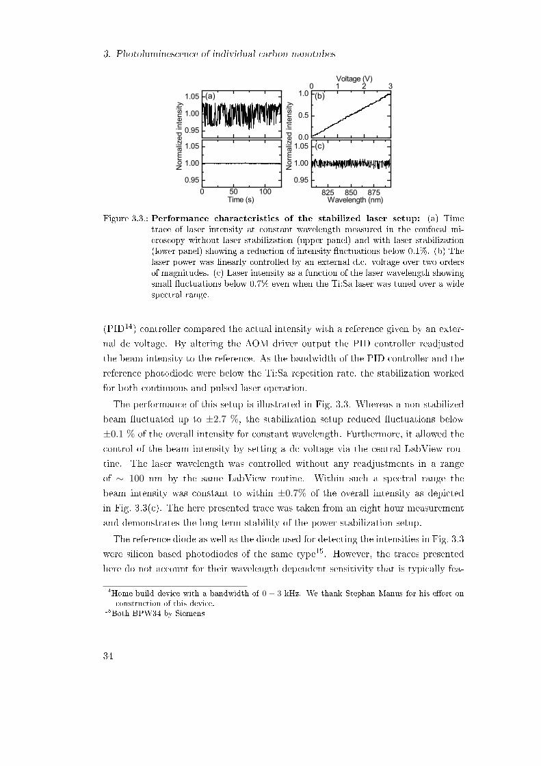
3. Photoluminescence of individual carbon nanotubes
(a) (b)
(c)
825 850 8750.95
1.00
1.05
0.95
1.00
1.05
Nor
mal
ized
inte
nsity
0 50 1000.95
1.00
1.05
Time (s)
0.0
0.5
1.00 1 2 3
Voltage (V)
Nor
mal
ized
inte
nsity
Wavelength (nm)
Figure 3.3.: Performance characteristics of the stabilized laser setup: (a) Timetrace of laser intensity at constant wavelength measured in the confocal mi-croscopy without laser stabilization (upper panel) and with laser stabilization(lower panel) showing a reduction of intensity uctuations below 0.1%. (b) Thelaser power was linearly controlled by an external d.c. voltage over two ordersof magnitudes. (c) Laser intensity as a function of the laser wavelength showingsmall uctuations below 0.7% even when the Ti:Sa laser was tuned over a widespectral range.
(PID14) controller compared the actual intensity with a reference given by an exter-
nal dc voltage. By altering the AOM driver output the PID controller readjusted
the beam intensity to the reference. As the bandwidth of the PID controller and the
reference photodiode were below the Ti:Sa repetition rate, the stabilization worked
for both continuous and pulsed laser operation.
The performance of this setup is illustrated in Fig. 3.3. Whereas a non-stabilized
beam uctuated up to ±2.7 %, the stabilization setup reduced uctuations below
±0.1 % of the overall intensity for constant wavelength. Furthermore, it allowed the
control of the beam intensity by setting a dc voltage via the central LabView rou-
tine. The laser wavelength was controlled without any readjustments in a range
of ∼ 100 nm by the same LabView routine. Within such a spectral range the
beam intensity was constant to within ±0.7% of the overall intensity as depicted
in Fig. 3.3(c). The here presented trace was taken from an eight hour measurement
and demonstrates the long-term stability of the power stabilization setup.
The reference diode as well as the diode used for detecting the intensities in Fig. 3.3
were silicon based photodiodes of the same type15. However, the traces presented
here do not account for their wavelength dependent sensitivity that is typically fea-
14Home-build device with a bandwidth of 0 − 3 kHz. We thank Stephan Manus for his eort onconstruction of this device.
15Both BPW34 by Siemens
34

3.2. Sample preparation and characteristics
tured by semiconductor photodiodes. Nevertheless, in a wide range between 780
and 980 nm the sensitivity of the used photodiodes is reported to vary less than
10 % [119].
Detection devices
We analyzed the collected PL light either spectrally or time-resolved. For recording of
PL spectra we used a commercial spectrometer16, which dispersed the PL light with
a monochromating grating and imaged on a liquid-nitrogen-cooled CCD. Depending
on the used grating of either 300 or 1200 grooves per mm, we reached a spectral
resolution of 220 µeV and 40 µeV, respectively. Since layout and performance of this
spectrometer was reported in detail before [91, 116, 117], it will not be elaborated
here. Devices used for time-resolved measurements, e.g. an Hanbury-Brown-and-
Twiss interferometer, are presented in Chap. 5.2.2.
3.2. Sample preparation and characteristics
This work considers three dierent sample layouts, which provide the CNT with
dierent dielectric environments and dier in the fundamental method of CNT pro-
cessing. Either, the CNTs were commercially available, grown with the use of a
cobalt-molybdenum catalyst (CoMoCat CNTs). Or, they were home-grown in a
chemical-vapor-deposition process with the use of an iron-ruthenium catalyst (CVD
CNTs). Also, CNTs in these samples are either freely suspended in vacuum or em-
bedded in a dielectric medium. And nally, we introduce an external parameter - an
electric eld perpendicular to the CNT axes - to probe for exciton localization, to
determine the perpendicular polarizability of excitons in CNTs, and to switch charge16Acton SP2500 by Princeton Instruments
SiO2
individual CNT
SiSi3
N4
(c)
CVD CNT
(b)
SiO2
NiCr
Al2
O3
Vg
d2
p++- Si
d1
CoMoCat
CNT
SiO2
Si
individualized CNT layer
(a)
CoMoCat
CNT
Figure 3.4.: Sample layouts I: CoMoCat CNTs on a silicon oxide surface, which featuresa metallic grid (a). CoMoCat CNTs embedded in an electric gate device (b).CVD CNT freely suspended over a crater (c).
35

3. Photoluminescence of individual carbon nanotubes
states localized in the dielectric medium. In detail, these layouts are illustrated in
Fig. 3.4. In this chapter, we focus on the rst layout depicted in (a). We stud-
ied commercially available CoMoCat CNTs on a Si-SiO2-substrate, which featured a
lithographically dened metallic grid.
3.2.1. Metallic grid
As a rst step, we dened a grid on an Si-SiO2-substrate. This grid allowed to trace
the respective position of individual CNTs at various temperatures in the confocal
microscopy setup. Furthermore, it enabled the complementary imaging of the same
sample section in dierent imaging devices, e.g. a scanning electron microscope
or an atomic force microscope. The grid consisted of lithographically dened gold
markers each sized ∼ 1 µm. These markers partitioned parts of the sample surface
in 10× 10 µm2 squares each conned by four markers located in the square corner.
The detailed layout is reported in [91] and [117].
3.2.2. CoMoCat material
As a basic source for CoMoCat CNTs we used a commercially available aqueous
CoMoCat CNT solution17, in which the CNTs were dissolved and individualized by
a sodium-cholate (SC) surfactant. Since the CoMoCat method favors the outcome
of certain semiconducting chiralities - namely (6,5) and (7,5) as well as those with
similar diameters -, around 95% of these CNTs show photoluminescence in the near-
infrared spectral range [114]. The detailed recipe for processing a layer of mostly
individualized CNTs on a substrate is documented in Appendix C of this thesis.
In brief, the CNT solution (with an initial density of 1g CNT/l) was diluted in an
aqueous SC solution18 and spun on a cleaned silicon substrate, which was prepared
with a metallic grid as necessary. The density of CNTs on the surface was controlled
via the mixing ratio of the CNT solution and the SC solution. It was typically
adjusted to less than one CNT per µm2. This allowed for individual optical access
with the confocal microscope with a spatial resolution of ∼ 1 µm.
3.3. Spatially resolving imaging techniques
Since it featured a metallic grid, the presented sample design enabled us to retrace
the exact position of a small sample section. First, the grid allowed to record eec-
17SG65 by SouthWest NanoTechnologies, Inc., Norman, OK, USA18Cholic acid sodium hydrates by Sigma-Aldrich Corp.
36

3.3. Spatially resolving imaging techniques
tively the PL spectra of individual CNTs at dierent temperatures, which is focus of
the next Chap. 3.5. Secondly, the grid enabled us to investigate a section using dif-
ferent imaging techniques. Evaluating the respective detection eectiveness of each
imaging technique is a prerequisite, when layers of individualized CNTs need to be
characterized. Since each imaging technique features unique advantages, they were
employed collectively to control and adjust the parameters for processing layers of
individualized CNTs (see previous section 3.2). Thereby, we were able to characterize
layers of individualized CNTs with respect to CNT density (using scanning electron
microscopy and atomic force microscopy), with respect to optical properties (using
photoluminescence microscopy), and with respect to the formation of bundles, which
is mediated by strong van-der-Waals interaction between CNTs (using atomic force
microscopy).
Scanning electron microscopy (SEM) provides for fast imaging of large sample
areas with a medium resolution of ∼ 40 nm. Although this resolution exceeds the
diameter of CNTs (∼ 1 nm), we were able to record a detectable contrast between
CNTs and the Si-SiO2-substrate using a commercially available scanning electron
microscope19 operated with an acceleration voltage of 0.7 kV. In fact, SEM overesti-
mated the CNT diameters by far, but resolved many CNTs in large sample sections
(∼ 100µm2) during a recording time of a few seconds. However, the scanning elec-
tron beam deposits carbon from the ambient residual gas in the microscope chamber.
This deposition gives rise to excessive non-radiative recombination of excitons and
thus quenches all PL. Therefore, we employed SEM only in post-PL imaging and to
adjust the mixing ration of the CNT solutions resulting in a desired CNT density.
Atomic force microscopy (AFM) is a high resolving imaging technique featuring a
height resolution below 1 nm. Thus, it allows to estimate the diameter of individ-
ual CNTs without drawbacks on their optical properties. We used a commercially
available atomic force microscope20 in tapping mode and scanned typically sections
of 2 × 2µm2 with a lateral resolution of 512 pixels in 216 lines. Due to the precise
height resolution we assume that all CNTs in a section could be detected with AFM
imaging. Although AFM is in principle capable of resolving down to the atomic
scale, the use of an unspecied tip precluded to determine the exact diameter of
individual CNTs that were furthermore wrapped in the SC surfactant. Indeed, AFM
enabled us to distinguish between a single CNT and a CNT bundle, but kept us
uncertain about the chirality of a specic CNT. Further, this technique is very time
19eLine by Raith GmbH, Germany20Nanoscope 3100 by Digital Instruments now Bruker Corporation MA, USA
37

3. Photoluminescence of individual carbon nanotubes
1 µm
(a) (b) (c)
Figure 3.5.: Complementary imaging of the same sample area of 10× 10 µm2 using (a)scanning electron microscopy, (b) atomic force microscopy, and (c) spatiallyresolved PL microscopy.
consuming. For instance, recording of the section depicted in Fig. 3.5(b) took more
than 7 hours. We used AFM routinely to check in spot tests layers of individualized
CNTs with respect to CNT density and formation of CNT bundles. In addition,
AFM allowed to adjust the mixing ratio of the SC surfactant in the CNT solution.
Spatially resolved PL microscopy was accessible with our microscopy setup at var-
ious temperatures (T = 300 K, 77 K, 4.2 K). To record a spatially resolved map
a sample section was scanned point by point while recording a spectrum at every
coordinate point with a xed excitation wavelength, intensity and (circular) polar-
ization. Reproducible positioning of the sample was facilitated by the use of the
lateral scanning unit (see Chap. 3.1.1). In contrast to the stepping units, it contin-
uously positioned the sample with reference to an external voltage. In this scheme,
hysteresis eects and long term drifts were kept well below the spatial resolution of
the confocal microscope [120]. We set the distance between two coordinate points
typically with 0.5 µm, which was half of the microscope resolution of 1 µm. Although
this technique is time consuming, it reveals the optical properties of the CNTs lo-
cated in the sample section. In contrast to the other imaging techniques, spatially
resolved PL microscopy reveals only CNTs that show PL in a limited spectral range.
Many others stay dark, like metallic CNTs, CNTs with a too low (big) band gap, or
CNTs with quenched PL emission.
The diploma thesis of M. Hofmann included a detailed comparative study [91],
which revealed the eectiveness of these imaging techniques. Samples with a metallic
grid allowed to record the same sample sections with all three imaging technique.
Exemplarily, a 10 × 10 µm2 sized section is shown in Fig. 3.5. The bright patterns
in the left corners are part of the metallic grid. The SEM image, which is depicted
in Fig. 3.5(a), features individual CNTs as white lines. The similarity to the AFM
38

3.4. Signatures of individual CoMoCat CNTs
image (b) is particularly apparent for the triangle constellation of three CNTs below
the upper metallic pattern on the left image border and for the single long tube in
the middle slightly above the lower image border. Compared to the PL map taken
at T = 4.2 K both areas showed also bright PL intensity.
Due to its outstanding height resolution, AFM images can be taken as a reference
for the total number of CNTs located in a sample section. By comparison with
the other imaging techniques we nd that approximately 80% of the CNTs showed
a detectable contrast to the substrate in SEM images. Around 70% of the CNTs
showed PL in the spectral range (900-1020 nm). This is in good agreement with the
estimated share of 95% semiconducting CNTs resulting from the CoMoCat growth
process21. However, the PL emission of some of these CNTs was not included in the
observed spectral range - as is the case for the (7,6) chirality, which typically emits
at 1120 nm [88] and makes up around ∼ 10% of all CoMoCat CNTs [114].
In summary, we have established a procedure to form a layer of individualized
CNTs on a Si-SiO2 substrate. The use of complementary imaging techniques allowed
us to adjust eectively the mixing ratios for the CNT solution and other processing
parameters. The density of CNTs was well-adjusted to ensure exclusive access to
individual CNTs with a confocal microscope, whose spatial resolution was close to
the diraction limit. This lays the foundation for optical spectroscopy of individual
CNTs.
3.4. Signatures of individual CoMoCat CNTs
The PL of individual CNTs was rst reported independently by Lefebvre et al. [27]
and Hartschuh et al. [26]. They revealed several signatures of individual CNTs that
dier from those of CNT ensembles: Namely, single (asymmetric) emission peak at
cryogenic temperature and highly polarization dependent absorption and emission
due to the antenna eect (see Chap. 2.2.3).
Whenever we scanned the sample laterally for searching individual CNTs, we used
a circularly polarized, cw excitation beam while shifting the sample through the
focal spot in lateral steps with the piezo positioners. However, we had only limited
information about the present microscopic formation of CNTs in the focal spot.
Unless we would employ other imaging techniques, much remained unclear like the
exact number of CNTs, whether these formed bundles or whether they were metallic
or semiconducting with untting band gap or quenched PL. However, we could rule
21Compare to data sheet of SG65 CNTs or Ref. [114].
39

3. Photoluminescence of individual carbon nanotubes
out these objection by processing properly the layer of individualized CNTs. This
included the use of a SC surfactant that individualized the CoMoCat CNTs and
prevented them from forming bundles [104]. Plus, we adjusted the density on the
substrate below one tube per µm2. In addition, we focussed on sample sites, which
showed unambiguous spectral PL response as we will discuss here and in Chap. 4.4.
The spectral range of interest was limited by the used long-pass lter and by the
chromatic aberration of the confocal microscope that narrowed the range to ∼ 50 nm.
Thus, our view was respectively concentrated on a few CNT chiralities22 that emit
within this range (see Kataura plot Fig. 2.5).
As exemplied in Fig. 3.6(b), we found single emission peaks, whose intensity
typically exceeded other background emission (that consisted of Raman emission
from the CNT but dominantly from the silicon substrate) by at least a factor of
100. These were laterally conned and intensied particularly when the sample was
positioned vertically in the focal plane. The background was mostly composed of a
characteristic Raman signal that we assigned to originate from the silicon substrate.
This signal was observed independently from the lateral position and, in contrast
to CNT PL signals, was also very robust against variations of the sample's vertical
positioning to the focal plane. At cryogenic temperature (T=4.2 K) the recorded
PL peaks were predominantly asymmetric with a steep edge on the high-energy side
and a smoother fall to low energy. Fitting a Lorentzian peak showed good agreement
22Namely, in the range from 860 to 1000 nm PL emission is expected from the chiralities (6,2),(6,4), (6,5), (7,0), (7,3), (8,3) and (9,1). Their diameter varies from 0.56 to 0.78 nm.
180°
270° 90°
1.30 1.35 1.40
0
20
40
Inte
nsity
(cts
s-1µW
-1)
PL energy (eV)
0°(b) (c)(a)
Figure 3.6.: Photoluminescence of a single carbon nanotube: (a) A single CNT im-aged by AFM. The scale bar measures 500 nm. (b) Excited continuously bya linearly polarized laser beam with λexc = 845 nm an individual CNT showsa single asymmetric emission line. Whereas a Lorentzian peak (solid line) isunable to reproduce the emission peak's asymmetry it gives reliable measures ofthe central PL energy and the peak width. (c) Normalized PL intensity (radialdegree on a linear scale) as a function of the linear polarization angle ζ (relativeto the CNT axis). The solid line displays a cos2 t.
40
3.5. Exciton localization at low temperatures
with the low-energy edge, but did not reproduce the high-energy slope. Nevertheless,
it provided a reliable measure for the PL central energy EPL, the peak width Γ and
the PL intensity I. For investigation of the asymmetry we split a PL peak around
the central PL energy into two halves, which can be each reproduced by an halved
Lorentzian peak. This procedure is discussed in the following Chap. 3.5.
Further, individual CNTs showed a pronounced antenna eect with a high aspect
ratio (∼ 50 : 1) between intense emission for the excitation polarization being parallel
to the tube axis and vanishing PL emission for perpendicular excitation. As depicted
by the solid line in Fig. 3.6(b) the intensity followed a cos2 ζ, where ζ denotes the
angle between excitation polarization axis and the tube axis.
A denite proof that an emission site is due to an individual CNT can only be
shown by the detailed analysis of its photon statistic. As we will discuss in Chap. 5,
we have successfully performed such measurements on substrate supported CNTs.
Without any exception, all of them showed photon anti-bunching, which excluded
the presence of a second (identical) CNT in the focal spot.
In summary, samples with layers of individualized CNTs, which we controlled
eectively by complementary imaging techniques, showed clear evidence of PL from
individual CNTs (single asymmetric peaks, antenna eect, photon anti-bunching).
As a synopsis of the here presented experimental results, interaction of an individual
CNT with neighboring CNTs (like in bundles) can be regarded as precluded.
3.5. Exciton localization at low temperatures
Whereas the previous considerations focussed merely on methods for processing and
characterizing layers of individualized CNTs, we now turn to the optical properties
of individual CNTs at various temperatures. Previously reported experiments [60,
76, 121] traced the PL signal of only a single individual CNT while changing the
temperature. Thus, the sample must be cooled-down and warmed repetitively to
achieve a signicant number of spectra from several individual CNTs. However,
every change of temperature includes the risk that the sample might detach from
the piezo positioners or that the piezo positioners freeze. In contrast, samples with
metallic grids enabled us to record a number of PL maps at 4.2 K and then repeated
this at 77 K and 300 K, which required only one temperature iteration. In analysis of
these maps, we concentrated on sites, which showed a single asymmetric emission line
at 4.2 K. Fig. 3.7(a) illustrates the main characteristics of a PL spectrum recorded
41
3. Photoluminescence of individual carbon nanotubes
at various temperatures: a broadening of the line width towards a symmetric line
shape and a shift of the central PL emission energy [60].
As we will discuss now, both features can be traced back to the localization of
excitons at cryogenic temperatures [122]. Before recombination excitons probe ten
thousands of CNT lattice sites during their diusion, so that the PL signal of CNTs
was identied as particularly sensitive to environmental uctuations and bonding of
individual ad-atoms to the CNT [73, 123, 124]. During diusion excitons experience
variations in the energy landscape, which can result in localization of excitons and
formation of bright emission sites along a CNT [58]. Typically, such sites show PL
emission with an energy shifted to the red by several 10 meV [125]. The localization of
excitons was also revealed by analyzing the ultra-fast dynamics of exciton generation
and decay [126]. In addition, the localization of excitons is purposefully responsible
for the asymmetric PL emission line shape [59] and the quantum dot like photon
emission of cryogenic CNTs [76,77,127].
We begin with the analysis of the PL line shape. Its asymmetry has been identied
as a fundamental property of the PL from individual CNTs at lowest temperatures,
whereas the line shape becomes symmetric at higher temperatures of T = 77 K and
beyond [60, 121]. As exemplied in Fig. 3.7(a), we observed an analogous behavior
within our experiments. To quantify the line shape of a PL peak, we used a simple
asymmetric peak function, which was composed of two halved Lorentzians23 each
featuring a dierent width (full width half maximum). The half on the blue side
exhibited a steep width Γ, whereas the half on the red was additionally broadened
by Γasy. The total width of this asymmetric peak was given by Γ+Γasy. As depicted
by the blue solid line in Fig. 3.7(b), this asymmetric peak function reproduced the
PL spectra of individual CNTs at T = 4.2 K.
The broadening of the line width as a function of the temperature Γ(T ) has been
investigated by Yoshikawa et al. [121]. Since these studies covered only temperatures
ranging from 40 K to 300 K, the line shapes were predominantly symmetric. In
agreement with these studies, we nd Γ following a model [128] that considers exciton
23The Lorentzians are halved around the central PL energy EPL. The asymmetric peak functionis dened as
I(E) =
2I0(Γ+2Γasy)
π
Γ+2Γasy
4(E−EPL)2+(Γ+2Γasy)2, for E < EPL
2I0Γπ
Γ4(E−EPL)2+Γ2 , for E ≥ EPL .
(3.1)
Here, I0 denotes the intensity. Γ is the symmetric part of the line width, whereas Γasy denotesthe asymmetric part. The total line width is then given by Γ + Γasy.
42
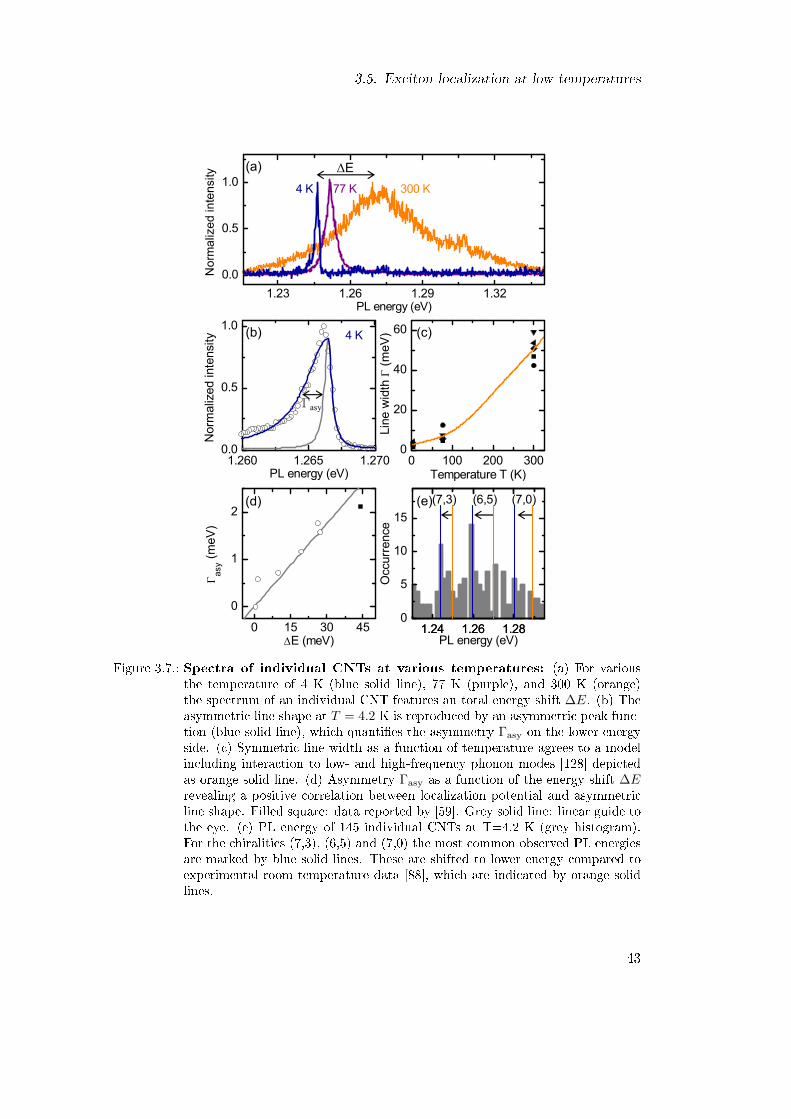
3.5. Exciton localization at low temperatures
(a)
(b) (c)
(d) (e)
ΔE
Γasy
0.0
0.5
1.0 4 K 77 K 300 K
1.23 1.26 1.29 1.32
Nor
mal
ized
inte
nsity
PL energy (eV)
0 100 200 3000
20
40
60
Line
wid
th Γ
(meV
)
Temperature T (K)1.260 1.265 1.270
0.0
0.5
1.04 K
Nor
mal
ized
inte
nsity
PL energy (eV)
0 15 30 45
0
1
2
Γ asy (m
eV)
ΔE (meV)1.24 1.26 1.28
0
5
10
15
Occ
urre
nce
PL energy (eV)1.24 1.26 1.28
(6,5) (7,0)(7,3)
Figure 3.7.: Spectra of individual CNTs at various temperatures: (a) For variousthe temperature of 4 K (blue solid line), 77 K (purple), and 300 K (orange)the spectrum of an individual CNT features an total energy shift ∆E. (b) Theasymmetric line shape at T = 4.2 K is reproduced by an asymmetric peak func-tion (blue solid line), which quanties the asymmetry Γasy on the lower energyside. (c) Symmetric line width as a function of temperature agrees to a modelincluding interaction to low- and high-frequency phonon modes [128] depictedas orange solid line. (d) Asymmetry Γasy as a function of the energy shift ∆Erevealing a positive correlation between localization potential and asymmetricline shape. Filled square: data reported by [59]. Grey solid line: linear guide tothe eye. (e) PL energy of 145 individual CNTs at T=4.2 K (grey histogram).For the chiralities (7,3), (6,5) and (7,0) the most common observed PL energiesare marked by blue solid lines. These are shifted to lower energy compared toexperimental room temperature data [88], which are indicated by orange solidlines.
43

3. Photoluminescence of individual carbon nanotubes
coupling to low- and high-frequency phonon modes
Γ = Γ0 +A T +B1
e~ωphononkBT − 1
. (3.2)
In this model the parameter A measures the coupling to low-frequency phonon
modes, whereas B gives the coupling to high-frequency phonon modes. The energy
of the high-frequency phonon modes is termed as ~ωphonon. When this model is
applied to our ndings as indicated by the orange solid line in Fig. 3.7(c), A =
(0.05± 0.04) meV/K agrees with the previously reported value of 0.03 meV/K [121].
In contrast to Yoshikawa's report, the interaction with high frequency phonon modes
can not be neglected because our experiments covered a broader temperature range.
Considering only interaction to the radial breathing mode (RBM), we nd B =
(141± 41) meV/K.
Γasy quantied the peak asymmetry and ranged typically from 0.04 meV to 1.8 meV
with an mean value of (0.4 ± 0.1) meV at T = 4.2 K. We observed for some emis-
sion peaks a Γasy that exceeded Γ up to a factor 150 at T = 4.2 K, whereas the
asymmetric part became insignicant Γasy < 0.22Γ for all investigated CNTs at
room temperature. As origin of the asymmetry at cryogenic temperature Galland
et al. [59] proposed a model based exciton-phonon coupling of localized excitons.
They evaluated localization potentials on the scale of a few 10 meV and associated
explicitly an asymmetry of Γasy = 2.1 meV with a localization potential of 44 meV.
Although their model allows to describe the asymmetry of CoMoCat CNTs at cryo-
genic temperatures, it fails to understand the ultra-narrow emission of suspended
CVD CNTs, which are highly isolated from their environment (discussed in Chap. 5).
Thus, we will not evaluate the localization potential in their terms. Rather, we will
use a dierent measure to quantify the localization potential. This is termed as ∆E
and quanties the apparent energy shift on the PL energy, when the temperature is
increased
∆E = EPL(T = 300 K)− EPL(T = 4.2 K) , (3.3)
which is also depicted in Fig. 3.7(a). For all investigated CNTs, this shift was positive
between 0.4 meV up to 27.3 meV indicating a generally reduced PL emission energy
at cryogenic temperature. As illustrated in Fig. 3.7(d), we were able to nd a positive
correlation between this energy shift ∆E and the asymmetry Γasy. This correlation
coincides with Galland's report, which is marked as black lled circle in Fig. 3.7(d).
44
3.5. Exciton localization at low temperatures
Analogous to Galland's proposal this correlation suggests that the asymmetry of the
PL emission peak and the energy shift have the same physical origin.
Furthermore, we identied energy shifts on the same order of magnitude by con-
sidering the distribution of the PL energies of 145 CNTs recorded at T = 4.2 K as
illustrated in the histogram in Fig. 3.7(e). For the most frequent CNT chiralities
(6,5), (7,0) and (7,3) this histogram displays solid orange lines, which indicate room
temperature values of the PL energy of CoMoCat CNTs reported by Weisman et
al. [88]. In addition, blue solid lines indicate the most common PL energies observed
within our experiments at T = 4.2 K. Comparing both lines, the distribution of
the PL energy at cryogenic temperature can be interpreted as generally reduced by
60, 105 and 85 meV for (7,3), (6,5) and (7,0) CNTs, respectively (black arrows).
Although Weisman's report considers CNTs with SDS surfactant, only ∼ 5 meV of
the redshift results from the dierent surfactant [129]. If we furthermore account
for the dielectric SiO2 substrate with a dielectric constant of ε = 3.9, environmen-
tally induced redshifts were not reported to exceed 49 meV [106, 130]. Thus, the
vast majority of cryogenic CoMoCat CNTs featured an PL energy that was several
10 meV lower than expected. This energy scale agrees with the energy shift ∆E as
well as with the localization potential observed by Galland et al. [59] in the context
of localized excitons interacting with phonons. It is further in accordance with the
reduced PL energy of localized excitons directly observed by Georgi et al. [125].
Several alternative mechanisms for temperature induced variation of the PL energy
of pristine CNTs are reported. First, a higher temperature increases the carbon-
carbon bond length acc resulting in a smaller overlap integral γ0 (see Chap. 2.2) and
thus a smaller band gap. This was conrmed theoretically [54] and experimentally
[60]. Applied to our experiments, this mechanism would result in an higher PL energy
at cryogenic temperature. Secondly, axial strain varies the CNT band-gap [131]
causing family selective shifts of the PL energy to the red or the blue. However, for
all the here considered chiralities24 strain induces shifts only to the blue, which do
not exceed a few meV [132]. So, both mechanisms would manifest in an increased
PL energy for cryogenic temperatures, which contradicts the here observed energy
shifts to lower PL energies.
In summary, we have identied several indication for the localization of excitons in
CNT quantum dots at cryogenic temperatures. These are asymmetric emission peaks
at low temperature, which has been purposed to originate from the localization of
excitons [59]. This comes along with a reduction of the PL energy on the scale of a few
24(6,5), (7,0) and (7,3) belong to the same family.
45

3. Photoluminescence of individual carbon nanotubes
∼ 10 meV that agrees with typical localization potentials of localized excitons [58]. A
correlation between the magnitude of the localization potential and the asymmetry
of an emission prole indicates that both phenomena have the same physical origin.
Thus, our ndings can be interpreted by the localization of excitons in CNT quantum
dots at cryogenic temperatures. Since these traps measure a few 10 meV, excitons are
presumably unable to overcome these localization potentials and recombine mostly
from conned emission sites (CNT quantum dots). Not before their energy is on same
order of magnitude - as it is the case for room temperature (kB 300 K ≈ 26 meV) -
excitons delocalize, which becomes apparent in symmetric emission peaks with a PL
energy matching to the CNT band-gap.
A nal remark should regard the excitation laser. As we will discuss in Chap. 4.7
localized exciton states can be generated by pumping via higher harmonics of the
trapping potential. Tuning the excitation laser to (phonon-)sidebands slightly above
the E11 energy gap, could increase the creation of localized exciton states and would
make the search for CNTs highly selective to such CNTs that feature exciton local-
ization. This could explain, why experiments using excitation via sidebands face
asymmetric PL line shapes [59,133] and photon anti-bunching [76,77,127] indicating
for localization of excitons. In contrast, experimentalists using excitation via the E22
electronic states reported mostly on symmetric emission lines [60,73,121].
46

4. Tuning the photoluminescence with
electric elds
We investigated the PL of cryogenic CoMoCat CNTs as a function of a
perpendicularly applied electric eld. Prior spectral classication allowed
to distinguish between two CNT types [134]: The rst consisted of indi-
vidual CNTs showing a single asymmetric emission peak. As a function
of the electric eld the PL energy of these CNTs was shifted to the red,
which was mediated by the perpendicular polarization of excitons [82,135].
Within our experiments, the energy of both lines was shifted linearly as a
function of the applied electric eld. We interpret our ndings that CNTs
of the second type featured a permanent dipole moment that arose from
impurities induced breaking of the CNT symmetry.
As a third characteristic, CNTs featured a reversible emergence of an
additional satellite peak. In favor of the satellite intensity the intensity of
the bright exciton emission line was systematically quenched as a function
of the applied electric eld. The energy splitting of this satellite peak to
the bright exciton line agrees with experimental [4749] and theoretical
[55,81] values of the charged exciton (trion) splitting. Thus, our ndings
can be interpreted with the generation of trions by eld induced doping
of CNTs.
In addition to the homogenous electric eld, switching of charge states
in the dielectric medium close to a CNT altered an inhomogenous elec-
tric eld. Controlled by the gate voltage inhomogenous electric elds
systematically tuned the localization potential of excitons in individual
CNTs [62]. Using photoluminescence excitation spectroscopy [136] we
identied that the harmonic excitation spectrum of a CNT quantum dot
featured signatures of a phonon bottleneck in the relaxation of excited
exciton states [137].
47

4. Tuning the photoluminescence with electric elds
4.1. Electric eld structure
In order to study optical properties of individual CNTs as a function of an exter-
nal electric eld, we fabricated a metal-oxide-semiconductor (MOS) capacitor device
sketched in Fig. 4.1(b). Applying a dc gate voltage (Vg) between its top and back
gates generates a homogeneous electric eld perpendicular to the CNT axis regard-
less of their orientation on the substrate. To provide for high electric elds, the
insulating layers should exhibit a high dielectric strength. As required for ecient
PL spectroscopy of CNTs such a device must exhibit (semi-) transparent layers and
must be functional at cryogenic temperatures.
SiO2
individual CNT
SiSi3
N4
(c)
CVD CNT
(b)
SiO2
NiCr
Al2
O3
Vg
d2
p++- Si
d1
CoMoCat
CNT
SiO2
Si
individualized CNT layer
(a)
CoMoCat
CNT
Figure 4.1.: Sample layouts II: (a) CoMoCat CNTs on silicon oxide surface, which featuresa metallic grid. (b) CoMoCat CNTs embedded in an electric gate device. (c)CVD CNT freely suspended over a crater.
For fabrication of such a MOS capacitor, we started with a layer of individualized
CNTs on a Si-SiO2 substrate considered previously in Chap. 3.2. Since the silicon
substrate was highly doped, it exhibited a sucient electric conductance to act as
back gate. The CNTs were insulated from the back gate by the dielectric SiO2
lm. To complete the gate structure a second insulating layer (here aluminium oxide
Al2O3) and a semi-transparent metallic top gate (nickel chromium NiCr) were re-
quired. As characteristic MOS capacitor, the device exhibited a capacitance-voltage
prole (CV) that was dominated by the creation rate of charge carriers in the semi-
conducting back gate and by oxide charge states within the insulating layers.
4.1.1. Growth and characterization of thin lms
Silicon oxide
We used highly p++-doped silicon wafers1 (boron dopant) polished on both sides as a
substrate material for all devices. The room temperature resistivity was measured to
1Acquired from Wacker AG with special thanks to P. Stallhofer
48

4.1. Electric eld structure
be 5− 10 mΩ cm−1 - equivalent to a dopant concentration of 1− 2 · 1019 cm−3 [138].
The thickness of the thermal silicon oxide lm (SiO2) measured d1 = 100 nm and
was not altered for dierent sample layouts presented. For further processing the
wafer was cut into pieces of 7 × 7 mm2. On top a layer of individualized CoMoCat
CNTs was processed according to methods documented in Appendix C.
Aluminium oxide
Thin aluminum oxide (Al2O3) lms exhibit a high dielectric strength, which are
reported to exceed 107 V/cm [139]. Additionally, Al2O3 acts as a barrier for mobile
sodium ions. These typically contaminate SiO2 lms and play a central role in the
breakdown of pure SiO2 capacitors [140]. Thus, Al2O3 complements ideally to SiO2
lms for fabrication of thin lm capacitors. Furthermore, Al2O3 is transparent in
the visible and near infrared and thus ideal for optical applications.
We deposited Al2O3 lms by electron beam evaporation in a high-vacuum cham-
ber. During the growth process, a quartz microbalance monitored deposition rate
(typically 1 Ås−1) and lm thickness. Although this microbalance granted for com-
parable control of the deposition parameters, it generally underestimated the oxide
thickness by ∼ 30%. More reliable results for the oxide thickness were obtained with
ellipsometry measurements2. The values measured with this method were in accor-
dance with two other methods used for the determination of the oxide thickness.
Firstly, the thickness of the oxide layers were evaluated from the capacitance of the
MOS capacitor. Secondly, the color of thin oxide lms is governed by the refractive
index n and the lm thickness d. Color tables for thin SiO2 lms as a function
of their thickness are summarized in Ref. [138]. We adopted them to Al2O3 using
nAl2O3 · dAl2O3 = nSiO2 · dSiO2 .
This thesis presents experimental data measured on four dierent MOS capacitor
devices with dierent thickness of the Al2O3 lm d2(' 7 nm, 17 nm, 39 nm and
42 nm).
Nickel chromium
In order to excite CNTs within the gate device and to detect their PL signal the
top gate has to be transparent in the near-infrared spectral range. Ideal materials
for the top gate would be indium-tin-oxide (ITO) [141] or a mono-layer graphene
ake [142]. Alternatively, thin metallic lms of nickel chromium (NiCr) lms can be
used [116]. These are easy to fabricate and semi-transparent in the near infrared.2PC 2300 by Plasmos GmbH, Germany
49

4. Tuning the photoluminescence with electric elds
(a) (b)
0 5 100.1
0.5
1
Tran
smis
sion
NiCr thickness (nm)
d0=(4.7±0.5)nm
0
1
Inte
nsity
(a.u
.)-1.0 -0.5 0.0 0.5 1.0
Position (mm)
Figure 4.2.: Fabrication of a semi-transparent top gate: (a) Transmitted (orangetrace) and reected (blue trace) intensity as a function of the laser spot po-sition. The range within ±0.5 mm was covered with a NiCr lm. (b) Transmis-sion coecient as a function of the NiCr lm thickness. The solid orange linerepresents an exponential decay t of Lambert-Beer's law.
We deposited a thin layer of NiCr as a top gate by thermal evaporation in a
high-vacuum chamber. The deposition rate was controlled by a quartz crystal mi-
crobalance and usually set to 1 Ås−1. We used shadow masks to dene the shape of
the top gate with an area of 4.6 mm2 centered on the substrate piece. After depo-
sition we checked the lm thickness by ellipsometry. Ellipsometry measurements on
composites of NiCr and Al2O3 lms on Si-SiO2 substrates were reported by Ohlidal
et al. [143].
The ideal NiCr thickness is a trade-o between light absorption and electric bulk
conductivity. Fig. 4.2 summarizes the transmission coecients for NiCr lms with
various thickness measured at 960 nm. Applying the Lambert-Beer law [144], we nd
a half-value thickness d0 = (4.7± 0.5) nm. Further, we performed measurements of
the electrical dc resistance on test samples. We did not observe any deviations from
a bulk conductor and found a constant resistivity for all lms thicker than 2.0 nm.
For all MOS devices considered in this thesis the NiCr thickness was between 2.0
and 4.5 nm.
4.1.2. Ohmic contacts
In order to apply a voltage between the NiCr lm (top gate) and the highly doped
silicon substrate (back gate) both were contacted to a voltage source. Contacting
a thin metallic wire to the semiconducting back gate could result in a junction
dominated by a Schottky barrier [145] whereas the junction between a metallic wire
and the metallic top gate was not subject to this diculty. Such non-ohmic behavior
would inhibit a reasonable operation of the device especially at low temperatures.
50
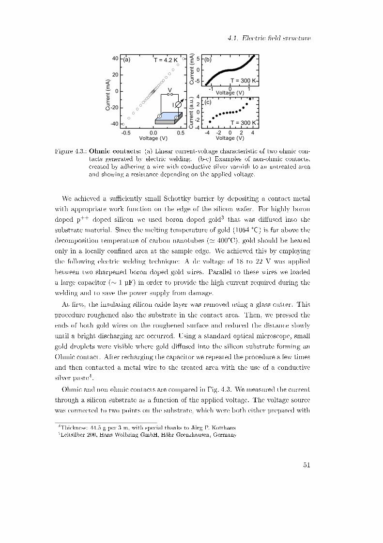
4.1. Electric eld structure
-4 -2 0 2 4-4-2024
-0.5 0.0 0.5
-40
-20
0
20
40
Cur
rent
(mA)
Voltage (V)
-1 0 1-5
0
5
Cur
rent
(mA)
Voltage (V)
Cur
rent
(a.u
.)
Voltage (V)
(a) (b)
(c)
V
I
1 2
T = 4.2 K
T = 300 K
T = 300 K
Figure 4.3.: Ohmic contacts: (a) Linear current-voltage characteristic of two ohmic con-tacts generated by electric welding. (b-c) Examples of non-ohmic contacts,created by adhering a wire with conductive silver varnish to an untreated areaand showing a resistance depending on the applied voltage.
We achieved a suciently small Schottky barrier by depositing a contact metal
with appropriate work function on the edge of the silicon wafer. For highly boron
doped p++ doped silicon we used boron doped gold3 that was diused into the
substrate material. Since the melting temperature of gold (1064 °C) is far above the
decomposition temperature of carbon nanotubes (' 400°C), gold should be heated
only in a locally conned area at the sample edge. We achieved this by employing
the following electric welding technique: A dc voltage of 18 to 22 V was applied
between two sharpened boron doped gold wires. Parallel to these wires we loaded
a large capacitor (∼ 1 µF) in order to provide the high current required during the
welding and to save the power supply from damage.
At rst, the insulating silicon oxide layer was removed using a glass cutter. This
procedure roughened also the substrate in the contact area. Then, we pressed the
ends of both gold wires on the roughened surface and reduced the distance slowly
until a bright discharging arc occurred. Using a standard optical microscope, small
gold droplets were visible where gold diused into the silicon substrate forming an
Ohmic contact. After recharging the capacitor we repeated the procedure a few times
and then contacted a metal wire to the treated area with the use of a conductive
silver paste4.
Ohmic and non-ohmic contacts are compared in Fig. 4.3. We measured the current
through a silicon substrate as a function of the applied voltage. The voltage source
was connected to two points on the substrate, which were both either prepared with
3Thickness: 44.5 g per 3 m, with special thanks to Jörg P. Kotthaus4Leitsilber 200, Hans Wolbring GmbH, Höhr-Grenzhausen, Germany
51

4. Tuning the photoluminescence with electric elds
(a) or without (b-c) gold contacts. For the gold treated samples we found ohmic
junctions with a linear current-voltage characteristic even at a temperature of 4.2 K.
In contrast, the contact resistance of an untreated sample revealed a non-ohmic
behavior even at room temperature.
4.2. Capacitance-voltage characterization
The rst part of the following section gives a brief theoretical overview on the elec-
trical properties of an ideal MOS device. Then, we present capacitance-voltage (CV)
measurements on our MOS capacitor samples. Knowing the CV characteristic of a
device allowed to evaluate the electrostatic eld through the layer of individualized
CNTs. On a microscopic level this eld was not only dominated by the homoge-
nous electric eld generated between the biased top and back gate capacitor plates.
Rather, an additional inhomogeneous electric eld arose from oxide charge states
located in the dielectric medium close to the CNT layer. From comparative mea-
surements of devices with dierent layer geometry we evaluated the oxide charge
density in the MOS capacitor device.
4.2.1. Ideal MOS capacitor
The ideal MOS device is not an ideal parallel-plate capacitor [138]. Rather, its
CV characteristic is dominated by the semiconducting nature of the back contact.
Particularly, the generation rate of charge carriers within the semiconductor contrasts
mainly to a metal-plate capacitor. Fig. 4.4(a) depicts the density of charge carriers
Qs as a function of the surface potential φs (that is not identical to the applied gate
voltage Vg!) for a p-type semiconductor. For reverse bias φs < 0, accumulation of
majority charge carriers provides for a metal-like charging characteristic. For small
forward bias, the majority carriers are depleted from the semiconductor surface. The
width of the depletion region is denoted by xd. Since there are no minority carriers
available, the intrinsic Fermi level Ei is still above the Fermi energy EF . Only when
Ei is bent below EF , forward biasing gives rise to the accumulation of minority
carriers also referred to as inversion.
In the following, we briey present the calculations by Grove et al. [146] for a
p-type MOS capacitor. These are also summarized in the standard textbook on
semiconductor physics by Sze [138], which elaborates particularly on the eects of
charge states. We followed these calculations to relate the applied gate voltage Vg to
52

4.2. Capacitance-voltage characterization
the strength of the created homogeneous electric eld F . Furthermore, we determined
the average density of oxide charge states QOT in the surrounding of the CNT layer.
In general, the capacitance of a MOS device can be regarded as a series connection
of the oxide capacitance5 Co, which is the capacitance of a parallel plate capacitor
with identical dimensions Co = εε0/d, and the dierential or space charge capacitance
Cs accounting for all eects due to the semiconducting nature of the back gate
1
C=
1
Co+
1
Cs. (4.1)
In thermodynamic equilibrium, the carrier concentration of electrons and holes within
the semiconductor is given as a function of the surface potential φs by
p = ni exp(uF − us) (4.2)
n = ni exp(us − uF ) (4.3)
where we dene the relative potentials us = qφs/kBT and the intrinsic carrier con-
centration ni. At T = 300 K, ni(300 K) is given by n0i = 1.45 · 1010 cm−3. For
other temperatures ni scales with T 3/2 exp (Eg/kBT ). The relative Fermi potential
φF depends on the dopant concentration only. For a p-type semiconductor the bulk
density of acceptors NA exceeds the density of donors ND. Thus, the Fermi level is
shifted towards the valence band and we can write for the Fermi potential
2ni sinhuF = q(NA −ND) > 0. (4.4)
Solving the Poisson equation yields the total net charge density Qs within the semi-
5In accordance with Ref. [138,146] C denotes here the capacitance per area given in units of F/cm2
1011 1012 1013 1014 101510-3
10-2
10-1
-1.0 -0.5 0.0 0.5 1.0 1.5
1013
1015
1017
1019
|QS/q
| (cm
-2)
φS(V)
x d(µm
)
|QS/q| (cm-2)
(a) (b)
acc d wi si
Figure 4.4.: Charge density Qs and depletion width xd calculated for the given sampleparameters at Teff = 324 K. (a) Qs as a function of the surface potential φs
showing accumulation (acc), depletion (d), weak (wi) and strong inversion (si).(b) Depletion width xd saturates when weak inversion sets in.
53

4. Tuning the photoluminescence with electric elds
conductor as shown by Kingston et al. [147]. So, Qs is expressed as a function of the
surface potential φs and reads as
Qs = −2us|us|
qniLD√
2[cosh(us − uF )− cosh(uF ) + us sinhuF ] (4.5)
with the Debye length LD dened by
LD =
√kBTεsε0
2q2ni. (4.6)
Here, kB denotes the Boltzmann constant, q the elementary charge and εs the dielec-
tric constant of the semiconductor. Fig. 4.4(a) depicts the number of charge carriers
|Qs/q| as a function of the surface potential φs. For large forward (φs 0) and
reverse (φs 0) bias, it shows a metal like exponential increase, which results in
strong inversion (si) and accumulation (acc) of holes, respectively. Around zero bias,
|Qs/q| increases only slightly in the depletion (d) and saturates for weak inversion
(w) due to the lack of electrons.
Generation of minority carriers
At equilibrium, the space charge capacitance Cminoritys is given by the derivative of
the charge density Qs with respect to φs. Using Eq. (4.5), we nd
Cminoritys = εsε0
q(p− n+ 2ni sinhuF )
Qs. (4.7)
Domination of majority carriers
However, the situation is dierent when there is only an insucient density of mi-
nority carriers available. This is the case for high modulation frequency or at low
temperature. Here, the CV characteristics is solely governed by majority carriers and
their depletion, which sets in at small forward biasing. The width of the depletion
region xd is dened by
xd =Qs
q(ND −NA), (4.8)
which is the ratio of the surface charge density Qs to the uniform doping (bulk)
density ND−NA. Knowing the dopant concentration, xd can be evaluated explicitly
with use of Eq. (4.5). For the given material properties of our devices, Fig. 4.4(b)
plots xd as a function of the surface potential φs. The depletion width xd saturates
54

4.2. Capacitance-voltage characterization
when the charges in the depletion region screen completely the electric eld from
the semiconductor. Hence, the resulting space charge capacitance Cmajoritys is only
determined by xd and reads as
Cmajoritys =
εsε0xd
. (4.9)
Charge states
The used MOS devices diered from the above considered ideal CV curve in several
points. Charge impurities were the most dominant dierence. On a microscopic
level, an individual CNT was subject to the inhomogeneous electric eld of charge
states in addition to the homogenous electric eld generated by the charged gates.
However, CNTs were only aected by neighboring charge states located in the dielec-
tric medium whereas they were insensitive to charge states on the Si-SiO2 interface.
The latter resulted from open silicon bonds and are termed as interface trap charges.
Their surface density is here denoted as QIT. In contrast, volume states ranged over
the entire dielectric medium and originate from oxide trap charges6. The density of
these oxide charge states is given by QOT. Thus, we can state the total density of
charge states Qtot as the sum of the interface charge density and the oxide charge
density
Qtot = QIT +QOT . (4.10)
Gate voltage Vg as a function of the surface potential φs
Up to now we considered all relations as a function of the surface potential φs. In
experiments however, only the gate voltage Vg applied between top and back gate
was controllable. This applied voltage is enhanced by the work function dierence
between the metallic top gate and the semiconducting back gate φMS (for NiCr and
Si φMS ≈ −1.0 V) and by possible charge states Qtot. On the other hand, the
surface potential φs is lowered by the potential, which arises from the space charge
capacitance Qs/Co. Hence, we can write
Vg − φMS +Qtot/Co = φs −Qs(φs)/Co . (4.11)
6Here, we do not distinguish between the respective physical origin of a charge state in the insulatorvolume. Of course they can be oxide traps, mobile ions, xed charges [138] or of any other nature.To simplify matters they are all summarized in the term "oxide charge state".
55

4. Tuning the photoluminescence with electric elds
-50 0 50
0.92
0.96
1.00
4 Hz
C/C
O
-50 0 50
4 Hz
47 Hz
Gate voltage, Vg (V)
(a) (b)
T=4.2 KT=4.2 K
Figure 4.5.: CV characteristics of the MOS capacitor device: (a) Capacitance asa function of gate voltage Vg measured on a typical sample (d1 = 100 nm,d2 = 7 nm) at T=4.2 K with a modulation frequency fmod = 4 Hz. (b) Thesame sample but illuminated with a diuse laser beam which enhanced thegeneration rate of charge carriers. For low modulation frequency (fmod = 4 Hz,blue circles) the capacitance recovered to Co for positive biasing, whereas itremained reduced for high modulation frequency (fmod = 47 Hz, orange circles).The solid lines display the theoretical limits of a sucient (blue solid line) andinsucient (orange solid line) generation rate of minority carriers, here plottedfor Teff = 324 K and Qtot = 3.6 · 10−12cm−2.
To evaluate our experimental results, which were given as a function of Vg, with the
here presented theoretical considerations, which were a function of φs, it is necessary
to transpose all the foresaid analytic expressions for the capacitance (Eqs. 4.7 and
4.9) as a function of the gate voltage C(Vg). However, this is a delicate task since
Qs and xd are both function of φs. Thus, we did not evaluate an analytic expression
for C(Vg) explicitly. Rather, we preserved the parameter φs for the later following
tting procedure. In detail, we employed a two-dimensional tting routine to t
value pairs Vg(φs) (Eq. 4.11) and C(φs) (Eqs. 4.7 and 4.9) to experimental data.
4.2.2. Measuring the capacitance
For all spectroscopic experiments we employed a Yokogawa7 dc source, which de-
livered a highly stable voltage ranging from -32 to 32 V (±0.001%). However, this
range was insucient for the entire characterization of the MOS capacitor. Thus,
we used here a Delta Electronika8 dc source with a wide but uni-polar range up to
300 V. Of course, this was expandable -300 V by inverting the polarity with respect
to the top and the back gates.
We employed a dierential capacitance measurement technique by admixing a
sinusoidal modulation voltage with amplitude δV = 10 mV and frequency fmod in
77651 Programmable DC Source by Yokogawa Electric Corporation, Tokyo, Japan8ES0300-0.45 by Delta Elektronika, Zierikzee, The Netherlands
56

4.2. Capacitance-voltage characterization
the range of 4 to 450 Hz to a dc gate voltage Vg. The resulting ac current was
demodulated with a lock-in amplier9. Thereby the in-phase or resistive current was
close to zero whereas the out-of-phase or capacitive current was scaled to the current
of a reference capacitance. For a detailed investigation we performed voltage sweeps
by starting at zero bias. Vg was rst increased to its maximum value V maxg = +80 V,
then decreased down to its minimum V ming = −V max
g = −80 V and nally ramped
back to zero.
At room temperature, already ramping Vg to a few volts caused an exponentially
increasing leakage current. By careful increase of Vg this rise of current could be
used as a precursor for a following breakthrough. Thus, we ramped the voltage
immediately back to zero whenever it occurred. Unfortunately, this low dielectric
strength prevented the characterization of the CV prole for almost all investigated
samples at room temperature.
At cryogenic temperature of T = 4.2 K all samples routinely showed only small
resistive currents even for high dc voltages. In accord with the geometry of our
devices we obtained a typical capacitance of ∼ 1 nF. This capacitance varied slightly
with the applied gate voltage Vg. As exemplarily depicted in Fig. 4.5(a) for a device
with d1 = 100 nm and d2 = 7 nm, the CV curve was dominated by majority charge
carriers (holes) showing a reduction of capacitance to Cmin/Co ' 0.93 but no recovery
of the capacitance for positive voltages. This characteristic remained invariant for
all investigated frequencies, indicating a generally low generation rate of electrons.
Additionally, the CV curve exhibited a hysteresis for positive voltages, which is well-
understood in the context of mismatched rates for charging and discharging of charge
traps at the Si-SiO2 interface [148].
4.2.3. Total charge state density Qtot
In order to generate minority carriers even at low temperature, we employed a diode
laser (λ = 685 nm) to illuminate the entire sample. This was performed on the
same device, whose CV curve is shown in Fig. 4.5(a). The CV characteristic of the
illuminated device is illustrated for high (fmod = 47 Hz) and low (fmod = 4 Hz)
frequency modulation in Fig. 4.5(b). For low-frequency modulation (blue traces)
the depletion of holes was almost completely compensated by electrons for forward
biasing. Due to this strong inversion, the capacitance recovered to its initial value Co.
In contrast, the generation-recombination rate of minority carriers could no longer
follow the higher modulation frequency (orange traces).
97265 DSP Lock-in Amplier by Signal Recovery, Oak Ridge, TN, USA
57

4. Tuning the photoluminescence with electric elds
(a) (b)ΔV
-50 0 50
0.95
1.00
Nor
m. C
apac
ityGate voltage (V)
0 25 50 75-5
0
5
10
15
ΔV
(V)
Thickness Al2O
3 (nm)
Figure 4.6.: Estimation of the oxide charge density: (a) CV characteristic of twosamples diering only in their respective thickness of the Al2O3 lm, whichis d2 = 7 nm (orange open circles) and d2 = 75 nm (blue lled circles), re-spectively. Due to the dierent concentration of charge states Qtot the curvesare shifted by ∆V . (b) ∆V as a function of d2. The solid line displays a taccording to Eq. (4.12) and estimates the surface charge density QIT as well asthe respective oxide charge volume densities QSiO2
/d1 and QAl2O3/d2.
We were able to bring these curves in accord with the theoretical predictions using
identical tting constants for both of them. We employed Eq. (4.9) for the case of
high frequency modulation or domination of majority carriers and Eq. (4.7) for low
frequency modulation. We used the dopant concentration10 and the oxide capaci-
tance11 as sample specic material constants and the physical constants summarized
in the Appendix A.1.
As one out of two free tting parameters, we introduced an eective temperature
Teff , which varied the intrinsic carrier concentration ni. Thereby Teff accounts for
the unknown number of minority carriers created by the laser light. Secondly, we
used the total density of charge states Qtot, which was incorporated in the mapping
of the surface potential φs to the gate voltage Vg (Eq. 4.11). As depicted by the solid
lines in Fig. 4.5(b), Teff = 324 K and Qtot = 3.6 · 10−12cm−2 resulted in the best
accordance with the experimental data.
However, this method gave only a rst estimation of the total charge state density
Qtot in this specic device. Thus, we compared the CV characteristics of ve dierent
samples to distinguish between the oxide charge state density QOT in the insulator
volume and the surface charge state density QIT at the Si-SiO2 interface. These ve
samples diered only in their thickness d2 of the respective Al2O3 lm. As shown in
Fig. 4.6(a), the corresponding CV curves were respectively shifted by ∆V due to a
10dopant concentration NA −ND = 5 · 10−19 cm−3
11oxide capacitance Co = 3.25 · 10−8 F cm−2
58

4.3. Jitter analysis
varying total charge state density Qtot. Comparing with Eq. (4.11) we can write
∆V = q Qtot1
Co= q(QIT +QOT)
(d1
ε0εSiO2
+d2
ε0εAl2O3
). (4.12)
However, the oxide density QOT (surface density!) is also a function of d2. Thus,
we used the volume density QOT/(d1 + d2) as a free tting parameter since this is
constant for all d2. Including our rst estimation of Qtot from our previous con-
siderations and tting this relation to the relative voltage shifts as a function of
d2 (see Fig. 4.6), we obtained an estimation of the oxide charge volume densities
QOT/(d1+d2) = 2.7·1017 cm−3 and the surface charge density QIT = 8.2·1011 cm−2.
In particular, the latter value accords with previous reports [146]. Finally, we could
estimate the number of oxide charges neighboring an individual CNT. Assuming an
average tube length of 200 nm, one oxide charge state is expected in a radius of
2.4 nm around the tube axis.
4.3. Jitter analysis
Several experiments [63,149] investigated the optical properties of CNTs interacting
with a substrate, which could arise from charge uctuations in the substrate material
and results in the spectral diusion of the PL emission. In contrast, freely suspended
CNTs are isolated from any substrate material and show a reduced spectral diu-
sion [71, 127]. The same holds for CNTs embedded in a polymere medium, which is
free of uctuating charge impurities [77]. Both is not applicable for construction of
electric devices that allow to apply high electric elds perpendicular to the CNTs,
like the MOS capacitor presented in the previous sections. Here the CNTs were sand-
wiched between two oxide materials that exhibit plenty of charge impurities as they
became apparent in the CV characteristics (see Chap. 4.2). Furthermore, all exper-
iments were carried out at a temperature of 4.2 K, which resulted narrow emission
lines (see Chap. 3.5) that were particularly sensitive to spectral diusion. Thus, the
PL of individual CoMoCat CNTs featured spectral diusion due to interaction with
close uctuators and intermittency due to shelving into dark states. We quantied
spectral diusion and intermittency of individual CNTs embedded in a MOS capac-
itor by recording systematically PL time traces for CNTs in all three environmental
conditions: Firstly, these CNTs were located on a SiO2 substrate, secondly, CNTs
embedded between SiO2 and Al2O3 lms, and thirdly CNTs within the gate struc-
59
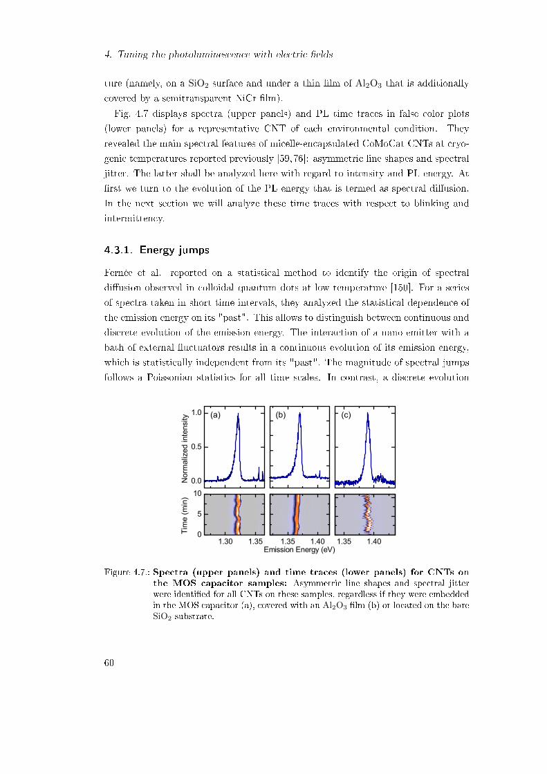
4. Tuning the photoluminescence with electric elds
ture (namely, on a SiO2 surface and under a thin lm of Al2O3 that is additionally
covered by a semitransparent NiCr lm).
Fig. 4.7 displays spectra (upper panels) and PL time traces in false color plots
(lower panels) for a representative CNT of each environmental condition. They
revealed the main spectral features of micelle-encapsulated CoMoCat CNTs at cryo-
genic temperatures reported previously [59,76]: asymmetric line shapes and spectral
jitter. The latter shall be analyzed here with regard to intensity and PL energy. At
rst we turn to the evolution of the PL energy that is termed as spectral diusion.
In the next section we will analyze these time traces with respect to blinking and
intermittency.
4.3.1. Energy jumps
Fernée et al. reported on a statistical method to identify the origin of spectral
diusion observed in colloidal quantum dots at low temperature [150]. For a series
of spectra taken in short time intervals, they analyzed the statistical dependence of
the emission energy on its "past". This allows to distinguish between continuous and
discrete evolution of the emission energy. The interaction of a nano-emitter with a
bath of external uctuators results in a continuous evolution of its emission energy,
which is statistically independent from its "past". The magnitude of spectral jumps
follows a Poissonian statistics for all time scales. In contrast, a discrete evolution
(a) (b) (c)
0.0
0.5
1.0
Nor
mal
ized
inte
nsity
1.30 1.350
5
10
Tim
e (m
in)
1.35 1.40
Emission Energy (eV)1.35 1.40
Figure 4.7.: Spectra (upper panels) and time traces (lower panels) for CNTs onthe MOS capacitor samples: Asymmetric line shapes and spectral jitterwere identied for all CNTs on these samples, regardless if they were embeddedin the MOS capacitor (a), covered with an Al2O3 lm (b) or located on the bareSiO2 substrate.
60

4.3. Jitter analysis
1 10 1000.50
0.52
0.54
0.56
Jump separation, l0.0 0.5 1.0 1.5 2.0
0
1
2
3
4
5
Cor
rela
tion,
C (1
0-2)
Bin width Δ (meV)
0
2
4
6
C/σ
0.0 0.5 1.00
100
200
|νj| (meV)
Occ
uren
ce
σ
C
P(|n
j| ≤Δ
||n j
+l| ≤
Δ)
(a) (b)
Figure 4.8.: Jitter correlation in PL time traces: (a) Conditional probabilityp|νj |≤∆ | |νj+l|≤∆ as a function of the jump separation for a jump separationof ∆ = 0.41 meV. The inset depicts the distribution of spectral jumps |νj |. (b)Correlation C (normalized to the standard deviation σ) as a function of the jumpseparation.
memorizes its recent past and thus is statistically dependent on its former state. This
discrete evolution results from interaction with only few neighboring uctuators.
We analyzed a large number of spectra (N=300-1800) taken sequentially with a
short integration time of 1 s and used a standard tting procedure to obtain the
central PL energy for every spectrum. The magnitude of a spectral jump νj is
dened as the energy dierence EjPL − Ej+1PL taken from two consecutive spectra j
and j+1. To evaluate the statistical dependence of the spectral jumps, we considered
the conditional probability p(l,∆) = p|νj |≤∆ | |νj+l|≤∆, which is the probability to nd
two jumps separated by l−1 (jumps) being both smaller than the bin width ∆. This
probability would be independent from the separation length l, if the magnitude of
the jump νj followed Poissonian statistics without remembering its "past".
However, νj did not exhibit Poissonian statistics for the investigated CNTs, as
exemplied in Fig. 4.8(a). Rather p(l,∆) exceeded systematically the general mean
probability −p(inf,∆) by several standard deviations σ (for the shown example by
7σ). This systematic deviation from a Poissonian statistics becomes further apparent,
if we consider the degree of correlation as a function of the bin width ∆, which is
dened as
C = p(1,∆)− p(inf,∆) . (4.13)
For the CNT discussed here, Fig. 4.8(b) depicts the degree of correlation (normalized
to σ) as a function of the bin width ∆. For all investigated CNTs, C/σ increased
61

4. Tuning the photoluminescence with electric elds
linearly for small ∆ and saturated after C reached its maximum. Since only a limited
number of spectra was considered, C converged to 0 for very large bin width ∆. In
simple terms, more and more energy jumps t in an increasing bin width ∆ and
p(ν,∆) converges to 1. If we consider C/σ, this is compensated as σ decreases
accordingly.
We identied analogous correlation of the spectral jitter for all investigated CNTs
regardless of their environment (Fig. 4.8). In general Cmax > 2.2 σ for all CNTs.
This deviates systematically from a Poissonian statistics and a continuous evolution
of the PL energy, as it would be expected for excitons that diuse freely along a
CNT and probe an averaged bath of close uctuators. Thus, this discrete evolution
can be interpreted by the formation of CNT quantum dots, which interact with
only few neighboring uctuators. Further experimental support for the localization
of excitons in CoMoCat CNT is presented in this thesis: characteristic asymmetric
line-shapes (Chap. 3) and photon anti-bunching (Chap. 5). Chap. 3.5.
In brief, a probabilistic analysis of the spectral jitter of cryogenic, individual CNTs
revealed that the PL energy is statistically dependent on its recent past. As this
characteristic was apparent for all investigated CoMoCat CNTs regardless of their
surrounding (see Fig. 4.9(d-f)), we can exclude detrimental eects on the spectral
diusion of individual CNTs, when they are embedded in a MOS capacitor device.
4.3.2. Intermittency and blinking
The uorescence rate of nano-emitters, may they be nanocrystals or single molecules,
features intermittency or blinking. This has been intensively investigated for many
dierent emitters and was summarized in a detailed review by Cichos et al. [151].
Also for CoMoCat CNTs we were able to identify PL blinking, which followed a
general power-law. Such a power-law was accordingly reported for many colloidal
quantum dots or other single molecule emitters [152].
p(τi) ∝ τ−χii . (4.14)
Here, p(τi) denotes the probability that an emitter remains in the "on" ("o") state
for a period τon (τoff). This law was reported to describe intermittency over 2 to 3
decades of τi with χi ∼ 1.5 [151]. Latest experimental reports [63] show that such
power laws hold also for fast intermittency in the PL of individual CNTs. Although
we were unable to resolve fast intermittency due to a low uorescence rate, we
nd a similar power law holds for the range between 1 and 10 s. Figs. 4.9(a-c)
62

4.3. Jitter analysis
(a) (b) (c)
(d) (e) (f)
1 10
0.01
0.1
1
1 10
0.01
0.1
1
1 10
0.01
0.1
1SiOxAlOx
P(τ on
)
τon (s)
NiCr
τon (s) τon (s)
1 10
0.48
0.51
0.54
Jump separation, l
P(|ν
j| ≤ Δ
| |ν
j+1| ≤
Δ)
1 10
0.51
0.54
0.57
Jump separation, l1 10
0.18
0.21
Jump separation, l
Figure 4.9.: Intermittency and spectral drifting: (a-c) Probability distribution forcharacteristic time in "on" state τon following a power-law (grey solid lines)for each investigated CNT. (d-f) Jitter correlation: Conditional probabilityp|νj |≤∆ | |νj+l|≤∆ as a function of the jump separation. The respective rangeof the standard deviation ±σ is shaded in light blue.
illustrate p(τon) for a representative of each sample regions. For a given time trace,
we investigated the PL intensity for every single spectrum and associated those
showing an intensity above (below) the mean PL intensity with the "on" ("o")
state. Then we summed over the respective number of consecutive spectra in the
"on" ("o") state. Generally χon was reported between 1.1 and 2.2 for various nano-
emitters [151], which agrees with our ndings of χon ranging from 1.08 to 1.52 and a
mean of value of 1.28± 0.16. We identied an analogous power-law for p(τoff) with
χoff ranging between 0.97 and 1.63.
In the context of molecules or nanocrystals such intermittency behavior was gen-
erally assigned to (photo activated) charging. Whereas χon is generally independent
of the dielectric surrounding [151], colloidal quantum dots show a systematic relation
between χoff and ε due to random charging and de-charging [153]. However, we could
not identify a positive relation between the dielectric medium around a CNT and
χoff .
PL intermittency of individual CNTs could originate from charging and discharg-
ing of CNTs. Such charging would shelve the exciton to a trion state [4749] while
quenching the PL intensity in favor of a trion satellite peak outside the detection
63

4. Tuning the photoluminescence with electric elds
1.25 1.30 1.35 1.400.0
0.5
1.0
Nor
mal
ized
PL
inte
nsity
PL energy (eV)1.25 1.30 1.35 1.40
PL energy (eV)1.25 1.30 1.35 1.40
PL energy (eV)
ΔK
+ħωph
ΔSTΔST
X X X(a) (b) (c)
XT
XTXKType A Type B
Figure 4.10.: Example spectra for type A and type B CNTs: (a) Spectrum of atype A CNT characterized by a single emission line of the bright exciton X.(b-c) Spectra of type B CNTs showing multiple emission lines due to brighten-ing of k-momentum exciton XK and triplet excitons XT. The respective energysplittings ∆i are dened as positive values.
range. As we will show in the last section of this chapter, this doping of CNTs gov-
erned by the nearest surrounding of a CNT quantum dot. This close surrounding
consists not only on the dielectric medium (SiO2 and Al2O3) but also on an exper-
imentally uncontrolled amount of surfactant molecules. In consequence, the closer
dielectric medium around a CNT could vary between ε ≈ 2.2 for a CNT packed into
sc surfactant and ε > 3.9 for a CNT close to SiO2 and Al2O3. This could also impede
the identication of positive relation between an locally varying ε and χoff .
In conclusion, the general intermittency of the PL rate from individual CNTs was
not aected by embedding these into a MOS capacitor device. Since such blinking is
generally associated with charge trapping [151] or the mobility of quenching sites [63],
it is consistent with the picture of exciton localization at cryogenic temperature.
4.4. Classication of CNTs
4.4.1. Multiple peak emission spectra
Before we analyze the PL of individual CNTs as a function of an externally applied
electric eld, we turn back to the spectral properties of CoMoCat CNTs. In addition
to one-peak spectra, which we discussed in Chap. 3, we have identied a second type
of spectral emission prole from individual CNTs. The PL spectra of these CNTs
showed multiple emission peaks. Two exemplary spectra are depicted in Fig. 4.10. In
most cases, we found a bright asymmetric emission peak and a less intense satellite
peak shifted to the red. However, in some cases the satellite peaks were on the blue
side.
64

4.4. Classication of CNTs
(a)
-50 0 50 100 150 2000
1
2
3
4
Energy splitting (meV)
ΔST
ΔD
ε = 4.6Δ
ph= 160 meV
0
4
8
Type B
Occ
urre
nce
Type B
0
4
8
Theory
|Δi|
Δi
(c)ΔK + Δph
(b)
Figure 4.11.: Energy splittings in two-peaked emission spectra: (a) Investigating29 type B CNTs, the energy splitting ∆i between bright emission line andthe satellite peak accumulated around -50 meV, +50 meV and 120 meV. (b)Statistical distribution of |∆i|. (c) Theoretically expected energy splittings ofdark exciton (singlet) states from the bright exciton for chiralities within ourspectral range. The values base on calculations summarized in Fig. 2.8.
Statistics of the energy splittings ∆i between the bright emission line and satellite
peak are illustrated in Fig. 4.11. We identied them clustering around 120 meV and
±50 meV, respectively. This accumulation around two discrete energies speaks in
favor of a CNT intrinsic energy scale, rather than an external scale like the previously
identied depth of localization potentials (see Chap. 3.5).
Indeed, these splittings agree with theoretical predictions of the singlet-triplet
splitting [55] and the energy of the k-momentum excitons [34]. Here, we took account
for the CNT environment by screening accordingly the Coulomb interaction using
Eq. (2.22). We found the best agreement assuming an average dielectric constant
of ε = 4.6, which is expected for CNTs in a medium consisting of aluminium oxide
(εAl2O3 = 9.1), silicon oxide (εSiO2 = 3.9) and sodium-cholate (εsc ' 3.5). Fig. 4.11(c)
shows theoretical energy splittings for CNT chiralities within our spectral range. We
assign satellites that are red-shifted by ∼ 50 meV from the bright exciton as emission
from the triplet exciton XT . In the same way, we assigned splittings of −50 meV to
a less intense bright exciton line and an intense triplet exciton line. Furthermore,
satellites with an energy splitting of ∼ 120 meV were presumably phonon-sidebands
of the k-momentum exciton.
We did not detect any signatures of brightening the lowest dark (singlet) exciton
65

4. Tuning the photoluminescence with electric elds
state (XD). Nevertheless, emission from the dark exciton was experimentally realized
only by use of axial magnetic elds [3941] and bases on magnetic ux induced valley
mixing of bright and dark exciton states [110]. However, theoretical calculations show
that such valley mixing cannot originate from impurities [154].
The occurrence of satellite peaks in the emission spectra of individual CNTs is
in agreement with recent reports on brightening emission from the k-momentum
(singlet) exciton [42,43] or from triplet exciton states [4446,112]. Whereas the rst
results from mixing of the bright exciton with the k-momentum excitons via exciton-
phonon coupling, the other is a consequence of impurity induced spin-orbit coupling.
A proposed mechanism is based on a single impurity that distorts the orbitals of
single carbon atoms from sp2 to sp3 and results in enhanced spin-orbit coupling [78].
Hence, bright (=singlet) and dark (=triplet) exciton states are admixed so that even
the dark triplet state acquires a nite oscillator strength [79]. In most reports, the
impurities were actively added to the CNTs, for instance by chemical adsorption of
hydrogen atoms [112]. Also CNTs treated by intense laser radiation showed satellite
emission peaks from exciton triplet states [43,155].
Within our experiments the used CoMoCat CNTs were commercially purchased
in solution. However, dissolving and individualizing CNTs in an aqueous solution re-
quired harsh treatment like ultra-sonication that creates lattice defects [156]. Hence,
a certain degree of lattice defects was expected. Our results suggest that a large frac-
tion of CNTs was unable to preserve the symmetry upon the cool-down to cryogenic
temperatures. Structural defects or charge traps in the surrounding dielectrics were
presumably responsible for the breakdown of the trigonal warping model used to
describe optical transitions in ideal CNTs. At this point, however, our experiments
did not provide insight into the detailed microscopic origin of the reconguration of
excitonic states in CNTs at cryogenic temperatures.
However, we observed similar two-peaked spectra also for a dierent CNT material
of substrate supported CVD CNTs that we will discuss in Chap. 5. These CNTs
featured a single emission peak, when the spectra were recorded within 1 s. However,
accumulating their spectral diusion resulted in two-peaked emission proles with
similar energy splittings of ±50 meV. Although this agrees with the splitting to the
triplet exciton, the discrete switching between emission either from the singlet or
from the triplet state, contrast the picture of state mixing giving nite oscillator
strength to both exciton states.
66

4.5. Electric eld sweeps
4.4.2. Emission spectra of type A and type B CNTs
Based on the previous considerations we categorized CNTs into two major classes:
Type A CNTs were characterized by a single asymmetric emission line due to re-
combination from the bright exciton X. In contrast, type B CNTs showed additional
emission from dark exciton states, namely triplet excitons XT or phonon-sidebands
XK. Hence, these were identied by their emission spectra showing multiple emission
peaks.
A similar categorization was introduced by Matsuda et al. [134] for investigation
of spectra diusion. Whereas type A showed single emission lines with only small
spectral diusion, CNTs with a presumably broken symmetry showed an increased
spectral diusion, which was considered in the framework of a quantum-conned
Stark eect.
As we will show in the following, Matsuda's categorization agrees with our nd-
ings. Localized excitons in CNTs with a broken symmetry carry a permanent dipole
moment that couples the PL energy eciently to electric eld, like external charge
uctuations. Hence, type B CNTs show a broader line-width and an increased spec-
tral diusion. In contrast, CNTs of type A preserve their symmetry even at low
temperature and do not exhibit a permanent dipole moment. As consequence their
PL is robust against surrounding charge uctuations. Thus, type A CNTs show a
narrow line-width with a stable emission energy.
4.5. Electric eld sweeps
For all investigated MOS devices, the overall capacitance changed only on the order of
a few percent as a function of the applied gate voltage Vg as we have shown previously
in Chap. 4.2. This allowed to treat the homogeneous electric eld strength F simply
as a linear function of the gate voltage, F = Vg/(d1 + d2). However, we limited
the gate voltage to V maxg = 16 − 30 V to keep the samples from fatal breakdowns.
Depending on the thickness d2 of the aluminium oxide layer electric elds up to
±0.3 V/nm were generated.
In the following, we recorded PL spectra of individual CNTs as a function of the
electric eld F . In order to distinguish the resulting eects on the PL from the
omnipresent spectral diusion and to trace possible hysteresis eects, we used the
following voltage sweep scheme. At rst, we took 10-15 PL spectra while keeping
top and back gates grounded (Vg = 0). Then we ramped the electric eld to its
maximum Fmax in discrete steps ∆Vg (0.5 − 2.5 V) while recording a spectrum
67

4. Tuning the photoluminescence with electric elds
-20020
-0.20.00.2
F (GV/
m)
PL e
nerg
y (e
V)
Vg (V
)
1.30
1.32
1.34
0.00.51.0
I/Imax
0.5 1.0
Normalized PL intensity
(a)
(b)
(c)
(d)
time
Figure 4.12.: Polarizability and reversible PL quenching: (a) Electric eld sweep. (b)Contour plot of the PL of an individual CNT showing only small shifts of the PLenergy but pronounced reversible quenching of the PL intensity for negativeelectric elds. (c) Fitted PL intensity illustrating reversible quenching. (d)Spectrum at Vg = 0.
after each step. From Fmax we ramped the eld in the same way to its minimum
Fmin ≈ −Fmin(V maxg = V min
g ) and nally back to zero. In a nutshell, we recorded a
short time trace with no applied electric eld and two spectra for every electric eld
step. The smoothed trace of such an electric eld sweep is depicted in Fig. 4.14(a).
During these sweeps, we kept all other controllable parameters constant (sample
position, excitation power, wavelength and polarization). For each CNT investigated
the excitation wavelength was respectively tuned to a resonance 50-175 meV above
EPL to increase the PL emission intensity. To maximize the PL emission, the axis
of linear polarization was adjusted parallel to the tube axis.
4.5.1. Transverse polarizability of excitons
Following this experimental scheme, we investigated type A CNTs, which we pre-
classied due to their single asymmetric emission line. Fig. 4.12 exemplies the
trace of the PL spectrum as a function of the electric eld. For all type A CNTs
investigated the PL energy EPL varied slightly with the electric eld. However, some
type A CNTs - as the one depicted here - exhibited a reversible quenching of the PL
intensity to less than 10 % of its initial intensity. We could associate this quenching
either to doping of the CNT or to detuning of exciton localization potential from the
excitation laser. Both eects will be discussed in the second part of this chapter.
Here, we focus on the energy dispersion of the PL as a function of the electric
68

4.5. Electric eld sweeps
(a) (b)Type A
-30 -15 0 15 30
1.31
1.32
1.33
β = (- 45 ± 13) meV GV-2m-2
Vg (V)
PL e
nerg
y (e
V)F0= -1.4 V
1.30 1.35 1.40
-300
-150
0
PL energy (eV)
β (m
eVnm
2 V-2)
Figure 4.13.: Transverse polarizability of CNTs: (a) PL energy as a function of theapplied eld. Orange solid line displays a quadratic t with the parametersβ and F0 representing the transverse polarizability and the local eld mod-ulation, respectively. (b) Statistics on the polarizability: β as a function ofEPL. CNTs, which exhibited a high local eld modulation (|F0| > 8 V ) areindicated by lled circles, where as open circles represent CNTs with smalllocal eld modulations (|F0| < 8 V ). The grey solid line depicts the average ofβ = −40± 20 meV/(V/nm)2.
eld strength. Fig. 4.13(a) illustrates the energy of the PL maximum as a function
of the gate voltage (for the same CNT shown in Fig. 4.12). For all type A CNTs
we observed a quadratic relation between the applied electric eld and the emission
energy.
Previous reports considered energy shifts in the PL of individual CNTs as a result
of mechanical stress [132]. However, energy shifts observed within our experiments
were a factor of 100 bigger than those expected by the electrostatic pressure between
the biased gates12. Thus, we exclude that the PL shifts were of mechanical origin.
Rather, we argue that applied electric eld probes for the transversal polarizability
12CNTs embedded in a frozen water ambient show an energy shift due to external longitudinalstress [132]. Depending on their chirality the shift is either to the red or the blue with up to12 meV/GPa. In contrast, the electrostatic pressure between the biased top and back gate actedonly perpendicular to the CNT axes. We consider the work W to charge the capacitance inorder to estimate the electrostatic pressure within our device.
W =1
2CV 2
g =1
2εε0
A
dV 2g . (4.15)
With the force f = W/d, the pressure p is given by
p =f
A=
1
2εε0
V 2g
d2. (4.16)
and does not exceed 3.7 MPa for a maximum voltage V maxg = 30 V and a minimal capacitor
distance (d1 + d2)min = 107 nm. But even if we assume a similar energy shift due to perpendic-ular pressure as reported for longitudinal stress, this energy shift would not exceed a few tensµeV(' 42 meV/GPa · 3.7 MPa). This is by about a factor 100 smaller than the here consideredshifts of 3.2 meV (β · F 2 ' −40 meV(GV/m)2 · (30 V/107 nm)2).
69

4. Tuning the photoluminescence with electric elds
of excitons. For type A CNTs the shift of the PL energy was best approximated by
a parabolic function E(F ) = EPL + β(F − F0)2 where EPL is the PL energy at
Vg = 0, and F0 = V0/(d1 + d2) accounts for local eld modications, e.g. due to the
presence of a charge in the vicinity of the CNT. The tting procedure yields local
built-in elds of the order of ±0.1 V/nm. This value is as big as the strength of the
externally applied eld and is consistent with the electric eld strength of a single
elementary charge impurity located as close as ∼ 2 nm to the CNT. This distance
agrees well with rough estimations of the charge state density we evaluated from
CV measurements. In this context, a random distribution of oxide charges in the
dielectric medium would account for one charge state in a radius of 2.4 nm around
a 200 nm CNT (see Chap. 4.2.3).
A summary of the t parameter β is depicted in Fig. 4.13(b). Most type A
CNTs exhibited eld-induced redshifts with an average curvature of β = −40 ±20 meV/(V/nm)2. However, we also identied insignicant shifts for three CNTs,
which featured a high value of |F0|. For those, the here generated homogeneous elec-
tric elds were insucient to outperform local eld modulations. Assuming that the
energy dispersion of type A CNTs is entirely due to the the quantum conned Stark
eect, we interpret β as the transverse exciton polarizability. This is consistent with
recent experimental [135] and theoretical [82] results for CNT excitons in perpendic-
ular electric eld as well as calculations of the transverse CNT polarizability based
on tight-binding models [157159] or rst-principle approaches [160162].
However, it should be taken into account that a blueshift due to eld-induced dop-
ing [163] would counteract a redshift caused by the exciton polarizability whenever
doping occurs. We could not identify such a blueshift for those CNTs that showed
signatures consistent with the doping of excitons (discussed in Chap. 4.6).
4.5.2. Permanent dipole moments
The energy dispersion changes drastically if we turn to type B CNTs as exemplied
in Fig. 4.14. Their two-peaked spectra featured wide shifts of the emission energy
of the bright exciton X and the satellite XT as a function of the electric eld F .
Depending on the polarity of F , the PL energy was shifted to both the red and the
blue exceeding for some CNTs ±10 meV or several line widths.
Furthermore, the PL intensity was quenched as a function of the electric eld
F , which is illustrated in Fig. 4.14(c). Since this quenching was reversible on both
emission peaks, we interpret this with PL energy shifts inducing misalignment of the
excitation resonances with the excitation laser.
70

4.5. Electric eld sweeps
-0.20.00.2
-23023
F (GV/
m)
PL e
nerg
y (e
V)
Vg (V
)
1.38
1.40
1.34
1.36 x10
x10
0.5
1.0
I/Imax
0|1
0.0
0.5
0.0 0.5 1.0Normalized PL intensity
(a)
(b)
(c)
(d)
time
X
XT
Figure 4.14.: Permanent dipole moment of an individual CNT - part I: (a) Electriceld sweep. (b) Contour plot of the PL of an individual type B CNT showingdistinctly eld induced shifts on the bright exciton X and the triplet XT. (c)Fitted PL intensity illustrating reversible quenching due to loss of resonancewith the excitation laser (d) Spectrum at Vg = 20 V.
Plotting the energy of the PL maxima as a function of Vg (Fig. 4.15(a)) re-
vealed a linear energy shift and a negligible parabolic component, which we t with
E(F ) = EPL + pF . The presence of a transverse permanent dipole moment p, which
gives rise to a linear Stark shift, is at rst surprising since the C2 rotational symmetry
(see Chap. 2.1.2) forbids pristine CNTs to carry such a permanent dipole moment.
Ab-initio calculations state a band-gap re-normalization for zig-zag and chiral
CNTs with mono-vacancy defects [164,165]. Their band-gap is predicted to be mod-
ied linearly with the strength of a perpendicularly applied electric eld. Sign and
magnitude of the resulting energy shifts depend strongly on the orientation of the
electric eld to the remaining symmetry axis of the defective CNT. For (anti-)parallel
orientation maximum energy shifts of |∆E/∆F | ' 0.63 eÅ are expected where we
scaled the reported theoretical values to the here considered CNT diameters. As
depicted in Fig. 4.15 this agrees with our ndings.
Despite this coincidence in ∆E/∆F , this scenario is not applicable to the CNTs
of our samples since it also implies a defect-induced band-gap reduction of the order
of 50% at zero external eld. Moreover, a general re-normalization of the band
gap contradicts our ndings of opposing energy shifts for the bright exciton and its
71

4. Tuning the photoluminescence with electric elds
1.30 1.35 1.40-1.0
0.0
1.0
PL e
nerg
y (e
V)PL energy (eV)
p (e
x Å)
1.38
1.39
1.40
1.41
-20 -10 0 10 20
1.33
1.34
1.35
Vg (V)
0.0 0.5 1.00
2
4
6
8
Occ
urre
nce
|p| (e x Å)
(a) (b)
(c)
ΔST
Type B
Figure 4.15.: Permanent dipole moment of an individual CNT - part II: (a) Energyof the PL maximum of the bright exciton peak X (lled circles) and tripletexciton peak XT (open circles) as a function of the applied gate voltage. Thepermanent dipole moment equals the slope of the linear ts (solid blue lines)(b) Permanent dipole moment as a function of PL energy. (c) The histogramdisplays the distribution of the permanent dipole moment.
satellite in almost all type B CNTs, which is exemplied in Fig. 4.16(b). Instead of
a band-gap re-normalization, we argue that defect-induced admixing of bright and
dark excitons may give rise to built-in dipole moments that are a small fraction of the
exciton Bohr radius p ' 0.01·aB·e. Indeed, built-in dipole moments were only present
in type B CNTs, which were characterized by their state mixing between bright and
dark exciton states. As we illustrated in Fig. 4.11 their two-peaked spectra could be
interpreted as arising from admixing of triplet excitons to the bright exciton state.
Their opposing energy shifts can be interpreted as the anti-parallel alignment
of the permanent dipole moments of singlet pX and triplet exciton pXT . Further
indication for a fundamental physical origin is illustrated in Fig. 4.16(a), which plots
the magnitude of the observed singlet dipole moment pX as a function of the degree of
state mixing. This degree was quantied by the intensity ratio between the XT and
X emission peaks13. Since the magnitude of the dipole moment correlates with the
degree of state mixing, both could be induced by defects, which give rise to spin-orbit
coupling [78] and permanent dipole moments of excitons. Within our experiments
13Due to a not resolved mechanism some CNTs exhibited an intense emission from the XT stateand only faint emission from X. For simplicity we consider the inverse intensity ratio betweenXT and X for those CNTs.
72

4.5. Electric eld sweeps
-1.0 -0.5 0.0 0.5 1.0-1.0
-0.5
0.0
0.5
1.0
p XT (
e Å
)
pX (e Å)
0.0 0.1 0.20.0
0.5
1.0
|pX| (
e Å
)
Intensity ratio
(a) (b)
Figure 4.16.: State mixing and permanent dipole moment: (a) Magnitude of thepermanent dipole moment |pX | of the bright exciton state as a function of thedegree of state mixing here quantied by the intensity ratio of X and XT.(b) Permanent dipole moments of the triplet exciton state pXT and the brightexcitons pXT are of opposite signs.
only one single CNTs disagrees with the above considered mechanism. Its dipole
moments are depicted as open circles in Fig. 4.16.
However, the dipole moments observed here exhibit a transversal component,
which cannot arise from mixing of exciton states from the E11 manifold. Rather,
admixing to the E12 (or E21) manifold is required. Theoretical calculations show,
that the energy bands even of pristine CNTs should recongure in transversal electric
elds, although the band-gap is unaected F < 0.3 V/nm [166]. This is consistent
with our ndings of an only slightly varied PL energy of type A CNTs. Though a
reconguration of the energy bands could admix singlet and triplet excitons from
the E11 manifold to the E12 (or E21) manifold. In consequence, singlet and triplet
excitons would acquire a permanent transversal dipole moment as they exhibited in
a linear energy shift as a function of the transversal electric eld.
In conclusion, we have identied CNTs with a broken symmetry featuring two-
peaked PL emission proles that arise from mixing dark and bright excitons states.
By their energy splitting we could assign satellite peaks to the triplet exciton XT or
the phonon sideband of the k-momentum exciton XK, respectively. In a transver-
sal electric eld, we observed linear, but opposing shifts on PL energy of bright
and satellite PL emission, which we interpret with anti-parallel permanent dipole
moments of both states. As states from the E11 exciton manifold do not intrinsi-
cally feature transversal dipole elements, the permanent dipole moments observed
here could presumably arise from admixing of the E11 to the E12 (or E21) exciton
manifold. However, a comprehensive understanding requires further theoretical and
73

4. Tuning the photoluminescence with electric elds
experimental investigation. Nevertheless, due to the permanent dipole moment of
CNTs with a broken symmetry - here termed as type B CNTs - their PL energy
couples eciently to external charge uctuations. This broadens the line width of
the PL emission prole (see Fig. 4.10) and increases spectral diusion, which was
reported in Ref. [134]
4.6. Emission from trion states
In conclusion of this chapter we focus on CNTs with a single emission line (type A).
As we have shown previously, their PL energy varied only slightly with the applied
electric eld. However, some type A CNTs exhibited severe but reversible quenching
of the PL intensity, which cannot be explained solely due to an o-resonant excita-
tion. In addition, some type A CNTs featured the emergence of a satellite peak as
a function of the applied eld. As the energy splitting of the satellite to the bright
excitons agrees with the trion energy splitting ∆±, it seems likely that this satellite
originates from electric eld mediated creation of trions in CNTs. In the last part of
this chapter, we focus on a second quenching mechanism, which is presumably due
to the variation of the trapping potential for localized excitons.
It appears that both characteristics could be attributed to charge states that were
switchable by the external gate voltage and could dominate the photo-physics of
individual CNTs. Within the MOS capacitor, these charge impurities were located
in both the insulating oxide lms (termed as QOT) and on the oxide-semiconductor
interface (termed as QIT) and were apparent in the CV characteristic of the devices
(see Chap. 4.2). However, charge impurities at the oxide-semiconductor interface
were with 100 nm too far away from the CNTs to create a considerable eld strength
and inhomogeneity. In contrast, oxide charge states were located in close neighbor-
hood to the CNTs. As we have stated before, we expect on average one charge state
in a radius of 2.4 nm around a 200 nm CNT.
We begin with CNTs that showed the emergence of a satellite peak as a function
of the applied gate voltage. Fig. 4.17(a) illustrates exemplarily a PL spectrum at
Vg = 0 . This consisted of a single asymmetric line X at ∼ 1.36 eV indicating emission
from the bright exciton of an individual (6,4) CNT (comparison with [88]). When
we ramped the gate voltage up to a positive voltage of Vg = 16 V, the PL from the
bright exciton was steadily quenched. The quenching of the bright exciton emission
was accompanied by the emergence of a satellite peak X± split by ∆± ' 100 meV
from the main PL resonance. In any case, the creation of this satellite peak was
74

4.6. Emission from trion states
robust and reversible. It came along with a quenching of the PL emission from the
bright exciton.
The upper panel of Fig. 4.17(b) depicts the intensity of both emission peaks IX and
IX± as a function of the applied gate voltage14. As a typical feature for CNTs on
substrate both emission lines showed pronounced intensity uctuations. However,14Only for this example, IX was quenched also for negative voltages. This might originate from
a delocalization process as discussed in the previous chapter. However, the occurrence of bothquenching mechanisms was more a rare exceptional case and not reproduced by any other CNT.
(a)
(b)
0.0
0.5
1.0
I/Im
ax
x 30
1.25 1.30 1.350.01
0.1
1
X±
X16V
Nor
mal
ized
inte
nsity
PL energy (eV)
0V
-200
20
V g (V)
time
0
1
I/Im
ax
-15 0 15
1
10
I X±/I
X (1
0-2)
Gate voltage (V)
0
1
I X±/I
X (1
0-2)
(c)
Figure 4.17.: Voltage-induced trion generation in a single carbon nanotube: Thetrion satellite X± emerged for positive gate voltages redshifted by 100 meVwith respect to the main emission peak at 1.36 eV (blue and orange spectrain (a) were recorded at 0 V and +16 V, respectively; the insets show zoomsto individual spectra in the satellite peak region for given gate voltages). (b)Upper panel: The integrated PL intensity of the main peak IX (grey datapoints) decreased for positive gate voltages whereas the intensity of the red-shifted satellite IX± (purple data points, multiplied by a factor of 30) increasesfor positive and vanishes for negative voltages. Lower panel: The intensity ratioIX±/IX on a log scale as a function of the gate voltage. As IX±/IX featureda smoother trace, X and X± were aected by the same intensity uctuations.The orange solid line displays an exponential t for Vg ≥ −2.5. (c) Theemission intensity was reversibly switched between minimum and maximumvalues when we applied a square wave voltage between -20 V and +20 V (greyand purple solid lines correspond to the peak intensity of the main resonanceand the satellite, respectively). Data in (a-b) and (c) were measured on twodierent CNTs.
75

4. Tuning the photoluminescence with electric elds
the ratio between both intensities IX±/IX was less aected by these uctuations,
which indicates that both emission lines originated from the same CNT (lower panel
in Fig. 4.17(b)).
Furthermore, we were able to perform a robust digital switching scheme between
X and X±, which is illustrated in Fig. 4.17(c) for a second CNT. We employed a
square wave voltage scheme switching Vg between +20 V and −20 V (upper panel).
Once again, the intensity ratio IX±/IX followed the squares of the applied voltage.
Similar red-shifted satellites have been observed in recent experiments and at-
tributed either to a band-gap re-normalization due to an oxygen substitute [48, 51]
or to the formation of charged exciton complexes (trions) [47,49,50]. All reports in-
cluded furthermore a quenching of the bright exciton intensity when these satellites
emerged. As we will discuss now, the energy splitting between X and X± agrees with
these experimental reports and theoretical calculations [55,81]. Thus, the emergence
of X± could originate from of CNT with an additional charge ±e. This gives rise
to the formation of trions while the X intensity is quenched in favor of PL emission
from the trion peak X±.
Fig. 4.18 summarizes the splitting ∆± of the reversibly created satellite peaks
for type A CNTs and the splittings found on type B CNTs (see Chap. 4.4). In
addition to the splitting to the triplet state ∆ST and the sideband of the k-momentum
exciton ∆K + ~ωph identied previously, ∆± constitutes a third class in the energy
hierarchy of the exciton ne structure. We emphasize that all previous reports on
the optical emission from trion states included particular screening eects. These
were indispensable to bring the respective experimental results [47,49] in agreement
with the theoretical values for the trion binding energy predicted by Rønnow et
al. [81]. Theoretical reference values for ∆± were presented in Chap. 2.3.6. However,
newest theoretical considerations [167] predict that the trion binding energy is much
less susceptible to Coulomb screening than anticipated by the general scaling of the
Coulomb energies (Eq. 2.22). Thus, we neglected any screening eect on the trion
binding energy, but re-scaled the fraction of the singlet-triplet exchange interaction
to the environment (ε = 4.6). For all CNTs featuring emission from trion states we
nd energy splittings ∆± that agree with theoretical calculations.
Our ndings add a new paradigm to the generation of trions in CNTs: their
intensity can be controlled with a static electric eld. As depicted in the lower panel
in Fig. 4.17(b), the intensity ratio increased with the gate voltage. Whereas the PL
emission spectra consisted of a single peak for Vg < 2.5 V, the generation of trions set
76

4.6. Emission from trion states
-50 0 50 100 150 20001234
ΔDO
ccur
renc
e
Energy splitting (meV)
Δ
ST
ε = 4.6Δ
ph= 160meV
ΔK + Δ
ph
Δ±
0
2
4
6
8
Theory
|Δi|
Type B
Type B
0
2
4
6
8
Type A
Figure 4.18.: Complete hierarchy of low-energetic PL emission: Upper panel: Ex-perimentally conrmed energy splittings to the bright exciton line X for CNTswith broken symmetry (type B in orange) and electrically doped CNTs (typeA in dark blue). Lower panel: Considering only chiralities wit EPL withinthe investigated spectral range, the histogram depicts theoretically predictedenergy splitting to the bright exciton of the lowest dark exciton XD, tripletexciton XT, trion X± and the phonon-sideband of the k-momentum excitonXK + ∆ph.
in after this threshold and increased exponentially15. A simple exponential function,
which is illustrated as a solid line, reproduces the variation of the intensity ratio
IX±/IX ∝ exp(Vg/6.1 V) with the applied gate voltage for Vg ≥ 0. This could rather
originate from the CNT charging process than being a feature of the trion state
itself. In previous reports CNTs were either doped all optically [49] or by chemical
adsorption of complex add-molecules [47]. Within our experiments trion states were
presumably generated by tunneling of charges from a close source onto the CNTs.
Oxide charge states or other impurities of the insulator could be possible sources. By
varying the gate voltage, we would lower the tunnel barrier, which gives exponential
rise of doping. This exponential increase agrees with the fundamental theoretical
considerations of the WKB approximation for tunneling in quantum mechanics [168].
In summary, we have identied PL emission from all excitonic states of today's
known ne structure - excepting the lowest dark exciton singlet state. Symmetry
breaking mixes dark and bright exciton states and allows dipole-forbidden transi-
tions, which brightens the exciton triplet XT . Furthermore, we observed emission
due to k-momentum states XK in their phonon sidebands at ∆K + ~ωph. Last but
not least, we identied the generation of charged exciton complexes (trions) and their
15We also observed the emergence of trion peak with negative voltages. The polarity of triongeneration can be understood in the arrangement of the charge impurity to the CNT. The osetof a few volts agrees with the built in elds of our devices, see Fig. 4.6.
77

4. Tuning the photoluminescence with electric elds
emission lines X±. These were induced via the applied electric eld via tunneling
of charges from a close oxide charge state. However, the small number of doped
CNTs registered in our experiments indicate that such charge sources were rare in
our devices. In future experiments devices with a reduced silicon oxide thickness
would feature a dened tunnel barrier to the back gate. This could allow for tailored
doping of individual CNTs.
4.7. Tuning the localization potentials of excitons
4.7.1. Photoluminescence excitation spectroscopy
Photoluminescence excitation (PLE) spectroscopy is a powerful experimental tech-
nique that monitors the emission of a semiconducting material as a function of the
excitation wavelength [136]. In the past, this technique was successfully employed
on CNTs revealing many of their fundamental properties. It resolved the chirality
distribution of a CNT ensemble by the ratio of the E11 emission resonance to the
E22 excitation resonance [88]. Also the excitonic nature of photoluminescence was
rstly revealed by PLE spectroscopy of individual CNTs [37]. However, at low tem-
perature the excitation spectrum of an individual CNT is not solely determined by
the electronic E22 resonance. Rather electron-phonon coupling establishes phonon-
sidebands between the energy of the bright exciton (' E11) and E22 [8387]. Ac-
tually, phonon-assisted excitation has been identied as ecient as excitation via
electronic E22 states [83]. Typically, these sidebands occur at the major phonon
modes of a CNT, which are namely the radial breathing mode (RBM), the graphene
modes (G±) and the disorder mode (D). This last mode arises from vibration of
non-hexagonal carbon rings including many lattice defects like vacancies, 5-7 defects
and Stone-Walsh defects [169].
We dene the laser detuning δL as the dierence between the excitation laser
energy and the PL emission energy:
δL = Eexc − EPL . (4.17)
For recording of PLE spectra, we excited individual CNTs with a continuous exci-
tation beam - polarized parallel to the CNT axis and operated at constant intensity
' 10 µW/µm2. By systematic variation of the laser wavelength, we shifted the laser
detuning δL in steps of 0.75 meV in a range between 30 to 300 meV and recorded
an emission spectra after every step. We used a standard tting routine that t a
78

4.7. Tuning the localization potentials of excitons
Lorentzian peak to the PL emission spectra and gave a reliable measure of the PL
intensity. A PLE spectrum plots this integrated PL intensity as a function of the
laser detuning δL.
For all investigated CNTs the PLE spectra exhibited pronounced variations of the
integrated PL intensity and featured excitation resonances where the PL intensity
showed a local maximum. For many investigated CNTs the energy detuning at these
maxima coincided with the energy of phonon-modes, e.g. RBM, D, G±. These
ndings agree with an excitation mechanism via phonon-assisted sidebands reported
previously [8387].
However, some CNTs showed resonances at characteristic detunings that disagree
with the phonon spectrum. Fig. 4.19 exemplarily depicts PL and PLE spectrum
of such an individual CNT. This CNT was located on the sample next to the ac-
tual capacitor and was covered only by an aluminium oxide layer. As typical for
a type A CNT, its PL spectrum consisted of a single asymmetric emission line at
EPL = 1.288 meV. Its PLE spectrum featured several broad resonances, which in-
cluded a striking phonon-sideband due to the RBM mode but showed only small
signatures of other common phonon-assisted sidebands (D,G± modes). Especially
1
10
Inte
grat
ed
PL in
tens
ity (a
.u.)
1.26 1.290
1
2
(8,3)
PL in
tens
ity
(cts
s-1 µ
W-1)
PL energy (eV)
0 1 2 3 4 5 60
100
200
δ L (m
eV)
n × Δa 50 100 150 200
0
1
2
3 RBM
IFM-
oTO
IFM+ D G-G+
M-M+
Laser detuning δL (meV)
Diff
eren
ce to
ha
rmon
ic fi
t (a.
u.)
(a) (b)
(c)
(d)
Figure 4.19.: Photoluminescence excitation spectra revealing exciton localization:(a) Spectra of an individual CNT with chirality (9,1) continuously excited at880 nm, which equals a laser detuning δL ' 130 meV. (b) Integrated PL inten-sity as a function of laser detuning δL reveals an excitation spectra dominatedby a harmonic localization potential and phonon-assisted sidebands. The greysolid line depicts a t of six Lorentzian peaks with equal width Γa = 5.8 meV.(c) The central energies of these peaks were equidistant, which indicates a har-monic trapping with a fundamental localization energy ∆a = 37.4 meV. (d)The dierence between t and experimental data coincides with a number ofphonon energies, which are reported [170].
79

4. Tuning the photoluminescence with electric elds
the excitation resonance around 110 meV disagrees with the energy of phonons in
CNTs.
As we will discuss now, such PLE spectra could originate from an alternate excita-
tion mechanism, which occurs in addition to the phonon-sideband assisted excitation
of excitons in cryogenic CNTs. As exemplied by the solid line in Fig. 4.19(b), we
were able to reproduce most of the PLE spectra by tting (here six) Lorentzian
peaks of equal width. Subtracting these Lorentzians from the PLE gave a "reduced
excitation spectrum".
For the here exemplied CNT, this reduced excitation spectrum is depicted in
Fig. 4.19(d) and local maxima could be assigned to phonon sidebands [170]. Most
intense peak at at 40.3 meV was clearly assigned to the RBM mode as this value
agrees with the theoretical prediction of 40.6 meV of a (9,1) CNT [171]. However,
the expected PL energy of a (9,1) CNT [88] disagrees with the here observed EPL =
1.288 eV, which is shifted by ∆E = 54 meV to the red. This energy scale is identical
to the temperature induced energy shifts, which we presented in Chap. 3.
The second dominant phonon sideband was the out-of-plane transverse optical
(oTO) phonon mode. Also its overtones (M±) were visible [172]. The occurrence of
an oTO phonon mode is even more remarkable since the mirror symmetry of graphene
forbids eective optical coupling to this phonon mode [172]. However, coupling to
the oTO mode is associated with out-of-plane discontinuities in graphene [173]. Here,
this discontinuity could be a chemically adsorbed aluminium atom (the CNT was
covered by aluminium oxide). By forming an AlC2 bond, the Al atom would be
located outside the CNT shell [174] giving rise to out-of-plane vibrational modes.
Indeed, the energy of the vibrational rocking mode of AlC2 coincides with the here
observed energy of 105 meV [175].
However, the greater share of the excitation spectrum was not governed by phonon
resonances but dominated by six Lorentzian shaped peaks. At rst glance, the tting
of Lorentzians peaks of equal width may appear as arbitrary. Nevertheless, the
central energies of these peaks could be assigned as the rst to the sixth multiple
of a fundamental energy ∆a = 37.4 meV as illustrated in Fig. 4.19(c). Thus, it can
be interpreted as the six harmonics of an exciton localized in an harmonic trapping
potential. Analogous quantum dot like signatures of a fundamental localization
energy ∆a and its harmonics were apparent for many investigated CNTs. As we
will demonstrate in the following chapter, the relaxation of higher excited excitons
becomes particularly ecient by coupling to phonons. For the here discussed CNT,
harmonic resonances were intensied when they coincide with phonons as it is the
80

4.7. Tuning the localization potentials of excitons
case for the rst (agrees with RBM mode) and the fourth (agrees with the oTO
mode) harmonics.
In conclusion, our ndings indicate the existence of an excitation mechanism for
localized excitons. Similar to solid-states quantum dots [176, 177], excitation via
higher states of the localized excitons was highly ecient, exceeding the eect of
electron-phonon coupling (phonon sidebands). In previous studies this might have
been suppressed by rigorous pre-selection, which concentrates on CNTs with sym-
metric emission spectra [83].
4.7.2. Tuning excitation resonances with the gate voltage
We recorded PLE spectra as a function of Vg. As we will now discuss, these revealed
a variation of the localization potential ∆a and support the hypothesis of the here
identied excitation mechanism. Further, it allowed us to understand the reversible
quenching of the PL intensity as a function of the gate voltage Vg, which we observed
for many type A CNTs. A theoretical model that is capable to reproduce both the
excitation spectrum and the quenching of PL is included in Appendix D. It shall be
exemplied here for the same CNT depicted in Fig. 4.12, which exhibited reversible
quenching of PL for negative gate voltages.
In agreement with our ndings depicted in Fig. 4.19, the PLE spectra of this CNT
featured equidistant excitation resonances. All PLE spectra could be reproduced
with Lorentzian shaped peaks that are illustrated by solid lines in Fig. 4.20(a). The
peak width Γa was set to be identical for all peaks within a spectrum. Apparently, the
shape of the excitation spectra varied with Vg as exemplied for three dierent gate
voltages of 10 V, -10 V, and -20 V, respectively. In analogy to the previous discussion
and exemplied in Fig. 4.20(b), we nd the peak centers at multiple values of the
fundamental localization potential ∆a. However, these modulations occurred only
due to the variation of the electric eld. For a constant gate voltage - and thus for
the duration for measuring a single PLE spectrum - the localization energy ∆a was
stable up to <2 %. As illustrated by the blue shaded area in Fig. 4.20(d), we could
robustly repeat the variation of ∆a as a function of the gate voltage Vg within narrow
limits.
However, the energies of mechanical (phonon) modes were well investigated by Ra-
man spectroscopy and identied as insensitive to external disturbances [178]. Thus,
we can exclude that the here presented characteristic arises from manipulated phonon
energies that vary with the external electric eld.
Rather, it is likely that this CNT is dominated by the previously identied ex-
81

4. Tuning the photoluminescence with electric elds
citation mechanism of a localized exciton. In this context, the central energies of
these peaks could be interpreted as the harmonics of a fundamental local localiza-
tion energy ∆a. Theoretical calculations show that inhomogenous electric elds, and
in particular charge impurities [62], can create a sucient localization potential for
excitons in CNTs [179]. Within the here considered MOS capacitor devices, oxide
charge states located in the dielectric medium close to the CNTs could provide for
such inhomogenous electric elds. As discussed in Chap. 4.2, these oxide charges
were switchable by means of the externally applied electric eld.
This model is sketched in Fig. 4.20(e) for an oxide charge state with an electric
eld dependent distance a to the CNT. A small (big) distance amin (amax) can be
associated with a sti (smooth) localization potential. On the base of theoretical
considerations [62], the localization potentials can be identied with an oxide charge
impurity as close (far) as amin=4 Å (amax=7 Å) from the CNT.
-1
0
1
2
4
6
8
100 150
-30 -15 0 15 300
20
40
60
01234
(a)
n ×Δ a
Δ a(m
eV)
δL (meV)
Nor
mal
izedI PL
(b)
-10V
-20V
+10V
Vg
(V)
ΔaI PL
(cts
s-1 µ
W-1
)
δL
= 70 meVΓa
(e)
(d)
-10V
-20V
+10V
Q
Q
FrF amin
amax
CNT
(c)
oxidecharge
Figure 4.20.: Variation of the exciton localization by the electric eld: (a) Photo-luminescence excitation spectra of an individual CNT for three dierent gatevoltages Vg = 10, -10 and -20 V. (b) Fitted resonances (lled diamond, squareand triangle) for the three PLE spectra reveal that the localization potential∆a of a harmonic oscillator was varied by Vg. (c) PL intensity as a function ofVg for a xed excitation energy. The solid line depicts is based on our modelpresented in Appendix D. (d) The localization potential was robustly switchedbetween a low value for negative voltages and a sti localization for positivevoltages. The solid line depicts is based on our model presented in Appendix D.
82

4.7. Tuning the localization potentials of excitons
0 20 40 60
104
105
PL in
tens
ity (a
.u.)
Δa (meV)0 20 40 600
20
40
Δa (meV)
Γ a (m
eV)
X
0
δL
ħωRBM
(a) (b) (c)
Figure 4.21.: Phonon bottleneck: (a) PL intensity as a function of the localization po-tential ∆a for excitation via the second harmonic δL = 2 ·∆a. The solid linedisplays a t of a Gaussian that peaks at 40.5 meV. This value accords tothe energy of the radial breathing mode RBM. (b) Line-width Γa of the ex-citation resonances as a function ∆a. The solid line displays a Gaussian t.(c) Mechanism for relaxation of excited exciton states by coupling to phononmodes.
Apart from the harmonic trapping potential we identied another striking analogy
to zero-dimensional quantum dots [137]: In the here considered CNT higher excited
excitons were eciently relaxed by coupling to phonon. In one- (or higher-) dimen-
sional semiconductors phonons eciently relax excited electronic states. However,
in quantum dots this relaxation is inhibited when the energy splitting between an
excited exciton state diers from the energy of the respective phonon modes, which
is termed as a phonon-bottleneck [180].
In detail, Fig. 4.21(a) displays the PL emission intensity for excitation via the
second harmonic (δL = 2 · ∆a) as a function of the localization potential ∆a. It
reveals a Gaussian distribution that peaks at ∆∗a = (40.5± 2.6) meV. An analogous
behavior can be identied for the width of the excitation resonances Γa with its
maximum around the same value of (41.7 ± 1.0) meV as illustrated in Fig. 4.21(b).
Apparently, excitation and relaxation of excitons becomes highly ecient for such
trapping potential. Indeed, the maximum ∆∗a agrees with the energy of the radial
breathing mode ~ωRBM of a CNT with a diameter of (0.689 ± 0.017) nm [171]. In
summary, the PL of localized excitons in individual CNTs is maximized when the
the harmonic localization potential is tuned to the energy of a phonon mode. These
ndings suggest that the relaxation of excited exciton states is driven by phonons.
Fig. 4.21(c) sketches this model, which is indicative for a phonon-bottleneck reported
on solid-state quantum dots [137]. Already the discussion summarized in Fig. 4.19
identied a highly ecient exciton relaxation by means of exciton-phonon coupling.
83

4. Tuning the photoluminescence with electric elds
The central role of phonons for the dephasing of electronic states was theoretically
predicted also for CNTs [181].
On the basis of our ndings, we developed a model for the excitation of excitons
in this specic CNT quantum dot. It is discussed at full length in Appendix D.
Illustrated by the grey solid lines in Fig. 4.20 it is capable to link the quenching of
the PL intensity in a voltage sweep (c) to the variation of the localization potential
(d).
Against the previous discussion we emphasize that the harmonic exciton states did
not feature any anharmonic signatures, even for the highest harmonics of n = 8. As
the typical depth of a trapping potential, which we identied via the redshift of the
PL energy, was on the same order of magnitude as ∆a, an anharmonic compression
of the harmonic ladder would be expected already for n = 3 in Fig. 4.20(b). Further-
more, the mechanism of phonon mediated relaxation is inconsistent for relaxation
with ∆n = 2, 3... . This would be apparent in broad and intense resonances also for
PLE spectra with 2 ·∆a = ~ωRBM for the here exemplied CNT. However, the tting
routine employed here reproduced the excitation spectra best when the Lorentzian
peaks were of the same width within a spectrum.
In conclusion, we can state that the excitation spectra of individual CNTs at cryo-
genic temperatures could be dominated by resonances, which disagree with phonon
sidebands. Within a spectrum these resonances could be associated to the multitudes
of a fundamental energy scale on the order of ∼ 10−50 meV. In a single-shot experi-
ment on a type A CNT embedded in the MOS capacitor device we were able to vary
these resonances by means of the external electric eld. This variation was reversible
and could be interpreted as the variation of the fundamental trapping potential for
localized excitons. However, the higher harmonics of the trapping potential did not
feature any signatures that indicate for an anharmonicity as it would be essential
for quantum dots. Although the relaxation of higher harmonic exciton states was
highly ecient when the harmonic ladder was in resonance with the phonon en-
ergy ~ωRBM, the observed excitation spectra cannot be fully understand in terms
of a phonon-bottleneck. Further experimental investigations are crucial for a deeper
understanding of the here considered excitation of localized excitons.
84

5. Photon emission statistics
The realization of many proposed schemes for optoelectronic [29] applica-
tion of CNTs in quantum information processing [182] or spintronics [183]
are hindered by rapid decoherence of excitonic states due to nonradiative
quenching [73], intermittency [77] or environmental dephasing [184]. As
we recently reported [127], many of these issues could be overcome by
localization of excitons. Although we have identied many indications
for exciton localization in cryogenic CNTs, as-grown suspended CNTs are
highly isolated from their environment and feature few, but well-dened
defects. By analogy with nitrogen vacancy color centers in diamond lat-
tices [185], they constitute a new class of quantum-dots in CNTs. This
class exhibits unique, hitherto unrivaled optical properties like narrow
line width and long exciton lifetime. Both were documented in spectral
and time resolved measurements and compared with our used standard
material of CoMoCat CNTs. Even on the shortest time scales PL emission
from as-grown suspended CNTs lacks of any signature of intermittency
or shelving to the lowest energetic dark exciton state, while featuring a
signicantly increased quantum yield.
85

5. Photon emission statistics
5.1. Theoretical introduction
The second-order correlation function g(2)(τ) allows to characterize the intensity
coherence of a light beam. In this framework we consider the photon statistics
of an emitter showing discrete intensity uctuations - termed as intermittency or
blinking. For such an emitter, the photon emission rate is determined by the emitter's
respective "intensity state". The number of photons emitted in any given time
interval τ is not statistically independent from the number emitted shortly before.
Rather bunching of photons becomes dominant.
In contrast, a two-level system, which emits light as a result of spontaneous decay,
shows anti-bunching of photons. Since the system must rst be re-excited before it
can emit a second photon, it emits only one single photon at once. Both processes
will apply for CNTs in our experiments. The time scales for the radiative decay
(typically a few 100 ps up to 5 ns) and the scales for blinking (typically a few 100 ns)
dier so that both can be treated independently.
Here, we study both cases in a probabilistic rather than in a quantum optical
context. For a proper quantum mechanical treatment of the optics of two-level
systems we refer to Ref. [186].
5.1.1. Second-order correlation function
We shall now consider a monochromatic light beam with a cross section area A1 or
more precisely a chain of indistinguishable photons with the energy ~ω. If we dividethe beam into sections of equal length, we nd a specic number of photons ni in
every section i of length c · τ - where c denotes the speed of light and we assume a
beam propagating in vacuum. The mean photon number per section n is then given
by the ratio of the average beam intensity I and the photon energy ~ω:
n =I A τ
~ω. (5.1)
The standard deviation ∆n of the average n measures [187]
∆n =√n for a beam of randomly distributed photons where the number of
photons per section n obeys Poissonian statistic.
∆n >√n for beams with uctuating intensity where the standard deviation
∆n is increased - thus n obeys super-Poissonian statistic.
1We omit the Gaussian beam prole.
86

5.1. Theoretical introduction
∆n <√n for a beam with well-ordered photon-distribution. This sub-Poissonian
statistic is not found in classical light beams.
The second-order correlation function g(2)(τ) quanties intensity uctuations of a
light beam or its intensity coherence. It is dened as [188]2:
g(2)(τ) =〈n(t)n(t+ τ)〉〈n(t)〉〈n(t+ τ)〉
(5.2)
where 〈n(t)〉 is the time average given by
〈n(t)〉 =
∫ ∞−∞
dt n(t) . (5.3)
For an "innitely long" beam it obviously holds true that 〈n(t)〉 = 〈n(t + τ)〉 ∝ I.
However, the numerator 〈n(t)n(t+ τ)〉 deserves closer study. It denotes the expectedproduct of the photon numbers in two sections, which are separated by the length
c · τ .
If the number of photons n obeys Poissonian statistics, the number of photons in
a specic section is statistically independent from the number in any other section.
Thus, we can write the numerator as a product 〈n(t)n(t+ τ)〉 = 〈n(t)〉〈n(t+ τ)〉 andobtain g(2)(τ) = 1.
In the following, we will study in detail both a light source with super-Poissonian
statistics and a source with sub-Poissonian statistics. Due to the bunching of photons
in a beam with super-Poissonian statistics, the photon number n(t+ τ) is positively
correlated with n(t) and thus 〈n(t)n(t + τ)〉 ≥ 〈n(t)〉〈n(t + τ)〉. We will show that
this holds true for an emitter that uctuates between two discrete intensity states.
In contrast, for a beam with sub-Poissonian statistics we nd n(t + τ) negatively
correlated with n(t) and thus 〈n(t)n(t+ τ)〉 ≤ 〈n(t)〉〈n(t+ τ)〉. As we will show later,
this is the case for a driven two-level system.
2"This is the intensity analogue to the rst order correlation function g(1) that determines thevisibility of interference fringes." (Credits [187]).
87
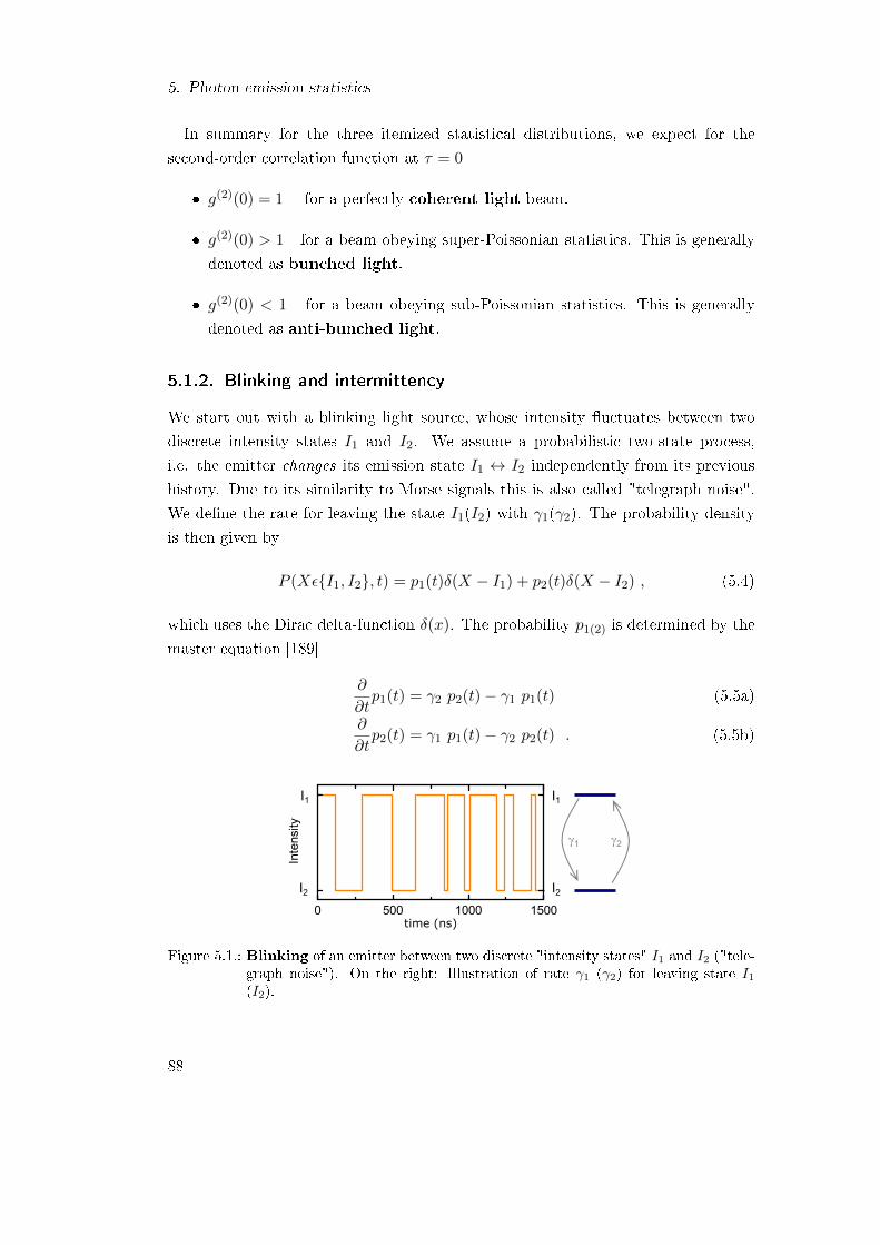
5. Photon emission statistics
In summary for the three itemized statistical distributions, we expect for the
second-order correlation function at τ = 0
g(2)(0) = 1 for a perfectly coherent light beam.
g(2)(0) > 1 for a beam obeying super-Poissonian statistics. This is generally
denoted as bunched light.
g(2)(0) < 1 for a beam obeying sub-Poissonian statistics. This is generally
denoted as anti-bunched light.
5.1.2. Blinking and intermittency
We start out with a blinking light source, whose intensity uctuates between two
discrete intensity states I1 and I2. We assume a probabilistic two-state process,
i.e. the emitter changes its emission state I1 ↔ I2 independently from its previous
history. Due to its similarity to Morse signals this is also called "telegraph noise".
We dene the rate for leaving the state I1(I2) with γ1(γ2). The probability density
is then given by
P (XεI1, I2, t) = p1(t)δ(X − I1) + p2(t)δ(X − I2) , (5.4)
which uses the Dirac delta-function δ(x). The probability p1(2) is determined by the
master equation [189]
∂
∂tp1(t) = γ2 p2(t)− γ1 p1(t) (5.5a)
∂
∂tp2(t) = γ1 p1(t)− γ2 p2(t) . (5.5b)
0 500 1000 1500
Intensity
time (ns)
I1
I2
I1
I2
γ1 γ2
Figure 5.1.: Blinking of an emitter between two discrete "intensity states" I1 and I2 ("tele-graph noise"). On the right: Illustration of rate γ1 (γ2) for leaving state I1(I2).
88

5.1. Theoretical introduction
With the use of arbitrary initial conditions p1(t = 0) and p2(0) = 1− p1(0), we nd
a probability function that solves this partial dierential equation3
p1(t) =γ2
γ1 + γ2+
[p1(0)− γ2
γ1 + γ2
]e−(γ1+γ2)t
p2(t) =γ1
γ1 + γ2−[p1(0)− γ2
γ1 + γ2
]e−(γ1+γ2)t .
(5.6)
For a long time t the probabilities p1(t) and p2(t) converge to the steady-state prob-
abilities:
pinf1 = lim
t→∞p1(t) =
γ2
γ1 + γ2
pinf2 =
γ1
γ1 + γ2.
(5.7)
Assuming the emitter is initialized in state I1 - so p1(t = 0) = 1 - we can now
determine the conditional probabilities to nd it in I1 (I2) after a time delay τ .
Obviously this is invariant under time reversal τ → −τ and we can set τ → |τ |:
p1|1(τ) =γ2
γ1 + γ2+
γ1
γ1 + γ2e−(γ1+γ2)|τ |
p2|1(τ) =γ1
γ1 + γ2− γ1
γ1 + γ2e−(γ1+γ2)|τ | .
(5.8a)
3Exemplarily, we show that this solves the dierential equation (5.5a):
γ2 p2(t)− γ1 p1(t)(5.6)= + γ2
γ1
γ1 + γ2−[p1(0)− γ2
γ1 + γ2
]e−(γ1+γ2)t
− γ1
γ2
γ1 + γ2+
[p1(0)− γ2
γ1 + γ2
]e−(γ1+γ2)t
=
[−γ2p1(0)− γ1p1(0) +
γ2γ2
γ1 + γ2+
γ1γ2
γ1 + γ2
]e−(γ1+γ2)t
=
[−p1(0)(γ1 + γ2) +
γ2(γ1 + γ2)
γ1 + γ2
]e−(γ1+γ2)t
=− (γ1 + γ2)
[p1(0)− γ2
γ1 + γ2
]e−(γ1+γ2)t =
∂
∂tp1(t) .
And fullls the initial conditions
p1(t = 0) =γ2
γ1 + γ2+
[p1(0)− γ2
γ1 + γ2
]= p1(0)
p2(t = 0) =γ1
γ1 + γ2−[p1(0)− γ2
γ1 + γ2
]= 1− p1(0) = p2(0) .
89

5. Photon emission statistics
Correspondingly for initialization in I2 or p2(0) = 1, we nd
p1|2(τ) =γ2
γ1 + γ2− γ2
γ1 + γ2e−(γ1+γ2)|τ |
p2|2(τ) =γ1
γ1 + γ2+
γ2
γ1 + γ2e−(γ1+γ2)|τ | .
(5.8b)
The expectation values 〈I(t)I(t + τ)〉,〈I(t)〉 and 〈I(t + τ)〉 can now be evaluated
explicitly. Since we assumed that the emitter can take only two discrete intensity
states, we just sum up the products of all possible combinations of Ii and their
respective probabilities:
〈I(t)I(t+ τ)〉 =∑i,j=1,2
pinfj Ij pi|j(τ)Ii
〈I(t)〉 = 〈I(t+ τ)〉 =∑i=1,2
pinfi Ii
(5.9)
By using the explicit conditional and steady-state probabilities from Eq. (5.7) and
(5.8), we nd the second order correlation function g(2)(τ) of a blinking emitter with
g(2)(τ) =〈I(t)I(t+ τ)〉〈I(t)〉〈I(t+ τ)〉
= 1 +γ1γ2(I1 − I2)2
(γ1I2 + γ2I1)2e−(γ1+γ2)|τ | . (5.10)
This expression simplies further, if we consider an emitter, which switches between
the two states "on" and "o". This behavior is commonly denoted as emission
intermittency and occurs in the PL of many single molecule or low-dimensional sys-
tems [190]. We set Ioff = 0 and obtain
g(2)(τ) = 1 +γon
γoffe−(γon+γoff)|τ | . (5.11)
Finally, we dene the time constants τi = γ−1i and nd an expression, which was
previously reported in the context of blinking quantum dots [89]
g(2)(τ) = 1 +τoff
τone−(
1τon
+ 1τoff
)|τ |. (5.12)
5.1.3. Single photon emitters
In the preceding considerations a system emitted many photons depending on its "in-
tensity state". We now focus on the emission process itself. Therefore, we modify the
model to analyze the photon emission from a two-level system driven by continuous
excitation, i.e. by a laser beam.
90

5.1. Theoretical introduction
A driven two-level system
We transform the former states I1 to the ground state |g〉 and I2 to the excited state
|e〉. In contrast to the preceding problem, light is only emitted as a single photon
during the transition |e〉 → |g〉 that happens on a characteristic time τ0. The system
is re-excited |g〉 → |e〉 for instance by laser excitation. The mean intensity 〈I(t)〉 isthen equivalent to the expected number of emitted photons. This number is solely
determined by the steady-state probability p|e〉 = pinf2 for the two-level system being
in the excited state |e〉:
〈I(t)〉 = p|e〉(5.7)=
γ1
γ1 + γ2. (5.13)
The same holds true for 〈I(t+ τ)〉.
Referring now to 〈I(t)I(t + τ)〉: As a prerequisite for emission of a photon and
a non-vanishing intensity I(t), the system must be in the excited state |e〉 at a
particular instant of time t. This probability is again given by the steady-state
probability p|e〉. At t the system decays instantaneously to the ground state |e〉 byemitting a photon. The probability for emitting a second photon at t+ τ is given by
the conditional probability p|e〉||g〉(τ) = p2|1(τ). Thus, we can write:
〈I(t)I(t+ τ)〉 = p|e〉 p|e〉||g〉(τ)(5.7),(5.8)
=
(γ1
γ1 + γ2
)2
(1− e−(γ1+γ2)|τ |) . (5.14)
Using both expressions, the second-order correlation function g(2)(τ) for a driven
two-level system reads as
g(2)(τ) =〈I(t)I(t+ τ)〉〈I(t)〉〈I(t+ τ)〉
=
(γ1
γ1+γ2
)2(1− e−(γ1+γ2)|τ |)(γ1
γ1+γ2
)2 = 1− e−|τ |τ0 . (5.15)
This holds true as long as we consider only spontaneous emission from the excited
state to the ground state, which is always the case in our experiments. Here, the
spontaneous emission time τ0 equals the exciton lifetime.
N independent single photon emitters
Finally, the photon statistics of N identical, statistically independent single photon
emitters is evaluated. Their mean intensity is just the sum of all single emitter
91

5. Photon emission statistics
intensities
〈IN (t)〉 = N〈I(t)〉 (5.16)
whereas the correlation intensity is given by pairwise combination of two photons
that could originate from any emitter
〈IN (t)IN (t+ τ)〉 =N∑i=1
p|e〉i
N∑j=1
p|e〉j ||g〉i . (5.17)
If we assume that the emitters are statistically independent, the sum over j facilitates
since we can distinguish two cases (of correlating photons from dierent or from the
same emitter):
p|e〉j ||g〉i = p|e〉 for i 6= j
p|e〉j ||g〉i = p|e〉j ||g〉j = p|e〉||g〉 for i = j(5.18)
Writing the sums in Eq. (5.17) explicitly gives
N∑i=1
p|e〉i
N∑j=1
p|e〉j ||g〉i =
N∑i=1
p|e〉i((N − 1)p|e〉i + p|e〉i||g〉i)
= N (N − 1)p|e〉p|e〉 +Np|e〉p|e〉||g〉 .
(5.19)
Comparing this with Eq. (5.13) and (5.14), we obtain
〈IN (t)IN (t+ τ)〉 = N (N − 1)〈I(t)〉2 +N〈I(t)I(t+ τ)〉 . (5.20)
Thus, the second-order correlation function for N identical but statistically indepen-
dent emitters is given by
g(2)N (τ) =
〈IN (t)IN (t+ τ)〉〈IN (t)〉〈IN (t+ τ)〉
=N (N − 1)〈I(t)〉2 +N〈I(t)I(t+ τ)〉
N 2〈I(t)〉〈I(t+ τ)〉
=N − 1
N+
1
N(1− e−
|τ |τ0 ) .
(5.21)
5.1.4. Photon emission statistics of blinking carbon nanotubes
At low temperature CNTs exhibit non-classical photon statistics, i.e. the anti-
bunching of photons [76, 77, 127]. Additionally they are aected by charge uctua-
92

5.1. Theoretical introduction
-50 0 500
1
2
g(2) (τ
), pu
lsed
τ(ns)
-50 0 500
1
2
g(2) (τ
), cw
τ(ns)-50 0 500
1
2τon =τ
off =100ns
τon =2τ
off =100ns
2τon=τ
off=100ns
g(2) (τ
)τ(ns)
-2 0 20
0.1
τ(ns)
(a)
(c) (d)
(b)
η
Figure 5.2.: Expected photon statistics: (a) Simulated photon statistics of a blinkingsingle photon emitter under pulsed excitation (f−1 = 1
76 MHz ≈ 13 ns) showingphoton anti-bunching (lower dashed line) superimposed with photon bunching(upper dashed line). The spontaneous emission lifetime was tau0 = 3 ns, theblinking times to τon/off = 100 ns and anti-bunching contrast to 1−η = 0.95. (b)
Zoom in to τ = 0 shows the discrepancy between η = 0.05 and g(2)(0) = 0.1.(c) Photon statistics using the same parameters but a continuous excitationscheme. (d) g(2)(τ) for continuous excitation or envelope for pulsed excitationwith dierent characteristic blinking times. Compared to a non-blinking emitter,g(2)(τ) is exaggerated up to 2.5 for τon = 2τoff = 100 ns.
tions in their environment leading to long term intensity uctuations varying from a
few 100 ns up to hours. Since the typical time scale of blinking τon/off is far beyond
the exciton lifetime τ0 - even in the cleanest CNTs - we can keep both processes
decoupled. Taking the product of Eqs. (5.12) and (5.15), g(2)(τ) of an individual
CNT is given by
g(2)(τ) =
(1 +
τoff
τone−(
1τon
+ 1τoff
)|τ |)(
1− e−|τ |τ0
). (5.22)
In order to proof that a non-blinking emitter is a single-photon emitter, it is sucient
to consider g(2)(τ = 0). The threshold for a single photon emitter is g(2)(τ) < 0.5.
Due to the superimposed signature of photon-bunching especially for τ = 0 this
does not hold for blinking photon emitters. Rather the inuence due to the blinking
condition has to be separated from the single emission process. Accounting for this,
93

5. Photon emission statistics
we introduce a contrast factor η that is dened as
η :=g(2)(τ)
1 + τoffτon
e−(
1τon
+ 1τoff
)|τ |
=g(2)(τ = 0)
1 + τoffτon
. (5.23)
For a non-blinking emitter (τoff = 0) this just equals g(2)(0). Therefore the threshold
for single photon emission is again η < 0.5. The discrepancy between g(2)(0) and η
is illustrated in Fig. 5.2, which shows the simulated photon statistics expected from
a blinking single photon emitter.
5.2. Hanbury-Brown and Twiss interferometer
5.2.1. Basic considerations
Proposed by Hanbury-Brown and Twiss [191] for astronomical application, their in-
tensity correlating interferometer (HBT) has become an important tool for quantum
optics since the rst experimental proof of photon anti-bunching from single atoms
by H.J. Kimble et al. [192]. The principle of an HBT interferometer is as follows. An
incoming light beam is split into two paths (of same intensity in an ideal case). The
intensity of each path is detected separately and then correlated. Hanbury-Brown
and Twiss demonstrated that this correlation can be a linear multiplication of the
intensity uctuation or a coincidental measurement that counts the simultaneous
arrival of photons on each detector.
For quantum optical application single photon counters (SPC) are widely used
because they feature a high temporal resolution (∼ 350 ps) and are sensitive to
single photons. Thus, they are highly suitable for measuring the Fock state of a light
beam [187]. An SPC generates a digital electric pulse whenever at least one photon
is detected. After detection, it exhibits a dead-time τdead, during which it cannot
detect another photon. In order to correlate the two paths, a detection event on the
SPC in path 1 triggers the "start" of an electronic time clock. A subsequent detection
event on the SPC in path 2 triggers "stop". This scheme allows for determination of
the time dierence τ between two consecutively incident photons and is particularly
capable to resolve τ < τdead, which is impossible for a setup using a single detector
only.
The statistical distribution of τ is revealed in histograms that cumulate the time
dierences from many repeated measurements. Under certain conditions the second-
94

5.2. Hanbury-Brown and Twiss interferometer
0 100 200 300 400
0.6
0.8
1.0
Nor
m. o
ccur
renc
eτ(ns)
r1 = r2
= 8·105 cts
s-1
Figure 5.3.: Normalized correlation histogram of an intense pulse light source illus-trates a weak saturation eect. The orange solid line displays the theoreticallyexpected probability distribution r
flaser. However, the respective count rates r1/2
exceeded typical count rates gained from an individual CNT by far. Thus, thissaturation eect becomes negligible for the here presented experiments.
order correlation function g(2)(τ) (see Chap. 5.1) can be simply determined by nor-
malization of these histograms. This requires [193]:
The average time between two photons must be larger than the dead time of
the SPC detectors.
The investigated light source must not emit too many photons at once.
The count rate must be adapted to the period of interest.
The following considers all these conditions. First of all we dene the average count
rate ri, which is the temporal mean of photons detected by detector i per time unit.
Typically SPCs feature dead-times τdead below 70 ns. Hence, the rst condition is
fullled as long as r < 14 ·106 cts s−1. This was the case in our experiments as count
rates never exceeded 2 · 103 cts s−1.
Also the second condition was trivially fullled. As we will show below, the PL
of individual CNTs at cryogenic temperatures featured characteristic photon anti-
bunching, so that a CNTs emits typically photons one by one [76,77]. Of course, only
a smaller fraction of these photons were detected. From such a source we expect all
correlation events at |τ | > 0 and especially no saturation eects, which would occur
for a very intense pulsed light beam. Additionally, placing the setup in a light-tight
box and spectral ltering the PL light reduced background counts well below the
intrinsic dark count rate of the used SPCs.
Only the third condition deserves a closer inspection, especially since the range of
interest is much higher for investigation of a blinking emitter (typically 500-1000 ns)
than for the proof of photon anti-bunching where a range of ±30 ns is sucient [76].
First, we will illustrate matters in a probabilistic approach. In order to create a
95

5. Photon emission statistics
correlation event at τ in an HBT interferometer, it is not sucient that two photons
are incident on each SPC within the time interval τ . Rather after the rst photon
triggers "start", no other (third) photon is allowed to trigger "stop" before the second
photon does. Therefore the probability to detect correlation with a big time delay
is lower than the probability for the detection of a small time delay. In practice no
correlation event with τ > 1 h will be detected, although g(2)(τ = 1 h) = 1 in all
known cases.
We examine a pulsed light source (repetition frequency flaser) that creates an
identical average count rate on each detector (r = r1 = r2). The probability to
detect a correlation for the kth pulse is then given by
P (k) =r
flaser
(1− r
flaser
)|k|. (5.24)
To illustrate this saturation we measured the correlation of an intense pulsed laser
beam with a count rate of 8·105 cts s−1 and a repetition frequency of 76.0 MHz. The
count rates (normalized to τ = 0) are depicted in Fig. 5.3. The solid line displays
the theoretical probability normalized to r/flaser. In our experiments typical count
rates did not exceed 2000 cts s−1. For such low count rates the detection probability
is only negligibly varied for τ < 1000 ns (or using pulsed excitation for the rst 76
fringes of the histogram). In detail, the probability for correlating two photons from
the same pulse P (k = 0) is only two tenth percent higher than the probability for
correlating two photons separated by 1000 ns4:
P (k = 75) = 0.9980 · P (k = 0) . (5.25)
In summary, we fulll all conditions to evaluate g(2)(τ) from normalization of the
measured histograms correlating only two consecutive photons.
For faint PL signals we further used pulsed excitation to increase the signal-to-
noise ratio. In consequence, this concentrates detection events to τ = 0 and multiples
of the excitation pulse frequency instead of accumulating correlations for all possible
values of τ . Compared to continuous excitation, it allows for faster determination of
the characteristic blinking times τon/off and of the anti-bunching contrast 1− η.
4P (75) =(
1− 2000 cts s−1
76 MHz
)75
≈ 0.9980
96

5.2. Hanbury-Brown and Twiss interferometer
5.2.2. Hanbury-Brown and Twiss interferometer setup
Single photon detectors
Silicon avalanche photodiodes (APD) are sensitive to single photons in a broad spec-
tral range from the visible to the near infrared region [194]. Used in the Geiger mode
- when the diode is highly reverse biased - a photon excites a single electron, which is
accelerated to the diode's n-layer. During acceleration this electron excites secondary
electrons from the intrinsic layer, which starts an avalanche process and results in a
measurable current. This sudden gain of an avalanche current after incidence of a
single photon allows the detection of single photons with an accuracy below 400 ps.
Continuing the avalanche process would lead to gigantic current, which could harm
the diode. Hence, shortly after occurrence of a detection event a control electronic
reduces the bias voltage and stops the avalanche process. The time for stopping the
avalanche process and re-biasing the diode adds up to a dead time of typical 70 ns
after every detection event.
We employed two dierent APD models that will be compared in the context of
APD cross talk later in this chapter. The rst type was manufactured by PicoQuant5
(PQ) and will be termed as PQ APD in the following. The second type was by Perkin
Elmer6 (PE) in the following PE APD. One of the PE APDs featured an FC ber
coupler placed before the optically active area. However, it could be also used in a
free space setup provided that the beam was focussed appropriately.
Optical layout
Fig. 5.4 schematically depicts the setup of the used HBT interferometer, which was
placed in a light-tight box. The optical signal was sent in via a single-mode ber
(SM7) and coupled to free space with a ber coupler FC18. The collimated beam was
split at a 50:50 beam splitter (BS)9 and each half was imaged on the optically active
area of one APD by the lenses L1 and L210, respectively. In order to reduce cross talk
between both APDs, the collimated beams were not focused on the optically active
areas but illuminated them as much as possible. In detail, this is discussed later5τ−SPAD-20 by PicoQuant GmbH, Berlin, Germany6SPCM-AQHR-15 by Perkin Elmer Optoelectronics, Vaudreuil, Canada7single-mode ber SM800 specied for 830 nm: SM800 5.6/125/245 by Diamond GmbH, Echter-dingen, Germany
8Coupling lens: focal length f = 11 mm; C220TME-B by Thorlabs9BS010 by Thorlabs. The beam splitter is mounted on a ip mount. This allows to swing it outof the beam so all light is focussed on APD 1 only. This makes the setup versatile for otherapplications.
10focal length f = 18.4 mm; C280TME-B by Thorlabs
97

5. Photon emission statistics
CCD
APD 1
APD 2
APD 2
multi
mode fiber
free
space
input
FC1
FC2
SM
MM
LCCD
L1
L2
PicoHarp300
τ
or
stop
start
τ
BS
Figure 5.4.: Schematic setup of the intensity interferometer: The alternative opticalpaths for free space and ber based coupling to APD 2 are depicted in thedashed boxes.
in this chapter. We monitored the imaging directly using an auxiliary laser beam,
whose light (reected from the APDs) was imaged on a CCD camera11. This path was
employed for setup adjustment only and blocked for all correlation measurements.
As we will discuss later, a setup conguration that showed minimized cross talk
between both APDs consisted of a multi-mode ber12 that was directly connected
to the ber coupler of an PE APD. Both free space and ber based realizations are
shown in the dashed boxes in Fig. 5.4.
The electrical signals of both APDs were correlated by a time-correlation box13,
which featured an variable accuracy down to 4 ps for measuring the time dierence
between two pairwise voltage pulses. The box's standard software integrated the
correlation events for an integration period up to ten hours. However, this setup
could only detect positive values of τ . That means, the "start" input must arrive
before the "stop" input. To shift the measurement range to negative values, a delay
was added on the "stop" signal. This delay was realized by an elongated cable from
APD 2 to the correlation box.
11focal length f(LCCD) = 100 mm12core diameter 62.5 µm by Thorlabs13PicoHarp 300 by PicoQuant GmbH, Berlin, Germany
98

5.2. Hanbury-Brown and Twiss interferometer
5.2.3. Reducing the cross talk
During the avalanche eect an APD itself emits photons in a breakdown ash due
to electroluminescence [195]. This ash is insignicant if the APDs are suciently
distant from each other (space-like separated) or when only a single APD is used
(like in measurements on the exciton lifetime discussed in Chap. 5.3.4). However, the
APDs in the described setup were not space-like separated. Rather the breakdown
ash of one APD reached the other within the range of interest and triggered falsied
correlation events. This crosstalk can not be regarded as a minor artefact. First, it
reduces the rate of signicant correlation events. Further, it could become a limiting
factor in the detection of possible fast intensity uctuation (see Chap. 5.1.2).
Fig. 5.5(a) depicts the integrated cross talk events between two APDs in our
HBT setup that were operated for 10 hours in complete darkness. We found two
accumulation points for correlation events for τ ≈ ±5 ns. This corresponded to
c · 5 ns ≈ 1.5 m, which equals the optical path length from one APD to the ber
coupler and back to the second APD. By covering the ber coupler FC1 with a
nonreective opaque beam block, we completely suppressed the cross talk between
both APDs as illustrated by only ve correlation events in 10 hours (orange bars in
Fig. 5.5(a)).
We measured the spectrum of the breakdown ash by using a 50:50 ber beam
splitter connected to the ber input of the HBT box as depicted in the inset of
Fig. 5.5(b). We inserted a faint laser beam with a wavelength of λexc = 850 nm
through the beam splitter into the HBT input. This increased the rate of detection
events and thereby the overall intensity of the breakdown ash. The exit of the beam
splitter was connected to a spectrometer (see Chap. 3.1.2). We used a 900 nm long
pass lter (blocking region marked as grey area) in front of the spectrometer to lter
out any laser light. In accord with previous reports [195,196] we nd the wavelength
of the ash broadly distributed in the detection range with a small local maximum
around 980 nm. Surprisingly, the intensity of the breakdown ash was ve times
higher for the PQ APDs compared to the PE APDs as illustrated in Fig. 5.5(b).
Knowing its origin, we now took several measures against APD cross talk. As a
measure of cross talk, we quantied the share of falsied correlation events in all
correlation events. In a photon correlation measurement of a pulsed laser beam we
compared the rate of falsied correlation events nfalse (blue area in Fig. 5.5(c)) with
the rate of correct correlation events at τ = 0 termed as ncorrect (orange area). We
did this for various laser intensities. As a measure for the laser intensity we took
the count rate rlaser of APD 1 (not the correlation rate between both) and kept this
99

5. Photon emission statistics
104 105
100
101
102
103
-20 0 200
5
10
15
Occ
urre
nce
(cts
/10
h)τ(ns)
-20 0 200
50
100
150
Occ
urre
nce
(cts
/600
s)
τ(ns)
n fals
e/co
rrec
t (ct
s/s)
nLaser
(cts/s)
900 950 10000
1
Inte
nsity
(cts
/103 s
)
Wavelength (nm)
(a) (b)
(c) (d)
λexc
=850nm
2·c·1.5m LPPE/PQ
PQPE
Figure 5.5.: Cross talk between avalanche photo-detectors (a) recorded in a corre-lation measurement in complete darkness (black histogram). The correlationevents are triggered by photon or thermal noise and vanish when the ber cou-pler FC1 was covered (orange histogram). (b) Spectrum of the breakdown ashfrom Perkin Elmer (PE) and PicoQuant (PQ) APDs recorded by a setup shownin the inset. A faint laser beam triggered more counting events and thus in-creased the ash intensity. (c) Photon correlation measurement of a laser beamwith nlaser = 6, 000 cts s−1. The number of correct (falsied) correlation eventsis shaded orange (blue). (d) Rates for falsied and correct correlation eventsas a function of the laser intensity showing linear and quadratic dependence,respectively.
rate small enough that saturation eects due to the APD dead time were negligible.
A correlation event is a two-photon process because each APD is triggered by one
photon. As expected for such a process we found a quadratic dependence of ncorrect
on rlaser (Fig. 5.5(d)). The detection eciency given by ncorrect/r2laser. In contrast,
a single photon is sucient to trigger a falsied correlation event so we nd ncorrect
as a linear function of rlaser. The cross talk rate is then ncorrect/rlaser.
All taken measures are a trade-o between cross talk rate and detection eciency.
Tab. 5.1 summarizes our progress. For a HBT setup using two PQ APDs we reduced
the cross talk rate by a factor of two. Here, the laser spot illuminated the entire
optically active area instead of being focussed on it. As the entire laser spot still
tten onto the active area, the detection eciency was unaected.
If we further used the PE APDs instead of the PQ APDs, we found again a
100

5.3. Freely suspended carbon nanotubes
APD type layout detection eciency cross talkncorrect/n2
lasernfalse/nlaser
(in 10−8 s/cts) (in 10−4)
PicoQuant (PQ)spot focused 1.026 10.4
spot maximized 1.024 6.6
Perkin Elmer (PE)spot maximized 1.14 2.8multi-mode ber 0.57 0.01
Table 5.1.: Detection eciency and cross talk for dierent layouts of the HBT box. Forthe free space setup conguration the detection eciency is constant regardlessof the APD type. Expanding the spot size and using a multi-mode ber forspatial ltering reduces the cross talk by a factor of 1000. In return, attenuatedtransmission through the ber reduces the detection eciency by 0.5.
considerably reduced cross talk. This conrms our ndings from the breakdown ash
spectra of each APD model (Fig 5.5(b)). PQ APDs exhibit generally an increased
breakdown ash intensity. In both measurements we consistently identied that the
breakdown ash intensity of PQ APDs exceeded those of the PE APDs by a factor
of ve.
One of the PE APDs featured already a ber connector that could be only used
with an additional focussing lens in a free space setup. In a more elegant layout we
coupled one arm of the HBT setup in a multi-mode ber (core diameter 62.5 µm),
which provided for ideal imaging on the active area. In addition, the ber acts as a
spatial lter and suppressed overwhelmingly the cross talk rate by a factor of 280.
In return, the transmission loss due to coupling in a ber was almost 30 percent,
which reduced the detection eciency by roughly 50 percent. For all correlation
measurements presented in this thesis, we employed this layout with a multi-mode
ber.
5.3. Freely suspended carbon nanotubes
The previous chapters presented indication that many detrimental spectroscopic fea-
tures of CNTs arise from the interaction with the environment. Spectral wandering
was assigned to interaction with close charge uctuators (see Chap. 4.3) and also
localization potentials and excitation spectra were identied as presumably sensitive
to close charge impurities (see Chap. 4.7). In a second approach for studying the
localization of excitons we focus on the isolation of individual CNTs from their en-
vironment. With except of their suspension points, freely suspended CNTs are not
in contact with any dielectric material as illustrated in Fig. 5.6(c). Such samples
101

5. Photon emission statistics
could not be manufactured from spin-coating of a commercial CoMoCat solution.
Rather, we grew CNTs directly over the trenches of a perforated substrate using a
chemical-vapor-deposition (CVD) process. A detailed study considering growth of
CVD CNTs was presented in the diploma thesis of M. Hofmann [91].
In the following, we discuss the optical properties of individual as-grown suspended
CVD CNTs at cryogenic temperature (T = 4.2 K). These results were also published
in Ref. [127]. We give a brief overview on the preparation of as-grown suspended
CVD CNTs. Then, their optical properties are compared to sc encapsulated CoMo-
Cat CNT dispersed on a Si-SiO2 substrate. In particular, we discuss experiments
that consider exciton lifetime, photon anti-bunching and fast intermittency processes.
The two sample layout are illustrated in Fig. 5.7, which also presents complemen-
tary images from both layouts. We identied locally conned PL emission from sc
encapsulated CoMoCat CNT dispersed on a Si-SiO2 substrate (left panels) and from
as-grown suspended CVD CNTs (right panels). In addition, we will discuss a third
layout that features CVD CNTs grown on a SiO2 substrate that is not depicted here.
5.3.1. As-grown suspended CNTs
CNT material, which will be termed as CVD CNTs in the following, was synthesized
by chemical-vapor-deposition (CVD) in a standard CVD furnace. The growth was
assisted by a bimetallic iron-ruthenium (FeRu) catalyst. The catalyst particles were
deposited on carrier substrates from a FeRu suspension either by spin or by drop
coating. For synthesis of CNTs the samples were heated to 850°C in an Ar/H2 (95%-
5%) gas mixture and then kept in a constant ow of 1 slm methane and 0.75 slm
hydrogen for 10 minutes before allowing to cool down in a hydrogen and Ar/H2 gas
ow. The growth procedure was optimized to yield a CNT density below 1 µm2 and
narrow-diameter nanotubes with a mean diameter below 1 nm. Diameter distribu-
SiO2
individual CNT
SiSi3
N4
(c)
CVD CNT
(b)
SiO2
NiCr
Al2
O3
Vg
d2
p++- Si
d1
CoMoCat
CNT
SiO2
Si
individualized CNT layer
(a)
CoMoCat
CNT
Figure 5.6.: Sample layouts III: CoMoCat CNTs on a silicon oxide surface, which featuresa metallic grid (a). CoMoCat CNTs embedded in an electric gate device (b).CVD CNT freely suspended over a crater (c).
102

5.3. Freely suspended carbon nanotubes
(f)(e)
(a) (b)
(d)(c)
Figure 5.7.: CoMoCat CNTs on substrate (left panels) and as-grown suspendedCVD CNTs (right panels): (a-b) Schematic illustration. (c-d) SEM imageof a sample section. The scale bar measures 1 µm. (e-f) Complementary microPL maps of the same sections revealed spatially conned PL emission.
tions were obtained by tapping-mode atomic force microscopy on samples with CVD
CNTs fully supported by a Si-SiO2 substrate. Such samples with as-grown CVD
CNTs in contact with SiO2 were used as reference material for density and diameter
distributions as well as in cryogenic spectroscopy. Suspended CNTs were synthesized
on commercial grids typically used in transmission electron microscopy (TEM). The
specic grid used in the experiments was perforated with holes of 2 µm diameter and
a pitch of 4 µm and coated with ∼ 100 nm of SiO2 by plasma enhanced CVD. The
grids provided for suspension of nanotubes in the region where the hole-perforated
Si3N4 membrane was not supported by the underlying Si frame; this region was lo-
cated in the center of the TEM grid. However, the Si carrier frame supported the
SiO2-Si3N4 membrane at its edges. With scanning electron microscopy (SEM) we
identied CNTs suspended over the full diameter of the crater as well as CNTs that
were suspended only near the walls of the crater. Also the latter exhibited partly
suspended segments at the perimeter of the crater.
103

5. Photon emission statistics
5.3.2. Methods
PL spectra of individual CNTs were already discussed in the previous chapters. For
recording of photon emission statistics we used the HBT interferometer without any
spectral ltering. The correlation box allowed to correlate two detection events sep-
arated within 65536 time bins. Due to this xed number of bins the resolution
δτres, which equals the width of each bin, determined the total range of interest
τmax. Therefore, we used a low resolution δτres = 256 − 512 ps in order to extend
the range of interest to longer timescales. In fs-pulsed mode the excitation laser
was operated with a repetition rate of flaser = 76.0 MHz. We controlled the time-
averaged laser power via the power stabilization (bandwidth <10 kHz) presented
in Chap. 3.1.2. However, the maximum power deposited within one fs-laser pulse
exceeded the time-averaged intensity by at least one order of magnitude. In order
to prevent CNTs from bleaching, we reduced the time-averaged intensity by at least
a factor of 3 before switching the laser from cw to fs-pulsed mode. For a signicant
determination of photon emission statistics we integrated between 2 to 10 h. As dis-
cussed in Chap. 5.2.3 signatures of cross-talk were highly suppressed in all correlation
histograms.
Stable PL emission from CVD CNTs routinely allowed for recording of two-photon-
correlations in pulsed and continuous excitation. In contrast, CoMoCat CNTs showed
blinking on all time scales and often inhibited long-lasting recording as required for
signicant statistics of two-photon-correlations. Because of the increased signal-to-
noise ratio, we employed only pulsed excitation to obtain photon emission statistics
of CoMoCat CNTs.
With minor modications on the HBT setup, we determined the photolumines-
cence lifetime of individual CNTs by correlating the signal of a single APD with
the trigger output of the TiSa laser. However, the short lifetime of CoMoCat CNTs
hindered the use of APD photon counters because their time resolution was beyond
typical PL lifetimes of 20-80 ps. To estimate the lifetime of the CoMoCat reference
material we used a streak camera14, which featured a resolution below 5 ps.
5.3.3. Spectral properties
Compared to the PL spectra of CoMoCat CNTs, the narrow line width is the rst
striking dierence in the PL of individual CVD CNTs as illustrated in Fig. 5.8. Such
narrow optical line widths are unusual for CNTs, even at cryogenic temperatures
14C5680 by Hamamatsu
104

5.3. Freely suspended carbon nanotubes
0
30
60
90
Tim
e (s
)
103.8
144.8
min
max
PL in
tens
ity
x10
-5 0 50
50
Tim
e av
erag
ed P
L(c
ts/s
)
x6 x5
-5 0 5
Spectral shift (meV)
x2
0
100
Occ
urre
nce
-5 0 5
0
1
1.32 1.33
PL in
tens
ity (a
. u.)
1.40 1.41
Energy (eV)
1.395 1.405
(a) (b) (c)
(d) (e) (f)
(g) (h) (i)
Figure 5.8.: Spectral properties of suspended CVD CNTs (right column) in compari-son with CVD CNTs on a SiO2 substrate (middle column) and CoMoCat CNTson a SiO2 substrate (left column): (a-c) Spectra recorded with an integrationtime of 1 s. (d-f) PL traces featuring spectral jumps and wandering. (g-i) PLenergy histograms (in orange) and spectra recorded with 100 s integration (bluetraces). (Adapted from Ref. [127])
[60, 76, 197]. For reference we studied as-grown CVD CNTs in contact with SiO2 as
well as commercial CoMoCat CNTs dispersed on SiO2 (discussed in Chap. 3). Under
similar experimental conditions, CoMoCat CNTs typically exhibited asymmetric PL
proles [59, 76, 197] with line widths of a few meV, one order of magnitude broader
than our CVD-grown nanotubes in 1 s integration time.
On longer experimental timescales, the line width of the time-averaged PL broad-
ened even further for suspended CNTs as illustrated the spectra of Fig. 5.8(g,h).
However, suspended CVD CNTs showed no change in the emission prole, irrespec-
tive of the integration time. The eective integration time of Fig. 5.8(i) was 100 s, but
same hold true for up to several days of observation. The PL time traces in Fig. 5.8(d-
105

5. Photon emission statistics
f) reveal that spectral wandering was responsible for the broadening of the optical
line width on a meV energy scale, in accord with previous reports [76, 134, 197]. At
the same time, it also accounted for the apparent ne structure [60,134] and, to some
extent, for the asymmetry in the spectral prole as illustrated in the histograms of
Fig. 5.8(g-i). For small integration times CVD CNTs fully supported by a Si-SiO2
substrate featured narrow emission line as exemplied in Fig. 5.8(b). However, in
the course of integration these CNTs developed an asymmetric peak accompanied
by a satellite as shown in Fig. 5.8(h), which corresponds to time-averaging of the
PL trace depicted in Fig. 5.8(e)). For suspended CNTs, such detrimental features as
spectral wandering were not observed.
5.3.4. Photoluminescence lifetime
In contrast to previous reports we found decay times on the scale of nanoseconds for
all suspended CNTs. This is one order of magnitude longer than for the CoMoCat
reference material as illustrated by red versus black circles in Fig. 5.9(b). A PL
decay trace for a single suspended CVD CNT with a monoexponential decay time of
3.35 ns is shown in Fig. 5.9(a). Previous room-temperature experiments determined
both monoexponential and biexponential decays depending on material quality, with
photoluminescence decay times of the order of tens of picoseconds [198]. Similar
results were obtained at low temperatures [122]. The discrepancy between the 10-
100 ps PL lifetimes observed experimentally and the radiative exciton lifetimes of
1-10 ns predicted by theory [33, 64, 65] is attributed to rapid non-radiative decay of
mobile excitons encountering quenching sites (Auger processes) [61].
The long PL lifetimes in our suspended CVD CNTs indicate that excitons were
protected by localization from exploring quenching sites. PL lifetimes on the scale
of nanoseconds are in agreement with the radiative lifetimes estimated for excitons
with coherence lengths in the range between the exciton Bohr radius of 1.2 nm in
narrow-diameter CNTs [34] and the optical wavelength, as depicted by solid lines in
Fig. 5.9(b). We estimate the intrinsic radiative lifetime τ of CNT excitons as [33,65]
1
τ=
√εe2E2
11f
2πε0m0~2c3, (5.26)
using the free electron massm0 and ε = 1.846 for the surrounding vacuum. f denotes
the oscillator strength per carbon atom and is given by 0.014 eV−1E11dtσc/A where
A is the area per carbon atom A = 3√
34 a2
cc and σc the connement length in units
of the exciton Bohr radius αB [34].
106

5.3. Freely suspended carbon nanotubes
0 5 10100
101
102
103
Inte
nsity
(cts
)
Time (ns)
τ0 = 3.4 ns
1.30 1.35 1.40 1.45
0.1
1
10
τ 0 (ns)
PL energy (eV)
T = 4.2 K
(a) (b)
Figure 5.9.: Exciton lifetime in suspended CVD CNTs: (a) The PL intensity of sus-pended CVD CNTs as a function of time (black solid line) showed an mono-exponential decay (here exciton lifetime τ0 = 3.4 ns, t illustrated as orangesolid line). (b) These exciton lifetimes (orange circles) exceed those typicallyobserved in CoMoCat CNTs (blue circles) by at least one order of magnitude andagree with the estimation of the intrinsic exciton lifetime, which is illustratedby the grey solid lines. (Adapted from Ref. [127])
Moreover, localization is also responsible for narrow emission proles by inhibiting
diusive exploration of inhomogeneities along the tube axis that would give rise
to line broadening via dephasing. Taking the resolution limit of our spectrometer
as a conservative value for the total line width, we arrive at 15 ps for the lower
bound to the exciton coherence time in CNTs at 4.2 K. Further support for exciton
localization is given by the now following discussion of the photon emission statistics.
Like reported on CNTs at low temperatures [76,77], also the PL from freely suspended
CVD CNTs featured non-classical photon emission.
5.3.5. Photon emission statistics
Fig. 5.10 depicts spectra and photon emission statistics of both a CoMoCat CNT on
substrate (upper panels) and a suspended CVD CNT (lower panels). It exemplies
broad and asymmetric PL emission proles of CoMoCat CNTs contrasting the narrow
emission lines of freely suspended CVD CNTs. The photon emission statistics of
both CNTs featured non-classical light emission, i.e. photon anti-bunching as proven
by the missing central peak at τ = 0. In addition, the CoMoCat CNTs showed
signicant signatures of photon bunching due to fast intermittency.
107

5.Photonem
issionsta
tistics
1.34 1.360
20
40
Inte
nsity
(cts
s-1 µ
W-1)
1.38 1.400
100
200
PL energy (eV)
0 100 200 3000.0
0.5
1.0
1.5 Occ
urre
nce
τ (ns)
0 100 200 3000.0
0.5
1.0
1.5
g(2) (τ
) 0
50
100
150
0
50
100
-20 -10 0 10 20
0.0
0.5
1.0
1.5
g(2) (τ
)
-20 -10 0 10 200.0
0.5
1.0
1.5
τ (ns)
(a) (b)
(d) (e)
(c)
(f)
Figure 5.10.: Spectra and photon emission statistics of CoMoCat CNTs (upper panels) and as-grown suspended CVDCNTs (lower panels): (a) Spectrum of a CoMoCat CNT recorded with continuous excitation featuring a single asymmetricemission line with a line width of 5.1 meV. (b) Photon statistics of the same tube recorded in 10 hours with pulsed excitation(black solid line) that reveals signatures of photon anti-bunching (missing peak at τ = 0) and photon bunching (exponentialdecay). The orange solid line displays a t according to Eq. (5.22) with η = 0.87, τon = 343 ns and τoff = 160 ns. (c) Zoom into τ = 0. (d) Spectrum of a suspended CVD CNT featuring a single narrow emission line below the spectrometer resolutionlimit of 40 µeV. (e) Photon statistics of the same CNT recorded in 10 hours with pulsed excitation (black solid line) andcontinuous excitation (grey solid line), respectively. Both histograms show photon anti-bunching without any signatures ofphoton-bunching for τ > τ0. The orange solid line displays a t according to Eq. (5.22) with η = 0.89 and τ0 = 3.3 ns butdiverging values for τon →∞ and τoff → 0. (f) Zoom in to τ = 0.
108

5.3. Freely suspended carbon nanotubes
We used a standard tting routine to normalize the histograms (as discussed
in Chap. 5.2.1) and to t Eq. (5.22), which is depicted as orange solid lines in
Figs. 5.10(b,d). This gave the characteristic blinking times τon/off , the anti-bunching
contrast η and in case of CVD CNTs the PL lifetime τ0 (see Eq. 5.23). For the tting
of pulsed histograms from CoMoCat CNTs we set τ0 = 1 ns. For the CVD grown
suspended CNTs we were also able to record signicant photon emission statistics in
continuous excitation (grey solid line in Fig. 5.10). For the CNT depicted here we
found τ0 ≈ 3.3 ns and conrmed directly the extremely long lifetime of excitons in
this material.
Intermittency
All CoMoCat CNTs featured photon-bunching superimposed on signatures for single
photon emission. In the picture of a blinking single-photon emitter, which switches
between a dark and an emitting state, we identied characteristic times τon(τoff) in
a range of 70-310 ns (50-680 ns). Similar results were previously reported for CNTs
embedded in PMMA15 [77]. Fig. 5.11(b) depicts the characteristic time in the "on"-
state τon as a function of the characteristic time in the "o"-state τoff . In agreement
with reports on blinking CNTs [77] as well as for self-assembled quantum dots [89],
τon and τoff diered not more than by a factor of 2, which is indicated by the blue
shaded area in Fig. 5.11(a).
Photon-bunching signatures on a time scale of a few 100 ns were interpreted as a
new aspect to intermittency [77]. These occur in addition to the general charging
induced power-law blinking, we discussed in Chap. 4.3, and to intermittency caused
by the activation of recombination centers [199].
In contrast, the photon emission statistics of as-grown suspended CVD CNTs
did not exhibit such signatures of bunched photons. We found best conformance
with our theoretical model given in Eq. (5.22) for diverging values of τon → ∞ and
τoff → 0. This supports our ndings that suspended CVD CNT featured blinking-free
PL emission signal even on the shortest timescales. Due to isolation from external
uctuations and to ineective occupation of the lower energetic dark state, as-grown
suspended CVD CNTs were intrinsically bright.
Photon anti-bunching
For all investigated CNTs (regardless if CoMoCat or CVD) we identied evidence
for photon anti-bunching. Fig. 5.11(b) summarizes for all CoMoCat CNTs inves-15poly (methyl methacrylate)
109

5. Photon emission statistics
1.30 1.35 1.400.0
0.5
100 500
100
500
τ on (n
s)τ
off (ns)
1−η
Emission energy (eV)
(8,3) (9,1) (6,4)(a) (b)
Figure 5.11.: Time-resolved properties of CoMoCat CNTs: (a) Without exceptionthe photon emission statistics of CoMoCat CNTs featured photon bunching,which is associated to PL intermittency. Depicted are characteristic times"on" state τon as a function of τoff , which indicate that both dier only by afactor of 2 (equivalent to the blue shaded area). (b) Anti-bunching contrast1−η for all recorded CoMoCat CNTs was below the threshold of 0.5 indicatingsingle-photon emission.
tigated their anti-bunching contrast η as a function of the respective PL energy.
All values were well below the threshold for unambiguous single-photon emission
of η = 0.5. This non-classical photon emission of CNTs at cryogenic temperature
has been reported previously [76, 77] and equals the photon emission statistics of
quantum-dots. However, its physical origin is still arguable. Two possible mecha-
nisms are discussed [76]:
First, exciton-exciton annihilation is highly ecient in CNTs [200]. Further, the
diusion length of CNT excitons has been reported with more than 610 nm [67] at
room temperature and is prospected to increase considerably at cryogenic temper-
ature [111]. After excitation of an exciton ensemble, highly mobile excitons would
recombine non-radiatively, so that a CNT could end up at most with a single exciton
only. Exciton-exciton annihilation is typically responsible for saturation eects in
the emission of mobile CNT excitons [201]. However, also at high excitation intensi-
ties photon anti-bunching was observed in CoMoCat (see Ref. [76]) and CVD CNTs
(see Fig. 5.12). As the rate of exciton-exciton annihilation is only reasonably higher
than the PL rate, ecient exciton-exciton annihilation of delocalized CNTs cannot
explain photon anti-bunching in even saturated PL signals.
A second possible mechanism is based on the formation of localization sites (CNT
quantum dots). Although experimental indication for the existence of biexcitonic
states in CNTs were reported [202], no direct PL emission from the biexciton could
be observed [203]. This is furthermore surprising, since the biexciton recombina-
tion rate has been identied as ecient as the exciton-exciton annihilation rate.
However, all experimental evidence indicate that the biexcitonic state in CNTs is
110

5.3. Freely suspended carbon nanotubes
0.01 0.1 1 10100
101
102
103
Ιlaser
(kW/cm2)
Ι PL (c
ts⋅µ
W -1⋅ s
-1)
3.0
3.5
τ 0 (ns)
(a)
(b)
Figure 5.12.: Photoluminescence saturation: (a) Photoluminescence lifetime τ0 of freelysuspended CVD CNTs as a function of the laser intensity. As τ0 is invariant wecan rule out exciton-exciton annihilation. (b) Photoluminescence intensity asa function of the laser intensity for freely suspended CVD CNTs (orange), sub-strate supported CVD CNTs (grey) and substrate supported CoMoCat CNTs(blue). The orange solid line depicts the saturation response of a three-levelsystem, which we discussed in [127].
intrinsically dark. If the PL emission from individual CNTs originates from single
localized emission sites, like it has been extensively reported [58, 63, 125, 204], only
the recombination of single excitons gives rise to PL emission. In consequence, an
individual CNT quantum dot features non-classical light emission, i.e. the photon
anti-bunching. Although the formation of several localization sites along short in-
dividual CNT has been imaged in near-eld microscopy [58], we could not identify
any signatures of two independent single-photon emitters, which would result in an
decreased contrast of photon anti-bunching (0.5 < η < 1).
In as-grown suspended CVD CNTs the PL intensity saturated for excitation inten-
sities above 5 kW cm−2 as illustrated in Fig. 5.12. However, the mono-exponential
PL lifetime remained constant without signatures of an emerging Auger-mediated
rapid secondary decay, even for the highest laser powers. At the same time, we can
rule out multi-exciton emission as the photon correlation shows pronounced anti-
bunching both under continuous-wave and pulsed excitation. Instead, the saturation
behavior is consistent with the response of a three-level system, which is discussed
in Ref. [127] and indicated by the solid line in Fig. 5.12(b).
These ndings imply the successful suppression of non-radiative photolumines-
cence quenching [61] and emission intermittence [77]. Further, they indicate ineec-
tive shelving into lowest-lying long-lived dark states [64,65], which renders localized
111

5. Photon emission statistics
excitons in suspended CNTs intrinsically bright. Compared in Fig. 5.12(b) to refer-
ence CoMoCat and CVD CNTs on substrate, the saturated PL intensities is orders
of magnitude higher in case of the freely suspended material. In addition to the miss-
ing signatures of photon bunching associated with PL intermittence, this is strong
indication for a signicant increase in the quantum yield of localized excitons in
suspended CNTs.
Conclusion
In summary, we have presented studies of as-grown suspended CVD CNTs and their
optical properties in comparison with our reference material of substrate supported
CoMoCat CNTs. As-grown suspended CVD CNTs featured narrow emission pro-
les with stable PL energy. By analyzing photon emission statistics, we revealed
their non-classical photon emission, which agree with our ndings on the reference
material and with Ref. [76, 77]. However, the PL emission of as-grown suspended
CVD CNTs did not exhibit any indication for PL intermittency. In the reference
material intermittency was apparent even on short timescales of 100 ns and resulted
in a photon-bunching signature in the photon emission statistics. Furthermore, non-
radiative decay of excitons was signicantly inhibited in as-grown suspended CVD
CNTs, which featured PL lifetimes close to the intrinsic exciton lifetime of ∼ 10 ns.
Both ndings qualify excitons in as-grown suspended CVD CNTs as intrinsically
bright and came along with a signicantly increased quantum yield.
Our results establish bright, long-lived and coherent quantum dot excitons as a
new regime of CNT optics. Although the under lying microscopic origin is cur-
rently unknown, exciton localization emerged naturally in our as-grown suspended
CVD CNTs. Analogous to color defects in bulk crystalline solids with discrete op-
tical spectra, luminescent structural defects may constitute a class of quantum dots
in semiconducting CNTs. Another candidate for accidental exciton trap formation
would be a proximal charge impurity [62]. Such charge impurities were already iden-
tied in Chap. 4 as dominating for the optical properties of individual CNTs. In
future application, such quantum dots could be intentionally induced in individual
CNTs. Indication for the controlled variation of an electrostatically dened CNT
quantum dot were already discussed in Chap. 4. However, such electrostatic traps
could also be dened by close gates inducing inhomogeneous electric elds [179,205].
Since similar was already achieved for layers of graphene Furthermore, also chemi-
cally functionalized CNTs could presumably feature the formation of topologically
dened CNT quantum dots [206].
112

Summary and perspectives
In the framework of this work semiconducting single-walled carbon nanotubes (CNTs)
were investigated by means of optical spectroscopy down to cryogenic temperatures.
The photoluminescence (PL) signal of individual CNTs was resolved temporally
in correlation measurements or spectrally in non-resonant photoluminescence spec-
troscopy and photoluminescence excitation spectroscopy. An extensive setup was
successfully established including a electronically controlled, stabilized laser setup,
a Hanbury-Brown-and-Twiss interferometer and a confocal microscopy that oper-
ated at cryogenic temperature. Three dierent sample congurations were used to
perform optical studies of individual CNTs at various temperatures (Chap. 3), on
application of external electric elds (Chap. 4), and isolated from the environment
(Chap. 5).
The optical spectroscopy of individual CNTs required distinct preparation of sam-
ples. These samples should feature CNTs with an appropriate diameter distribution
- in order to record the PL emission with silicon based detectors - and an appropriate
CNT surface density - in order to investigate single CNTs within the diraction lim-
ited laser spot. The rst point was accomplished by use of a commercially available
CoMoCat CNTs comprising an ensemble of semiconducting CNTs with a sharp distri-
bution of small diameter. Spin-coating of this solution on a substrate created a layer
of individualized CNTs given an appropriate surface density, which was controlled
via various process parameters. Employing substrates with a grid of lithographi-
cally dened metallic markers, we imaged such layers eciently by complementary
imaging techniques, viz. atomic force microscopy, scanning electron microscopy and
confocal photoluminescence microscopy.
In addition to developing a systematic sample fabrication and characterization rou-
tine, experiments were performed to investigate PL spectra of individual CNTs at
various temperatures. At cryogenic temperatures these spectra routinely exhibited
an asymmetric emission prole, which became symmetric for higher temperatures.
Further, we could identify a generally reduced PL energy at low temperatures. Both
eects can be understood in terms of exciton localization. Due to low activation
energy at cryogenic temperatures, exciton diusion is highly constricted since exci-
113

5. Photon emission statistics
tons localize in presumably impurity induced trapping potentials. However, these
traps become insignicant at higher temperatures as the excitons delocalize. Thus,
a localized exciton features a reduced energy, which shifts the PL to the red for low
temperature. Earlier work has attributed asymmetric line shape to arise from inter-
action of localized excitons with phonons. In our experiments we identied that the
asymmetry was correlated with the localization potential, which suggested a com-
mon physical origin of both eects, i.e. the localization of excitons in CNT quantum
dots.
In analogy to many nano-emitters like quantum dots or single molecules, the PL
intensity of individual CNTs on substrate featured intermittency on time-scales from
100 ns up to minutes with a general power-law blinking statistics. Further, we
analyzed traces of PL spectra with respect to spectral wandering. This probabilistic
study revealed that the PL energy was statistically dependent on its past. Our
ndings indicate that spectral wandering arises from interaction with a few charge
uctuators located in the ambient dielectric medium rather than from interaction
with a bath of uctuators as it would be expected for excitons which diuse freely
along the mesoscopic length of a CNT. These spectral properties were insensitive to
embedding CNTs in a metal-oxide-semiconductor (MOS) capacitor.
Designed for the implementation in cryogenic spectroscopy, a MOS capacitor de-
vice was realized to apply an electric eld perpendicular to the CNT axis by means
of a gate voltage. As a function of the applied eld we observed quadratic red shifts
of the PL energy, which arise from the transverse polarization of excitons. However,
this eect was dominant only in CNTs exhibiting a single emission line (type A).
In contrast, type B CNTs featured a broken symmetry, which became apparent
in PL spectra comprising satellite peaks. These satellite peaks could originate from
mixing of bright (singlet) and dark (triplet) exciton states, presumably due to defect
induced spin-orbit coupling. In response to the electric eld type B CNTs showed a
linear energy shift of singlet and triplet exciton lines, which exceeded aforementioned
quadratic shifts of transverse polarization by far. This linear shift was interpreted
in terms of a permanent dipole moment of localized excitons.
Using photoluminescence excitation spectroscopy, we found that excitation spec-
tra of localized excitons featured resonances at phonon sidebands due to ecient
exciton-phonon coupling, but also resonances at the harmonics of their fundamen-
tal trapping potential. In a CNT quantum dot, these resonances could be varied
via the gate voltage of the MOS capacitor device, which indicates a controlled ma-
nipulation of the trapping potential for localized excitons. By tuning the trapping
114

5.3. Freely suspended carbon nanotubes
potential systematically we observed ecient pumping of PL whenever the harmon-
ics of the trapping energy were in resonance with the energy of a phonon (i.e. the
radial breathing mode). This indicates that relaxation of excited "hot" excitons was
mediated by coupling to phonons. Keyworded with "phonon bottleneck", the central
role of exciton-phonon coupling for relaxation of "hot" exciton was reported earlier
for semiconductor compound quantum dots.
Furthermore, a subset of type A CNTs featured the emergence of a satellite peak
in response to the electric eld. The energy splitting to the bright exciton agreed
with previous experimental and theoretical reports on the emission from charged
excitons (trions). In our experiments, trions were presumably created by doping
of individual CNTs by means of the applied gate voltage. The emergence of trion
emission quenched the emission from the bright exciton. It was reversible and could
be robustly tuned via the applied gate voltage.
Further experiments considered as-grown suspended CNTs, which were isolated
from the environment and were grown by chemical-vapor-deposition. Their optical
properties were compared to those of substrate supported CoMoCat CNTs. In addi-
tion to PL spectroscopy these studies included also photon-counting and correlation
measurements, which targeted on exciton lifetime and photon emission statistics
of individual CNTs. Here, we employed a Hanbury-Brown and Twiss interferome-
ter designed for featuring high detection eciency with low cross-talk between the
single-photon detectors. To the spectral properties, the broad asymmetric emission
prole of substrate supported CNTs were contrasted by narrow emission lines of as-
grown suspended CNTs, which were below the resolution of the spectrometer. PL
emission from substrate suspended CNTs featured intermittency on a time scale of
∼ 100 ns. This intermittency was presumably driven by shelving to the dark exciton
state or external uctuations. Both were ineective for as-grown suspended CVD
CNTs featuring blinking-free PL emission even on the shortest timescales. However,
signatures of photon anti-bunching were dominant in the photon emission statistics
of both species though the exciton lifetime in as-grown suspended CNTs exceeded
typical lifetimes in substrate deposited CNTs by one order of magnitude and were
close to the intrinsic limit of ∼ 10 ns. Even for saturated PL emission the exciton life-
time was further constant in as-grown suspended CNTs. This was indicative for the
eective suppression of any Auger-mediated secondary decay, which inhibited non-
radiative PL quenching. Thus, non-classical light emission from as-grown suspended
CNTs could be assigned to the formation of CNT quantum dots highly isolated from
their environment. In summary, as-grown suspended CNTs feature narrow emission
115

5. Photon emission statistics
proles, constantly bright PL emission, long exciton lifetime and a signicantly in-
creased quantum yield, which establishes bright, long-lived and coherent quantum
dot excitons as a new regime of CNT optics.
In conclusion of our ndings, the optical properties of individual CNTs were sen-
sitive to intrinsic and extrinsic inhomogeneities that inhibited the free diusion of
excitons along the one-dimensional lattice. At cryogenic temperatures excitons lo-
calized in CNT quantum dots, which featured in analogy to their semiconductor
compound equivalent non-classical photon emission, spectral wandering driven by a
few charge uctuators, and signatures of harmonic excitation resonances. Moreover,
we found indication for manipulative variation of the localization potential for exci-
tons. Further, CNT quantum dots in as-grown suspended CNTs feature long exciton
lifetimes, narrow emission lines and a signicantly increased quantum yield.
Such freely suspended CNTs could nd versatile application in future experiments.
Their high quantum yield could facilitate the construction of novel CNT lasers op-
erating in the near infrared [207]. Also quantum dots in freely suspended CNTs
could be manipulated specically varying their localization potential by means of
inhomogeneous electric elds of close electric gates [179, 205]. Since as-grown sus-
pended CNTs featured non-classical light emission even at high temperatures, they
could nd application in single photon sources and detectors [208]. In contrast to
semiconductor compound quantum dots, emission and absorbtion of light in CNT
quantum dots is intrinsically sensitive to the polarization (antenna eect), which
could be a fruitful feature for manufacturing CNT based single-photon interfaces.
Since these could operate at a tailored wavelength and at room temperature, such
devices could implement quantum information processing into existing commercial
glass-ber-based telecommunication networks [209].
Also the workability of CNTs outclass semiconductor compound quantum dots as
CNTs can be positioned by means of AFM tips [210, 211]. This could be utilized,
when individual CNTs are positioned in an optical cavity [212]. A task that has
been achieved only hardly on semiconductor compound quantum dots [213, 214].
Such experiments could also benet from the well-dened phonon mode spectrum
of individual CNTs. It would allow for optical cooling of mechanical modes [215].
Given eective coupling of electric and mechanical states - as it was realized in other
quantum optical systems [216, 217] - CNT quantum dots could open the door for
carbon based quantum simulation and information processing.
116

Appendix
117


A. Notation and physical constants
A.1. Physical and material constants
Symbol Quantity Value
acc Carbon-carbon bond length 1.42 · 10−10 mc Speed of light 2.998 · 108 m s−1
Eg Band gap for Si 1.1 eVε0 Permittivity of free space 8.859 · 10−14 F cm−1
εSiO2 Dielectric constant of silicon oxide 3.9εAl2O3 Dielectric constant of aluminium oxide 9.1~ Reduced Planck constant 6.582 · 10−16 eV skB Boltzmann constant 8.617 · 10−5 eV K−1
n0i Intrinsic carrier concentration for Si at
300 K1.45 · 1010 cm−3
q Elementary charge 1.602 · 10−19 C
119

A. Notation and physical constants
A.2. Symbols and abbreviations
Symbol Quantity Page
A, B, E Irreducible line group representation 13
αB Exciton Bohr radius 19
~a1, ~a2 Basis vectors of direct graphene lattice 7~b1, ~b2 Basis vectors of indirect graphene lattice 9
C Total capacitance of the MOS structure 53
C0 Capacitance of the oxide layer 53
Cmin Minimum capacitance of the MOS structure 56
Cs Space charge capacitance 53~Ch, Ch Chiral vector, length of chiral vector 8
C Degree of correlation 61
Γ, Γasy Symmetric and asymmetric line width 44
γi Relaxation rate 24
dn Greatest common divisor of n and m 11
dR Greatest common divisor of 2n+m and 2m+ n 8
dt Tube diameter 9
∆ Bin width 61
∆D Energy splitting between bright and dark exciton 25
∆K Energy splitting between bright and k-momentum exciton 26
∆ST Energy splitting between bright and triplet exciton 26
∆± Energy splitting between bright and charged exciton 27
δL Laser detuning 78
δV Modulation amplitude voltage 56
δ(x) Dirac delta function 88
D(i) Irreducible representation in line group of i 13
EB Exciton binding energy 19
EBGR Energy shift due to band gap renormalization 19
EPL Photoluminescence energy 19
εmed/vac Dielectric constant of CNT in medium/vacuum 18
f Oscillator strength per carbon atom 106
flaser Repetition frequency of pulsed laser 96
fmod Modulation frequency 56
F Strength of homogenous electric eld 67
Fς Exciton envelope function 22
120

A.2. Symbols and abbreviations
Symbol Quantity Page
f Force (electrostatic) 69
φs Surface potential 53
φMS Metal semiconductor work function dierence 55
g(2)(τ) Second-order correlation function 87
η Contrast of photon anti-bunching 94
I Intensity 86
k⊥, k‖ Vector components in the indirect CNT lattice 10~K1, ~K2 Basis vectors of the indirect CNT lattice 10
LD Debye length 54
λexc Wavelength of excitation laser beam 33
m, n Chiral indices 8
m0 Free mass of the electron 106
m∗ Reduced exciton mass 19
µ, k (Quantized) wave vector components 10
N Number of hexagons per CNT unit cell 9
N Number of independent photon emitters 91
NA Dopant concentration 53
n(E) Density of states 16
n Number of photons 86
p Pressure (electrostatic) 69
Π Parity under rotation of 180 13
r Photon counting rate 96
S± Binding energy of excess charge in singlet state 27
s Total exciton spin 26
σ Standard deviation 61
σc Coherence length in units of αB 106
ς Energy level in hydrogen model 19
T Temperature 31
Teff Eective temperature 59
T± Binding energy of excess charge in triplet state 27~T , |~T | Translation vector, length of translation vector 8
t Time 88
τ Time delay 86
τ0 Exciton life-time 24
τON/OFF Characteristic blinking times 90
121

A. Notation and physical constants
Symbol Quantity Page
θ Chiral angle 9
QIT Surface density of interface trap states 55
Qs Net total charge density within the semiconductor 54
Qtot Total surface density of impurities 55
QOT Surface density of oxide trap states 55
Vg Gate voltage 55
xd Width of depletion region 54
X Emission line of the bright exciton 24
XD Emission line of the dark exciton 25
XK Emission line of the k-momentum exciton 26
XT Emission line of the triplet exciton 26
X± Emission line of the charged exciton 27
χi Power-law exponent 62
ξ Chiral variable 19
ζ Angle between linear polarization and CNT axis 41
122

B. Exchange and trion binding energy
Chirality Exchange energy Trion binding energy
n m dt ∆ST T− T+ S− S+
nm meV meV meV meV meV
5 3 0.548 - 2.9 10.4 171.7 174.0
5 4 0.612 211.2 3.3 8.0 159.8 161.7
6 1 0.513 - 4.7 13.2 - -
6 2 0.565 202.8 3.0 8.1 167.7 170.3
6 4 0.683 184.9 3.4 7.5 147.7 148.5
6 5 0.747 144.0 3.0 7.6 139.4 140.8
7 0 0.548 187.7 3.8 8.3 184.3 186.7
7 2 0.641 222.9 4.0 9.1 161.5 163.6
7 3 0.696 146.3 2.9 6.4 138.5 139.8
7 5 0.817 127.9 3.1 5.9 122.7 124.0
7 6 0.882 104.3 2.8 5.1 111.8 113.0
8 0 0.626 238.0 4.3 10.2 168.4 170.9
8 1 0.669 139.6 2.8 6.4 141.7 143.1
8 3 0.771 150.7 3.4 6.9 132.7 134.2
8 4 0.829 107.6 2.7 5.3 117.8 119.0
8 6 0.952 93.1 2.8 4.9 105.1 106.1
8 7 1.018 68.0 2.4 4.3 97.6 97.9
9 1 0.747 164.2 3.7 6.2 132.0 133.3
9 2 0.795 107.4 2.6 5.3 120.4 121.5
9 4 0.903 84.1 3.0 4.5 112.6 114.0
9 5 0.962 82.9 2.5 4.4 101.6 101.4
9 7 1.088 71.4 2.5 4.1 91.8 92.7
9 8 1.153 61.4 2.4 3.7 84.0 84.2
10 0 0.783 106.5 2.7 5.6 123.5 125.0
10 2 0.872 118.8 3.3 6.0 118.2 119.4
10 3 0.923 83.6 2.5 4.5 104.7 105.7
123

B. Exchange and trion binding energy
Chirality Exchange energy Trion binding energy
n m dt ∆ST T− T+ S− S+
nm meV meV meV meV meV
10 5 1.036 80.7 2.7 4.6 97.8 97.8
10 6 1.096 65.4 2.4 3.8 89.4 90.4
10 8 1.223 - 2.3 3.6 84.7 81.6
10 9 1.289 - 2.2 3.3 77.9 77.5
11 0 0.861 122.7 3.4 6.5 121.8 122.8
11 1 0.903 107.6 2.5 5.5 107.6 107.4
11 3 1.000 89.0 2.9 4.9 102.3 102.3
11 4 1.053 66.9 2.4 3.9 92.1 92.7
11 6 1.169 - 2.5 3.9 86.4 86.5
11 7 1.230 56.1 2.5 3.4 80.5 80.0
11 9 1.358 - 2.1 3.4 75.2 75.0
11 10 1.424 - 2.0 2.9 69.8 69.0
12 1 0.981 93.3 3.0 5.2 105.1 105.0
12 2 1.027 67.8 2.3 3.9 94.0 94.7
12 4 1.129 68.6 2.6 4.2 90.2 90.2
12 5 1.185 62.8 2.2 3.4 82.1 83.3
12 7 1.303 - 2.3 3.4 77.8 77.5
12 8 1.365 - 2.0 3.1 72.6 73.3
12 10 1.494 - 2.0 2.7 67.2 65.3
12 11 1.560 - 1.9 2.7 64.0 63.6
All values valid for ε = 1.846.
NOTE: The values were gained from [55] and [81] by image processing techniques and
rescaled to vacuum environment (ε = 1.846). As all there reported plots show the
exchange interaction (trion binding energy) as a function of the tube diameter, the
values between chiralities with similar or the same diameter could be interchanged
within image processing. The missing values are not reported in the original publi-
cations.
124

C. Protocol for fabrication of layers
with individualized carbon
nanotubes
Sample cleaning
To protect the wafer surfaces from mechanical damages (like scratches) it was
covered with a protective varnish before it was cut into sample pieces of 7 ×7 mm2 size.
In order to clean the surface of the smaller sample pieces, they were rinsed with
acetone and isopropanol to remove the varnish coating. Then the sample was
placed in an isopropanol bath and ultra-sonicated for 20 minutes at maximum
power. Finally, a stream of nitrogen gas dried the sample.
An oxygen plasma (for 3 minutes) was used to remove any varnish leftovers
and to make the surface hydrophobic. The hydrophobic nature of the surface
was advantageous for the successive spin-coating of CNTs.
Dilution of CNT solution
The as-purchased CNT solution was diluted with a 5-10 mM aqueous solution
of sodium cholate (sc). Thereby the mixing ratio determined substantially
the density of CNT in the later formed CNT layer. Employing a systematic
analysis based on complementary imaging techniques (see Chap. 3.3) we nd a
mixing ratio of 1 part as-purchased CNT solution to 18 parts sc solution results
in a surface density of ∼ 1 CNT per µm2.
Spin-coating of CNTs
A few droplets of the CNT solution were dropped on the cleaned sample surface
to cover the entire sample and to form a drop of approximately 1 mm in height.
125

C. Protocol for fabrication of layers with individualized carbon nanotubes
Due to the hydrophobic nature of the cleaned surface the drop did not ow
over the sample edges during the following waiting time of 12 minutes.
Later, the drop was spun o the surface using a commercial spin coater device.
The spin-coating procedure consisted of two steps. A rst acceleration step
with 800 rotations per minute lasted for 3 seconds. The second step lasted
at least 15 seconds with 3500 rotations per second. During this step we were
able to observe the gradually shrinking thickness of the solution lm on the
surface. Due to thin lm interference the surface changed its color along the
rainbow spectrum several times. This was an helpful indication for a gradually
shrinking solution lm thickness resulting in a largely uniform layer of indi-
vidualized CNTs. In contrast, a too high spin acceleration would spin o the
entire solution drop without depositing an uniform CNT layer. After the spin-
coating procedure possible tiny droplets in the corner of the sample surface
were removed in a stream of nitrogen.
126

D. Model for excitation of localized
excitons
On the basis of our experimental ndings presented in Chap. 4.7 we now modeled
the PL intensity as a function of the applied voltage Vg and the laser detuning
δL since both parameters were independently controllable in our experiments. The
PLE spectra of localized excitons were dominated by Lorentzian shaped resonances
at multiples of a localization energy ∆a. The PL intensity I is then given by
I(δL,∆a) = I0
∞∑n=0
2
π
Γ2a
Γ2a + 4(δL − n ·∆a)2
. (D.1)
Due to a phonon bottleneck, higher excited exciton states relax eciently when the
harmonic trapping ts to the energy of the RBM mode ~ωRBM. In Fig. 4.21(b)
our experimental data shows that Γa follows a Gaussian distribution that peaks at
Γmaxa = 41.7 meV ≈ ~ωRBM. When Γa is varied accordingly, we can plot I(δL,∆a)
as a false color shown in Figure D.1(a). It features intensity resonances, where ever
the harmonics of the trapping potential are multiples of the RBM phonon energy.
However, this simple simulation needs several expansions to mimic the experimen-
tal situation. We incorporate two attenuating eects on the PL intensity by adding
factors to I(δL,∆a) in Eq. (D.1): the chromatic aberration of the used microscope
and the sensitivity of the PL intensity on the localization potential.
The rst factor is just of technical nature: An empirical factor exp(−|δL|/43 meV)
takes account for the chromatic aberration of our setup. However, this factor becomes
irrelevant if we consider experiments, which use a constant laser detuning as it was
the case for the voltage sweep depicted in Fig. D.1(d).
In contrast, the second eect reects directly the physical properties of localized
excitons. As we will show below it is reasonable to introduce a quenching factor
cosh(κ∆a) that accounts for the low PL intensity of weakly localized excitons.
Finally, we replace ∆a by Vg since only the gate voltage is experimentally con-
trollable. To this end, we break down the macroscopic polarization of oxide charges
QOT within our device to a microscopic level of a single oxide charge. Located in the
127

D. Model for excitation of localized excitons
vicinity of a CNT such oxide charge state could provide for an inhomogenous electric
eld that is capable to create a sucient localization potential for excitons [62,179].
As illustrated by the solid line in Fig. D.1(c), a Langevin function reproduces the
experimentally conrmed interdependence between ∆a and Vg. This function is well
known to describe other macroscopic polarization phenomena [97] and reads as
∆a = ∆0a + b
[coth(ξ Vg)−
1
ξ Vg
]. (D.2)
When we included these aspects to Eq. (D.1), the simulation reproduced the ex-
perimental ndings of a voltage sweep as depicted by the solid line in Fig. D.1(d)1.
This voltage sweep exhibited two local maxima in PL emission around Vg = −15 V
and 25 V, respectively. At these maxima, Vg mediated the localization in a man-
1This is the exactly same sweep which was also depicted in Fig. 4.12
-20 0 200.0
0.5
1.0
25 50 7550
75
100
125
150
δL
(meV
)
Δa (meV)
-20 0 2050
75
100
125
150 δ
L (m
eV)
Gate voltage Vg
-20 0 200
25
50
Gate voltage Vg
Δa (m
eV)
Nor
mal
ized
PL
Inte
nsity
Gate voltage Vg
(a)
(c)
(b)
(d)
Figure D.1.: Simulation of excitation spectra as a function of exciton localizationpotential: (a) In false color plot: PL intensity given by the considered simplelocalization model as a function of localization potential ∆a and laser detuningδL as given by Eq. (D.1). (b) For an expanded simulation the PL intensityplotted as a function of Vg and δL, which were both controlled in the experiment.(c) ∆a as a function of the gate voltage Vg. Experimental data are depictedas lled circles. The purple solid line depicts the here considered switchingbehavior of Eq. (D.2). (d) PL intensity as a function of gate voltage Vg. Thesimulation of PL quenching (purple solid line) agrees with the experimentaldata points (lled circles).
128

ner such that a harmonic of ∆a was in resonance with the constant laser detuning
δL = 69.6 meV. Hence, we tuned the coecients in Eq. (D.2) so that they repro-
duced these resonance condition best. Fig. D.1(c) displays the most promising rela-
tion between ∆a and Vg as a solid purple line2 that lies within the limits of typical
uctuations in ∆a (blue shaded area). We used a standard tting routine and found
for κ = 0.071 meV−1 the best agreement with our experimental data. Fig. D.1(b)
summarizes the complete excitation map showing the PL intensity for any combi-
nation of δL and Vg. The voltage sweep experiment considered here is marked as a
purple solid line.
The simulation of such voltage sweeps is highly suitable to gain closer insight into
the localization process because of two reasons. Firstly, the PL energy and the laser
detuning δL are both kept constant, so that the chromatic aberration of the micro-
scope setup becomes irrelevant. And secondly, within the simulation the adjustment
of the switching behavior sets only the general resonance conditions whereas the
quenching coecient κ alone reproduces the impact of a varied localization potential
∆a on the PL intensity I.
Experimental evidence suggests that the electric eld of a charge impurity provides
for the localization of excitons. Naumov et al. reported on the PL of (non-localized)
excitons in an electric eld parallel to the CNT axis [218]. Within their experiments,
the PL intensity of a CNT was quenched as a function of a linear electric eld F‖as the electric force reduced the exciton binding energy and separated electron and
hole. The PL intensity was found to scale with 1/ cosh(kF‖) where the quenching
parameter k was a function of the exciton binding energy and accordingly of the CNT
chirality. It directly reected the longitudinal polarizability of excitons in CNTs.
In contrast the (electric) localization potential was always resulting in an attractive
force on the exciton. On the basis of Naumov's results, we assumed that the PL
intensity increases with cosh(κ∆a) for a stier exciton localization. We brought our
results in agreement with Naumov et al. by the following, simple calculation. The
energy of a charge q in a homogenous electric eld F‖ at position x is given by
q · F‖ · x. To reduce the PL intensity signicantly, the overlap between the wave
functions of electron and hole must be reduced on a scale of the exciton Bohr radius
αB, which is ∼ 1.25 nm for the investigated (8,3) CNT [34]. Hence, we can state for
the localization energy
∆a = q · F‖ · σ . (D.3)
2 ∆0a = 43.8meV ξ = 0.22 V−1
b = 18.8 meV V0 = −7.8 V
129

D. Model for excitation of localized excitons
By comparing directly with Naumov et al. we obtained
k F‖ = κ ∆a = κ · q · F‖ · σ
k = κ · q · σ = 89 nmV−1 .(D.4)
This value reproduced a quenching coecient of 68 nmV−1 reported for a CNT of
the same chirality [218].
In summary, variation of the localization potential establishes a new experimental
method, which is capable for investigating excitons localized in CNT quantum dots.
As this method employs a constant excitation wavelength, it overcomes any draw-
backs with regard to chromaticity of the optical setup that impairs the usability of
well-established PLE spectroscopy. A simple simulation on the basis of a harmonic
localization potential reproduced the quenching of PL as a function of the applied
gate voltage Vg. Within this simulation we evaluated a quenching coecient for
weakly localized excitons, which agrees with previous reports on the decomposition
of (non-localized) excitons in longitudinal electric elds.
130

List of Figures
0.1. A metal-oxide-semiconductor capacitor for spectroscopy of individual
carbon nanotubes . . . . . . . . . . . . . . . . . . . . . . . . . . . . . III
2.1. Construction of a carbon nanotube from a layer of graphene . . . . . 8
2.2. Reciprocal lattice of three dierent carbon nanotubes . . . . . . . . . 11
2.3. Symmetry for chiral, zig-zag and armchair carbon nanotubes . . . . . 12
2.4. Electronic properties of graphene . . . . . . . . . . . . . . . . . . . . 13
2.5. Density of states and Kataura plot . . . . . . . . . . . . . . . . . . . 17
2.6. Theoretical values for binding energy and exciton energy splitting . . 20
2.7. Electron and exciton states in chiral CNTs . . . . . . . . . . . . . . . 21
2.8. Energy splittings to the bright exciton . . . . . . . . . . . . . . . . . 28
3.1. Confocal microscope setup . . . . . . . . . . . . . . . . . . . . . . . . 31
3.2. Laser beam line . . . . . . . . . . . . . . . . . . . . . . . . . . . . . . 33
3.3. Performance characteristics of the stabilized laser setup . . . . . . . 34
3.4. Sample layouts I . . . . . . . . . . . . . . . . . . . . . . . . . . . . . 35
3.5. Complementary imaging . . . . . . . . . . . . . . . . . . . . . . . . . 38
3.6. Photoluminescence of a single carbon nanotube . . . . . . . . . . . . 40
3.7. Spectra of individual CNTs at various temperatures . . . . . . . . . . 43
4.1. Sample layouts II . . . . . . . . . . . . . . . . . . . . . . . . . . . . . 48
4.2. Fabrication of a semi-transparent top gate . . . . . . . . . . . . . . . 50
4.3. Ohmic contacts . . . . . . . . . . . . . . . . . . . . . . . . . . . . . . 51
4.4. Charge density Qs and depletion width xd . . . . . . . . . . . . . . . 53
4.5. CV characteristics of the MOS capacitor device . . . . . . . . . . . . 56
4.6. Estimation of the oxide charge density . . . . . . . . . . . . . . . . . 58
4.7. Spectra and time traces for CNTs on the MOS capacitor samples . . 60
4.8. Jitter correlation in PL time traces . . . . . . . . . . . . . . . . . . . 61
4.9. Intermittency and spectral drifting . . . . . . . . . . . . . . . . . . . 63
4.10. Example spectra for type A and type B CNTs . . . . . . . . . . . . . 64
4.11. Energy splittings in two-peaked emission spectra . . . . . . . . . . . 65
131

List of Figures
4.12. Polarizability and reversible PL quenching . . . . . . . . . . . . . . . 68
4.13. Transverse polarizability of CNTs . . . . . . . . . . . . . . . . . . . . 69
4.14. Permanent dipole moment of an individual CNT - part I . . . . . . . 71
4.15. Permanent dipole moment of an individual CNT - part II . . . . . . 72
4.16. State mixing and permanent dipole moment . . . . . . . . . . . . . . 73
4.17. Voltage-induced trion generation in a single carbon nanotube . . . . 75
4.18. Complete hierarchy of low-energetic PL emission . . . . . . . . . . . 77
4.19. Photoluminescence excitation spectra revealing exciton localization . 79
4.20. Variation of the exciton localization by the electric eld . . . . . . . 82
4.21. Phonon bottleneck . . . . . . . . . . . . . . . . . . . . . . . . . . . . 83
5.1. Blinking . . . . . . . . . . . . . . . . . . . . . . . . . . . . . . . . . . 88
5.2. Expected photon statistics . . . . . . . . . . . . . . . . . . . . . . . . 93
5.3. Normalized correlation histogram of an intense pulse light source . . 95
5.4. Schematic setup of the intensity interferometer . . . . . . . . . . . . 98
5.5. Cross talk between avalanche photo-detectors . . . . . . . . . . . . . 100
5.6. Sample layouts III . . . . . . . . . . . . . . . . . . . . . . . . . . . . 102
5.7. CoMoCat CNTs on substrate and as-grown suspended CVD CNTs . 103
5.8. Spectral properties of suspended CVD CNTs . . . . . . . . . . . . . 105
5.9. Exciton lifetime in suspended CVD CNTs . . . . . . . . . . . . . . . 107
5.10. Spectra and photon emission statistics of CoMoCat CNTs and as-
grown suspended CVD CNTs . . . . . . . . . . . . . . . . . . . . . . 108
5.11. Time-resolved properties of CoMoCat CNTs . . . . . . . . . . . . . . 110
5.12. Photoluminescence saturation . . . . . . . . . . . . . . . . . . . . . . 111
D.1. Simulation of excitation spectra as a function of exciton localization
potential . . . . . . . . . . . . . . . . . . . . . . . . . . . . . . . . . . 128
132

List of Tables
2.1. Exciton states in chiral carbon nanotubes . . . . . . . . . . . . . . . 22
5.1. Detection eciency and cross talk . . . . . . . . . . . . . . . . . . . 101
133


Bibliography
[1] V. Radushkevich and V. M. Lukyanovich, Î Ñòðóêòóðå Óãëåðäà
Îáðàçóþùåãñÿ Ïðè Òåðìè÷åñêì Ðàçëæåíèè Îêèñè Óãëåðäà Íà
Æåëåçíì Êíòàêòå, Æóðíàë Ôèçè÷åñêé Õèìèè (Soviet Journal of
Physical Chemistry), vol. 26, pp. 8895, 1952.
[2] S. Iijima, Helical microtubules of graphitic carbon, Nature, vol. 354, pp. 56
58, Nov. 1991.
[3] M. Dresselhaus, G. Dresselhaus, and R. Saito, Physics of carbon nanotubes,
Carbon, vol. 33, no. 7, pp. 883891, 1995.
[4] J. L. Bahr and J. M. Tour, Covalent chemistry of single-wall carbon nan-
otubes, J. Mater. Chem., vol. 12, no. 7, pp. 19521958, 2002.
[5] E. T. Thostenson, Z. Ren, and T.-W. Chou, Advances in the science and
technology of carbon nanotubes and their composites: a review, Composites
Science and Technology, vol. 61, pp. 18991912, Oct. 2001.
[6] A. Bachtold, P. Hadley, T. Nakanishi, and C. Dekker, Logic circuits with
carbon nanotube transistors, Science, vol. 294, no. 5545, pp. 13171320, 2001.
[7] K. Balasubramanian and M. Burghard, Biosensors based on carbon nan-
otubes, Analytical and Bioanalytical Chemistry, vol. 385, no. 3, pp. 452468,
2006.
[8] T. A. Hilder and J. M. Hill, Carbon nanotubes as drug delivery nanocapsules,
Current Applied Physics, vol. 8, pp. 258261, May 2008.
[9] S. Madani, N. Naderi, O. Dissanayake, A. Tan, and A. Seifalian, A new era
of cancer treatment: carbon nanotubes as drug delivery tools, International
Journal of Nanomedicine, vol. 6, pp. 29632979, 2011.
[10] A. Jorio, G. Dresselhaus, and M. S. Dresselhaus, Carbon Nanotubes: Advanced
Topics in the Synthesis, Structure, Properties and Applications. Springer Ver-
lag, Berlin, 1 ed., 2007.
135

Bibliography
[11] B. Yakobson and P. Avouris, Mechanical properties of carbon nanotubes, in
Topics in Applied Physics (M. Dresselhaus, G. Dresselhaus, and P. Avouris,
eds.), vol. 80, pp. 287327, Springer Berlin Heidelberg, 2001.
[12] B. Demczyk, Y. Wang, J. Cumings, M. Hetman, W. Han, A. Zettl, and
R. Ritchie, Direct mechanical measurement of the tensile strength and elastic
modulus of multiwalled carbon nanotubes, Materials Science and Engineer-
ing: A, vol. 334, pp. 173178, Sept. 2002.
[13] M.-F. Yu, O. Lourie, M. J. Dyer, K. Moloni, T. F. Kelly, and R. S. Ruo,
Strength and breaking mechanism of multiwalled carbon nanotubes under
tensile load, Science, vol. 287, no. 5453, pp. 637640, 2000.
[14] S. R. Bakshi, D. Lahiri, and A. Agarwal, Carbon nanotube reinforced metal
matrix composites - a review, International Materials Reviews, vol. 55, no. 1,
pp. 4164, 2010.
[15] P. Harris, Carbon nanotube composites, International Materials Reviews,
vol. 49, no. 1, pp. 3143, 2004.
[16] N.N., Production and applications of carbon nanotubes, carbon nanobers,
fullerenes, graphene and nanodiamonds: A global technology survey and mar-
ket analysis, report code et113, tech. rep., Innovative Research and Production
Inc., Feb 2011.
[17] T. W. Odom, J.-L. Huang, P. Kim, and C. M. Lieber, Atomic structure
and electronic properties of single-walled carbon nanotubes, Nature, vol. 391,
pp. 6264, Jan. 1998.
[18] J. W. G. Wildoer, L. C. Venema, A. G. Rinzler, R. E. Smalley, and
C. Dekker, Electronic structure of atomically resolved carbon nanotubes,
Nature, vol. 391, pp. 5962, Jan. 1998.
[19] H. Kataura, Y. Kumazawa, Y. Maniwa, I. Umezu, S. Suzuki, Y. Ohtsuka,
and Y. Achiba, Optical properties of single-wall carbon nanotubes, Synthetic
Metals, vol. 103, pp. 25552558, June 1999.
[20] X. Zhao, Y. Liu, S. Inoue, T. Suzuki, R. O. Jones, and Y. Ando, Smallest car-
bon nanotube is 3 ångstrom in diameter, Phys. Rev. Lett., vol. 92, pp. 125502,
Mar. 2004.
136

Bibliography
[21] X. Wang, Q. Li, J. Xie, Z. Jin, J. Wang, Y. Li, K. Jiang, and S. Fan, Fabri-
cation of ultralong and electrically uniform single-walled carbon nanotubes on
clean substrates, Nano Lett., vol. 9, pp. 31373141, Aug. 2009.
[22] J. Hu, T. W. Odom, and C. M. Lieber, Chemistry and physics in one dimen-
sion: Synthesis and properties of nanowires and nanotubes, Acc. Chem. Res.,
vol. 32, pp. 435445, Feb. 1999.
[23] J. Voit, One-dimensional fermi liquids, Reports on Progress in Physics,
vol. 58, no. 9, p. 977, 1995.
[24] M. J. O'Connell, S. M. Bachilo, C. B. Human, V. C. Moore, M. S. Strano,
E. H. Haroz, K. L. Rialon, P. J. Boul, W. H. Noon, C. Kittrell, J. Ma, R. H.
Hauge, R. B. Weisman, and R. E. Smalley, Band gap uorescence from individ-
ual single-walled carbon nanotubes, Science, vol. 297, no. 5581, pp. 593596,
2002.
[25] S. M. Bachilo, M. S. Strano, C. Kittrell, R. H. Hauge, R. E. Smalley, and
R. B. Weisman, Structure-assigned optical spectra of single-walled carbon
nanotubes, Science, vol. 298, no. 5602, pp. 23612366, 2002.
[26] A. Hartschuh, H. N. Pedrosa, L. Novotny, and T. D. Krauss, Simultaneous
uorescence and raman scattering from single carbon nanotubes, Science,
vol. 301, no. 5638, pp. 13541356, 2003.
[27] J. Lefebvre, J. M. Fraser, P. Finnie, and Y. Homma, Photoluminescence
from an individual single-walled carbon nanotube, Phys. Rev. B, vol. 69,
pp. 075403, Feb. 2004.
[28] A. Kongkanand, R. Martinez Dominguez, and P. V. Kamat, Single wall carbon
nanotube scaolds for photoelectrochemical solar cells. capture and transport
of photogenerated electrons, Nano Lett., vol. 7, pp. 676680, Feb. 2007.
[29] P. Avouris, M. Freitag, and V. Perebeinos, Carbon-nanotube photonics and
optoelectronics, Nature Photonics, vol. 2, pp. 341350, June 2008.
[30] T. Ando, Excitons in carbon nanotubes, Journal of the Physical Society of
Japan, vol. 66, no. 4, pp. 10661073, 1997.
[31] C. D. Spataru, S. Ismail-Beigi, L. X. Benedict, and S. G. Louie, Excitonic
eects and optical spectra of single-walled carbon nanotubes, Phys. Rev. Lett.,
vol. 92, pp. 077402, Feb. 2004.
137

Bibliography
[32] E. Chang, G. Bussi, A. Ruini, and E. Molinari, Excitons in carbon nanotubes:
An Ab Initio symmetry-based approach, Phys. Rev. Lett., vol. 92, p. 196401,
May 2004.
[33] V. Perebeinos, J. Terso, and P. Avouris, Scaling of excitons in carbon nan-
otubes, Phys. Rev. Lett., vol. 92, pp. 257402, June 2004.
[34] R. B. Capaz, C. D. Spataru, S. Ismail-Beigi, and S. G. Louie, Diameter and
chirality dependence of exciton properties in carbon nanotubes, Phys. Rev. B,
vol. 74, p. 121401, Sep 2006.
[35] G. Dukovic, F. Wang, D. Song, M. Y. Sfeir, T. F. Heinz, and L. E. Brus,
Structural dependence of excitonic optical transitions and band-gap energies
in carbon nanotubes, Nano Letters, vol. 5, no. 11, pp. 23142318, 2005.
[36] J. Maultzsch, R. Pomraenke, S. Reich, E. Chang, D. Prezzi, A. Ruini, E. Moli-
nari, M. S. Strano, C. Thomsen, and C. Lienau, Exciton binding energies in
carbon nanotubes from two-photon photoluminescence, Phys. Rev. B, vol. 72,
pp. 241402, Dec. 2005.
[37] F. Wang, G. Dukovic, L. E. Brus, and T. F. Heinz, The optical resonances in
carbon nanotubes arise from excitons, Science, vol. 308, no. 5723, pp. 838841,
2005.
[38] E. B. Barros, R. B. Capaz, A. Jorio, G. G. Samsonidze, A. G. S. Filho, S. Ismail-
Beigi, C. D. Spataru, S. G. Louie, G. Dresselhaus, and M. S. Dresselhaus,
Selection rules for one- and two-photon absorption by excitons in carbon nan-
otubes, Phys. Rev. B, vol. 73, pp. 2414064, June 2006.
[39] I. B. Mortimer and R. J. Nicholas, Role of bright and dark excitons in the
temperature-dependent photoluminescence of carbon nanotubes, Phys. Rev.
Lett., vol. 98, p. 027404, Jan 2007.
[40] J. Shaver, J. Kono, O. Portugall, V. Krstic, G. L. J. A. Rikken, Y. Miyauchi,
S. Maruyama, and V. Perebeinos, Magnetic brightening of carbon nan-
otube photoluminescence through symmetry breaking, Nano Letters, vol. 7,
pp. 18511855, July 2007.
[41] A. Srivastava, H. Htoon, V. I. Klimov, and J. Kono, Direct observation of
dark excitons in individual carbon nanotubes: Inhomogeneity in the exchange
splitting, Phys. Rev. Lett., vol. 101, p. 087402, Aug 2008.
138

Bibliography
[42] O. N. Torrens, M. Zheng, and J. M. Kikkawa, Energy of k-momentum dark ex-
citons in carbon nanotubes by optical spectroscopy, Phys. Rev. Lett., vol. 101,
p. 157401, Oct 2008.
[43] R. Matsunaga, K. Matsuda, and Y. Kanemitsu, Evidence for dark excitons in
a single carbon nanotube due to the aharonov-bohm eect, Phys. Rev. Lett.,
vol. 101, p. 147404, Oct 2008.
[44] H. Harutyunyan, T. Gokus, A. A. Green, M. C. Hersam, M. Allegrini, and
A. Hartschuh, Defect-induced photoluminescence from dark excitonic states
in individual single-walled carbon nanotubes, Nano Lett., vol. 9, pp. 2010
2014, Mar. 2009.
[45] R. Matsunaga, K. Matsuda, and Y. Kanemitsu, Origin of low-energy photo-
luminescence peaks in single carbon nanotubes: K-momentum dark excitons
and triplet dark excitons, Phys. Rev. B, vol. 81, pp. 033401, Jan. 2010.
[46] A. D. Mohite, T. S. Santos, J. S. Moodera, and B. W. Alphenaar, Observation
of the triplet exciton in eus-coated single-walled nanotubes, Nat Nano, vol. 4,
pp. 425429, July 2009.
[47] R. Matsunaga, K. Matsuda, and Y. Kanemitsu, Observation of charged exci-
tons in hole-doped carbon nanotubes using photoluminescence and absorption
spectroscopy, Phys. Rev. Lett., vol. 106, pp. 037404, Jan. 2011.
[48] S. Ghosh, S. M. Bachilo, R. A. Simonette, K. M. Beckingham, and R. B. Weis-
man, Oxygen doping modies near-infrared band gaps in uorescent single-
walled carbon nanotubes, Science, vol. 330, no. 6011, pp. 16561659, 2010.
[49] S. M. Santos, B. Yuma, S. Berciaud, J. Shaver, M. Gallart, P. Gilliot,
L. Cognet, and B. Lounis, All-optical trion generation in single-walled car-
bon nanotubes, Phys. Rev. Lett., vol. 107, pp. 187401, Oct. 2011.
[50] J. S. Park, Y. Hirana, S. Mouri, Y. Miyauchi, N. Nakashima, and K. Mat-
suda, Observation of negative and positive trions in the electrochemically
carrier-doped single-walled carbon nanotubes, J. Am. Chem. Soc., vol. 134,
pp. 1446114466, Aug. 2012.
[51] Y. Miyauchi, M. Iwamura, S. Mouri, T. Kawazoe, M. Ohtsu, and K. Matsuda,
Brightening of excitons in carbon nanotubes on dimensionality modication,
Nat Photon, vol. 7, pp. 715719, Sept. 2013.
139

Bibliography
[52] Y. Kanemitsu, Excitons in semiconducting carbon nanotubes: diameter-
dependent photoluminescence spectra, Phys. Chem. Chem. Phys., vol. 13,
no. 33, pp. 1487914888, 2011.
[53] E. B. Barros, A. Jorio, G. G. Samsonidze, R. B. Capaz, A. G. Souza Filho,
J. Mendes Filho, G. Dresselhaus, and M. S. Dresselhaus, Review on the
symmetry-related properties of carbon nanotubes, Physics Reports, vol. 431,
pp. 261302, Sept. 2006.
[54] R. B. Capaz, C. D. Spataru, P. Tangney, M. L. Cohen, and S. G. Louie, Tem-
perature dependence of the band gap of semiconducting carbon nanotubes,
Phys. Rev. Lett., vol. 94, pp. 036801, Jan. 2005.
[55] R. B. Capaz, C. D. Spataru, S. Ismail-Beigi, and S. G. Louie, Excitons in
carbon nanotubes: Diameter and chirality trends, phys. stat. sol. (b), vol. 244,
no. 11, pp. 40164020, 2007.
[56] T. F. Rønnow, T. G. Pedersen, and H. D. Cornean, Correlation and dimen-
sional eects of trions in carbon nanotubes, Phys. Rev. B, vol. 81, pp. 205446,
May 2010.
[57] T. F. Rønnow, T. G. Pedersen, and H. D. Cornean, Dimensional and corre-
lation eects of charged excitons in low-dimensional semiconductors, Journal
of Physics A: Mathematical and Theoretical, vol. 43, no. 47, p. 474031, 2010.
[58] A. Hartschuh, H. Qian, A. J. Meixner, N. Anderson, and L. Novotny,
Nanoscale optical imaging of excitons in single-walled carbon nanotubes,
Nano Letters, vol. 5, pp. 23102313, Nov. 2005.
[59] C. Galland, A. Hogele, H. E. Tureci, and A. Imamoglu, Non-markovian deco-
herence of localized nanotube excitons by acoustic phonons, Physical Review
Letters, vol. 101h, no. 6, p. 067402, 2008.
[60] J. Lefebvre, P. Finnie, and Y. Homma, Temperature-dependent photolumines-
cence from single-walled carbon nanotubes, Phys. Rev. B, vol. 70, pp. 045419,
July 2004.
[61] C. Georgi, M. Böhmler, H. Qian, L. Novotny, and A. Hartschuh, Probing
exciton propagation and quenching in carbon nanotubes with near-eld optical
microscopy, phys. stat. sol. (b), vol. 246, no. 11-12, pp. 26832688, 2009.
140

Bibliography
[62] B. O. Tayo and S. V. Rotkin, Charge impurity as a localization center for
singlet excitons in single-wall nanotubes, Phys. Rev. B, vol. 86, pp. 125431,
Sept. 2012.
[63] J. J. Crochet, J. G. Duque, J. H. Werner, and S. K. Doorn, Photoluminescence
imaging of electronic-impurity-induced exciton quenching in single-walled car-
bon nanotubes, Nature Nanotechnology, vol. advance online publiction, pp. ,
Jan. 2012.
[64] C. D. Spataru, S. Ismail-Beigi, R. B. Capaz, and S. G. Louie, Theory and
ab initio calculation of radiative lifetime of excitons in semiconducting carbon
nanotubes, Phys. Rev. Lett., vol. 95, pp. 247402, Dec. 2005.
[65] V. Perebeinos, J. Terso, and P. Avouris, Radiative lifetime of excitons in
carbon nanotubes, Nano Lett., vol. 5, pp. 24952499, Nov. 2005.
[66] J. Xie, T. Inaba, R. Sugiyama, and Y. Homma, Intrinsic diusion length
of excitons in long single-walled carbon nanotubes from photoluminescence
spectra, Phys. Rev. B, vol. 85, pp. 085434, Feb. 2012.
[67] S. Moritsubo, T. Murai, T. Shimada, Y. Murakami, S. Chiashi, S. Maruyama,
and Y. K. Kato, Exciton diusion in air-suspended single-walled carbon nan-
otubes, Phys. Rev. Lett., vol. 104, pp. 247402, June 2010.
[68] L. Luer, S. Hoseinkhani, D. Polli, J. Crochet, T. Hertel, and G. Lanzani, Size
and mobility of excitons in (6, 5) carbon nanotubes, Nat Phys, vol. 5, pp. 54
58, Jan. 2009.
[69] F. Wang, G. Dukovic, E. Knoesel, L. E. Brus, and T. F. Heinz, Observa-
tion of rapid auger recombination in optically excited semiconducting carbon
nanotubes, Phys. Rev. B, vol. 70, pp. 241403, Dec. 2004.
[70] Y.-Z. Ma, M. W. Graham, G. R. Fleming, A. A. Green, and M. C. Hersam, Ul-
trafast exciton dephasing in semiconducting single-walled carbon nanotubes,
Phys. Rev. Lett., vol. 101, pp. 217402, Nov. 2008.
[71] J. Lefebvre, D. G. Austing, J. Bond, and P. Finnie, Photoluminescence
imaging of suspended single-walled carbon nanotubes, Nano Letters, vol. 6,
pp. 16031608, Aug. 2006.
141

Bibliography
[72] G. Dukovic, B. E. White, Z. Zhou, F. Wang, S. Jockusch, M. L. Steigerwald,
T. F. Heinz, R. A. Friesner, N. J. Turro, and L. E. Brus, Reversible surface
oxidation and ecient luminescence quenching in semiconductor single-wall
carbon nanotubes, J. Am. Chem. Soc., vol. 126, pp. 1526915276, Oct. 2004.
[73] L. Cognet, D. A. Tsyboulski, J.-D. R. Rocha, C. D. Doyle, J. M. Tour, and R. B.
Weisman, Stepwise quenching of exciton uorescence in carbon nanotubes by
single-molecule reactions, Science, vol. 316, no. 5830, pp. 14651468, 2007.
[74] B. F. Habenicht and O. V. Prezhdo, Nonradiative quenching of uorescence
in a semiconducting carbon nanotube: A time-domain ab-initio study, Phys.
Rev. Lett., vol. 100, pp. 197402, May 2008.
[75] P. L. McEuen, M. Bockrath, D. H. Cobden, Y.-G. Yoon, and S. G. Louie,
Disorder, pseudospins, and backscattering in carbon nanotubes, Phys. Rev.
Lett., vol. 83, pp. 5098, Dec. 1999.
[76] A. Högele, C. Galland, M. Winger, and A. Imamoglu, Photon antibunching in
the photoluminescence spectra of a single carbon nanotube, Phys. Rev. Lett.,
vol. 100, pp. 2174014, May 2008.
[77] W. Walden-Newman, I. Sarpkaya, and S. Strauf, Quantum light signatures
and nanosecond spectral diusion from cavity-embedded carbon nanotubes,
Nano Lett., vol. 12, pp. 19341941, Mar. 2012.
[78] A. H. Castro Neto and F. Guinea, Impurity-induced spin-orbit coupling in
graphene, Phys. Rev. Lett., vol. 103, pp. 026804, July 2009.
[79] S. Konabe and K. Watanabe, Mechanism for optical activation of dark spin-
triplet excitons in hydrogenated single-walled carbon nanotubes, Phys. Rev.
B, vol. 83, pp. 045407, Jan. 2011.
[80] V. Perebeinos, J. Terso, and P. Avouris, Eect of exciton-phonon coupling
in the calculated optical absorption of carbon nanotubes, Phys. Rev. Lett.,
vol. 94, pp. 027402, Jan. 2005.
[81] T. F. Rønnow, T. G. Pedersen, and H. D. Cornean, Stability of singlet and
triplet trions in carbon nanotubes, Physics Letters A, vol. 373, pp. 14781481,
Apr. 2009.
142

Bibliography
[82] I. V. Bondarev, L. M. Woods, and K. Tatur, Strong exciton-plasmon coupling
in semiconducting carbon nanotubes, Phys. Rev. B, vol. 80, pp. 085407, Aug.
2009.
[83] H. Htoon, M. J. O'Connell, S. K. Doorn, and V. I. Klimov, Single carbon
nanotubes probed by photoluminescence excitation spectroscopy: The role of
phonon-assisted transitions, Phys. Rev. Lett., vol. 94, pp. 127403, Apr. 2005.
[84] S. Lebedkin, F. Hennrich, O. Kiowski, and M. M. Kappes, Photophysics of
carbon nanotubes in organic polymer-toluene dispersions: Emission and exci-
tation satellites and relaxation pathways, Phys. Rev. B, vol. 77, pp. 165429,
Apr. 2008.
[85] F. Plentz, H. B. Ribeiro, A. Jorio, M. S. Strano, and M. A. Pimenta, Direct
experimental evidence of exciton-phonon bound states in carbon nanotubes,
Phys. Rev. Lett., vol. 95, pp. 247401, Dec. 2005.
[86] S. Chou, H. Ribeiro, E. Barros, A. Santos, D. Nezich, G. Samsonidze, C. Fan-
tini, M. Pimenta, A. Jorio, F. P. Filho, M. Dresselhaus, G. Dresselhaus,
R. Saito, M. Zheng, G. Onoa, E. Semke, A. Swan, and B. Goldberg, Optical
characterization of dna-wrapped carbon nanotube hybrids, Chemical Physics
Letters, vol. 397, pp. 296301, 2004.
[87] O. Kiowski, K. Arnold, S. Lebedkin, F. Hennrich, and M. M. Kappes, Direct
observation of deep excitonic states in the photoluminescence spectra of single-
walled carbon nanotubes, Phys. Rev. Lett., vol. 99, pp. 237402, Dec. 2007.
[88] R. B. Weisman and S. M. Bachilo, Dependence of optical transition energies
on structure for single-walled carbon nanotubes in aqueous suspension: An
empirical kataura plot, Nano Letters, vol. 3, pp. 12351238, Sept. 2003.
[89] C. Santori, M. Pelton, G. Solomon, Y. Dale, and Y. Yamamoto, Triggered
single photons from a quantum dot, Phys. Rev. Lett., vol. 86, pp. 15021505,
Feb. 2001.
[90] R. Saito, G. Dresselhaus, and M. Dresselhaus, Physical Properties of Carbon
Nanotubes. Imperial College Press, 1998.
[91] M. Hofmann, Wachstum und Charakterisierung von Kohlensto-Nanoröhren,
Master's thesis, Fakultät für Physik an der Ludwig-Maximilians-Universität
München, 2010.
143

Bibliography
[92] M. Damnjanovic, I. Milosevic, T. Vukovic, and R. Sredanovic, Full symmetry,
optical activity, and potentials of single-wall and multiwall nanotubes, Phys.
Rev. B, vol. 60, pp. 27282739, July 1999.
[93] H. Haken and H. C. Wolf, Molekülphysik und Quantenchemie: Einführung
in die experimentellen und theoretischen Grundlagen, vol. 5. Springer-Verlag
Berlin Heidelberg, 2006.
[94] S. Reich, J. Maultzsch, C. Thomsen, and P. Ordejon, Tight-binding descrip-
tion of graphene, Phys. Rev. B, vol. 66, pp. 035412, July 2002.
[95] M. S. Dresselhaus, G. Dresselhaus, and P. Avouris, eds., Carbon Nanotubes:
Synthesis, Structure, Properties, and Applications. Springer, 2001.
[96] J. W. Mintmire and C. T. White, Universal density of states for carbon nan-
otubes, Phys. Rev. Lett., vol. 81, pp. 25062509, Sept. 1998.
[97] N. W. Ashcroft and D. N. Mermin, Solid State Physics. Toronto: Oldenbourg
Verlag, 1 ed., Jan. 2001.
[98] S. Maruyama. www.photon.t.u-tokyo.ac.jp/ maruyama/kataura/kataura.html.
[99] H. Ajiki and T. Ando, Aharonov-bohm eect in carbon nanotubes, Physica
B: Condensed Matter, vol. 201, pp. 349352, July 1994.
[100] Y. Miyauchi, M. Oba, and S. Maruyama, Cross-polarized optical absorption
of single-walled nanotubes by polarized photoluminescence excitation spec-
troscopy, Phys. Rev. B, vol. 74, pp. 205440, Nov. 2006.
[101] A. G. Walsh, A. Nickolas Vamivakas, Y. Yin, S. B. Cronin, M. Selim Ünlü,
B. B. Goldberg, and A. K. Swan, Scaling of exciton binding energy with
external dielectric function in carbon nanotubes, Physica E: Low-dimensional
Systems and Nanostructures, vol. 40, pp. 23752379, May 2008.
[102] C. L. Kane and E. J. Mele, Electron interactions and scaling relations for
optical excitations in carbon nanotubes, Phys. Rev. Lett., vol. 93, pp. 197402,
Nov. 2004.
[103] R. J. Elliott, Intensity of optical absorption by excitons, Phys. Rev., vol. 108,
pp. 13841389, Dec. 1957.
144

Bibliography
[104] V. C. Moore, M. S. Strano, E. H. Haroz, R. H. Hauge, R. E. Smalley,
J. Schmidt, and Y. Talmon, Individually suspended single-walled carbon nan-
otubes in various surfactants, Nano Lett., vol. 3, pp. 13791382, Sept. 2003.
[105] T. Hertel, A. Hagen, V. Talalaev, K. Arnold, F. Hennrich, M. Kappes,
S. Rosenthal, J. McBride, H. Ulbricht, and E. Flahaut, Spectroscopy of
single- and double-wall carbon nanotubes in dierent environments, Nano
Lett., vol. 5, pp. 511514, Feb. 2005.
[106] Y. Ohno, S. Iwasaki, Y. Murakami, S. Kishimoto, S. Maruyama, and T. Mizu-
tani, Excitonic transition energies in single-walled carbon nanotubes: Depen-
dence on environmental dielectric constant, phys. stat. sol. (b), vol. 244, no. 11,
pp. 40024005, 2007.
[107] T. Ando, Environment eects on excitons in semiconducting carbon nan-
otubes, Journal of the Physical Society of Japan, vol. 79, no. 2, p. 024706,
2010.
[108] R. Loudon, One-dimensional hydrogen atom, Am. J. Phys., vol. 27, pp. 649
655, Dec. 1959.
[109] C. Manzoni, A. Gambetta, E. Menna, M. Meneghetti, G. Lanzani, and
G. Cerullo, Intersubband exciton relaxation dynamics in single-walled carbon
nanotubes, Phys. Rev. Lett., vol. 94, pp. 207401, May 2005.
[110] T. Ando, Eects of valley mixing and exchange on excitons in carbon nan-
otubes with aharonov - bohm ux, Journal of the Physical Society of Japan,
vol. 75, p. 024707, 2006.
[111] A. Srivastava and J. Kono, Diusion-limited exciton-exciton annihilation in
single-walled carbon nanotubes: A time-dependent analysis, Phys. Rev. B,
vol. 79, pp. 205407, May 2009.
[112] K. Nagatsu, S. Chiashi, S. Konabe, and Y. Homma, Brightening of triplet
dark excitons by atomic hydrogen adsorption in single-walled carbon nanotubes
observed by photoluminescence spectroscopy, Phys. Rev. Lett., vol. 105,
pp. 157403, Oct. 2010.
[113] B. Kitiyanan, W. Alvarez, J. Harwell, and D. Resasco, Controlled production
of single-wall carbon nanotubes by catalytic decomposition of co on bimetallic
co-mo catalysts, Chemical Physics Letters, vol. 317, pp. 497503, Feb. 2000.
145

Bibliography
[114] S. M. Bachilo, L. Balzano, J. E. Herrera, F. Pompeo, D. E. Resasco, and R. B.
Weisman, Narrow (n,m)-distribution of single-walled carbon nanotubes grown
using a solid supported catalyst, Journal of the American Chemical Society,
vol. 125, pp. 1118611187, Sept. 2003.
[115] A. Högele, S. Seidl, M. Kroner, K. Karrai, C. Schulhauser, O. Sqalli, J. Scrim-
geour, and R. J. Warburton, Fiber-based confocal microscope for cryogenic
spectroscopy, Rev. Sci. Instrum., vol. 79, pp. 0237097, Feb. 2008.
[116] A. Högele, Laser spectroscopy of single charge-tunable quantum dots. PhD
thesis, Ludwig-Maximilians-Universität München, 2005.
[117] W. Schinner, Spektroskopie von Kohlenstonanoröhren im elektrostatischen
Feld, Master's thesis, Fakultät für Physik an der Ludwig-Maximilians-
Universität München, 2011.
[118] E. A. Donley, T. P. Heavner, F. Levi, M. O. Tataw, and S. R. Jeerts, Double-
pass acousto-optic modulator system, Rev. Sci. Instrum., vol. 76, pp. 063112
6, June 2005.
[119] Datasheet for BPW 34 Silizium-PIN-Fotodiode.
[120] C. Meyer, O. Sqalli, H. Lorenz, and K. Karrai, Slip-stick step-scanner for
scanning probe microscopy, Review of Scientic Instruments, vol. 76, no. 6,
p. 063706, 2005.
[121] K. Yoshikawa, R. Matsunaga, K. Matsuda, and Y. Kanemitsu, Mechanism of
exciton dephasing in a single carbon nanotube studied by photoluminescence
spectroscopy, Applied Physics Letters, vol. 94, no. 9, p. 093109, 2009.
[122] A. Hagen, M. Steiner, M. B. Raschke, C. Lienau, T. Hertel, H. Qian, A. J.
Meixner, and A. Hartschuh, Exponential decay lifetimes of excitons in indi-
vidual single-walled carbon nanotubes, Phys. Rev. Lett., vol. 95, pp. 1974014,
Nov. 2005.
[123] H. Jin, D. A. Heller, J.-H. Kim, and M. S. Strano, Stochastic analysis of
stepwise uorescence quenching reactions on single-walled carbon nanotubes:
Single molecule sensors, Nano Lett., vol. 8, pp. 42994304, Nov. 2008.
[124] A. J. Siitonen, D. A. Tsyboulski, S. M. Bachilo, and R. B. Weisman,
Surfactant-dependent exciton mobility in single-walled carbon nanotubes
146
Bibliography
studied by single-molecule reactions, Nano Lett., vol. 10, pp. 15951599, Apr.
2010.
[125] C. Georgi, A. A. Green, M. C. Hersam, and A. Hartschuh, Probing exciton
localization in single-walled carbon nanotubes using high-resolution near-eld
microscopy, ACS Nano, vol. 4, pp. 59145920, Oct. 2010.
[126] H. Hirori, K. Matsuda, Y. Miyauchi, S. Maruyama, and Y. Kanemitsu, Ex-
citon localization of single-walled carbon nanotubes revealed by femtosecond
excitation correlation spectroscopy, Phys. Rev. Lett., vol. 97, pp. 257401,
Dec. 2006.
[127] M. S. Hofmann, J. T. Gluckert, J. Noe, C. Bourjau, R. Dehmel, and A. Högele,
Bright, long-lived and coherent excitons in carbon nanotube quantum dots,
Nat Nano, vol. 8, pp. 502505, July 2013.
[128] D. Karaiskaj and A. Mascarenhas, Role of electron-phonon interactions and
external strain on the electronic properties of semiconducting carbon nan-
otubes, Phys. Rev. B, vol. 75, pp. 115426, Mar. 2007.
[129] J. H. Choi and M. S. Strano, Solvatochromism in single-walled carbon nan-
otubes, Applied Physics Letters, vol. 90, no. 22, pp. , 2007.
[130] J. Gao, W. Gomulya, and M. Loi, Eect of medium dielectric constant on
the physical properties of single-walled carbon nanotubes, Chemical Physics,
vol. 413, pp. 3538, Feb. 2013.
[131] L. Yang, M. P. Anantram, J. Han, and J. P. Lu, Band-gap change of carbon
nanotubes: Eect of small uniaxial and torsional strain, Phys. Rev. B, vol. 60,
pp. 1387413878, Nov. 1999.
[132] K. Arnold, S. Lebedkin, O. Kiowski, F. Hennrich, and M. M. Kappes, Matrix-
imposed stress-induced shifts in the photoluminescence of single-walled carbon
nanotubes at low temperatures, Nano Letters, vol. 4, pp. 23492354, Dec.
2004.
[133] O. Kiowski, S. Lebedkin, F. Hennrich, and M. M. Kappes, Single-walled
carbon nanotubes show stable emission and simple photoluminescence spec-
tra with weak excitation sidebands at cryogenic temperatures, Phys. Rev. B,
vol. 76, pp. 075422, Aug. 2007.
147

Bibliography
[134] K. Matsuda, T. Inoue, Y. Murakami, S. Maruyama, and Y. Kanemitsu, Exci-
ton ne structure in a single carbon nanotube revealed through spectral diu-
sion, Phys. Rev. B, vol. 77, pp. 193405, May 2008.
[135] J. A. Fagan, J. R. Simpson, B. J. Landi, L. J. Richter, I. Mandelbaum, V. Ba-
jpai, D. L. Ho, R. Raaelle, A. R. H. Walker, B. J. Bauer, and E. K. Hobbie,
Dielectric response of aligned semiconducting single-wall nanotubes, Phys.
Rev. Lett., vol. 98, p. 147402, Apr 2007.
[136] A. M. White, E. W. Williams, P. Porteous, and C. Hilsum, Applications
of photoluminescence excitation spectroscopy to the study of indium gallium
phosphide alloys, Journal of Physics D: Applied Physics, vol. 3, no. 9, p. 1322,
1970.
[137] J. Urayama, T. B. Norris, J. Singh, and P. Bhattacharya, Observation of
phonon bottleneck in quantum dot electronic relaxation, Phys. Rev. Lett.,
vol. 86, pp. 49304933, May 2001.
[138] S. M. Sze, Physics of Semiconductor Devices. John Wiley & Sons, 2nd ed.,
1981.
[139] P. D. Lomer, The dielectric strength of aluminium oxide lms, Proceedings
of the Physical Society. Section B, vol. 63, no. 10, p. 818, 1950.
[140] C. K. Williams, R. W. Hamaker, S. G. Ganesan, R. T. Kuehn, K. R. Swartzel,
and J. O'Sullivan, Low temperature diusion of alkali earth cations in thin,
vitreous sio2 lms, Journal of The Electrochemical Society, vol. 142, no. 1,
pp. 303311, 1995.
[141] D. Ginley, H. Hosono, and D. Paine, Handbook of Transparent Conductors.
Springer, 2011.
[142] G. Eda, Y.-Y. Lin, S. Miller, C.-W. Chen, W.-F. Su, and M. Chhowalla, Trans-
parent and conducting electrodes for organic electronics from reduced graphene
oxide, Appl. Phys. Lett., vol. 92, pp. 2333053, June 2008.
[143] I. Ohlídal, E. Schmidt, M. Líbezný, V. Tvarozek, and I. Novotný, Ellipsometric
analysis of thin nicr lms, Thin Solid Films, vol. 169, pp. 213222, Feb. 1989.
[144] A. Beer, Bestimmung der Absorption des rothen Lichts in farbigen Flüs-
sigkeiten, Annalen der Physik und Chemie, vol. 86, pp. 7888, 1852.
148

Bibliography
[145] W. Schottky, Halbleitertheorie der Sperrschicht, vol. 26, no. 52, pp. 843843,
1938.
[146] A. Grove, B. Deal, E. Snow, and C. Sah, Investigation of thermally oxidised
silicon surfaces using metal-oxide-semiconductor structures, Solid-State Elec-
tronics, vol. 8, pp. 145163, Feb. 1965.
[147] R. H. Kingston and S. F. Neustadter, Calculation of the space charge, electric
eld, and free carrier concentration at the surface of a semiconductor, Journal
of Applied Physics, vol. 26, no. 6, pp. 718720, 1955.
[148] A. Goetzberger. and J. C. Irvin, Low-temperature hysteresis eects in metal-
oxide-silicon capacitors caused by surface-state trapping, IEEE Transactions
on Electron Devices, vol. ED15, no. 12, pp. 10091014, 1968.
[149] Z. R. Abrams and Y. Hanein, Tube-tube and tube-surface interactions in
straight suspended carbon nanotube structures, J. Phys. Chem. B, vol. 110,
pp. 2141921423, Sept. 2006.
[150] M. J. Fernee, B. Littleton, T. Plakhotnik, H. Rubinsztein-Dunlop, D. E.
Gomez, and P. Mulvaney, Charge hopping revealed by jitter correlations in the
photoluminescence spectra of single CdSe nanocrystals, Phys. Rev. B, vol. 81,
pp. 155307, Apr. 2010.
[151] F. Cichos, C. von Borczyskowski, and M. Orrit, Power-law intermittency
of single emitters, Current Opinion in Colloid & Interface Science, vol. 12,
pp. 272284, Dec. 2007.
[152] M. Kuno, D. P. Fromm, H. F. Hamann, A. Gallagher, and D. J. Nesbitt, Non-
exponential blinking kinetics of single CdSe quantum dots: A universal power
law behavior, The Journal of Chemical Physics, vol. 112, no. 7, pp. 31173120,
2000.
[153] A. Issac, C. von Borczyskowski, and F. Cichos, Correlation between photo-
luminescence intermittency of CdSe quantum dots and self-trapped states in
dielectric media, Phys. Rev. B, vol. 71, pp. 161302, Apr. 2005.
[154] Y. Tomio and H. Suzuura, Impurity-induced valley mixing of excitons in
semiconducting carbon nanotubes, Physica E: Low-dimensional Systems and
Nanostructures, vol. 42, pp. 783786, Feb. 2010.
149

Bibliography
[155] C. Georgi, N. Hartmann, T. Gokus, A. A. Green, M. C. Hersam, and
A. Hartschuh, Photoinduced luminescence blinking and bleaching in individ-
ual single-walled carbon nanotubes, ChemPhysChem, vol. 9, pp. 14601464,
July 2008.
[156] K. R. Moonoosawmy and P. Kruse, To dope or not to dope: The eect of
sonicating single-wall carbon nanotubes in common laboratory solvents on their
electronic structure, J. Am. Chem. Soc., vol. 130, pp. 1341713424, Sept. 2008.
[157] L. X. Benedict, S. G. Louie, and M. L. Cohen, Static polarizabilities of single-
wall carbon nanotubes, Phys. Rev. B, vol. 52, pp. 85418549, Sep 1995.
[158] D. S. Novikov and L. S. Levitov, Energy anomaly and polarizability of carbon
nanotubes, Phys. Rev. Lett., vol. 96, p. 036402, Jan 2006.
[159] Y. Li, S. V. Rotkin, and U. Ravaioli, Electronic response and bandstructure
modulation of carbon nanotubes in a transverse electrical eld, Nano Letters,
vol. 3, no. 2, pp. 183187, 2003.
[160] G. Y. Guo, K. C. Chu, D.-s. Wang, and C.-g. Duan, Linear and nonlinear
optical properties of carbon nanotubes from rst-principles calculations, Phys.
Rev. B, vol. 69, p. 205416, May 2004.
[161] E. N. Brothers, K. N. Kudin, G. E. Scuseria, and C. W. Bauschlicher, Trans-
verse polarizabilities of carbon nanotubes: A hartree-fock and density func-
tional study, Phys. Rev. B, vol. 72, p. 033402, Jul 2005.
[162] B. Kozinsky and N. Marzari, Static dielectric properties of carbon nanotubes
from rst principles, Phys. Rev. Lett., vol. 96, p. 166801, Apr 2006.
[163] S. Yasukochi, T. Murai, S. Moritsubo, T. Shimada, S. Chiashi, S. Maruyama,
and Y. K. Kato, Gate-induced blueshift and quenching of photoluminescence
in suspended single-walled carbon nanotubes, Phys. Rev. B, vol. 84, p. 121409,
Sep 2011.
[164] L.-G. Tien, C.-H. Tsai, F.-Y. Li, and M.-H. Lee, Band-gap modication of
defective carbon nanotubes under a transverse electric eld, Phys. Rev. B,
vol. 72, pp. 245417, Dec. 2005.
[165] L. Yu-Pin, T. Li-Gan, T. Chuen-Horng, L. Ming-Hsien, and L. Feng-Yin, Ef-
fect of vacancy defect on electrical properties of chiral single-walled carbon
150

Bibliography
nanotube under external electrical eld, Chin. Phys. B, vol. 20, p. 017302,
2011.
[166] C.-W. Chen, M.-H. Lee, and S. J. Clark, Band gap modication of single-
walled carbon nanotube and boron nitride nanotube under a transverse electric
eld, Nanotechnology, vol. 15, no. 12, p. 1837, 2004.
[167] K. Watanabe and K. Asano, Trions in semiconducting single-walled carbon
nanotubes, Phys. Rev. B, vol. 85, pp. 035416, Jan. 2012.
[168] C. Cohen-Tannoudji, B. DIu, and F. Laloe, Quantum mechanics. Wiley, 1977.
[169] A. Jorio, M. A. Pimenta, A. G. S. Filho, R. Saito, G. Dresselhaus, and M. S.
Dresselhaus, Characterizing carbon nanotube samples with resonance raman
scattering, New Journal of Physics, vol. 5, no. 1, p. 139, 2003.
[170] M. Dresselhaus, G. Dresselhaus, A. Jorio, A. Souza Filho, and R. Saito, Raman
spectroscopy on isolated single wall carbon nanotubes, Carbon, vol. 40, no. 12,
pp. 20432061, 2002.
[171] A. Jorio, R. Saito, J. H. Hafner, C. M. Lieber, M. Hunter, T. McClure, G. Dres-
selhaus, and M. S. Dresselhaus, Structural ( n, m) determination of isolated
single-wall carbon nanotubes by resonant raman scattering, Phys. Rev. Lett.,
vol. 86, pp. 11181121, Feb. 2001.
[172] M. Dresselhaus, G. Dresselhaus, R. Saito, and A. Jorio, Raman spectroscopy
of carbon nanotubes, Physics Reports, vol. 409, pp. 4799, Mar. 2005.
[173] Y. Kawashima and G. Katagiri, Observation of the out-of-plane mode in the
raman scattering from the graphite edge plane, Phys. Rev. B, vol. 59, pp. 62
64, Jan. 1999.
[174] V. Griadun, Doped Carbon Nanotube Properties. Carbon Nanotubes, 2010.
[175] A. S. Grady, S. G. Puntambekar, and D. K. Russell, Vibrational spectra of
dimethyl aluminium hydride, Spectrochimica Acta Part A: Molecular Spec-
troscopy, vol. 47, no. 1, pp. 4756, 1991.
[176] D. Gammon, E. S. Snow, B. V. Shanabrook, D. S. Katzer, and D. Park, Fine
structure splitting in the optical spectra of single gaas quantum dots, Phys.
Rev. Lett., vol. 76, pp. 30053008, Apr. 1996.
151

Bibliography
[177] R. Heitz and M. G. et al., Multiphonon-relaxation processes in self-organized
inas/gaas quantum dots, Applied Physics Letters, vol. 68, no. 3, pp. 361363,
1996.
[178] M. S. Dresselhaus, A. Jorio, M. Hofmann, G. Dresselhaus, and R. Saito, Per-
spectives on carbon nanotubes and graphene raman spectroscopy, Nano Lett.,
vol. 10, pp. 751758, Jan. 2010.
[179] I. Wilson-Rae, C. Galland, W. Zwerger, and A. Imamoglu, Exciton-assisted
optomechanics with suspended carbon nanotubes, New Journal of Physics,
vol. 14, no. 11, p. 115003, 2012.
[180] H. Kalt and M. Hetterich, eds., Optics of semiconductor and their nanostruc-
tures. Springer, 2004.
[181] B. F. Habenicht, H. Kamisaka, K. Yamashita, and O. V. Prezhdo, Ab ini-
tio study of vibrational dephasing of electronic excitations in semiconducting
carbon nanotubes, Nano Lett., vol. 7, pp. 32603265, Oct. 2007.
[182] A. Demming, Carbon nanotubes: A quantum light source, Nat Photon, vol. 2,
pp. 459460, Aug. 2008.
[183] U. Hohenester and G. Goldoni, A new quasiparticle in carbon nanotubes,
Physics, vol. 4, p. 5, Jan 2011.
[184] J. J. Crochet, J. G. Duque, J. H. Werner, B. Lounis, L. Cognet, and S. K.
Doorn, Disorder limited exciton transport in colloidal single-wall carbon nan-
otubes, Nano Lett., vol. 12, pp. 50915096, Sept. 2012.
[185] G. Davies and M. F. Hamer, Optical studies of the 1.945 ev vibronic band in
diamond, Proceedings of the Royal Society of London. A. Mathematical and
Physical Sciences, vol. 348, no. 1653, pp. 285298, 1976.
[186] R. Loudon, The quantum theory of light. Oxford Scientic Publications, 2000.
[187] M. Fox, Quantum Optics: An Introduction. Oxford University Press, 2006.
[188] R. J. Glauber, The quantum theory of optical coherence, Phys. Rev., vol. 130,
pp. 25292539, June 1963.
[189] K. Huang, Statistical Mechanics. John Wiley & Sons, 1987.
152

Bibliography
[190] P. Frantsuzov, M. Kuno, B. Janko, and R. A. Marcus, Universal emission
intermittency in quantum dots, nanorods and nanowires, Nat Phys, vol. 4,
pp. 519522, July 2008.
[191] R. Hanbury-Brown and R. Q. Twiss, A test of a new type of stellar interfer-
ometer on sirius, Nature, vol. 178, pp. 10461048, Nov. 1956.
[192] H. J. Kimble, M. Dagenais, and L. Mandel, Photon antibunching in resonance
uorescence, Phys. Rev. Lett., vol. 39, pp. 691695, Sept. 1977.
[193] C. M. Santori, Generation of nonclassical light using semiconductor quantum
dots. PhD thesis, Department of applied physics of Stanford University, 2003.
[194] S. Cova, M. Ghioni, A. Lacaita, C. Samori, and F. Zappa, Avalanche photo-
diodes and quenching circuits for single-photon detection, Appl. Opt., vol. 35,
pp. 19561976, Apr. 1996.
[195] C. Kurtsiefer, P. Zarda, S. Mayer, and H. Weinfurter, The breakdown ash
of silicon avalanche photodiodes-back door for eavesdropper attacks?, Journal
of Modern Optics, vol. 48, no. 13, pp. 20392047, 2001.
[196] T. Huang, J. Shao, X. Wang, L. Xiao, and S. Jia, Photon emission charac-
teristics of avalanche photodiodes, Optical Engineering, vol. 44, pp. 074001
074001, July 2005.
[197] H. Htoon, M. J. O'Connell, P. J. Cox, S. K. Doorn, and V. I. Klimov, Low tem-
perature emission spectra of individual single-walled carbon nanotubes: Mul-
tiplicity of subspecies within single-species nanotube ensembles, Phys. Rev.
Lett., vol. 93, pp. 027401, July 2004.
[198] T. Gokus, L. Cognet, J. G. Duque, M. Pasquali, A. Hartschuh, and B. Lou-
nis, Mono- and biexponential luminescence decays of individual single-walled
carbon nanotubes, J. Phys. Chem. C, vol. 114, pp. 1402514028, July 2010.
[199] C. Galland, Y. Ghosh, A. Steinbruck, M. Sykora, J. A. Hollingsworth, V. I.
Klimov, and H. Htoon, Two types of luminescence blinking revealed by spec-
troelectrochemistry of single quantum dots, Nature, vol. 479, pp. 203207,
Nov. 2011.
[200] Y.-Z. Ma, J. Stenger, J. Zimmermann, S. M. Bachilo, R. E. Smalley, R. B.
Weisman, and G. R. Fleming, Ultrafast carrier dynamics in single-walled car-
153

Bibliography
bon nanotubes probed by femtosecond spectroscopy, The Journal of Chemical
Physics, vol. 120, no. 7, pp. 33683373, 2004.
[201] Y. Murakami and J. Kono, Nonlinear photoluminescence excitation spec-
troscopy of carbon nanotubes: Exploring the upper density limit of one-
dimensional excitons, Phys. Rev. Lett., vol. 102, pp. 037401, Jan. 2009.
[202] L. Colombier, J. Selles, E. Rousseau, J. S. Lauret, F. Vialla, C. Voisin, and
G. Cassabois, Detection of a biexciton in semiconducting carbon nanotubes
using nonlinear optical spectroscopy, Phys. Rev. Lett., vol. 109, pp. 197402,
Nov. 2012.
[203] K. Matsuda, T. Inoue, Y. Murakami, S. Maruyama, and Y. Kanemitsu, Exci-
ton dephasing and multiexciton recombinations in a single carbon nanotube,
Phys. Rev. B, vol. 77, pp. 033406, Jan. 2008.
[204] H. Qian, P. T. Araujo, C. Georgi, T. Gokus, N. Hartmann, A. A. Green,
A. Jorio, M. C. Hersam, L. Novotny, and A. Hartschuh, Visualizing the local
optical response of semiconducting carbon nanotubes to dna-wrapping, Nano
Lett., vol. 8, pp. 27062711, Aug. 2008.
[205] J. Waissman, M. Honig, S. Pecker, A. Benyamini, A. Hamo, and S. Ilani,
Realization of pristine and locally tunable one-dimensional electron systems
in carbon nanotubes, Nat Nano, vol. 8, pp. 569574, Aug. 2013.
[206] K. K. Gomes, W. Mar, W. Ko, F. Guinea, and H. C. Manoharan, Designer
dirac fermions and topological phases in molecular graphene, Nature, vol. 483,
pp. 306310, Mar. 2012.
[207] E. Gaufrès, N. Izard, X. Le Roux, D. Marris-Morini, S. Kazaoui, E. Cassan,
and L. Vivien, Optical gain in carbon nanotubes, Applied Physics Letters,
vol. 96, no. 23, pp. , 2010.
[208] M. D. Eisaman, J. Fan, A. Migdall, and S. V. Polyakov, Invited review article:
Single-photon sources and detectors, Review of Scientic Instruments, vol. 82,
no. 7, p. 071101, 2011.
[209] P. Ajayan and O. Zhou, Applications of carbon nanotubes, in Topics in Ap-
plied Physics (M. Dresselhaus, G. Dresselhaus, and P. Avouris, eds.), vol. 80,
pp. 391425, Springer Berlin Heidelberg, 2001.
154

Bibliography
[210] T. Hertel, R. Martel, and P. Avouris, Manipulation of individual carbon
nanotubes and their interaction with surfaces, J. Phys. Chem. B, vol. 102,
pp. 910915, Feb. 1998.
[211] C. C. Wu, C. H. Liu, and Z. Zhong, One-step direct transfer of pristine single-
walled carbon nanotubes for functional nanoelectronics, Nano Lett., vol. 10,
pp. 10321036, Jan. 2010.
[212] D. Legrand, C. Roquelet, G. Lanty, P. Roussignol, X. Lafosse, S. Bouchoule,
E. Deleporte, C. Voisin, and J. S. Lauret, Monolithic microcavity with carbon
nanotubes as active material, Applied Physics Letters, vol. 102, no. 15, pp. ,
2013.
[213] J. P. Reithmaier, G. Sek, A. Loer, C. Hofmann, S. Kuhn, S. Reitzenstein,
L. V. Keldysh, V. D. Kulakovskii, T. L. Reinecke, and A. Forchel, Strong
coupling in a single quantum dot-semiconductor microcavity system, Nature,
vol. 432, pp. 197200, Nov. 2004.
[214] A. Badolato, K. Hennessy, M. Atature, M.re, J. Dreiser, E. Hu, P. M. Petro,
and A. Imamoglu, A.lu, Deterministic coupling of single quantum dots to
single nanocavity modes, Science, vol. 308, no. 5725, pp. 11581161, 2005.
[215] I. Favero and K. Karrai, Cavity cooling of a nanomechanical resonator by light
scattering, New Journal of Physics, vol. 10, no. 9, p. 095006, 2008.
[216] A. Friedenauer, H. Schmitz, J. T. Glueckert, D. Porras, and T. Schaetz, Sim-
ulating a quantum magnet with trapped ions, Nat Phys, vol. 4, pp. 757761,
Oct. 2008.
[217] H. Schmitz, R. Matjeschk, C. Schneider, J. Glueckert, M. Enderlein, T. Huber,
and T. Schaetz, Quantum walk of a trapped ion in phase space, Phys. Rev.
Lett., vol. 103, pp. 090504, Aug. 2009.
[218] A. V. Naumov, S. M. Bachilo, D. A. Tsyboulski, and R. B. Weisman, Electric
eld quenching of carbon nanotube photoluminescence, Nano Letters, vol. 8,
pp. 15271531, May 2008.
155

List of publications
Spectroscopy of carbon nanotubes
J. Glückert, M. Hofmann, W. Schinner, and Alexander Högele, "Photolumines-
cence of Localized Carbon Nanotube Excitons in Transverse Electric Field", in
preparation
M. Hofmann‡, J. Glückert‡, J. Noe, C. Bourjau, R. Dehmel, and A. Högele,
"Bright, long-lived and coherent excitons in carbon nanotube quantum dots",
nature Nanotechnology, vol. 8, pp. 502-505, May 2013
Quantum simulation in an ion trap
R. Matjeschk, C. Schneider, M. Enderlein, T. Huber, H. Schmitz, J. Glueckert,
and T. Schätz, "Experimental simulation and limitations of quantum walks
with trapped ions", New Journal of Physics, vol. 14, p. 035012-, Mar 2012
H. Schmitz, R. Matjeschk, C. Schneider, J. Glueckert, M. Enderlein, T. Huber,
and T. Schätz, "Quantum Walk of a Trapped Ion in Phase Space", Physical
Review Letters, vol. 103, p. 090504-, Aug 2009
H. Schmitz, A. Friedenauer, C. Schneider, R. Matjeschk, M. Enderlein, T. Hu-
ber, J. Glueckert, D. Porras, and T. Schätz, "The arch of simulating quantum
spin systems with trapped ions", Applied Physics B-Lasers and Optics, vol. 95,
pp. 195-203, May 2009
A. Friedenauer, H. Schmitz, J. Glueckert, D. Porras, and T. Schätz, "Simulat-
ing a quantum magnet with trapped ions", Nature Physics, vol. 4, pp. 757-761,
Oct 2008
‡These authors contributed equally to this work.
157


Danksagung
Zum Abschluss möchte ich all denjenigen danken, die durch ihre groÿartige Unter-
stützung die letzten Jahre maÿgeblichen Anteil an Entstehen und Gelingen dieser
Dissertation hatten. Für mich persönlich ist es gerade die Erfahrung mit diesen
Menschen, die diese Arbeit zu einem Erfolg macht.
Zu allererst danke ich meinem Doktorvater Alexander Högele für die Möglichkeit
mit ihm die Geheimnisse der Nanoröhren zu erkunden. Vielen Dank für die gute
Betreuung, für deine stets oene Tür, die gewährten Freiheiten und deinen konse-
quenten fachlichen Beistand. Deine herzliche Art Menschen zu führen, dein grenzen-
loser Optimismus und deine Gelassenheit werden mir immer ein Vorbild bleiben.
Jörg Kotthaus danke ich für den besonderen Geist und die einzigartigen Infras-
truktur an seinem Lehrstuhl, die Teilhabe an seinem Erfahrungsschatz und seiner
ganz praktischen Hilfe bei den ohmschen Kontakten.
Ich bedanke mich bei Matthias Hofmann für die jahrelange freundschaftliche Zusam-
menarbeit an der Grasnarbe der Kohlenstonanoröhren - Erwin, Itto und wie sie alle
hieÿen. Es hat mir groÿe Freude bereitet mit dir immer so konstruktiv zu arbeiten.
Für ihr groÿes Engagement am Experiment danke ich Wolfgang Schinner, Alexander
Kneer und Matthias Hauck. Euer Erfolg war mir immer eine besondere Motivation.
Für die technische und organisatorische Unterstützung am Lehrstuhl bedanke ich
mich Martina Jüttner, Bert Lorenz, Reinhold Rath und Anton Heindl. Besonders
herauszustellen sind zudem Philipp Altpeter und Stephan Manus für ihre Hilfe im
Reinraum und bei der Elektronik.
Georg Schinner danke ich für unsere längjährige Freundschaft, seine stete Hilfs-
bereitschaft und die wichtigen Ratschläge. Für ihre Unterstützung bei Mathematica
und an der Jura gilt mein besonderer Dank Johannes Rieger, Sebastian Stapfner,
Thomas Faust, Jens Repp und Quirin Unterreithmeier. Florian Seilmeier, Andre
Neumann, Felix Mendoza, Darren Southworth, Matthias Fiebig und Onur Basarir
danke ich für das freundschaftliche Arbeitsklima im N303.
Lina, dir danke ich für deine Liebe, deinen Glauben an den Erfolg, deine liebenswerte
Fürsorge und für alles, was wir die letzten Jahre erleben durften und bald zu dritt
erleben werden. Es bedeutet mir alles.
159

Bibliography
Meiner Eltern Uschi und Udo, sowie meinen Brüdern Jens und Ulf danke ich für
ihren beständigen Rückhalt, ihren Humor und die Grundsteine, die sie mir für meinen
Weg mitgegeben haben.
Ich danke Hanna für die raren, aber langen Abende und die klugen Ratschläge für
die Welt auÿerhalb der Physik.
Hannes Lüling und der gesamten Fuÿballcrew danke ich für eine Gehirnerschüt-
terung, einen gebrochenen Zehen, die Überdehnung diverser Bänder, unzählige blaue
Flecken und vor allem unvergesslich schöne Fuÿballmatches irgendwo zwischen gefühlter
Welt- und tatsächlicher Kreisklasse.
Zuletzt gilt mein Dank an meine Kommilitonen, Freunden und Mitbewohnern für
die zu seltene Ablenkung, danke Anton, Michi, Louis, Brendan, Florian, Justin,
Regina, Max, Tobias und Vroni, Alex, Keppe, Arthur, Christian, Jörg und Resi,
Hannes und Matthias, Robert, Lorenz, Julian und Jürgen.
160

Notes
161
