optical receivers abdul rehman. receiver components most lightwave systems employ the digital...
TRANSCRIPT

Optical ReceiversAbdul Rehman

Receiver Components
Most lightwave systems employ the digital format. Figurebelow shows a digital optical receiver
Its components are arranged into three groups, the frontend, the linear channel and data-recovery section

Front End
It consists of photodiode (modeled as current source)followed by a preamplifier
Photodiode converts the optical bit stream into anelectrical time-varying signal
The role of the preamplifier is to amplify the electricalsignal for further processing

∆f
The design of the front end requires trade-off betweenspeed and sensitivity
A high impedance front end with large load resistance RL
Increases input voltage
Reduces thermal noise
Reduces bandwidth
∆f 1
2πRLCT
can’t be considerably less than the bit rate
Equalizer is used to increase the bandwidth, thatattenuates low-frequency components of the signal morethan the high-frequency components, thus increasing theeffective bandwidth

ver sensitivity is not of concern, RL can simply be
decreased to increase the bandwidth thus
aking low-impedance front ends
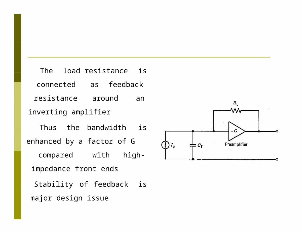
Transimpedance front end provides high
sensitivity together with large bandwidth
Its dynamic range is also improved compared
with high-impedance front end
These are often used in optical receivers
because of their improved characteristics
as
The load resistance is
connected feedback
resistance around an
inverting amplifier
Thus the bandwidth is
enhanced by a factor of G
compared with high-
impedance front ends
Stability of feedback is
major design issue

Linear ChannelLinear channel in optical receivers consists of high-gain
amp and low pass filter.
An equalizer is sometimes added to just before the
amplifier to correct for the limited bandwidth of the
front end
It has AGC to limit the average output voltage to a
fixed level irrespective of the incident average optical
power at the receiver
The low pass filter shapes the voltage pulse and
reduces noise without intersymbol interference (ISI).
The low pass filter has the smallest bandwidth so the

The combination of preamplifier, main amplifier, and thefilter acts as a linear system hence given the name linearchannel
Equalizer Ip(t)Preamp Amp
Filter
Zin(ω) Gp(ω) GA(ω) HF(ω)
ZT(ω)
Vout(t)

% I
% %
The output voltage can be written as∞
Vout t zT t Ip t ∫zT t −t 'Ip t 'dt ' -------(i)−∞
Where Ip t is the photocurrent generated in response
to the incident optical power (Ip RPin )
In freq domain Vout (ω) = ZT (ω) ⋅ %p (ω) ---------(ii)
Vout (ω) = Vin ω) ⋅ G p (ω) ⋅ G A (ω) ⋅ H F (ω)
Where ZT is the total impedance at the frequency ωand tilde represents the Fourier transform

~ ~~
~~
~
ZT (ω ) = ~
Viin ω ) = Ziin ω ) ⋅ I p ω ) =I p ωYin ω
Where Yin ωis the input admittance
Vout (ω ) =I p (ω)
Yin (ω)⋅G p (ω ) ⋅ GA (ω ) ⋅ H F (ω )
Where G p (ω), GA (ω) and H F () are transfer functions
of the preamplifier, the main amplifier and the filter
Vout (ω ) G p (ω ) ⋅ GA (ω ) ⋅ H F (ω )
I p (ω ) Yin (ω )- - - - - - - -(iii)
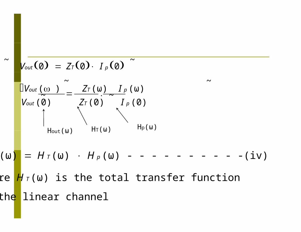
~ ~
~ ~ ⋅~~
Vout 0ZT 0⋅I p 0
Vout (ω) ZT (ω) I p (ω)
Vout (0) ZT (0) I p (0)
Hout(ω) HT(ω) Hp(ω)
H out (ω) H T (ω) ⋅H p (ω) - - - - - - - - - -(iv)
Where H T (ω) is the total transfer function
of the linear channel

Data RecoveryThe data-recovery section of optical receivers consists
of a decision circuit and a clock-recovery circuit
The purpose of clock-recovery circuit is to isolate aspectral component at f=B from the received signal
This component provides information about the bit slot
TB1B to the decision circuit and helps to synchronize
the decision process
Clock recovery is more difficult in the case of NRZformat because the signal received lacks a spectralcomponent at f=B (In RZ format a spectral componentat f=B is present)

The decision circuit compares the output from the linear
channel to threshold level, at sampling times determined by
the clock-recovery circuit and decides whether the signal
corresponds to to bit 1 or bit 0
Eye diagram is formed by superposing 2-3 bit-long
electrical sequences in the bit stream on top of each other.
It is called because of its appearance
Noise and the timing jitter causes closing of the eye. The
best sampling time corresponds to maximum opening of
the eye. Eye diagram provides a visual way of monitoring
the receiver performance

⎬data
B1
B2
Input data
Clockrecovering
input f
Decisioncircuit
Clock, f=B
RZ format,
NRZ- format
Regenerate d ⎫
Re −timed ⎭
Bit slot T B
component at f=B presentSAW filterno component at f=B

Circuit Input
Ref DFFData out
Decision comparatorclock
Eye diagramSuperimposing in same time slot
Ideal Eye diagram for NRZ format

•
•
•
Degraded Eye diagram for NRZ format
Noise and time jitter close the eye
Best sampling time for maximum opening
BER related to eye closure