optical and structural investigatio n on ingan/gan
TRANSCRIPT
Optical and structural investigation on InGaN/GaN multiple quantum well light-emitting diodes grown on sapphire by metalorganic
chemical vapor deposition Z. C. Fenga,*, J. Chena, H. Tsaib, J. Yangb, P. Lic, C. Wetzelc, T. Detchprohmc, J. Nelsonc, and I. T. Fergusond
a Graduate Institute of Electro-Optical Engineering and Department of Electrical Engineering, National Taiwan University, Taipei, Taiwan 106, ROC;
b Department of Materials Science and Engineering, National Taiwan University, Taipei, Taiwan 106, ROC; c Uniroyal Optoelectronics, Tampa, FL 33619, USA;
d School of Electrical Engineering, Georgia Institute of Technology, Atlanta, GA 30332-0250, USA * Corresponding author. E-mail: [email protected]
ABSTRACT InGaN/GaN multiple quantum well (MQW) light emitting diode (LED) structures with blue and green light emissions have been grown on sapphire substrates by metalorganic chemical vapor deposition. They are investigated by high-resolution X-ray diffraction (HR-XRD), high-resolution transmission electron microscopy (HR-TEM), photoluminescence (PL) and photoluminescence excitation (PLE). HR-XRD showed multiple satellite peaks up to 10th order due to the quantum well superlattice confinement effects. HR-TEM determined the MQW structures and parameters, indicating the high quality of layer interfaces of these LED samples. Excitation power-dependent PL predicates that both piezoelectric field-induced quantum-confined Stark effect and band filling effect influence the luminescent properties. Temperature-dependent PL shows that the QW PL emission peak exhibits a monotonic red-shift and that the full width at half maximum of the PL band shows a W-shaped temperature-dependent behavior with increasing temperature. From the PLE results, a large energy difference, so-called quantum confined Stokes shift, between the band-edge absorption and emission was observed. Penetrating TEM revealed the V-shape defects, and quantum dot-like structures within the InGaN well region, which leads to intense light emissions from these MQW LEDs.
Keywords: metalorganic chemical vapor deposition, InGaN/GaN, multiple quantum well, light emitting diode, X-ray diffraction, transmission electron microscopy, photoluminescence, photoluminescence excitation
1. INTRODUCTION
Research and developments on GaN-based compound semiconductors and structures for optoelectronic and electronic applications have been carrying out in recent years. GaN and related III-nitride semiconductors possess large direct band gaps, extremely high hardness, very large heterojunction offsets, high thermal conductivity and high melting temperature. A great deal of breakthroughs have been achieved in recent years for their materials growth and device manufactures in applications in blue-UV and visible light emitting diode (LED), laser diode (LD) and other optoelectronic and electronic devices [1–7]. InGaN-based LED and LD grown on sapphire are now available commercially. InGaN/GaN multiple quantum wells are the key components of these commercial devices emitting green, blue, near-UV, and white light, acting as the active layer in above high brightness III-nitride LED and cw blue-green laser diode LD [1,8,9]. InGaN/GaN heterostructures can exhibit intense photoluminescence (PL) and electroluminescence (EL) despite of a high dislocation and defects density existed [10,11], and have advantages such as lowering the threshold current density for LDs and reducing the device sensitivity to temperature [12,13]. However, despite an impressive commercial success, the physical origin of efficient light generation in this partially disordered system is unveiled incompletely, and there are still a lot of puzzling phenomena whose origin has yet to be explored, which is very important, not only from the viewpoint of physical interest but also in designing practical device.
In this paper, we will study the key issues of InGaN MQW LED structures, prepared by the metalorganic chemical
Sixth International Conference on Solid State Lightingedited by Ian T. Ferguson, Nadarajah Narendran, Tsunemasa Taguchi, Ian E. AshdownProc. of SPIE Vol. 6337, 63370D, (2006) · 0277-786X/06/$15 · doi: 10.1117/12.677653
Proc. of SPIE Vol. 6337 63370D-1
Downloaded From: http://proceedings.spiedigitallibrary.org/ on 11/19/2014 Terms of Use: http://spiedl.org/terms

'I
vapor deposition (MOCVD) technique, including their optical properties, photon emission mechanisms, and structural properties. We focus on two InGaN/GaN MQW LED structures on sapphire; one is designed for blue LED and the other is for green LED. Analytical techniques of photoluminescence (PL), photoluminescence excitation (PLE), high-resolution (HR) X-ray diffraction (XRD) and transmission electron microscopy (TEM) have been employed to investigate their optical and structural properties.
2. Experiment
High quality InGaN/GaN MQW LEDs were grown on (0001)-plane (c-face) sapphire substrate by low pressure (LP) MOCVD using an Emcore system with the vertical growth configuration and a high speed rotation disk, i.e. the so-called Turbo-disc technology. Trimethylgallium (TMGa), Trimethylindium (TMIn), and ammonia NH3 were used as precursors for Ga, In, and N, respectively. The carrier gas was H2 and N2, respectively, for the growth of GaN and InGaN. For the growth procedures, the substrates are initially treated in H2 ambient at 1173oC. In order to relieve the lattice mismatch strain between GaN and sapphire substrate, 30 nm thick GaN buffer layer was grown on basal c-plane sapphire substrate at 520oC prior to the growth of 2 µm thick high temperature (HT, 1020oC) grown GaN. Followed, the temperature was lowered to 800oC to grow 800 nm InGaN layer and five or eight periods of InGaN/GaN quantum wells. Different designed MQW structures lead to different color LEDs. Two MQW LED wafers were involved in this study. A blue one (G429) consists of eight-period QWs with 3-nm InGaN wells and 10-nm-thick GaN barriers, while another green one (G978) has five-period QWs with 4-nm InGaN wells and 40-nm-thick GaN barriers. Afterwards, 50 nm p-type AlGaN and 150 nm GaN cap layer were grown at high temperature. The average indium concentration in the well is about 15% and 18 %, respectively, and all the layers are undoped.
The specimens for TEM observation were mechanically polished into a wedge shape using a Tripod polisher, followed by Ar+ ion milled at 5.0 kV to electron transparency in a Gatan Model 691 precision ion polishing system (PIPS). The prepared TEM specimen was examined using a Philips Tecnai F30 field-emission-gun electron microscope, equipped with a dark-field annular detector, operated at 300kV.
HR-XRD analysis determines the indium composition and structural parameters of these LED. Excitation-power dependent PL and temperature-dependent PL, and PLE experiments were performed to investigate their optical characteristics. Their temperature and excitation power dependence of the optical behaviors including PL line shapes and the internal quantum efficiencies showed the distinct features. The recombination mechanisms were revealed and discussed based on the theory of the quantum confined Stark effect and carrier localization effect. This result should be emphasized in designing InGaN/GaN based devices.
3. Basic Structural Results
3.1. Transmission electron microcopy image
(a) G429 (b) G978
Figure 1. HR-TEM cross section images of two InGaN/GaN MQWs.
Proc. of SPIE Vol. 6337 63370D-2
Downloaded From: http://proceedings.spiedigitallibrary.org/ on 11/19/2014 Terms of Use: http://spiedl.org/terms

Inte
nsity
(cou
nts/
s)
- -
C
- -
C
C -
o K
(a) G429 (b) G978
Figure 2. High-angle annular dark field (HAADF) STEM images of capped InGaN/GaN MQWs, simulated from Fig. 1.
Figure 1 shows high resolution (HR) transmission electron microcopy (TEM) cross section images of two MQWs. The measurements were performed with an acceleration voltage of 200 kV. All high-resolution micrographs were taken at Scherzer defocus, performed under short times of irradiation to prevent electron beam-induced artifacts [14]. Figure 2 exhibits their cross-sectional low magnified high-angle annular dark field (HAADF) STEM images of capped MQW InGaN/GaN, simulated from the original pictures of Fig. 1 by computer. HAADF STEM contrast is mainly due to thermal diffuse scattering, whose intensity is almost proportional to the square of atomic number. Bright stripes parallel to the basal plane are InGaN layers and dark ones are GaN layers. Eight and five QW structures can be clearly identified from the cross-sectional HR-TEM observation. The dark contrast clearly shows that the QW is not uniform. The well and barrier widths were determined to be 3/10 nm for sample G429 in (a) and 4/40 nm for G978 in (b), which are in good agreement with the XRD measurements and simulation results, described below.
3.2. High resolution X-ray diffraction
Figure 3 is the HR-XRD ω-2θ scans for the (0002) reflection from the 5-QW sample (G978) measured by a Philips MRD system. High order satellites up to 11th can be clearly distinguished, showing very good InGaN/GaN interfaces. The GaN peak localized at the angle of 34.56° is very sharp and all satellite bands are narrow. More fine structures are seen between satellite peaks. These indicate the excellent layer crystalline perfection and sharp interfaces between all multiple layers. Well/barrier width and average indium composition were estimated to be around 4/40 nm and 18% by using Philips X’pert Epitaxy and Smoothfit Program.
Figure 3. HRXRD ω-2θ (0002) scans for a 5-QW InGaN/GaN green LED wafer. The lower curve is the simulation result.
50 nm10 nm
HAADF D
Proc. of SPIE Vol. 6337 63370D-3
Downloaded From: http://proceedings.spiedigitallibrary.org/ on 11/19/2014 Terms of Use: http://spiedl.org/terms

4. Optical Luminescence Results
4.1. Temperature (T)-dependent photoluminescence of InGaN/GaN blue LED
2.4 2.6 2.8 3.0 3.2 3.4
PL
Inte
nsity
(a.u
.)
Energy (eV)
G429 T= 9K 15K 20K 30K 40K 50K 70K 90K110K140K170K200K250K300K
2.5 3.0 3.5
P3
P2 T= 9K 15K 20K 30K 40K 50K 70K 90K110K140K170K200K250K300K
PL
Inte
nsity
(a.u
.)
Energy (eV)
G429574meV
P1
(a) (b)
Figure 4. (a) Temperature dependent PL spectra for the InGaN/GaN 8-QWs structure from 9 to 300 K and (b) the corresponding modulated PL spectra.
Figure 4 (a) shows the experiment temperature (T)-dependent PL spectra of the 8-QWs sample in the range from 9 K to room temperature (RT). Multiple fine structures were observed due to Fabry-Perot interference fringes (thickness effect) as previously reported results [15]. This confirms that the sample (G429) has a very smooth surface. In order to see the peaks clearly, attempts were made to remove the thickness fringes by dividing the spectra by an interference function calculated using a model for the propagation of light generated in an active layer sandwiched by two heterostructures [16]. For these calculations the refractive indices were obtained from [17] (and adjusted to the temperature of measurement), and the InGaN absorption coefficient, α(E), was represented by the sigmoidal function described in [18]. The linear dependencies of the effective energy gap and absorption edge broadening on the emission energy [18] enable an estimation of α(E) for the quantum well material in this sample. The interference function is mainly dependent on the overall thickness of III-N material, which is estimated using ex situ reflectometry and cross-sectional scanning electron microscopy. However, this method is too complicated to achieve, so we use more simple way to remove the fringes carefully by the smoothing function of the Origin program.
Figure 4 (b) gives the modulated PL spectra for the 8-QWs blue sample in the temperature range from 9 to 300 K. In each case, the excitation power was fixed at ~23 mW. At the low temperature of 9 K, two InGaN-related emission peaks are clearly seen at about 2.63 eV (blue) and 3.2 (UV), which were labeled P1 and P2, respectively. The blue InGaN-related peak (P1) shows a very bright blue light emission even at 300 K, and the luminescence intensity of the P1 emission is reduced by only a factor of ~2.2, more less than one order of magnitude, with increasing temperature from 9 to 300 K, indicating high quantum efficiency and good device performance of this InGaN/GaN MQW structure. On the other hand, the luminescence intensity from the InGaN-related UV emission peak (P2) is rapidly quenched from 15 to 70 K. At the temperature of 70 K, another emission peak (P3) was observed clearly along with the emission peak P2. By increasing temperature above 90 K, the emission peak P2 is reduced quickly and exists only as a shoulder. As the temperature is further increased to 300 K, the two emission band P2 and P3 disappear and only P1 emission exists at room temperature.
As the temperature increases, the peak P2 and P3 show monotonous red-shift clearly. However, the peak P1 red-shifts slightly toward the lower energy side up to 50 K, and then blue-shifts to higher energy side with increasing the temperature. The anomalous temperature dependence of emission shift is rarely seen in literatures. This conforms that the three peaks correspond to different luminescence centers or different recombination mechanisms. The red-shift trend of the two high-energy peaks (P2 and P3) is mainly due to the band gap shrinkage with increasing temperature. It is believed that P2 and P3 emissions were the MQW-related emissions. The red-blue-shift behavior of the low-energy peak P1 was explained by the localized character of the radiative electron-hole recombination. The excitons are trapped at small potential minima and gradually increase energy with temperature. The blue-shift behavior which occurs up to
Proc. of SPIE Vol. 6337 63370D-4
Downloaded From: http://proceedings.spiedigitallibrary.org/ on 11/19/2014 Terms of Use: http://spiedl.org/terms
300 K suggests that excitons localization plays an important role for this sample even at RT. The temperature quenching of the PL is much slower for the P1 emission as compared to the P2 and P3 emissions. Both trends point towards the P1 emission peak as originating from the localization states [19].
In order to obtain blue emission (2.667 eV) at room temperature from this sample, the required indium mole fraction in the quantum well structures is about 0.31. The calculation assumes the screening effect of photo-generated carriers is negligible. The In composition obtained from PL analysis is quite high compared to that in XRD analysis (In of 18 %). The reasons is that the blue PL emission comes from the In-rich region rather than ordinary layer, which provided efficient radiative recombination pathway even at room temperature, but XRD analysis showed an average approximate In composition in the well layers.
4.2. Excitation-power-dependent Photoluminescence of blue LED wafer
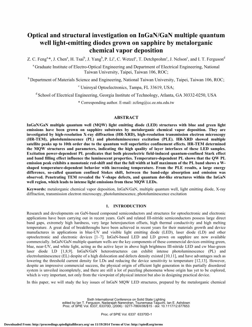
To get further evidence for the origin of these peaks, the low-temperature PL spectra of this sample with various excitation powers are shown in Figure 5. The excitation power density was changed over 200 times (from 0.14 to 31 mW). Under a low excitation power of 0.14 mW, two peaks (P1 and P3) can be observed at 2.63 and 3.01 eV, respectively. With increasing excitation power from 0.14 mW to 1.86 mW, the emission wavelength of P3 shifts to shorter wavelength (blue-shift). At the excitation power of 3.77 mW, another peak P2 was observed clearly along with P1 and P3 emissions. With increasing excitation power from 3.77 to 31 mW, the peak P2 becomes dominant and also shifts to much shorter wavelength (blue-shift). In addition, the emission energy of peak P1 is almost independent of the excitation power density, which is typical of excitionic transition [20]. It also indicates that the neglection of photo-carriers screening effect in the calculation is reasonable. The peak P2 and P3 show a clear blue-shift with increasing the excitation power density. There are two possible explanations for the blue-shift behavior. One refers to the field-induced QCSE, and another is related to the band-filling effect.
Fig. 3.5 Low temperature PL spectra of the InGaN/GaN 8QWs structure measure with different excitation intensities. All spectra are normalized and shifted vertically for clarity.
4.3. Temperature (T)-dependent Photoluminescence of InGaN/GaN Green LED wafer
Figure 6 shows the T-dependent PL spectra for the InGaN/GaN green LED sample from 9 to 300 K. In each case, the excitation power was fixed at ~20 mW. Different from previous blue LED MQW sample, single peak emission was observed over all temperatures, and the decrease of peak intensity is slow with an increase in temperature. The PL peak positions of QW-related band for this sample exhibit a monotonous red-shift. In general, with increasing temperature the band gap shrinks due to the temperature-dependent dilation of the lattice [21] and electron–lattice interaction. Thus, the peak position of PL spectrum exhibits only the red-shift. The empirical equation for this characteristic has been given by the Varshni formula [22], E(T)= E(0)-αT2/ (T+β), where E(T) denotes the energy gap at the temperature of T K; E(0) at 0 K, and α and β constants. The constants α and β are considered in principle dependent on the sample compositions, but independent of the growth method and the well width [23]. Assuming the In composition in the well layers of all samples being same, we used the same values of the constants α and β to all samples. The values of α and β were evaluated from the linear interpolation from the values for GaN and InN. The indium fraction is 18 % determined by XRD measurement. The energy gap E(T) variations of In0.18Ga0.82N with temperature are shown together with the experimental data in Figure 7 (a). The values of α and β are 0.77 meV/K and 600 K for GaN [24] and 0.245 meV/K and 624 K for InN [25], respectively.
The deviation of the PL peak position from the Varshni’s characteristics is considered due to the thermal broadening of carrier distribution, the delocalization of carriers, the dissociation of the excitons, and the piezoelectric field intensity with temperature change [23]. The points in Fig. 7 (b) show a W-shaped temperature dependence of the full width at
2.4 2.6 2.8 3.0 3.2 3.4 3.6
P3
P2
0.142mW
0.27mW
0.52mW
0.97mW
1.86mW
3.77mW
6.71mW
12.1mW
20.9mW
31.0mW
PL
Inte
nsity
(a.u
.)
Energy (eV)
Ex-power :
G429
P1
Proc. of SPIE Vol. 6337 63370D-5
Downloaded From: http://proceedings.spiedigitallibrary.org/ on 11/19/2014 Terms of Use: http://spiedl.org/terms

experimental data
ln01Ga081.
FiN2.38
$ 2.372.36
1 2.35 -
2.34 -
a233232 -
D-2.31-2.30 GaN2.29H1....1....1....1 I
0.18- -
O.17- -> •.—•s016_ .—-—- -• .•.
0.15- -
LI- 0.14- -
0.13 -(br--•-— -
0 50 100 ISO 200 250 300Temperature (K)
half maximum (FWHM) with a characteristic kink at about 140 K. The W-shaped temperature behavior of the linewidth is known to be a signature of excitons hopping over randomly dispersed localized states with a crossover from a nonthermalized to a thermalized distribution function of the excitons.
2.0 2.1 2.2 2.3 2.4 2.5 2.6
G978i
PL
Inte
nsity
(a.u
.)
Energy (eV)
T= 9K 15K 30K 40K 50K 70K 90K110K140K170K200K250K300K
Figure 6. The PL spectra for the InGaN/GaN 5-QWs green LED structure in the temperature range from 9 to 300 K.
Figure 7. Temperature dependence of the peak position (a) and the FWHM (b) for the InGaN/GaN 5-QWs green LED structure.
Figure 8 shows the temperature dependence of the normalized integrated PL intensity in Arrhenius plot for the InGaN/GaN 5-QWs green LED structure. The integrated PL intensity falls gradually with increasing temperature due to increasing nonradiative recombination path. Assuming that the internal quantum efficiency (ηint) equals unity at 9 K, we obtain ηint of 0.29 at room temperature. Furthermore, it appears that the data cannot be well fitted by an Arrhenius formula: I(T)=I0/[1+αexp(-EA/kBT)]. Instead, the relationship is similar to that used for amorphous semiconductors and disordered superlattices [26]: I(T)=I0/[1+Aexp(T/T0)], where I(T) is the PL intensity at the temperature T, T0 the characteristic temperature corresponding to the energy depth of localized states from a mobility edge. A is the tunneling factor and I0 is the luminescence intensity at the low-temperature limit. The latter equation is valid if localized band-tail states exist [27]. Therefore, it seems reasonable to infer that the PL signal in the InGaN QWs comes from localized states.
Figure 8. Temperature dependence of the normalized integrated PL intensity for the InGaN/GaN green LED structure.
4.4. Excitation-power-dependent Photoluminescence of InGaN/GaN Green LED wafer
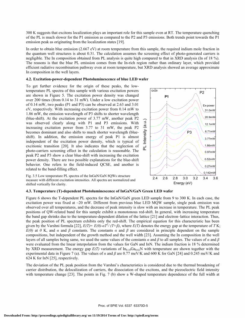
To further investigate the luminescence mechanism, the excitation power-dependent PL measurement was carried out. Figure 9 describes the excitation power dependence of PL spectra of the 5-QWs green LED sample. With increasing the excitation power from 0.07 to 33.1 mW, the emission shows a clear blue-shift. Figure 10 shows the excitation power dependence of the emission peak energy in (a) and the full width at half maximum (FWHM) in (b) of the main emission, respectively. A blue-shift of ~163 meV for the QW peak is evident in Fig. 10 (a) as the excitation power increases from 0.07 mW to 33.1 mW. For the blue-shift of emission energy in this sample, normally, there are two possible explanations. One refers to the piezoelectric field-induced QCSE [28], and another is related to the band-filling effect at the self-organized small In-rich regions [29]. In addition, in Fig. 10 (b) the FWHM of the emission peak decreases with increasing excitation power from 0.07 to 3.2 mW, and then increases with increasing excitation power up to 33.1 mW. Such anomalous excitation power dependence of the emission linewidth behavior is rarely seen in literatures, but monotonous increasing or decreasing phenomena of the emission peak linewidth for InGaN/GaN QW structure were observed by another group [30]. Our results can be well explained in the terms of the QCSE along with the state filling
0 20 40 60 80 100 1200.2
0.3
0.4
0.5
0.60.70.80.9
11.1
170K
300K
250K
200K
40K30K 15K
1000/T (K-1)
N
orm
aliz
ed In
tegr
ated
PL
Inte
nsity
9K
Proc. of SPIE Vol. 6337 63370D-6
Downloaded From: http://proceedings.spiedigitallibrary.org/ on 11/19/2014 Terms of Use: http://spiedl.org/terms
FW
HM
(eV
) P
eak
posi
tion
(eV
)
9 9
9 9
9 9
o o
- a
Foa
o,oJ
ao,o
N N
N
effect. Due to the lattice mismatch between InGaN and GaN, the InGaN wells were under biaxial stress. In such a case, a piezoelectric field is induced since group III nitrides have large piezoelectric constants along the [0001] orientation [31]. Therefore, the optical properties are strongly affected by this piezoelectric field, which produces QCSE. Due to the QCSE, the emission peak will show a red-shift and the peak linewidth will be broadened, which has been observed earlier in the GaAs system [32]. The piezoelectric field can be screened by photo-generated carriers. The increase of the excitation power from 0.07 to 3.2 mW weakens the QCSE and thus increases the transition energy, resulting in a blueshift, and decreases the FWHM of the peak at the same time. At higher excitation power more than 3.2 mW, the piezoelectric field seems to be fully screened, which the linewidth doesn’t decrease any more. Then, the band-filling were the dominant effect, which can cause the emission energy blue-shift also. On the other hand, the band filling can explain the broadening of the emission linewidth. At high level excitation, radiative recombination from high higher energy states will occur because there are more injected carriers and the possibility of higher energy states being filled with the excited carriers is larger. Most of these excited carriers at the higher energy states relax to the ground states and the ground state recombinations still dominate the PL emission, while only a small amount can directly recombine and emit light of larger energy. It can cause the PL emission blueshift and broader as the excitation power is further increased.
2 .0 2 .1 2 .2 2 .3 2 .4 2 .5 2 .6
E x-P o w e r : (m W )
0 .0 70 .3 6
0 .7 61 .5 8
3 .2
8 .4
1 3 .6
2 3 .8
3 3 .1
PL In
tens
ity (a
.u.)
E n e rg y (e V )
G 9 78
Figure 9. Low temperature PL spectra of the InGaN/GaN green LED under different excitation intensities. All spectra are normalized and shifted vertically for clarity.
Figure 10. Excitation power dependence of the peak position (a) and the FWHM (b) for the InGaN/GaN 5-QWs green LED structure.
4.5. Photoluminescence Excitation of blue and green LEDs
2.0 2.2 2.4 2.6 2.8 3.0 3.2 3.4 3.6 3.8
PLE
G429
Energy (eV)
PL
1.5 2.0 2.5 3.0 3.5
Gaussian curve
Energy (eV)
PL
Inte
nsity
(a.u
.) PLE
PL2nd
1P
LE In
tens
ity (a
.u.)
(a) blue LED (b) green LED
Figure 11. PLE spectra at room temperature for the InGaN/GaN MQW blue and green LED structures.
Proc. of SPIE Vol. 6337 63370D-7
Downloaded From: http://proceedings.spiedigitallibrary.org/ on 11/19/2014 Terms of Use: http://spiedl.org/terms
[0001]
[1010] -[1210]
I I2OnnlH
11.
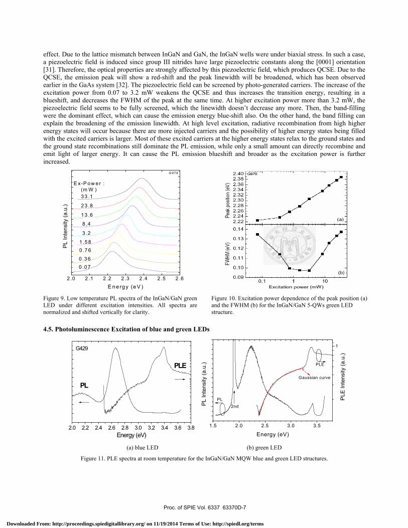
Figure 11 shows PL and PLE spectra of two InGaN/GaN MQW blue and green LED structures at room temperature. In both cases, the most efficient excitation of the QW luminescence is achieved via the GaN barriers at energies above 3.5 eV, due to the fact that at most a few percent of the exciting light is directly absorbed in the quantum well. The high quality of the GaN layers can be inferred from the narrow excitonic absorption peak at the GaN absorption edge. To be different in these cases, the blue LED sample seems to have two absorption edges, while the green one has only one absorption edge below the GaN absorption peak. The absorption band edges correspond to InGaN QW emission for the two samples show distinct distribution. We fit these PLE data by Gaussian function [33]: exp[-(E-E0)2/ 2σ2], where σ is the broadening parameter of the Gaussian. The broadening parameter σ of the green LED is calculated to be 806.5 meV, which is also ~1.8 times larger than that of blue LED. Correspondingly, the PL linewidth of the green LED (430 meV) is ~1.7 times larger than blue LED (260 meV). This is because the green LED has higher degree of indium fluctuations than blue LED. As a result, the explicit character of disorder in particular cases strongly depends on the growth conditions used. This suggests that the indium fluctuation and carrier localization strongly depends on the growth conditions of InGaN active layers.
5. Discussion – V-defects and quantum dots like structure
5.1. Transmission electron microcopy image on V-defects
(a) (b)
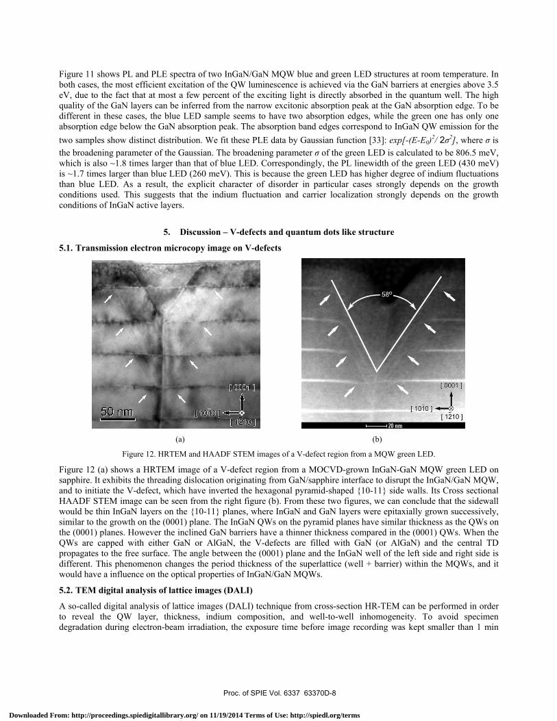
Figure 12. HRTEM and HAADF STEM images of a V-defect region from a MQW green LED.
Figure 12 (a) shows a HRTEM image of a V-defect region from a MOCVD-grown InGaN-GaN MQW green LED on sapphire. It exhibits the threading dislocation originating from GaN/sapphire interface to disrupt the InGaN/GaN MQW, and to initiate the V-defect, which have inverted the hexagonal pyramid-shaped {10-11} side walls. Its Cross sectional HAADF STEM image can be seen from the right figure (b). From these two figures, we can conclude that the sidewall would be thin InGaN layers on the {10-11} planes, where InGaN and GaN layers were epitaxially grown successively, similar to the growth on the (0001) plane. The InGaN QWs on the pyramid planes have similar thickness as the QWs on the (0001) planes. However the inclined GaN barriers have a thinner thickness compared in the (0001) QWs. When the QWs are capped with either GaN or AlGaN, the V-defects are filled with GaN (or AlGaN) and the central TD propagates to the free surface. The angle between the (0001) plane and the InGaN well of the left side and right side is different. This phenomenon changes the period thickness of the superlattice (well + barrier) within the MQWs, and it would have a influence on the optical properties of InGaN/GaN MQWs.
5.2. TEM digital analysis of lattice images (DALI)
A so-called digital analysis of lattice images (DALI) technique from cross-section HR-TEM can be performed in order to reveal the QW layer, thickness, indium composition, and well-to-well inhomogeneity. To avoid specimen degradation during electron-beam irradiation, the exposure time before image recording was kept smaller than 1 min
Proc. of SPIE Vol. 6337 63370D-8
Downloaded From: http://proceedings.spiedigitallibrary.org/ on 11/19/2014 Terms of Use: http://spiedl.org/terms

[34]. Figure 13 provides such TEM DALI images of the studied green LED, showing the color-coded map of the local In concentration in this InGaN/GaN MQW structure containing 5 InGaN well layers. The left pattern is from QW1 just next to the capping layer and the right one is from QW5 at the bottom of the active layer. The quantum dot (QD)-like structures around the In-rich areas are formed [35], which is the cause of strong luminescence from InGaN/GaN MQWs.
(a) QW1 (b) QW5
Figure 13. HR-TEM DALI images of the green LED, showing the color-coded map of the local In concentration with the left one from QW1 just next to the capping layer and the right one from QW5 at the bottom of the active layer.
6. Conclusion
In conclusion, we have studied the optical and structural properties of the InGaN/GaN MQW blue and green LED samples. From HR-XRD analysis, we can determine the period thickness and indium composition of our samples. Different temperature-dependent PL and excitation-power dependence of PL behaviors were studied between the two blue and green LED samples. For the blue LED, blue and UV emissions can be observed at low temperature. With increasing temperature, the UV emission was rapidly quenched. But the blue emission remained bright at room temperature. We expected that the blue and UV emission correspond to different luminescence centers or different recombination mechanisms. The blue emission also showed a red-blue shift with variation of the temperature due to carrier localization in the potential minima caused by inhomogeneous alloy distribution in the well. Excitation power dependent PL experiment was also performed to prove our assumptions. For the green LED, HR-XRD showed multiple satellite peaks up to 11th order due to the quantum well superlattice confinement effects. These indicate the high quality of layer interface structures for this sample. The peak position of the emission exhibits a monotonic red-shift and the FWHM show a W-shaped variation with increasing temperature. The temperature quenching behavior does not fit in with Arrhenius formula but is similar to the behavior of amorphous semiconductors. By comparing these two blue and green LED samples with similar structures but different parameters, the PLE spectra show different features. From excitation power dependent PL results, we can expect that band-filling and QCSE both play an important role in the recombination process. We can believe that different emission mechanisms occur between our blue and green LED.
Penetrating HR-TEM investigation reveal the existence of V-shape defects, which can be observed in high quality MQW LED samples only. They were initiated due to the threading dislocation originating from GaN/sapphire interface, developed to disrupt the InGaN/GaN MQW, and have inverted the hexagonal pyramid-shaped {10-11} side walls. A so-called digital analysis of lattice images (DALI) technique from cross-section HR-TEM has been performed and the inhomogeneities of the QW layer, thickness, indium composition, and well-to-well are clearly revealed. The color-coded maps of the local In concentration within the InGaN/GaN MQW structure are obtained and the quantum dot (QD)-like structures around the In-rich areas are found to form within the InGaN well layers, which is the cause of strong luminescence from InGaN/GaN MQWs.
Our results can be explained by alloy potential fluctuations in a consistent way. We may suggest that the compositional fluctuations do exist and lead to the formation of QDs-like structures to enhance the major luminescence in our InGaN
Proc. of SPIE Vol. 6337 63370D-9
Downloaded From: http://proceedings.spiedigitallibrary.org/ on 11/19/2014 Terms of Use: http://spiedl.org/terms

MQW LED wafers. It also suggests that the indium fluctuation and carrier localization strongly depends on the growth conditions of InGaN active layers.
REFERENCES 1. S. Nakamura, S. Pearton, G. Fasol, The Blue Laser Diode—The Complete Story, Springer, Berlin, 2000. 2. J.I. Pankove, T.D. Moustakas ed., Gallium Nitride (GaN) I and II, Semiconductors and Semimetals, ed. R.K.Willardson and
E.R. Weber, Vol. 50 and 58, Academic, San Diego, 1998 and 1999. 3. H. Morkoc, Nitride Semiconductors and Devices, Springer, Berlin, 1999. 4. S. Nakamura, S.G. Chichibu (Eds.), Introduction to Nitride Semiconductor Blue Lasers and Light Emitting Diodes, Taylor and
Francis, London, 2000. 5. E.T. Yu, M.O. Manasreh ed., III–V Nitride Semiconductors: Applications and Devices, Vol. 16 in M.O. Manasreh ed.,
Optoelectronic Properties of Semiconductors and Superlattices, Taylor and Francis, New York, 2003. 6. M.O. Manasreh, I.T. Ferguson ed., III –V Nitride Semiconductors: Growth, Vol. 19 in M.O. Manasreh ed., Optoelectronic
Properties of Semiconductors and Superlattices, New York, Taylor and Francis, 2003. 7. Zhe Chuan Feng, ed., GaN-Based Materials: Growth and Characterization, Imperial College Press, London, 2006. 8. S. Nakamura, M. Senoh, S. Nagahama, N. Iwasa, T. Yamada, T. Matsushita, H. Kiyoku, Y. Sugimoto, T. Kozaki, H. Umemoto,
M. Sano, K. Chocho, Appl. Phys. Lett. 72 (1998) 2014. 9. J.J. Song, W. Shan, in: B. Gil (Ed.), Gallium Nitride and Related Semiconductors, Michael Faraday House, 1998, p. 596. 10. Nakamura, S., Senoh, M., Nagahama, S., Iwasa, N., Yamada, T., Nukai, T., Appl. Phys. Lett., 68, 3286 (1996); 69, 1477 (1996);
69, 4056 (1996). 11. K.S. Ramaiah, Y.K. Su, S.J. Vhang, B. Kerr, H.P. Liu, L.G. Chen, Appl. Phys. Lett. 84, 3307 (2004). 12. M. Koike, S. Yamasaki, S. Nagai, N. Koide, S. Asami, H. Amano, I. Akasaki, Appl. Phys. Lett. 68, 1403 (1996). 13. H. Gotoh, T. Tawara, Y. Kobayashi, N. Kobayashi, T. Saitoh, Appl. Phys. Lett. 83, 4791 (2003). 14. T.M. Smeeton, M.J. Kappers, J.S. Barnard, M.E. Vickers, C.J. Humphreys, Appl. Phys. Lett. 83, 5419 (2003). 15. Keunjoo Kim, Jeong Yong Lee, and Sae Chae Jeoung, Thin Solid Films 478, 286 (2005). 16. Siozade L, Leymarie J, Disseix P, Vasson A, Mihailovic M, Grandjean N, Leroux M, and Massies J, Solid State Comm. 115,
575 (2000). 17. Peng T and Piprek J, Electron. Lett. 32, 2285 (1996). 18. Martin R W, Middleton P G, O’Donnell K P and Van der Stricht W, Appl. Phys. Lett. 74, 263 (1999). 19. H. C. Wang, Y. C. Lu, C. C. Teng, Y. S. Chen, C. C. Yang, K. J. Ma, C. C. Pan, and J. I. Chyi, J. Appl. Phys. 97, 033704
(2005). 20. J. Bardeen, W. Shockley, Phys. Rev. 80, 72 (1950). 21. Y.P. Varshni, Physica 34, 149 (1967). 22. A. Sasaki, K. Nishizuka, T. Wang, S. Sakai, A. Kaneta, Y. Kawakami, and Sg. Fujita, Solid State Commun. 129, 31 (2004). 23. C.F. Li, Y.S. Huang, L. Malikova, F.H. Pollak, Phys. Rev. B 55, 9251 (1997). 24. M.E. Levinshtein, S.L. Rumyantsev, M.S. Shur, Properties of Advancd Semiconductor Materials, Wiley, New York, pp. 4
(2001). 25. Street R A, Searle T M and Augustein I G 1974 Amorphous and Liquid Semiconductors ed J Stuke and W Brenig (London:
Taylor and Francis) p 953. 26. Yamamoto T, Kasu M, Noda S, and Sasaki A, J. Appl. Phys. 68, 5318 (1990). 27. Mooney P M, J. Appl. Phys. 67, R1 (1990). 28. H. Gotoh, T. Tawara, Y. Kobayashi, N. Kobayashi, T. Saitoh, Appl. Phys. Lett. 83, 4791 (2003). 29. A. Statake, Y. Masmoto, T. Miyajima, T. Asatsuma, F. Nakamura, and M. Ikeda, Phys. Rev. B 57, R2041 (1998). 30. S. Khatsevich and D. H. Rich, X. Zhang, W. Zhou, and P. D. Dapkus, J. Appl. Phys. 95, 1832 (2004). 31. T. Takeuchi, S. Sota, M. Katsuragawa, M. Komori, H. Takeuchi, H. Amano, and I. Akasaki, Jpn. J. Appl. Phys., Part 2, 36,
L382 (1997). 32. D. A. B. Miller, D. S. Chemla, T. C. Damen, A. C. Gossard, W. Wiegmann, T. H. Woodand, and C. A. Burrus, Phys. Rev. Lett.
26, 2173 (1984). 33. P. G. Eliseev, J. Appl. Phys. 93, 5404 (2003). 34. B. Witzigmann,_ V. Laino, M. Luisier, U. T. Schwarz, G. Feicht, W. Wegscheider, K. Engl, M. Furitsch, A. Leber, A. Lell, and
V. Härle, Appl. Phys. Lett. 88, 021104 (2006). 35. Y. L. Lai, C. P. Liu and Z. Q. Chen, Appl. Phys. Lett. 86, 121915 (2005).
Proc. of SPIE Vol. 6337 63370D-10
Downloaded From: http://proceedings.spiedigitallibrary.org/ on 11/19/2014 Terms of Use: http://spiedl.org/terms