operational amplifier fundamentals - labvolt series by … · exercise 3 – basic op amp...
TRANSCRIPT

Operational Amplifier Fundamentals
Student Workbook
91571-00 Edition 4 Ê>Y*èRÆ3GË
3091571000503


FOURTH EDITION
Second Printing, March 2005
Copyright February, 2003 Lab-Volt Systems, Inc.
All rights reserved. No part of this publication may be reproduced, stored in a retrieval system, or transmitted in any form by any means, electronic, mechanical, photocopied, recorded, or otherwise, without prior written permission from Lab-Volt Systems, Inc.
Information in this document is subject to change without notice and does not represent a commitment on the part of Lab-Volt Systems, Inc. The Lab-Volt F.A.C.E.T.® software and other materials described in this document are furnished under a license agreement or a nondisclosure agreement. The software may be used or copied only in accordance with the terms of the agreement.
ISBN 0-86657-208-2 Lab-Volt and F.A.C.E.T.® logos are trademarks of Lab-Volt Systems, Inc. All other trademarks are the property of their respective owners. Other trademarks and trade names may be used in this document to refer to either the entity claiming the marks and names or their products. Lab-Volt System, Inc. disclaims any proprietary interest in trademarks and trade names other than its own.

Lab-Volt License Agreement By using the software in this package, you are agreeing to become bound by the terms of this License Agreement, Limited Warranty, and Disclaimer. This License Agreement constitutes the complete agreement between you and Lab-Volt. If you do not agree to the terms of this agreement, do not use the software. Promptly return the F.A.C.E.T. Resources on Multimedia (CD-ROM) compact discs and all other materials that are part of Lab-Volt's F.A.C.E.T. product within ten days to Lab-Volt for a full refund or credit. 1. License Grant. In consideration of payment of the license fee, which is part of the price you paid for this Lab-Volt product, Lab-Volt, as Licensor, grants to you, the Licensee, a nonexclusive, nontransferable license to use this copy of the CD-ROM software with the corresponding F.A.C.E.T. Lab-Volt reserves all rights not expressly granted to the Licensee. 2. Ownership. As the Licensee, you own the physical media on which the CD-ROM is originally or subsequently recorded or fixed, but Lab-Volt retains title to and ownership of the software programs recorded on the original compact disc and any subsequent copies of the CD-ROM, regardless of the form or media in or on which the original and other copies may exist. This license is not a sale of the original software program of Lab-Volt's CD-ROM or any portion or copy of it. 3. Copy Restrictions. The CD-ROM software and the accompanying materials are copyrighted and contain proprietary information and trade secrets of Lab-Volt. Unauthorized copying of the CD-ROM even if modified, merged, or included with other software or with written materials is expressly forbidden. You may be held legally responsible for any infringement of Lab-Volt's intellectual property rights that is caused or encouraged by your failure to abide by the terms of this agreement. You may make copies of the CD-ROM solely for backup purposes provided the copyright notice is reproduced in its entirety on the backup copy. 4. Permitted Uses. This CD-ROM, Instructor's Guide, and all accompanying documentation is licensed to you, the Licensee, and may not be transferred to any third party for any length of time without the prior written consent of Lab-Volt. You may not modify, adapt, translate, reverse engineer, decompile, disassemble, or create derivative works based on the Lab-Volt product without the prior written permission of Lab-Volt. Written materials provided to you may not be modified, adapted, translated, or used to create derivative works without the prior written consent of Lab-Volt. 5. Termination. This agreement is effective until terminated. It will terminate automatically without notice from Lab-Volt if you fail to comply with any provisions contained herein. Upon termination you shall destroy the written materials, Lab-Volt's CD-ROM software, and all copies of them, in part or in whole, including modified copies, if any.
6. Registration. Lab-Volt may from time to time update the CD-ROM. Updates can be made available to you only if a properly signed registration card is filed with Lab-Volt or an authorized registration card recipient. 7. Miscellaneous. This agreement is governed by the laws of the State of New Jersey.
Limited Warranty and Disclaimer This CD-ROM software has been designed to assure correct operation when used in the manner and within the limits described in this Instructor's Guide. As a highly advanced software product, it is quite complex; thus, it is possible that if it is used in hardware configurations with characteristics other than those specified in this Instructor's Guide or in environments with nonspecified, unusual, or extensive other software products, problems may be encountered by a user. In such cases, Lab-Volt will make reasonable efforts to assist the user to properly operate the CD-ROM but without guaranteeing its proper performance in any hardware or software environment other than as described in this Instructor's Guide. This CD-ROM software is warranted to conform to the descriptions of its functions and performance as outlined in this Instructor's Guide. Upon proper notification and within a period of one year from the date of installation and/or customer acceptance, Lab-Volt, at its sole and exclusive option, will remedy any nonconformity or replace any defective compact disc free of charge. Any substantial revisions of this product, made for purposes of correcting software deficiencies within the warranty period, will be made available, also on a licensed basis, to registered owners free of charge. Warranty support for this product is limited, in all cases, to software errors. Errors caused by hardware malfunctions or the use of nonspecified hardware or other software are not covered. LICENSOR MAKES NO OTHER WARRANTIES OF ANY KIND CONCERNING THIS PRODUCT, INCLUDING WARRANTIES OR MERCHANTABILITY OR OF FITNESS FOR A PARTICULAR PURPOSE. LICENSOR DISCLAIMS ALL OBLIGATIONS AND LIABILITIES ON THE PART OF LICENSOR FOR DAMAGES, INCLUDING BUT NOT LIMITED TO SPECIAL OR CONSEQUENTIAL DAMAGES ARISING OUT OF OR IN CONNECTION WITH THE USE OF THE SOFTWARE PRODUCT LICENSED UNDER THIS AGREEMENT. Questions concerning this agreement and warranty and all requests for product repairs should be directed to the Lab-Volt field representative in your area. LAB-VOLT SYSTEMS, INC. P.O. Box 686 Farmingdale, NJ 07727 Attention: Program Development Phone: (732) 938-2000 or (800) LAB-VOLT Fax: (732) 774-8573 Technical Support: (800) 522-4436 Technical Support E-Mail: [email protected]

i
THIS PAGE IS SUPPOSE TO BE BLANK Table of Contents
Unit 1 – The Operational Amplifier .............................................................................................1
Exercise 1 – Op Amp Types and Packages.................................................................................6 Exercise 2 – Op Amp Circuit Board Familiarization..................................................................8 Exercise 3 – Basic Op Amp Characteristics .............................................................................10
Unit 2 – The Inverting Amplifier................................................................................................13 Exercise 1 – Inverting Amplifier DC Operation.......................................................................16 Exercise 2 – Inverting Amplifier AC Operation.......................................................................18 Exercise 3 – Inverting Amplifier Response ..............................................................................19
Unit 3 – The Noninverting Amplifier .........................................................................................21 Exercise 1 – Noninverting Amplifier DC Operation ................................................................24 Exercise 2 – Noninverting Amplifier AC Operation ................................................................26 Exercise 3 – Noninverting Amplifier Response........................................................................27
Unit 4 – The Voltage Follower ....................................................................................................29 Exercise 1 – Voltage Follower DC Operation ..........................................................................33 Exercise 2 – Inverting Gain-of-One Amplifier .........................................................................34 Exercise 3 – Voltage Follower AC Characteristics...................................................................36
Unit 5 – The Inverting Summer..................................................................................................39 Exercise 1 – Amplifier Operation .............................................................................................43 Exercise 2 – Averaging .............................................................................................................45
Unit 6 – The Noninverting Summing Amplifier........................................................................47 Exercise 1 – Noninverting Summing Amplifier Operation ......................................................50 Exercise 2 – Summing and Averaging Operation.....................................................................51
Unit 7 – The Difference Amplifier..............................................................................................53
Exercise 1 – Difference Amplifier DC Operation.....................................................................56 Exercise 2 – Difference Amplifier AC Operation.....................................................................57
Unit 8 – Voltage Comparators ....................................................................................................59 Exercise 1 – Open-Loop Operation...........................................................................................63 Exercise 2 – Zener-Clamped Operation....................................................................................64 Exercise 3 – Square Wave Converter........................................................................................65
Appendix A – Safety ................................................................................................................. A-ii

ii
THIS
iii
Introduction
This Student Workbook provides a unit-by-unit outline of the Fault Assisted Circuits for Electronics Training (F.A.C.E.T.) curriculum. The following information is included together with space to take notes as you move through the curriculum. ♦ The unit objective ♦ Unit fundamentals ♦ A list of new terms and words for the unit ♦ Equipment required for the unit ♦ The exercise objectives ♦ Exercise discussion ♦ Exercise notes The Appendix includes safety information.

iv
THIS
Operational Amplifier Fundamentals Unit 1 – The Operational Amplifier
1
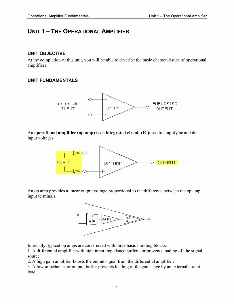
UNIT 1 – THE OPERATIONAL AMPLIFIER
UNIT OBJECTIVE At the completion of this unit, you will be able to describe the basic characteristics of operational amplifiers.
UNIT FUNDAMENTALS
An operational amplifier (op amp) is an integrated circuit (IC)used to amplify ac and dc input voltages.
An op amp provides a linear output voltage proportional to the difference between the op amp input terminals.
Internally, typical op amps are constructed with three basic building blocks. 1. A differential amplifier with high input impedance buffers, or prevents loading of, the signal source. 2. A high gain amplifier boosts the output signal from the differential amplifier. 3. A low impedance, or output, buffer prevents loading of the gain stage by an external circuit load.

Operational Amplifier Fundamentals Unit 1 – The Operational Amplifier
2
Typical op amps use several types of signal functions. Positive and negative supply terminals connect to the system power supply rails and provide operating power. Null, or nulling, terminals connect to an external voltage and allow for op amp offset voltage adjustment. Inverting (-)and noninverting (+) terminals connect to the circuit input voltages. An output terminal drives the external circuit load.
On many circuit drawings, the voltage supply terminals and the nulling terminals are not shown.
An op amp in the open loop mode has no feedback path between its output and input connections. For an ideal op amp, open-loop gain is infinite.

Operational Amplifier Fundamentals Unit 1 – The Operational Amplifier
3
If the voltages at the noninverting and inverting inputs are equal, the op amp output is saturated.
Due to the extremely high open-loop gain, a small voltage difference between the op amp inputs causes the output voltage to swing toward one of the power supply levels (voltage).
The output voltage polarity of an op amp is identical to the polarity of the voltage at the noninverting input terminal. NOTE: Typically, voltage polarity is with respect to circuit common. However, op amp inputs can be referenced to one another.
Operational Amplifier Fundamentals Unit 1 – The Operational Amplifier
4
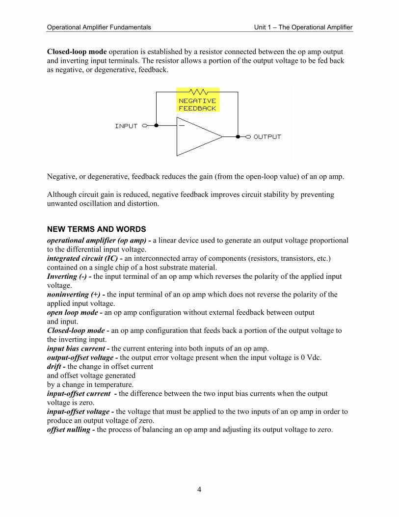
Closed-loop mode operation is established by a resistor connected between the op amp output and inverting input terminals. The resistor allows a portion of the output voltage to be fed back as negative, or degenerative, feedback.
Negative, or degenerative, feedback reduces the gain (from the open-loop value) of an op amp. Although circuit gain is reduced, negative feedback improves circuit stability by preventing unwanted oscillation and distortion.
NEW TERMS AND WORDS operational amplifier (op amp) - a linear device used to generate an output voltage proportional to the differential input voltage. integrated circuit (IC) - an interconnected array of components (resistors, transistors, etc.) contained on a single chip of a host substrate material. Inverting (-) - the input terminal of an op amp which reverses the polarity of the applied input voltage. noninverting (+) - the input terminal of an op amp which does not reverse the polarity of the applied input voltage. open loop mode - an op amp configuration without external feedback between output and input. Closed-loop mode - an op amp configuration that feeds back a portion of the output voltage to the inverting input. input bias current - the current entering into both inputs of an op amp. output-offset voltage - the output error voltage present when the input voltage is 0 Vdc. drift - the change in offset current and offset voltage generated by a change in temperature. input-offset current - the difference between the two input bias currents when the output voltage is zero. input-offset voltage - the voltage that must be applied to the two inputs of an op amp in order to produce an output voltage of zero. offset nulling - the process of balancing an op amp and adjusting its output voltage to zero.

Operational Amplifier Fundamentals Unit 1 – The Operational Amplifier
5
EQUIPMENT REQUIRED F.A.C.E.T. base unit OPERATIONAL AMPLIFIER FUNDAMENTALS circuit board Multimeter Oscilloscope, dual trace Generator, sine wave
NOTES ______________________________________________________________________________ ______________________________________________________________________________ ______________________________________________________________________________ ______________________________________________________________________________ ______________________________________________________________________________ ______________________________________________________________________________ ______________________________________________________________________________ ______________________________________________________________________________ ______________________________________________________________________________ ______________________________________________________________________________
Operational Amplifier Fundamentals Unit 1 – The Operational Amplifier
6
Exercise 1 – Op Amp Types and Packages
EXERCISE OBJECTIVE When you have completed this exercise, you will be able to recognize different op amp packages. You will verify your knowledge through observation and recognition.
EXERCISE DISCUSSION • Op amps are available in a variety of package styles. • Op amp package material can be metal, ceramic, or plastic. • Not all IC pins connect electrically to the op amp. • "No connection" (NC) pins add stability and ruggedness to the package. • From a bottom view, pin count progresses in a clockwise (CW) direction • From a top view, pin count progresses in a counterclockwise (CCW) direction. • On a TO-5 (top hat) package, pin 1 is located adjacent to the package tab. • On the flat pack, pin 1 is located adjacent to the dot or round indentation on the top side of
the package. • On the DIP package, pin 1 is located adjacent to the dot or half round notch on the top side of
the package. • ICs are available in single or multiple op amp configurations: typically one, two (dual), or
four (quad) per package. • The LF441 used on the circuit board is a single op amp package type. • The LF441 DIP outline shows the IC pin assignments. These assign-ments are set by the
device manufacturer and cannot be altered. • Since each op amp type is unique, the device manufacturer stamps a part number on the top
surface of each IC. • The TO-5 LF441 op amp outline shows the same pin assignments as the DIP, but in a
circular pattern. • Dual and quad style LF441 op amps have specific pin assignments. Note the absence of null
inputs.
Operational Amplifier Fundamentals Unit 1 – The Operational Amplifier
7
NOTES ______________________________________________________________________________ ______________________________________________________________________________ ______________________________________________________________________________ ______________________________________________________________________________ ______________________________________________________________________________ ______________________________________________________________________________ ______________________________________________________________________________ ______________________________________________________________________________ ______________________________________________________________________________ ______________________________________________________________________________

Operational Amplifier Fundamentals Unit 1 – The Operational Amplifier
8
Exercise 2 – Op Amp Circuit Board Familiarization
EXERCISE OBJECTIVE When you have completed this exercise, you will be familiar with the operation of the OPERATIONAL AMPLIFIER FUNDAMENTALS circuit board. You will verify your results by observation and measurements.
EXERCISE DISCUSSION • Three basic op amp configurations are used on your circuit board. • Only the open-loop configuration does not require a feedback path (resistor). • Inverting and non-inverting configurations generally require a feedback resistor to provide
negative feedback. • There are eight training circuit blocks on the op amp board. • Three other general purpose blocks are also required to support the training procedure. • The three general purpose blocks are labeled FOR GENERATOR BUFFER,
ATTENUATOR, and VOLTAGE DIVIDER. • The ATTENUATOR circuit block reduces an input voltage, or signal, by a factor of 10
(OUT = IN/10). • Certain procedural steps require a low-amplitude input signal. The ATTENUATOR allows
you to precisely adjust the output amplitude of a signal generator. • The VOLTAGE DIVIDER circuit block generates a variable low-voltage output between
+2.5 Vdc and -2.5 Vdc. • If a two-post connector is inserted into the circuit block, the range of output voltage is
reduced to between +0.5 Vdc and -0.5 Vdc. • The circuit block labeled FOR GENERATOR BUFFER is used with an optional generator
buffer plug-in module. This module interfaces devices without 50 output impedance to the circuits on your circuit board.

Operational Amplifier Fundamentals Unit 1 – The Operational Amplifier
9
NOTES ______________________________________________________________________________ ______________________________________________________________________________ ______________________________________________________________________________ ______________________________________________________________________________ ______________________________________________________________________________ ______________________________________________________________________________ ______________________________________________________________________________ ______________________________________________________________________________ ______________________________________________________________________________ ______________________________________________________________________________
Operational Amplifier Fundamentals Unit 1 – The Operational Amplifier
10
Exercise 3 – Basic Op Amp Characteristics
EXERCISE OBJECTIVE When you have completed this exercise, you will be familiar with fundamental op amp characteristics. You will verify your results by performing offset null adjustments.
EXERCISE DISCUSSION • Three fundamental op amp characteristics are high input impedance, high voltage gain, and
low output impedance. • Ideal op amps have infinite input impedance. Practical op amps have typical input
impedances of 1 MΩ or more. • Ideal op amps have infinite open-loop gains. Practical op amps have typical open-loop gains
of 200,000 or more. • Ideal op amps have zero output impedance. Practical op amps have typical output
impedances of 10Ω or more. • Practical op amps possess a small input current called the input bias current. • Input bias currents generate output error voltages called output-offset voltage. • Shifts in temperature change offset current, which changes offset voltage. These changes are
referred to as drift. • If the input bias current of an op amp is low, its offset voltage will be small. • If the inputs of a practical op amp are at the same potential, output voltage should be zero.
However, due to input bias current, an output- offset voltage is generated. • The effects of input bias current can be reduced significantly by the introduction of an input-
offset current or an input-offset voltage. This process is referred to as offset nulling. • Offset nulling, or op amp trim adjust, uses an adjustable external voltage to set the op amp
output to near 0V. • High gain op amps, unless properly bypassed, may oscillate. To prevent this undesirable
condition, power supply connections must exhibit low impedance characteristics. • Bypass, or decoupling, capacitors are used to ensure op amp stability.

Operational Amplifier Fundamentals Unit 1 – The Operational Amplifier
11
NOTES ______________________________________________________________________________ ______________________________________________________________________________ ______________________________________________________________________________ ______________________________________________________________________________ ______________________________________________________________________________ ______________________________________________________________________________ ______________________________________________________________________________ ______________________________________________________________________________ ______________________________________________________________________________ ______________________________________________________________________________

Operational Amplifier Fundamentals Unit 1 – The Operational Amplifier
12
Operational Amplifier Fundamentals Unit 2 – The Inverting Amplifier
13
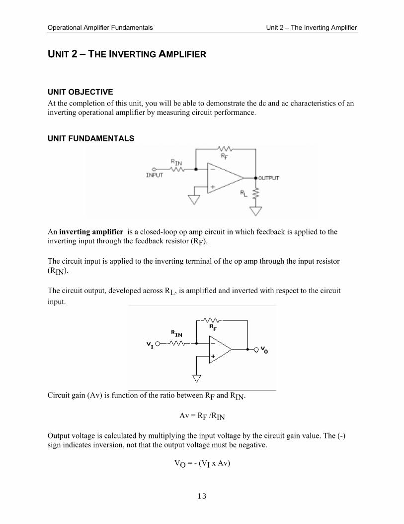
UNIT 2 – THE INVERTING AMPLIFIER
UNIT OBJECTIVE At the completion of this unit, you will be able to demonstrate the dc and ac characteristics of an inverting operational amplifier by measuring circuit performance.
UNIT FUNDAMENTALS
An inverting amplifier is a closed-loop op amp circuit in which feedback is applied to the inverting input through the feedback resistor (RF). The circuit input is applied to the inverting terminal of the op amp through the input resistor (RIN). The circuit output, developed across RL, is amplified and inverted with respect to the circuit input.
Circuit gain (Av) is function of the ratio between RF and RIN.
Av = RF /RIN Output voltage is calculated by multiplying the input voltage by the circuit gain value. The (-) sign indicates inversion, not that the output voltage must be negative.
VO = - (VI x Av)

Operational Amplifier Fundamentals Unit 2 – The Inverting Amplifier
14
Since the op amp has high gain and feedback is provided, the inverting op amp terminal is maintained at virtual ground. For this circuit configuration, the inverting op amp terminal serves as the circuit summing point.
In the circuit shown, VO represents the action of an op amp. The junction VJ is maintained at virtual ground (0V) because VO varies as VI varies. Since VJ is held at virtual ground, it is also the circuit summing junction: VJ = VI - VO. NOTE: Virtual ground and summing junction concepts will be extensively explored in this and other units.
NEW TERMS AND WORDS inverting amplifier - a circuit using an active device to amplify and invert (180-degree phase shift) an input signal. virtual ground - a circuit point that behaves like circuit common or has near zero potential with respect to circuit common. summing point - a node where two or more voltages or currents meet and algebraically combine. phase shifted - the difference between two signals; measured in units of time or degrees. Gain-bandwidth product - the product of the closed-loop gain of an op amp and its corresponding closed-loop bandwith.
Operational Amplifier Fundamentals Unit 2 – The Inverting Amplifier
15
slew rate - a measure (in volts per unit of time) of how fast a device can respond to an instantaneous change of input voltage. bandwidth - a measure of a range of frequencies that a circuit will pass without attenuation or distortion. unity-gain bandwidth - the bandwidth of an amplifier at a gain equal to one. This value is equal to the gain-bandwidth product of the op amp.
EQUIPMENT REQUIRED F.A.C.E.T. base unit OPERATIONAL AMPLIFIER FUNDAMENTALS circuit board Multimeter Oscilloscope, dual trace Generator, sine wave
NOTES ______________________________________________________________________________ ______________________________________________________________________________ ______________________________________________________________________________ ______________________________________________________________________________ ______________________________________________________________________________ ______________________________________________________________________________ ______________________________________________________________________________ ______________________________________________________________________________ ______________________________________________________________________________ ______________________________________________________________________________
Operational Amplifier Fundamentals Unit 2 – The Inverting Amplifier
16
Exercise 1 – Inverting Amplifier DC Operation
EXERCISE OBJECTIVE When you have completed this exercise, you will be able to operate an inverting amplifier. You will verify circuit operation by using a voltmeter.
EXERCISE DISCUSSION • An inverting amplifier inverts and amplifies the input voltage. • Output voltage is determined by: VO = -[VI x (RF/RIN)]. • The junction of RIN, RF, and the inverting terminal is the summing point of the circuit. • The circuit input resistance equals the value of RIN since the summing junction is at virtual
ground. • A circuit is zero-base referenced because the noninverting terminal is connected to circuit
common. • Zero-based reference circuits change their output voltage polarity from plus-to-minus or
minus-to-plus as the input voltage passes through zero (circuit common). • Use Ohm’s law to determine the magnitude of electron flow through circuit parts. • Current through the input resistor, which is connected to virtual ground at one end, is IRIN =
VI/RIN. • Feedback current (IRF) equals VRF/RF or VO/RF. • Load current (IRL) equals VO/RL. • When a positive input voltage is applied to the inverting input of an op amp, current flows
(electrons flow) out of the output terminal of the op amp. The value of the current is IRF + IRL.
• When a negative input voltage is applied to the inverting input of an op amp, current flows (electrons flow) into the output terminal of the op amp. The value of the current is (IRF + IRL); the minus sign indicates direction, not negative current.
Operational Amplifier Fundamentals Unit 2 – The Inverting Amplifier
17
NOTES ______________________________________________________________________________ ______________________________________________________________________________ ______________________________________________________________________________ ______________________________________________________________________________ ______________________________________________________________________________ ______________________________________________________________________________ ______________________________________________________________________________ ______________________________________________________________________________ ______________________________________________________________________________ ______________________________________________________________________________
Operational Amplifier Fundamentals Unit 2 – The Inverting Amplifier
18
Exercise 2 – Inverting Amplifier AC Operation
EXERCISE OBJECTIVE When you have completed this exercise, you will be able to operate an inverting amplifier using an ac input. You will verify circuit operation with an oscilloscope.
EXERCISE DISCUSSION • An inverting amplifier can amplify ac input signals. Concepts of virtual ground, circuit
summing point, and closed-loop operation do not change. • An output waveform is phase shifted by 180°. • Output amplitude is affected by the ratio of RF to RIN. • VO(pk-pk) = Vi(pk-pk) x (RF/RIN) • Nondistorted peak-to-peak output voltage is limited by the dc value of the power supplies. • LF441 op amp output voltage is limited to about 85% of the dc power supply. • If the product of the peak value of an input waveform and the circuit gain is too high, the op
amp distorts its output waveform. This is called saturation distortion. • Amplitude distortion is generally symmetrical unless the op amp is not balanced, then
distortion becomes asymmetrical: one peak distorts before the other.
NOTES ______________________________________________________________________________ ______________________________________________________________________________ ______________________________________________________________________________ ______________________________________________________________________________ ______________________________________________________________________________ ______________________________________________________________________________ ______________________________________________________________________________ ______________________________________________________________________________ ______________________________________________________________________________ ______________________________________________________________________________
Operational Amplifier Fundamentals Unit 2 – The Inverting Amplifier
19
Exercise 3 – Inverting Amplifier Response
EXERCISE OBJECTIVE When you have completed this exercise, you will be able to relate the gain and bandwidth of an op amp inverting amplifier. You will measure bandwidth with an oscilloscope.
EXERCISE DISCUSSION • Gain-bandwidth product and slew rate are op amp parameters that affect the operation of an
inverting amplifier. • Gain-bandwidth (GBW) is an op amp parameter that does not depend on op amp
configuration. • Gain multiplied by circuit bandwidth equals the GBW of an op amp. • The GBW product is also called the unity-gain bandwidth since GBW is specified at a gain
of one. • A general plot shows that bandwidth (B or bw) and gain are inversely proportional. • Bandwidth decreases as gain increases. • Bandwidth = GBW product/circuit gain • The LF441 op amp has a specified GBW of 1 MHz (at unity gain). • The bandwidth of an inverting amplifier is reduced by placing a capacitor across the
feedback. • As frequency increases, capacitive reactance decreases. At a specific frequency, capacitive
reactance equals RF. This frequency is called the breakpoint frequency. • At the breakpoint frequency, an output signal drops 3 dB.

Operational Amplifier Fundamentals Unit 2 – The Inverting Amplifier
20
NOTES ______________________________________________________________________________ ______________________________________________________________________________ ______________________________________________________________________________ ______________________________________________________________________________ ______________________________________________________________________________ ______________________________________________________________________________ ______________________________________________________________________________ ______________________________________________________________________________ ______________________________________________________________________________ ______________________________________________________________________________
Operational Amplifier Fundamentals Unit 3 – The Noninverting Amplifier
21
UNIT 3 – THE NONINVERTING AMPLIFIER
UNIT OBJECTIVE At the completion of this unit, you will be able to demonstrate the dc and ac characteristics of a noninverting operational amplifier by measuring circuit performance.
UNIT FUNDAMENTALS
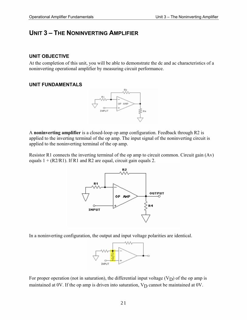
A noninverting amplifier is a closed-loop op amp configuration. Feedback through R2 is applied to the inverting terminal of the op amp. The input signal of the noninverting circuit is applied to the noninverting terminal of the op amp. Resistor R1 connects the inverting terminal of the op amp to circuit common. Circuit gain (Av) equals 1 + (R2/R1). If R1 and R2 are equal, circuit gain equals 2.
In a noninverting configuration, the output and input voltage polarities are identical.
For proper operation (not in saturation), the differential input voltage (VD) of the op amp is maintained at 0V. If the op amp is driven into saturation, VD cannot be maintained at 0V.

Operational Amplifier Fundamentals Unit 3 – The Noninverting Amplifier
22
Due to the very high input impedance of the op amp, a resistor (RIN) is usually connected between the positive terminal and circuit common. RIN prevents op amp saturation should the circuit input voltage (VI) be disconnected (referred to as a floating input). The input impedance of the circuit shown essentially equals the ohmic value of RIN. A noninverting op amp displays all the attributes of op amps in general: high input impedance, low output impedance, and high gain.
The circuit input voltage is applied to the positive op amp input. This means that the circuit summing junction is not at virtual ground but at a potential required to hold the differential input voltage (VD) at 0V.
To determine the circuit current distribution, apply Ohm's law. NOTE: VRIN is the same as VI, VR4 is the same as VO, and R1 and R2 form a voltage divider.

Operational Amplifier Fundamentals Unit 3 – The Noninverting Amplifier
23
NEW TERMS AND WORDS noninverting amplifier - a circuit using an active device to amplify but not invert an input signal.
EQUIPMENT REQUIRED F.A.C.E.T. base unit Multimeter Oscilloscope, dual trace Generator, sine wave OPERATIONAL AMPLIFIER FUNDAMENTALS circuit board
NOTES ______________________________________________________________________________ ______________________________________________________________________________ ______________________________________________________________________________ ______________________________________________________________________________ ______________________________________________________________________________ ______________________________________________________________________________ ______________________________________________________________________________ ______________________________________________________________________________ ______________________________________________________________________________ ______________________________________________________________________________

Operational Amplifier Fundamentals Unit 3 – The Noninverting Amplifier
24
Exercise 1 – Noninverting Amplifier DC Operation
EXERCISE OBJECTIVE When you have completed this exercise, you will be able to operate a noninverting operational amplifier using dc inputs. You will verify circuit operation with a multimeter.
EXERCISE DISCUSSION • The noninverting amplifier is a closed-loop op amp configuration. • Circuit gain (Av) is based on the ratio of R2 to R1: Av = 1 + (R2/R1). • Due to the noninverting operation, the output and input voltages have the same polarity. • R3 is adjusted to balance, or null, the circuit output (VO) to 0V. The circuit input must be
connected to circuit common. • A noninverting op amp amplifies an input voltage and does not invert the input voltage
polarity. • Since the circuit gain (Av) is 10, output voltage is +10 Vdc. • For nonsaturated operation, the differential input voltage (VD) must be 0V. • Since the op amp (+) input is at +1 Vdc, sufficient voltage is fed back (through R2) to
maintain VD at nearly 0V. • With respect to circuit common, both the (+) and (-) op amp inputs are at +1 Vdc. • To determine circuit current distribution, apply Ohm's law. • When the circuit input voltage (VI) is positive, electrons flow into the output terminal of the
op amp. • When VI is negative, electrons flow out of the output terminal of the op amp.

Operational Amplifier Fundamentals Unit 3 – The Noninverting Amplifier
25
NOTES ______________________________________________________________________________ ______________________________________________________________________________ ______________________________________________________________________________ ______________________________________________________________________________ ______________________________________________________________________________ ______________________________________________________________________________ ______________________________________________________________________________ ______________________________________________________________________________ ______________________________________________________________________________ ______________________________________________________________________________
Operational Amplifier Fundamentals Unit 3 – The Noninverting Amplifier
26
Exercise 2 – Noninverting Amplifier AC Operation
EXERCISE OBJECTIVE When you have completed this exercise, you will be able to operate a noninverting amplifier using ac inputs. You will verify circuit operation with an oscilloscope.
EXERCISE DISCUSSION • A noninverting amplifier amplifies an ac input signal. • Due to the noninverting configuration, output and input waveforms are not inverted or phase
shifted. • On the circuit board, the output voltage is defined by the equation
VO = VI x [1 + (R2/R1)] • If the input waveform amplitude is excessive, the op amp becomes saturated and distorts its
output waveform. • The active, undistorted peak-to-peak amplitude of an output waveform is limited by the
power supply voltage levels. • On the circuit board, the maximum output amplitude is 20 Vpk-pk.
NOTES ______________________________________________________________________________ ______________________________________________________________________________ ______________________________________________________________________________ ______________________________________________________________________________ ______________________________________________________________________________ ______________________________________________________________________________ ______________________________________________________________________________ ______________________________________________________________________________ ______________________________________________________________________________ ______________________________________________________________________________

Operational Amplifier Fundamentals Unit 3 – The Noninverting Amplifier
27
Exercise 3 – Noninverting Amplifier Response
EXERCISE OBJECTIVE When you have completed this exercise, you will be able to determine the gain/bandwidth characteristics of a noninverting operational amplifier. You will verify your results with an oscilloscope.
EXERCISE DISCUSSION • Gain-bandwidth (GBW) product and slew rate (SR) are two op amp specifications that affect
the operation of a noninverting amplifier. Slew rate will be examined in another unit. • For a noninverting amplifier, circuit gain multiplied by circuit band- width cannot exceed the
specified GBW product of the circuit op amp. • As the gain of the amplifier increases, circuit bandwidth decreases. • As the gain of the amplifier decreases, circuit bandwidth increases. • If the amplifier bandwidth is limited, its output voltage falls off (is reduced or attenuated),
and the waveform may be distorted. • The LF441 op amp has a specified GBW product of 1 MHz. • A capacitor placed across the circuit feedback resistor reduces the bandwidth ac gain of the
amplifier and ac gain becomes frequency dependent. • The breakpoint frequency of this circuit occurs at the frequency where XC (in ohms) equals
the value of R2. • The breakpoint is referred to as the -3 dB point of the circuit and defines the circuit
bandwidth frequency. • At the -3 dB point of a circuit, the output voltage is attenuated by the factor 0.707 (0.707 x
VO). • The formula dB = 20 log (VNEW/VINITIAL) expresses the change in output voltage. • VNEW is the final output voltage at the operating frequency, such as 100 kHz, where the
output voltage has decreased by 0.707. • VINITIAL is the starting output voltage at the reference frequency, such as 1 kHz.
Operational Amplifier Fundamentals Unit 3 – The Noninverting Amplifier
28
NOTES ______________________________________________________________________________ ______________________________________________________________________________ ______________________________________________________________________________ ______________________________________________________________________________ ______________________________________________________________________________ ______________________________________________________________________________ ______________________________________________________________________________ ______________________________________________________________________________ ______________________________________________________________________________ ______________________________________________________________________________
Operational Amplifier Fundamentals Unit 4 – The Voltage Follower
29
UNIT 4 – THE VOLTAGE FOLLOWER
UNIT OBJECTIVE At the completion of this unit, you will be able to operate an operational amplifier circuit configured as a voltage follower or a gain-of-one inverting amplifier.
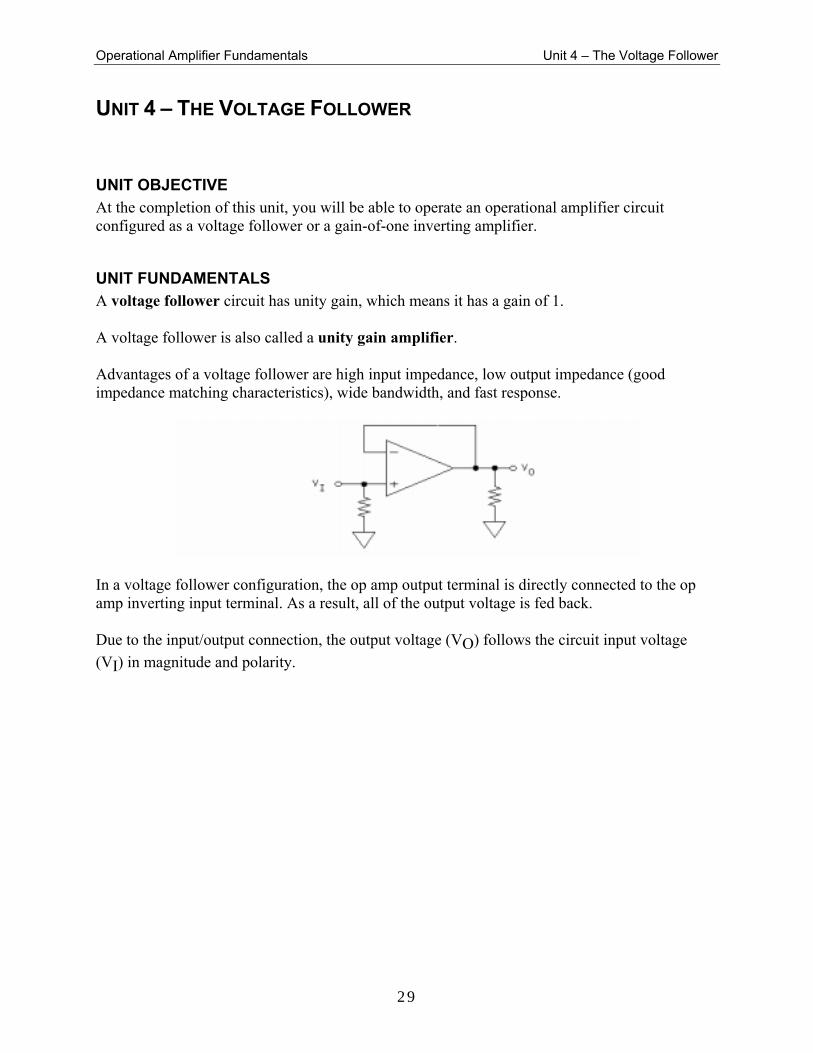
UNIT FUNDAMENTALS A voltage follower circuit has unity gain, which means it has a gain of 1. A voltage follower is also called a unity gain amplifier. Advantages of a voltage follower are high input impedance, low output impedance (good impedance matching characteristics), wide bandwidth, and fast response.
In a voltage follower configuration, the op amp output terminal is directly connected to the op amp inverting input terminal. As a result, all of the output voltage is fed back. Due to the input/output connection, the output voltage (VO) follows the circuit input voltage (VI) in magnitude and polarity.

Operational Amplifier Fundamentals Unit 4 – The Voltage Follower
30
The voltage at the op amp inverting terminal equals the output voltage (VO). VO follows the circuit input voltage (VI). VD, the op amp differential input voltage, is 0V. The GBW product of an op amp is specified at unity gain. A voltage follower circuit operates with unity gain. Therefore, the circuit bandwidth essentially equals the specified op amp GBW product (1 MHz for the LF441 op amp). The ability of an op amp voltage follower to accurately duplicate an input voltage is related to levels of operation called small-signaland large-signal. Typically, small-signal refers to voltages with amplitudes equal to or less than 1 Vpk-pk. Typically, large-signal refers to voltages with amplitudes between 10 Vpk-pk and 20 Vpk-pk. Small-signal operation is primarily related to the GBW product of an op amp. Large-signal operation is primarily related to op amp slew rate and full-power bandwidth.

Operational Amplifier Fundamentals Unit 4 – The Voltage Follower
31
This voltage follower configuration is used to measure the effects of op amp slew rate and full-power bandwidth on an input signal. A voltage follower configuration generates an output signal (VO) equal to and in phase with the circuit input signal (VI).
However, some applications require unity gain with phase inversion. An op amp configured as a unity gain inverting amplifier meets this requirement.
On your circuit board, the VOLTAGE FOLLOWER circuit block can be configured for either noninverting or inverting operation. Due to the low output offset voltage values of the LF441 op amp, the VOLTAGE FOLLOWER circuit block does not require a nulling circuit.

Operational Amplifier Fundamentals Unit 4 – The Voltage Follower
32
NEW TERMS AND WORDS voltage follower - a circuit in which the output voltage is equal to and in phase with the circuit input voltage. unity gain amplifier - an amplifier configured with a gain of 1. small-signal - output voltages typically less than 1 Vpk-pk. large-signal - typical output voltages between 10 Vpk-pk and 20 Vpk-pk. full-power bandwidth - the highest large-signal frequency at which the amplifier delivers rated output without distortion. Fractional gain - a gain that is less than unity. slope - change in voltage divided by change in time. rated output - the maximum output voltages at which an op amp is designed to operate.
EQUIPMENT REQUIRED F.A.C.E.T. base unit Multimeter Oscilloscope, dual trace Generator sine/square wave OPERATIONAL AMPLIFIER FUNDAMENTALS circuit board
NOTES ______________________________________________________________________________ ______________________________________________________________________________ ______________________________________________________________________________ ______________________________________________________________________________ ______________________________________________________________________________ ______________________________________________________________________________ ______________________________________________________________________________ ______________________________________________________________________________ ______________________________________________________________________________ ______________________________________________________________________________

Operational Amplifier Fundamentals Unit 4 – The Voltage Follower
33
Exercise 1 – Voltage Follower DC Operation
EXERCISE OBJECTIVE When you have completed this exercise, you will be able to operate a voltage follower using dc voltages. You will verify your results with a multimeter.
EXERCISE DISCUSSION • Voltage follower output voltage (VO) equals the input voltage (VI). Output voltage (VO) is
identical to the polarity of VI. • High input impedance reduces loading. • Noise and stray pickup, which might develop across the high-impedance op-amp input are
reduced when input, impedance is lowered by an input resistor. • When output voltage (VO) is stable and the op amp is not saturated, differential input voltage
(VD) is intrinsically 0. • If VD is greater than 0V, the op amp saturates and cannot duplicate the input (VI). • A change of input voltage (VI) causes a voltage to develop across the differential input of the
op amp. It responds by changing the output voltage (VO). Since VO is fed back to the input, VO continues to affect VI until VD is restored to 0V; additional voltage change is then no longer required, and the output voltage is stabilized at a new level.
NOTES ______________________________________________________________________________ ______________________________________________________________________________ ______________________________________________________________________________ ______________________________________________________________________________ ______________________________________________________________________________ ______________________________________________________________________________ ______________________________________________________________________________ ______________________________________________________________________________ ______________________________________________________________________________ ______________________________________________________________________________
Operational Amplifier Fundamentals Unit 4 – The Voltage Follower
34
Exercise 2 – Inverting Gain-of-One Amplifier
EXERCISE OBJECTIVE When you have completed this exercise, you will be able to operate an inverting gain-of-one amplifier using dc voltages. You will verify circuit operation with a voltmeter.
EXERCISE DISCUSSION • An inverting amplifier can be configured to provide unity gain. • Circuit gain equals R3/R1. If R3 and R1 are equal in value, the circuit gain equals one. • Resistor R2 is added to the circuit to reduce the input bias current effect. The value of R2
equals the parallel combination of R3 and R1: R2 = (R3 x R1)/(R3 + R1). NOTE: Input bias current flowing through R1 generates a voltage (VR1) that appears at the output. • Fractional gain, a gain of less than one, results if the value of R3 is less than the value of R1. • Since the circuit output voltage is less than the circuit input voltage, the configuration acts as
an attenuator. • To determine the current distribution of the gain-of-one inverting amplifier, apply Ohm's law
(I = V/R) to the circuit. • A positive input voltage to an inverting gain-of-one amplifier generates a negative output
voltage. Electrons flow out of the op amp output terminal. • When U1 is not saturated, VO tracks VI, and VD is at 0V. • U1 is zero-based (R2 connected to common); therefore, the inverting terminal of U1 is at
virtual ground and serves as the circuit summing junction. • If U1 is saturated (VO greater than 10 Vdc), VO cannot track VI, and VD is greater than 0V.

Operational Amplifier Fundamentals Unit 4 – The Voltage Follower
35
NOTES ______________________________________________________________________________ ______________________________________________________________________________ ______________________________________________________________________________ ______________________________________________________________________________ ______________________________________________________________________________ ______________________________________________________________________________ ______________________________________________________________________________ ______________________________________________________________________________ ______________________________________________________________________________ ______________________________________________________________________________

Operational Amplifier Fundamentals Unit 4 – The Voltage Follower
36
Exercise 3 – Voltage Follower AC Characteristics
EXERCISE OBJECTIVE When you have completed this exercise, you will be able to determine the effects of slew rate and full-power bandwidth on a voltage follower. You will observe the effects on an oscilloscope.
EXERCISE DISCUSSION • Slew rate (SR) specifies maximum rate-of-change in output voltage over a period of time.
Mathematically, SR is equivalent to the slope of a waveform. • Slew rate (SR) is defined as a change in output voltage divided by the time interval during
which the voltage change occurs. For this pair of parameters, SR is given in units of volts/time.
• The graph illustrates how slew is measured. The calculation determines the slope of the line. SR is given in volts/microsecond (V/µs).
• If, for example, output voltage changes by 10V in 10 µs, the slew rate of the circuit is 1 V/µs • Ideal op amps have an infinite slew rate: the output would instantaneously follow any change
at the input. • An ideal square wave has instantaneous rise and fall times. • The LF441 op amp used on the circuit board has a specified slew rate of 1 V/µs. Generally,
this means that the op amp output voltage cannot change faster than 1V in less than 1 µs. • Slew rate decreases rise and fall times of a square wave. For a slew rate of 1 V/µs, it would
take 10 µs for a 10V swing to occur. • If an op amp circuit has an SR of 5 V/µs and its square wave input has rise and fall times of 1
V/µs, the circuit can duplicate the input waveform. • When the circuit SR is equal to or greater than the rate of change in the input waveform, the
circuit output waveform tracks (reproduces) the input waveform. • When circuit SR is less than the rate of change of an input waveform, the output waveform
does not fully track (reproduce) the input waveform. The "squareness" of the waveform is reduced.
• For a given slew-rate-limited circuit, an output waveform becomes triangular and decreases in amplitude as input frequency increases.
• Slew rate limitations also affect sinusoidal waveforms. On a sinusoidal waveform, the slope is maximum at the zero crossing points and zero at the peak points of the waveform.
• The slope of a sinusoidal waveform always changes. • Slope defines a rate of change (volts per unit of time). Therefore, slope is also frequency
dependent. If the frequency of a constant amplitude sinusoidal waveform increases (period decreases), the slope of the waveform increases.

Operational Amplifier Fundamentals Unit 4 – The Voltage Follower
37
• The rated output of an op amp is affected by a parameter called full-power bandwidth: the maximum frequency at which an op amp can produce a large-signal (10 Vpk) output without significant distortion.
• An increase in the amplitude of a sinusoidal waveform increases the rate of change of the waveform. This increase can cause the amplifier to distort the waveform because of slew rate limitations.
• At the full-power bandwidth frequency, the output waveform of the op amp goes out of phase with the input waveform. However, there is little effect on output amplitude.
• If the op amp operates below the full-power bandwidth, Vo is in phase with Vi but not distorted.
• When input frequency is greater than the full-power bandwidth, the output waveform becomes slew-rate limited (and appears triangular) and its amplitude decreases.
NOTES ______________________________________________________________________________ ______________________________________________________________________________ ______________________________________________________________________________ ______________________________________________________________________________ ______________________________________________________________________________ ______________________________________________________________________________ ______________________________________________________________________________ ______________________________________________________________________________ ______________________________________________________________________________ ______________________________________________________________________________
Operational Amplifier Fundamentals Unit 4 – The Voltage Follower
38

Operational Amplifier Fundamentals Unit 5 – The Inverting Summer
39
UNIT 5 – THE INVERTING SUMMER
UNIT OBJECTIVE At the completion of this unit, you will be able to describe the operation of an inverting summing amplifier using a three-input op amp summing configuration.
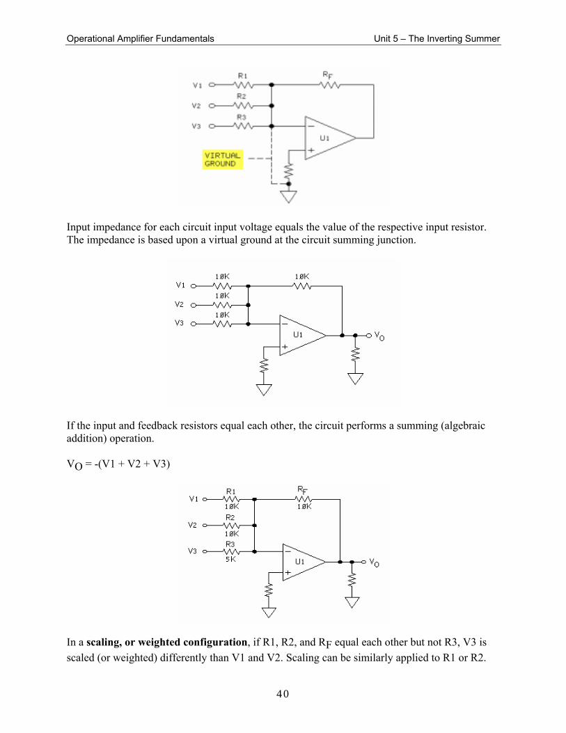
UNIT FUNDAMENTALS An inverting summing amplifier is a multiple input inverting op amp circuit. The circuit output voltage is proportional to the algebraic sum of the input voltages. The polarity of the circuit output voltage is opposite that of the summed input voltages.
The junction formed by the input resistors, feedback resistor, and the op amp inverting terminal is the circuit summing point. Direct summation of the input voltages and feed-back voltage occurs at the circuit summing junction. The circuit summing junction is at virtual ground (the op amp is zero based) because the noninverting terminal is referenced to circuit common.
Circuit output voltage is proportional to the sum of each input voltage multiplied by the ratio of RF to the respective input resistor (Rx). VO = -[(RF/R1) x V1] + [(RF/R2) x V2] + [(RF/R3) x V3]
Operational Amplifier Fundamentals Unit 5 – The Inverting Summer
40
Input impedance for each circuit input voltage equals the value of the respective input resistor. The impedance is based upon a virtual ground at the circuit summing junction.
If the input and feedback resistors equal each other, the circuit performs a summing (algebraic addition) operation. VO = -(V1 + V2 + V3)
In a scaling, or weighted configuration, if R1, R2, and RF equal each other but not R3, V3 is scaled (or weighted) differently than V1 and V2. Scaling can be similarly applied to R1 or R2.

Operational Amplifier Fundamentals Unit 5 – The Inverting Summer
41
If R3, R2, and R1 equal each other but RF equals the average value of the input resistors, VO equals the average value of the input voltages. VO = -[(V1 + V2 + V3)/3] Op amp saturation levels limit the maximum circuit output voltage. If the product of any one input voltage and its respective circuit gain factor is excessive, the op amp saturates.
NEW TERMS AND WORDS inverting summing amplifier - an inverting op amp configuration that algebraically combines two or more input voltages. scaling, or weighted configuration - a summing amplifier configuration that allows a certain input voltage to have more influence on the output voltage than another input voltage. summing configuration - a summing amplifier configuration that generates an output voltage equal to the algebraic sum of the input voltages. averaging configuration - a summing amplifier configuration that generates an output voltage equal to the average value of the circuit input voltages.
EQUIPMENT REQUIRED F.A.C.E.T. base unit Multimeter OPERATIONAL AMPLIFIER FUNDAMENTALS circuit board

Operational Amplifier Fundamentals Unit 5 – The Inverting Summer
42
NOTES ______________________________________________________________________________ ______________________________________________________________________________ ______________________________________________________________________________ ______________________________________________________________________________ ______________________________________________________________________________ ______________________________________________________________________________ ______________________________________________________________________________ ______________________________________________________________________________ ______________________________________________________________________________ ______________________________________________________________________________

Operational Amplifier Fundamentals Unit 5 – The Inverting Summer
43
Exercise 1 – Amplifier Operation
EXERCISE OBJECTIVE When you have completed this exercise, you will be able to operate an inverting summing amplifier. You will verify circuit operation with a multimeter.
EXERCISE DISCUSSION • A summing amplifier combines multiple input voltages and applies individual gain factors to
each input. • To minimize summing errors, R4 is added to the circuit. R4 equals the parallel combination
of R1, R2, R3, and R5. • The summing configuration generates an output voltage equal to the algebraic sum of each
circuit input voltage multiplied by its respective circuit gain factor. • Due to the inverting configuration, the polarity of the summed input voltages is inverted at
the circuit output. • U1, working through the feedback path, keeps the differential input voltage (VD) at 0V. • If VD is greater than 0V (positive or negative), U1 is driven into saturation. • One of the circuit inputs can be used to null, or trim, the circuit offset voltage to 0V. • Circuit input, feedback, and load current distribution depend on the magnitude and polarity
of the input and output voltages. • Apply Ohm's law to determine the magnitude of each current. • For positive input voltages, the summed voltage polarity is positive, and electrons flow out of
the op amp output terminal. • For negative input voltages, the summed voltage polarity is negative, and electrons flow into
the op amp output terminal. • If the circuit input voltages are positive and negative, electrons flow in either direction. • The direction of the op amp output terminal current is based on the resultant polarity of the
summed input voltages.

Operational Amplifier Fundamentals Unit 5 – The Inverting Summer
44
NOTES ______________________________________________________________________________ ______________________________________________________________________________ ______________________________________________________________________________ ______________________________________________________________________________ ______________________________________________________________________________ ______________________________________________________________________________ ______________________________________________________________________________ ______________________________________________________________________________ ______________________________________________________________________________ ______________________________________________________________________________

Operational Amplifier Fundamentals Unit 5 – The Inverting Summer
45
Exercise 2 – Averaging
EXERCISE OBJECTIVE When you have completed this exercise, you will be able to operate an inverting summing amplifier configured for weighting or averaging application. You will verify your results with a multimeter.
EXERCISE DISCUSSION • A fundamental inverting summing op amp can be configured for summing, scaling
(weighting), or averaging operations. • The circuit is configured as a unity gain inverting summing amplifier. • In a unity gain inverting summing amplifier where R2, R1, and RF are equal in value, the
circuit output voltage equals the sum of the input voltages [VO = - (V1 + V2)]. • If the inputs have different gains, the input with the greater gain has more weight. • If the input resistors are equal and the feedback resistor equals the parallel value of the input
resistors, VO equals the average of the circuit input voltages. • Any number of input voltages can be averaged if the circuit resistor ratios are maintained.
NOTES ______________________________________________________________________________ ______________________________________________________________________________ ______________________________________________________________________________ ______________________________________________________________________________ ______________________________________________________________________________ ______________________________________________________________________________ ______________________________________________________________________________ ______________________________________________________________________________ ______________________________________________________________________________ ______________________________________________________________________________

Operational Amplifier Fundamentals Unit 5 – The Inverting Summer
46

Operational Amplifier Fundamentals Unit 6 – The Noninverting Summing Amplifier
47
UNIT 6 – THE NONINVERTING SUMMING AMPLIFIER
UNIT OBJECTIVE At the completion of this unit, you will be able to describe the operation of a noninverting summing amplifier.
UNIT FUNDAMENTALS
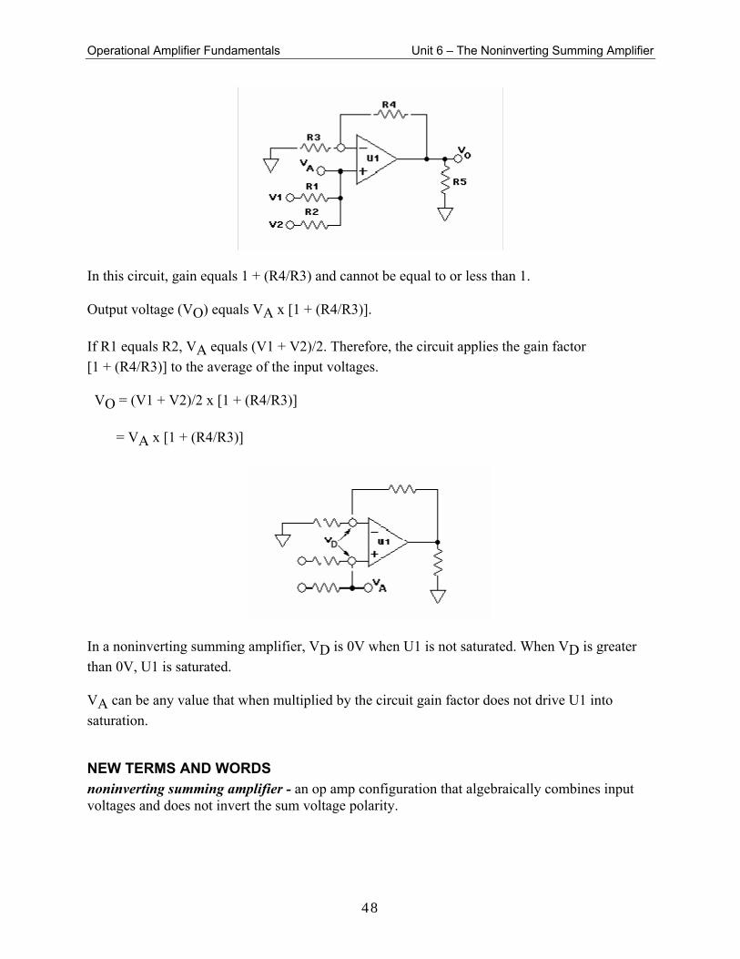
In a noninverting summing amplifier, the (-) terminal acts as the op amp summing junction. The (+) terminal acts as the summing point (VA) of the individual circuit input voltages. VA is multiplied by the circuit gain factor [1 + (RF/R1)] to generate the output voltage (VO).
Due to the high impedance of U1, VA is determined by the superposition theorem. However, if R1 and R2 are equal in value, VA = (V1 + V2)/2. NOTE: V1, V2, and VA are measured with respect to circuit common. U1 is not zero based because the (+) input terminal is not returned to circuit common. VA can be greater than 0V (positive) or less than 0V (negative).
Operational Amplifier Fundamentals Unit 6 – The Noninverting Summing Amplifier
48
In this circuit, gain equals 1 + (R4/R3) and cannot be equal to or less than 1. Output voltage (VO) equals VA x [1 + (R4/R3)]. If R1 equals R2, VA equals (V1 + V2)/2. Therefore, the circuit applies the gain factor [1 + (R4/R3)] to the average of the input voltages. VO = (V1 + V2)/2 x [1 + (R4/R3)] = VA x [1 + (R4/R3)]
In a noninverting summing amplifier, VD is 0V when U1 is not saturated. When VD is greater than 0V, U1 is saturated. VA can be any value that when multiplied by the circuit gain factor does not drive U1 into saturation.
NEW TERMS AND WORDS noninverting summing amplifier - an op amp configuration that algebraically combines input voltages and does not invert the sum voltage polarity.
Operational Amplifier Fundamentals Unit 6 – The Noninverting Summing Amplifier
49
EQUIPMENT REQUIRED F.A.C.E.T. base unit Multimeter OPERATIONAL AMPLIFIER FUNDAMENTALS circuit board
NOTES ______________________________________________________________________________ ______________________________________________________________________________ ______________________________________________________________________________ ______________________________________________________________________________ ______________________________________________________________________________ ______________________________________________________________________________ ______________________________________________________________________________ ______________________________________________________________________________ ______________________________________________________________________________ ______________________________________________________________________________

Operational Amplifier Fundamentals Unit 6 – The Noninverting Summing Amplifier
50
Exercise 1 – Noninverting Summing Amplifier Operation
EXERCISE OBJECTIVE When you have completed this exercise, you will be able to operate a noninverting summing amplifier. You will verify your results with a multimeter.
EXERCISE DISCUSSION • The output equation for the two-input noninverting summing amplifier used in this exercise
is: VO = [(V1 + V2)/2] x [1 + (R4/R3)] • The output voltage polarity equals the polarity of the average input voltage
[VA = (V1 + V2)/2]. • Due to feedback, the voltage at the summing point equals VA. Therefore, the differential
input voltage (VD) equals 0V. • Ohm's law can be applied to determine the current distribution of a noninverting summing
amplifier circuit.
NOTES ______________________________________________________________________________ ______________________________________________________________________________ ______________________________________________________________________________ ______________________________________________________________________________ ______________________________________________________________________________ ______________________________________________________________________________ ______________________________________________________________________________ ______________________________________________________________________________ ______________________________________________________________________________ ______________________________________________________________________________

Operational Amplifier Fundamentals Unit 6 – The Noninverting Summing Amplifier
51
Exercise 2 – Summing and Averaging Operation
EXERCISE OBJECTIVE When you have completed this exercise, you will be able to configure a noninverting amplifier as a voltage averaging or summing circuit. You will verify your results with a multimeter.
EXERCISE DISCUSSION • In a two-input noninverting summing amplifier, V1 and V2 are combined at VA because of
the high input impedance of the op amp. • If the circuit is in the voltage follower configuration, the gain is 1. • If R1 equals R2, then VA equals (V1 + V2)/2. • If R1 and R2 are not equal, then VA is determined by measurement or by application of the
superposition theorem. • If the input resistors are equal in value, any number of circuit input voltages can be averaged. • VO equals the algebraic sum of the input voltages divided by the number of input voltages.
NOTES ______________________________________________________________________________ ______________________________________________________________________________ ______________________________________________________________________________ ______________________________________________________________________________ ______________________________________________________________________________ ______________________________________________________________________________ ______________________________________________________________________________ ______________________________________________________________________________ ______________________________________________________________________________ ______________________________________________________________________________

Operational Amplifier Fundamentals Unit 6 – The Noninverting Summing Amplifier
52

Operational Amplifier Fundamentals Unit 7 – The Difference Amplifier
53
UNIT 7 – THE DIFFERENCE AMPLIFIER
UNIT OBJECTIVE At the completion of this unit, you will be able to describe the operation of a difference amplifier by using a typical operational amplifier circuit.
UNIT FUNDAMENTALS
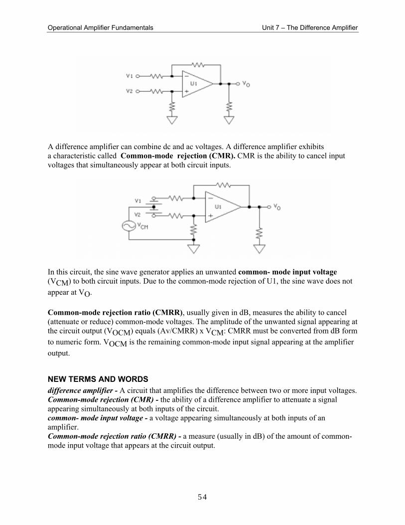
The difference amplifier shown is a two-input circuit that amplifies the difference between V1 and V2. V1 is connected to the inverting side of U1, and V2 is connected to the noninverting side of U1.
When R1, R2, R4, and R5 are equal in value, the difference amplifier subtracts V1 and V2.
VO = V2 - V1 In practice, the input impedance for V1 equals the ohmic value of R1. The input impedance for V2 equals the ohmic value of R2 + R4. A difference amplifier circuit combines the gain effect from the inverting and noninverting resistor ratios. For V1, VO equals -[V1 x (R5/R1)]. For V2, VO equals V2 x [R4/(R2 + R4)] x [1 + (R5/R1)].
Operational Amplifier Fundamentals Unit 7 – The Difference Amplifier
54
A difference amplifier can combine dc and ac voltages. A difference amplifier exhibits a characteristic called Common-mode rejection (CMR). CMR is the ability to cancel input voltages that simultaneously appear at both circuit inputs.
In this circuit, the sine wave generator applies an unwanted common- mode input voltage (VCM) to both circuit inputs. Due to the common-mode rejection of U1, the sine wave does not appear at VO. Common-mode rejection ratio (CMRR), usually given in dB, measures the ability to cancel (attenuate or reduce) common-mode voltages. The amplitude of the unwanted signal appearing at the circuit output (VOCM) equals (Av/CMRR) x VCM: CMRR must be converted from dB form to numeric form. VOCM is the remaining common-mode input signal appearing at the amplifier output.
NEW TERMS AND WORDS difference amplifier - A circuit that amplifies the difference between two or more input voltages. Common-mode rejection (CMR) - the ability of a difference amplifier to attenuate a signal appearing simultaneously at both inputs of the circuit. common- mode input voltage - a voltage appearing simultaneously at both inputs of an amplifier. Common-mode rejection ratio (CMRR) - a measure (usually in dB) of the amount of common-mode input voltage that appears at the circuit output.

Operational Amplifier Fundamentals Unit 7 – The Difference Amplifier
55
EQUIPMENT REQUIRED F.A.C.E.T. base unit Multimeter Oscilloscope, dual trace Generator, sine wave OPERATIONAL AMPLIFIER FUNDAMENTALS circuit board
NOTES ______________________________________________________________________________ ______________________________________________________________________________ ______________________________________________________________________________ ______________________________________________________________________________ ______________________________________________________________________________ ______________________________________________________________________________ ______________________________________________________________________________ ______________________________________________________________________________ ______________________________________________________________________________ ______________________________________________________________________________
Operational Amplifier Fundamentals Unit 7 – The Difference Amplifier
56
Exercise 1 – Difference Amplifier DC Operation
EXERCISE OBJECTIVE When you have completed this exercise, you will be able to operate a difference amplifier using dc voltages. You will verify your results with a multimeter.
EXERCISE DISCUSSION • The difference amplifier circuit on the circuit board has resistors R1, R2, R4, and R5 equal to
each other. • Due to the resistor values, VO equals V2 - V1, or the difference between the input voltages. • The output voltage polarity is determine by the relationship between the noninverting input
voltage (V2) to the inverting input voltage (V1). • The V2 polarity dominates the V1 polarity and determines the output voltage polarity. • The following relationships apply (U1 is not saturated) to the difference amplifier circuit.
VO = VA - V1 VA = (V2 x R4)/(R2 + R4) VD = 0V VA = VR4
NOTES ______________________________________________________________________________ ______________________________________________________________________________ ______________________________________________________________________________ ______________________________________________________________________________ ______________________________________________________________________________ ______________________________________________________________________________ ______________________________________________________________________________ ______________________________________________________________________________ ______________________________________________________________________________ ______________________________________________________________________________

Operational Amplifier Fundamentals Unit 7 – The Difference Amplifier
57
Exercise 2 – Difference Amplifier AC Operation
EXERCISE OBJECTIVE When you have completed this exercise, you will be able to operate a difference amplifier using ac voltages. You will verify your results with an oscilloscope.
EXERCISE DISCUSSION • The difference amplifier combines input waveforms and accounts for amplitude and phase. • If R1, R2, R4, and R5 are equal in value, Vo equals V2 - V1. • If V2 and V1 are identical (in amplitude and phase) ac waveforms, Vo is essentially 0V. • Vo is 0V because of the common-mode rejection capability of U1. • The common-mode rejection capability of an op amp is an advantage because a common-
mode input voltage has a small effect on circuit output voltage. • If V2 has greater amplitude than V1, Vo is in phase with V2 and lower in amplitude then
either V2 or V1. • If V2 has less amplitude than V1, Vo is in phase with V1 and lower in amplitude than either
V2 or V1. • If V2 and V1 have equal amplitudes and are 180° out of phase, then Vo is in phase with V2.
In addition, Vo equals 2 x V1 or 2 x V2. • When V2 and V1 are out of phase, V1 (the inverting input) adds to the magnitude of V2 (the
noninverting input). V2 dominates V1, and Vo is in phase with V2. • Based on the V2 - V1 relationship of a difference amplifier, out-of-phase inputs (not
common-mode) are added.

Operational Amplifier Fundamentals Unit 7 – The Difference Amplifier
58
NOTES ______________________________________________________________________________ ______________________________________________________________________________ ______________________________________________________________________________ ______________________________________________________________________________ ______________________________________________________________________________ ______________________________________________________________________________ ______________________________________________________________________________ ______________________________________________________________________________ ______________________________________________________________________________ ______________________________________________________________________________

Operational Amplifier Fundamentals Unit 8 – Voltage Comparators
59
UNIT 8 – VOLTAGE COMPARATORS
UNIT OBJECTIVE At the completion of this unit, you will be able to describe the operation of an operational amplifier comparator circuit.
UNIT FUNDAMENTALS A voltage comparator circuit compares an input voltage to a reference voltage and indicates whether the input is greater than, equal to, or less than the reference voltage. Voltage comparators are typically used as level detectors or squaring circuits. Level detectors indicate when a voltage crosses a specific set point. Squaring circuits convert slow rise or fall time wave-forms into high slewing waveforms.
On this open-loop comparator, VI is compared to the reference voltage (VREF). VREF is connected to the non- inverting terminal of U1. Therefore, U1 is not zero based, but has a trigger point equal to VREF. In this circuit, U1 tends to saturate due to the very high open-loop gain. VD is not 0V if U1 is saturated. When VI is more positive than VREF, VD is greater than 0V, and VO switches to -VSAT. When VI is more negative than VREF, VD is greater than 0V, and VO switches to +VSAT.
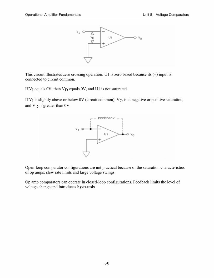
Operational Amplifier Fundamentals Unit 8 – Voltage Comparators
60
This circuit illustrates zero crossing operation: U1 is zero based because its (+) input is connected to circuit common. If VI equals 0V, then VD equals 0V, and U1 is not saturated. If VI is slightly above or below 0V (circuit common), VO is at negative or positive saturation, and VD is greater than 0V.
Open-loop comparator configurations are not practical because of the saturation characteristics of op amps: slew rate limits and large voltage swings. Op amp comparators can operate in closed-loop configurations. Feedback limits the level of voltage change and introduces hysteresis.
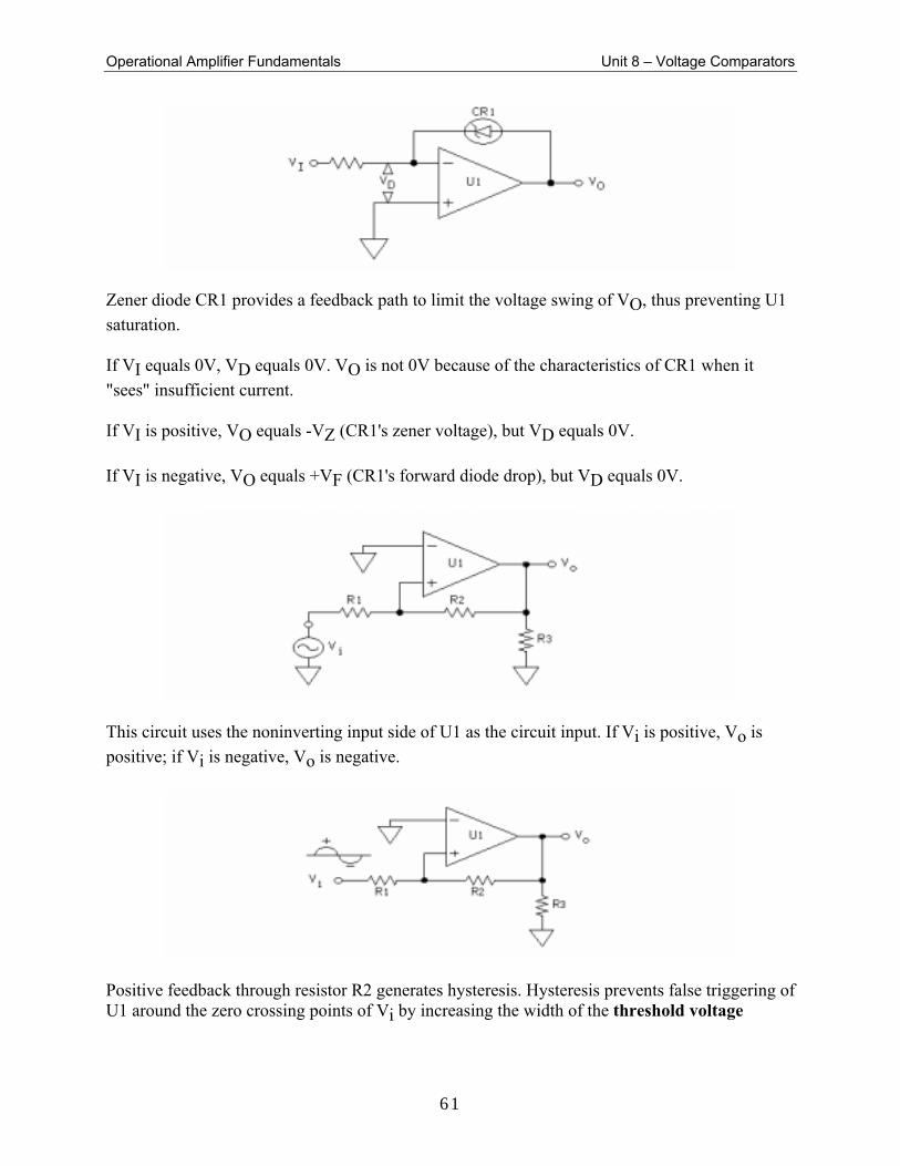
Operational Amplifier Fundamentals Unit 8 – Voltage Comparators
61
Zener diode CR1 provides a feedback path to limit the voltage swing of VO, thus preventing U1 saturation. If VI equals 0V, VD equals 0V. VO is not 0V because of the characteristics of CR1 when it "sees" insufficient current. If VI is positive, VO equals -VZ (CR1's zener voltage), but VD equals 0V. If VI is negative, VO equals +VF (CR1's forward diode drop), but VD equals 0V.
This circuit uses the noninverting input side of U1 as the circuit input. If Vi is positive, Vo is positive; if Vi is negative, Vo is negative.
Positive feedback through resistor R2 generates hysteresis. Hysteresis prevents false triggering of U1 around the zero crossing points of Vi by increasing the width of the threshold voltage
Operational Amplifier Fundamentals Unit 8 – Voltage Comparators
62
NEW TERMS AND WORDS voltage comparator - A circuit that compares an input voltage to a reference voltage. level detectors - circuits that compare the level of a signal to a reference level. hysteresis - a small amount of feedback that provides stability. threshold voltage - a narrow voltage band centered between the positive and negative switching levels of a comparator. trip point - the point within the threshold band where the output of a comparator switches from one level to the other. Schmitt trigger - comparator type that uses hysteresis to provide stability around a circuit trigger point.
EQUIPMENT REQUIRED F.A.C.E.T. base unit Multimeter Oscilloscope, dual trace OPERATIONAL AMPLIFIER FUNDAMENTALS circuit board Generator, sine/square wave
NOTES ______________________________________________________________________________ ______________________________________________________________________________ ______________________________________________________________________________ ______________________________________________________________________________ ______________________________________________________________________________ ______________________________________________________________________________ ______________________________________________________________________________ ______________________________________________________________________________ ______________________________________________________________________________ ______________________________________________________________________________
Operational Amplifier Fundamentals Unit 8 – Voltage Comparators
63
Exercise 1 – Open-Loop Operation
EXERCISE OBJECTIVE When you have completed this exercise, you will be able to operate an open-loop comparator. You will verify your results with a multimeter and an oscilloscope.
EXERCISE DISCUSSION • U1 has very high gain: 50,000 or more. • When configured for open-loop operation, U1 tends to saturate. • When input voltage equals reference voltage the output voltage is at positive saturation. • When input voltage is negative with respect to reference voltage the output voltage is at
positive saturation. • When input voltage is positive with respect to reference voltage the output voltage is at
negative saturation. • U1 switches between +VSAT and -VSAT as VI is adjusted slightly below or above VREF. This
point of operation is called the circuit trip point. • Since the range around the circuit trip point is small, the circuit threshold voltage is narrow.
NOTES ______________________________________________________________________________ ______________________________________________________________________________ ______________________________________________________________________________ ______________________________________________________________________________ ______________________________________________________________________________ ______________________________________________________________________________ ______________________________________________________________________________ ______________________________________________________________________________ ______________________________________________________________________________ ______________________________________________________________________________

Operational Amplifier Fundamentals Unit 8 – Voltage Comparators
64
Exercise 2 – Zener-Clamped Operation
EXERCISE OBJECTIVE When you have completed this exercise, you will be able to operate a zener-clamped op amp comparator circuit using dc and ac voltages. You will verify your results with an oscilloscope.
EXERCISE DISCUSSION • In the circuit for this exercise, a zener diode (CR1) completes the feedback path for U1. • U1 is zero based because its noninverting terminal is connected to circuit common.
Therefore, the circuit reference voltage is 0V. • If VI is positive (greater than 0V), VO swings in a negative direction toward -VSAT. • When VO approximately equals the zener breakdown voltage (VZ), CR1 conducts and
provides negative feedback. The feedback clamps VO to the value of VZ and prevents negative saturation.
• Based on the placement of CR1 (anode lead to U1 output terminal) in the circuit, VO switches between -VZ and +VF.
• A zener-diode-clamped circuit controls the levels of a sine wave or square wave input signal.
NOTES ______________________________________________________________________________ ______________________________________________________________________________ ______________________________________________________________________________ ______________________________________________________________________________ ______________________________________________________________________________ ______________________________________________________________________________ ______________________________________________________________________________ ______________________________________________________________________________ ______________________________________________________________________________ ______________________________________________________________________________
Operational Amplifier Fundamentals Unit 8 – Voltage Comparators
65
Exercise 3 – Square Wave Converter
EXERCISE OBJECTIVE When you have completed this exercise, you will be able to operate a sine wave to square wave converter. You will verify your results with an oscilloscope.
EXERCISE DISCUSSION • U1 is configured as an open-loop comparator that uses positive feedback and is referred to as
a Schmitt trigger. • Vi is converted from a sine wave into a square wave. Vo switches between +VSAT and -VSAT
and is in phase with Vi. • Positive feedback voltage (VTH) is provided by hysteresis resistor RH. Two trigger points are
established by the positive feedback. • VTH provides a voltage at the noninverting input of U1. Therefore, the circuit is not zero
based. • Hysteresis, or positive feedback, creates a window, or band, through which Vi must cross
before the comparator switches Vo. • Based on a specific hysteresis level, a switch in Vo occurs at trigger points A and B. • Vo cannot switch back until Vi crosses a trigger point. Within the window, variations of Vi
do not cause U1 to switch. • The voltage difference between points A and B, labeled +VTT and -VTT, equals the circuit
hysteresis voltage. • An increase of positive feedback increases the width of the hysteresis window. • A decrease of positive feedback decreases the width of the hysteresis window. • Hysteresis reduces the sensitivity of a comparator, increasing the noise immunity of the
circuit. • Based on Vi, a zero based comparator (no hysteresis) generates many changes in Vo. The
number of transitions in Vo decreases as hysteresis increases. • Two equations, based on the saturation level of U1, define the circuit trigger voltages • (+VT and -VT). +VT = +VSAT/(R2/R1) -VT = -VSAT/(R2/R1) • The trigger voltages are based on the saturation voltage of U1. Therefore, the trigger points
are not symmetrical and vary from op amp to op amp.

Operational Amplifier Fundamentals Unit 8 – Voltage Comparators
66
NOTES ______________________________________________________________________________ ______________________________________________________________________________ ______________________________________________________________________________ ______________________________________________________________________________ ______________________________________________________________________________ ______________________________________________________________________________ ______________________________________________________________________________ ______________________________________________________________________________ ______________________________________________________________________________ ______________________________________________________________________________

APPENDIX A – SAFETY
Safety is everyone’s responsibility. All must cooperate to create the safest possible working environment. Students must be reminded of the potential for harm, given common sense safety rules, and instructed to follow the electrical safety rules. Any environment can be hazardous when it is unfamiliar. The F.A.C.E.T. computer-based laboratory may be a new environment to some students. Instruct students in the proper use of the F.A.C.E.T. equipment and explain what behavior is expected of them in this laboratory. It is up to the instructor to provide the necessary introduction to the learning environment and the equipment. This task will prevent injury to both student and equipment. The voltage and current used in the F.A.C.E.T. Computer-Based Laboratory are, in themselves, harmless to the normal, healthy person. However, an electrical shock coming as a surprise will be uncomfortable and may cause a reaction that could create injury. The students should be made aware of the following electrical safety rules. 1. Turn off the power before working on a circuit. 2. Always confirm that the circuit is wired correctly before turning on the power. If required,
have your instructor check your circuit wiring. 3. Perform the experiments as you are instructed: do not deviate from the documentation. 4. Never touch “live” wires with your bare hands or with tools. 5. Always hold test leads by their insulated areas. 6. Be aware that some components can become very hot during operation. (However, this is not
a normal condition for your F.A.C.E.T. course equipment.) Always allow time for the components to cool before proceeding to touch or remove them from the circuit.
7. Do not work without supervision. Be sure someone is nearby to shut off the power and provide first aid in case of an accident.
8. Remove power cords by the plug, not by pulling on the cord. Check for cracked or broken insulation on the cord.

THIS THIS