operation and control of cascaded h-bridge converter for...
TRANSCRIPT

THESIS FOR THE DEGREE OF LICENTIATE OF ENGINEERING
Operation and control of cascaded H-bridge converter forSTATCOM application
EHSAN BEHROUZIAN
Department of Energy and EnvironmentCHALMERS UNIVERSITY OF TECHNOLOGY
Gothenburg, Sweden, 2016

Operation and control of cascaded H-bridge converter for STATCOM applicationEHSAN BEHROUZIAN
c© EHSAN BEHROUZIAN, 2016.
Division of Electric Power EngineeringDepartment of Energy and EnvironmentChalmers University of TechnologySE–412 96 GothenburgSwedenTelephone +46 (0)31–772 1000
Printed by Chalmers ReproserviceGothenburg, Sweden, 2016

To my family

iv

Operation and control of cascaded H-bridge converter for STATCOM applicationEHSAN BEHROUZIANDepartment of Energy and EnvironmentChalmers University of Technology
AbstractIn the last decade, particular attention has been paid to theuse of Modular Multilevel Conver-ters (MMC) for grid applications. In particular, for STATCOM applications the phase leg ofthe converter is constituted by a number of single-phase full-bridge converters connected incascade (here named Cascaded H-Bridge, CHB, converter). This multilevel converter topologyis today considered the industrial standard for STATCOM applications and has replaced otherconverter topologies, mainly due to its small footprint, high achievable voltage levels (allowingtransformer-less operation), modularity and reduced losses. However, there are still areas ofresearch that need to be investigated in order to improve theperformance and the operationalrange of this converter topology for grid-applications. The aim of this thesis is to explore con-trol and modulation schemes for the CHB-STATCOM, both underbalanced and unbalancedconditions of the grid, highlighting the advantages but also the challenges and possible pitfallsthat this kind of topology presents for this specific application.The first part of the thesis is dedicated to the two main modulation techniques for the CHB-STATCOM: the Phase-Shifted Pulse Width Modulation (PS-PWM) and the Level-Shifted PWM(LS-PWM) with cells sorting. In particular, the focus is on the impact of the adopted modulationon the active power distribution on the individual cells of the converter. When using PS-PWM,it is shown that non-ideal cancellation of the switching harmonics leads to a non-uniform activepower distribution among the cells and thereby to the need for an additional control loop forindividual DC-link voltage balancing. Theoretical analysis proves that a proper selection of thefrequency modulation ratio leads to a more even power distribution over time, which in turnsalleviates the role of the individual balancing control. Both PS-PWM and cells sorting schemesfail in cell voltage balancing when the converter is not exchanging reactive power with thegrid (converter in zero-current mode). To overcome this problem, two methods for individualDC-link voltage balancing at zero-current mode are proposed and verified.Then, the thesis focuses on the operation of the CHB-STATCOMunder unbalanced conditions.It is shown analytically that regardless of the configuration utilized for the CHB-STATCOM(star or in delta configuration), a singularity exists when trying to guarantee balancing in theDC-link capacitor voltages. In particular, it is shown thatthe star configuration is sensitive tothe level of unbalance in the current exchanged with the grid, with a singularity in the solutionwhen positive- and negative-sequence currents have the same magnitude. Similar results arefound for the delta configuration where, in a pure duality with the star configuration, the systemis found to be sensitive to the level of unbalance in the applied voltage. The presence of thesesingularities represents an important limit of this topology for STATCOM applications.
Index Terms: Modular Multilevel Converters (MMC), cascaded H-bridge converters,STATCOM, FACTS.
v

vi

Acknowledgments
Firstly, I would like to express my deepest gratitude to my supervisor Prof. Massimo Bongiornofor the continuous support of my research study, for his motivation, his immense knowledgeand his patience for rigorously reviewing various manuscript. His guidance helped me in allthe time of research and writing of this thesis. I would also like to thank my examiner Prof.Torbjorn Thiringer for his insightful comments. I appreciate the friendship from my supervisorsthat have made a deep cordiality in our group.
I want to use the opportunity and thank Dr. Stefan Lundberg for being my co-supervisor andfor fruitful discussions on programming Dspace. Moreover,I would like to thank Dr. HectorZelaya De La Parra for being my co-supervisor in the beginning of this project. Thanks to Prof.Remus Teodorescu from Aalborg University for help with the laboratory set-up and for manynice discussions.
The financial support provided by ABB is gratefully acknowledged. I would like to thank Dr.Georgios Demetriades and Dr. Jan Svensson from ABB corporate research for several com-mon meetings and for their insightful comments and encouragement throughout the course ofthis thesis. I would like to also thank Dr. Jean-Philippe Hasler from ABB power technologiesFACTS and Dr. Christopher David Townsend (formerly with ABBcorporate research) for theircomments and feedback. My sincere thanks also goes to Dr. Konstantinos Papastergiou (for-merly with ABB corporate research) who provided me an opportunity to come to Sweden andjoin his team as intern before starting my phD study.
Many thanks go to all members of the department for all the funwe have had in the last threeyears, in particular my office-mate Selam Chernet for makingthe office an enjoyable place towork.
Last but not least, I would like to thank my family: my parentsand to my brother and sister forsupporting me spiritually throughout writing this thesis and my life in general.
Ehsan BehrouzianGothenburg, SwedenApril, 2016
vii

viii

List of Acronyms
HVDC High Voltage DCFACTS Flexible AC Transmission SystemDG Distributed GenerationSVC Static Var CompensatorVSC Voltage Source ConverterSTATCOM STATic synchronous COMpensatorNPC Neutral Point ClampedANPC Active Neutral Point ClampedCCC Capacitor Clamp ConverterMMC Modular Multilevel ConverterCHB Cascaded H-BridgePWM Pulse Width ModulationPS-PWM Phase shifted PWMTHD Total Harmonic DistortionLS-PWM Level Shifted PWMPD-PWM Phase Disposition PWMPOD-PWM Phase Opposition Disposition PWMAPOD-PWM Alternate Phase Opposition Disposition PWMSVM Space Vector ModulationSHE Selective Harmonic EliminationSHM Selective Harmonic MitigationNVC Nearest Vector ControlNLC Nearest level Control
ix

H-PWM Hybrid PWMMPC Model Predictive ControlSRF Synchronous Reference FramePR Proportional ResonantTSO Transmission System OperatorsDSP Digital Signal ProcessingFPGA Field Programmable Gate ArrayPLL Phase Locked LoopLPF Low Pass FilterMAF Moving Average FilterDCM Distributed Commutations pulse-width ModulationDSC Delayed Signal CancellationDVCC Dual Vector Current ControlCC Current ControllerPCC Point of Common CouplingKVL Kirchhoff’s Voltage Law
x

Contents
Abstract v
Acknowledgments vii
List of Acronyms ix
Contents xi
1 Introduction 11.1 Background and motivation . . . . . . . . . . . . . . . . . . . . . . . . .. . . 11.2 Purpose of the thesis and main contributions . . . . . . . . . .. . . . . . . . . 31.3 Structure of the thesis . . . . . . . . . . . . . . . . . . . . . . . . . . . .. . . 41.4 List of publications . . . . . . . . . . . . . . . . . . . . . . . . . . . . . .. . 4
2 Multilevel converter topologies and modulation techniques overview 72.1 Introduction . . . . . . . . . . . . . . . . . . . . . . . . . . . . . . . . . . . . 72.2 Main multilevel converter topologies . . . . . . . . . . . . . . .. . . . . . . . 8
2.2.1 Neutral Point Clamped converter (NPC) . . . . . . . . . . . . .. . . . 82.2.2 Capacitor Clamp Converter (CCC) . . . . . . . . . . . . . . . . . .. . 112.2.3 Modular configurations . . . . . . . . . . . . . . . . . . . . . . . . . .132.2.4 Multilevel converter topologies comparison for STATCOM applications 15
2.3 Modular subset configurations and comparison . . . . . . . . .. . . . . . . . 162.4 Multilevel converter modulation techniques . . . . . . . . .. . . . . . . . . . 21
2.4.1 Multicarrier PWM . . . . . . . . . . . . . . . . . . . . . . . . . . . . 212.4.2 Space Vector Modulation (SVM) . . . . . . . . . . . . . . . . . . . .. 252.4.3 Fundamental switching modulators . . . . . . . . . . . . . . . .. . . 262.4.4 Hybrid PWM (H-PWM) . . . . . . . . . . . . . . . . . . . . . . . . . 29
2.5 Conclusion . . . . . . . . . . . . . . . . . . . . . . . . . . . . . . . . . . . . 29
3 Overall control of CHB-STATCOM 313.1 Introduction . . . . . . . . . . . . . . . . . . . . . . . . . . . . . . . . . . . .313.2 CHB-STATCOM modeling and control . . . . . . . . . . . . . . . . . . .. . 32
3.2.1 System modeling . . . . . . . . . . . . . . . . . . . . . . . . . . . . . 323.2.2 Steady-state analysis . . . . . . . . . . . . . . . . . . . . . . . . . .. 343.2.3 Control design and algorithm . . . . . . . . . . . . . . . . . . . . .. 35
xi

Contents
3.2.4 Phase-Locked Loop (PLL) . . . . . . . . . . . . . . . . . . . . . . . . 393.2.5 DC-link filter design . . . . . . . . . . . . . . . . . . . . . . . . . . . 41
3.3 Digital control and main practical problems . . . . . . . . . .. . . . . . . . . 423.3.1 One-sample delay compensation . . . . . . . . . . . . . . . . . . .. . 423.3.2 Saturation and Integrator Anti-windup . . . . . . . . . . . .. . . . . . 44
3.4 Simulation results . . . . . . . . . . . . . . . . . . . . . . . . . . . . . . .. . 443.5 Conclusion . . . . . . . . . . . . . . . . . . . . . . . . . . . . . . . . . . . . 48
4 CHB-STATCOM modulation and individual DC-link voltage ba lancing 494.1 Introduction . . . . . . . . . . . . . . . . . . . . . . . . . . . . . . . . . . . .494.2 Phase-shifted PWM harmonic analysis . . . . . . . . . . . . . . . .. . . . . . 50
4.2.1 Effect of side-band harmonics on the active power . . . .. . . . . . . 534.2.2 Selection of frequency modulation ratio . . . . . . . . . . .. . . . . . 574.2.3 Impact of non-integer frequency modulation ratio forhigh switching
frequencies . . . . . . . . . . . . . . . . . . . . . . . . . . . . . . . . 584.2.4 Simulation results . . . . . . . . . . . . . . . . . . . . . . . . . . . . 62
4.3 Individual DC-link voltage controller . . . . . . . . . . . . . .. . . . . . . . . 654.3.1 Simulation results . . . . . . . . . . . . . . . . . . . . . . . . . . . . 67
4.4 Individual DC-link voltage control using sorting algorithm . . . . . . . . . . . 694.4.1 Sorting algorithm and modulation technique . . . . . . . .. . . . . . . 704.4.2 Zero-current operating mode . . . . . . . . . . . . . . . . . . . . .. . 714.4.3 Modified sorting algorithm . . . . . . . . . . . . . . . . . . . . . . .. 734.4.4 DC-link voltage modulation . . . . . . . . . . . . . . . . . . . . . .. 764.4.5 Simulation results . . . . . . . . . . . . . . . . . . . . . . . . . . . . 77
4.5 Conclusion . . . . . . . . . . . . . . . . . . . . . . . . . . . . . . . . . . . . 83
5 Operation of CHB-STATCOM under unbalanced conditions 855.1 Introduction . . . . . . . . . . . . . . . . . . . . . . . . . . . . . . . . . . . .855.2 Impact of unbalanced conditions on active power distribution . . . . . . . . . . 865.3 Control solution under unbalanced conditions . . . . . . . .. . . . . . . . . . 895.4 Control design . . . . . . . . . . . . . . . . . . . . . . . . . . . . . . . . . . .92
5.4.1 Dual Vector Current-controller (DVCC) . . . . . . . . . . . .. . . . . 925.4.2 DC-link voltage control . . . . . . . . . . . . . . . . . . . . . . . . .945.4.3 Simulation results . . . . . . . . . . . . . . . . . . . . . . . . . . . . 96
5.5 Operating range of CHB-STATCOMs under unbalanced conditions . . . . . . . 995.5.1 General comparison . . . . . . . . . . . . . . . . . . . . . . . . . . . 99
5.6 Discussion . . . . . . . . . . . . . . . . . . . . . . . . . . . . . . . . . . . . . 1055.7 Conclusions . . . . . . . . . . . . . . . . . . . . . . . . . . . . . . . . . . . . 105
6 Laboratory setup 1076.1 Introduction . . . . . . . . . . . . . . . . . . . . . . . . . . . . . . . . . . . .1076.2 Laboratory setup . . . . . . . . . . . . . . . . . . . . . . . . . . . . . . . . .1076.3 Experimental results under balanced conditions . . . . . .. . . . . . . . . . . 110
6.3.1 Dynamic performances of CHB-STATCOMs . . . . . . . . . . . . .. 1106.3.2 Integer versus non-integer carrier frequency modulation ratio . . . . . . 116
xii

Contents
6.3.3 DC-link voltage modulation technique and zero-current mode . . . . . 1176.4 Experimental results under unbalanced conditions . . . .. . . . . . . . . . . . 1196.5 Conclusions . . . . . . . . . . . . . . . . . . . . . . . . . . . . . . . . . . . . 120
7 Conclusions and future work 1237.1 Conclusions . . . . . . . . . . . . . . . . . . . . . . . . . . . . . . . . . . . . 1237.2 Future work . . . . . . . . . . . . . . . . . . . . . . . . . . . . . . . . . . . . 125
References 127
A Transformations for three-phase systems 135A.1 Introduction . . . . . . . . . . . . . . . . . . . . . . . . . . . . . . . . . . . .135A.2 Transformations of three-phase quantities into vector. . . . . . . . . . . . . . 135
A.2.1 Transformations between fixed and rotating coordinate systems . . . . 136A.3 Voltage vectors for unbalanced conditions . . . . . . . . . . .. . . . . . . . . 137
B Symmetrical component basics 139B.1 Introduction . . . . . . . . . . . . . . . . . . . . . . . . . . . . . . . . . . . .139B.2 Positive, negative and zero sequence extraction . . . . . .. . . . . . . . . . . 139
xiii

Contents
xiv

Chapter 1
Introduction
1.1 Background and motivation
Interconnected transmission systems are complex and require careful planning, design and ope-ration. The continuous growth of the electrical power system, as well as the increasing electricpower demand, has put a lot of emphasis on system operation and control. These topics arebecoming more and more of interest, in particular due to the recent trend towards restructuringand deregulating of the power supplies [1][2]. It is under this scenario that the use of HighVoltage Direct Current (HVDC) and Flexible AC TransmissionSystems (FACTS) controllersrepresents important opportunities and challenges for optimum utilization of existing facilitiesand to prevent outages [2][3].
Typically, FACTS devices are divided into two main categories: series-connected and shunt-connected configurations [2][3]. At the actual stage, shunt-connected FACTS devices are domi-nating the market for controllable devices, mainly due to the inherited reactive characteristicof series capacitors and to the complications in the protection system. Shunt-connected reac-tive power compensators are available both based on mature thyristor-based technology (namedStatic Var Compensator, SVC) and on Voltage Source Converter (VSC) technology, also knownunder the name of STATic COMpensator (STATCOM). The thyristor-based technology is todaythe preferred option for installations having high-power ratings (typically above a few hundredsof MVar) [2]. On the other hand, the VSC technology is the mostsuitable choice when highspeed of response or small footprint is needed. Furthermore, the use of VSC technology al-lows low harmonic pollution in the injected/absorbed current as compared with the SVC. Theseitems, together with a higher operational flexibility and good dynamic characteristics undervarious operating conditions (for example, large variations in the short-circuit strength of thegrid at the connecting point), indicate that the VSC technology is qualitatively superior relativeto the thyristor-based SVC for static shunt compensator. Although today the STATCOM is moreexpensive than the SVC, its technical benefits together withthe advancements in the technologyare slowly leading to a shift from the thyristor-based to theVSC-based technology, similarly tothe ongoing process in the HVDC area.
STATCOMs have been widely applied both in regional and distribution grids, mainly to miti-
1

Chapter 1. Introduction
gate power quality phenomena [4], and at transmission and sub-transmission level for voltagecontrol, load shedding and power oscillations damping [2–4]. Furthermore, the STATCOM canbe utilized in renewable-based power plants, mainly for grid-codes fulfillment and to allow fastreactive power compensation [5]. In case of renewable-based power plants, an interesting fea-ture of the STATCOM is the possibility of incorporating an energy storage to the DC side of theVSC, thus allowing temporary active power exchange (for example, to limit power fluctuations).
The use of high-performance and cost-effective high power VSCs is a prerequisite for the reali-zation of a STATCOM. Up to some years ago, the implementationof VSCs for high-powerapplications was difficult due to the limitations in the semiconductor devices. Typical voltageratings for semiconductors are between 3 kV and 6 kV, which represent only a small fractionof the system rated voltage. For this reason, series-connection of static switches was needed inthe VSC design for FACTS applications. Furthermore, the need to keep down the power losseshas severely limited the level of the switching frequency that could be used in actual installa-tions, leading to relatively large filtering stages. For these reasons, in the last decades multilevelconverters for high-power application have gained more andmore attention [6]. Among the mul-tilevel VSCs family, the modular configurations such as Cascaded H-Bridge (CHB) convertersseems as one of the most interesting solutions for high-power grid-connected converter [7].
Although CHB converter is an attractive solution for the implementation of FACTS devices,challenges still exist both from a control and from a design point of view. In the recent years,both manufacturers and researches have paid high effort to improve the control and the modu-lation of this converter topology. For the latter, Phase-Shifted Pulse Width Modulation (PS-PWM) [8] and the cells sorting algorithm [9, 10] has been extensively investigated in the lite-rature. However, not sufficient attention has been given to the investigation of the differentharmonic components that are generated when using PS-PWM and their impact on the systemperformance, in particular in case of non-ideal conditionsof the system.
In [11], the use of a non-integer frequency modulation ratio(defined as the ratio between thefrequency of the carrier and the grid frequency) is investigated. This work mainly focuses onthe interaction between the cell voltage carrier harmonicsand the fundamental component ofthe arm current. However, in case of CHB converters with reduced number of cells (such asfor STATCOM applications), carrier harmonics in the current must also be taken into account.Furthermore, [11] does not provide any guideline for the reader on the selection of the frequencymodulation ratio when trying to minimize the DC voltage divergence.
Another challenge regarding the CHB-STATCOMs is their control under unbalanced condi-tions. In particular, in case of star-connected CHB-STATCOM, when the system is exchangingnegative-sequence current with the grid a zero-sequence voltage must be introduced in the out-put phase voltage of the converter to guarantee capacitor balancing [12–15]. On the other hand,the delta configuration allows negative-sequence compensation by letting a zero-sequence cur-rent circulate inside the delta [16–18].
In the work presented in [19][20], the star-connected CHB isconsidered as the most suitableconfiguration for positive-sequence reactive power control, typically for voltage regulation pur-pose and, more in general, for utility applications; on the other hand, delta configuration isconsidered to be the best solution for applications where negative-sequence is required, as it is
2

1.2. Purpose of the thesis and main contributions
the case for industrial applications (for example, flicker mitigation).
However, requirements from Transmission System Operators(TSOs) are changing and start todemand negative-sequence injection capability for the converters connected to their grid [21].Furthermore, the delta configuration can present limitations in injecting negative-sequence cur-rent in case of weak grids, where both load current and voltage are unbalanced, or under unba-lanced fault conditions [20]. For this reason, it is of high importance to investigate the limits interms of negative-sequence compensation for this kind of configurations.
1.2 Purpose of the thesis and main contributions
The aim of this thesis is to explore control and modulation schemes for the CHB-STATCOM,both under balanced and unbalanced conditions of the grid, highlighting the advantages butalso the challenges and possible pitfalls that this kind of topology presents for this specificapplication.
Based on the described purpose, the following specific contributions can be identified:
• Control of CHB-STATCOMs at zero-current mode: It is shown that although existing ap-proaches for individual DC-link voltage control are able toprovide an appropriate voltagecontrol, they are not able to provide a proper DC-link voltage control when the converteris operated at zero-current mode. Two methods for individual DC-link voltage balancingat zero-current mode are proposed and analyzed. The first method is based on a modi-fied sorting algorithm and the second method is based on DC-link voltage modulation.Using the proposed methods, proper individual DC-link voltage balancing is achieved atzero-current mode.
• Investigation of Phase-Shifted PWM: It is shown that poor cancellation of harmonics ofPhase-Shifted PWM (PS-PWM) leads to non-uniform power distribution among cells.Theoretical analysis shows that by proper selection of the frequency modulation ratio,a more even power distribution among the different cells of the same phase leg can beachieved, which alleviates the roll of the individual DC-link voltage control.
• Control in case of unbalanced conditions: Zero-sequence voltage/current injection is uti-lized for the control of CHB-STATCOMs under unbalanced condition. It is shown thata singularity in the solution of the zero-sequence component exists, which in turn limitsthe operational range of these converters under unbalancedconditions. The singularity inthe delta configuration occurs when the positive- and negative-sequence components ofthe voltage at the converter terminals are equal, while for the star it is governed by theequality between the positive- and the negative-sequence component of the injected cur-rent. In addition to the amplitudes, the phase angles of currents in star and voltage in deltawill highly impact the sensitivity of the converter. For thestar configuration, the highestdemand on the zero-sequence voltage occurs when the three-phase positive-sequence cur-rents are aligned with the negative-sequence tern; on the contrary, the lowest demand on
3

Chapter 1. Introduction
the zero-sequence component occurs when the two terns are inphase opposition. Ana-logue results hold for the delta case.
The theoretical outcomes and control algorithms are verified both analytically and through dy-namic simulations. The obtained theoretical results are also verified experimentally.
1.3 Structure of the thesis
The thesis is organized into seven chapters with the first chapter describing the backgroundinformation, motivation and contribution of the thesis. Since the focus of the thesis is on mul-tilevel converters, Chapter 2 gives an overview of the main multilevel converter topologies andtheir modulation techniques. Chapter 3 provides the basic control structure for star and deltaconfigurations, under balanced conditions. Chapter 4 investigates the harmonic performancesof the two CHB configurations and focuses on the individual DC-link voltage balancing. Chap-ter 5 is dealing with unbalanced conditions. Zero-sequencevoltage/current injection is utilizedin this chapter to deal with the unbalanced conditions. Verification of the control methods usingexperimental tests is made in Chapter 6. Finally, the thesisconcludes with the summary of theresults achieved and plans for future work in Chapter 7.
1.4 List of publications
The Ph.D project has resulted in the following publications, which constitute the majority of thethesis.
I. E. Behrouzian, M. Bongiorno and H. Zelaya De La Parra, ”An overview of multilevelconverter topologies for grid connected applications,” inProc. of Power Electronics andApplications (EPE 2013-ECCE Europe), in proceedings of the 2013-15th European Con-ference on, pp. 1-10, 2-6 Sept. 2013.
II. E. Behrouzian, M. Bongiorno and R. Teodorescu, ”Impact of frequency modulation ratioon capacitor cells balancing in phase-shifted PWM based chain-link STATCOM,” in Proc.of Energy Conversion Congress and Exposition (ECCE), 2014 IEEE, pp. 1931-1938, 14-18 Sept. 2014.
III. E. Behrouzian, M. Bongiorno, R. Teodorescu and J.P. Hasler, ”Individual capacitor voltagebalancing in H-bridge cascaded multilevel STATCOM at zero current operating mode,” inProc. of Power Electronics and Applications (EPE 2015-ECCE Europe), in proceedingsof the 2015-17th European Conference on, pp. 1-10, 8-10 Sept. 2015.
IV. E. Behrouzian, M. Bongiorno and R. Teodorescu, ”Impact of switching harmonics oncapacitor cells balancing in phase-shifted PWM based cascaded H-Bridge STATCOM,”accepted for publication inIEEE Transactions on Power Electronics.
4

1.4. List of publications
V. E. Behrouzian, M. Bongiorno and H. Zelaya De La Parra, ”Investigation of negative se-quence injection capability in H-bridge multilevel STATCOM,” in Proc. of Power Elec-tronics and Applications (EPE 2014-ECCE Europe), in proceedings of the 2014-16th Eu-ropean Conference on, pp. 1-10, 26-28 Aug. 2014.
VI. E. Behrouzian and M. Bongiorno, ”Investigation of negative-sequence injection capabilityof cascaded H-Bridge converters in Star and Delta configuration,” submitted toIEEETransactions on Power Electronics.
The author has also contributed to the following publications.
I. E. Behrouzian, A. Tabesh, F. Bahrainian and A. Zamani, ”Power electronics for photo-voltaic energy system of an Oceanographic buoy,” inProc. of Applied Power ElectronicsColloquium (IAPEC-2011), pp. 1-4, 18-19 April 2011.
II. E. Behrouzin, A. Tabesh, A. Zamani, ”A reliable and efficient circuitry for photovoltaicenergy harvesting for powering marine instrumentations,”in Proc. of Renewable PowerGeneration (RPG-2011), IET Conference on, pp. 1-4, 6-8 Sept. 2011.
III. E. Behrouzian, K.D. Papastergiou, ”A hybrid photovoltaic and battery energy storage sys-tem for high power grid-connected applications,” inProc. of Power Electronics and Appli-cations (EPE-2013), in proceedings of the 2013-15th European Conference on, pp. 1-10,2-6 Sept. 2013.
5

Chapter 1. Introduction
6
Chapter 2
Multilevel converter topologies andmodulation techniques overview
2.1 Introduction
The concept of multilevel converters was first introduced in1975 [22]. Multilevel convertersare power conversion systems composed by an array of power semiconductors and several DCvoltage sources. In the last decades, several multilevel converter topologies have been developed[23–27]. The elementary concept of a multilevel converter is to build up a high output voltagethrough several lower DC voltage sources. The voltage rating of each power semiconductoris kept at only a fraction of the output voltage. The output voltage waveform of a multilevelconverter is then synthesized by selecting different voltage levels obtained from the DC voltagesources.
Depending on the selected topology, the number of levels of amultilevel converter can be de-fined as the number of constant voltage values that can be generated by the converter betweenthe output terminal and a reference node within the converter. Generally, different voltage stepsare equidistant from each other. Each phase of the converterhas to generate at least three voltagelevels in order to be included in the multilevel converter family.
A multilevel converter presents several advantages and disadvantages over a traditional two-level converter. Some of the advantages can be summarized asfollows [23–27].
• A multilevel converter generates an output voltage with lower distortion and reduceddvdt .
• For the same harmonic spectrum of the converter output voltage, the switching frequencyof the power semiconductors can be much lower. This leads to lower switching losses andthereby higher efficiency.
• Since the voltage rating of each power semiconductor can be kept at only a fraction of theoutput voltage, the stress across power semiconductors reduces and consequently lowerratings for power semiconductors are required.
7

Chapter 2. Multilevel converter topologies and modulationtechniques overview
• It allows transformer-less installations for grid connected applications.
On the other hand, some of the disadvantages are [23–27]:
• A multilevel converter comprises a greater number of power semiconductors. This leadsto a more complex system, which negatively impacts the system reliability. Control andmodulation of such a converter is also a difficult challenge.
• There is a limit in the number of achievable levels for some ofthe multilevel convertertopologies. The complexity in the control is one the most important determining factorsin the number of achievable levels.
Many papers discussed about multilevel converter topologies, comparison between them [28–30] and their modulation techniques [27],[31]. The aim of this chapter is to provide an overviewof different multilevel converter topologies and modulation techniques with focus on STAT-COM applications. Advantages and disadvantages of three basic multilevel converters, the Neu-tral Point Clamped Converter (NPC), Capacitor Clamp Converter (CCC) and modular configu-rations will be discussed. In particular, different topologies will be compared in terms of numberof components, DC-link capacitor dimensioning, modularity and controllability.
2.2 Main multilevel converter topologies
2.2.1 Neutral Point Clamped converter (NPC)
NPC was first introduced by Nabae et al., in 1981 [32]. Figure 2.1(b) shows a three phase three-level NPC. This converter is based on the modification of the two-level converter (shown inFig. 2.1(a)) adding two additional power semiconductors per phase. Using this configuration,each power semiconductor can be rated at half voltage as compared with a two-level converterhaving the same DC bus voltage. In another words, with the same power semiconductor ratingas two-level converter, the voltage can be doubled in NPC. Inaddition, NPC allows to generatea zero-voltage level, obtaining a total of three different voltage levels. Figure 2.1(c) [33] showsanother configuration of NPC called Active Neutral Point Clamped (ANPC), which will bediscussed later.
8

2.2. Main multilevel converter topologies
DC-link
capacitor
n
a1g
a1
_
g
b1g
b1
_
g
c1g
c1
_
g
dcV+
-
DC-link
capacitor dcV+
-
a b c
(a)
Clamping
diodes
a1g
a2g
a2
_
g
a1
_
g
b1g
b2g
b2
_
g
b1
_
g
DC-link
capacitor
n
c1g
c2g
c2
_
g
c1
_
g
a b c
DC-link
capacitor dcV+
-
dcV+
-
(b)
a1g
a2g
a2
_
g
a1
_
g
b1g
b2g
b2
_
g
b1
_
g
DC-link
capacitor
n
c1g
c2g
c2
_
g
c1
_
g
a b c
DC-link
capacitor dcV+
-
dcV+
-
(c)
Fig. 2.1 (a) Classic two-level converter, (b) Three-phase three-level NPC, (c) ANPC.
Figure 2.2 shows the different switching states for one phase leg of the three-level NPC andtheir corresponding output voltage levels. Current path for each set of gate control signals arehighlighted. Note that there are only two control gate signals per phase. The other two gatesignals are inverted to avoid to short circuit the DC-link. In Fig. 2.2, ON state of each powersemiconductor is represented by 1 and OFF state is represented by 0. Gate signals(ga1,ga2) =(1,0) is not used since this switching state does not provide any current path at the output. The
9

Chapter 2. Multilevel converter topologies and modulationtechniques overview
a a
anv anv anv
dcV
dcV
)1,1(),( a2a1 gg )1,0(),( a2a1 gg )0,0(),( a2a1 gg
a1g
a2g
a2
_
g
a1
_
g
n
a
dcV+
-
dcV+
-
a1g
a2g
a2
_
g
a1
_
g
n
dcV+
-
dcV+
-
a1g
a2g
a2
_
g
a1
_
g
n
dcV+
-
dcV+
-
Fig. 2.2 Three-level NPC switching states and corresponding output voltage levels.
same switching states are also valid for the other two phases.
The NPC can be extended to higher number of output levels. Forexample Fig. 2.3 shows thephase leg of a five-level NPC. Although each power semiconductor device is rated at the voltagelevel ofVdc, the clamping diodes require different ratings for reversevoltage blocking. For thisreason, series connection of diodes, each rated for a voltage level ofVdc are needed as in Fig. 2.3
NPC takes its name from the use of diodes to limit the collector-emitter voltages of the swit-ching device to the voltage across one capacitor. Although it is theoretically possible to increasethe number of levels, NPC finds its realistic limit to five-level due to the complexity of the sys-tem, complexity of the control and large number of components required [24]. Another limitingfactor for the number of levels in NPC is represented by the uneven distribution of semicon-ductor losses among the semiconductors, which limits the switching frequency and the outputpower. The latter can be overcome by installing additional power semiconductors in parallelwith the clamping diodes forming the so-called Active Neutral Point Clamped (ANPC) showedin Fig. 2.1(c) [33]. It is important to stress that although the power loss is more even in anANPC, the need for more power electronic components leads toan increase in complexity ofthe overall system. In addition, the diode reverse recoverybecomes an important design chal-lenge. It is also of importance to mention that NPC does not present a modular configuration.Therefore series connection of power semiconductor is needed to achieve the desired voltagelevel for grid-connected applications. Thanks to the common DC link for all phases, the re-quirements on the DC-link capacitor are only to provide the temporary energy storage duringswitching operations, to distribute reactive power among the phases and to support the sys-tem losses. Despite the mentioned limitations, the NPC has been successfully implemented inSTATCOM applications in its three-level topology with power level up to±120MVA [34].
10

2.2. Main multilevel converter topologies
a1g
a2g
a2
_
g
a1
_
g
a
dcV+
-
dcV+
-
dcV+
-
dcV+
-
a3g
a4g
a3
_
g
a4
_
g
n
Fig. 2.3 Phasea of a five-level NPC.
2.2.2 Capacitor Clamp Converter (CCC)
The CCC was first introduced by Meynard et al., in 1992 [35]. Figure 2.4(a) shows a threephase three-level CCC. CCC can be considered as an alternative to overcome some of the NPCdrawbacks. The main difference between this topology and the NPC is that the clamping diodesare replaced by clamping capacitors.
Figure 2.4(b) shows the different switching states for one phase leg of the three-level CCC andtheir corresponding output voltage levels. Current path for each set of gate control signals arehighlighted. Similar to the NPC, only two control gate signals per phase leg are needed in orderto avoid to short circuit the DC-link. However, in the CCC theinverted gating signals are relatedto different power semiconductors as compared with NPC and shown in Fig. 2.4(b). The outputvoltage levels of the converter are generated by adding or subtracting the clamping capacitorvoltage with the DC bus voltage; for example, zero-voltage level in this topology is obtained byconnecting the output of the converter to the neutral point (n in Fig. 2.4(b)) through clampingcapacitor with opposite polarity with respect to the DC bus voltage. It should be noted that allfour combinations of(ga1,ga2) can be used in the CCC. Only three are shown in Fig. 2.4(b).Both gate signals of(ga1,ga2) = (1,0) and(ga1,ga2) = (0,1) generate zero-voltage level at theoutput.
Being able to generate the same voltage level with differentswitching states is known as voltagelevel redundancy. This redundancy plays an important role in the capacitor voltage balancing ina CCC. For example, in a five-level CCC there are six combinations of capacitor selection andswitching states that generate zero-voltage level. By proper selection of the switching states and
11

Chapter 2. Multilevel converter topologies and modulationtechniques overview
capacitor combinations, it is possible to control the capacitor charging state. This can improvethe complexity of the capacitor voltage controller for higher levels [23]. Common DC source isalso another advantage of this topology.
n
dcV+
-
dcV+
-
dcV+
-dcV
+
- dcV+
-
DC bus
capacitor
DC bus
capacitor
a1g
a2g
a1
_
g
a2
_
g
b1g
b2g
b1
_
g
b2
_
g
c1g
c2g
c1
_
g
c2
_
g
a b c
(a)
anv anv anv
dcV
dcV
)1,1(),( a2a1 gg )0,1(),( a2a1 gg )0,0(),( a2a1 gg
n
dcV+
-
dcV+
-
dcV+
-
a1g
a2g
a1
_
g
a2
_
g
a
n
dcV
dcV
dcV+
-
a1g
a2g
a1
_
g
a2
_
g
a
+
-
+
-
n
dcV+
-
dcV+
-
dcV+
-
a1g
a2g
a1
_
g
a2
_
g
a
(b)
a1g+
23 dcV
-
+-
a2ga3g
a1
_
g
+dc2V
-
a2
_
g
+
dcV
-
a3
_
g
an
Cell_3Cell_1 Cell_2
23 dcV
(c)
Fig. 2.4 (a) Three-phase three-level CCC, (b) Three-level CCC switching states and their correspondingoutput voltage level, (c) Phasea of a four-level CCC.
12

2.2. Main multilevel converter topologies
The CCC can be extended to higher number of output levels. This can be observed by redrawingthe CCC as illustrated in Fig. 2.4(c) for phasea of a four-level CCC. In Fig. 2.4(c), cell is referto a pair of power semiconductor devices together with one capacitor. These cells (or modules)can be connected in cascaded form and each one provides one additional voltage level to theoutput. This property of the CCC has led to the idea that the CCC can be seen as a modulartopology. However, the capacitors within each cell of CCC are charged to different voltagelevels and this is in contrast with the modularity concept.
High number of voltage levels requires a relatively high number of capacitors in this topology.A m-level CCC requires a total of(m−1)(m−2)/
2 clamping capacitors per phase in additionto them−1 main DC-link capacitors. Lack of modularity and the high number of capacitorsfor high number of voltage levels can reduce the reliabilityof this converter. The size of thecapacitors can also become large when using low switching frequency (typically, for switchingfrequencies below 800-1000 Hz), due to the fact that the output current flows through clampingcapacitor as long as the switching state does not change. However, being able to overcomethe complexity in the control and hardware, a five-level CCC is implemented in STATCOMapplications with voltage level up to 6.6kV [36].
2.2.3 Modular configurations
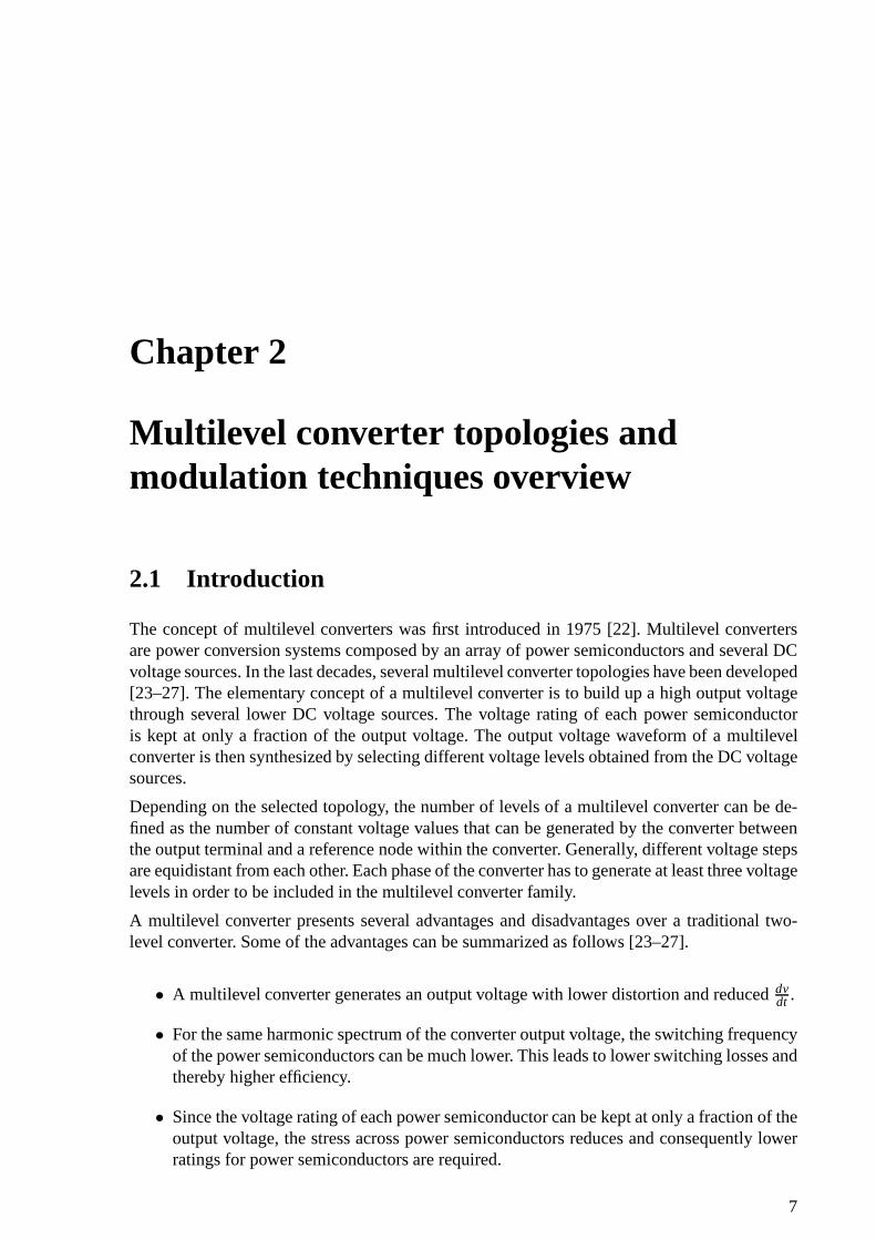
Modularity, in industrial design, refers to an engineeringtechnique that builds large systems bycombining smaller and identical subsystems. Designing power converter using the modularityconcept was first introduced by Marchesoni et al., in 1990 [37]. The modular configurationsconsist of many identical cells connected in series. These cells can be either half- or full-bridge(H-bridge) converter. Figure 2.5 shows the half- and full-bridge cells with switching states andcorresponding output voltage levels.
Different modular configurations will be shown in Section 2.3 but for illustration purpose, asingle-line diagram of a five-level star configuration is shown in Fig. 2.6. This topology is capa-ble of reaching high output voltage levels using only standard low-voltage technology compo-nents. Due to the modularity, in case of a fault in one cell, itis possible to replace it quickly andeasily. Moreover, it is possible to bypass the faulty modulewithout stopping the load, bringingan almost continuous overall availability.
Although modular configurations presents a fairly simple structure, they suffer from require-ment of large number of cells (more isolated capacitors) to decrease the harmonics and swit-ching frequency. This leads to a more complex DC-voltage regulation loop. However variouscontrol algorithms exist to control high number of capacitors voltage [8]. Moreover, due tothe lack of a common DC link, the output power will be affectedby an oscillatory componenthaving characteristic frequency equal to twice the grid frequency; these oscillations will be ref-lected on the DC-link voltage and therefore each cell necessitates over-sizing of the DC linkcapacitors to provide filtering effect.
13
Chapter 2. Multilevel converter topologies and modulationtechniques overview
x
x
y
)0,1(),( yx gg
)0,0(),( yx gg
)1,1(),( yx gg
y
)1,0(),( yx gg
xyvxyv xyv
dcV
dcV
xg
x
_
g
yg
y
_
g
dcV+
-
xg
x
_
g
yg
y
_
g
dcV+
-x y
xg
x
_
g
yg
y
_
g
dcV+
-
x y
xg
x
_
g
yg
y
_
g
dcV+
-
(a)
n
1xg 0xg
xnvxnv
dcV
x
xg
x
_
g
dcV+
-
xg
x
_
g
dcV+
-
nx
(b)
Fig. 2.5 Cell with switching states and corresponding output voltage level; (a): H-bridge; (b): half-bridge.
It is also possible to use cells with unequal DC source voltages in modular configurations andform an alternative configuration called hybrid or asymmetric configuration [38]. The hybridconfiguration can produce higher voltage level with fewer power electronic requirements. Thisreduces the size and cost when compared to the traditional modular configuration with equalDC-links, since fewer semiconductors and capacitors are employed. The main disadvantage of
14

2.2. Main multilevel converter topologies
x1g
x1
_
g
y1g
y1
_
g
x2g
x2
_
g
y2g
y2
_
g
dcV+
-
dcV+-
Fig. 2.6 Single-line diagram of a five-level star configuration.
this approach is that the converter is no longer modular.
2.2.4 Multilevel converter topologies comparison for STATCOM applica-tions
In recent years, the demand for high-voltage conversion applications has drastically increased.Reliability, availability, controllability, modularity, number of components and losses are themain features for high power STATCOM applications.
In STATCOM applications the converter voltage is increasedthrough a step-up transformerbefore connecting to the grid. Consequently, the current will be high in the low voltage sidewhich leads to higher power loss and thus reduced efficiency.This is the driving force that hasled the research community to focus on transform-less solutions, in order to directly connect theconverter to the grid. In addition, a transformer-less topology allows a reduced footprint for thesystem and a reduction in losses. Since in high-voltage applications the voltage rating usuallyranges several tens to hundreds of kVs, the power processingcannot be accomplished withany single IGBT or similar switch. One way to reach high voltage rating is to connect severalswitches in series and operate them simultaneously. However, the series operation of switchesis very difficult because of tolerances in their characteristics and/or the unavoidable mismatchbetween the driving circuits. The main problem is to ensure an equal voltage sharing among thecomponents during static and dynamic transient states. Furthermore, special arrangements areneeded to guarantee a continuous operation of the device in case of faulty switch.
A simpler method to increase the voltage rating is to use modular configurations. In theseconfigurations the total output voltage of the converter canbe increased by increasing the num-ber of cells, each operated at low voltage. As mentioned before it is possible to raise the voltagein modular configurations only by increasing the number of voltage levels. The ability of theseconfigurations to increase the number of levels also resultsin better harmonic performance and
15

Chapter 2. Multilevel converter topologies and modulationtechniques overview
lower switching losses. These configurations also have the ability to successfully balance thecapacitor voltages for high number of levels. It is for thesereasons that the modular configu-rations are often considered as the most suitable solution to implement high-power STATCOM,while NPC and CCC are more suitable for medium-voltage and low-power applications. Ta-ble 2.1 summarizes different characteristics of multilevel converter topologies discussed in thissection.
The main modular configurations are the star, delta and double star. In this thesis, the modularmultilevel converters that are based on the use of H-bridge converters will be denoted as Cas-caded H-Bridge (CHB) converters, while the converter basedon half-bridge cells will be simplydenoted as Modular Multilevel Converters (MMCs). Therefore, the star and delta configurationswill be CHB converters, while the double start can be either CHB or MMC depending of theadopted cell topology. Each of these configurations has specific characteristics, advantages anddisadvantages. A detailed review of these configurations isprovided in the next section.
TABLE 2.1. SUMMERY OF MULTILEVEL CONVERTERS CHARACTERISTICS
structure NPC CCC CHBSwitches per phase 2(m−1) 2(m−1) 2(m−1)(Converter with m- level)Clamping diodes per phase(m−1)(m−2) 0 0(Converter with m-level)Capacitors per phase (m−1) (m−1)(m−2)/2 (m−1)/2(Converter with m-level) +(m−1)Loss distribution Uniform Uniform Uniform
with ANPCMaximum practical levels 3-5 levels 5-7 levels No theoretical
limitAvailability Low Low HighModularity No No YesCapacitor sizing low high highCommon DC source Yes Yes NoLow switching Capable Capable with Capable with
large capacitors large capacitors
2.3 Modular subset configurations and comparison
The main modular configurations: star, delta and double starconfigurations [19] are investigatedin this section and their application for STATCOM is addressed.
Star and delta configurations are shown in Fig. 2.7 for the application of three-phase STATCOM.Each phase consists of several H-bridge converters connected in series. Three phases can beconnected in either star (Y , Fig. 2.7(a)) or delta (∆, Fig. 2.7(b)). A prototype of star and deltaconfigurations as three-phase STATCOM was first demonstrated by Peng et al., in 1996 [39].In less than two years, in 1998, GEC ALSTHOM T&D (now ALSTOM T&D) proposed to use
16

2.3. Modular subset configurations and comparison
(a)
~
(b)
Fig. 2.7 CHB configurations; (a): star configuration; (b): delta configuration.
these configurations as a main power converter in their STATCOMs. Robicon Corporation alsocommercialized their medium voltage drives utilizing these configurations in 1999. Currentlythese devices offer a power range of 10-250 MVAr [40, Chapter2].
Another modular configuration that is receiving increased research focus is the MMC, whichwas first introduced by Marquardt and Lesincar in 2003 [9]. This configuration is shown inFig. 2.8. Each phase of the converter, also called converterleg, consists of two arms. Each armcontains equal number of cells and a coupling inductor to limit the current under AC fault andalso to limit thedi/
dt due to switching. The AC output is connected in the middle of the twoarms. It is also possible to use H-bridge instead of half-bridge as illustrated in Fig. 2.9.
Comparing the star and delta configurations, the first difference is in their voltage and currentrating. Under balanced grid voltage condition with equal number of cells per phase and similarpower electronic equipment, star has
√3 time higher current rating compared to the delta, while
delta has√
3 time higher voltage rating compared to the star in each phase. In case of unba-lanced grid voltage, delta has the ability to exchange negative-sequence current with the grid bycontrolling a zero-sequence current that circulates inside the∆. Although it leads to a slight in-crease in losses, the circulating current can exchange power between phases, which can be usedto balance capacitor voltages especially when negative-sequence reactive power is needed.Thisalso results in an increased current rating as compared to balance condition (and consequentlyhigher current rating compared to the star). Higher currentrating not only affects the rating ofthe semiconductors in the bridges, but more importantly affects the current ripple, and therebythe rating of the capacitors in each bridge. With the same reasoning, the star configuration needsto be over-rated in terms of voltage when operated under unbalanced grids, due to the needed
17
Chapter 2. Multilevel converter topologies and modulationtechniques overview
2Upper arm voltage
2Lower arm voltage
AC output voltage
(Upper-Lower)/2
Neutral point of upper arm
(forth terminal)
Nutral point of lower arm
(Fifth terminal)
upper arm
Lower arm
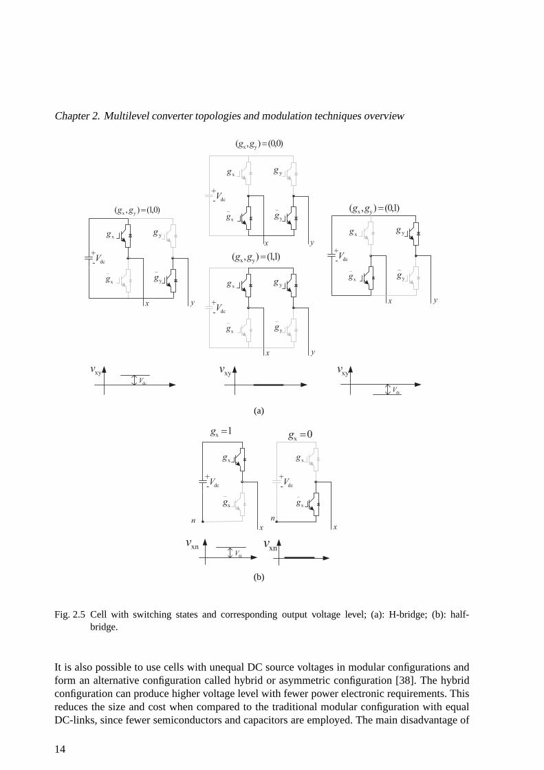
Fig. 2.8 Double star configuration with half-bridge cells (known as MMC).
zero-sequence voltage (which will lead to a movement of the floatingY -point of the converter)to guarantee capacitor voltage balancing.
Regarding the double-star configurations, CHB and MMC are ”five-terminal circuits” becausetwo neutral points of upper and lower arms are used as the two DC terminals. This is the mainadvantage of these configurations over star and delta since they can manipulate active powerwithout the need of isolated DC sources in each cell. This is particularly important in High Vol-tage DC (HVDC) and motor drive applications, where large amount of active power is transfer.However, being the focus of this thesis on STATCOM applications only, a common DC-linkbetween the three phases is not needed.
In STATCOM application the converter must be able to providereactive power under unba-lanced condition. Double star configurations, similar to the delta, have the ability to exchangenegative-sequence current with the grid by controlling thecirculating current.
One of the other important feature of the double-star configuration is the lower device currentrating of the individual cells, due to the AC current sharingbetween the two converter arms.
18

2.3. Modular subset configurations and comparison
Fig. 2.9 Double star with CHB configuration.
However, the voltage rating of these devices is higher compare with the star and delta. Asit is shown in Fig. 2.8 each converter arm generates an AC voltage with a DC offset equalto half of the total DC-link voltage in MMC. This results in a higher converter arm voltagerating (two times the AC voltage). If H-bridge cells are usedinstead of half-bridge cells, eacharm is needed to generate only the AC voltage with the same amplitude of the output voltage.Therefore the number of cells reduces to half as compare withthe double star with half-bridgewhile the number of power semiconductor in each cell is now doubled. As an example if half-and H-bridge cells with 1pu voltage rating are available, inorder to generate an AC voltagewith 1pu peak under balanced conditions, only one cell per phase is needed if star configurationis chosen while
√3 cells are needed for delta. Double star configuration with half-bridge cells
needs 4 half-bridge cells and double star configuration withH-bridge cells needs 2 H-bridgecells to satisfy the requirements.
The interaction between DC offset voltage at each arm and fundamental current in double starconfiguration results in a large fundamental frequency component in the arm capacitor voltages.This increases the capacitor voltage ripple as compared with the star and delta configurations.Thus the size of the capacitors and hence cost and footprintsincrease significantly in the doublestar configuration.
19

Chapter 2. Multilevel converter topologies and modulationtechniques overview
Double star configuration with H-bridge cells is superior tothe one with half-bridge cells sinceit has additional buck and boost functions of the DC-link voltage. Having H-bridge cells en-ables this configuration to tolerate a broad range of variation in the DC-link voltage.This fea-ture makes it suitable for renewable resources such as wind and solar power since the DC-linkvoltage varies with weather variations. Moreover, this configuration has the ability to suppressfault currents arising from DC-side short circuit events [41].
In STATCOM applications, where only reactive power is exchanged with the grid, star and deltaconfigurations have superior performances. Besides havinga less complex controller they havehigher efficiency, need less number of cells [42] and have better dynamic performance [28].Table 2.2 summarizes different characteristics of all modular subset configurations discussedin this chapter.
This section introduces the main modular configurations. Several alternative modular configu-rations can be found in literature [43,44].
TABLE 2.2. SUMMERY OF MODULAR SUBSET CONFIGURATIONS CHARACTERISTICS
star delta double star double starMMC CHB
Cell numbers vac/
Vdc
√3vac
/
Vdc4vac
/
Vdc2vac
/
Vdcbalanced condition
current rating√
3/phase 1/phase 0.5/phase 0.5/phasebalanced condition
Negative-sequence capable (v0) Capable(i0) Capable(i0) Capable(i0)compensation
Circulating current No Yes Yes Yes
Voltage rating Balanced No change No change No changeunbalanced condition voltage+v0
Current rating No change Balanced Balanced Balancedunbalanced condition current+i0 current+i0 current+i0
Capacitor size Higher than - Higher than Higher thanbalanced condition delta star&delta star&delta
Capacitor size Lower than - Higher than Higher thanunbalanced condition delta star&delta star&delta
Hardware complexity Lowest - - -
Controller complexity Medium Medium High High
Cost capacitor & switch trade off
20

2.4. Multilevel converter modulation techniques
Multilevel modulation techniques
Multicarrier PWMHybrid PWMFundamental
switching frequencySVM
NVCNLC PS-PWM LS-PWM
PD-PWMPOD-PWM APOD-PWM
SHE
Fig. 2.10 Multilevel converter modulation techniques.
2.4 Multilevel converter modulation techniques
A modulation technique determines the switching function of a converter. The modulation tech-nique must guarantee that the generated voltage at the output of the converter is similar to the de-sired voltage as much as possible. The challenge is to extendtraditional modulation techniquesto the multilevel case, where the large number of cells givesdifferent alternatives to modulatethe converter. Each modulation approach focuses on the optimization of some converter featuressuch as switching loss reduction, uniform switching loss distribution, improving harmonic per-formances, common-mode voltage minimization, minimum computational cost, etc. The mostcommon modulation techniques for multilevel converters are summarized in Fig. 2.10.
The fundamental switching modulators, provide a switchingfunction such that each cell hasonly one commutation per fundamental cycle. The switching function with multicarrier PWMare determined based on comparison between carriers and a reference signal. Hybrid PWMis a mixture of fundamental and carrier-based modulation. Space Vector Modulation (SVM)considers all the possible switching states and select the best combinations in each control cycleto generate an output voltage with equal volt/second as the reference value. Detail descriptionof each modulator is provided in this section.
It is also worth mentioning that the switching commands for the converter are not always deter-mined by a dedicated modulation stage; instead, they can be determined by a direct consequenceof the overall converter controller. Hysteresis current controller and Model Predictive Control(MPC) are typical examples of these type of controllers.
2.4.1 Multicarrier PWM
1. Phase−Shi f ted PWM (PS−PWM): This method is a natural extension of the traditionalbipolar and unipolar PWM techniques. This modulation technique is one of the mostcommonly used modulation techniques for multilevel converters with half or H-bridge
21
Chapter 2. Multilevel converter topologies and modulationtechniques overview
cells, such as CCC and all the modular configurations.
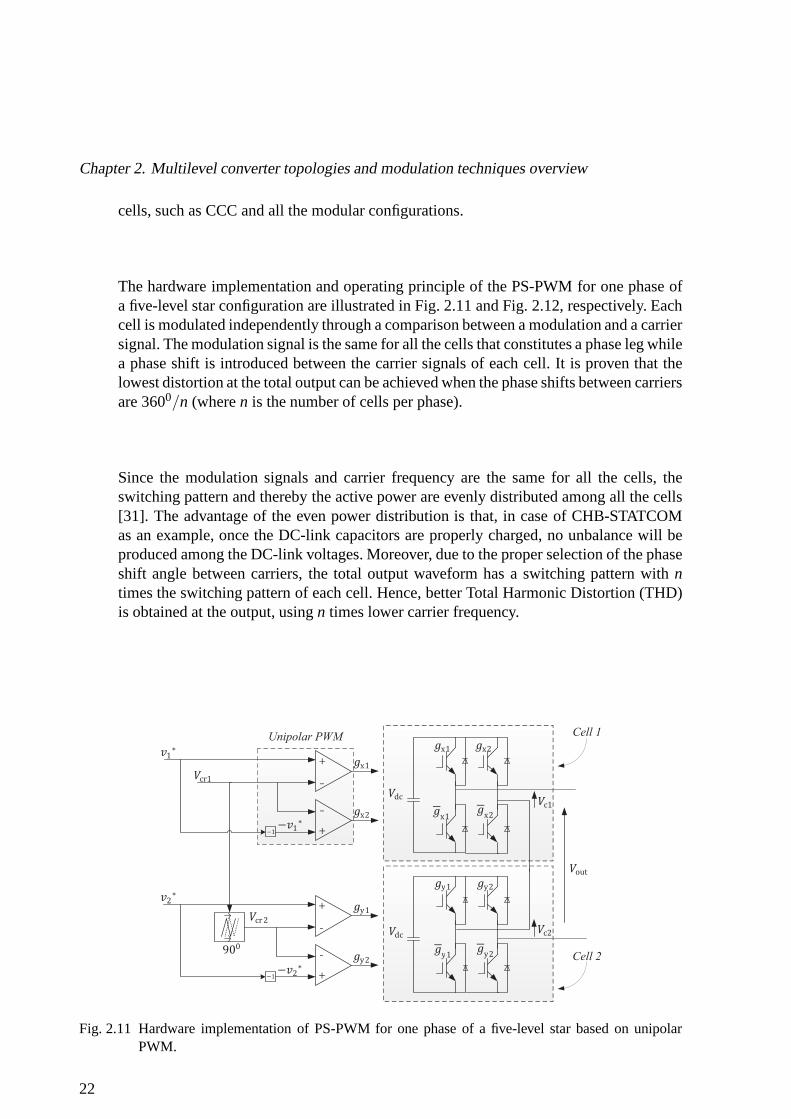
The hardware implementation and operating principle of thePS-PWM for one phase ofa five-level star configuration are illustrated in Fig. 2.11 and Fig. 2.12, respectively. Eachcell is modulated independently through a comparison between a modulation and a carriersignal. The modulation signal is the same for all the cells that constitutes a phase leg whilea phase shift is introduced between the carrier signals of each cell. It is proven that thelowest distortion at the total output can be achieved when the phase shifts between carriersare 3600/n (wheren is the number of cells per phase).
Since the modulation signals and carrier frequency are the same for all the cells, theswitching pattern and thereby the active power are evenly distributed among all the cells[31]. The advantage of the even power distribution is that, in case of CHB-STATCOMas an example, once the DC-link capacitors are properly charged, no unbalance will beproduced among the DC-link voltages. Moreover, due to the proper selection of the phaseshift angle between carriers, the total output waveform hasa switching pattern withntimes the switching pattern of each cell. Hence, better Total Harmonic Distortion (THD)is obtained at the output, usingn times lower carrier frequency.
_
_
Unipolar PWM
_
_
Cell 1
Cell 2
Fig. 2.11 Hardware implementation of PS-PWM for one phase ofa five-level star based on unipolarPWM.
22

2.4. Multilevel converter modulation techniques
0 0.002 0.004 0.006 0.008 0.01 0.012 0.014 0.016 0.018 0.02−1
0
1
cell 1 o
utpu
t
volta
ge [p
u]
V
cr1
Vc1
v1*
0 0.002 0.004 0.006 0.008 0.01 0.012 0.014 0.016 0.018 0.02−1
0
1
cell 2 o
utpu
t
volta
ge [p
u]
V
cr2
Vc2
v2*
0 0.002 0.004 0.006 0.008 0.01 0.012 0.014 0.016 0.018 0.02−1
0
1
carr
ier
sign
als
V
cr1
Vcr2
0 0.002 0.004 0.006 0.008 0.01 0.012 0.014 0.016 0.018 0.02−2
0
2
conv
erte
r ou
tput
volta
ge [p
u]
V
out
v*
Fig. 2.12 Operating principle and switching pattern of the PS-PWM based on unipolar PWM.
2. Level − Shi f ted PWM (LS −PWM): This method is a natural extension of traditionalbipolar PWM techniques. In traditional bipolar PWM, a carrier signal is compared withthe reference to decide between two different voltage levels. If the reference voltage isgreater than the carrier then a switching command that generates the positive voltagelevel is sent to the converter. In another case, if the reference is less than the carrier, aswitching command that generates the negative voltage level is sent to the converter.
By extending this idea for a multilevel converter withm levels,m−1 carriers are needed.Each carrier is set between two voltage levels and the same principle of bipolar PWM isapplied. Required carriers can be arranged in vertical shifts. If all the carriers are in phasewith each other (only vertical shift), the modulation technique is named Phase Disposi-tion PWM (PD-PWM). If all the positive carriers in phase witheach other and in oppositephase of the negative carriers, we talk about Phase Opposition Disposition PWM (POD-PWM). By alternating the phase between adjacent carriers, Alternate Phase OppositionDisposition PWM (APOD-PWM) is obtained. Different arrangement of carriers providesdifferent THD. For example POD-PWM at the expense of having more complicated struc-ture than PD-PWM has less THD than PD-PWM [45],[46]. An example of these arrange-ments for a five-level (thus four carriers) star configuration is given in Fig. 2.13. Theswitching command must be wisely directed to the appropriate power semiconductor inorder to generate the corresponding levels. The hardware implementation and cell outputvoltage by using LS-PWM for a five-level star configuration isillustrated in Fig. 2.14.
This modulation technique can be adapted to any multilevel converter. However, as it canbe observed from Fig. 2.15, it is clear that the switching pattern is not uniform betweentwo cells when LS-PWM is used. This causes an uneven power distribution among thedifferent cells.
23

Chapter 2. Multilevel converter topologies and modulationtechniques overview
0 0.002 0.004 0.006 0.008 0.01 0.012 0.014 0.016 0.018 0.02−2
0
2(a)
conv
erte
r ou
tput
volta
ge [p
u]
0 0.002 0.004 0.006 0.008 0.01 0.012 0.014 0.016 0.018 0.02−2
0
2(b)
conv
erte
r ou
tput
volta
ge [p
u]
0 0.002 0.004 0.006 0.008 0.01 0.012 0.014 0.016 0.018 0.02−2
0
2(c)
conv
erte
r ou
tput
volta
ge [p
u]
Vcr1
Vcr2
Vcr3
Vcr4
Vref
Fig. 2.13 LS-PWM arrangement; (a): PD; (b): POD; (c): APOD.
_
_
Cell 1
Cell 2
_
_
Fig. 2.14 Hardware implementation of LS-PWM.
24

2.4. Multilevel converter modulation techniques
0 0.002 0.004 0.006 0.008 0.01 0.012 0.014 0.016 0.018 0.02−1
−0.5
0
0.5
1
cell
1 ou
tput
volta
ge [p
u]
0 0.002 0.004 0.006 0.008 0.01 0.012 0.014 0.016 0.018 0.02−1
−0.5
0
0.5
1
cell
2 ou
tput
volta
ge [p
u]
Fig. 2.15 Cell output voltages by using LS-PWM.
2.4.2 Space Vector Modulation (SVM)
Using Fig. 2.16 (a) different steps of SVM can be summarized as follow. First step is to deter-mine all the switching states and their corresponding state-space vector inαβ -reference frame.Fig. 2.16 (a) shows all the eight switching space vectors with black circles for a traditionaltwo level converter. + and - signs in parentheses are to show which switch in each phase is on.For example(−,+,+) shows that in phasea lower switch and in the other two phases upperswitches are on.
Second step is to determine the reference voltage state-space vector inαβ -reference frame.Third step is to find the three closest switching combinationto the reference (v1,v2,v3 inFig. 2.16 (a)). The final step is to calculate the time duration of each switching state (t1, t2)so that the time average of the generated voltage equals the reference space vector.
Figure 2.16 (b) shows the extension of SVM for a three level star (one cell per phase). Eachcell can produce positive (+Vdc), negative (−Vdc) and zero (0) voltage levels. Having 3 levels,results in 33 possible combinations, shown with black circles. It can be observed that for somevectors more than one switching state is possible.
Following the same steps as explained beforev1,v2,v3 and their corresponding timet1, t2, t3should be determined in order to make the switching commands.
It should be noted that SVM explained here is valid only for a balanced system with purelysinusoidal reference voltages. In case of an unbalanced system, existence of harmonics or zero-sequence component this algorithm must be modified [47,48].
25

Chapter 2. Multilevel converter topologies and modulationtechniques overview
(-,-,-)
(+,+,+)
(0,0,0)
(+,0,0)
(0,-,-) (+,-,-)(0,+,+)
(-,0,0)(-,+,+)
(0,0,+)
(-,-,0)
(+,0,+)
(0,-,0)(+,-,0)
(+,-,+)
(0,-,+)(-,-,+)
(-,0,+)
(+,0,-)(+,+,0)
(0,0,-)(0,+,0)
(-,0,-)(-,+,0)
(-,+,-)
(0,+,-)
(+,+,-)
(-,-,-)
(+,+,+)
(+,-,-)(-,+,+)
(-,-,+) (+,-,+)
(+,+,-)(-,+,-)
(a) (b)
Fig. 2.16 SVM principle for; (a): traditional two level converter; (b): three-phase three-level star configu-ration.
2.4.3 Fundamental switching modulators
1. Selective Harmonic Elimination (SHE): The basic idea of SHE is predefining and pre-calculating switching angles per quarter-fundamental cycle via Fourier analysis to ensurethe elimination of undesired low-order harmonics. The firststep is to find the Fourier se-ries of the multilevel waveform based on unknown switching angles. Next step is to setthe undesired Fourier coefficient to zero, while the fundamental component is made equalto the desired reference value. The obtained equations are solved offline using numericalmethods, finding solution for the angles.
As an example for phasea of the star configuration with three H-bridges per phase, a typi-cal waveform considering three switching angles(α1,α2,α3) is given in Fig. 2.17. Eachangle is associated to a particular cell. Consequently eachcell of the converter producespositive or negative voltage levels at a specific angle only once in a fundamental cycle.SHE is also known as staircase modulation because of the stair-like shape of the voltagewaveform.
Note that there is no control over non eliminated harmonics and if non eliminated har-monic amplitude are not suitable for a particular application, additional cells and anglescan be introduced. It is also possible to limit the harmonic content to acceptable values
26

2.4. Multilevel converter modulation techniques
3
-3
-
-
-
Ce
ll 1
ou
tpu
t
Vo
lta
ge
[p
u]
Ce
ll 2
ou
tpu
t
Vo
lta
ge
[p
u]
Ce
ll 3
ou
tpu
t
Vo
lta
ge
[p
u]
Co
nve
rte
r o
utp
ut
Vo
lta
ge
[o
u]
Fig. 2.17 SHE technique for phasea of the star configuration with 3 cells per phase.
instead of completely eliminating them. This method is called Selective Harmonic Miti-gation (SHM).
The main advantage of SHE is the reduction of the switching frequency and consequentlythe switching losses. It also eliminates the low order harmonics, facilitating the reductionof output filter size. However, this method requires numerical algorithms to solve theequations for different modulation indexes. With current technology of microprocessorsit is not possible to do the calculations in real time. Therefore, the solutions are storedin a look-up table, and interpolation is used for those unsolved modulation indexes. Thismakes SHE method not suitable for applications where high dynamic performance isneeded.
2. Nearest Vector Control (NVC): NVC also known as State Vector Control is the alterna-tive method to SHE to provide a low switching frequency, withno numerical calculationand poor dynamic performance. The basic idea is to simply approximating the referencevoltage to the closest voltage vectors that can be generatedin theαβ frame.
The dots in Fig. 2.18 shows all the possible voltage vectors generated by the converter,surrounded by the hexagons. Each converter vector is considered as the closest vector tothe reference, as long as the reference voltage is located inside the hexagon surroundedthat vector. Hence, when the reference voltage falls into a certain hexagon, the corres-ponding vector is generated by the converter.
Unlike SHE, this technique does not eliminate low-order harmonics. However, this prob-lem can be avoided by using multilevel converters with a highnumber of levels. High
27

Chapter 2. Multilevel converter topologies and modulationtechniques overview
Fig. 2.18 All the possible voltage vector for a three-level star configuration and their correspondinghexagon.
number of levels provides more available voltage vectors and thereby smaller error. De-spite the simple operating principle, its practical implementation is not trivial.
3. Nearest level Control (NLC): NLC, also known as round method, is somehow the per-phase time domain counterpart of the NVC. The basic principle in both methods is thesame but instead of choosing the closest vector, when using NLC the voltage level closestto the reference voltage is selected. Also unlike NVC, wherethree phases are controlledsimultaneously with the vector selection, here three phases are controlled independentlywith 1200 phase shifted references. The main advantage of this methodover NVC isthat since finding the closest level is much easier than finding the closest vector to thereference, NLC is greatly simplified in relation to NVC.
The output voltage using NLC is shown in Fig. 2.19 for the firstquarter cycle of thereference voltage, whereVdc is the voltage difference between two voltage levels (usuallythe DC-link voltage in modular configurations),v∗ is the reference voltage andVout is theoutput voltage. As can be seen from Fig. 2.19 the maximum error in approximation of theclosest voltage level isVdc
/
2.
Similar to NVC, NLC does not eliminate specific low-order harmonics. Therefore, both
28

2.5. Conclusion
Fig. 2.19 The output voltage waveform using NLC.
NVC and NLC are not recommended for multilevel converters with reduced number oflevels. Hence these methods are more suitable for converters with higher number of le-vels to avoid important low-order harmonics. The main advantages of NLC over otherswitching techniques is its simplicity in both implementation and concept, and efficiencyimprovement due to the low switching frequency.
2.4.4 Hybrid PWM (H-PWM)
This modulation technique is an extension of PWM for hybrid or asymmetric configuration(modular configurations with unequal DC sources). The basicidea of this modulation techniqueis to reduce the switching losses and improve the converter efficiency by reducing the switchingfrequency of the higher power cells. To do this, instead of using high-frequency carrier-basePWM for all cells, high power cells can be controlled at a fundamental switching frequency,while the low-power cells are controlled by using unipolar PWM. Detail description of thismodulation technique can be found in [31].
The modulation techniques introduced in this chapter are based on having fixed DC sourcesas DC-links in multilevel converters. In the field of STATCOM, DC sources are replaced bycapacitors. This is an important parameter that has to be taken into account when using anyof the modulation techniques introduced in this chapter. More details about modification ofthe modulation techniques considering having capacitors as DC sources will be provided inChapter 4.
2.5 Conclusion
Multilevel converters have become an attractive solution for high power applications. The mostcommon multilevel converter topologies have been described in this chapter. Complexity bothin control and hardware structure, reliability, modularity and efficiency as the most importantparameters for high power applications are addressed for the described topologies. Severalmodulation techniques for multilevel converters were alsobriefly reviewed.
29

Chapter 2. Multilevel converter topologies and modulationtechniques overview
30

Chapter 3
Overall control of CHB-STATCOM
3.1 Introduction
CHB configurations (star and delta) present outstanding advantages as modularity, high powerand high voltage capability using low rated components as compare with the other multileveltopologies. Nevertheless, these salient features requireelaborated and not trivial control strate-gies due to the complexity of these configurations.
Control objectives of CHB-STATCOMs can be classified into two main categories: controllingthe exchanging current and thereby the exchanging power between the converter and the grid,and ensure the capacitor voltage balancing among all cells.Several linear and non-linear ap-proaches have been proposed for modular configuration basedSTATCOMs [49]. The simplestcontrol strategy is based on linear PI controller implemented in the rotatingdq-reference frame[8]. This method requires a robust synchronization method to transform AC quantities to DC.
It is also possible to directly control the AC quantities with a fast dynamic. This controller isbased on instantaneous power theory inαβ - or three-phase system. The main advantage of thiscontrol strategy is that no synchronous transformation is needed. The simplest linear approach toimplement this control strategy is the Proportional Resonant (PR) controller [50]. However, thiscontroller has the restriction of constant frequency operation. Two main non-linear approachesto implement the controller for CHB-STATCOMs are hysteresis control [51] and MPC [52].The main drawback of MPC when applied to CHBs with high numberof levels is the highnumber of switching states that must be evaluated.
It is not easy to define which one of the control strategies achieves the best results. But itmust be noted that computational burden is as important factor as the dynamic and steady statebehaviors of the control strategy. Considering the actual devices for control purposes such asDigital Signal Processing (DSP) and Field Programmable Gate Array (FPGA), to implement anadvanced control algorithm put a heavy restriction in choosing the control algorithm.
In this chapter the overall control of CHB-STATCOMs implemented in the rotatingdq-referenceframe is provided. Due to its uniform switching pattern and thus uniform power distributionamong cells, PS-PWM is here considered as the modulator stage.
31

Chapter 3. Overall control of CHB-STATCOM
3.2 CHB-STATCOM modeling and control
3.2.1 System modeling
In order to be able to derive an adequate control algorithm, first the dynamic and steady-statemodeling equations of the CHB-STATCOM should be defined. Through steady-state analysis, itis possible to calculate the reference voltages required toreach an arbitrary operating condition.This is especially useful to determine the capabilities of CHB-STATCOM through an open loopcontrol. The CHB-STATCOMs with an arbitrary number of cellsn per phase is shown in Fig. 3.1and Fig. 3.2 in its star and delta configurations, respectively.
The voltage difference between grid and converter output voltages is supported by a passive fil-ter in each phase, used to filter the harmonics in the injectedcurrent. For the delta configurationthe filter is typically connected inside the delta; in this way the filter can handle the voltagedifference between converter phases and limit the circulating current inside the delta.
The dynamic model of the system in Fig. 3.1 can be obtained using Kirchhoff’s circuit law. Inthis analysis it is assumed that all the cells have equal DC-link capacitor, charged at the samevoltage level; also, it is assumed that the AC voltage is equally shared among all the cells. Theset of voltage-current equations on the AC side can be obtained as
LfdiaYdt +RfiaY+ ea = nsa
cvdc
LfdibYdt +RfibY + eb = nsb
cvdc
LfdicYdt +RficY + ec = nsc
cvdc
(3.1)
where,sac,s
bc andsc
c are the switching functions of the different cells in phasea,b andc (which canbe+1,−1 and 0).Rf andLf are the resistance and inductance of the filter reactor, respectively.nis the number of cells per phase andvdc is the DC-link voltage of the cells. Using the exchangingactive power between the grid and the converter, the dynamicequation of the DC side for onecell (for example in phasea) is obtained as
p =dwdt
=12
Cdcd(v2
dc)
dt=
pa− Rf |iaY|22
n− v2
dc
Rdc(3.2)
wherew and p are the energy stored in the DC-link capacitor and the activepower flows inthe cells respectively.Cdc is cell capacitor andRdc is an additional resistor connected in parallelto the capacitor (not displayed in Fig. 3.1 and 3.2 for clarity of the figures) and represents theoverall losses in the DC side;pa is the active power absorbed from the grid in phase lega. It isimportant to remark that (3.2) can be easily extended to the other two phases.
In order to simplify the dynamic equations, the switching functions are replaced with theirfundamental component. The fundamental component is called modulation signal. For examplefor phasea
32

3.2. CHB-STATCOM modeling and control
phase bphase a phase c
H-Bridge
H-BridgeH-Bridge
H-BridgeH-Bridge
H-Bridge
Point of common coupling
Rf, Lf
Fig. 3.1 Star configuration.
H-Bridge
H-Bridge
phase a phase cphase b
H-BridgeH-Bridge
H-BridgeH-Bridge
Point of common coupling
Rf, Lf
Fig. 3.2 Delta configuration.
33

Chapter 3. Overall control of CHB-STATCOM
sac∼= ma
c (3.3)
wheremac is the modulation signal for one cell in phasea.
Replacing (3.3) into (3.1) and applying Clarke transformation (described in the Appendix), thedynamic equation in the fixedαβ -frame can be written as
nmαβ (t)vdc− eαβ (t)−RfiYαβ(t)−Lf
ddt
iYαβ(t) = 0 (3.4)
Having the transformation angleθ (the angle of the grid voltage vector) and using Park trans-formation (in Appendix) as
mdq(t) = mαβ (t)e−jθ (t)
edq(t) = eαβ (t)e−jθ (t)
iYdq(t) = iY
αβ(t)e−jθ (t)
(3.5)
(3.4) can be re-written in the rotatingdq-reference frame as
nmdq(t)vdc− edq(t)−RfiYdq(t)−Lf
ddt
iYdq(t)−Lf jωiY
dq(t) = 0 (3.6)
Re-arranging (3.2), the resulting dynamic equations indq-frame are given by
Lfddt idq(t)+Rfidq(t)+ edq(t)+ jωLfidq(t) = nmdq(t)vdc
12Cdc
d(v2dc)
dt =edid+eqiq−Rf(i2d+i2q)
3n − v2dc
Rdc
(3.7)
whereω is the angular frequency of the rotating vectors.
3.2.2 Steady-state analysis
In steady-state condition, the derivative terms are equal to zero. By setting the derivative termsin (3.7) to zero, the steady-state equations are calculatedas
Mdq =RfIdq+Edq+ jωLfIdq
nVdc
0=EdId−RfI2
d3n +
EqIq−Rf I2q
3n − V 2dc
Rdc
(3.8)
where the use of capital letters denote the steady-state condition of the different quantities. Inorder to solve this equation,Iq andVdc should be determined first. Usually, the desired value
34

3.2. CHB-STATCOM modeling and control
for Iq is determined based on the required reactive power to be exchanged with the grid. If thedq-reference frame is synchronized with the grid voltage vector, theq component of the voltage(Eq = 0) can be considered equal to zero in steady-state. Thus, thedesired value forIq can becalculated as
Q∗ = ImEdqI∗dq=−EdIq+EqId ⇒ Iq =−Q∗
Ed(3.9)
whereQ∗ is the required reactive power. The DC voltageVdc must be selected to a value thatensures the summation of all cells DC voltages at each phase is higher than the amplitude of thegrid phase voltage, i.e.,
nVDC >
√2√3
√
E2d +E2
q ⇒ VDC|Eq=0 = k
√2Ed√3n
(3.10)
wherek is a safety margin to guarantee proper operation of the converter, also in case of gridvoltage transient; typically,k ranges between 1.1 and 1.15 [40].
ReplacingVdc andIq in (3.8), the needed modulation signal corresponding to thespecific ope-rating condition can be calculated.
Just for illustration purposes, the following desired steady-state values in per unit and securitymargin of 15% for the DC-link voltage are here considered. The resulting modulation signalscan be calculated as
n = 3
Ed = 1pu⇒VDC = 0.313pu
Iq =−1pu
Lfω = 0.15pu
Rf = 0.03pu
Rdc = 30pu
⟩⟨Md = 0.9
Mq =−0.03pu
Id∼= 0pu
(3.11)
According to the calculated modulation signals, the safetymargin of 15% ensures the properoperation of the converter without any over-modulation.
3.2.3 Control design and algorithm
The control method used for the CHB-STATCOMs consists of an inner current control loop,which is used to control the converter output current, and anouter cluster controller, used tocontrol the DC capacitor voltages in each phase. Figure 3.3 shows the block diagram of the
35
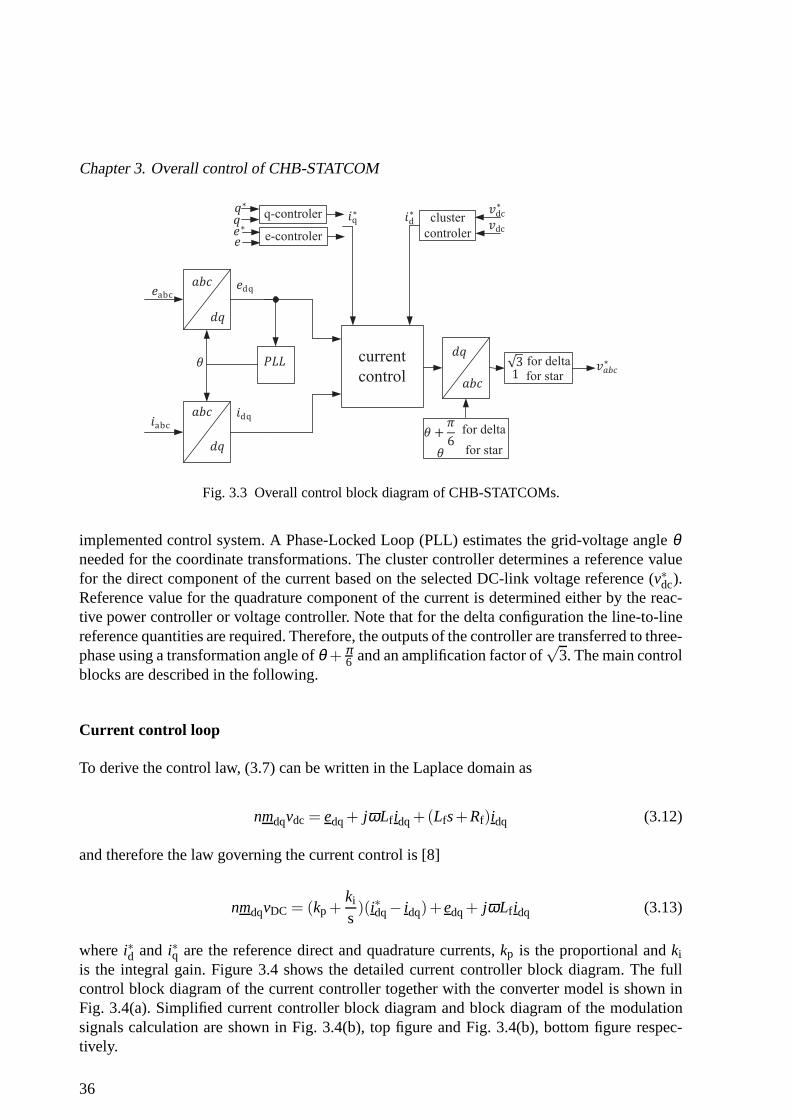
Chapter 3. Overall control of CHB-STATCOM
cluster
controler
current
control
for delta
for star
for delta
for star
q-controler
e-controler
Fig. 3.3 Overall control block diagram of CHB-STATCOMs.
implemented control system. A Phase-Locked Loop (PLL) estimates the grid-voltage angleθneeded for the coordinate transformations. The cluster controller determines a reference valuefor the direct component of the current based on the selectedDC-link voltage reference (v∗dc).Reference value for the quadrature component of the currentis determined either by the reac-tive power controller or voltage controller. Note that for the delta configuration the line-to-linereference quantities are required. Therefore, the outputsof the controller are transferred to three-phase using a transformation angle ofθ + π
6 and an amplification factor of√
3. The main controlblocks are described in the following.
Current control loop
To derive the control law, (3.7) can be written in the Laplacedomain as
nmdqvdc = edq+ jωLf idq+(Lfs+Rf)idq (3.12)
and therefore the law governing the current control is [8]
nmdqvDC = (kp+ki
s)(i∗dq− idq)+ edq+ jωLf idq (3.13)
wherei∗d and i∗q are the reference direct and quadrature currents,kp is the proportional andkiis the integral gain. Figure 3.4 shows the detailed current controller block diagram. The fullcontrol block diagram of the current controller together with the converter model is shown inFig. 3.4(a). Simplified current controller block diagram and block diagram of the modulationsignals calculation are shown in Fig. 3.4(b), top figure and Fig. 3.4(b), bottom figure respec-tively.
36

3.2. CHB-STATCOM modeling and control
The proportional and integral gains of the implemented controller can be easily found shapingthe closed-loop transfer function to have the same responseas a first-order low-pass filter ofbandwidthαi , i.e.
Gi =i∗dq
idq=
skp+ ki
Lfs2+ s(Rf + kp)+ ki=
αi
s+αi(3.14)
Therefore, the proportional and integral gains can be foundas
kp = αiLfki = αiRf
(3.15)
Note that (3.12), (3.13), (3.14) and (3.15) are obtained forthe star configuration. Consideringthe same filter impedances in each phase leg, the same equations can be written for the deltaconfiguration except that one third of the actual value of theLf andRf should be considered.The ratio of one third is the delta to star impedance transformation.
Outputs of the current controller are direct and quadraturecomponents of the reference voltagevector. In order to provide the modulation signal for each cell, the reference-voltage vectorshould be transferred to three-phase and normalized by the DC-link voltages. This is shownin Fig. 3.4(b) (bottom) whereva
dc1,...,vadcn are the DC-link voltage values andma
c1 ,..., macn are
the modulation signals of the cells in phasea. With the same algorithm, modulation signals forthe cells in other two phases can be obtained. These modulation signals are then sent to themodulator (for example, PS-PWM) to determine the switchingpatterns for the cells.
Converter model
feed forward
feed forward
Coupled terms
(a)
current
controller
.
.
.
,
(b)
Fig. 3.4 Current control block diagram; (a): full-controller; (b-top): simplified controller; (b-bottom):cells modulation signal.
37

Chapter 3. Overall control of CHB-STATCOM
~
Fig. 3.5 Equivalent circuit of the star configuration for phasea.
Cluster control
The aim of the cluster controller is to generate the requiredreference direct-component of thecurrent.
The equivalent circuit of the star configuration is shown in Fig. 3.5 for phasea. The DC capaci-tors are considered to be all in series. Assuming a loss-lesssystem, the active power on the ACand on the DC side of the converter can be written as
pdc =dwdt
=12
Cdc
nddt(va
dc1+ vadc2+ ...+ va
dcn)2 =
n2
Cdcddt(va
dc1+ vadc2+ ...+ va
dcn
n)2 =
=n2
Cdcddt(vcla)
2
pac=|ea| |iaYd|
2
(3.16)
wherevcla is calledcluster voltage of phasea and is the average voltage of all the DC-linkvoltages in phasea. The active component of the three-phase current denoted byiaYd for phasea, has the same phase angle of the grid voltage. Being the AC andDC side active powers equal,(3.16) can be written in Laplace domain as
nCdcsv2cla = |ea||iaYd| (3.17)
The termiaYd is determined based on the desired DC-link voltage. Using a proportional con-troller having a gain ofkclY, all three phase direct currents can be written as
iaYd= kclY(v∗2dc− v2
cla)cos(θ)
ibYd = kclY(v∗2dc− v2
clb)cos(θ −2π3)
icYd = kclY(v∗2dc− v2
clc)cos(θ +2π3)
(3.18)
where cos(θ) is used to generate AC currents that are in phase with the gridvoltage;v∗dc is theDC-link reference voltage andvcla,vclb,vclc are the cluster voltages in phasea,b,c. The amplitude
38

3.2. CHB-STATCOM modeling and control
of the active current component of phasea from (3.18) can be replaced into (3.17). Simplifyingthe results, the transfer function of the cluster controller for phasea can be calculated as
Gcla=v2
cla
v∗2dc
=kclY|ea|/nCdc
s+ kclY|ea|/nCdc
=αcl
s+αcl(3.19)
which has the same response as a first-order low pass filter of bandwidthαcl. The gainkclY canthen be designed for a desired bandwidthαcl as
kclY =nCdcαcl
|ea|(3.20)
The resulting three-phase currents can then be transferredto the rotatingdq-frame to generatethed-component of the reference current.
Following the same procedure, in order to generate the desired direct component of the currentfor delta configuration, the branch direct currentsia∆d,ib∆d andic∆d must be in phase with theircorresponding line-to-line voltage. Using a proportionalcontroller with gainkcl∆three branchdirect current can be written as
ia∆d = kcl∆(v∗2dc− v2
cla∆)cos(θ + π6)
ib∆d = kcl∆(v∗2dc− v2
clb∆)cos(θ + π6 −2π
3)
ic∆d = kcl∆(v∗2dc− v2
clc∆)cos(θ + π6 +2π
3)
(3.21)
where cos(θ + π6) is to make the branch direct currents in phase with the grid line to line voltage.
The gainkcla∆ can be designed for a desired bandwidthαcl as
kcla∆ =nCdcαcl
|eab|(3.22)
The line direct currentiad,ibd,icd are then calculated from the branch direct currents and theresults are transferred todq-reference frame to generate the desired reference direct current.The block diagram of the cluster controller is shown in Fig. 3.6.
It should be noted that only a proportional controller is chosen for the purpose of capacitorbalancing. This is due to the fact that the DC-link voltages are not necessarily needed to beregulated at a certain voltage and a steady state error in DC-link voltage is acceptable as longas this voltage satisfies the security margin.
3.2.4 Phase-Locked Loop (PLL)
The objective of the PLL is to estimate the angle of the grid-voltage vector to perform thecoordinate transformation. The PLL considered in this thesis is the one proposed in [53],[54].
39
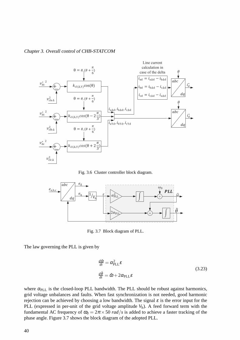
Chapter 3. Overall control of CHB-STATCOM
Line current
calculation in
case of the delta
Fig. 3.6 Cluster controller block diagram.
2 +
+
Fig. 3.7 Block diagram of PLL.
The law governing the PLL is given by
dωdt = α2
PLLε
dθdt = ω +2αPLLε
(3.23)
whereαPLL is the closed-loop PLL bandwidth. The PLL should be robust against harmonics,grid voltage unbalances and faults. When fast synchronization is not needed, good harmonicrejection can be achieved by choosing a low bandwidth. The signalε is the error input for thePLL (expressed in per-unit of the grid voltage amplitudeVb). A feed forward term with thefundamental AC frequency ofω0 = 2π ×50 rad/s is added to achieve a faster tracking of thephase angle. Figure 3.7 shows the block diagram of the adopted PLL.
40

3.2. CHB-STATCOM modeling and control
real
2
conjugate
Fig. 3.8 Block diagram of single phase estimation algorithm.
3.2.5 DC-link filter design
In CHB-STATCOMs, the DC-link voltage of each cell contains aDC and a 100 Hz oscillatorycomponents. The oscillatory component can produce harmfuleffects on the performance of thecontroller. Traditional methods to remove the 100 Hz component are Low-Pass Filter (LPF)and Moving-Average Filter (MAF), which are investigated and applied in [12]. An alternativeway to separate the two frequency components in the measuredDC voltage is to combine aLPF and a resonant filter with characteristic frequency centered at 100 Hz, as described in[55]. The advantage of this approach over the mentioned methods is that since the estimateof the oscillatory component is removed from the input signal to the LPF, higher bandwidthfor the estimator can be used without jeopardizing its selectivity. To understand the principleof the implemented filter, let us assume that the input DC voltagevdc comprises of an offsetcomponent (having amplitude ofVdc) and a sinusoidal contribution (having amplitude ofVph)as
vdc =Vdc+Vphcos(2ωt) (3.24)
Equation (3.24) can be rewritten as
vdc =Vdc+Re[V phe j2ωt ] =Vdc+V ph
2e j2ωt +
V ∗ph
2e− j2ωt (3.25)
In order to extract the different components from the input signal, (3.25) can be re-arranged sothat the phasorsVdc andVph become isolated and the LPF can be applied to the resulting signalas
Vdc= Hpvdc−Re[V phe j2ωt ]
V ph = Hp[2vdc−2Vdc−V ∗phe− j2ωt ]e− j2ωt
(3.26)
whereHp is a low pass filter of bandwidthαdc. The block diagram of the single-phase estimationalgorithm is depicted in Fig. 3.8
41

Chapter 3. Overall control of CHB-STATCOM
3.3 Digital control and main practical problems
The control algorithm described in this chapter has been derived in the frequency domain. How-ever, the implemented control in the simulations is a digital control, where the control action isactivated at each interrupt.
In order to improve the controller derived for ideal conditions, it is necessary to take into accountsome problems that occur in an actual system. One of the main problems in digital control is thedelay due to the computational time of the control computer that affects the system performance.Moreover, it is important to consider that the amplitude of the output voltage is not infinite, butlimited and proportional to the DC-link voltage level. For these reasons, some improvementsare done to the described current controller. These improvements are the Smith predictor usinga state observer for the computational time delay compensation and limitation of the referencevoltage vector and anti-windup function to prevent integrator windup [56].
3.3.1 One-sample delay compensation
In the digital control the reference voltages from the controller is delayed one sampling perioddue to the computational time in the control computer. This delay will affect the performance ofthe system and cause overshoots and high oscillations during transients. To avoid this problemit is necessary to compensate for this delay.
In this work, a Smith predictor is used for this purpose. The main advantage of using Smithpredictor is that the current controller can be treated as inthe ideal case without any time delay.The basic idea of the Smith predictor is to predict the outputcurrent one sample a head byusing a state observer and feed the predicted current back into the current controller. Thus, thedelay of one sample has been eliminated. In order to feedbackthe real current to the currentcontroller, the predicted current one sample delayed is subtracted from the feedback signal. Theblock scheme of the current controller with the computational time delay, the Smith predictorand the converter model (shown in Fig. 3.4(a)) is displayed in Fig. 3.9. The output of the Smithpredictor is the difference between the estimated filter current at sampler, i(dq)(r) and the same
signal at sampler −1,i(dq)(r −1). If at sampler a step in the reference current is applied, atsampler +1 the reference voltagev∗(dq) output of the current controller will vary. Therefore,the output signal of the Smith predictor will not be equal to zero and will adjust the currenterror. At sampler+2 the difference between the predicted current and the delayed one will bezero again. Thus, the Smith predictor will affect the performance of the controller only duringtransients, but not during steady states.
For a correct estimation of the grid current, the state observer has to be designed in order toreproduce the converter model. Applying Kirchhoff’s Voltage Law (KVL) to the circuit shownin Fig. 3.10, the following equation in theαβ -coordinate system can be written
v(αβ )c (t)− e(αβ )
g (t) = Rf i(αβ )(t)+Lfddt
i(αβ )(t) (3.27)
In thedq-coordinate system, (3.27) becomes
42

3.3. Digital control and main practical problems
current
controllerdelay
converter
model
state
observerdelay
Smith
predictor
Fig. 3.9 Block scheme of the current controller with Smith predictor.
Fig. 3.10 Single-line diagram of circuit representation ofstate observer in time domain.
v(dq)c (t)− e(dq)
g (t) = Rf i(dq)(t)+Lfddt
i(dq)(t)+ jωLf i(dq)(t) (3.28)
which can be discretized using the forward Euler method. Thegrid voltage changes slowlycompared with the sampling time, so it can be considered constant over one sampling period.The average value of the converter voltages over one sample period are equal to the referencevalues. Equation (3.28) can therefore be rewritten in the discrete time domain as
i(dq)(r+1) =(
1− RfTsLf
− jωTs
)
i(dq)(r)+TsLf
(
v(dq)c (r)− e(dq)
g (r))
+kpsp
(
i(dq)(r)− i(dq)(r)) (3.29)
wherekpsp is the observer gain. Thus, ifkpsp is large, the observer does not trust the processmodel. Ifkpsp is small, the observer believes in the converter model.
To obtain the reference phase voltages, the reference voltage vectorv∗(dq) in thedq-coordinatesystem is transformed in the fixedαβ -coordinate system by using transformation angleθ(r)+∆θ , where∆θ = ωTs+0.5ωTs. ∆θ is a compensation angle that takes into account the delayintroduced by the discretization of the measured quantities (0.5ωTs), and the one sample delaydue to the computational time (ωTs). The reference voltage vector in theαβ -coordinate systemis then given by
v∗(αβ ) = v∗(dq)ej(θ+∆θ ) = v∗(dq)e
j(θ+32ωTs) (3.30)
43

Chapter 3. Overall control of CHB-STATCOM
Fig. 3.11 Block scheme of the current controller with anti-windup.
3.3.2 Saturation and Integrator Anti-windup
Due to the limited attainable output voltage of the converter, a hard limiter must be used tolimit the the reference voltage. If the controller limits the reference voltage then the input er-ror to the integrator can not be set to zero. This leads to integrator windup. In order to avoidintegrator windup, the integration should be inhibited whenever the reference voltage exceedsthe maximum level. Alternatively, it is possible to use back-calculation of the current error inorder to limit the demanded current during saturation [57].In this case, if saturation occurs,the integrated current error will be modified in order to takeinto account the limited outputvoltage of the converter. The block scheme of the current controller with anti-windup is shownin Fig. 3.11. The input error to the integrator ( ˜e) is modified as
e = e+1kp
(
v∗(dq)− v∗lim(dq)
)
(3.31)
wherev∗lim(dq) is the limited reference voltage.
3.4 Simulation results
The CHB-STATCOMs with the system and control parameters of Table 3.1 are simulated inPSCAD in order to verify the implemented control strategy.
The highest bandwidth is assigned to the closed-loop current controller. This bandwidth is cho-sen based on the sampling frequency. Sampling points are located on the top and the bottom ofeach carrier and since there are three carriers and each carrier frequency is 1000 Hz then thesampling frequency will be 6000 Hz. For stability reasons, the rule-of-thumb is to select thebandwidth of the inner current controller at least a decay lower than the sampling frequency.Here, the closed-loop current control bandwidth is set to(2π500)red/
sec. In order to avoid anyinteraction between the current and cluster controller; the closed loop cluster controller band-width is chosen to be much slower than the closed loop currentcontrol bandwidth. For the PLLa low bandwidth of(2π5)red/
secis chosen to achieve a good harmonic rejection. Bandwidth of
(2π50)red/secis chosen for the DC-link filter to remove the 100 Hz oscillatory component and
finally the observer gain of 0.1 is chosen.
44
3.4. Simulation results
TABLE 3.1. SYSTEM AND CONTROL PARAMETERS
Parameters valuesRated powerSb 120 MVA,1 puRated voltageVb 33 kV,1 puSystem frequencyfg 50 HzFilter inductorLf 4.33 mH,0.15 puFilter resistorRf 0.136Ω,0.015 puCells capacitorC 4 mF,0.09 puDC-link voltage for starVdc 10 kV,0.3 puDC-link voltage for deltaVdc 10
√3 kV,0.525 pu
Cell numbersn 3Carrier frequencyfcr 1000 HzClosed loop current control bandwidthαi 2π ×500 rad/secClosed loop cluster control bandwidthαcl 2π ×5 rad/secPLL bandwidthαPLL 2π ×5 rad/secClosed loop DC-link filter bandwidthαDC 2π ×50 rad/secObserver gainkpsp 0.1
Figure 3.12 shows the step performance of the CHB-STATCOMs.The figure on the left sideshows the results for the star, while the right side figure shows the results for the delta. Topplots show the DC-link voltages (all cells) while middle plots show the reference (black) andthe actual (gray) reactive current in the rotatingdq-reference frame; bottom plots shows a detailof the step performance. This figure shows the ability of the controller to follow the desiredDC-link voltage and reactive current values.
The simulation results in Fig. 3.12 are without consideringthe one-sample delay. As it men-tioned earlier in digital implementation of the controllerthere will be one inevitable sampledelay. Two digital implementation technique called synchronous and asynchronous referencevoltage updating have been proposed in the literature [58, 59]. In the asynchronous techniquethe reference voltages for each cell is updated at each top and bottom of its own carrier whilein the synchronous technique the reference voltages of all the cells are synchronously updateat each interrupt. The advantage of the asynchronous technique is its simplicity in the imple-mentation compare with the synchronous technique. However, the asynchronous technique cancause bigger overshoot at each transient as it will be shown in the next simulation results.
Figure 3.13 shows the transient performance of the CHB-STATCOMs with and without Smithpredictor and by considering the one-sample delay in the implementation of the controller. Thefigures on the left side show the results for the star, while the right side figure show the resultsfor the delta. Top plots shows the results with asynchronoustechnique and bottom plots showthe results with synchronous technique. The overshoot and oscillation in the transient responsesare due to the delay in the implementation of the controller.As it was expected, the overshootsare bigger when asynchronous technique is applied. It can also be observed that in both casesand for both configurations the Smith predictor improves thetransient response. However, theSmith predictor is not so effective when asynchronous technique is applied. The reason is that inasynchronous technique the reference voltages for each cell is updated at each top and bottom
45

Chapter 3. Overall control of CHB-STATCOM
Fig. 3.12 Step performance of the CHB-STATCOMs; Top: capacitor cells voltages; middle: referenceand actual injected reactive current; bottom: detail of thestep performance.
of its own carrier. In consequence, once a step change is applied only one cell voltage referenceis going to be updated in the next control period, while the other cells should wait until theircarriers reach to the top or the bottom. This means that once astep change is applied onlyone cell reference voltage gets the advantage of the Smith predictor in the next control period.Therefore, asynchronous references update in PS-PWM does not allow the full benefit of theSmith predictor. For the synchronous technique, thanks to the synchronously updating the cellreference voltages, the Smith predictor can provide betterimprovement in the transient responseas it can be observed from bottom plots.
For the simulation results shown so far, the DC voltage of thedifferent cells in the CHB-STATCOM has been regulated by only using the cluster controller described in Section 3.2.3.This control loop would be sufficient in guaranteeing equal charge of the different capacitors ofthe converter if and only if the active power is equally distributed between the different cells.However, when using PS-PWM in actual implementations this cannot be guaranteed, due todifferent components characteristic, non-uniform switching pattern among the cells etc. Evenin a simple simulation model, the time-step of the simulation will impact the active powerdistribution and thereby the charge of the different DC capacitors. As an illustrative example,consider the simulation results depicted in Fig. 3.14. For this simulation, the reference reactivepower is set to 0.3 pu and is kept constant. From the figure, it is possible to observe that theDC-link voltages in the same phase leg will start to diverge from the reference value, while thecluster voltage (i.e., the average of the three DC-link voltages) is constant and properly con-trolled to its reference. This confirms that the active poweris not distributed uniformly amongthe different cells, while the cluster controller properlymanages to accomplish its duty. The
46

3.4. Simulation results
Fig. 3.13 Transient performance of CHB-STATCOMs with and without Smith predictor and with asyn-chronous (top plots) and synchronous (bottom plots) techniques.
reasons for this phenomenon together with the derivation ofspecific control loops to guaranteeproper operation of the system will be investigated in the next chapter.
Fig. 3.14 Cluster and individual DC-link voltages of phasea for CHB-STATCOMs after 1.6 seconds;top: DC-link voltages; bottom: cluster voltages.
47

Chapter 3. Overall control of CHB-STATCOM
3.5 Conclusion
This chapter provides the overall controller for the CHB-STATCOMs. The controller consistsof an inner current controller used to track the reference current and an outer cluster controllerto control the DC-link voltages. Simulation results show the ability of the controller in tra-cking the reference current as well as DC-link voltage balancing. However, simulation resultsafter 1.6 seconds show that the DC-link voltages inside one phase leg are diverging from thereference value due to the non-uniform active power distribution among different cells of thecorresponding phase.
48

Chapter 4
CHB-STATCOM modulation andindividual DC-link voltage balancing
4.1 Introduction
in case of non-uniform active power distribution among the cells that constitute the phase leg,the DC-link voltages diverge from the reference value. Thisnon-uniform power distribution ismainly due to different characteristics of the components of the individual cells and, more ingeneral, any condition that leads to a deviation from ideal conditions [60].
In the recent years, both manufacturers and researches havepaid high effort to improve thecontrol and the modulation of MMC. For the latter, Phase-Shifted Pulse Width Modulation (PS-PWM) has been extensively investigated in the literature [8]. It is shown in [60] that deviationfrom ideal condition affects the harmonic performance of the PS-PWM. This can negativelyimpact the active power distribution among the cells. However, not sufficient attention has beengiven to the investigation of the different harmonic components that are generated when usingPS-PWM and their impact on the system performance, in particular in case of non-ideal condi-tions of the system.
The aim of this chapter is to extend the investigation of the impact of switching harmonics andthe selection of a non-integer frequency modulation ratio on the voltage capacitor balancingwhen using PS-PWM. Theoretical analysis shows that by proper selection of the frequencymodulation ratio, a more even power distribution among the different cells of the same phaseleg can be achieved.
Although non-integer frequency modulation ratio improvesthe harmonic performances and pro-vide more uniform active power distribution among cells, a completely uniform power distri-bution among cells is practically impossible. As a result, specific stabilization control loops(typically denoted as individual balancing control loop) are needed to guarantee a proper ope-ration of the system.
The existing capacitor voltage-balancing strategies can be divided to two groups. First groupconsists of those strategies that need a dedicated individual balancing control algorithm [8].
49
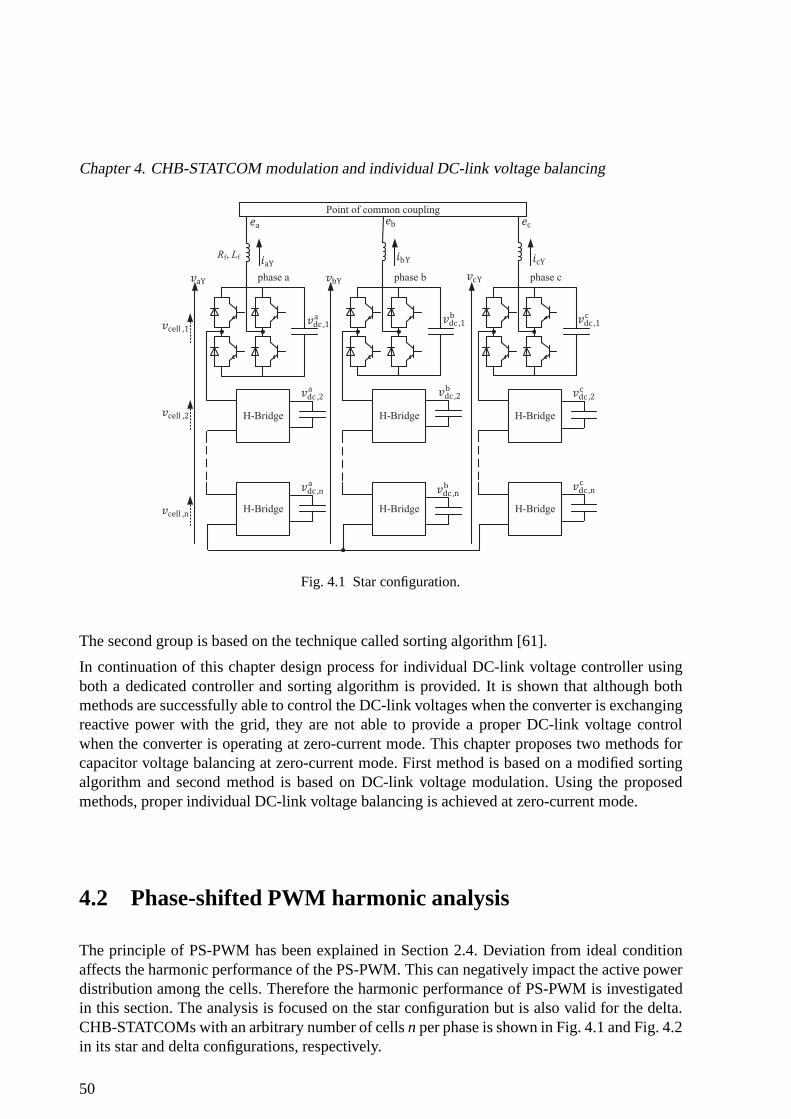
Chapter 4. CHB-STATCOM modulation and individual DC-link voltage balancing
phase bphase a phase c
H-Bridge
H-BridgeH-Bridge
H-BridgeH-Bridge
H-Bridge
Point of common coupling
Rf, Lf
Fig. 4.1 Star configuration.
The second group is based on the technique called sorting algorithm [61].
In continuation of this chapter design process for individual DC-link voltage controller usingboth a dedicated controller and sorting algorithm is provided. It is shown that although bothmethods are successfully able to control the DC-link voltages when the converter is exchangingreactive power with the grid, they are not able to provide a proper DC-link voltage controlwhen the converter is operating at zero-current mode. This chapter proposes two methods forcapacitor voltage balancing at zero-current mode. First method is based on a modified sortingalgorithm and second method is based on DC-link voltage modulation. Using the proposedmethods, proper individual DC-link voltage balancing is achieved at zero-current mode.
4.2 Phase-shifted PWM harmonic analysis
The principle of PS-PWM has been explained in Section 2.4. Deviation from ideal conditionaffects the harmonic performance of the PS-PWM. This can negatively impact the active powerdistribution among the cells. Therefore the harmonic performance of PS-PWM is investigatedin this section. The analysis is focused on the star configuration but is also valid for the delta.CHB-STATCOMs with an arbitrary number of cellsn per phase is shown in Fig. 4.1 and Fig. 4.2in its star and delta configurations, respectively.
50

4.2. Phase-shifted PWM harmonic analysis
H-Bridge
H-Bridge
phase a phase cphase b
H-BridgeH-Bridge
H-BridgeH-Bridge
Point of common coupling
Rf, Lf
Fig. 4.2 Delta configuration.
The PS-PWM harmonic analysis here is focused on phasea of the star configuration (Fig. 3.1).Analogous considerations can be drawn for the other two phases. The switching pattern for thevalves in the cells of the converter is here obtained using unipolar switching. As mentionedearlier, the basic principle of PS-PWM is to phase-shift thecarriers for each cell in the samephase leg in order to cancel a specific set of harmonics in the total output voltage. Optimumharmonic cancellation is achieved by phase-shifting each cell carrier by(k−1)π/
N, whereNis the total number of cells in each phase andk refers to the cell number. Denoting withfcr
the carrier frequency, the selected phase-shift between the carriers allows cancellation of theharmonic components up to 2fcrN in the total output phase voltage. Using asymmetrical regularsampled reference and double-edge carrier, the harmonic components of each cell in phaseacan be found as [62]
Vcell,k =4Vdc
π
∞
∑h=1
Mf
hJh(
hπMa
2Mf)sin(h
π2)cos(hω0t)+
+4Vdc
π
∞
∑h=1
∞
∑l=−∞
1q
J(2l−1)(qπ2
Ma)cos[(h+ l−1)π]×
×cos[2hωcr+(2l−1)ω0]t +2h(k−1)π
N+(2l−1)θ0
(4.1)
51
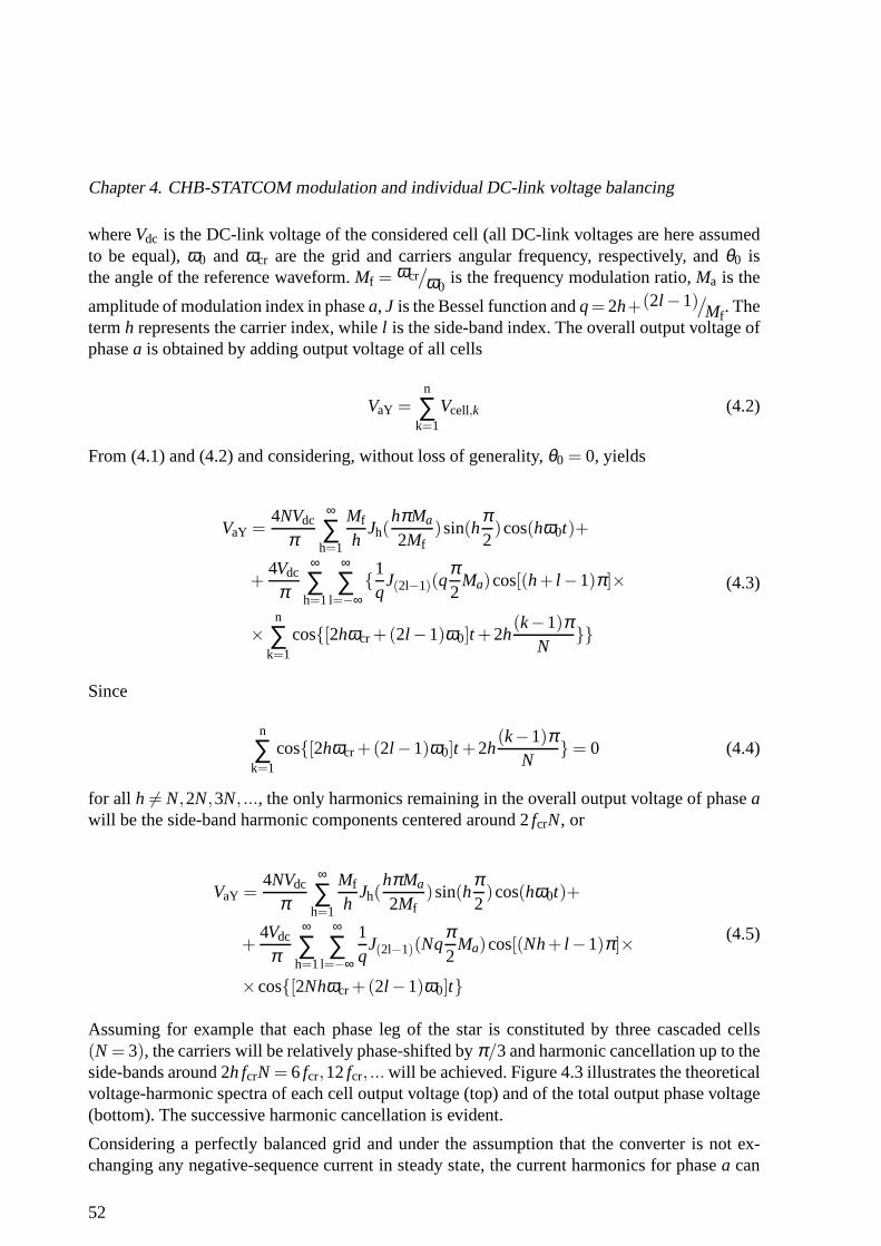
Chapter 4. CHB-STATCOM modulation and individual DC-link voltage balancing
whereVdc is the DC-link voltage of the considered cell (all DC-link voltages are here assumedto be equal),ω0 and ωcr are the grid and carriers angular frequency, respectively,and θ0 isthe angle of the reference waveform.Mf = ωcr
/
ω0is the frequency modulation ratio,Ma is the
amplitude of modulation index in phasea, J is the Bessel function andq=2h+(2l−1)/Mf
. Thetermh represents the carrier index, whilel is the side-band index. The overall output voltage ofphasea is obtained by adding output voltage of all cells
VaY =n
∑k=1
Vcell,k (4.2)
From (4.1) and (4.2) and considering, without loss of generality, θ0 = 0, yields
VaY =4NVdc
π
∞
∑h=1
Mf
hJh(
hπMa
2Mf)sin(h
π2)cos(hω0t)+
+4Vdc
π
∞
∑h=1
∞
∑l=−∞
1q
J(2l−1)(qπ2
Ma)cos[(h+ l−1)π]×
×n
∑k=1
cos[2hωcr+(2l−1)ω0]t +2h(k−1)π
N
(4.3)
Since
n
∑k=1
cos[2hωcr+(2l −1)ω0]t +2h(k−1)π
N= 0 (4.4)
for all h 6= N,2N,3N, ..., the only harmonics remaining in the overall output voltageof phaseawill be the side-band harmonic components centered around 2fcrN, or
VaY =4NVdc
π
∞
∑h=1
Mf
hJh(
hπMa
2Mf)sin(h
π2)cos(hω0t)+
+4Vdc
π
∞
∑h=1
∞
∑l=−∞
1q
J(2l−1)(Nqπ2
Ma)cos[(Nh+ l−1)π ]×
×cos[2Nhωcr+(2l−1)ω0]t
(4.5)
Assuming for example that each phase leg of the star is constituted by three cascaded cells(N = 3), the carriers will be relatively phase-shifted byπ/3 and harmonic cancellation up to theside-bands around 2h fcrN = 6 fcr,12fcr, ... will be achieved. Figure 4.3 illustrates the theoreticalvoltage-harmonic spectra of each cell output voltage (top)and of the total output phase voltage(bottom). The successive harmonic cancellation is evident.
Considering a perfectly balanced grid and under the assumption that the converter is not ex-changing any negative-sequence current in steady state, the current harmonics for phasea can
52

4.2. Phase-shifted PWM harmonic analysis
Fig. 4.3 Theoretical harmonic spectra; Top: cell output voltage; bottom: total phase lega voltage.N = 3,Ma = 0.9, Mf = 20,Vdc = 0.3 pu
be calculated as1
IaY =VaY−Ea
Z(4.6)
with Z the impedance of the filtering stage between the grid and the converter (calculated at thefrequency of interest) andEa the grid-voltage phasor for phasea. Observe that (4.6) considersthe phase-to-neutral voltageVaY for the computation of the line current and is therefore valid forsingle-phase systems only. In a three-phase CHB-STATCOM, the harmonic spectra in the cur-rent is determined by the phase-to-phase voltage; in the phase-to-phase voltage of the converter,some harmonics will be canceled [62] and therefore will not appear in the current waveform.However, this harmonic cancellation will not affect the analysis carried out in this thesis.
According with (4.6), the line current and phase voltage will present the same harmonic spectra,with the harmonic attenuation and phase change provided by the filter impedance. Observe thatsimilar investigation can be performed for the delta configuration, where the grid phase voltageEa in (4.6) must be replaced with the grid line-to-line voltageandVaY must be replaced byVa∆in order to obtain the branch currentIa∆ (see Fig. 4.2).
4.2.1 Effect of side-band harmonics on the active power
The harmonic components in (4.1) can be divided into two maingroups: fundamental compo-nent and side-band harmonics around it (first term in (4.1)),and carrier harmonics and theircorresponding side-band harmonics (second term in (4.1)).In order to simplify the descrip-
1If the converter exchanges both positive- and negative-sequence current with the grid, the common-modevoltage of the converter must be controlled to a non-zero value to guarantee DC-voltage balancing. In this case,following the same approach described in this section, the contribution of positive- and negative-sequence compo-nents to the active power distribution between the cells canbe evaluated using Fortescue Theory and superpositioneffect. Similar consideration holds for the delta configuration of the CHB-STATCOM.
53

Chapter 4. CHB-STATCOM modulation and individual DC-link voltage balancing
tion, both the fundamental component and side-band harmonics around it are here denoted asbase-band harmonics.
According to (4.1) and consideringN = 3, the phase angle of the carrier side-band harmonicsaround 2h fcr for each cell is equal to2h(k−1)π/
3. These phase angles at 6fcr (h = 3) areequal to 0,2π ,4π for each cell. Therefore, the harmonic components at 6fcr are in phase witheach other. Their amplitudes are also equal. On the other hand, the harmonic phase angles at2 fcr (h = 1) are equal to 0,2π/
3,4π/
3 and at 4fcr (h = 2) are equal to 0,4π/3,
2π/3 for each
cell. This means that the side-band harmonics for each cell around 2fcr and 4fcr have differentphase angle.
Interaction between current and voltages harmonics with the same frequency can lead to activepower, depending on their relative phase displacement. If this interaction occurs at carrier side-band harmonics around 2fcr (h = 1) or 4fcr (h = 2), the result will be a different active powerflowing in the DC-link capacitor of the different cells, due to the difference in carrier phaseangle described above. Both base-band and carrier harmonics of the current can interact withcell voltage harmonics. However, the interaction between cells voltage carrier harmonics andcurrent base-band harmonics can only occur when low switching frequency for the cell is used,due to the essence of the Bessel function as it will be shown later in this section.
To investigate this interaction and its impact on active power distribution among cells, two casestudies are here considered: low switching frequency for the cell (500 Hz and below, typicalin systems with a high number of cells per phase leg) and high switching frequency (above500 Hz, typical in systems with reduced number of cascaded cells per phase leg). Note thatthis distinction between low and high switching frequency is here intended as the possibility ornot of interaction between voltage side-band harmonics andcurrent base-band harmonics; thisis dictated by the shape of the Bessel function in (4.1): practically, the Bessel function can beconsidered zero when|l|> 10, meaning that for frequencies above 500 Hz interaction betweenthese group of harmonics can be neglected. Figure 4.4 shows aschematic representation ofthe different harmonic components and their location for both low (top) and high switchingfrequencies (bottom).
Case study #1, Low switching frequency
Considering 50 Hz grid frequency and, for example, 100 Hz switching frequency, it can berealized from the top plot in Fig. 4.4 that the voltage cell side-band harmonics correspond toh = 1 andh = 2; the base-band harmonics for the current are located at thesame harmonicorders. This would indicate that for low switching frequency there are interactions between thecell voltage side-band harmonics and the base-band currentharmonics. Since the phase angleof the cell voltage side-band harmonics corresponding toh = 1 andh = 2 are not equal, theirinteraction with the current base-band harmonics lead to different active power at each cell.
54

4.2. Phase-shifted PWM harmonic analysis
Fig. 4.4 Voltage and current harmonic spectra; Top: low switching frequency; bottom: high switchingfrequency.
Case study #2, High switching frequency
According to the bottom figure, for high switching frequency(here considered 1 kHz), no inte-raction occurs between the voltage cells side-band harmonics and the base-band current harmo-nics. This is because the interaction occurs in the side-band harmonics correspond toh = 1 andl =−19, andh = 2 andl = −39, where (as mentioned earlier) the Bessel function in (4.1) canbe considered zero. This would indicate that for high switching frequency there is no interactionbetween voltage and current harmonics, thus the active power should be uniformly distributedbetween the different cells. However, interaction might still occur at carrier harmonics level.
To understand this, the star configuration is simulated in PSCAD with the system parametersreported in Table 3.1. Ideal DC sources are used instead of actual capacitors in the cells and acarrier frequency of 1 kHz for the high switching case and 100Hz for the low switching caseare considered. An illustrative example of the uneven active power distribution among the cellsof the same phase leg is given in Fig. 4.5 for both low and high switching frequency case.
55

Chapter 4. CHB-STATCOM modulation and individual DC-link voltage balancing
Fig. 4.5 Active power of each cells output after low pass filtering with cut off frequency of 20 Hz; Left:Mf = 2; right: Mf = 20.
Observe that the number of cells is kept equal for the two cases. When the switching frequency islow, there is always an interaction between cell voltage carrier harmonics and current base-bandharmonics. If the switching frequency is high, the interaction is between the carrier harmonicsonly. As a result, the active power in the three cells is not equal. Observe that the total activepower of one phase is not zero due to the losses in filter reactor and semiconductors elements.
In case of high switching frequency, the interaction occursbetween voltage and current side-band harmonics. It has been shown that current carrier harmonics corresponding toh = 1 andh = 2 are canceled due to the phase-shift between carriers. However, the theoretical analysispresented earlier in this section is based on the assumptionof a perfectly ideal converter. In suchcondition, the converter can be considered as a linear amplifier where the DC-link voltages inthe different cells are equal, ideal carrier phase-shift isprovided for each cell and no delays. Anydeviation from ideal condition, such as diverge in DC-link voltages or non-ideal phase-shift inthe carriers, will lead to non-ideal cancellation of the harmonic components in the total outputvoltage and consequently in the current. This can be seen from the voltage/current harmonicspectra in Fig. 4.6.
Fig. 4.6 Current and voltage carrier side-band harmonics ath = 1 in case of high switching frequency(Mf = 20).
To quantify the effect of the harmonic interactions on the active power, the degree of unbalance
56

4.2. Phase-shifted PWM harmonic analysis
in the power is defined as
∆P =Pmax−Pmin
Pave(4.7)
with Pmax andPmin the maximum and minimum active power among the cells andPave the ave-rage power. The degree of unbalance in Fig. 4.5 withMf = 20 is 1.9, and withMf = 2 is 8.32.Observe that the degree of unbalance at high switching frequency is much lower than the oneat the low switching frequency, but still not zero. This indicates that in practical applications,where the DC sources are substituted with actual capacitors, in both cases the DC-link voltageof the cells will diverge. The DC-capacitor voltages will drift faster when low switching fre-quency is selected. This effect can be clearly seen in Fig. 4.7, where the same simulation hasbeen performed when the ideal DC sources have been replaced with actual capacitors. For thissimulation, the converter is exchanging 0.05 pu current with the grid and the needed controlloop to guarantee the convergence of the voltage across the individual cells (see Section 4.3)has been intentionally disabled. The left and the right figure shows the capacitor voltages whenusing fcr = 250 Hz and fcr = 1000 Hz, respectively. Observe that, for clarity of the figure,a post-processing low-pass filter has been utilized to remove the oscillations in the measuredcapacitor voltage and thereby highlight the voltage divergence.
Fig. 4.7 Simulation results of capacitor voltages in phasea of the star configuration. Left:fcr = 250 Hz;right: fcr = 1000 Hz.
4.2.2 Selection of frequency modulation ratio
In case of low switching frequency and according to (4.1), base-band harmonics are locatedat hω0 and carrier harmonics are located at 2hωcr+(2l −1)ω0. If the carrier frequencyωcr ischosen to be non-integer multiple of fundamental frequencyω0, the carrier harmonics will notbe located at base-band harmonics and consequently the interaction between these two sets ofharmonics will be removed. More details for this case can be found in [11]. Although the non-integer ratio effectively reduces the interaction betweenbase-band and carrier harmonics (mainproblem with low switching frequencies), it can also provide an improvement for the carrierharmonic interactions (main problem with high switching frequencies). However, the case ofhigh switching frequencies is more complicated and is investigated in the next section.
57

Chapter 4. CHB-STATCOM modulation and individual DC-link voltage balancing
4.2.3 Impact of non-integer frequency modulation ratio for high swit-ching frequencies
In case of high switching frequencies, the problem lies on the non-ideal cancellation of currentcarrier harmonics. As briefly mentioned earlier, the main reasons are: different modulation ratioamong cells, different capacitors size tolerance, different DC-link voltage among cells, errors incarriers phase-shift that lead to different pulse width among cells [63]. Any kind of mismatchbetween the modulation of the single cells (for example, sampling delay, blanking time etc.)can also be the reason of failure in ideal carrier harmonics cancellation.
In practice there will be some non-zero error associated with the phase angle of the carrierwaveforms. In order to show the impact of non-integerMf in dealing with this error, the ana-lysis here will be focused on one carrier harmonic componentand the number of cells will beconsidered to beN = 3. The analysis can be extended to any other harmonic component and forany number of cells.
Consideringh = 1, l = 1, θ0 = 0 and using (4.1) and (4.6), the output cell voltage and linecurrent for phasea are
Vcell,1 =4Vdc
π−Mf
2Mf +1J(1)(
2Mf +1Mf
π2
Ma)︸ ︷︷ ︸
V
×
×cos[(2ωcr+ω0)︸ ︷︷ ︸
ω
t +2θcr1] =V cos(ωt +2θcr1)
Vcell,2 =V cos(ωt +2θcr2)
Vcell,3 =V cos(ωt +2θcr3)
(4.8)
iaY =
3∑
i=1Vcell,i
Zω=
VZω
[cos(ωt +2θcr1−∠Zω)+
+cos(ωt +2θcr2−∠Zω)+
+cos(ωt +2θcr3−∠Zω)]
(4.9)
whereθcr1,θcr2,θcr3 are the initial phase angles of the carriers for each cell and∠Zω is the filterimpedance angle, here considered equal toπ/
2 (pure inductive filter).
Before proceeding in the calculation of the active power foreach cell, the initial phase angle ofthe carriersθcr1, θcr2, θcr3 should be determined. Figure 4.8 shows as an example a comparisonbetween a carrier with integer carrier frequency ratio ofMf = 2 ( fcr = 100 Hz with solid line)and non-integer carrier frequency ratio ofMf = 1.8 ( fcr = 90 Hz with dashed line). Observethat for this figureMf is set small for clarity of the illustration. It can be seen from the figurethat unlike the integer case, the initial phase of the carrier at the beginning of each fundamentalperiod (t = 0.02 s,t = 0.04 s, ...) is not fixed when non-integer frequency modulationratio isapplied.
58

4.2. Phase-shifted PWM harmonic analysis
0 0.01 0.02 0.03 0.04 0.05 0.060
0.2
0.4
0.6
0.8
1
modulation indexintegernon−integer
Fig. 4.8 Comparison between modulation index and carrier with integer (fcr = 100Hz) and non-integer( fcr = 90Hz) ratio.
Assume that the carrier initial phase angle in the first fundamental cycle is equal to zero andlet us denote withfcri the carrier frequency in case of an integerMf, while f0 is the systemfundamental frequency. For a non-integerMf, the corresponding carrier frequency,fcrn, can berepresented as
fcrn = fcri ±θ f02π
(4.10)
with θ the relative phase-shift between two carriers after one fundamental cycle. Alternatively,after half of a fundamental cycle we get
fcrn = fcri ±θ f0π
(4.11)
Therefore, for analysis purpose the carrier frequency for the non-integer case can be representedas the sum of the frequencyfcri and an additional term that takes into account the relative phase-shift between the two carriers. Considering, as an example,1 kHz and 100 Hz as high and lowswitching frequencies, the corresponding non-integer frequency that providesπ
/
3 initial phaseangle after one fundamental period for this example can be 1008.3 Hz or 991.7 Hz for the highand 108.3 Hz or 91.7 Hz for the low switching frequency.
Using (4.11), the initial carrier phase angles after each half of a fundamental period is
θcr1 =π( fcrn− fcri)
f0(hf −1)
︸ ︷︷ ︸
θ1
+εn(θ1)
θcr2 =π3+
π( fcrn− fcri)
f0(hf −1)
︸ ︷︷ ︸
θ2
+εn(θ2)
θcr3 =2π3
+π( fcrn− fcri)
f0(hf −1)
︸ ︷︷ ︸
θ3
+εn(θ3)
(4.12)
59

Chapter 4. CHB-STATCOM modulation and individual DC-link voltage balancing
wherehf refers to the half period number. For example, to find the phase angle of each carrierafter three half period,hf should be set to 3. The termεn in (4.12) is introduced to model anyphase-shift error between the carriers, which is unavoidable in practical implementations. Thiserror function is difficult to quantify but a function that provides a unique error for each initialphase angle can be considered as
εn(θ) = knθ (4.13)
with kn a constant coefficient. It should be noted that the selectionof this error function doesnot affect the final result.
The active power for each cell calculated over a given numberof half-cycles (hf = hfd) for agiven non-integer carrier frequency can be obtained by multiplying the current and voltage in(4.8) and extracting the constant terms, as
Pcell,1 =V 2
2Zω hfd
hfd
∑hf=1
[−sin(2θcr1−2θcr2)−sin(2θcr1−2θcr3)]
Pcell,2 =V 2
2Zω hfd
hfd
∑hf=1
[−sin(2θcr2−2θcr3)−sin(2θcr2−2θcr1))
Pcell,3 =V 2
2Zω hfd
hfd
∑hf=1
[−sin(2θcr3−2θcr2)−sin(2θcr3−2θcr1))
(4.14)
and in general, forN number of cells is
Pcell,k =V 2
2Zωhfd
hfd
∑hf=1
N∑
nn=1nn 6=k
−sin(2θcrk−2θcrnn)
θcri =π(i−1)
N+
2π( fcrn− fcri)
2 f0(hf −1)
︸ ︷︷ ︸
θi
+εn(θi)(4.15)
The final goal is to find a value forfcrn− fcri that provides an equal active power in all cellsin the minimum time, i.e. in the minimum possible number ofhfd, in order to minimize thedeviation in the capacitor voltages.
According to (4.14) the term V 2
2Zω hfdis the same for each cell and thus it can be ignored in the
calculation of the power since it has the same effect on each cell. ConsideringN = 3, kn = 0.01,f0 = 50 Hz, Fig. 4.9 shows the active power of each cell as a function of the termfcrn− fcri. Thetop plot shows the active power over one half period, second plot shows the active power overtwo half periods, third plot shows the active power over three half periods. As it can be observed,only when selectinghfd = 3 equal active power can be achieved (withfcrn− fcri = 16.67 Hz).Close up picture of this case is shown in the bottom plot.
The same process is implemented for different number of cells (i.e.N = 4,5, ...) and the resultsare shown in Fig. 4.10. The top plot shows the minimum number of half periods needed toachieve equal active power among cells, while bottom plot shows the correspondingfcrn− fcrivalue (lowest value).
By curve fitting the obtained results, the optimum solution for fcrn− fcri that provides equalactive power among cells in the minimum number of half cycle period is
60

4.2. Phase-shifted PWM harmonic analysis
0 5 10 15 20 25 30 35 40 45 50−0.1
0
0.1
Pow
er [W
]
one half period
P
cell 1
Pcell
2
Pcell
3
0 5 10 15 20 25 30 35 40 45 50−0.1
0
0.1
Pow
er [W
]
two half periods
P
cell 1
Pcell
2
Pcell
3
0 5 10 15 20 25 30 35 40 45 50−0.1
0
0.1
Pow
er [W
]
three half periods
P
cell 1
Pcell
2
Pcell
3
16.6 16.61 16.62 16.63 16.64 16.65 16.66 16.67 16.68 16.69 16.7−0.05
0
0.05
Pow
er [W
]
fcrn
−fcri
[Hz]
Fig. 4.9 Active power of each cell forN = 3; First on top: after one half period; second: after two halfperiods; third: after three half periods; forth: close up picture for three half periods.
2 3 4 5 6 7 8 9 102
4
6
8
10
X: 3Y: 3
min
um n
umbe
r of
half
perio
ds X: 6Y: 6
X: 8Y: 8
2 3 4 5 6 7 8 9 105
10
15
20
25
X: 3Y: 16.67
f crn−
f cri
number of cells n
X: 6Y: 8.333 X: 8
Y: 6.25
Fig. 4.10 Active power and minimum number of half period for different number of cells; top: minimumnumber of half period; bottom:fcrn− fcri value.
61

Chapter 4. CHB-STATCOM modulation and individual DC-link voltage balancing
fcrn− fcri =± f0N
(4.16)
For example, choosing the integer carrier frequency of 1 kHzand for a fundamental frequencyof 50 Hz, the corresponding non-integer frequency forN = 3 is 1016.66 Hz or 983.33 Hz.Following the same procedure, the optimum solution forfcrn− fcri that provides equal activepower among cells but in minimum number of full fundamental cycles (instead of half cycles)is
fcrn− fcri =± f02N
(4.17)
Similar to the previous example, choosing the integer carrier frequency of 1 kHz, the corres-ponding non-integer frequency forN = 3 is 1008.33 Hz or 991.66 Hz. Both of these frequenciesprovide the same results. In the following simulation results the higher switching frequency ischosen.
4.2.4 Simulation results
The star configuration with system parameters in Table 3.1 and using DC sources instead ofactual capacitors is simulated in PSCAD with integer and non-integer frequency modulationratio for both low and high switching frequencies. Figure 4.11 shows the output active power ofeach cell in phasea for different carrier frequencies. Low-pass filtering withcut off frequencyof 20 Hz is applied to enhance the difference in the cells active power.
As discussed earlier, using integer carrier frequencies of100 Hz and 1 kHz leads to diffe-rent active power among the cells. As described in Section 4.2.3, optimum non-integer car-rier frequencies that provides equal active power in minimum number of half-fundamental cy-cle are 116.66 Hz and 1016.66 Hz; similarly, optimum non-integer carrier frequencieswhichprovides equal active power in minimum number of full-fundamental cycle are 108.33 Hzand 1008.33 Hz. It can be seen that although both 116.66 Hz, 1016.66 Hz and 108.33 Hz,1008.33 Hz provide equal active power among cells, the selection of 116.66 Hz or 1016.66 Hzleads to less deviation in the cell active powers. Carrier frequencies of 125 Hz and 1025 Hz areexamples of non-optimal non-integer carrier frequency. Itcan be seen from Fig. 4.11 (bottom)that, regardless the use of a non-integerM f , the active powers are not equal in this case.
In order to show the effect of the frequency modulation ratioon voltage balancing of the capaci-tors, the ideal DC sources in the cells are replaced with actual capacitors. For these simulations,the star configuration is controlled to inject 0.052 pu reactive power into the grid. Figure 4.12shows the capacitors voltages in phasea when using carrier frequencies offcr = 1000 Hz,1008.3 Hz, 1016.6 Hz and 1025 Hz. Observe that while withfcr = 1000 Hz the capacitorvoltages will deviate from the desired value, the use of a non-integer carrier frequency offcr = 1016.6 Hz or fcr = 1008.3 Hz will assist in keeping the voltages close to the refe-rence. It can also be observed that the capacitor voltages are still slowly diverging when usingfcr = 1025 Hz, due to the non-optimal selection of this ratio. Similar results can be obtainedwhen using low switching frequency for the converter cells,as shown in Fig. 4.13, wherefcr = 250 Hz is used for the integer case and around it for the non-integer cases. Again, a
62

4.2. Phase-shifted PWM harmonic analysis
Fig. 4.11 Active power of each cell in phasea after low pass filtering for different carrier frequencies.
more uniform distribution of the active power in the different cells is obtained when selectingthe carrier frequency according with (4.16) or (4.17).
The analysis carried out until now only focuses on the error in the phase shift between thedifferent carriers and the presented results consider onlythis as a deviation from the ideal con-ditions. However, as mentioned earlier, in practical applications any kind of mismatch betweenideal and actual conditions will have an impact on the distribution of the active power betweenthe converter cells. As an example, Fig. 4.14 shows the capacitor voltages in phasea withfcr = 1000 Hz, 1008.3 Hz, 1016.6 Hz and 1025 Hz when a tolerance of 10% is considered forthe DC-capacitor sizes in the simulation model. It can be observed that although non-integerM f
helps in keeping the voltages close to the reference, still for the simulated case it is not possibleto provide a perfectly even active power distribution amongthe cells. As it can be understoodfrom the analysis carried out in the previous sections, the impact of this kind of deviationswill be more significant when lowering the switching frequency. Therefore, it is of importanceto stress that an individual balancing controller must be implemented in actual installations, re-gardless the selection ofMf. Individual balancing control can be implemented by eithera closedloop controller or by the sorting algorithm. Both of these methods and their implementation areprovided in the next chapters.
63

Chapter 4. CHB-STATCOM modulation and individual DC-link voltage balancing
Fig. 4.12 Capacitors voltages in phasea with fcr = 1000 Hz, 1008.3 Hz, 1016.6 Hz and 1025 Hz.
Fig. 4.13 Capacitors voltages in phasea with fcr = 250 Hz, 258.3 Hz, 266.6 Hz and 275 Hz.
64

4.3. Individual DC-link voltage controller
Fig. 4.14 Capacitors voltages in phasea with fcr = 1000 Hz, 1008.3 Hz, 1016.6 Hz and 1025 Hz andwith tolerance of±10% in DC capacitor sizes.
4.3 Individual DC-link voltage controller
The control system described in Chapter 3 provides identical modulation index for each cell.The basic idea of the individual DC-link voltage controlleris to include an extra control loop inorder to modify the modulation index for each cell and thus provide the required active powerfor individual DC-link voltage balancing.
Each modulation index is characterized by an amplitude and aphase angle. The method pro-posed in [64–66] modifies the amplitude and phase angle of each modulation index individuallyto provide the required active power for each cell. Modifying the modulation index by voltagevector superposition method is proposed in [8,67–69].
Among the proposed methods, active voltage vector superposition method is more robust [69].Therefore, the method used in [8] is used here for the individual DC-link voltage controller.
For STATCOM applications, the reactive component of the current is typically much larger thanthe active component (iq >> id). Due to this fact and also considering to have a fast and precisecurrent controller (iqref ≈ iq) it is possible to estimate the current in each phase of the star as
iaY =√
2√3iqrefsin(θ)
ibY =√
2√3iqrefsin(θ − 2π
3 )
icY =√
2√3iqrefsin(θ + 2π
3 )
(4.18)
where√
2√3
is the coefficient used for power invariant transformation from dq-reference frameto three-phase system and “ ˆ ” is to indicate the estimated quantities. Since the current is
65

Chapter 4. CHB-STATCOM modulation and individual DC-link voltage balancing
Fig. 4.15 Closed loop block diagram of the individual DC-link voltage controller.
leading/lagging by 900 with voltage, the current amplitudes are multiplied by sin(θ).The voltage components that are superposed to the referencevoltage of each cell at each phaseare
va,ki,Y = kind,Y(va2
dc,k− v2cla)sin(θ)
vb,ki,Y = kind,Y(vb2
dc,k− v2clb)sin(θ − 2π
3 )
vc,ki,Y = kind,Y(vc2
dc,k− v2clc)sin(θ + 2π
3 )
(4.19)
wherekind,Y is a proportional gain,vcla,vclb,vclc are the cluster voltages (average of DC-linkvoltage in each phase) in phasea,b,c andva
dc,k,vbdc,k,v
cdc,k are the DC-link voltage ofkth cell
in phasea,b,c. The voltage components that are superposed to the reference voltage of eachcell are AC signals in phase with the currents, which thus form an active power component tobalance the DC-link voltages.
It should be mentioned that the difference between the cluster control loop explained in Chap-ter 3 and the individual DC-link voltage controller is that the cluster control loop takes care ofthe cluster voltage and controls it to the reference voltagewhile the individual DC-link voltagecontroller takes care of the DC-link voltage in each cell. The purpose of the individual DC-linkvoltage controller is to not allow the DC-link voltage to diverge from the cluster voltage.
The active power for the DC-link voltage balancing of thekth cell in phasea can be written as
12
Cs(va2
dc,k) =
∣∣∣va,k
i,Y
∣∣∣
∣∣iaY
∣∣
2(4.20)
Replacing the variable∣∣∣va,k
i,Y
∣∣∣ and
∣∣iaY
∣∣ from (4.18) and (4.19) into (4.20), the closed loop block
diagram of the individual DC-link voltage controller can beshown as Fig. 4.15. The closed-looptransfer function fromv2
cla to va2
dc,k is given by
Gind,Y =va2
dc,k
v2cla
=
kind,Y iqref√
2
C√
3
s+kind,Y iqref
√2
C√
3
=αind
s+αind(4.21)
66

4.3. Individual DC-link voltage controller
whereαind is the closed-loop bandwidth of the individual DC-link voltage controller. From(4.21), the proportional gain of the individual DC-link voltage controller is given by
kind,Y =
√3Cαind√2iqref
(4.22)
It can be observed from (4.22) that the individual balancingcontrol does not work wheniqrefis zero. Therefore this method is unable to provide the individual DC-link voltage control atzero-current mode. This problem and its solutions will be discussed in the next part of thischapter.
Following the same design process for the delta configuration, three phase estimated branchcurrents of the delta are
ia∆ =√
23 iqrefsin(θ + π
6)
ib∆ =√
23 iqrefsin(θ + π
6 − 2π3 )
ic∆ =√
23 iqrefsin(θ + π
6 +2π3 )
(4.23)
where π6 is the phase shift between the line and the branch currents. The voltage components
which are superposed to the reference voltage of each cell ateach phase are
va,ki,∆ = kind,∆(va2
dc,k− v2cla)sin(θ + π
6)
vb,ki,∆ = kind,∆(vb2
dc,k− v2clb)sin(θ + π
6 − 2π3 )
vc,ki,∆ = kind,∆(vc2
dc,k− v2clc)sin(θ + π
6 +2π3 )
(4.24)
The proportional gain is then given by
kind,∆ =3Cαind√
2iqref(4.25)
Figure. 4.16 shows the overall control block diagram of CHB-STATCOMs including individualDC-link voltage controller.
4.3.1 Simulation results
The CHB-STATCOMs with system parameters of Table 3.1 are simulated in PSCAD includingthe individual DC-link voltage controller. In order to avoid the interaction between the clusterand individual DC-link voltage controller, the individualcontroller is intentionally designed tobe slower than the cluster control loop. The closed loop bandwidth of the individual DC-link
67

Chapter 4. CHB-STATCOM modulation and individual DC-link voltage balancing
DC-link
voltage control
current
control
PS
-PW
M
Filter
Filter
Individual
DC-link
voltage
control
...
...
...
...
...
...
++
++
++
gate
signals
Filter...
... +-
square sin( ) ...
Filter...
... +-
square sin( - )...
Filter...
... +-
square sin( + ) ...
Individual DC-link voltage control
(a)
(b)
q-controller
e-controller
(
(
(
(
Fig. 4.16 Overall control block diagram CHB-STATCOMs with individual DC-link voltage controller;(a): Overall control; (b): individual DC-link voltage controller.
68
4.4. Individual DC-link voltage control using sorting algorithm
2.7 2.8 2.9 3 3.1 3.2 3.3 3.4
0.29
0.3
0.31
0.32
Vol
tage
[pu]
starfcr
=1000 Hz
2.7 2.8 2.9 3 3.1 3.2 3.3 3.4−0.01
0
0.01
Vol
tage
[pu]
Time [S]
2.7 2.8 2.9 3 3.1 3.2 3.3 3.40.52
0.525
0.53
Vol
tage
[pu]
deltafcr
=1000 Hz
2.7 2.8 2.9 3 3.1 3.2 3.3 3.4−0.01
0
0.01
Vol
tage
[pu]
Time [S]
Fig. 4.17 DC-link voltage results of CHB-STATCOMs; top: filtered DC-link voltages; bottom: outputsof the individual DC-link voltage controller. (with carrier frequency of 1 kHz)
voltage controller is set to 1 Hz, i.e. 5 time below the bandwidth of the cluster control loopbandwidth.
Figure 4.17 shows the filtered DC-link voltages and the output of the individual DC-link voltagecontroller of each cell in phasea for both star and delta when integer carrier frequency of 1 kHzis used. The reference reactive current is set to 0.3 pu. The individual DC-link voltage controlleris not activated in the beginning of the simulation and activated att = 3 S. Figure 4.17 (top)shows the ability of the individual DC-link voltage controller to control the DC-link voltages.
Figure 4.18 shows the obtained simulation results when non-integer carrier frequency of 1016.67Hz is used instead. It can be observed from Fig. 4.18 that by using non-integer frequency modu-lation ratio, the individual DC-link voltage controller puts much less effort in controlling theDC-link voltages. This shows the advantage of using non-integer frequency modulation ratioinstead of the integer one.
4.4 Individual DC-link voltage control using sorting algorithm
Individual DC-link voltage control presented in the previous section is based on the superposi-tion of a voltage component to the reference voltage. This modification of the reference voltagefor each cell can degrade the harmonic performance of the PS-PWM [60]. This is due to thefact that the perfect harmonic cancellation will be achieved when all the modulation indexes areidentical. Another problem caused by the individual DC-link voltage control using the controlloop method is the interaction between the individual DC-link voltage controller and the clustercontrol loop. Due to these problems, another technique for controlling the DC-link voltages hasbeen introduced, based on the sorting algorithm. The sorting algorithm allows the modulationscheme to inherently balance the DC-link voltages, thus removing the need for any control loop.
In sorting algorithm when the converter absorbs active power (charging mode) the cells with the
69
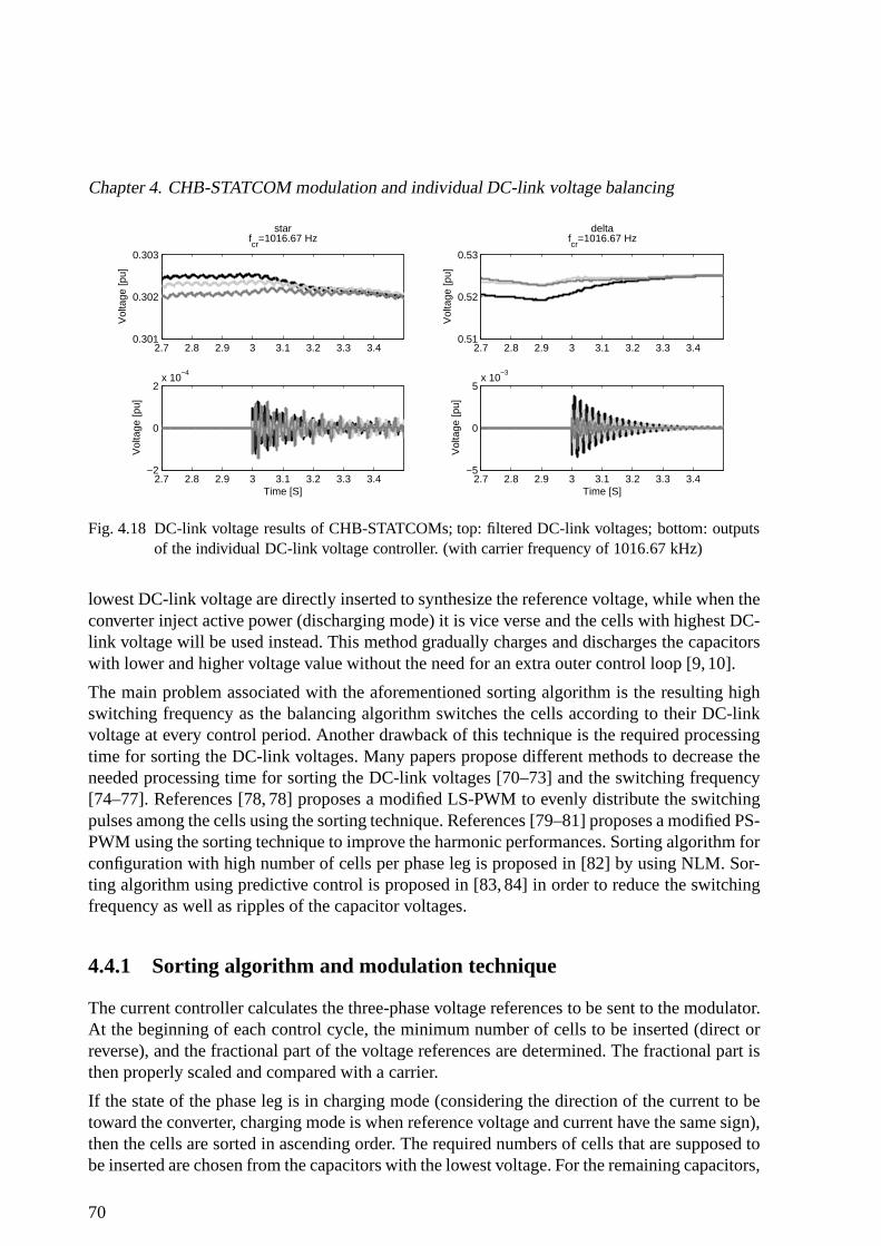
Chapter 4. CHB-STATCOM modulation and individual DC-link voltage balancing
2.7 2.8 2.9 3 3.1 3.2 3.3 3.40.301
0.302
0.303
Vol
tage
[pu]
starfcr
=1016.67 Hz
2.7 2.8 2.9 3 3.1 3.2 3.3 3.4−2
0
2x 10
−4
Vol
tage
[pu]
Time [S]
2.7 2.8 2.9 3 3.1 3.2 3.3 3.40.51
0.52
0.53
Vol
tage
[pu]
deltafcr
=1016.67 Hz
2.7 2.8 2.9 3 3.1 3.2 3.3 3.4−5
0
5x 10
−3
Vol
tage
[pu]
Time [S]
Fig. 4.18 DC-link voltage results of CHB-STATCOMs; top: filtered DC-link voltages; bottom: outputsof the individual DC-link voltage controller. (with carrier frequency of 1016.67 kHz)
lowest DC-link voltage are directly inserted to synthesizethe reference voltage, while when theconverter inject active power (discharging mode) it is viceverse and the cells with highest DC-link voltage will be used instead. This method gradually charges and discharges the capacitorswith lower and higher voltage value without the need for an extra outer control loop [9,10].
The main problem associated with the aforementioned sorting algorithm is the resulting highswitching frequency as the balancing algorithm switches the cells according to their DC-linkvoltage at every control period. Another drawback of this technique is the required processingtime for sorting the DC-link voltages. Many papers propose different methods to decrease theneeded processing time for sorting the DC-link voltages [70–73] and the switching frequency[74–77]. References [78, 78] proposes a modified LS-PWM to evenly distribute the switchingpulses among the cells using the sorting technique. References [79–81] proposes a modified PS-PWM using the sorting technique to improve the harmonic performances. Sorting algorithm forconfiguration with high number of cells per phase leg is proposed in [82] by using NLM. Sor-ting algorithm using predictive control is proposed in [83,84] in order to reduce the switchingfrequency as well as ripples of the capacitor voltages.
4.4.1 Sorting algorithm and modulation technique
The current controller calculates the three-phase voltagereferences to be sent to the modulator.At the beginning of each control cycle, the minimum number ofcells to be inserted (direct orreverse), and the fractional part of the voltage referencesare determined. The fractional part isthen properly scaled and compared with a carrier.
If the state of the phase leg is in charging mode (consideringthe direction of the current to betoward the converter, charging mode is when reference voltage and current have the same sign),then the cells are sorted in ascending order. The required numbers of cells that are supposed tobe inserted are chosen from the capacitors with the lowest voltage. For the remaining capacitors,
70

4.4. Individual DC-link voltage control using sorting algorithm
the one with the lowest voltage is chosen to be modulated by the fractional part of the voltagereference. The rest of the cells are fully bypassed.
The same process can be used for discharging mode (voltage and current at each phase are inopposite sign), where the cells are sorted in descending order.
For practical implementation,f loor and rem commands can be used for the sorting PWM.f loor(x) returns the nearest positive integer lower or equal tox. rem(a
/
b) returns the fractionalpart ofa dividedb. For example, if the reference voltage in one phase is -19kV and each cellvoltage isVdc = 3.33 kV , then f loor(−19/
3.33)=5 andrem(−19/3.33)=-2.35. The fractional
part of the reference voltage is normalized with the cell voltage and will be used to modulate acell. In this example eventually 5 cells must be reversed inserted and one cell must be modulatedwith the fractional part.
4.4.2 Zero-current operating mode
Although sorting algorithm is an effective solution for voltage balancing when the converter isexchanging current with the grid, less attention has been paid for zero-current operating mode(STATCOM in standby mode) in the literature. Sorting algorithm needs current sign informationto provide a correct sorting pattern. As a consequence, whenthe exchanging current that flows inthe cells is zero, the sorting algorithm is unable to take thecorrect insertion decision for properbalancing of the DC-link voltages. In practical applications, this is even more problematic whennoise is also added in the measured current signal. The problem of system operation at zero-current mode also exists when using individual DC-link voltage control loop, as described inSection 4.3.
Here, two methods for capacitor voltage balancing at zero-current mode are proposed. The firstmethod is based on a modified sorting algorithm, while the second method is based on DC-linkvoltage modulation. It is of importance to stress that the investigated methods are for zero-current mode only, since when a current circulates in the phase leg the classical or advancedsorting techniques can be adopted.
The proposed methods are meant for the star configuration. Although the same methods can beused for the delta configuration, it is of importance to consider that in this case, it is possibleto force a current that circulates inside the delta and thereby allow a uniform distribution ofthe active power among the different cells. This solution cannot be implemented in practicein the star case. For this reason, capacitor cells balancingis more challenging in star configu-ration, especially in case of zero (or more in general, very small) current exchange between thecompensator and the grid.
Figure 4.19 shows the principle of operation of unipolar PWMwhen the reference voltage ispositive. The reference value in Fig. 4.19 is the fractionalpart of the reference voltage.
As shown in the right figure, if the RMS value of the current becomes zero, the sign of the instan-taneous current will change in the middle of two sampling points. This implies a dischargingfollowing by a charging state during one control cycle. The same sign change is observablewhen reference voltage is negative: in this case, the instantaneous current is positive in the first
71

Chapter 4. CHB-STATCOM modulation and individual DC-link voltage balancing
Modulation index
Instantaneous current
Instantaneous current sign changes from negative to positive in the middle of two
sampling points
Sampling points
i
dcV
sT
t
t
Cell output voltagedcV
sT
s5.0 T
s5.0 T
Fig. 4.19 Zero-current mode operation in unipolar PWM and positive reference voltage; left: H-bridgeconverter; right: unipolar PWM principle.
half cycle and is negative in the second half. This implies again a discharging followed by acharging state during one control cycle.
The sorting algorithm determines the switching pattern during one control cycle based on thecharging or discharging mode; however the sign of the instantaneous current at zero-currentmode shows that a single detection in the beginning of each control cycle is not sufficient todetermine the sorting pattern. Therefore, the detection ofcharging or discharging, and conse-quently the sorting pattern, must be updated in the middle oftwo sampling points.
The conventional sorting algorithm is applied to a 19-levelstar configuration in PSCAD. Table4.1 shows the system parameters selected for the simulationstudy.
TABLE 4.1. SYSTEM AND CONTROL PARAMETERS
Parameters valuesRated powerSb 120 MVA , 1 puNominal line to line rms voltageVb 33 kV , 1 puFilter inductanceLf 4.33 mH , 0.15 puFilter resistorRf 0.136Ω , 0.015 puCapacitorsC 4 mF , 0.088 puDC-link voltage of each cellVdc 3.33 kV , 0.1 puNumber of cells per phaseN 9Carrier frequency for PWMfcr 500 HzGrid frequencyfo 50 HzCurrent control closed loop band widthαi 2π ×100 rad/secCluster control closed loop band widthαcl 2π ×5 rad/sec
In order to provide a more realistic model, the capacitors ineach cell are paralleled with aresistor. This resistor is to model the internal losses in the cell and is chosen to be different from
72

4.4. Individual DC-link voltage control using sorting algorithm
Fig. 4.20 DC-link voltages and line current in phasea without the proposed methods; top: line current;bottom: capacitor voltages.
cell to cell. In addition to the resistors, a±20% tolerance band is chosen for the capacitors sizes(3.2 to 4.8 mF). Note that the deviation here considered is large in order to stress the system andaccelerate the voltage deviation.
Figure 4.20 shows the simulation results when using the conventional sorting algorithm. Topplot shows the line current in phasea while the lower figure shows the DC-link voltages inphasea. Similar behavior can be observed for the other phases. All figures are showing themeasured quantities in pu. At t=0.9 s, the reactive current is changed from 0.35 pu to zero.Figure. 4.20 shows that conventional sorting algorithm is not able to provide proper individualcell balancing at zero-current mode.
Figure 4.21 shows a detail of a cell output voltage, line current between two sampling pointstogether with the interrupt signal. It can be observed from this figure that the sign of the currentis negative in the first half of the control period and changesto positive after almost half of theperiod, as anticipated earlier in this section. Theoretically, at zero-current operating mode, thecurrent sign changes exactly in the middle of the control period. This provides equal positive andnegative areas, leading to equal charging and discharging.Consequently, the DC-link voltageshould remain constant. However in practical applicationsthis symmetry will not be achieved,leading to slightly more charging or discharging area (as inthis specific example). Thereforethe DC-link voltages will not remain constant and diverge from their reference values.
4.4.3 Modified sorting algorithm
The first proposed method takes advantage of the knowledge ofthe sign of the current rippleas zero-current mode. In STATCOM applications even if the reactive current is zero, there isalways a small active current flowing in order to keep the charge of all capacitors and compen-sate for the losses. In this case the RMS value of the current is not zero. This is beneficial forthe sorting since a small flowing current with small ripple amplitudes can be used for the cells
73

Chapter 4. CHB-STATCOM modulation and individual DC-link voltage balancing
Fig. 4.21 Cell output voltage and line current together withmain interrupts.
sorting. However, measurement noise can affect the detection of charging or discharging mode.The noise amplitudes can become bigger than the actual current.
In this section a solution is proposed, which is independentfrom the current measurements.The proposed method assumes that the ripple current is bigger than the RMS value when theexchanging current is small and therefore the actual current can be approximated with its rippleonly.
As explained in the previous section, at zero-current mode the control cycles always start in adischarging mode and in the middle of the control cycle it should change to charging mode.Therefore, current and voltage measurements are not neededanymore to detect the charging ordischarging modes. In the proposed method, two sets of interrupts are used. The main interruptis synchronized with the top and bottom of the main carrier; this interrupt is used for samplingof the measured quantities. The second interrupt, located between the two sampling points isintroduced in order to indicate the point where the discharging mode should change to chargingmode. Whenever this interrupt is enabled, the sorting algorithm must change the sorting patternaccording to the new mode. It is of importance to stress that the modified sorting algorithmproposed here should be used for zero-current mode only. Thethreshold for the activation ofthe proposed controller is here set to 0.03 pu current.
The flowchart of the proposed algorithm is shown in Fig. 4.22.In the beginning of each maininterrupt, first the reference voltage is determined. Then,the number of cells that must be in-serted (direct or reverse) and fractional part of the reference voltage are determined. Wheneverthe RMS value of the current is below the predefined threshold(0.03 pu in this case), the pro-posed method is activated. According to the sign of the current ripple discussed in the previoussection, every control cycle starts with the discharging mode regardless of the polarity of thevoltage. Thus, the first sorting pattern is determined basedon the discharging mode. After thisstep, the controller waits to receive the second interrupt.From the middle of the control cycle tothe end, the phase leg is in the charging mode and the sorting pattern is determined accordingly.Finally, the controller waits for the main interrupt to continue the same process.
It is worth mentioning that charging and discharging pattern explained here (discharging firstcharging second) is based on the assumption that there is no delay in the digital controller.Considering for example the one-sample delay in the digitalcontroller, the charging and dis-charging pattern must be reversed (charging first discharging second). The reason is that due to
74

4.4. Individual DC-link voltage control using sorting algorithm
Wait for
interrupt 1
Current controller
provides reference
voltage (vref)
Sort capacitor voltages from
max to min (C(1) is the highest
and C(N) is the lowest)
L=floor(vref/vdc)
D=Rem(vref/vdc)
Insert (direct or reverse)
C(1) to C(L)
Modulate C(L+1) with D
Bypass C(L+2) to C(N)
Insert (direct or reverse)
C(1) to C(L)
Modulate C(L+1) with D
Bypass C(L+2) to C(N)
Inverse the sorted capacitors
from min to max (C(1) is the
lowest and C(N) is the highest)
|current|<3% pu
Yes
v*i > 0
Insert (direct or reverse)
C(1) to C(L)
Modulate C(L+1) with D
Bypass C(L+2) to C(N)
Yes(charging mode)
Insert (direct or reverse)
C(1) to C(L)
Modulate C(L+1) with D
Bypass C(L+2) to C(N)
Inverse the sorted capacitors
from min to max (C(1) is the
lowest and C(N) is the highest)
No(discharging mode)
Wait for
interrupt 2
No
Fig. 4.22 flowchart of the proposed controller.
75

Chapter 4. CHB-STATCOM modulation and individual DC-link voltage balancing
the one-sample delay, in each interrupt the controller decides about the next control period.
Since the modified sorting algorithm relies on the current ripple, the operating range of thismethod is limited by current ripple amplitude. The proposedmethod is valid as long as the RMSvalue of the current is less than the current ripple amplitude and must be avoided beyond thisregion. In order to provide wider control region at zero-current modes, an alternative methodcalled DC-link voltage modulation is here proposed in the following section.
4.4.4 DC-link voltage modulation
The basic idea behind the DC-link voltage modulation methodis to vary the amplitude of thecurrent at zero-current mode by exchanging a small amount ofactive current with the grid.
Active current exchange can be achieved by allowing the capacitor voltages to increase anddecrease gently around the desired reference value. A low-amplitude/low-frequency sinusoidalcomponent can be added to the reference DC voltage once the converter operates at zero-currentmode, thus forcing a small current exchange between the converter and the grid.
The amplitude of the sinusoidal component should not increase the DC-link voltage beyondthe safety margin of the converter. According to (4.6) and considering only the fundamentalcomponent, the converter maximum and minimum voltages are calculated as
VaY = Ea±ZIaY,rated (4.26)
whereIaY,ratedis the rated current of the converter. According to (4.26) the DC-link voltage bandfor each cell of the star configuration withN number of cells per phase leg is located between aminimum and maximum value as
Vdc =Ea±ZIaY,rated
N(4.27)
The DC-link voltage reference can then be written as
v∗dc =
v∗dc,0+ vcos(2π fdt) i∗q = 0
v∗dc,n i∗q 6= 0(4.28)
wherevcos(2π fdt) is the sinusoidal component with amplitude ofv and frequency offd; thezero-current mode is activated wheni∗q = 0. The required DC-link voltage at zero-current modeis equal to the middle of the DC-link voltage band calculatedin (4.27). Therefore,v∗dc,0 andv in(4.28) should be selected so that the DC-link voltage oscillates between the maximum and themiddle of the DC-link voltage band. The voltagev∗dc,n in (4.28) can be either designed to themaximum DC-link voltage level or it can be programmed to varyaccording to (4.27) [8].
The resulting current must be low in order to avoid to impact the grid voltage. However, thenoise and ripple can affect the proper sorting algorithm. Therefore an estimate of the line currentshould be used instead of the measured signal. Since the reactive current is very small (id >> iq)
76

4.4. Individual DC-link voltage control using sorting algorithm
and assuming a fast and precise current controller (i∗d ≈ id), it is possible to estimate the currentin each phase of the star as
iaY =√
2√3i∗dcos(θ)
ibY =√
2√3i∗dcos(θ − 2π
3 )
icY =√
2√3i∗dcos(θ + 2π
3 )
(4.29)
where√
2√3
is the coefficient used for power invariant transformation from dq-reference frame to
three-phase system and cos(θ) is to make the current in phase with the grid (since the currentis mainly active current). Note thati∗d is determined by the cluster control loop described inSection 3.2.3. The current information required for the sorting algorithm can then be written as
i =
estimated current from(4.29) i∗q= 0measured current i∗q 6= 0
(4.30)
According to (4.30), once the converter starts to operate under zero-current mode, the estimatedcurrents of (4.29) instead are used in the sorting algorithm. For any other operating mode, themeasured currents are used. It is of importance to stress that the estimated currents are only usedin the sorting algorithm under zero-current mode. The current control will still use the measuredcurrents in the feedback loop.
4.4.5 Simulation results
In this section, simulation results for the two proposed methods for DC-link voltage balancingunder zero-current mode will be presented.
Modified sorting algorithm
The proposed modified sorting algorithm method is applied tothe same simulation case studypresented in the previous section (see Figure 4.20). Figure4.23 shows the simulation resultswhen using the proposed method. Top plot shows the three-phase line currents and bottom plotshows the capacitor voltages in phasea,b and c. At t=0.9 s, the reactive current is changedfrom 0.35 pu to zero. Figure 4.23 shows that the proposed algorithm is able to provide properindividual cell balancing at zero-current mode.
77

Chapter 4. CHB-STATCOM modulation and individual DC-link voltage balancing
Fig. 4.23 Capacitor voltages and line current by using the proposed method; top: Three-phase line cur-rents; bottom: all capacitor voltages in each phase.
Figure 4.24 shows a zoom view of the output voltage of two cells belonging to the same phaseleg, the line current between two sampling points together with main and secondary interrupts.This figure shows that unlike the conventional sorting algorithm (Fig. 4.21), the output voltage isnot generated by only one cell. According with the proposed method, the pulse is first generatedby a cell that is chosen based on discharging mode and after half a period (at the secondaryinterrupt) the pulse is completed by a cell chosen based on the charging mode.
Fig. 4.24 Two cells output voltages and line current together with the main and secondary interrupts.
Figure 4.25 shows the simulated line current and DC-link voltages when the reference currentvaries from 0.03 pu inductive to 0.03 pu capacitive. Fromt = 0.7 s to t = 0.8 s, the reactivepower is set to zero, fromt = 0.8 s tot = 1 s to 0.03 pu inductive and fromt = 1 s tot = 1.2 sto 0.03 pu capacitive. The current ripple amplitude from Fig. 4.20 (top) is 0.07 pu (i.e., abovethe threshold level). Again, as it is shown in Fig. 4.25 (bottom), the proposed method is able toprovide proper individual cell balancing.
78

4.4. Individual DC-link voltage control using sorting algorithm
Fig. 4.25 DC-link voltages (top) and line current (bottom) with the proposed method in the current rangeof -0.03 pu to +0.03 pu.
To evaluate the robustness of the proposed method, a 0.05 pu white noise is added to the currentand voltage measurements. Furthermore, a one-sample delayis considered in the controller. Inorder to provide a more realistic model, deadtime of 5µs for the switches and 2 V forwardvoltage drop over the valves are considered. The amount of noise, deadtime and capacitor sizevariations chosen here are exaggerated quantities in orderto verify the robustness of the pro-posed method under extreme cases.
Figure. 4.26 shows the obtained simulation results. Top plot shows the reactive component ofthe current and its reference. The reference reactive current is set to -1 pu in the beginning andchanges to zero and 1 pu att = 0.5 s andt = 1.5 s respectively. Bottom plot shows the successfuloperation of the controller in balancing the DC-link voltages.
Fig. 4.26 Simulation results by considering noise, delay, deadtime and valves voltage drop; top: Reactivecomponent of current and its reference; bottom: DC-link voltages in phasea.
Finally in order to evaluate the proposed method in presenceof grid voltage harmonics, a 5th
79

Chapter 4. CHB-STATCOM modulation and individual DC-link voltage balancing
harmonic of 0.016 pu amplitude and a 7th harmonic of 0.011 pu amplitude are added to the gridvoltage. Figure 4.27 shows that also under this condition the proposed algorithm allows to keepthe capacitor voltage balanced.
Fig. 4.27 Effect of grid voltage harmonics on the proposed method; top: Grid voltages; middle: reactivecomponent of the current and its reference; bottom: capacitor voltages in phasea.
It should be noted that the extra interrupt only changes the sorting pattern and switching statesof the converter between two sampling points. The proposed method does not affect the maincurrent controller or reference voltages. Therefore this method does not imply any transientwhen the converter moves into or back from standby mode.
DC-link voltage modulation
The proposed DC-link voltage modulation method is applied to the same simulation case studypresented in the previous section. Based on the system parameter in Table 4.1 and on (4.28), theDC-link voltage reference is defined as
v∗dc[pu] =
0.095+0.005cos(2π5t) i∗q = 0
0.1 i∗q 6= 0(4.31)
Note that the required DC-link voltage for the zero-currentmode is equal to 0.09 pu. Therefore,to keep the oscillations of the DC-link voltage between 0.09and 0.1 pu,v∗dc,0 andv in (4.28)
80

4.4. Individual DC-link voltage control using sorting algorithm
Fig. 4.28 DC-link voltages result with the DC-link voltage modulation method; top: Reactive componentof the current and its reference; middle: capacitor voltages in phasea by using measured cur-rent in the sorting algorithm; bottom: capacitor voltages in phasea by using estimated currentin the sorting algorithm.
are chosen to be 0.095 and 0.005 pu. 5 Hz is selected for the frequency of the DC-link voltageoscillations.
Figure. 4.28 shows the reactive current (top plot) and capacitor voltages (middle and bottomplots) when using the DC-link voltage modulation technique. The reference reactive current isset to -1 pu and then it is changed to zero and 1 pu att = 0.5 s andt = 1.5 s respectively. Middleplot shows the capacitor voltages when the measured currents are used in the sorting algorithm,while the bottom plot shows the capacitor voltages when using the estimated currents. It can beobserved that using the measured current in the sorting algorithm does not result in a perfectindividual balancing while using the estimated currents leads to a proper balancing among theDC-link voltages.
As for the previous case, forward voltage drop over diodes, dead time, delay in the digitalcontroller and noise are included in simulation model in order to evaluate the robustness ofthe proposed method. The same simulation as in Fig. 4.28 is implemented and the results areshown in Fig. 4.29. It can be observed that proposed method isstill able to provide the correctbalancing.
The resulting capacitor voltages in presence of grid voltage harmonics are shown in Fig. 4.30.The reference reactive current is the same as in the top plot of Fig. 4.28. It can be observed thatin this case the individual balancing fails.
81

Chapter 4. CHB-STATCOM modulation and individual DC-link voltage balancing
Fig. 4.29 DC-link voltages result with the DC-link voltage modulation method in presence of noise,delay, dead-time and voltage drop; top: Reactive componentof the current and its reference;bottom: capacitor voltages in phasea.
As described in Section 3.2.3, in order to enhance the dynamic performance of the system,grid voltage feed-forward is used in the inner current controller. Although the feed-forwardterm allows a perfect voltage compensation under ideal conditions, problems might arise incase of distorted voltage at the connection point. As the controller is implemented in discretetime, delays due to discretization and computational time in the control computer result in aphase shift between the actual and feed-forwarded grid voltage. These phase shifts are typicallycompensated for the fundamental voltage component only, leading to a harmonic current flowbetween the VSC and the grid if additional countermeasures are not taken when implementingthe current controller [85].
The presence of the harmonic currents has an impact on the decision taken by the sorting al-gorithm. This is due to the fact that the harmonics have an amplitude that is higher than thefundamental component. In order to avoid this effect and at the same time increase the systemperformance, when the converter is operated under distorted grids the current controller can beimproved as suggested in [85], in order to reduce the amplitude of the current harmonics thatflow in the converter phase legs. An alternative way to handlethe problem is to simply increasethe amplitude of the oscillations introduced in the DC-linkvoltage and, thereby, increase theamplitude of the fundamental current component. For the considered case, the DC-link voltagereference can be set as
v∗dc[pu] =
0.1+0.01cos(2π5t) i∗q = 0
0.1 i∗q 6= 0(4.32)
This indicates that carefulness must be taken in selecting the amplitude of the oscillations whenthe converter has to be operated under distorted conditions, in order to avoid that the DC-linkvoltage exceeds the ratings of the cell. Figure 4.31 shows the simulation results with the newDC-link voltage reference. It can be observed that under this condition the proposed algorithmallows to keep the capacitor voltage balanced.
82

4.5. Conclusion
Fig. 4.30 DC-link voltages result with the DC-link voltage modulation technique in presence of gridvoltage harmonics and DC-link voltage reference of (4.31).
Fig. 4.31 DC-link voltages result with the DC-link voltage modulation technique in presence of gridvoltage harmonics and DC-link voltage reference of (4.32).
4.5 Conclusion
In this chapter, the impact of the switching harmonics on thepower distribution among thedifferent cells of the star configuration with PS-PWM is investigated. A solution to improvethe power distribution among the different cells is to select a non-integer frequency modu-lation ratio. The theoretical analysis gives indication onthe optimal selection of the frequencymodulation ratio, based on the number of cells that constitute the converter phase leg. It is ofimportance to stress that in practical implementations theindividual DC-link voltage balan-cing controller is still needed, due to the unavoidable mismatch between the different harmoniccomponents in the cells.
83
Chapter 4. CHB-STATCOM modulation and individual DC-link voltage balancing
Two different individual DC-link voltage balancing techniques are described in this chapter:individual balancing control using extra outer control loop and sorting algorithm. Although bothmethods are well investigated in the literature, they are not able to provide proper balancing atzero-current mode. This chapter proposes two solutions forindividual DC-link voltage balan-cing at zero-current operating mode: the modified sorting algorithm and the DC-link modulationtechnique.
Since the modified sorting algorithm uses the current ripple, the operating range of this methodis limited by current ripple amplitudes. The proposed method is valid as long as the RMS valueof the current is less than the current ripple amplitude and must be avoided beyond this region.Grid voltage harmonics can affect this method if the currentthat cause by harmonics exceed theamplitude of ripples.
The DC-link modulation technique provides easier control algorithm without the limitation ofthe previous method. However, if the increase in the capacitor voltages reference exceeds thesafety margin of the converter, then higher safety margin for the DC-link voltage should beconsidered in the hardware design of the converter.
84

Chapter 5
Operation of CHB-STATCOM underunbalanced conditions
5.1 Introduction
The control system for the CHB-STATCOM presented in the previous chapters has been derivedunder the assumption that the connecting grid is perfectly balanced and that the compensatoris only exchanging positive-sequence current with the grid. However, the STATCOM is oftenutilized for balancing purposes, both in terms of voltage and current balancing, and thereforeneeds to be able to properly and independently control both positive- and negative-sequencecurrent. One of the main disadvantages of the CHB-STATCOM (in its star and delta configu-ration) as compared with the more traditional NPC and CCC is the lack of a common DC linkand thereby the inability to exchange energy between the phase legs to guarantee an uniformactive power distribution between the phase legs. For the unbalanced operation, as it will beshown later in this chapter, the cluster controller described in Section 3.2.3 is not sufficient andadditional countermeasures must be taken to avoid capacitor voltage drifting.
In particular, in case of star configuration, when the systemis exchanging negative-sequencecurrent with the grid, a zero-sequence voltage must be introduced in the output phase voltage ofthe converter to guarantee capacitor balancing, resultingin a movement of the floating Y-pointof the converter [12–15]. This leads to the need for an increased number of series-connectedcells in order to realize the required phase voltage. On the other hand, the delta configurationallows negative-sequence compensation by letting a zero-sequence current circulate inside thedelta, which increases the required current rating for the compensator [16–18]. Using zero-sequence voltage and current for hybrid star and hybrid delta configuration are presented in[86] and [87], respectively.
In the work presented in [19][20], the star configuration is considered as the most suitableconfiguration for positive-sequence reactive power control, typically for voltage regulation pur-pose and, more in general, for utility applications; on the other hand, delta configuration isconsidered to be the best solution for applications where negative sequence is required, as it isthe case for industrial applications (for example, flicker mitigation).
85

Chapter 5. Operation of CHB-STATCOM under unbalanced conditions
However, requirements from Transmission System Operators(TSOs) are changing and start todemand negative-sequence injection capability for the converters connected to their grid [21].Furthermore, the delta configuration can present limitations in injecting negative-sequence cur-rent in case of weak grids, where both load current and voltage are unbalanced, or under unba-lanced fault conditions [20]. For this reason, it is of high importance to investigate the limits interms of negative-sequence compensation for this kind of controllers.
In this chapter, the ability of CHB-STATCOMs to exchange negative-sequence current with thegrid is investigated. A general solution for the required zero-sequence voltage and current underany unbalanced condition will be derived. It will be shown that both configurations exhibit asingularity in the solution of the zero-sequence component, which in turn limits the operationalrange of the compensator under unbalanced conditions.
5.2 Impact of unbalanced conditions on active power distri-bution
Figure 5.1 shows the line-diagram of a CHB-STATCOM, both in star and delta configurations.With reference to Fig. 5.1, assuming an unbalanced condition, the converter voltage and currentfor each phase in case of star can be written as
V a=V+a +V
−a =V+ejθ+
v +V−ejθ−v
V b =V+b +V
−b =V+ej(θ+
v − 2π3 )+V−ej(θ−
v +2π3 )
V c =V+c +V
−c =V+ej(θ+
v +2π3 )+V−ej(θ−
v − 2π3 )
Ig,a = I+g,a+ I
−g,a= I+ejδ+
i + I−ejδ−i
Ig,b = I+g,b+ I
−g,b = I+ej(δ+
i − 2π3 )+ I−ej(δ−
i +2π3 )
Ig,c = I+g,c+ I
−g,c = I+ej(δ+
i +2π3 )+ I−ej(δ−
i − 2π3 )
(5.1)
with
• V−,V+: negative- and positive-sequence voltage phasor amplitude
• θ−v ,θ+
v : negative- and positive-sequence voltage phasor angle
• I−,I+: negative- and positive-sequence current phasor amplitude
• δ−i ,δ+
i : negative- and positive-sequence current phasor angle
The active power in each phase (Pava, Pavb, Pavc) can be calculated by the inner product of thephase current and voltage for each phase as
86

5.2. Impact of unbalanced conditions on active power distribution
(a)
(b)
phase bphase a phase c
H-Bridge
H-BridgeH-Bridge
H-BridgeH-Bridge
H-Bridge
ig,a ig,b ig,c
eg,a eg,b eg,c
Point of common coupling
Rf, Lf
va
H-Bridge
H-Bridge
phase a phase cphase b
H-BridgeH-Bridge
H-BridgeH-Bridge
ig,ab ig,bc ig,ca
eg,a eg,b eg,c
Point of common coupling
Rf, Lf
vab
ig,a ig,b ig,c
Fig. 5.1 Cascaded H-bridge multilevel converter. (a) star configuration, (b) delta configuration.
87

Chapter 5. Operation of CHB-STATCOM under unbalanced conditions
0.35 0.4 0.45 0.5 0.55 0.6 0.65 0.7−0.2
−0.1
0
0.1
0.2
X: 0.6715Y: 0.1572
pow
er [p
u]
Time [S]
star
X: 0.6715Y: −0.0004526
X: 0.6715Y: −0.1627
phasea
phaseb
phasec
0.35 0.4 0.45 0.5 0.55 0.6 0.65 0.7−0.2
−0.1
0
0.1
0.2
X: 0.6715Y: 0.161
pow
er [p
u]
Time [S]
delta
X: 0.6715Y: 0.0007229
X: 0.6715Y: −0.1567
phasea
phaseb
phasec
Fig. 5.2 Effect of unbalanced condition on average active power at each phase for CHB-STATCOMs.
Pava=V+I+
2cos(θ+
v −δ+i )+
V−I−
2cos(θ−
v −δ−i )
+V+I−
2cos(θ+
v −δ−i )+
V−I+
2cos(θ−
v −δ+i )
Pavb=V+I+
2cos(θ+
v −δ+i )+
V−I−
2cos(θ−
v −δ−i )
+V+I−
2cos(θ+
v −δ−i − 4π
3)+
V−I+
2cos(θ−
v −δ+i +
4π3)
Pavc=V+I+
2cos(θ+
v −δ+i )+
V−I−
2cos(θ−
v −δ−i )
+V+I−
2cos(θ+
v −δ−i +
4π3)+
V−I+
2cos(θ−
v −δ+i − 4π
3)
(5.2)
It can be observed from (5.2) that each phase of the converteris characterized by a differentactive power, due to the interaction between the sequence components. Similar result is alsovalid for delta structure.
In order to show the effect of an unbalanced condition on the phase active powers, the CHB-STATCOMs are here simulated when injecting a negative-sequence current in the grid. For thissimulation, the DC-link capacitors are replaced by fixed DC sources. Figure 5.2 shows the activepower flowing in each phase of the star and delta configurations. For clarity of the illustration,the powers are low-pass filtered in order to remove the double-frequency component. The gridis balanced and the STATCOM is injecting 0.9 pu positive-sequence current in the grid. Att = 0.5 s the negative-sequence current is stepped from 0 pu to 0.4 pu. It is clearly possible toobserve from the figure that under this condition, differentactive powers will flow in each phaseleg; this would lead to diverging DC-capacitor voltages in the phase legs.
88

5.3. Control solution under unbalanced conditions
5.3 Control solution under unbalanced conditions
The control system of the CHB-STATCOM must guarantee that the active power is equallydistributed among the phase legs, in order to compensate forthe system losses and keep thecharge of the DC capacitors. Considering the star configuration, a zero-sequence voltage can beadded to all phases to fulfill this requirement. Assuming an unbalanced condition of the systemand with reference to Fig. 5.1(a), the phasors of the converter phase voltage and current forphasea can be written as
V a =V+ejθ+v +V−ejθ−
v +V0ejθ v0
Ig,a = I+ejδ+i + I−ejδ−
i(5.3)
with
• V−,V+: negative- and positive-sequence voltage phasor amplitude
• θ−v ,θ+
v : negative- and positive-sequence voltage phasor angle
• I−,I+: negative- and positive-sequence current phasor amplitude
• δ−i ,δ+
i : negative- and positive-sequence current phasor angle
Analogous relations hold for the other two phases of the converter.
The introduction of a zero-sequence voltage allows two degrees of freedom, in terms of am-plitude (V0) and angle (θv0). The goal is to find a suitable value forV0 andθv0 to remove theinteraction between the sequence components and thus provide an uniform active power dis-tribution among phases. Considering phasesa and b and considering zero-sequence voltageinjection, the total active power can be written as
Pa=V+I+
2cos(θ+
v −δ+i )+
V−I−
2cos(θ−
v −δ−i )+
+V+I−
2cos(θ+
v −δ−i )+
V−I+
2cos(θ−
v −δ+i )+
+V0I−
2cos(θv0 −δ−
i )+V0I+
2cos(θv0 −δ+
i )
Pb =V+I+
2cos(θ+
v −δ+i )+
V−I−
2cos(θ−
v −δ−i )+
+V+I−
2cos(θ+
v −δ−i − 4π
3)+
V−I+
2cos(θ−
v −δ+i +
4π3)+
+V0I−
2cos(θv0 −δ−
i − 2π3)+
V0I+
2cos(θv0 −δ+
i +2π3)
(5.4)
89

Chapter 5. Operation of CHB-STATCOM under unbalanced conditions
The first two terms in (5.4) indicate the active power expressions associated to the positive-and negative-sequence components. These terms are equal inall phases and can be controlledthrough the overall DC-link voltage controller, as it will be shown in Section 5.4.2. The 3rd and4th term denote the active power generated by the interaction between positive- and negative-sequence components; this interaction is responsible for the uneven power distribution betweenthe phases. Finally, the last two terms in (5.4) are the active power terms generated by the zero-sequence voltage injection. Two main components can be identified in (5.4), an active powercomponent that is common among the phases (Pcom) and a component caused by the interactionbetween the different sequences (Pdis):
Pcom=V+I+
2cos(θ+
v −δ+i )+
V−I−
2cos(θ−
v −δ−i )
Pdisa=V+I−
2cos(θ+
v −δ−i )+
V−I+
2cos(θ−
v −δ+i )+
+V0I−
2cos(θv0 −δ−
i )+V0I+
2cos(θv0 −δ+
i )
Pdisb=V+I−
2cos(θ+
v −δ−i − 4π
3)+
V−I+
2cos(θ−
v −δ+i +
4π3)+
+V0I−
2cos(θv0 −δ−
i − 2π3)+
V0I+
2cos(θv0 −δ+
i +2π3)
(5.5)
Under ideal conditions, the interaction between sequencesis the only disturbing factor that leadsto the uneven power distribution between the different phases. Therefore, calculating an appro-priate zero-sequence voltage amplitude and phase that makesPdisa= Pdisb= 0 will be sufficientto guarantee the balancing of the DC capacitors voltages. However, in practical applicationsother factors (such as different components characteristics) will impact the active power flo-wing in the phase legs. Therefore, (5.5) can be solved for a general case to find the appropriatezero-sequence voltage to compensate any kind of power disturbance as well as interaction be-tween negative- and positive-sequences. Let us introduce two new variablesK1 andK2, definedas:
K1 =V+I−
2cos(θ+
v −δ−i )+
V−I+
2cos(θ−
v −δ+i )
K2 =V+I−
2cos(θ+
v −δ−i − 4π
3)+
V−I+
2cos(θ−
v −δ+i +
4π3)
(5.6)
Expanding the cosine terms in (5.4),Pdisa andPdisb can be rewritten as
90

5.3. Control solution under unbalanced conditions
Pdisa= K1+V0cos(θv0)[I−
2cos(δ−
i )+I+
2cos(δ+
i )︸ ︷︷ ︸
K3=12Re[Ig,a]
]+
+V0sin(θv0)[I−
2sin(δ−
i )+I+
2sin(δ+
i )︸ ︷︷ ︸
K4=12 Im[Ig,a]
]
Pdisb= K2+V0cos(θv0)[I−
2cos(δ−
i +2π3)+
I+
2cos(δ+
i − 2π3)
︸ ︷︷ ︸
K5=12Re[Ig,b]
]+
+V0sin(θv0)[I−
2sin(δ−
i +2π3)+
I+
2sin(δ+
i − 2π3)
︸ ︷︷ ︸
K6=12 Im[Ig,b]
]
(5.7)
The set of equations above can be simplified in order to isolate the terms that involves thezero-sequence voltage as:
Pdisa−K1 = K3V0cos(θv0)+K4V0sin(θv0)
Pdisb−K2 = K5V0cos(θv0)+K6V0sin(θv0)
(5.8)
where the different terms have the meaning as indicated in (5.7). Solving (5.8), the phase angleand amplitude of the zero-sequence voltage are [88]
tanθv0 =(Pdisb−K2)K3− (Pdisa−K1)K5
(Pdisa−K1)K6− (Pdisb−K2)K4
V0 =Pdisa−K1
K3cos(θv0)+K4sin(θv0)=
Pdisb−K2
K5cos(θv0)+K6sin(θv0)
(5.9)
As mentioned earlier, for the delta configuration a circulating current (I0ejδ i0) can be used toguarantee capacitor balancing. The circulating current flows only inside the delta, allowingpower exchange between the phases without affecting the grid. Similar to the star configuration,the zero-sequence current allows two degrees of freedom in terms of its amplitude and phase.Assuming an unbalanced condition and with reference to Fig.5.1(b), the converter phase voltageand current for phasea can be written as
V ab=V+ejθ+v +V−ejθ−
v
Ig,ab= I+ejδ+i + I−ejδ−
i + I0ejδ i0
(5.10)
91
Chapter 5. Operation of CHB-STATCOM under unbalanced conditions
Following the same criteria adopted for the star case, the amplitude and phase of the zero-sequence current can be calculated as [88]
tanδi0 =(Pdisa−K11)K15− (Pdisb−K12)K13
(Pdisb−K12)K14− (Pdisa−K11)K16
I0 =Pdisa−K11
K13cos(δi0)+K14sin(δi0)=
Pdisb−K12
K15cos(δi0)+K16sin(δi0)
(5.11)
where the different constant terms are defined as
K11 =V+I−
2cos(θ+
v −δ−i )+
V−I+
2cos(θ−
v −δ+i )
K12 =V+I−
2cos(θ+
v −δ−i − 4π
3)+
V−I+
2cos(θ−
v −δ+i +
4π3)
K13 =12
Re[V ab],K14=12
Im[V ab]
K15 =12
Re[V bc],K16=12
Im[V bc]
(5.12)
5.4 Control design
The aim of the implemented controller is to track both positive- and negative-sequence refe-rence currents while at the same time control the DC-link voltages at a desired reference value.The overall control block diagram is shown in Fig. 5.3. Threephase quantities are transferred tothe rotatingdq-reference frame using a transformation angleθ , provided by the PLL. Positive-and negative-sequence components of the measured signals are estimated using Delayed Sig-nal Cancellation (DSC) technique [89] and are independently controlled using a Dual VectorCurrent Control (DVCC). A detailed description of each partof the controller is provided infollowing.
5.4.1 Dual Vector Current-controller (DVCC)
The DVCC is constituted by two separate PI-based Current Controllers (CCs) implementedin the positive- and in the negative-synchronous referenceframe, as shown in Fig. 5.4. Bothgrid voltage and filter current are separated into positive-and negative-sequence componentsand the controller tracks the corresponding reference currents. The CC outputs are the positive-and negative-sequence components of the reference output voltages in the correspondingdq-
92
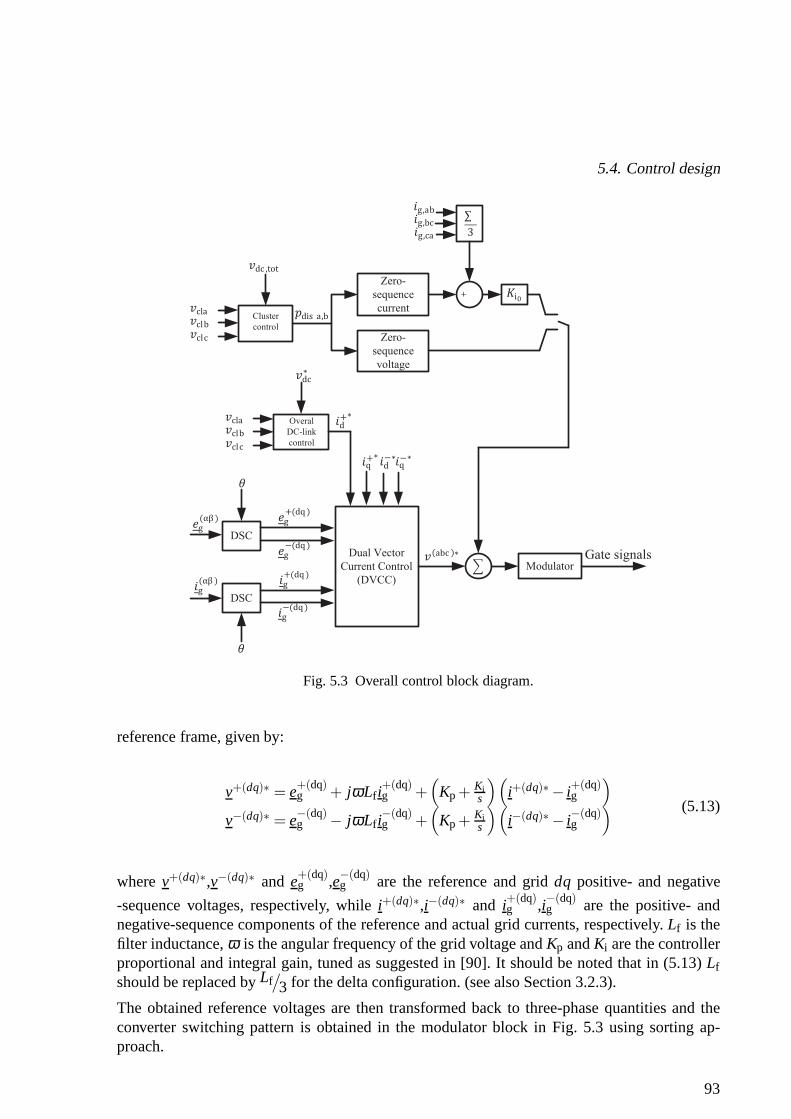
5.4. Control design
Dual Vector
Current Control
(DVCC)
DSC
DSC
ModulatorGate signals
Zero-
sequence
voltage
Zero-
sequence
current
Overal
DC-link
control
Cluster
control
+
Fig. 5.3 Overall control block diagram.
reference frame, given by:
v+(dq)∗ = e+(dq)g + jωLf i
+(dq)g +
(
Kp+Kis
)(
i+(dq)∗− i+(dq)g
)
v−(dq)∗ = e−(dq)g − jωLf i
−(dq)g +
(
Kp+Kis
)(
i−(dq)∗− i−(dq)g
) (5.13)
wherev+(dq)∗,v−(dq)∗ and e+(dq)g ,e−(dq)
g are the reference and griddq positive- and negative
-sequence voltages, respectively, whilei+(dq)∗,i−(dq)∗ and i+(dq)g ,i−(dq)
g are the positive- andnegative-sequence components of the reference and actual grid currents, respectively.Lf is thefilter inductance,ω is the angular frequency of the grid voltage andKp andKi are the controllerproportional and integral gain, tuned as suggested in [90].It should be noted that in (5.13)Lfshould be replaced byLf
/
3 for the delta configuration. (see also Section 3.2.3).
The obtained reference voltages are then transformed back to three-phase quantities and theconverter switching pattern is obtained in the modulator block in Fig. 5.3 using sorting ap-proach.
93

Chapter 5. Operation of CHB-STATCOM under unbalanced conditions
CC
Positive
sequence
CC
Negative
sequence
Gain
Fig. 5.4 Block diagram of dual vector current-controller (DVCC). θ ′ = θ and Gain=1 for star case orθ ′ = θ + π
6 and Gain=√
3 for delta case.
5.4.2 DC-link voltage control
The DC-link voltage control comprises of two stages:
1. Overall DC-link voltage control.
2. Cluster voltage (defined as the average DC-link voltage ineach phase) control.
The overall DC-link voltage control is responsible to provide sufficient power to maintain thecharge of all DC capacitors in the three phases. Using a voltage-orienteddq transformation(d-axis aligned with the grid-voltage vector) and setting thenegative-sequence active power tozero (e−gdi−gd+ e−gqi−gq = 0), the total three phase power on the AC side is equal to
ptot = e+gdi+gd (5.14)
The active power balance equation from the AC and DC side can be written as
ptot = e+gdi+gd =12
Cdc
n
[
ddt(
n
∑k=1
vadc,k)
2+ddt(
n
∑k=1
vbdc,k)
2+ddt(
n
∑k=1
vcdc,k)
2
]
=12
nCdcddt
(
n∑
k=1va
dc,k
n)2+(
n∑
k=1vb
dc,k
n)2+(
n∑
k=1vc
dc,k
n)2
=3nCdc
2ddt
[(vcla)
2+(vclb)2+(vclc)
2
3
]
(5.15)
94

5.4. Control design
Fig. 5.5 Closed-loop block diagram of the overall DC-link voltage controller.
wheren is the number of cells per phase andCdc is the DC-link capacitor. Equation (5.15) canbe written in Laplace domain as
e+gdi+gd =3n2
Cdcs
[(vcla)
2+(vclb)2+(vclc)
2
3
]
(5.16)
The active power flow is controlled through the direct component of the positive-sequence cur-rent, as [90]
i+∗d = Kov
v∗2
dc−[(vcla)
2+(vclb)2+(vclc)
2
3
]
(5.17)
whereKov is the controller gain andv∗dc is the reference value for the DC-link voltage. Using(5.16) and (5.17) and considering an ideal current regulation (i+gd = i+∗
d ), the closed-loop blockdiagram of the overall DC-link voltage controller is displayed in Fig. 5.5.
The closed-loop transfer function of the overall DC-link voltage controller is
Gov =
2Kove+gd3nCdc
s+2Kove+gd3nCdc
(5.18)
which is a low pass filter with bandwidth ofαov. The gain of the proportional controller can bedesign based on the desired bandwidth as
αov =2Kove+gd
3nCdc⇒ Kov =
αov3nCdc
2e+gd
(5.19)
The same overall DC-link controller can be used for both starand delta.
The cluster voltage control calculates the amount of zero-sequence voltage from (5.9) for thestar configuration or zero-sequence current from (5.11) forthe delta. This is here achievedthrough the control of the disturbance powerpdisa andpdisb as
pdisa= kz((vcla)
2+(vclb)2+(vclc)
2
3− v2
cla)
pdisb= kz((vcla)
2+(vclb)2+(vclc)
2
3− v2
clb)
(5.20)
95

Chapter 5. Operation of CHB-STATCOM under unbalanced conditions
Fig. 5.6 Closed-loop block diagram of the cluster voltage controller.
wherekz is a proportional gain andvcla and vclb are the cluster voltages of phasea and b,respectively. The active power equation for the cluster voltages can then be written as
12
nCdcs(v2cla) = pdisa (5.21)
where pdisa represents any disturbance that causes the cluster voltages to deviate. Replacing(5.20) into (5.21), the closed-loop block diagram of the cluster controller can be shown asFig. 5.6. The closed-loop transfer function of the cluster voltage controller is
Gz =
2KznCdc
s+ 2KznCdc
=αz
s+αz(5.22)
whereαz is the bandwidth of the cluster controller. From (5.22) the proportional gain of thecluster voltage control is given by
Kz =nCdcαz
2(5.23)
which can be used for both star and delta.
Note that the zero-sequence voltage calculated for the starconfiguration can be directly added tothe reference voltages output from the DVCC(see Fig. 5.3); for the delta configuration, instead,the zero-sequence voltage that leads to the desired currentcirculation is obtained through aproportional controller of gainKio as
vi0 = Kio
(
i0cos(θ +δi0)−(ia∆ + ib∆ + ic∆)
3
)
(5.24)
5.4.3 Simulation results
The control method is verified for both star and delta with thesystem and control parametersreported in Table 5.1. Note that, in order to preserve the number of levels between the twoconfigurations, the DC-link voltage is doubled for the star case, in order to provide enoughmargin for the zero-sequence voltage under unbalanced condition.
The overall DC-link voltage control is designed based on a fast current controller assumption.
96
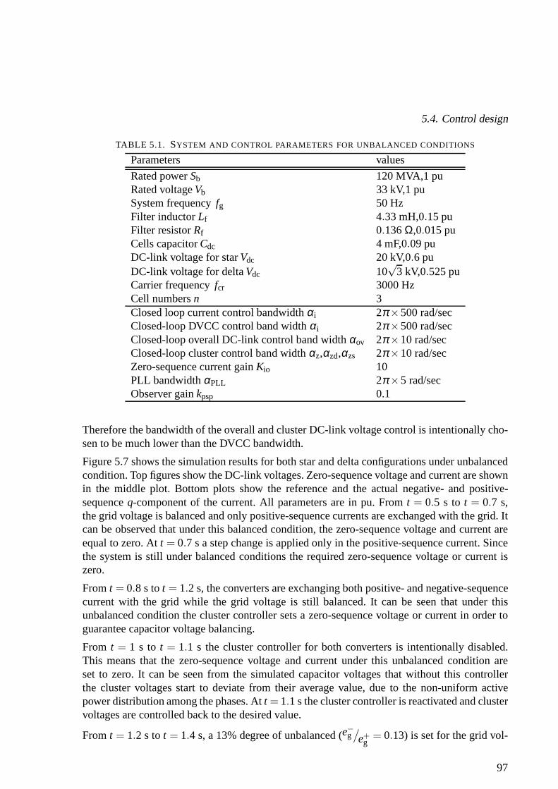
5.4. Control design
TABLE 5.1. SYSTEM AND CONTROL PARAMETERS FOR UNBALANCED CONDITIONS
Parameters values
Rated powerSb 120 MVA,1 puRated voltageVb 33 kV,1 puSystem frequencyfg 50 HzFilter inductorLf 4.33 mH,0.15 puFilter resistorRf 0.136Ω,0.015 puCells capacitorCdc 4 mF,0.09 puDC-link voltage for starVdc 20 kV,0.6 puDC-link voltage for deltaVdc 10
√3 kV,0.525 pu
Carrier frequencyfcr 3000 HzCell numbersn 3Closed loop current control bandwidthαi 2π ×500 rad/secClosed-loop DVCC control band widthαi 2π ×500 rad/secClosed-loop overall DC-link control band widthαov 2π ×10 rad/secClosed-loop cluster control band widthαz,αzd,αzs 2π ×10 rad/secZero-sequence current gainKio 10PLL bandwidthαPLL 2π ×5 rad/secObserver gainkpsp 0.1
Therefore the bandwidth of the overall and cluster DC-link voltage control is intentionally cho-sen to be much lower than the DVCC bandwidth.
Figure 5.7 shows the simulation results for both star and delta configurations under unbalancedcondition. Top figures show the DC-link voltages. Zero-sequence voltage and current are shownin the middle plot. Bottom plots show the reference and the actual negative- and positive-sequenceq-component of the current. All parameters are in pu. Fromt = 0.5 s to t = 0.7 s,the grid voltage is balanced and only positive-sequence currents are exchanged with the grid. Itcan be observed that under this balanced condition, the zero-sequence voltage and current areequal to zero. Att = 0.7 s a step change is applied only in the positive-sequence current. Sincethe system is still under balanced conditions the required zero-sequence voltage or current iszero.
Fromt = 0.8 s tot = 1.2 s, the converters are exchanging both positive- and negative-sequencecurrent with the grid while the grid voltage is still balanced. It can be seen that under thisunbalanced condition the cluster controller sets a zero-sequence voltage or current in order toguarantee capacitor voltage balancing.
From t = 1 s to t = 1.1 s the cluster controller for both converters is intentionally disabled.This means that the zero-sequence voltage and current underthis unbalanced condition areset to zero. It can be seen from the simulated capacitor voltages that without this controllerthe cluster voltages start to deviate from their average value, due to the non-uniform activepower distribution among the phases. Att = 1.1 s the cluster controller is reactivated and clustervoltages are controlled back to the desired value.
Fromt = 1.2 s tot = 1.4 s, a 13% degree of unbalanced (e−g/
e+g= 0.13) is set for the grid vol-
97

Chapter 5. Operation of CHB-STATCOM under unbalanced conditions
tage. DC-link voltage results show the ability of the cluster controller to provide an appropriatezero-sequence voltage and current to control the cluster voltages under this new unbalancedcondition.
Simulation results for the reactive component of the current are also showing the proper ope-ration of the DVCC in providing an independent negative- andpositive-sequence current con-trol; only a small cross-coupling between the sequence components, due to the dynamic perfor-mance of the implemented DSC for sequence separation, can beobserved during the simulatedcurrent steps.
Fig. 5.7 Transient responses of star and delta configurations under unbalanced condition; top: DC-linkvoltages in three phases; middle: zero-sequence voltage and current; bottom: negative- andpositive-sequenceq-component of the current.
Figure 5.8 shows the grid three-phase voltage and current from the previous simulation. Forclarity purpose, the grid three-phase voltages are shown only from t = 1.16 s tot = 1.24 s. As itmentioned earlier, att = 1.2 s 13% degree of unbalanced is applied to the grid voltage. The gridthree-phase currents are shown fromt = 0.76 s tot = 0.84 s. It was shown that untilt = 0.8 s,only positive-sequence current is exchanging between the grid and the converters. Att = 0.8 sa step change is applied to the negative-sequence current. This leads to three-phase unbalancedcurrents as can be seen in this figure.
98

5.5. Operating range of CHB-STATCOMs under unbalanced conditions
Fig. 5.8 The grid three-phase voltage and current. (Same case study as Fig. 5.7).
5.5 Operating range of CHB-STATCOMs under unbalancedconditions
5.5.1 General comparison
The comparison between the CHB-STATCOMs operating range isbased on the required zero-sequence current and voltage to guarantee capacitor balancing under unbalanced conditions.According with (5.9) and based on the variablesK3 to K6 in (5.7), it is possible to concludethat the star configuration is mainly sensitive to the amountof positive- and negative-sequencecurrents that the converter exchanges with the grid. Similarly, according with (5.11) and basedon K13 to K16 defined in (5.12), the delta configuration is sensitive to theamplitude of thepositive- and negative-sequence components of the voltageapplied at the converter terminals.
To analyse the sensitivity for these two configurations, twocase studies are here investigated;for the star configuration, it is assumed that the grid is balanced (thus, the grid voltage is onlyconstituted by a positive-sequence component) while the converter is exchanging both positive-and negative-sequence current with the grid. For simplicity of the analysis, two operating con-ditions for the converter are here considered: the two current sequences have the same phaseangle (for example, both positive- and negative-sequence currents are injected into the grid) orthe current sequences are opposite in phase (for example, positive-sequence current is injectedinto the grid while the negative-sequence is absorbed by thecompensator). In a dual situation,for the delta configuration it is assumed that the grid is unbalanced and the converter exchangesonly positive-sequence current with the grid. The phase shift between the two sequence compo-nents of the voltage depends on a number of factors, for example the grid impedance and, in caseof unbalance due to fault conditions, on the fault location;here it is assumed that the phase shiftbetween positive- and negative-sequence voltage is eitherequal to zero or toπ , in order to high-light the duality between the two configurations. It is also assumed that the filter impedancebetween the grid and converter is purely inductive and losses are neglected (δ+ = θ+ ± π
2 ).
99

Chapter 5. Operation of CHB-STATCOM under unbalanced conditions
TABLE 5.2. NEGATIVE- AND POSITIVE-SEQUENCE QUANTITIES WITH THEIR CORRESPONDING
ZERO-SEQUENCE VOLTAGE OR CURRENT
v+,θ+v v−,θ−
v i+,δ+i i−,δ−
i v0 or i0star V+,0 0,0 I+,±π
2 I−,±π2
A√3(I−2−I+2
)
star V+,0 0,0 I+,∓π2 I−,±π
2A′
√3(I−2−I+2
)
delta V+,0 V−,0 I+,±π2 0,0 B√
3(V−2−V+2)
delta V+,0 V−,π I+,±π2 0,0 B′
√3(V−2−V+2
)
Table 5.2 summarizes the different sequence components forthe considered cases. The corres-ponding zero-sequence voltage and current are calculated using (5.9) and (5.11). Other parame-ters in Table 5.2 are defined as follow
A =√
C2(I−+ I+)2+12(I−− I+)2P2disa
A′ =√
C2(I−− I+)2+12(I−+ I+)2P2disa
B =√
D2(V−+V+)2+12(V−−V+)2P2disa
B′ =√
D2(V−−V+)2+12(V−+V+)2P2disa
(5.25)
withC = 2Pdisa+4Pdisb−
√3V+I−
D = 2Pdisa+4Pdisb−√
3V−I+
The solution for the zero-sequence voltage/current shows that a practical limitation exists inboth configurations, with an infinite zero-sequence requirement needed under specific operatingconditions. In the specific, the operating range of the star configuration is limited by the degree
of unbalance (I−/
I+). From Table 5.2, it can be observed thatV0 tends to infinity when the ratioI−/
I+ approaches 1, i.e. a theoretically infinite voltage for the Y-point to allow power distribu-tion among phases when the amplitude of the exchanged negative-sequence current equals theamplitude of the positive-sequence. In practical applications, the maximum attainable outputvoltage of the converter leg will determine the maximum degree of unbalance that the convertercan cope with before losing the controllability of the DC-link voltages. Similar phenomena willappear for the delta configuration, where the operating range is limited by the degree of voltage
unbalance (V−/
V+). From Table 5.2, it can be observed that the zero-sequence currentI0 tends
to infinity when the ratio (V−/
V+) tends to 1. It is of importance to stress that the singularityis independent from the assumptions in Table 5.2 and will occur in any unbalanced condition ifthe voltage ratio for the delta and the current ratio for the star tends to 1.
Figure 5.9 (a),(c) shows the relation between positive- andnegative-sequence currents and zero-sequence voltage amplitude for the star configuration whenδ+ = δ− = π
2 (a) andδ+ =−δ− =π2 (c). For the simulated case,V+ is equal to 1 pu, whilePdisa andPdisb are set to 0.02 pu and0.01 pu, respectively. Observe thatPdisa, Pdisb are intentionally chosen to be very small, since
100

5.5. Operating range of CHB-STATCOMs under unbalanced conditions
they are just to model the small disturbances caused by non-idealities. It can be observed that inboth operating conditions, the singularity occurs whenI+ = I−. It is of interest to observe thatmore effort is needed from a balancing point of view (i.e., more zero-sequence voltage injectionfor the same amount of current unbalance) when the current positive- and negative-sequencecomponents have the same phase angle (δ+ = δ− = π
2 in Fig. 5.9(a)).
Figure 5.9 (b),(d) shows the relation between positive- andnegative-sequence voltages and zero-sequence current amplitude for the delta case whenθ+
v = θ−v = 0 (b) and whenθ+
v = 0,θ−v = π
(d). For the simulated case,I+ is equal to 1 pu, whilePdisa, Pdisb are 0.02 pu and 0.01 pu,respectively. It can be observed that in both cases the singularity occurs whenV+ =V−. Similarto the star case, more balancing effort is required whenθ+
v = θ−v = 0.
Fig. 5.9 Relationship between zero-sequence voltage/current and negative- and positive-sequence cur-rents/voltages for star/delta configurations; (a):δ+ = δ− = π
2 ; (c): δ+ = −δ− = π2 ; (b):
θ+v = θ−
v = 0; (d): θ+v = 0,θ−
v = π.
It is possible to observe from Fig. 5.9 that although star anddelta CHB-STATCOMs are sensitiveto the degree of unbalanced in the current and voltage, respectively, the required amount of zero-sequence component needed for capacitor balancing also highly depends on the relative phaseshift between the sequence components. For this reason, forthe star configuration it is of interest
101

Chapter 5. Operation of CHB-STATCOM under unbalanced conditions
[ ]
[ ]
[rad]
[rad]
Fig. 5.10 Impact of phase shift between positive- and negative-sequence component on required zero-sequence component. Top: star configuration; bottom: deltaconfiguration.
to investigate the impact of the relative phase shift between the current sequence componentson the required amount of zero-sequence voltage. Analogousinvestigation can be performedfor the delta configuration, where the impact of the relativephase shift between positive- andnegative-sequence voltage on the required zero-sequence current is investigated.
Figure 5.10, top figure, shows the required zero-sequence voltage as a function of the phaseshift between the current sequence components, denoted asξi, and the degree of unbalance inthe exchanged current. It is here assumed that the positive-sequence voltageV+ is equal to 1pu.Similar analysis is performed for the delta configuration (see Fig. 5.10, bottom figure), where theimpact of the phase shift between the negative- and the positive-sequence voltage is investigatedunder the assumption that the converter is injecting 1pu positive-sequence current into the grid.Note that the level of unbalance is limited to 0.5pu for clarity of the figure. As shown, the worstcase (i.e., highest demand on the zero-sequence component)occurs when the positive-sequencetern is aligned with the negative-sequence tern (corresponding toξi,v = 0, 2π/3, 4π/3); on thecontrary, the lowest demand on the zero-sequence componentoccurs when the two terns arein phase opposition, i.e. forξi,v = π/3, π , 5π/3. Therefore, it can be concluded that the casestudies indicated in Table I where both current sequences are in phase for the star configuration(i.e., δ+ = δ− = ±π
2 ) or when the voltage sequences are in phase for the delta configuration
102

5.5. Operating range of CHB-STATCOMs under unbalanced conditions
Fig. 5.11 Simulation results of delta configuration; (a): grid voltage; (b):v−v+ ; (c): zero-sequence current;
(d): capacitor voltages.
(θ+v = θ−
v = 0) can be seen as the worst case scenarios under the given assumptions.
In order to verify the theoretical results, simulations areperformed for the worst case scenariomentioned in Table 5.2 for both configurations, i.e.δ+ = δ− =±π
2 for the star andθ+v = θ−
v = 0for the delta.
Figure 5.11 shows the obtained simulation results for the delta configuration. Figure 5.11 (a)shows the grid voltage, figure (b) shows the degree of unbalance in the converter terminal vol-
tage (V−/
V+), figure (c) shows the zero-sequence current and figure (d) shows the capacitorvoltages in all three phases. The positive-sequence current is set to 0.5 pu.
As shown in the figure, an increase in the degree of voltage unbalance (V−/
V+) leads to anincrease of the zero-sequence current amplitude, as expected from the investigation carried out
in this section. (V−/
V+ = 1) is the critical point. If the termsPdisa andPdisb are neglected, the
amplitude of the zero-sequence current in Table 5.2 can be simplified to I+V−V−−V+ . It can be ob-
served from Fig. 5.11 that, in agreement with the theoretical analysis, for (V−/
V+ = 0.5) thezero-sequence current is about 0.5 pu and equals the amplitude of the positive-sequence current.Observe that an increase in the exchanged positive-sequence current will result in an increaseof the zero-sequence current. For example, for the considered level of voltage unbalance, a1 pu positive-sequence current would lead to a 1 pu circulating current to guarantee capacitorbalancing, meaning that the converter must have a current rating equal to 2 pu. The required cur-rent rating for the converter will further increase if the voltage unbalance is increased. Finally,
103

Chapter 5. Operation of CHB-STATCOM under unbalanced conditions
Fig. 5.12 Simulation results of star configuration; (a): line currents; (b):I−
I+ ; (c): zero-sequence voltage;(d): capacitor voltages.
Fig. 5.11 (d) clearly shows that the implemented control strategy allows proper DC-capacitorvoltage balancing.
Figure 5.12 shows the obtained simulation results for the star configuration. Figure 5.12 (a)shows the line current, figure (b) shows the degree of unbalance in the current injected by the
converter (I−/
I+), figure (c) shows the zero-sequence voltage and figure (d) shows the capa-citor voltages in all three phases. For this simulation study, the line-to-line grid voltage is setto 1 pu (corresponding to a peak value of 0.8 pu for the line-to-ground voltage) and is per-fectly balanced. As expected, an increase in the degree of unbalance in the injected current
(I−/
I+) leads to an increase in amplitude of the zero-sequence voltageV0, with a singularity
when (I−/
I+ = 1). Note that the implemented controller works properly andis able to keepthe capacitor voltages close to the reference value. As for the delta case, neglecting the termsPdisa andPdisb, from Table 5.2 the amplitude of the zero-sequence voltage can be simplified toI−V+
I−−I+ . As it can be observed from Fig. 5.12, in agreement with the theoretical calculations at
(I−/
I+ = 0.5) a 0.8 pu zero-sequence voltage peak is needed to guaranteecapacitor balancing,i.e. a voltage that is equal to the grid voltage. Therefore, for the considered case a 2 pu ratingin the converter voltage is needed to cope with the considered case. The required voltage ratingwill further increase if the current unbalance is increased.
104

5.6. Discussion
5.6 Discussion
Both theoretical and simulation results provided in this chapter show that under unbalancedconditions there is a limit in the operating range of the CHB-STATCOM, both in star and deltaconfiguration. The star configuration is sensitive to the degree of unbalance in the injectedcurrent, while the delta is sensitive to the degree of unbalance in the voltage at the converterterminals. This, together with the specific application, will dictate the selection of the suitableconfiguration for the CHB-STATCOM and its ratings.
The CHB-STATCOM is mainly used either for utility or industrial applications. Typically, therole of the compensator in utility applications is to regulate the grid voltage at the connectionpoint by aim of positive-sequence current injection. Therefore, for this kind of applications thedegree of unbalance in the injected current can be typicallyconsidered low, making the starconfiguration a suitable choice, especially when considering its reduced voltage ratings (thus,reduced number of required cascaded cells) as compared withthe delta configuration.
When a STATCOM is employed for industrial applications, instead, its aim is mainly to im-prove the power quality at the end-user interface, for example to mitigate flicker caused byarc-furnace load. Under this scenario the compensator mustbe able to exchange both negative-and positive-sequence currents with the grid and the delta configuration appears as the mostpreferable choice, especially for systems connected to relatively strong grids. However, it is ofimportance to stress that this configuration would still suffer from high zero-sequence currentrequirements in case of asymmetrical faults located in the vicinity of the grid connection point.
5.7 Conclusions
In this chapter, the effect of unbalanced voltage and current on CHB-STATCOM has been inves-tigated, both in case of star and delta configuration of the converter phase legs. Zero-sequencevoltage (for the star configuration) or current (delta) allows to maintain the DC-link voltage ofthe different cells balanced in case of unbalanced operation. However, it has been shown thatthere are special operating conditions for both the star andthe delta configuration where thezero-sequence component is unable to control the active power in each phase to zero. This is dueto a singularity that exists in the solution for the calculation of the zero-sequence components.The singularity in the delta configuration occurs when the positive- and negative-sequence com-ponents of the voltage at the converter terminals are equal,while for the star case it is governedby the equality between the positive- and the negative-sequence component of the injected cur-rent. In addition to the amplitudes, the phase angles of currents in star and voltage in delta willhighly impact the sensitivity of the converter. For the starconfiguration, the highest demand onthe zero-sequence voltage occurs when the three-phase positive-sequence currents are alignedwith the negative-sequence tern; on the contrary, the lowest demand on the zero-sequence com-ponent occurs when the two terns are in phase opposition. Analogue results hold for the deltacase. In utility applications, where the priority is on voltage regulation, the converter aims toprioritize positive-sequence current injection to boost the voltage at the connection point and atthe same time improve the degree of unbalance. Therefore, the star configuration can be utilized
105

Chapter 5. Operation of CHB-STATCOM under unbalanced conditions
for this purpose. In industrial application, such as arc furnaces, the converter aims to exchangeboth positive- and negative-sequence current; being this kind of loads typically connected torelatively strong grids, the delta configuration appears the most preferable choice for this kindof applications.
106

Chapter 6
Laboratory setup
6.1 Introduction
To validate the results obtained via simulation for the CHB-STATCOMs, the controllers havebeen tested experimentally in the Power System Laboratory at the Division of Electric PowerEngineering of Chalmers University of Technology. In this chapter, a description of the labora-tory setup and of the components used will be given. Then, obtained experimental results willbe presented.
6.2 Laboratory setup
The block diagram of the experimental setup is given in Fig. 6.1. Each phase of the converterconsists of three H-bridge cells and a filter. All three phases are connected to a delta/star switch,used to easily connect the phases either in star or in delta configuration. The converter is con-nected to an electronic AC-source that acts as the grid.
A measurement box measures the line currents and grid phase voltages and sends the signalsto the analogue input of the controller. The DC-link voltageof each cell is measured withinthe corresponding cell as a digital signal and is sent to the digital input of the controller viaoptical fibers. The controller provides the appropriated pulses for each cell and sends the pulsesto the corresponding cell via optical fibers. A figure of the actual laboratory setup is reported inFig. 6.2.
In this laboratory setup the converter is connected to a California Instrument 4500LX prog-rammable AC power source/analyzer. With this device it is possible to provide a three-phasevoltage with controllable amplitude and frequency. Control ability over the voltage amplitudemakes the start-up process much simpler since no start-up resistors and relays are needed tolimit the inrush current. All DC capacitors can be precharged slowly by gently increasing theamplitude of the AC-source voltage.
The cell boards used for this laboratory setup have been built in cooperation with Aalborg Uni-
107

Chapter 6. Laboratory setup
Filter
AC source
delta/star
switch
Current
measurment
Voltage
measurment
optical wires
DC-link
voltages
pulses
DS1006
Fig. 6.1 Block diagram of the laboratory setup.
Fig. 6.2 Picture of the laboratory setup.
108

6.2. Laboratory setup
Fig. 6.3 Picture of the cell board with DC-link capacitors.
versity, Denmark. These cells are constituted by a three-phase two-level converter PSS15S92F6-AG/PSS15S92E6-AG [91], of which only two legs are used. The DC-link consists of four 1 mFcapacitors connected in parallel. The DC-link voltage is measured within the cell board andsent to the controller via optical fibers. These boards have over/under voltage and over currentprotections. Moreover, these boards provides a 2µs hardware blanking time for the switchingsignals. The boards are also equipped with a thermal sensorsfor the semiconductors tempera-ture. The data of the cell boards are reported in Table 6.1. Figure 6.3 shows one cell board asan example.
TABLE 6.1. DATA FOR CELLS.
rated voltage 400Vrated current 8ADC-link capacitor 4mF
The control computer system consists of a PC with a DS1006 processor board. The DS1006 canbe programmed using C-code or using Matlab/Simulink. Together with the processor board, aDS2004 analogue to digital board for the analog input signals and a DS4004 for digital inputsignals are used. To generate pulse patterns, a DS5101 Digital Waveform Output Board is used.The DS5101 autonomously generates any TTL pulse patterns onup to 16 channels with highaccuracy. Since the required number of channels for this laboratory setup is more than 16, twoDS5101 boards are used and synchronized. The outputs of these boards are the firing pulseswhich are sent to each cell via optical fibers. Interrupts signals as well as board synchronizationare generated through DWO programming.
109
Chapter 6. Laboratory setup
6.3 Experimental results under balanced conditions
6.3.1 Dynamic performances of CHB-STATCOMs
A downscale version of the same model as described in Table 3.1 has been verified by experi-mental results. The system and control parameters for theseexperimental results are summa-rized in Table 6.2.
TABLE 6.2. SYSTEM AND CONTROL PARAMETERS FOR THE EXPERIMENTAL SET-UP
Parameters valuesRated powerSb 1.5 kVA,1 puRated voltageVb 173.2 V,1 puSystem frequencyfs 50 HzFilter inductorLf 15 mH,0.23 puFilter resistorRf 1.4 Ω,0.07 puCells capacitorC 4 mF,0.04 puDC-link voltage for starVDC 62 V,0.36 puDC-link voltage for deltaVDC 106 V,0.61 puCell numbersn 3Carrier frequencyfcr 1000 Hz for PS-PWM and
3000 Hz for sorting algorithmInner loop control band widthαi 2π ×500 rad/secOuter loop control band widthαcl 2π ×5 rad/secIndividual DC-link loop control band widthαind 2π ×1 rad/sec
(only for PS-PWM)PLL band widthαPLL 2π ×5 rad/secDC-link filter band widthαDC 2π ×50 rad/sec
Figure 6.4 shows the experimental results for the star connected CHB-STATCOM. The figureson the left side are the experimental results when sorting algorithm is used and the figures onthe right side are the experimental results when PS-PWM is used. Figure 6.4 (a),(e) show theDC-link voltages in all three phases, Fig. 6.4 (b),(f) show the reference and actualq-componentof the current, Fig. 6.4 (c),(g) show three phase currents and Fig. 6.4 (d),(h) show the phaseavoltage at the converter terminals. It can be observed from these experimental results that thecontroller is able to track the reference current and at the same time control all the DC-linkvoltages at the reference value.
One practical issue regarding the CHB-STATCOMs is the forward voltage drop over diodes andswitches. The effect of this voltage drop can be seen in Fig. 6.4 (d),(h). It can be observed thatthere is an asymmetry in both positive and negative peak of the voltage waveform. The reason isthat at both positive and negative peak of the voltage, the current sign is changed from positiveto negative or vice versa, due to 900 phase shift between the voltage and current in each phase.At this point the current path is changed from diodes to IGBTsor vice versa. Figure 6.5 showsthe current path and cell output voltage for positive and negative currents and when the voltagereference is positive.VD is the diode forward voltage drop,VS is the switch forward voltage
110

6.3. Experimental results under balanced conditions
drop,Vdc is the DC-link voltage andVout is the cell output voltage. It can be seen that the outputvoltage of the cell is changed once the current direction changes.
0.9 1 1.1 1.2 1.3 1.4 1.5 1.60.3
0.35
0.4
volta
ge [p
u]
star sorting algorithm(a)
0.9 1 1.1 1.2 1.3 1.4 1.5 1.6
−1
0
1
curr
ent [
pu]
(b)
1.22 1.23 1.24 1.25 1.26 1.27 1.28
−1
0
1
curr
ent [
pu]
(c)
1.45 1.46 1.47 1.48 1.49 1.5 1.51
−1
0
1
volta
ge [p
u]
Time [S]
(d)
0.9 1 1.1 1.2 1.3 1.4 1.5 1.60.3
0.35
0.4
volta
ge [p
u]
star PS−PWM(e)
0.9 1 1.1 1.2 1.3 1.4 1.5 1.6
−1
0
1
curr
ent [
pu]
(f)
1.22 1.23 1.24 1.25 1.26 1.27 1.28
−1
0
1
curr
ent [
pu]
(g)
1.45 1.46 1.47 1.48 1.49 1.5 1.51
−1
0
1
volta
ge [p
u]
Time [S]
(h)
Fig. 6.4 Experimental results of the star configuration. (a,e) DC-link voltage of all the cells, (b,f) refe-rence and actualq-current, (c,g) three-phase line currents, (d,h) converter output voltage ofphasea. Figures on the left side are with sorting algorithm and figures on the right side are withPS-PWM.
dcV+
-
DV
SV
DV
SV
outV+
-
Sdcout 2VVV
i
dcV+
-
DV
SV
DV
SV
outV+
-
Ddcout 2VVV
i
Fig. 6.5 Current path and cell output voltage.
Figure 6.6 shows the transient performance of the star configuration with and without Smithpredictor for both simulation and experimental results including the forward voltage drop ofsemiconductors in the simulation model. The figures on the left side shows the results when
111

Chapter 6. Laboratory setup
Fig. 6.6 Transient performance of the star configuration (left side are with sorting and right side are withPS-PWM) with and without Smith predictor. Figures on top aresimulation and on bottom areexperimental results.
sorting algorithm is used (simulations are on top and experimental are on bottom) the figureson the right side shows the results when PS-PWM is used (simulations are on top and experi-mental are on bottom). It can be observed that in all cases Smith predictor improves the transientperformance of the converter. Note that the asynchronous technique has been used in the im-plementation of the PS-PWM for updating the modulation indexes of each cell. It can also beobserved that there is a close similarity between the simulation and experimental results fromthe rise time and overshoot points of view. However, the experimental results show less dampingin the oscillations during the transient. This mismatch between simulation and experimental re-sults is mainly due to the dynamic behavior of the programmable AC power supply utilized inthe laboratory setup; the voltage controller of the supply together with its filtering stage that hasnot been taken into account in the simulation model, where the CHB-STATCOM is assumed tobe connected to an infinite bus.
In order to further investigate the effect of semiconductors voltage drop on the CHB-STATCOMsperformance, star configuration with the sorting algorithmis chosen as the case study. Figure 6.7shows the simulation results of the converter output voltage for phasea and its correspondingharmonic spectra. The top plot shows the results when the voltage drop over the semiconductorsis set to zero. It can be observed that the voltage waveform issymmetrical and no low-order har-monic is generated in the output voltage. The bottom plot shows the results when the forwardvoltage drop of diodes and switches are set to 2 V. The asymmetrical shapes at the positive andnegative peak of the voltage introduces low-order harmonics in the output voltage.
112

6.3. Experimental results under balanced conditions
Fig. 6.7 Converter phase voltage and its corresponding harmonic spectra; (top):without forward voltagedrop; (bottom):with voltage drop over semiconductors.
The third-order harmonic, which is the largest harmonic generated, does not affect the currentin the star configuration since the third order harmonic is eliminated in the line-to-line vol-tage. However, in the delta configuration, the third-order voltage harmonic causes a third-ordercurrent harmonic that circulates inside the delta and negatively impacts the active power distri-bution among phases. This can be considered as a large disturbance for the cluster controller inbalancing the cluster voltages.
In order to show the effect of the forward voltage drop on the cluster voltage in case of delta, thedelta configuration is simulated with and without considering the forward voltage drop and theresults are shown in Fig. 6.8. The figures on the left side are the simulation results of the clustervoltages (a), circulating current inside delta (b) and three-phase line currents (c) when 2Vforward voltage drop over the semiconductors is considered. The figures on the right side showthe same simulation results without considering any forward voltage drop. It can be observedfrom the obtained results that the forward voltage drop can have a severe effect on the clustervoltages.
To overcome this problem, the circulating current resulting from the forward voltage dropshould be controlled to zero. A simple P controller is chosenin this laboratory setup to con-trol this circulating current to zero. This controller superposes a zero-sequence voltage to thereference voltages of each phase to produce a circulating current in opposite direction of the ac-tual circulating current. This will eventually bring the total circulating current to zero. Followingequation describes the circulating current controller:
Vo∆d = ko∆d
(ia∆ + ib∆ + ic∆
3
)
(6.1)
whereVo∆d is the zero-sequence voltage correspond to the required zero sequence current,ko∆dis the proportional gain andia∆,ib∆,ic∆ are the three phase branch currents inside the delta.
Figure 6.9 shows the obtained experimental results of the delta configuration. Note that the onlydifference between the controller here and the controller explained in Chapter 3 is the extra
113

Chapter 6. Laboratory setup
1.9 1.92 1.94 1.96 1.98 20.58
0.6
0.62
0.64
volta
ge [p
u]
delta with forward voltage drop(a)
1.9 1.92 1.94 1.96 1.98 2−0.1
−0.05
0
0.05
0.1
curr
ent [
pu]
(b)
1.9 1.92 1.94 1.96 1.98 2−1
−0.5
0
0.5
1
curr
ent [
pu]
Time [S]
(c)
1.9 1.92 1.94 1.96 1.98 20.58
0.6
0.62
0.64
volta
ge [p
u]
delta without forward voltage drop(d)
1.9 1.92 1.94 1.96 1.98 2−0.1
−0.05
0
0.05
0.1
curr
ent [
pu]
(e)
1.9 1.92 1.94 1.96 1.98 2−1
−0.5
0
0.5
1
curr
ent [
pu]
Time [S]
(f)
Fig. 6.8 Simulation results of the delta configuration with and without forward voltage drop over semi-conductors; (top): cluster voltages; (middle): circulating current; (bottom) three-phase line cur-rents.
circulating current controller in (6.1). The figures on the left side are the experimental resultswhen sorting algorithm is used and the figures on the right side are the experimental resultswhen PS-PWM is used. Figure 6.9 (a),(f) show the DC-link voltages in all three phases, Fig. 6.4(b),(g) show the reference and actualq-component of the current, Fig. 6.9 (c),(h) show threephase currents, Fig. 6.9 (d),(i) show the phasea voltage of the converter and Fig. 6.9 (e),(j)show the circulating current inside delta. It can be seen that the circulating current controlleris able to keep the circulating current close to zero and thusthe converter is able to provideappropriate operation. Observe from Fig. 6.9 (a) and (f) that the cluster voltages are not exactlyequal; this is due to the fact that the circulating current controller is based on a proportionalcontroller only and therefore it is unable to set the steady-state error to zero. However, thecontroller will avoid the drifting of the DC-link voltages and keep the clusters close to theirreference values, thus allowing proper operation of the system.
Figure 6.10 shows the transient performance of the delta configuration with and without Smithpredictor for both simulation and experimental results. The figures on the left side shows theresults when sorting algorithm is used (simulations are on top and experimental are on bottom)the figures on the right side shows the results when PS-PWM is used (simulations are on top andexperimental are on bottom). Again, asynchronous technique has been used for the implemen-tation of the PS-PWM. It can be observed that there is a close similarity between the simulationand experimental results from the rise time and overshoot points of view. However, the Smithpredictor seems to be more effective in the experimental than the simulation results for the deltaconfiguration. This can be due to fact the experimental set-up has more damping terms than the
114

6.3. Experimental results under balanced conditions
Fig. 6.9 Experimental results of the delta configuration. (a,f) DC-link voltage of all the cells, (b,g) refe-rence and actualq-current, (c,h) three-phase line currents, (d,i) converter output voltage of phasea, (e,j) circulating current. Figures on the left side are with sorting algorithm and figures on theright side are with PS-PWM.
115

Chapter 6. Laboratory setup
simulation model, which in turn provides better control over the circulating current speciallyduring the transients.
Fig. 6.10 Transient performance of the delta configuration (left side are with sorting and right side arewith PS-PWM) with and without Smith predictor. Figures on top are simulation and on bottomare experimental results.
6.3.2 Integer versus non-integer carrier frequency modulation ratio
In order to validate the results regarding the use of a non-integer frequency modulation ratio, thestar configuration with PS-PWM is experimentally tested with the same frequency modulationratios used in Section 4.2.4. As shown in Section 4.2.3, the optimum carrier frequency thatleads to the least divergence in the DC-link voltages with three cells per phase is 1016.6 Hzwhen using 1000 Hz as the integer carrier frequency. Figure 6.11 shows the filtered DC-linkvoltages for the cells in phasea with different carrier frequencies of 1000 Hz (a), 1008.3 Hz(b), 1016.6 Hz (c) and 1025 Hz (d). Att = 0.5 s the individual voltage controller is inhibitedand att = 4.5 s it is activated again. It can be observed that the least divergence occurs whencarrier frequency of 1016.6 Hz is chosen, confirming the theoretical investigation.
Figure 6.12 shows the output of the individual DC-link voltage controllers for phasea whendifferent carrier frequencies are employed. Note that the individual DC-link voltage controlputs less effort in balancing the DC-link voltages in case ofnon-integer carrier frequency ratio,with minimum action when carrier frequency of 1016.6 is selected. This figure shows how
116

6.3. Experimental results under balanced conditions
1 2 3 4 50.345
0.35
0.355
volta
ge [p
u]
1000 Hz(a)
1 2 3 4 50.345
0.35
0.355
volta
ge [p
u]
1008.3 Hz(b)
1 2 3 4 50.345
0.35
0.355
volta
ge [p
u]
Time [s]
1016.6 Hz(c)
1 2 3 4 50.345
0.35
0.355
volta
ge [p
u]Time [s]
1025 Hz(d)
Fig. 6.11 Filtered DC-link voltages of phasea with different carrier frequencies and inhibited individualvoltage balancing.
the non-integer carrier frequency ratio can alleviate the role of individual balancing controller,although this control loop is still necessary when this kindof modulation strategy is adopted.
0 0.1 0.2 0.3 0.4 0.5−5
0
5x 10
−4
volta
ge [p
u]
1000 Hz(a)
0 0.1 0.2 0.3 0.4 0.5−5
0
5x 10
−4
volta
ge [p
u]
1008.3 Hz(b)
0 0.1 0.2 0.3 0.4 0.5−5
0
5x 10
−4
volta
ge [p
u]
Time [s]
1016.6 Hz(c)
0 0.1 0.2 0.3 0.4 0.5−5
0
5x 10
−4
volta
ge [p
u]
Time [s]
1025 Hz(d)
Fig. 6.12 Output of the individual DC-link voltage control for the DC-links in phasea of the star configu-ration at different carrier frequencies.
6.3.3 DC-link voltage modulation technique and zero-current mode
In Chapter 4, two methods for the individual capacitor balancing when the CHB-STATCOM isoperated at zero-current mode have been presented and investigated: the first method is basedon a modified sorting algorithm, while the second is based on the application of a modulationsignal to the DC voltage reference. However, as mentioned inthe chapter, the first methodpresents some limitations and can only be adopted when the RMS current is lower than the
117

Chapter 6. Laboratory setup
current ripple. For this reason, only the experimental results for the DC-link voltage modulationtechnique will be presented.
This technique has been implimented in the laboratory for the star configuration with the systemparameters reported in Table 6.2. Based on the system parameters, the maximum required DC-link voltage is equal as 0.354 pu. The required DC-link voltage for the zero-current mode isequal to 0.271 pu. Therefore, to keep the oscillations of theDC-link voltage between 0.271 and0.354 pu,v∗dc,0 andv in (4.28) are chosen to be 0.312 and 0.0006 pu. 5 Hz is selectedfor thefrequency of the DC-link voltage oscillations.
v∗dc[pu] =
0.312+0.0006cos(2π5t) i∗q = 0
0.354 i∗q 6= 0(6.2)
Figure 6.13 shows the obtained experimental results. The top plot shows the reference andactual reactive component of the current. The plot in the middle shows the DC-link voltages inphasea when the measured currents are used in the sorting algorithmand bottom plot shows theexperimental results when the estimated currents are used instead. The reactive current is set to1 pu untilt = 1.5 s and is then set to zero fromt = 1.5 s tot = 7.5 s and to -1 pu fromt = 7.5s tot = 8.5 s. It can be observed that when the converter starts to operate at zero-current mode,the DC-link voltage modulation technique is activated. It can also be observed that the sortingalgorithm provides a proper balancing when estimated current are used while it fails when usingthe measured currents, confirming the simulation results inSection 4.4.5.
Fig. 6.13 Experimental results of the DC-link voltages at zero-current mode using DC-link modulationtechnique; top: Reactive component of the current; middle:DC-link voltages in phasea byusing the measured currents in the sorting algorithm; bottom: DC-link voltages in phasea byusing the estimated currents in the sorting algorithm.
Observe that individual balancing is obtained with a very small value of the amplitude of theoscillations. These oscillations will have no impact on thegrid voltage.
118

6.4. Experimental results under unbalanced conditions
6.4 Experimental results under unbalanced conditions
The control method presented in Chapter 5 is verified for bothstar and delta configurationswith the control parameters of Table 6.3. System and other control parameters are the same asin Table 6.2.
TABLE 6.3. CONTROL PARAMETERS FOR UNBALANCED CONDITIONS(EXPERIMENTAL SET UP).
Parameters values
Closed loop DVCC control band widthαi 2π ×500 rad/secClosed loop overall DC-link control band widthαov 2π ×10 rad/secClosed loop cluster control band widthαz,αzd,αzs 2π ×10 rad/secZero-sequence current gainKio 30
Figure 6.14 shows the experimental results of star and deltaunder unbalanced conditions. Thegrid voltage is balanced and the converter exchanges both positive- and negative-sequence re-active current with the grid. The figures on the left side are the results for the star and thefigures on the right side are the results for the delta. All figures shows the results in per unit.Figures (a),(e) show the cluster voltages, figures (b),(f) show the positive-sequence and (c),(g)show negative-sequence currents and figures (d),(h) show the zero-sequence voltage and zero-sequence currents respectively.
Until t = 1 s both positive- and negative-sequence currents are set tozero. At t = 1 s a stepchange to one per unit in positive-sequence current is applied and att = 1.2 s a step changeto 0.1 per unit is applied in negative-sequence current. It can be observed that before applyingthe negative-sequence current very small zero-sequence voltage or current is needed to keepthe cluster voltage balanced, since the different active power between the phases is small. Afterapplying the negative-sequence current, more zero-sequence voltage or current is required tocancel out the effect of the different average active power between the phases.
It was shown previously under balanced condition that forward voltage drop over semicon-ductors produces a third order current harmonic inside the delta that impact the active powerdistribution. The same problem still exists for the unbalanced conditions, but since the con-troller for the unbalanced conditions already controls thecirculating current, it automaticallycovers the third harmonic cancellation. Perfect cluster voltage balancing shows the ability ofboth zero-sequence voltage and current in providing an evenpower distribution between thephases. In order to highlight this ability att = 1.4 s to t = 1.6 s both zero-sequence voltageand current controller are disabled. It can be observed thatonce these controllers are disabledthe cluster voltages diverge, which the reactivation of thecontrollers brings back the clustervoltages to the set point.
Following the simulation results obtained in Fig. 5.11 in Chapter 5, Fig. 6.15 shows the obtainedexperimental results for the delta configuration. Figure 6.15 (a) shows the grid voltage, figure
(b) shows the degree of unbalance in the converter terminal voltage (V−/
V+), figure (c) showsthe zero-sequence current and figure (d) shows the capacitorvoltages in all three phases. Allquantities are plotted in per unit. The positive-sequence current is set to 0.5 pu. It can be ob-served that the experimental results well match to the obtained simulation results in Chapter 5
119

Chapter 6. Laboratory setup
Fig. 6.14 Experimental results of the star (left side) and the delta (right side) configurations. (a,e) DC-link voltage of all the cells, (b,f) reference and actual positive-sequenceq-current, (c,g) refe-rence and actual negative-sequenceq-current, (d) zero-sequence voltage, (h) zero-sequencecurrent.
for the delta configuration.
Following the simulation results obtained in Fig. 5.12 in Chapter 5, Fig. 6.16 shows the obtainedexperimental results for the star configuration. Figure 6.16 (a) shows the line current, figure (b)
shows the degree of unbalance in the current injected by the converter (I−/
I+), figure (c) showsthe zero-sequence voltage and figure (d) shows the capacitorvoltages in all three phases. Forthis experimental study, the grid voltage is set to 1 pu (corresponding to a peak value of 0.8 pufor the line-to-ground voltage). Again, good match betweensimulation and experimental resultsis obtained.
6.5 Conclusions
This chapter is dedicated to the experimental results that covers the major part of the theoreticaland simulation studies of the thesis. The laboratory setup used for this experiment is intro-duced. The effect of different practical issues such as one-sample intrinsic delay in the digital
120

6.5. Conclusions
Fig. 6.15 Experimental results of the delta configuration; (a): grid voltage; (b):V−
V+ ; (c): zero-sequencecurrent; (d): capacitor voltages.
Fig. 6.16 Experimental results of the star configuration; (a): line currents; (b):I−
I+ ; (c): zero-sequencevoltage; (d): capacitor voltages.
121

Chapter 6. Laboratory setup
controller and forward voltage drop over semiconductor areshown. The close similarity be-tween the experimental results in this chapter and theoretical and simulation studies of previouschapters proves the validity of the theoretical studies in this thesis.
122

Chapter 7
Conclusions and future work
7.1 Conclusions
This thesis has dealt with the control and modulation of Cascaded H-Bridge (CHB) convertersfor STATCOM applications. With focus on the star and delta connection of the phase legs thatconstitute the converter, the system performance under balanced and unbalanced operation havebeen investigated, trying to highlight the advantages but also the challenges and possible pitfallsthat this kind of topology presents for STATCOM applications.
After an introductory overview of the main multilevel converter topologies that are availablein today’s market, the overall control structure for the CHB-STATCOM has been described inChapter 3. Guidelines for tuning of the different control loops have been presented and the dy-namic performance of the system has been tested through simulations. It has been highlightedthat in actual implementations, due to the unavoidable deviations from ideal conditions, thePhase-Shifted Pulse Width Modulation (PS-PWM) technique suffers from a non-uniform powerdistribution among the different cells that constitute thephase legs of the converter, leading tothe need for additional control loops to guarantee that the different DC-capacitor voltages do notdiverge from the reference value. The analysis of this phenomenon is carried out in Chapter 4,where it has been shown that the non-uniform active power distribution is due to the interactionbetween the carrier side-band harmonics of the cell voltageand the base-band harmonics ofthe current (when low-switching frequency for the individual cells is selected), as well as poorcancellation of the carrier side-band harmonics (mainly incase of high-switching frequency se-lection). Theoretical analysis shows that by proper selection of the frequency modulation ratio,a more even power distribution among the different cells of the same phase leg can be achieved.This selection allows to alleviate the stabilization action required from the individual balancingcontroller and thereby to enhance the overall system stability. Another technique for the indivi-dual DC-link voltage balancing discussed in Chapter 4 is thecells sorting algorithm. However, ithas been shown that both methods are not able to provide proper individual balancing when theCHB-STATCOM is not exchanging current with the grid (here denoted as zero-current mode).This condition is especially critical for the star-connected CHB-STATCOM, due to the lack ofa closed path for the current (such as in the delta configuration) to exchange energy between
123
Chapter 7. Conclusions and future work
the three phases. Two methods for individual DC-link voltage balancing at zero-current modehave been proposed and discussed. The first method is based ona modified sorting algorithm,which takes advantage of the knowledge of the current rippleduring zero-current operations,while the second method consists in superimposing a slow modulation signal to the DC-link vol-tage reference. The effectiveness of the two methods has been verified via simulation results.However, it is of importance to stress that the modified sorting approach can only be adoptedwhen the RMS current is lower than the current ripple. Furthermore, the method is sensitiveto harmonic distortion in the measured signals. This limitsthe applicability of the method toCHB-STATCOMs with low number of cascaded cells. On the otherhand, the DC-link modu-lation technique provides a simple solution, without the main limitations present in the previousmethod. Furthermore, it is of importance to stress that the introduced oscillations in the DCvoltage lead to a small active (not reactive) power flow between the converter and the grid, thusthey will not have an impact on the grid voltage. However, carefulness must be adopted whenthe converter is meant to be operated in highly distorted grids.
Chapter 5 focuses on the operation of the CHB-STATCOM under unbalanced conditions. Theneeded control modifications to allow an independent control of positive- and negative-sequencecomponents of the injected current have been discussed. Furthermore, a modification in thecluster controller to allow an uniform active power distribution between the phase legs of theconverter has been described. This includes the use of a zero-sequence voltage (for the starconfiguration) or current (delta) to control the DC-link voltages to their reference value. Theo-retical analysis has shown that regardless of the configuration utilized for the CHB-STATCOM,a singularity exists when trying to guarantee balancing in the DC-link capacitor voltages. Inparticular, it has been shown that when the phase legs of the converter are connected in star, theCHB-STATCOM is sensitive to the level of unbalance in the current exchanged with the grid,with a singularity in the solution when positive- and negative-sequence currents have the samemagnitude. Similar results have been obtained for the deltaconfiguration, where the system isfound to be sensitive to the level of unbalance in the appliedvoltage. Furthermore, these sin-gularities as well as the zero-sequence voltage/current demands around the singularity pointshighly depend on the relative phase shift between the sequence components (current for the starand voltage for the delta configuration). The presence of these singularities represents an impor-tant limit of this topology for STATCOM applications and suggests that the star configuration ismost suitable for utility applications, where the converter is mainly employed for voltage regu-lation (mainly through positive-sequence current injection); for industrial applications or, morein general, when the CHB-STATCOM is used for balancing purposes, the delta configurationis the most preferable choice. However, the converter must be over-rated in terms of currentin order to accommodate the needed circulating current. Furthermore, the dependency of thesingularity on the level of voltage unbalance can lead to difficulties in the capacitor balancingin case of unsymmetrical faults that occur in the vicinity ofthe point of common coupling. Alltheoretical findings have also been validated through experimental tests.
124

7.2. Future work
7.2 Future work
The CHB converter and more in general the modular multilevelconcept is still rather newand offers both opportunities and challenges for the researchers to improve its efficiency andperformance. One important aspect that still needs research effort is the control and modulationof the converter; today, the research community is mainly divided into two main streams: theclassical control and modulation approach, mainly based onlinear control theory combinedwith various PWM techniques, and Model Predictive Control (MPC) approach. Both directionsare of high interest and need further investigation in orderto preserve (or even increase) theperformance of the system and at the same time reduce to the minimum the number of switchingevents.
Also, the operation of the CHB-STATCOM in case of connectionto weak grids is a challenge,especially when utilized for balancing purpose. Under thisscenario, an interesting field of re-search is to investigate alternative control strategies for positive- and negative-sequence currentinjection, especially when the CHB-STATCOM is stressed andoperated close to its limits.
It has been shown in this thesis that the two main configurations for the CHB-STATCOM avai-lable in today’s market (i.e., the star and the delta configuration) present severe limitations whenoperated under unbalanced conditions. Recent standards require more and more participationfrom grid-connected converters to reduce the level of unbalance in the grid; if this is not a prob-lem for those multilevel converters that present a common DClink (such as the NPC or the CCCtopologies), the limitations in the star and delta CHB-STATCOM can be crucial and limit theapplicability of this converter topology. For this reason,it can be of high interest to investigatealternative configurations for modular multilevel STATCOMs, in order to extend its operationalrange under unbalanced conditions.
125

Chapter 7. Conclusions and future work
126

References
[1] G. Andersson, P. Donalek, R. Farmer, N. Hatziargyriou, I. Kamwa, P. Kundur, N. Mar-tins, J. Paserba, P. Pourbeik, J. Sanchez-Gasca, R. Schulz,A. Stankovic, C. Taylor, andV. Vittal, “Causes of the 2003 major grid blackouts in north america and europe, and rec-ommended means to improve system dynamic performance,”IEEE Transactions on PowerSyst., vol. 20, no. 4, pp. 1922–1928, Nov 2005.
[2] N. G. Hingorani and L. Gyugyi,Understanding FACTS: Concepts and Technology of Flex-ible AC Transmission Systems. New York: IEEE Press, 2000.
[3] X. P. Zhang, C. Rehtanz, and B. Pal,Flexible AC Transmission Systems Modelling andControl. Springer, 2006.
[4] G. F. Reed, M. Takeda, and I. Iyoda, “Improved power quality solutions using advancedsolid-state switching and static compensation technologies,” in Proc. of Power Engineer-ing Society 1999 Winter Meeting, IEEE, vol. 2, Jan 1999, pp. 1132–1137.
[5] H. Chong, A. Q. Huang, M. E. Baran, S. Bhattacharya, W. Litzenberger, L. Anderson,A. L. Johnson, and A. Edris, “Statcom impact study on the integration of a large windfarm into a weak loop power system,”IEEE Transactions on Energy Convers., vol. 23,no. 1, pp. 226–233, March 2008.
[6] C. C. Davidson and G. de Preville, “The future of high power electronics in transmissionand distribution power systems,” inProc. of 13th European Conference on Power Elec-tronics and Applications, EPE, Sept 2009, pp. 1–14.
[7] V. K. Sood,HVDC and FACTS Controllers - Applications of Static Converters in PowerSystems. Boston: Kluwer Academic Publishers, 2004.
[8] H. Akagi, S. Inoue, and T. Yoshii, “Control and performance of a transformerless cascadepwm statcom with star configuration,”IEEE Transactions on Ind. Appl.,, vol. 43, no. 4,pp. 1041–1049, July 2007.
[9] A. Lesnicar and R. Marquardt, “An innovative modular multilevel converter topology suit-able for a wide power range,” inProc. of Power Tech Conference, 2003 IEEE Bologna,vol. 3, June 2003, p. 6 pp.
127

References
[10] C. D. Townsend, S. M. Cox, A. J. Watson, T. J. Summers, R. E. Betz, and J. C. Clare,“Voltage balancing characteristics for a cascaded h-bridge multi-level statcom employingspace vector modulation,” inProc. of 15th International Power Electronics and MotionControl Conference (EPE/PEMC), Sept 2012, pp. DS3b.3–1–DS3b.3–7.
[11] K. Ilves, L. Harnefors, S. Norrga, and H.-P. Nee, “Analysis and operation of modular mul-tilevel converters with phase-shifted carrier pwm,”IEEE Transactions on Power Electron.,vol. 30, no. 1, pp. 268–283, Jan 2015.
[12] J. Yutaka Ota, Y. Shibano, and H. Akagi, “A phase-shifted pwm d-statcom using a modularmultilevel cascade converter (ssbc); part ii: Zero-voltage-ride-through capability,”IEEETransactions on Ind. Appl., vol. 51, no. 1, pp. 289–296, Jan 2015.
[13] Q. Song and W. Liu, “Control of a cascade statcom with star configuration under unba-lanced conditions,”IEEE Transactions on Power Electro., vol. 24, no. 1, pp. 45–58, Jan2009.
[14] N. Hatano and T. Ise, “Control scheme of cascaded h-bridge statcom using zero-sequencevoltage and negative-sequence current,”IEEE Transactions on Power Del., vol. 25, no. 2,pp. 543–550, April 2010.
[15] L. Tan, S. Wang, P. Wang, Y. Li, Q. Ge, H. Ren, and P. Song, “High performance controllerwith effective voltage balance regulation for a cascade statcom with star configurationunder unbalanced conditions,” inProc. of 15th European Conference on Power Electronicsand Applications (EPE), Sept 2013, pp. 1–10.
[16] M. Hagiwara, R. Maeda, and H. Akagi, “Negative-sequence reactive-power control bya pwm statcom based on a modular multilevel cascade converter (mmcc-sdbc),”IEEETransactions on Industry Appl., vol. 48, no. 2, pp. 720–729, March 2012.
[17] R. Betz, T. Summers, and T. Furney, “Symmetry compensation using a h-bridge multilevelstatcom with zero sequence injection,” inProc. of 41st Industry Applications Conference(IAS) Annual Meeting, vol. 4, Oct 2006, pp. 1724–1731.
[18] S. Du, J. Liu, J. Lin, and Y. He, “Control strategy study of statcom based on cascadedpwm h-bridge converter with delta configuration,” inProc. of 7th International PowerElectronics and Motion Control Conference (IPEMC), vol. 1, June 2012, pp. 345–350.
[19] H. Akagi, “Classification, terminology, and application of the modular multilevel cascadeconverter (mmcc),”IEEE Transactions on Power Electron.,, vol. 26, no. 11, pp. 3119–3130, Nov 2011.
[20] S. Du and J. Liu, “A brief comparision of series-connected modular topology in statcomapplication,” inProc. of ECCE Asia Downunder (ECCE Asia), 2013 IEEE, June 2013, pp.456–460.
[21] T. Wijnhoven, G. Deconinck, T. Neumann, and I. Erlich, “Control aspects of the dynamicnegative sequence current injection of type 4 wind turbines,” in Proc. of PES GeneralMeeting, Conference Exposition, IEEE, July 2014, pp. 1–5.
128

References
[22] B. R. H and B. L. H, “Electric power converter,” Feb. 18 1975, uS Patent 3,867,643.[Online]. Available: http://www.google.com/patents/US3867643
[23] J. Rodriguez, J.-S. Lai, and F. Z. Peng, “Multilevel inverters: a survey of topologies, con-trols, and applications,”IEEE Transactions on Industrial Electron.,, vol. 49, no. 4, pp.724–738, Aug 2002.
[24] J. Rodriguez, S. Bernet, B. Wu, J. Pontt, and S. Kouro, “Multilevel voltage-source-converter topologies for industrial medium-voltage drives,” IEEE Transactions on Indus-trial Electron.,, vol. 54, no. 6, pp. 2930–2945, Dec 2007.
[25] M. Malinowski, K. Gopakumar, J. Rodriguez, and M. Perez, “A survey on cascaded multi-level inverters,”IEEE Transactions on Industrial Electron.,, vol. 57, no. 7, pp. 2197–2206,July 2010.
[26] S. Kouro, M. Malinowski, K. Gopakumar, J. Pou, L. Franquelo, B. Wu, J. Rodriguez,M. Perez, and J. Leon, “Recent advances and industrial applications of multilevel conver-ters,”IEEE Transactions on Industrial Electron.,, vol. 57, no. 8, pp. 2553–2580, Aug 2010.
[27] S. Debnath, J. Qin, B. Bahrani, M. Saeedifard, and P. Barbosa, “Operation, control, andapplications of the modular multilevel converter: A review,” IEEE Transactions on PowerElectron.,, vol. 30, no. 1, pp. 37–53, Jan 2015.
[28] J. Vivas, G. Bergna, and M. Boyra, “Comparison of multilevel converter-based statcoms,”in proc. of Power Electronics and Applications (EPE 2011-ECCE Europe), Proceedingsof the 2011-14th European Conference on, Aug 2011, pp. 1–10.
[29] J. Barrena, S. Aurtenechea, J. Canales, M. Rodriguez, and L. Marroyo, “Design, analysisand comparison of multilevel topologies for dstatcom applications,” inProc. of PowerElectronics and Applications (EPE 2005-ECCE Europe), 2005 European Conference on,Sept 2005, pp. 10 pp.–P.10.
[30] D. Soto and T. Green, “A comparison of high-power converter topologies for the imple-mentation of facts controllers,”IEEE Transactions on Industrial Electron.,, vol. 49, no. 5,pp. 1072–1080, Oct 2002.
[31] J. Rodriguez, L. Franquelo, S. Kouro, J. Leon, R. Portillo, M. Prats, and M. Perez, “Mul-tilevel converters: An enabling technology for high-powerapplications,”Proceedings ofthe IEEE, vol. 97, no. 11, pp. 1786–1817, Nov 2009.
[32] A. Nabae, I. Takahashi, and H. Akagi, “A new neutral-point-clamped pwm inverter,”IEEETransactions on Ind. Appl.,, vol. IA-17, no. 5, pp. 518–523, Sept 1981.
[33] T. Bruckner, S. Bernet, and H. Guldner, “The active npc converter and its loss-balancingcontrol,” IEEE Transactions on Industrial Electron.,, vol. 52, no. 3, pp. 855–868, June2005.
129

References
[34] R. Grunbaum, A. Sannino, and C. Wahlberg, “Use of facts for enhanced flexibility and ef-ficiency in power transmission and distribution grids,” inProc. of World Energy Congress,2010 Montreal, 2010.
[35] T. Meynard and H. Foch, “Multi-level conversion: high voltage choppers and voltage-source inverters,” inProc. of Power Electronics Specialists Conference, 1992. PESC ’92Record., 23rd Annual IEEE, Jun 1992, pp. 397–403 vol.1.
[36] K. Fujii, U. Schwarzer, and R. De Doncker, “Comparison of hard-switched multi-levelinverter topologies for statcom by loss-implemented simulation and cost estimation,” inProc. of Power Electronics Specialists Conference, 2005. PESC ’05. IEEE 36th, June2005, pp. 340–346.
[37] M. Marchesoni, M. Mazzucchelli, and S. Tenconi, “A nonconventional power converterfor plasma stabilization,”IEEE Transactions on Power Electron.,, vol. 5, no. 2, pp. 212–219, Apr 1990.
[38] M. Manjrekar and T. Lipo, “A hybrid multilevel invertertopology for drive applications,”in Proc. of Applied Power Electronics Conference and Exposition, 1998. APEC, ThirteenthAnnual, vol. 2, Feb 1998, pp. 523–529.
[39] F. Z. Peng, J.-S. Lai, J. McKeever, and J. VanCoevering,“A multilevel voltage-sourceinverter with separate dc sources for static var generation,” IEEE Transactions on Ind.Appl.,, vol. 32, no. 5, pp. 1130–1138, Sep 1996.
[40] J. Munoz, P. Melın, and J. Espinoza,Static Compensators (STATCOMs) in Power Systems.Springer Singapore, 2015, ch. Control of Multilevel STATCOMs.
[41] C. Davidson and D. Trainer, “Innovative concepts for hybrid multi-level converters forhvdc power transmission,” inProc. of AC and DC Power Transmission, 2010. ACDC. 9thIET International Conference on, Oct 2010, pp. 1–5.
[42] L. Baruschka and A. Mertens, “Comparison of cascaded h-bridge and modular multilevelconverters for bess application,” inProc. of Energy Conversion Congress and Exposition(ECCE), 2011 IEEE, Sept 2011, pp. 909–916.
[43] M. Perez, S. Bernet, J. Rodriguez, S. Kouro, and R. Lizana, “Circuit topologies, modeling,control schemes, and applications of modular multilevel converters,”IEEE Transactionson Power Electro., vol. 30, no. 1, pp. 4–17, Jan 2015.
[44] A. Nami, J. Liang, F. Dijkhuizen, and G. Demetriades, “Modular multilevel converters forhvdc applications: Review on converter cells and functionalities,” IEEE Transactions onPower Electro., vol. 30, no. 1, pp. 18–36, Jan 2015.
[45] S. Agarwal and S. Deore, “Level shifted spwm of a seven level cascaded multilevel in-verter for statcom applications,” inProc. of Nascent Technologies in the Engineering Field(ICNTE), 2015 International Conference on, Jan 2015, pp. 1–7.
130

References
[46] A. Hassanpoor, S. Norrga, H. Nee, and L. Angquist, “Evaluation of different carrier-basedpwm methods for modular multilevel converters for hvdc application,” in Proc. of IECON2012 - 38th Annual Conference on IEEE Industrial Electronics Society, Oct 2012, pp.388–393.
[47] C. Zeng, D. Liu, and Q. Liao, “Simulation research of space vector pwm based on har-monic injection,” in Proc. of Industrial Electronics and Applications ICIEA 2009. 4thIEEE Conference on, May 2009, pp. 2312–2315.
[48] C. Da-peng, S. Wen-xiang, X. Hui, C. Guo-cheng, and C. Chen, “Research on zero-sequence signal of space vector modulation for three-levelneutral-point-clamped inverterbased on vector diagram partition,” inProc. of Power Electronics and Motion ControlConference IPEMC. IEEE 6th International, May 2009, pp. 1435–1439.
[49] J. Munoz, J. Rohten, J. Espinoza, P. Melin, C. Baier, andM. Rivera, “Review of currentcontrol techniques for a cascaded h-bridge statcom,” inProc. of IEEE International Con-ference on Industrial Technology (ICIT), March 2015, pp. 3085–3090.
[50] Y. Feng, X. Wang, J. Wu, and H. Zhang, “Research on the cluster current control of delta-connected cascade multilevel statcom,” inProc. of Power System Technology (POWER-CON), 2014 International Conference on, Oct 2014, pp. 2316–2321.
[51] J. Mei, Y. Ji, X. Du, T. Ma, C. Huang, and Q. Hu, “Quasi-fixed-frequency hysteresis cur-rent tracking control strategy for modular multilevel converters,”Journal of power elec-tronics, vol. 14, no. 6, pp. 1147–1156, Nov 2014.
[52] N. Marks, T. Summers, and R. Betz, “Challenges for capacitor voltage balancing in acascaded h-bridge statcom utilising finite control set model predictive control,” inProc. ofPower Engineering Conference (AUPEC), 2013 Australasian Universities, Sept 2013, pp.1–6.
[53] L. Harnefors and H. Nee, “A general algorithm for speed and position estimation of acmotors,”IEEE Transactions on Industrial Electron., vol. 47, no. 1, pp. 77–83, Feb 2000.
[54] O. Wallmark and L. Harnefors, “Sensorless control of salient pmsm drives in the transitionregion,” IEEE Transactions on Industrial Electron., vol. 53, no. 4, pp. 1179–1187, June2006.
[55] L. Angquist and M. Bongiorno, “Auto-normalizing phase-locked loop for grid-connectedconverters,” inProc. of Energy Conversion Congress and Exposition, 2009. ECCE 2009.IEEE, Sept 2009.
[56] R. Ottersten and J. Svensson, “Vector current controlled voltage source converter-deadbeatcontrol and saturation strategies,”IEEE Transactions on Power Electro., vol. 17, no. 2, pp.279–285, Mar 2002.
[57] L. Harnefors,Control of Variable Speed Drives. Vasteras, Sweden: Applied Signal Pro-cessing and Control, Dept. of Electronics, Malardalen University,2002, 2002.
131

References
[58] J. I. O. Yutaka, Y. Shibano, N. Niimura, and H. Akagi, “A phase-shifted-pwm d-statcomusing a modular multilevel cascade converter (ssbc)-;parti: Modeling, analysis, and designof current control,”IEEE Transactions on Ind. Appl., vol. 51, no. 1, pp. 279–288, Jan 2015.
[59] G. R. Walker, “Digitally-implemented naturally sampled pwm suitable for multilevel con-verter control,”IEEE Transactions on Power Electro., vol. 18, no. 6, pp. 1322–1329, Nov2003.
[60] C. Townsend, T. Summers, and R. Betz, “Impact of practical issues on the harmonic per-formance of phase-shifted modulation strategies for a cascaded h-bridge statcom,”IEEETransactions on Industrial Electron., vol. 61, no. 6, pp. 2655–2664, June 2014.
[61] M. Glinka and R. Marquardt, “A new ac/ac multilevel converter family,” IEEE Transac-tions on Industrial Electron., vol. 52, no. 3, pp. 662–669, June 2005.
[62] D. Grahame Holmes and T. Lipo,Pulse Width Modulation for Power Converters: Princi-ples and Practice. John Wiley & Sons, 2003.
[63] C. D. Townsend, “Control and modulation strategies fora multi-level h-bridge statcom,”Ph.D. dissertation, University of Newcastle, 2012.
[64] Y. Li and B. Wu, “A novel dc voltage detection technique in the chb inverter-based stat-com,” IEEE Transactions on Power Del., vol. 23, no. 3, pp. 1613–1619, July 2008.
[65] Y. Sun, J. Zhao, Z. Ji, X. Yao, and Z. Zhu, “An improved dc capacitor voltage balan-cing strategy for pwm cascaded h-bridge converter-based statcom,” inProc. of 10th IEEEPower Electronics and Drive Systems 2013 (PEDS), April 2013, pp. 1245–1250.
[66] R. Xu, Y. Yu, R. Yang, G. Wang, D. Xu, B. Li, and S. Sui, “A novel control method fortransformerless h-bridge cascaded statcom with star configuration,”IEEE Transactions onPower Electro., vol. 30, no. 3, pp. 1189–1202, March 2015.
[67] J. Barrena, L. Marroyo, M. Vidal, and J. Apraiz, “Individual voltage balancing strategy forpwm cascaded h-bridge converter-based statcom,”IEEE Transactions on Ind. Electron.,vol. 55, no. 1, pp. 21–29, Jan 2008.
[68] L. Maharjan, S. Inoue, and H. Akagi, “A transformerlessenergy storage system based ona cascade multilevel pwm converter with star configuration,” IEEE Transactions on Ind.Appl., vol. 44, no. 5, pp. 1621–1630, Sept 2008.
[69] Z. Liu, B. Liu, S. Duan, and Y. Kang, “A novel dc capacitorvoltage balance control methodfor cascade multilevel statcom,”IEEE Transactions on Power Electro., vol. 27, no. 1, pp.14–27, Jan 2012.
[70] K. Ilves, L. Harnefors, S. Norrga, and H. P. Nee, “Predictive sorting algorithm for modularmultilevel converters minimizing the spread in the submodule capacitor voltages,”IEEETransactions on Power Electro., vol. 30, no. 1, pp. 440–449, Jan 2015.
132
References
[71] J. Qin and M. Saeedifard, “Reduced switching-frequency voltage-balancing strategies formodular multilevel hvdc converters,”IEEE Transactions on Power Del., vol. 28, no. 4, pp.2403–2410, Oct 2013.
[72] H. J. Lee, J. J. Jung, and S. K. Sul, “A switching frequency reduction and a mitigationof voltage fluctuation of modular multilevel converter for hvdc,” in Proc. of 15th IEEEEnergy Conversion Congress and Exposition (ECCE), Sept 2014, pp. 483–490.
[73] A. Hassanpoor, L. Angquist, S. Norrga, K. Ilves, and A. P. Nee, “Tolerance band modu-lation methods for modular multilevel converters,”IEEE Transactions on Industrial Elec-tro., vol. 30, no. 1, pp. 311–326, Jan 2015.
[74] Q. Tu, Z. Xu, and L. Xu, “Reduced switching-frequency modulation and circulating cur-rent suppression for modular multilevel converters,”IEEE Transactions on Power Del.,vol. 26, no. 3, pp. 2009–2017, July 2011.
[75] Q. Tu and Z. Xu, “Impact of sampling frequency on harmonic distortion for modularmultilevel converter,”IEEE Transactions on Power Del., vol. 26, no. 1, pp. 298–306, Jan2011.
[76] S. Bifaretti, L. Tarisciotti, A. Watson, P. Zanchetta,A. Bellini, and J. Clare, “Distributedcommutations pulse-width modulation technique for high-power ac/dc multi-level conver-ters,”Power Electronics, IET, vol. 5, no. 6, pp. 909–919, July 2012.
[77] L. Tarisciotti, P. Zanchetta, A. Watson, S. Bifaretti,J. C. Clare, and P. W. Wheeler, “Ac-tive dc voltage balancing pwm technique for high-power cascaded multilevel converters,”IEEE Transactions on Ind. Electron., vol. 61, no. 11, pp. 6157–6167, Nov 2014.
[78] S. Fan, K. Zhang, J. Xiong, and Y. Xue, “An improved control system for modular multi-level converters with new modulation strategy and voltage balancing control,”IEEE Trans-actions on Industrial Electro., vol. 30, no. 1, pp. 358–371, Jan 2015.
[79] W. Li, L. A. Gregoire, and J. Belanger, “Modeling and control of a full-bridge modularmultilevel statcom,” inProc. of Power and Energy Society General Meeting, July 2012,pp. 1–7.
[80] M. B. deAlvarenga and J. A. Pomilio, “Voltage balancingand commutation suppressionin symmetrical cascade multilevel converters for power quality applications,”IEEE Trans-actions on Ind. Electron., vol. 61, no. 11, pp. 5996–6003, Nov 2014.
[81] C. D. Townsend, T. J. Summers, and R. E. Betz, “Phase-shifted carrier modulation tech-niques for cascaded h-bridge multilevel converters,”IEEE Transactions on Ind. Electron.,vol. 62, no. 11, pp. 6684–6696, Nov 2015.
[82] Y. Zhou, D. Jiang, P. Hu, J. Guo, Y. Liang, and Z. Lin, “A prototype of modular multilevelconverters,”IEEE Transactions on Power Electron., vol. 29, no. 7, pp. 3267–3278, July2014.
133

References
[83] J. Qin and M. Saeedifard, “Predictive control of a modular multilevel converter for a back-to-back hvdc system,”IEEE Transactions on Power Del., vol. 27, no. 3, pp. 1538–1547,July 2012.
[84] C. D. Townsend, T. J. Summers, J. Vodden, A. J. Watson, R.E. Betz, and J. C. Clare,“Optimization of switching losses and capacitor voltage ripple using model predictivecontrol of a cascaded h-bridge multilevel statcom,”IEEE Transactions on Power Electro.,vol. 28, no. 7, pp. 3077–3087, July 2013.
[85] M. Beza and M. Bongiorno, “Improved discrete current controller for grid-connected vol-tage source converters in distorted grids,” inProc. of Energy Conversion Congress andExposition (ECCE), IEEE, Sept 2012, pp. 77–84.
[86] K. Sano and M. Takasaki, “A transformerless d-statcom based on a multivoltage cascadeconverter requiring no dc sources,”IEEE Transactions on Power Electro., vol. 27, no. 6,pp. 2783–2795, June 2012.
[87] S. Du, J. Liu, J. Lin, and Y. He, “A novel dc voltage control method for statcom basedon hybrid multilevel h-bridge converter,”IEEE Transactions on Power Electro., vol. 28,no. 1, pp. 101–111, Jan 2013.
[88] R. Betz and T. Summers, “Introduction to symmetrical components and their use in stat-com applications,” University of Newcastle, Australia, School of Electrical Engineeringand Computer Science, Tech. Rep., November 2009.
[89] J. Svensson and M. B. A. Sannino, “Practical implementation of delayed signal cancella-tion method for phase-sequence separation,”IEEE Transactions on Power Del., vol. 22,no. 1, pp. 18–26, Jan 2007.
[90] L. Harnefors, M. Bongiorno, and S. Lundberg, “Input-admittance calculation and shapingfor controlled voltage-source converters,”IEEE Trans. on Ind. Electron., vol. 54, no. 6,pp. 3323–3334, Dec 2007.
[91] Dual-In-Line package intelligent power module, MITSUBISHI ELECTRIC, 2013.
134

Appendix A
Transformations for three-phase systems
A.1 Introduction
This appendix describes transformations to calculate voltage vectors from three-phase quantitiesand vice versa. Moreover, expressions of the voltage vectorboth in the fixed (αβ -) and rotating(dq-) reference frame are given in the general case of unbalanced three-phase quantities.
A.2 Transformations of three-phase quantities into vector
A three phase positive system constituted by the three quantities va(t),vb(t) andvc(t) can betransformed into a vector in a complex reference frame, usually called αβ -reference frame byapplying the following transformation
v(t) = vα + jvβ = Kab
(
va(t)+ vb(t)ej 23π + vc(t)e
j 43π)
(A.1)
where the factorKab is equal to√
3/2 or 2/
3 to ensure power or amplitude invariant transfor-mation, respectively, between the two systems. Equation (A.1) can be shown in matrix formas
[vα(t)vβ (t)
]
=C23
va(t)vb(t)vc(t)
(A.2)
where the matrixC32 is equal to
C32 = Kab
[
1 −12 −1
2
0√
32 −
√3
2
]
(A.3)
135

Chapter A. Transformations for three-phase systems
The inverse transformation, assuming no zero-sequence, i.e. va(t)+ vb(t)+ vc(t) = 0 , is givenby
va(t)vb(t)vc(t)
=C23
[vα(t)vβ (t)
]
(A.4)
whereC23 is equal to
C23 =1
Kab
23 0−1
31√3
−13 − 1√
3
(A.5)
A.2.1 Transformations between fixed and rotating coordinate systems
Let the vectorv(t) rotates in theαβ -reference frame with the angular frequency ofω(t) in thepositive (counter-clockwise) direction. Let also adq-frame rotates in the same direction withthe same angular frequency. In such a case, the vectorv(t) appears as a fixed vector in thedq-frame. The components ofv(t) in thedq-frame are thus given by the projections of the vectorv(t) on thed-axis andq-axis of thedq-frame as shown in Fig. A.1.
d q
(t)
Fig. A.1 Relation betweenαβ -frame anddq-frame.
The transformation can be written in vector form as
v(dq)(t) = v(αβ )(t)e−jθ (t) (A.6)
with the angleθ(t) in Fig. A.1 given by
θ(t) = θ0+
t∫
0
ω(τ)dτ (A.7)
136

A.3. Voltage vectors for unbalanced conditions
The inverse transformation, from the rotatingdq-frame to the fixedαβ -frame is defined by
v(αβ )(t) = v(dq)(t)ejθ (t) (A.8)
The transformation between thedq- andαβ -frames can be written in matrix form as
[vd(t)vq(t)
]
= R(−θ(t))[
vα(t)vβ (t)
]
(A.9)
which is the transformation from the fixedαβ -frame to thedq-frame and
[vα(t)vβ (t)
]
= R(θ(t))[
vd(t)vq(t)
]
(A.10)
which is the transformation from the thedq-frame to the fixedαβ -frame. The projection matrixR(θ(t)) is
R(θ(t)) =[
cos(θ(t)) −sin(θ(t))sin(θ(t)) cos(θ(t))
]
(A.11)
A.3 Voltage vectors for unbalanced conditions
Let consider the following phase voltages for a three-phasesystem
va(t) = va(t)cos(ωt −ϕa)
vb(t) = vb(t)cos(ωt −ϕb− 23π)
vc(t) = vc(t)cos(ωt −ϕc− 43π)
(A.12)
where ˆva(t) andϕa are the amplitude and phase angle of phase voltageva(t), vb(t) andϕb arethe amplitude and phase angle of phase voltagevb(t), vc(t) andϕc are the amplitude and phaseangle of phase voltagevc(t), while ω is the angular frequency of the system.
Any unbalanced condition leads to unequal voltage amplitude or phase angle of the three phases.In such condition, the resulting voltage vectorvαβ (t) in the fixedαβ -frame can be expressed asthe sum of two vectors rotating in opposite directions and interpreted as positive- and negative-sequence component vectors.
vαβ (t) = E+ej(ωt+ϕ+)+E−e−j(ωt+ϕ−) (A.13)
whereE+ andE− are the amplitude of the positive and negative voltage vectors, respectively,and the corresponding phase angles are denoted byϕ+ andϕ−.
137

Chapter A. Transformations for three-phase systems
When transforming the voltage vectorvαβ from the fixedαβ -frame to the rotatingdq-frame,two rotating frame can be used, accordingly. These two frames are called positive and negativesynchronous reference frames (SRFs) and are denoted asdqp− anddqn−frame: the positiveSRF rotates counterclockwise with the angular frequency ofω, while the negative SRF rotatesclockwise with the same frequency. These two frames can be defined by the following transfor-mations
vdqp(t) = e−jθ (t)vαβ (t)
vdqn(t) = ejθ (t)vαβ (t)(A.14)
Dividing the two equations in Eq. (A.14) leads to
vdqp(t)
vdqn(t)= e−j2θ (t) ⇒ vdqp(t) = vdqn(t)e
−j2θ (t) (A.15)
According to Eq. (A.15), considering the positive-sequence component as a DC-component(zero frequency) in the positive SRF, the negative-sequence component will be a vector thatrotates with 100 Hz clockwise in the positive SRF. An analogues relation can be derived for apositive-sequence component in the negative SRF.
138

Appendix B
Symmetrical component basics
B.1 Introduction
This appendix describes the symmetrical component basics and shows how to extract the po-sitive and negative and zero sequences from a set of three-phase unbalanced voltage and viceversa.
B.2 Positive, negative and zero sequence extraction
Figure B.1 shows three sets of phase vectors. The positive sequence is defined by
v+a =V+cos(ωt)
v+b =V+cos(ωt − 23π)
v+c =V+cos(ωt − 43π)
(B.1)
The negative sequence is defined as follow:
v−a =V−cos(ωt +θ−)
v−b =V−cos(ωt +θ−− 43π)
v−c =V−cos(ωt +θ−− 23π)
(B.2)
and the zero sequence is defined as:
139

Chapter B. Symmetrical component basics
Fig. B.1 Positive, Negative and zero sequence components for a three phase unbalanced system.
v0a =V 0cos(ωt +θ0)
v0b =V 0cos(ωt +θ0)
v0c =V 0cos(ωt +θ0)
(B.3)
The time domain expressions can also be expressed in phasorsform. Positive sequence phasorsare
~V+a =V+ej0
~V+b =V+e−j 2
3π
~V+c =V+e−j 4
3π
(B.4)
the negative sequence phasors are
~V−a =V−ejθ n
~V−b =V−e(θ n−j 4
3π)
~V−c =V−e(θ n−j 2
3π)
(B.5)
and finally the zero sequence phasors are
~V 0a =V 0ejθ0
~V 0b =V 0eθ0
~V 0c =V 0eθ0
(B.6)
140

B.2. Positive, negative and zero sequence extraction
Concerning now a set of unbalanced three-phase voltage phasor as~Va,~Vb and~Vc, according tosymmetrical component theory these phasors can be written as:
~Va =~V+a +~V−
a +~V 0a
~Vb =~V+b +~V−
b +~V 0b
~Vc =~V+c +~V−
c +~V 0c
(B.7)
In order to extract the positive, negative and zero sequencecomponent phasor operatora isdefined as
a = ej 23π (B.8)
operations on thea phasor are shown in Fig. B.2.
a -
-
Fig. B.2 Operations on thea operator.
Using the phasor operatora defined in Eq. (B.8), the positive, negative and zero sequence phasordefined in Eq. (B.4)-(B.6) can be written as
V+b = a2V+
a
V+c = aV+
a
V−b = aV−
a
V−c = a2V−
a
V 0b =V 0
a
V 0c =V 0
a
(B.9)
Substituting Eq. (B.9) into Eq. (B.7) yields
141

Chapter B. Symmetrical component basics
~Va=~V+a +~V−
a +~V 0a
~Vb =~V+b +~V−
b +~V 0b = a2V+
a +aV−a +V 0
a
~Vc =~V+c +~V−
c +~V 0c = aV+
a +a2V−a +V 0
a
(B.10)
The expression can be shown in matrix form as
~Va~Vb~Vc
=
1 1 11 a2 a1 a a2
~V 0a
~V+a
~V−a
(B.11)
denoting:
B =
1 1 11 a2 a1 a a2
(B.12)
Inverse matrix ofB can be shown as
B−1 =13
1 1 11 a a2
1 a2 a
(B.13)
Using the inverse matrix ofB the symmetrical positive,negative and zero sequence componentsin terms of the phase voltages can be written as follow
~V 0a
~V+a
~V−a
=13
1 1 11 a a2
1 a2 a
~Va~Vb~Vc
(B.14)
substituting Eq. (B.14) into Eq. (B.9) and after some manipulation the following expressions canbe obtained for all the symmetrical component sequences from the unbalanced phase voltages.The positive sequence can be expressed as
~V+a
~V+b
~V+c
=13
1 a a2
a2 1 aa a2 1
~Va~Vb~Vc
(B.15)
The negative sequence can be expressed as
~V−a
~V−b
~V−c
=13
1 a2 aa 1 a2
a2 a 1
~Va~Vb~Vc
(B.16)
142

B.2. Positive, negative and zero sequence extraction
The zero sequence can be expressed as
~V 0a
~V 0b
~V 0c
=13
1 1 11 1 11 1 1
~Va~Vb~Vc
(B.17)
It should be noted that the theory explained in this appendixis based on phase voltage. However,the same theory is also valid for line-to-line voltages without any modification.
143

Chapter B. Symmetrical component basics
144