opa454 high-voltage (100v), high-current (50ma
TRANSCRIPT

1FEATURES DESCRIPTION
APPLICATIONS
OPA454
V-
V+
Status
Flag
Enable/Disable Common
(E/D Com)
Enable/Disable (E/D)
+IN
-IN
VO
OPA454
SBOS391–DECEMBER 2007
High-Voltage (100V), High-Current (50mA)OPERATIONAL AMPLIFIERS, G = 1 Stable
23• WIDE POWER-SUPPLY RANGE: The OPA454 is a low-cost operational amplifier with±5V (10V) to ±50V (100V) high voltage (100V) and relatively high current drive
(25mA). It is unity-gain stable and has a• HIGH OUTPUT LOAD DRIVE: IO > ±50mAgain-bandwidth product of 2.5MHz.• WIDE OUTPUT VOLTAGE SWING: 1V to RailsThe OPA454 is internally protected against• INDEPENDENT OUTPUT DISABLE ORover-temperature conditions and current overloads. ItSHUTDOWNis fully specified to perform over a wide power-supply
• WIDE TEMPERATURE RANGE: –40°C to +85°C range of ±5V to ±50V or on a single supply of 10V to• PACKAGES: SO and HSOP PowerPAD™ 100V. The status flag is an open-drain output that
allows it to be easily referenced to standardlow-voltage logic circuitry. This high-voltage op ampprovides excellent accuracy, wide output swing, and• TEST EQUIPMENTis free from phase inversion problems that are often• AVALANCHE PHOTODIODE: found in similar amplifiers.High-V Current SenseThe output can be independently disabled using the• PIEZOELECTRIC CELLSEnable/Disable Pin that has its own common return• TRANSDUCER DRIVERS pin to allow easy interface to low-voltage logic
• SERVO DRIVERS circuitry. This disable is accomplished without• AUDIO AMPLIFIERS disturbing the input signal path, not only saving power
but also protecting the load.• HIGH-VOLTAGE COMPLIANCE CURRENTSOURCES Featured in a small exposed metal pad package, the
• GENERAL HIGH-VOLTAGE OPA454 is easy to heatsink over the extendedREGULATORS/POWER industrial temperature range, –40°C to +85°C.
Table 1. OPA454 RELATED PRODUCTSPRODUCT DESCRIPTIONOPA445 (1) 80V, 15mA
OPA452 80V, 50mAOPA547 60V, 750mAOPA548 60V, 3AOPA549 60V, 9AOPA551 60V, 200mAOPA567 5V, 2AOPA569 5V, 2.4A
(1) The OPA445 is pin-compatible with the OPA445, except inapplications using the offset trim, and NC pins other thanopen.
1
Please be aware that an important notice concerning availability, standard warranty, and use in critical applications ofTexas Instruments semiconductor products and disclaimers thereto appears at the end of this data sheet.
2PowerPAD is a trademark of Texas Instruments, Inc.3All other trademarks are the property of their respective owners.
PRODUCTION DATA information is current as of publication date. Copyright © 2007, Texas Instruments IncorporatedProducts conform to specifications per the terms of the TexasInstruments standard warranty. Production processing does notnecessarily include testing of all parameters.

www.ti.com
ABSOLUTE MAXIMUM RATINGS (1)
PIN ASSIGNMENTS
1
2
3
4
8
7
6
5
E/D (Enable/Disable)
V+
OUT
Status Flag
E/D Com (Enable/Disable Common)
-IN
+IN
V-
PowerPAD
Heat Sink
(Located on
bottom side)
(1)V-
NC(3)
NC(3)
V-
+IN
NC(3)
-IN
NC(3)
E/D Com (Enable/Disable Common)
V-
V-
NC(3)
NC(3)
Status Flag
VOUT
V+
NC(3)
NC(3)
E/D (Enable/Disable)
V-
1
2
3
4
5
6
7
8
9
10
20
19
18
17
16
15
14
13
12
11
PowerPAD
Heat Sink
(Located on
top side)
(2)
OPA454
SBOS391–DECEMBER 2007
This integrated circuit can be damaged by ESD. Texas Instruments recommends that all integrated circuits be handled withappropriate precautions. Failure to observe proper handling and installation procedures can cause damage.
ESD damage can range from subtle performance degradation to complete device failure. Precision integrated circuits may be moresusceptible to damage because very small parametric changes could cause the device not to meet its published specifications.
ORDERING INFORMATION (1)
PRODUCT PACKAGE-LEAD PACKAGE DESIGNATOR PACKAGE MARKINGOPA454 SO-8 DDA OPA454OPA454 HSOP-20 (2) DWD OPA454
(1) For the most current package and ordering information see the Package Option Addendum at the end of this document, or see the TIweb site at www.ti.com.
(2) Available Q2, 2008.
OPA454 UNITSupply Voltage VS = (V+) – (V–) 120 VSignal Input Terminals, Voltage (2) (V–) – 0.3 to (V+) + 0.3 VSignal Input Terminals, Current (2) ±10 mAE/D to E/D Com Voltage +5.5 VOutput Short-Circuit (3) ISC ContinuousOperating Temperature TJ –55 to +125 °CStorage Temperature –55 to +125 °CJunction Temperature TJ +150 °C
Human Body Model (HBM) 4000 VESD Rating: Charged Device Model (CDM) 500 V
Machine Model (MM) 150 V
(1) Stresses above these ratings may cause permanent damage. Exposure to absolute maximum conditions for extended periods maydegrade device reliability. These are stress ratings only, and functional operation of the device at these or any other conditions beyondthose specified is not implied.
(2) Input terminals are diode-clamped to the power-supply rails. Input signals that can swing more than 0.3V beyond the supply rails shouldbe current limited to 10mA or less.
(3) Short-circuit to ground.
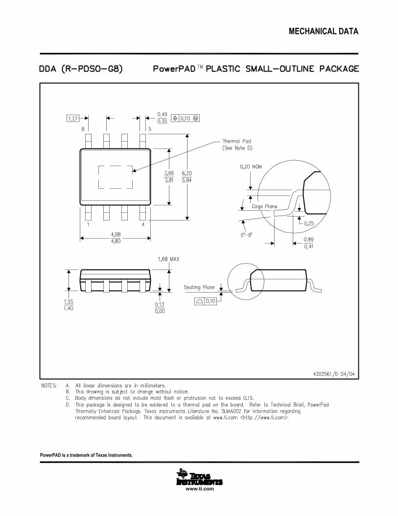
DDA PACKAGE DWD PACKAGE(1)SO-8 PowerPAD HSOP-20 PowerPAD
(TOP VIEW) (TOP VIEW)
(1) PowerPAD is internally connected to V–.Soldering the PowerPAD to the PCB isalways required, even with applications thathave low power dissipation.
(1) Available Q2, 2008.(2) PowerPAD is internally connected to V–.(3) NC = No internal connection
2 Submit Documentation Feedback Copyright © 2007, Texas Instruments Incorporated
Product Folder Link(s): OPA454

www.ti.com
ELECTRICAL CHARACTERISTICS: VS = ±50V
OPA454
SBOS391–DECEMBER 2007
Boldface limits apply over the specified temperature range, TA = –40°C to +85°C.At TP
(1) = +25°C, RL = 4.8kΩ to mid-supply, VCM = VOUT = mid-supply, unless otherwise noted.OPA454
PARAMETER CONDITIONS MIN TYP MAX UNIT
OFFSET VOLTAGE
Input Offset Voltage VOS IO = 0 ±0.2 ±4 mV
vs Temperature (2) dVOS/dT ±1.6 ±10 µV/°C
vs Power Supply PSRR VS = ±4V to ±60V, VCM = 0V 25 100 µV/V
INPUT BIAS CURRENT
Input Bias Current IB ±1.4 ±100 pA
vs Temperature See Typical Characteristics
Input Offset Current IOS ±0.2 ±100 pA
NOISE
Input Voltage Noise Density, f = 10Hz en 300 nV/√Hz
Input Voltage Noise Density, f = 10kHz 35 nV/√Hz
f = 0.01Hz to 10Hz 15 µVPP
Current Noise Density, f = 1kHz in 40 fA/√Hz
INPUT VOLTAGE RANGE
Common-Mode Voltage Range VCM Linear Operation (V–) + 2.5 See Note (3) (V+) – 2.5 V
Common-Mode Rejection CMRR VS = ±50V, –25V ≤ VCM ≤ +25V 100 146 dB
VS = ±50V, –45V ≤ VCM ≤ +45V 100 147 dB
Over Temperature VS = ±50V, –25V ≤ VCM ≤ +25V 80 88 dB
Over Temperature VS = ±50V, –45V ≤ VCM ≤ +45V 72 82 dB
INPUT IMPEDANCE
Differential Ω || pF1013 || 10
Common-Mode Ω || pF1013 || 9
OPEN-LOOP GAIN
Open-Loop Voltage Gain (4) AOL
(V–) + 1V < VO < (V+) – 1V, 100 130 dBRL = 49kΩ, IO = ±1mA
(V–) + 1V < VO < (V+) – 1V, 112 dBRL = 49kΩ, IO = ±1mA
(V–) + 1V < VO < (V+) – 2V, 100 115 dBRL = 4.8kΩ, IO = ±10mA
(V–) + 1V < VO < (V+) – 2V, 106 dBRL = 4.8kΩ, IO = ±10mA
(V–) + 2V < VO < (V+) – 3V, 80 102 dBRL = 1880Ω, IO = ±25mA
(V–) + 2V < VO < (V+) – 3V, 84 dBRL = 1880Ω, IO = ±25mA
(1) TP is the temperature of the leadframe die pad (exposed thermal pad) of the PowerPAD package.(2) See typical characteristic curve, Offset Voltage Drift Production Distribution (Figure 14).(3) Typical range is (V–) + 1.5V to (V+) – 1.5V.(4) Measured using low-frequency (<10Hz) ±49V square wave. See typical characteristic curve, Current Limit vs Temperature (Figure 24).
Copyright © 2007, Texas Instruments Incorporated Submit Documentation Feedback 3
Product Folder Link(s): OPA454
www.ti.com
OPA454
SBOS391–DECEMBER 2007
ELECTRICAL CHARACTERISTICS: VS = ±50V (continued)Boldface limits apply over the specified temperature range, TA = –40°C to +85°C.At TP = +25°C, RL = 4.8kΩ to mid-supply, VCM = VOUT = mid-supply, unless otherwise noted.
OPA454
PARAMETER CONDITIONS MIN TYP MAX UNIT
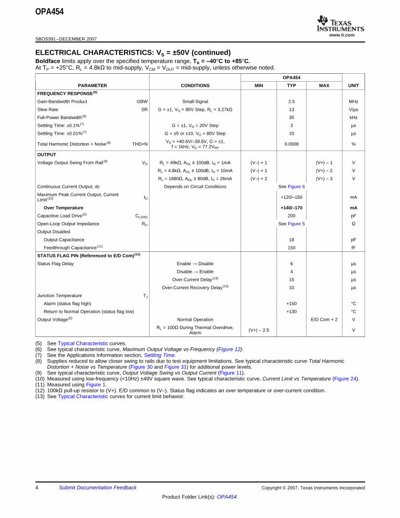
FREQUENCY RESPONSE (5)
Gain-Bandwidth Product GBW Small-Signal 2.5 MHz
Slew Rate SR G = ±1, VO = 80V Step, RL = 3.27kΩ 13 V/µs
Full-Power Bandwidth (6) 35 kHz
Settling Time: ±0.1% (7) G = ±1, VO = 20V Step 3 µs
Settling Time: ±0.01% (7) G = ±5 or ±10, VO = 80V Step 10 µs
VS = +40.6V/–39.6V, G = ±1,Total Harmonic Distortion + Noise (8) THD+N 0.0008 %f = 1kHz, VO = 77.2VPP
OUTPUT
Voltage Output Swing From Rail (9) VO RL = 49kΩ, AOL ≥ 100dB, IO = 1mA (V–) + 1 (V+) – 1 V
RL = 4.8kΩ, AOL ≥ 100dB, IO = 10mA (V–) + 1 (V+) – 2 V
RL = 1880Ω, AOL ≥ 80dB, IO = 26mA (V–) + 2 (V+) – 3 V
Continuous Current Output, dc Depends on Circuit Conditions See Figure 6
Maximum Peak Current Output, Current IO +120/–150 mALimit (10)
Over Temperature +140/–170 mA
Capacitive Load Drive (5) CLOAD 200 pF
Open-Loop Output Impedance RO See Figure 5 Ω
Output Disabled
Output Capacitance 18 pF
Feedthrough Capacitance (11) 150 fF
STATUS FLAG PIN (Referenced to E/D Com) (12)
Status Flag Delay Enable → Disable 6 µs
Disable → Enable 4 µs
Over-Current Delay (13) 15 µs
Over-Current Recovery Delay (13) 10 µs
Junction Temperature TJ
Alarm (status flag high) +150 °C
Return to Normal Operation (status flag low) +130 °C
Output Voltage (5) Normal Operation E/D Com + 2 V
RL = 100Ω During Thermal Overdrive, (V+) – 2.5 VAlarm
(5) See Typical Characteristic curves.(6) See typical characteristic curve, Maximum Output Voltage vs Frequency (Figure 12).(7) See the Applications Information section, Settling Time.(8) Supplies reduced to allow closer swing to rails due to test equipment limitations. See typical characteristic curve Total Harmonic
Distortion + Noise vs Temperature (Figure 30 and Figure 31) for additional power levels.(9) See typical characteristic curve, Output Voltage Swing vs Output Current (Figure 11).(10) Measured using low-frequency (<10Hz) ±49V square wave. See typical characteristic curve, Current Limit vs Temperature (Figure 24).(11) Measured using Figure 1.(12) 100kΩ pull-up resistor to (V+). E/D common to (V–). Status flag indicates an over temperature or over-current condition.(13) See Typical Characteristic curves for current limit behavior.
4 Submit Documentation Feedback Copyright © 2007, Texas Instruments Incorporated
Product Folder Link(s): OPA454

www.ti.com
RL
50kW
100VPP
10kHz
+50V
E/D Com
E/D
-50V
VOUT
OPA454
SBOS391–DECEMBER 2007
ELECTRICAL CHARACTERISTICS: VS = ±50V (continued)Boldface limits apply over the specified temperature range, TA = –40°C to +85°C.At TP = +25°C, RL = 4.8kΩ to mid-supply, VCM = VOUT = mid-supply, unless otherwise noted.
OPA454
PARAMETER CONDITIONS MIN TYP MAX UNIT
E/D (ENABLE/DISABLE) PIN
E/D Pin, Referenced to E/D Com Pin (14) (15)
High (output enabled) VSD Pin Open or Forced High E/D Com + 2.5 E/D Com + 5 V
E/D Com +Low (output disabled) VSD Pin Forced Low E/D Com V0.65
Output Disable Time 4 µs
Output Enable Time 3 µs
E/D COM PIN
Voltage Range (V–) (V+) – 5 V
POWER SUPPLY
Specified Range VS ±50 V
Operating Voltage Range ±5 ±50 V
Quiescent Current IQ IO = 0 3.2 4 mA
Quiescent Current in Shutdown Mode IO = 0, VE/D = 0.65V 150 210 µA
TEMPERATURE RANGE
Specified Range TA –40 +85 °C
Operating Range TA –55 +125 °C
Thermal Resistance, Junction-to-Case (16)
SO-8 PowerPAD (17) θJC 10 °C/W
HSOP-20 10 °C/W
Thermal Resistance, Junction-to-Ambient θJA
SO-8 PowerPAD (17) 24/52 °C/W
HSOP-20 (18) 65 °C/W
(14) See typical characteristic curve, IENABLE vs VENABLE (Figure 46).(15) High enables the outputs.(16) TP is the temperature of the leadframe die pad (exposed thermal pad) of the PowerPAD package.(17) Lower value is for land area of 1-inch × 1-inch, 2-oz copper. Upper value is for exposed-pad sized area of 1-oz copper.(18) Value given is for DW-20 package, similar to the DWD package, but without an exposed pad. Actual θJA may approach θJC by selection
of external heatsink and airflow.
Figure 1. Feedthrough Capacitance Circuit
Copyright © 2007, Texas Instruments Incorporated Submit Documentation Feedback 5
Product Folder Link(s): OPA454
www.ti.com
TYPICAL CHARACTERISTICS
0.1 1 10 100 1k 10k 100k 1M 10M
Frequency (Hz)
180
160
140
120
100
80
60
40
20
0
-20
Open-L
oop G
ain
, P
hase (
dB
,)
°
RLOAD = 4.87kW
C = 50pF
V = 0VLOAD
CM
Phase
Gain
-75 0-50 -25 50 75 100 125
Exposed Thermal Pad Temperature ( C)°
70
65
60
55
50
45
40
Phase M
arg
in (
)°
25
C = 200pFL
C = 30pFL
C = 100pFL
V = 0VCM
VCM = -45V
V = +45VCM
-75 0-50 -25 50 75 100 125
Exposed Thermal Pad Temperature ( C)°
3.8
3.6
3.4
3.2
3.0
2.2
2.0
Bandw
idth
(M
Hz)
25
C = 30pF. 100pF, and 200pFL
V = 45VCM
V = 45V-CM
V = 0VCM
2.8
2.6
2.4
1 1k10 100 100k 1M 10M
Frequency (Hz)
1M
100k
10k
1k
100
1
Open-L
oop O
utp
ut Im
pedance (
)W
10k
10
0 5 10 15 20 25
Peak I (mA)L
140
130
120
110
100
90
80
70
60
A(d
B)
OL
VS = ±50V
VS = ±15V
VS = ±4V
-75 -50 -25 0 25 50 75 100 125
Exposed Thermal Pad Temperature ( C)°
140
130
120
110
100
90
80
70
60
50
A(d
B)
OL
R = 48kWLOADV = 49V (dc)±OUTI = 1mA±OUT
R = 1.88kWLVOUT = +47V, -48V (dc)I = 25mA±OUT
R = 900WLV , 47V (dc)-OUT = +45VI = 50mA to 52mAOUT -
R = 4.8kWL
OUT
OUT
V = +48V, 49V (dc)
I = +9.9mA to 10mA
-
-
OPA454
SBOS391–DECEMBER 2007
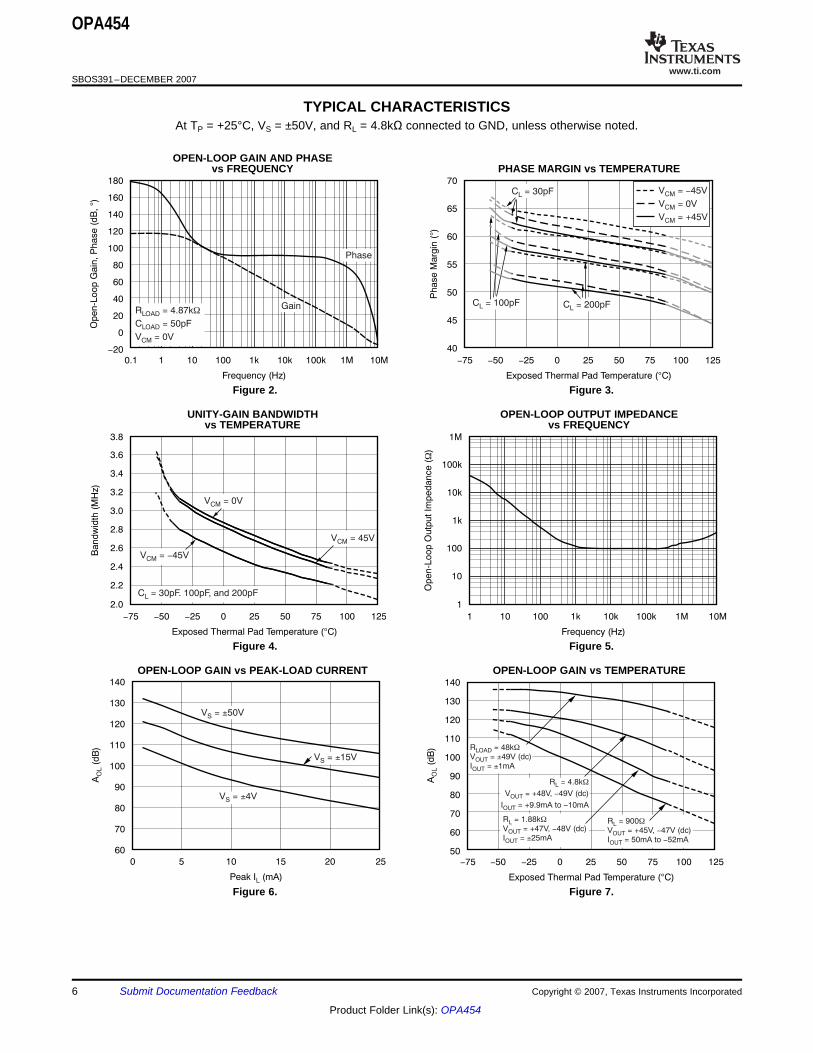
At TP = +25°C, VS = ±50V, and RL = 4.8kΩ connected to GND, unless otherwise noted.
OPEN-LOOP GAIN AND PHASEvs FREQUENCY PHASE MARGIN vs TEMPERATURE
Figure 2. Figure 3.
UNITY-GAIN BANDWIDTH OPEN-LOOP OUTPUT IMPEDANCEvs TEMPERATURE vs FREQUENCY
Figure 4. Figure 5.
OPEN-LOOP GAIN vs PEAK-LOAD CURRENT OPEN-LOOP GAIN vs TEMPERATURE
Figure 6. Figure 7.
6 Submit Documentation Feedback Copyright © 2007, Texas Instruments Incorporated
Product Folder Link(s): OPA454

www.ti.com
0.001 0.01 0.1 1 10 100 1k 10k
Frequency (Hz)
140
120
100
80
60
40
20
0
CM
RR
(dB
)
VCM = -45V
V = +45VCM
-75 -50 -25 0 25 50 75 100 125
Exposed Thermal Pad Temperature ( C)°
120
100
80
60
40
20
0
PS
RR
and C
MR
R (
dB
) 1kHz, CMRR
10kHz, CMRR
100kHz, CMRR
1.3MHz, CMRR
V = +45VCM
VCM = -45V
PSRR
1 10 100 1k 10k 100k 1M
Frequency (Hz)
140
120
100
80
60
40
20
0
PS
RR
(dB
)
50
49
48
47
-47
-48
-49
-50
0 10 20 30 40 50
I (mA)OUT
V(V
)O
UT +125 C°
- °55 C
- °55 C
+25 C°+85 C°
0 15050 100 200 300
Frequency (kHz)
120
100
80
60
40
20
0
Outp
ut V
oltage (
V)
PP
250
V = 49V
R = 4.8k
I = 10mA
OUT
L
OUT
±
W
±
Offset Voltage ( V)m
Popula
tion
-4000 -3000 -2000 40003000200010000-1000
Average = 111 V
Standard Deviation = 142 V
m
m
OPA454
SBOS391–DECEMBER 2007
TYPICAL CHARACTERISTICS (continued)At TP = +25°C, VS = ±50V, and RL = 4.8kΩ connected to GND, unless otherwise noted.
POWER-SUPPLY AND COMMON-MODECOMMON-MODE REJECTION RATIO vs FREQUENCY REJECTION RATIO vs TEMPERATURE
Figure 8. Figure 9.
OUTPUT VOLTAGE SWING vs OUTPUT CURRENTPOWER-SUPPLY REJECTION RATIO vs FREQUENCY (Measured When Status Flag Transitions From Low to High)
Figure 10. Figure 11.
DDA PACKAGE OFFSET VOLTAGEMAXIMUM OUTPUT VOLTAGE vs FREQUENCY PRODUCTION DISTRIBUTION
Figure 12. Figure 13.
Copyright © 2007, Texas Instruments Incorporated Submit Documentation Feedback 7
Product Folder Link(s): OPA454

www.ti.com
Offset Voltage Drift ( V/ C)m °
Popula
tion
0
Average = 1.57 V/ C
Standard Deviation = 0.84 V/ C
m °
m °
10987654321
-2.0 0
-0.8
0.4
-0.4
0.8
Output Voltage Shift ( V/ C)m °
Popula
tion
-1.2
-1.6
1.2
1.6
2.0
Average = 0.34 V/ C
Standard Deviation = 0.44 V/ C
m °
m °
100s/div
200
150
100
50
0
-50
-100
-150
-200
Offset V
oltage (
V)
m V = 50V±S
PowerPAD Attached
9in 12in 0.062´
Layer Metal PCB FR10
-1000 0
-400
200
-200
400
Offset Voltage Shift ( V)m
Popula
tion
-600
-800
600
800
1000
Average = 48 V/ C
Standard
Deviation = 28 V/ C
m °
m °
0 3010 20 40 60 70 80 90 100 110 120
Total Supply Voltage (V)
3.25
3.20
3.15
3.10
3.05
3.00
2.95
2.90
I(m
A)
Q
502.5
3.43.0
3.5
3.1
3.6
3.2
3.7
3.3
3.8
3.9
Quiescent Current (mA)
Popula
tion
2.9
2.8
2.7
2.6
OPA454
SBOS391–DECEMBER 2007
TYPICAL CHARACTERISTICS (continued)At TP = +25°C, VS = ±50V, and RL = 4.8kΩ connected to GND, unless otherwise noted.
DDA PACKAGE OFFSET VOLTAGEDRIFT PRODUCTION DISTRIBUTION DDA PACKAGE, SOLDER-ATTACHED, VOS TC SHIFT
Figure 14. Figure 15.
OFFSET VOLTAGE WARMUPDDA PACKAGE, SOLDER-ATTACHED, VOS SHIFT (60 Devices)
Figure 16. Figure 17.
QUIESCENT CURRENT PRODUCTION DISTRIBUTION QUIESCENT CURRENT vs SUPPLY VOLTAGE
Figure 18. Figure 19.
8 Submit Documentation Feedback Copyright © 2007, Texas Instruments Incorporated
Product Folder Link(s): OPA454
www.ti.com
-75 0-50 -25 25 75 100 125
Exposed Thermal Pad Temperature ( C)°
4.0
3.8
3.6
3.4
3.2
3.0
2.0
I(m
A)
Q
50
2.8
2.6
2.4
2.2
-75 0-50 -25 25 75 100 125
Exposed Thermal Pad Temperature ( C)°
200
180
160
140
120
100
Shutd
ow
n C
urr
ent (
A)
m
50
5 Typical Units Shown
-75 -50 -25 0 25 50 75 100 125
Exposed Thermal Pad Temperature ( C)°
100
10
1
0.1
I(p
A)
B
-50 -40 -30 -20 -10 0 10 20 30 40 50
V (V)CM
20
15
10
5
0
-5
-10
-15
-20
I(p
A)
B
Common-Mode Voltage Range
-75 -50 -25 0 25 50 75 100 125
Exposed Thermal Pad Temperature ( C)°
200
180
160
140
120
100
I(m
A)
LIM
IT
Sourcing
Sinking
-75 -50 -25 0 25 50 75 100 125
Exposed Thermal Pad Temperature ( C)°
8
7
6
5
4
3
2
1
0
Vto
V-
FL
AG
R = 20k , I = 5mAWP P
R = 50kWP P, I = 2mA
R = 100kWP P, I = 100 Am
R = 200kWP , I = 50 AmP
OPA454
SBOS391–DECEMBER 2007
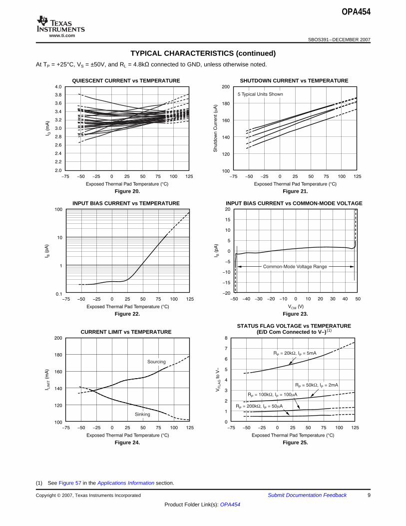
TYPICAL CHARACTERISTICS (continued)At TP = +25°C, VS = ±50V, and RL = 4.8kΩ connected to GND, unless otherwise noted.
QUIESCENT CURRENT vs TEMPERATURE SHUTDOWN CURRENT vs TEMPERATURE
Figure 20. Figure 21.
INPUT BIAS CURRENT vs TEMPERATURE INPUT BIAS CURRENT vs COMMON-MODE VOLTAGE
Figure 22. Figure 23.
STATUS FLAG VOLTAGE vs TEMPERATURECURRENT LIMIT vs TEMPERATURE (E/D Com Connected to V–) (1)
Figure 24. Figure 25.
(1) See Figure 57 in the Applications Information section.
Copyright © 2007, Texas Instruments Incorporated Submit Documentation Feedback 9
Product Folder Link(s): OPA454
www.ti.com
-50 -25 0 25 75 100 125
Exposed Thermal Pad Temperature ( C)°
Dis
sip
ation (
W)
50
2.0
1.5
1.0
0.5
0
T (+125 C max) = T° + [(|V | |V |) I- ´ q ]J OA S O JA
q = +52 C/W, SO-8 PowerPAD°JA
(1in 0.5in´ [25.4mm x 12.7mm]
Heat-Spreader, 1oz Copper)
T = +25 C + (1.93W° ´ 52 C/W) = +125 C° °J
SO-8 PowerPAD:
T = +125 CJ(max) °
-75 0-50 -25 25 125
Exposed Thermal Pad Temperature ( C)°
16
15
14
13
12
11
10
9
8
Sle
w R
ate
(V
/s)
m
50 75 100
G = +1
V = 45VS ±
V = 80V StepIN
R = 4.8kWLOAD
20s/div
5V
/div
m
10 10k100 1k 100k
Frequency (Hz)
1000
100
10
1
Voltage N
ois
e (
nV
/)
ÖH
z
10 10k100 1k 100k
Frequency (Hz)
0.040
0.035
0.030
0.025
0.020
0.015
0.010
TH
D +
N (
%)
G = +10
R = 4.75kWI
V = 38.6VPP
V =S -55, +55
V =S -49, +50
10 10k100 1k 100k
Frequency (Hz)
0.0030
0.0025
0.0020
0.0015
0.0010
0.0005
0
TH
D +
N (
%)
V = +40.6,
39.6S
-
V = +41.6, 40.6-S
G = +1
R = 4.75kI W
V = 38.6VPP
OPA454
SBOS391–DECEMBER 2007
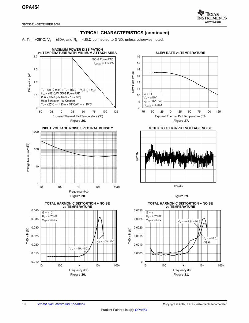
TYPICAL CHARACTERISTICS (continued)At TP = +25°C, VS = ±50V, and RL = 4.8kΩ connected to GND, unless otherwise noted.
MAXIMUM POWER DISSIPATIONvs TEMPERATURE WITH MINIMUM ATTACH AREA SLEW RATE vs TEMPERATURE
Figure 26. Figure 27.
INPUT VOLTAGE NOISE SPECTRAL DENSITY 0.01Hz TO 10Hz INPUT VOLTAGE NOISE
Figure 28. Figure 29.
TOTAL HARMONIC DISTORTION + NOISE TOTAL HARMONIC DISTORTION + NOISEvs TEMPERATURE vs TEMPERATURE
Figure 30. Figure 31.
10 Submit Documentation Feedback Copyright © 2007, Texas Instruments Incorporated
Product Folder Link(s): OPA454

www.ti.com
Time (1ms/div)
50
0m
V/d
iv
VIN
VOUT
G = +1
T = +60 CC °
CLOAD = 50pF
VCM = +30V
RF = 10kW
Time (1ms/div)
50
0m
V/d
iv
VIN
VOUT
G = +1
T = +105 CC °
CLOAD = 50pF
VCM = +30V
RF = 10kW
Time (2.5 s/div)m
V(2
00
mV
/div
)
V(4
00
mV
/div
)IN
OU
T
VIN
VOUT
G = +2
T = +100 CC °
C = 100pFLOAD
V = +40VCM
R = 10kWF
Time (500ns/div)
50
mV
G = +1
C = 100pFLOAD
V = 0VCM
R = 0WF
T = +125 CC °
T = +25 CC °
T = 55- °C C
1ms/div
2.0
1.5
1.0
0.5
0
-0.5
-1.0
-1.5
-2.0
V(V
)O
UT
G = +2
G = +1
R = 10kWF
C = 100pF, 125 C°LOAD
V = +40VCM
0 300100 200 400 500
C (pF)LOAD
180
160
140
120
100
80
60
40
20
0
Peakin
g (
%)
R = 0F W
R = 10kF W
T = +125 C°C
T =C +85 C°
T =C +25 C°
T =C - °55 C
OPA454
SBOS391–DECEMBER 2007
TYPICAL CHARACTERISTICS (continued)At TP = +25°C, VS = ±50V, and RL = 4.8kΩ connected to GND, unless otherwise noted.
LARGE-SIGNAL STEP RESPONSE LARGE-SIGNAL STEP RESPONSE
Figure 32. Figure 33.
LARGE-SIGNAL STEP RESPONSE SMALL-SIGNAL STEP RESPONSE
Figure 34. Figure 35.
GAIN PEAKING vs CLOADSTEP RESPONSE (G = +1, VCM = 0V) (2)
Figure 36. Figure 37.
(2) See Application section Unity-Gain Noninverting Configuration.
Copyright © 2007, Texas Instruments Incorporated Submit Documentation Feedback 11
Product Folder Link(s): OPA454

www.ti.com
0 300100 200 400 500
C (pF)LOAD
30
25
20
15
10
5
0
-5
Peakin
g (
%)
C = 0pFF
C = 2.5pFF
C = 5pFF
T =C +85 C°
T =C +25 C°
T =C - °55 C
T = +125 C°C
10k 100k 1M 10M
Frequency (Hz)
10
8
6
4
2
0
-2
-4
-6
Gain
(dB
)
R = 10k , CWF F = 50pF
R = 0WF
C = 100pFL
C =L 50pF
C = 2L 00pFT = +25 C°A
Time (1 s/div)m
20
15
10
5
0
-5
-10
-15
-20
V(V
)IN
0.08
0.06
0.04
0.02
0
-0.02
-0.04
-0.06
-0.08
Volta
ge a
t Vand V
(V)
12
VIN
V (Noninverting)2
V (Inverting)1
10k 100k 1M 10M
Frequency (Hz)
10
8
6
4
2
0
-2
-4
-6
Gain
(dB
)
C = 0pFF
C = 2.5pFF
C = 5pFF
T = +25 C°A
C = 50pFL
C = 500pFL
OPA454
SBOS391–DECEMBER 2007
TYPICAL CHARACTERISTICS (continued)At TP = +25°C, VS = ±50V, and RL = 4.8kΩ connected to GND, unless otherwise noted.
GAIN PEAKING vs CLOAD(G = +2, RF = 10kΩ, VCM = 0V) GAIN OF +1 vs FREQUENCY (3)
Figure 38. Figure 39.
SETTLING TIME, POSITIVE STEPGAIN OF +2 vs FREQUENCY (4) (20V Step, Gain = 1, RF = 10kΩ) (5) (6)
Figure 40. Figure 41.
(3) See Application section Unity-Gain Noninverting Configuration.(4) See Application section Unity-Gain Noninverting Configuration.(5) See the Settling Time section.(6) The grid for voltage at V1 and V2 is scaled 20mV or 0.1% per division.
12 Submit Documentation Feedback Copyright © 2007, Texas Instruments Incorporated
Product Folder Link(s): OPA454
www.ti.com
Time (1 s/div)m
20
15
10
5
0
-5
-10
-15
-20
V(V
)IN
0.08
0.06
0.04
0.02
0
-0.02
-0.04
-0.06
-0.08
Volta
ge a
t Vand V
(V)
12
VIN
V (Noninverting)2
V (Inverting)1
Time (1 s/div)m
4V
/div
m
OUT
Status Flag
Enable
Time (1 s/div)m
4V
/div
m
OUT
Status Flag
Enable
Time (1 s/div)m
4V
/div
m
OUT
Status Flag
Enable
0 3 41 2 5
V (V)ENABLE
10
0
-10
-20
-30
I(
A)
mE
NA
BLE
-40°C
+25 C°
+85 C°
-75 0-50 -25 25 75 100 125
Temperature ( C)°
1.00
0.95
0.90
0.85
0.80
0.75
0.70
Thre
shold
(V
)
50
OPA454
SBOS391–DECEMBER 2007
TYPICAL CHARACTERISTICS (continued)At TP = +25°C, VS = ±50V, and RL = 4.8kΩ connected to GND, unless otherwise noted.
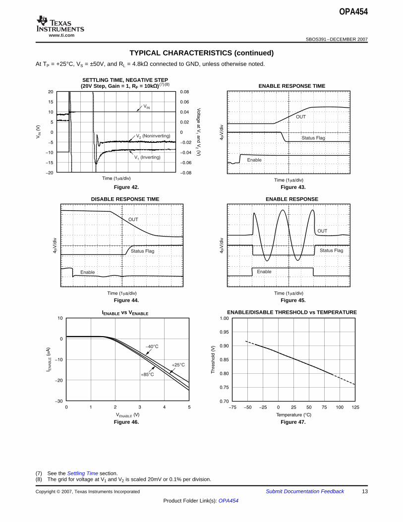
SETTLING TIME, NEGATIVE STEP(20V Step, Gain = 1, RF = 10kΩ) (7) (8) ENABLE RESPONSE TIME
Figure 42. Figure 43.
DISABLE RESPONSE TIME ENABLE RESPONSE
Figure 44. Figure 45.
IENABLE vs VENABLE ENABLE/DISABLE THRESHOLD vs TEMPERATURE
Figure 46. Figure 47.
(7) See the Settling Time section.(8) The grid for voltage at V1 and V2 is scaled 20mV or 0.1% per division.
Copyright © 2007, Texas Instruments Incorporated Submit Documentation Feedback 13
Product Folder Link(s): OPA454
www.ti.com
10 s/divm
60
50
40
30
20
10
0
-10
200
150
100
50
0
-50
-100
-150
V(V
)F
LA
G
I(m
A)
OU
T
VFLAG
IOUT
R = 100kWP
10 s/divm
60
50
40
30
20
10
0
-10
150
100
50
0
-50
-100
-150
-200
V(V
)F
LA
G
I(m
A)
OU
T
VFLAG
IOUT
R = 100kWP
10 s/divm
60
50
40
30
20
10
0
-10
150
100
50
0
-50
-100
-150
-200
V(V
)F
LA
G
I(m
A)
OU
T
VFLAG
IOUT
R = 100kWP
10 s/divm
1.6
1.4
1.2
1.0
0.8
0.6
0.4
0.2
0
-0.2
V(V
)O
UT
+125 C°
+85 C°
+25 C°
- °55 C-50V
+50V
2Hz
2ms Pulse
Mercury
Wetted
Relay
0.988VPP
0.01Hz
+
-
OPA454
10 s/divm
0.2
0
-0.2
-0.4
-0.6
-0.8
-1.0
-1.2
-1.4
-1.6
V(V
)O
UT
+125°C+85°C+25°C
- °55 C
-50V
+50V
2Hz
2ms Pulse
Mercury
Wetted
Relay
0.988VPP
0.01Hz
+
-
OPA454
10 s/divm
0.2
0
-0.2
-0.4
-0.6
-0.8
-1.0
-1.2
-1.4
-1.6
V(V
)O
UT
+125°C+85°C+25°C
- °55 C-50V
+50V
2Hz
2ms Pulse
Mercury
Wetted
Relay
0.988VPP
0.01Hz
+
-
OPA454
OPA454
SBOS391–DECEMBER 2007
TYPICAL CHARACTERISTICS (continued)At TP = +25°C, VS = ±50V, and RL = 4.8kΩ connected to GND, unless otherwise noted.
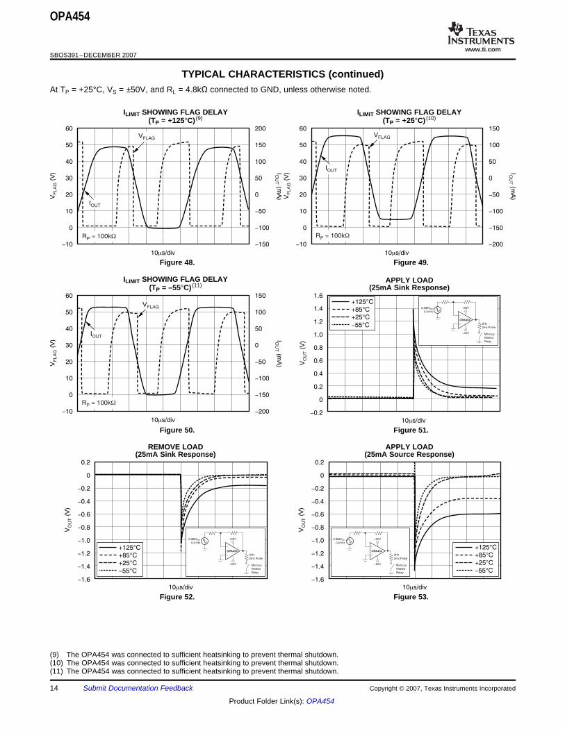
ILIMIT SHOWING FLAG DELAY ILIMIT SHOWING FLAG DELAY(TP = +125°C) (9) (TP = +25°C) (10)
Figure 48. Figure 49.
ILIMIT SHOWING FLAG DELAY APPLY LOAD(TP = –55°C) (11) (25mA Sink Response)
Figure 50. Figure 51.
REMOVE LOAD APPLY LOAD(25mA Sink Response) (25mA Source Response)
Figure 52. Figure 53.
(9) The OPA454 was connected to sufficient heatsinking to prevent thermal shutdown.(10) The OPA454 was connected to sufficient heatsinking to prevent thermal shutdown.(11) The OPA454 was connected to sufficient heatsinking to prevent thermal shutdown.
14 Submit Documentation Feedback Copyright © 2007, Texas Instruments Incorporated
Product Folder Link(s): OPA454
www.ti.com
20ms/div
0
20
V/d
iv
Flag
VOUT
V+RL = 1.8kW
V-
Delay in V is due to-
test equipment.
Power supplies may be
applied in any sequence.
10 s/divm
1.6
1.4
1.2
1.0
0.8
0.6
0.4
0.2
0
-0.2
V(V
)O
UT
+125 C°
+85 C°
+25 C°
- °55 C
-50V
+50V
2Hz
2ms Pulse
Mercury
Wetted
Relay
0.988VPP
0.01Hz
+
-
OPA454
20ms/div
0
20
V/d
iv
Flag
VOUT
V+ RL = 1.8kW
V-
OPA454
SBOS391–DECEMBER 2007
TYPICAL CHARACTERISTICS (continued)At TP = +25°C, VS = ±50V, and RL = 4.8kΩ connected to GND, unless otherwise noted.
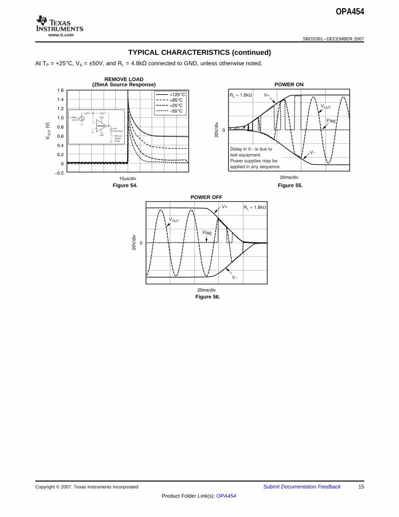
REMOVE LOAD(25mA Source Response) POWER ON
Figure 54. Figure 55.
POWER OFF
Figure 56.
Copyright © 2007, Texas Instruments Incorporated Submit Documentation Feedback 15
Product Folder Link(s): OPA454

www.ti.com
APPLICATIONS INFORMATIONPOWER SUPPLIES
INPUT PROTECTION
RL
R2R1
OPA454
V-
V+
V+
VIN
G = 1+R2
R1
0.1 Fm
0.1 Fm
VOUT
Status
Flag
E/D Com
R(1)
P
IP
VOUT
E/D
V+
V-
V-
-IN
+IN
LOWERING OFFSET VOLTAGE AND DRIFT
R , 1st2
39.1kW
R , 1st1
10kW
OPA735
V+
1st Stage, +5V
V-
1st Stage, 5V-
R , 2nd2
84.5kW
R , 2nd1
10kW
OPA454
V+
2nd Stage, +50V
V-
2nd Stage, 50V-
A , 1st Stage1
A , 2nd Stage2
V 2nd StageOUT
V 1st StageOUT
RLOAD
10kW
Low Offset, 5 V, Drift,m
0.05 V/ C, Self-Zeroing Op Ampm °
Gain 1st = 4.9V/V
High-Voltage Op Amp
Gain 2nd = 9.45V/V
V = 1V±INPUT PP
V 1st Stage 4.9V, MaxOUT ±
V 2nd Stage 46V (92V ), MaxOUT PP±
V = 1VG ±
OPA454
SBOS391–DECEMBER 2007
Figure 57 shows the OPA454 connected as a basicnoninverting amplifier. The OPA454 can be used in The OPA454 may be operated from power suppliesvirtually any ±5V to ±50V op amp configuration. It is up to ±50V or a total of 100V with excellentespecially useful for supply voltages greater than performance. Most behavior remains unchanged36V. throughout the full operating voltage range.
Parameters that vary significantly with operatingPower-supply terminals should be bypassed with voltage are shown in the Typical Characteristics.0.1µF (or greater) capacitors, located near thepower-supply pins. Be sure that the capacitors are Some applications do not require equal positive andappropriately rated for the power-supply voltage negative output voltage swing. Power-supply voltagesused. do not need to be equal. The OPA454 can operate
with as little as 10V between the supplies and with upto 100V between the supplies. For example, thepositive supply could be set to 90V with the negativesupply at –10V, or vice-versa (as long as the total isless than or equal to 100V).
The OPA454 has increased protection againstdamage caused by excessive voltage between opamp input pins or input pin voltages that exceed thepower supplies; external series resistance is notneeded for protection. Internal series JFETs limitinput overload current to a non-destructive 4mA, evenwith an input differential voltage as large as 120V.Additionally, the OPA454 has dielectric isolationbetween devices and the substrate. Therefore, theamplifier is free from the limitations of junction
(1) Pull-up resistor with at least 10µA (choose isolation common to many IC fabrication processes.RP = 1MΩ with V+ = 50V for IP = 50µA).
Figure 57. Basic Noninverting AmplifierConfiguration The OPA454 can be used with an OPA735 zero-drift
series op amp to create a high-voltage op amp circuitthat has very low input offset temperature drift. Thiscircuit is shown in Figure 58.
Figure 58. Two-Stage, High-Voltage Op Amp Circuit With Very Low Input Offset Temperature Drift
16 Submit Documentation Feedback Copyright © 2007, Texas Instruments Incorporated
Product Folder Link(s): OPA454
www.ti.com
INCREASING OUTPUT CURRENT R1 R2
OPA454
OPA454
SLAVE
MASTER
VIN
R(1)
10W
S
R(1)
10W
S
RL
A1
A2
UNITY-GAIN NONINVERTING
R1 R2
OPA454
PNP
TIP30C, MJL21193,
MJE15004, MJL1302A
NPN
TIP29C, MJL21194,
MJE15003, MJL3281
VIN
+50V
-50V
V(3)
O OUT L L= V I R-
R(1)
20W
3
R
0.2W
5
R
0.2W
4
RL
CF
-IN
+IN
V+
V-
VOUT
(2)
IL
OPA454
SBOS391–DECEMBER 2007
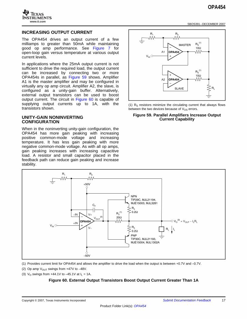
The OPA454 drives an output current of a fewmilliamps to greater than 50mA while maintaininggood op amp performance. See Figure 7 foropen-loop gain versus temperature at various outputcurrent levels.
In applications where the 25mA output current is notsufficient to drive the required load, the output currentcan be increased by connecting two or moreOPA454s in parallel, as Figure 59 shows. AmplifierA1 is the master amplifier and may be configured invirtually any op amp circuit. Amplifier A2, the slave, isconfigured as a unity-gain buffer. Alternatively,external output transistors can be used to boostoutput current. The circuit in Figure 60 is capable ofsupplying output currents up to 1A, with the (1) RS resistors minimize the circulating current that always flowstransistors shown. between the two devices because of VOS errors.
Figure 59. Parallel Amplifiers Increase OutputCurrent CapabilityCONFIGURATION
When in the noninverting unity-gain configuration, theOPA454 has more gain peaking with increasingpositive common-mode voltage and increasingtemperature. It has less gain peaking with morenegative common-mode voltage. As with all op amps,gain peaking increases with increasing capacitiveload. A resistor and small capacitor placed in thefeedback path can reduce gain peaking and increasestability.
(1) Provides current limit for OPA454 and allows the amplifier to drive the load when the output is between +0.7V and –0.7V.(2) Op amp VOUT swings from +47V to –48V.(3) VO swings from +44.1V to –45.1V at IL = 1A.
Figure 60. External Output Transistors Boost Output Current Greater Than 1A
Copyright © 2007, Texas Instruments Incorporated Submit Documentation Feedback 17
Product Folder Link(s): OPA454

www.ti.com
INPUT RANGE
0 6020 40 100
Time ( s)m
-46.0
-46.5
-47.0
-47.5
-48.0
-48.5
-50.5
Voltage (
V)
80
-49.0
V-
V
f = 1kHzIN
V
R = 50kOUT
S W
T = +25 C°A
V
R = 0OUT
S W
-49.5
-50.0
0 6020 40 100
Time ( s)m
50.5
50.0
49.5
49.0
48.5
48.0
47.0
Voltage (
V)
80
47.5
V+
V
f = 1kHzIN V
R = 50kOUT
S W
T = +25 C°A
V
R = 0OUT
S W
R
10kW
F
R
4.8kW
L
RS OPA454
V+ = +50V
V = 50V- -VIN
VOUT
OUTPUT RANGE
0 6020 40 100
Time ( s)m
-46.0
-46.5
-47.0
-47.5
-48.0
-48.5
-50.5
Voltage (
V)
80
-49.0
V-
V
f = 1kHzIN
V
R = 50kOUT
S W
T = +25 C°A
V
R = 0OUT
S W
-49.5
-50.0
OPA454
SBOS391–DECEMBER 2007
The OPA454 is specified to give linear operation withinput swing to within 2.5V of either supply. Generally,a gain of +1 is the most demanding configuration.Figure 61 and Figure 62 show output behavior as theinput swings to within 0V of the rail, using the circuitshown in Figure 64. Figure 63 shows the behaviorwith an input signal that swings beyond the specifiedinput range to within 1V of the rail, also using thecircuit in Figure 64. Notice that the beginning of thephase reversal effect may be reduced by insertingseries resistance (RS) in the connection to thepositive input. Note that VOUT does not swing all theway to the opposite rail.
Figure 63. Output Voltage With Input VoltageDown To (V–) + 1V
Figure 61. Output Voltage With Input Voltage Up Figure 64. Input Range Test CircuitTo V+
The OPA454 is specified to swing to within 1V ofeither supply rail with a 49kΩ load while maintainingexcellent linearity. Swing to the rail decreases withincreasing output current. The OPA454 can swing towithin 2V of the negative rail and 3V of the positiverail with a 1.88kΩ load. The typical characteristiccurve, Output Voltage Swing vs Output Current(Figure 11), shows this behavior in detail.
Figure 62. Output Voltage With Input VoltageDown To V–
18 Submit Documentation Feedback Copyright © 2007, Texas Instruments Incorporated
Product Folder Link(s): OPA454
www.ti.com
OPEN-LOOP GAIN LINEARITY SETTLING TIME
-50 0-40 -30 -20 -10 10 30 40 50
Output Voltage (V)
|(V
)(V
-)|
IN+
IN-
20
A is a Function of V and IOL OUT LOAD
T = +25 CP °
RL = 1880W, 1mV/div
89dB
106dB
74dBRL = 900W, 2mV/div
R = 4.87kW mL , 200 V/div
R7 R8
R
10kW
5 R
10kW
6
R3
R
10kW
4
R1
R
10kW
2
Inverting Response
Measured Here, V1
Combination of Both
Inverting and
Noninverting Responses, V2
VIN
-IN
+IN
VOUTOPA454 OPA454
VOUT
-IN
+INA1 A2
OPA454
SBOS391–DECEMBER 2007
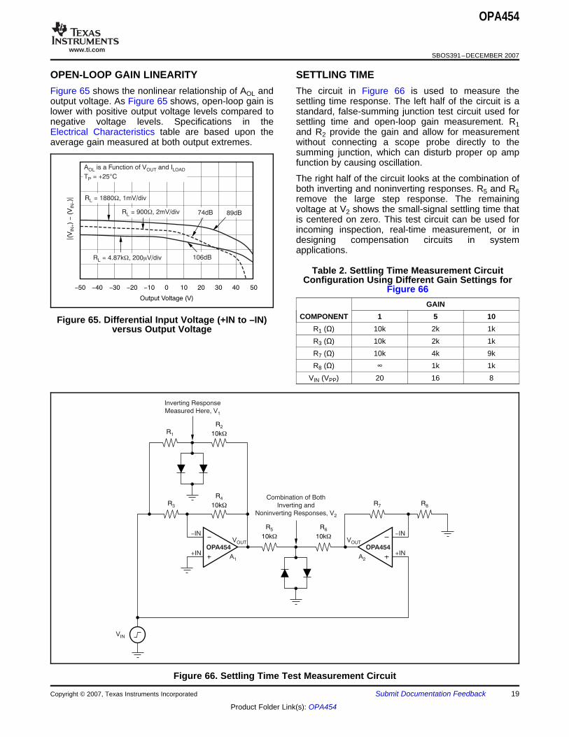
Figure 65 shows the nonlinear relationship of AOL and The circuit in Figure 66 is used to measure theoutput voltage. As Figure 65 shows, open-loop gain is settling time response. The left half of the circuit is alower with positive output voltage levels compared to standard, false-summing junction test circuit used fornegative voltage levels. Specifications in the settling time and open-loop gain measurement. R1Electrical Characteristics table are based upon the and R2 provide the gain and allow for measurementaverage gain measured at both output extremes. without connecting a scope probe directly to the
summing junction, which can disturb proper op ampfunction by causing oscillation.
The right half of the circuit looks at the combination ofboth inverting and noninverting responses. R5 and R6remove the large step response. The remainingvoltage at V2 shows the small-signal settling time thatis centered on zero. This test circuit can be used forincoming inspection, real-time measurement, or indesigning compensation circuits in systemapplications.
Table 2. Settling Time Measurement CircuitConfiguration Using Different Gain Settings for
Figure 66GAIN
COMPONENT 1 5 10Figure 65. Differential Input Voltage (+IN to –IN)R1 (Ω) 10k 2k 1kversus Output VoltageR3 (Ω) 10k 2k 1kR7 (Ω) 10k 4k 9kR8 (Ω) ∞ 1k 1k
VIN (VPP) 20 16 8
Figure 66. Settling Time Test Measurement Circuit
Copyright © 2007, Texas Instruments Incorporated Submit Documentation Feedback 19
Product Folder Link(s): OPA454

www.ti.com
ENABLE AND E/D Com
THERMAL PROTECTION
OPA454
-IN
+IN
V-
V+
E/D Com
E/D
VOUT
DVDD
(Digital Supply)
5V Logic
RP
V+
(Positive Op Amp Supply)
V
(Negative Op Amp Supply)
-
IP
CURRENT LIMIT
0 800200 400 1000
(ms)
40
20
0
-120
V(V
)O
UT
-20
-40
-60
-80
-100
140
120
100
-20
V(V
)F
LA
G
80
60
40
20
0
600
VOUT
VFLAG
100kW10kW
E/D Com
-50V
+50V
VFLAGFlag
VOUT
RP
1MW
625W
+2.5V
10Hz Square Wave
VOUT
V+-IN
+IN
V-
OPA454
OPA454
SBOS391–DECEMBER 2007
avoided to maximize reliability. It is always best toprovide proper heat-sinking (either by a physical plateor by airflow) to remain considerably below the
If left disconnected, E/D Com is pulled near V– thermal shutdown threshold. For longest operational(negative supply) by an internal 10µA current source. life of the device, keep the junction temperatureWhen left floating, ENABLE is held approximately 2V below +125°C.above E/D Com by an internal 1µA source. Eventhough active operation of the OPA454 results whenthe ENABLE and E/D Com pins are not connected, amoderately fast, negative-going signal capacitively Figure 68 shows the thermal shutdown behavior of acoupled to the ENABLE pin can overpower the 1µA socketed OPA454 that internally dissipates 1W.pull-up current and cause device shutdown. This Unsoldered and in a socket, θJA of the DDA packagebehavior can appear as an oscillation and is is typically +128°C/W. With the socket at +25°C, theencountered first near extreme cold temperatures. If output stage temperature rises to the shutdownthe enable function is not used, a conservative temperature of +150°C, which triggers automaticapproach is to connect ENABLE through a 30pF thermal shutdown of the device. The device remainscapacitor to a low impedance source. Another in thermal shutdown (output is in a high-impedancealternative is the connection of an external current state) until it cools to +130°C where it again issource from V+ (positive supply) sufficient to hold the powered. This thermal protection hysteresis featureenable level above the shutdown threshold. Figure 67 typically prevents the amplifier from leaving the safeshows a circuit that connects ENABLE and E/D Com. operating area, even with a direct short from theChoosing RP to be 1MΩ with a +50V positive power output to ground or either supply. The rail-to-railsupply voltage results in IP = 50µA. supply voltage at which catastrophic breakdown
occurs is typically 135V at +25°C. However, theabsolute maximum specification is 120V, and theOPA454 should not be allowed to exceed 120V underany condition. Failure as a result of breakdown,caused by spiking currents into inductive loads(particularly with elevated supply voltage), is notprevented by the thermal protection architecture.
Figure 67. ENABLE and E/D Com
Figure 24 and Figure 48 to Figure 50 show thecurrent limit behavior of the OPA454. Current limitingis accomplished by internally limiting the drive to theoutput transistors. The output can supply the limitedcurrent continuously, unless the die temperature risesto +150°C, which initiates thermal shutdown. Withadequate heat-sinking, and use of the lowest possiblesupply voltage, the OPA454 can remain in currentlimit continuously without entering thermal shutdown.Although qualification studies have shown minimalparametric shifts induced by 400 hours of thermalshutdown cycling, this mode of operation should be Figure 68. Thermal Shutdown
20 Submit Documentation Feedback Copyright © 2007, Texas Instruments Incorporated
Product Folder Link(s): OPA454
www.ti.com
POWER DISSIPATION HEATSINKING
T = T + P qJ A D JA (1)
0 0.5 1.0 1.5 2.0 2.5 3.0
Copper Area (inches ), 2 oz2
Therm
al R
esis
tance,
q°
JA
(C
/W)
60
50
40
30
20
10
0
OPA454
R
100kW
1
Compliance Voltage Range = +47V, 48V-
+50V
R
10kW
2
R3
100kW
R
9.9kW
4
-50V
R
100W
5
IL RL
I = [(V - V )/R ] (R /R )
= (V V )/1k- W
L 5 2 1
2 1
2 1
V2
V1
-IN
+IN
V-
V+VOUT
OPA454
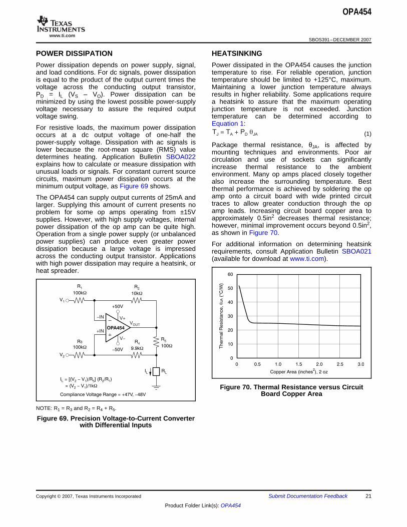
SBOS391–DECEMBER 2007
Power dissipation depends on power supply, signal, Power dissipated in the OPA454 causes the junctionand load conditions. For dc signals, power dissipation temperature to rise. For reliable operation, junctionis equal to the product of the output current times the temperature should be limited to +125°C, maximum.voltage across the conducting output transistor, Maintaining a lower junction temperature alwaysPD = IL (VS – VO). Power dissipation can be results in higher reliability. Some applications requireminimized by using the lowest possible power-supply a heatsink to assure that the maximum operatingvoltage necessary to assure the required output junction temperature is not exceeded. Junctionvoltage swing. temperature can be determined according to
Equation 1:For resistive loads, the maximum power dissipationoccurs at a dc output voltage of one-half thepower-supply voltage. Dissipation with ac signals is Package thermal resistance, θJA, is affected bylower because the root-mean square (RMS) value mounting techniques and environments. Poor airdetermines heating. Application Bulletin SBOA022 circulation and use of sockets can significantlyexplains how to calculate or measure dissipation with increase thermal resistance to the ambientunusual loads or signals. For constant current source environment. Many op amps placed closely togethercircuits, maximum power dissipation occurs at the also increase the surrounding temperature. Bestminimum output voltage, as Figure 69 shows. thermal performance is achieved by soldering the op
amp onto a circuit board with wide printed circuitThe OPA454 can supply output currents of 25mA andtraces to allow greater conduction through the oplarger. Supplying this amount of current presents noamp leads. Increasing circuit board copper area toproblem for some op amps operating from ±15Vapproximately 0.5in2 decreases thermal resistance;supplies. However, with high supply voltages, internalhowever, minimal improvement occurs beyond 0.5in2,power dissipation of the op amp can be quite high.as shown in Figure 70.Operation from a single power supply (or unbalanced
power supplies) can produce even greater power For additional information on determining heatsinkdissipation because a large voltage is impressed requirements, consult Application Bulletin SBOA021across the conducting output transistor. Applications (available for download at www.ti.com).with high power dissipation may require a heatsink, orheat spreader.
Figure 70. Thermal Resistance versus CircuitBoard Copper Area
NOTE: R1 = R3 and R2 = R4 + R5.
Figure 69. Precision Voltage-to-Current Converterwith Differential Inputs
Copyright © 2007, Texas Instruments Incorporated Submit Documentation Feedback 21
Product Folder Link(s): OPA454
www.ti.com
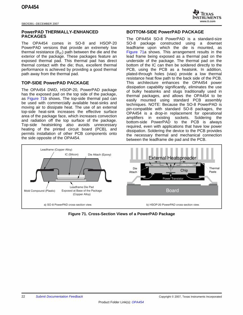
PowerPAD THERMALLY-ENHANCED BOTTOM-SIDE PowerPAD PACKAGE
TOP-SIDE PowerPAD PACKAGE
Mold Compound (Plastic)
Leadframe Die Pad
Exposed at Base of the Package
(Copper Alloy)
Leadframe (Copper Alloy)
IC (Silicon) Die Attach (Epoxy)
a) SO-8 PowerPAD cross-section view. b) HSOP-20 PowerPAD cross-section view.
Board
External Heatspreader
Power Transistor
Chip
Die Pad
Die
Attach
Thermal
Paste
OPA454
SBOS391–DECEMBER 2007
PACKAGES The OPA454 SO-8 PowerPAD is a standard-sizeThe OPA454 comes in SO-8 and HSOP-20 SO-8 package constructed using a downsetPowerPAD versions that provide an extremely low leadframe upon which the die is mounted, asthermal resistance (θJC) path between the die and the Figure 71a shows. This arrangement results in theexterior of the package. These packages feature an lead frame being exposed as a thermal pad on theexposed thermal pad. This thermal pad has direct underside of the package. The thermal pad on thethermal contact with the die; thus, excellent thermal bottom of the IC can then be soldered directly to theperformance is achieved by providing a good thermal PCB, using the PCB as a heatsink. In addition,path away from the thermal pad. plated-through holes (vias) provide a low thermal
resistance heat flow path to the back side of the PCB.This architecture enhances the OPA454 powerdissipation capability significantly, eliminates the use
The OPA454 DWD, HSOP-20, PowerPAD package of bulky heatsinks and slugs traditionally used inhas the exposed pad on the top side of the package, thermal packages, and allows the OPA454 to beas Figure 71b shows. The top-side thermal pad can easily mounted using standard PCB assemblybe used with commercially available heat-sinks and techniques. NOTE: Because the SO-8 PowerPAD ismoving air to dissipate heat. The use of an external pin-compatible with standard SO-8 packages, thetop-side heat-sink increases the effective surface OPA454 is a drop-in replacement for operationalarea of the package face, which increases convection amplifiers in existing sockets. Soldering theand radiation off the top surface of the package. bottom-side PowerPAD to the PCB is alwaysTop-side heatsinking also avoids unnecessary required, even with applications that have low powerheating of the printed circuit board (PCB), and dissipation. Soldering the device to the PCB providespermits installation of other PCB components onto the necessary thermal and mechanical connectionthe side opposite of the OPA454. between the leadframe die pad and the PCB.
Figure 71. Cross-Section Views of a PowerPAD Package
22 Submit Documentation Feedback Copyright © 2007, Texas Instruments Incorporated
Product Folder Link(s): OPA454

www.ti.com
BOTTOM-SIDE PowerPAD LAYOUT
OPA454
SBOS391–DECEMBER 2007
area to be soldered; thus, wicking is not aGUIDELINES problem.
6. Connect all holes to the internal power plane ofThe PowerPAD package allows for both assemblythe correct voltage potential (V–).and thermal management in one manufacturing
operation. During the surface-mount solder operation 7. When connecting these holes to the plane, do not(when the leads are being soldered), the thermal pad use the typical web or spoke via connectionmust be soldered to a copper area underneath the methodology. Web connections have a highpackage. Through the use of thermal paths within this thermal resistance connection that is useful forcopper area, heat can be conducted away from the slowing the heat transfer during solderingpackage into either a ground plane or other operations, making the soldering of vias that haveheat-dissipating device. Soldering the PowerPAD to plane connections easier. In this application,the PCB is always required, even with applications however, low thermal resistance is desired for thethat have low power dissipation. Follow these steps most efficient heat transfer. Therefore, the holesto attach the device to the PCB: under the OPA454 PowerPAD package should
make the connections to the internal plane with a1. The PowerPAD must be connected to the mostcomplete connection around the entirenegative supply voltage on the device, V–.circumference of the plated-through hole.2. Prepare the PCB with a top-side etch pattern.
8. The top-side solder mask should leave theThere should be etching for the leads as well asterminals of the package and the thermal padetch for the thermal pad.area exposed. The bottom-side solder mask3. Use of thermal vias improves heat dissipation, should cover the holes of the thermal pad area.but are not required. The thermal pad can This masking prevents solder from being pulledconnect to the PCB using an area equal to the away from the thermal pad area during the reflowpad size with no vias, but externally connected to process.V–.
9. Apply solder paste to the exposed thermal pad4. Place recommended holes in the area of the area and all of the IC terminals.thermal pad. Recommended thermal land size10. With these preparatory steps in place, theand thermal via patterns for the SO-8 DDA
PowerPAD IC is simply placed in position and runpackage are shown in the thermal land patternthrough the solder reflow operation as anymechanical drawing appended at the end of thisstandard surface-mount component. Thisdocument. These holes should be 13 mils inpreparation results in a properly installed part.diameter. Keep them small, so that solder wicking
through the holes is not a problem during reflow. For detailed information on the PowerPAD package,The minimum recommended number of holes for including thermal modeling considerations and repairthe SO-8 PowerPAD package is five. procedures, see technical brief SLMA002 PowerPAD
5. Additional vias may be placed anywhere along Thermally-Enhanced Package, available for downloadthe thermal plane outside of the thermal pad at www.ti.com.area. These vias help dissipate the heatgenerated by the OPA454 IC. These additionalvias may be larger than the 13-mil diameter viasdirectly under the thermal pad. They can belarger because they are not in the thermal pad
Copyright © 2007, Texas Instruments Incorporated Submit Documentation Feedback 23
Product Folder Link(s): OPA454
www.ti.com
TYPICAL APPLICATIONS
OPA454
0-2mA
+95V
45.3kW
-5V
V = 0V to +91VOUT
0.1 Fm
0.1 Fm
Protects DAC
During Slewing
DAC8811
or
DAC7811
-IN
+IN
V-
V+
RL
+50V
Up To
195V
Piezo(1)
Crystal
-50V
MASTER
R
9kW
2R
1kW
1
V
±4VIN
OPA454
+50V
-50V
SLAVE
R
10kW
4
R
10kW
3
OPA454
-IN
+IN
-IN
+IN
VOUT VOUT
V+ V+
V- V-
A1 A2
OPA454
SBOS391–DECEMBER 2007
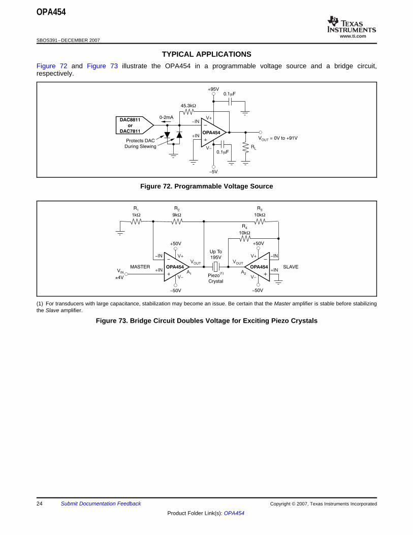
Figure 72 and Figure 73 illustrate the OPA454 in a programmable voltage source and a bridge circuit,respectively.
Figure 72. Programmable Voltage Source
(1) For transducers with large capacitance, stabilization may become an issue. Be certain that the Master amplifier is stable before stabilizingthe Slave amplifier.
Figure 73. Bridge Circuit Doubles Voltage for Exciting Piezo Crystals
24 Submit Documentation Feedback Copyright © 2007, Texas Instruments Incorporated
Product Folder Link(s): OPA454
www.ti.com
R2
R1
VSIG
OPA454
V+
V-
R4 R5
R2
OPA454
V-
V+R6 R7
OPA454
V+
V-
VOUT
VOUT 2 1 2 1= (1 + 2R /R ) (V V )-
V1
V2
VCM
A1
A2
A3
(1)
R2
R1
OPA454
V+
V-
R4 R5
RSHUNT
R2
OPA454
V-
V+R6 R7
OPA454
V+
V-
VOUT
VSUPPLY
Plus
Minus
orLoad
V = (1 + 2R /ROUT 2 1 2 1) (V V )-
V1
V2
A1
(1)
A2
(1)
A3
(2)
OPA454
SBOS391–DECEMBER 2007
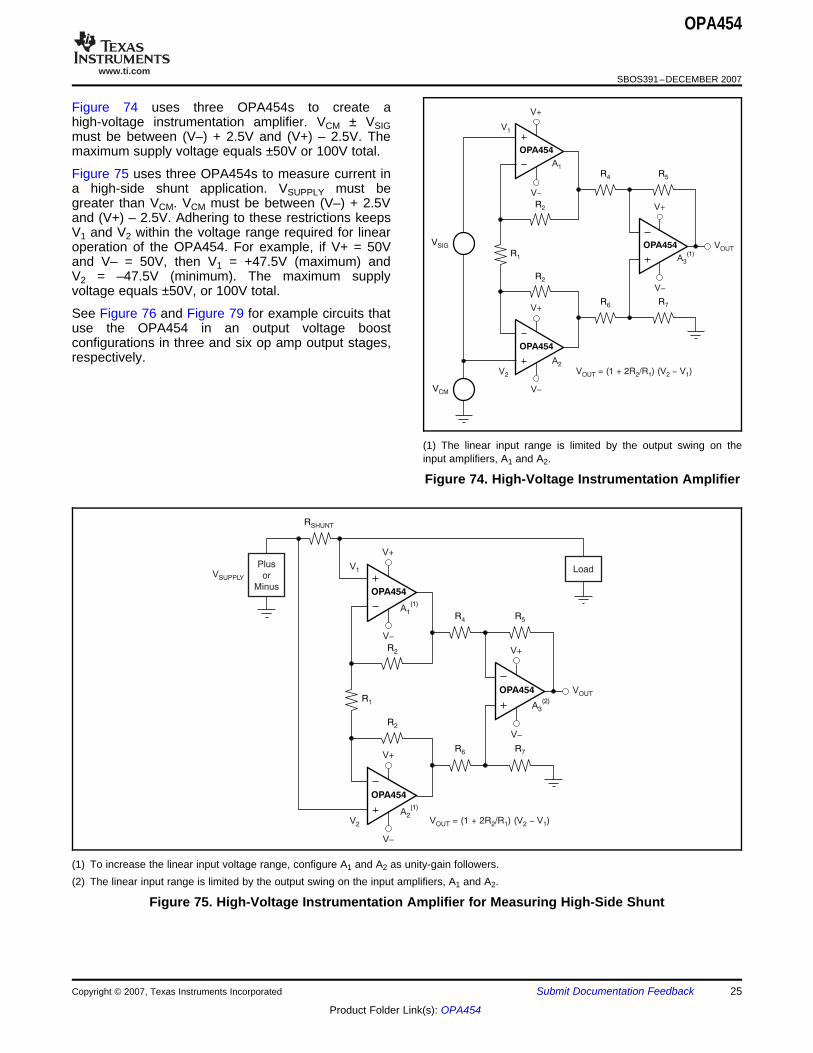
Figure 74 uses three OPA454s to create ahigh-voltage instrumentation amplifier. VCM ± VSIGmust be between (V–) + 2.5V and (V+) – 2.5V. Themaximum supply voltage equals ±50V or 100V total.
Figure 75 uses three OPA454s to measure current ina high-side shunt application. VSUPPLY must begreater than VCM. VCM must be between (V–) + 2.5Vand (V+) – 2.5V. Adhering to these restrictions keepsV1 and V2 within the voltage range required for linearoperation of the OPA454. For example, if V+ = 50Vand V– = 50V, then V1 = +47.5V (maximum) andV2 = –47.5V (minimum). The maximum supplyvoltage equals ±50V, or 100V total.
See Figure 76 and Figure 79 for example circuits thatuse the OPA454 in an output voltage boostconfigurations in three and six op amp output stages,respectively.
(1) The linear input range is limited by the output swing on theinput amplifiers, A1 and A2.
Figure 74. High-Voltage Instrumentation Amplifier
(1) To increase the linear input voltage range, configure A1 and A2 as unity-gain followers.(2) The linear input range is limited by the output swing on the input amplifiers, A1 and A2.
Figure 75. High-Voltage Instrumentation Amplifier for Measuring High-Side Shunt
Copyright © 2007, Texas Instruments Incorporated Submit Documentation Feedback 25
Product Folder Link(s): OPA454

www.ti.com
10kW
OPA454
+100V
+100V
10kW
OPA454
190kW
V+
V-
10kW
OPA454
-100V
-100V
100kW
RLOAD
3.75kW
100kW
100kW
100kW
a) Noninverting, G = +20V/V
10kW
OPA454
+100V
+100V
10kW
OPA454
200kW
V+
V-
10kW
OPA454
-100V
-100V
100kW
R
3.75kLOAD
W
100kW
100kW
100kW
b) Inverting, G = 20V/V-
VOUT
V+
V-
V = +97V, 98V
(195V )
-LOAD
PP
V = +97V, 98V
(195V )
-LOAD
PP
V+
V-
VOUT
V01
V02
V04
V05
V+
V-
V+
V-
A1
A2
A3
A4
A5
A6
VIN
VIN
Time (10 s/div)m
100
80
60
0
-20
-40
-100
V(V
)O
UT
6
4
2
0
-2
-4
-6
V(V
)IN
VIN
VOUT
40
20
-60
-80
Time (20 s/div)m
0
Voltage (
V)
V01
V02
VLOAD
100
-100
75
25
50
-75
-25
-50
OPA454
SBOS391–DECEMBER 2007
Figure 76. Output Voltage Boost With +97V, –98V (195VPP) Across Load Connected to Ground (3 Op AmpOutput Stage, see Figure 77 and Figure 78)
Figure 78. 3.75kΩ Load to GroundFigure 77. 195VPP On 3.75kΩ Load to GroundG = +20, 3 OPA454s, 100V Supplies20kHz, Uses 3 OPA454s, 100V Supplies
(Note SR of 18V/µs, which is slightly higher thanthe specified 13V/µs due to tracking of the
power-supply voltage)
26 Submit Documentation Feedback Copyright © 2007, Texas Instruments Incorporated
Product Folder Link(s): OPA454
www.ti.com
RLOAD
7.5kW
10kW
OPA454A1
+120V
+100V
10kW
OPA454A2
190kW10kW
OPA454A3
-100V
-100V
10kW
OPA454A4
+120V
10kW
OPA454A5
200kW 10kW
OPA454A6
-100V
100kW
100kW
100kW
100kW
-100V
100kW
100kW
+100V
100kW
100kW
(+97V, 98V)- ( +97V)-98V,
VIN
VLOAD
PP( 195V, 390V )±
V+
V+
V+
V-
V-
V- V-
V+
V-
V-
V+
V+
Time (10 s/div)m
200
150
100
50
0
-50
-100
-150
-200
V(V
)O
UT
6
4
2
0
-2
-4
-6
V(V
)IN
VINVOUT
Time (20 s/div)m
0
V(V
)O
UT
VLOAD
200
-200
150
100
50
-50
-100
-150
OPA454
SBOS391–DECEMBER 2007
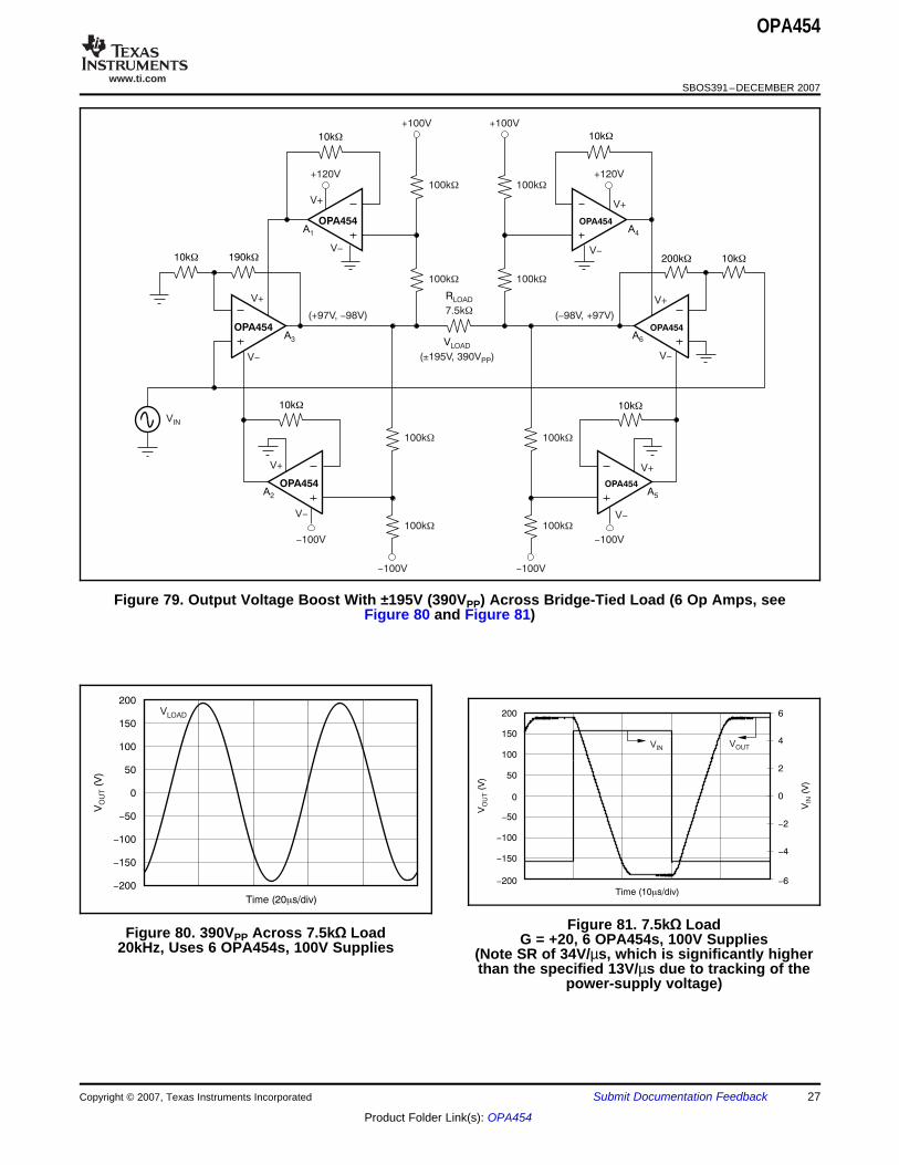
Figure 79. Output Voltage Boost With ±195V (390VPP) Across Bridge-Tied Load (6 Op Amps, seeFigure 80 and Figure 81)
Figure 81. 7.5kΩ LoadFigure 80. 390VPP Across 7.5kΩ Load G = +20, 6 OPA454s, 100V Supplies20kHz, Uses 6 OPA454s, 100V Supplies (Note SR of 34V/µs, which is significantly higherthan the specified 13V/µs due to tracking of the
power-supply voltage)
Copyright © 2007, Texas Instruments Incorporated Submit Documentation Feedback 27
Product Folder Link(s): OPA454
www.ti.com
V = V - VOUT 2 1
V1
V2
R
25kW
3 R
25kW
4
R
25kW
2R
25kW
1
OPA454
HIGH-COMPLIANCE VOLTAGE CURRENT
5ms/div
14
12
10
8
6
4
2
0
-2
V(1
V/d
iv)
OU
T
V(V
)LE
D
0V
-2V
6V
VOUT
VLED
OPA454
V1
V2
Load IO
I = (V -O 2 1V )/R
R
OPA454
25kW 25kW
25kW 25kW
A1
A2
OPA454
SBOS391–DECEMBER 2007
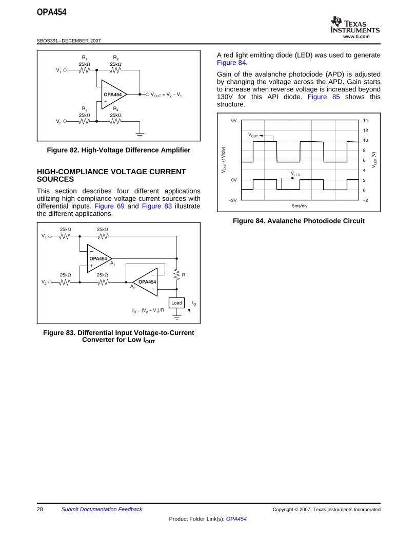
A red light emitting diode (LED) was used to generateFigure 84.
Gain of the avalanche photodiode (APD) is adjustedby changing the voltage across the APD. Gain startsto increase when reverse voltage is increased beyond130V for this API diode. Figure 85 shows thisstructure.
Figure 82. High-Voltage Difference Amplifier
SOURCESThis section describes four different applicationsutilizing high compliance voltage current sources withdifferential inputs. Figure 69 and Figure 83 illustratethe different applications.
Figure 84. Avalanche Photodiode Circuit
Figure 83. Differential Input Voltage-to-CurrentConverter for Low IOUT
28 Submit Documentation Feedback Copyright © 2007, Texas Instruments Incorporated
Product Folder Link(s): OPA454

www.ti.com
R
1kW
2 R
100kW
4
OPA454
+
R
1kW
3
OPA454
OPA454
+100V
OPA454 +100V
APD
R5
100kW
LM4041D
Adjusted for 2.0V
R9
4.9kW
R8
198kW
RSENSE
100WV1
100W
R10
3.1kW
VOUT
V = 100 R´OUT SENSE DI´
R
10kW
7 R
90kW
1
Gain Adjust Voltage
2.5V to 9.5V
-200V
Advanced Photonix, Inc.
SD 036-70-62-531
Digi-Key
SD 036-70-62-531
VLEDLED
V+
V-
A1
+100V
V+
V-
A2
+100V
V+
V-
A3
+100V
V+
V-
A4
Example Circuit For Reverse Biasing APD
(130V to 280V, max)
OPA454
SBOS391–DECEMBER 2007
Figure 85. APD Gain Adjustment Using the OPA454, High-Voltage Op Amp
Copyright © 2007, Texas Instruments Incorporated Submit Documentation Feedback 29
Product Folder Link(s): OPA454
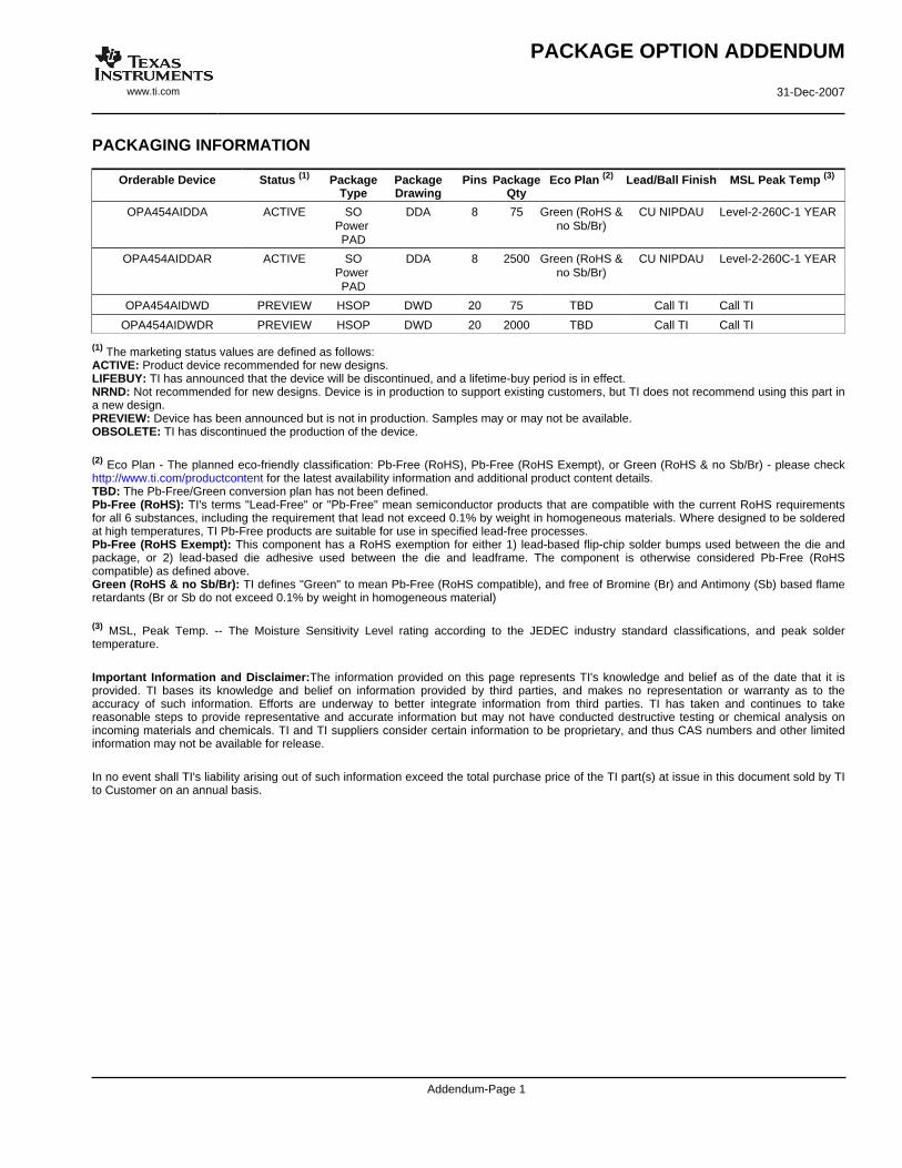
PACKAGING INFORMATION
Orderable Device Status (1) PackageType
PackageDrawing
Pins PackageQty
Eco Plan (2) Lead/Ball Finish MSL Peak Temp (3)
OPA454AIDDA ACTIVE SOPower PAD
DDA 8 75 Green (RoHS &no Sb/Br)
CU NIPDAU Level-2-260C-1 YEAR
OPA454AIDDAR ACTIVE SOPower PAD
DDA 8 2500 Green (RoHS &no Sb/Br)
CU NIPDAU Level-2-260C-1 YEAR
OPA454AIDWD PREVIEW HSOP DWD 20 75 TBD Call TI Call TI
OPA454AIDWDR PREVIEW HSOP DWD 20 2000 TBD Call TI Call TI
(1) The marketing status values are defined as follows:ACTIVE: Product device recommended for new designs.LIFEBUY: TI has announced that the device will be discontinued, and a lifetime-buy period is in effect.NRND: Not recommended for new designs. Device is in production to support existing customers, but TI does not recommend using this part ina new design.PREVIEW: Device has been announced but is not in production. Samples may or may not be available.OBSOLETE: TI has discontinued the production of the device.
(2) Eco Plan - The planned eco-friendly classification: Pb-Free (RoHS), Pb-Free (RoHS Exempt), or Green (RoHS & no Sb/Br) - please checkhttp://www.ti.com/productcontent for the latest availability information and additional product content details.TBD: The Pb-Free/Green conversion plan has not been defined.Pb-Free (RoHS): TI's terms "Lead-Free" or "Pb-Free" mean semiconductor products that are compatible with the current RoHS requirementsfor all 6 substances, including the requirement that lead not exceed 0.1% by weight in homogeneous materials. Where designed to be solderedat high temperatures, TI Pb-Free products are suitable for use in specified lead-free processes.Pb-Free (RoHS Exempt): This component has a RoHS exemption for either 1) lead-based flip-chip solder bumps used between the die andpackage, or 2) lead-based die adhesive used between the die and leadframe. The component is otherwise considered Pb-Free (RoHScompatible) as defined above.Green (RoHS & no Sb/Br): TI defines "Green" to mean Pb-Free (RoHS compatible), and free of Bromine (Br) and Antimony (Sb) based flameretardants (Br or Sb do not exceed 0.1% by weight in homogeneous material)
(3) MSL, Peak Temp. -- The Moisture Sensitivity Level rating according to the JEDEC industry standard classifications, and peak soldertemperature.
Important Information and Disclaimer:The information provided on this page represents TI's knowledge and belief as of the date that it isprovided. TI bases its knowledge and belief on information provided by third parties, and makes no representation or warranty as to theaccuracy of such information. Efforts are underway to better integrate information from third parties. TI has taken and continues to takereasonable steps to provide representative and accurate information but may not have conducted destructive testing or chemical analysis onincoming materials and chemicals. TI and TI suppliers consider certain information to be proprietary, and thus CAS numbers and other limitedinformation may not be available for release.
In no event shall TI's liability arising out of such information exceed the total purchase price of the TI part(s) at issue in this document sold by TIto Customer on an annual basis.
PACKAGE OPTION ADDENDUM
www.ti.com 31-Dec-2007
Addendum-Page 1
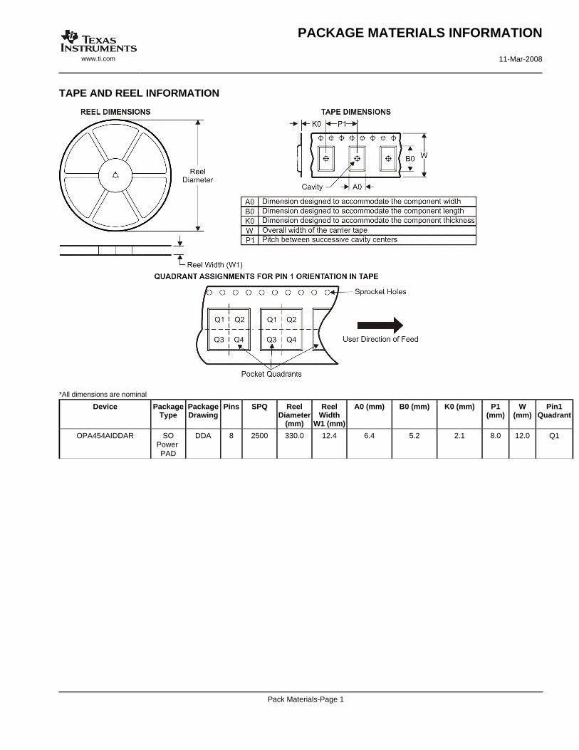
TAPE AND REEL INFORMATION
*All dimensions are nominal
Device PackageType
PackageDrawing
Pins SPQ ReelDiameter
(mm)
ReelWidth
W1 (mm)
A0 (mm) B0 (mm) K0 (mm) P1(mm)
W(mm)
Pin1Quadrant
OPA454AIDDAR SOPower PAD
DDA 8 2500 330.0 12.4 6.4 5.2 2.1 8.0 12.0 Q1
PACKAGE MATERIALS INFORMATION
www.ti.com 11-Mar-2008
Pack Materials-Page 1

*All dimensions are nominal
Device Package Type Package Drawing Pins SPQ Length (mm) Width (mm) Height (mm)
OPA454AIDDAR SO PowerPAD DDA 8 2500 346.0 346.0 29.0
PACKAGE MATERIALS INFORMATION
www.ti.com 11-Mar-2008
Pack Materials-Page 2


IMPORTANT NOTICETexas Instruments Incorporated and its subsidiaries (TI) reserve the right to make corrections, modifications, enhancements, improvements,and other changes to its products and services at any time and to discontinue any product or service without notice. Customers shouldobtain the latest relevant information before placing orders and should verify that such information is current and complete. All products aresold subject to TI’s terms and conditions of sale supplied at the time of order acknowledgment.TI warrants performance of its hardware products to the specifications applicable at the time of sale in accordance with TI’s standardwarranty. Testing and other quality control techniques are used to the extent TI deems necessary to support this warranty. Except wheremandated by government requirements, testing of all parameters of each product is not necessarily performed.TI assumes no liability for applications assistance or customer product design. Customers are responsible for their products andapplications using TI components. To minimize the risks associated with customer products and applications, customers should provideadequate design and operating safeguards.TI does not warrant or represent that any license, either express or implied, is granted under any TI patent right, copyright, mask work right,or other TI intellectual property right relating to any combination, machine, or process in which TI products or services are used. Informationpublished by TI regarding third-party products or services does not constitute a license from TI to use such products or services or awarranty or endorsement thereof. Use of such information may require a license from a third party under the patents or other intellectualproperty of the third party, or a license from TI under the patents or other intellectual property of TI.Reproduction of TI information in TI data books or data sheets is permissible only if reproduction is without alteration and is accompaniedby all associated warranties, conditions, limitations, and notices. Reproduction of this information with alteration is an unfair and deceptivebusiness practice. TI is not responsible or liable for such altered documentation. Information of third parties may be subject to additionalrestrictions.Resale of TI products or services with statements different from or beyond the parameters stated by TI for that product or service voids allexpress and any implied warranties for the associated TI product or service and is an unfair and deceptive business practice. TI is notresponsible or liable for any such statements.TI products are not authorized for use in safety-critical applications (such as life support) where a failure of the TI product would reasonablybe expected to cause severe personal injury or death, unless officers of the parties have executed an agreement specifically governingsuch use. Buyers represent that they have all necessary expertise in the safety and regulatory ramifications of their applications, andacknowledge and agree that they are solely responsible for all legal, regulatory and safety-related requirements concerning their productsand any use of TI products in such safety-critical applications, notwithstanding any applications-related information or support that may beprovided by TI. Further, Buyers must fully indemnify TI and its representatives against any damages arising out of the use of TI products insuch safety-critical applications.TI products are neither designed nor intended for use in military/aerospace applications or environments unless the TI products arespecifically designated by TI as military-grade or "enhanced plastic." Only products designated by TI as military-grade meet militaryspecifications. Buyers acknowledge and agree that any such use of TI products which TI has not designated as military-grade is solely atthe Buyer's risk, and that they are solely responsible for compliance with all legal and regulatory requirements in connection with such use.TI products are neither designed nor intended for use in automotive applications or environments unless the specific TI products aredesignated by TI as compliant with ISO/TS 16949 requirements. Buyers acknowledge and agree that, if they use any non-designatedproducts in automotive applications, TI will not be responsible for any failure to meet such requirements.Following are URLs where you can obtain information on other Texas Instruments products and application solutions:Products ApplicationsAmplifiers amplifier.ti.com Audio www.ti.com/audioData Converters dataconverter.ti.com Automotive www.ti.com/automotiveDSP dsp.ti.com Broadband www.ti.com/broadbandClocks and Timers www.ti.com/clocks Digital Control www.ti.com/digitalcontrolInterface interface.ti.com Medical www.ti.com/medicalLogic logic.ti.com Military www.ti.com/militaryPower Mgmt power.ti.com Optical Networking www.ti.com/opticalnetworkMicrocontrollers microcontroller.ti.com Security www.ti.com/securityRFID www.ti-rfid.com Telephony www.ti.com/telephonyRF/IF and ZigBee® Solutions www.ti.com/lprf Video & Imaging www.ti.com/video
Wireless www.ti.com/wireless
Mailing Address: Texas Instruments, Post Office Box 655303, Dallas, Texas 75265Copyright © 2008, Texas Instruments Incorporated