one-dimensional metal nanowire assembly via block ...snml.kaist.ac.kr/jou_pdf/69.one dimensional...
TRANSCRIPT
One-Dimensional Metal Nanowire Assemblyvia Block Copolymer Soft GraphoepitaxySeong-Jun Jeong,†,| Hyoung-Seok Moon,† Jonghwa Shin,‡ Bong Hoon Kim,† Dong Ok Shin,†Ju Young Kim,† Yong-Hee Lee,‡ Jaeup U. Kim,*,§ and Sang Ouk Kim*,†
†Department of Materials Science and Engineering, KI for the Nanocentury, KAIST, Daejeon, 305-701,Republic of Korea, ‡Department of Physics, KAIST, Daejeon 305-701, Republic of Korea, and §School ofMechanical and Advanced Materials Engineering, Ulsan National Institute of Science and Technology (UNIST),Ulsan 689-805, Republic of Korea
ABSTRACT We accomplished a facile and scalable route to linearly stacked, one-dimensional metal nanowire assembly via softgraphoepitaxy of block copolymers. A one-dimensional nanoscale lamellar stack could be achieved by controlling the block copolymerfilm thickness self-assembled within the disposable topographic confinement and utilized as a template to generate linear metalnanowire assembly. The mechanism underlying this interesting morhpology evolution was investigated by self-consistent field theory.The optical properties of metal nanowire assembly involved with surface plasmon polariton were investigated by first principlecalculations.
KEYWORDS Block copolymers, self-assembly, lithography, nanowires, self-consistent field theory
Block copolymer lithography is a cost-effective andscalable nanolithography for the densely packedperiodic arrays of nanoscale features with typical
length scale of 5-50 nm, which is beyond the resolutionlimit of conventional photolithography.1-7 Highly registerednanoscale morphologies in block copolymer thin filmsare achievable by directed assembly upon prepatternedsubstrates.8-17 Those highly ordered morphologies are po-tentially useful diverse advanced applications includingmagnetic storage media,18 memory devices,19 and wave-guides.20 Nevertheless, further progress toward practicaldevice applications has been delayed due to the followingformidable challenges: (i) Substrate prepatterning must becompatible to a conventional lithography for low-cost, high-throughput process. (ii) An overlay process should be al-lowed for complicated multilayered device architectures. (iii)Various shapes of nanoscale features must be achievable fordevice-oriented nanolithography.
Recently, we introduced soft graphoepitaxy as a novelapproach to address the above-mentioned requirements.21
Soft graphoepitaxy utilizes disposable photoresist confine-ment prepared by conventional photolithography (e.g., I-linelithography) to generate the highly aligned, precisely regis-tered ordering of block copolymer nanodomains. Further-more, any trace of the photoresist confinement is completelyremovable by a mild cleaning process after the patterntransfer, which is crucial for further overlay processes. In this
work, we present the systematic development of soft gra-phoepitaxy to create linearly stacked, one-dimensional lamel-lar arrays. One-dimensional arrays of regularly spaced nano-structures offer great potential as building blocks for advancedapplications such as plasmonic waveguides,20,22,23 magneticlogic gates,24,25 and magnetic data storage.26 We achievedone-dimensional arrays of block copolymer lamellar do-mains by controlling the thickness of the block copolymerfilm self-assembled within topographic confinement of dis-posable photoresist pattern. The micrometer scale photore-sist patterns were prepared by conventional I-line lithogra-phy, while block copolymer assembly generated a 20 nmthick lamellar stack within the confinement. Thus, thepattern transferred morphology prepared by selective metaldeposition consisted of closely stacked highly anisotropicmetal nanowires with 20 nm width and micrometer scalelength. This approach enables scalable production of suchdensely packed nanowire array via all parallel processing,which has been rarely realized with other nanopatterningapproaches.27-29 Moreover, the mechanism underlying thisinteresting morphology evolution of block copolymer thinfilm is theoretically analyzed by the well-established self-consistent field theory (SCFT). This theoretical methodprovides a powerful tool for the quantitative analysis ofdomain boundaries and the intermolecular dividing surface(IMDS) where φPS ) φPMMA ) 0.5.
We created one-dimensional lamellar assembly as follows(see Figure S1 in Supporting Information). A substratesurface was neutrally modified to have an identical surfacetension for polystyrene (PS) and poly(methyl methacrylate)(PMMA) components via polymer brush surface modifica-tion. This neutral surface modification induces surface per-pendicular lamellar or cylinder nanodomains in polystyrene-
* To whom correspondence should be addressed, [email protected] (J.U.K.) [email protected] (S.O.K.).| Present address: Department of Materials Science and Engineering, Universityof California, Berkeley.Received for review: 05/8/2010Published on Web: 08/02/2010
pubs.acs.org/NanoLett
© 2010 American Chemical Society 3500 DOI: 10.1021/nl101637f | Nano Lett. 2010, 10, 3500–3505
block-poly(methyl methacrylate) (PS-b-PMMA) block copoly-mer thin films.30,31 Conventional DUV projection photoli-thography (I-line source; wavelength 365 nm; 9.5 mW/cm2)was utilized to generate topographic confinement of anegative tone photoresist on the neutral substrate. In thiswork, SU8 was used as a negative tone photoresist to createhigh aspect ratio topographic patterns with vertical side wallprofiles. A PS-b-PMMA (Mn 52K mol-1-52K kg mol-1; lamel-lar period L0 ) 48 nm) copolymer thin film was uniformlyspin-coated on the topographic pattern of the photoresistand annealed at a high temperature (250 °C). Block copoly-mer thin films with thicknesses of 80, 200, and 400 nm weredeposited, while the thickness of the photoresist pattern wasmaintained at 180 nm.
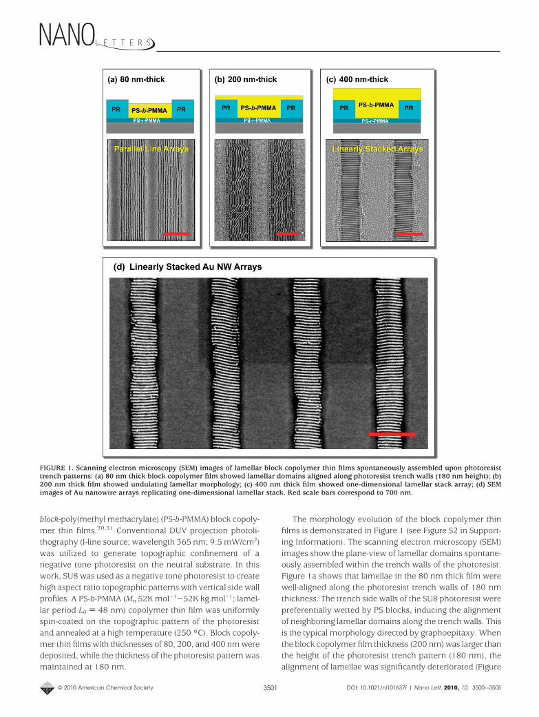
The morphology evolution of the block copolymer thinfilms is demonstrated in Figure 1 (see Figure S2 in Support-ing Information). The scanning electron microscopy (SEM)images show the plane-view of lamellar domains spontane-ously assembled within the trench walls of the photoresist.Figure 1a shows that lamellae in the 80 nm thick film werewell-aligned along the photoresist trench walls of 180 nmthickness. The trench side walls of the SU8 photoresist werepreferentially wetted by PS blocks, inducing the alignmentof neighboring lamellar domains along the trench walls. Thisis the typical morphology directed by graphoepitaxy. Whenthe block copolymer film thickness (200 nm) was larger thanthe height of the photoresist trench pattern (180 nm), thealignment of lamellae was significantly deteriorated (Figure
FIGURE 1. Scanning electron microscopy (SEM) images of lamellar block copolymer thin films spontaneously assembled upon photoresisttrench patterns: (a) 80 nm thick block copolymer film showed lamellar domains aligned along photoresist trench walls (180 nm height); (b)200 nm thick film showed undulating lamellar morphology; (c) 400 nm thick film showed one-dimensional lamellar stack array; (d) SEMimages of Au nanowire arrays replicating one-dimensional lamellar stack. Red scale bars correspond to 700 nm.
© 2010 American Chemical Society 3501 DOI: 10.1021/nl101637f | Nano Lett. 2010, 10, 3500-–3505
1b). Interestingly, one-dimensional dot arrays appeared atthe interface with the trench sidewall, while the blockcopolymer lamellae are undulated in the central region ofthe trench. Meanwhile, when the block copolymer filmthickness was further increased up to 400 nm (Figure 1c), asurprising morphology evolution occurred. Block copolymerlamellar domains are oriented perpendicular to both thetrench sidewall and the substrate. This peculiar morphologyevolution of one-dimensional lamellar stack is hardly antici-pated in a graphoepitaxial approach. As commented above,the typical graphoepitaxy generates the lamellar alignmentalong the trench side wall. Previously, there have beenseveral reports associated to the formation of a one-dimensional “nanocylinder” array, where the orientation ofsurface parallel cylinders is perpendicular to the structuredirecting trench pattern. Those behaviors were attributed tothe flow induced orientation,32,33 which hardly occurs in thefilm with thickness larger than the height of the photoresisttrench.34
Figure 1d shows Au nanowire array prepared by usingthe one-dimensional lamellar stack morphology as a tem-plate. Oxygen reactive etching (RIE) was used to selectivelyremove PMMA from the lamellar stack morphology and tosufficiently reduce the remaining PS lamellar height (60-80nm). Au nanowire array was prepared by Au deposition overthe entire area and subsequent lift-off of the block copolymerfilm and photoresist trench pattern. Taking advantage of thedisposable photoresist pattern, a one-dimensional nanowirestack that exactly replicated the block copolymer film mor-phology was created without any damage of underlying flatsilicon substrate. This pattern transferred morphology gen-erated by a conventional lift-off process provides directevidence that the one-dimensional lamellar stack morphol-ogy is penetrating throughout the block copolymer film withthickness of about 400 nm.
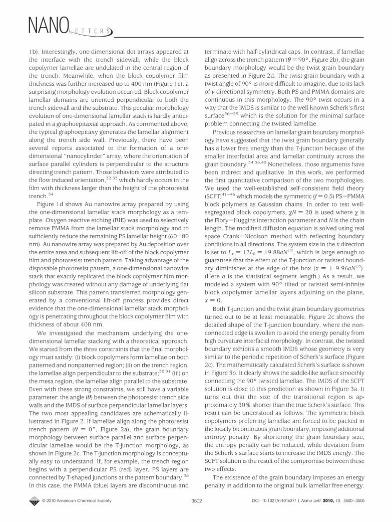
We investigated the mechanism underlying the one-dimensional lamellar stacking with a theoretical approach.We started from the three constraints that the final morphol-ogy must satisfy: (i) block copolymers form lamellae on bothpatterned and nonpatterned region; (ii) on the trench region,the lamellae align perpendicular to the substrate;30,31 (iii) onthe mesa region, the lamellae align parallel to the substrate.Even with these strong constraints, we still have a variableparameter: the angle (θ) between the photoresist trench sidewalls and the IMDS of surface perpendicular lamellar layers.The two most appealing candidates are schematically il-lustrated in Figure 2. If lamellae align along the photoresisttrench pattern (θ ) 0°, Figure 2a), the grain boundarymorphology between surface parallel and surface perpen-dicular lamellae would be the T-junction morphology, asshown in Figure 2c. The T-junction morphology is conceptu-ally easy to understand. If, for example, the trench regionbegins with a perpendicular PS (red) layer, PS layers areconnected by T-shaped junctions at the pattern boundary.35
In this case, the PMMA (blue) layers are discontinuous and
terminate with half-cylindrical caps. In contrast, if lamellaealign across the trench pattern (θ ) 90°, Figure 2b), the grainboundary morphology would be the twist grain boundaryas presented in Figure 2d. The twist grain boundary with atwist angle of 90° is more difficult to imagine, due to its lackof y-directional symmetry. Both PS and PMMA domains arecontinuous in this morphology. The 90° twist occurs in away that the IMDS is similar to the well-known Scherk’s firstsurface36-39 which is the solution for the minimal surfaceproblem connecting the twisted lamellae.
Previous researches on lamellar grain boundary morphol-ogy have suggested that the twist grain boundary generallyhas a lower free energy than the T-junction because of thesmaller interfacial area and lamellar continuity across thegrain boundary.34,35,40 Nonetheless, those arguments havebeen indirect and qualitative. In this work, we performedthe first quantitative comparison of the two morphologies.We used the well-established self-consistent field theory(SCFT)41-46 which models the symmetric (f ) 0.5) PS-PMMAblock polymers as Gaussian chains. In order to test well-segregated block copolymers, �N ) 20 is used where � isthe Flory-Huggins interaction parameter and N is the chainlength. The modified diffusion equation is solved using realspace Crank-Nicolson method with reflecting boundaryconditions in all directions. The system size in the x directionis set to Lx ) 12L0 ) 19.88aN1/2, which is large enough toguarantee that the effect of the T-junction or twisted bound-ary diminishes at the edge of the box (x ) ( 9.96aN1/2).(Here a is the statistical segment length.) As a result, wemodeled a system with 90° tilted or twisted semi-infiniteblock copolymer lamellar layers adjoining on the plane,x ) 0.
Both T-junction and the twist grain boundary geometriesturned out to be at least metastable. Figure 2c shows thedetailed shape of the T-junction boundary, where the non-connected edge is swollen to avoid the energy penalty fromhigh curvature interfacial morphology. In contrast, the twistedboundary exhibits a smooth IMDS whose geometry is verysimilar to the periodic repetition of Scherk’s surface (Figure2c). The mathematically calculated Scherk’s surface is shownin Figure 3b. It clearly shows the saddle-like surface smoothlyconnecting the 90° twisted lamellae. The IMDS of the SCFTsolution is close to this prediction as shown in Figure 3a. Itturns out that the size of the transitional region is ap-proximately 30% shorter than the true Scherk’s surface. Thisresult can be understood as follows. The symmetric blockcopolymers preferring lamellae are forced to be packed inthe locally bicontinuous grain boundary, imposing additionalentropy penalty. By shortening the grain boundary size,the entropy penalty can be reduced, while deviation fromthe Scherk’s surface starts to increase the IMDS energy. TheSCFT solution is the result of the compromise between thesetwo effects.
The existence of the grain boundary imposes an energypenalty in addition to the original bulk lamellar free energy.
© 2010 American Chemical Society 3502 DOI: 10.1021/nl101637f | Nano Lett. 2010, 10, 3500-–3505

The energy penalty is quantitatively given in terms of theeffective surface tension associated to each grain boundary.By comparing the free energy values of the two systems, wefind that the effective surface tension for the twist grainboundary (θ ) 90°), γTGB ) 4.9 × 10⁻⁴aF0/N1/2 kBT, is lessthan the half of surface tension for the T-junction (θ ) 0°),γTJ ) 1.0 × 10⁻³ aF0/N1/2 kBT. This difference is large enoughto suppress the T-junction and, thus, strongly supports themorphology evolution observed in Figure 1. The ultimatestability of twist grain boundary was confirmed by thecalculations for other possible morphologies at intermediatetilting angles (0° < θ < 90°). Those intermediate morphol-ogies turned out to impose effective surface tensions be-tween γTJ and γTGB. For the 80 nm thick film, polymers resideonly within the trench pattern, and hence the PS domain,preferentially wetting the side wall lay parallel to the patternboundary. In contrast, the mechanism described abovedominates the 400 nm thick film, where a considerably large
FIGURE 2. Two representative orientations of surface perpendicular lamellae assembled within photoresist trenches and the correspondinggrain boundary geometries. Lamellae oriented (a) parallel to the photoresist trench (θ ) 0°) and (b) across the photoresist trench (θ ) 90°).(c) T-junctions and (d) twist grain boundaries calculated by self-consistent field theory (SCFT). Upper figures show the distribution of PS (red)and PMMA (blue) components. The transitional region is colored yellow and green. The exact intermolecular dividing surface (IMDS) is visualizedin the bottom figures.
FIGURE 3. (a) The IMDS of twist grain boundary predicted by theSCFT solution. (b) IMDS according to the Scherk’s minimal surfacemodel. Only 1/4 period of the block copolymer domain is shown inthe y and z direction. At x ) -∞ and x ) ∞, the IMDS is parallel tothe xy and xz plane, respectively.
© 2010 American Chemical Society 3503 DOI: 10.1021/nl101637f | Nano Lett. 2010, 10, 3500-–3505
area of grain boundary between surface perpendicular andsurface parallel lamellae resides above the photoresist trenchpattern. The morphology observed for the 200 nm thick filmis in the transitional regime.
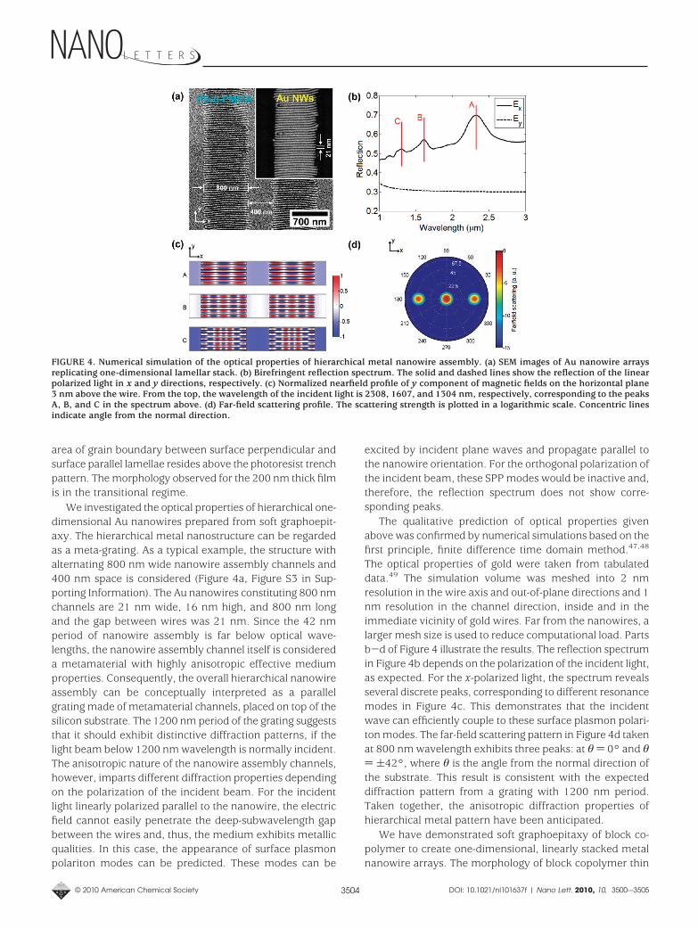
We investigated the optical properties of hierarchical one-dimensional Au nanowires prepared from soft graphoepit-axy. The hierarchical metal nanostructure can be regardedas a meta-grating. As a typical example, the structure withalternating 800 nm wide nanowire assembly channels and400 nm space is considered (Figure 4a, Figure S3 in Sup-porting Information). The Au nanowires constituting 800 nmchannels are 21 nm wide, 16 nm high, and 800 nm longand the gap between wires was 21 nm. Since the 42 nmperiod of nanowire assembly is far below optical wave-lengths, the nanowire assembly channel itself is considereda metamaterial with highly anisotropic effective mediumproperties. Consequently, the overall hierarchical nanowireassembly can be conceptually interpreted as a parallelgrating made of metamaterial channels, placed on top of thesilicon substrate. The 1200 nm period of the grating suggeststhat it should exhibit distinctive diffraction patterns, if thelight beam below 1200 nm wavelength is normally incident.The anisotropic nature of the nanowire assembly channels,however, imparts different diffraction properties dependingon the polarization of the incident beam. For the incidentlight linearly polarized parallel to the nanowire, the electricfield cannot easily penetrate the deep-subwavelength gapbetween the wires and, thus, the medium exhibits metallicqualities. In this case, the appearance of surface plasmonpolariton modes can be predicted. These modes can be
excited by incident plane waves and propagate parallel tothe nanowire orientation. For the orthogonal polarization ofthe incident beam, these SPP modes would be inactive and,therefore, the reflection spectrum does not show corre-sponding peaks.
The qualitative prediction of optical properties givenabove was confirmed by numerical simulations based on thefirst principle, finite difference time domain method.47,48
The optical properties of gold were taken from tabulateddata.49 The simulation volume was meshed into 2 nmresolution in the wire axis and out-of-plane directions and 1nm resolution in the channel direction, inside and in theimmediate vicinity of gold wires. Far from the nanowires, alarger mesh size is used to reduce computational load. Partsb-d of Figure 4 illustrate the results. The reflection spectrumin Figure 4b depends on the polarization of the incident light,as expected. For the x-polarized light, the spectrum revealsseveral discrete peaks, corresponding to different resonancemodes in Figure 4c. This demonstrates that the incidentwave can efficiently couple to these surface plasmon polari-ton modes. The far-field scattering pattern in Figure 4d takenat 800 nm wavelength exhibits three peaks: at θ ) 0° and θ) (42°, where θ is the angle from the normal direction ofthe substrate. This result is consistent with the expecteddiffraction pattern from a grating with 1200 nm period.Taken together, the anisotropic diffraction properties ofhierarchical metal pattern have been anticipated.
We have demonstrated soft graphoepitaxy of block co-polymer to create one-dimensional, linearly stacked metalnanowire arrays. The morphology of block copolymer thin
FIGURE 4. Numerical simulation of the optical properties of hierarchical metal nanowire assembly. (a) SEM images of Au nanowire arraysreplicating one-dimensional lamellar stack. (b) Birefringent reflection spectrum. The solid and dashed lines show the reflection of the linearpolarized light in x and y directions, respectively. (c) Normalized nearfield profile of y component of magnetic fields on the horizontal plane3 nm above the wire. From the top, the wavelength of the incident light is 2308, 1607, and 1304 nm, respectively, corresponding to the peaksA, B, and C in the spectrum above. (d) Far-field scattering profile. The scattering strength is plotted in a logarithmic scale. Concentric linesindicate angle from the normal direction.
© 2010 American Chemical Society 3504 DOI: 10.1021/nl101637f | Nano Lett. 2010, 10, 3500-–3505
films was determined by their tendency to form twist grainboundary and thereby minimize the free energy. Accord-ingly, they are controllable by changing the relative thicknessof block copolymer films with respect to the height ofdisposable topographic confinement. We note that our softgraphoepitaxy is greatly advantageous for pattern transferand further overlay process, since the structure directingphotoresist pattern is readily removable by a mild cleaningprocess. The optical properties of a hierarchical gold nano-wire assembly prepared from the soft graphoepitaxy of thickblock copolymer films have been investigated by first prin-ciple calculations. Highly anisotropic optical propertiescoupled with a surface plasmon polariton and the diffractionoriginating from the parallel grating configuration areanticipated.
Acknowledgment. This work was supported by the Na-tional Research Laboratory Program (R0A-2008-000-20057-0), the National Research Foundation of Korea (NRF) grant(No. K20722000002-10B0100-00210, No. 2009-0089230,2008-0062204), Center for Nanoscale Mechatronics & Manu-facturing, one of the 21st Century Frontier Research Pro-grams (2010K000163), and the Platform Project Grant(10033636-2009-11) supported by the Korean government(MEST & MKE). J.S. thanks the TJ Park Postdoctoral Fellow-ship for financial support.
Supporting Information Available. Experimental meth-ods and supporting results. This material is available free ofcharge via the Internet at http://pubs.acs.org.
REFERENCES AND NOTES(1) Hawker, C. J.; Russell, T. P. MRS Bull. 2005, 30, 952.(2) Tang, C.; Lennon, E. M.; Fredrickson, G. H.; Kramer, E. J.; Hawker,
K. J. Science 2008, 322, 429.(3) Park, M.; Harrison, C.; Chaikin, P. M.; Register, R. A.; Adamson,
D. H. Science 1997, 276, 1401.(4) Thurn-Albrecht, T.; Schotter, J.; Kastle, G. A.; Emley, N.; Shibauchi,
T.; Krusin-Elbaun, L.; Guarini, K.; Black, C. T.; Tuominen, M. T.;Russell, T. P. Science 2000, 290, 2126.
(5) Kim, B. H.; Shin, D. O.; Jeong, S.-J.; Koo, C. M.; Jeon, S. C.; Hwang,W. J.; Lee, S.; Lee, M. G.; Kim, S. O. Adv. Mater. 2008, 20, 2303.
(6) Kim, B. H.; Lee, H. M.; Lee, J.-H.; Son, S.-W.; Jeong, S.-J.; Lee, S. M.;Lee, D. I.; Kwak, S. W.; Jeong, H. W.; Shin, H. J.; Yoon, J.-B.;Lavrentovich, O. D.; Kim, S. O. Adv. Funct. Mater. 2009, 19, 2584.
(7) Zhao, Y.; Thorkelsson, K.; Mastroianni, A. J.; Schilling, T.; Luther,J. M.; Rancatore, B. J.; Matsunaga, K.; Jinnai, H.; Wu, Y.; Poulsen,D.; Frechet, J. M. J.; Alivisatos, A. P.; Xu, T. Nat. Mater. 2009, 8,979.
(8) Kim, S. O.; Solak, H. H.; Stoykovich, M. P.; Ferrier, N. J.; De Pablo,J. J.; Nealey, P. F. Nature 2003, 424, 411.
(9) Ruiz, R.; Kang, H.; Detcheverry, F. A.; Dobisz, E.; Kercher, D. S.;Albrecht, T. R.; de Pablo, J. J.; Nealey, P. F. Science 2008, 321,936.
(10) Kim, S. O.; Kim, B. H.; Meng, D.; Shin, D. O.; Koo, C. M.; Solak,H. H.; Wang, Q. Adv. Mater. 2007, 19, 3271.
(11) Bita, I.; Yang, J. K. W.; Jung, Y. S.; Ross, C. A.; Thomas, E. L.;Berggren, K. K. Science 2008, 321, 939.
(12) Segalman, R. A.; Yokoyama, H.; Kramer, E. J. Adv. Mater. 2001,13, 1152.
(13) Park, S. M.; Stoykovich, M. P.; Ruiz, R.; Zhang, Y.; Black, C. T.;Nealey, P. F. Adv. Mater. 2007, 19, 607.
(14) Ruiz, R.; Ruiz, N.; Zhang, Y.; Sandstrom, R. L.; Black, C. T. Adv.Mater. 2007, 19, 2157.
(15) Sundrani, D.; Darling, S. B.; Sibener, S. J. Nano Lett. 2004, 4, 273.(16) Cheng, J. Y.; Mayes, A. M.; Ross, C. A. Nat. Mater. 2004, 3, 823.(17) Park, S.; Lee, D. H.; Xu, J.; Kim, B.; Hong, S. W.; Jeong, U.; Xu,
T.; Russell, T. P. Science 2009, 20, 1030.(18) Cheng, J. Y.; Ross, C. A.; Chan, V. Z.-H.; Thomas, E. L.; Lam-
merink, R. G. H.; Vancso, G. J. Adv. Mater. 2001, 13, 1174.(19) Black, C. T.; Ruiz, R.; Breyta, G.; Cheng, J. Y.; Colburn, M. C.;
Guarini, K. W.; Kim, H.-C.; Zhang, Y. IBM J. Res. Dev. 2007, 51,605.
(20) Maier, S. A.; Brongersma, M. L.; Kik, P. G.; Meltzer, S.; Requicha,A. A. G.; Atwater, H. A. Adv. Mater. 2001, 13, 1501.
(21) Jeong, S.-J.; Kim, J. E.; Moon, H.-S.; Kim, B. H.; Kim, S. M.; Kim,J. B.; Kim, S. O. Nano Lett. 2009, 9, 2300.
(22) Barnes, W. L.; Dereux, A.; Ebbesen, T. W. Nature (London) 2003,424, 824.
(23) Maier, S. A.; Kik, P. G.; Atwater, H. A.; Meltzer, S.; Harel, E.; Koel,B. E.; Requicha, A. A. G. Nat. Mater. 2003, 2, 229.
(24) Cowburn, R. P.; Welland, M. E. Science 2000, 287, 1466.(25) Imre, A.; Csaba, G.; Ji, L.; Orlov, A.; Bernstein, G. H.; Porod, W.
Science 2006, 311, 205.(26) Ross, C. A. Annu. Rev. Mater. Res. 2001, 31, 203.(27) Pompa, P. P.; Martiradonna, L.; Della Torre, A.; Della Sala, F.;
Manna, L.; de Vittorio, M.; Calabi, F.; Cingolani, R.; Rinaldi, R.Nat. Nanotechnol. 2006, 1, 126.
(28) Demers, L. M.; Ginger, D. S.; Park, S.-J.; Li, Z.; Chung, S.-W.;Mirkin, C. A. Science 2002, 296, 1836.
(29) Lee, S.; Shin, J.; Lee, Y.-H.; Fan, S.; Park, J.-K. Nano Lett. 2010,10, 296.
(30) Mansky, P.; Liu, Y.; Huang, E.; Russell, T. P.; Hawker, C. Science1997, 275, 1458.
(31) Jeong, S.-J.; Xia, G.; Kim, B. H.; Shin, D. O.; Kwon, S.-H.; Kang,S.-W.; Kim, S. O. Adv. Mater. 2008, 20, 1898.
(32) Jung, Y. S.; Ross, C. A. Nano Lett. 2007, 7, 2046.(33) Sundrani, D.; Darling, S. B.; Sibener, S. J. Langmuir 2004, 20,
5091.(34) Shin, D. O.; Kim, B. H.; Kang, J.-H.; Jeong, S.-J.; Park, S. H.; Lee,
Y.-H.; Kim, S. O. Macromolecules 2009, 42, 1189.(35) Duque, D.; Katsov, K.; Schick, M. J. Chem. Phys. 2002, 117, 10315.(36) Thomas, E. L.; Anderson, D. M.; Henkee, C. S.; Hoffman, D.
Nature 1988, 334, 598.(37) Gido, S. P.; Gunther, J.; Thomas, E. L. Macromolecules 1993, 26,
4506.(38) Kyrylyuk, A. V.; Fraaije, J. G. E. M. Macromolecules 2005, 38, 8546.(39) Kamien, R. D.; Lubensky, T. C. Phys. Rev. Lett. 1999, 82, 2892.(40) Gido, S. P.; Thomas, E. L. Macromolecules 1994, 27, 6137.(41) Matsen, M. W. J. Phys.:Condens. Matter. 2002, 14, R21.(42) Drolet, R.; Fredrickson, G. H. Phys. Rev. Lett. 1999, 83, 4317.(43) Kim, J. U.; Matsen, M. W. Soft Matter 2009, 5, 2889.(44) Kim, J. U.; Matsen, M. W. Phys. Rev. Lett. 2009, 102, No. 078303.(45) Kim, J. U.; Matsen, M. W. Macromolecules 2008, 41, 246.(46) Kim, J. U.; Matsen, M. W. Macromolecules 2008, 41, 4435.(47) Fan, S.; Villeneuve, P. R.; Joannopoulos, J. D. Phys. Rev. B 1996,
54, 11245.(48) Shin, J.; Shen, J.-T.; Fan, S. Phys. Rev. Lett. 2009, 102, No. 093903.(49) Handbook of Optical Constants of Solids; Palik, E. D., Ed.; Aca-
demic: Orlando, FL, 1985.
© 2010 American Chemical Society 3505 DOI: 10.1021/nl101637f | Nano Lett. 2010, 10, 3500-–3505