on the use of slots in the design of patch antennas
TRANSCRIPT

1
A PERSONAL OVERVIEW OF THE DEVELOPMENT OF PATCH ANTENNAS
Part 1
Kai Fong Lee
Dean Emeritus, School of Engineering and Professor Emeritus, Electrical Engineering, University of Mississippi
and
Professor Emeritus, Electrical Engineering, University of
Missouri-Columbia
October 28, 2015
City University of Hong Kong

2
Abstract
This four-hour talk is a personal account of the development of microstrip patch antennas. It begins with how the speaker, with a background in theoretical plasma physics, got into the study of patch antennas in the early 1980’s. After a review of basic theory, the speaker’s involvement in the development of patch antenna design through research on various topics is described. These include basic characteristics, broadbanding and size-reduction techniques, full wave analysis, dual and triple band designs, circularly polarized as well as reconfigurable patch antennas. Highlighted in the presentation is the close collaboration with the Department of Electronic Engineering at the City University of Hong Kong through the years. The talk ends with a brief assessment of our impact in the field.

3
Outline 1. How I got into patch antenna research 2. Basic geometry and basic characteristics of patch antennas 3. Our first topic 4. Our research on topics related to basic studies 5. Broadbanding techniques 6. Full wave analysis and CAD formulas 7. Dual/triple band designs 8. Designs for circular polarization 9. Reconfigurable patch antennas 10. Size reduction techniques 11. Concluding remarks and some citation data

Schedule
4
Part 1
(Hour 1)
Part 2
(Hour 2)
Part 3
(Hour 3)
Part 4
(Hour 4)
1. How I got into patch
antenna research
2. Basic geometry and
basic characteristics of
patch antennas
3. Our first topic
4. Our research on topics
related to basic studies
5. Broadbanding
techniques
6. Full wave analysis and
CAD formulas
7. Dual/triple band
designs
8. Designs for circular
polarization
9. Reconfigurable patch
antennas
10. Size reduction
techniques
11. Concluding remarks
and some citation data

5
Main Reference

1. How I got into research on patch antennas
● Research from 1965-1980: Theoretical plasma
physics. 50 journal papers in physics journals
● First antenna papers: 1981; based on senior projects
of CUHK students
● Attended 1981 IEEE AP meeting in Los Angeles;
first exposed to papers on patch antenna research
● Had an idea on flight back to HK; teamed up with
Dr. J. Dahele on patch antenna research.
● All subsequent papers (with many collaborators) were on
patch antennas- no more on plasmas.

1981 AP-S Meeting in Los Angeles: Two sessions on microstrip antennas

COLLABORATORS
Topic Collaborators
CUHK City Univ.
Univ. Akron
NASA Univ. Toledo
Univ. Missouri
Univ. Mississippi
Basic Studies
Ho, Yeung, Wong, Dr. Dahele
Prof. Luk Huynh
Broadbanding
Tong, Mak, Guo, Prof. Luk
Huynh, Bobinchak
Dr. R. Lee
Full wave analysis and CAD formulas
Chen, Fan
Small-size wideband
Chair, Prof. Luk
Shackelford Chair
(To be continued)

COLLABORATORS (continued)
Topic Collaborators
CUHK City Univ. Univ. Akron
NASA Univ. Toledo
Univ. Missouri
Univ. Mississippi
Circular Polarization
S.Yang, Prof. Luk
Khilde, Nayeri, S.Yang, Prof. Kishk, Profs. F. Yang & Elsherbeni
Dual/Triple Band
S.Yang, Mok, Wong, Prof. Luk
S. Yang, Prof. Kishk
Reconfigurable Ho, Dr. Dahele
S.Yang S. Yang, Khilde, Prof. Elsherbeni, Prof. F. Yang

Fig. 1.1 10
2. Basic Geometry and Basic Characteristics of
Patch Antennas
Patch antenna is a relatively new class of antennas developed over the last three and a half decades. The basic structure consists of an area of metallization supported above a ground plane and fed against the ground at an appropriate location.

Copyright © Dr. Kai-Fong Lee Fig. 1.2
Microstrip line
Coaxial probe Aperture-coupled feed
(not until 1985)
Patch
geometry
Rectangle
Triangle
Ring
Disk
2.1 Basic Geometries
Feeding
methods

Copyright © Dr. Kai-Fong Lee 12
2.2 Advantages and Disadvantages
2.2.1 Advantages
Planar (can also be made conformal to shaped surface)
Low profile
Low radar cross-section
Rugged
Can be produced by printed circuit technology
Can be integrated with circuit elements
Can be designed to perform multiple functions.

Fig.1.3(a) Shuttle imaging radar antennas during flight Fig. 1.3(b) Shuttle imaging radar antennas in laboratory
13
2.2.1 Advantages These advantages make microstrip patch antennas much more suitable for
aircraft, space craft, and missiles as they do not interfere with the
aerodynamics of these moving vehicles.

Copyright © Dr. Kai-Fong Lee 14
Fig.1.4 Conformal microstrip array on wing shape Air Force Research Lab.
Hanscom AFB, USA
Fig. 1.5 Conformal Antenna Array Fraunhofer Institute for High Frequency
Physics and Radar Techniques

Fig. 1.6 Patch antennas in wireless communication systems
2.2.1 Advantages These antennas have also become the favorites of antenna designers for
commercial mobile and wireless communication systems.
Base station antenna array
Antenna in
Pager
Antenna in
cellular phone
Copyright © Dr. Kai-Fong Lee 16
2.2 Advantages and Disadvantages
2.2.2 Disadvantages
In its basic form, the microstrip antenna has a narrow bandwidth, typically less
than 5 %. However, various bandwidth-widening techniques have been
developed. Up to 50 % bandwidths have been achieved. It is generally true that
wider bandwidth is achieved with the sacrifice of increased antenna physical
volume.
The microstrip antenna can handle relatively lower RF power due to the small
separation between the radiating patch and its ground plane. Generally, a few
tens watts of average power or less is considered safe.

Copyright © Dr. Kai-Fong Lee 17
2.2 Advantages and Disadvantages
2.2.2 Disadvantages
While a single patch element generally incurs very little loss because it is only
about one half wave long, microstrip arrays generally have larger ohmic loss
than other types of antennas of equivalent aperture size. This ohmic loss mostly
occurs in the dielectric substrate and the metal conductor of the microstrip line
power dividing circuit.

Copyright © Dr. Kai-Fong Lee 18
2.3 Material Consideration Metallic patch is normally made of thin copper foil.
Purpose of substrate material primarily to provide mechanical support for
the radiating patch elements and to maintain the required spacing
between the patch and its ground plane.
The substrate thickness is in the range of 0.01 to 0.05 free-space
wavelength.
Dielectric constant range from 1 to 10. Can be separated into three
categories:
(1) Having a relative dielectric constant (relative permittivity) in the
range of 1.0 to 2.0. This type of material can be air, Polystyrene
Foam, or dielectric Honeycomb.
(2) Having a relative dielectric constant in the range of 2.0 to 4.0 with
material consisting mostly of Fiber-glass reinforced Teflon.

Copyright © Dr. Kai-Fong Lee 19
(3) With a relative dielectric constant between 4.0 and 10.0. The
material can consist of Ceramic, Quartz, or Alumina.
Most popular is Teflon-based with a relative permittivity between 2 and 3.
The Teflon-based material, also named PTFE (PolyTeraFluoroEthylene),
has a structure form very similar to fiberglass material used for digital
circuit boards, but has a much lower loss tangent.
For commercial application, cost is one of the most important criteria in
determining the substrate. For example, a single patch or an array of a few
elements may be fabricated on a low-cost fiberglass material at the L-band
frequency, while a 20-element array at 30 GHz may have to use higher-
cost, but lower loss, Teflon-based material (loss tangent less than 0.005).

Copyright © Dr. Kai-Fong Lee 20
For a large number of array elements at lower microwave frequencies
(below 15 GHz), a dielectric honeycomb or foam panel may be used as a
substrate to minimize loss, antenna mass, and material cost while having
increased bandwidth performance.
There are materials with relative dielectric constant higher than 10. Patch
size is smaller for higher dielectric constant. However, higher dielectric
constant also reduces bandwidth and radiation efficiency.

Fig. 1.7 Coaxial fed patch antenna
The coax probe is usually 50 . The
location of the probe should be at a
50 point of the patch to achieve
impedance matching
Type N, TNC, or BNC is for VHF,
UHF, or lower microwave
frequencies
OSM or OSSM can be used
throughout microwave frequencies
OSSM, OS-50 or K-connector for
millimeter-wave frequencies
2.4 Feed Methods for Single Element
2.4.1 Coax Probe Feed Circular patch fed
by coax probe
Patch radiator
Substrate
Ground plane
Coax connector
x
z
x
y

Copyright © Dr. Kai-Fong Lee Fig. 1.8
A microstrip patch can be
connected directly to a Microstrip
transmission line.
At the edge of a patch,
impedance is generally much
higher than 50 (e.g. 200 ). To
avoid impedance mismatch,
sections of quarter-wavelength
transformers can be used to
transform a large input impedance
to a 50 line.
2.4 Feed Methods for Single Element
2.4.2 Microstrip-Line Feed
Rectangular patch
fed by microstrip
line
Patch radiator
Substrat
e
Ground
plane
x
z
x
y
Quarter-wave
transformer

Fig. 1.9 Strip-line fed patch antenna 23
Another method of matching the
antenna impedance is to extend the
microstrip line into the patch, as
shown.
2.4 Feed Methods for Single Element
2.4.2 Microstrip-Line Feed
Substrat
e
Ground
plane
Rectangular patch fed
by a recessed
microstrip line
Patch radiator
x
z
x
y With this feed approach, array of patch
elements and their microstrip power
division lines can all be designed and
chemically etched on the same
substrate with relatively low fabrication
cost per element. However, the
leakage radiation of the transmission
lines may be large enough to raise the
sidelobe or cross-polarized levels of
the array radiation.

Copyright © Dr. Kai-Fong Lee 24
An open-ended microstrip line
can be placed on one side of the
ground plane to excite a patch
antenna suited on the other side
through an opening slot in the
ground plane. This slot-coupling
or aperture-coupling technique
can be used to avoid soldering
connection as well as to avoid
leakage radiation of the line to
interfere with the patch radiation.
2.4 Feed Methods for Single Element
2.4.3 Aperture-Coupled Feed (D. M. Pozar 1985)
Fig. 1.10 Aperture-coupled fed patch antenna

Copyright © Dr. Kai-Fong Lee 25
In addition, this feed method allows the patch to achieve wide
bandwidth (>10 %) with a thick substrate. The extra bandwidth that is
achieved by this method when compared to the coax probe feed is
generated by the coupling slot which is also a resonator and a radiator.
When two resonators (slot and patch) having different but closely
spaced resonance, wider bandwidth is achieved.
A disadvantage is the back radiation from the slot.
2.4.3 Aperture-Coupled Feed

Copyright © Dr. Kai-Fong Lee 26
2.4.4 Summary of Advantages and Disadvantages of Feeding
Methods
Advantages Disadvantages
Coaxial Feed •Easy to match
•Low spurious radiation
•Large inductance for thick substrate
•Soldering required
Microstrip Line
•Monolithic
•Easy to fabricate
•Easy to match by controlling Insert position
•Spurious radiation from feed line,
especially for thick substrate when
line width is significant
Aperture Coupled
•Use of two substrates avoids deleterious effect of a
high-dielectric constant substrate on the bandwidth
and efficiency
•No direct contact between feed and patch avoiding
large probe reactance or wide microstrip line
•No radiation from the feed and active devices since a
ground plane separates them from the radiating patch
•Multilayer fabrication required
•Higher backlobe radiation

Copyright © Dr. Kai-Fong Lee 27
2.5 The Cavity Model
The cavity model of the patch antenna was developed by Prof. Y. T.
Lo of the University of Illinois and his associates and reported in two
papers, one in 1979 (Lo et al.) and the other in 1981 (Richard et al.).
It is a physical model based on a number of simplifying assumptions.
It is used extensively before commercial simulation softwares were
available, especially for coaxially fed patch antennas.
We briefly summarize the essential features below.
Prof. Y. T. Lo of the University of Illinois, Urbana Champaign

Copyright © Dr. Kai-Fong Lee 28
2.5.1 The Leady Cavity Consider first the region between the patch and the ground
plane.
t r
Free
space
x
z
z
x
y
Ground
plane
Conductor
patch
This resembles an electromagnetic resonator or cavity, excited by a
coaxial probe. In the usual cavity, the vertical walls are also
conducting walls
Et = 0 Et = 0
The fields inside the conducting box are
obtained by solving Maxwell’s equations
in the region inside the box and
demanding its solutions to satisfy the
boundary conditions of Et = 0 on the top,
bottom, and on its sides.

Copyright © Dr. Kai-Fong Lee 29
This leads to the discrete set of characteristic frequencies or resonant
frequencies and discrete set of field patterns or modes.
In The patch antenna case, the side walls are not enclosed by
conducting walls and the fields inside the cavity can leak out to
space, leading to radiation and an antenna results. Since the
radiation fields can be calculated from the fields at the exit region, we
first need to find the fields in the cavity. To do this, we need to know
what boundary condition to impose on the side (vertical) walls.
It turns out that if the substrate is thin so that t << where is
wavelength, the boundary condition is Ht = 0 on the side walls and
the boundary value problem to solve is
Ht = 0 Ht = 0
Et = 0
Et = 0
Rectangular
shape Et = 0
Ht = 0
General
shape

2.6 Basic characteristics In the late 1970’s and 1980’s, the cavity model was used to predict the basic characteristics of the probe-fed rectangular, circular, annular-ring and equitriangular patch antennas, and the results were verified experimentally. While differing in detail, there are a number of similar features, irrespective of the shapes of the patch. To be specific, the essential features are delineated below for the coaxially fed (also known as probe fed) rectangular patch shown in Fig. 11.
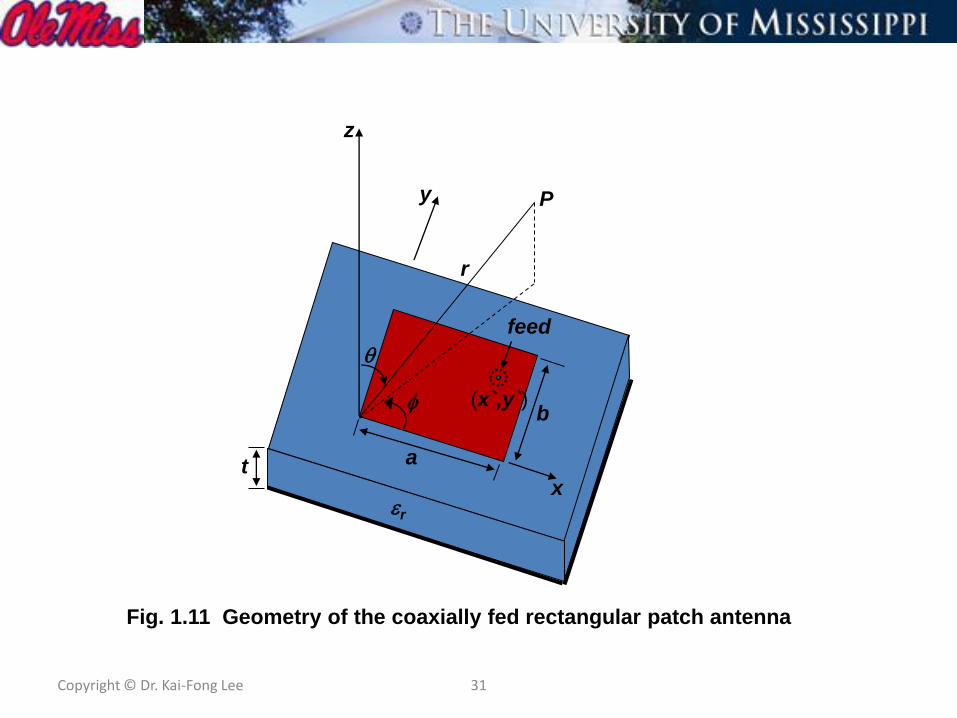
Copyright © Dr. Kai-Fong Lee 31
a
b
r
t x
y
z
P
r
Fig. 1.11 Geometry of the coaxially fed rectangular patch antenna
(x`,y`)
feed

A. The fields under the cavity are transverse magnetic, with the electric field in the z direction and independent of z. There are an infinite number of modes, each characterized by a pair of integers (m, n):
0 cos cosz
m x n yE E
a b
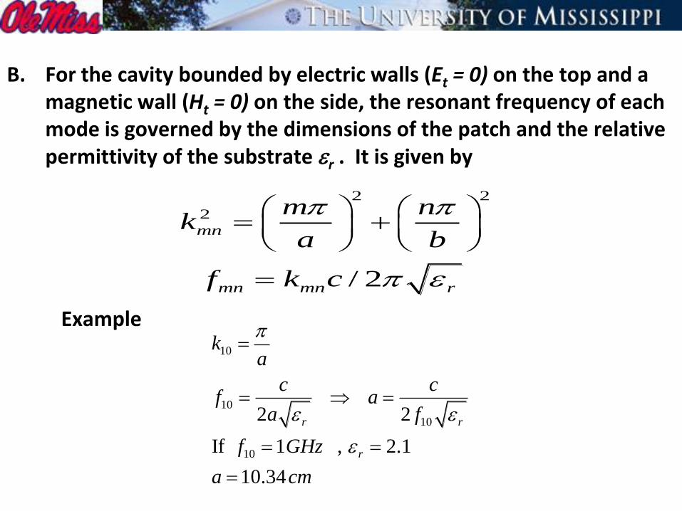
B. For the cavity bounded by electric walls (Et = 0) on the top and a magnetic wall (Ht = 0) on the side, the resonant frequency of each mode is governed by the dimensions of the patch and the relative permittivity of the substrate r . It is given by
Example
2 2
2
/ 2
mn
mn mn r
m nk
a b
f k c
10
10
10
10
2 2
If 1 , 2.1
10.34
r r
r
ka
c cf a
a f
f GHz
a cm

C. Because of fringing fields at the edge of the patch, the patch behaves as if it has a slightly larger dimension. Semi-empirical correction factors are usually introduced in the cavity-model-based design formulas to account for this effect, as well as the fact that the dielectric above the patch (usually air) is different from the dielectric under the patch. These factors vary from patch to patch.
For the rectangular patch, with a > b, a commonly used formula for the fundamental mode, accurate to within 3% of measured values, is
where
is the effective permittivity.
2r
e
cf
a t
1
21 1 101
2 2
r r
e
t
b

D. The equivalent sources at the exit region (the vertical side walls) are the surface magnetic current densities, related to the tangential electric fields in those locations. The tangential electric field (or magnetic surface current distributions) on the side walls for the lowest two modes, TM01 and TM10 , are illustrated in Fig. 12. For the TM10 mode, the magnetic currents along b are constant and in phase while those along a vary sinusoidally and are out of phase. For this reason, the “b” edge is known as the radiating edge since it contributes predominantly to the radiation. The “a” edge is known as the non-radiating edge. Similarly, for the TM01 mode, the magnetic currents are constant and in phase along a and are out of phase and vary sinusoidally along b. The “a” edge is thus the radiating edge for the TM01 mode.
Fig.1.12 Tangential electric field on the side walls of the cavity under the rectangular patch.

E. To satisfy the boundary condition imposed by the feed, the fields under the patch are expressed as a summation of the various modes. The mode with resonant frequency equal to the excitation frequency will be at resonance and has the largest amplitude. Its polarization is called co-polarization. If the off-resonant modes have polarizations orthogonal to the polarization of the resonant mode, they contribute to the cross-polarization.
F. Each resonant mode has its own characteristic radiation pattern. For the rectangular patch, the commonly used modes are TM10 or TM01 . However, the TM03 mode has also received some attention. These three modes all have broadside radiation patterns. The computed patterns for a=1.5b and two values of r are shown in Fig. 1.13. In the principal planes, the TM01 and TM03 modes have similar linear polarization while that of the TM10 mode is orthogonal to the other two. The patterns do not appear to be sensitive to a/b or t. However, they change appreciably with r . Typical half-power beamwidths of the TM10 and TM01 modes are of the order of 1000 and the gains are typically 5 dBi. The patterns of most of the other modes have maxima off broadside. For example, those of the TM11 mode are illustrated in Fig. 13(g) for r =2.32.
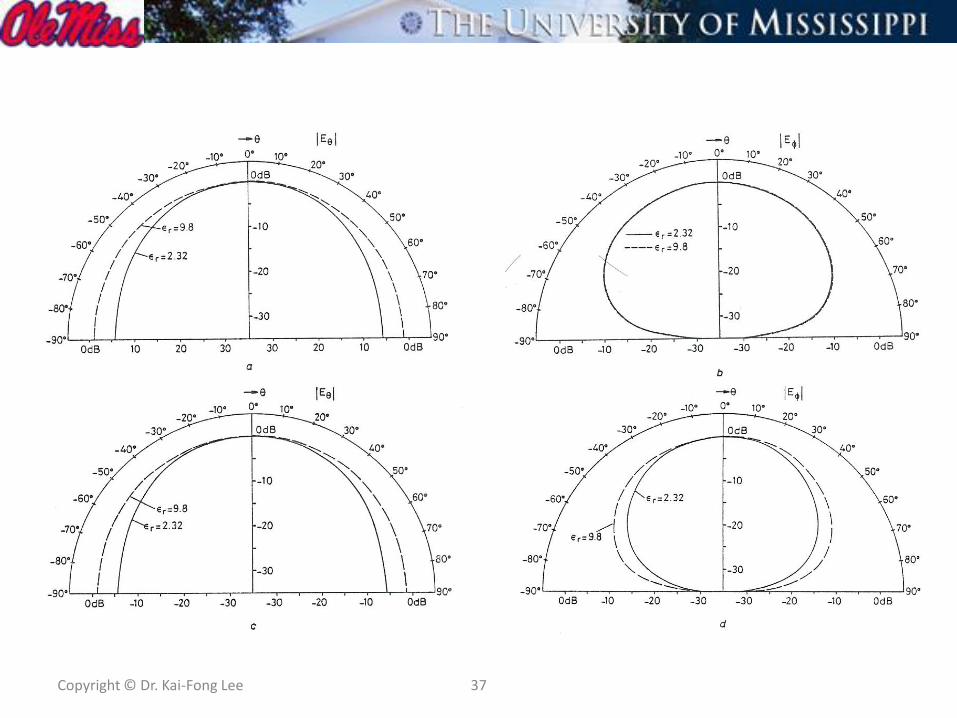
Copyright © Dr. Kai-Fong Lee 37

38
Fig. 1.13 Relative field patterns for a rectangular patch with a/b=1.5, fnm = 1 GHz, and (i) r = 2.32, t=0.318, 0.159, 0.0795
cm; (ii) r = 9.8, t=0.127, 0.0635, 0.0254 cm. (a) TM10, = 0o. (b) TM10, = 90o. (c) TM01, =90o . (d) TM01, = 0o.(e) TM03,
= 90o. (f) TM03, = 0o. (g) TM11, r = 2.32.

For each mode, there are two orthogonal planes in the far field region – one designed as E-plane and the other designed as H-plane. The patterns in these planes are referred to as the E and H plane patterns respectively. One can show from the equations obtained from the cavity model that for the TM01 mode, the y-z plane ( =900 ) is the E-plane and the x-z plane ( =00 ) is the H plane. For the TM10 mode, the x-z plane is the E-plane and the y-z plane is the H plane.
With appropriate design,
circular polarization can be
achieved by utilizing the
two modes. This will be
discussed later. a
b
r
t x
y z P
r
(x`,y`)
feed

G. At resonance, the input reactance is small for thin substrates while the input resistance is largest when the feed is near the edge of the patch and decreases as the feed moves inside the edge. The decrease follows the square of a cosine function for the TM10 and TM01 modes of a coaxial feed rectangular patch. Fig.1.14 shows the theoretical and measured values of the resonant resistance of the first two mode
of a coaxial fed rectangular
patch.
Fig. 1.14 From Lo et al. 1981.

H. By choosing the feed location properly, the resonant resistance can be matched to the feedline resistance, while the use of thin substrates (thickness t < 0.03 λ0 ) will minimize the feed inductance at resonance, resulting in a voltage standing wave ratio (VSWR or SWR) very near unity. As the frequency deviates from resonance, VSWR increases. For linear polarization, a common definition of impedance bandwidth is the range of frequencies for which VSWR is less than or equal to two, corresponding to 10 db return loss or -10 dB for the reflection coefficient S11 . This is usually also the antenna bandwidth, as the patterns are much less sensitive to frequency. For circular polarization, bandwidth is determined by both VSWR < 2 and axial ratio < 3 dB.

I. The losses in the patch antenna comprises radiation, copper, dielectric, and surface wave losses. For thin substrates, surface wave can be neglected. It was found, if the antenna is to launch no more than 25% of the total radiated power as surface waves, the requirement is t/λ0 < 0.07 for r =2.3 and t/λ0 < 0.023 for r=9.8. The quality factor Q of a particular mode is determined by the ratio of the stored to loss energy and determines the impedance bandwidth of the antenna. The larger the losses, the smaller the Q and the larger the bandwidth.
J. In general, the impedance bandwidth is found to increase with substrate thickness t and inversely proportional to r. However, use of low permittivity substrates can lead to high levels of radiation from the feed lines while for higher permittivities, an increase in substrate thickness can lead to decrease in efficiency due to surface wave generation. Additionally, when the substrate thickness exceeds about 0.05 λ0 , where λ0 is free space wavelength, the antenna cannot be matched to the feedline due to the inductance of the feed. As a result, for the basic MPA geometry, the impedance bandwidth is limited to about 5%.

2.7 Limitations of the Cavity Model Analysis
The basic assumption which renders the calculations of the cavity model relatively simple is that the substrate thickness is assumed to be much smaller than wavelength so that the electric field has only a vertical (z) component which does not vary with z. From this it follows that:
(1) The fields in the cavity are TM (transverse magnetic).
(2) The cavity is bounded by magnetic walls (Ht = 0) on the sides.
(3) Surface wave excitation is negligible.
(4) The current in the coaxial probe is independent of z.
The coaxial probe is modeled by a current ribbon of a certain width, which is a free parameter chosen to fit the experimental data.

There are a number of limitations to the cavity model even if the thin substrate condition is satisfied. The magnetic wall boundary condition leads to resonant frequencies which do not agree well with experimental observations, and an ad hoc correction factor has to be introduced to account for the effect of fringing fields. The width of the current ribbon used to model the coaxial probe is another ad hoc parameter. The model cannot handle designs involving parasitic elements, either on the same layer or on another layer. It cannot analyze microstrip antennas with dielectric covers. When the thickness of the substrate exceeds about 2% of the free space wavelength, the cavity model results begin to become inaccurate, due to the breakdown of (1)-(4).
Despite the limitations described above, the cavity model has the advantage of being simple and providing physical insight. In the early 1980’s, it was used to obtain the basic characteristics and design information for rectangular, circular, annular, and triangular patches and compared with measurements.

Copyright © Dr. Kai-Fong Lee 45
REFERENCES Y. T. Lo, D. Solomon, and W. F. Richards, “Theory and experiment on microstrip
antennas,” IEEE Trans. Antennas Propagat., Vol. AP-27, pp. 137-145, 1979.
W. F. Richards, Y. T. Lo and D. D. Harrison, “An improved theory for microstrip
antennas and applications,” IEEE Trans. Antennas Propagat., Vol. AP-29, pp. 38-46,
1981.
K. F. Lee and J. S. Dahele, “Characteristics of microstrip patch antennas and some
methods of improving frequency agility and bandwidth,” in Handbook of Microstrip
Antennas, J. R. James and P. S. Hall (Editors), Peter Peregrinus, Ltd., London, 1989.
C. Wood, “Analysis of microstrip circular patch antennas,” IEE Proc. Vol. 128H, pp.
69-76, 1981.
Copyright © Dr. Kai-Fong Lee 46
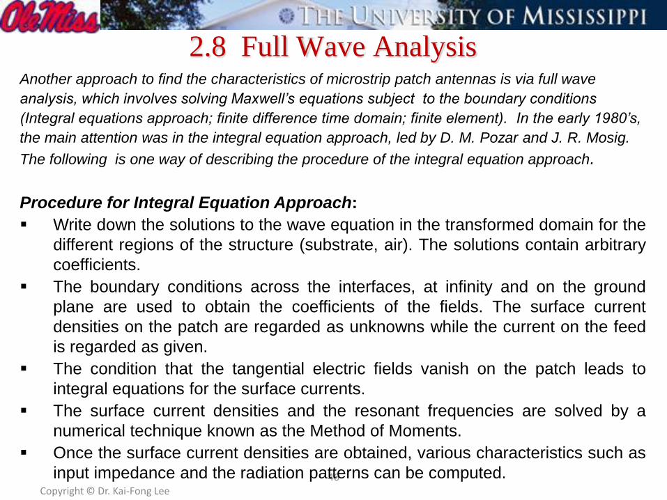
2.8 Full Wave Analysis Another approach to find the characteristics of microstrip patch antennas is via full wave
analysis, which involves solving Maxwell’s equations subject to the boundary conditions
(Integral equations approach; finite difference time domain; finite element). In the early 1980’s,
the main attention was in the integral equation approach, led by D. M. Pozar and J. R. Mosig.
The following is one way of describing the procedure of the integral equation approach.
Procedure for Integral Equation Approach:
Write down the solutions to the wave equation in the transformed domain for the
different regions of the structure (substrate, air). The solutions contain arbitrary
coefficients.
The boundary conditions across the interfaces, at infinity and on the ground
plane are used to obtain the coefficients of the fields. The surface current
densities on the patch are regarded as unknowns while the current on the feed
is regarded as given.
The condition that the tangential electric fields vanish on the patch leads to
integral equations for the surface currents.
The surface current densities and the resonant frequencies are solved by a
numerical technique known as the Method of Moments.
Once the surface current densities are obtained, various characteristics such as
input impedance and the radiation patterns can be computed.

Copyright © Dr. Kai-Fong Lee 47
D. M. Pozar
Advantages of the Full-wave Method
No-AD HOC correction factor
In principle good for thick substrate
Can handle dielectric cover and parasitic elements
Can handle arbitrary patch shape J. R. Mosig
Disadvantages of the Full-wave Method
Need extensive computation time
Little physical insight
In the early 1980’s, use of full-wave method was not
widespread. Commercial simulation softwares based on
full-wave method were not yet available.

2.9 State of patch antenna in the early 1980’s
The state of patch antenna in the early 1980’s can be
partially summarized below:
A. The characteristics of rectangular and circular patches were largely established theoretically (via cavity model) and verified experimentally. However, information on cross polarization characteristics was sketchy.
B. Partial information was obtained for the annular-ring patch and the equitriangular patch.
C. Narrow bandwidth was widely recognized as a problem and interest in frequency tuning and broadbanding techniques began to appear.
D. Full wave methods were being developed.
48

3. Our first topic - Patch antenna with air gap
3.1. Introduction
In many applications, it is necessary for the antenna to receive several adjacent frequencies (e.g. channels). The patch antenna in its basic form is inherently narrow band and may not have the necessary bandwidth. Methods of tuning the operating frequency of the patch antenna are therefore of interest. In 1981 (the time I attended the AP meeting in Los Angeles), there were two methods proposed: (1) using varactor diodes; (2) using shorting posts.

Copyright © Dr. Kai-Fong Lee 50
• For a given set of patch dimensions, the resonant frequency is
primarily governed by the value of the relative permittivity r of the
substrate. If some means is available to alter r , the resonant
frequency will change. One method of achieving this is to introduce
varactor diodes between the patch and the ground plane, as shown in
Fig. 1.15.
• The diodes are provided with a bias voltage, which controls the
varactor capacitance and hence the effective permittivity of the
substrate. Bhartia and Bahl [1982] performed an experiment on this
method and the results are shown in Fig. 1.16.
• The resonant frequency of the lowest mode increases with the bias
voltage. A tuning range of some 20 % was achieved with a 10 V bias.
The range increased to about 30 % with a 30 V bias. The relationship
is not linear.
3.2 Varactor Diodes – Electronic Tuning

Copyright © Dr. Kai-Fong Lee 51
3.2 Varactor Diodes – Electronic Tuning
Fig. 1.15. Illustrating the use of varactor diodes for
tuning.

Copyright © Dr. Kai-Fong Lee 52
3.2 Varactor Diodes – Electronic Tuning
Fig. 1.16. Resonant frequency versus bias voltage for a varctor-loaded rectangular patch
antenna.

Copyright © Dr. Kai-Fong Lee 53
• The value of r can also be changed by introducing shorting posts
(pins) at various points between the patch and the ground plane.
These shorting posts present an inductance, and therefore affect the
effective permittivity of the substrate. The method appeared to be first
introduced by Schaubert et al. in 1981, who performed an experiment
on a rectangular patch using two pins, as shown in Fig. 1.17.
3.3. Tuning Using Shorting Posts (Pins)
Fig. 1.17. Illustrate the use of shorting posts for
tuning the resonant frequency of a patch antenna.

Copyright © Dr. Kai-Fong Lee 54
• The solid curve in Fig.1.18 shows that the resonant frequency is dependent
on the separation of the two posts. A tuning range of some 18 % is
obtained as the separation varies between 0 and the whole width of the
patch.
3.3 Tuning Using Shorting Posts (Pins)
Fig. 1.18 Resonant frequency versus separation of posts for 6.2 9.0 cm rectangular
patch antenna with r = 2.55, t = 1.6 mm.
IE3D

Copyright © Dr. Kai-Fong Lee 55
3.4 Tuning by Means of an Adjustable Air-gap
3.4.1 Geometry of a Microstrip Patch Antenna with Air-Gap
On the flight back from the AP meeting in Los Angeles in 1981, I came
up with the air gap idea to tune the frequency of a patch antenna. The
geometry of a microstrip patch antenna with an air gap is shown in Fig.
18. z
Conducting
patch Substrat
e
r
Spacer
Conducting
plane
Air gap
t
Fig. 1.19 Geometry of a microstrip patch antenna with an air gap

Copyright © Dr. Kai-Fong Lee 56
3.4 Tuning by Means of an Adjustable Air-gap 3.4.1 Geometry of a Microstrip Patch Antenna with Air-Gap
The air gap lowers the effective permittivity of the cavity under the
patch. Hence the resonant frequencies of the various modes will
increase.
The resonant frequencies can be tuned by adjusting the air gap width
.
Substrate and etching tolerances can be compensated by adjusting .
Bandwidth will increase, partly due to the increase in the height of the
dielectric medium and partly because the effective permittivity is now
lower.
Can be applied to patches of arbitrary shape.

Copyright © Dr. Kai-Fong Lee 57
3.4 Tuning by Means of an Adjustable Air-gap 3.4.2 Effective Permittivity – Heuristic Derivation
Consider the capacitance of a capacitor with two dielectric layers,
r1
r2
d1
d2
1 1 1
2 2 2
1 2 1 2 2 1
1 2 1 2 1 2
1 2
1 2 2 1 1 2
1 2 1 2
1 2 2 1
/
/
1 1 1 1
where
eff
eff
C A d A area
C A d
d d d d
C C C A A
AAC
d d d d
d d
d d
Fig. 1.20
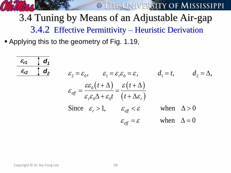
Copyright © Dr. Kai-Fong Lee 58
3.4 Tuning by Means of an Adjustable Air-gap 3.4.2 Effective Permittivity – Heuristic Derivation
Applying this to the geometry of Fig. 1.19,
r1
r2
d1
d2
2 0 1 0 1 2
0
0 0
, , , ,
Since 1, when 0
when 0
r
eff
r r
r eff
eff
d t d
t t
t t

Copyright © Dr. Kai-Fong Lee 59
3.4 Tuning by Means of an Adjustable Air-gap 3.4.3 Theoretical and Experimental Results
The region between the patch and the ground plane is now a two-
layer cavity. The microstrip patch antenna with an air-gap can
therefore be analyzed using the cavity model. The original
assumptions of the cavity model are modified to account for the
two-layers as follows:
(1) Owing to the close proximity between the conducting patch and
the ground plane only transverse magnetic (TM) modes are
assumed to exist. The z-component of the electric field, however, is
a function of z since the cavity is low-layered.
(2) The cavity is assumed to be bounded by perfect electric walls
on the top and on the bottom and by a perfect magnetic wall along
the edge.
(3) Across the dielectric-air interface the tangential electric field and
the normal electric flux density are continuous.

Copyright © Dr. Kai-Fong Lee 60
3.4 Tuning by Means of an Adjustable Air-gap 3.4.3 Theoretical and Experimental Results
Based on the previous assumptions, detailed analysis for coaxially-
fed circular and annular-ring patches with airgaps were carried out
and good agreement between theory and experiment was obtained.
The results were summarized in Dahele and Lee [1985].
In particular, the formula for the resonant frequency is a very simple
one and is given by
0nm
eff
f f
where fnm (0) is the resonant frequency where there is no airgap and
eff is the effective permittivity of the two-layer medium:
eff
r
t
t

Copyright © Dr. Kai-Fong Lee 61
3.4 Tuning by Means of an Adjustable Air-gap 3.4.3 Theoretical and Experimental Results
Note that the formula for eff is identical to the one derived in
section B. The formula for fnm() is valid for any patch shape. As
the airgap width increases, eff decreases and the resonant
frequency increases. The dependence of fnm() on , however, is
not a linear one.

Copyright © Dr. Kai-Fong Lee 62
3.4 Tuning by Means of an Adjustable Air-gap 3.4.3 Theoretical and Experimental Results
Results for a coaxially fed circular patch (Lee, Ho, Dahele; 1984)
Fig. 1.21 (a) Geometry of the antenna (b) Dr. J. S. Dahele and Dr. K. F. Lee, CUHK

Copyright © Dr. Kai-Fong Lee 63
3.4 Tuning by Means of an Adjustable Air-gap 3.4.3 Theoretical and Experimental Results
Results for a circular patch (Lee, Ho, Dahele; 1984):
TM11 1128 MHz 0.89 1286 MHz 1.48 1350 MHz 2.07
TM21 1879 MHz 0.85 2136 MHz 2.15 2256 MHz 2.61
TM31 2596 MHz 0.77 2951 MHz 1.63 3106 MHz 2.02
fnm fnm fnm % BW % BW % BW
= 0 = 0.5
mm
= 1.0
mm
Table 2.1 Measured resonant frequencies and impedance bandwidths of the
first few modes of a 5 cm radius circular-disc antenna with r = 2.32, t =
0.159 cm, fed at 4.75 cm from the center, for three values of the air-gap
width .

Copyright © Dr. Kai-Fong Lee 64
3.4 Tuning by Means of an Adjustable Air-gap 3.4.3 Theoretical and Experimental Results
Results for a circular patch (Lee, Ho, Dahele; 1984):
3106 3082 2951 2911 2596 2571 TM31
2256 2241 2136 2117 1879 1869 TM21
1350 1351 1286 1276 1128 1127 TM11
Calc.
(MHz)
= 0 = 0.5
mm
= 1.0
mm
Table 2.2 Comparison of calculated and measured resonant
frequencies for the circular-disc microstrip antennas.
Meas.
(MHz) Calc.
(MHz)
Meas.
(MHz)
Calc.
(MHz)
Meas.
(MHz)
r = 5.0 cm, t = 0.159 cm, d = 4.75 cm, r = 2.32.

Copyright © Dr. Kai-Fong Lee 65
3.4 Tuning by Means of an Adjustable Air-gap 3.4.3 Theoretical and Experimental Results
Results for a circular patch (Lee, Ho, Dahele; 1984):
Fig. 1.22

66
3.4.4 Advantages of Air Gap Tuning
No need to add components such as varactor diodes or shorting
posts and the associated circuitry
Can be applied to patches of any shape
r
z
h
∆
Spacer
Substrate
Ground
Patch
Air Gap
Problem with probe-feeding
Each time the thickness of the air gap is changed, de-soldering and
re-soldering are needed. This not a problem for aperture coupled
and stripline fed patches.

3.4.5 Aperture coupled and strip-line fed patches
Fig. 1.23 Aperture coupled patch antenna with adjustable airgap

68
W
L
Wf
S
xo
z
h
∆
Air Gap
Substra
te
Ground
Inset-Fed Patch
εr
Fig. 1.24 Stripline fed patch antenna with adjustable airgap

Mao et al. (2011) showed that the adjustable air gap method
for tuning the resonant frequency of a patch antenna with
aperture-coupled feed and stripline feed is found to be
effective. In these cases, changing the air gap width does not
require de-soldering and soldering.
The tuning ranges for coaxial-fed, strip-line fed and
aperture-coupled MPA are similar, which is around 20% for
Δ/h= 0.79. The method is particularly attractive for tuning the resonant
frequency of a multi-element patch antenna array fed by aperture coupling or by strip lines. The resonant frequencies
of all the elements, and therefore of the array, can be tuned by
a single adjustment of the air gap width . This idea, however, remains to be demonstrated.
69

Copyright © Dr. Kai-Fong Lee 70
References on patches with air gap
P. Bhartia, and I. Bahl, “A frequency agile microstrip antenna,” IEEE AP-S Int.
Symp. Digest, pp. 304-307, 1982.
D. H. Schaubert, F. G. Farrar, A. R. Sindoris, and S. T. Hayes, “Microstrip
antennas with frequency agility and polarization diversity,” IEEE Trans. Antennas
Propagat., Vol. AP-29, pp. 118-123, 1981.
K. F. Lee, K. Y. Ho, and J. S. Dahele, “Circular-disk microstrip antenna with an air
gap,” IEEE Trans. Antennas Propagat., Vol. AP-32, pp. 880-884, 1984.
J. S. Dahele, and K. F. Lee, “Theory and experiment on microstrip antennas with
airgaps,” IEE Proc., 132H, pp. 455-460, 1985.
Yilin Mao, Yashwanth R. Padooru, Kai Fong Lee, A. Z. Elsherbeni, and Fan Yang,
“Air gap tuning of patch antenna resonance,” 2011 IEEE AP-S/URSI International
Symposium Digest, Spokane, Washington

71
4. Our research on topics related to basic studies
4.1 The annular-ring patch 4.2 The equitriangular patch 4.3 Cross polarization characteristics of rectangular and circular patches 4.4 Patch on cylindrical surface

Copyright © Dr. Kai-Fong Lee 72
4.1 The Annular-Ring Patch
Fig. 1.25 Geometry of the annular-ring patch
antenna.

Copyright © Dr. Kai-Fong Lee 73
In 1982, W. C. Chew published a full wave analysis of the annular-
ring patch antenna. The main findings concerned the two broadside
modes: the lowest TM11 mode and the higher order TM12 mode:
TM11 mode
Impedance does not vary much with feed position.
Very large resonant resistance; needs matching circuit.
Very narrow bandwidth (1% or less).
TM12 mode
Impedance sensitive to feed position.
With the feed near the inner edge, a good match near 50 can be obtained.
For typical parameters used in practice, the bandwidth is about 4 %, which is several times larger than that of the rectangular and circular patches with the same dielectric constant and thickness.

Copyright © Dr. Kai-Fong Lee 74
Broadside Modes TM11 and TM12
Fig. 1.26 Theoretical input impedance of the TM11 mode of an annular-ring patch antenna
with b = 7.0 cm, a = 3.5 cm, r = 2.32, t = 0.159 cm, fed at two radial locations.

Copyright © Dr. Kai-Fong Lee 75
Broadside Modes TM11 and TM12
Fig. 1.27 Theoretical input impedance of the TM12 mode of an annular-ring patch antenna
with b = 7.0 cm, a = 3.5 cm, r = 2.32, t = 0.159 cm, fed at two radial locations.
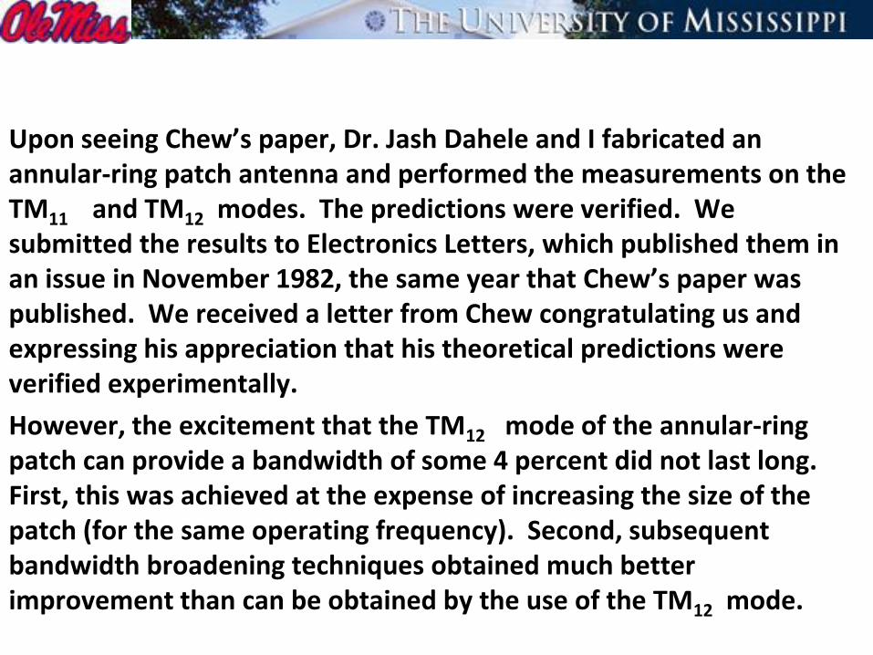
Upon seeing Chew’s paper, Dr. Jash Dahele and I fabricated an annular-ring patch antenna and performed the measurements on the TM11 and TM12 modes. The predictions were verified. We submitted the results to Electronics Letters, which published them in an issue in November 1982, the same year that Chew’s paper was published. We received a letter from Chew congratulating us and expressing his appreciation that his theoretical predictions were verified experimentally.
However, the excitement that the TM12 mode of the annular-ring patch can provide a bandwidth of some 4 percent did not last long. First, this was achieved at the expense of increasing the size of the patch (for the same operating frequency). Second, subsequent bandwidth broadening techniques obtained much better improvement than can be obtained by the use of the TM12 mode.

Copyright © Dr. Kai-Fong Lee 77
4.2 The Equitriangular Patch
Fig. 1.28 Geometry of the equitriangular patch
antenna.

Our contributions:
A. Accurate measurement of resonant frequencies
B. Developed a CAD (computer aided design)
formula for the resonant frequencies
C. A comprehensive cavity model theory for the equitriangular patch, with experimental verification

Table 2.3 Measured resonant frequencies of the first five modes of an equilateral triangular patch antenna with a=10 cm, r=2.32, and thickness 0.159 cm. (Dahele and Lee 1987)
Mode Measured fmn (MHz)
_________________________________
TM10 1280
TM11 2240
TM20 2550
TM21 3400
TM30 3824
_________________________________

Theoretical Resonant Frequency from Cavity Model assuming a perfect magnetic wall:
Question: What correction factor(s) to use to account for the fringing fields and the two-layer dielectric?
In the literature, a number of papers were devoted to answer this question, based mainly on guess work. All of them used our measurements to compare their predictions, and to see whether their correction factor(s) are more accurate than those of others.
1
2 2 22
2 3
mnmn
r r
ck cf m mn n
a

CAD formula for resonant frequency:
In 1992, Chen, Lee and Dahele, instead of guessing, obtained an expression for the effective sidelength ae by curve fitting the data results obtained from full-wave analysis using moment method:
2 2
11 2.199 12.853
1 116.436 6.182 9.802
r
e
r r
h h
a aa a
h h h
a a a
Accuracy of this expression is within 1% when compared with the value
obtained from moment method analysis and with experiment .
The comparisons were carried out for r = 2.32, 0.002 h/0 0.125 and r =
10.0, 0.008 h/0 0.032

When Prof. Luk joined City Polytechnic in June
1985, I asked him to work out a complete cavity-
model-based theory for the equitriangular patch
antenna. We presented the results in the 1986
AP meeting in Philadelphia, and a paper was
published in the AP Transactions in 1988. This
paper has become a standard reference on the
equitriangular patch antenna. 82

83
Prof. K. M. Luk at City Polytechnic in 1985 doing research on the equitriangular patch antenna
Prof. K. M. Luk, Prof. J. S. Dahele and myself at the 1986 AP meeting in Philadelphia, where the paper on the equitriangular patch was presented

Copyright © Dr. Kai-Fong Lee 84
4.3 Cross-Polarization Characteristics of rectangular and
circular patches If a rectangular patch is excited at the resonant frequency of the TM01 mode, the
dominant contribution to the cross-polarized field is the TM10 mode. The higher order
TMm0 modes also contribute, but they will be much weaker than that of the TM10 mode.
The ratio of co-polarization to cross polarization in a particular direction is
approximately given by |E01(,)|/|E10(,)|. Similarly, if the patch is excited at the
resonant frequency of the TM10 mode, it is given approximately by |E10(,)|/|E01(,)|.
For the first case, Oberhart et al. (1989) showed that the cross-polarization level is
dependent on a/b. For a patch fed at the x` = 0 edge, the cross-polarization is smallest
when a/b = 1.5, about 21dB below the co-polarized field.
Extensive studies showing how the co-polarized to cross-polarized ratios depend on
substrate thickness, feed position and resonant frequencies, are given by Huynh, Lee
and Lee (1988) based on the cavity model.
A similar study for the circular patch was carried out using the cavity model by Lee,
Luk and Tam in 1992.
For the rectangular patch, further study using simulation software and performing
measurements, was done by Yang, Lee and Luk in 2008.


4.4 Patch on cylindrical surface
One of the advantages of patch antennas is that they can be mounted on curved surfaces. Example:
We published one of the early papers on patch antennas on cylindrical surfaces in 1989. The theory was worked out by Prof. Luk at City Polytechnic and experimental work was done by Prof. J. S. Dahele at the Royal Military College of Science.
Microstrip array on wing
shape Air Force Research Lab.
Hanscom AFB, USA

Experiment on patch on cylindrical surface was performed by Dr. J. S. Dahele at the Royal Military College of Science,
Shrivenham, UK


Copyright © Dr. Kai-Fong Lee 89
Section 4 References W. C. Chew, “A broad-band annular-ring microstrip antenna,” IEEE Trans. Antennas Propagat., Vol. AP-30,
pp. 918-922, 1982.
J. S. Dahele and K. F. Lee, Characteristics of annular-ring microstrip antenna,
Electronics Letters, 18, 1051-1052, 1982.
K. F. Lee, K. M. Luk, and J. S. Dahele, “Characteristics of the equilateral triangular patch antenna,” IEEE
Trans. Antennas Propagat., Vol. AP-36, pp. 1510-1518, 1988.
J. S. Dahele, and K. F. Lee, “On the resonant frequencies of the triangular patch antenna,” IEEE Trans.
Antennas Propagat., Vol. AP-32, pp. 100-101, 1987.
W. Chen, K. F. Lee, and J. S. Dahele, “Theoretical and experimental studies of the equilateral triangular
patch antenna,” IEEE Trans. Antennas Propagat., Vol. AP-40, pp. 1253-1256, 1992.
M. L. Oberhart, Y. T. Lo, and R. Q. H. Lee, “New simple feed network for an array module of four microstrip
elements,” Electron. Lett. Vol. 23, pp. 436-437, 1987.
T. Huynh, K. F. Lee and R. Q. Lee, Cross polarization characteristics of rectangular
patch antennas, Electronics Letters, Vol. 24, 463-464, 1988.
K.M. Luk, K. F. Lee & J. S. Dahele, Analysis of the cylindrical-rectangular microstrip antenna,
IEEE Transactions on Antennas and Propagation, AP-37, 143-147, 1989.
S. L. S. Yang, K. F. Lee, A. A. Kishk and K. M. Luk, “Cross Polarization Studies of rectangular
patch antenna,” Microwave and Optical Technology Letters, Vol. 50, pp. 2099-2103, 2008.