on device modeling and soft computing for real-time
TRANSCRIPT

PROCEEDINGS
Of
National Conference
On
DEVICE MODELING AND SOFT COMPUTING FOR
REAL-TIME APPLICATIONS
(DMSC-2019)
13th & 14th September 2019
Organized by,
Dept. of Electronics & Communication Engineering
Mallabhum Institute of Technology, Bishnupur, India
In Collaboration with,
The Institution of Engineers India (IEI)

Proceedings of National Conference on Device Modeling and Soft Computing for real time applications (DMSC-2019) Organized by Dept. of ECE, MIT Bishnupur in collaboration with The Institution of Engineers India (IEI)
ABOUT
MALLABHUM INSTITUTE OF TECHNOLOGY, BISHNUPUR
_______________________________________________
ith the mission, to develop the scenario of technical education in the backward region of
West Bengal, a graduate engineering college namely Mallabhum Institute of Technology
was setup in 2002 at Bishnupur. MIT has different streams (CSE, EE, ECE, ME & CE). The
institute approved by AICTE and affiliated to MAKAUT.
In MIT, besides covering the course curriculum both in theory and practice, students are
enabled to face cut-throat competition in this awesome competitive world to surge ahead. Our
college is fully residential; hence the students reap special benefit to interact with teachers
round the clock. Our rich central library with air conditioned reading room, book-bank facilities,
reputed e-journals and internet facilities provide the students a congenial platform of
convergent learning.
MIT is located amidst a tranquil terrain, having sprawling and eco-friendly campus, which offers
a unique environment of study to the engineering students. Apart from academic exercises, wide
scope of participation in different co-curricular activities helps our students to become healthy
citizens in future years.
At MIT, we have redefined and redesigned our teaching-learning process as and when required
to stay tuned and updated in the field of technical education. Continuous effort of our stake
holders at MIT to achieve our goals deserves appreciation. We are sure that our proactive and
able leadership will address all challenges to remain ahead of others amidst tough and volatile
environment in the years to come.
W

Proceedings of National Conference on Device Modeling and Soft Computing for real time applications (DMSC-2019) Organized by Dept. of ECE, MIT Bishnupur in collaboration with The Institution of Engineers India (IEI)
ABOUT
THE INSTITUTION OF ENGINEERS INDIA (IEI)
_______________________________________________
he Institution of Engineers (India) or IEI is the largest multidisciplinary professional body
that encompasses 15 engineering disciplines and gives engineers a global platform from
which to share professional interest. IEI has membership strength of over 0.8 million.
Established in 1920, with its headquarters at 8 Gokhale Road, Kolkata - 700020, IEI has served
the engineering fraternity for over nine decades. In this period of time it has been inextricably
linked with the history of modern-day engineering. In 1935, IEI was incorporated by Royal
Charter and remains the only professional body in India to be accorded this honor. Today, its
quest for professional excellence has given it a place of pride in almost every prestigious and
relevant organization across the globe. IEI functions among professional engineers,
academicians and research workers. It provides a vast array of technical, professional and
supporting services to the Government, Industries, Academia and the Engineering fraternity,
operating from 123 Centres located across the country. IEI provides grant-in-aid to its members
to conduct research and development on engineering subjects. IEI, in collaboration with
Springer, regularly publishes peer-reviewed international journals in five series, covering fifteen
engineering disciplines.
T

Proceedings of National Conference on Device Modeling and Soft Computing for real time applications (DMSC-2019) Organized by Dept. of ECE, MIT Bishnupur in collaboration with The Institution of Engineers India (IEI)
OBJECTIVE OF THE CONFERENCE
Conference Theme: Two days National Conference on Device Modeling and Soft Computing
for real-time applications (DMSC 2019) will basically focus on modeling of electronic devices
and real-time applications of soft-computing. Semiconductor device modeling has developed in
recent years from being solely the domain of device physicists to span broader technological
disciplines involved in device and electronic circuit design and development. Traditional
equivalent circuit models and closed-form analytical models cannot always provide consistently
accurate results for all modes of operation of these very small devices. The desire to move
towards computer aided design and expert systems have reinforced the need for models capable
of representing device operation under DC, small-signal, large-signal and high frequency
operation. It is also desirable to relate the physical structure of the device to the electrical
performance. This demand for better models has led to the introduction of improved equivalent
circuit models and an upsurge in interest in using physical models. Soft computing is based on
natural as well as artificial ideas. Soft Computing is basically optimization technique to find
solution of problems which are very hard to answer. Soft Computing techniques are Fuzzy Logic,
Neural Network, Support Vector Machines, Evolutionary algorithms and Machine Learning,
Probabilistic Reasoning etc. Moreover, Soft Computing techniques, which are based on the
information processing of biological systems are now massively used in the area of pattern
recognition, fuzzy logic, probabilistic reasoning, artificial neural network, making prediction,
planning, as well as acting on the environment.
Sub-Theme: Semiconductor design, Device modeling, System optimization, Manufacturing
systems, Process and System control, Signal & Image processing, Energy management, Solar
Cell, Human Machine Interface, Robotics, Motion control, Power electronics, Green
Computing, Biomedical Engg. and Industrial Electronics.

Proceedings of National Conference on Device Modeling and Soft Computing for real time applications (DMSC-2019) Organized by Dept. of ECE, MIT Bishnupur in collaboration with The Institution of Engineers India (IEI)
PATRONS
Chairperson, Mallabhum Institute of Technology, Bishnupur
Director, Mallabhum Institute of Technology, Bishnupur
Principal, Mallabhum Institute of Technology, Bishnupur
Advisor, Mallabhum Human Resource Development Trust, Bishnupur
ADVISORY COMMITTEE MEMBERS
Dr. Jatindra N. Roy, Adv. Technology Development Centre & School of Energy Science and
Engineering, IIT Kharagpur
Dr. Smarajit Das, EEE Dept., IIT Guwahati
Dr. Anup K. Bhattacharjee, Dept. of ECE, NIT Durgapur
Dr. Ujjal Chakraborty, Dept. of ECE, NIT Silchar
Dr. Kaushik Mandal, Dept. of Radio Physics & Electronics, Calcutta University
Dr. Sujit Das, Dept. of CSE, NIT Warangal
Dr. Joydeep Sengupta, Dept. of ECE, VNIT Nagpur
Dr. Sougata Kumar Kar, Dept. of ECE, NIT Rourkela
Dr. Saikat Ranjan Maity, Dept. of ME, NIT Silchar
Dr. Subhas Ganguly, Dept. of Met. Engineering, NIT Raipur
Dr. Rajendra P. Ghosh, Dept. of Electronics, Vidyasagar University
Dr. Partha Pratim Sarkar, Department of Engineering and Technological Studies (DETS),
University of Kalyani, Kalyani
Dr. Durbadal Mandal, Dept. of ECE, NIT Durgapur
Dr. Indrajit Saha, Dept. of CSE, NITTTR Kolkata
Dr. Debasish Nandi, Dept. of ME, MIT Bishnupur
Dr. Indrani Chakraborty, Dept. of EE, MIT Bishnupur
Dr. Bappadittya Roy, Dept. of ECE, Madanapalle Institute of Technology & Science, Andhra
Pradesh
Mr. Buddhadeb Ghosh, Dept. of S & SS, MIT Bishnupur

Proceedings of National Conference on Device Modeling and Soft Computing for real time applications (DMSC-2019) Organized by Dept. of ECE, MIT Bishnupur in collaboration with The Institution of Engineers India (IEI)
ORGANIZING COMMITTEE MEMBERS
Dr. Khanindra Pathak, Chaiman, IEI, Kharagpur Local Centre
Dr. Pavuluri Srinivasa Rao, Honorary Secretary, IEI, Kharagpur Local Centre
Mrs. Manira Khatun, Dept. of ECE, MIT Bishnupur
Mr. Supratim S. Das, Dept. of ECE, MIT Bishnupur
Mr. Avijit Paul, Dept. of ECE, MIT Bishnupur
Miss. Debashree P. Karmakar, Dept. of ECE, MIT Bishnupur
Mr. Subhajit Bhattacharyya , Dept. of ECE, MIT Bishnupur
Mr. Kausik Chakraborty, Dept. of ECE, MIT Bishnupur
Mrs. Mayumi Mukherjee, Dept. of ECE, MIT Bishnupur
Mr. Suvajit Giri, Dept. of ECE, MIT Bishnupur
CONVENER
Ms. Mousumi Karmakar, HOD, ECE Dept., MIT Bishnupur
PROGRAM CO-ORDINATOR
Mr. Ankan Bhattacharya, ECE Dept., MIT Bishnupur

Proceedings of National Conference on Device Modeling and Soft Computing for real time applications (DMSC-2019) Organized by Dept. of ECE, MIT Bishnupur in collaboration with The Institution of Engineers India (IEI)
LIST OF CONTENTS
Invited Abstracts
HIGHLY SENSITIVE AND SELECTIVE RESISTIVE GAS SENSORS ON MEMS-CMOS
PLATFORM by Dr. Prasanta Kumar Guha ....................................................................................... 1
INTRODUCTION OF GENETIC ALGORITHM IN SOLVING OPTIMIZATION PROBLEMS:
APPLICATION IN EV ENERGY MANAGEMENT by Dr. Arup Kumar Nandi ............................... 2
SCOPE, OPPORTUNITIES AND CHALLENGES OF COPPER (Cu) BASED SEMICONDUCTING
DEVICE IN OPTOELECTRONIC APPLICATIONS by Dr. Ratan Mandal ..................................... 3
NANOTECHNOLOGY FOR DEVICE MODELING AND PHOTONICS APPLICATIONS by
Dr. Arindam Biswas ............................................................................................................................ 5
BIOMEDICAL SENSORDEVICES FOR POINT - OF - CARE DISEASE DIAGNOSIS by
Dr. Gorachand Datta ........................................................................................................................... 6
Technical Papers
ANALYTICAL MODEL FOR A DOPED DOUBLE GATE MOSFET DEVICE BASED ON
CONFORMAL MAPPING TECHNIQUE by Supratim Subhra Das ................................................. 7
STUDY OF THE PERFORMANCE OF DRIVING ASSISTANCE SYSTEM FOR COMPLEX TRIP
PLANNING OF ELECTRIC VEHICLES USING EVOLUTIONARY ALGORITHM by Mousumi
Khanra (Karmakar) and Arup Kr. Nandi ....................................................................................... 14
SOLVING TRAVELLING SALESMAN PROBLEM USING INTUITIONISTIC FUZZY SET
BASED GENETIC ALGORITHM by Amalendu Si and Sujit Das...................................................20
MODELING AND SIMULATION OF A LOW-PROFILE MICROSTRIP PATCH ANTENNA
OPERATING AT 2.45 GHZ by Ankan Bhattacharya ...................................................................... 27
MODELING AND OPTIMIZATION OF A CMPA USING GENETIC ALGORITHM by Arnab De,
Bappadittya Roy, Ankan Bhattacharya and Anup K. Bhattacharjee ........................................... 31
MODELING AND TESTING OF A PRINTED MONOPOLE ANTENNA FOR VARIOUS
WIRELESS APPLICATIONS by Susmita Bala, Partha Pratim Sarkar, Sushanta Sarkar and
Rajendra Prosad Ghosh ..................................................................................................................... 36
DESIGN AND ANALYSIS OF CHEBYSHEV AND BUTTERWORTH FILTERS USING MATLAB
by Manira Khatun and Debashree Patra Karmakar ..................................................................... 41

Proceedings of National Conference on Device Modeling and Soft Computing for real time applications (DMSC-2019) Organized by Dept. of ECE, MIT Bishnupur in collaboration with The Institution of Engineers India (IEI)
MODELING AND PERFORMANCE COMPARISON OF BRUSHLESS DC MOTOR WITH
VARIOUS POLE/SLOT COMBINATION by Soumitra Adak, Mayumi Mukherjee and Sudeshna
Datta .................................................................................................................................................... 45
DC MOTOR SPEED MONITORING SYSTEM USING PID CONTROLLER MODELED
USING LABVIEW by Subham Singha, Santu Shit and Subhajit Bhattacharyya .................... 49
DIFFERENT MODELS OF POWER AMPLIFIER USED IN D.C. CONTROL
ELECTROMAGNETIC LEVITATION SYSTEM by Amit Kundu .................................................... 55
AN AHP MCDM APPROACH FOR SELECTION OF WIND POWER PLANT LOCATION: A
CASE STUDY FROM INDIA by Tilottama Chakraborty and Soumya Ghosh ............................. 62
MODELING OF LAND AND AIR OPERATED ROBOTIC SURVEILLANCE VEHICLE by Arnav
Banerjee, Kausik Chakraborty and Debanjan Sarkar ................................................................... 66
STUDY OF ROUGHNESS OF SURFACES MACHINED BY CNC AND CONVENTIONAL
MACHINING by Swarnangshu Mukhopadhyay, Animesh Nandi, Suman Mandal and
Debasish Nandi .................................................................................................................................. 70
MODELING AND IMPLEMENTATION OF A PROJECT ENTITLED ‘THIRD EYE FOR THE
BLIND’ by Subha Das ........................................................................................................................ 73

Proceedings of National Conference on Device Modeling and Soft Computing for real time applications (DMSC-2019) Organized by Dept. of ECE, MIT Bishnupur in collaboration with The Institution of Engineers India (IEI)
1
INVITED ABSTRACTS
HIGHLY SENSITIVE AND SELECTIVE RESISTIVE GAS SENSORS ON
MEMS--CMOS PLATFORM
Dr. Prasanta Kumar Guha,
Associate Professor, Department of Electrical & Electronics Communication Engineering,
Indian Institute of Technology Kharagpur, Kharagpur, India
Abstract
There has been increasing interest to develop new low cost, low power gas sensors for
various application-specific areas. This includes air pollution monitoring of both indoor and
outdoor spaces, near industrial premises and also sensors for biomedical applications. There
has been a rapid rise in levels of toxic gases and volatile organic compounds (VOCs) in air in
recent years; particularly in urban spaces. This is mostly true for many cities in under-
developed or developing countries, e.g. 2018World Health Organization (WHO) report
shows that fifteen Indian cities are amongst the fifty most polluted cities in the world. The
major sources of polluted air are fuelwood and biomass burning, burning of large scale crop
residue, fuel adulteration, uncontrolled emission from vehicles and factories, traffic
congestion and rapid construction.
Resistive gas sensors are simple, low cost and CMOS compatible. The sensor/circuit
integration on the same silicon die makes them cheap and reliable. Such sensors contain
highly sensitive nano metal oxide sensing layer, micro-heaters and interdigitated electrodes
(IDEs). Metal oxide sense various gases at elevated temperature (200-450C). These make
them power hungry and less selective. Thus, power efficient selective sensor fabrication for
electronic gadgets has always been a challenge. These drawbacks can be improved through
fabrication of sensors on MEMS-CMOS platform and pattern recognition.

Proceedings of National Conference on Device Modeling and Soft Computing for real time applications (DMSC-2019) Organized by Dept. of ECE, MIT Bishnupur in collaboration with The Institution of Engineers India (IEI)
2
INTRODUCTION OF GENETIC ALGORITHM IN SOLVING
OPTIMIZATION PROBLEMS: APPLICATION IN
EV ENERGY MANAGEMENT
Dr. Arup Kumar Nandi,
Principal Scientist, CSIR-Central Mechanical Engineering Research Institute, Durgapur,
India
Abstract
Optimization is one of the most common and pervasive issues in real-world systems
including engineering. It is a technique to arrive at one or more solutions, which correspond
to either minimum or maximum values of one or more objectives (in the form of
objective/subjective functions or performance indices) satisfying certain conditions. Real
world problems commonly involve more than one objective, and many times that are
contradictory in nature. Unlike to a single objective optimization, the motivation of finding a
preferred solution for implementation is different in multi-objective optimization. The
extreme value principle is not applicable in situations where all the objectives are equally
significant. In this case, a number of solutions may be produced to create a compromise
among different objectives. A solution that is extreme with respect to one objective requires a
compromise with other objective(s). This restricts the choice of a solution which is optimal
with respect to only one objective. Therefore, a number of sets of solutions are obtained and
then the designer has to select a set from these sets of solutions, which will serve the purpose
originally intended. In the present lecture, the working principle of a simple genetic
algorithm (GA) is introduced in solving single objective optimization problem. Then, the
basic concept of solving multi-objective optimization problem is presented. In order to solve
multi-objective optimization problem using GA will be described subsequently. Finally the
methodology of solving an engineering problem using multi-objective genetic algorithm is
demonstrated consider the problem of electric vehicle (EV) energy management.

Proceedings of National Conference on Device Modeling and Soft Computing for real time applications (DMSC-2019) Organized by Dept. of ECE, MIT Bishnupur in collaboration with The Institution of Engineers India (IEI)
3
SCOPE, OPPORTUNITIES AND CHALLENGES OF COPPER (Cu) BASED
SEMICONDUCTING DEVICE IN OPTOELECTRONIC APPLICATIONS
Dr. Ratan Mandal,
Associate Professor, School of Energy Studies, Jadavpur University, Kolkata, India
Abstract
The factors that have been taken into account in developing new photovoltaic materials
with improved efficiency and reduced cost include: a suitable energy band gap, the
possibility of depositing the material using low cost deposition methods, abundance of the
elements and low environmental costs with respect to the synthesis of the elements,
production, operation and disposal of modules. Among the common p-type semiconductors,
copper sulphide [Cu (2-x) S] based device, 2 ≥ x ≥ 1, stands out mainly because of its excellent
p-type conductivity, its low cost and non-toxicity. The material CuXS [X= (2-x)] is a narrow-
band-gap semiconductor material with a visible optical transmittance of about 60% for a 50
nm thick film. Copper sulphide is known to exist in several crystallographic and
stoichiometric forms. It is found in two forms at room temperature as ‘copper-rich’ and
‘copper- poor’. The copper rich phases exist as Chalcocite, Djurlite, Digenite and Anilite and
on the other hand the copper poor phase exists as Covellite. Researchers discussed that the
copper sulphides are recognized as promising materials; thus recent investigations have
evoked considerable interest because of their extensive potential applications in solar cells,
photo-thermal conversions of solar energy as solar absorber coating, electro-conductive
coatings, solar control coatings, and microwave shielding coatings as well as sensors.
The Cu2S thin films are efficiently used in solid junction solar cells that have many
applications as it is a direct conversion device. Moreover, the Cu2S is known to be excellent
heterojunction partner with CdS. Much attention has been focused on thin film CdS / Cu2S
heterojunction due to their great promise as a low cost solar power converter owing to their
high efficiency with improved stability. Very recently CuXS thin films have also been paid
special attention to be a promising candidate for gas sensor material in room temperature,
such as solid-state gas sensors for ammonia. The most attractive advantage obtained by
utilizing CuXS as sensor material is the low working temperature. Most sensor materials are
mainly based on oxides that typically demand temperatures of at least a few hundred degrees
to achieve good gas sensing properties, while a gas sensor based on CuXS is effective already
at room temperature.

Proceedings of National Conference on Device Modeling and Soft Computing for real time applications (DMSC-2019) Organized by Dept. of ECE, MIT Bishnupur in collaboration with The Institution of Engineers India (IEI)
4
For successful commercial applications thrust require to be given on the fabrication
techniques of the compound for having it in appropriate phase. Researchers reported about
several techniques for CuXS thin film deposition on basic substrates as reported elsewhere.
In present study we have taken Cu2-xS as a suitable p-type absorber layer material but the
formation of stable Cu2-xS film was being difficult task. We have found the elemental stacked
layer deposition method is one of the promising techniques. Further we have tried to
optimize the thickness and layer no’s for developing multilayer Cu2-xS thin film on the glass
substrate by physical vapour deposition technique. The results obtained in this method
shows that the optimum numbers of layer is 10 ensures formation of crystalline Cu2S
structure with optical band gap is around 1.65 eV to 1.85 eV by different characterization
technique like XRD, EDX, SEM, Spectrophotometry and PL. The I-V characteristic of
Schottky junction using silver and bulk resistance (ρb)with the sample shows semiconductor
behavior of the same.

Proceedings of National Conference on Device Modeling and Soft Computing for real time applications (DMSC-2019) Organized by Dept. of ECE, MIT Bishnupur in collaboration with The Institution of Engineers India (IEI)
5
NANOTECHNOLOGY FOR DEVICE MODELING AND PHOTONICS
APPLICATIONS
Dr. Arindam Biswas,
Assistant Professor, School of Mines & Metallurgy, Kazi Nazrul University, Asansol, India
Abstract
Nanotechnology is concerned with materials, structures and systems whose
components exhibit novel and significantly modified physical, chemical and biological
properties due to their nanoscale sizes. A principal goal of Nanotechnology is to control and
exploit these properties in structures and devices. Revolutionary changes in the ability to
measure, organize and manipulate matter on the nanoscale are highly beneficial for
electronics with its persistent trend of downscaling devices, components and integrated
systems. Practical implementations of nanoscience and nanotechnology have great
importance and they depend critically on training people in these fields. Thus modern
education needs to address the rapidly evolving facets of nanoscience and
nanotechnology. A new generation of researchers, technologists and engineers has to be
trained in the emerging nanodisciplines. Miniaturization required by electronics is one of
the major driving forces for nanoscience and nanotechnology. The seminar will provide
the basic ideas and understanding on the recent developments in nanoscience and
nanotechnology as applied to electronics and photonics device modeling.

Proceedings of National Conference on Device Modeling and Soft Computing for real time applications (DMSC-2019) Organized by Dept. of ECE, MIT Bishnupur in collaboration with The Institution of Engineers India (IEI)
6
BIOMEDICAL SENSORDEVICES FOR POINT-OF-CARE
DISEASE DIAGNOSIS
Dr. Gorachand Dutta,
Assistant Professor, School of Medical Science and Technology (SMST), Indian Institute of
Technology Kharagpur, Kharagpur, India
Abstract
Over the years, there are increasing needs for the development of simple, cost-effective,
portable, integrated biosensors that can be operated outside the laboratory by untrained
personnel. However, to reach this goal a reliable sensor technology based on printed
electronics has to be developed. Our research aims to develop and establish the field of
Biosensor and Electrochemistry for Bench to Bedside diagnosis. Our goal will be the use of
redox cycling-based wash-free electrochemical technique in a portable electronic device that
can be operated outside the laboratory for simple and effective point-or-care testing in India
for early stage disease diagnosis (i.e. cancer, malaria, dengue, tuberculosis, HIV/AIDS etc.).
The main challenges of point-of-care testing require to implement complex analytical
methods into low-cost technologies. This is particularly true for countries with less
developed health care infrastructure. Our washing-free technique is very simple and
innovative. We can develop a low-cost disposable wash-free chip and our approach will make
it possible to perform highly sensitive detection of biomarkers with printed electronics. The
redox cycling technology will detect several interesting targets at the same time on a printed
chip. The proposed research projects are inherently cross-disciplinary, combining expertise
in biosensing, electrochemistry, electronics & electrical engineering, healthcare and
manufacturing, entailing close collaboration and knowledge exchange among the different
labs. Also our focused areas: (1) integration of biosensors with fuel cell for self-powered
biodevices, (2) low-cost, fully integrated biosensor devices using Lab-on-Printed Circuit
Board (PCB) approach, (3) enzyme based immunosensor (ELISA), (4) ultra-sensitive
biosensors using magnetic bead assays, nanoparticles, CNT, dendrimer, (5) Lab-on-a-Chip
devices for biomedical diagnostics, (6) bio-nanotechnology for drug delivery, (7)
microfluidics.

Proceedings of National Conference on Device Modeling and Soft Computing for real time applications (DMSC-2019) Organized by Dept. of ECE, MIT Bishnupur in collaboration with The Institution of Engineers India (IEI)
7
ANALYTICAL MODEL FOR A DOPED DOUBLE GATE MOSFET DEVICE BASED ON CONFORMAL
MAPPING TECHNIQUE
Supratim Subhra Das*
Dept. of Electronics & Communication Engineering, Mallabhum Institute of Technology, Bishnupur, India
Abstract: In this paper, an analytical two dimensional model for channel potential within ultra scaled DG MOSFET has been
developed which is valid in sub threshold regime. The potential model is derived by applying Schwarz-Christoffel transformation
method and conformal mapping techniques. From that, the threshold voltage model of the device is also evaluated. To validate our
model, the result has been compared with numerical simulation data from 3D TCAD Sentaurus which shows good accuracy for
channel length as short as 25 nm considered for our device.
Keywords: Doped Double Gate MOSFET, Conformal Mapping Technique
I. INTRODUCTION
With continuous downscaling of the conventional MOSFET in nano scale regime, the device faces lot of challenges
including some physical effects known as short channel effects (SCEs). Some important SCEs which immensely affects electrostatic
behavior of the device are subthreshold slope degradation due to punch through effect, threshold voltage roll-off and drain-induced
barrier lowering effect resulting from close proximity of source and drain region [1]. To mitigate these problems, multi-gate
structures such as double gate (DG) MOSFET, triple gate (TG) MOSFET or FinFET and gate all around (GAA) MOSFET have
been proposed [2] over the past few years. These new devices have proved to show improved electrical characteristics as compared
to a conventional single gate MOSFET structure. Therefore in this paper we focus on the DG MOSFET structure having an ultra thin
channel as shown in Fig 1.
Figure 1. Schematic of cross-sectional view of symmetric DG MOSFET device
A two dimensional (2D) potential model in the entire channel region has been derived by using Schwarz-Christoffel transformation
method [3]. The model is analytical and does not include any fitting parameters. An expression for threshold voltage of the device is
also obtained from the model. The remaining paper has been organized as : Section II represents the detailed method of modeling,
Section III describes the validation of the model with numerical simulation using TCAD Sentaurus and finally Section IV concludes
the paper.
II. MODELING
In this section, the electrosttic potential of the device is derived in sub threshold region. The calculation starts with solving
2D Poisson’s equation [4] in channel region given as
si
a
si
qNyx
, (1)

Proceedings of National Conference on Device Modeling and Soft Computing for real time applications (DMSC-2019) Organized by Dept. of ECE, MIT Bishnupur in collaboration with The Institution of Engineers India (IEI)
8
Where q is the charge of an electron, aN is the doping concentration, si is the permittivity of silicon. As the device is operated
in sub threshold region, we neglect mobile charge term in eq. (1). The solution of the Poisson’s equation is considered to be
composed of a 1D particular solution yp and a 2D solution yx, obtained from Laplacian differential equation. Finally
potential solution can be expressed by
yyxyx p ,, (2)
Where 0, yx (3)
and hence si
ap
qNy
(4)
Next we apply conformal mapping technique on laplace part only to find yx, .
Assumptions and Simplification
As the channel thickness considered for our device is not less than 10 nm, we neglect quantum mechanical effects in the device [5].
Parasitic source/drain resistances are also neglected for sake of simplicity. To avoid electric field discontinuity due to different
permittivity of silicon and oxide at Si-SiO2 interfaces, the concept of scaled oxide thickness has been applied [6] following the
condition siox tt . The scaled oxide thickness oxt~
is given by
ox
ox
siox tt
~ (5)
The four corner device structure under study is decomposed into two corner structure as shown in Fig. 2 for ease of calculation.
Figure 2. Decomposition of 4 corner DG MOSFET structure into 2 corner problem
This is a valid approximation as long as sich tl . In decomposed two corner structure two corner problems are obtained. One
problem is called as source related case and other as drain related case as illustrated in with proper transformed boundary condition.
In this approach short channel effects are taken into account [7].
Conformal mapping
Using this approach, co-ordinates of a complex z plane is mapped to a less complex w plane by means of analytical function
wfz . Schwarz-Christoffel transformation [3] is a special technique of solving 2D potential problem analytically in
transformed w plane. By applying this method, the entire structure in z plane has been conformally mapped into complex w plane in
which device boundaries are located on the real axis and inner region is located onto upper half of the w plane. The following inverse
function [6] determines the transformation
y
iyx
y
zivuzfw
coshcosh1
(6)

Proceedings of National Conference on Device Modeling and Soft Computing for real time applications (DMSC-2019) Organized by Dept. of ECE, MIT Bishnupur in collaboration with The Institution of Engineers India (IEI)
9
Where siox tty ~
2 (7)
Single vertex approach
Single vertex approach [7,8] is an existing method of solving potential in upper half of the w plane which follows the equation
uwd
idiP ln
(8)
Electrostatic potential modeling
Electrostatic potential of DG MOSFET device can be obtained by superposing the laplacian solution with the aprroximated
particular solution as given by eq. (2). Here the calculations have been done for source related case and for drain related case similar
calculations can be done only with some changing boundary condition. At first we approximate the particular solution of the
potential as given by
p
si
ap y
qNy 0
2
(9)
Where p0 is the potential solution at the center of the silicon channel. The potentials from eq. (2) for the decomposed structure at
source boundary are depicted in Fig. 3.
Figure 3. Conformal mapping of DG MOSFET structure from z plane a) onto the upper half of a w plane b) mapping by using
analytical function. The source related case is taken as example in this figure.
The particular potential solution at the surface and center of the silicon channel are analytically obtained from eq. (9) and given by
oxfbgsp VVV with
ox
siaox
C
tqNV
2 (10)
si
siaoxfbgp
tqNVVV
8
2
0 (11)
After obtaining particular solution, two dimensional laplace solution is analytically obtained using Schwarz-Christoffel
transformation. With the help of this approach, the parameters w andu from eq. (8) can be obtained. Some important points for
conformal mapping technique are shown in Fig. 4.

Proceedings of National Conference on Device Modeling and Soft Computing for real time applications (DMSC-2019) Organized by Dept. of ECE, MIT Bishnupur in collaboration with The Institution of Engineers India (IEI)
10
Figure 4. Curves of all potentials in eq. (2) along the source boundary of the device.
The expression for parameter u as derived from eq. (6) while moving from one point to another in the real axis of the conformal map
(Fig. 3) are obtained as
② → ③:
chox
topi
itt
iyivuu ~
2
0cosh
, (12)
③ → ④:
chox
middlei
itt
iyivuu ~
2
0cosh
, (13)
⑤→ ④ ::
chox
bottomi
itt
iyivuu ~
2
0cosh
, (14)
Where iy represents the following moving co-ordinates
choxchoxtopi tttty ~
,......,~
2, (15)
oxchoxtopi ttty~
,......,~
, (16)
0,......,~
, oxbottomi ty (17)
Where index ni ,...,2,1 indicates the number of steps required to predict the given boundary condition in oxide and channel
region. An arbitrary point in the channel region is represented by
chox
chox
tt
ttiivuw ~
2cosh
(18)
Where 0 for source and chl for drain related case respectively. The boundary potential is assumed to be linear in the
oxide and parabolic in the channel region with step function involved along the boundaries. For source related case, the following
expressions are obtained.
n
i
i
spBsspBsuw
n
Vi
n
V
1
3source_2- ln
(19)
n
i
iuwd
id1
4source_3- ln
(20)
n
i
i
spBsspBsuw
n
Vi
n
V
1
4source_5- ln
(21)
For drain related case, similar expressions can be used with replacing the term sV with dV in eq. (19) and eq. (20) and also putting
chl while obtaining w from eq. (18). Finally 2D laplace solution of potential for DG MOSFET is given by

Proceedings of National Conference on Device Modeling and Soft Computing for real time applications (DMSC-2019) Organized by Dept. of ECE, MIT Bishnupur in collaboration with The Institution of Engineers India (IEI)
11
45_43_32_
45_43_32_,
draindraindrain
sourcesourcesourceyx
(22)
Now complete potential solution can be evaluated by superposing particular solution with laplace solution as given by
)(,, yyxyx p (23)
Threshold voltage modeling
The threshold voltage for the device is estimated by the gate voltage at which the minimum potential min ocuurs at minx equals the
value of T [9] which are given by
Bd
dch
V
Vlx
2arccosmin (24)
i
athT
n
NV ln (25)
Where B is expressed by
i
SDthB
n
NV ln (26)
Where SDN is the source/drain doping concentration.
According to [9], the expression for threshold voltage is
12
1
minmin
min
gg
g
VV
VT
ggT VVV
(27)
III. MODEL VALIDATION
The analytical model derived in section are verified with the numerical simulation using 3D TCAD Sentaurus tool. Table
I depicts the list of device parameters used for simulation.
TABLE I: Device parameters
SYMBOL NAME VALUE
chl Channel length of the
device 30 nm
sit Channel thickness 10 nm
oxt Gate oxide thickness 2.3 nm
H
Channel Height 35 nm
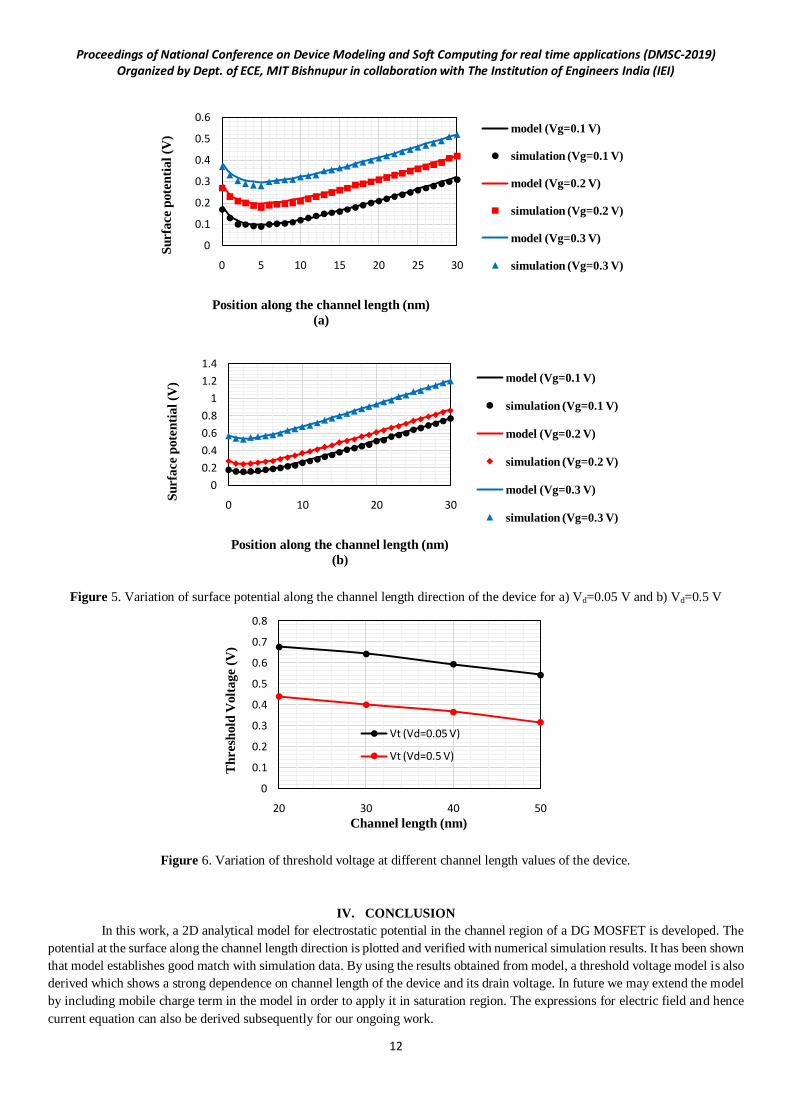
It is found from Fig. 5 that surface potential model for DG MOSFET is in good agreement with simulation result when Vg ranges
from 0.1 V to 0.3 V. As the model is valid in sub threshold region, we neglect mobile charges in our approach. Our model covers all
2D effects associated with source or drain side of the device. The variation of threshold voltage with respect to channel length is also
plotted in Fig. 6. It has been observed from Fig. 6 that threshold voltage increases as channel length decreases. Threshold voltage
decreases even further if drain voltage Vd is increased depicting the effect of DIBL. For such a shorter channel length device as
considered in our study, the increase of Vds has more influence on VT compared to a longer channel device as observed in Fig. 6.
Proceedings of National Conference on Device Modeling and Soft Computing for real time applications (DMSC-2019) Organized by Dept. of ECE, MIT Bishnupur in collaboration with The Institution of Engineers India (IEI)
12
Figure 5. Variation of surface potential along the channel length direction of the device for a) Vd=0.05 V and b) Vd=0.5 V
Figure 6. Variation of threshold voltage at different channel length values of the device.
IV. CONCLUSION
In this work, a 2D analytical model for electrostatic potential in the channel region of a DG MOSFET is developed. The
potential at the surface along the channel length direction is plotted and verified with numerical simulation results. It has been shown
that model establishes good match with simulation data. By using the results obtained from model, a threshold voltage model is also
derived which shows a strong dependence on channel length of the device and its drain voltage. In future we may extend the model
by including mobile charge term in the model in order to apply it in saturation region. The expressions for electric field and hence
current equation can also be derived subsequently for our ongoing work.
0
0.1
0.2
0.3
0.4
0.5
0.6
0 5 10 15 20 25 30
Su
rfa
ce p
ote
nti
al
(V)
Position along the channel length (nm)
(a)
model (Vg=0.1 V)
simulation (Vg=0.1 V)
model (Vg=0.2 V)
simulation (Vg=0.2 V)
model (Vg=0.3 V)
simulation (Vg=0.3 V)
0
0.2
0.4
0.6
0.8
1
1.2
1.4
0 10 20 30
Su
rfa
ce p
ote
nti
al
(V)
Position along the channel length (nm)
(b)
model (Vg=0.1 V)
simulation (Vg=0.1 V)
model (Vg=0.2 V)
simulation (Vg=0.2 V)
model (Vg=0.3 V)
simulation (Vg=0.3 V)
0
0.1
0.2
0.3
0.4
0.5
0.6
0.7
0.8
20 30 40 50
Th
resh
old
Volt
ag
e (
V)
Channel length (nm)
Vt (Vd=0.05 V)
Vt (Vd=0.5 V)

Proceedings of National Conference on Device Modeling and Soft Computing for real time applications (DMSC-2019) Organized by Dept. of ECE, MIT Bishnupur in collaboration with The Institution of Engineers India (IEI)
13
REFERENCES
[1] Arora N. MOSFET models for VLSI circuit simulation. Wien: Springe-Verlag;1993.
[2] Colinge J-P. FinFETs and other multi-gate transistors. Springer; 2007.
[3] Weber. Electromagnetic fields. 3rd ed. Wiley; 1950.
[4] Holtij T, Schwarz M, Kloes A, Iniguez B. 2D analytical modeling of the potentialwithin junctionless DG MOSFETs in
thesubthreshold regime. EuroSOI,Montpellier; 2012.
[5] Omura Y, Horiguchi S, Tabe M, Kishi K. Quantum-mechanical effects on thethreshold voltage of ultrathin-SOI nMOSFETs.
IEEE Electron Dev Lett1993;14(12):569–71. http://dx.doi.org/10.1109/55.260792.
[6] Kloes A, Kostka A. A new analytical method of solving 2D Poisson’s equation inMOS devices applied to threshold voltage
and subthreshold modeling. Solid-State Electron 1996;39(12):1761–75. http://dx.doi.org/10.1016/S0038-1101(96)00122-0.
[7] Schwarz M, Weidemann M, Kloes A, Iniguez B. 2D analytical calculation of theelectrostatic potential in lightly doped
Schottky barrier Double-Gate MOSFET.Solid-State Electron 2010;54(11).
[8] Holtij T, Schwarz M, Kloes A, Iniguez B. 2D analytical modeling of the potentialin doped multiple-gate-FETs including
inversion charge. Fringe Poster Sessionat ESSDERC/ESSCIRC, Helsinki; 2011.
[9] Holtij T, Schwarz M, Kloes A, Iniguez B. 2D analytical potential modeling ofjunctionless DG MOSFETs in subthreshold
region including proposal forcalculating the threshold voltage. ULIS2012, Grenoble; 2012.

Proceedings of National Conference on Device Modeling and Soft Computing for real time applications (DMSC-2019) Organized by Dept. of ECE, MIT Bishnupur in collaboration with The Institution of Engineers India (IEI)
14
STUDY OF THE PERFORMANCE OF DRIVING ASSISTANCE SYSTEM FOR COMPLEX TRIP
PLANNING OF ELECTRIC VEHICLES USING EVOLUTIONARY ALGORITHM
Mousumi Khanra (Karmakar)*1 and Arup Kr Nandi
2,3
1Dept. of Electronics & Communication Engineering, Mallabhum Institute of Technology, Bishnupur, India 2CSIR-Central Mechanical Engineering Research Institute, Durgapur, India 3Academy of Scientific and Innovative Research (AcSIR), Ghaziabad, India
Abstract: In order to tackle the various drawbacks of electric vehicle, a Driving Assistance System (DAS) was developed in the
recent past for properly manage the energy consumption through optimal driving during performing a trip. In the present paper, the DAS performance is analyzed towards planning a trip of typical configuration. Three driving cycles (neighborhood, urban and
highway) are considered for making various complexities of the trip for this investigation. The effect of driving cycle lengths in a
given trip on DAS results is demonstrated here. Moreover, effectiveness of DAS towards energy saving is analyzed for a typical
complex trip planning.
Keywords: Driving Assistance System, trip planning, electric vehicle, micro-trip, optimal driving strategy, trip complexity, multi-
objective optimization, driving cycle
I. INTRODUCTION
Day by day vehicular sectors are improving to increase the acceptance of Electric vehicles (EVs) for personal
transportation. To plan a trip using electric vehicle (EV) drivers need to carefully plan the trip in order to ensure that they will reach their destination. There are many factors that drive this important consideration such as limited battery storage, insufficient
charging stations, and high charging time when compared to conventional internal combustion vehicles. To overcome such EV
related drawbacks, an optimal driving based Energy Management System (so called DAEM) was introduced in [1]. The DAEM
system works based on multi-objective optimization problem (MOOP), MOOP of minimizing energy, E, minimizing trip time,
TTrip, and minimizing average jerk, JAvg were considered simultaneously. In [2], authors analyzed the influence of initial battery
charge and route characteristics on DAEM results. Depending upon the quality of road and other reasons (not overtaking zone,
hospital, school, high traffic, narrow road, bridge, etc.), the speed limits of a road are restricted [3] [4]. Such speed limit variations
create the trip complexity. In [5], the influence of trip complexity on DAEM results was investigated.
In the present paper, the performance of DAS and its working principle were studied by analyzing the its results in terms of the
battery state-of-charge after trip completion (SOCTrip_end) with total trip time (TTrip) in different complex trip planning [6-14].
Furthermore, an investigation on the amount of energy saving through adopting DAS during trip performing was carried out. In Section 2, the architecture of DAS and its working principle are briefly described and the definition of a micro-trip is presented
in Section 3. In section 4, results and discussion are presented. Finally, concluding remarks are stated in Section 6.
II. OPTIMAL DRIVING BASED DAS
Fig. 1 demonstrates the architecture of the optimal driving based energy management system (DAEM) [1] which comprises
two primary modules HMI (Human machine interface) and OTP optimal trip planning. HMI is used as a platform to collect
information from various sources (such as driver, GPS/Internet, etc.) and feed to OTP. Based on this information, OTP determines
a set of optimal driving strategies (multiple output information on trip planning). In addition, various other information
corresponding to the optimal driving strategies, namely range, trip end SOC and total trip time are also determined by OTP.
Determination of optimal driving strategies is made by solving a multi-objective optimization problem that considers three
conflicting objectives as follows.
kkavfT ipref refTTrip , ,,)( time tripofon Minimizati (1)
kkavfE ipref refB , ,,)( consumsionEnergy ofon Minimizati
(2)
k, ,kt, afJ i,...K,, pK
refJAvg Total1321
,...,2,1) (jerk average ofon Minimizati (3)
subject to
vvvdc
refdc
maxmin (4)
aaaK
ref max,...,2,1
min (5)

Proceedings of National Conference on Device Modeling and Soft Computing for real time applications (DMSC-2019) Organized by Dept. of ECE, MIT Bishnupur in collaboration with The Institution of Engineers India (IEI)
15
3.001.0 k p (6)
0.301.0 ki (7)
Where vref, aref and t are the reference velocity, acceleration/deceleration and corresponding durations [17], respectively, kp and ki
are the controller gains.
After each execution of OTP, a set of solutions (ODS) and corresponding various predicted information (such as range, trip end
SOC, and trip time) are presented to the driver for making a suitable trip planning [16]. Driver may choose an appropriate ODS
from the solution set based on the present circumstances or his desire. Otherwise, any decision making technique may be adopted to select a preferred one [15]. The driver is recommended to follow the preferred ODS for driving till the further ODS as
evaluated in the subsequent OTP execution. The subsequent execution of OTP is performed on the basis of current route data
corresponding to the original or updated trip start/end location (destination) and battery SOC.
Fig. 1. Schematic layout of DAEM architecture
III. CONCEPT OF MICRO-TRIP
A micro-trip may be defined as an excursion between two successive locations of travel route at which the vehicle is
definitely stopped [18] [19]. In general, an entire trip comprises several micro-trips. The length (range) of a micro-trip is defined
by the distance covered the two stop points of vehicle and may be called start and end points of that micro-trip, respectively. A
typical simple micro-trip consists of the following modes: acceleration mode, constant speed mode and deceleration mode.
Fig. 2. The velocity profile of a typical complex micro-trip
DC1 DC2 DC2 DC1
d1 d2 d4 d5
d
vstart=0
vref 1
vend=0
vref 2
vref 3
vref 2
vref 1
A B
DC3
d3

Proceedings of National Conference on Device Modeling and Soft Computing for real time applications (DMSC-2019) Organized by Dept. of ECE, MIT Bishnupur in collaboration with The Institution of Engineers India (IEI)
16
According to safety and differentiation of type of road, a micro-trip may face four category of road type based on maximum and
minimum speed limits [20] [21] such as neighborhood (speed range 8 km/h - 40 km/h), urban (speed range 40 km/h - 56 km/h), highway (speed range 56 km/h - 88.5 km/h), interstate (speed range 88.5 km/h - 112.6 km/h).
The minimum and maximum speed limits of each driving cycle need to be strictly followed by driver according to the rules and
regulation. Thus, the proposed DAS must be valid for each driving cycle. Accordingly, its performance for each driving cycle is
required to be studied independently for a complex trip planning using EV.
In real life journey, when we plan a trip at first we start the journey from a neighborhood driving zone and then after few
kilometers of journey reach to urban driving zone. Generally, after the completion of urban driving zone, we follow highway
driving zone. Before reach to final destination the trip again covers urban and neighborhood zones, respectively. In the present
paper, such type of trip is considered for DAS analysis shown in Fig. 2. In Fig. 2, d1 and d5 represents neighborhood driving cycle
(DC1), d2 and d4 represents urban driving cycle (DC2) and d3 represents highway driving cycle (DC3).
Fig. 2 demonstrates the velocity profile of a typical complex micro-trip that consists of three driving cycles with five parts. The
first and fifth part of the micro-trip corresponds to neighborhood driving cycle, the 2nd and 4th part corresponds to urban driving
cycle and 3rd part corresponds to highway driving cycle. The vehicle reference speeds, vref1, vref2 and vref3 belong to 1st, 2nd and 3rd part of the micro-trip. The 5th part of micro-trip, the vehicle reference speed is same as 1st part and 2nd part of micro-trip, the
vehicle reference speed is same as 4th part. According to the definition of micro-trip, vstart and vend in Fig. 2 both are zero.
According to rule of traffic signal, at each signal normally the vehicle has to stop at a red signal light until the signal becomes
green. Locations, A and B (in Fig. 2) are considered as two successive red signals.
IV. RESULTS AND DISCUSSION
Fig. 3 demonstrates the Pareto front of DAS results obtained through solving the MOOP using a non-dominated sorting
genetic algorithm (NSGA II) [22] for the typical complex micro-trip of length 20 km and 50 km. Optimization results obtained by
varying length of three driving cycles for the same MT (micro-trip) and analyzed the performance in order to understand the effect
of complexity due to the driving cycle length. The Fig. 3a and Fig. 3b shows the Pareto-optimal solutions of SOCTrip_end with TTrip for the complex micro-trips (as shown in Fig. 2) for different values of urban and highway driving cycle length. The total trip
length for both cases was considered as 20 km.
From Fig. 3a, it was found that the Pareto fronts are overlapping for different urban driving cycle length for 20 km trip length with
fixed length of highway driving cycle (10 km). With increasing the urban driving cycle length, the characteristics of SOCTrip_end
and TTrip is not significantly changed. In Fig. 3b, with increasing the highway driving cycle length for fixed urban driving cycle
length, the Pareto fronts are not overlapping. Moreover, it was found that the Pareto front width is stretched with increasing the
highway driving cycle length and also improves the value of SOCTrip_end. Similar observation studies for 50 km trip length for the
same complex micro-trip as shown in Fig. 4.
From Fig. 4a and Fig. 4b, it was observed that with the increase of total trip length, Pareto front are not overlapped for different
length of urban and highway driving length. Moreover, from Fig. 4a and Fig. 4b, it was noticed that the SOCTrip_end value is
increased with the increase of urban and highway driving cycle length for fixed trip length (50km). The rate of increase of
SOCTrip_end with respect to TTrip was found more when the highway driving cycle length is high (as shown in Fig. 4b). But when the urban driving cycle length is high, rate of SOC increase with respect to time is not so high (as shown in Fig. 4a) compare to
high highway driving cycle length for same micro-trip, as shown in Fig. 4(b). Therefore, from the plot of Pareto-optimal solutions
of SOCTrip_end with TTrip for the typical complex micro-trip, we see that with the increase of length of urban and highway driving
cycle energy consumption is reduced and finally at the end of trip we get high SOCTrip_end with the use of DAS. Moreover, the rate
of trip end SOCTrip_end improvement is higher in high length of highway driving cycle than urban driving cycle.
0.675
0.68
0.685
0.69
0.695
0.7
0.705
0.71
0.715
0.72
0.725
1000 1500 2000
U10_H10
U5_H10
0.675
0.68
0.685
0.69
0.695
0.7
0.705
0.71
0.715
0.72
1000 2000 3000
U10_H5
U10_H10

Proceedings of National Conference on Device Modeling and Soft Computing for real time applications (DMSC-2019) Organized by Dept. of ECE, MIT Bishnupur in collaboration with The Institution of Engineers India (IEI)
17
Fig. 3. Comparative results of a typical complex micro-trip (20 km trip length) with different lengths of urban and highway
driving cycle (a) Highway length=10 km (b) Urban length=10km
Fig. 4. Comparative results of a typical complex micro-trip (50 km trip length) with different lengths of urban and highway
driving cycle (a) Highway length=10 km (b) Urban length=10km
The effectiveness of DAS is analyzed by comparing the energy consumptions with and without using DAS during trip
performing. Table 1 presents the amount of energy saving can be obtained for different driving cycle lengths of the same micro-trip as presented in Fig. 2. Based on energy saving for different driving cycle length of a complex micro-trip are analyzed and
listed in Table 1.
Table 1: Energy saving for different driving length of a complex micro-trip with the use of DAS
Trip Length (Km)
Driving cycle Length (Km) Energy Consumption (J) Energy Saving
(%) Urban Highway With DAS Without DAS
20
5 10 739481 856610 13.6736
10 10 745500 858730 13.1858
10 5 785603 825032 4.77909
50
5 10 194051 205237 5.45028
10 10 191810 203070 5.54489
15 10 189754 200194 5.21494
10 5 193975 200412 3.21188
10 15 189092 204704 7.62662
From Table 1, it was observed that there is always energy saving with adopting DAS but is varies with the driving cycle length.
For a 20 km trip length, a maximum of 13.67% energy saving is found with 10 km highway length, 5 km urban length and
remaining is neighborhood. If we decrease the highway length from 10 km to 5 km, the energy saving is reduced from 13.18% to
4.779%. On the other hand, the speed limits of highway driving cycle are higher than urban or neighborhood. Thus, the above
finding indicates that selection of optimal speed in higher driving cycle is important.
On the other hand, variation of urban length, the energy saving (%) is not found to be significantly changed. Similar observation is
also noticed for other trip lengths, and it was noticed that energy saving increasing with increasing the highway driving cycle
length provided that the speed should be optimum.
0.45
0.46
0.47
0.48
0.49
0.5
0.51
0.52
3400 3900 4400
U5_H10
U10_H10
U15_H10
0.45
0.46
0.47
0.48
0.49
0.5
0.51
0.52
3000 4000 5000 6000
U10_H5
U10_H10
U10_H15

Proceedings of National Conference on Device Modeling and Soft Computing for real time applications (DMSC-2019) Organized by Dept. of ECE, MIT Bishnupur in collaboration with The Institution of Engineers India (IEI)
18
V. CONCLUSIONS
In this paper, the performance of DAS is analyzed for a typical complex trip planning. The above observations draws the following conclusions-
For low trip length, variation of urban driving length is not significantly changes the trip end SOCTrip_end rather variation
of highway driving length.
For high trip length, with the increase of urban and highway driving length trip end SOCTrip_end improved.
Percentage of energy saving is found in any trip length with the use of DAS in a complex trip planning.
Maximum energy saving is found in high value of highway length and minimum energy saving is found in low value of
highway length.
ACKNOWLEDGMENT
First author is thankful to Principal of Mallabhum Institute of Technology, Bankura, West Bengal, India to provide the
necessary support for her research work at CSIR-CMERI, Durgapur, India.
REFERENCES
[1] M. Karmakar, A.K. Nandi, “Trip Planning for Electric Vehicle through optimal driving using Genetic Algorithm,
International Conference on Power Electronics,” Intelligent Control and Energy Systems (IEEE ICPEICES ), Delhi, India , 2016.
[2] M. Karmakar, A.K. Nandi, “Driving Assistance for Energy Management in Electric Vehicle, International Conference on
Power Electronics,” Drives and Energy Systems (IEEE PEDES), Trivandrum, Kerala, India, 2016, .
[3] S. Tsugawa, Super smart vehicle system: Future intelligent driving and the measures for the materialization, in Proceeding of
Surface Transportation: Mobility, Technology, and Society. Proceedings of the IVHS AMERICA 1993 Annual
Meeting,Washington, D.C., pp. 192–198,1993.
[4] H. Fujii, O. Hayashi, N. Nakagata, Experimental research on intervehicle communication using infrared rays, in Proc. IEEE
Intelligent Vehicles Symposium, Tokyo, Japan, pp. 266–271, 1996.
[5] M. Khanra, A.K. Nandi, “Influence of trip complexity on optimal driving based Energy Management System of Electric
Vehicle”, International Conference on Communication and Electronics Systems (ICCES 2019), Coimbatore, India , 2019.
[6] Feng, L., Ge, S., Liu, H., Electric Vehicle Charging Station Planning Based on Weighted Voronoi Diagram. Proceedings of
Power and Energy Engineering Conference (APPEEC), Asia-Pacific, published by IEEE, pp. 1-5, 2012. [7] E. Gilman, A. Keskinarkaus, S. Tamminen, S. Pirttikangas, J. Röning, and J. Riekki, “Personalised assistance for fuel-
efficient driving,” Transportation Research Part C: Emerging Technologies, 58D, pp. 681-705, 2015.
[8] M. Ceraolo, G. Pede, Techniques for estimating the residual range of an electric vehicle. IEEE Transactions on Vehicular
Technology 50 (1) 109-115, 2001.
[9] E.J. Yao, M.Y. Wang, Y.Y. Song, T. Zuo, Estimating the cruising range of electric vehicle based on instantaneous speed and
acceleration, Applied Mechanics and Materials 361-363, 2104-2108, 2013.
[10] A. Szumanowski, Y. Chang, Battery management system based on battery nonlinear dynamics modeling, IEEE Transactions
on Vehicular Technology 57(3), 1425-1432, 2008.
[11] K.A. Smith, C.D. Rahn, C.Y. Wang, Model-based electrochemical estimation and constraint management for pulse operation
of lithium ion batteries, IEEE Transactions on Control Systems Technology 18(3), 654-663, 2010.
[12] W.X. Shen, K.T. Chau, C.C, Chan, E.W.C. Lo, Neural network-based residual capacity indicator for nickel-metal hydride batteries in electric vehicles, IEEE Transactions on Vehicular Technology 54(5), 1705-1712, 2005.
[13] F. Baronti, W. Zamboni, N. Femia, R. Saletti, M.Y. Chow, Parameter identification of Li-Po batteries in electric vehicles: A
comparative study. IEEE International Symposium on Industrial Electronics, Taipei, Taiwan, doi:10.1109/ISIE.2013.6563887
, pp. 1-7, 2013.
[14] L.L. Du, B. Li, H.D. Zhang, Estimation on state of charge of power battery based on the grey neural network model, Applied
Mechanics and Materials 427-429, 1158-1162, 2013.
[15] K. Miettinen, Nonlinear multiobjective optimization. Kluwer, Boston, 1999.
[16] A.K. Nandi, D. Chakraborty, and W. Vaz, “Design of a comfortable optimal driving strategy for electric vehicles using multi-
objective optimization,” Journal of Power Sources, vol. 283, pp. 1-18, 2015.
[17] W. Vaz, A.K. Nandi, U.O. Koylu, “A multi-objective approach to find optimal electric vehicle acceleration: simultaneous
minimization of acceleration duration and energy consumption,” IEEE Transactions on Vehicular Technology, (DOI
10.1109/TVT.2015.2497246), 2015. [18] Haan, M. Keller, Real-world driving cycles for emission measurement: ARTEMIS and Swiss cycles, Final Report, 2001.
[19] M. Andre, Real-world driving cycles for measuring cars pollutant emissions – Part A: The ARTEMIS European driving
cycles, Institut National de Recherche sur les Transports et leur Securite (INRETS), Report INRETS-LTE 0411, 2004.

Proceedings of National Conference on Device Modeling and Soft Computing for real time applications (DMSC-2019) Organized by Dept. of ECE, MIT Bishnupur in collaboration with The Institution of Engineers India (IEI)
19
[20] A. G. Ostensen , Effects of Raising and Lowering Speed Limits on Selected Roadway Sections, U.S. Department of
Transportation, Federal Highway Administration, Publication No. FHWA-RD-97-084, 1997. [21] M.I. Berry,The effects of driving style and vehicle performance on the real-world fuel consumption of US light-duty
vehicles. Master’s Thesis, Massachusetts Institute of Technology, available at http://web.mit.edu/sloan-auto-
lab/research/beforeh2/files/IreneBerry_Thesis_February2010.pdf, 2010.
[22] Deb, K., Pratap, A., Agarwal, S. and Meyarivan, T., A fast elitist non-dominated sorting genetic algorithm
for multi-objective optimisation: NSGA-II. IEEE Transactions on Evolutionary Computation 6 (2), 2002. .

Proceedings of National Conference on Device Modeling and Soft Computing for real time applications (DMSC-2019)
Organized by Dept. of ECE, MIT Bishnupur in collaboration with The Institution of Engineers India (IEI)
20
SOLVING TRAVELLING SALESMAN PROBLEM USING INTUITIONISTIC FUZZY SET BASED
GENETIC ALGORITHM
Amalendu Si* 1 and Sujit Das
2
1Dept. of CSE, Mallabhum Institute of Technology, Bishnupur-722122, India 2Dept. of Computer Science and Engineering, NIT Warangal, Warangal 506004, India
Abstract: The purpose of the travelling salesman problem is to find the optimal path for visiting all cities in each set of cities and
finally return to the stating city. Finding the optimal path is often critical due to the presence of some contradictory parameters.
In this article, we present an approach to solve travelling salesman problem (TSP) using intuitionistic fuzzy set (IFS) based
genetic algorithm (GA), where the travelling cost between cities is considered as benefits and expenditures which are represented
using IFSs. Total cost of the path is estimated using intuitionist fuzzy aggregation operator (IFAO). Then GA is used to reduce the
searching complexities and to find the optimal solution.
Keywords: Genetic Algorithm, Intuitionistic Fuzzy Sets, Intuitionistic Fuzzy Aggregation Operator, Travelling Salesman Problem.
I. INTRODUCTION
Travelling salesman problem (TSP) [2] is a well-known, popular and extensively studied problem in the field of conditional
optimization. The definition of TSP is that there are number of cities of which, the salesman start his journey from his home city
to visit all cities exactly once and then return to the home city again and find the order of the cities in such a way, so that the cost
of the tour is minimum. The cost is calculated on the basis of distance between cities, travelling time, security during travel, loss
of energy etc. The TSP is easy to describe but too difficult to solve. Initially, the TSP is solved by using the different mathematical
techniques like random searching, dynamic programming, branch and bound method, greedy procedure and so on, to reduce the
time complexity. Then the TSP is modified in various ways depending on the application type, varieties of purposes and
requirements of the users and current situations. After the modification of the TSP, the simple mathematical procedure is not
appropriate to get optimal or suitable solutions in the reasonable time. Then, many researchers have proposed different modified
methods to solve the problem. Among them, some researchers have changed the constraints of the problem and some researchers
have introduced new parameters which are directly related with problem. Author [4] has proposed a fuzzy multi-objective linear
programming problem solving technique and explored the aspiration parameter for choosing the route. Here, the decision
variables are defined with the three parameters which are related to travelling cost, time and distance. Then the three LP problems
are considered for the said parameters for the optimization and after that, based on those optimized solutions, the authors have
created another simple LP problem for calculating the aspiration level ‘L’ of the route. In this article, three LP problems have been
considered to optimize three parameters. An ‘n’ parameter problem is needed to solve an ‘n’ number of LP problems which is
time consuming. A new technique is introduced by S. Dhanasekar and others [3] to solve the TSP in fuzzy environment by
ranking the fuzzy numbers. A. Kumar and A. Gupta [7] have proposed two methods of fuzzy assignment problems and fuzzy
travelling salesman problems with LR parameters to solve the TSP easily. So, most of the researchers consider either maximizing
the cost of the tour or minimizing the loss. When an expert considers the maximization side then, the minimization side is in dark
position and alternatively when he considers the minimization side then maximization side in dark position. In this article, we
consider both the maximization and minimization side of the tour. Intuitionist Fuzzy Sets (IFS) is a suitable technique to represent
both of them within a single quantizer and Intuitionist Fuzzy Aggregation Operator (IFAO) is applied to merge them. Then we use
Genetic Algorithm (GA) to choose the best alternative among the available solutions.
II. CLASSICAL TSP AND SOLVING TECHNIQUE
The mathematical notation of the Travelling Salesman Problem can be represented with a graph, where a city is represented
with a point or node and the link between two nodes is called edge or arc. A distance is associated with each edge which is
considered as the cost of edge. The cost of the edge is fixed and static. If a node of the graph is connected with all other nodes of
the graph, it is called a complete graph. A round trip of all the cities corresponds to a special subset of the edges. When each city
is visited exactly once and returned to the staring city again, it is called a tour or Hamiltonian cycle (h) of the graph. The hi is the
combination of cityi, cityk1, cityk2,.... citykm, cityi, where k1, k2...km ϵ(n-i). The total cost (c) of the tour denotes round trip distance

Proceedings of National Conference on Device Modeling and Soft Computing for real time applications (DMSC-2019)
Organized by Dept. of ECE, MIT Bishnupur in collaboration with The Institution of Engineers India (IEI)
21
of the cycle. The cost of the Hamiltonian cycle hi is denoted as ci and calculated using (1). Then, among the Hamiltonian cycles,
the minimum cost (coptimal) cycle is chosen and considered as final or optimal solution. The TSP is symmetric or asymmetric,
depending on the direction of the edge. When the edges are bidirectional, then the problem becomes symmetric, otherwise the
problem is considered as an asymmetric problem. If the travelling cost from the cityi to cityj is denoted with cij if cij=cji then the
problem is symmetric. We introduce a variable xij of each arc with the value of either 0 or 1 for the representation of the problem.
When xij is 1 (i=1,2,3…n and j=1,2,3….n) it means that the arc is connected from cityi to cityj. Let xii=0 (i=1, 2, 3…n) which
means that no tour is considered from a city to itself.
1
1
n
i ik ki
k
c c c
(1)
minoptimal ii
c c (2)
III. INTUITONISTIC FUZZY SET
In this section, we briefly review about IFS, its operation and comparison.
Definition of IFS and IFV with necessary conditions
Atanassov [8] defined the concept of intuitionistic fuzzy sets in 1989. Consider a set E be a universal set. An intuitionistic fuzzy
sets or IFS in Z is an element having the form ' '' , ,
A AA z z z x Z where the function
': [0,1]
A Z and
' : [0,1]A Z denoted the degree of membership and the degree of non membership respectively of the element z from Z to
set A’. For any element zϵZ satisfy the condition ' ',0 1
A Az z z Z .
The function ' : [0,1]A Z specified by ' ' '( ) 1 ,
A A Az z z z Z defines the degree of uncertainty of
membership of the element z to set A` called hesitant function. For a fixed zϵ Z , an object ' ',
A Az z is usually called
intuitionistic fuzzy value (IFV) or intuitionist fuzzy number (IFN).
Basic Operation On Intuitionistic Fuzzy Sets
Addition and Multiplication of IFSs
The operation of addition and multiplication on intuitionistic fuzzy values are defined by Atanassov [8] as follows: Let
' '' ,
A AA z z and ' '
' ,B B
B z z be two IFVs, then
' ' ' ' ' '' ' ( . , . )
A B A B A BA B
(3)
' ' ' ' ' '' ' ( . , . )A B A B A BA B
(4)
These operations are constructed in such a way that they generate IFV, since it is proved that
' ' ' ' ' '0 . . 1A B A B A B and ' ' ' ' ' '
0 . . 1A B A B A B
.
Each ordinary fuzzy set A may be written as:
A`= ' ', ( ),1 ( )A Az z z z Z .
If ', 'A B IFSs , then the following operations can be found in
1) ' 'A B iff ' ' ' '&
A B A Bz z z z z Z ;
2) ' 'A B iff ' ' ' '&
A B A Bz z z z z Z ;
3) 'CA = ' ', , |A Az z z z Z .

Proceedings of National Conference on Device Modeling and Soft Computing for real time applications (DMSC-2019)
Organized by Dept. of ECE, MIT Bishnupur in collaboration with The Institution of Engineers India (IEI)
22
Multiplication of IFS with real values
The addition and multiplication of IFSs with real values are evaluated using (3) and (4) in [8].
' '' 1 1 ,n n
A AnA & ' '' ,1 1nn n
A AA , where n is any integer.
These aforementioned operations produce IFVs which depends not only for integer n but also for all real value 0 i.e.,
' '' 1 1 ,
A AA
(5)
' '' ,1 1
A AA
(6)
Intuitionistic weighted arithmetic mean: the IWAM can be found using expression (3) and (6) as follows:
2 2
1 1
..... 1 1 ,i
i
i i
n nw
w
i i n n A A
i i
IWAM w A w A w A
(7)
Where 0 ` 1iw and 1
` 1n
i
i
w
.
IFNs is determined using this aggregating operator which is the most accepted in the solution of MCDM problem in the
intuitionistic fuzzy setting.
Comparison of IFSs
The comparison of IFVs is important problem in this paper. The S z z z , where z is an IFV, is used as a score
function in Chen and Tan [3]. In addition to the above score function, the accuracy function as H z z z is
introduced in Hong and Choi [6]. In Xu [9], the function S and H is used to construct order relation between any combinations of
two intuitionistic fuzzy values (c` and d`) as follows:
If ( ' ( '))S c S d , then ' 'c d ;
( ' ( '))S c S d , then
(1) If ( ' ( '))H c H d then ' 'c d
(2) If ( ' ( '))H c H d , then ' 'c d
IV. GENETIC ALGORITHM
GAs [7] are very much practical methods of robust optimisation. The general idea is the replication of natural evolution in
the search for finding the most favourable solution of a given problem. In nature, individuals compete to survive in unfit
environment. In this competition, only the fittest individuals survive and reproduce the next generation. Therefore, the genes of
the fittest survive while the genes of weaker individuals die out. Genetic material is saved into the chromosomes. Parents’ genetic materials are mixed during reproduction and the offspring has genes of both parents. Also, an individual’s genetic material can be
transformed by crossover and mutation operations. Mutation operation can randomly change single or multiple instance of genes
of the chromosome and avoid local optimization. Whereas crossover operation rapidly changes the genes of chromosome
internally (intra) or with the interaction with other chromosome (inter) to improve the standard quality of the chromosome. When
we simulate the natural genetic algorithm, each individual (chromosome) represents a potential solution of a given problem. The
GA expends most of the time on evaluating population. Therefore, the representation of chromosome is very important; it could
be an array of bits, a number, an array of numbers, a matrix, a string of characters or any other data structure. A chromosome must
gratify given precision and constraints and of course, it must be suitable for the implementation of genetic operators. Fig. 1 shows
the common structure of GA.

Proceedings of National Conference on Device Modeling and Soft Computing for real time applications (DMSC-2019)
Organized by Dept. of ECE, MIT Bishnupur in collaboration with The Institution of Engineers India (IEI)
23
Algorithm: Genetic Algorithm
Begin
Generate population
Do
Begin
Evaluate population
Choose specific for succeeding population
Execute crossover and mutation
While upto set condition
End
End
Fig. 1 Pseudo Code of basic genetic algorithms
V. THE MODIFIED TSP AND REPRESENTATION IN IFS AND GA
There are several ways to represent the TSP for solving the problem using genetic algorithm. In this article, we use two
matrices for this purpose, one is called binary matrix, and another is cost matrix. The size of the matrices is nxn, where n denote
the number of cities considered in the problem. Binary matrix is used to indicate the links among the cities with the help of
elements xij, where xij=1, if there is a link between cityi to cityj, otherwise the value of xij is 0. The binary matrix is symmetric. The
cost matrix highlights the travelling cost between two cities with the help of cost element fij, where fij= (µij, νij) which is an
intuitionistic fuzzy number (IFN). IFN consists of two parameters, µij and νij where µij indicates the benefit criteria and νij
indicates the cost criteria of the link. The benefit criteria can reduce the travelling cost like shortest distance, high speed roadway,
consumption of low energy etc. whereas the cost criteria of the link can increase the travelling cost of the link like high traffic,
low security, high toll fees or service tax etc. between the cityi to cityj. The basic condition of the two variables µij and νij is that
0≤ µij+νij≤1 because the values of µij increase if the values of νij decrease or vice versa. The binary matric of the problem is
symmetric whereas the cost matrix of the same problem may not be symmetric as the value of µij and µji or νij and νji are not same.
Because the traffic of the road in all directions is not same; in forward direction of the road there may not be any traffic whereas in
the backward direction there may be heavy traffic. The values of parameter, µij and νij change from time to time or season to
season or occasion to occasion. The speed of vehicles depends on weather; the speed is affected during rainy and winter season
due to heavy rain and fog respectively. The links between the cities are classified into two types: symmetric link and asymmetric
link. For the symmetric link, the travelling cost fij between the cityi to cityj and travelling cost fji between the cityj to cityi are the
same; whereas in the asymmetric link the travelling cost fij between the cityi to cityj and travelling cost fji between the cityj to cityi
are not the same. The asymmetric links play an important role to create the optimal route because changing the direction of link
can increase the cost of the route.
At first, we generate the chromosomes for the implementation of GA in TSP problem. The chromosomes consist of a
sequence of integers. This sequence of integers indicates the sequence of nodes which are visited by the salesman to complete a
round trip tour. So, the number of genes of the chromosome depends on the number of nodes present in the problem. If the
problem holds ‘n’ number of nodes, the length of the chromosome of the problem is ‘n+1’. During the generation or after the
reproduction of the chromosome, it surely follows the binary matrix. According to the constrains of the TSP problem, the
chromosome must hold all the genes with single instance and the sequence of the genes of the chromosome depends on the link
between the nodes of the problem that is presented in binary matrix. If the chromosome holds multiple instances of genes or if any
gene remains absent in the chromosome and if there’s no link between the two nodes based on genes sequence within the
chromosome, then the chromosome will be defective. If the chromosome is correct, we process it further otherwise discard.
According to Fig 3, we consider the chromosome [1,6,2,3,4,7,5,8,9,1] as defective because this chromosome represents the tour 1-
6-2-3-4-7-5-8-9-1. This tour is discontinuous due to the absence of the link between the nodes 4 and 7. We consider another
chromosome [1,9,7,8,5,4,3,2,6,1] of the same figure which represents the route 1-9-7-8-5-4-3-2-6-1. This route visits all the nodes
at one time which are present in the problem and the tour ends at the starting point. If the links between the nodes of the tour are
present in the defined binary matrix of the problem, the chromosome is correct. After generating the correct chromosome, we
calculate the fitness value of the chromosome. The fitness value indicates the travelling cost of the round-trip tour. Each link has a
travelling cost in the form of IFN. A tour consists of a number of IFN. The IFAO operator is used to merge all the IFNs of the
tour. The resultant IFN is considered as the travelling cost of the tour.
Correct chromosomes [1,9,7,8,5,4,3,2,6,1], [1,6,2,3,4,5,8,7,9,1], [1,6,2,3,4,5,7,8,9,1].

Proceedings of National Conference on Device Modeling and Soft Computing for real time applications (DMSC-2019)
Organized by Dept. of ECE, MIT Bishnupur in collaboration with The Institution of Engineers India (IEI)
24
Defective chromosomes [1,6,2,3,4,7,5,8,9,1], [1,6,2,3,4,6,7,5,8,9,1], [1,2,3,4,5,6,7,8,9,1].
The correct chromosomes are considered as initial solutions. Then, we apply GA based crossover and mutation operators to
modify the initial chromosome and create the new chromosome which is better than the parent chromosome by decreasing the
travelling cost of the tour.
Here we use the reverse crossover operation for avoiding premature convergence and rapid change. We use the exchange mutation
operation for randomly choosing and exchanging the genes of the chromosome to explore the search space. Both the mutation and
crossover operations play an important role to converge the optimal or acceptable solution.
In reverse crossover [7] operation, we randomly choose a set of sequence cities in the tour and arrange them in reverse order. Let’s
consider the tour [1,9,7,8,5,4,3,2,6,1] and Choose the sequence of cities (4,3,2,6) and arrange them in reverse order like (6,2,3,4)
so the resultant tour after the crossover operation is [1,9,7,8,5,6,2,3,4,1].
Exchange mutation [8] operation was projected by Banzhaf in 1990. In the exchange mutation operation, we haphazardly choose
two cities from the tour and replace them. If we think the tour represented by [1, 3, 4, 5, 2, 1] and choose the city3 and city2 and
exchange them, then the resultant chromosome will be [1, 2, 4, 5, 3, 1].
VI. PROPOSED ALGORITHM
Fig.2 explains the extended version of GA. We consider P(c) and C(c) as the parent and child in current generation c
respectively. Fitness value FP(c) and FC(c) of parent and child is computed by the IFAO operator correspondingly. We choose the
next generation P(c1) from P(c) and C(c) according to their fitness values. The general representation of GA is described as
follows:
Algorithm: Evolution of Genetic Algorithm
Input: data sets of the problem, GA constrains
Output: Optimal solution
Begin
Initialize population P(c)by encoding
If P(c)is defective
Discard and reinitialize P(c)
Do
Begin
Evaluate P(c) by decoding
Calculate fitness value FP(c)of P(c)using IFAO operator
Create C(c)from P(c)by reverse crossover and exchange mutation
If C(c)is defective
Discard and regenerate C(c)
Evaluate C(c) by decoding
Calculate fitness value FC(c) of C(c) using IFAO operator
Select P(c1)from P(c)and C(c)base of minimum value of FP(c)and FC(c)
P(c) = P(c1)
While (FP(c) ≠ FC(c))
End
End
Fig. 2 Pseudo Code of modified genetic algorithms
VII. CASE STUDY
We consider the following asymmetric travelling salesman problem with nine cities and connection among those cities is
shown in fig.3. The connectivity and cost of the connection are represented with the help of binary matrix and cost matrix
respectively. The salesmen start the journey from his home city and visit all the cities exactly once and finally return to the home
city again by the minimum travelling cost of the tour. Here, the travelling cost between two cities is represented by the fuzzy
quantifier which highlights the cost or profit and loss or expenditure in the form of IFN. This problem is solved by our proposed
method.
Initially, the generated chromosome with route map is 1-2-6-3-4-5-7-8-9-1. The travelling cost from city to city of the route is
(1.0, 0.0), (0.2, 0.75), (0.3, 0.6), (0.7, 0.25), (0.3, 0.65), (0.5, 0.5), (0.6, 0.25), (0.8, 0.1) and (0.2, 0.8) respectively according to the
sequence. Then, the total calculated travelling cost with the help of eq. (7) is (0.46, 0.57). After that, the created route will be

Proceedings of National Conference on Device Modeling and Soft Computing for real time applications (DMSC-2019)
Organized by Dept. of ECE, MIT Bishnupur in collaboration with The Institution of Engineers India (IEI)
25
modified iteratively and finally get the tentative optimal route map, 1-9-7-8-5-4-6-3-2-1 in which the travelling cost is (0.75,
0.12).
Fig 3 (a). A graph representation of a network of cities.
1 0 0 0 1 0 0 1
1 1 0 0 1 0 0 0
0 1 1 0 1 0 0 0
0 0 1 1 1 0 0 0
0 0 0 1 0 1 1 0
1 1 1 1 0 1 0 1
0 0 0 0 1 1 1 1
0 0 0 0 1 0 1 1
1 0 0 0 0 0 1 1
Fig. 3 (b) Binary Matrix of the Fig: 3
(1.0,0.0) (0.0,0.0) (0.0,0.0) (0.0,0.0) (0.5,0.5) (0.0,0.0) (0.0,0.0) (0.8,0.2)
(0.8,0.1) (0.5,0.2) (0.0,0.0) (0.0,0.0) (0.65,0.25) (0.0,0.0) (0.0,0.0) (0.0,0.0)
(0.0,0.0) (0.6,0.3) (0.7,0.25) (0.0,0.0) (0.35,0.55) (0.
0,0.0) (0.0,0.0) (0.0,0.0)
(0.0,0.0) (0.0,0.0) (0.65,0.2) (0.3,0.65) (0.8,0.1) (0.0,0.0) (0.0,0.0) (0.0,0.0)
(0.0,0.0) (0.0,0.0) (0.0,0.0) (0.3,0.65) (0.0,0.0) (0.5,0.5) (0.6,0.4) (0.0,0.0)
(0.4,0.6) (0.2,0.75) (0.3,0.6
) (0.8,0.1) (0.0,0.0) (0.6,0.3) (0.0,0.0) (0.7,0.1)
(0.0,0.0) (0.0,0.0) (0.0,0.0) (0.0,0.0) (0.65,0.25) (0.5,0.5) (0.8,0.1) (0.0,1.0)
(0.0,0.0) (0.0,0.0) (0.0,0.0) (0.0,0.0) (0.7,0.2) (0.0,0.0) (0.6,0.25) (0.9,0.1)
(0.2
, 0.8) (0.0,0.0) (0.0,0.0) (0.0,0.0) (0.0,0.0) (0.6,0.3) (0.5,0.5) (0.8,0.2)
Fig. 3 (c) Cost matrix of Fig. 3

Proceedings of National Conference on Device Modeling and Soft Computing for real time applications (DMSC-2019)
Organized by Dept. of ECE, MIT Bishnupur in collaboration with The Institution of Engineers India (IEI)
26
VIII. CONCLUSION
In this article, we solve the TSP with the help of GA in intuitionistic fuzzy environment. This hybrid implementing
technique handles both the uncertainty and ambiguity related to the problem and also manages profit as well as loss of the tour.
This is different from the other conventional TSP solving methods. Random searching of GA can reduce the time complexity of
the problem which is efficient from the traditional searching method. This is very important for the large size of chromosome and
high density connectivity of the problem. Generation of the correct chromosome and maintaining the correctness of the
chromosome after reproduction are considered as significant concerns in the proposed approach. Future scope of this research
work can be enhanced by considering the robustness nature of GA.
REFERENCES
[1] J. Botzheim, P. Foldesi, L. T. Koczy: Solution for Fuzzy Road Transport Traveling Salesman Problem Using Eugenic Bacterial Memetic Algorithm, IFSA-EUSFLAT 2009.
[2] A. Kumar, A. Gupta: Assignment and Travelling Salesman Problems with Coefficients as LR Fuzzy Parameters,
International Journal of Applied Science and Engineering, 10, 3: 155-170.2012.
[3] S. Dhanasekar, S. Hariharan, P. Sekar: Classical Travelling Salesman Problem (TSP) based Approach to Solve Fuzzy TSP using Yager’s Ranking, International Journal of Computer Applications (0975 – 8887) Volume 74– No.13, July 2013.
[4] S. Fereidouni: Solving traveling salesman problem by using a fuzzy multi-objective linear programming, African Journal of
Mathematics and Computer Science Research Vol. 4(11), pp. 339-349, October 2011.
[5] B. Hu, G. R. Raidl: Solving the Railway Traveling Salesman Problem via a Transformation into the Classical Traveling
Salesman Problem. https://www.ac.tuwien.ac.at/files/pub/hu-08a.pdf
[6] D. H. Hong, C. H. Choi: Multicriteria fuzzy decision making problems based on vague set theory. Fuzzy Sets and Systems, 114, 2000, 103–113.
[7] P. Larranaga, C.M.H. Kuijpers, R.H. Murga, I. Inza, S. Dizdarevic: Genetic Algorithms for the Travelling Salesman
Problem: A Review of Representations and Operators, Artificial Intelligence Review 13: 129–170, 1999.
[8] K.T. Atanassov, C. Georgiev: Intuitionistic fuzzy prolog, Fuzzy Sets and Systems, 53, 1993, 121-128.
[9] Z.S. Xu, J. Chen, J.J. Wu: Clustering algorithm for intuitionistic fuzzy sets, Information Sciences, 178, 2008, 3775-3790.

Proceedings of National Conference on Device Modeling and Soft Computing for real time applications (DMSC-2019) Organized by Dept. of ECE, MIT Bishnupur in collaboration with The Institution of Engineers India (IEI)
27
MODELING AND SIMULATION OF A LOW-PROFILE MICROSTRIP PATCH ANTENNA OPERATING
AT 2.45 GHZ
Ankan Bhattacharya*
Dept. of Electronics and Communication Engineering, Mallabhum Institute of Technology, Bishnupur, India
Abstract: This paper focuses on modeling and simulation of a compact microstrip patch antenna. The dimensions of the antenna
are optimized to operate at 2.45 GHz frequency range. The antenna is 27.72 x 27.72 x 1.8 mm3 in dimension. Rogers TMM 4,
having an electrical permittivity of 4.5 is used as the substrate material. The Return Loss |S11| is ≥ 30 dB at 2.45 GHz. The
antenna shows a realized gain of 6.28 dB and directivity of 6.5 dBi at the resonant frequency.
Keywords: Microstrip Patch Antenna, Resonant Frequency, Return Loss, Gain, Directivity
I. INTRODUCTION
Introduction of microstrip patch antennas was a revolutionary step in the evolution of wireless communication technology.
This technology was described in detail by Carver and Mink in 1981 [1]. It is an integral part of any communicating device and is
used for transmission and reception of microwave signals. It can be of shapes and sizes e.g. rectangular, triangular, circular etc. [2-
4]. Various other theories related to design techniques is presented in [5] by Chang. In this paper, a simple square patch antenna
operating at 2.45 GHz frequency band is modeled and simulated in electromagnetic simulation software and the results are
presented.
II. ANTENNA DESIGN
The proposed antenna has a compact dimension of 55.45 x 55.45 mm2. The patch is placed on the top of the substrate. The
size of the patch is 27.73 x 27.73 mm2. The ground plane lies below the substrate. The patch is feed by a discrete port as shown in
Fig. 1. FR-4 having an electrical permittivity of 4.4 has been used as the substrate material. The substrate lies between the patch
and the ground plane. The dimensions of the antenna are obtained using the analytical formulae provided in [6].
Considering the resonant frequency, 𝑓𝑟 the effective length is given as,
𝐿𝑒𝑓𝑓 =𝑐
2𝑓𝑟 𝜀𝑒𝑓𝑓 (1)
The resonant freq. of TM mode of rectangular patch is given as,
𝑓𝑟 =𝑐
2 𝜀𝑒𝑓𝑓
𝑚
𝐿
2
+𝑛
𝑊
2 1/2
(2)
where, n and m are modes along the width W and length L respectively.
The patch’s width, W is now given as,
𝑊 =𝑐
2𝑓𝑟 𝜀𝑟+1
2
(3)
where, c denotes light wave’s velocity.

Proceedings of National Conference on Device Modeling and Soft Computing for real time applications (DMSC-2019) Organized by Dept. of ECE, MIT Bishnupur in collaboration with The Institution of Engineers India (IEI)
28
Fig. 1. Proposed microstrip patch antenna.
III. ANALYSIS OF ANTENNA RESPONSES
Fig. 2 shows the S11 vs. Frequency plot of the proposed patch antenna. The resonant frequency is exactly centered at 2.45
GHz. The return loss obtained i.e. |S11| ≥ 33 dB. The VSWR is ≤ 2 at 2.45 GHz as is observed from Fig. 3.
2.0 2.1 2.2 2.3 2.4 2.5 2.6 2.7 2.8 2.9 3.0
-40
-35
-30
-25
-20
-15
-10
-5
0
S1
1 (
dB
)
Frequency (GHz)
Fig. 2. Return Loss of proposed patch antenna.

Proceedings of National Conference on Device Modeling and Soft Computing for real time applications (DMSC-2019) Organized by Dept. of ECE, MIT Bishnupur in collaboration with The Institution of Engineers India (IEI)
29
2.0 2.1 2.2 2.3 2.4 2.5 2.6 2.7 2.8 2.9 3.0
0
1
2
3
4
5
6
7
8
9
10
VS
WR
Frequency (GHz)
Fig. 3. VSWR of proposed patch antenna.
The 3D radiation pattern of the proposed antenna is shown in Fig. 4. As observed from the scale, the antenna has achieved a
peak gain of 6.28 dB.
Fig. 4. 3D radiation pattern of the proposed antenna.
IV. CONCLUSION
A simple, discrete port fed, square shaped microstrip patch antenna has been modeled and simulated in this paper. The
antenna resonates exactly at 2.45 GHz. It has achieved a realized gain of 6.28 dB and directivity of 6.5 dBi. The antenna VSWR is

Proceedings of National Conference on Device Modeling and Soft Computing for real time applications (DMSC-2019) Organized by Dept. of ECE, MIT Bishnupur in collaboration with The Institution of Engineers India (IEI)
30
less than 2 at the resonant frequency. The planar design makes it suitable to be incorporated in devices supporting wireless
communications.
REFERENCES
[1] K. Carver and J. Mink, "Microstrip antenna technology," in IEEE Transactions on Antennas and Propagation, vol. 29, no.
1, pp. 2-24, January 1981.
[2] C. Krowne, "Cylindrical-rectangular microstrip antenna," in IEEE Transactions on Antennas and Propagation, vol. 31,
no. 1, pp. 194-199, January 1983.
[3] E. Kuester and D. Chang, "A geometrical theory for the resonant frequencies and Q-factors of some triangular microstrip
patch antennas," in IEEE Transactions on Antennas and Propagation, vol. 31, no. 1, pp. 27-34, January 1983.
[4] C. Wood, "Analysis of microstrip circular patch antennas," in IEE Proceedings H - Microwaves, Optics and Antennas,
vol. 128, no. 2, pp. 69-76, April 1981.
[5] D. Chang, "Analytical theory of an unloaded rectangular microstrip patch," in IEEE Transactions on Antennas and
Propagation, vol. 29, no. 1, pp. 54-62, January 1981.
[6] David M. Pozar; Daniel H. Schaubert, "Basic Microstrip Antenna Elements and Feeding Techniques," in Microstrip
Antennas: The Analysis and Design of Microstrip Antennas and Arrays , pp. 57-104, IEEE, 1995.

Proceedings of National Conference on Device Modeling and Soft Computing for real time applications (DMSC-2019) Organized by Dept. of ECE, MIT Bishnupur in collaboration with The Institution of Engineers India (IEI)
31
MODELING AND OPTIMIZATION OF A CMPA USING GENETIC ALGORITHM
Arnab De*1, Bappadittya Roy
2, Ankan Bhattacharya
3 and Anup K. Bhattacharjee
1
1Dept. of Electronics and Communication Engineering, National Institute of Technology, Durgapur, India 2Dept. of Electronics and Communication Engineering, Madanapalle Institute of Technology & Science, Madanapalle, India
3Dept. of Electronics and Communication Engineering, Mallabhum Institute of Technology, Bishnupur, India
Abstract: In this paper we have modeled a compact multiband patch antenna for wireless communications. Genetic Algorithm
(GA) has been applied for optimization of the antenna dimensions. Three antennas have been designed and simulated in IE3D
Software and the parametric dimensions of the proposed antenna have been optimized using GA for supporting multiband
operation.
Keywords: Microstrip Patch Antenna, Multiband operation, Genetic Algorithm
I. INTRODUCTION
Compared to conventional antennas, microstrip patch antennas have many advantages. The main advantages are (i) They are
having very less weight and possess a planar architecture (ii) They conform to the host surface (iii) Printed-circuit technology is used for mass production at low cost (iv) They can be easily integrated with other components (v) They support both Linear Pol. and Circular Pol. (vi) They are applicable for personal wireless communications (vi) They allow multiband frequency operations. Microstrip patch antennas have huge popularity due to their compact nature and planar architecture. They are useful for all portable wireless devices like all modern wireless gadgets. They are even used for satellite and TTCM operations. Several multiband/wideband antennas have been studied in [1-10], but there exists an issue regarding compactness in every case. In this paper we have presented a compact, multiband patch antenna for wireless communications. Genetic Algorithm (GA) has been applied for optimization of the antenna dimensions.
II. GENETIC ALGORITHM
Genetic Algorithm or popularly GA has been extremely popular in optimization of designs. The optimization process is based
on the popular concept of „Natural Selection‟ and „Survival of the Fittest‟. „Gene‟ is the unit of a Chromosome. In the process of
optimization the Genes are treated as Parameters and the fittest or in other words an optimum dimension of a parameter is selected
to obtain the „fittest‟ or the „best result‟ from the parameters provided [11].
III. ANTENNA DESIGN
The antenna evolution process is shown in Figs. 1, 2 and 3 respectively. In the first step, antenna 1 is considered as a reference
antenna, which consists of a simple rectangular patch and a ground plane. The reference patch has an width of „W‟ = 26 mm and length of „L‟ =18 mm . The ground plane has a width of W and length of L. The patch size contributes to the obtained resonant frequency while the ground size gives the overall gain and the frequency of operation of the reference antenna. In antenna 1, the gap between patch and ground plane is taken as w1 and l with measurements of 4.4322 mm and 5.614 mm respectively. This gap ensures the obtained results from the reference antenna. In the second step, a geometrical semi-circular elongated U shaped structure is used as a slot on the patch in antenna 2, the width and length of the patch and ground plane is also modified to get the resonant frequency at 56.2 & 7.8 GHz with a return loss of -16dB. The practice of using slot on the patch is a common method to reduce the patch size and thereby make the antenna resonate at desired frequencies by determining the radiation distribution pattern. The main advantage of slotted antenna lies in the fact of its design simplicity, robustness and using it in PCB board. Here, the bandwidth of the structure is better than the reference antenna 1 with an increase. The gap between the patch and ground plane is different on the sides. The gap w1 and l is considered as 4.432 mm and 5.614 mm respectively. In the proposed model i.e. in antenna 3, two geometrical elongated U shaped structures are used as slots on the patch. The proposed antenna (Antenna 3) is nested on FR- 4 substrate having dielectric constant Ɛr = 4.4 and loss tangent, δ=0.02 with a substrate height of 1.6 mm. The length and width of the model is well chosen as W=8.6000 mm and L=6.5503 mm.

Proceedings of National Conference on Device Modeling and Soft Computing for real time applications (DMSC-2019)
Organized by Dept. of ECE, MIT Bishnupur in collaboration with The Institution of Engineers India (IEI)
33
Fig. 1. Patch antenna (Antenna 1).
Fig. 2. Etched antenna (Antenna 2).
Fig. 3. Dual etched antenna (Antenna 3).
The patch has the U-shaped slots in the middle and so its width would be calculated as Wpatch = „w3+d+w4‟. The radius of U-shaped slot is chosen to be r =0.6703 mm. The depth or length of the U-shaped structure is optimized through multiple simulations and finally chosen as lslot = 1.1874 mm. One of the important parameter in this proposed model is the gap „g‟ between the two slots. This gap g = 2.4315 mm. The other parameters such as w1, w2, w3, w4, wgap, lgap can be seen from the table of parameters. All the parameters are collectively optimized (one at a time) to get the desired result. The feeding point of the antenna is chosen to be at the middle of gap „g‟. The feeding technique here is coaxial feed.. The dimensions of Antenna 3 i.e. proposed antenna were optimized using Genetic Algorithm (GA). The optimized dimensions of Antenna 3 are W = 25.32 mm, L = 17.84 mm, wgap = 7.75 mm, lgap = 5.25 mm, w1 = w2 = w3 = w4 = 5.75 mm, d = 6.25 mm, r = 3 mm and g = 4.25 mm. Another advantage of this type of feed is that it eliminates the feed radiation because it is directly connected to the patch. In the proposed model, the feed point is experimented at different locations and finally chosen at the aforementioned point in order to match the resonant frequency. Difficulty in fabricating can be counted as a disadvantage for this kind of feeding. The diameter and depth of the slot affects the resonant frequency and the gap between the patch and the ground affects the impedance bandwidth of the proposed model of antenna.

Proceedings of National Conference on Device Modeling and Soft Computing for real time applications (DMSC-2019)
Organized by Dept. of ECE, MIT Bishnupur in collaboration with The Institution of Engineers India (IEI)
34
IV. RESULTS AND DISCUSSION
Three antennas have been modeled in IE3D Software and simulated. Antenna 1 exhibits two resonant frequency bands (Fig. 4).
In Antenna 2 the resonating bands are shifted (Fig. 5). The resonating bands of the final antenna i.e. Antenna 3 are obtained at (5.15-5.25) GHz and (7.22-7.3) GHz respectively (Fig. 6). Fig. 7 shows the comparison plot of return losses of Antenna 1, 2 and 3.
Fig. 4. Return loss of Antenna 1.
Fig. 5. Return loss of Antenna 2.
Fig. 6. Return loss of Antenna 3.
Proceedings of National Conference on Device Modeling and Soft Computing for real time applications (DMSC-2019)
Organized by Dept. of ECE, MIT Bishnupur in collaboration with The Institution of Engineers India (IEI)
35
Fig. 7. Return losses of Antenna 1,2 and 3.
It can be clearly be observed that after optimization, the return loss of Antenna 3 has improved, which is ≥ 24 dB at around 4 GHz. An average gain ~ 3 dBi has been realized at the frequency bands of interest (Fig. 8).
Fig. 8. Realized gain of Antenna 3.
V. CONCLUSION
The receiving wire has a U space fix settled inside a rectangular ground plane opening alongside a coaxial feed. The proposed receiving wire additionally great reradiated over a wide range. For accomplishing better execution and to expand the increase of the receiving wire two U spaces are utilized both side of the reradiating patch. Further streamlining of the thickness of the substrate and other parameter of the proposed radio wire recurrence may add to more extensive transfer speed and increase likewise control the bordering impact of the receiving wire. The receiving wire will be appropriate for remote broadband, therapeutic imaging, radar applications, and other convenient remote applications.
REFERENCES
[1] Girish Kumar and K. P. Ray, Broadband Microstrip Antennas, Revised edition, Artech House, 2003. [2] Tapan Mandal and Santanu Das, “Microstrip feed Spanner Shape Monopole Antennas for Ultra Wide Band Applications”,
Journal of Microwaves, Optoelectronics and Electromagnetic Applications, Vol. 12, No. 1, June 2013. [3] Abdo Abdel Monem Shaalan and M. I. Ramadan, “Design of a Compact Hexagonal Monopole Antenna for Ultra-Wideband
Applications”, J Infrared Milli Terahz Waves, vol. 31, pp. 958–968, 2010. [4] K.P.Roy and S.Tiwari, “Ultra Wide Band Printed Hexagonal Monopole Antennas” IET Microwaves, Antenna and
Propagation, vol. 4, Iss. 4, pp. 437-445, 2010. [5] C. Zhang and A. E. Fathy, “Development of an Ultra – Wide Band Elliptical Disk Planar Monopole Antennas with Improved
Omni-directional Performance using a Modified Ground”, IEEE Int. Antenna Propagation Symp Dig., Alburqueque, NM. pp. 1689 – 1692, 2006.
[6] Z. N. Chen, T.SP. See, and X. M. Qing, “Small Printed Ultra Wide Band with Reduced Ground Plane Effect,”IEEE Trans. Antenna Propag., vol. 55, no.2, pp.383-388, Feb.2007.
[7] Hosseini, S. A., Z. Atlasbaf, and K. Forooraghi, “Two New Loaded Compact Planar Ultra-Wideband Antennas Using Defected Ground Structures”, Progress In Electromagnetic Research B, Vol. 2, 165–176, 2008.
[8] T.Yang and W. A. Davis, "Planar half-disk antenna structures for ultrawideband communications," in Proc. IEEE Int. Symp. Antennas Propagation, Jun. 2004, vol. 3, pp. 2508-2511.
[9] D. H. Kwon and Y. Kim, "CPW-fed planar ultrawideband antenna with hexagonal radiating elements," in Proc. IEEE Int. Symp. Antennas Propagation, Jun. 2004, voL 3, pp. 2947-2950.
[10] Hosseini, S. A., Z. Atlasbaf, and K. Forooraghi, “Two New Loaded Compact Planar Ultra-Wideband Antennas Using Defected Ground Structures”, Progress In Electromagnetic Research B, Vol. 2, 165–176, 2008.
[11] Srinivas, M. And Patnaik, L. M., 1994. Genetic algorithms: a survey, in Computer, vol. 27, no. 6, pp. 17-26.

Proceedings of National Conference on Device Modeling and Soft Computing for real time applications (DMSC-2019)
Organized by Dept. of ECE, MIT Bishnupur in collaboration with The Institution of Engineers India (IEI)
36
MODELING AND TESTING OF A PRINTED MONOPOLE ANTENNA FOR VARIOUS WIRELESS
APPLICATIONS
Susmita Bala*1, Partha Pratim Sarkar
2, Sushanta Sarkar
3 and Rajendra Prosad Ghosh
4 1Dept. of Electronics, Vidyasagar University, Midnapore, India,
2Dept. of USIC, University of Kalyani, Kalyani, India 3Dept. of USIC, University of Kalyani, Kalyani, India
4Dept. of Electronics, Vidyasagar University, Midnapore, India
Abstract: A monopole antenna with E shaped radiating patch is designed for multiband operations. Initially a simple E shaped
patch with partial ground plane of dimension 23mm×35mm is designed. This provides only one resonant frequency at 7.84 GHz.
Introducing a thin metallic strip in the ground plane, two additional resonances occur at 6.78 GHz and 9.22 GHz with the
previous resonance. The proposed antenna is fabricated using low cost FR4 substrate of dimension 42 mm×35mm×1.6mm. The
antenna offers gain of 4 dBi, 2 dBi and 3 dBi at three resonant frequencies of 6.78 GHz, 7.84 GHz and 9.22 GHz respectively.
Keywords: E-shaped antenna, multiband operation, wireless applications
I. INTRODUCTION
With the rapid development of the wireless communication systems, the role of antennas with multiband operations has
greatly increased because of combining numerous communication tasks in a single compact wireless system. To satisfy multiband
operation, these types of antennas should have important features like simple in structure, compact in size, easy of fabrication and
easily integrated with electronic circuits [1]. Among the different types antennas, the planar monopole antenna is a suitable
candidate for wireless application. They provide attractive features like low profile, light weight, low cost, multi resonance
behavior [2]. Numerous printed monopole antennas have been reported so far for multiband application. This multiband properties
has been achieved by using different shapes like meandered T [3] , dual U [4], symmetrical L and U [5], G shaped[6] of
monopole antennas. Previously reported different CPW fed monopole antenna [8-13] provides multiband characteristics. Different
slot antennas [13-16] are proposed to provide multiband nature. But these all reported antennas are complex in design. In this paper, a novel E shaped triband printed monopole antenna is proposed that provides triple resonant frequencies at 6.78
GHz, 7.84 GHz and 9.22 GHz which covers C band (4-8) GHz and X band (8-12) GHz wireless application. The antenna is
simple in design and compact.
II. PROPOSED ANTENNA DESIGN
The detailed geometry of proposed E shaped printed monopole antenna is shown in Fig.1. The antenna is printed on FR4
substrate with relative permittivity of 4.4, thickness 1.6 mm and loss tangent .02. Overall dimension of the proposed antenna is
42mm×35mm×1.6mm. The proposed E shaped patch consists of three rectangular metallic strips each of dimension 18×3.06mm
spaced 5.06mm apart is shown in Fig.1a (Top View). The E shaped patch is excited by 50Ω microstrip line of dimension 21.5 mm×3.06 mm. The bottom surface of the proposed antenna as shown in Fig.1b (Bottom View) consists of a partial ground plane
of dimension 35mm×25mm with a thin metallic strip of dimension 20mm×3.06mm. The antenna is designed and simulated by
Ansoft Simulation Software High Frequency Structure Simulator [17]. The optimal dimension of the proposed antenna is given in
Table 1.The fabricated antenna is shown in Fig.2.
Table1: Antenna dimensions
W W1 W2 W3 W4 Wg L L1 L2
35mm 14.94mm 0.5 mm 3.06mm 20.28 mm 3.06 mm 42 mm 3.06 mm 5.06 mm
L3 Lg Ls
22.7 mm 21.2 mm 20.8mm

Proceedings of National Conference on Device Modeling and Soft Computing for real time applications (DMSC-2019)
Organized by Dept. of ECE, MIT Bishnupur in collaboration with The Institution of Engineers India (IEI)
37
Fig.1 Geometry of the proposed antenna (a) Top View of the Proposed Antenna (b) Bottom View of the Proposed Antenna
Fig.2 Fabricated proposed antenna
III. RESULTS AND DISCUSSION
The simulated and measured reflection co-efficient, radiation pattern and gain of the proposed antenna are discussed here.
The reflection co-efficient of the proposed antenna is measured by Vector Network Analyzer (mode no: ZVA 40). The simulated
and measured reflection co-efficient versus frequency of the proposed antenna is shown in Fig.3.The proposed antenna provides
triple resonances at 6.78 GHz,7.84 GHz and 9.22 GHz with measured impedance bandwidth of 250MHz,430 MHz and 580 MHz
respectively. The simulated E plane and H plane radiation patterns of the proposed antenna at 6.78 GHz are shown in Fig.4 (a) and Fig.4 (b)
respectively. Fig.5 (a) and Fig.5 (b) show the simulated E plane and H plane radiation patterns at 7.84 GHz respectively. The
simulated E plane and H plane radiation patterns of the proposed antenna at 9.22 GHz are shown in Fig.6 (a) and Fig.6 (b)
respectively.
The peak gain versus frequency graph of the proposed antenna is given in Fig.7. Gains of 4 dBi, 2 dBi and 3 dBi at 6.78 GHz,
7.84 GHz and 9.22 GHz are obtained respectively.

Proceedings of National Conference on Device Modeling and Soft Computing for real time applications (DMSC-2019)
Organized by Dept. of ECE, MIT Bishnupur in collaboration with The Institution of Engineers India (IEI)
38
Fig.3 Reflection Co-efficient versus frequency curve
Polar Plot
-25 -20 -15 -10 -5 0
-25
-20
-15
-10
-5
0
-25-20-15-10-50
-25
-20
-15
-10
-5
0
-180
-150
-120
-90
-60
-30
0
30
60
90
120
150
simulated E plane co-pole at 6.78 GHz
simulated E plane cross pole at 6.78 GHz
Polar Plot
-20 -15 -10 -5 0
-20
-15
-10
-5
0
-20-15-10-50
-20
-15
-10
-5
0
-180
-150
-120
-90
-60
-30
0
30
60
90
120
150
simulated H plane co-pole at 6.78 GHz
Simulated H plane cross pole at 6.78 GHz
(a) (b)
Fig.4 Radiation pattern at 6.78 GHz (a) E plane (b) H plane

Proceedings of National Conference on Device Modeling and Soft Computing for real time applications (DMSC-2019)
Organized by Dept. of ECE, MIT Bishnupur in collaboration with The Institution of Engineers India (IEI)
39
Polar Plot
-30 -25 -20 -15 -10 -5 0
-30
-25
-20
-15
-10
-5
0
-30-25-20-15-10-50
-30
-25
-20
-15
-10
-5
0
-180
-150
-120
-90
-60
-30
0
30
60
90
120
150
simulated E plane co-pole at 7.84 GHZ
simulated E plane cross pole at 7.84 GHz
Polar Plot
-30 -25 -20 -15 -10 -5 0
-30
-25
-20
-15
-10
-5
0
-30-25-20-15-10-50
-30
-25
-20
-15
-10
-5
0
-180
-150
-120
-90
-60
-30
0
30
60
90
120
150
simulated H plane co pole at 7.84 GHz
simulated H plane cross pole at 7.84 GHz
(a) (b)
Fig.5 Radiation pattern at 7.84 GHz (a) E plane (b) H plane
Polar Plot
-30 -25 -20 -15 -10 -5 0
-30
-25
-20
-15
-10
-5
0
-30-25-20-15-10-50
-30
-25
-20
-15
-10
-5
0
-180
-150
-120
-90
-60
-30
0
30
60
90
120
150
simulated E plane co-pole at 9.22 GHz
simulated E plane cross pole at 9.22 GHz
Polar Plot
-30 -25 -20 -15 -10 -5 0
-30
-25
-20
-15
-10
-5
0
-30-25-20-15-10-50
-30
-25
-20
-15
-10
-5
0
-180
-150
-120
-90
-60
-30
0
30
60
90
120
150
simulated H plane co-pole at 9.22 GHz
simulated H plane cross-pole at 9.22 GHz
(a) (b)
Fig.6 Radiation pattern at 9.22 GHz (a) E plane (b) H plane

Proceedings of National Conference on Device Modeling and Soft Computing for real time applications (DMSC-2019)
Organized by Dept. of ECE, MIT Bishnupur in collaboration with The Institution of Engineers India (IEI)
40
Fig.7 Frequency versus Gain at different resonant frequencies
IV. CONCLUSION
A simple, high gain, triband printed monopole antenna is presented in this paper. Three frequency bands with reflection co-
efficient (S11<-10dB) are obtained. Three resonant frequencies of 6.78 GHz,7.84 GHz and 9.22 GHz with measured impedance bandwidth of 250MHz,430 MHz and 580 MHz respectively are obtained. First two bands are useful for C band and last band
covers X band of wireless application. Peak gain of 4 dBi at frequency 6.78 GHz is measured. The proposed antenna structure is
simple and easy to design with high gain compared to previously reported monopole antenna of similar application.
REFERENCES
[1]Balanis, C.A., “Antenna Theory: Analysis and Design”, John Wiley & Sons, Inc, 1997.
[2] Kumar, G. and Ray, K.P., “Broadband Microstrip Antennas”, Artech House, Inc, 2003.
[3] Nan Chang and Jing-Hae Jiang, Meandered T-Shaped Monopole Antenna, IEEE Transactions on Antennas And
Propagation57 (2009), 3976-3978.
[4] Jui-Han Lu and Wen-Chieh Chou, Planar Dual U-Shaped Monopole Antenna With Multiband Operation for IEEE 802.16e ,
IEEE Antennas and Wireless Propagation Letters 9 ( 2010), 1006-1009. [5] Mahdi Moosazadeh and Sergey Kharkovsky, Compact and Small Planar Monopole Antenna With Symmetrical L- and U-
Shaped Slots for WLAN/WiMAX Applications, IEEE Antennas and Wireless Propagation Letters 13 (2014), 388-391.
[6] Zhiya Zhang, Guang Fu, and ShaoliZuo, A Compact Printed Monopole Antenna for WLAN and WiMAX Applications, Key
Laboratory of Antennas and Microwave Technology,52 (2010),857-860Vol.
[7] Xiaoliang Zhang, Xiaoli Yin, and Le Zhou, A Compact Triple-Band Printed Monopole Antenna for WLAN/WiMAX
Applications, IEEE Antennas and Wireless Propagation Letters 15, 2016 (2016), 1853-1855.
[8] Hsien-Wen Liu, Chia-Hao Ku, and Chang-Fa Yang, Novel CPW-Fed Planar Monopole Antenna for WiMAX/WLAN
Applications, IEEE Antennas and Wireless Propagation Letters 9( 2010), 240-243
[9] Xin Sun, Gang Zeng, Hong-Chun Yang and Yang Li, A Compact Quadband CPW-Fed Slot Antenna for M-WiMAX/WLAN
ApplicationsIEEE Antennas and Wireless Propagation Letters 11(2012) , 395-398.
[10] Naser-Moghadasi, R. Sadeghzadeh, L. Asadpor, and B. S. Virdee,Member, A Small Dual-Band CPW-Fed Monopole Antenna for GSM and WLAN Applications, IEEE Antennas and Wireless Propagation Letters 12 (2013), 508-511.
[11] Hong Chen, X. Yang, Y. Z. Yin, S. T. Fan, and J. J. Wu, Triband Planar Monopole Antenna With Compact Radiator for
WLAN/WiMAX Applications, IEEE Antennas and Wireless Propagation Letters 12 (2013), 1440-1443.
[12] Haiwen Liu, Pin Wen, Shuangshuang Zhu, Baoping Ren, Xuehui Guan, Quad-BandCPW-FedMonopoleAntennaBasedon
Flexible Pentangle-Loop Radiator, IEEE Antennas and Wireless Propagation Letters 14 (2015), 1373-1376
[13] Xiao Chuan Fang, Daniele Inserra, Yong Jun Huang, Guang Jun Wen and Wei Hu, Compact slotted CPW-fed Y-shape patch
antenna for Wi-Fi and WiMAX applications, Microwave and Optical Technology Letters 60(2018),1929–1934.
[14] Tze-Hsuan Chang and Jean-Fu Kiang, Compact Multi-Band H-Shaped Slot Antenna, IEEE Transactions on Antennas And
Propagation61 (2013), 4345-4349.
[15] Lin Guo, Yan Wang, Zhengwei Du, Yougang Gao, and Dan Shi, A Compact Uniplanar Printed Dual-Antenna Operating at
the 2.4/5.2/5.8 GHz WLAN Bands for Laptop Computers, IEEE Antennas and Wireless Propagation Letters 13,(2014), 229-232
[16] Ali Mansoul, Switchable multiband slot antenna for 2.4, 3.5, and 5.2 GHz applications, Microwave and Optical Technology Letters 59(2017), 2898–2903
[17] https://www.ansys.com/en-in/products/electronics/ansys-hfss

Proceedings of National Conference on Device Modeling and Soft Computing for real time applications (DMSC-2019) Organized by Dept. of ECE, MIT Bishnupur in collaboration with The Institution of Engineers India (IEI)
41
DESIGN AND ANALYSIS OF CHEBYSHEV AND BUTTERWORTH FILTERS USING MATLAB
Manira Khatun* and Debashree Patra Karmakar
Dept. of Electronics & Communication Engineering, Mallabhum Institute of Technology, Bishnupur, India
Abstract: In digital signal processing filter plays a very important role. The Butterworth filter is that kind of filter which having a
very flat type frequency response in pass band. It is also known as a maximally flat magnitude response filter. Here the analysis of
Butterworth filter is done regarding its magnitude response, phase response, pole-zero response and impulse response. Chebyshev
filter is also analyzed in this paper. As we know Chebyshev filter is can be used for distinct frequencies of one band from another.
The main feature of Chebyshev filter is their speed, normally faster than the windowed-sinc.
Keywords: Optimization, Chebyshev, Butterworth, Filter
I. INTRODUCTION
Filter is a devise which allows a specific range of frequencies. The frequency response of the Butterworth filter is
maximally flat or it has no ripples in the pass band and rolls off towards zero in the stop band. Compared with a Chebyshev filter
the Butterworth filter has a slower roll-off, and thus will require a higher order to implement a particular stop band specification,
but Butterworth filters have a more linear phase response in the pass-band than Chebyshev filters can achieve [1-4]. Now days
filter designed and analysis is a very important issue. Two types of filter- Butterworth and Chebyshev have been designed in
MATLAB and their response has been analyzed and discussed here.
II. CHEBYSHEV FILTER
Chebyshev filters are analog or digital filters having a steeper roll-off and more pass band ripple (type I) or stop band ripple
(type II). Chebyshev filters able to reduce the error between actual filter and idealized filter characteristic. As the Chebyshev
polynomials are used to derive the mathematical expression of Chebyshev filter, so it is named after Scientist Pafnuty
Chebyshev . The type I Chebyshev filters are called usually as just "Chebyshev filters", the type II ones are usually called "inverse
Chebyshev filters".Though Chebyshev filter has more smooth response in passband but stopband is not ripple free, so it is
preferred for some applications. We have designed a Chebyshev and Butterworth filter whose design parameters are given below
in Table-1.
Table-I
fs (sampling frequency) 48000Hz
N (order of filter) 15
III. RESPONSE ANALYSIS OF CHEBYSHEV FILTER
Analysis of Chebyshev filter is done considering order number-15, whose characteristics are given in table above.
Chebyshev filter is simulated using MATLAB. Fig.: 1 showing the magnitude response of a Chebyshev filter. Fig. 2 showing the
phase response of a Chebyshev filter, whose characteristics are already maintained .

Proceedings of National Conference on Device Modeling and Soft Computing for real time applications (DMSC-2019) Organized by Dept. of ECE, MIT Bishnupur in collaboration with The Institution of Engineers India (IEI)
42
Fig.: 1 Magnitude response of a Chebyshev filter
Fig.: 2 Phase response of a Chebyshev filter
Fig. 3 showing the impulse response of a Chebyshev filter, whose characteristics are given in table below.
Fig.: 3 Impulse response of a Chebyshev filter
Fig. 4 showing the pole-zero response of a Chebyshev filter, whose characteristics are given in table below.
Fig.: 4 Pole-zero response of a Chebyshev filter
IV. BUTTERWORTH FILTER
The Butterworth is a type of filter which has comparatively flat response in pass-band and roll off factor is nearly zero in the
stop-band. We find application of Butterworth filters in motion analysis and in audio circuits. Butterworth filters are also used in
RF and general filters. Properties of the Butterworth filter are: monotonic amplitude response in both pass band and stop band.

Proceedings of National Conference on Device Modeling and Soft Computing for real time applications (DMSC-2019) Organized by Dept. of ECE, MIT Bishnupur in collaboration with The Institution of Engineers India (IEI)
43
V. RESPONSE ANALYSIS OF BUTTERWORTH FILTER
Analysis of Butterworth filter is done considering order number-15. Whose characteristics are already mentioned in
TABLE-I. Analysis of filter is done considering order number-15. This filter is simulated using MATLAB. Butterworth filter is
simulated using MATLAB. Fig.: 5 showing the magnitude response of a Butterworth filter. Fig.: 6 showing the phase response of
a Butterworth filter, whose characteristics are already maintained. Fig.: 7 shows the impulse response of a Butterworth filter and
Fig. 8 shows the pole-zero response of a Butterworth filter.
Fig.: 5 Magnitude response of a Butterworth filter.
Fig.: 6 Phase response of a Butterworth filter
Fig.: 7 Impulse response of a Butterworth filter
Fig.: 8 Pole-zero response of a Butterworth filter

Proceedings of National Conference on Device Modeling and Soft Computing for real time applications (DMSC-2019) Organized by Dept. of ECE, MIT Bishnupur in collaboration with The Institution of Engineers India (IEI)
44
VI. CONCLUSION
From the graph for magnitude response of Chebyshev filter and Butterworth filter, we can observe that the response of
Butterworth filter having less ripple compare to Chebyshev filter and more smooth. The Chebyshev filter achieved a faster roll-off
by allowing ripple in the frequency response. It has a good phase response. Butterworth filter has quick roll-off around the cut off
frequency which improves with increasing order. Butterworth filter has slightly non linear phase response. From the figure of
analysis using MATLAB software we can see the poles lies on a circle for Butterworth filter. In case of Chebyshev filter the poles
lies on an ellipse.
REFERENCES
[1] M. Sandhu, S. Kaur, J. Kaur, “A study on design and implementation of Butterworth, Chebyshev and Elliptical filter
with matlab”-IJETER,Vol-4,Issue-6,June-2016
[2] Tushal Malica,Singdha shekhar, Zakir Ali,”Design and comparison of burrerworth and Chebyshev type-1 lowpass
filter using MATLAB” researchgate.net/publication/236058763, September 2011 [3] M. Singh Saini and K. Kaur,” Design of IIR Filter Using Chebyshev”,- IJARCET, Vol. 4(Issue 6), 2015
[4] A. Singhal,” Filter Design: Analysis and Review,” –IJERA,Vol. 4, Issue 1( Version 3), January-2014
[5] www.mathworks.com

Proceedings of National Conference on Device Modeling and Soft Computing for real time applications (DMSC-2019) Organized by Dept. of ECE, MIT Bishnupur in collaboration with The Institution of Engineers India (IEI)
45
MODELING AND PERFORMANCE COMPARISON OF BRUSHLESS DC MOTOR WITH VARIOUS
POLES/SLOTS COMBINATION
Soumitra Adak*1, Mayumi Mukherjee
2 and Sudeshna Datta
3
1Electrical Engineering Dept., Mallabhum Institute of Technology, Bishnupur, India 2Electronics & Communication Engineering Dept. Mallabhum Institute of Technology, Bishnupur, India
2Electrical Engineering Dept., Kingston Polytechnic College, Kolkata, India
Abstract: Now-a-days Brush less dc motors are rapidly used in many applications, such as electric and hybrid vehicles, electric
scooter and bicycle, aerospace and household appliances etc. This paper describes how to design, construction features and
efficiency improvement of BLDC motor. With help of the finite element method we determined the various parameters of motor.
Different numbers of poles are simultaneously used for stator and it simulates in finite element method. All the results are
comparing to find out the optimal model.
Key Words: BLDC motor, Finite Element, Motor Modeling.
I. INTRODUCTION
Basically two types of dc motors are uses in industries, conventional DC motor and brushless DC motor. Conventional DC
motors are bulky and heavy. It consists of yoke, salient field poles bolted in inner periphery of the yoke, bearing, brush-rigging
carrying brush holders, end covers, commutator, rotor winding etc. [1-8] BLDC motors are potentially more efficient because
permanent magnets give the necessary flux, so there is no electrical power required. BLDC motors have same torque speed
characteristics as a conventional DC motor. But it has several advantages over conventional DC. Such as high power density, low
rotor inertia, no brushes (brush drop is zero) and it operates very high-speed about 12,000 rpm under loaded and unloaded
condition. The stationary part of brushless motor has several nos. of permanent magnets made by neodymium iron boron
(NdFeB). It is also known as „neo‟. Today these types of permanent magnets are widely available. Rotor windings are properly
connected to the ac source, so that electromagnetic flux generated in core. Again the electromagnetic flux links with the
permanent magnet and results rotating torque.
II. DESIGN OF BRUSHLESS DC MOTOR
Stator slots and rotor pole: Here we designed the 12S16P, 12S14P and 12S8P BLDC motors. The nos. of slots should never
be equal to nos. of poles but must be either larger or smaller. If it is equal motor will produce large cogging torque will refuse to
self start. Again when slot per pole ratio less than 0.25 rotor pole arc cover less than half of the stator teeth, therefore several no of
north and South Pole are under each stator teeth. Due to this configuration torque will be reduced. Generally slot per pole less than
0.25 is not taken. Unbalanced winding will produce higher order of harmonics. For balanced winding = 𝑛𝑢𝑚𝑏𝑒𝑟 𝑜𝑓 𝑠𝑙𝑜𝑡𝑠
3 𝐺𝐶𝐷 𝑛𝑜 .𝑜𝑓 𝑠𝑙𝑜𝑡𝑠 ,𝑝𝑜𝑙𝑒 𝑝𝑎𝑖𝑟𝑠
= integer number. Here for all three cases gives the integer, so that all are balance winding.
Table 1.Dimension of stator and rotor:
Rotor outer diameter 90mm
Rotor inner diameter 80mm
Depth of pole 20mm
Shaft diameter 20mm
Stator outer diameter 64.7mm
Length 30mm
Table2.Materials used:
Yoke M22 steel
Shaft Hot rolled carbon steel
Rotor core M22 steel
Permanent magnet pole NdFeB 40 MG oe
Field winding 0.34 mm wire

Proceedings of National Conference on Device Modeling and Soft Computing for real time applications (DMSC-2019) Organized by Dept. of ECE, MIT Bishnupur in collaboration with The Institution of Engineers India (IEI)
46
Table3. Pole position:
For 16 pole machine For 14 pole machine For 8 pole machine
90 -102.857 90
-112.5 51.428 -135
45 -154.85 360
-157.5 359.999 135
360 154.285 270
157.5 308.571 45
315 102.857 180
112.5 257.1428 -45
270 51.4285
67.5 205.7142
225 -2.84217
22.5 154.2857
180 -51.4285
-22.5 102.857
135
-67.5
Stator winding sequence:
Generally, integrated switch circuit are connected BLDC motor stator winding. Switches are operates in prescribe way so that it
gives trapezoidal shape of waveform. Stator electromagnet produced uniform mmf in air gap. The electromagnetic force (=
magnetic field x conductor length x current) produced between stator and permanent magnet rotor, rotor will continue to run.
Table 4.Stator winding sequences:
R 1 +VE & -VE
7 -VE & +VE
Y 3 -VE & +VE
9 +VE & -VE
B 5 +VE & -VE
11 -VE & +VE
R' 2 -VE & +VE
8 +VE & -VE
Y' 4 +VE & -VE
10 -VE & +VE
B' 6 -VE & +VE
12 +VE & -VE
III. FEMM ANALYSIS OF BLDC MOTOR
Finite element method magnetic is open source software for solving electromagnetic problem. Maxwell equation is very
useful to derive the magnetic field with the help of field intensity (E), current density (J), and flux density (B). The FEMM
satisfies the equations are-
x
𝑡
x J + 𝐸
𝑡 ) (4)
J =
Where ,, , are charge density, electric permittivity, medium conductance and magnetic permeability [1]. For unique problem solution boundary condition must be needed. Finite element method magnetic (FEMM) analysis has five modes of operations,

Proceedings of National Conference on Device Modeling and Soft Computing for real time applications (DMSC-2019) Organized by Dept. of ECE, MIT Bishnupur in collaboration with The Institution of Engineers India (IEI)
47
operator on nodes, on segment, on arc segment, on block label and on group of object. First four are define problem of geometry.
Node defines all corner of geometry, line and arc connected with the nodes creates the boundary and interface, block label used
for putting the material that is particularly used the specified boundaries. When manipulate the entire part we used a group
operator. Here we designed a planar magneto static problem and sets millimeter unit.
Fig 1 Density plot of 16 pole 12 slot machine
Fig 2 density plot of 14 pole 12 slot machine
Fig 3 density plot of 8 pole 12 slot machine

Proceedings of National Conference on Device Modeling and Soft Computing for real time applications (DMSC-2019) Organized by Dept. of ECE, MIT Bishnupur in collaboration with The Institution of Engineers India (IEI)
48
IV. RESULTS
Table 5 gives us the various FEMM analysis result. If we compare the results, the 12S16P brush less motor gives the better
torque value. The value of flux density determines the overload capacity. For normal design the value of flux density lies between
0.3 and 0.6 Tesla. The air gap of motor is made as small as possible. The shaft is made short and stiff, otherwise small deflection
of rotor would create large magnetic pull.
Table 5: FEMM analysis
FEMM ANALYSIS 12S16P 12S14P 12S8P
Magnetic field Energy 10.4766 J 9.04415J 5.43953
Block cross sectional area 0.0074831 m2 0.0074831 m2 0.00885578m2
Block volume 0 .000224505 m3 0 .000224505 m3 0.000265673m3
Contour length 0.009 m 0.009 m 0.009m
Surface area 0.00027m2 0.00027m2 0.00027m2
Force
X component 9.84 N, Y
component -12.73N
X component 9.57 N,
Y component -5.16N
X component
3.22982N, Y
component
5.9952N
Torque 33.4429 19.10 Nm 14.38Nm
Normal flux 8.07 X 10⁻⁵wb 7.38 X 10⁻⁵wb 5.4355x10⁻⁵wb
Average flux density 0.299 Tesla 0.272 Tesla 0.201 Tesla
MMF along contour 1563.28 amp-turn 916.091 amp-turn
1808.79 amp-
turn
V. CONCLUSION
In this paper we deal with how to design the BLDC motor in FEMM software and check the various parameters of machine.
For the same construction and equal volume, the mmf need of 16p12s and 8p12s is comparatively larger than the 14p12s motor.
Large mmf would cause large value of magnetizing current. The value of flux density must be small as otherwise the machine will
draw a large magnetizing current. We know that large magnetizing current gives significantly less efficient than which has low
magnetizing current. Again the torque production of 8p12s motor is smaller than the others two. So, we can conclude that for
same block volume the 14p12s BLDC motor is much efficient.
REFERENCES
[1] Gheorghe Baluta,Adrian Graur, Radu Pentiuc, C . Ciaconescu, Cezar Popa, “FEM Analysis of Brushless DC Servomotor with
Fractional Number of Slot per Pole”. Advances in Electrical and Computer Engineering in 2014, volume14.
[2] D. Hanselman , „Brushless Permanent Magnet Motor Design‟, Second Edition, The writer collective, 2003.
[3] Jung-Moo Seo, Jung-Hwan Kim, Se-Hyun Rhyu, Jun-Hyuk, S. Jung, “ A Study in Brushless DC Motor for High Toque
Density, international Journal of Mechanical & Mechatronics Engineering, 2011.
[4] Rubai batham, Rameshwar Sing , “Speed Control of brushless DC Motor using Different Intelligence Scheme, IRJET, 2017.
[5] M. Pourjafari, E. Choolabi, M. Jafarboland, optimum DesigN of brushless DC Motor with Minimum Torque pulsation using
FEM & PSO, American International Journal Of Science Research, 2012.
[6] Konstantinos B. Baltzis “The Finite Element Method Magnetics (FEMM) Freeware Package on 22nd may 2014.
[7] U.K Madawala and J.T Boys, “Magnetic Field Analysis of an Ironless Brushless DC Machine”, IEEE transaction on
magnetic”, vol. 41, no 8, 2005.
[8] E.N.C Okafor, P.E Okon and C.C Okon “ Magnetic Field Mapping of a Direct Current Electrical Machine Using Finite
Element Method, Journal of Applied Science Research, vol 5, 2005.

Proceedings of National Conference on Device Modeling and Soft Computing for real time applications (DMSC-2019) Organized by Dept. of ECE, MIT Bishnupur in collaboration with The Institution of Engineers India (IEI)
49
DC MOTOR SPEED MONITORING SYSTEM USING PID CONTROLLER MODELED USING
LABVIEW
Subham Singha1, Santu Shit*
2 and Subhajit Bhattacharyya
2
1Department of Mechatronics Engineering, NITTTR, Kolkata, India 2Departmen ofElectrical Engineering, Mallabhum Institute of Technology, Bishnupur, India
Abstract: The LabVIEW-aided PID designed controller to monitor DC motor speed. This software are using a simulation to
analysis its response. The design of motor generator coupling set, as the feedback signal through the generator sensor to produce
voltage signal. The speed signal are getting from coupler using tachometer. To take out the analog voltage signal corresponding
speed in rpm through D/A converter at same time acquire the signal via the NI DAQ card. The front panel will show the speed of
DC motor on the screen. The behavior of PID controller to simulation results are quite match with the theoretical prediction. The
performance of the proposed system is analyzed through several experiments.
Keywords: LabVIEW,DC Motor, PID controller
I. INTRODUCTION
The DC motors are exceptionally well known in the business control territory for quite a while, on the grounds that they have
numerous great qualities, for instance: high begin torque trademark, high reaction execution, simpler to be straight control. The
distinctive control of the approach relies upon the diverse execution of engines. Since the fringe control gadgets are sufficient,
there is a more broad application in the business control framework.
The speed control of dc motor using the PID controller in LabVIEW is an important aspect in any type of industry. Starting from
the movement of robotic vehicles to paper mill, speed control of dc motor has wide application. In the motor-generator set, two
motors are connected with a coupler, one is used as a motor and the other is used as a generator sensor. When a set point voltage is
given to the motor, the motor rotates with this voltage and corresponding voltage information goes from the generator sensor to
the PID controller in LabVIEW through the data acquisition card. There is a linear relationship of speed with dc voltage and
required speed information by feedback is sent to the driver circuit through the DAQ card. Being change the value of proportional
gain, integral gain and derivative gain in the PID controller set point error is removed. In a single line, one loop is consisted for
regulating the speed of dc motor with the help of the PID controller in LabVIEW. The basic idea behind a PID controller is to
examine a sensor, by then register the perfect actuator yield by learning comparing, irreplaceable, and backup responses and
summing those three sections to process the yield. Before starting to portray the parameters of a PID controller, it is seen what a
shut circle structure is and a bit of the wordings identified with it.
Figure 1: Schematic block diagram of the proposed model.
In Figure 1, connection of all parts of proposed paper work are shown briefly which gives a basic knowledge about speed control
of DC motor using PID controller in LabVIEW. A closed loop is made with the help of a motor generator set, DAQ card, PID

Proceedings of National Conference on Device Modeling and Soft Computing for real time applications (DMSC-2019) Organized by Dept. of ECE, MIT Bishnupur in collaboration with The Institution of Engineers India (IEI)
50
controller in LabVIEW within pc, a small circuit of op-amp LM324, a driver circuit and DC voltage source.Power is given to the
motor from the driver circuit which is connected to the DC voltage source.
The proposed objective was the generator sensor senses the voltage and this information is delivered to the LabVIEW block
diagram through data acquisition controller card. The set point speed of the DC motor is specified by creating a Graphic User
Interface for PID Controller in LabVIEW. From the generator sensor the output is sent back to the PID Controller in LabVIEW
via a data acquisition controller card. To compare the DC Motor actual speed and set point speed with the help of PID controller.
If its speed is not the same, PID Controller tries to minimize the error and bring the motor to the set point value.
II. MATHEMATICAL MODEL OF DC MOTOR AND CONTROL THEORY
DC motor system is a separately excited DC motor, which is often used to the velocity tuning and the position adjustment. The
control equivalent circuit of the DC motor using the armature voltage control method [21] is shown in Fig 1.
Figure2 : The Control Equivalent Circuit of the DC Motor
WhereRa : Armature resistance
La: Armature inductance
ia: Armature current
if: Field current
ea: Input voltage
eb : Back electromotive force (EMF)
Tm: Motor torque
: An angular velocity of rotor
J: rotating inertial measurement of motor bearing
B : a damping coefficient
The development of PID control theories has already 60 years so far, PID control has been one of the control system design
method of the longest history. However, this method is still extensively used now [20].The structure of PID controller is simple, it
is the most extensive control method to be used in industry so far. The PID controller is mainly to adjust an appropriate
proportional gain (KP), integral gain (KI), and differential gain (KD) to achieve the optimal control performance. The PID
controller system block diagram of this paper is shown in Fig 3.
Figure 3. PID controller system block diagram
The connection between the info e (t) and yield u (t) can be planned by the equations (1) to (3),
u (t) = Kp . e (t) + Ki . e t dt1
0 + Kd
de t
dt (1)

Proceedings of National Conference on Device Modeling and Soft Computing for real time applications (DMSC-2019) Organized by Dept. of ECE, MIT Bishnupur in collaboration with The Institution of Engineers India (IEI)
51
The transfer function is communicated as pursues,
C (s) = U (S)
E (S) = Kp +
Ki
S + Kd s (2)
The PID DC motor speed control framework square chart has appeared in Figure 4
Figure 4: PID controller with DC motor speed control framework square chart
The shut circle exchange capacity of the DC motor speed control framework communicates as pursues,
G (s) = Ω (s)
R (S) =
(Kp + K iS
+ Kd S )K mτs+1
1+(Kp + K iS
+ Kd S)K mτs+1
(Km = motor gain andτ= time constant) (3)
= (Kd S2+ Kp S+ Ki ) Km
(Kd Km + τ)S2 + 1+Kp Km S + Ki Km
III. FUNCTIONAL BLOCK DIAGRAM OF TOTAL SYSTEM STRUCTURE
The fundamental point is to interface the PC by means of a USB transmission line and information obtaining module (NI DAQ
USB-6008), at that point control the engine framework to accomplish the speed control of the engine and investigate the
reaction of the engine by programming. It allows communication between PC, embedded platform, sensors and other devices
interconnected using USB. This system is used to generate a voltage signal through the generator sensor in the dc motor
generator coupling set. Output voltage and coupler speed are varying with varying the input voltage. This technique is
employed to get a voltage signal through the generator sensing element within the dc motor generator coupling set.
Output voltage and mechanical device speed square measure varied with variedthe input voltage. From their data
goes to LabVIEW in pc through USB at that point execute the parameter alteration of the PID controller through the planned
program in the LabVIEW condition so as to diminish the yield error, as appeared in The outcomes from the closed loop
framework demonstrate that the speed of the DC motor can be controlled successfully and keep up the steadiness of the
framework.
Figure 5: Block diagram of DC motor speed control using a PID controller
IV. RESULTS & DISCUSSION
In this experiment driver circuit (model no is L298) and small circuit of op-amp LM324 is used for regulating the speed of DC
motor using the PID controller in LabVIEW by the feedback control process.If the set point rpm and measured rpm are not the

Proceedings of National Conference on Device Modeling and Soft Computing for real time applications (DMSC-2019) Organized by Dept. of ECE, MIT Bishnupur in collaboration with The Institution of Engineers India (IEI)
52
same, then the error is eliminated by changing the value of proportional gain, integral gain, and derivative gain. Various types of
graphs (Fig. 6) are seen from the experiment data at different set points for a specific value ofKp , Ki andKd . Due to friction and
small specification of DC motor tuning is not properly done by the regulating value of Kp , Ki andKd .
Motor output rpm vs set point rpm Motor output rpm error(%) vs set point rpm
𝐾𝑝 = 0.2, 𝐾𝑖 = 0, 𝐾𝑑 = 0
𝐾𝑝 = 0.3, 𝐾𝑖 = 0, 𝐾𝑑 = 0
𝐾𝑝 = 0.4, 𝐾𝑖 = 0, 𝐾𝑑 = 0
𝐾𝑝 = 0.2, 𝐾𝑖 = 0.0007,𝐾𝑑 = 0
𝐾𝑝 = 0.3, 𝐾𝑖 = 0.0008, 𝐾𝑑 = 0
0
20
40
60
80
0 50 100 150
Mo
tor
ou
tpu
t rp
m
Set point rpm
-50
-40
-30
-20
-10
0
0 50 100 150
Mo
tor
outp
ut
rpm
err
or
Set point rpm
0102030405060708090
100
0 50 100 150
Mo
tor
outp
ut
rpm
Set point rpm -40
-30
-20
-10
0
0 50 100 150M
oto
r o
utp
ut
rpm
err
or
Set point rpm
0102030405060708090
100
0 50 100 150
Mo
tor
outp
ut
rpm
Set point rpm -30
-20
-10
0
10
0 50 100 150
Mo
tor
outp
ut
rpm
err
or
Set point rpm
0
50
100
150
0 50 100 150Mo
tor
outp
ut
rpm
Set point rpm-20
-10
0
10
20
0 50 100 150
Mo
tor
outp
ut
rpm
err
or
Set point rpm
0
50
100
150
0 50 100 150
Mo
tor
outp
ut
rpm
Set point rpm
-10
0
10
20
30
0 50 100 150Mo
tor
outp
ut
rpm
err
or
Set point rpm

Proceedings of National Conference on Device Modeling and Soft Computing for real time applications (DMSC-2019) Organized by Dept. of ECE, MIT Bishnupur in collaboration with The Institution of Engineers India (IEI)
53
𝐾𝑝=0.4, 𝐾𝑖=0.0009,𝐾𝑑= 0
Figure 6: Motor output rpm vs set point rpm; Motor output rpm error (%) vs set point rpm
Table 1: Tabular chart of motor speed in rpm corresponding set point rpm
Set
no.
Set point
rpm
Kp Ki Kd Motor speed in
rpm
Error Remarks about error
1 70 0.2 0 0 61 -12.86 Increasing
80 0.2 0 0 62 -22.50
90 0.2 0 0 64 -28.89
100 0.2 0 0 66 -34.00
110 0.2 0 0 67 -39.09
120 0.2 0 0 69 -42.50
2 70 0.3 0 0 65 -7.14 Increasing slowly from
previous 80 0.3 0 0 68 -15.00
90 0.3 0 0 71 -21.11
100 0.3 0 0 73 -27.00
110 0.3 0 0 76 -30.91
120 0.3 0 0 78 -35.00
3 70 0.4 0 0 70 0 Increasing slowly from
previous 80 0.4 0 0 74 -7.50
90 0.4 0 0 77 -14.44
100 0.4 0 0 80 -20.00
110 0.4 0 0 84 -23.64
120 0.4 0 0 87 -27.50
4 70 0.2 0.0007 0 80 14.29 Decreasing positive
error and increasing
negative error
80 0.2 0.0007 0 85 6.25
90 0.2 0.0007 0 91 1.11
100 0.2 0.0007 0 96 -4.00
110 0.2 0.0007 0 101 -8.18
120 0.2 0.0007 0 106 -11.67
5 70 0.3 0.0008 0 87 24.29 Decreasing positive
error
80 0.3 0.0008 0 94 17.50
90 0.3 0.0008 0 100 11.11
100 0.3 0.0008 0 107 7.00
110 0.3 0.0008 0 113 2.73
120 0.3 0.0008 0 119 -0.83
6 70 0.4 0.0009 0 94 34.28 Decreasing high
positive error 80 0.4 0.0009 0 102 27.50
90 0.4 0.0009 0 110 22.22
100 0.4 0.0009 0 117 17.00
110 0.4 0.0009 0 125 13.64
120 0.4 0.0009 0 132 10.00
0
50
100
150
0 50 100 150
Mo
tor
ou
tpu
t rp
m
Set point rpm
0
10
20
30
40
0 50 100 150Mo
tor
outp
ut rp
m
erro
r
Set point rpm

Proceedings of National Conference on Device Modeling and Soft Computing for real time applications (DMSC-2019) Organized by Dept. of ECE, MIT Bishnupur in collaboration with The Institution of Engineers India (IEI)
54
Here it is demonstrated the utilization of the PC-Based to be a control the interface with the LabVIEW programming
configuration program.With the PID controller, adjust the parameters. By changing the value of theKp ,Ki,Kdget the best reaction
of the wonderful framework. Through the real modifyingKp ,Ki,Kdgains, the reactions of this framework can be gotten under
various conditions. After all it is taken the real control parameters into LabVIEW to reenact, the outcomes with real reaction and
speculations are somewhat close. It is noticed for the specific value ofKp ,Ki,Kd the error is eliminated between set point rpm and
measured rpm at specific set point rpm.
REFERENCES
[1] Liau, J. C., A Study of LabVIEW Aided in DC Motor Speed Monitoring System. National Taiwan Ocean University
Department of Mechanical & Mechatronic Engineering, 2000.
[2] Srinivasan, M.B., A.Shirkhodaie,andM.Malkani, “LabVIEWprogramdesignforon-linedataacquision and dpredictive
maintenance”, Proceedings of Thirtieth Southeastern Symposium on System Theory, 1998,pp.520-524.
[3] Li, K. Y., S. S. Huang and R. C. Chen, 8051/52 Application of Microcontroller. Skinfo Book co., Ltd, Taipei Taiwan, 1998.
[4] Deng, M. F., Application of ISP Single Chip Microcomputer. Knowledge and Execution Co., Ltd. Taichung, Taiwan, 2002.
[5] Huang, J. M., University Automatic Control, University City Books Enterprise Inc, Kaohsiung Taiwan, 2004.
[6] Wang, J. B., Control of Electric Machinery. GauLih Book co., Ltd, Taipei Taiwan,2001
[7] DAQ USB-6008 User Manual, National Instruments, 1999.

Proceedings of National Conference on Device Modeling and Soft Computing for real time applications (DMSC-2019) Organized by Dept. of ECE, MIT Bishnupur in collaboration with The Institution of Engineers India (IEI)
55
DIFFERENT MODELS OF POWER AMPLIFIER USED IN D.C. CONTROL
ELECTROMAGNETIC LEVITATION SYSTEM
Amit Kundu*
Department of Electrical Engineering, Mallabhum Institute of Technology, Bishnupur, India
Abstract: The theme of the paper is to simulation of different types of power amplifier which are used in the electromagnetic
levitation system. Out of many the most appropriate and stable power amplifier we used. To find the suitable power amplifier we
are apply two processes they are time response and frequency response. Detail description and functioning of each power
amplifier is explained along with the output waveform. In this paper we are used PSIM and MATLAB and PSPICE simulation for
different power amplifier.
Keywords: Electromagnetic Levitation, D.C. to D.C. converter switch, Matrix Laboratory (MATLAB) software, Personal
Computer Simulation Program with Integrated Circuit Emphasis (PSPICE) software, Persatuan Sepak Bola Indonesia Matarma
(PSIM) software.
I. INTRODUCTION
The power amplifier is taking most important of control electromagnetic levitation system. Here power amplifier is used for
D.C. to D.C. converter switch [1-5]. That means the power converter conversion of fixed dc voltage to an adjustable dc output
voltage. Different kinds of power amplifiers have been proposed for electro-magnetic levitation. These include magnetic
amplifiers (which are now obsolete) as well as the more modern type of solid-state amplifiers. For low power application both
linear and solid state power has been proposed of their own advantage and disadvantage. The linear power supplies produce less
switching noise and the overall electromagnetic interference is less when compared to the one produced by switching mode power
amplifier(SMPS) circuit. But there is some limitation in linear power supply also, that are the transistor operates in its active
region, incurring a significant amount of power loss. The overall efficiencies of linear power supply in a range of 30% to 60%.
For high power electromagnet requires linear power amplifier will impractically large. . A combination of switched supply and
linear amplifier circuit may be thought of to further improve the efficiency of linear amplifier circuits. Because of the switched
mode DC to DC power supply circuits are energy efficient (70-90% range). This is used for mainly emergence of the switching
power supply because it increase the switching speed, voltage rating and current rating is very high and also low cost. The coil
current for the magnets used in levitation needs to be precisely controlled to meet the attractive force demand. This calls for a fast
DC to DC switching power amplifier that can be controlled in a closed loop fashion. The switching mode DC to DC power supply
(chopper) circuit is energy efficient but they generated electromagnetic noise which will affect the position signals. Once it has
been decided to use the SMPS type circuit one must make a good layout of the power circuit to limit electromagnetic interference
and some kind of electromagnetic shield may be provided between the power amplifier circuit and the position sensor. The other
important consideration is the chopper switching frequency. The chopping frequency should be significantly higher than the
frequency band of expected position signal to enable effective filtering of electromagnetic interference generated by chopper from
the low frequency position signal. The low pass filter cut-off frequency should be kept significantly higher than the position signal
frequency but much lower than the switching noise frequency. Due to high chopper frequency the resulting current in the magnet
coil is almost continuous resulting in a linear transfer function for the chopper being used. High chopper frequency eliminates low
order harmonics from the coil current resulting in smooth current variation and less humming noise. Depending upon the time
response and frequency response we used four types of power amplifier they are buck converter, asymmetrical converter, half
bridge converter and full bridge converter. By using of the PISM and MATLAB simulation we get time response and PSPICE
simulation we get frequency response. Using by these two responses we get most appropriate and stable power amplifier which
will use in the close loop electromagnetic system.
II. DEFINITION OF DIFFERENT TYPES OF SIMULATION SOFTWARE
Various types of simulation software available are:
A. PSPICE- PSPICE is an analog circuit and digital logic simulation software that runs on personal computers. It was developed
by MicroSim and is used in electronic design automation. PSPICE, is more requirement in the complex industry, because it

Proceedings of National Conference on Device Modeling and Soft Computing for real time applications (DMSC-2019) Organized by Dept. of ECE, MIT Bishnupur in collaboration with The Institution of Engineers India (IEI)
56
intregrate the overall system design flow from OrCAD and Cadence Allegro. It has some additional feature like advance analysis
with automatic circuit optimization, model editor, support for model optimization etc. In PSPICE, circuit simulation is the
standard way to verify any circuit operation before manufacturing the circuit. These parasitic components can often be estimated
more accurately using PSPICE simulation.
B. PSIM- PSIM is the leading simulation and design software for power electronics, motor drives, and dynamic system
simulation. PSIM give faster, powerful and efficient nature for simulation. It is design for specially power electronics, analog and
digital control and motor drives.
C. MATLAB SIMULINK- SIMULINK is the graphic user interface software from MATLAB which help us to prepare the model
of the various power systems, power electronics and control system. The SIMULINK model gives us the exact static and dynamic
response of the electrical and electronics circuit. Moreover it allows us to simulate exactly the same real time applications which
are used in the various circuits.
III. SIMULATION OF DIFFERENT TYPES OF CONVERTORS USING PSPICE, PSIM AND MATLAB
A. Buck converter
1. Time response using PSIM and MATLAB simulation-
Fig.1. PISM circuit diagram for buck converter
Fig.2. Voltage output and current output of PSIM circuit diagram
Fig.3. MATLAB circuit diagram for buck converter
Fig.4. Voltage output and current output of MATLAB circuit diagram
In above two simulations we can see that the same output response is given. When the switch M is on and the diode D in this case
become reversed biased, as its anode voltage is negative and cathode voltage is positive. So the diode terminals become open

Proceedings of National Conference on Device Modeling and Soft Computing for real time applications (DMSC-2019) Organized by Dept. of ECE, MIT Bishnupur in collaboration with The Institution of Engineers India (IEI)
57
circuited. The current will continue to flow from source to load. The voltage drop across the load, i.e. output voltage will be
positive and is equal to the Supply D.C. voltage .i.e. 𝑉0 = 𝑉𝑠 when the switch M is off. So in this case no current from the source
is available for the load. Because the load terminal which is isolated from the source. Now inductor voltage will be reversed, due
to its property and the anode of diode D becomes positive and the cathode of D becomes negative. So the diode becomes forward
biased. The stored energy of the inductor will discharge through the freewheeling diode D [1-5]. The load voltage will be zero, as
the load terminals, becomes short circuited. But in practical we may get a slight negative voltage due to a small voltage drop
across the diode terminals. When the switch is on current rises through the inductor exponentially, when the switch is off the
current falls through the inductor exponentially and the cycle repeats itself.
2. Frequency response using PSPICE simulation-
Fig.5. PSPICE circuit diagram for buck converter
Fig.6. Frequency response of buck converter in PSPICE
The output of PSPICE circuit diagram gives the frequency response. In the circuit of buck converter the source voltage is 100V
D.C. and the load inductance is 0.736H. In this case frequency response of buck converter gives the gain cross-over-frequency of
26.42 KHz. It gives a bandwidth of this frequency is quite small. Since the stability is directly proportional to bandwidth, hence
the stability of the system is also less and has the slowest response.
B. ASYMMETRICAL CONVERTER
1. Time response using PSIM and MATLAB simulation-
Fig.7. PISM circuit diagram for asymmetric converter
Fig.8. Voltage output and current output of PSIM circuit diagram

Proceedings of National Conference on Device Modeling and Soft Computing for real time applications (DMSC-2019) Organized by Dept. of ECE, MIT Bishnupur in collaboration with The Institution of Engineers India (IEI)
58
Fig.9. MATLAB circuit diagram for asymmetrical converter
Fig.10. Voltage output and current output of MATLAB circuit diagram
In above two simulations we get same output response. When both the switches M1 and M2 are on, the cathode of diode D1 is
more positive than its anode. So diode D1 becomes reverse biased. i.e. no current passes through the diode D1, i.e D1 becomes
open circuited. Similarly, the cathode of diode D2 becomes more positive than its anode .i.e. no current passes through it. So the
diode D2 becomes open circuited. So, in this case the voltage, which will appear across the load terminals, will be supply voltage.
So, the load voltage becomes the supply voltage. i.e. 𝑉0 = 𝑉𝑠 .
When M1 and M2 are turned off, the energy stored in the coil will keep the current in the same direction until and unless it is
depleted. Due to the property of inductor the coil voltage becomes reversed as soon as the supply voltage across coil are
withdrawn M1, M2 are turned off. Here the anode of the diode D2 is more positive than its cathode. So diode D2 becomes
forward biased. The cathode of the diode D1 is more negative than its anode. So the diode D1-becomes forward biased. i.e. in this
case the output voltage Vo becomes negative and its magnitude is equal to the supply voltage Vs. i.e. 𝑉0 = −𝑉𝑠 [1-5].
2. Frequency response using PSPICE simulation-
Fig.11. PSPICE circuit diagram for asymmetrical converter
Fig.12. Frequency response of asymmetrical converter in PSPICE
Frequency response of asymmetrical converter gives the gain cross-over-frequency of 52.675 KHz. It gives a bandwidth of this
frequency is high. Since the stability is directly proportional to bandwidth, hence the stability of the system is quite high and gives
a faster response.
C. HALF BRIDGE CONVERTER
1. Time response using PSIM and MATLAB simulation-

Proceedings of National Conference on Device Modeling and Soft Computing for real time applications (DMSC-2019) Organized by Dept. of ECE, MIT Bishnupur in collaboration with The Institution of Engineers India (IEI)
59
Fig.13. PISM circuit diagram for half bridge converter
Fig.14. Voltage output and current output of PSIM circuit diagram
Fig.15. MATLAB circuit diagram for half bridge converter
Fig.16. Voltage output and current output of MATLAB circuit diagram
Here two capacitor C1 and C2 work as voltage divider. Because the two capacitor is divided the source voltage into two part, that
is C1=C2=Vs/2. When the switch M1 is on the capacitor C1 will discharge through the inductive load and in this case upper
voltage source will act. And the Voltage across the load, 𝑉0 = −𝑉𝑠
2.
When M1 gets off, and M2 is on the voltage across the load is due to the second capacitor C2 only. Capacitor C2 will give supply
to the load. Capacitor C1 Will store charge during this instant. Voltage across the load, 𝑉0 =𝑉𝑠
2 [1-5].

Proceedings of National Conference on Device Modeling and Soft Computing for real time applications (DMSC-2019) Organized by Dept. of ECE, MIT Bishnupur in collaboration with The Institution of Engineers India (IEI)
60
2. Frequency response using PSPICE simulation-
Fig.17. PSPICE circuit diagram for half bridge converter
Fig.18. Frequency response of half bridge converter in PSPICE
Frequency response of half-bridge converter gives the gain cross-over-frequency of 19.582 KHz. It gives a bandwidth of this
frequency is quite good. Since the stability is directly proportional to bandwidth, hence the stability of the system is also high but
the response is slow.
D. FULL BRIDGE CONVERTER
1. Time response using PSIM and MATLAB simulation-
Fig.19. PISM circuit diagram for full bridge converter
Fig.20. Voltage output and current output of PSIM circuit diagram
Fig.21. MATLAB circuit diagram for full bridge converter

Proceedings of National Conference on Device Modeling and Soft Computing for real time applications (DMSC-2019) Organized by Dept. of ECE, MIT Bishnupur in collaboration with The Institution of Engineers India (IEI)
61
Fig.22. Voltage output and current output of MATLAB circuit diagram
When the switches M1and M2 are on (M3 and M4 are off). In this case the inductor charges and stores energy. Full supply
voltage will come across the load, current rises exponentially. When the switches M3 and M4 are on (M1 and M2 are off).Here
the voltage across the load reverses. But due to the property of the inductor, current does not change suddenly, but it decays
exponentially. As current reaches to its minimum value, the switches M3, M4 become off and M1, M2 becomes on [1-5].
2. Frequency response using PSPICE simulation-
Fig.23. PSPICE circuit diagram for full bridge converter
Fig.24. Frequency response of full bridge converter in PSPICE
Frequency response of full bridge converter gives the gain cross-over-frequency of 40.986 KHz. It gives a bandwidth of this
frequency is small. Since the stability is directly proportional to bandwidth, hence the stability of the system is also low and gives
a good response.
IV. CONCLUSION
In this paper an attempt to find out the power amplifier of the D.C. electromagnetic levitation system. From the output of
the time response and frequency response we can find the appropriate and stable power amplifier. The stability and speed of
response of the power amplifier is dependent upon the gain cross-over-frequency (GCF). That means which amplifier has given
high gain cross-over-frequency that converter stability and speed of response is batter. In here we can see that the asymmetrical
converter has high gain cross-over-frequency (GCF), i.e. 52.675 KHz. The giving load current of the asymmetrical converter is
always positive. So the asymmetrical converter is selected as power amplifier of the D.C electromagnetic levitation.
REFERENCES
[1] P.C. Sen, ‘Thyristorised DC Drive’, New York : Wiley Interscience, 1981.
[2] P.S. Bimbhra, ‘Power Electronics’, Khanna Publication 5th Edition.
[3] Philip T. Krein, ‘Elements of Power Electronics’, Oxford University Press, 2003.
[4] Muhammad H. Rashid, ‘Power Electronic’, Wheeler Publishing, 1998.
[5] S. Banerjee, R. Bhaduri and D. Prasad, ‘Some aspects of switching power amplifier used in electromagnetic levitation’, Int.
J. Power Electronics, Vol. 1, pp. 33-48, 2008.

Proceedings of National Conference on Device Modeling and Soft Computing for real time applications (DMSC-2019) Organized by Dept. of ECE, MIT Bishnupur in collaboration with The Institution of Engineers India (IEI)
62
AN AHP MCDM APPROACH FOR SELECTION OF WIND POWER PLANT LOCATION: A CASE
STUDY FROM INDIA
Tilottama Chakraborty*1 and Soumya Ghosh
2
1School of Hydro Informatics Engineering, National Institute of Technology, Agartala, India 2Department of Electrical Engineering, Mallabhum Institute of Technology, Bishnuur, India
Abstract: The present study introduces a new way to identify location where maximum utilization of Wind Power Plant can be
possible with minimum expenditure. In this aspect, AHP was used where cost and efficiency are used in an objective manner to
compare the selected important parameters with respect to study objective. Results depict the importance of capacity factor in
selection of locations for installation of wind power plants.
Keywords: Wind energy, Analytical Hierarchy Process, Location selection for wind power generation.
I. INTRODUCTION
Electricity and energy production play an important role in modern life. During the last two decades energy production
methods has been changed from fossil fuel to other environmental friendly methods, termed as Renewable Energy Methods and
propose the usage of sustainable sources based on Wind, Water, Biomass, Solar Energy and Geothermal Energy for the
production of electricity (Doukas et al., 2009). Due to the environmental issues renewable energy became more popular among
the researcher (Rahman and Miah, 2017; Kaldellis et al., 2012; Giacomarra and Bono, 2015). It is found that more than 28 percent
share of the world‘s total energy will be consumed in India and China by the year 2030 according to International Energy Agency.
The total potential for renewable power generation in India as is estimated at 10, 01,132 MW (Energy statistics, 2018). Source
wise estimated potential of renewable energy is shown in figure 1. With the more efficiency and less noisy in wind turbine, wind
energy has became one of the major sources of renewable energy (Wolsink, 2007; Tampakis et al., 2013). A wind farm can be
defined as a combination of wind turbines that acts as an electricity producing power station (Petersen and Madsen, 2015). India
has 19,565 MW of total installed capacity of wind energy which leads to 5th rank in terms of wind energy producing country in the
world. More than 95 percent of total nation‘s wind energy generates from the five states located in southern and western India i.e.
Gujarat, Maharashtra, Karnataka, Tamil Nadu and Andhra Pradesh (Singh Madhu et al. 2014).
Fig. 1: Source wise estimated potential of renewable energy in India
The goal of the Wind Power Plant (WPP) location selection process is to maximize the efficiency of the power plant, reducing the
cost and minimizing the adverse impact on environment. Hence, the purpose of this present study is to propose a novel
methodology to select best locations for WPPs with least socio-economic, environmental and infrastructural development costs,
and high return through power generation. This paper proposes a multicriteria decision making method (MCDM) based
framework for evaluating and selecting optimal locations for wind power plants. The framework involves two stages. Firstly, the
factors affecting the installation of WPP have been identified where social, technical, economical and environmental aspects were
considered. Then, an AHP MCDM method is used to determine the weights of criteria, and to rank the alternative locations,
respectively.
1.1 Analytic hierarchy process (AHP): This method was utilized by Saaty [Saty,1980] to determine the relative importance of a
set of activities in a multi-criteria decision problem. The process enables the incorporation of judgments with respect to intangible
65%
2%
30%
3%
Solar Small Hydro Power Wind Power Other

Proceedings of National Conference on Device Modeling and Soft Computing for real time applications (DMSC-2019) Organized by Dept. of ECE, MIT Bishnupur in collaboration with The Institution of Engineers India (IEI)
63
quantitative criteria [Badri. 2001]. The AHP method is based on three principles: first, the structure of the model; second,
comparative judgment of the alternatives and the criteria; and third, synthesis of the priorities [Albayra et al,2004].
II. METHODOLOGY
The objective of the present study is to first identify the important decision criteria and sub-criteria relevant to the WPP
location selection decision and then provides an effective integrated framework to evaluate and select the best locations. Two
criteria and five alternatives have been identified through literature review and expert opinion.
2.1 Selection of Criteria and alternatives: Cost potential and efficiency potential have been considered as criteria in this present
study objective.
Capacity factor, Elevation and slope, distance to fault line, distance to transmission line and distance to road have been considered
as alternatives.
i) Capacity factor: It is defined as the efficiency of electricity production in a given location considering a standard turbine is
installed.
ii) Elevation and slope: Elevation and slope can have impact on the cost of construction of WPP. The cost can differ between the
two locations if the slope and elevations are different.
iii) Distance to transmission line: It is directly proportional to the efficiency of the WPP. The shorter route of a transmission line
can minimizes the losses and maximizes the efficiency
iv) Distance to road: It can have impact on the cost of the construction and maintenances of WPP. Cost will be less if the
location of installation of WPP is nearer to the main road.
v) Distance to fault line: In case of earthquake, if the location of installation of WPP is nearer to the fault line it became riskier.
2.2 Application of AHP MCDM: First step of the AHP method is to determine the weights of each of the criteria. A [2×2] matrix
was developed to achieve this result.
In second step, alternatives were compared to each other with respect to each of the criteria and for this two [5x5] matrix were
formed with respect to each of the criteria.
In the last step, with the determined values of two criteria and seven alternatives, a matrix multiplication has been done to find the
priority value of each of the parameters. The procedure of the present study is shown in Fig.1.
Fig.2: Decision Hierarchy Structure of AHP MCDM

Proceedings of National Conference on Device Modeling and Soft Computing for real time applications (DMSC-2019) Organized by Dept. of ECE, MIT Bishnupur in collaboration with The Institution of Engineers India (IEI)
64
III. STUDY AREA
Six locations (Fig.3) of India were selected for this study, namely Andhra Pradesh, Gujrat, Kerala, Karnataka Manipur
and Assam.
Fig.3: Schematic diagram of study area
IV. RESULTS AND DISCUSSION
Table 1 shows the rank of the criteria based on AHP method. The rank of the parameters with respect to each of the criteria
is presented in Table 2. Literature survey and were found to be capacity factor the most important criteria and alternative
respectively. Least important criteria were found to be data availability and alternative with lowest significance was found to be
distance to fault line. Table 3 shows that the Gujarat has maximum potential among the six chosen locations whereas Manipur and
Assam are showing least potential respectively.
Table 1: Rank of the Parameter
Criteria Score Rank
Literature Survey 0.240 1
Expert Survey 0.167 2
Data Availability 0.127 3
Table 2: Rank of the Parameter
Parameter Rank
Capacity Factor 1
Elevation and Slope 4
Distance to fault line 5
Distance to transmission line 2
Distance to Road 3
Table 3: Weights Value of the Location according to the AHP MCDM Method
Location Weights Value
Andhra Pradesh 0.28
Gujrat 0.60
Kerala 0.20
Karnataka 0.38
Manipur 0
Assam 0

Proceedings of National Conference on Device Modeling and Soft Computing for real time applications (DMSC-2019) Organized by Dept. of ECE, MIT Bishnupur in collaboration with The Institution of Engineers India (IEI)
65
V. CONCLUSION
The present study attempts to develop a new method to identify the ideal location for wind power generation plant. The
methods applied MCDM to determine the weights of importance for the selected factors with respect to its influence on wind
energy potential. The MCDM step also identified the most and least important parameters, which can help to identify suitable
locations for optimal utilization of wind energy potential. To identify this, AHP method is applied in the locations of India where
Gujrat was found to be the best location for wind power generation. Furthermore, a low number of criteria were used to estimate
the weight of alternatives. As a future scope of the study, more criteria can be introduced. The temporal inconsistency of the
parameters can be utilized instead of the magnitude peak or trough values of the parameters.
REFERENCES
[1] Doukas, Haris, Charikleia Karakosta, and John Psarras. "RES technology transfer within the new climate regime: a
―helicopter‖ view under the CDM." Renewable and Sustainable Energy Reviews 13, no. 5 (2009): 1138-1143.
[2] Rahman, Syed Mahbubur, and Mohammad Dulal Miah. "The impact of sources of energy production on globalization:
Evidence from panel data analysis." Renewable and Sustainable Energy Reviews 74 (2017): 110-115.
[3] Kaldellis, J. K., M. Kapsali, and Ev Katsanou. "Renewable energy applications in Greece—What is the public attitude?."
Energy Policy 42 (2012): 37-48.
[4] Giacomarra, Marcella, and Filippa Bono. "European Union commitment towards RES market penetration: From the first
legislative acts to the publication of the recent guidelines on State aid 2014/2020." Renewable and Sustainable Energy
Reviews 47 (2015): 218-232.
[5] Tampakis, Stilianos, Garyfallos Arabatzis, Georgios Tsantopoulos, and Ioannis Rerras. "Citizens‘ views on electricity
use, savings and production from renewable energy sources: A case study from a Greek island." Renewable and
Sustainable Energy Reviews 79 (2017): 39-49.
[6] Wolsink, Maarten. "Wind power implementation: the nature of public attitudes: equity and fairness instead of ‗backyard
motives‘." Renewable and sustainable energy reviews 11, no. 6 (2007): 1188-1207.
[7] Larsen, Torben J., Gunner Chr Larsen, Helge Aagaard Madsen, and Søren M. Petersen. "Wake effects above rated wind
speed. An overlooked contributor to high loads in wind farms." In EWEA Annual Conference and Exhibition 2015, pp.
95-99. European Wind Energy Association (EWEA), 2015.
[8] Singh Madhu and Payal Singh. "A Review of Wind Energy Scenario in India". International Research Journal of
Environment Sciences 3(2014): 87-92.
[9] Energy Statistics, Central Statistics Office Ministry of Statistics and Program Implementation Government Of India New
Delhi, 2018.
[10] T.L. Saaty, The Analytic Hierarchy Process, McGrawHill, 1980.
[11] Badri, M. A. (2001). A combined AHP-GP model for quality control systems. International Journal of Production
Economics, 72, 27–40.
[12] Albayrak, E., & Erensal, Y. C. (2004). Using analytic hierarchy process (AHP) to improve human performance: An
application of multiple criteria decision making problem, Journal of Intelligent Manufacturing, 15, 491–503.

Proceedings of National Conference on Device Modeling and Soft Computing for real time applications (DMSC-2019) Organized by Dept. of ECE, MIT Bishnupur in collaboration with The Institution of Engineers India (IEI)
66
MODELING OF LAND AND AIR OPERATED ROBOTIC SURVEILLANCE VEHICLE
Arnav Banerjee, Kausik Chakraborty*, Debanjan Sarkar and Nibedan Pal
Department of Electronics and Communication Engineering, Mallabhum Institute of Technology, Bishnupur, India
Abstract: Environmental surveillance has become a trending issue these days. There are drones and wheeled unmanned
vehicles(UAV) which does these jobs pretty efficiently and easily. However, despite of being so useful, these equipments are costly
and the operation is not much user friendly and there isn’t one single device which can be used both on land as well as air. Also
noting that the price of such systems are much higher and the power consumption is a big factor. My idea here is to design a
single vehicle which can be operated in both land and air and is both power efficient and cost effective.
Keywords: Surveillance, robotics, drone, Arduino, Land Robot, Land-Air vehicle, Voice Control, power Efficient, Cost effective.
I. INTRODUCTION
Security, surveillance and survey are in an urgent need these days and the technology which tends to meet those needs
instantly becomes important and comes in the trend immediately. Speaking of machines or equipments which act as a surveillance
as well as an observing tool, we generally have two most common areas where these surveillance systems operate viz- land and
Air. For example, land equipment maybe a camera operated robotic vehicle and a drone for an Ariel vehicle. Most of these
machines are operated remotely via a wireless media and the control panel is a switching arrangement or perhaps a joystick
simulator. In general, the cost of such a system is much higher and despite protection it’s not much secure.
My aim here is to successfully design a single vehicle which can be operated in both air and land, which is both cost effective and
power efficient. More additional features of the vehicle include various modes of communication, system lock and a dedicated
emergency backup power. Once successfully designed, this vehicle maybe used as an observing and surveillance system with
eases and can be operated in both land and air.
II. SYSTEM DESIGN
The proposed system is a microcontroller based system and is designed using cost effective equipments. The components
and parts that can be used for the structure and circuit are discussed in the following section.
a. Arduino:
Arduino is a very common tool nowadays. An Arduino contains a microcontroller with CPU- Atmel AVR of 8-bit, can produce
programmable 1s and 0s [1]. The programs can be written on the Arduino IDE software and can be transferred to the Arduino
board via a USB cable [2]. Now we are not planning to use the mostly used Arduino UNO for this purpose. Keeping in mind, the
need for cost minimization. The Arduino UNO is replaced with the Arduino NANO (Fig. 1), as it does the same job as the UNO,
and is also available at a much lower cost.
Fig 1- Arduino Nano

Proceedings of National Conference on Device Modeling and Soft Computing for real time applications (DMSC-2019) Organized by Dept. of ECE, MIT Bishnupur in collaboration with The Institution of Engineers India (IEI)
67
b. BT Module:
The Bluetooth module is commonly used to establish connection and communication between devices or a system and a control. It
is supplied with 5 volts to power it up and the Arduino can be used to supply that power[4, 5]. It is available in the market easily
at almost the same price as Arduino NANO. A HC-05 Bluetooth module is shown in Fig. 4 below
Fig 2:Bluetooth module
c. The L293D IC:
This is a bidirectional motor driver IC which uses a H-bridge inside it for its operation and will be responsible to drive our vehicle
in the desired direction by controlling the combinations of 1’s and 0’s at its input. Now, the L293D operates on 5v which can be
provided by the Arduino itself. However, separate power is supplied to power up the driving motors.[3]
d. Motors & propellers:
The choice of motors for our purpose is not anything specific. However I prefer a motor with a good and decent RPM. A simple
and cheap toy motor can also be used for this purpose. We require four such similar motors with the same operating voltage and
RPM. Speaking of propellers ,we need four such propellers used in a drone to establish flight.
e. Power Supply:
This is to power up the Arduino. For this purpose, batteries or power banks can be used to power it up. Also depending on the
value of the voltage required for the motors, corresponding power maybe supplied at pin 16 of L293D. A 9 volts non-rechargeable
dc power source is a perfect choice.
Besides all the above mentioned components we also need few wires and a Breadboard to build the circuit.
III. SYSTEM OPERATION
Now speaking of the operation in brief , the Arduino is powered up by a power source. The blue-tooth module as well the
L293D motor driver IC are powered by the 5 volts output coming out from the Arduino nano. The four driving motors/propellers
are connected to the L293D via wires and the motors are powered by a power source.
A general circuit involving two motors can be driven by L293D as shown in fig 3.
Fig 3: L293D driving two motors
The vehicle has two modes of operation
1. The ground Vehicle- operated in land using wheels
2. The Drone-operated in air using propellers.
Proceedings of National Conference on Device Modeling and Soft Computing for real time applications (DMSC-2019) Organized by Dept. of ECE, MIT Bishnupur in collaboration with The Institution of Engineers India (IEI)
68
The mainframe of the structure contains both wheels and the propellers. The wheels can be switched easily with the propeller
which in turn transforms the four wheeled vehicle into a four winged drone.
The choice of the mode depends solely on the user. If the user wants to see or observe the surrounding through the camera from
top, he may choose the drone mode and if he wants to stay on land he maybe continue with the Ground Vehicle mode. The weight
of the structure are distributed and balanced in such a way that the flight becomes smooth and stable. After proper calibration it
will be possible to allow easy mode switches, easy take off and landing. The L293D is solely responsible for moving the wheels
and propellers when commanded by the user. Although, either the wheel set or the propeller set will work at a time and the power
will be distributed equally among the four driving propellers and motors. A more improved version of this may contain a
Ultrasonic sensor which will help the system to recognize sudden on-way obstruction and hence take proper measures
accordingly[6]. The Arduino controlling the wheels maybe controlled by the Bluetooth using a Smartphone as shown in fig 4.
Fig 4: A simple version of Bluetooth controlled wheel –set
The entire circuitry is protected with insulated covers which is resists the effect of rain and lightning. However the propellers are
exposed entirely so that is a minor drawback.
IV. SYSTEM POWER
The system has two power sources. One of them is a rechargeable cell, the other one is a pure dry cell, or a simple li-ion
battery. The motion of the wheels induces current that charges the system when the vehicle is in motion. The recharged battery
helps in powering up the system when it is in air. The dry cell is for the backup [9]. So in case all the other powers are depleted,
the backup power maybe helpful in maintaining a smooth and continuous flight in the drone mode [8, 10].
V. OPERATION MODES
Basically here we talk about the control panel which is in direct control with the user.
My idea uses a Bluetooth module to establish the communication between the user and the vehicle. The various modes of
operations for my vehicle are
1. Switches and buttons
2. Joypad/Joystick
3. Smartphone’s Gyroscope sensor
4. Voice sensing
A rough model of my system is mainly governed by nine voice commands which I have mentioned below. The system can be
controlled via the voice commands delivered by the authorized user. Any other voices will be practically rejected by the system,
making the system more secured[7]. The voice input can be fed into a Smartphone and it can be analyzed and processed using an
Application known as the ”Arduino Voice Control” The screenshot of the voice sensing app is shown in Fig 5.

Proceedings of National Conference on Device Modeling and Soft Computing for real time applications (DMSC-2019) Organized by Dept. of ECE, MIT Bishnupur in collaboration with The Institution of Engineers India (IEI)
69
Fig 5: Snapshot of the voice app.
Voice Command Operation
1. Forward Vehicle Moves Forward
2. Backward Vehicle Moves Backward
3. Turn Right Vehicle Turns Right
4. Turn Left Vehicle Turns Left
5. Rotate Right Vehicle Rotates Right
6. Rotate Left Vehicle Rotates Left
7. Lights On Turns The Headlights On
8. Lights On Turns The Headlights Off
9. Shutdown Turns of the entire system
VI. CONCLUSION
The concept of a surveillance drone and a surveillance car is combined here to form a combination of both. Here a single
device can travel in both land and air by switching the mode. And the choice of its modes of operation depends on the authorized
user only. It is controlled by voice and is power efficient and the user has the option to choose the mode of operation. It is fully
equipped with a backup power in case of an emergency. Such a system can be used in various applications and since it takes care
of both power and cost, it would be a good choice for a surveillance system.
REFERENCES
[1] Leo Louis, “Working principle of Arduino and using it as a tool for study and research” by in International Journal Of
Control, automation, Communications and systems.
[2] Manish Verma, “Working , operation and Types of Arduino Microcontroller”, BUEST, Baddi , HP (India), international
journal of Engineering Sciences & Research Technology
[3] Nikhil Tripathi, Rmeshwar Singh, Renu Yadav, “Analysis of Speed Control of DC motor-a review study”, International
Research journal of Engineering and Technology (IRJET)
[4] Jagjeet Kaur, Ramandeep Kaur , Manpreet Kaur, “Bluetooth Technology”, International journal of Engineering and
computer science
[5] Gypsy Nandi, “Bluetooth Technology: Security issues and its prevention”, International journal of Computer Applications
in Technology. [6] Chun Fui Liew , Danielle DeLatte,Naoya Takeishi,Takehisa Yairi, Norzailawati mohd Noor, alias Abdullah and Mazlan
Hashim “Recent Developments in Aerial Robotics: A Survey and Prototypes Overview, Remote Sensing UAV/drones and
its applications for urban areas: a review”, IOP Conference Series: Earth and Environmental Science
[7] Melissa Morris, “Comparison of Rechargeable battery technologies”, Florida Polytechnic University
[8] Sid Megahed , Bruno Scrosati “Lithium-ion rechargeable batteries”, Journal of power Sources
[9] Luiz Viera, Marcos Augusto M. Vieira, Alex Borges, “Efficient power management in real time embedded systems”, in
Emerging Technologies and Factory Automation,2003, proceedings: ETFA ’03 IEEE Conference.

Proceedings of National Conference on Device Modeling and Soft Computing for real time applications (DMSC-2019) Organized by Dept. of ECE, MIT Bishnupur in collaboration with The Institution of Engineers India (IEI)
70
STUDY OF ROUGHNESS OF SURFACES MACHINED BY CNC AND CONVENTIONAL MACHINING
Swarnangshu Mukhopadhyay, Animesh Nandi*, Suman Mandal and Debasish NandiDepartment of Mechanical Engineering Mallabhum Institute of Technology, Bishnupur, India
Abstract: Now a day’s surface roughness plays an important role in the field of manufacturing. Thus studies performed on the surface roughness of a wooden block machined by Computerized Numerical Control (CNC) machining as well as by a
conventional machining. Radial depth of cut and axial depth of cut were employed in the different operations in the present study.
The roughness of surface machined by CNC machining has been compared to surface machined by conventional machining. For
measuring surface roughness Talysurf (Stylus probe) is used.
Keywords: Cutting speed, feed, depth of cut and surface roughness.
I. INTRODUCTION
The challenge of contemporary machining industries is mainly focused on the accomplishment of high quality of product.
The quality may be measured in terms of dimensional accuracy, surface finish, high production rate, less wear on the cutting tools, economy of machining. This also includes in terms of cost saving and increase of the performance of the product with
reduced environmental impact. The ability to control the process for better quality of the final product is of paramount
importance. In this study, the surface roughness taken into consideration keeping in views its importance on production [1]. The
CNC machine will eliminate any human errors and will perform significantly quicker than any person could cut designs by hand
[2, 3].
II. COMPARISON OF CNC AND CONVENTIONAL MACHINING
Selection of the parameters plays an important role in establishing and efficient machining. Thus it is a challenge for
selecting parameters in better manufacturing for nearly a century and is still a subject of many studies. Optimum machining
parameters are of great concern in manufacturing environments, where economics of machining operation plays a key role in the present competitive market. Besides the surface roughness value is dependent on parameters like depth of cut, cutting speed and
feed rate [4].
The ‘M-E’ model specimen is displayed in Fig. 1. The surface roughness tester machine is displayed in Fig. 2. Table 1 and Table 2
represent details of cutting data and data collection chart. The objectives of the studies are shown below: 1. To predict the parameter that contributes to the optimum surface roughness value.
2. To study the relationship between the parameter that leading to the optimum surface roughness.
Fig. 1. Experimental design specimen
All dimensions are in mm

Proceedings of National Conference on Device Modeling and Soft Computing for real time applications (DMSC-2019) Organized by Dept. of ECE, MIT Bishnupur in collaboration with The Institution of Engineers India (IEI)
71
Table 1. details of Cutting data
Operation No.
Conventional machining CNC machining
Rad
ial
dep
thof
cu
t (R
DC
)mm
Axia
l d
ep
th
of
cu
t (A
DC
)
mm
Cu
ttin
g
Sp
eed
(V
c)
m/m
in
Fee
d (
F)
mm
/min
Rad
ial
dep
th
of
cu
t (R
DC
)
mm
Axia
l d
ep
th
of
cu
t (A
DC
)
mm
Cu
ttin
g
Sp
eed
(V
c)
m/m
in
Fee
d (
F)
m/m
in
1 3 1 200 50 1 3 600 60
2 4 1 200 60 1 4 1000 60
3 5 1 200 60 1 5 1500 60
4 6 1 200 50 1 6 1000 60
Fig. 2.Surface Roughness Tester Machine
Table 2: Data Collection
Operation No.
Conventional CNC
Roughness,
Ra
µm(X)
Roughness, Ra
µm(Y)
Roughness
,Ra
µm(X)
Roughness, Ra
µm(Y)
1. 19.31 18.60 6.648 5.659
2. 10.21 18.52 7.875 2.552
3. 13.53 9.696 4.788 6.914
4. 13.69 10.54 5.652 8.587

Proceedings of National Conference on Device Modeling and Soft Computing for real time applications (DMSC-2019) Organized by Dept. of ECE, MIT Bishnupur in collaboration with The Institution of Engineers India (IEI)
72
III. RESULT ANALYSIS
By analyzing roughness data , CNC machining method given better surface finish than that of Conventional method in any
direction.
Fig. 3 (a) Surface roughness comparison of Conventional and CNC in cutting tool direction
Fig. 3 (b) Surface roughness comparison of Conventional and CNC in transverse of cutting tool direction
From Figs. 3(a) and 3(b) it has been observed that with minimum depth of cut, there is a significant improvement in the surface
roughness (both X and Y direction) by using CNC machining.
V. CONCLUSION
Significant advantages can be achieved by using CNC milling in manufacturing of the products made of advanced
materials. CNC ensures high metal removal rates, boost productivity, improve surface finish and gives numerous benefits. It
eliminates some treatment (e.g. manual finishing) besides simultaneously retaining the accuracy. These advantages are decisive
for the use of CNC for machining the press dies. Even though CNC has been known for a long time, the research is still being
developed for further improvement of surface quality.CNC machinery has more advantages than conventional machinery because
it offers a more accurate result.
REFERENCES
[1] T.R. Thomas, "Characterizations of surface roughness", Precis. Eng., Vol. 3,1981 [2] Kadirgama et al. 2010. Response Ant Colony Optimization of End Milling Surface Roughness Sensors 2010.
Vol.10,2054-2063 [3] Mohammad Reza, SoleymaniYazdi and Saeed Zare Chavoshi. 2010. Analysis and estimation of state variables in
CNC facemilling of AL6061.,Prod. Eng. Res. Devel. Vol.4, pp. 535–543, doi: 10.1007/s11740-010-0232-7. [4] P.G. Benardos, G.-C. Vosniakos, Predicting surface roughness in machining: a review, International Journal of
Machine Tools & Manufacture 43 (2003)833–844

Proceedings of National Conference on Device Modeling and Soft Computing for real time applications (DMSC-2019) Organized by Dept. of ECE, MIT Bishnupur in collaboration with The Institution of Engineers India (IEI)
73
MODELING AND IMPLEMENTATION OF A PROJECT ENTITLED ‘THIRD EYE FOR THE BLIND’
Subha Das*
Department of Electronics and Communication Engineering, Mallabhum Institute of Technology, Bishnupur, India
Abstract: There are many persons, whom God has given everything, but they can’t see the light of the world; in one word they are
known as ‘Blind’ people. Therefore we have come up with a project/system which will provide them support during walking.
Whenever an object is in front or there is an obstacle, sound will be provided from this object or some form of vibration will occur
with the help of this system blind people will be able to avoid accidents and take care of themselves.”Third eye for people who are
blind” is a project which will help of ultrasonic waves and they will also get notified by buzzer sound or vibration effect. They
only need to wear this device as a band or like a cloth. The cost of this proposed system is very low and the poor people can easily
afford it.
Keywords: Arduino, Ultrasonic sensor, Vibration motor.
I. INTRODUCTION
We have come to know that God has the third eye, but at the moment it is not possible. I gave this project the name of
“Third eye for the blind” because when a person can’t see or they are blind in one word, this project will work as the third eye.
Fig. 1. A wearable project for people who are blind.
The blind people need to wear this device as a band or cloth. In our world there are 39 million people as blind worldwide. They
suffer lot of problem in their daily life. So the goal of the project is to develop a cheaper and more efficient way to help the
visually impaired to navigate with greater comfort, speed, and confidence. It solves all problems of existing technology. The total
cost is less than 1000/-. As studied from literature [1,4], there are no device that are available in the market can be nourished like
fabrics and they have low cost and simplicity. Fig. 1 shows the snapshot of the proposed project and Fig. 2 shows the position of
one module and area of detection.
Fig. 2. Position of one module and area of detection

Proceedings of National Conference on Device Modeling and Soft Computing for real time applications (DMSC-2019) Organized by Dept. of ECE, MIT Bishnupur in collaboration with The Institution of Engineers India (IEI)
74
The device is equipped with five ultrasonic sensor, which are five modules that are connected to different parts of the body, two
for both shoulders, two for the knees and one for the hands. Using five ultrasonic sensors, blind people can detect objects in five
dimensional views around them and easily travel anywhere. The ultrasonic sensor detects an obstruction, the device will notify the
user via vibration and sound beeps. With increasing distance the vibration and beam rate increase the intensity and it is a fully
automatic device. The entire project can be made in the form of a jacket. The use of specially designed boards instead of Arduino
and high quality ultrasonic sensors enables faster crowding which enable device crowds.
II. SYSTEM DESIGN
The system design is kept simple, more compact and cost effective compared to the complicated designs as in [1-4]. The
system aims is to save the blind people to help of this system from accident.
Arduino Pro Mini
Ultrasonic Sensors
Vibrating Motor
Buzzer
2.1 Arduino Pro Mini: The Arduino pro mini (Fig. 3) comes with a microcontroller board developed by Arduino.cc and the
Atmega328 microcontroller embedded inside the board. It has 14 digital input/output which 6 pins are used for providing PWM
output. There are 8 analog pins are available on the board. It’s lot a smaller than1/6 of the Arduino Uno’s total size. There are only
one voltage regulator included in 3.3 volt like a mobile battery. There is no USB port available and its lacks a built in
programmer.
Fig. 3. Arduino Pro Mini
This board does not come with built in connectors that give you the flexible to sell the connector based on the requirements and
space needed for any project. The Arduino pro mini is an open source tool that you can modify and use the board to suit your
needs as all information and support regarding this board is readily available. SRAM is a static random access memory that is
2Kb. RAM memory is highly volatile in nature and mainly depends on the constant source of power supply. EPROM comes with
a memory of 1Kb. This is a read only memory that can be deleted and reprogrammed. This memory can be erase using more than
normal electrical signals. The code we write on the board is called a sketch. The Arduino pro mini comes with a built in LED that
we will block and compile the relevant program on the board.
2.2 Ultrasonic sensor
Fig. 4. Ultrasonic sensor

Proceedings of National Conference on Device Modeling and Soft Computing for real time applications (DMSC-2019) Organized by Dept. of ECE, MIT Bishnupur in collaboration with The Institution of Engineers India (IEI)
75
An Ultrasonic sensor (Fig. 4) is a device that can measure the distance of an object using sound waves. It sends a sound wave to a
certain frequency and measures the distance by returning that sound wave back. By recording the latency time between the sound
wave bouncing back, it is possible to calculate the distance between the sensor and object (Fig. 5).
Fig. 5 Working procedure of an ultrasonic sensor
Since it is known that the noise travels through the air at about 344 m/s, you may take time to go back to the sound wave and
multiply by 344 m total round trip the sound wave. Round trip means that the sound wave travels 2 times the distance of the object
before is detected by the sensor; It includes the trip from the objects gold sensor. To find the object distance, simply divide the
round trip distance in half.
2.3 Vibration Motor:
A vibrator is a mechanical device for generating vibrations (Fig. 6). The vibration is often produced by an electric motor with an
unbalanced mass on its driveshaft. There are several different types of vibrators, they are associated with the Rumble feature of
elements of larger products such as smart phones, puzzles, vibrant toys, or video game controllers.
Fig. 6 Vibration motor
When smart phones and pagers vibrate, the vibrating alert is produced by a small element that is built into the phone or pager.
Many older, non electronic instruments and doorbells have an element that vibrates for the purpose of producing a sound. Tattoo
machines and some types of electrical engraving equipment have a mechanism that vibrates a needle or cutter tool.
III. WORKING PRINCIPLE
The ground of LED, buzzer, and vibration motor connected to the ground of Arduino. Then +ve of LED and middle leg of
switch to Arduino pin 5. Then + ve of Buzzer to first leg of Switch. Then + ve of Vibration motor to third leg of switch. Then
Ultrasonic sensors pin vcc is connected to the pin of Vcc of Arduino. Ultrasonic sensor pin ground connected to the Arduino pin
ground. Then Ultrasonic sensor pin Trig is connect to pin 12 of Arduino. Then Ultrasonic sensor pin Echo is connect to pin 12 of
Arduino. The switch is used here is for selecting the mode buzzer or vibration motor mode (Fig. 6).

Proceedings of National Conference on Device Modeling and Soft Computing for real time applications (DMSC-2019) Organized by Dept. of ECE, MIT Bishnupur in collaboration with The Institution of Engineers India (IEI)
76
Fig. 6. Circuit/Module interconnections.
The Ultrasonic sensor is used a transducer, and harness transceiver. The transmitter emits a ultrasonic wave and if obstacle appear
on the way, hits the ultrasonic wave. The impedance is reflected back, the reflection is the wave taken by the receiver. The
combination of ultrasonic sensors transmitter and receiver. The sending and receiving of Ultrasonic signals is calculated, this time
spacing is used to calculated the distance between the sensor and it barrier. The distance calculation equation for the sensor
Distance from(cm)=[High time pulse width*Sound velocity(cm/sec)]/2. The sensors are placed on the waist belt. The sensors have
a field of view over each other for distance of 4 feet about 60 degrees. Increasing the distance from the sensor, the coverage angle
decreases. So the purpose is to cover a wide angle for identification, interrupts with ultrasonic sensors to help the blind people,
and makes it easy for them to around no problem. That’s why we used this system to help the people who are totally blind.
IV. CONCLUSION
Overall project succeeded in developing a more sustainable navigation strategy, excluding the existing ones. This is a key
counterpart to the original concept that had to be presented here. If the project is used on a larger scale and distributed among the
blind, it can truly have an impact on the community. The best part is that the cost of the parts does no exceed Rs/-1000 so it is
affordable for everyone. This device cannot be used in crowds. The current technology of this project does not allow it to be used
in places where it may require very fast response. The entire project can also be made in the form of a jacket, so that the device
does not have to be worn at all. The use of specially designed boards instead of Arduino is quick to response.
REFERENCES
[1] G. Prasanthi, P. Tejaswidho Sensor assisted Stick for the Blind People-Transmission on Engineering and Sciences, vol:3, pp-
12-16, 2015.
[2] I .Ulrich, J. Borenstein, The GuideCane, Mobile Robot Technologies to Assist the visually impaired, IEEE Tr.SMC, Vol:31,
No.2, March 2001.
[3] S. Shovel et al. A travel aid for the blind, IEEE Tr. SMC, Vol.28, Aug. 1998.
[4] https://creat.arduino.cc/projecthub/third eye for the blind.

ABOUT THE INSTITUTE With the mission, to develop the scenario of technical education in the backward region of West
Bengal, a graduate engineering college namely Mallabhum Institute of Technology was setup in
2002 at Bishnupur. MIT has different streams (CSE, EE, ECE, ME & CE). The institute
approved by AICTE and affiliated to MAKAUT.
ABOUT THE DEPARTMENT The department of ECE started its journey since 2002 with a present intake of 60 students.
There are well experienced & highly qualified faculty members in the department. The students
of the department are well placed in various MNCs every year like TCS, LG, Erricson, Wipro etc.
Some students have also qualified in GATE, MAT, CAT etc. and are pursuing higher studies.
BISHNUPUR, A PLACE OF HISTORICAL INTEREST The historical town, Bishnupur, a subdivisional headquarter in the district of Bankura is
accalaimed for its rich crafts and culture. The place is known for its mesmerizing fragrance of
tradition and cultural heritage. It has eminence and popularity as a tourist spot.