olp latch-up performance exceeds 500 ma per cc a … · − 200-v machine model (a115-a) sn54abt125...
TRANSCRIPT

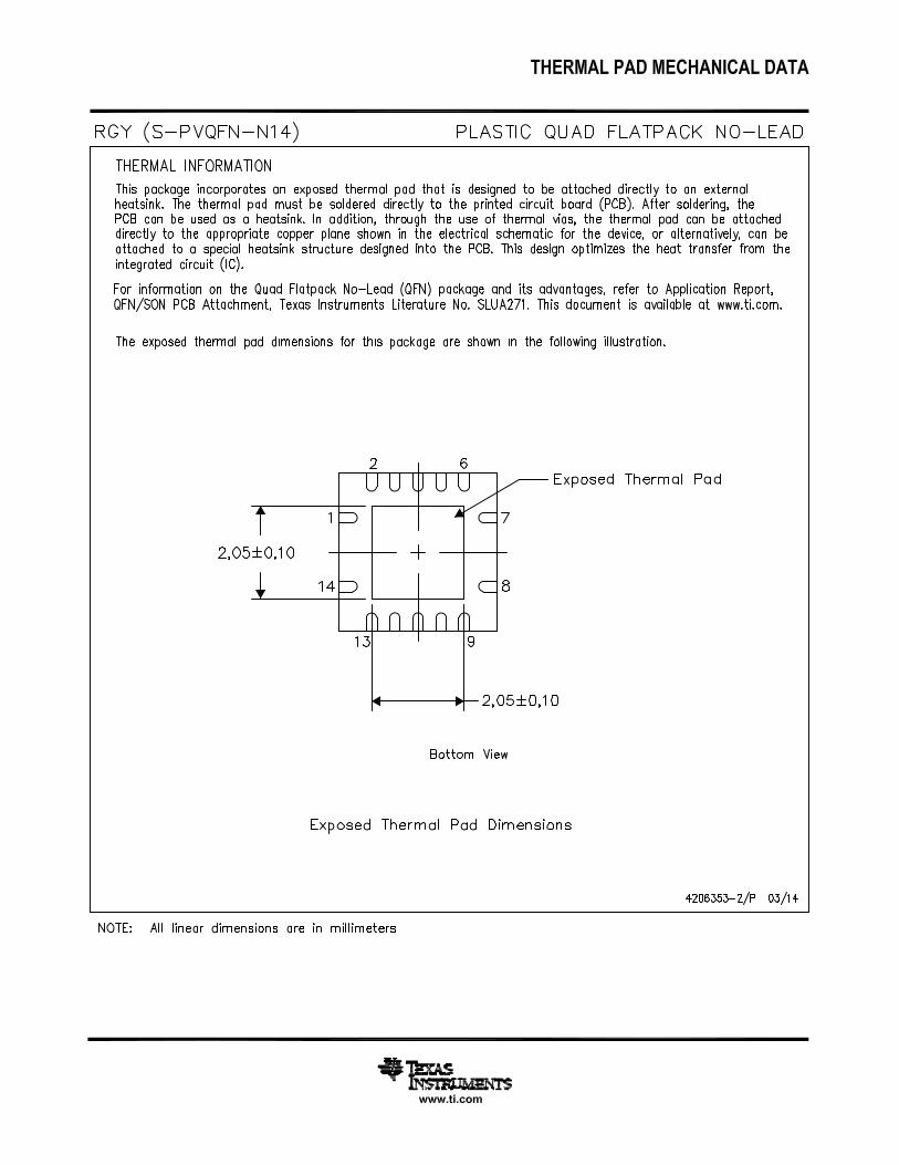
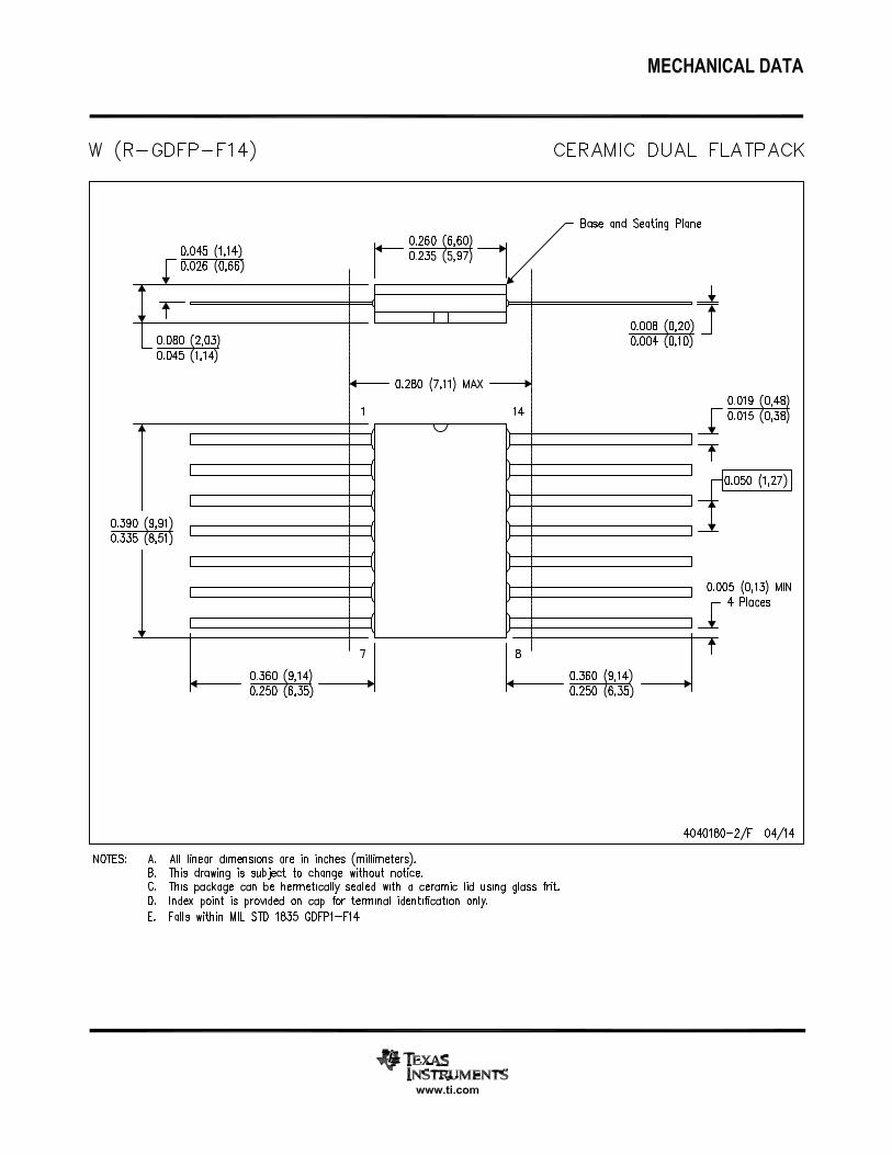
SN54ABT125, SN74ABT125QUADRUPLE BUS BUFFER GATES
WITH 3-STATE OUTPUTSSCBS182I − FEBRUARY 1997 − REVISED NOVEMBER 2002
1POST OFFICE BOX 655303 • DALLAS, TEXAS 75265
� Typical VOLP (Output Ground Bounce)<1 V at VCC = 5 V, TA = 25°C
� High-Drive Outputs (−32-mA IOH, 64-mA IOL)
� Ioff and Power-Up 3-State Support HotInsertion
� Latch-Up Performance Exceeds 500 mA PerJEDEC Standard JESD-17
� ESD Protection Exceeds JESD 22− 2000-V Human-Body Model (A114-A)− 200-V Machine Model (A115-A)
SN54ABT125 . . . J OR W PACKAGESN74ABT125 . . . D, DB, N, NS,
OR PW PACKAGE(TOP VIEW)
1
2
3
4
5
6
7
14
13
12
11
10
9
8
1OE1A1Y
2OE2A2Y
GND
VCC
4OE4A4Y3OE3A3Y
3 2 1 20 19
9 10 11 12 13
4
5
6
7
8
18
17
16
15
14
4ANC4YNC3OE
1YNC
2OENC2A
1A 1OE
NC
3Y 3AV 4O
E
2YG
ND
NC
SN54ABT125 . . . FK PACKAGE(TOP VIEW)
CC
NC − No internal connection
SN74ABT125 . . . RGY PACKAGE(TOP VIEW)
1 14
7 8
2
3
4
5
6
13
12
11
10
9
4OE4A4Y3OE3A
1A1Y
2OE2A2Y
1OE
3YV
GN
D
CC
description/ordering information
The ’ABT125 quadruple bus buffer gates feature independent line drivers with 3-state outputs. Each output isdisabled when the associated output-enable (OE) input is high.
These devices are fully specified for hot-insertion applications using Ioff and power-up 3-state. The Ioff circuitrydisables the outputs, preventing damaging current backflow through the devices when they are powered down.The power-up 3-state circuitry places the outputs in the high-impedance state during power up and power down,which prevents driver conflict.
To ensure the high-impedance state during power up or power down, OE should be tied to VCC through a pullupresistor; the minimum value of the resistor is determined by the current-sinking capability of the driver.
ORDERING INFORMATION
TA PACKAGE† ORDERABLEPART NUMBER
TOP-SIDEMARKING
PDIP − N Tube SN74ABT125N SN74ABT125N
QFN − RGY Tape and reel SN74ABT125RGYR AB125
SOIC DTube SN74ABT125D
ABT125−40°C to 85°C
SOIC − DTape and reel SN74ABT125DR
ABT12540 C to 85 C
SOP − NS Tape and reel SN74ABT125NSR ABT125
SSOP − DB Tape and reel SN74ABT125DBR AB125
TSSOP − PW Tape and reel SN74ABT125PWR AB125
CDIP − J Tube SNJ54ABT125J SNJ54ABT125J
−55°C to 125°C CFP − W Tube SNJ54ABT125W SNJ54ABT125W
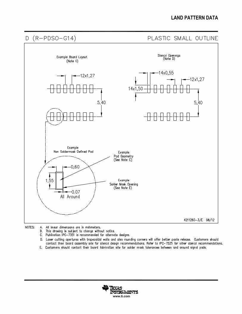
LCCC − FK Tube SNJ54ABT125FK SNJ54ABT125FK† Package drawings, standard packing quantities, thermal data, symbolization, and PCB design
guidelines are available at www.ti.com/sc/package.
Copyright © 2002, Texas Instruments IncorporatedPRODUCTION DATA information is current as of publication date.Products conform to specifications per the terms of Texas Instrumentsstandard warranty. Production processing does not necessarily includetesting of all parameters.
Please be aware that an important notice concerning availability, standard warranty, and use in critical applications ofTexas Instruments semiconductor products and disclaimers thereto appears at the end of this data sheet.
On products compliant to MIL-PRF-38535, all parameters are testedunless otherwise noted. On all other products, productionprocessing does not necessarily include testing of all parameters.

SN54ABT125, SN74ABT125QUADRUPLE BUS BUFFER GATESWITH 3-STATE OUTPUTSSCBS182I − FEBRUARY 1997 − REVISED NOVEMBER 2002
2 POST OFFICE BOX 655303 • DALLAS, TEXAS 75265
FUNCTION TABLE(each buffer)
INPUTS OUTPUTOE A
OUTPUTY
L H H
L L L
H X Z
logic diagram (positive logic)
11OE
21A 1Y
3
42OE
52A 2Y
6
103OE
93A 3Y
8
134OE
124A 4Y
11
Pin numbers shown are for the D, DB, J, N, NS, PW, RGY, and W packages.
absolute maximum ratings over operating free-air temperature range (unless otherwise noted)†
Supply voltage range, VCC −0.5 V to 7 V. . . . . . . . . . . . . . . . . . . . . . . . . . . . . . . . . . . . . . . . . . . . . . . . . . . . . . . . . . Input voltage range, VI (see Note 1) −0.5 V to 7 V. . . . . . . . . . . . . . . . . . . . . . . . . . . . . . . . . . . . . . . . . . . . . . . . . . Voltage range applied to any output in the high or power-off state, VO −0.5 V to 5.5 V. . . . . . . . . . . . . . . . . . . . Current into any output in the low state, IO: SN54ABT125 96 mA. . . . . . . . . . . . . . . . . . . . . . . . . . . . . . . . . . . .
SN74ABT125 128 mA. . . . . . . . . . . . . . . . . . . . . . . . . . . . . . . . . . . Input clamp current, IIK (VI < 0) −18 mA. . . . . . . . . . . . . . . . . . . . . . . . . . . . . . . . . . . . . . . . . . . . . . . . . . . . . . . . . . . Output clamp current, IOK (VO < 0) −50 mA. . . . . . . . . . . . . . . . . . . . . . . . . . . . . . . . . . . . . . . . . . . . . . . . . . . . . . . . Package thermal impedance, θJA (see Note 2): D package 86°C/W. . . . . . . . . . . . . . . . . . . . . . . . . . . . . . . . . . .
(see Note 2): DB package 96°C/W. . . . . . . . . . . . . . . . . . . . . . . . . . . . . . . . . (see Note 2): N package 80°C/W. . . . . . . . . . . . . . . . . . . . . . . . . . . . . . . . . . . (see Note 2): NS package 76°C/W. . . . . . . . . . . . . . . . . . . . . . . . . . . . . . . . . (see Note 2): PW package 113°C/W. . . . . . . . . . . . . . . . . . . . . . . . . . . . . . . . (see Note 3): RGY package 47°C/W. . . . . . . . . . . . . . . . . . . . . . . . . . . . . . . .
Storage temperature range, Tstg −65°C to 150°C. . . . . . . . . . . . . . . . . . . . . . . . . . . . . . . . . . . . . . . . . . . . . . . . . . . † Stresses beyond those listed under “absolute maximum ratings” may cause permanent damage to the device. These are stress ratings only, and
functional operation of the device at these or any other conditions beyond those indicated under “recommended operating conditions” is notimplied. Exposure to absolute-maximum-rated conditions for extended periods may affect device reliability.
NOTES: 1. The input and output negative-voltage ratings may be exceeded if the input and output clamp-current ratings are observed.2. The package thermal impedance is calculated in accordance with JESD 51-7.3. The package thermal impedance is calculated in accordance with JESD 51-5.

SN54ABT125, SN74ABT125QUADRUPLE BUS BUFFER GATES
WITH 3-STATE OUTPUTSSCBS182I − FEBRUARY 1997 − REVISED NOVEMBER 2002
3POST OFFICE BOX 655303 • DALLAS, TEXAS 75265
recommended operating conditions (see Note 4)
SN54ABT125 SN74ABT125UNIT
MIN MAX MIN MAXUNIT
VCC Supply voltage 4.5 5.5 4.5 5.5 V
VIH High-level input voltage 2 2 V
VIL Low-level input voltage 0.8 0.8 V
VI Input voltage 0 VCC 0 VCC V
IOH High-level output current −24 −32 mA
IOL Low-level output current 48 64 mA
Δt/Δv Input transition rise or fall rate 10 10 ns/V
Δt/ΔVCC Power-up ramp rate 200 200 μs/V
TA Operating free-air temperature −55 125 −40 85 °C
NOTE 4: All unused inputs of the device must be held at VCC or GND to ensure proper device operation. Refer to the TI application report,Implications of Slow or Floating CMOS Inputs, literature number SCBA004.

SN54ABT125, SN74ABT125QUADRUPLE BUS BUFFER GATESWITH 3-STATE OUTPUTSSCBS182I − FEBRUARY 1997 − REVISED NOVEMBER 2002
4 POST OFFICE BOX 655303 • DALLAS, TEXAS 75265
electrical characteristics over recommended operating free-air temperature range (unlessotherwise noted)
PARAMETER TEST CONDITIONSTA = 25°C SN54ABT125 SN74ABT125
UNITPARAMETER TEST CONDITIONSMIN TYP† MAX MIN MAX MIN MAX
UNIT
VIK VCC = 4.5 V, II = −18 mA −1.2 −1.2 −1.2 V
VCC = 4.5 V, IOH = −3 mA 2.5 2.5 2.5
VVCC = 5 V, IOH = −3 mA 3 3 3
VVOH
V 4 5 VIOH = −24 mA 2 2
V
VCC = 4.5 VIOH = −32 mA 2* 2
V V 4 5 VIOL = 48 mA 0.55 0.55
VVOL VCC = 4.5 VIOL = 64 mA 0.55* 0.55
V
Vhys 100 mV
II VCC = 0 to 5.5 V, VI = VCC or GND ±1 ±1 ±1 μA
IOZPU VCC = 0 to 2.1 V, VO = 0.5 V to 2.7 V, OE = X ±50 ±50 ±50 μA
IOZPD VCC = 2.1 V to 0, VO = 0.5 V to 2.7 V, OE = X ±50 ±50 ±50 μA
IOZH VCC = 2.1 V to 5.5 V, VO = 2.7 V, OE ≥ 2 V 10 10 10 μA
IOZL VCC = 2.1 V to 5.5 V, VO = 0.5 V, OE ≥ 2 V −10 −10 −10 μA
Ioff VCC = 0, VI or VO ≤ 4.5 V ±100 ±100 μA
ICEXVCC = 5.5 V,VO = 5.5 V
Outputs high 50 50 50 μA
IO‡ VCC = 5.5 V, VO = 2.5 V −50 −100 −200§ −50 −200§ −50 −200§ mA
VCC = 5.5 V, Outputs high 1 250 250 250 μA
ICC
VCC = 5.5 V,IO = 0, Outputs low 24 30 30 30 mAICC IO 0,VI = VCC or GND Outputs disabled 0.5 250 250 250 μA
DataVCC = 5.5 V,One input at 3.4 V,
Outputs enabled 1.5 1.5 1.5
ΔICC¶
Datainputs
One input at 3.4 V,Other inputs atVCC or GND Outputs disabled 0.05 0.05 0.05 mA
Controlinputs
VCC = 5.5 V, One input at 3.4 V,Other inputs at VCC or GND
1.5 1.5 1.5
Ci VI = 2.5 V or 0.5 V 3 pF
Co VO = 2.5 V or 0.5 V 7 pF
* On products compliant to MIL-PRF-38535, this parameter does not apply.† All typical values are at VCC = 5 V.‡ Not more than one output should be tested at a time, and the duration of the test should not exceed one second.§ This limit may vary among suppliers.¶ This is the increase in supply current for each input that is at the specified TTL voltage level, rather than VCC or GND.

SN54ABT125, SN74ABT125QUADRUPLE BUS BUFFER GATES
WITH 3-STATE OUTPUTSSCBS182I − FEBRUARY 1997 − REVISED NOVEMBER 2002
5POST OFFICE BOX 655303 • DALLAS, TEXAS 75265
switching characteristics over recommended ranges of supply voltage and operating free-airtemperature (unless otherwise noted) (see Figure 1)
PARAMETERFROM
(INPUT)TO
(OUTPUT)
VCC = 5 V,TA = 25°C SN54ABT125 SN74ABT125
UNITPARAMETER(INPUT) (OUTPUT)
MIN TYP MAX MIN MAX MIN MAXUNIT
tPLH†
A Y1 3.2 4.6 1 6 1 4.9
nstPHL
† A Y1 2.5 4.6 1 6.2 1 4.9
ns
tPZH†
OE Y1 3.6 5 1 6 1 5.9
nstPZL
† OE Y1 2.5 6.2 1 7.5 1 6.8
ns
tPHZOE Y
1 3.8 5.4 1 6.3 1 6.2ns
tPLZ† OE Y
1 3.3 5.3 1 6.5 1 6.2ns
† This limit may vary among suppliers.

SN54ABT125, SN74ABT125QUADRUPLE BUS BUFFER GATESWITH 3-STATE OUTPUTSSCBS182I − FEBRUARY 1997 − REVISED NOVEMBER 2002
6 POST OFFICE BOX 655303 • DALLAS, TEXAS 75265
PARAMETER MEASUREMENT INFORMATION
1.5 V
thtsu
From Output Under Test
CL = 50 pF(see Note A)
LOAD CIRCUIT
S1
7 V
Open
GND
500 Ω
500 Ω
Data Input
Timing Input 1.5 V3 V
0 V
1.5 V 1.5 V
3 V
0 V
3 V
0 V
1.5 V
tw
Input
VOLTAGE WAVEFORMSSETUP AND HOLD TIMES
VOLTAGE WAVEFORMSPROPAGATION DELAY TIMES
INVERTING AND NONINVERTING OUTPUTS
VOLTAGE WAVEFORMSPULSE DURATION
tPLH
tPHL
tPHL
tPLH
VOH
VOH
VOL
VOL
1.5 V 1.5 V
3 V
0 V
1.5 V1.5 V
Input
1.5 V
OutputControl
OutputWaveform 1
S1 at 7 V(see Note B)
OutputWaveform 2S1 at Open
(see Note B)
VOL
VOH
tPZL
tPZH
tPLZ
tPHZ
1.5 V1.5 V
3.5 V
0 V
1.5 V VOL + 0.3 V
1.5 V VOH − 0.3 V
≈0 V
3 V
VOLTAGE WAVEFORMSENABLE AND DISABLE TIMES
LOW- AND HIGH-LEVEL ENABLING
Output
Output
tPLH/tPHLtPLZ/tPZLtPHZ/tPZH
Open7 V
Open
TEST S1
NOTES: A. CL includes probe and jig capacitance.B. Waveform 1 is for an output with internal conditions such that the output is low except when disabled by the output control.
Waveform 2 is for an output with internal conditions such that the output is high except when disabled by the output control.C. All input pulses are supplied by generators having the following characteristics: PRR ≤ 10 MHz, ZO = 50 Ω, tr ≤ 2.5 ns, tf ≤ 2.5 ns.D. The outputs are measured one at a time with one transition per measurement.E. All parameters and waveforms are not applicable to all devices.
1.5 V
Figure 1. Load Circuit and Voltage Waveforms

PACKAGE OPTION ADDENDUM
www.ti.com 24-Aug-2018
Addendum-Page 1
PACKAGING INFORMATION
Orderable Device Status(1)
Package Type PackageDrawing
Pins PackageQty
Eco Plan(2)
Lead/Ball Finish(6)
MSL Peak Temp(3)
Op Temp (°C) Device Marking(4/5)
Samples
5962-9676801Q2A ACTIVE LCCC FK 20 1 TBD POST-PLATE N / A for Pkg Type -55 to 125 5962-9676801Q2ASNJ54ABT125FK
5962-9676801QCA ACTIVE CDIP J 14 1 TBD A42 N / A for Pkg Type -55 to 125 5962-9676801QCASNJ54ABT125J
5962-9676801QDA ACTIVE CFP W 14 1 TBD A42 N / A for Pkg Type -55 to 125 5962-9676801QDASNJ54ABT125W
SN74ABT125D ACTIVE SOIC D 14 50 Green (RoHS& no Sb/Br)
CU NIPDAU Level-1-260C-UNLIM -40 to 85 ABT125
SN74ABT125DBR ACTIVE SSOP DB 14 2000 Green (RoHS& no Sb/Br)
CU NIPDAU Level-1-260C-UNLIM -40 to 85 AB125
SN74ABT125DE4 ACTIVE SOIC D 14 50 Green (RoHS& no Sb/Br)
CU NIPDAU Level-1-260C-UNLIM -40 to 85 ABT125
SN74ABT125DG4 ACTIVE SOIC D 14 50 Green (RoHS& no Sb/Br)
CU NIPDAU Level-1-260C-UNLIM -40 to 85 ABT125
SN74ABT125DR ACTIVE SOIC D 14 2500 Green (RoHS& no Sb/Br)
CU NIPDAU Level-1-260C-UNLIM -40 to 85 ABT125
SN74ABT125DRE4 ACTIVE SOIC D 14 2500 Green (RoHS& no Sb/Br)
CU NIPDAU Level-1-260C-UNLIM -40 to 85 ABT125
SN74ABT125DRG4 ACTIVE SOIC D 14 2500 Green (RoHS& no Sb/Br)
CU NIPDAU Level-1-260C-UNLIM -40 to 85 ABT125
SN74ABT125N ACTIVE PDIP N 14 25 Green (RoHS& no Sb/Br)
CU NIPDAU N / A for Pkg Type -40 to 85 SN74ABT125N
SN74ABT125NSR ACTIVE SO NS 14 2000 Green (RoHS& no Sb/Br)
CU NIPDAU Level-1-260C-UNLIM -40 to 85 ABT125
SN74ABT125PW ACTIVE TSSOP PW 14 90 Green (RoHS& no Sb/Br)
CU NIPDAU Level-1-260C-UNLIM -40 to 85 AB125
SN74ABT125PWG4 ACTIVE TSSOP PW 14 90 Green (RoHS& no Sb/Br)
CU NIPDAU Level-1-260C-UNLIM -40 to 85 AB125
SN74ABT125PWR ACTIVE TSSOP PW 14 2000 Green (RoHS& no Sb/Br)
CU NIPDAU Level-1-260C-UNLIM -40 to 85 AB125

PACKAGE OPTION ADDENDUM
www.ti.com 24-Aug-2018
Addendum-Page 2
Orderable Device Status(1)
Package Type PackageDrawing
Pins PackageQty
Eco Plan(2)
Lead/Ball Finish(6)
MSL Peak Temp(3)
Op Temp (°C) Device Marking(4/5)
Samples
SN74ABT125PWRE4 ACTIVE TSSOP PW 14 2000 Green (RoHS& no Sb/Br)
CU NIPDAU Level-1-260C-UNLIM -40 to 85 AB125
SN74ABT125PWRG4 ACTIVE TSSOP PW 14 2000 Green (RoHS& no Sb/Br)
CU NIPDAU Level-1-260C-UNLIM -40 to 85 AB125
SN74ABT125RGYR ACTIVE VQFN RGY 14 3000 Green (RoHS& no Sb/Br)
CU NIPDAU Level-2-260C-1 YEAR -40 to 85 AB125
SNJ54ABT125FK ACTIVE LCCC FK 20 1 TBD POST-PLATE N / A for Pkg Type -55 to 125 5962-9676801Q2ASNJ54ABT125FK
SNJ54ABT125J ACTIVE CDIP J 14 1 TBD A42 N / A for Pkg Type -55 to 125 5962-9676801QCASNJ54ABT125J
SNJ54ABT125W ACTIVE CFP W 14 1 TBD A42 N / A for Pkg Type -55 to 125 5962-9676801QDASNJ54ABT125W
(1) The marketing status values are defined as follows:ACTIVE: Product device recommended for new designs.LIFEBUY: TI has announced that the device will be discontinued, and a lifetime-buy period is in effect.NRND: Not recommended for new designs. Device is in production to support existing customers, but TI does not recommend using this part in a new design.PREVIEW: Device has been announced but is not in production. Samples may or may not be available.OBSOLETE: TI has discontinued the production of the device.
(2) RoHS: TI defines "RoHS" to mean semiconductor products that are compliant with the current EU RoHS requirements for all 10 RoHS substances, including the requirement that RoHS substancedo not exceed 0.1% by weight in homogeneous materials. Where designed to be soldered at high temperatures, "RoHS" products are suitable for use in specified lead-free processes. TI mayreference these types of products as "Pb-Free".RoHS Exempt: TI defines "RoHS Exempt" to mean products that contain lead but are compliant with EU RoHS pursuant to a specific EU RoHS exemption.Green: TI defines "Green" to mean the content of Chlorine (Cl) and Bromine (Br) based flame retardants meet JS709B low halogen requirements of <=1000ppm threshold. Antimony trioxide basedflame retardants must also meet the <=1000ppm threshold requirement.
(3) MSL, Peak Temp. - The Moisture Sensitivity Level rating according to the JEDEC industry standard classifications, and peak solder temperature.
(4) There may be additional marking, which relates to the logo, the lot trace code information, or the environmental category on the device.
(5) Multiple Device Markings will be inside parentheses. Only one Device Marking contained in parentheses and separated by a "~" will appear on a device. If a line is indented then it is a continuationof the previous line and the two combined represent the entire Device Marking for that device.

PACKAGE OPTION ADDENDUM
www.ti.com 24-Aug-2018
Addendum-Page 3
(6) Lead/Ball Finish - Orderable Devices may have multiple material finish options. Finish options are separated by a vertical ruled line. Lead/Ball Finish values may wrap to two lines if the finishvalue exceeds the maximum column width.
Important Information and Disclaimer:The information provided on this page represents TI's knowledge and belief as of the date that it is provided. TI bases its knowledge and belief on informationprovided by third parties, and makes no representation or warranty as to the accuracy of such information. Efforts are underway to better integrate information from third parties. TI has taken andcontinues to take reasonable steps to provide representative and accurate information but may not have conducted destructive testing or chemical analysis on incoming materials and chemicals.TI and TI suppliers consider certain information to be proprietary, and thus CAS numbers and other limited information may not be available for release.
In no event shall TI's liability arising out of such information exceed the total purchase price of the TI part(s) at issue in this document sold by TI to Customer on an annual basis.
OTHER QUALIFIED VERSIONS OF SN54ABT125, SN74ABT125 :
• Catalog: SN74ABT125
• Military: SN54ABT125
NOTE: Qualified Version Definitions:
• Catalog - TI's standard catalog product
• Military - QML certified for Military and Defense Applications

TAPE AND REEL INFORMATION
*All dimensions are nominal
Device PackageType
PackageDrawing
Pins SPQ ReelDiameter
(mm)
ReelWidth
W1 (mm)
A0(mm)
B0(mm)
K0(mm)
P1(mm)
W(mm)
Pin1Quadrant
SN74ABT125DBR SSOP DB 14 2000 330.0 16.4 8.2 6.6 2.5 12.0 16.0 Q1
SN74ABT125DR SOIC D 14 2500 330.0 16.4 6.5 9.0 2.1 8.0 16.0 Q1
SN74ABT125DR SOIC D 14 2500 330.0 16.4 6.5 9.0 2.1 8.0 16.0 Q1
SN74ABT125NSR SO NS 14 2000 330.0 16.4 8.2 10.5 2.5 12.0 16.0 Q1
SN74ABT125PWR TSSOP PW 14 2000 330.0 12.4 6.9 5.6 1.6 8.0 12.0 Q1
SN74ABT125RGYR VQFN RGY 14 3000 330.0 12.4 3.75 3.75 1.15 8.0 12.0 Q1
PACKAGE MATERIALS INFORMATION
www.ti.com 14-Jul-2012
Pack Materials-Page 1

*All dimensions are nominal
Device Package Type Package Drawing Pins SPQ Length (mm) Width (mm) Height (mm)
SN74ABT125DBR SSOP DB 14 2000 367.0 367.0 38.0
SN74ABT125DR SOIC D 14 2500 367.0 367.0 38.0
SN74ABT125DR SOIC D 14 2500 333.2 345.9 28.6
SN74ABT125NSR SO NS 14 2000 367.0 367.0 38.0
SN74ABT125PWR TSSOP PW 14 2000 367.0 367.0 35.0
SN74ABT125RGYR VQFN RGY 14 3000 367.0 367.0 35.0
PACKAGE MATERIALS INFORMATION
www.ti.com 14-Jul-2012
Pack Materials-Page 2


www.ti.com
PACKAGE OUTLINE
C
14X .008-.014 [0.2-0.36]TYP
-150
AT GAGE PLANE
-.314.308-7.977.83[ ]
14X -.026.014-0.660.36[ ]14X -.065.045
-1.651.15[ ]
.2 MAX TYP[5.08]
.13 MIN TYP[3.3]
TYP-.060.015-1.520.38[ ]
4X .005 MIN[0.13]
12X .100[2.54]
.015 GAGE PLANE[0.38]
A
-.785.754-19.9419.15[ ]
B -.283.245-7.196.22[ ]
CDIP - 5.08 mm max heightJ0014ACERAMIC DUAL IN LINE PACKAGE
4214771/A 05/2017
NOTES: 1. All controlling linear dimensions are in inches. Dimensions in brackets are in millimeters. Any dimension in brackets or parenthesis are for reference only. Dimensioning and tolerancing per ASME Y14.5M.2. This drawing is subject to change without notice. 3. This package is hermitically sealed with a ceramic lid using glass frit.4. Index point is provided on cap for terminal identification only and on press ceramic glass frit seal only.5. Falls within MIL-STD-1835 and GDIP1-T14.
7 8
141
PIN 1 ID(OPTIONAL)
SCALE 0.900
SEATING PLANE
.010 [0.25] C A B

www.ti.com
EXAMPLE BOARD LAYOUT
ALL AROUND[0.05]
MAX.002
.002 MAX[0.05]ALL AROUND
SOLDER MASKOPENING
METAL
(.063)[1.6]
(R.002 ) TYP[0.05]
14X ( .039)[1]
( .063)[1.6]
12X (.100 )[2.54]
(.300 ) TYP[7.62]
CDIP - 5.08 mm max heightJ0014ACERAMIC DUAL IN LINE PACKAGE
4214771/A 05/2017
LAND PATTERN EXAMPLENON-SOLDER MASK DEFINED
SCALE: 5X
SEE DETAIL A SEE DETAIL B
SYMM
SYMM
1
7 8
14
DETAIL ASCALE: 15X
SOLDER MASKOPENING
METAL
DETAIL B13X, SCALE: 15X


MECHANICAL DATA
MSSO002E – JANUARY 1995 – REVISED DECEMBER 2001
POST OFFICE BOX 655303 • DALLAS, TEXAS 75265
DB (R-PDSO-G**) PLASTIC SMALL-OUTLINE
4040065 /E 12/01
28 PINS SHOWN
Gage Plane
8,207,40
0,550,95
0,25
38
12,90
12,30
28
10,50
24
8,50
Seating Plane
9,907,90
30
10,50
9,90
0,38
5,605,00
15
0,22
14
A
28
1
2016
6,506,50
14
0,05 MIN
5,905,90
DIM
A MAX
A MIN
PINS **
2,00 MAX
6,90
7,50
0,65 M0,15
0°–�8°
0,10
0,090,25
NOTES: A. All linear dimensions are in millimeters.B. This drawing is subject to change without notice.C. Body dimensions do not include mold flash or protrusion not to exceed 0,15.D. Falls within JEDEC MO-150

IMPORTANT NOTICE
Texas Instruments Incorporated (TI) reserves the right to make corrections, enhancements, improvements and other changes to itssemiconductor products and services per JESD46, latest issue, and to discontinue any product or service per JESD48, latest issue. Buyersshould obtain the latest relevant information before placing orders and should verify that such information is current and complete.TI’s published terms of sale for semiconductor products (http://www.ti.com/sc/docs/stdterms.htm) apply to the sale of packaged integratedcircuit products that TI has qualified and released to market. Additional terms may apply to the use or sale of other types of TI products andservices.Reproduction of significant portions of TI information in TI data sheets is permissible only if reproduction is without alteration and isaccompanied by all associated warranties, conditions, limitations, and notices. TI is not responsible or liable for such reproduceddocumentation. Information of third parties may be subject to additional restrictions. Resale of TI products or services with statementsdifferent from or beyond the parameters stated by TI for that product or service voids all express and any implied warranties for theassociated TI product or service and is an unfair and deceptive business practice. TI is not responsible or liable for any such statements.Buyers and others who are developing systems that incorporate TI products (collectively, “Designers”) understand and agree that Designersremain responsible for using their independent analysis, evaluation and judgment in designing their applications and that Designers havefull and exclusive responsibility to assure the safety of Designers' applications and compliance of their applications (and of all TI productsused in or for Designers’ applications) with all applicable regulations, laws and other applicable requirements. Designer represents that, withrespect to their applications, Designer has all the necessary expertise to create and implement safeguards that (1) anticipate dangerousconsequences of failures, (2) monitor failures and their consequences, and (3) lessen the likelihood of failures that might cause harm andtake appropriate actions. Designer agrees that prior to using or distributing any applications that include TI products, Designer willthoroughly test such applications and the functionality of such TI products as used in such applications.TI’s provision of technical, application or other design advice, quality characterization, reliability data or other services or information,including, but not limited to, reference designs and materials relating to evaluation modules, (collectively, “TI Resources”) are intended toassist designers who are developing applications that incorporate TI products; by downloading, accessing or using TI Resources in anyway, Designer (individually or, if Designer is acting on behalf of a company, Designer’s company) agrees to use any particular TI Resourcesolely for this purpose and subject to the terms of this Notice.TI’s provision of TI Resources does not expand or otherwise alter TI’s applicable published warranties or warranty disclaimers for TIproducts, and no additional obligations or liabilities arise from TI providing such TI Resources. TI reserves the right to make corrections,enhancements, improvements and other changes to its TI Resources. TI has not conducted any testing other than that specificallydescribed in the published documentation for a particular TI Resource.Designer is authorized to use, copy and modify any individual TI Resource only in connection with the development of applications thatinclude the TI product(s) identified in such TI Resource. NO OTHER LICENSE, EXPRESS OR IMPLIED, BY ESTOPPEL OR OTHERWISETO ANY OTHER TI INTELLECTUAL PROPERTY RIGHT, AND NO LICENSE TO ANY TECHNOLOGY OR INTELLECTUAL PROPERTYRIGHT OF TI OR ANY THIRD PARTY IS GRANTED HEREIN, including but not limited to any patent right, copyright, mask work right, orother intellectual property right relating to any combination, machine, or process in which TI products or services are used. Informationregarding or referencing third-party products or services does not constitute a license to use such products or services, or a warranty orendorsement thereof. Use of TI Resources may require a license from a third party under the patents or other intellectual property of thethird party, or a license from TI under the patents or other intellectual property of TI.TI RESOURCES ARE PROVIDED “AS IS” AND WITH ALL FAULTS. TI DISCLAIMS ALL OTHER WARRANTIES ORREPRESENTATIONS, EXPRESS OR IMPLIED, REGARDING RESOURCES OR USE THEREOF, INCLUDING BUT NOT LIMITED TOACCURACY OR COMPLETENESS, TITLE, ANY EPIDEMIC FAILURE WARRANTY AND ANY IMPLIED WARRANTIES OFMERCHANTABILITY, FITNESS FOR A PARTICULAR PURPOSE, AND NON-INFRINGEMENT OF ANY THIRD PARTY INTELLECTUALPROPERTY RIGHTS. TI SHALL NOT BE LIABLE FOR AND SHALL NOT DEFEND OR INDEMNIFY DESIGNER AGAINST ANY CLAIM,INCLUDING BUT NOT LIMITED TO ANY INFRINGEMENT CLAIM THAT RELATES TO OR IS BASED ON ANY COMBINATION OFPRODUCTS EVEN IF DESCRIBED IN TI RESOURCES OR OTHERWISE. IN NO EVENT SHALL TI BE LIABLE FOR ANY ACTUAL,DIRECT, SPECIAL, COLLATERAL, INDIRECT, PUNITIVE, INCIDENTAL, CONSEQUENTIAL OR EXEMPLARY DAMAGES INCONNECTION WITH OR ARISING OUT OF TI RESOURCES OR USE THEREOF, AND REGARDLESS OF WHETHER TI HAS BEENADVISED OF THE POSSIBILITY OF SUCH DAMAGES.Unless TI has explicitly designated an individual product as meeting the requirements of a particular industry standard (e.g., ISO/TS 16949and ISO 26262), TI is not responsible for any failure to meet such industry standard requirements.Where TI specifically promotes products as facilitating functional safety or as compliant with industry functional safety standards, suchproducts are intended to help enable customers to design and create their own applications that meet applicable functional safety standardsand requirements. Using products in an application does not by itself establish any safety features in the application. Designers mustensure compliance with safety-related requirements and standards applicable to their applications. Designer may not use any TI products inlife-critical medical equipment unless authorized officers of the parties have executed a special contract specifically governing such use.Life-critical medical equipment is medical equipment where failure of such equipment would cause serious bodily injury or death (e.g., lifesupport, pacemakers, defibrillators, heart pumps, neurostimulators, and implantables). Such equipment includes, without limitation, allmedical devices identified by the U.S. Food and Drug Administration as Class III devices and equivalent classifications outside the U.S.TI may expressly designate certain products as completing a particular qualification (e.g., Q100, Military Grade, or Enhanced Product).Designers agree that it has the necessary expertise to select the product with the appropriate qualification designation for their applicationsand that proper product selection is at Designers’ own risk. Designers are solely responsible for compliance with all legal and regulatoryrequirements in connection with such selection.Designer will fully indemnify TI and its representatives against any damages, costs, losses, and/or liabilities arising out of Designer’s non-compliance with the terms and provisions of this Notice.
Mailing Address: Texas Instruments, Post Office Box 655303, Dallas, Texas 75265Copyright © 2018, Texas Instruments Incorporated