oled for lighting - yole développement, mems, · pdf fileoled for lighting technology,...
TRANSCRIPT

From Technologies to Market
OLED for Lighting
Technology, Industry and Market Trends
2016 Report
SAMPLE

2
o Objectives of the report P6
o What’s new compared to “OLED for Lighting” 2012 report? P7
o Authors of the report P8
o Acronym P9
o Executive summary P10
o Introduction to OLED for lighting P36
• Take away
• What is an OLED?
• OLED historical milestones - Focus on OLED lighting
• Applications and market segments of OLEDs
• Why OLED for lighting?
• OLED for lighting challenges
• OLED lighting vs. OLED display - Requirements & Status of technologies
• Key drivers and barriers for OLED lighting
o OLED lighting applications and markets P47
• Introduction
• The Solid State Lighting (SSL) revolution
• Potential for OLEDs
• OLED vs. LED
• Status of LED technology and industry
• Advantages of OLEDs
• Challenges for OLEDs
• Focus on efficacy
• Focus on cost
• General lighting (1/2)
• Take away
• Overview of light source technologies
• Overview of market segments (and associated characteristics)
• General lighting (2/2)
• Market highlights - Current status
• OLED integration
• Market landscape, drivers, customers and applications
• Current main market / product focus
• Analysis of task lamp application (LED vs. OLED)
• Market access roadmap
• Future trends - Flexible OLED lighting panels
• Introduction
• Technology push vs. Market pull
• Flexible system with rigid panels
• Roadmap of applications - Toward flexible and transparent OLEDs
• OLED lighting panel market volume
• OLED lighting panel market size
• Automotive lighting (1/2)
• Take away
• General context
• Drivers & Potential applications
• Challenges for OLED integration (Technology / Market / Industry aspects)
• Recent development
• OLED rear lamp prototypes from HELLA
• OLED rear lamp prototypes from Osram
• OLED rear lamp prototypes from Stanley Electric
• BMW - From prototype to production (M4 GTS)
• Future trends - From 2D OLED to 3D OLED
• OLED lighting panel market volume
• OLED lighting panel market size
• Niche lighting
• Take away
• Analysis
• Total OLED lighting market opportunity
TABLE OF CONTENT OF THE REPORT (1/4)
©2016 | www.yole.fr | OLED for Lighting Report

3
o OLED lighting industry P100
• Take away
• Overview
• OLED equipment developers and suppliers
• OLED material developers and suppliers
• OLED lighting panel developers and suppliers
• OLED lighting module developers and suppliers
• OLED luminaire developers and suppliers
• Partnerships and collaboration
• Advantages
• Status
• South Korea = Centre of gravity for OLED business
• Recent M&A and exits
o OLED structures and materials (1/2) P114
• Take away
• Overview
• Typical structure of an OLED
• OLED working principle
• Bottom-emitting, top-emitting and transparent OLED
• Different approaches to obtain white OLEDs
• Overview of OLED structures and materials
• Organic materials
• Insights on flexible OLEDs
• Why going “flexible”?
• OLED lighting panel from Konica Minolta
• Flexible device vs. Rigid final product
• Which flexible OLED lighting devices do we need?
• Substrate
• Technology push vs. Market pull
• Analysis of potential for flexible OLEDs
• Substrate
• Targeted properties of OLED substrates
• Overview of OLED substrates
• Comparative table
• Flexible OLED substrates challenges
• Overview
• Metal foil
• Rigid glass
• Ultrathin GlassThin
• Integrated OLED substrate
• Anode and cathode
• Material requirements for OLED electrode materials
• Comparison of different materials used for transparent electrodes
• Indium Tin Oxide (ITO) - A standard anode material
• Why ITO alternatives are sought?
• ITO alternatives
• PEDOT:PSS
• Silver nanowires from Cambrios
• Metal grid
• Graphene
• A new candidate for transparent OLED electrode
• Electrode challenge - Complex process integration
• Overview of OLED cathode materials
• Air-stable cathode
• Hole Injection Layer (HIL) and Hole Transport Layer (HTL)
• Hole injection layer
• Material requirements
• PEDOT:PSS as HIL material
• Hole transport layer - Material requirements
TABLE OF CONTENT OF THE REPORT (2/4)
©2016 | www.yole.fr | OLED for Lighting Report
4
o OLED structures and materials (2/2) P114
• Emissive organic materials
• Phosphorescent vs. Fluorescent materials
• Hybrid OLED vs. PHOLED
• Thermally Activated Delayed Fluorescence (TADF)
• White OLED emitter compositions
• Host materials and dopants
• Light-Emitting Polymers (LEPs)
• Insight on the lifetime issues of emitter materials
• Blocking Layer (BL), Electron Transport Layer (ETL) and Electron Injection Layer (EIL)
• Blocking layer
• Electron transport layer
• Electron injection layer
• Encapsulation
• Overview
• Barrier material requirements
• Encapsulation structures and materials
• Alternatives to a glass barrier
• Multilayer barrier solution
• Barrier technology solutions and associated companies
• Why so many companies focus on barrier development?
• Challenges associated with barrier quality measurements
• Light extraction
• Light extraction structures
• Types of light out-coupling structures
o OLED manufacturing techniques and equipment (1/2) P185
• Overview of techniques and equipment
• Take away
• Importance of the matching of the materials and equipment
• Manufacturing process flow for OLED lighting panel
• OLED lighting panel production
• Manufacturing process line for the OLED display
• Patterning
• OLED panel size scaling
• The largest rigid and flexible OLED panels in 2016
• Technology challenges in OLED panel size scaling
• Market challenges in OLED panel size scaling
• OLED electronic drivers
• Sheet-to-sheet vs. Roll-to-roll techniques
• Sheet-to-sheet process for OLED on flexible substrates
• Thin film deposition - Digital growth vs. Photolithography approach
• OLED testing and sorting
• Overview of deposition techniques used for OLEDs
• Dry deposition vs. Solution deposition
• Vapor deposition of organic layers
• Overview
• Characteristics
• Vapor Thermal Evaporation (VTE)
• Linear evaporation sources to achieve higher throughput
• Organic Vapor Phase Deposition (OVPD®)
• Overview
• Focus on Aixtron OVPD® equipment
• Polymer Vapor Phase Deposition (PVPD™)
TABLE OF CONTENT OF THE REPORT (3/4)
©2016 | www.yole.fr | OLED for Lighting Report
5
o OLED manufacturing techniques and equipment (2/2) P185
• Solution-based deposition techniques
• Take away
• Requirements for film formation
• Challenges of multilayer deposition
• Approaches for multilayer deposition
• Orthogonal solvents approach
• Crosslinking approach
• Spin-coating
• Inkjet printing
• Overview
• Focus on Kateeva
• Focus on Sumitomo Chemical
• Slot die coating
• Other techniques
o OLED manufacturing cost P223
• Take away
• Introduction
• 2013 - 2021 OLED lighting panel manufacturing cost ($/m²)
• Overview
• Process cost
• Material cost
• Industrial roadmaps
• Analysis
• How to decrease OLED lighting panel manufacturing cost?
• Key milestones
o OLED roadmap and R&D activities P236
• Take away
• State-of-the-art of OLED lighting
• Challenges associated to OLED lighting
• Roadmap
• Introduction
• Key milestones achieved & Next steps
• Focus on efficacy
• Analysis
• The different approaches to achieve low OLED cost
• The different ways to improved OLED efficacy
• Main financing institutions / organizations for OLED lighting R&D Activities
o General conclusion P247
TABLE OF CONTENT OF THE REPORT (4/4)
©2016 | www.yole.fr | OLED for Lighting Report

6
This objective of this report is to provide a comprehensive overview of all aspects of OLED lighting!
Deep insight into various OLED technology approaches (materials, structures, equipment, manufacturing techniques) and their comparison + Analysis of industry, technology roadmaps and market metrics.
• Organic Light Emitting Diode (OLED) technology has a potential for innovative lightweight, very thin, and even flexible and transparent lighting sources.However, many challenges must be overcome to bring this technology to the lighting market (e.g..: general lighting, automotive lighting…).
• Currently the huge number of technology choices for OLED make technology selection difficult. Possible technology selections include: OLED based on varioussubstrates, electrode materials, organic emissive materials, encapsulation solutions, OLED structures and manufacturing processes and techniques used.Moreover, the industrial supply chain is still very dispersed with many players only specialized in a part of the supply chain.
• Continuously improving other lighting technologies, such as inorganic LEDs, make the penetration of OLEDs difficult and market estimations for OLEDs evenmore difficult.
The objectives of this report are:
• To analyze current status of OLEDs for lighting applications, and future trends!
• To analyze OLED lighting industry structure and future trends!
• To analyze main materials and structures used for OLED lighting panels development / manufacturing!
• To analyze main manufacturing techniques and equipment used for OLED lighting panels development!
• To analyze manufacturing costs related to OLED lighting panels.
• To analyze OLED lighting roadmaps and R&D activities.
• To provide volume / size for OLED lighting panels!
OBJECTIVES OF THE REPORT
©2016 | www.yole.fr | OLED for Lighting Report

7
• Updated analysis of OLED lighting applications and market
+ Strong focus on automotive lighting
+ New analysis on potential of flexible OLEDs in lighting applications
+ New analysis on niche lighting applications
• Updated analysis of OLED lighting industry
+ New analysis on recent M&A and exits
• Updated analysis of OLED materials and structures
+ New analysis on flexible OLED, encapsulation,TADF material, graphene material (…)
• Updated analysis of OLED manufacturing techniques
+ New analysis on solution-based process / techniques
• Updated analysis of OLED manufacturing cost
• Updated analysis of OLED roadmaps and R&D activities
WHAT’S NEW COMPARED TO “OLED FOR LIGHTING” 2012 REPORT?
©2016 | www.yole.fr | OLED for Lighting Report

8
Pars MUKISH (Business Unit Manager - Sapphire, LED / OLED, Display and Lighting Systems -Yole Développement)
• Pars MUKISH holds a master’s degree in Materials Science & Polymers from ITECH in France and a master’s degree in Innovation &Technology Management from EM Lyon, also in France. He works at Yole Développement, the "More than Moore" market researchand strategy consulting company, as Senior Market and Technology Analyst in the fields of LED, OLED, Lighting Technologies andCompound Semiconductors, carrying out technical, economic and marketing analyses. In 2015, Pars has also taken on responsibilityfor developing Sapphire, LED / OLED and display / lighting activities as Business Unit Manager.
• Previously, he worked as Marketing Analyst and Techno-Economic Analyst for several years at the French Research Center CEA.
Dr. Milan ROSINA (Senior Market &Technology Analyst - LED / OLED and Emerging Materials -Yole Développement)
• Milan ROSINA holds a Ph-D in Optoelectronics from the National Polytechnic Institute of Grenoble (INPG - France). He works as aSenior Market and Technology Analyst in the fields of Energy Conversion, LED / OLED and Emerging Materials at YoleDéveloppement, the "More than Moore" market research and strategy consulting company.
• Before joining Yole Développement, he has worked as research scientist and project manager in PV, microelectronics and LEDindustries. He has more than 15 year experience with prominent research institutions and a utility company.
Pierrick BOULAY (Market &Technology Analyst - LED / OLED and Lighting Systems -Yole Développement)
• Pierrick BOULAY works as a Market and Technology Analyst in the fields of LED, OLED and Lighting Systems, carrying out technical,economic and marketing analysis at Yole Développement, the "More than Moore" market research and strategy consulting company.He has experience in both LED lighting, including general and automotive lighting, and OLED lighting.
• In the past, he mostly worked in R&D departments for LED lighting applications. Pierrick holds a master’s degree in Electronics fromESEO in France.
AUTHORS OF THE REPORT
©2016 | www.yole.fr | OLED for Lighting Report

9
What is an OLED?
• OLED is an abbreviation for Organic Light-Emitting Diode.
• OLED is a Light-Emitting Diode (LED) made of a thin film oforganic material (carbon-based) that emits light (emissive /electroluminescent layer) when electricity is applied on thedevice’s electrodes.
• At least one of the electrodes is necessarily transparent to let thelight emit out of the device.
What is the difference between an LED and an OLED?
• Both LEDs and OLEDs belongs to the category of Solid-StateLighting (SSL) sources.
• The term “Solid State Lighting" refers to light emitted by solidstate electroluminescence.
• The difference between an LED and an OLED is that the emissivelayer of an LED is based on inorganic materials (e.g.: GaAs, GaN,GaP…) and that of an OLED is based on organic (carbon-based)materials.
What are the applications of OLEDs?
• Display / Automotive Lighting / Signs / General Lighting / Bio-Sensors (…)
WHAT IS AN OLED?
LED Technology OLED technology
Examples of OLED applications
Substrate
Transparent Electrode
Organic Layers
Electrode
Simplified schematic of an OLED
Emitted light
©2016 | www.yole.fr | OLED for Lighting Report

10
The key added value of OLED as a lighting source:
• “Surface light”.
• Thin.
• Low heat.
• UV-free.
• Tunable color.
• Can be flexible.
• Area light - Glare-free, uniform area source.
• Thin & Lightweight.
• Flexible in shape and size.
• Transparent.
• High efficiency (low power consumption).
• Good color reproduction - High CRI.
• Color tunable.
• Color temperature (“natural light”).
• Ambience light (different colors)
• Instant on & High quality light without delay.
• Mercury-free and RoHS compliant.
• No UV radiation - Ideal for lighting sensitiveobjects.
• More efficient heat dissipation - No need forheat sink.
• Safety - Low voltage.
• Dimmable.
• No blinking, flickering or noise.
WHY OLED FOR LIGHTING?
No glare
Size & Shape
Transparency
No risk of a DC arc
Tunable color
No UV damage
Glare-free diffuse light
Very low panel-to-
luminaire losses
Lumiotec Thin
NovaledLightweight &
Flexible
Very low heat
emission
Uniform light
©2016 | www.yole.fr | OLED for Lighting Report

11
Although many companies are pushing for development of flexible OLEDs, the demand for lighting applications is relatively low.
Future trends - Flexible OLED lighting panels - Technology push vs. Market pull
GENERAL LIGHTING
• Flexible substrates
• XX
• Novel materials compatible with flexible devices
• XX
• XX
• Roll-to-roll equipment
TECHNOLOGY PUSH
• Potentially low-cost manufacturing
• XX
• New applications
• XX
MARKET PULL
Business opportunity for many R&D and
industrial players, especially material and
equipment suppliers!
Tough competition with rigid OLED!
Low-cost manufacturing still to be proven!
XX
XX
STRONG TECHNOLOGY PUSH WEAK MARKET PULL
©2016 | www.yole.fr | OLED for Lighting Report
12
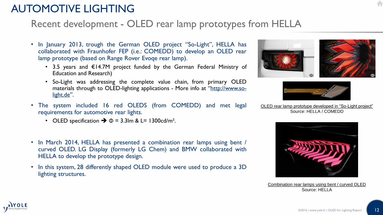
• In January 2013, trough the German OLED project “So-Light”, HELLA hascollaborated with Fraunhofer FEP (i.e.: COMEDD) to develop an OLED rearlamp prototype (based on Range Rover Evoqe rear lamp).
• 3.5 years and €14.7M project funded by the German Federal Ministry ofEducation and Research)
• So-Light was addressing the complete value chain, from primary OLEDmaterials through to OLED-lighting applications - More info at “http://www.so-light.de”.
• The system included 16 red OLEDS (from COMEDD) and met legalrequirements for automotive rear lights.
• OLED specification Φ = 3.3lm & L= 1300cd/m².
• In March 2014, HELLA has presented a combination rear lamps using bent /curved OLED. LG Display (formerly LG Chem) and BMW collaborated withHELLA to develop the prototype design.
• In this system, 28 differently shaped OLED module were used to produce a 3Dlighting structures.
Recent development - OLED rear lamp prototypes from HELLA
AUTOMOTIVE LIGHTING
OLED rear lamp prototype developed in “So-Light project”
Source: HELLA / COMEDD
Combination rear lamps using bent / curved OLED
Source: HELLA
©2016 | www.yole.fr | OLED for Lighting Report

13
Niche lighting applications could represent a business opportunity for OLED lighting panel of ~$XXM by 2021.
Take away
NICHE LIGHTING APPLICATIONS
• Niche lighting applications could be part of the spark required to trigger the OLED lighting market.
• As OLED represent still an emerging technology for lighting applications, such niches could help to develop theproduction scale momentum and create the marketing window demonstrating the advantages and possibilities of thetechnology for customers.
• However, to develop such strategy (i.e.: niche market strategy), investment will have to be done at the applicationlevel in order to identify applications for which OLED may provide an added value.
©2016 | www.yole.fr | OLED for Lighting Report

14
Lighting applications could represent a business opportunity for OLED device of ~$XXM by 2021.
TOTAL OLED LIGHTING MARKET OPPORTUNITY
©2016 | www.yole.fr | OLED for Lighting Report

15
• Most US, Japanese andEuropean companiesinvolved in OLEDs try tobenefit from thebooming Korean OLEDmarket (both for displaysand OLED lighting):
• Partnerships withleading Koreancompanies.
• Buildingmanufacturingfacilities in SouthKorea to be closerto the customers.
• Ease the access toKorean customersby acquisitions ofKorean companies.
• Selling technologyassets to theleading Koreanplayers.
South Korea = Centre of gravity for OLED business
OLED LIGHTING INDUSTRY
XX
XX
XX
Courtesy image: Wikipedia
OLED Plus
Supply Creation of Korean JV / subsidiary Acquisition
©2016 | www.yole.fr | OLED for Lighting Report

16
• The scheme below presents mainstream structures and materials used currently in commercial OLED lighting panel production:
OVERVIEW OF OLED STRUCTURES AND MATERIALS
Emitter
Organic
Materials
Phosphorescent
Fluorescent
For Dry Deposition
For Wet Deposition
Small-Molecules
Polymers
Rigid Glass
Ultra-thin Flexible GlassSubstrate
Glass
Metal Foil
Plastic Foil
OLED
Structure
Bottom-emitting OLED
Top-emitting OLED
Transparent OLED
Mainstream
Alternative
©2016 | www.yole.fr | OLED for Lighting Report
February 2016

17
PEDOT:PSS can be used both as anode and hole injection layer (HIL) between the anode and the OLED stack.
• Advantages:
• The HOMO level between the work function of ITO and the HOMO of other commonly used polymers Easierhole extraction.
• High transparency.
• XX.
• Improved adhesion of organic layers compared to direct deposition on ITO.
• It works as a protecting barrier to limit oxygen diffusion from anode.
• Drawbacks:
• PEDOT (poly(ethylenedioxythiophene)) Sensible to XX.
• Possibility of organic material deterioration due to the acid character of the PSS (Polystyrene Sulfonate of Sodium).
• Plextronics (US), acquired in 2014 by Solvay, developed and produces Plexcore® OC ink with a low acidity thatresults in low moisture absorbing films and thus longer OLED lifetime. The tunable nature of Plexcore® OC inkallows for control of final work function and conductivity of the HIL film.
• Plexcore® OC inks can also be used to form HIL films that are compatible with vapor deposited Small-MoleculeOLED (SMOLED) devices.
• Main suppliers of HIL materials:
• XX (...).
PEDOT:PSS AS HIL MATERIAL
Plexcore ® OC RG-1100 molecule
Source: Sigma-Aldrich
©2016 | www.yole.fr | OLED for Lighting Report

18
Emissive Layer (EL) usually consists of light-emitting dyes or dopants dispersed in a suitable host material.
Dopants (dyes) are used for:
• XX.
• XX.
HOST MATERIALS AND DOPANTS
ADNXX
CBPXX
MCP
XX
XX
XX
Host materials Dopant materialsWith the indication of emitted color
XX 2-methyl-8-
hydroxyquinolina
to lithium
XX
XX Ir(piq)3
©2016 | www.yole.fr | OLED for Lighting Report

19
Developing a cost-effective good barrier solution as an alternative to glass is a very challenging task.
• Today, the standard encapsulation solution is based on XX (excellent barrier), edge sealing using appropriate glue anddesiccant layer.
• Barriers based on XX have shown very good barrier properties, but the deposition of several inorganic layers makessuch barriers very costly.
• The high costs are mainly associated with costs of deposition of XX.
• There are several approaches to reduce the manufacturing costs:
• XX.This may result in reduced reliability and lifetime.
• Using alternative deposition technique for inorganic films, such as:
• XX
• XX
ENCAPSULATION - ALTERNATIVES TO A GLASS BARRIER
©2016 | www.yole.fr | OLED for Lighting Report

20
The manufacturing steps and techniques used are different for solution processable OLEDs and for OLEDs made by evaporation.
Manufacturing process flow for OLED lighting panel
OLED MANUFACTURING TECHNIQUES AND EQUIPMENT
Example of an OLED process flow for lighting applications: Three main phases of the OLED manufacturing
process with the relevant processing steps
Source: Yole Développement
LEP Layer(s)
Printing
Cathode
PrintingDrying
Encapsulation
LEP Ink
Formulation
Light out-
coupling
film
Evap.
HIL
Evap.
ETL
Evap.
EIL
Evap.
ELs
RGB
Evap.
HTL
Evap.
LiF
Evap.
Al
1. Substrate preparation
3. Encapsulation
2. Deposition of organic materials & cathode
Cathode Ink
Formulation
Drying
Anode (ITO)
deposition
Anode
patterning
Cleaning /
surface
pretreatment
Substrate
cleaning
LEP: Light Emitting Polymer, ITO: Indium-Tin-Oxide, HIL: Hole Injection Layer, HTL: Hole Transport Layer: EIL: Electron Injection Layer, EIL: Electron Injection Layer
All-Solution Processes
All-Evaporation Processes
Testing &
Sorting
©2016 | www.yole.fr | OLED for Lighting Report
February 2016

21
LG Display is leading the OLED lighting panel size, both for rigid and flexible panels.
Commercially available flexible OLED lighting panel is x5 smaller than the record-size rigid panel, and has lower performance.
The largest rigid and flexible OLED panels in 2016
OLED MANUFACTURING TECHNIQUES AND EQUIPMENT
Rigid OLED lighting panel Flexible OLED lighting panel
320mm x 320mm = 102,400mm2 406mm x 50mm = 20,300mm²
Rigid vs. Flexible record-size panel:• 5x bigger surface
• 20% higher efficacy
• Better CRI
• Better uniformity
• 2x higher lifetime
• 2x thicker
Record-size rigid and flexible OLED lighting panels produced by LG Display
Source: LG Chem / LG Display©2016 | www.yole.fr | OLED for Lighting Report

22
Often used for OLED manufacturing at XX scale.
BUT not adapted for XX.
Spin-coating
SOLUTION-BASED DEPOSITION TECHNIQUES
• Principle:
• Organic material in a liquid form is dropped onto a horizontally-placedsubstrate which is then spun at high speed (typically 1,000 to 4,000rpm).
• The material is spread on the substrate evenly by centrifugal force.
• During the subsequent heat treatment, a solid thin film is formed.
• Advantages:
• Simple technique and equipment.
Often used in laboratory for preparation of small-size samples.
• Challenges and drawbacks:
• Waste of material.
• A part of organic material is spun off the edges of the substrate.
• Not XX.
• Not XX.
• Necessity of a subsequent thermal step (drying).
Laboratory spin coater
Source: University of Bordeaux
Organic ink being dispensed on the
substrate prior to high-speed spinning
©2016 | www.yole.fr | OLED for Lighting Report

23
Roadmaps of many players are too optimistic / aggressive.
Industrial roadmaps
OLED MANUFACTURING COST
• OLED cost roadmaps presented by many manufacturers and organizations(e.g.: DoE…) involved in OLED development are very aggressive and seemnot realistic.
• Those aggressive targets are often based on:
• Unrealistic expectations regarding the transfer of OLED displaymanufacturing know-how to OLED lighting panels.
• Such unrealistic expectations were also made regarding the transfer of smallOLED display manufacturing know-how (i.e.: smartphone) to large OLEDdisplay panels (i.e.: TV). As a result, companies such as Samsung or LG havedelayed their roadmap toward OLED TVs.
• Overestimation of the time-to-market for new materials and technologysolutions.
• Underestimation of the complexity of the roll-to-roll process using solution-based materials (and promising very low costs).
• Overly optimistic expectations regarding OLED lighting market demand andunderestimation of the strong competition with existing lighting solutions(e.g.: LEDs…).
• Competition with LED is even more difficult as the LED technologydevelopment were in advanced toward industrial roadmap (performanceand cost).
• On the other hand, such aggressive roadmaps are also part of companies’strategies. Indeed, showing strong potential of development is a way to salethe technology.
Snapshot of LG Chem OLED roadmap
presented in 2014 / 2015 on LG Chem
website - Maximum efficiency of company’s
OLED panel is currently of 60lm/W
©2016 | www.yole.fr | OLED for Lighting Report

24
• Financing for OLED lighting R&D activities can be obtained from different sources:
• Public institutions: U.S. Department of Energy, European Commission, BMBF (…).
• Regions: North Rhine-Westphalia in Germany (…).
• Industrial companies (via partnerships, Joint Development Programs, JointVentures…) (…).
• Main institutions / organizations are described below:
Note: Recent OLED lighting R&D projects supported by these institutions / organizations are listed in appendix.
Main financing institutions / organizations for OLED lighting R&D Activities
OLED ROADMAP AND R&D ACTIVITIES
Name Full name Country Supported activities Website
DOE, EERE
U.S. Department of Energy
Energy Efficiency and
Renewable Energy
USA
• A major DOE objective in funding OLED projects is to develop, establish, and/or maintain
the OLED technology and manufacturing base within the U.S., which will create jobs and
promote the nation's role as a leader in the field.
http://www.eere.energy.gov/
EC European Commission EU
• Study of processes in OLEDs.
• Development of new materials, structures, device architectures and manufacturing
processes.
http://cordis.europa.eu/
BMBF
Bundesministerium für
Bildung und Forschung
(Federal Ministry of
Education and Research)
Germany
• New component structures, enabling an improved performance of OLED devices (e.g.:
white OLEDs with efficiencies of more than 100lm/W at a brightness of 3000cd/m² and a
good color rendering index (CRI > 80)).
• Concepts to improve light extraction or to avoid loss mechanisms.
• New OLED emitter, in particular in the blue spectral range.
• Materials for efficient charge carrier transport.
• Up-scaling of synthesis processes of OLED materials.
• Research and demonstration of new lighting concepts based on OLEDs.
http://www.bmbf.de/
NEDO
New Energy and Industrial
Technology Development
Organization
Japan• Promoting research and deployment of renewable energy, environmental and industrial
technologies, including energy efficient OLED.http://www.nedo.go.jp/
©2016 | www.yole.fr | OLED for Lighting Report

From Technologies to Market
Presentation of Yole Développement
With Focus on Sapphire LED, OLED and Display /
Lighting Activities
Corporate Presentation
From Technologies to Market


27
MEMS &
Sensors
LED
Compound
Semi.
Imaging Photonics
MedTech
Manufacturing
Advanced Packaging
Batteries / Energy
Management
Power
Electronics
FIELDS OF EXPERTISE
Yole Développement’s 30 analysts operate in the following areas
©2016 | www.yole.fr | OLED for Lighting Report

28
4 BUSINESS MODELS
o Consulting and Analysis
• Market data & research, marketing analysis
• Technology analysis
• Strategy consulting
• Reverse engineering & costing
• Patent analysis
www.yole.fr
o Reports
• Market & Technology reports
• Patent Investigation and patent infringement riskanalysis
• Teardowns & Reverse Costing Analysis
• Cost Simulation Tool
www.i-Micronews.com/reports
o Financial services
• M&A (buying and selling)
• Due diligence
• Fundraising
• Maturation of companies
• IP portfolio management & optimization
www.yolefinance.com
www.bmorpho.com
o Media
• i-Micronews.com website
• @Micronews e-newsletter
• Communication & webcast services
• Events
www.i-Micronews.com
©2016 | www.yole.fr | OLED for Lighting Report

29
A GROUP OF COMPANIES
Market,
technology and
strategy
consulting
www.yole.fr
M&A operations
Due diligences
www.yolefinance.com
Innovation and business maker
www.bmorpho.com
Manufacturing costs analysis
Teardown and reverse engineering
Cost simulation tools
www.systemplus.fr
IP analysis
Patent assessment
www.knowmade.fr
©2016 | www.yole.fr | OLED for Lighting Report

30
OUR 2016 REPORTS PLANNINGo MEMS & SENSORS
− Gas Sensors and Combos 2016
− Status of the MEMS Industry 2016*
− Sensors for Cellphones and Tablets 2016
− Market and Technology Trends of Inkjet Printheads: Towards New Printing Opportunities
2016…
− Sensors for Biometry and Recognition 2016
− Finger Print Sensors Market and Technologies 2016
− 3D Imaging & Sensing 2016**
− Silicon Photonics 2016
− Emerging Non Volatile Memories 2016*
− AlN Thin Film Markets and Applications 2016
o IMAGING & OPTOELECTRONICS
− Status of the CMOS Image Sensor Industry 2016*
− Uncooled Infrared Imaging Technology & Market Trends 2016*
− Imaging Technologies for Automotive 2016
− Sensors for Drones & Consumer Robots 2016
− 3D Imaging & Sensing 2016**
− Silicon Photonics 2016
o MEDTECH
− BioMEMS 2016
− Point of Need Testing 2016: Application of Microfluidic Technologies
o ADVANCED PACKAGING
− FanOut WLP: Technology Trends and Business Update 2016*
− Embedded Die Packaging: Technology and Markets Trends 2016*
− 2.5D & 3D IC Business Update 2016
− Status of the Advanced Packaging Industry 2016*
− Advanced Packaging for Wearables and Mobile Applications 2016
− Advanced Packaging in Emerging Markets: China 2016
− Supply Chain Readiness for Panel Manufacturing in Packaging 2016
o MANUFACTURING
− Inspection and Metrology Technology and Applications Trends in Advanced Packaging 2016**
− Emerging Materials for Advanced Packaging 2016
− Deposition Technologies Equipment & Materials 2016
− Thinning & Dicing Equipment for Advanced Packaging, MEMS, Photovoltaics, LED, CMOS 2016
o COMPOUND SEMICONDUCTORS
− SiC Modules, Devices and Substrates for Power Electronics 2016*
− GaN Modules, Devices and Substrates for Power Electronics 2016*
− Sapphire Applications & Market 2016: from LED to Consumer Electronics*
− RF GaN Technology and Market Analysis 2016
o LED
− Sapphire Applications and Market 2016: From LED to Consumer Electronics*
− LED Packaging 2016
− Microdisplays and MicroLEDs
− UV LED Technology, Manufacturing and Applications Trends 2016*
− OLED for Lighting 2016
− LED in Automotive Lighting 2016
o POWER ELECTRONICS
− Power Electronics in Electric and Hybrid Vehicles 2016
− Status of Power Electronics Industry 2016*
− Passive Components Technologies and Market Trends for Power Electronics 2016
− SiC Modules, Devices and Substrates for Power Electronics 2016*
− GaN Modules, Devices and Substrates for Power Electronics 2016*
− Inverter Technologies Trends & Market Expectations 2016
− Power Electronics for Renewable Energy 2016
− Thermal Management for LED and Power 2016
− RF GaN Technology and Market Analysis 2016
o BATTERY
− Market Trends and Technologies in Battery Pack and Assembly 2016
− Innovative and Emerging Technologies in Energy Storage Market 2016
**To be confirmed
Patent Analysis by Knowmade and Teardown & Reverse Costing by System Plus Consulting are available on
www.i-micronews.com
©2016 | www.yole.fr | OLED for Lighting Report

31
OUR 2015 PUBLISHED REPORTS LIST
o MEMS & SENSORS
− Sensors and Data Management for Autonomous Vehicles
− Sensors for Wearable Electronics And Mobile Healthcare
− Status of the MEMS Industry
− Uncooled Infrared Imaging Technology & Market Trends
− Infrared Detector Technology & Market Trends
− High-End Gyroscopes, Accelerometers and IMUs for Defense, Aerospace & Industrial
− Emerging Non Volatile Memory (NVM) Technology & Market Trends
o IMAGING & OPTOELECTRONICS
− Camera Module Industry
− Uncooled Infrared Imaging Technology & Market Trends
− Status of the CMOS Image Sensors
− Infrared Detector Technology & Market Trends
o MEDTECH
− Sample Preparation Automation Through Emerging Microfluidic Technologies
− 2015 Microfluidic Applications in the Pharmaceutical, Life Sciences, In-Vitro Diagnostic, and
Medical Device Markets
− Sensors for Wearable Electronics And Mobile Healthcare
o COMPOUND SEMICONDUCTORS
− Sapphire Applications & Market 2015: from LED to Consumer Electronics
− SiC, GaN, and other Wide Band Gap (WBG) materials for power electronics applications
− GaN and SiC Devices for Power Electronics Applications
o LED
− LED Lighting Module Technology, Industry and Market Trends 2015
− UV LED - Technology, Manufacturing and Application Trends
− Phosphors & Quantum Dots 2015: LED Downconverters for Lighting & Displays
− Sapphire Applications & Market 2015: from LED to Consumer Electronics
o POWER ELECTRONICS
− Power Packaging Technology Trends and Market Expectations
− Energy Management for Smart Grid, Cities and Buildings: Opportunities for Battery
Electricity Storage Solutions
− Status of Chinese Power Electronics Industry
− New Technologies and Architectures for Efficient Data Center
− IGBT Market and Technology Trends
− Status of Power Electronics Industry
− SiC, GaN, and other Wide Band Gap (WBG) materials for power electronics applications
− GaN and SiC Devices for Power Electronics Applications
o ADVANCED PACKAGING
− Status of the Advanced Packaging Industry
− Supply Chain Readiness for Panel Manufacturing in Packaging
− Fan-in Wafer Level Packaging: Market and Technology Trends
− Flip Chip: Technologies and Markets Trends
− Fan-Out and Embedded Die: Technologies & Market Trends
o MANUFACTURING
− Photolithography Equipment and Materials for Advanced Packaging, MEMS and LED
Applications
− Emerging Non Volatile Memory (NVM) Technology & Market Trends
Patent Analysis by Knowmade and Teardown & Reverse Costing by System Plus Consulting are
available on www.i-micronews.com
©2016 | www.yole.fr | OLED for Lighting Report

32
CONTACT INFORMATION
Follow us on
• Consulting and Specific Analysis
• North America: Steve LaFerriere, Director of Northern America Business DevelopmentEmail: [email protected]
• Japan & Asia: Takashi Onozawa, Representative Director, Yole KKEmail: [email protected]
• RoW: Jean-Christophe Eloy, CEO & President, Yole DéveloppementEmail [email protected]
• Report business
• North America: Steve LaFerriere, Director of Northern America Business DevelopmentEmail: [email protected]
• Europe: Fayçal El Khamassi, Headquarter Sales Coordination & Customer Service Email: [email protected]
• Japan & Asia: Takashi Onozawa, Representative Director, Yole KK.Email: [email protected]
• Korea: Hailey Yang, Business Development Manager, Korean OfficeEmail: [email protected]
• Taiwan: Mavis Wang, Business Development DirectorEmail: [email protected]
• Financial services
• Jean-Christophe Eloy, CEO & PresidentEmail: [email protected]
• General
• Email: [email protected]
©2016 | www.yole.fr | OLED for Lighting Report

33
About Sapphire, LED / OLED and Display / Lighting Activities

34
We are active throughout the value chain: from substrates to systems! And we interact with industrial / R&D players from each level!
Yole is active throughout the value chain (Example of LED and Sapphire activities)
FOCUS ON SAPPHIRE, LED / OLED AND DISPLAY / LIGHTING ACTIVITIES
Substrate
SiC / Sapphire / Silicon /
Bulk GaN / Engineered
substrates
LED epi-
wafer
Mesa LED, Flip Chip LED,
Vertical LED structures
LED dies-
on-wafer
LED dies
Front-end Level 0 - Epitaxy• Nucleation layer
• n-type layer
• Active layers (MQW)
• p-type layer
Back-End Level 0 - Packaging• Substrate separation & Bonding
• Die singulation
• Testing & Binning
LED systems and applications
Front-end Level 1 - Device Production• Inspection
• Masking / Lithography
• Etching
• Metallization / Contacts / Mirrors
Back-End level 1 - Packaging• Die Attach & Interconnections
• Phosphors
• Encapsulation & Optics
• Testing & Binning
Packaged LEDs
Module Packaging• Substrates (PCB)
• Encapsulation & Optics
• Heatsink
• Testing & Binning
LED modules

35
FOCUS ON SAPPHIRE, LED / OLED AND DISPLAY / LIGHTING ACTIVITIES
Insights on Forecast Methodology
“What’s Behind the Crystal Ball?”
Only analysts that follow the industry on a daily basis (trough interviews and developed market modeling tools based on discussions with key players of the industry.
APPLICATION
Forecast of standard
product market volume
(unit)Ex.: Smartphone, TVs, lamps (…)
Definition of functions using
LEDsEx.: “Flash vs. Keypad” for
smartphone (…)
Definition of technical
requirementsEx.: Efficacy, size (…)
Definition of LED
penetration rate and
competitiveness with
alternative technologiesEx.: “OLED vs. LED” in smartphone
(…)
Forecast of LED market volume (unit)Split by application, power type (low vs. medium vs. high
power), package type (single vs. multi-die…) (… )
Definition of LED
ASPPer power type, packaged
type (…)
Forecast of LED market size ($)Split by application, power type, package type
(… )
Definition of manufacturing flows for
front-end and packaging (process,
technologies, materials, yields…)Split by application, power type, package type (…)
Forecast of LED manufacturing
equipment and material markets
(unit and $)Ex.: Phosphors, encapsulant, dicing equipment
Definition of LED die
surface (mm²)
Definition of substrate die surface (mm²)
and epiwafer volume (unit)Split by type of substrate (…)
Forecast of LED substrate
markets (unit and $)Split by type of substrate (…)
Definition of sale
levels of key
manufacturers ($)Ex: LED, packaging
materials, epitaxy
materials, manufacturing
equipment, MOCVD
reactor, substrate (…)
System Plus Consulting
expertise in reverse
costing / reverse
engineering

36
A team based on persons having complementary skills and expertise.
About Yole’s Analyst Team
FOCUS ON SAPPHIRE, LED / OLED AND DISPLAY / LIGHTING ACTIVITIES
Pierrick BOULAY - Market & Technology Analyst
Pierrick BOULAY holds a master degree in Electronics from ESEO (France). He works as Market and Technology Analyst
in the fields of LED, OLED and Lighting Systems to carry out technical, economic and marketing analysis. He has experience
in both LED lighting (general lighting, automotive lighting…) and OLED lighting. In the past, he has mostly worked in R&D
department for LED lighting applications.
Pars MUKISH - Business Unit Manager
Pars MUKISH holds a master degree in Materials Science & Polymers (ITECH - France) and a master degree in Innovation
& Technology Management (EM Lyon - France). Since 2015, Pars MUKISH has taken on responsibility for developing LED,
OLED and Sapphire activities as Business Unit Manager at Yole Développement. Previously, he has worked as Marketing
Analyst and Techno-Economic Analyst for several years at the CEA (French Research Center).
Dr. Eric VIREY - Senior Market & Technology Analyst
Eric VIREY holds a Ph-D in Optoelectronics from the National Polytechnic Institute of Grenoble (INPG - France). He
works as Market and Technology Analyst in the fields of Sapphire, LED / OLED and Display. In the last 12 years, he has held
various R&D, engineering, manufacturing and marketing positions with Saint-Gobain. Most recently, he was Market Manager at
Saint-Gobain Crystals, in charge of Sapphire and Optoelectronic products.
Dr. Milan ROSINA - Senior Market & Technology Analyst
Milan ROSINA holds a Ph-D in Optoelectronics from the National Polytechnic Institute of Grenoble (INPG - France). He
works as Market and Technology Analyst in the fields of Energy Conversion, LED / OLED and Emerging Materials. Before
joining Yole Développement, he has worked as research scientist and project manager in PV, microelectronics and LED
industries. He has more than 15 year experience with prominent research institutions and a utility company.
37
A collection of more than 15 reports on Sapphire, LED, OLED, Display and Lighting.
Report collection
FOCUS ON SAPPHIRE, LED / OLED AND DISPLAY / LIGHTING ACTIVITIES
Already published -Yole Développement:
• Status of the LED Industry
• LED in Road and Street Lighting
• LED Front End ManufacturingTrends
• LED Front End Equipment Market trends
• GaN-on-SiTechnology and Market
• Phosphors & QDs - Market and Technology Landscape
• LED Module Technologies
• Phosphors & QDs - IP Landscape
From System Plus Consulting:
• LED CoSim+ & Reverse Engineering / Reverse Costing reports
2016 Publication -To be published -Yole Développement :
• OLED For Lighting (Q1 - 2016)
• Automotive Lighting (Q1 - 2016)
• LED Packaging (Q2 - 2016)
• Sapphire (Q2 / Q3 - 2016)
• UV LED (Q3 - 2016)
• MicroDisplays and MicroLEDs (Q3 - 2016)
Our reports are unmatched in quality and technology depth and typically include:
• Technology trends and evolution: costs, barriers, roadmaps (…).
• Supply & value chain analysis: business models, relationships, value flows (…).
• In-depth analysis of applications and market drivers: challenges, inflection points (…).
• Market data ($, units, wafer starts…)

ORDER FORMOLED for Lighting - Technology, Industry and Market Trends
SHIPPING CONTACT
First Name:
Email:
Last Name:
Phone:
PAYMENT
BY CREDIT CARD Visa Mastercard Amex
Name of the Card Holder:
Credit Card Number:
Card Verification Value (3 digits except AMEX: 4 digits):
Expiration date:
BY BANK TRANSFERBANK INFO: HSBC, 1 place de la Bourse, F-69002 Lyon, France, Bank code: 30056, Branch code: 00170Account No: 0170 200 1565 87, SWIFT or BIC code: CCFRFRPP, IBAN: FR76 3005 6001 7001 7020 0156 587
RETURN ORDER BY • FAX: +33 (0)472 83 01 83• MAIL: YOLE DÉVELOPPEMENT, Le Quartz,
75 Cours Emile Zola, 69100 Villeurbanne/Lyon - France
SALES CONTACTS • North America: Steve Laferriere - [email protected]• Japan & Asia: Takashi Onozawa - [email protected]• Greater China: Mavis Wang - [email protected]• Europe & RoW: Fayçal Khamassi - [email protected]• Korea: Hailey Yang - [email protected]• General: [email protected]
(1) Our Terms and Conditions of Sale are available at www.yole.fr/Terms_and_Conditions_of_Sale.aspx The present document is valid 24 months after its publishing date: March 1st, 2016
/
ABOUT YOLE DEVELOPPEMENT
BILL TO
Name (Mr/Ms/Dr/Pr):
Job Title:
Company:
Address:
City:
State:
Postcode/Zip:
Country*:
*VAT ID Number for EU members:
Tel:
Email:
Date:
PRODUCT ORDER
Please enter my order for above named report: One user license*: Euro 5,490 Multi user license: Euro 6,490- The report will be ready for delivery from March 1st, 2016- For price in dollars, please use the day’s exchange rate. All reports are
delivered electronically at payment reception. For French customers, add 20% for VAT
I hereby accept Yole Développement’s Terms and Conditions of Sale(1)
Signature:
*One user license means only one person at the company can use the report.
Founded in 1998, Yole Développement has grown to become a group of companies providing marketing, technology and strategy consulting, media in addition to corporate finance services. With a strong focus on emerging applications using silicon and/or micro manufacturing (technology or process), Yole Développement group has expanded to include more than 50 associates worldwide covering MEMS, Compound Semiconductors, LED, Image Sensors, Optoelectronics, Microfluidics & Medical, Photovoltaics, Advanced Packaging, Manufacturing, Nanomaterials and Power Electronics. The group supports industrial companies, investors and R&D organizations worldwide to help them understand markets and follow technology trends to develop their business.
MEDIA & EVENTS• i-Micronews.com, online disruptive technologies website• @Micronews, weekly e-newsletter• Communication & webcasts services• Events: Yole Seminars, Market Briefings…More information on www.i-micronews.com
CONTACTSFor more information about :• Consulting Services: Jean-Christophe Eloy ([email protected])• Financial Services: Jean-Christophe Eloy ([email protected])• Report Business: Fayçal Khamassi ([email protected])• Press relations: Sandrine Leroy ([email protected])
CONSULTING• Market data & research, marketing analysis• Technology analysis• Reverse engineering & costing services• Strategy consulting• Patent analysisMore information on www.yole.fr
REPORTS• Collection of technology & market reports• Manufacturing cost simulation tools• Component reverse engineering & costing
analysis• Patent investigationMore information on www.i-micronews.com/reports
FINANCIAL SERVICES• Mergers & Acquisitions• Due diligence• FundraisingMore information on Jean-Christophe Eloy ([email protected])

Definitions: “Acceptance”: Action by which the Buyer accepts the terms and conditions of sale in their entirety. It is done by signing the purchase order which mentions “I hereby accept Yole’s Terms and Conditions of Sale”.
“Buyer”: Any business user (i.e. any person acting in the course of its business activities, for its business needs) entering into the following general conditions to the exclusion of consumers acting in their personal interests.
“Contracting Parties” or “Parties”: The Seller on the one hand and the Buyer on the other hand.
“Intellectual Property Rights” (“IPR”) means any rights held by the Seller in its Products, including any patents, trademarks, registered models, designs, copyrights, inventions, commercial secrets and know-how, technical information, company or trading names and any other intellectual property rights or similar in any part of the world, notwithstanding the fact that they have been registered or not and including any pending registration of one of the above mentioned rights.
“License”: For the reports and databases, 3 different licenses are proposed. The buyer has to choose one license:• One user license: one person at the company can use the report.• Multi-user license: the report can be used by unlimited users
within the company. Subsidiaries and Joint-Ventures are not included.
• Corporate license: purchased under “Annual Subscription” program, the report can be used by unlimited users within the company. Joint-Ventures are not included.
“Products”: Depending on the purchase order, reports or database on MEMS, CSC, Optics/MOEMS, Nano, bio… to be bought either on a unit basis or as an annual subscription. (i.e. subscription for a period of 12 calendar months). The annual subscription to a package (i.e. a global discount based on the number of reports that the Buyer orders or accesses via the service, a global search service on line on I-micronews and a consulting approach), is defined in the order. Reports are established in PowerPoint and delivered on a PDF format and the database may include Excel files.
“Seller”: Based in Lyon (France headquarters), Yole Développement is a market research and business development consultancy company, facilitating market access for advanced technology industrial projects. With more than 20 market analysts, Yole works worldwide with the key industrial companies, R&D institutes and investors to help them understand the markets and technology trends.
1. SCOPE 1.1 The Contracting Parties undertake to observe the following
general conditions when agreed by the Buyer and the Seller. ANY ADDITIONAL, DIFFERENT, OR CONFLICTING TERMS AND CONDITIONS IN ANY OTHER DOCUMENTS ISSUED BY THE BUYER AT ANY TIME ARE HEREBY OBJECTED TO BY THE SELLER, SHALL BE WHOLLY INAPPLICABLE TO ANY SALE MADE HEREUNDER AND SHALL NOT BE BINDING IN ANY WAY ON THE SELLER.
1.2 This agreement becomes valid and enforceable between the Contracting Parties after clear and non-equivocal consent by any duly authorized person representing the Buyer. For these purposes, the Buyer accepts these conditions of sales when signing the purchase order which mentions “I hereby accept Yole’s Terms and Conditions of Sale”. This results in acceptance by the Buyer.
1.3 Orders are deemed to be accepted only upon written acceptance and confirmation by the Seller, within [7 days] from the date of order, to be sent either by email or to the Buyer’s address. In the absence of any confirmation in writing, orders shall be deemed to have been accepted.
2. MAILING OF THE PRODUCTS 2.1 Products are sent by email to the Buyer:
• within [1] month from the order for Products already released; or • within a reasonable time for Products ordered prior to their effective release. In this case, the Seller shall use its best endeavours to inform the Buyer of an indicative release date and the evolution of the work in progress.
2.2 Some weeks prior to the release date the Seller can propose a pre-release discount to the Buyer The Seller shall by no means be responsible for any delay in respect of article 2.2 above, and including incases where a new event or access to new contradictory information would require for the analyst extra time to compute or compare the data in order to enable the Seller to deliver a high quality Products.
2.3 The mailing of the Product will occur only upon payment by the Buyer, in accordance with the conditions contained in article 3.
2.4. The mailing is operated through electronic means either by email via the sales department or automatically online via an email/password. If the Product’s electronic delivery format is defective, the Seller undertakes to replace it at no charge to the Buyer provided that it is informed of the defective formatting within 90 days from the date of the original download or receipt of the Product.
2.5 The person receiving the Products on behalf of the Buyer shall immediately verify the quality of the Products and their conformity to the order. Any claim for apparent defects or for non-conformity shall be sent in writing to the Seller within 8 days of receipt of the Products. For this purpose, the Buyer agrees to produce sufficient evidence of such defects. .
2.6 No return of Products shall be accepted without prior information to the Seller, even in case of delayed delivery. Any Product returned to the Seller without providing prior information to the Seller as required under article 2.5 shall remain at the Buyer’s risk.
3. PRICE, INVOICING AND PAYMENT 3.1 Prices are given in the orders corresponding to each Product
sold on a unit basis or corresponding to annual subscriptions. They are expressed to be inclusive of all taxes. The prices may be reevaluated from time to time. The effective price is deemed to be the one applicable at the time of the order.
3.2 Yole may offer a pre release discount for the companies willing to acquire in the future the specific report and agreeing on the fact that the report may be release later than the anticipated release date. In exchange to this uncertainty, the company will get a discount that can vary from 15% to 10%.
3.3 Payments due by the Buyer shall be sent by cheque payable to Yole Développement, credit card or by electronic transfer to the following account: HSBC, 1 place de la Bourse 69002 Lyon France Bank code: 30056 Branch code: 00170 Account n°: 0170 200 1565 87BIC or SWIFT code: CCFRFRPP IBAN: FR76 3005 6001 7001 7020 0156 587
To ensure the payments, the Seller reserves the right to request down payments from the Buyer. In this case, the need of down payments will be mentioned on the order. 3.4 Payment is due by the Buyer to the Seller within 30 days
from invoice date, except in the case of a particular written agreement. If the Buyer fails to pay within this time and fails to contact the Seller, the latter shall be entitled to invoice interest in arrears based on the annual rate Refi of the «BCE» + 7 points, in accordance with article L. 441-6 of the French Commercial Code. Our publications (report, database, tool...) are delivered only after reception of the payment.
3.5 In the event of termination of the contract, or of misconduct, during the contract, the Seller will have the right to invoice at the stage in progress, and to take legal action for damages.
4. LIABILITIES 4.1 The Buyer or any other individual or legal person acting on
its behalf, being a business user buying the Products for its business activities, shall be solely responsible for choosing the Products and for the use and interpretations he makes of the documents it purchases, of the results he obtains, and of the advice and acts it deduces thereof.
4.2 The Seller shall only be liable for (i) direct and (ii) foreseeable pecuniary loss, caused by the Products or arising from a material breach of this agreement
4.3 In no event shall the Seller be liable for: a) damages of any kind, including without limitation, incidental or consequential damages (including, but not limited to, damages for loss of profits, business interruption and loss of programs or information) arising out of the use of or inability to use the Seller’s website or the Products, or any information provided on the website, or in the Products; b) any claim attributable to errors, omissions or other inaccuracies in the Product or interpretations thereof.
4.4 All the information contained in the Products has been obtained from sources believed to be reliable. The Seller does not warrant the accuracy, completeness adequacy or reliability of such information, which cannot be guaranteed to be free from errors.
4.5 All the Products that the Seller sells may, upon prior notice to the Buyer from time to time be modified by or substituted with similar Products meeting the needs of the Buyer. This modification shall not lead to the liability of the Seller, provided that the Seller ensures the substituted Product is similar to the Product initially ordered.
4.6 In the case where, after inspection, it is acknowledged that the Products contain defects, the Seller undertakes to replace the defective products as far as the supplies allow and without indemnities or compensation of any kind for labor costs, delays, loss caused or any other reason. The replacement is guaranteed for a maximum of two months starting from the delivery date. Any replacement is excluded for any event as set out in article 5 below.
4.7 The deadlines that the Seller is asked to state for the mailing of the Products are given for information only and are not guaranteed. If such deadlines are not met, it shall not lead to any damages or cancellation of the orders, except for non acceptable delays exceeding [4] months from the stated deadline, without information from the Seller. In such case only, the Buyer shall be entitled to ask for a reimbursement of its first down payment to the exclusion of any further damages.
4.8 The Seller does not make any warranties, express or implied, including, without limitation, those of sale ability and fitness for a particular purpose, with respect to the Products. Although the Seller shall take reasonable steps to screen Products for infection of viruses, worms, Trojan horses or other codes containing contaminating or destructive properties before making the Products available, the Seller cannot guarantee that any Product will be free from infection.
5. FORCE MAJEURE The Seller shall not be liable for any delay in performance directly or indirectly caused by or resulting from acts of nature, fire, flood, accident, riot, war, government intervention, embargoes, strikes, labor difficulties, equipment failure, late deliveries by suppliers or other difficulties which are beyond the control, and not the fault of the Seller.
6. PROTECTION OF THE SELLER’S IPR 6.1 All the IPR attached to the Products are and remain the
property of the Seller and are protected under French and international copyright law and conventions.
6.2 The Buyer agreed not to disclose, copy, reproduce, redistribute, resell or publish the Product, or any part of it to any other party other than employees of its company. The Buyer shall have the right to use the Products solely for its own internal information purposes. In particular, the Buyer shall therefore not use the Product for purposes such as: • Information storage and retrieval systems; • Recordings and re-transmittals over any network (including
any local area network); • Use in any timesharing, service bureau, bulletin board or
similar arrangement or public display; • Posting any Product to any other online service (including
bulletin boards or the Internet);• Licensing, leasing, selling, offering for sale or assigning the
Product. 6.3 The Buyer shall be solely responsible towards the Seller of
all infringements of this obligation, whether this infringement comes from its employees or any person to whom the Buyer has sent the Products and shall personally take care of any related proceedings, and the Buyer shall bear related financial consequences in their entirety.
6.4 The Buyer shall define within its company point of contact for the needs of the contract. This person will be the recipient of each new report in PDF format. This person shall also be responsible for respect of the copyrights and will guaranty that the Products are not disseminated out of the company.
6.5 In the context of annual subscriptions, the person of contact shall decide who within the Buyer, shall be entitled to access on line the reports on I-micronews.com. In this respect, the Seller will give the Buyer a maximum of 10 password, unless the multiple sites organization of the Buyer requires more passwords. The Seller reserves the right to check from time to time the correct use of this password.
6.6 In the case of a multisite, multi license, only the employee of the buyer can access the report or the employee of the companies in which the buyer have 100% shares. As a matter of fact the investor of a company, the joint venture done with a third party etc..cannot access the report and should pay a full license price.
7. TERMINATION 7.1 If the Buyer cancels the order in whole or in part or postpones
the date of mailing, the Buyer shall indemnify the Seller for the entire costs that have been incurred as at the date of notification by the Buyer of such delay or cancellation. This may also apply for any other direct or indirect consequential loss that may be borne by the Seller, following this decision.
7.2 In the event of breach by one Party under these conditions or the order, the non-breaching Party may send a notification to the other by recorded delivery letter upon which, after a period of thirty (30) days without solving the problem, the non-breaching Party shall be entitled to terminate all the pending orders, without being liable for any compensation.
8. MISCELLANEOUS All the provisions of these Terms and Conditions are for the benefit of the Seller itself, but also for its licensors, employees and agents. Each of them is entitled to assert and enforce those provisions against the Buyer. Any notices under these Terms and Conditions shall be given in writing. They shall be effective upon receipt by the other Party. The Seller may, from time to time, update these Terms and Conditions and the Buyer, is deemed to have accepted the latest version of these terms and conditions, provided they have been communicated to him in due time.
9. GOVERNING LAW AND JURISDICTION 9.1 Any dispute arising out or linked to these Terms and
Conditions or to any contract (orders) entered into in application of these Terms and Conditions shall be settled by the French Commercial Courts of Lyon, which shall have exclusive jurisdiction upon such issues.
9.2 French law shall govern the relation between the Buyer and the Seller, in accordance with these Terms and Conditions.
TERMS AND CONDITIONS OF SALES