of the fix and the start of discharge can thereby be...
TRANSCRIPT

~ 1 ~
Triggering and measurement circuits needed to fire a coil gun
I envision a coil gun having several coils. Three different types of circuits will be needed. The first coil
in the gun will be activated when the user manually pushes a pushbutton switch. That circuit starts the
discharge of the capacitor which powers the first coil. Assuming that the slug is always positioned in the
right place before the gun is fired, the first circuit merely needs to start current flowing through the first
coil. A separate type of circuit will be needed to control the timing of the second and following coils.
These circuits will have to know, or estimate, the slug's location to determine the right moment at which
to start current flowing through the subsequent coils. Finally, a third circuit, with sensors located near the
end of the barrel, will be used to determine the slug's final speed.
Let me explain why I have chosen to control the timing of the second and subsequent coils by detecting
the slug's location. There is another way to control their timing, which I have rejected. The other way is
to use timers, one for each coil, which begin counting when the gun is fired. Yes, that can be done and, in
fact, would be easier to implement. Even the route I did choose, which is based on detecting the slug's
location, does require timing a short delay. The difference between the two design choices is not whether
or not a timed delay should be used, but rather how long of a delay can be permitted. If you are reading
this, you already know that the effectiveness of a particular coil is highly dependent on the slug's location
with respect to the coil when the capacitor starts its discharge. An incorrect starting location, off by just a
few millimeters, can seriously degrade performance. Uncertainty about the slug's location increases as
the slug travels further and further down the barrel. Making things worse is the fact that successive
firings of the gun will not be identical. There will be differences in temperature and residual
magnetization, components will degrade, and so on. I believe that the best way to overcome the
uncertainty is to get a "fix" on the slug's location just before it enters a coil. The delay between the time
of the "fix" and the start of discharge can thereby be reduced to the order of 100μs or less, from the 10ms
it takes for the slug to reach one of the later coils.
Let me also explain why I have chosen to build a speed-measurement circuit right into the gun. Some
kind of performance sensor must be available in order to "debug" the individual coils. It is possible to
adjust the capacitors' starting voltages and the slug's starting locations (by adjusting the delay after the
"fix") for each coil. But these adjustments can only be made sensibly if there is some way to measure the
effect of changing the starting conditions.
In an earlier paper titled A triggering circuit for the high-power SCR in a coil gun, I described a circuit
which starts the release of energy from a charged capacitor. The entry point of that circuit is a standard
2-input NAND gate. One of the two input lines comes from a "Ready" circuit, and goes high once
everything is ready for firing. The second input must be a short positive pulse. Its rising edge will cause
the NAND gate's output voltage to go low, thus starting the capacitor's discharge. The two triggering
circuits I describe below have been designed so their output is a short positive pulse which can be
delivered directly to a NAND gate. The output from the third circuit, the speed measurement circuit, is a
numeric LED display.
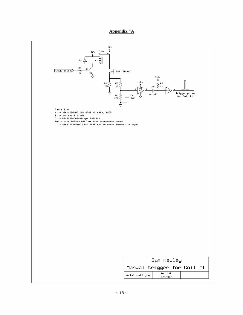
Circuit #1 - The manual trigger for the first coil
The first coil will be triggered manually, using a pushbutton switch. The schematic diagram for this
circuit is shown below. The pushbutton switch SW1 is labeled "Shoot" in the schematic. It is a single-
pole single-throw off-momentary pushbutton. It will do nothing unless the K1 relay is closed. K1's
contacts are normally open and prevent the 12V power supply voltage from reaching the pushbutton
switch until the system is ready. I will explain in a subsequent paper what constitutes readiness and how
the (high) Ready voltage is generated. It is enough for now to observe that a high Ready voltage will

~ 2 ~
cause current to flow through Q1's base resistor R1. Transistor Q1 will be driven into saturation and the
current which flows into Q1's collector through the coil of the relay will cause its contacts to close.
Transistor Q1 is a general purpose 2N2222A npn transistor. When its base-emitter junction is forward
biased, the voltage drop from Q1's base terminal to its emitter terminal will be about 0.7V, which is
typical for a forward-biased p-n junction. If the Ready voltage is high, which is to say 12V, then the
voltage drop over base resistor R1 will be 11.3V. The current flowing through R1 will be (using Ohm's
Law) I = V R = 11.3 1K = 11.3mA. If (note that this is an assumption) transistor Q1 is operating in its
linear region, then its collector current will be a factor of 75 or so greater than the base current. (This
factor is called the d.c. current gain and it is identified in the datasheet by the symbol HFE.) That means
that the current flowing into Q1's collector terminal would be 11.3mA 75 = 850mA. Now, then, the
datasheet for K1 states that the coil's nominal resistance is 1000Ω. If 850mA is flowing through that
resistance, then the voltage drop will be (using Ohm's Law once again) V = I R = 850mA 1K =
850 Volts. That is just not possible. What's wrong is that we made the wrong assumption. So, let's make
a different assumption. Let's assume (this is also an assumption) that transistor Q1 is operating in its
saturation mode. In saturation, all three terminals of the transistor are shorted out to each other. (The
short is not perfect, of course. Sometimes it is necessary to be a little bit more precise and take into
account the 0.2V drop or so that will exist between the collector terminal and the emitter terminal. We do
not need to do that here.) If the terminals are shorted, then K1's coil will be exposed to the power supply's
full 12 Volts, and the current which will flow through the coil will be I = V R = 12 1K = 12mA. The
current flowing into Q1's base terminal should be one-seventy-fifth of this, or 12mA 75 = 0.16mA. The
voltage drop over R1 will be V = I R = 0.16mA 1K = 0.16V. And, as a last check, the base-emitter
junction is still forward-biased. Everything is consistent, which means that this second assumption is
valid. Q1 is in saturation, and relay K1 is energized, when the Ready voltage is high.
Now, when the user presses the "Shoot" switch, things happen. The voltage over resistor R2 will
immediately rise to 12V. The voltage over resistor R4 will also rise, but it will not rise immediately to
12V. Capacitor C1 will hold it back. The voltage over the capacitor can only rise as current flows into it,
and resistor R3 limits the amount of current which can flow into C1. In fact, resistor R3 and capacitor C1
form a classic R-C combination, where the combination of a resistor and a capacitor control the rate-of-
rise of a voltage. The voltage over C1 will start at zero, increase at an exponential rate and ultimately,
will reach 12 Volts. The so-called "time constant" = R3 C1 = 1K 10μ = 0.01 seconds is an easy way
to describe how fast or slow the rate-of-rise is. For this pair, the time constant is ten milliseconds.
Generally, one can draw two conclusions from the time constant. First, that the voltage will rise about
63.2% of the total jump, from zero to 63.2% 12V = 7.58V, during the first time constant. Second, that

~ 3 ~
the voltage will have risen to within 1% of the final target (12V) by the end of five time constants, here,
50 milliseconds.
For reasons which will become clear in a moment, I am interested in how long it will take the voltage to
get to 6V, which is halfway to 12V. Since it takes ten milliseconds to get to 7.58V, it will take a little
less, perhaps seven milliseconds, to get to 6V.
When the voltage gets near 6V, the next stage of the circuit will come into the picture. Here, the next
stage (U1a) is an inverter. If its input voltage is high, it drives its output voltage low; if its input voltage
voltage is low, it pulls its output voltage high. (These inverters come packaged six in a 14-pin DIP chip.
Only two of the inverters on such a chip are used in this circuit.)
These inverters do not always "flip" their state at exactly one-half of the supply voltage. To be realistic,
one should expect the flipping to occur anywhere between one-quarter and three-quarters of the supply
voltage. In our circuit, that means somewhere between 3V and 9V. Why can we accept that? I have not
said why I put R3 and C1 into the circuit in the first place. It is to "debounce" the pushbutton switch.
When the manual switch is closed or opened, and its two metal contacts are in close proximity, there can
be several very short "makes" and "breaks" of contact. The voltage can dance between zero and 12 Volts
several times in very short order. With R3 and C1 in place, the voltage over C1 changes much more
slowly and prevents U1a from responding to multiple spikes.
Something similar happens when the user pulls his finger away from switch SW1. Capacitor C1 prevents
the voltage on U1a's input line from dropping immediately to zero. The voltage can decay to zero only as
fast as the charge stored inside the capacitor can flow out, through the resistors and back to ground. Note,
though, that there are now two paths through which current can flow out of the capacitor. It can flow
through resistor R4 (47K) directly to ground. Or, it can flow in series through resistors R3 (1K) and R2
(47K) to ground. The total resistance of this second path is 1K 47K = 48K. Since the two current paths
are in parallel, we can treat their resistances as a parallel combination, whose effective total is 47K 48K
= 23.7K. In this configuration, the time constant of the discharge will be = 23.7K 10μ = 0.24 seconds,
or 240 milliseconds. As before, U1a will change its state at some point during the decrease of the voltage
over C1. That will likely occur at some time between 50 and 200 milliseconds.
This is a very long time compared with the other things which will be going on. The slug will have left
the barrel long before the voltage over C1 reaches zero. In fact, the slug may be long gone before the user
has even fully depressed the "Shoot" switch. I have made the debounce intervals unusually long to help
ensure that firing the gun is a deliberate action. The pulse created using these intervals is too long to be
used to trigger the first coil. The length needs to be cut down, a task which is done by the components
which follow U1a.

~ 4 ~
The voltage pulse which comes from U1a is a negative pulse. Its duration will depend on how U1a reacts
to the exponential rise and decay of the voltage drop over capacitor C1 as switch SW1 is closed and then
opened. It will be on the order of 100ms long, or perhaps more if the user keeps his finger on the button.
Since the voltage over capacitor C2 cannot change instantly, the voltage on U1b's input line (pin #3) will
be dragged down along with the falling edge. U1b (another one of the six inverters on this chip) will
change state and produce the rising edge of the final output pulse, which is rendered in blue. After this
drop, C2 will start to charge up as current flows in through resistor R5. Together, the R5-C2 pair has a
time constant of = 1K 0.1μ = 100μs. At about three-quarters of this time constant, the voltage at U1b's
input line will reach 6V and U1b will flip its state. That will define the end of the blue output pulse.
Capacitor C2 will continue to charge up even after U1b changes state. After about five time constants, or
500μs, it will be charged up to 12V. There will be another burst of activity when U1a finally responds to
the user releasing the Shoot pushbutton. The output voltage from U1a (on pin #2) will jump back up to
12V. Once again, the voltage over C2 cannot change instantaneously. It will stay at 12V, forcing the
voltage on U1b's input line all the way up to 24V. This will be a very fast spike. It will not harm U1b nor
will it cause U1b to flip its state. The output (blue) pulse will remain low – it is already in the state
consistent with a high input voltage. Of course, C2 will start to discharge as current flows out through
R5. Note one thing. Since C2's top end is at a voltage above the 12V power supply voltage, the charge
stored inside C2 will actually flow out through R5 and into the positive side of the power supply. (This is
the kind of spike that makes it necessary to protect the various chips in a logic circuit by wiring "bypass"
capacitors between their positive and ground pins.)
The complete schematic for this manual coil trigger circuit, and a list of parts, is given in Appendix "A".
Circuit #2 - Position detector and automatic coil trigger for the second and subsequent coils
The second and subsequent coils will be triggered by circuits which detect the proximity of the slug. I
have chosen to use an infrared LED and a matching phototransistor to set up a light path, which will be
interrupted by the passing of the slug's leading edge. This is shown conceptually in the following figure.
The LED and phototransistor are aimed at each other, and the light passes through two holes cut through
the walls of the brass tube at the ends of a diameter.
It is not necessary that the coil be triggered (by which I mean starting the discharge of that coil's
capacitor) at the very instant the light beam is interrupted. The light path will be located a short distance
upstream from the coil, so there will be a short interval of time between the interruption event and the
trigger event. The length of this interval has to be adjustable, since we do not know either the exact
dimensions of the coil or exactly where we want slug to be located when we trigger the coil. The
Infrared LED
Infrared phototransistor
brass barrel
~ 5 ~
0" 1-5/32"
LED inside ½" housing
Nose of slug ½" inside coil
barrel
coil
iron housing
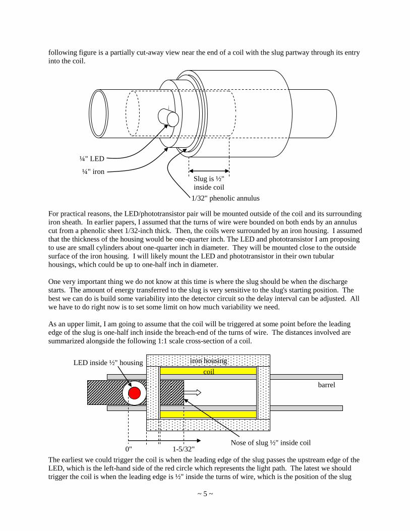
following figure is a partially cut-away view near the end of a coil with the slug partway through its entry
into the coil.
For practical reasons, the LED/phototransistor pair will be mounted outside of the coil and its surrounding
iron sheath. In earlier papers, I assumed that the turns of wire were bounded on both ends by an annulus
cut from a phenolic sheet 1/32-inch thick. Then, the coils were surrounded by an iron housing. I assumed
that the thickness of the housing would be one-quarter inch. The LED and phototransistor I am proposing
to use are small cylinders about one-quarter inch in diameter. They will be mounted close to the outside
surface of the iron housing. I will likely mount the LED and phototransistor in their own tubular
housings, which could be up to one-half inch in diameter.
One very important thing we do not know at this time is where the slug should be when the discharge
starts. The amount of energy transferred to the slug is very sensitive to the slug's starting position. The
best we can do is build some variability into the detector circuit so the delay interval can be adjusted. All
we have to do right now is to set some limit on how much variability we need.
As an upper limit, I am going to assume that the coil will be triggered at some point before the leading
edge of the slug is one-half inch inside the breach-end of the turns of wire. The distances involved are
summarized alongside the following 1:1 scale cross-section of a coil.
The earliest we could trigger the coil is when the leading edge of the slug passes the upstream edge of the
LED, which is the left-hand side of the red circle which represents the light path. The latest we should
trigger the coil is when the leading edge is ½" inside the turns of wire, which is the position of the slug
Slug is ½"
inside coil
1/32" phenolic annulus
¼" LED
¼" iron

~ 6 ~
shown in the figure. By adding up the various thicknesses, one can see that the slug could travel
anywhere between zero and 1.156 inches, or 29.5 millimeters, from the breach-side of the LED before we
trigger the discharge. How long it takes the slug to travel through this distance depends on how fast it is
going as it approaches this coil. For design purposes, I am going to assume that the slug is travelling
between 20 meters per second and 100 meters per second. (The slug will not be at rest. It is a rest for the
first coil only, and the manual trigger circuit controls the first coil.) The lengths of time it takes the slug
to travel 29.5 millimeters at these two speeds are as follows:
It is the maximum interval, about 1.5 milliseconds, which constitutes the upper limit of the timing delay.
If the timer can handle the maximum interval, it will be able to handle the minimum interval, too. The
following diagram shows what we want the circuit to do.
Aside: It is not possible to design a circuit which will respond instantaneously to the blockage of a light
path. Phototransistors are slow. The one I describe below has rise and fall times of six
microseconds (6μs) even when the light source is turned on or off extremely quickly. When the
slug passes through the light path, the change from light to dark will take even longer. At a speed
of 20 meters per second, for example, it will take the slug just to
pass from one edge of the LED to the other edge, one-quarter of an inch away.
We are more interested in repeatability than in instantaneousity(?). The potentiometers in the
circuit can be varied to give the best results. Once they have been set as desired, all we need is
for the circuit to behave in the same way, and to give the same delay interval, at every firing.
The LED and phototransistor I plan to use are manufactured by Optek. They are intended to be used with
each other. Their peak sensitivity is at a wavelength of 890 nanometers, corresponding to a frequency of
. This is getting near the high end of infrared (heat)
frequencies. These two components can be used in applications where they are mounted up to an inch or
two apart, from lens to lens. When they face each other through our brass barrel, they will be about five-
eights of an inch apart. They are going to be wired into the following circuits.
time
Output voltage
12V pulse 10μs long
Variable interval 0 to 1500μs
time
LED illumination
Light Slug's nose
blocks light path
Dark
Light

~ 7 ~
The infrared LED (D1) on one side of the barrel is wired in series with 68Ω resistor R1. The datasheet
for the OP290A diode states that its sustainable collector current is 150mA. We want the light to shine as
brightly as possible, without exceeding its current limit, so I have biased it for collector current of
125mA. From one of the charts included in the datasheet, one can see that the forward voltage drop at
this current will be about 1.5 Volts. That leaves a voltage drop of 12 – 1.5 = 10.5 Volts over resistor R1.
We can use Ohm's Law to calculate the appropriate resistance. If resistor R1 has a voltage drop of 10.5V
when current of 125mA flows through, then its resistance is R = V I = 10.5 0.125 = 84Ω. The nearest
standard resistance value is 82Ω. The power which resistor R1 must dissipate if the LED is continuously
illuminated will be P = I2R = 0.125
282 = 1.3 Watts.
Phototransistor D2 is on the other side of the barrel. Internally, the OP599A is like any other npn
transistor. Externally, though, it does not have the usual three terminals: collector, emitter and base. That
is because the function of the base, which controls the current flowing through the main collector-to-
emitter pathway, is provided by the photovoltaic effect. The incident light knocks electrons off the atoms
in the base material. Those free electrons constitute what would be called the "base current" in a usual
transistor setup.
The value of resistor R2 is chosen to maximize the "difference" between the conditions which exist when
no light falls of D2 and the conditions when D2 is fully illuminated. The variable we want to be most
different is the voltage at the anode of D2, which is the bottom terminal of D2 as it is oriented in the
schematic.
When no light falls on D2, its internal npn transistor will be cut off. No current will flow through the
main pathway. Since no current flows through, the base of transistor Q1 is in effect grounded through the
series pair of R2 and R3. This means that the voltage drop over diode D2 is the full 12V supply voltage.
Incidentally, note that this reverse biases the diode.
Now, let's look at D2 when its light-sensitive base is fully-illuminated. The base current will be relatively
high and, as transistors do, the current flowing through the main channel will be amplified. The value of
resistor R2 is high enough that D2 will be driven into its saturation mode. It will pass as much current as
the external components demand (at least up to the point where D2 burns itself up). The datasheet states
that, when D2 is saturated, the voltage between its terminals VCE(SAT) will be approximately 0.4 Volts.
This means that the voltage drop over resistor R2 will be 12 – 0.4 = 11.6 Volts. The datasheet tells us
something else as well. The minimum value of the main current IC(ON) is 2.35mA. Particular devices may
have higher main currents than this, but none will have less. If the main current through D2 is 2.35mA,
then the current flowing through resistor R2 will also be 2.35mA. (50K resistor R3 is so high that

~ 8 ~
virtually none of the current will be diverted into the base of transistor Q1.) We can use Ohm's Law once
more to find the resistance that matches a voltage drop of 11.6 Volts with a current of 2.35mA. We get:
R = V I = 11.6 0.00235 = 4,936Ω. I have not used this value for R2. Why?
Optek (the manufacturer of D1 and D2) has issued Application Bulletin #248 with some tips about using
components like these. Optek suggests that the value of the load resistance can and should be increased
for three reasons: (i) degradation over time, (ii) ambient temperatures higher than room temperature and
(iii) restatement of IC(ON) when the collector-emitter voltage is 0.4 Volts rather than 5 Volts. The second
reason is not an issue in our application, since I will use this coil gun in laboratory conditions. For
practical purposes, the first reason is not an issue either. Optek uses the word "degradation" as something
that happens after 10,000 hours of operation. I do not expect that my coil gun will be turned on for more
than a couple of hours during its entire life. But the third reason, which is rather technical, does apply to
our calculation, and I will use the discount factor 20% which Optek suggests. I have divided 4,936Ω by
80%, which gives 6,170Ω, as the value for R2. 6.2K is a nearby standard resistance value.
Transistor Q1 is a common general-purpose 2N2222A npn transistor. I have used it as a buffer between
the phototransistor and the circuitry which follows. Q1 is wired up in a typical on-off switching
configuration. When the slug's leading edge passes through the optical slot, and the light path changes
from light to dark, the voltage at D2's anode/emitter will fall from 11.6 Volts to 0 Volts. In the former
circumstance, some current will flow through base resistor R3. If Q1's base-to-emitter junction is
forward-biased, the voltage drop will be the usual silicon p-n junction voltage, about 0.7 Volts. The
voltage drop over R3 will be equal to 11.6 – 0.7 = 10.9 Volts. The current flowing through R3 will be
(Ohm's Law once again) I = V R = 10.6 50K = 0.212mA. The 2N2222A is a good current amplifier.
Its datasheet states that its dc current gain (HFE) is a minimum of 751, so the collector current will be 75
times greater than the base current, or 75 0.212mA = 15.9mA. If this much current flows into the
collector terminal, then the voltage drop over 2K resistor R4 will be V = IR = 0.0159 2000 = 31.8 Volts.
That is not possible in a circuit with a 12V supply voltage. The inconsistency is resolved by recognizing
that Q1 is not operating in is linear region, in which the collector current = HFE the base current, but has
been driven into saturation. When saturated, the voltage at Q1's emitter will be driven down to near zero.
Let me summarize the things we know so far.
Event Status / change Observation
Before anything happens Light path is continuous D2 saturated. V(D2's anode) = 11.6V
Q1 saturated. V(Q1's collector) 0V
Slug blocks light path D2 becomes cut off
Q2 becomes cut off
V(D2's anode) falls to 0V
V(Q1's collector) rises to 12V
A logic gate follows transistor Q1. It is an inverter which changes a high voltage input to a low voltage
output, and the reverse. I want to mention a characteristic of the particular inverters I am using in this
circuit. These inverters have a Schmitt-triggered input. This is very important. Most logic chips, and
particularly those CMOS devices which operate at 12 Volts, function as expected only when the voltage
transitions on their input lines are fast. Fast is, of course, a relative term. But, in our application, we are
well beyond the pale. As we have already seen, it can take the slug up to one-third of a millisecond to
eclipse the light path. The voltage transitions on D2's anode and Q1's collector will change on this rather
slow time scale.
1 The dc current gain depends on the collector current. It is 75 if the collector current is in the range of
10mA.

~ 9 ~
Schmitt-triggered inputs are designed to handle slow-moving transitions just like this. It is as if they rely
on an internally-generated voltage threshold. When the input voltage passes the threshold, the output
flips. In fact, Schmitt-triggered inputs have two internally-generated thresholds, one for low-to-high
transitions and another for high-to-low transitions. Interestingly, the former is set at a higher voltage than
the latter. Schmitt-triggered inputs are therefore able to handle some degree of noise, which could cause
the output of a normal inverter to flip back and forth. If the input voltage is heading from low to high, for
example, it has to pass a high threshold for the output to invert, and go low. But once that threshold has
been reached, the output will not change state again unless the input voltage falls quite a bit, and in
particular, falls below the other threshold voltage. This behaviour is called "hysteresis". Although noise
is not the problem in our application, the Schmitt-trigger's definite threshold voltages do solve our slow-
transition problem.
We don't really care what the exact threshold voltages are. All we need is for them to remain constant, so
that the behaviour of the circuit is repeatable from one firing to the next.
When the slug interrupts the light path, the output from inverter U2b will fall from 12V to zero. There is
a resistor-capacitor pair wired to the inverter's output. The purpose of this pair is to limit the amount of
time that the voltage stays low. Let me first explain what R5 and C1 do. Then, when I describe the
component (a timer) which follows in the circuit, I will explain why they do what they do.
I have shown voltage waveforms below the input and output lines of the R5-C1 pair. The voltage on the
input line will go from high-to-low when the slug interrupts the light path. At some later time, when the
trailing edge of the slug moves out of the optical slot, the voltage will return high.
The voltage over capacitor C1 cannot change instantaneously. When the input voltage drops from 12V
for zero, the capacitor will drag the output voltage down with it. But, C1 will start to charge up as current
flows down into it through resistor R5. The rate at which the voltage drop over C1 increases will be
determined by the time constant = R5 C1 = 1.5 103 0.01 10
-6 = 15μs. The voltage will increase at
an exponential rate, by a factor of 1 – 1/ = 0.632 of the remaining difference2 every = 10μs. We are
interested in the length of time it will take the voltage drop to rise from zero to 6V. 6 Volts is the mid-
point of the 12V supply voltage. The input line of the following component is a logic gate (or equivalent)
and will tend to change state at the halfway point, which is to say, 6 Volts. It is a fact that an exponential
waveform reaches its halfway point after an interval of time equal to a fraction of one time
constant, in our case 0.693 15μs = 10.4μs. From the point-of-view of the input gate of the following
2 is the natural number. Its value is approximately 2.718281 . The "remaining difference" is the
applied voltage (12V) less the instantaneous voltage drop over the capacitor. At the start of charging, the
instantaneous voltage is zero, the remaining difference is 12V and the change in voltage during the first
time constant (10μs) will be 0.632 12 = 7.58 Volts.
12V
0V
10.4μs

~ 10 ~
component, the driving waveform looks like a negative pulse with a duration of 10.4μs. That will be
perfectly satisfactory.
Note what happens when the slug finishes its traverse of the light path. When the trailing edge of the slug
moves out of the way, the input line of the R5-C1 pair will rise suddenly from zero to 12 Volts. The
capacitor will by this time be charged up to 12 Volts. Since the voltage drop over the capacitor cannot
change instantaneously, the voltage on the output line will shoot up to 24 Volts. C1 will start to discharge
through R5, with the discharge current flowing into the power supply. The discharge will be exponential
and the rate of decay will have the same time constant as before. These changes in voltage take place at
levels well above the switching voltage of the following component. It will not be effected by them. (Of
course, we will have to check and make sure that this kind of short voltage spike will not destroy the
component.)
The schematic at the right shows the
components which follow in the
circuit. U1 is a 555 timer, wired up
to produce a single pulse
(monostable) when it is triggered.
A negative-going pulse on pin #2,
like the one we have just created,
triggers the cycle. The output
voltage on pin #3 goes high as soon
as the timer is triggered. It remains
high for a length of time which we,
as designers, set using external
resistors and capacitors. Here, it is
resistors R6, R7 and R8, and
capacitor C2, which determine the
duration of the output pulse.
Mathematically, the duration of the output pulse – the length of time it remains high – is the
multiplicative product Tpulse = 1.1 (R6 R7 R8) C2. This is the length of time – 1.5 milliseconds
– which we figured out at the start of this section. This is the maximum delay which we want between the
triggering event and the start of the drive capacitor's discharge. I have chosen the potentiometers so that
they give this delay when they are adjusted to their maximum values. When they are adjusted to lower
resistances, the delay will be shorter.
The resistance which determines the timing is the sum of three resistors in series. 10K potentiometer R8
is the bigger of the two. It provides "coarse tuning", if you will. The delay time is "fine-tuned" using the
smaller 1K potentiometer R7. Resistor R6 is shown as having zero resistance. I have put it in the circuit
for a completely different reason. When I lay out the printed circuit board for this circuit, the existence of
R6 will ensure that there is sufficient space and copper pads for a normal resistor. In the prototype, the
gap will simply be jumpered closed. If it becomes necessary to increase the amount of delay, the jumper
can be removed and a normal discrete resistor soldered in.
As it stands, the maximum value of resistance R6 R7 R8 is 11KΩ. Accompanied by C2 = 0.12μF,
the maximum duration of the 555's output pulse will be Tpulse = 1.1 11K 0.12μ = 1.45ms. This is
close enough for our purposes.

~ 11 ~
Capacitor C4 is recommended by the manufacturer when the control voltage pin is not used. Capacitor
C5 is a small bypass capacitor used to damp down voltage spikes in the power supply which might
otherwise adversely effect the chip.
Let's turn our attention to the R9-C3 resistor capacitor pair which is attached to the timer's output pin.
The timer produces a nice pulse, but it is not a pulse we can use to trigger current flow in the coil's circuit.
We want the triggering pulse for the coil to appear when the 555's pulse ends. The 555's pulse will end
with a falling edge. We will process this falling edge in exactly the same way as we used the R5-C1 pair
to process the falling edge which came from transistor Q1. It will have the same 15μs time constant,
which will cause inverter U2c to flip state after about 10μs.
The complete schematic for this phototransistor location detector, and a list of parts, is given in Appendix
"B".
Circuit #3 - Speed measurement circuit
I am going to place a speed measurement sensor near the end of the brass tube. The sensor will consist of
two infrared LED / phototransistor pairs just like the ones I used above as location sensors to trigger the
individual coils. The longitudinal distance between the two sensors is not critical so long as it is carefully
measured. I plan on mounting them five centimeters, or about two inches apart. When the nose of the
slug passes through the optical slot of the first sensor, a timing circuit will start counting. It will stop
counting when the nose of the slug interrupts the second light path. I will use a crystal (or equivalent) to
determine the width of the pulses which get counted. A speed measurement therefore consists of simply
the number of pulses counted. If that number is and if the frequency of the crystal is , then the nose of
the slug travelled from the first sensor to the second in a period of time equal to , in seconds. If
is the distance between the two sensors (measured from a given point on one of the sensors to the
corresponding point on the other), then the speed of the slug is calculated as:
The physical layout of the speed measurement sensors is shown in the following diagram.
As with the earlier circuit, it is not essential that the sensors and the processing circuit be "fast". It is
much more important that they operate in the same way, and introduce the same delay when starting and
stopping the timer.
brass barrel
First sensor
Second sensor
2 inches

~ 12 ~
For design purposes, we need to specify both the slowest speed and the fastest speed we want to measure.
The former value, of the slowest speed, will determine the maximum time during which counting should
be carried on. The latter value, of the fastest speed, will determine how short the individual clocking
pulses need to be. In other words, the resolution of the clocking pulses determines how fast a speed can
be measured.
I want to be able to measure speeds from 20 meters per second to 100 meters per second. I intend to use a
1MHz crystal, so the individual clocking pulses will have a duration of 1 1MHz = 1μs. And, as I have
said, I plan to mount the two sensor pairs five centimeters apart. Let's look at the result of this
combination of parameters.
For the slowest speed, the count will be:
For the fastest speed, the count will be:
The conclusion to draw from the first calculation is that, if 7-segment LED digits are used to display the
total count, then the display should have four digits. It will be able to show counts from zero to 9,999.
Now, let me re-state the characteristics of the display in another way.
The lowest measureable speed, which corresponds to the highest displayable count, is:
The resolution at low speeds can be gauged by comparing the lowest speed (count = 9,999) with the
second-lowest speed (count = 9,998), namely:
The highest measureable speed (count = 1) is equal to:
One can continue in this way to calculate the speeds which correspond to the different total counts. I have
created a table with results over a useful range of speeds, and attached it as Appendix "D".
The following snippet from the schematic shows the circuit which processes the signals from the two
sensor pairs.

~ 13 ~
With the exception of the final inverters U1b and U1e, both circuits have the same front end as the
phototransistor circuit used to detect the location of the slug in preparation for triggering the second and
following coils. The same optical components are used. Transistors Q1 and Q2 are 2N2222A npn
transistors, as before. U1 is a hex inverter, as before, with Schmitt-trigger inputs. The only difference
from before is that the follow-up R-C pair has been replaced by a second inverter. The voltage
waveforms which the first and second sensors generate are shown in the following graph.
The output waveform of each sensor is high (12V) for as long as the passing slug keeps the light path
interrupted. Since this measurement is done at the end of the barrel, the speed of the slug will be the same
as it passes by both sensors (ignoring a bit of friction with the barrel which will slow the slug down), so
the length of the two pulses should be the same. We are only interested in what happens when the nose
count Nose blocks
first sensor Nose blocks
second sensor
12V
0V
Second sensor
12V
0V
First sensor
Time
Time

~ 14 ~
passes. We will start counting at the first event and stop counting at the second. We will ignore what
happens when the trailing edge of the slug clears the optical slots, and the waveforms fall. In other
words, we do not care whether or not there is any overlap between the two pulses.
(Aside: There is a design alternative to using two separate sensors, as I have done. One could use a single
sensor and time the difference between the rising edge, when the nose passes, and the falling edge, when
the trailing edge passes. The corresponding distance from which to calculate the speed of the slug would
be the slug's length. I rejected this alternative for three reasons:
1. Using two sensors means the final display, in counts, can be used for slugs of any length, without
the need for additional count-to-speed conversion tables.
2. Using two sensors means that the nose of the slugs does not have to be square. The nose can be
shaped. All that we require is that both sensors respond to the nose's passage in the same way.
As long as both sensors respond in the same way, the distance between the "events" which cause
changes later in this circuit will correspond to the distance between the sensors.
3. The components in the circuit do not necessarily take the same time to process a falling edge as
they do to process a rising edge. Using two sensors, both responding to the same kind of rising
edge, eliminates this source of uncertainty.)
The voltage outputs from the two sensors are fed into two D-type flip-flops, as follows.
U2 is a CD4013 chip which contains two independent flip-flops. Let me describe the Reset input first.
After the gun is fired the count representing the speed will be displayed on a four-digit LED. The counter
must be cleared before the next firing. The user will push a momentary pushbutton switch to clear the
counter. This will produce a positive pulse, perhaps a tenth-of-a-second or a half-second long. I have
called this the "Reset" pulse. Among other destinations, this pulse is delivered to the Reset pins of both
of these flip-flops. A high voltage on the Reset pins will cause the Q-output lines to go low, and the
complementary /Q output lines to go high. The reset will take place whether the D and Clock input

~ 15 ~
voltages are high or low. Note that the Q-output of the first sensor's flip-flop is used, while the /Q-output
of the second sensor's flip-flop is used.
Those two outputs are delivered to a 2-input NAND gate U3a, one of four such gates on chip U3.
Immediately after the Reset pulse, one of those inputs is high and the other is low, so the output voltage
on U3a's pin #3 will be high.
Let's talk about the upper flip-flop U2a, which processes the first sensor's signal. Its D-input pin (pin #5)
is tied high. When a rising edge appears on its Clock pin (pin #3), the D-voltage will be passed through
to the Q-output. That event will occur when the nose of the slug blocks the light path of the first sensor.
U2a's Q-output will rise from zero to 12V. And, it will stay there. The falling edge which will appear on
Clock pin #3 when the slug finally passes by and opens up the light path will have no impact on the
output of this flip-flop.
The lower flip-flop deals with the second sensor's signal. Its D-line (pin #9) is also tied high. When the
nose of the slug starts to block the light path of the second sensor, a rising edge will appear on the Clock
pin (pin #11) and the positive D-voltage will be passed through to the Q-output on pin #13. At the same
time, the complement (zero Volts) will appear on the /Q line (pin #12). The voltage on pin #12 will fall
from 12V to 0V. And, it, too, will stay there. The falling edge which will appear on Clock pin #11 when
the slug finally clears the second sensor will have no impact on the output of this flip-flop.
The following are the relevant waveforms.
The output of NAND gate U3a is high except in the special circumstances when both of its input lines are
high. In that case, and that case only, the output from U3a is low. NAND gate U3b inverts that negative
pulse. And, it is during the high pulse from U3b that we want to count the 1MHz clocking pulses.
12V
0V
First sensor's Q-output
Time
count Nose blocks
first sensor Nose blocks
second sensor
12V
0V
NAND gate U3a's output
Second sensor's /Q output
Time
12V
0V
Time

~ 16 ~
In the schematic above, component X1 is a 1MHz resonator. It has some built-in capacitors which make
it a little more versatile and robust than a traditional crystal but, for all intents and purposes, it acts just
like one. In the circuit, I have followed the resonator up with one of the spare NAND gates on chip U3,
just to provide a buffer and ensure that the waveform is as square as possible. The output from NAND
gate U3c will be a continuous square wave with a frequency of 1MHz. This waveform will be generated
whenever the circuit is powered up. It is not affected by the Reset pulses I described above.
The last NAND gate U3d is the one which combines the 1MHz square wave with the output from the flip-
flops. In a sense, the output of the flip-flops, which is the high pulse generated by U3b, is a "permission
window". The fast clocking pulses are permitted to pass through the window only when the flip-flops
allow. A counting pulse will occur only when both input lines of NAND gate U3d are high. This is
shown in the following figure.
The rising and falling edges of the permission window will not necessarily happen at the very same time
that the crystal's 1MHz clocking pulses are changing state. It follows that there will be uncertainty of up
to one-half pulse at the start of the window and another one-half pulse at the end. Whatever the count
turns out to be, it could be one pulse, corresponding to 1 microsecond, higher or lower than true.
The pulse train from NAND gate U3d is the input signal to a sequence of four decade counters. There is
one counter for each digit in the four-digit numeric LED display. The counter chips are CD4026BE
decade counters. They are useful in this application because their output pins are designed especially to
drive 7-segments LEDs. The following schematic shows the circuit for the second-most least-significant
digit (the 10's digit). The pulse train is applied to the Clock pin (pin #1). On overflow, when the count in
this chip rolls over from "9" to "0", a positive pulse is delivered to the Carry-out pin (pin #5), where it is
used as the clocking pulse for the counter chip of the next higher digit (the 100's digit). The Display-
inhibit pin (pin #3) and the Clock-inhibit pin (pin #2) are not used in this application, so these pin are tied
high or low as appropriate to nullify their action.
count Nose blocks
first sensor Nose blocks
second sensor
12V
0V
NAND gate U3b's output
Time
NAND gate U3c's output
Time
12V
0V
Time
12V
0V
NAND gate U3d's output

~ 17 ~
The 7-segment LED display chip driven by U5 is component U9. Like all such LED display chips, it
consists of seven individual segment LED's which are arranged in a manner so that the whole appears like
the Arabic numerals when the appropriate individual segment LED's are illuminated. Since the cathodes
of the individual segment LED's are tied together, this is a "common cathode" type of LED chip. As I
have said, the CD4026BE counter is organized so that it has one output line for each individual segment
LED. There is a resistor in series with each segment LED to control the amount of current which is
allowed to flow through. For convenience, I have used a resistor array, R10. The array is a 16-pin DIP
chip, with eight independent resistors inside. Only seven of the eight resistors in each array are used.
Like all CMOS chips, the counter chip (U5) has a limited
ability to deliver output current. The datasheet states that the
current which each output pin can supply when in the high
voltage state (12 Volts) is typically about 6.8mA (at room
temperature), but it can be as low as 3.4mA.
The 7-segment LED display chips I have chosen to use (U9 is
one of four) are DigiKey's part #516-1229-5-ND. These ones
happen to be made by Avago, and are Avago's part #HDSP-
H103. I am going to use the resistors R10 to bias the
segments to a current of 4mA at a forward voltage of 1.7
Volts. These happen to be relatively big, with easy-to-read
digits (14.2 millimeters, or more than one-half inch, high) but,
more importantly, they can operate on the current which U5 is
able to supply.
In order for the voltage drop over the LED's to be 1.7 Volts, the voltage drop over the resistors must be
12 – 1.7 = 10.3V. In order to limit the current flowing through the resistors and the LED's to 4mA, the
value of the resistance must be R = V I = 10.3 0.004 = 2,575Ω. The nearest standard 8-resistor array is
2.7K. I used Digikey part #4116R-1-272LF-ND.
The manual pushbutton used to reset the speed measurement display is shown in this schematic, too. It is
a straightforward momentary-on SPST switch, which provides a positive voltage (12V) as long as the
user keeps it pressed. When this positive voltage is applied to the Reset pin (pin #15) of U5, the
internally stored count is reset to zero. It is this same Reset pulse which is used to reset the two flip-flops
described above. Neither of these reset functions is time-critical, so I have not bothered to debounce this
switch
The complete schematic for the speed measurement circuit, and a list of parts, is given in Appendix "C".
Jim Hawley
© January 2015
If you found this description helpful, please let me know. If you spot any errors or omissions, please send
an e-mail. Thank you.
~ 18 ~
Appendix "A

~ 19 ~
Appendix "B"

~ 20 ~
Appendix "C"

~ 21 ~