octal ultrasound afe with jesd204b data sheet … · octal ultrasound afe with jesd204b data sheet...
TRANSCRIPT

Octal Ultrasound AFE with JESD204BData Sheet AD9675
Rev. A Document Feedback Information furnished by Analog Devices is believed to be accurate and reliable. However, no responsibility is assumed by Analog Devices for its use, nor for any infringements of patents or other rights of third parties that may result from its use. Specifications subject to change without notice. No license is granted by implication or otherwise under any patent or patent rights of Analog Devices. Trademarks and registered trademarks are the property of their respective owners.
One Technology Way, P.O. Box 9106, Norwood, MA 02062-9106, U.S.A.Tel: 781.329.4700 ©2013–2016 Analog Devices, Inc. All rights reserved. Technical Support www.analog.com
FEATURES 8 channels of LNA, VGA, AAF, ADC, and digital RF decimator
Low power 150 mW per channel, TGC mode, 40 MSPS 62.5 mW per channel, CW mode
10 mm × 10 mm, 144-ball CSP_BGA TGC channel input referred noise: 0.82 nV/√Hz,
maximum gain Flexible power-down modes Fast recovery from low power standby mode: 2 μs
Low noise preamplifier (LNA) Input referred noise: 0.78 nV/√Hz, gain = 21.6 dB Programmable gain: 15.6 dB, 17.9 dB, or 21.6 dB 0.1 dB compression: 1000 mV p-p, 750 mV p-p, or 450 mV p-p Flexible active input impedance matching
Variable gain amplifier (VGA) Attenuator range: 45 dB, linear in dB gain control Postamp gain (PGA): 21 dB, 24 dB, 27 dB, or 30 dB
Antialiasing filter (AAF) Programmable second-order low-pass filter (LPF) from
8 MHz to 18 MHz or 13.5 MHz to 30 MHz and high-pass filter (HPF)
Analog-to-digital converter (ADC) SNR: 75 dB, 14 bits up to 125 MSPS
JESD204B Subclass 0 coded serial digital outputs CW Doppler mode harmonic rejection I/Q demodulator
Individual programmable phase rotation Dynamic range per channel: 160 dBFS/√Hz Close-in SNR: 156 dBc/√Hz, 1 kHz offset, −3 dBFS input
RF digital decimation by 2 and high-pass filter
APPLICATIONS Medical imaging/ultrasound Nondestructive testing (NDT)
GENERAL DESCRIPTION The AD9675 is designed for low cost, low power, small size, and ease of use for medical ultrasound. It contains eight channels of a variable gain amplifier (VGA) with a low noise preamplifier (LNA), a continuous wave (CW) harmonic rejection I/Q demodulator with programmable phase rotation, an antialiasing filter (AAF), an analog-to-digital converter (ADC), and a digital high-pass filter and RF decimation by 2 for data processing and bandwidth reduction.
Each channel features a maximum gain of up to 52 dB, a fully differential signal path, and an active input preamplifier termina-tion. The channel is optimized for high dynamic performance and low power in applications where a small package size is critical.
The LNA has a single-ended to differential gain that is selectable through the serial port interface (SPI). Assuming a 15 MHz noise bandwidth (NBW) and a 21.6 dB LNA gain, the LNA input SNR is 94 dB. In CW Doppler mode, each LNA output drives an I/Q demodulator that has independently programmable phase rotation with 16 phase settings.
Power-down of individual channels is supported to increase battery life for portable applications. Standby mode allows quick power-up for power cycling. In CW Doppler operation, the VGA, AAF, and ADC are powered down. The ADC contains features to maximize flexibility and minimize system cost, such as a programmable clock, data alignment, and programmable digital test pattern generation. The digital test patterns include built-in fixed patterns, built-in pseudorandom patterns, and custom user-defined test patterns entered via the SPI.

AD9675 Data Sheet
Rev. A | Page 2 of 60
TABLE OF CONTENTS Features .............................................................................................. 1
Applications ....................................................................................... 1
General Description ......................................................................... 1
Revision History ............................................................................... 2
Functional Block Diagram .............................................................. 3
Specifications ..................................................................................... 4
AC Specifications .......................................................................... 4
Digital Specifications ................................................................... 7
Switching Specifications .............................................................. 9
Absolute Maximum Ratings .......................................................... 12
Thermal Impedance ................................................................... 12
ESD Caution ................................................................................ 12
Pin Configuration and Function Descriptions ........................... 13
Typical Performance Characteristics ........................................... 16
TGC Mode ................................................................................... 16
CW Doppler Mode ..................................................................... 20
Theory of Operation ...................................................................... 21
TGC Operation ........................................................................... 21
Digital Outputs and Timing ..................................................... 29
Analog Test Tone Generation ................................................... 38
CW Doppler Operation ............................................................. 39
Digital RF Decimator ..................................................................... 40
Vector Profile .............................................................................. 40
RF Decimator .............................................................................. 41
Digital Test Waveforms .............................................................. 41
Digital Block Power Saving Scheme ........................................ 42
Serial Port Interface (SPI) .............................................................. 43
Hardware Interface ..................................................................... 43
Memory Map .................................................................................. 45
Reading the Memory Map Table .............................................. 45
Recommended Start-Up Sequence .......................................... 45
Memory Map Register Table ..................................................... 47
Memory Map Register Descriptions ........................................ 59
Outline Dimensions ....................................................................... 60
Ordering Guide .......................................................................... 60
REVISION HISTORY 1/16—Revision A: Initial Version

Data Sheet AD9675
Rev. A | Page 3 of 60
FUNCTIONAL BLOCK DIAGRAM
Figure 1.
AAFVGALNA
CWD I/QDEMODULATOR
8 CHANNELS
SERIALPORT
INTERFACE
DATARATE
MULTIPLIERREFERENCE
LOGENERATION
LO-A TO LO-H
LOSW-A TO LOSW-H
LI-A TO LI-H
LG-A TO LG-H
DVDD DRVDD
CL
K–
CL
K+
SD
IO
SC
LK
CS
B
AD
DR
0 T
OA
DD
R4
GP
O0
TO
GP
O3
RB
IAS
VR
EF
TX
_TR
IG+
TX
_TR
IG–
CWQ+
CWQ–
CWI+
CWI–
GA
IN–
GA
IN+
ML
O–
ML
O+
RE
SE
T+
RE
SE
T–
STBYPDWNAVDD2AVDD1
SERIALIZER
CMLRF DECIMATOR14-BITADC
AD9675
SERDOUT1+ TO SERDOUT4+
SERDOUT1– TO SERDOUT4–
SYSREF+SYSREF–SYNCINB+SYNCINB–
1138
1-00
1

AD9675 Data Sheet
Rev. A | Page 4 of 60
SPECIFICATIONS AC SPECIFICATIONS AVDD1 = 1.8 V, AVDD2 = 3.0 V, DVDD = 1.4 V, DRVDD = 1.8 V, 1.0 V internal ADC reference, full temperature range (0°C to 85°C), fIN = 5 MHz, low bandwidth mode, RS = 50 Ω, RFB = ∞ (unterminated), LNA gain = 21.6 dB, LNA bias = mid-high, PGA gain = 27 dB, analog gain control, VGAIN (V) = (GAIN+) − (GAIN−) = 1.6 V, AAF LPF cutoff = fSAMPLE/3 (Mode I/Mode II) = fSAMPLE/4.5 (Mode III/Mode IV), HPF cutoff = LPF cutoff/12.00, Mode I = fSAMPLE = 40 MSPS, Mode II = fSAMPLE = 65 MSPS, Mode III = fSAMPLE = 80 MSPS, Mode IV = 125 MSPS, RF decimator bypassed (Mode I/Mode II), RF decimator enabled (Mode III/Mode IV), digital high-pass filter bypassed, JESD204B link parameters: M = 8 and L = 2, unless otherwise noted. All gain setting options are listed, which can be configured via SPI registers, and all power supply currents and power dissipations are listed for the four mode settings (Mode I, Mode II, Mode III, and Mode IV).
Table 1. Parameter1 Test Conditions/Comments Min Typ Max Unit LNA CHARACTERISTICS
Gain Single-ended input to differential output 15.6/17.9/21.6 dB Single-ended input to single-ended output 9.6/11.9/15.6 dB
0.1 dB Input Compression Point LNA gain = 15.6 dB 1000 mV p-p LNA gain = 17.9 dB 750 mV p-p LNA gain = 21.6 dB 450 mV p-p 1 dB Input Compression Point LNA gain = 15.6 dB 1200 mV p-p LNA gain = 17.9 dB 900 mV p-p LNA gain = 21.6 dB 600 mV p-p Input Common Mode (LI-x, LG-x) 2.2 V Output Common Mode (LO-x) Switch off High-Z Ω Switch on 1.5 V Output Common Mode (LOSW-x) Switch off High-Z Ω Switch on 1.5 V Input Resistance (LI-x) RFB = 300 Ω, LNA gain = 21.6 dB 50 Ω
RFB = 1350 Ω, LNA gain = 21.6 dB 200 Ω 6 kΩ
Input Capacitance (LI-x) 22 pF Input Referred Noise Voltage RS = 0 Ω LNA gain = 15.6 dB 0.83 nV/√Hz LNA gain = 17.9 dB 0.82 nV/√Hz
LNA gain = 21.6 dB 0.78 nV/√Hz Input Signal-to-Noise Ratio Noise bandwidth = 15 MHz 94 dB Input Noise Current 2.6 pA/√Hz
FULL CHANNEL CHARACTERISTICS Time gain control (TGC) AAF Low-Pass Cutoff −3 dB, programmable, low bandwidth mode 8 18 MHz
−3 dB, programmable, high bandwidth mode 13.5 30 MHz In Range AAF Bandwidth
Tolerance ±10 %
Group Delay Variation f = 1 MHz to 18 MHz, VGAIN = −1.6 V to +1.6 V ±350 ps Input Referred Noise Voltage LNA gain = 15.6 dB 0.96 nV/√Hz LNA gain = 17.9 dB 0.90 nV/√Hz LNA gain = 21.6 dB 0.82 nV/√Hz Noise Figure
Active Termination Matched LNA gain = 15.6 dB, RFB = 150 Ω 5.6 dB LNA gain = 17.9 dB, RFB = 200 Ω 4.8 dB LNA gain = 21.6 dB, RFB = 300 Ω 3.8 dB Unterminated LNA gain = 15.6 dB, RFB = ∞ 3.2 dB
LNA gain = 17.9 dB, RFB = ∞ 2.9 dB LNA gain = 21.6 dB, RFB = ∞ 2.6 dB

Data Sheet AD9675
Rev. A | Page 5 of 60
Parameter1 Test Conditions/Comments Min Typ Max Unit Correlated Noise Ratio No signal, correlated/uncorrelated −30 dB Output Offset −125 +125 LSB Signal-to-Noise Ratio (SNR) fIN = 5 MHz at −12 dBFS, VGAIN = −1.6 V 69 dBFS
fIN = 5 MHz at −1 dBFS, VGAIN = 1.6 V 59 dBFS Close-In SNR fIN = 3.5 MHz at −0.5 dBFS, VGAIN = 0 V,
1 kHz offset −130 dBc/√Hz
Second Harmonic fIN = 5 MHz at −12 dBFS, VGAIN = −1.6 V −70 dBc fIN = 5 MHz at −1 dBFS, VGAIN = 1.6 V −62 dBc Third Harmonic fIN = 5 MHz at −12 dBFS, VGAIN = −1.6 V −61 dBc fIN = 5 MHz at −1 dBFS, VGAIN = 1.6 V −55 dBc Two-Tone Intermodulation
Distortion (IMD3) fRF1 = 5.015 MHz, fRF2 = 5.020 MHz, ARF1 = −1 dBFS, ARF2 = −21 dBFS, VGAIN = 1.6 V, IMD3 relative to ARF2
−54 dBc
Channel-to-Channel Crosstalk fIN1 = 5.0 MHz at −1 dBFS −60 dB Overrange condition2 −55 dB
GAIN ACCURACY TA = 25°C Gain Law Conformance Error −1.6 < VGAIN < −1.28 V 0.4 dB −1.28 V < VGAIN < +1.28 V −1.3 +1.3 dB 1.28 V < VGAIN < 1.6 V −0.5 dB VGAIN = 0 V, normalized for ideal AAF loss −0.9 +0.9 dB Channel-to-Channel Matching −1.28 V < VGAIN < +1.28 V, 1 σ 0.1 dB PGA Gain 21/24/27/30 dB
GAIN CONTROL INTERFACE Control Range Differential −1.6 +1.6 V Control Common Mode GAIN+, GAIN− 0.7 0.8 0.9 V Input Impedance GAIN+, GAIN− 10 MΩ Gain Range 45 dB Gain Sensitivity Analog 14 dB/V Digital step size 3.5 dB Response Time Analog 45 dB change 750 ns
CW DOPPLER MODE LO Frequency fLO = fMLO/M 1 10 MHz Phase Resolution Per channel, 4LO mode 45 Degrees Per channel, 8LO mode, 16LO mode 22.5 Degrees Output DC Bias (Single-Ended) CWI+, CWI−, CWQ+, CWQ− AVDD2 ÷ 2 V Output AC Current Range Per CWI+, CWI−, CWQ+, CWQ−, each channel
enabled (2 fLO and baseband signal) ±2.2 ±2.5 mA
Transconductance (Differential) Demodulated IOUT/VIN, per CWI+, CWI−, CWQ+, CWQ−
LNA gain = 15.6 dB 3.3 mA/V LNA gain = 17.9 dB 4.3 mA/V LNA gain = 21.6 dB 6.6 mA/V Input Referred Noise Voltage RS = 0 Ω, RFB = ∞ LNA gain = 15.6 dB 1.6 nV/√Hz LNA gain = 17.9 dB 1.3 nV/√Hz LNA gain = 21.6 dB 1.0 nV/√Hz Noise Figure RS = 50 Ω, RFB = ∞ LNA gain = 15.6 dB 5.7 dB LNA gain = 17.9 dB 4.5 dB LNA gain = 21.6 dB 3.4 dB Input Referred Dynamic Range RS = 0 Ω, RFB = ∞ LNA gain = 15.6 dB 164 dBFS/√Hz LNA gain = 17.9 dB 162 dBFS/√Hz LNA gain = 21.6 dB 160 dBFS/√Hz

AD9675 Data Sheet
Rev. A | Page 6 of 60
Parameter1 Test Conditions/Comments Min Typ Max Unit Close-In SNR −3 dBFS input, fRF = 2.5 MHz, fLO = 40 MHz,
1 kHz offset, 16LO mode, one channel enabled 156 dBc/√Hz
−3 dBFS input, fRF = 2.5 MHz, fLO = 40 MHz, 1 kHz offset, 16LO mode, eight channels enabled
161 dBc/√Hz
Two-Tone Intermodulation Distortion (IMD3)
fRF1 = 5.015 MHz, fRF2 = 5.020 MHz, fLO = 80 MHz, ARF1 = −1 dBFS, ARF2 = −21 dBFS, IMD3 relative to ARF2
−58 dBc
LO Harmonic Rejection −20 dBc Quadrature Phase Error I to Q, all phases, 1 σ 0.15 Degrees I/Q Amplitude Imbalance I to Q, all phases, 1 σ 0.015 dB Channel to Channel Matching Phase I to I, Q to Q, 1 σ 0.5 Degrees Amplitude I to I, Q to Q, 1 σ 0.25 dB
POWER SUPPLY Mode I/Mode II/Mode III/Mode IV AVDD1 1.7 1.8 1.9 V AVDD2 2.85 3.0 3.6 V DVDD 1.3 1.4 1.9 V DRVDD 1.7 1.8 1.9 V IAVDD1 TGC mode, low bandwidth mode 148/187/
223/291 mA
CW Doppler mode 4 mA IAVDD2 TGC mode, no signal, low bandwidth mode 230 mA TGC mode, no signal, high bandwidth mode 239 mA CW Doppler mode 140 mA IDVDD 29/46/40/61 mA DVDD = 1.8 V 38/60/54/80 mA IDRVDD Four-lane mode, JESD204B lane rates =
1.6 Gbps/2.6 Gbps/1.6 Gbps/2.5 Gbps 121/168/
122/166 mA
Two-lane mode, JESD204B lane rates = 3.2 Gbps/5.0 Gbps/3.2 Gbps/5.0 Gbps
127/186/ 129/184
mA
One-lane mode, RF decimator enabled, JESD204B lane rates = 3.2 Gbps/5.0 Gbps/ not valid/not valid
73/105/not valid/not valid
mA
Total Power Dissipation (Including Output Drivers)
TGC mode, no signal, two-lane mode 1200/1415/ 1365/1615
1445/1680/1635/1910
mW
TGC mode, no signal, two-lane mode, DVDD = 1.8 V
1230/1460/ 1410/1675
mW
CW Doppler mode, eight channels enabled 500 mW Power-Down Dissipation 5 30 mW Standby Power Dissipation 725 mW
ADC Resolution 14 Bits SNR 75 dB
ADC REFERENCE Output Voltage Error VREF = 1 V ±50 mV Load Regulation at 1.0 mA VREF = 1 V 2 mV Input Resistance 7.5 kΩ
1 See the AN-835 Application Note, Understanding High Speed ADC Testing and Evaluation, for a complete set of definitions and information about how these tests were completed. 2 The overrange condition is specified as 6 dB more than the full-scale input range.

Data Sheet AD9675
Rev. A | Page 7 of 60
DIGITAL SPECIFICATIONS AVDD1 = 1.8 V, AVDD2 = 3.0 V, DVDD = 1.4 V, DRVDD = 1.8 V, 1.0 V internal ADC reference, full temperature range (0°C to 85°C), unless otherwise noted.
Table 2. Parameter1 Temperature Min Typ Max Unit INPUTS (CLK+, CLK−, TX_TRIG+, TX_TRIG−)
Logic Compliance CMOS/LVDS/LVPECL Differential Input Voltage2 0.2 3.6 V p-p Input Voltage Range GND – 0.2 AVDD1 + 0.2 V Input Common-Mode Voltage 0.9 V Input Resistance (Differential) 25°C 15 kΩ Input Capacitance 25°C 4 pF
INPUTS (MLO+, MLO−, RESET+, RESET−) Logic Compliance LVDS/LVPECL Differential Input Voltage2 0.250 AVDD2 × 2 V p-p Input Voltage Range GND – 0.2 AVDD2 + 0.2 V Input Common-Mode Voltage AVDD2/2 V Input Resistance (Single-Ended) 25°C 20 kΩ Input Capacitance 25°C 1.5 pF
LOGIC INPUTS (PDWN, STBY, SCLK, SDIO, ADDRx) Logic 1 Voltage Full 1.2 DRVDD + 0.3 V Logic 0 Voltage Full 0.3 V Input Resistance 25°C 30 (26 for SDIO) kΩ Input Capacitance 25°C 2 (5 for SDIO) pF
LOGIC INPUT (CSB) Logic 1 Voltage Full 1.2 DRVDD + 0.3 V Logic 0 Voltage Full 0.3 V Input Resistance 25°C 26 kΩ Input Capacitance 25°C 2 pF
LOGIC OUTPUT (SDIO)3 Logic 1 Voltage (IOH = 800 μA) Full 1.79 V Logic 0 Voltage (IOL = 50 μA) Full 0.05 V
DIGITAL OUTPUTS (SERDOUTx+, SERDOUTx−) Logic Compliance CML Differential Output Voltage (VOD) Full 400 600 750 mV Output Offset Voltage (VOS) Full 0.75 1.05 V
LOGIC OUTPUT (GPO0, GPO1, GPO2, GPO3) Logic 0 Voltage (IOL = 50 μA) Full 0.05 V
DIGITAL INPUT (SYNCINB+, SYNCINB−) Logic Compliance CMOS/LVDS Internal Bias Full 0.9 V Differential Input Voltage Range Full 0.3 3.6 V Input Voltage Range Full GND DRVDD V Input Common-Mode Range Full 0.9 1.4 V High Level Input Current Full −5 +5 μA Low Level Input Current Full −5 +5 μA Input Capacitance Full 1 pF Input Resistance Full 12 16 20 kΩ

AD9675 Data Sheet
Rev. A | Page 8 of 60
Parameter1 Temperature Min Typ Max Unit DIGITAL INPUT (SYSREF+, SYSREF−)
Logic Compliance LVDS Internal Common-Mode Bias Full 0.9 V Differential Input Voltage Full 0.3 3.6 V p-p Input Voltage Range Full GND DRVDD V Input Common-Mode Range Full 0.9 1.4 V High Level Input Current Full −5 +5 μA Low Level Input Current Full −5 +5 μA Input Capacitance Full 4 pF Input Resistance Full 8 10 12 kΩ
1 See the AN-835 Application Note, Understanding High Speed ADC Testing and Evaluation, for a complete set of definitions and information about how these tests were
completed. 2 Specified for LVDS and LVPECL only. 3 Specified for 13 SDIO pins sharing the same connection.

Data Sheet AD9675
Rev. A | Page 9 of 60
SWITCHING SPECIFICATIONS AVDD1 = 1.8 V, AVDD2 = 3.0 V, DVDD = 1.4 V, DRVDD = 1.8 V, 1.0 V internal ADC reference, L = 2, M = 8, fSAMPLE = 40 MHz, lane data rate = 3.2 Gbps, full temperature range (0°C to 85°C), unless otherwise noted.
Table 3. Parameter1 Temperature Min Typ Max Unit CLOCK2
Clock Rate (fSAMPLE) 40 MSPS (Mode I) Full 20.5 40 MHz 65 MSPS (Mode II) Full 20.5 65 MHz 80 MSPS (Mode III)3 Full 20.5 80 MHz 125 MSPS (Mode IV)4 Full 20.5 125 MHz
Clock Pulse Width High (tEH) Full 3.75 ns Clock Pulse Width Low (tEL) Full 3.75 ns
CLOCK INPUT PARAMETERS TX_TRIG± to CLK± Setup Time (tSETUP) 25°C 1 ns TX_TRIG± to CLK± Hold Time (tHOLD) 25°C 1 ns
DATA OUTPUT PARAMETERS Data Output Period or Unit Interval (UI) Full L/(20 × M × fSAMPLE) Seconds Data Output Duty Cycle 25°C 50 % Data Valid Time 25°C 0.76 UI PLL Lock Time5 25°C 26 μs Wake-Up Time (Standby) 25°C 2 μs Wake-Up Time (Power-Down)6
Device 25°C 375 μs JESD204B Link 25°C 250 μs
SYNCINB± Falling Edge to First K.28 Characters Full 4 Multiframes Code Group Synchronization (CGS) Phase K.28
Characters Duration Full 1 Multiframe
Delay (Latency) Full ADC Pipeline Full 16 Cycles RF Decimator Full 11 Cycles Digital High-Pass Filter Full 100 Cycles TX_TRIG± to Start Code (Mode I/Mode II/Mode III/
Mode IV)
Four-Lane Mode Full 31/42/30/36 Cycles Two-Lane Mode Full 31/33/30/30 Cycles
Data Rate per Lane 25°C 5.0 Gbps Uncorrelated Bounded High Probability (UBHP) Jitter 25°C 11 ps Random Jitter at 2.5 Gbps Data Rate 25°C 80 ps rms Random Jitter at 5 Gbps Data Rate 25°C 46 ps rms Output Rise/Fall Time 25°C 64 ps
TERMINATION CHARACTERISTICS Differential Termination Resistance Full 100 Ω
APERTURE Aperture Uncertainty (Jitter) 25°C <1 ps rms

AD9675 Data Sheet
Rev. A | Page 10 of 60
Parameter1 Temperature Min Typ Max Unit LO GENERATION
MLO± Frequency 4LO Mode Full 4 40 MHz 8LO Mode Full 8 80 MHz 16LO Mode Full 16 160 MHz
RESET± to MLO± Setup Time (tSETUP) Full 1 tMLO/2 ns RESET± to MLO± Hold Time (tHOLD) Full 1 tMLO/2 ns
1 See the AN-835 Application Note, Understanding High Speed ADC Testing and Evaluation, for a complete set of definitions and information about how these tests were completed. 2 Can be adjusted via the SPI. 3 Mode III must have the RF decimator enabled. 4 Mode IV must have the RF decimator enabled. 5 PLL lock time from 0 Hz to 40 MHz frequency change. 6 Wake-up time is defined as the time required to return to normal operation from power-down mode.
CLK±, TX_TRIG± Synchronization Timing Diagram
Figure 2. TX_TRIG± to CLK± Input Timing
CW Timing Diagram
Figure 3. CW Doppler Mode Input MLO±, Continuous Synchronous RESET± Timing, Sampled on the Falling MLO± Edge, 4LO Mode
Figure 4. CW Doppler Mode Input MLO±, Continuous Synchronous RESET± Timing, Sampled on the Falling MLO± Edge, 8LO Mode
CLK–
CLK+
TX_TRIG+
TX_TRIG–
tEH tEL
tSETUP
tHOLD
1138
1-00
2
MLO–
MLO+
RESET–
RESET+
tMLO
tSETUP
tHOLD
1138
1-00
4
MLO–
MLO+
RESET–
RESET+
tMLO
tHOLDtSETUP
1138
1-00
5

Data Sheet AD9675
Rev. A | Page 11 of 60
Figure 5. CW Doppler Mode Input MLO±, Pulse Synchronous RESET± Timing, 4LO/8LO/16LO Mode
Figure 6. CW Doppler Mode Input MLO±, Pulse Asynchronous RESET± Timing, 4LO/8LO/16LO Mode
MLO–
MLO+
RESET–
RESET+
tMLO
tSETUP
tHOLD
1138
1-10
5
MLO–
MLO+
RESET–
RESET+
tMLO
tSETUPtHOLD
1138
1-00
6
AD9675 Data Sheet
Rev. A | Page 12 of 60
ABSOLUTE MAXIMUM RATINGS Table 4. Parameter Rating AVDD1 to GND −0.3 V to +2.0 V AVDD2 to GND −0.3 V to +3.9 V DVDD to GND −0.3 V to +2.0 V DRVDD to GND −0.3 V to +2.0 V GND to GND −0.3 V to +0.3 V AVDD2 to AVDD1 −2.0 V to +3.9 V AVDD1 to DRVDD −2.0 V to +2.0 V AVDD2 to DRVDD −2.0 V to +3.9 V SERDOUTx+, SERDOUTx−, SDIO, PDWN,
STBY, SCLK, CSB, ADDRx to GND −0.3 V to DRVDD + 0.3 V
LI-x, LO-x, LOSW-x, CWI−, CWI+, CWQ−, CWQ+, GAIN+, GAIN−, RESET+, RESET−, MLO+, MLO−, GPO0, GPO1, GPO2, GPO3 to GND
−0.3 V to AVDD2 + 0.3 V
CLK+, CLK−, TX_TRIG+, TX_TRIG−, VREF to GND
−0.3 V to AVDD1 + 0.3 V
Operating Temperature Range (Ambient)
0°C to 85°C
Storage Temperature Range (Ambient)
−65°C to +150°C
Maximum Junction Temperature 150°C Lead Temperature (Soldering, 10 sec) 300°C
Stresses at or above those listed under Absolute Maximum Ratings may cause permanent damage to the product. This is a stress rating only; functional operation of the product at these or any other conditions above those indicated in the operational section of this specification is not implied. Operation beyond the maximum operating conditions for extended periods may affect product reliability.
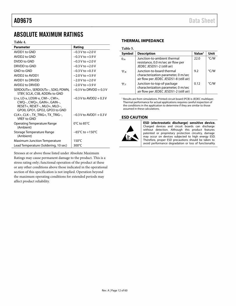
THERMAL IMPEDANCE
Table 5. Symbol Description Value1 Unit
JA Junction-to-ambient thermal resistance, 0.0 m/sec air flow per JEDEC JESD51-2 (still air)
22.0 °C/W
JB Junction-to-board thermal characterization parameter, 0 m/sec air flow per JEDEC JESD51-8 (still air)
9.2 °C/W
JT Junction-to-top-of-package characterization parameter, 0 m/sec air flow per JEDEC JESD51-2 (still air)
0.12 °C/W
1 Results are from simulations. Printed circuit board (PCB) is JEDEC multilayer.
Thermal performance for actual applications requires careful inspection of the conditions in the application to determine if they are similar to those assumed in these calculations.
ESD CAUTION

Data Sheet AD9675
Rev. A | Page 13 of 60
PIN CONFIGURATION AND FUNCTION DESCRIPTIONS
Figure 7. Pin Configuration
Figure 8. CSP_BGA Pin Location
1 2 3 4 9 10 11 125 6 7 8
A
B
C
D
E
F
G
H
J
K
L
M
LI-E LI-F LI-G LI-H LI-A LI-B LI-C LI-DVREF RBIAS GAIN+ GAIN–
LG-E LG-F LG-G LG-H LG-A LG-B LG-C LG-DGND GND CLNA GND
LO-E LO-F LO-G LO-H LO-A LO-B LO-C LO-DGND GND GND GND
LOSW-E LOSW-F LOSW-G LOSW-H LOSW-A LOSW-B LOSW-C LOSW-DGND GND GND GND
GND AVDD2 AVDD2 AVDD2 AVDD2 AVDD2 AVDD2 GNDGND GND GND GND
AVDD1 GND AVDD1 GND GND AVDD1 GND AVDD1AVDD1 GND GND AVDD1
GND AVDD1 GND DVDD AVDD1 GND DVDD GNDGND GND GND GND
CLK– TX_TRIG– GND GND ADDR2 ADDR1 ADDR0 CSBGND GND ADDR4 ADDR3
CLK+ TX_TRIG+ CWQ+ GND GPO3 GPO1 PDWN SDIOCWI+ AVDD2 MLO+ RESET–
GND GND CWQ– GND GPO2 GPO0 STBY SCLKCWI– AVDD2 MLO– RESET+
DRVDD SYNCINB+ SYSREF+ NIC NIC DRVDDSERDOUT4+ SERDOUT3+ SERDOUT2+ SERDOUT1+
GND SYNCINB– SYSREF– NIC NIC
NIC NIC
NIC NIC GNDSERDOUT4– SERDOUT3– SERDOUT2– SERDOUT1–
1138
1-00
7
NIC = NOT INTERNALLY CONNECTED.
A
B
C
D
E
F
G
J
H
K
L
M
2 6 10 124 81 3 5 7 119
TOP VIEW(Not to Scale) 11
381-
008

AD9675 Data Sheet
Rev. A | Page 14 of 60
Table 6. Pin Function Descriptions Pin No. Mnemonic Description B5, B6, B8, C5, C6, C7, C8, D5, D6, D7, D8, E1, E5, E6, E7, E8, E12, F2, F4, F6, F7, F9, F11, G1, G3, G5, G6, G7, G8, G10, G12, H3, H4, H5, H6, J4, K1, K2, K4, M1, M12
GND Ground. These pins are tied to a quiet analog ground.
F1, F3, F5, F8, F10, F12, G2, G9 AVDD1 1.8 V Analog Supply. G4, G11 DVDD 1.4 V Digital Supply. E2, E3, E4, E9, E10, E11, J6, K6 AVDD2 3.0 V Analog Supply. B7 CLNA LNA External Capacitor. L1, L12 DRVDD 1.8 V Digital Output Driver Supply. C1 LO-E LNA Analog Inverted Output for Channel E. D1 LOSW-E LNA Analog Switched Output for Channel E. A1 LI-E LNA Analog Input for Channel E. B1 LG-E LNA Ground for Channel E. C2 LO-F LNA Analog Inverted Output for Channel F. D2 LOSW-F LNA Analog Switched Output for Channel F. A2 LI-F LNA Analog Input for Channel F. B2 LG-F LNA Ground for Channel F. C3 LO-G LNA Analog Inverted Output for Channel G. D3 LOSW-G LNA Analog Switched Output for Channel G. A3 LI-G LNA Analog Input for Channel G. B3 LG-G LNA Ground for Channel G. C4 LO-H LNA Analog Inverted Output for Channel H. D4 LOSW-H LNA Analog Switched Output for Channel H. A4 LI-H LNA Analog Input for Channel H. B4 LG-H LNA Ground for Channel H. H1 CLK− Clock Input Complement. J1 CLK+ Clock Input True. H2 TX_TRIG− Transmit Trigger Complement. J2 TX_TRIG+ Transmit Trigger True. H11 ADDR0 Chip Address Bit 0. H10 ADDR1 Chip Address Bit 1. H9 ADDR2 Chip Address Bit 2. H8 ADDR3 Chip Address Bit 3. H7 ADDR4 Chip Address Bit 4. L2, M2, L3, M3, L10, M10, L11, M11 NIC Not Internally Connected. These pins are not connected internally. Allow the
NIC pins to float, or connect them to ground. Avoid routing high speed signals through these pins because noise coupling may result.
L4 SYNCINB+ Active Low JESD204B LVDS SYNC Input—True. M4 SYNCINB− Active Low JESD204B LVDS SYNC Input—Complement. M5 SERDOUT4− Serial Lane 4 CML Output Data—Complement. L5 SERDOUT4+ Serial Lane 4 CML Output Data—True. M6 SERDOUT3− Serial Lane 3 CML Output Data—Complement. L6 SERDOUT3+ Serial Lane 3 CML Output Data—True. M7 SERDOUT2− Serial Lane 2 CML Output Data—Complement. L7 SERDOUT2+ Serial Lane 2 CML Output Data—True. M8 SERDOUT1− Serial Lane 1 CML Output Data—Complement. L8 SERDOUT1+ Serial Lane 1 CML Output Data—True. M9 SYSREF− Active Low JESD204B LVDS System Reference (SYSREF) Input—Complement. L9 SYSREF+ Active Low JESD204B LVDS SYSREF Input—True. K11 STBY Standby Power-Down. J11 PDWN Full Power-Down. K12 SCLK Serial Clock. J12 SDIO Serial Data Input/Output.

Data Sheet AD9675
Rev. A | Page 15 of 60
Pin No. Mnemonic Description H12 CSB Chip Select Bar. B9 LG-A LNA Ground for Channel A. A9 LI-A LNA Analog Input for Channel A. D9 LOSW-A LNA Analog Switched Output for Channel A. C9 LO-A LNA Analog Inverted Output for Channel A. B10 LG-B LNA Ground for Channel B. A10 LI-B LNA Analog Input for Channel B. D10 LOSW-B LNA Analog Switched Output for Channel B. C10 LO-B LNA Analog Inverted Output for Channel B. B11 LG-C LNA Ground for Channel C. A11 LI-C LNA Analog Input for Channel C. D11 LOSW-C LNA Analog Switched Output for Channel C. C11 LO-C LNA Analog Inverted Output for Channel C. B12 LG-D LNA Ground for Channel D. A12 LI-D LNA Analog Input for Channel D. D12 LOSW-D LNA Analog Switched Output for Channel D. C12 LO-D LNA Analog Inverted Output for Channel D. K10 GPO0 General-Purpose Open-Drain Output 0. J10 GPO1 General-Purpose Open-Drain Output 1. K9 GPO2 General-Purpose Open-Drain Output 2. J9 GPO3 General-Purpose Open-Drain Output 3. J8 RESET− Synchronizing Input for LO Divide by M Counter Complement. K8 RESET+ Synchronizing Input for LO Divide by M Counter True. K7 MLO− CW Doppler Multiple Local Oscillator Input Complement. J7 MLO+ CW Doppler Multiple Local Oscillator Input True. A8 GAIN− Gain Control Voltage Input Complement. A7 GAIN+ Gain Control Voltage Input True. A6 RBIAS External Resistor to Set the Internal ADC Core Bias Current. A5 VREF Voltage Reference Input/Output. K5 CWI− CW Doppler I Output Complement. J5 CWI+ CW Doppler I Output True. K3 CWQ− CW Doppler Q Output Complement. J3 CWQ+ CW Doppler Q Output True.

AD9675 Data Sheet
Rev. A | Page 16 of 60
TYPICAL PERFORMANCE CHARACTERISTICS TGC MODE Mode I = fSAMPLE = 40 MSPS, fIN = 5 MHz, low bandwidth mode, RS = 50 Ω, RFB = ∞ (unterminated), LNA gain = 21.6 dB, LNA bias = midhigh, PGA gain = 27 dB, VGAIN (V) = (GAIN+) − (GAIN−) = 1.6 V, AAF LPF cutoff = fSAMPLE/3, HPF cutoff = LPF cutoff/12.00 (default), RF decimator bypassed, digital high-pass filter bypassed, unless otherwise noted.
Figure 9. Gain Error vs. VGAIN
Figure 10. Gain Error Histogram, VGAIN = −1.28 V
Figure 11. Gain Error Histogram, VGAIN = 0 V
Figure 12. Gain Error Histogram, VGAIN = 1.28 V
Figure 13. Gain Matching Histogram, VGAIN = −1.2 V
Figure 14. Gain Matching Histogram, VGAIN = 1.2 V
2.0
–2.0–1.6 1.6
GA
IN E
RR
OR
(d
B)
VGAIN (V)
–1.5
–1.0
–0.5
0
0.5
1.0
1.5
–1.2 –0.8 –0.4 0 0.4 0.8 1.2
0°C
85°C25°C
1138
1-00
9
25
20
15
10
5
0
PE
RC
EN
TA
GE
OF
UN
ITS
(%
)
GAIN ERROR (dB)
–1.0
–0.9
–0.8
–0.7
–0.6
–0.5
–0.4
–0.3
–0.2
–0.1 0
0.1
0.2
0.3
0.4
0.5
0.6
0.7
0.8
0.9
1.0
1138
1-01
0
35
30
25
20
15
10
5
0
PE
RC
EN
TA
GE
OF
UN
ITS
(%
)
GAIN ERROR (dB)
–1.0
–0.9
–0.8
–0.7
–0.6
–0.5
–0.4
–0.3
–0.2
–0.1 0
0.1
0.2
0.3
0.4
0.5
0.6
0.7
0.8
0.9
1.0
1138
1-01
1
25
20
15
10
5
0
PE
RC
EN
TA
GE
OF
UN
ITS
(%
)GAIN ERROR (dB)
–1.0
–0.9
–0.8
–0.7
–0.6
–0.5
–0.4
–0.3
–0.2
–0.1 0
0.1
0.2
0.3
0.4
0.5
0.6
0.7
0.8
0.9
1.0
1138
1-01
2
20
15
10
5
0
PE
RC
EN
TA
GE
OF
UN
ITS
(%
)
CHANNEL TO CHANNEL GAIN MATCHING (dB)
–1.0
–0.9
–0.8
–0.7
–0.6
–0.5
–0.4
–0.3
–0.2
–0.1 0
0.1
0.2
0.3
0.4
0.5
0.6
0.7
0.8
0.9
1.0
1138
1-01
3
20
15
10
5
0
PE
RC
EN
TA
GE
OF
UN
ITS
(%
)
CHANNEL TO CHANNEL GAIN MATCHING (dB)
–1.0
–0.9
–0.8
–0.7
–0.6
–0.5
–0.4
–0.3
–0.2
–0.1 0
0.1
0.2
0.3
0.4
0.5
0.6
0.7
0.8
0.9
1.0
1138
1-01
4

Data Sheet AD9675
Rev. A | Page 17 of 60
Figure 15. Short-Circuit, Input Referred Noise vs. Frequency
Figure 16. Short-Circuit, Output Referred Noise vs. Channel Gain, LNA Gain = 21.6 dB, PGA Gain = 21 dB, VGAIN = 1.6 V
Figure 17. SNR vs. Channel Gain and PGA Gain, AOUT = −1.0 dBFS
Figure 18. SNR vs. Channel Gain and LNA Gain, AOUT = −1.0 dBFS
Figure 19. SNR vs. Channel Gain and PGA Gain, AIN = −45 dBm
Figure 20. Antialiasing Filter (AAF) Pass-Band Response, LPF Cutoff = 1 × (1/3) × fSAMPLE, HPF = 1/12 × LPF Cutoff
1.4
1.2
1.0
0.8
0.6
0.41 10
INP
UT
RE
FE
RR
ED
NO
ISE
(n
V/√
Hz)
FREQUENCY (MHz)
2 3 4 5 6 7 8 9
1138
1-01
5–132
–146–5 45
OU
TP
UT
RE
FE
RR
ED
NO
ISE
(d
Bc/√H
z)
CHANNEL GAIN (dB)
–144
–142
–140
–138
–136
–134
0 5 10 15 20 25 30 35 40
PGA GAIN = 21dB11
381-
016
70
5010 55
SN
R (
dB
FS
)
CHANNEL GAIN (dB)
52
54
56
58
60
62
64
66
68
15 20 25 30 35 40 45 50
PGAGAIN = 21dB
PGAGAIN = 27dB
PGAGAIN = 30dB
PGAGAIN = 24dB
1138
1-01
7
70
5010 55
SN
R (
dB
FS
)
CHANNEL GAIN (dB)
52
54
56
58
60
62
64
66
68
15 20 25 30 35 40 45 50
LNAGAIN = 17.9dB
LNAGAIN = 21.6dB
LNAGAIN = 15.6dB
1138
1-01
8
74
54–5 55
SN
R(d
BF
S)
CHANNEL GAIN (dB)
56
58
60
62
64
66
68
70
72
151050 20 25 30 35 40 45 50
PGAGAIN = 21dB
PGAGAIN = 30dB
PGAGAIN = 27dB
PGAGAIN = 24dB
1138
1-01
9
0
–100 2015105
AM
PL
ITU
DE
(d
BF
S)
INPUT FREQUENCY (MHz)
–9
–8
–7
–6
–5
–4
–3
–2
–1
SPEED MODE = I (40MSPS)LOW BANDWIDTH MODE
1138
1-02
0

AD9675 Data Sheet
Rev. A | Page 18 of 60
Figure 21. Second-Order and Third-Order Harmonic Distortion vs. Input Frequency
Figure 22. Second-Order Harmonic Distortion vs. Channel Gain, AOUT = −1.0 dBFS
Figure 23. Third-Order Harmonic Distortion vs. Channel Gain, AOUT = −1.0 dBFS
Figure 24. Second-Order Harmonic Distortion vs. ADC Output Level (AOUT)
Figure 25. Third-Order Harmonic Distortion vs. ADC Output Level (AOUT)
Figure 26. TGC Path Phase Noise, LNA Gain = 21.6 dB, PGA Gain = 27 dB, VGAIN = 0 V
0
–1002 11
HA
RM
ON
IC D
IST
OR
TIO
N (
dB
FS
)
INPUT FREQUENCY (MHz)
–90
–80
–70
–60
–50
–40
–30
–20
–10
3 4 5 6 7 8 9 10
MIN VGAIN, AOUT = –12.0dBFSMAX VGAIN, AOUT = –1.0dBFS
THIRD-ORDER, MIN VGAIN
THIRD-ORDER, MAX VGAIN
SECOND-ORDER, MIN VGAIN
SECOND-ORDER, MAX VGAIN
1138
1-02
1
0
–10010 50
SE
CO
ND
-OR
DE
R H
AR
MO
NIC
DIS
TO
RT
ION
(d
BF
S)
CHANNEL GAIN (dB)
–90
–80
–70
–60
–50
–40
–30
–20
–10PGAGAIN = 24dB
15 20 25 30 35 40 45
LNAGAIN = 17.9dB
LNAGAIN = 15.6dB
LNAGAIN = 21.6dB
1138
1-02
2
0
–10010 45
TH
IRD
-OR
DE
R H
AR
MO
NIC
DIS
TO
RT
ION
(d
BF
S)
CHANNEL GAIN (dB)
–90
–80
–70
–60
–50
–40
–30
–20
–10PGAGAIN = 24dB
15 20 25 30 35 40
LNAGAIN = 15.6dB
LNAGAIN = 21.6dB
LNAGAIN = 17.9dB
1138
1-02
3
0
–120–40 0
SE
CO
ND
-OR
DE
R H
AR
MO
NIC
DIS
TO
RT
ION
(d
BF
S)
ADC OUTPUT LEVEL (dBFS)
–110
–100
–90
–80
–70
–60
–50
–40
–30
–20
–10
–35 –30 –25 –20 –15 –10 –5
VGAIN = 0V
VGAIN = –1.2V
VGAIN = +1.6V
1138
1-02
4
0
–120–40 0
TH
IRD
-OR
DE
R H
AR
MO
NIC
DIS
TO
RT
ION
(d
BF
S)
ADC OUTPUT LEVEL (dBFS)
–110
–100
–90
–80
–70
–60
–50
–40
–30
–20
–10
–35 –30 –25 –20 –15 –10 –5
VGAIN = –1.2V
VGAIN = +1.6V
VGAIN = 0V
1138
1-02
5
–100
–160
–150
–140
–130
–120
–110
100 100k10k1k
PH
AS
E N
OIS
E (
dB
c/√H
z)
OFFSET FREQUENCY FROM CARRIER (Hz) 1138
1-02
6
Data Sheet AD9675
Rev. A | Page 19 of 60
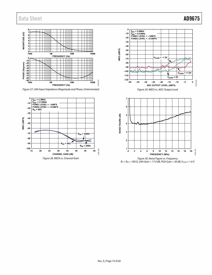
Figure 27. LNA Input Impedance Magnitude and Phase, Unterminated
Figure 28. IMD3 vs. Channel Gain
Figure 29. IMD3 vs. ADC Output Level
Figure 30. Noise Figure vs. Frequency RS = RIN = 100 Ω, LNA Gain = 17.9 dB, PGA Gain = 30 dB, VGAIN = 1.6 V
876543210
0–10–20–30–40–50–60–70–80–90
100k 1M 10M 100MFREQUENCY (Hz)
FREQUENCY (Hz)
PH
AS
E (
Deg
rees
)M
AG
NIT
UD
E (
kΩ)
100k 1M 10M 100M
1138
1-02
70
–10015 50
IMD
3 (d
BF
S)
CHANNEL GAIN (dB)
–90
–80
–70
–60
–50
–40
–30
–20
–10
20 25 30 35 40 45
fIN1 = 2.3MHzfIN2 = 2.31MHzFUND1 LEVEL = –1dBFSFUND2 LEVEL = –21dBFSRS = 50Ω
RIN = 50Ω
RIN = 1000Ω
RIN = 300Ω
1138
1-02
8
0
–120–40 0
IMD
3 (d
BF
S)
ADC OUTPUT LEVEL (dBFS)
–110
–100
–90
–80
–70
–60
–50
–40
–30
–20
–10
–35 –30 –25 –20 –15 –10 –5
VGAIN = +1.6V
VGAIN = 0V
VGAIN = –1.2V
fIN1 = 5.0MHzfIN2 = 5.01MHzFUND1 LEVEL = –1dBFSFUND2 LEVEL = –21dBFS
1138
1-02
9
7
10 20
NO
ISE
FIG
UR
E (
dB
)
FREQUENCY (MHz)
2
3
4
5
6
2 4 6 8 10 12 14 16 18
1138
1-03
1

AD9675 Data Sheet
Rev. A | Page 20 of 60
CW DOPPLER MODE fIN = 5 MHz, fLO = 20 MHz, 4LO mode, RS = 50 Ω, LNA gain = 21.6 dB, LNA bias = midhigh, all CW channels enabled, phase rotation = 0°.
Figure 31. Noise Figure vs. Baseband Frequency Figure 32. Output Referred SNR vs. Baseband Frequency
10
00 10000
NO
ISE
FIG
UR
E (
dB
)
BASEBAND FREQUENCY (Hz)
1
2
3
4
5
6
7
8
9
1000 2000 3000 4000 5000 6000 7000 8000 900011
381-
032
165
1300 10000
SN
R (
dB
c/√H
z)
BASEBAND FREQUENCY (Hz)
160
155
150
145
140
135
1000 2000 3000 4000 5000 6000 7000 8000 9000
1138
1-03
3

Data Sheet AD9675
Rev. A | Page 21 of 60
THEORY OF OPERATION
Figure 33. Simplified Block Diagram of a Single Channel
Each channel of the AD9675 contains both a TGC signal path and a CW Doppler signal path. Common to both signal paths, the LNA provides four user adjustable input impedance termination options for matching different probe impedances. The CW Doppler path includes an I/Q demodulator with programmable phase rotation needed for analog beamforming. The TGC path includes a differential X-AMP® VGA, an antialiasing filter, an ADC, and a digital RF decimation by 2 and high-pass filter. Figure 33 shows a simplified block diagram with external components.
TGC OPERATION The system gain is distributed as listed in Table 7.
Table 7. Channel Analog Gain Distribution Section Nominal Gain (dB) LNA 15.6/17.9/21.6 (LNAGAIN) Attenuator −45 to 0 (VGAATT) VGA Amplifier 21/24/27/30 (PGAGAIN) Filter 0 ADC 0
Each LNA output is dc-coupled to a VGA input. The VGA consists of an attenuator with a range of −45 dB to 0 dB followed by an amplifier with a selectable gain of 21 dB, 24 dB, 27 dB, or 30 dB. The X-AMP gain interpolation technique results in low gain error and uniform bandwidth, and differential signal paths minimize distortion.
The linear in dB gain (law conformance) range of the TGC path is 45 dB. The slope of the gain control interface is 14 dB/V, and the gain control range is −1.6 V to +1.6 V. Equation 1 is the expression for the differential voltage, VGAIN, at the gain control interface. Equation 2 is the expression for the VGA attenuation, VGAATT, as a function of VGAIN.
VGAIN (V) = (GAIN+) − (GAIN−) (1)
VGAATT (dB) = −14 (dB/V) × (1.6 − VGAIN) (2)
Then, calculate the total channel gain as in Equation 3.
Channel Gain (dB) = LNAGAIN + VGAATT + PGAGAIN (3)
In its default condition, the LNA has a gain of 21.6 dB (12×), and the VGA postamp gain is 24 dB. If the voltage on the GAIN+ pin is 0 V and the voltage on the GAIN− pin is 1.6 V (44.8 dB attenuation), the total gain of the channel is 0.8 dB if the LNA input is unmatched. The channel gain is −5.2 dB if the LNA is matched to 50 Ω (RFB = 300 Ω). However, if the voltage on the GAIN+ pin is 1.6 V and the voltage on the GAIN− pin is 0 V (0 dB attenuation), VGAATT is 0 dB. This results in a total gain of 45.6 dB through the TGC path if the LNA input is unmatched, or in a total gain of 39.6 dB if the LNA input is matched. Similarly, if the LNA input is unmatched and has a gain of 21.6 dB (12×), and the VGA postamp gain is 30 dB, the channel gain is approximately 52 dB with 0 dB VGAATT.
In addition to the analog VGA attenuation described in Equation 2, the attenuation level can be digitally controlled in 3.5 dB increments. Equation 3 is still valid, and the value of VGAATT is equal to the attenuation level set in Address 0x011, Bits[7:4].
Low Noise Amplifier (LNA)
Good system sensitivity relies on a proprietary ultralow noise LNA at the beginning of the signal chain, which minimizes the noise contribution in the following VGA. Active impedance control optimizes noise performance for applications that benefit from input impedance matching.
The LNA input, LI-x, is capacitively coupled to the source. An on-chip bias generator establishes dc input bias voltages of approximately 2.2 V and centers the output common-mode levels at 1.5 V (AVDD2 divided by 2). A capacitor, CLG, of the same value as the input coupling capacitor, CS, is connected from the LG-x pin to ground.
The LNA supports three gains, 21.6 dB, 17.9 dB, or 15.6 dB, set through the SPI. Overload protection ensures quick recovery time from large input voltages.
Low value feedback resistors and the current driving capability of the output stage allow the LNA to achieve a low input referred noise voltage of 0.78 nV/√Hz (at a gain of 21.6 dB).
POSTAMP
LNA
GAIN–
FILTERATTENUATOR–45dB TO 0dB
GAININTERPOLATOR
PIPELINEADC
LOSW-x
LO-x
LI-x
LG-x
RESET+
MLO+
MLO–
RFB2
RFB1
LOGENERATION
15.6dB,17.9dB,21.6dB
21dB,24dB,27dB,30dB
CLG
CSH
TRANSDUCER
CS
T/RSWITCH
GAIN+
SERIALCML
TX_TRIG–TX_TRIG+
RESET–
gm
CWQ+
CWQ–
CWI+
CWI–
SERDOUT1+TO SERDOUT4+
SERDOUT1–TO SERDOUT4–
SYSREF+
SYSREF–
SYNCINB+
SYNCINB–
FILTER/DEC
1138
1-03
4

AD9675 Data Sheet
Rev. A | Page 22 of 60
On-chip resistor matching results in precise single-ended gains, which are critical for accurate impedance control. The use of a fully differential topology and negative feedback minimizes distortion. Low second-order harmonic distortion is particularly important in harmonic ultrasound imaging applications.
Active Impedance Matching
The LNA consists of a single-ended voltage gain amplifier with differential outputs and the negative output externally available on two output pins (LO-x and LOSW-x) that are controlled via internal switches. This configuration allows active input impedance synthesis of 3 different impedance values (and unterminated value) via connecting up to two external resistances in parallel and controlling the internal switch states via SPI. This well known technique is used for interfacing multiple probe impedances to a single system. For example, with a fixed gain of 8× (17.9 dB), an active input termination is synthesized by connecting a feedback resistor between the negative output pin, LO-x, and the positive input pin, LI-x. The input resistance calculation is shown in Equation 4.
)21(30)20(||)20( 2
ARR
R FBFB1IN
(4)
where: RFB1 and RFB2 are the external feedback resistors. 20 Ω is the internal switch on resistance. 30 Ω is an internal series resistance common to the two internal switches. A/2 is the single-ended gain or the gain from the LI-x inputs to the LO-x outputs.
RFB can be equal to RFB1, RFB2, or (RFB1 + 20)||(RFB2 + 20) depending on the connection status of the internal switches.
Because the amplifier has a gain of 8× from its input to its differential output, it is important to note that the gain, A/2, is the gain from Pin LI-x to Pin LO-x and that it is 6 dB less than the gain of the amplifier, or 12.1 dB (4×). The input resistance is reduced by an internal bias resistor of 6 kΩ in parallel with the source resistance connected to pin LI-x, with Pin LG-x ac grounded. Use, the more accurate, Equation 5 to calculate the required RFB for a desired RIN, even for higher values of RIN.
k6||
)2/1(30)20(||)20( 2
ARR
R FBFB1IN (5)
For example, to set RIN to 200 Ω with a single-ended LNA gain of 12.1 dB (4×), the value of RFB1 from Equation 4 must be 950 Ω, while the switch for RFB2 is open. If the more accurate equation (Equation 5) is used to calculate RIN, the value is then 194 Ω instead of 200 Ω, resulting in a gain error of less than 0.27 dB. Some factors, such as the presence of a dynamic source resistance, may influence the absolute gain accuracy more significantly. At higher frequencies, the input capacitance of the LNA must be considered. The user must determine the level of matching accuracy and adjust RFB1 and RFB2 accordingly.
RFB is the resulting impedance of the RFB1 and RFB2 combination (see Figure 33). Use Register 0x02C in the SPI memory to program the AD9675 for four impedance matching options: three active terminations and unterminated. Table 8 shows an example of how to select RFB1 and RFB2 for 66 Ω, 100 Ω, and 200 Ω input impedance for LNA gain = 21.6 dB (12×).
Table 8. Active Termination Example for LNA Gain = 21.6 dB, RFB1 = 650 Ω, RFB2 = 1350 Ω Addr 0x02C Value RS (Ω)
LO-x Switch
LOSW-x Switch RFB (Ω)
RIN (Ω) (Eq. 4)
00 (default) 100 On Off RFB1 100 01 50 On On RFB1||RFB2 69 10 200 Off On RFB2 200 11 N/A1 Off Off ∞ ∞ 1 N/A means not applicable.
The bandwidth (BW) of the LNA is greater than 80 MHz. Ultimately, the BW of the LNA limits the accuracy of the synthesized RIN. For RIN = RS up to about 200 Ω, the best match is between 100 kHz and 10 MHz, where the lower frequency limit is determined by the size of the ac coupling capacitors, and the upper limit is determined by the LNA BW. Furthermore, the input capacitance and RS limit the BW at higher frequencies. Figure 34 shows RIN vs. frequency for various values of RFB.
Figure 34. RIN vs. Frequency for Various Values of RFB
(Effects of RSH and CSH Are Also Shown)
However, for larger RIN values, parasitic capacitance starts rolling off the signal BW before the LNA can produce peaking. CSH further degrades the match; therefore, do not use CSH for values of RIN that are greater than 100 Ω. Table 9 lists the recommended values for RFB and CSH in terms of RIN. CFB is needed in series with RFB because the dc levels at Pin LO-x and Pin LI-x are unequal.
10
100
1k
100k 1M 10M 100M
INP
UT
RE
SIS
TA
NC
E(Ω
)
FREQUENCY (Hz)
RS = 50Ω, RFB = 200Ω, CSH = 70pF
RS = 100Ω, RFB = 400Ω, CSH = 20pF
RS = 200Ω, RFB = 800Ω
RS = 500Ω, RFB = 2kΩ
1138
1-03
5
Data Sheet AD9675
Rev. A | Page 23 of 60
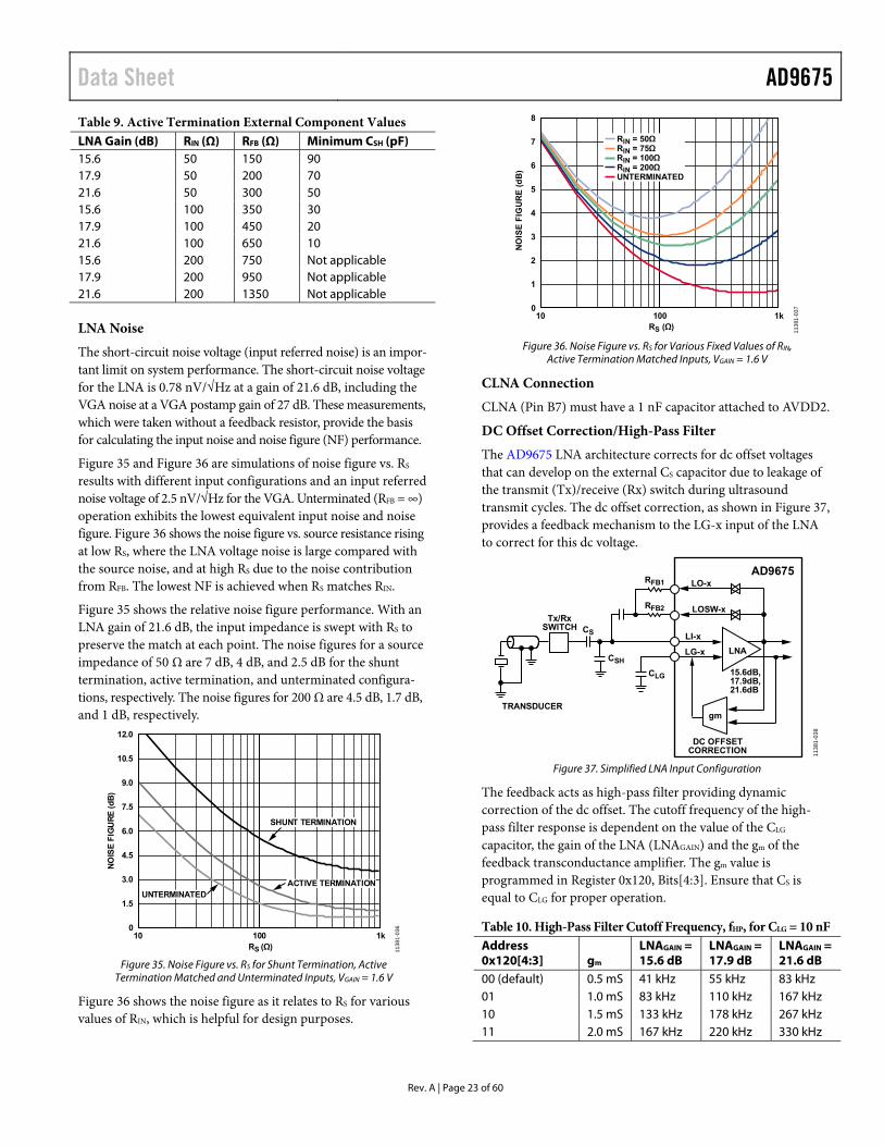
Table 9. Active Termination External Component Values LNA Gain (dB) RIN (Ω) RFB (Ω) Minimum CSH (pF) 15.6 50 150 90 17.9 50 200 70 21.6 50 300 50 15.6 100 350 30 17.9 100 450 20 21.6 100 650 10 15.6 200 750 Not applicable 17.9 200 950 Not applicable 21.6 200 1350 Not applicable
LNA Noise
The short-circuit noise voltage (input referred noise) is an impor-tant limit on system performance. The short-circuit noise voltage for the LNA is 0.78 nV/√Hz at a gain of 21.6 dB, including the VGA noise at a VGA postamp gain of 27 dB. These measurements, which were taken without a feedback resistor, provide the basis for calculating the input noise and noise figure (NF) performance.
Figure 35 and Figure 36 are simulations of noise figure vs. RS results with different input configurations and an input referred noise voltage of 2.5 nV/√Hz for the VGA. Unterminated (RFB = ∞) operation exhibits the lowest equivalent input noise and noise figure. Figure 36 shows the noise figure vs. source resistance rising at low RS, where the LNA voltage noise is large compared with the source noise, and at high RS due to the noise contribution from RFB. The lowest NF is achieved when RS matches RIN.
Figure 35 shows the relative noise figure performance. With an LNA gain of 21.6 dB, the input impedance is swept with RS to preserve the match at each point. The noise figures for a source impedance of 50 Ω are 7 dB, 4 dB, and 2.5 dB for the shunt termination, active termination, and unterminated configura-tions, respectively. The noise figures for 200 Ω are 4.5 dB, 1.7 dB, and 1 dB, respectively.
Figure 35. Noise Figure vs. RS for Shunt Termination, Active
Termination Matched and Unterminated Inputs, VGAIN = 1.6 V
Figure 36 shows the noise figure as it relates to RS for various values of RIN, which is helpful for design purposes.
Figure 36. Noise Figure vs. RS for Various Fixed Values of RIN,
Active Termination Matched Inputs, VGAIN = 1.6 V
CLNA Connection
CLNA (Pin B7) must have a 1 nF capacitor attached to AVDD2.
DC Offset Correction/High-Pass Filter
The AD9675 LNA architecture corrects for dc offset voltages that can develop on the external CS capacitor due to leakage of the transmit (Tx)/receive (Rx) switch during ultrasound transmit cycles. The dc offset correction, as shown in Figure 37, provides a feedback mechanism to the LG-x input of the LNA to correct for this dc voltage.
Figure 37. Simplified LNA Input Configuration
The feedback acts as high-pass filter providing dynamic correction of the dc offset. The cutoff frequency of the high-pass filter response is dependent on the value of the CLG capacitor, the gain of the LNA (LNAGAIN) and the gm of the feedback transconductance amplifier. The gm value is programmed in Register 0x120, Bits[4:3]. Ensure that CS is equal to CLG for proper operation.
Table 10. High-Pass Filter Cutoff Frequency, fHP, for CLG = 10 nF Address 0x120[4:3] gm
LNAGAIN = 15.6 dB
LNAGAIN = 17.9 dB
LNAGAIN = 21.6 dB
00 (default) 0.5 mS 41 kHz 55 kHz 83 kHz 01 1.0 mS 83 kHz 110 kHz 167 kHz 10 1.5 mS 133 kHz 178 kHz 267 kHz 11 2.0 mS 167 kHz 220 kHz 330 kHz
10 100 1k0
1.5
3.0
4.5
6.0
7.5
9.0
10.5
12.0
RS (Ω)
NO
ISE
FIG
UR
E(d
B)
UNTERMINATEDACTIVE TERMINATION
SHUNT TERMINATION
1138
1-03
6
10 100 1k0
1
2
3
4
5
6
7
8
RS (Ω)
NO
ISE
FIG
UR
E (
dB
)
RIN = 50ΩRIN = 75ΩRIN = 100ΩRIN = 200ΩUNTERMINATED
1138
1-03
7
LNA
LOSW-x
LO-x
LI-x
LG-x
RFB2
RFB1
CLG
CSH
TRANSDUCER
CS
Tx/RxSWITCH
15.6dB,17.9dB,21.6dB
AD9675
DC OFFSETCORRECTION
gm
1138
1-03
8

AD9675 Data Sheet
Rev. A | Page 24 of 60
For other values of CLG, determine the high-pass filter cutoff frequency by scaling the values from Table 10 or calculating based on CLG, LNAGAIN, and gm, as shown in Equation 6.
LGHP
LG
mGAINLGHP C
fCgLNACf
nF102
1)(
(6)
where fHP is the high-pass filter cutoff frequency (see Table 10).
Variable Gain Amplifier (VGA)
The differential X-AMP VGA provides precise input attenu-ation and interpolation. It has a low input referred noise of 2.5 nV/√Hz and excellent gain linearity. The VGA is driven by a fully differential input signal from the LNA. The X-AMP archi-tecture produces a linear-in-dB gain law conformance and low distortion levels—deviating only ±0.5 dB or less from the ideal. The gain slope is monotonic with respect to the control voltage and is stable with variations in process, temperature, and supply. The resulting total gain range is 45 dB, which allows range loss at the endpoints.
The X-AMP inputs are part of a PGA that completes the VGA. The PGA in the VGA can be programmed to a gain of 21 dB, 24 dB, 27 dB, or 30 dB, allowing for optimization of channel gain for different imaging modes in the ultrasound system. The VGA bandwidth is greater than 100 MHz. The input stage ensures excellent frequency response uniformity across the gain setting. For TGC mode, this minimizes time delay variation across the gain range.
Gain Control
The analog gain control interface, GAIN±, is a differential input. VGAIN varies the gain of all VGAs through the interpolator by selecting the appropriate input stages connected to the input attenuator. The nominal VGAIN range is 14 dB/V from −1.6 V to +1.6 V, with the best gain linearity from approximately −1.44 V to +1.44 V, where the error is typically less than ±0.5 dB. For VGAIN voltages of greater than 1.44 V and less than −1.44 V, the error increases. The value of GAIN± can exceed the supply voltage by 1 V without gain foldover.
Gain control response time is less than 750 ns to settle within 10% of the final value for a change from minimum to maximum gain.
The differential input pins, GAIN+ and GAIN−, can interface to an amplifier, as shown in Figure 38. Decouple and drive the GAIN+ and GAIN− pins to accommodate a 3.2 V full-scale input.
Figure 38. Differential GAIN± Pin Configuration
Use Address 0x011, Bits[7:4], to disable the analog gain control and to control the attenuator digitally. The control range is 45 dB and the step size is 3.5 dB.
VGA Noise
In a typical application, a VGA compresses a wide dynamic range input signal to within the input span of an ADC. The input referred noise of the LNA limits the minimum resolvable input signal, whereas the output referred noise, which depends primarily on the VGA, limits the maximum instantaneous dynamic range that can be processed at any one particular gain control voltage. This latter limit is set in accordance with the total noise floor of the ADC.
The output referred noise is a flat 40 nV/√Hz (postamp gain = 24 dB) over most of the gain range because it is dominated by the fixed output referred noise of the VGA. At the high end of the gain control range, the noise of the LNA and the source prevail. The input referred noise reaches its minimum value near the maximum gain control voltage, where the input referred contribution of the VGA is miniscule.
At lower gains, the input referred noise and, therefore, the noise figure increase as the gain decreases. The instantaneous dynamic range of the system is not lost, however, because the input capacity increases as the input referred noise increases. The contribution of the ADC noise floor has the same dependence. The important relationship is the magnitude of the VGA output noise floor relative to that of the ADC.
Gain control noise is a concern in very low noise applications. Thermal noise in the gain control interface can modulate the channel gain. The resulting noise is proportional to the output signal level and is usually evident only when a large signal is present. Take care to minimize noise impinging at the GAIN± inputs. Use an external RC filter to remove VGAIN source noise. Ensure that the filter bandwidth is sufficient to accommodate the desired control bandwidth and attenuate unwanted switching noise from the external DACs used to drive the gain control.
The AD9675 can bypass the GAIN± inputs and control the gain of the attenuator digitally (see the Gain Control section). This mode removes any external noise contributions when active gain control is not needed.
Antialiasing Filter (AAF)
The filter that the signal reaches prior to the ADC is used to reject dc signals and to band limit the signal for antialiasing. The antialiasing filter is a combination of a single-pole, high-pass filter and a second-order, low-pass filter. Configure the high-pass filter as a ratio of the low-pass filter cutoff frequency using Address 0x02B, Bits[1:0].
The filter uses on-chip tuning to trim the capacitors and, in turn, to set the desired low-pass cutoff frequency and reduce variations. The default −3 dB low-pass filter cutoff is 1/3, 1/4.5, or 1/6 of the ADC sample clock rate. The cutoff can be scaled to 0.75, 0.8, 0.9, 1.0, 1.13, 1.25, or 1.45 times this frequency using Address 0x00F. The cutoff tolerance (±10%) is maintained from 8 MHz to 18 MHz for low bandwidth mode or 13.5 MHz to 30 MHz for high bandwidth mode.
ADA4938-1ADA4938-2
249Ω
AD9675
249Ω
±0.8V DCAT 0.8V CM
±0.8V DCAT 0.8V CM
±1.6V249Ω
0.8V CM
249Ω
100Ω
0.01µFGAIN+
GAIN–0.01µF
100Ω
31.3kΩ
10kΩ
1138
1-03
9

Data Sheet AD9675
Rev. A | Page 25 of 60
Table 11 and Table 12 calculate the valid SPI-selectable low-pass filter settings and expected cutoff frequencies for the low bandwidth and high bandwidth modes at the minimum sample frequency and the maximum sample frequency in each speed mode.
Tuning is normally off to avoid changing the capacitor settings during critical times. The tuning circuit is enabled through the SPI. It is disabled automatically after 512 cycles of the ADC sample clock. Initialize the tuning of the filter after initial power-up and
after reprogramming of the filter cutoff scaling or the ADC sample rate. The tuning is initiated using Address 0x02B, Bit 6.
Four SPI-programmable settings allow users to vary the high-pass filter cutoff frequency as a function of the low-pass cutoff frequency. Two examples are shown in Table 13: an 8 MHz low-pass cutoff frequency and an 18 MHz low-pass cutoff frequency. In both cases, as the ratio decreases, the amount of rejection on the low end frequencies increases. Therefore, making the entire AAF frequency pass band narrow can reduce low frequency noise or maximize dynamic range for harmonic processing.
Table 11. SPI-Selectable Low-Pass Filter Cutoff Options for Low Bandwidth Mode at Example Sampling Frequencies
Address 0x00F[7:3]
LPF Cutoff Frequency (MHz)
Sampling Frequency (MHz) 20.5 40 65 80 125
0 0000 1.45 × (1/3) × fSAMPLE 9.91 Out of tunable filter range
Out of tunable filter range
Out of tunable filter range
Out of tunable filter range
0 0001 1.25 × (1/3) × fSAMPLE 8.54 16.67 Out of tunable filter range
Out of tunable filter range
Out of tunable filter range
0 0010 1.13 × (1/3) × fSAMPLE Out of tunable filter range
15.00 Out of tunable filter range
Out of tunable filter range
Out of tunable filter range
0 0011 1.0 × (1/3) × fSAMPLE Out of tunable filter range
13.33 Out of tunable filter range
Out of tunable filter range
Out of tunable filter range
0 0100 0.9 × (1/3) × fSAMPLE Out of tunable filter range
12.00 Out of tunable filter range
Out of tunable filter range
Out of tunable filter range
0 0101 0.8 × (1/3) × fSAMPLE Out of tunable filter range
10.67 17.33 Out of tunable filter range
Out of tunable filter range
0 0110 0.75 × (1/3) × fSAMPLE Out of tunable filter range
10.00 16.25 16.82 Out of tunable filter range
0 1000 1.45 × (1/4.5) × fSAMPLE Out of tunable filter range
12.89 20.94 Out of tunable filter range
Out of tunable filter range
0 1001 1.25 × (1/4.5) × fSAMPLE Out of tunable filter range
11.11 18.06 Out of tunable filter range
Out of tunable filter range
0 1010 1.13 × (1/4.5) × fSAMPLE Out of tunable filter range
10.00 16.25 Out of tunable filter range
Out of tunable filter range
0 1011 1.0 × (1/4.5) × fSAMPLE Out of tunable filter range
8.89 14.44 17.78 Out of tunable filter range
0 1100 0.9 × (1/4.5) × fSAMPLE Out of tunable filter range
8.00 13.00 16.00 Out of tunable filter range
0 1101 0.8 × (1/4.5) × fSAMPLE Out of tunable filter range
Out of tunable filter range
11.56 14.22 Out of tunable filter range
0 1110 0.75 × (1/4.5) × fSAMPLE Out of tunable filter range
Out of tunable filter range
10.83 13.33 17.50
1 0000 1.45 × (1/6) × fSAMPLE Out of tunable filter range
9.67 15.71 Out of tunable filter range
Out of tunable filter range
1 0001 1.25 × (1/6) × fSAMPLE Out of tunable filter range
8.33 13.54 16.67 Out of tunable filter range
1 0010 1.13 × (1/6) × fSAMPLE Out of tunable filter range
Out of tunable filter range
12.19 15.00 Out of tunable filter range
1 0011 1.0 × (1/6) × fSAMPLE Out of tunable filter range
Out of tunable filter range
10.83 13.33 Out of tunable filter range
1 0100 0.9 × (1/6) × fSAMPLE Out of tunable filter range
Out of tunable filter range
9.75 12.00 Out of tunable filter range
1 0101 0.8 × (1/6) × fSAMPLE Out of tunable filter range
Out of tunable filter range
8.67 10.67 16.67
1 0110 0.75 × (1/6) × fSAMPLE Out of tunable filter range
Out of tunable filter range
8.13 10.00 15.63

AD9675 Data Sheet
Rev. A | Page 26 of 60
Table 12. SPI-Selectable Low-Pass Filter Cutoff Options for High Bandwidth Mode at Example Sampling Frequencies
Address 0x00F[7:3]
LPF Cutoff Frequency (MHz)
Sampling Frequency (MHz) 20.5 40 65 80 125
0 0000 1.45 × (1/3) × fSAMPLE Out of tunable filter range
19.33 Out of tunable filter range
Out of tunable filter range
Out of tunable filter range
0 0001 1.25 × (1/3) × fSAMPLE Out of tunable filter range
16.67 27.08 Out of tunable filter range
Out of tunable filter range
0 0010 1.13 × (1/3) × fSAMPLE Out of tunable filter range
15.00 24.38 30.00 Out of tunable filter range
0 0011 1.0 × (1/3) × fSAMPLE Out of tunable filter range
Out of tunable filter range
21.67 26.67 Out of tunable filter range
0 0100 0.9 × (1/3) × fSAMPLE Out of tunable filter range
Out of tunable filter range
19.50 24.00 Out of tunable filter range
0 0101 0.8 × (1/3) × fSAMPLE Out of tunable filter range
Out of tunable filter range
17.33 21.33 Out of tunable filter range
0 0110 0.75 × (1/3) × fSAMPLE Out of tunable filter range
Out of tunable filter range
16.25 20.00 Out of tunable filter range
0 1000 1.45 × (1/4.5) × fSAMPLE Out of tunable filter range
Out of tunable filter range
20.94 25.78 Out of tunable filter range
0 1001 1.25 × (1/4.5) × fSAMPLE Out of tunable filter range
Out of tunable filter range
18.06 22.22 Out of tunable filter range
0 1010 1.13 × (1/4.5) × fSAMPLE Out of tunable filter range
Out of tunable filter range
16.25 20.00 Out of tunable filter range
0 1011 1.0 × (1/4.5) × fSAMPLE Out of tunable filter range
Out of tunable filter range
14.44 17.78 27.78
0 1100 0.9 × (1/4.5) × fSAMPLE Out of tunable filter range
Out of tunable filter range
Out of tunable filter range
16.00 25.00
0 1101 0.8 × (1/4.5) × fSAMPLE Out of tunable filter range
Out of tunable filter range
Out of tunable filter range
14.22 22.22
0 1110 0.75 × (1/4.5) × fSAMPLE Out of tunable filter range
Out of tunable filter range
Out of tunable filter range
Out of tunable filter range
20.83
1 0000 1.45 × (1/6) × fSAMPLE Out of tunable filter range
Out of tunable filter range
15.71 19.33 Out of tunable filter range
1 0001 1.25 × (1/6) × fSAMPLE Out of tunable filter range
Out of tunable filter range
13.54 16.67 26.04
1 0010 1.13 × (1/6) × fSAMPLE Out of tunable filter range
Out of tunable filter range
Out of tunable filter range
15.00 23.44
1 0011 1.0 × (1/6) × fSAMPLE Out of tunable filter range
Out of tunable filter range
Out of tunable filter range
Out of tunable filter range
20.83
1 0100 0.9 × (1/6) × fSAMPLE Out of tunable filter range
Out of tunable filter range
Out of tunable filter range
Out of tunable filter range
18.75
1 0101 0.8 × (1/6) × fSAMPLE Out of tunable filter range
Out of tunable filter range
Out of tunable filter range
Out of tunable filter range
16.67
1 0110 0.75 × (1/6) × fSAMPLE Out of tunable filter range
Out of tunable filter range
Out of tunable filter range
Out of tunable filter range
15.63
Table 13. High-Pass Filter Cutoff Options
Address 0x02B[1:0] High-Pass Filter Cutoff
High-Pass Cutoff Frequency Ratio1 Low-Pass Cutoff = 8 MHz Low-Pass Cutoff = 18 MHz
00 (default) 12.00 670 kHz 1.5 MHz 01 9.00 890 kHz 2.0 MHz 10 6.00 1.33 MHz 3.0 MHz 11 3.00 2.67 MHz 6.0 MHz 1 Ratio is the low-pass filter cutoff frequency/high-pass filter cutoff frequency.

Data Sheet AD9675
Rev. A | Page 27 of 60
AAF/VGA Test Mode
For debug and testing, there is a bypass switch to view the AAF output on the GPO2 and GPO3 pins. Enable this mode via SPI Address 0x109, Bit 4. The differential AAF output of only one channel can be accessed at a time. The dc output voltage is 1.5 V (or AVDD2/2) and the maximum ac output voltage is 2 V p-p.
ADC
The AD9675 uses a pipelined ADC architecture. The quantized output from each stage is combined into a 14-bit result in the digital correction logic. The pipelined architecture permits the first stage to operate on a new input sample and the remaining stages to operate on preceding samples. Sampling occurs on the rising edge of the clock.
The output staging block aligns the data, corrects errors, and passes the data to the output buffers. The data is then serialized and aligned to the frame and output clocks.
Clock Input Considerations
For optimum performance, clock the AD9675 sample clock inputs (CLK+ and CLK−) with a differential signal. This signal is typically ac-coupled into the CLK+ and CLK− pins via a transformer or capacitors. These pins are biased internally and require no additional bias.
Figure 39 shows the preferred method for clocking the AD9675. A low jitter clock source, such as the Valpey Fisher oscillator, VFAC3AHL-1 80.000, is converted from single-ended to differential using an RF transformer. The back-to-back Schottky diodes across the secondary transformer limit clock excursions into the AD9675 to approximately 0.8 V p-p differential. This prevents the large voltage swings of the clock from feeding through to other portions of the AD9675, and it preserves the fast rise and fall times of the signal, which are critical to low jitter performance.
Figure 39. Transformer-Coupled Differential Clock
If a low jitter clock is available, another option is to ac couple a differential positive emitter-coupled logic (PECL) signal to the sample clock input pins, as shown in Figure 40. Analog Devices offers clock drivers with excellent jitter performance, such as the AD9516-0 or the AD9524.
Figure 40. Differential PECL Sample Clock
A third option is to ac couple a differential LVDS signal to the sample clock input pins, as shown in Figure 41.
Figure 41. Differential LVDS Sample Clock
In some applications, it is acceptable to drive the sample clock inputs with a single-ended CMOS signal. In such applications, drive CLK+ directly from a CMOS gate, and bypass the CLK− pin to ground with a 0.1 μF capacitor (see Figure 42).
Figure 42. Single-Ended 1.8 V CMOS Sample Clock
Clock Duty Cycle Considerations
Typical high speed ADCs use both clock edges to generate a variety of internal timing signals. As a result, these ADCs can be sensitive to the clock duty cycle. Commonly, a 5% tolerance is required on the clock duty cycle to maintain dynamic performance characteristics. The AD9675 contains a duty cycle stabilizer (DCS) that retimes the nonsampling edge, providing an internal clock signal with a nominal 50% duty cycle. This allows a wide range of clock input duty cycles without affecting the performance of the AD9675. When the DCS is on, noise and distortion performance are nearly flat for a wide range of duty cycles. However, some applications may require the DCS function to be off. When the DCS function is off, the dynamic range performance can be affected.
The duty cycle stabilizer uses a delay-locked loop (DLL) to create the nonsampling edge. As a result, any changes to the sampling frequency require approximately eight clock cycles to allow the DLL to acquire and lock to the new rate.
0.1µF
0.1µF
0.1µF0.1µF
SCHOTTKYDIODES:HSM2812
3.3V
50Ω100Ω
CLK–
CLK+
ADC
MINI-CIRCUITS®
ADT1-1WT, 1:1Z
XFMR
VFAC3
OUT
1138
1-04
0
100Ω
0.1µF
0.1µF0.1µF
0.1µF
240Ω240Ω
AD9524/AD9516-0
CLK
CLK
*50Ω RESISTOR IS OPTIONAL.
PECL DRIVER
3.3V
OUT
VFAC3
CLK–
CLK+
ADC50Ω*
1138
1-04
1
100Ω0.1µF
0.1µF0.1µF
0.1µF
AD9524/AD9516-0
CLK
CLK
*50Ω RESISTOR IS OPTIONAL.
LVDS DRIVER
3.3V
OUT
VFAC3
CLK–
CLK+
ADC50Ω*
1138
1-04
2
0.1µFOPTIONAL
100Ω
0.1µF
0.1µF
CMOS DRIVER
0.1µFCLK
CLK
*50Ω RESISTOR IS OPTIONAL.
AD9524/AD9516-0
3.3V
OUT
VFAC3
CLK–
CLK+
ADC
50Ω*
1138
1-04
3

AD9675 Data Sheet
Rev. A | Page 28 of 60
Clock Jitter Considerations
High speed, high resolution ADCs are sensitive to the quality of the clock input. Calculate the degradation in SNR at a given input frequency (fA) due only to aperture jitter (tJ) as follows:
SNR Degradation = 20 × log 10(1/2 × π × fA × tJ) (7)
In this equation, the rms aperture jitter represents the root mean square of all jitter sources, including the clock input, analog input signal, and ADC aperture jitter (see Figure 43).
Treat the clock input as an analog signal in cases where aperture jitter may affect the dynamic range of the AD9675. Separate power supplies for clock drivers from the ADC output driver supplies to avoid modulating the clock signal with digital noise. Low jitter, crystal controlled oscillators make the best clock sources, such as the Valpey Fisher VFAC3 series. If the clock is generated from another type of source (by gating, dividing, or other methods), it is retimed by the original clock during the last step.
For more information on how jitter performance relates to ADCs, refer to the AN-501 Application Note and the AN-756 Application Note.
Figure 43. Ideal SNR vs. Input Frequency and Jitter
Power Dissipation and Power-Down Mode
The power dissipated by the AD9675 is proportional to its sample rate. The digital power dissipation does not vary significantly because it is determined primarily by the DRVDD supply and the bias current of the LVDS output drivers. The AD9675 features scalable LNA bias currents (see Table 31, Address 0x012). The default LNA bias current settings are midhigh.
By asserting the PDWN pin high, the AD9675 is placed into power-down mode. In this state, the device typically dissipates 5 mW. During power-down, the LVDS output drivers are placed into a high impedance state. The AD9675 returns to normal operating mode when the PDWN pin is pulled low. This pin is only 1.8 V tolerant. To drive the PDWN pin from a 3.3 V logic level, insert a 1 kΩ resistor in series with this pin to limit the current.
By asserting the STBY pin high, the AD9675 is placed in standby mode. In this state, the device typically dissipates 725 mW. During standby, the entire device is powered down except the internal references. The LVDS output drivers are placed into a high impedance state. This mode is well suited for applications that require power savings because it allows the device to be powered down when not in use and then quickly powers up. The time to power up the device is also greatly reduced. The AD9675 returns to normal operating mode when the STBY pin is pulled low. This pin is only 1.8 V tolerant. To drive the STBY pin from a 3.3 V logic level, insert a 1 kΩ resistor in series with this pin to limit the current.
In power-down mode, low power dissipation is achieved by shutting down the reference, reference buffer, PLL, and biasing networks. The decoupling capacitors on VREF are discharged when entering power-down mode and must be recharged when returning to normal operation. As a result, the wake-up time is related to the time spent in power-down mode: shorter cycles result in proportionally shorter wake-up times. To restore the device to full operation, approximately 375 μs is required when using the recommended 1 μF and 0.1 μF decoupling capacitors on the VREF pin and the 0.01 μF decoupling capacitors on the GAIN± pins. Most of this time is dependent on gain decoupling; higher value decoupling capacitors on the GAIN± pins result in longer wake-up times.
A number of other power-down options are available when using the SPI port interface. The user can individually power down each channel or place the entire device into standby mode. When fast wake-up times are required, standby mode allows the user to keep the internal PLL powered up. The wake-up time is slightly dependent on gain. To achieve a 2 μs wake-up time when the device is in standby mode, apply 0.8 V to the GAIN± pins.
Power and Ground Connection Recommendations
When connecting power to the AD9675, use two separate 1.8 V supplies: one for analog (AVDD1) and one for digital (DRVDD). If only one 1.8 V supply is available, route it to the AVDD1 pin first and then tap it off and isolate it with a ferrite bead or a filter choke preceded by decoupling capacitors for the DRVDD pin.
The DVDD pin can be tied to the 1.8 V DRVDD supply. When this is done, route the DVDD supply first, tap it off, and isolate it with a ferrite bead or filter choke preceded by decoupling capacitors for the DRVDD pin. It is not recommended to use the same supply for AVDD1, DVDD, and DRVDD. For compatibility with the AD9671 or for lower power operation, the DVDD pin can be tied to 1.4 V.
For both high and low frequencies, use several decoupling capacitors on all supplies. Place these capacitors near the point of entry at the PCB level and near the device, with minimal trace lengths.
When using the AD9675, a single PCB ground plane is sufficient. With proper decoupling and smart partitioning of the analog,
1 10 100 1000
16 BITS
14 BITS
12 BITS
30
40
50
60
70
80
90
100
110
120
130
0.125ps
0.5ps1.0ps2.0ps
ANALOG INPUT FREQUENCY (MHz)
10 BITS
8 BITS
RMS CLOCK JITTER REQUIREMENT
SN
R(d
B)
0.25ps
1138
1-04
4

Data Sheet AD9675
Rev. A | Page 29 of 60
digital, and clock sections of the PCB, optimum performance can be easily achieved.
Advanced Power Control
For an ultrasound system, not all channels are needed during all scanning periods. The POWER_START and POWER_STOP values in the vector profile can be used to delay the channel startup and turn the channel off after a certain number of samples. These counters are relative to TX_TRIG±. The analog circuitry needs to power up before the digital one and the advance time (POWER_SETUP) for powering up the analog circuitry, before POWER_START, is set up in Address 0x112 (see Table 31).
Figure 44. Power Sequencing
DIGITAL OUTPUTS AND TIMING JESD204B Transmit Top Level Description
The AD9675 digital output complies with the JEDEC Standard JESD204B, Serial Interface for Data Converters. JESD204B is a protocol to link the AD9675 to a digital processing device over
a serial interface up to 5 Gbps link speeds. The benefits of the JESD204B interface include a reduction in required board area for data interface routing, and enables smaller packages for converter and logic devices. The AD9675 supports single, dual, or quad lane interfaces.
JESD204B Overview
The JESD204B data transmit block, as shown in Figure 45, assembles the parallel channel data from the ADC or digital processing block into frames and uses 8-bit/10-bit encoding as well as optional scrambling to form serial output data. Lane synchronization is supported through the use of special characters during the initial establishment of the link, and additional synchronization is embedded in the data stream thereafter. A matching external receiver is required to lock onto the serial data stream and recover the data and clock. For additional details on the JESD204B interface, users are encouraged to refer to the JESD204B standard.
The AD9675 JESD204B transmit block maps the eight channel outputs over a link. A link can be configured to use either single, dual, or quad serial differential outputs, which are called lanes. The JESD204B specification refers to a number of parameters to define the link, and these parameters must match between the JESD204B transmitter (AD9675 output) and receiver.
The JESD204B link is described according to the parameters listed in Table 14.
Table 14. JESD204B Parameters Parameter Description AD9675 Value S Samples transmitted per single converter per frame cycle 1 M Number of converters per converter device 8 L Number of lanes per converter device 1, 2, or 4 N Converter resolution 12, 14, or 16 N' Total number of bits per sample 16 CF Number of control words per frame clock cycle per
converter device 0
CS Number of control bits per conversion sample 0 K Number of frames per multiframe Configurable on the AD9675 HD High density mode 0 F Octets per frame 4, 8, 16, or 32 (dependent on L = 4, 2, or 1, respectively) C Control bit 0 T Tail bit Available on the AD9675 SCR Scrambler enable/disable Configurable on the AD9675 FCHK Checksum for the JESD204B parameters Automatically calculated and stored in the register map
TX_TRIG±POWER_STOP
(PROFILE SPECIFIC)
POWER_START(PROFILE SPECIFIC)
POWER_SETUP(SPI SET)
DIGITALPOWER
ANALOGPOWER
1138
1-04
5
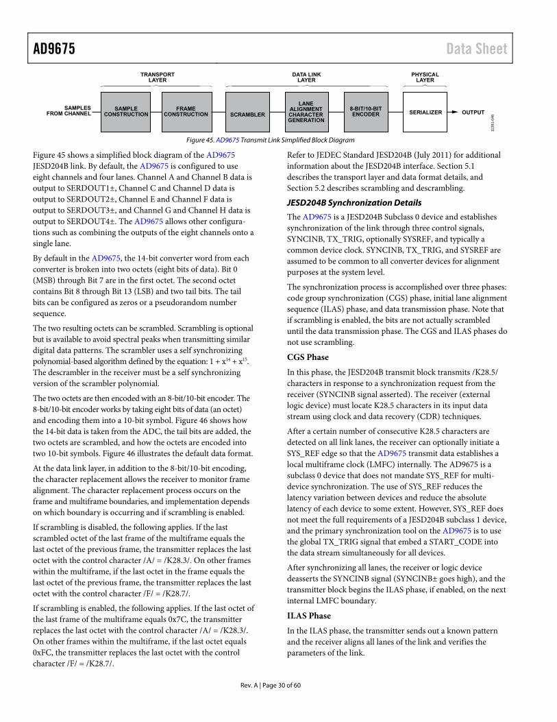
AD9675 Data Sheet
Rev. A | Page 30 of 60
Figure 45. AD9675 Transmit Link Simplified Block Diagram
Figure 45 shows a simplified block diagram of the AD9675 JESD204B link. By default, the AD9675 is configured to use eight channels and four lanes. Channel A and Channel B data is output to SERDOUT1±, Channel C and Channel D data is output to SERDOUT2±, Channel E and Channel F data is output to SERDOUT3±, and Channel G and Channel H data is output to SERDOUT4±. The AD9675 allows other configura-tions such as combining the outputs of the eight channels onto a single lane.
By default in the AD9675, the 14-bit converter word from each converter is broken into two octets (eight bits of data). Bit 0 (MSB) through Bit 7 are in the first octet. The second octet contains Bit 8 through Bit 13 (LSB) and two tail bits. The tail bits can be configured as zeros or a pseudorandom number sequence.
The two resulting octets can be scrambled. Scrambling is optional but is available to avoid spectral peaks when transmitting similar digital data patterns. The scrambler uses a self synchronizing polynomial-based algorithm defined by the equation: 1 + x14 + x15. The descrambler in the receiver must be a self synchronizing version of the scrambler polynomial.
The two octets are then encoded with an 8-bit/10-bit encoder. The 8-bit/10-bit encoder works by taking eight bits of data (an octet) and encoding them into a 10-bit symbol. Figure 46 shows how the 14-bit data is taken from the ADC, the tail bits are added, the two octets are scrambled, and how the octets are encoded into two 10-bit symbols. Figure 46 illustrates the default data format.
At the data link layer, in addition to the 8-bit/10-bit encoding, the character replacement allows the receiver to monitor frame alignment. The character replacement process occurs on the frame and multiframe boundaries, and implementation depends on which boundary is occurring and if scrambling is enabled.
If scrambling is disabled, the following applies. If the last scrambled octet of the last frame of the multiframe equals the last octet of the previous frame, the transmitter replaces the last octet with the control character /A/ = /K28.3/. On other frames within the multiframe, if the last octet in the frame equals the last octet of the previous frame, the transmitter replaces the last octet with the control character /F/ = /K28.7/.
If scrambling is enabled, the following applies. If the last octet of the last frame of the multiframe equals 0x7C, the transmitter replaces the last octet with the control character /A/ = /K28.3/. On other frames within the multiframe, if the last octet equals 0xFC, the transmitter replaces the last octet with the control character /F/ = /K28.7/.
Refer to JEDEC Standard JESD204B (July 2011) for additional information about the JESD204B interface. Section 5.1 describes the transport layer and data format details, and Section 5.2 describes scrambling and descrambling.
JESD204B Synchronization Details
The AD9675 is a JESD204B Subclass 0 device and establishes synchronization of the link through three control signals, SYNCINB, TX_TRIG, optionally SYSREF, and typically a common device clock. SYNCINB, TX_TRIG, and SYSREF are assumed to be common to all converter devices for alignment purposes at the system level.
The synchronization process is accomplished over three phases: code group synchronization (CGS) phase, initial lane alignment sequence (ILAS) phase, and data transmission phase. Note that if scrambling is enabled, the bits are not actually scrambled until the data transmission phase. The CGS and ILAS phases do not use scrambling.
CGS Phase
In this phase, the JESD204B transmit block transmits /K28.5/ characters in response to a synchronization request from the receiver (SYNCINB signal asserted). The receiver (external logic device) must locate K28.5 characters in its input data stream using clock and data recovery (CDR) techniques.
After a certain number of consecutive K28.5 characters are detected on all link lanes, the receiver can optionally initiate a SYS_REF edge so that the AD9675 transmit data establishes a local multiframe clock (LMFC) internally. The AD9675 is a subclass 0 device that does not mandate SYS_REF for multi-device synchronization. The use of SYS_REF reduces the latency variation between devices and reduce the absolute latency of each device to some extent. However, SYS_REF does not meet the full requirements of a JESD204B subclass 1 device, and the primary synchronization tool on the AD9675 is to use the global TX_TRIG signal that embed a START_CODE into the data stream simultaneously for all devices.
After synchronizing all lanes, the receiver or logic device deasserts the SYNCINB signal (SYNCINB± goes high), and the transmitter block begins the ILAS phase, if enabled, on the next internal LMFC boundary.
ILAS Phase
In the ILAS phase, the transmitter sends out a known pattern and the receiver aligns all lanes of the link and verifies the parameters of the link.
OUTPUTSAMPLES
FROM CHANNEL
TRANSPORTLAYER
DATA LINKLAYER
PHYSICALLAYER
SCRAMBLER SERIALIZERFRAME
CONSTRUCTION8-BIT/10-BITENCODER
SAMPLECONSTRUCTION
LANEALIGNMENTCHARACTERGENERATION
1138
1-04
6

Data Sheet AD9675
Rev. A | Page 31 of 60
The ILAS phase begins after SYNCINB± is deasserted (goes high). The transmit block begins to transmit four multiframes. Dummy samples are inserted between the required characters so that full multiframes are transmitted.
The four multiframes have the following properties:
Multiframe 1 begins with an /R/ character (K28.0) and ends with an /A/ character (K28.3).
Multiframe 2 begins with an /R/ character, followed by a /Q/ (K28.4) character and link configuration parameters over 14 configuration octets (see Table 15), and ends with an /A/ character. Many of the parameter values are of the notation of the value − 1.
Multiframe 3 is the same as Multiframe 1. Multiframe 4 is the same as Multiframe 1.
Data Transmission Phase
By the end of the ILAS phase, data transmission starts. Initiating a global TX_TRIG signal resets any sampling edges within the ADC and replaces a sample with the START_CODE (see Address 0x18B and Address 0x18C in Table 31). Aligning the data on all lanes based on the START_CODE guarantees the synchronization across multiple lanes and across multiple devices.
In the data transmission phase, frame alignment is monitored with control characters. Character replacement is used at the end of frames. Character replacement in the transmitter occurs in the following instances:
If scrambling is disabled and the last octet of the frame or multiframe equals the octet value of the previous frame.
If scrambling is enabled and the last octet of the multiframe is equal to 0x7C, or the last octet of a frame is equal to 0xFC.
Table 15. 14 Configuration Octets of the ILAS Phase
No. Bit 7 (MSB)
Bit 6
Bit 5
Bit 4
Bit 3
Bit 2
Bit 1
Bit 0 (LSB)
0 DID[7:0] 1 0 0 0 0 BID[3:0] 2 0 0 0 LID[4:0] 3 SCR 0 0 L[4:0] 4 F[7:0] 5 0 0 0 K[4:0] 6 M[7:0] 7 CS[1:0] 0 N[4:0] 8 0 0 0 N'[4:0] 9 0 0 0 S[4:0] 10 HD 0 0 CF[4:0] 11 Reserved, don’t care 12 Reserved, don’t care 13 FCHK[7:0]
Link Setup Parameters
The following steps demonstrate how to configure the AD9675 JESD204B interface and the outputs.
1. Disable lanes before changing the configuration 2. Select the converter and lane configuration 3. Configure the tail bits and control bits 4. Set the lane identification values 5. Set the number of frame per multiframe, K 6. Enable scramble, SCR 7. Set the lane synchronization options 8. Check FCHK, checksum of JESD204B interface parameters 9. Set additional digital output configuration options 10. Reenable lane(s) after configuration
Disable Lanes
Before modifying the JESD204B link parameters, disable the link and hold it in reset. This is accomplished by writing a Logic 1 to Address 0x142, Bit 0.
Converter and Lane Configuration
The JESD204B M parameter (number of converters) is set to 8 (Address 0x153 = 0x07).
The lane configuration is set in Address 0x150, Bits[1:0] such that 00 = one lane per link, 01 = two lanes per link, or 11 = four lanes per link. The channel data (A to H) is placed on the JESD204B lanes according Table 16.
Table 16. Channel to JESD204B Lane Mapping L SERDOUT1± SERDOUT2± SERDOUT3± SERDOUT4± 1 A, B, C, D, E, F,
G, H Power-down Power-down Power-down
2 A, B, C, D Power-down E, F, G, H Power-down 4 A, B C, D E, F G, H
Configure the Tail Bits and Control Bits
With N' = 16 and N = 14, two tail bits are available per sample for transmitting additional information over the JESD204B link. Tail bits are dummy bits sent over the link to complete the two octets and do not convey any information about the input signal. Tail bits can be fixed zeros (default) or pseudorandom numbers (Address 0x142, Bit 6).
Set Lane Identification Values
JESD204B allows parameters to identify the device and lane. These parameters are transmitted during the ILAS phase, and they are accessible in the internal registers.
There are three identification values: device identification (DID), bank identification (BID), and lane identification (LID). DID and BID are device specific; therefore, they can be used for link identification.

AD9675 Data Sheet
Rev. A | Page 32 of 60
Table 17. JESD204B Configurable Identification Values DID Value Register, Bits Value Range LID (SERDOUT1±) 0x148, [4:0] 0 to 31 LID (SERDOUT2±) 0x149, [4:0] 0 to 31 LID (SERDOUT3±) 0x14A, [4:0] 0 to 31 LID (SERDOUT4±) 0x14B, [4:0] 0 to 31 DID 0x146, [7:0] 0 to 255 BID 0x147, [3:0] 0 to 15
Set Number of Frames per Multiframe, K
Per the JESD204B specification, a multiframe is defined as a group of K successive frames, where K is between 1 and 32, and it requires that the number of octets be between 17 and 1024. The K value is set to 32 by default in Register 0x152, Bits[4:0]. Note that Register 0x152 represents a value of K − 1.
The K value can be changed; however, it must comply with a few conditions. The AD9675 uses a fixed value for octets per frame, F. K must also be a multiple of 4 and conform to the following equation:
32 ≥ K ≥ Ceil(17/F)
The JESD204B specification also requires that the number of octets per multiframe (K × F) be between 17 and 1024. The F value is fixed based on the value of M and L. F can be read from Address 0x151.
L
MF
2
Enable Scramble, SCR
Scrambling can be enabled or disabled by setting Address 0x150, Bit 7. By default, scrambling is enabled. Per the JESD204B protocol, scrambling is only functional after the lane synchronization is complete.
Set Lane Synchronization Options
Most of the synchronization features of the JESD204B interface are enabled by default for typical applications. In some cases, these features can be disabled or modified as follows.
ILAS enabling is controlled in Address 0x142, Bits[3:2] and is enabled by default. Optionally, to support some unique instances of the interfaces (such as NMCDA-SL), the JESD204B interface can be programmed to either disable the ILAS sequence or continually repeat the ILAS sequence. Additionally, the ILAS can be repeated for a fixed count, as programmed in Address 0x145, Bits[7:0].
The AD9675 has fixed values of some of the JESD204B interface parameters, and they are as follows:
N' = 16: number of bits per sample is 16. Read only value from Address 0x155, Bits[3:0] = 15 (N' − 1).
CF = 0: number of control words per frame clock cycle per converter is 0, in Address 0x157, Bits[4:0].
The AD9675 calculates values for some JESD204B parameters based on other settings, particularly the quick configuration register selection. The following read only values are available in the register map for verification:
F: octets per frame can be 32, 16, 8, or 4; read the value (F − 1) from Address 0x151, Bits[4:0]
M: number of converters per link can be 8 or 16; read the value (M − 1) from Address 0x153, Bits[3:0]
S: samples per converter per frame is 1; read the value (S − 1) from Address 0x156, Bit 0.
Check FCHK, Checksum of JESD204B Interface Parameters
The JESD204B parameters can be verified through a checksum value (FCHK) of the JESD204B interface parameters. Each lane has a FCHK value associated with it. The FCHK value is transmitted during the ILAS second multiframe and can be read from the internal registers.
Checksum value is the modulo 256 sum of the parameters listed as Octet 0 to Octet 10 in Table 18. Checksum is calculated by adding the parameter fields before they are packed into the octets.
The FCHK for the lane configuration for data coming out of SERDOUT1± can be read from Address 0x15A. Similarly, FCHK for the lane defined for SERDOUT2± can be read from Address 0x15B.
Table 18. JESD204B Configuration Table Used in ILAS and Checksum Calculation
No. Bit 7 (MSB)
Bit 6
Bit 5
Bit 4
Bit 3
Bit 2
Bit 1
Bit 0 (LSB)
0 DID[7:0] 1 0 0 0 0 BID[3:0] 2 0 0 0 LID[4:0] 3 SCR 0 0 L[4:0] 4 F[7:0] 5 0 0 0 K[4:0] 6 M[7:0] 7 CS[1:0] 0 N[4:0] 8 0 N'[4:0] 9 0 S[4:0] 10 0 0 0 CF[4:0]

Data Sheet AD9675
Rev. A | Page 33 of 60
Set Additional Digital Output Configuration Options
The JESD204B outputs are configured by default to produce a peak differential voltage of 262 mV, which satisfies the JESD204B specification for a transmit eye mask for an LV-OIF-11G-SR-based operation target of between 180 mV and 385 mV peak differential voltage, but other peak differential voltages can be accommodated. Address 0x015, Bits[6:4] settings allow output peak voltages. Additional options include the following:
Invert polarity of the serial output data: Address 0x014, Bit 2 Flip (mirror) 10-bit word before output: Address 0x143, Bit 0 Channel data format (offset binary, twos complement,
Gray code): Address 0x014, Bits[1:0] Options for interpreting the signal on the SYNCINB± pin:
Address 0x156, Bit 5
Reenable Lanes After Configuration
After modifying the JESD204B link parameters, enable the link, and then the synchronization process can begin. Enable the link by writing a Logic 0 to Address 0x142, Bit 0.
Figure 46. AD9675 Digital Processing of JESD204B Lanes
Table 19. AD9675 JESD204B Frame Alignment Monitoring and Correction Replacement Characters
Scrambling Lane Synchronization Character to be Replaced Last Octet in Multiframe Replacement Character
Off On Last octet in frame repeated from previous frame No K28.7 Off On Last octet in frame repeated from previous frame Yes K28.3 Off Off Last octet in frame repeated from previous frame Not applicable K28.7 On On Last octet in frame equals D28.7 No K28.7 On On Last octet in frame equals D28.3 Yes K28.3 On Off Last octet in frame equals D28.7 Not applicable K28.7
8-BIT/10-BITENCODER/
CHARACTERREPLACMENT
SERIALIZER
t. . .
SYNCINB
SYSREF
SERDOUTx±
A PATH
ADCTEST PATTERN
16-BIT
JESD204BTEST PATTERN
8-BITA0A1A2A3A4A5A6A7A8A9
A10A11A12A13
A0
OC
TE
T0
OC
TE
T1
A1A2A3A4
A5A6
A7
A8A9
A10A11A12
A13T0T1
S0S1S2S3S4S5S6S7
S8S9
S10S11S12S13S14S15
E0E1E2E3E4E5E6E7
E10E11E12E13E14E15E16E17
E8E9
E0 E1 E2 E3 E4 E5 E6 E7 E8 E9
E18E19
E19
OPTIONALSCRAMBLER1 + x14 + x15
JESD204BTEST PATTERN
10-BIT
TX_TRIG
CHANNEL
1138
1-04
7

AD9675 Data Sheet
Rev. A | Page 34 of 60
Frame and Lane Alignment Monitoring and Correction
Frame alignment monitoring and correction is part of the JESD204B specification. The 14-bit word requires two octets to transmit all the data. The two octets (MSB and LSB), where F = 2, make up a frame. During normal operating conditions, frame alignment is monitored via alignment characters that are inserted under certain conditions at the end of a frame. Table 19 summarizes the conditions for character insertion along with the expected characters under the various operation modes. If lane synchronization is enabled, the replacement character value depends on whether the octet is at the end of a frame or at the end of a multiframe.
Based on the operating mode, the receiver can ensure that it is still synchronized to the frame boundary by correctly receiving the replacement characters.
Digital Outputs and Timing
The AD9675 has differential digital outputs that power up by default. The driver current is derived on chip and sets the output current at each output equal to a nominal 4 mA. Each output presents a 100 Ω dynamic internal termination to reduce unwanted reflections.
The AD9675 digital outputs can interface with custom ASICs and FPGA receivers, providing superior switching performance in noisy environments. Single point-to-point network topologies are recommended with a single differential 100 Ω termination resistor placed as close to the receiver logic as possible.
For receiver inputs that provide their own common-mode bias, or whose input common-mode requirements are not within the bounds of the AD9675 DRVDD supply, use an ac-coupled connection as shown in Figure 47. Place a 0.1 μF series capacitor on each output pin and use a 100 Ω differential termination close to the receiver side. The 100 Ω differential termination results in a nominal 600 mV p-p differential swing at the receiver. In the case where the receiver inputs do not provide their own common mode bias, single-ended 50 Ω terminations can be used. When single-ended terminations are used, the termination voltage (VRXCM) must be chosen to match the input requirements of the receiver.
For receivers whose input common mode voltage requirements match the output common-mode voltage (DRVDD/2) of the AD9675, a dc-coupled connection can be used. The common mode of the digital output automatically biases itself to half of DRVDD (0.9 V for DRVDD = 1.8 V) (see Figure 48).
If there is no far end receiver termination or if there is poor differential trace routing, timing errors may result. To avoid such timing errors, it is recommended that the trace length be less than six inches and that the differential output traces be adjacent and at equal lengths.
Figure 49 to Figure 54 show examples of the digital output (default) data eye and a time interval error (TIE) jitter histogram.
Figure 47. AC-Coupled Digital Output Termination Example
Figure 48. DC-Coupled Digital Output Termination Example
100Ω
50Ω 50Ω100ΩDIFFERENTIAL
SINGLE-ENDEDTERMINATION
TRACE PAIRSERDOUTx+
DRVDD
VRXCM
SERDOUTx–
VCM = Rx VCMOUTPUT SWING = 600mV p-p
RECEIVER
0.1µF
0.1µF
1138
1-04
8
100Ω
100ΩDIFFERENTIAL
TRACE PAIR
DRVDD
VCM = DRVDD/2OUTPUT SWING = 600mV p-p
RECEIVER
SERDOUTx+
SERDOUTx–
1138
1-04
9

Data Sheet AD9675
Rev. A | Page 35 of 60
Figure 49. Digital Outputs Data Eye, External 100 Ω Terminations at 2.5 Gbps
Figure 50. Digital Outputs Histogram External 100 Ω Terminations at 2.5 Gbps
Figure 51. Digital Outputs Bathtub Curve, External 100 Ω Terminations at 2.5 Gbps
Figure 52. Digital Outputs Data Eye, External 100 Ω Terminations at 5.0 Gbps
Figure 53. Digital Outputs Histogram, External 100 Ω Terminations at 5.0 Gbps
Figure 54. Digital Outputs Bathtub Curve, External 100 Ω Terminations at 5.0 Gbps
–400 –200 0 200 400
TIME (ps)
400
300
200
100
0
–100
–300
–400
–200
VO
LT
AG
E (
mV
)
1
–
1138
1-14
9
MASK: TEMP_MSKEYE: ALL BITSOFFSET: 0.0018ULS: 8000; 993330, TOTAL: 8000; 993330
MASK HITS1: EYE DIAGRAM
PERIOD1: HISTOGRAM3500
2000
2500
3000
1500
1000
500
0
HIT
S
4
–
1138
1-24
9
–22.5 –15.0 22.5
TIME (ps)
–7.5 0 7.5 15.0
0–0.5 0.5
UIs
TJ AT BER1: BATHTUB1
1–2
1–4
1–6
1–8
1–10
1–12
1–16
1–14
BE
R
3
–
1138
1-34
9
0.81
–200 –100 0 100 200
TIME (ps)
400
300
200
100
0
–100
–300
–400
–200
VO
LT
AG
E (
mV
)
MASK HITS1: EYE DIAGRAM
1
–
1138
1-15
0
EYE: ALL BITSOFFSET: –0.0018ULS: 6000; 493327, TOTAL: 6000; 493327
MASK: TEMP_MSK
–10 15
TIME (ps)
PERIOD1: HISTOGRAM
6000
4000
5000
3000
2000
1000
0
HIT
S
–15 –5 0 5 10
4
–
1138
1-25
0
0–0.5 0.5
UIs
TJ AT BER1: BATHTUB1
1–2
1–4
1–6
1–8
1–10
1–12
1–16
1–14
BE
R
3
–
1138
1-35
0
0.75

AD9675 Data Sheet
Rev. A | Page 36 of 60
Additional SPI options allow the user to further increase the output driver voltage swing of all four outputs to drive longer trace lengths (see Address 0x015 in Table 31). Even though this produces sharper rise and fall times on the data edges and is less prone to bit errors, the power dissipation of the DRVDD supply increases when this option is used. See the Memory Map section for more details.
Preemphasis
Preemphasis enables the receiver eye diagram mask to be met in conditions where the interconnect insertion loss is not in accordance with the JESD204B specification. In conditions where pre-emphasis is not needed to achieve sufficient signal integrity for the link, it is best to disable the pre-emphasis to conserve power. Enabling pre-emphasis on a short link and increasing the de-emphasis value too high may cause the receiver eye diagram to fail in cases where it passes with no de-emphasis. The transmitter eye diagram does not necessarily pass when pre-emphasis is enabled. Furthermore, using more pre-emphasis than necessary may increase EMI; therefore, consider EMI when choosing an insertion loss compensation strategy. To enable pre-emphasis, write a Logic 1 to Address 0x015, Bit 1.
There are several methods to select test data patterns on the JESD204B link, as shown in Figure 55. These methods serve different purposes in the testing process of establishing the link.
The processed samples from the ADC can be replaced by nine digital output test pattern options. The replacement is initiated through the SPI using Address 0x00D, Bits[3:0]. These options are useful when validating receiver capture and timing. See Table 21 for the output test mode bit sequencing options. Some test patterns have two serial sequential words, which the user can alternate in various ways, depending on the test pattern chosen. Note that some patterns may not adhere to the data format select option. In addition, custom user defined test
patterns are assigned in the user pattern registers (Address 0x019 through Address 0x020). All test mode options except PN sequence short and PN sequence long can support 8-bit to 14-bit word lengths to verify data capture to the receiver.
The PN sequence short pattern produces a pseudorandom bit sequence that repeats itself every 29 − 1 bits, or 511 bits. For a description of the PN sequence short pattern and how it is generated, see Section 5.1 of the ITU-T O.150 (05/96) standard. The only difference from the standard is that the starting value is a specific value instead of all 1s (see Table 20 for the initial values).
The PN sequence long pattern produces a pseudorandom bit sequence that repeats itself every 223 − 1 bits, or 8,388,607 bits. For a description of the PN sequence long pattern and how it is generated, see Section 5.6 of the ITU-T O.150 (05/96) standard. The only differences from the standard are that the starting value is a specific value instead of all 1s and that the AD9675 inverts the bit stream with relation to the ITU-T standard (see Table 20 for the initial values). The output sample size depends on the selected bit length.
Table 20. PN Sequence Initial Values
Sequence Initial Value
First Three Output Samples (MSB First, 16-Bit)
PN Sequence Short 0x092 0x496F, 0xC9A9, 0x980C PN Sequence Long 0x003 0xFF5C, 0x0029, 0xB80A
See the Memory Map section for information on how to change these additional digital output timing features through the SPI.
Test patterns are initiated at the input of the scrambler block by setting Address 0x144, Bits[5:4] = 10 or at the output of the 8-bit/ 10-bit encoder by setting Address 0x144, Bits[5:4] = 01. The test pattern generated is selected in Address 0x144, Bits[3:0], and is specified in Table 22.

Data Sheet AD9675
Rev. A | Page 37 of 60
Digital Output Test Patterns
Figure 55. Example of Data Flow Block Diagram
Table 21. Flexible Output Test Modes—Address 0x00D Output Test Mode Bit Sequence Pattern Name
Digital Output Word 1
Digital Output Word 2
Digital Output Word 3
Digital Output Word 4
Subject to Resolution Select
0000 Off (default) Not applicable Not applicable Not applicable Not applicable Not applicable 0001 Midscale short 10 0000 0000 0000 Same Same Same Yes 0010 +Full-scale short 11 1111 1111 1111 Same Same Same Yes 0011 −Full-scale short 00 0000 0000 0000 Same Same Same Yes 0100 Checkerboard
output 10 1010 1010 1010 01 0101 0101 0101 10 1010 1010 1010 01 0101 0101 0101 No
0101 PN sequence long
Not applicable Not applicable Not applicable Not applicable Yes
0110 PN sequence short
Not applicable Not applicable Not applicable Not applicable Yes
0111 One-/zero-word toggle
11 1111 1111 1111 00 0000 0000 0000 11 1111 1111 1111 00 0000 0000 0000 No
1000 User input Address 0x019 and Address 0x01A
Address 0x01B and Address 0x01C
Address 0x01D and Address 0x01E
Address 0x01F and Address 0x020
No
1001 to 1110 Reserved Not applicable Not applicable Not applicable Not applicable No 1111 Ramp output 00 0000 0000 0000 00 0000 0000 0001 00 0000 0000 0000 00 0000 0000 0001 Yes
Table 22. Flexible Output Test Modes—Address 0x144 Output Test Mode Bit Sequence Pattern Name
Digital Output Word 1
Digital Output Word 2
Digital Output Word 3
Digital Output Word 4
Subject to Resolution Select
0000 Off (default) Not applicable Not applicable Not applicable Not applicable Not applicable 0001 Alternating
checkerboard 10 1010 1010 1010 01 0101 0101 0101 10 1010 1010 1010 01 0101 0101 0101 No
0010 One-/zero-word toggle
11 1111 1111 1111 00 0000 0000 0000 11 1111 1111 1111 00 0000 0000 0000 No
0011 PN sequence long Not applicable Not applicable Not applicable Not applicable Yes 0100 PN sequence
short Not applicable Not applicable Not applicable Not applicable Yes
0101 Continuous/ repeat user test pattern
Address 0x019 and Address 0x01A
Address 0x01B and Address 0x01C
Address 0x01D and Address 0x01E
Address 0x01F and Address 0x020
No
0110 Single user test pattern
Address 0x019 and Address 0x01A
Address 0x01B and Address 0x01C
Address 0x01D and Address 0x01E
Address 0x01F and Address 0x020
No
0111 Ramp output 00 0000 0000 0000 00 0000 0000 0001 00 0000 0000 0000 00 0000 0000 0001 Yes 1000 Modified RPAT
sequence See JESD204B specification
See JESD204B specification
See JESD204B specification
See JESD204B specification
Not applicable
1001 to 1111 Reserved Not applicable Not applicable No
SAMPLECONSTRUCTION
SERIALIZER
TESTPATTERNS
OUTPUT
PROCESSEDSAMPLE FROM
ADC
8-BIT/10-BITENCODER
TESTPATTERNS
FRAME/LANEALIGNMENTCHARACTERGENERATION
SCRAMBLER
FRAMECONSTRUCTION
TESTPATTERNS
1138
1-05
2

AD9675 Data Sheet
Rev. A | Page 38 of 60
SDIO Pin
The SDIO pin is required to operate the SPI. The SDIO pin has an internal 30 kΩ pull-down resistor that pulls this pin low and is only 1.8 V tolerant. To drive the SDIO pin from a 3.3 V logic level, insert a 1 kΩ resistor in series with this pin to limit the current.
SCLK Pin
The SCLK pin is required to operate the SPI. It has an internal 30 kΩ pull-down resistor that pulls this pin low and is only 1.8 V tolerant. To drive the SCLK pin from a 3.3 V logic level, insert a 1 kΩ resistor in series with this pin to limit the current.
CSB Pin
The CSB pin is required to operate the SPI. It has an internal 70 kΩ pull-up resistor that pulls this pin high and is only 1.8 V tolerant. To drive the CSB pin from a 3.3 V logic level, insert a 1 kΩ resistor in series with this pin to limit the current.
RBIAS Pin
To set the internal core bias current of the ADC, place a resistor nominally equal to 10.0 kΩ to ground at the RBIAS pin. Using a resistor other than the recommended 10.0 kΩ resistor for RBIAS degrades the performance of the device. Therefore, use at least a 1% tolerance on this resistor to achieve consistent performance.
VREF Pin
A stable and accurate 0.5 V voltage reference is built into the AD9675. This voltage reference is amplified internally by a factor of 2, setting VREF to 1.0 V, which results in a full-scale differential input span of 2.0 V p-p for the ADC. VREF is set internally by default, but the user can drive the VREF pin externally with a 1.0 V reference to achieve more accuracy. However, the AD9675 does not support ADC full-scale ranges less than 2.0 V p-p.
When applying the decoupling capacitors to the VREF pin, use ceramic, low equivalent series resistance (ESR) capacitors. Ensure that these capacitors are near the reference pin and on the same layer of the PCB as the AD9675. The VREF pin must have both a 0.1 μF capacitor and a 1 μF capacitor that are connected in parallel to analog ground. These capacitor values are recommended for the ADC to properly settle and acquire the next valid sample.
GPOx Pins
Use the general-purpose output pins, GPO0, GPO1, GPO2, and GPO3, in a system to provide programmable inputs to other chips in the system. The value of each pin is set via Address 0x00E to either Logic 0 or Logic 1 (see Table 31).
ADDRx Pins
Use the chip address pins to address individual AD9675 devices in a system. Chip address mode is enabled using Address 0x115, Bit 5 (see Table 31). If the value written to Bits[4:0] matches the value on the chip address bit pins (ADDR[4:0]), the device is selected and any subsequent SPI writes or reads to addresses indicated as chip registers are written only to that device. If chip address mode is disabled, write all addresses regardless of the value on the address pins.
TX_TRIG± Pins
The TX_TRIG± function has several uses within the AD9675 and is initiated with an external hardware trigger either on the TX_TRIG± pins or by a software trigger by setting Address 0x10C, Bit 5 to 1. The hardware trigger has the advantage of guaranteed synchronous triggering of multiple AD9675 devices in a system. The setup and hold time for each TX_TRIG± hardware input is given in Table 3 as 1 ns. Due to the asynchronous SPI function, the software trigger cannot guarantee synchronization of multiple AD9675 devices. If the TX_TRIG± hardware trigger is not used, tie the TX_TRIG± pins in a low logic state.
The TX_TRIG± function is used to initiate the advanced power mode (see the Advanced Power Control section), and synchronize the data serialization in the JESD204B block (see the JESD204B Overview section).
ANALOG TEST TONE GENERATION The AD9675 can generate analog test tones that the user can then switch to the input of the LNA of each channel for channel gain calibration. The test tone amplitude at the LNA output is dependent on LNA gain, as shown in Table 23.
Table 23. Test Signal Fundamental Amplitude at LNA Output Address 0x116[3:2],Analog Test Tones
LNA Gain 15.6 dB
LNA Gain 17.9 dB
LNA Gain 21.6 dB
00 (default) 80 mV p-p 98 mV p-p 119 mV p-p 01 160 mV p-p 196 mV p-p 238 mV p-p 10 320 mV p-p 391 mV p-p 476 mV p-p 11 Reserved Reserved Reserved
Calculate the test signal amplitude at the input to the ADC given the LNA gain, attenuator control voltage, and the PGA gain. Table 24 and Table 25 list example calculations.
Table 24. Test Signal Fundamental Amplitude at ADC Input, VGAIN = 0 V, PGA Gain = 21 dB Address 0x116[3:2], Analog Test Tones
LNA Gain 15.6 dB
LNA Gain 17.9 dB
LNA Gain 21.6 dB
00 (default) −29 dBFS −28 dBFS −26 dBFS 01 −23 dBFS −22 dBFS −20 dBFS 10 −17 dBFS −16 dBFS −14 dBFS 11 Reserved Reserved Reserved
Table 25. Test Signal Fundamental Amplitude at ADC Input, VGAIN = 0 V, PGA Gain = 30 dB Address 0x116[3:2], Analog Test Tones
LNA Gain 15.6 dB
LNA Gain 17.9 dB
LNA Gain 21.6 dB
00 (default) −20 dBFS −19 dBFS −17 dBFS 01 −14 dBFS −13 dBFS −11 dBFS 10 −8 dBFS −7 dBFS −5 dBFS 11 Reserved Reserved Reserved

Data Sheet AD9675
Rev. A | Page 39 of 60
CW DOPPLER OPERATION Each channel of the AD9675 includes an I/Q demodulator. Each demodulator has an individual programmable phase shifter. The I/Q demodulator is ideal for phased array beamforming applications in medical ultrasound. Each channel can be programmed for 16 phase settings/360° (or 22.5°/step), selectable via the SPI port. The device has a RESET± input that is used to synchronize the LO dividers of each channel. If multiple AD9675 devices are used, a common reset across the array ensures a synchronized phase for all channels. If the RESET± input is not used, tie each input pin to ground. Internal to the AD9675, the individual Channel I and Channel Q outputs are current summed. If multiple AD9675 devices are used, current sum and convert the I and Q outputs from each AD9675 to a voltage using an external transimpedance amplifier.
Quadrature Generation
The internal 0° and 90° LO phases are digitally generated by a divide-by-M logic circuit, where M is 4, 8, or 16. The internal divider is selected via Address 0x02E, Bits[2:0] (see Table 31). The divider is dc-coupled and inherently broadband; the maximum LO frequency is limited only by its switching speed. Ensure that the duty cycle of the quadrature LO signals is as near 50% as possible for the 4LO and 8LO modes. The 16LO mode does not require a 50% duty cycle. Furthermore, the divider is implemented such that the multiple local oscillator (MLO) signal reclocks the final flip-flops that generate the internal LO signals and thereby minimizes noise introduced by the divide circuitry.
For optimum performance, the MLO signal input is driven differentially, as on the AD9675 evaluation board. The common-mode voltage on each pin is approximately 1.2 V with the nominal 3 V supply. It is important to ensure that the MLO source have very low phase noise (jitter), a fast slew rate, and an adequate input level to obtain optimum performance of the CW signal chain.
Beamforming applications require a precise channel-to-channel phase relationship for coherence among multiple channels. The RESET± input is provided to synchronize the LO divider circuits in different AD9675 devices when they are used in arrays. The RESET± input is a synchronous edge-triggered input that resets the dividers to a known state after power is applied to multiple AD9675 devices. The RESET± signal can be either a continuous signal or a single pulse, and it can be either synchronized with the MLO± clock edge (recommended) or it
can be asynchronous. If a continuous signal is used for the RESET±, it must be at the LO rate. For synchronous RESET±, the device can be configured to sample the RESET± signal with either the falling or rising edge of the MLO± clock, which makes it easier to align the RESET± signal with the opposite MLO± clock edge. Register 0x02E is used to configure the RESET signal behavior. Synchronize the RESET± input to the MLO signal input. Achieve accurate channel-to-channel phase matching via a common clock on the RESET± input when using more than one AD9675.
I/Q Demodulator and Phase Shifter
The I/Q demodulators consist of double-balanced, harmonic rejection, passive mixers. The RF input signals are converted into currents by transconductance stages that have a maximum differential input signal capability of matching the LNA output full scale. These currents are then presented to the mixers that convert them to baseband (RF − LO) and 2× RF (RF + LO). The signals are phase shifted according to the codes that are programmed into the SPI latch (see Table 26). The phase shift function is an integral part of the overall circuit. The phase shift listed in Table 26 is defined as being between the baseband I or Q channel outputs. As an example, for a common signal applied to a pair of RF inputs to an AD9675, the baseband outputs are in phase for matching phase codes. However, if the phase code for Channel 1 is 0000 and the phase code for Channel 2 is 0001, Channel 2 leads Channel 1 by 22.5°.
Table 26. Phase Select Code for Channel-to-Channel Phase Shift Phase Shift I/Q Demodulator Phase (Address 0x02D[3:0]) 0° 0000 22.5° 0001 (not valid in 4LO mode) 45° 0010 67.5° 0011 (not valid in 4LO mode) 90° 0100 112.5° 0101 (not valid in 4LO mode) 135° 0110 157.5° 0111 (not valid in 4LO mode) 180° 1000 202.5° 1001 (not valid in 4LO mode) 225° 1010 247.5° 1011 (not valid in 4LO mode) 270° 1100 292.5° 1101 (not valid in 4LO mode) 315° 1110 337.5° 1111 (not valid in 4LO mode)

AD9675 Data Sheet
Rev. A | Page 40 of 60
DIGITAL RF DECIMATOR The AD9675 contains digital processing capability. Each channel has two stages of processing that are available: RF decimator and high-pass filter. For test purposes, the input to the decimator can serve as a test waveform. Normally, the input is the output of the ADC. The output of the decimator/filter is sent to the framer/ serializer for output formatting.
The maximum data rate of the framer/serializer is 65 MSPS. Therefore, if the sample of the ADC is greater than 65 MSPS, enable the RF decimator (fixed rate of 2). The ADC resolution is 14 bits. Saturation of the ADC is determined after the dc offset calibration to ensure maximum dynamic range.
VECTOR PROFILE To minimize the time needed to reconfigure device settings during operation, the device supports configuration profiles. The user can store up to 32 profiles in the device. A profile is selected by a 5-bit index. A profile consists of a 64-bit vector, as described in Table 27. Each parameter is concatenated to form the 64-bit profile vector. The profile memory starts at Register 0xF00 and ends at Register 0xFFF. Write the memory in either stream or address selected data mode. However, the user must read the memory using stream mode. When writing or reading in stream mode while the SPI configuration is set to MSB first mode (default setting for register 0x000) then the
write/read address needs to refer to the last register address, not the first one. For example, writing or reading the first profile that spans the address space between 0xF00 and 0xF07, and the SPI port is configured as MSB first, then the referenced address must be 0xF07 to allow reading or writing the profile 64 bits in MSB mode. For more information about stream mode, see the AN-877 Application Note, Interfacing to High Speed ADCs via SPI.
There is a buffer used to store the current profile data. When the profile index is written in Register 0x10C, the selected profile is read from memory and stored in the current profile buffer. The profile memory is read/written in the SPI clock domain. Once the SPI writes the profile index value, it takes four SPI clock cycles to read the profile from RAM and store it in the current profile buffer. If the SPI is in LSB mode, these additional SPI clock cycles are provided when the profile index register is written. If the SPI is in MSB mode, an additional byte needs to be read or written to update the profile buffer.
Updating profile memory does not affect the data in the profile buffer. The profile index register must be written to cause a refresh of the current profile data, even if the profile index register is written with the same value.
Figure 56. Simplified Block Diagram of a Single Channel of RF Decimator
Table 27. Profile Definition Field No. of Bits Description Reserved 32 Reserved HPF Bypass 1 Digital high-pass filter bypass 0 = disable (filter enabled) 1 = enable (filter bypassed) POWER_START 15 ADC clock cycles counted from the TX_TRIG signal assertion when the active channels are powered up 0x0000 = 0 clock cycles 0x0001 = 1 clock cycle … 0x7FFF = 32,767 clock cycles Reserved 1 Reserved POWER_STOP 15 ADC clock cycles counted from the TX_TRIG signal assertion when the active channels are powered down 0x0000 = 0 clock cycles 0x0001 = 1 clock cycle … 0x7FFF = continuous run mode
1138
1-05
3
ADC OUTPUT ORTEST WAVEFORM
DC OFFSETCALIBRATION
RF DECIMATORMULTIBAND AAFDECIMATE BY 2
FRAMERSERIALIZER
HIGH-PASSFILTER

Data Sheet AD9675
Rev. A | Page 41 of 60
RF DECIMATOR The input to the RF decimator is either the ADC output data or a test waveform, as described in the Digital Test Waveforms section. The test waveforms are enabled per channel using Address 0x11A (see Table 31).
DC Offset Calibration
The user can reduce dc offset through a manual system calibration process. Measure the dc offset of every channel in the system and then set a calibration value using Address 0x110 and Address 0x111. Note that these registers are both chip and local addresses, meaning that they are accessed using the chip address and device index. Bypass the dc offset calibration using Address 0x10F, Bits[2:0].
Multiband AAF and Decimate by 2
The multiband filter is an FIR filter. It is programmable with low or high bandwidth filtering. The filter requires 11 input samples to populate the filter. The decimation rate is fixed at 2×. Therefore, the decimation frequency is fDEC = fSAMPLE/2. Figure 57 and Figure 58 show the frequency response of the filter, depending on the mode. Figure 57 shows the attenuation amplitude over the Nyquist frequency range. Figure 58 shows the pass band response as nearly flat.
Figure 57. AAF Frequency Response (Frequency Scale Assumes
fADC = 2 × fDEC = 40 MHz)
Figure 58. AAF Frequency Response, Zoomed In (Frequency Scale Assumes
fADC = 2 × fDEC = 40 MHz)
High-Pass Filter
The user can apply a second-order Butterworth high-pass IIR filter after the RF decimator. The filter has a cutoff of 700 kHz for an encode clock of 50 MHz. The filter has a settling time of 2.5 μs. Therefore, if the ADC clock is 50 MHz, ignore the first 125 samples (2.5 μs/0.02 μs). Bypass or enable the filter in the vector profile if the filter is enabled in Register 0x113, Bit 5. If the filter is bypassed by setting Register 0x113, Bit 5 to 1, the filter cannot be enabled from the vector profile.
DIGITAL TEST WAVEFORMS Digital test waveforms can be used in the digital processing block instead of the ADC output. To enable digital test waveforms, use Address 0x11B. Enable each channel individually in Address 0x11A.
Waveform Generator
For testing and debugging, use a programmable waveform generator in place of ADC data. The waveform generator can vary offset, amplitude, and frequency. The generator uses the ADC sample frequency, fSAMPLE, and ADC full-scale amplitude, AFULL-SCALE, as references. The values are set in Address 0x117, Address 0x118, and Address 0x119 (see Table 31).
x = C + A × sin(2 × π × N) (8)
64nf
N SAMPLE , see Address 0x117 (9)
xSCALEFULLA
A2 , see Address 0x118 (10)
C = AFULL-SCALE × a × 2−(13 − b), see Address 0x119 (11)
Channel ID and Ramp Generator
In Channel ID test mode, the output is a concatenated value. Bits[6:0] are a ramp. Bit 7 is reserved as 0. Bits[10:8] are the channel ID such that Channel A is coded as 000 and Channel B is 001. Bits[15:11] are the chip address.
10
–600 20
AM
PL
ITU
DE
(dB
FS
)
FREQUENCY (MHz)
–50
–40
–30
–20
–10
0
2 4 6 8 10 12 14 16 18
LOW BAND FILTER HIGH BAND FILTER
1138
1-05
4
2
–80 20
AM
PL
ITU
DE
(dB
FS
)
FREQUENCY (MHz)
2 4 6 8 10 12 14 16 18
LOW BAND FILTERHIGH BAND FILTER
–7
–6
–5
–4
–3
–2
–1
0
1
1138
1-05
5
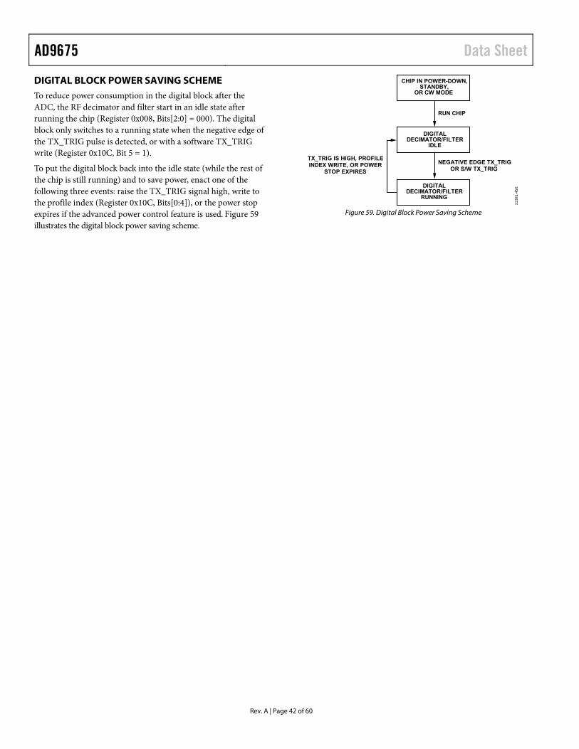
AD9675 Data Sheet
Rev. A | Page 42 of 60
DIGITAL BLOCK POWER SAVING SCHEME To reduce power consumption in the digital block after the ADC, the RF decimator and filter start in an idle state after running the chip (Register 0x008, Bits[2:0] = 000). The digital block only switches to a running state when the negative edge of the TX_TRIG pulse is detected, or with a software TX_TRIG write (Register 0x10C, Bit 5 = 1).
To put the digital block back into the idle state (while the rest of the chip is still running) and to save power, enact one of the following three events: raise the TX_TRIG signal high, write to the profile index (Register 0x10C, Bits[0:4]), or the power stop expires if the advanced power control feature is used. Figure 59 illustrates the digital block power saving scheme.
Figure 59. Digital Block Power Saving Scheme
CHIP IN POWER-DOWN,STANDBY,
OR CW MODE
DIGITALDECIMATOR/FILTER
IDLE
DIGITALDECIMATOR/FILTER
RUNNING
RUN CHIP
NEGATIVE EDGE TX_TRIGOR S/W TX_TRIG
TX_TRIG IS HIGH, PROFILEINDEX WRITE, OR POWER
STOP EXPIRES
1138
1-45
0

Data Sheet AD9675
Rev. A | Page 43 of 60
SERIAL PORT INTERFACE (SPI) The AD9675 SPI allows the user to configure the signal chain for specific functions or operations through the structured register space provided inside the chip. The SPI offers the user added flexibility and customization, depending on the application. Addresses are accessed via the serial port and can be written to or read from via the port. Memory is organized into bytes that can be further divided into fields, as documented in the Memory Map section. For detailed operational information, see the AN-877 Application Note, Interfacing to High Speed ADCs via SPI.
Three pins define the serial port interface: SCLK, SDIO, and CSB (see Table 28). The SCLK (serial clock) pin is used to synchronize the read and write data presented to the device. The SDIO (serial data input/output) pin is a dual-purpose pin that allows data to be sent to and read from the internal memory map registers of the device. The CSB (chip select bar) pin is an active low control that enables or disables the read and write cycles.
Table 28. Serial Port Pins Pin Function SCLK Serial clock. Serial shift clock input. SCLK
synchronizes serial interface reads and writes. SDIO Serial data input/output. Dual-purpose pin that
typically serves as an input or an output, depending on the instruction sent and the relative position in the timing frame.
CSB Chip select bar (active low). This control gates the read and write cycles.
The falling edge of CSB, in conjunction with the rising edge of SCLK, determines the start of the framing sequence. During the instruction phase, a 16-bit instruction is transmitted, followed by one or more data bytes, which is determined by Bit Field W0 and Bit Field W1. An example of the serial timing and its definitions are shown in Figure 61 and Table 29.
During normal operation, CSB signals to the device that SPI commands are to be received and processed. When CSB is brought low, the device processes SCLK and SDIO to execute instructions. Normally, CSB remains low until the communication cycle is complete. However, if connected to a slow device, CSB can be brought high between bytes, allowing older microcontrollers enough time to transfer data into shift registers. CSB can be stalled when transferring one, two, or three bytes of data. When W0 and W1 are set to 11, the device enters streaming mode and continues to process data, either reading or writing, until CSB is taken high to end the communication cycle. This mode allows complete memory transfers without the need for additional instructions. Regardless of the mode, if CSB is taken high in the middle of a byte transfer, the SPI state machine is reset, and the device waits for a new instruction.
The SPI port can be configured to operate in different manners. CSB can also be tied low to enable 2-wire mode. When CSB is tied low, SCLK and SDIO are the only pins required for
communication. Although the device is synchronized during power-up, exercise caution when using 2-wire mode to ensure that the serial port remains synchronized with the CSB line. When operating in 2-wire mode, use a 1-, 2-, or 3-byte transfer exclusively. Without an active CSB line, streaming mode can be entered but not exited.
In addition to word length, the instruction phase determines whether the serial frame is a read or write operation, allowing the serial port to be used both to program the chip and to read the contents of the on-chip memory. If the instruction is a read-back operation, performing a readback causes the serial data input/output (SDIO) pin to change direction from an input to an output at the appropriate point in the serial frame.
The user can send data in MSB first mode or LSB first mode. MSB first mode is the default at power-up and is changed by adjusting the configuration register (Address 0x000). For more information about this and other features, see the AN-877 Application Note, Interfacing to High Speed ADCs via SPI.
HARDWARE INTERFACE The pins described in Table 28 constitute the physical interface between the programming device and the serial port of the AD9675. The SCLK and CSB pins function as inputs when using the SPI. The SDIO pin is bidirectional, functioning as an input during write phases and as an output during readback.
If multiple SDIO pins share a common connection, ensure that proper VOH levels are met. Figure 60 shows the number of SDIO pins that can be connected together and the resulting VOH level, assuming the same load for each AD9675.
Figure 60. SDIO Pin Loading
This interface is flexible enough to be controlled either by serial programmable read-only memories (PROMs) or by PIC microcontrollers, which provide the user with an alternative to a full SPI controller for programming the device (see the AN-812 Application Note, Microcontroller-Based Serial Port Interface (SPI®) Boot Circuit).
NUMBER OF SDIO PINS CONNECTED TOGETHER
VO
H(V
)
1.715
1.720
1.725
1.730
1.735
1.740
1.745
1.750
1.755
1.760
1.765
1.770
1.775
1.780
1.785
1.790
1.795
1.800
0 302010 40 50 60 70 80 90 100
1138
1-05
6

AD9675 Data Sheet
Rev. A | Page 44 of 60
Figure 61. Serial Timing Details
Table 29. Serial Timing Definitions Parameter Timing (ns min) Description tDS 12.5 Setup time between the data and the rising edge of SCLK tDH 5 Hold time between the data and the rising edge of SCLK tCLK 40 Period of the clock tS 5 Setup time between CSB and SCLK tH 2 Hold time between CSB and SCLK tHIGH 16 Minimum period that SCLK must be in a logic high state tLOW 16 Minimum period that SCLK must be in a logic low state tEN_SDIO 15 Minimum time for the SDIO pin to switch from an input to an output relative to the SCLK falling
edge (not shown in Figure 61) tDIS_SDIO 15 Minimum time for the SDIO pin to switch from an output to an input relative to the SCLK rising
edge (not shown in Figure 61)
DON’TCARE
DON’TCARE
DON’TCARE
DON’TCARESDIO
SCLK
CSB
tS tDH
tHIGH tCLK
tLOW
tDS tH
R/W W1 W0 A12 A11 A10 A9 A8 A7 D5 D4 D3 D2 D1 D0
1138
1-05
7

Data Sheet AD9675
Rev. A | Page 45 of 60
MEMORY MAP READING THE MEMORY MAP TABLE Each row in the memory map register table has eight bit locations. The memory map is roughly divided into two sections: the chip configuration register map (Address 0x000 to Address 0x19E) and the profile register map (Address 0xF00 to Address 0xFFF). Registers that are designated as local registers use the device index in Address 0x004 and Address 0x005 to determine to which channels of a device the command is applied. Registers that are designated as chip registers use the chip address mode in Address 0x115 to determine whether the device is to be updated by writing to the chip register.
The first column of the memory map indicates the register address, and the default value is shown in the second rightmost column. The Bit 7 (MSB) column is the start of the default hexadecimal value given. For example, Address 0x011, the LNA and VGA gain adjustment register, has a default value of 0x06, meaning that Bit 7 = 0, Bit 6 = 0, Bit 5 = 0, Bit 4 = 0, Bit 3 = 0, Bit 2 = 1, Bit 1 = 1, and Bit 0 = 0, or 0000 0110 in binary. This setting is the default for GAIN± pins enabled, PGA gain = 24 dB, and LNA gain = 21.6 dB.
For more information about the SPI memory map and other functions, see the AN-877 Application Note, Interfacing to High Speed ADCs via SPI.
Reserved Locations
Do not write to undefined memory locations except when writing the default values suggested in this data sheet. Addresses that have values marked as 0 must be considered reserved and have a 0 written into their registers during power-up.
Default Values
After a reset, critical registers are automatically loaded with default values. These values are indicated in Table 31, where an X refers to an undefined feature (don’t care).
Logic Levels
An explanation of various registers follows: “bit is set” is synonymous with “bit is set to Logic 1” or “writing Logic 1 for the bit.” Similarly, “bit is cleared” is synonymous with “bit is set to Logic 0” or “writing Logic 0 for the bit.”
RECOMMENDED START-UP SEQUENCE To save system power during programming, the AD9675 powers up in power-down mode. To start the device up and initialize the data interface, the SPI commands listed in Table 30 are recommended. At a minimum, write the profile memory for an index of 0 (Address 0xF00 to Address 0xF07; see Table 27). If additional profiles and coefficient memory are required, write these profiles and coefficient memory blocks after Profile File Memory 0.

AD9675 Data Sheet
Rev. A | Page 46 of 60
Table 30. AD9675 SPI Write Start-Up Sequence Example Address Value Description 0x000 0x3C Initiate SPI reset 0x002 0x0X (default) Set speed mode to 40 MSPS 0x0FF 0x01 Enable speed mode change 0x004 0x0F Set local registers to all channels 0x005 0x3F Set local registers to all channels 0x113 0x00 Bypass RF decimator, enable high-pass filter 0x011 0x06 (default) Set LNA gain= 21.6 dB, GAIN± pins enabled, and PGA gain = 24 dB 0xF00 0xFF Continuous run mode enable; do not power down channels (POWER_STOP LSB) 0xF01 0x7F Continuous run mode enable; do not power down channels (POWER_STOP MSB) 0xF02 0x00 Power up all channels 0 clock cycles after TX_TRIG± signal assertion (POWER_START LSB) 0xF03 0x80 Digital high-pass bypassed (POWER_START MSB) 0x10C1 0x00 (default) Set index profile (required after profile memory writes) 0x014 0x00 Set output data format 0x008 0x00 Chip run (TGC mode)2 0x021 0x12 16-bit, four-lane mode 0x199 0x80 Enables automatic serializer/deserializer (SERDES) sample clock counter 0x142 0x04 ILAS enabled 0x188 0x01 Enable start code identifier 0x18B 0x27 Set start code MSB 0x18C 0x72 Set start code LSB 0x150 0x03 JESD204B scrambler disabled and four-lane configuration (L = 4) 0x182 0x82 Automatically configures PLL 0x181 0x02 PLL N-divider = ÷20 0x186 0xAA Disable continuous data resync (continuous data resync is not recommended during real-time
scanning; one time data resync is sufficient) 0x10C3 0x20 Set SPI TX_TRIG± and index profile 0x00F 0x18 Set low-pass filter cutoff frequency, bandwidth mode 0x02B 0x40 Set analog LPF and HPF to defaults, tune filters4 1 Setting the profile index requires an additional SPI write in SPI MSB mode before the chip is run to complete the current profile buffer update. 2 Running the chip from full power-down mode requires 375 μs wake up time as listed in Table 3. 3 Soft TX_TRIG switches the RF decimator and filter to a running state. The soft TX_TRIG may not be needed if a hardware TX_TRIG signal is used to run the digital block. 4 Tuning the filters requires 512 ADC clock cycles.

Data Sheet AD9675
Rev. A | Page 47 of 60
MEMORY MAP REGISTER TABLE
Table 31. AD9675 Memory Map Registers Addr. (Hex)
Register Name
Bit 7 (MSB) Bit 6 Bit 5 Bit 4 Bit 3 Bit 2 Bit 1
Bit 0 (LSB)
Default Value Comments
Chip Configuration Registers
0x000 CHIP_ PORT_ CONFIG
0 LSB first 0 = off (default) 1 = on
SPI reset 0 = off (default) 1 = on
1 1 SPI reset 0 = off (default) 1 = on
LSB first 0 = off (default) 1 = on
0 0x18 Nibbles mirrored so that LSB or MSB first mode is set correctly regardless of shift mode. SPI reset reverts all registers (including the JESD ones), except Reg. 0x000 to their default values and 0x000[2, 5] bits are automatically cleared.
0x001 CHIP_ ID
Chip ID Bits[7:0] AD9675 = 0xA9 (default)
0xA9 Default is unique chip ID, different for each device; read only register
0x002 CHIP_ GRADE
X X Speed mode (identify device
variants of chip ID) 00: Mode I
(40 MSPS) (default) 01: Mode II (65 MSPS) 10: Mode III (80 MSPS)
11: Mode III (125 MSPS)
X X X X 0x0X Speed mode used to diff-erentiate ADC speed power modes (must update Reg. 0x0FF to initiate mode setting)
Device Index and Update Registers
0x004 DEVICE_ INDEX_2
X X X X Data Channel H 0 = off 1 = on (default)
Data Channel G 0 = off 1 = on (default)
Data Channel F 0 = off 1 = on (default)
Data Channel E 0 = off 1 = on (default)
0x0F Bits are set to determine which on-chip device receives the next write command.
0x005 DEVICE_ INDEX_1
X X 1 1 Data Channel D 0 = off 1 = on (default)
Data Channel C0 = off 1 = on (default)
Data Channel B 0 = off 1 = on (default)
Data Channel A 0 = off 1 = on (default)
0x3F Bits are set to determine which on-chip device receives the next write command.

AD9675 Data Sheet
Rev. A | Page 48 of 60
Addr. (Hex)
Register Name
Bit 7 (MSB) Bit 6 Bit 5 Bit 4 Bit 3 Bit 2 Bit 1
Bit 0 (LSB)
Default Value Comments
0x0FF DEVICE_ UPDATE
X X X X X X X Update speed mode 0 = off (default) 1 = on
0x00 A write to Reg 0xFF (value does not matter) resets all default reg-ister values (analog and ADC registers only, not JESD registers, Reg 0x00 or Reg 0x02[4:5]) if Reg 0x02 was prev-iously written since the last reset/load of defaults.
Program Function Registers
0x008 GLOBAL_ MODES
X LNA input impe-dance 0 = 6 kΩ (default) 1= 3 kΩ
X 0 0 Internal power-down mode 000 = chip run (TGC mode)
001 = full power-down (default) 010 = standby
011 = reset all JESD registers 100 = CW mode (TGC power-down)
0x01 Determines generic modes of chip operation (global)
0x009 GLOBAL_ CLOCK
X X X X X X X DCS 0 = off 1 = on (default)
0x01 Turns the internal duty cycle stabilizer (DCS) on and off (global)
0x00A PLL_ STATUS
PLL lock status 0 = not locked 1 = locked
X X X X X X JESD204B link ready status 0 = link not ready (default) 1 = link ready, PLL locked
0x00 Monitor PLL lock and link ready status (read only, global)
0x00D TEST_IO User test mode 0 = con-tinuous, repeat user patterns (1, 2, 3, 4, 1, 2, 3, 4, …) (default) 1 = single clock cycle user patterns, then zeros (1, 2, 3, 4, 0, 0, …)
X Reset PN long gen 0 = on, PN long running (default) 1 = off, PN long held in reset
Reset PN short gen 0 = on, PN short running (default) 1 = off, PN short held in reset
Output test mode 0000 = off (default)
0001 = midscale short 0010 = +FS short 0011 = −FS short
0100 = checkerboard output 0101 = PN sequence long 0110 = PN sequence short
0111 = one-/zero-word toggle 1000 = user input
1001 to 1110 = reserved 1111 = ramp output
0x00 When this register is set, the test data is placed on the output pins in place of normal data (local)
0x00E GPO X X X X General-purpose digital outputs 0x00 Values placed on GPO0 to GPO3 pins (global)

Data Sheet AD9675
Rev. A | Page 49 of 60
Addr. (Hex)
Register Name
Bit 7 (MSB) Bit 6 Bit 5 Bit 4 Bit 3 Bit 2 Bit 1
Bit 0 (LSB)
Default Value Comments
0x00F FLEX_ CHANNEL_ INPUT
Filter cutoff frequency control 0 0000 = 1.45 × (1/3) × fSAMPLE 0 0001 = 1.25 × (1/3) × fSAMPLE 0 0010 = 1.13 × (1/3) × fSAMPLE
0 0011 = 1.0 × (1/3) × fSAMPLE (default) 0 0100 = 0.9 × (1/3) × fSAMPLE 0 0101 = 0.8 × (1/3) × fSAMPLE
0 0110 = 0.75 × (1/3) × fSAMPLE 0 0111 = N/A
0 1000 = 1.45 × (1/4.5) × fSAMPLE 0 1001 = 1.25 × (1/4.5) × fSAMPLE 0 1010 = 1.13 × (1/4.5) × fSAMPLE 0 1011 = 1.0 × (1/4.5) × fSAMPLE 0 1100 = 0.9 × (1/4.5) × fSAMPLE 0 1101 = 0.8 × (1/4.5) × fSAMPLE
0 1110 = 0.75 × (1/4.5) × fSAMPLE 0 1111 = N/A
1 0000 = 1.45 × (1/6) × fSAMPLE 1 0001 = 1.25 × (1/6) × fSAMPLE 1 0010 = 1.13 × (1/6) × fSAMPLE 1 0011 = 1.0 × (1/6) × fSAMPLE 1 0100 = 0.9 × (1/6) × fSAMPLE 1 0101 = 0.8 × (1/6) × fSAMPLE
1 0110 = 0.75 × (1/6) × fSAMPLE 1 0111 = N/A
BW mode 0 = low (default, 8 MHz to 18 MHz) 1 = high (13.5 MHz to 30 MHz)
X X 0x18 Antialiasing filter cutoff (global)
0x010 FLEX_ OFFSET
X X 1 0 0 0 0 0 0x20 Reserved
0x011 FLEX_ GAIN
Digital VGA gain control 0000 = GAIN± pins enabled (default)
0001 = 0.0 dB (max gain, GAIN± pins disabled) 0010 = −3.5 dB 0011 = −7.0 dB
… 1110 = −45 dB
1111 = reserved (do not use)
PGA gain 00 = 21 dB
01 = 24 dB (default) 10 = 27 dB 11 = 30 dB
LNA gain 00 = 15.6 dB 01 = 17.9 dB 10 = 21.6 dB
(default) 11 = reserved
0x06 LNA and PGA gain adjustment (global)
0x012 BIAS_ CURRENT
X X X X 1 PGA bias 0 =100% (default) 1 = 60%
LNA bias 00 = high
01 = midhigh (default) 10 = midlow
11 = low
0x09 LNA bias current adjustment (global)
0x013 RESERVED_13
0 0 0 0 0 0 0 0 0x00 Reserved
0x014 OUTPUT_ MODE
X X X Output data enable 0 = enable (default) 1 = disable
X Output data invert 0 = disable (default) 1 = enable
Output data format 00 = offset binary
01 = twos complement (default)
10 = gray code 11 = reserved
0x01 Data output modes (local)
0x015 OUTPUT_ ADJUST
X CML output drive level adjustment 000 = reserved 001 = reserved 010 = 368 mV
011 = reserved 100 = 293 mV 101 = 286 mV
110 = 262 mV (default) 111 = 238 mV
X X Output pre-emphasis 0 = off (default) 1 = on
1 0x61 Data output levels (global)

AD9675 Data Sheet
Rev. A | Page 50 of 60
Addr. (Hex)
Register Name
Bit 7 (MSB) Bit 6 Bit 5 Bit 4 Bit 3 Bit 2 Bit 1
Bit 0 (LSB)
Default Value Comments
0x016 RESERVED_16
X X X X X X X X 0x00
0x017 RESERVED_17
X X X X X X X X 0x00
0x018 FLEX_ VREF
X X X X X 1 0 0 0x04 Reserved (global)
0x019 USER_ PATT1_ LSB
B7 B6 B5 B4 B3 B2 B1 B0 0x00 User-Defined Pattern 1, LSB (global)
0x01A USER_ PATT1_ MSB
B15 B14 B13 B12 B11 B10 B9 B8 0x00 User-Defined Pattern 1, MSB (global)
0x01B USER_ PATT2_ LSB
B7 B6 B5 B4 B3 B2 B1 B0 0x00 User-Defined Pattern 2, LSB (global)
0x01C USER_ PATT2_ MSB
B15 B14 B13 B12 B11 B10 B9 B8 0x00 User-Defined Pattern 2, MSB (global)
0x01D USER_ PATT3_ LSB
B7 B6 B5 B4 B3 B2 B1 B0 0x00 User-Defined Pattern 3, LSB (global)
0x01E USER_ PATT3_ MSB
B15 B14 B13 B12 B11 B10 B9 B8 0x00 User-Defined Pattern 3, MSB (global)
0x01F USER_ PATT4_ LSB
B7 B6 B5 B4 B3 B2 B1 B0 0x00 User-Defined Pattern 4, LSB (global)
0x020 USER_ PATT4_ MSB
B15 B14 B13 B12 B11 B10 B9 B8 0x00 User-Defined Pattern 4, MSB (global)
0x021 FLEX_ SERIAL_ CTRL
0 X Lane mode 00 = reserved (default) 01 = 2 channels/lane
(4 lanes) 10 = 4 channels/lane
(2 lanes) 11 = 8 channels/lane
(1 lane)
Lane low rate: 0 = normal (default) 1 = low output rate (<1 Gbps)
X Output word length 00 = 12 bits (default)
01 = 14 bits 10 = 16 bits
11 = reserved
0x00 Lane setting control (global)
0x022 SERIAL_ CH_STAT
X X X X X X X Channel power-down 1 = on 0 = off (default)
0x00 Used to power down individual channels (local)
0x02B FLEX_ FILTER
X Enable automatic low-pass tuning 1 = on (self clearing)
X X Bypass analog HPF 0 = off (default) 1 = on
X Analog high-pass filter cutoff
00 = fLP/12.00 (default) 01 = fLP/9.00 10 = fLP/6.00 11 = fLP/3.00
0x00 Filter cutoff (global) (fLP = low-pass filter cutoff frequency)
0x02C LNA_ TERM
X X X X X X LO-x, LOSW-x connection
00 = RFB1 + 50 Ω (default) 01 = (RFB1||RFB2) + 50 Ω
10 = RFB2 + 50 Ω 11 = ∞
0x00 LNA active termination/input impedance (global)

Data Sheet AD9675
Rev. A | Page 51 of 60
Addr. (Hex)
Register Name
Bit 7 (MSB) Bit 6 Bit 5 Bit 4 Bit 3 Bit 2 Bit 1
Bit 0 (LSB)
Default Value Comments
0x02D CW_ ENABLE_ PHASE
X X X CW Doppler channel enable 1 = on 0 = off
I/Q demodulator phase 0000 = 0° (default)
0001 = 22.5° (not valid for 4LO mode) 0010 = 45°
0011 = 67.5° (not valid for 4LO mode) 0100 = 90°
0101 = 112.5° (not valid for 4LO mode) 0110 = 135°
0111 = 157.5° (not valid for 4LO mode) 1000 = 180°
1001 = 202.5° (not valid for 4LO mode) 1010 = 225°
1011 = 247.5° (not valid for 4LO mode) 1100 = 270°
1101 = 292.5° (not valid for 4LO mode) 1110 = 315°
1111 = 337.5° (not valid for 4LO mode)
0x00 Phase of demodu-lators (local)
0x02E CW_LO_ MODE
Enable JESD during CW 0: JESD link disabled during CW (default) 1: JESD link enabled during CW (switching activity can de-grade CW perfor-mance)
RESET± with MLO± clock edge 0 = synchro-nous (default) 1 = asynchro-nous
Synchro-nous RESET± sampling MLO± clock edge 0 = falling (default) 1 = rising
RESET± polarity 0 = active high (default) 1 = active low
MLO± and RESET± buffer enable (in all modes except CW mode) 0 = power-down (default) 1 = enable
LO mode 00X = 4LO, 3rd to 5th odd harmonic
rejection (default) 010 = 8LO, 3rd to 5th odd harmonic
rejection 011 = 8LO, 3rd to 13th odd harmonic
rejection 100 = 16LO, 3rd to 5th odd harmonic
rejection 101 = 16LO, 3rd to 13th odd harmonic
rejection 11X = reserved
0x00 CW mode functions (global)
0x02F CW_ OUTPUT
CW output dc bias voltage 0 = bypass 1 = enable (default)
0 0 0 0 0 0 0 0x80 Global
0x102 RESERVED_102
0 0 0 0 0 0 0 0 0X00 Reserved
0x103 RESERVED_103
0 0 0 0 0 0 0 0 0X00 Reserved
0x104 RESERVED_104
0 0 1 1 1 1 1 1 0x3F Reserved
0x105 RESERVED_105
0 0 0 0 0 0 0 0 0x00 Reserved
0x106 RESERVED_106
0 0 0 0 0 0 0 0 0x00 Reserved
0x107 RESERVED_107
0 0 0 0 0 0 X X Read only
Reserved
0x108 RESERVED_108
0 0 0 0 0 0 0 0 0x00 Reserved

AD9675 Data Sheet
Rev. A | Page 52 of 60
Addr. (Hex)
Register Name
Bit 7 (MSB) Bit 6 Bit 5 Bit 4 Bit 3 Bit 2 Bit 1
Bit 0 (LSB)
Default Value Comments
0x109 VGA_TEST X X X VGA/ AAF test enable 0 = off (default) 1 = on
X VGA/AAF output test mode 000 = Channel A (default)
001 = Channel B 010 = Channel C 011 = Channel D 100 = Channel E 101 = Channel F 110 = Channel G 111 = Channel H
0x00 VGA/AAF test mode enables AAF output to GPO2/ GPO3 pins (global)
0x10C PROFILE_ INDEX
X X Manual TX_TRIG signal 0 = off, use pin (default) 1 = on, auto-generate TX_TRIG (self-clears)
Profile index[4:0] 0x00 Index for profile memory selects active profile (global)
0x10D RESERVED_10D
1 1 1 1 1 1 1 1 0xFF Reserved
0x10E RESERVED_10E
1 1 1 1 1 1 1 1 0xFF Reserved
0x10F DIG_ OFFSET_ CAL
0 0 0 0 Digital offset calibration status 0 = not complete (default) 1 = complete
Digital offset calibration 000 = disable correction, reset correction
value (default) 001 = average 210 samples 010 = average 211 samples
… 111 = average 216 samples
0x00 Control digital offset calibration enable and number of samples used (global)
0x110 DIG_ OFFSET_ CORR1
D7 D6 D5 D4 D3 D2 D1 D0 0x00 Offset correction LSB (local)
0x111 DIG_ OFFSET_ CORR2
D15 D14 D13 D12 D11 D10 D9 D8 0x00 Offset correction MSB (local)
Digital offset calibration (read back if autocalibration enabled with Register 0x10F. Otherwise, force correction value.)
Offset correction = [D15:D0] × full scale/216 0111 1111 1111 1111 (215 − 1) = +1/2 full scale − 1/216 full scale 0111 1111 1111 1110 (215 – 2) = +1/2 full scale − 2/216 full scale
… 0000 0000 0000 0001 (+1) = +1/216 full scale
0000 0000 0000 0000 = no correction (default) 1111 1111 1111 1111 (−1) = −1/216 full scale
… 1000 0000 0000 0000 (−215) = −1/2 full scale
0x112 POWER_ MASK_ CONFIG
X X X Power-up setup time (POWER_SETUP) 0 0000 = 0
0 0001 = 1 × 40/fSAMPLE
0 0010 = 2 × 40/fSAMPLE (default) 0 0011 = 3 × 40/fSAMPLE
… 1 1111 = 31 × 40/fSAMPLE
0x02 POWER_ SETUP time is used to set the power-up time (global)
0x113 DIG_ CONFIG
X X Digital high-pass filter 0 = enable (default) 1 = bypass
X Decimator and filter enable
00 = RF 2× decimator bypassed (default)
01 = RF 2× decimator enabled and low bandwidth filter
1X = RF 2× decimator enabled and high bandwidth filter
X X 0x00 Enable stages of the digital processing (global)

Data Sheet AD9675
Rev. A | Page 53 of 60
Addr. (Hex)
Register Name
Bit 7 (MSB) Bit 6 Bit 5 Bit 4 Bit 3 Bit 2 Bit 1
Bit 0 (LSB)
Default Value Comments
0x115 CHIP_ ADDR_EN
X X Chip address mode 0 = disable (default) 1 = enable
Chip address qualifier 0 0000 (default)
(If read, returns the state of ADDR0 to ADRR4 pins)
0x00 Chip address mode en-ables the addressing of devices if the value of chip address qualifier equals the state on the address pins, ADDRx (global)
0x116 ANALOG_ TEST_ TONE
X X X X Analog test tone amplitude
See Table 23 to Table 25
Analog test tone frequency
00 = fSAMPLE/4 (default) 01 = fSAMPLE/8
10 = fSAMPLE/16 11 = fSAMPLE/32
0x00 Analog test tone amplitude and frequency (global)
0x117 DIG_ SINE_ TEST_ FREQ
X X X Digital test tone frequency 0 0000 = 1 × fSAMPLE/64 0 0001 = 2 × fSAMPLE/64
… 1 1111 = 32 × fSAMPLE/64
0x00 Digital sine test tone frequency (global)
0x118 DIG_ SINE_ TEST_ AMP
X X X X Digital test tone amplitude 0000 = AFULL-SCALE (default)
0001 = AFULL-SCALE/2 0010 = AFULL-SCALE/22
… 1111 = AFULL-SCALE/215
0x00 Digital sine test tone amplitude (global)
0x119 DIG_ SINE_ TEST_ OFFSET
Offset multiplier (a) 0 1111 = 15 0 1110 = 14
… 0 0000 = 0 (default)
1 1111 = −1 …
1 0000 = −16
Offset exponent (b) 000 = 0 (default)
001 = 1 …
111 = 7
0x00 Digital sine test tone offset (global)
Offset = AFULL-SCALE × a × 2−(13 − b)
Offset range is ~0.5 dB Maximum positive offset = 15 × 2−(13 − 7) = 0.25 × AFULL-SCALE
Maximum negative offset = −16 × 2−(13 − 7) ≈ −0.25 × AFULL-SCALE 0x11A TEST_
MODE_ CHENABLE
Ch H enable 0 = off (default) 1 = on
Ch G enable 0 = off (default) 1 = on
Ch F enable 0 = off (default) 1 = on
Ch E enable 0 = off (default) 1 = on
Ch D enable 0 = off (default) 1 = on
Ch C enable 0 = off (default) 1 = on
Ch B enable 0 = off (default) 1 = on
Ch A enable 0 = off (default) 1 = on
0x00 Enable channels for test mode (global)
0x11B TEST_ MODE_ CONFIG
X X X X X Data path test mode selection 000 = disable test modes (default)
001 = enable digital sine test mode 010 = reserved
011 = enable channel ID test mode (16-bit data = digital ramp (7 bits) +
reserved bit (0) + Channel ID (3 bits) + Chip Address (5 bits)
100 = enable analog test tone 101 = reserved
… 111 = reserved
0x00 Enable digital test modes (local)
0x11C RESERVED_11C
0 0 0 0 0 0 0 0 0x00 Reserved
0x11D RESERVED_11D
0 0 0 0 0 0 0 0 0x00 Reserved

AD9675 Data Sheet
Rev. A | Page 54 of 60
Addr. (Hex)
Register Name
Bit 7 (MSB) Bit 6 Bit 5 Bit 4 Bit 3 Bit 2 Bit 1
Bit 0 (LSB)
Default Value Comments
0x11E RESERVED_11E
0 0 0 0 0 0 0 0 0x00 Reserved
0x11F RESERVED_11F
0 0 0 0 0 0 0 0 0x00 Reserved
0x120 CW_ TEST_ TONE
0 CW I/Q output swap 0 = disable (default) 1 = enable
LNA offset cancella-tion 0 = enable (default) 1 = disable
LNA offset cancellation transconductance
00 = 0.5 mS (default) 01 = 1.0 mS 10 = 1.5 mS 11 = 2.0 mS
CW analog test tone override for
Address 0x116, Bits [1:0] 00 = disable override
(default) 01 = set analog test
tone frequency to fLO
1X = set analog test tone frequency to dc
0 0x00 Sets the frequency of the analog test tone to fLO in CW Doppler mode; enables I/Q output swap; LNA offset cancellation control (global)
0x142 JTX_ LINK_ CTRL1
JESD204B power during standby 0 = remain powered up (default) 1 = power down
JESD204B tail bit value 0 = zeros (default) 1 = PN sequence
JESD204B test mode enable 0 = disable (default) 1 = enable
JESD204B lane sync enable 0 = disable (default) 1 = enable
JESD204B ILAS enable 00 = disable (default)
01 = enable 10 = always on, test
mode 11 = reserved
JESD204B serial frame alignment character insertion (FACI) disable 0: FACI enabled 1: FACI disabled
Power down JESD204B link 0 = link enabled (default) 1 = link powered down
0x00 JESD204B configuration (global)
0x143 JTX_ LINK_ CTRL2
SYNCINB signal polarity 0 = not inverted (default) 1 = inverted
0 0 8-bit/ 10-bit encoder 0 = enable (default) 1 = bypass (test mode only)
10-bit transmit bit invert 0 = not inverted (default) 1 = inverted SERD-OUTx±
10-bit transmit bit mirror 0 = not mirrored (default) 1 = mirrored
0x00 JESD204B configuration (global)
0x144 JTX_ LINK_ CTRL3
Checksum enable 0 = enable (default) 1 = disable
Checksum algorithm 0 = add parameter (default) 1 = add packed octets
JESD204B test pattern input selection
00 = reserved (default) 01 = 10-bit test data injected at output of 8-bit/10-bitencoder 10 = 8-bit test data injected at input of
scrambler 11 = reserved
JESD204B test mode selection 0000 = off (default)
0001 = alternating checkerboard 0010 = 1-/0-word toggle 0011 = PN sequence long 0100 = PN sequence short
0101 = continuous/repeat user test pattern 0110 = single user test pattern
0111 = ramp output 1000 = RPAT sequence
1001 = reserved …
1111 = reserved
0x00 JESD204B test mode and checksum controls (global)
0x145 JTX_ LINK_ CTRL4
Initial lane alignment sequence repeat count 0000 0000 = 4 × K + 1 (default)
0000 0001 = 4 × K + 2 …
1111 1111 = 4 × K + 128
0x00 JESD204B ILAS repeat count (global)
0x146 JTX_DID_ CFG
JESD204B serial device identification (DID) number 0x00 Global
0x147 JTX_BID_ CFG
X X X X JESD204B serial bank identification (BID) number (extension to DID)
0x00 Global
0x148 JTX_LID0_ CFG
X X X Serial lane identification (LID) number for Lane 1 0x00 Global
0x149 JTX_LID1_ CFG
X X X Serial lane identification (LID) number for Lane 2 0x01 Global

Data Sheet AD9675
Rev. A | Page 55 of 60
Addr. (Hex)
Register Name
Bit 7 (MSB) Bit 6 Bit 5 Bit 4 Bit 3 Bit 2 Bit 1
Bit 0 (LSB)
Default Value Comments
0x14A JTX_LID2_ CFG
X X X Serial lane identification (LID) number for Lane 3 0x02 Global
0x14B JTX_LID3_ CFG
X X X Serial lane identification (LID) number for Lane 4 0x03 Global
0x14C RESERVED_14C
0 0 0 0 0 0 0 0 0x00 Reserved
0x14D RESERVED_14D
0 0 0 0 0 0 0 0 0x00 Reserved
0x14E RESERVED_14E
0 0 0 0 0 0 0 0 0x00 Reserved
0x14F RESERVED_14F
0 0 0 0 0 0 0 0 0x00 Reserved
0x150 JTX_SCR_ L_CFG
JESD204B serial scrambler mode 0 = disabled 1 = enabled (default)
X X X X X Lanes per link 00 = one lane (L = 1) 01 = two lanes (L = 2)
10 = reserved 11 = four lanes (L = 4)
(default)
0x83 JESD204B scrambler and lane configuration (global)
0x151 JTX_F_ CFG
X X X Number of octets per frame (F) F = (M × 2)/(L)
0 0000 = reserved …
0 0011 = 4 octets ( M = 8, L = 4, default) 0 0100 = reserved
… 0 0111 = 8 octets (M = 8, L = 2) or (M = 16, L = 4)
0 1000 = reserved …
0 1111 = 16 octets (M = 8, L = 1) or (M = 16, L = 2) 1 0000 = reserved
… 1 1111 = 32 octets (M = 16, L = 1)
0x03 JESD204B number of octets per frame (read only, global)
0x152 JTX_K_ CFG
X X X Number of frames per multiframe (K) 0 0000 = 1 0 0001 = 2
… 1 1111 = 32
0x0F JESD204B frames per multiframe (global)
0x153 JTX_M_ CFG
X X X X Number of converters per link 0000 = reserved
… 0111 = 8 channels, real data (M = 8)
1000 = reserved …
1111 = 8 channels, quadrature data (M = 16)
0x07 JESD204B number of converter per link (read only, global)
0x154 JTX_CS_ N_CFG
X Control bits per sample 0 = none (CS = 0, default, read only)
X 0 Output resolution (N) 0000 = reserved
… 1011 = 12 bits
1100 = reserved 1101 = 14 bits
1110 = reserved 1111 = 16 bits (default)
0x0F JESD204B serializer number of bits per channel (global)
0x155 JTX_SCV_ NP_CFG
0 0 0 0 Bits per output sample (N') 0000 = reserved
… 1110 = reserved
1111 = 16 (default)
0x0F JESD204B number of bits per samples (global, read only)

AD9675 Data Sheet
Rev. A | Page 56 of 60
Addr. (Hex)
Register Name
Bit 7 (MSB) Bit 6 Bit 5 Bit 4 Bit 3 Bit 2 Bit 1
Bit 0 (LSB)
Default Value Comments
0x156 JTX_JV_ S_CFG
X X Number of clocks SYNCINB signal must be low for synchro-nization to begin 0 = 2 frame clock cycles 1 = 4 frame clock cycles (default)
0 0 0 0 Samples per channel per frame (S) 0 = 1 sample (default, read only) 1 = 2 samples
0x20 Number of clocks SYNCINB signal must be low for synchro-nization to begin (global)
0x157 JTX_HD_ CF_CFG
0 0 0 Control words per frame clock per link 0 0000 = 0 (default) 0 0001 = reserved
… 1 1111 = reserved
0x00 JESD204B control words per frame (global, read only)
0x158 JTX_RES1_CFG
0 0 0 0 0 0 0 0 0x00 Reserved
0x159 JTX_RES2_CFG
0 0 0 0 0 0 0 0 0x00 Reserved
0x15A JTX_ CHKSUM0_CFG
Checksum value for Lane 1 (FCHK) 0x3C JESD204B checksum value Lane 1 (global, read only)
0x15B JTX_ CHKSUM1_CFG
Checksum value for Lane 2 (FCHK) 0x3D JESD204B checksum value Lane 2 (global, read only)
0x15C JTX_ CHKSUM2_CFG
Checksum value for Lane 3 (FCHK) 0x3E JESD204B checksum value Lane 3 (global, read only)
0x15D JTX_ CHKSUM3_CFG
Checksum value for Lane 4 (FCHK) 0x3F JESD204B checksum value Lane 4 (global, read only)
0x15E RESERVED_15E
0 1 1 0 1 1 0 0 0x3C Reserved
0x15F RESERVED_15F
0 1 1 0 1 1 0 0 0x3C Reserved
0x160 RESERVED_160
0 1 1 0 1 1 0 0 0x3C Reserved
0x161 RESERVED_161
0 1 1 0 1 1 0 0 0x3C Reserved
0x170 RESERVED_170
0 0 0 0 0 0 0 0 0x00 Reserved
0x171 RESERVED_171
1 1 1 1 1 1 1 1 0xFF Reserved
0x172 RESERVED_172
1 1 1 1 1 1 1 1 0xFF Reserved
0x173 RESERVED_173
0 0 0 0 0 0 0 0 0x00 Reserved
0x174 RESERVED_174
0 0 0 0 1 1 1 1 0x0F Reserved
0x180 JTX_CLK_ CNTL_1
1 0 0 0 0 1 1 1 0x87 Reserved

Data Sheet AD9675
Rev. A | Page 57 of 60
Addr. (Hex)
Register Name
Bit 7 (MSB) Bit 6 Bit 5 Bit 4 Bit 3 Bit 2 Bit 1
Bit 0 (LSB)
Default Value Comments
0x181 JTX_CLK_ CNTL_2
0 0 0 0 0 PLL N-divider setting (in powers of 2) 000 = divide by 1 (Z = ÷5, default)
001 = divide by 2 (Z = ÷10) 010 = divide by 4 (Z = ÷20) 011 = divide by 8 (Z = ÷40)
100 = divide by 16 (Z = ÷80) 101 = reserved 110 = reserved 111 = reserved
0x00 PLL N-divider setting (global)
0x182 PLL_ STARTUP
PLL auto-configure 0 = disable (default) 1 = enable
0 0 0 0 0 1 0 0x02 PLL control (global)
0x183 RESERVED_183
0 0 0 0 0 1 1 1 0x07 Reserved
0x184 RESERVED_184
0 0 0 0 0 0 0 0 0x00 Reserved
0x186 DATA_ VALID_ RESYNC
1 0 1 0 One time data resync with JESD clock after TX_TRIG 0 = disable resync 1 = enable resync (default)
Continu-ous data resync with JESD clock 0 = disable resync 1 = enable resync (default)
One time SYSREF resync with JESD clock after TX_TRIG 0 = disable resync 1 = enable resync (default)
Continuous SYSREF resync with JESD clock 0 = disable resync (default) 1 = enable resync
0xAE Data and SYSREF resync
0x188 START_ CODE_EN
0 0 0 0 0 0 0 Start code identifier 0 = disable 1 = enable (default)
0x01 Enable start code identifier (global)
0x189 RESERVED 0 0 0 0 0 0 0 0 0x00 Reserved
0x18A RESERVED 0 0 0 0 0 0 0 0 0x00 Reserved
0x18B START_ CODE_ MSB
0 0 1 0 0 1 1 1 0x27 Start code MSB (global)
0x18C START_ CODE_ LSB
0 1 1 1 0 0 1 0 0x72 Start code LSB (global)
0x190 FRAME_ SIZE_ MSB
X X X Automa-tically set frame size 0 = disable 1 = enable (default)
X X X X 0x10 Automati-cally set frame size (global)
0x191 RESERVED_191
0 0 0 0 0 0 0 0 0x00 Reserved
0x192 RESERVED_192
0 0 0 1 1 0 0 0 0x18 Reserved
0x193 RESERVED_193
0 0 0 0 0 0 0 0 0x00 Reserved
0x194 RESERVED_194
0 0 0 1 1 1 0 0 0x1C Reserved
0x195 RESERVED_195
0 0 0 0 0 0 0 0 0x00 Reserved
0x196 RESERVED_196
0 0 0 1 1 0 0 0 0x18 Reserved

AD9675 Data Sheet
Rev. A | Page 58 of 60
Addr. (Hex)
Register Name
Bit 7 (MSB) Bit 6 Bit 5 Bit 4 Bit 3 Bit 2 Bit 1
Bit 0 (LSB)
Default Value Comments
0x197 RESERVED_197
0 0 0 0 0 0 0 0 0x00 Reserved
0x198 RESERVED_198
0 0 0 0 0 0 0 0 0x00 Reserved
0x199 SAMPLE_ CLOCK_ COUNTER
SERDES clock counter 0 = disable (default) 1 = enable
0 0 0 0 0 0 0 0x00 Enables automatic SERDES sample clock counter
0x19A RESERVED_19A
0 0 0 0 0 0 0 0 0x00 Reserved
0x19B RESERVED_19B
0 1 1 1 0 0 0 0 0x70 Reserved
0x19C JTX_ FRAME_ SIZE
X X X Set frame size automa-tically 0 = disable 1 = enable (default)
X X 0 0 0x10 Automatic-ally set JESD204B frame size (global)
0x19D RESERVED_19D
0 0 0 0 0 0 0 0 0x00 Reserved
0x19E RESERVED_19E
0 0 0 1 0 0 0 0 0x10 Reserved
Profile Memory Registers
0xF00 to 0xFFF
Profile Memory
32 × 64 bits 0x00 Global

Data Sheet AD9675
Rev. A | Page 59 of 60
MEMORY MAP REGISTER DESCRIPTIONS For more information about the SPI memory map and other functions, see the AN-877 Application Note, Interfacing to High Speed ADCs via SPI.
Transfer (Register 0x0FF)
All registers except Register 0x002 are updated as soon as they are written. Writing to Register 0x0FF (the value written is don’t care) initializes and updates the speed mode (Address 0x002) and resets all other registers to their default values (analog and ADC registers only, and not JESD204B registers, Register 0x000, or Register 0x002). Set the speed mode in Register 0x002 and write to Register 0x0FF at the beginning of the setup of the SPI writes after the device is powered up to avoid rewriting other registers after Register 0x0FF is written.
Profile Index and Software TX_TRIG (Register 0x10C)
The vector profile is selected using the profile index in Register 0x10C, Bits[4:0]. The software TX_TRIG control in Bit 5 generates a TX_TRIG signal internal to the device. This signal is asynchronous to the ADC sample clock. Therefore, do not used this signal to align the data output or to initiate advanced power mode across multiple devices in the system. The external pin-driven TX_TRIG± control is recommended for systems that require synchronization of these features across multiple AD9675 devices.

AD9675 Data Sheet
Rev. A | Page 60 of 60
OUTLINE DIMENSIONS
Figure 62. 144-Ball Chip Scale Package, Ball Grid Array [CSP_BGA]
(BC-144-1) Dimensions shown in millimeters
ORDERING GUIDE Model1 Temperature Range Package Description Package Option AD9675KBCZ 0°C to 85°C 144-Ball Chip Scale Package, Ball Grid Array [CSP_BGA] BC-144-1 AD9671EBZ Evaluation Board 1 Z = RoHS Compliant Part.
*COMPLIANT WITH JEDEC STANDARDS MO-275-EEAB-1WITH EXCEPTION TO PACKAGE HEIGHT. 10
-21-
2010
-B
0.80
0.60REF
A
B
C
D
E
F
G
910 81112 7 56 4 23 1
BOTTOM VIEW
8.80BSC SQ
H
J
K
L
M
DETAIL A
TOP VIEW
DETAIL A
COPLANARITY0.20
0.500.450.40
*1.40 MAX
BALL DIAMETER
SEATINGPLANE
10.1010.00 SQ9.90A1 BALL
CORNER
A1 BALLCORNER
0.25 MIN
0.65 MIN
©2013–2016 Analog Devices, Inc. All rights reserved. Trademarks and registered trademarks are the property of their respective owners. D11381-0-1/16(A)