ocp accelerator module design specification · 5 ocp accelerator module design specification v1.0 2...
TRANSCRIPT

1 OCP Accelerator Module Design Specification v1.0
OCP Accelerator Module Design
Specification v1.0
Author:
Whitney Zhao, Hardware Engineer, Facebook
Tiffany Jin, Mechanical Engineer, Facebook
Cheng Chen, Thermal Engineer, Facebook
Siamak Tavallaei, Principal Architect, Microsoft
Zhenghui Wu, Staff System Engineer, Baidu

2 OCP Accelerator Module Design Specification v1.0
1 Contents 2 License ................................................................................................................................................... 5
3 Acknowledge ......................................................................................................................................... 6
4 Overview ............................................................................................................................................... 7
4.1 Scope ............................................................................................................................................. 8
4.2 Acronym ........................................................................................................................................ 8
5 High Level Specification for the OCP Acceleration Module .................................................................. 9
6 Accelerator Module Mechanical Specifications .................................................................................. 10
6.1 Module PCBA Form Factor .......................................................................................................... 10
6.2 Mezzanine Connector ................................................................................................................. 13
6.2.1 Mate/Unmate Force Data ................................................................................................... 14
6.3 Accelerator Module Bottom Stiffener ........................................................................................ 15
6.3.1 Tolerance Stack-up of Bottom Stiffener ............................................................................. 18
6.3.2 Alignment pins .................................................................................................................... 18
6.3.3 EMI Gaskets / Pads .............................................................................................................. 19
6.3.4 Die Spring ............................................................................................................................ 20
6.4 Baseboard Keepout Zone & Grounding Pads.............................................................................. 22
6.4.1 SMT Nut .............................................................................................................................. 23
6.4.2 Component Keep-out Zone ................................................................................................. 23
6.4.3 Grounding Pads ................................................................................................................... 23
6.5 Recommended Alignment Features ........................................................................................... 23
6.6 Reference Heatsink Design ......................................................................................................... 25
6.6.1 Top Handle .......................................................................................................................... 25
6.6.2 Long Screw Attachment ...................................................................................................... 26
7 Thermal Specification ......................................................................................................................... 27
7.1 Environmental Conditions .......................................................................................................... 27
7.2 Temperature Report ................................................................................................................... 28
7.2.1 Temperature Sensors .......................................................................................................... 28
7.2.2 Remaining Components ...................................................................................................... 28
7.3 Thermal module info ................................................................................................................... 28
7.4 Heatsink Assembly ...................................................................................................................... 28

3 OCP Accelerator Module Design Specification v1.0
7.5 Thermal Recommendation ......................................................................................................... 29
7.5.1 Airflow Budget .................................................................................................................... 29
7.5.2 Reference Heatsink Design ................................................................................................. 29
7.5.3 Cooling Limit ....................................................................................................................... 31
7.5.4 Heatsink Installation ........................................................................................................... 33
7.5.5 Thermal Interface Material ................................................................................................. 34
8 Accelerator Module Electrical Specification ....................................................................................... 36
8.1 Electrical Connector .................................................................................................................... 36
8.2 Mezzanine Module Connector Pinout Quadrants ...................................................................... 37
8.3 Accelerator Module Pinout Description ..................................................................................... 38
8.4 Accelerator Module Power Profiles ............................................................................................ 47
8.4.1 Thermal Design Power TDP ................................................................................................. 47
8.4.2 Excursion Design Power EDP ............................................................................................... 48
8.5 System power sequencing .......................................................................................................... 48
8.6 Mezzanine Module Insertion Loss .............................................................................................. 50
9 Mezzanine Module Interconnect Topologies ..................................................................................... 52
9.1 Module ID.................................................................................................................................... 52
9.2 Interconnect Topology ................................................................................................................ 53
9.2.1 Hybrid Cube Mesh (HCM) ................................................................................................... 53
9.2.2 Almost Fully Connected ...................................................................................................... 54
9.2.3 Fully Connected ................................................................................................................... 55
9.2.4 4D Hypercube...................................................................................................................... 57
9.3 LINK_CONFIG[4:0] ....................................................................................................................... 58
9.4 Accelerator Interconnect PCB Topology ..................................................................................... 59
10 Mezzanine module reference system design ................................................................................. 60
11 System Level Communication ......................................................................................................... 61
11.1 Sideband Management Interface ............................................................................................... 61
11.2 Sensor Reporting ......................................................................................................................... 61
11.3 Error Monitoring/Reporting ........................................................................................................ 62
11.4 Firmware Update ........................................................................................................................ 62
11.5 Power Capping ............................................................................................................................ 62

4 OCP Accelerator Module Design Specification v1.0
11.6 FRU Information .......................................................................................................................... 62
11.7 IO Calibration .............................................................................................................................. 62
12 Environmental ................................................................................................................................. 64
12.1 Environmental Requirements ..................................................................................................... 64
12.2 Regulation ................................................................................................................................... 64
13 Revision History .............................................................................................................................. 65

5 OCP Accelerator Module Design Specification v1.0
2 License Contributions to this Specification are made under the terms and conditions set forth in Open Web Foundation Contributor
License Agreement (“OWF CLA 1.0”) (“Contribution License”) by:
Facebook Inc.
Microsoft Corporation.
Beijing Baidu Netcom Science Technology Co., Ltd
Usage of this Specification is governed by the terms and conditions set forth in the Open Web Foundation Final Specification
Agreement (“OWFa 1.0”).
Note: The following clarifications, which distinguish technology licensed in the Contribution License and/or Specification
License from those technologies merely referenced (but not licensed), were accepted by the Incubation Committee of the OCP:
None.
NOTWITHSTANDING THE FOREGOING LICENSES, THIS SPECIFICATION IS PROVIDED BY OCP "AS IS" AND OCP EXPRESSLY
DISCLAIMS ANY WARRANTIES (EXPRESS, IMPLIED, OR OTHERWISE), INCLUDING IMPLIED WARRANTIES OF MERCHANTABILITY,
NON-INFRINGEMENT, FITNESS FOR A PARTICULAR PURPOSE, OR TITLE, RELATED TO THE SPECIFICATION. NOTICE IS HEREBY
GIVEN, THAT OTHER RIGHTS NOT GRANTED AS SET FORTH ABOVE, INCLUDING WITHOUT LIMITATION, RIGHTS OF THIRD
PARTIES WHO DID NOT EXECUTE THE ABOVE LICENSES, MAY BE IMPLICATED BY THE IMPLEMENTATION OF OR COMPLIANCE
WITH THIS SPECIFICATION. OCP IS NOT RESPONSIBLE FOR IDENTIFYING RIGHTS FOR WHICH A LICENSE MAY BE REQUIRED IN
ORDER TO IMPLEMENT THIS SPECIFICATION. THE ENTIRE RISK AS TO IMPLEMENTING OR OTHERWISE USING THE
SPECIFICATION IS ASSUMED BY YOU. IN NO EVENT WILL OCP BE LIABLE TO YOU FOR ANY MONETARY DAMAGES WITH RESPECT
TO ANY CLAIMS RELATED TO, OR ARISING OUT OF YOUR USE OF THIS SPECIFICATION, INCLUDING BUT NOT LIMITED TO ANY
LIABILITY FOR LOST PROFITS OR ANY CONSEQUENTIAL, INCIDENTAL, INDIRECT, SPECIAL OR PUNITIVE DAMAGES OF ANY
CHARACTER FROM ANY CAUSES OF ACTION OF ANY KIND WITH RESPECT TO THIS SPECIFICATION, WHETHER BASED ON BREACH
OF CONTRACT, TORT (INCLUDING NEGLIGENCE), OR OTHERWISE, AND EVEN IF OCP HAS BEEN ADVISED OF THE POSSIBILITY OF
SUCH DAMAGE.

6 OCP Accelerator Module Design Specification v1.0
3 Acknowledge We would like to acknowledge Intel Corporation and Advanced Micro Devices(AMD), Inc. for their
collaboration on the engineering analysis for the OCP accelerator module specification development,
including physical form factor, logical connectivity, signal breakout and routing studies, signal integrity
analysis, and power delivery analysis.
A special acknowledgement to Molex LLC for their cross-functional support as it pertains to the Mirror
Mezz connector and its implementation into this module specification.
We also want to acknowledge the community’s great support for specification. After we first time talked
the common form factor accelerator module during the OCP server group monthly call and HPC group
monthly call in November 2018, we got a lot great feedback from the community, for us to enhance the
specification can be adopted by wider community.

7 OCP Accelerator Module Design Specification v1.0
4 Overview Artificial Intelligence (AI) applications are rapidly evolving and producing an explosion of new types of
hardware accelerators for Machine Learning (ML), Deep Learning (DL), and High-performance
Computing (HPC).
Different implementations target similar requirements for power/cooling, robustness, serviceability,
configuration, programming, management, debug, inter-module communication to scale-up, and
input/output bandwidth to scale-out.
To take advantage of the available industry-standard form factors to reduce the required time and effort
in producing suitable solutions, various implementations have selected PCIe CEM form factor as a quick
market entry.
Such solutions are not optimized for the upcoming AI workloads which require ever-growing bandwidth
and interconnect flexibility for data/model parallelism.
The state-of-the-art applications require multiple cards in a system with multiple inter-card links running
at highspeed interconnect bandwidth between cards.
Using PCIe CEM form factor to meet such interconnect requirement poses several challenges such as
excessive signal insertion loss from ASIC to PCIe connectors and on baseboard; inter-card cabling
complexity reducing robustness and serviceability; and limits the supported inter-ASIC topologies.
To enable flexible high-speed interconnect topologies for multi-ASIC solutions, this base specification
outlines an interoperable, modular hierarchy based on a mezzanine module form factor (OCP
Accelerator Module: OAM), an interconnect Baseboard, a Tray, and a Chassis.
Mezzanine Module (various accelerators)
Baseboard (interconnecting topologies between accelerators, hosts, and other IO devices to
scale up)
Tray (a means for ease of field replacement and serviceability)
Chassis (an outline for a collection of Trays and input/output resources to scale out)
Based on this base specification, various design and product implementations may maintain
interoperability while offering enhancements in each hierarchy level.
We invite open contributions in the following areas:
1. Base specification (OCP Accelerator Infrastructure Project Specification)
2. Design specification (This document, detailed description of alternative, interoperable
components which meet the base specification)
3. Products (schematic, layout, mechanical/thermal solutions, and firmware/software to realize
the above designs)

8 OCP Accelerator Module Design Specification v1.0
4.1 Scope
The OCP Accelerator Mezzanine Module design specification defines the form factor and common
specifications for a compute accelerator module and a compliant base board design enabling
interoperability across multiple ASIC or GPU based mezzanine modules and a based board design
interface.
The mezzanine module form factor facilitates scalability across accelerators by simplifying the system
solution when interconnecting communication links among modules in comparison with a PCIe Add-in
card form factor.
4.2 Acronyms Acronym Definition
ASIC Application Specific Integrated Circuit
OAM OCP Accelerator Module
BGA Ball Grid Array
BMC Baseboard Management Controller
TDP Thermal Design Power
EDP Excursion Design Power
GPU Graphic Processing Unit
MPN Manufacturing Part Number
DXF Drawing eXchange Format
PCBA Printed Circuit Board Assembly

9 OCP Accelerator Module Design Specification v1.0
5 High Level Specification for the OCP Acceleration Module
Module Dimension 102mm x 165mm
Board Thickness 1.57 - 3.20mm ± 10%
Module Power/Input
Voltage
o High power module supports up to 700W, using 44V-59.5V DC
as input power
o Low power module supports up to 350W, using 11-13.2V DC as
input power
Connectors
2* Molex Mirror Mezz Connectors (MPN: 209311-1115)
Stack height 5mm
Differential pair Impedance: 90ohm ± 5%
Host Interface One or two x16 host link. E.g. PCIe Gen3/4/5 x16, or alternate
protocols.
Module to Module
Interconnect Links
Up to 7 Links per module, each link has up to X16-X20 lanes
Each link may be able to be configured to sub links.
Bottom stiffener height
(including Mylar) 5 ± 0.15mm

10 OCP Accelerator Module Design Specification v1.0
6 Accelerator Module Mechanical Specifications The accelerator module form factor is described in this section. It uses a single accelerator ASIC on the
module as an example to describe the mechanical specifications. The top and bottom stiffeners may be
different if the modules have multiple accelerator ASICs.
Please refer to 2D DXF and 3D files for further details. 2D DXF and 3D files are included with the
contribution package as well as relevant reference drawings to mechanical components. Please note
that some features on the OAM are called out as required, but others are included merely for reference.
Figure 1 OCP Accelerator Module isometric view
6.1 Module PCBA Form Factor
This section covers the required and recommended dimensions of the module PCBA and its individual
parts. Figures 2 and 3 illustrate Mezzanine form factor and dimensions, with all the dimensions in Figure
2 required. It is a 102mm x 165mm PCB size with Mezzanine Connectors on the bottom side and
Accelerator on top side. Connector to connector pitch is 102mm. Four NPTH mounting holes are used to
attach the module to a corresponding bolster plate secured below the system PCB. These mounting
holes should provide clearance for a M3.5 screw, with enough thread length to secure to the bottom
stiffener. There is a notch located near the southwest corner of the board, adjacent to Connector 1. For
connector orientation, see Figure 4 Top and bottom views of the Accelerator Module Assembly.
Top stiffener
Bottom stiffener
Example die
OAM PCB

11 OCP Accelerator Module Design Specification v1.0
Figure 2 102mm wide OCP Accelerator Module Form Factor Dimensions, Bottom View

12 OCP Accelerator Module Design Specification v1.0
Figure 3 OCP Accelerator Module Form Factor, Side View with System Baseboard
Figure 4 Top and bottom views of the Accelerator Module Assembly

13 OCP Accelerator Module Design Specification v1.0
6.2 Mezzanine Connector
Molex Mirror Mezz (MPN: 209311-1115) is the PCB to PCB interconnect solution supported by the OCP
Accelerator Module form factor. Mirror Mezz is a highspeed differential pair-based mezzanine
connector in a footprint-identical genderless plug and receptacle part for module and base board. Figure
5 Mirror Mezz 209311-1115 is provided courtesy of Molex.
o Stack Height: 5mm
o Mating Force: 0.35N/pin Max, total 240.8N MAX. Data on mate forces of the 209311-1115
connector is shown in Table 1 Mate/Unmate Averaged Data for Molex Mirror Mezz 209311-
1115.
o Unmating force: 0.045N/pin MIN, total 31.0N MIN. Data on unmate forces of the 209311-1115
connector is shown in Table 1 Mate/Unmate Averaged Data for Molex Mirror Mezz 209311-
1115.
o Weight of OAM + Heatsink: 2kg MAX
o 172 Total Differential Pairs, of which 161 are fully ground shielded (non-orphan)
Figure 5 Mirror Mezz 209311-1115

14 OCP Accelerator Module Design Specification v1.0
6.2.1 Mate/Unmate Force Data
The mating connectors will be vertically inverted when mated.
Figure 6 Mirror Mezz Connector Mating
The mate and unmate forces provided in the product specification are conservative. The specific
209311-1115 connector that the OAM uses has mate/unmate forces more in line with those found in
Table 1 Mate/Unmate Averaged Data for Molex Mirror Mezz 209311-1115 and in Figure 7 Measured
Mate Force per Pin for Molex Mirror Mezz 209311-1115. Note that the mate force per pin trends
upwards for initial 5 cycles before settling back towards the average of 0.21N/pin.
Table 1 Mate/Unmate Averaged Data for Molex Mirror Mezz 209311-1115

15 OCP Accelerator Module Design Specification v1.0
Figure 7 Measured Mate Force per Pin for Molex Mirror Mezz 209311-1115
6.3 Accelerator Module Top Stiffener
The reference model for the accelerator mezzanine module top stiffener is purely reference and
dimensions may be changed or adjusted to accommodate the specific application and board layout of
the OAM PCB.
6.4 Accelerator Module Bottom Stiffener
The reference model for the accelerator mezzanine module bottom stiffener is shown in Figure 8
Reference Design of Bottom Stiffener. Required dimensions are shown in Figure 9 Bottom Stiffener
Required Dimensions. Other features and dimensions of the bottom stiffener shown in the reference
model are optional and can be adjusted based on the needs of the module PCB.

16 OCP Accelerator Module Design Specification v1.0
Figure 8 Reference Design of Bottom Stiffener

17 OCP Accelerator Module Design Specification v1.0
Figure 9 Bottom Stiffener Required Dimensions

18 OCP Accelerator Module Design Specification v1.0
6.4.1 Tolerance Stack-up of Bottom Stiffener
Standoff height as recommended by Molex for the Mirror Mezzanine Connector is 5mm ± 0.15mm. This
tolerance may be difficult to attain using an insulator-adhesive-stiffener-adhesive-insulator stack, so it is
highly recommended that pockets be machined into the stiffener to account for the tolerances of the
insulator and adhesive (see reference design CAD for further details). With a stiffener only stack,
0.15mm should be easily attainable.
Figure 10 Tolerance Stack-up of Bottom Stiffener
6.4.2 Alignment Pins
There are two alignment pins required on the bottom stiffener of the mezzanine module, intended as
guidance features as well as an additional keying feature for the module (see Section 6.5 for more
details). They are to be defined as 3mm diameter, with a length of 10mm measured from the bottom of
the mezzanine PCB. Note that since there may be components on the bottom side of the PCB, if the
stiffener is pocketed in this area the total length of the pin will be shorter than 10mm. It is
recommended that the minimum thickness of the stiffener is 1mm in these areas. Figure 12 shows an
example of a possible alignment pin. Note that the length will vary depending on the specific chosen
geometry of the bottom stiffener.
MPN: PEM TPS-3mm-8 or equivalent

19 OCP Accelerator Module Design Specification v1.0
Figure 11 Alignment pin example
6.4.3 EMI Gaskets / Pads
The bottom stiffener has two defined areas of 8x42mm size that are reserved for placement of fabric-
over-foam gaskets. This area is designed to have a 0.5mm depth, and the gasket defined should have a
6x40mm footprint, with 1mm height. This provides a 50% nominal compression and solid grounding to
the baseboard (which has an equivalently designed ground pad).
MPN: Laird 4Y03PC51H00158 or equivalent

20 OCP Accelerator Module Design Specification v1.0
Figure 12 Fabric-over-foam Gasket Locations (brown)
6.4.4 Die Springs
Due to the large number of pins, the mate and unmate forces of the Molex Mirror Mezzanine
connectors are high (see Section 6.2.1). To assist with the de-mate, die springs are to be used. It is
strongly suggested for OAM vendors to use this reference spring in
However, an equivalent spring shall have a spring constant of at least 70N/mm, and a compression of at
least 2.5mm. Inner diameter shall be 4.2mm and outer diameter shall be 7.8mm. These springs fit into
8mm diameter counterbores of 4mm depth in the bottom stiffener. Installation method is using glue
(3M DP810 or equivalent), applied with maximum thickness of 0.1mm.
MPN: Timson WG774265 or equivalent

21 OCP Accelerator Module Design Specification v1.0
D (mm) d (mm) L (mm) a (mm) F (mm) K (N/mm)
. .. 4.2.
. 6.5.. 3.6.
. 2.9.. 78.6±10%
Figure 13 Die Spring dimensions and drawing
Table 2 Spring constant and free length of die springs, shown compared to cycle count
Sample 1 Sample 2 Sample 3 Sample 4 Sample 5
L (mm)
K (N/mm)
L (mm)
K (N/mm)
L (mm)
K (N/mm)
L (mm)
K (N/mm)
L (mm)
K (N/mm)
1 6.48 81.87 6.44 80.88 6.48 82.12 6.45 80.20 6.46 80.70 2 6.47 81.23 6.43 79.80 6.47 81.86 6.44 79.98 6.46 80.58 3 6.47 81.01 6.42 79.84 6.47 81.33 6.44 79.96 6.45 80.48 4 6.46 80.95 6.42 79.70 6.46 81.20 6.44 79.80 6.45 80.46 5 6.46 80.95 6.41 79.37 6.46 81.17 6.43 79.68 6.44 80.28 6 6.46 80.90 6.41 79.22 6.46 81.13 6.43 79.40 6.44 80.29 7 6.46 80.79 6.40 79.31 6.45 80.97 6.42 79.52 6.43 80.12 8 6.45 80.77 6.40 79.16 6.45 81.17 6.42 79.48 6.43 80.02 9 6.45 80.76 6.39 79.11 6.43 80.98 6.41 79.47 6.42 79.90 10 6.44 80.68 6.39 79.02 6.43 80.91 6.41 79.38 6.42 79.93
Avg 6.46 80.99 6.41 79.54 6.46 81.28 6.43 79.69 6.44 80.28

22 OCP Accelerator Module Design Specification v1.0
6.5 Baseboard Keepout Zone & Grounding Pads
The below figure shows the baseboard outline (top side view) required to accommodate this module. All
cross-hatched areas are required to be grounded except for the four corner 10x10 square holes. The
10x10 square holes in the corners are highly recommended to be grounded. Additionally, it is
recommended to route high-speed traces away from mounting hole areas due to large compression
forces from the die spring.
Figure 14 Baseboard KOZ and Grounding Pad Dimensions

23 OCP Accelerator Module Design Specification v1.0
6.5.1 SMT Nut
Two SMT nuts with the dimensions shown in Figure 17 are to be soldered to the baseboard in the
locations with 5.7mm diameter holes. These nuts provide the mating features to the alignment pins on
the bottom stiffener of the mezzanine module. Clearance of the 3mm pins in the 3.6mm nuts means
that the module will come within 0.3mm of its final position.
MPN: Ray Home 1000401319 or equivalent
Figure 15 SMT Receiving Nut for Baseboard
6.5.2 Component Keep-out Zone
The baseboard has a component keep-out zone of 103x166mm, as shown in Figure 14 Baseboard KOZ
and Grounding Pad Dimensions.
6.5.3 Grounding Pads
As with the bottom stiffener, the baseboard has two grounding pads of size 8x42mm, for the EMI fabric-
over-foam gaskets on the stiffener to provide good contact. Refer to Section 4.3.3 for gasket MPN and
description.
6.6 Recommended Alignment Features
There are three stages of engagement when installing the mezzanine module to system.
Stage 1: Notch in top of heatsink providing visual guidance and orientation reference. Reference design
is shown with 1mm clearances (plastic top is 103mm with a 0.5mm bumper on each side of the module).
24 OCP Accelerator Module Design Specification v1.0
Figure 16 Top view of four adjacent mezzanine modules with heatsinks
Stage 2: Alignment pins, two 3mm pins from the OAM into two 3.6mm SMT nuts on baseboard.
Figure 17 Side view (exploded) showing alignment pins being received by 1mm tall SMT nuts
Stage 3: Connector housing built-in engagement (Molex Mirror Mezz gatherability: 0.76mm).
Figure 18 Side view (exploded) showing mezzanine connectors doing final alignment

25 OCP Accelerator Module Design Specification v1.0
6.7 Reference Heatsink Design
It is recommended to use an air-cooled solution for TDP equal or less than 450W modules. For modules
which are over 450W, it is recommended to consider other solutions such as liquid cooling.
The below figure shows the reference model of heatsink with accelerator module assembly.
Figure 19 Reference Model of Heatsink with Accelerator Module Assembly
6.7.1 Top Handle
Due to the size and bulk of the heatsink and module assembly, a handle is recommended. The reference
design uses a folding handle. This handle is screwed into a sheet metal panel which is then attached to
the heat sink base with six M2.5 flathead screws. This method of attachment allows the load to be
transferred through the more rugged base instead of through the delicate heat sink fins.
MPN: Fivetech 62-57P-064-7-02-5 or equivalent
Reference heatsink
Top handle
Mounting screws
Baseboard PCB
Notch

26 OCP Accelerator Module Design Specification v1.0
Figure 20 Dimensioned Smart Folding Handle from Reference Design
6.7.2 Long Screw Attachment
A set of four M3.5, spring-loaded, Phillips head long screws are used to attach the module to the
baseboard. Note that the reference screw provided is simply a reference and that L3 and L4 will need to
be adjusted based on thicknesses of the baseboard and bolster plates. However, these mounting screw
locations are fixed per the requirements of the mezzanine board layout and the baseboard layout. Each
screw clears the top stiffener, mezzanine PCB, and bottom stiffener (including the die spring), and the
baseboard to screw directly into the bolster plate below the baseboard PCB. It is recommended that the
OAM is attached to the baseboard by torqueing the screws in a diagonal pattern.
MPN of Long Screw: Wujiang Screw MDCM0359733N or similar
MPN of Spring for Long Screw: Surpassing Hardware Spring FDJG7004010 or similar
Figure 21 Drawing of Wujiang Screw MDCM0359733N

27 OCP Accelerator Module Design Specification v1.0
7 Thermal Specification
7.1 Environmental Conditions
To meet the thermal reliability requirement, the thermal and cooling solution should dissipate heat from
the components when the module is operating at its thermal design power. The module should be able
to operate in the following environmental conditions without any throttling or thermal issues:
Ambient temperature: 5°C to 35 °C
Approach temperature: 10°C to 48 °C, considering shadowing other components
Altitude: sea level to 3000 ft*, without temperature deration
Relative Humidity: 20% to 90%
Cold boot temperature: module should be able to boot and operate at an initial temperature of
10°C
*An extended altitude range of up to 6000ft is recommended.
In addition, the module should be able to remain unaffected at non-operational storage temperature
range of -20°C to 85°C.
Figure 22 Module Operation Ambient Temperature

28 OCP Accelerator Module Design Specification v1.0
7.2 Temperature Report
7.2.1 Temperature Sensors
The module reports readings of ASIC temperature sensor and HBM temperature sensor to support
software or hardware throttling, shutdown, and drive fan speed through BMC. The sensors should be
located or calibrated to:
Always report the hottest junction temperature in the component
Keep accuracy within 3°C
Lower temperature limit, non-critical temperature limit, and critical temperature limit should be defined
for those temperature sensors to support throttling or shutdown features.
7.2.2 Remaining Components
For the remaining components that are not monitored by temperature sensors or not included in fan
speed control (FSC), their cooling solutions should be properly designed such that:
Before ASIC or Memory temperature readings reach throttling thresholds, they will be
maintained below the temperature limits.
When any ASIC or Memory temperature reading reaches a throttling threshold but not the
hardware shutdown limit, these components will remain functional to support reduced
functionality of the module.
7.3 Thermal module info
To enable the module with appropriate cooling solutions, supplier will provide the following thermal
info for each product model:
ASIC & Memory (HBM or DRAM) junction temperature limit
ASIC & Memory (HBM or DRAM) junction to surface/case temperature correlations
Connector surface temperature limit
ASIC & Memory (HBM or DRAM) junction temperature range at nominal operation conditions
7.4 Heatsink Assembly
To minimize complexity of assembly, servicing and risk of failure, the module will meet these
requirements:
Only one replaceable heatsink assembly (primary heatsink) is needed for the module, which can
be swapped in field.
The other heatsink parts (i.e. secondary heatsinks) and thermal interface materials will come
with the module, and do not need replacement over the module lifetime.
Reliability test reports will be provided to validate lifetime of the thermal interface materials. Shock
and Vibration test reports will be provided to validate robustness of the module assembly.

29 OCP Accelerator Module Design Specification v1.0
7.5 Thermal Recommendation
7.5.1 Airflow Budget
Considering the limit on air delivery/removal capabilities of typical infrastructures, it is recommended
that the OAM module be capable of operating with full performance at or below an airflow/power ratio
of 0.145 CFM/W, with ambient temperature up to 30°C at sea level. This is equivalent to an inlet/outlet
air temperature increase of 22°F.
For operation at altitude, the same air temperature difference of 22°F is recommended.
For a single OAM that is shadowed by other components, the airflow/power ratio is calculated
with airflow through its heatsink, and the module power
For an OAM shadowing other components or multiple OAMs in serial, this calculation uses the
airflow through the flow channel, and the sum of the power of OAM modules and upstream
components.
For OAM modules with power lower than 300W, an airflow/power ratio of 0.1 CFM/W or lower
is usually achievable and recommended.
Figure 23 CFM per Watt
7.5.2 Reference Heatsink Design
Please refer to Figure 19 Reference Model of Heatsink with Accelerator Module Assembly. To help the
enablement of each product, a reference heatsink design will be provided, including
Thermal simulation model
3D mechanical drawing
Performance of the reference heatsink is provided in Figure 23, the thermal resistance of which is
calculated based on:
=
,

30 OCP Accelerator Module Design Specification v1.0
Where Tcase is the surface center temp of heater, TLA is the approaching temperature and Pdie is the
power of the heater indicating the die instead of the total module power.
Die size and power density plays an important role in the thermal performance of OAM module. As a
general guidance, this chart provides curves of three different die (heater) sizes. Each product can make
preliminary estimation by referring to the curve with closest size.
Figure 24 Thermal resistance and pressure drop of reference heatsink
If applicable, significant improvement can be achieved by implementing vapor chamber to assist heat
spreading in the base. The performance of Reference heatsink design V2 with vapor chamber base is
provided as follows:

31 OCP Accelerator Module Design Specification v1.0
Figure 25 Thermal resistance of reference heatsink V2 with vapor chamber
7.5.3 Cooling Limit
Depending on model and application, the OAM may operate at a variety of power levels. However,
traditional air-cooled heatsinks may hit their performance limit due to the constraint on heat spreading
technologies. Beyond a certain chassis height, fin size, and airflow rate, the improvement on thermal
resistance of air-cooled heatsink becomes minimal.
Package size also have significant impact on the cooling capability of OAM modules. Figure 26 provides
the airflow needs of single OAM module at given approaching temperature, case temperature target,
thermal interface material and die powers. Beyond 120CFM more airflow towards OAM brings
diminishing return, which limits the max OAM power supported. This can be also used to estimate
cooling capability of system design and fan trays.

32 OCP Accelerator Module Design Specification v1.0
Figure 26 Increasing need of airflow for OAM cooling as die power increases
For a reference OAM in a typical platform with 8x OAMs, shadowing layout, it is observed that the
maximum module power that air cooling can support is approximately 450W. Beyond this power limit,
advanced cooling solutions are recommended to support its operation at the hotter part of the
operational boundary condition range. These advanced cooling solutions would also be recommended
for extended environment boundary conditions. Note that this limit may vary for different products,
depending on die size, power distribution, and junction temperature limits.
Open loop liquid cooling is one of the feasible cooling solutions to support modules of higher power. To
support typical open loop liquid cooling modules designed for a 1RU (height = 44.45mm) system, it is
recommended that OAM vendors limit the maximum distance from the lower surface of bottom
stiffener to the top surface of the die (ASIC/HBM) to within 13mm.

33 OCP Accelerator Module Design Specification v1.0
Figure 27 Maximum height of OAM to enable liquid cooling within a 1RU system
Figure 28 An Example of Open Loop Liquid Cooling setup concept for OAM
A typical open loop liquid cooling setup (cold plate) for the OAM may include the following parts:
Cold plate base + thermal interface materials
Internal Mini/Micro channels
Internal Manifold
Coolant inlet/outlet tubes
With a proper coolant supply, open loop liquid cooling has the potential of delivering surface-to-coolant
thermal resistance lower than 0.05°C/W. However, it would require liquid supply and control systems to
be established as part of the data center infrastructure.
7.5.4 Heatsink Installation
A lot of OAM modules use a bare die design, which may be fragile and susceptible to imbalance of
pressure on its surface. The system integrator should contact the accelerator module supplier for the
maximum static and dynamic pressure for the die, to guide installation of the primary heatsink to the

34 OCP Accelerator Module Design Specification v1.0
module. The static mounting pressure should also be high enough to enable optimum performance of
the TIM material.
We suggested that following guidelines to be followed during installation:
Screw head type: Philips #2
Tightening pattern: Diagonal
Tightening stage: multiple stages, 2 or 3
Tightening torques: (TBD)
The mounting pressure of heatsink is determined by:
Max pressure the package can sustain
Min pressure the TIM need to deliver enough performance
We recommend the mounting pressure range to be 30 ~ 60 psi for OAM with bare die packages. For
engineering samples without enough assembly yield rate learnings, we recommend starting with an
initial mounting pressure of 15~30 psi. For lid-covered OAM packages, the mounting pressure is yet to
be explored.
7.5.5 Thermal Interface Material
The thermal interface material between the die (ASIC/HBM) and the primary heatsink should maintain a
thermal conductivity of at least 4W/mK through the end of its life. This is equivalent to approximately
6°C temperature difference between the heatsink base and the die top surface, for a bond line thickness
of 0.1mm and heat flux of 24.4W/cm2, which is also equivalent to 300W uniformly distributed over a
surface area of 44mm x 28mm.
Maximum warpage of the package should not exceed 0.2mm. This could potentially lead to an average
bond line thickness of 0.1mm for the TIM. Varying for different die sizes, TIM could easily contribute
0.01 ⁰C/W ~ 0.08 ⁰C/W, up to 50% of total thermal resistance:

35 OCP Accelerator Module Design Specification v1.0
Figure 29 Thermal resistance across TIM layer at different bond line thicknesses

36 OCP Accelerator Module Design Specification v1.0
8 Accelerator Module Electrical Specification
8.1 Electrical Connector
The module utilizes two 688pin Molex Mirror Mezz connectors. It is a BGA attached connector and
supports bit rates up to 56Gbps NRZ or 112 Gbps PAM4 in a 90 Ohms nominal impedance ± 5%
tolerance which make it compatible to support typical 85 Ohms based interfaces such as PCIe Gen3/4/5
as well as other 100 Ohms based high speed interfaces. All power and I/O signals are routed through the
two connectors down to the system baseboard. The system baseboard should connect these signals to
the appropriate circuitry depending on the required feature sets. The below table lists the electrical
requirements for the module connectors.
Table 3 Electrical Requirements for Molex Mirror Mezz
Items Mirror Mezz
Data Rate Support 25/28/32/56Gbps NRZ , 56G/112G* PAM4
Connector Impedance 90ohm ± 5%
Differential pairs per two connectors 172 pairs
Pin Pitch 0.9mm and 1.3mm
Current Rating per pin @80C ambient temp, 1.5oz copper
1A/pin after 20% derating
Max Voltage Application 30V AC (OAM supports 60V after Molex’s pin assignment review)
Connector insertion cycles 100cycles
Withstand voltage 500V min
Low Level Contact Resistance (max initial): 30mΩ for 5mm stack height
Insulation resistance 1-MΩ min
Intra-pair skew <=5 ps
*note:
Figure 30 Mirror Mezz Connector Footprint

37 OCP Accelerator Module Design Specification v1.0
Figure 31 Mirror Mezz Connector Pin to Pin Pitch
8.2 Mezzanine Module Connector Pinout Quadrants
Figure 32 Mezzanine Connectors Pinout Quadrants
The OAM Connector 0 has the following interfaces:
54V/48V and 12V input power
x16 SerDes to connect to host
3 x16 SerDes for accelerator to accelerator communication
o X16 may be split to sub links like 2* x8s or 4* x4s or 16*x1s.
o If the ASIC or ASICs on the module only support x8 or x4 per SerDes, it should start from
Lane0 from the SerDes, e.g. lane [7:0] or lane [3:0].
o We do not recommend lane reversal support on the baseboard due to modules having
the option to be 1X16 link or 2X8 or 4X4 links.
x16
SERDES C
x16
SERDES B
x16
SERDES 6
Host,
Power
x16
SERDES 3
x16
SERDES 2
X16
SERDES 1
X16
SERDES 7
x16
SERDES 4
x16
SERDES 5

38 OCP Accelerator Module Design Specification v1.0
Other single ended signals like PRESNT#, I2C, GPIOs etc.
The OAM Connector 1 has the following interfaces:
Power pins for 3.3V
Other single ended signals like JTAG, GPIOs etc.
Up to 4 SerDes for accelerator to accelerator communication or other purposes:
o SerDes 4, 5, 6 and 7 are up to x16 lanes which can be split to X8s, X4s or X1s.
SerDes 7 may be defined for different use cases:
o This link could be the 7th SerDes for some cases to have fully connected interconnect
between the modules
o It could be the 2nd link to host for the ASIC(s) on the module, e.g. a full x16 link, 2 x8, or 4
x4 links.
o Or it could be special defined link by some ASICs. E.g., it could be a downstream port for
the ASIC on the module.
8.3 Accelerator Module Pinout Description
The detail pin mapping to connectors will be provided in separated spreadsheet. This section only shows
the pin list and description.
Table 4 Accelerator Module Pinouts
Signal Module Direction
POV
Description Voltage Required or Optional
Total Diff Pins
Total Single Pins
Conn 0 or 1
P48V Power Input
44V-59.5V main voltage for high power applications. Up to 700W when Vin=>44V. The module should be able to operate at 40V to 44V but at lower power (motherboard to drive PWRBRK# for Vin <44V).
44V-59.5V
Required 16 Conn0
P12V1 Power Input
12V mandatory Board Infrastructure Power. Up to 50W
12V Required 5 Conn0
P12V2 Power Input
12V main Power for low power applications. Up to 300W. For 12V motherboard/module designs, P12V1 and P12V2 can be shorted
12V
Required for P12V
based OAM
27 Conn0

39 OCP Accelerator Module Design Specification v1.0
together for up to 350W combined power
P3V3 Power Input
3.3V Main Power. Up to 5W
3.3V Required 2 Conn0
PVREF Power Output
Low voltage output for GPU/ASIC sideband I/O reference on motherboard components. Module should provision maximum 0.5A to be provided to the motherboard. Vref can be any value between 1.5V to 3.3V set as per GPU/ASIC sideband I/O voltage.
Vref Required 2 Conn0
PETp/n [15:0]
Output
PCIe or equivalent host link Transmit differential pairs. Module Transmit, Host Receive. Note: AC coupling caps must be placed on the motherboard side.
Required 16 Conn0
PERp/n [15:0]
Input
PCIe or equivalent host link Receive differential pairs. Module Receive, Host Transmit. Note: AC coupling caps must be placed on the motherboard side.
Required 16 Conn0
SERDES_1Tp/n [15:0]
Output
SerDes link 1 Transmit differential pairs. AC caps must be placed on Module/die (if required)
Required 16 Conn0
SERDES_1Rp/n [15:0]
Input SerDes link 1 Receive differential pairs.
Required 16 Conn0
SERDES_2Tp/n [15:0]
Output
SerDes link 2 Transmit differential pairs. AC caps must be placed on Module/die (if required)
Required 16 Conn0

40 OCP Accelerator Module Design Specification v1.0
SERDES_2Rp/n [15:0]
Input SerDes link 2 Receive differential pairs.
Required 16 Conn0
SERDES_3Tp/n[15:0]
Output
SerDes link 3 Transmit differential pairs. AC caps must be placed on Module/die (if required)
Required 16 Conn0
SERDES_3Rp/n [15:0]
Input SerDes link 3 Receive differential pairs.
Required 16 Conn0
SERDES_4Tp/n[15:0]
Output
SerDes link 4Transmit differential pairs. AC caps must be placed on Module/die (if required)
Required 16 Conn1
SERDES_4Rp/n [15:0]
Input SerDes link 4 Receive differential pairs.
Required 16 Conn1
SERDES_5Tp/n [15:0]
Output
SerDes link 5 Transmit differential pairs. AC caps must be placed on Module/die (if required)
Required 16 Conn1
SERDES_5Rp/n [15:0]
Input SerDes link 5 Receive differential pairs.
Required 16 Conn1
SERDES_6Tp/n [15:0]
Output
SerDes link 6 Transmit differential pairs. AC caps must be placed on Module/die (if required)
Required 16 Conn1
SERDES_6Rp/n [15:0]
Input SerDes link 6 Receive differential pairs.
Required 16 Conn1
SERDES_7Tp/n [15:0]
Output
SerDes Reserved Link Transmit differential pairs. Interconnect requirements defined by Module and System integrator. AC caps must be placed on the Motherboard (if Required)
Optional 16 Conn1
SERDES_7Rp/n [15:0]
Input
SerDes Reserved Link Receive differential pairs. Interconnect
Optional 16 Conn1
41 OCP Accelerator Module Design Specification v1.0
requirements defined by Module and System integrator. AC caps must be placed on the Motherboard (if Required)
PE_REFCLKp/n
Input
PCIe Reference Clock. 100MHz PCIe Gen 5 compliant.
Required 1 Conn0
AUX_100M_REFCLKp/n
Input
100MHz PCIe Gen 5 compliant Auxiliary Reference Clock.
Required 1 Conn1
DWN_REFCLKp/n
Output Downstream Reference Clock. Vendor specific.
Optional 1 Conn1
AUX_156M_REFCLKp/n
Input 156.25MHz TBD compliant Auxiliary Reference Clock
Required 1 Conn1
PERST# Input CEM Compliant PCIe Reset
3.3V Required 1 Conn0
WARMRST#
Input Warm Reset Vref Optional 1 Conn0
DWN_PERST#
Output Down device PCIe Reset. Vendor specific.
3.3V Optional 1 Conn1
HOST_PWRGD
Input
Host power good. Active high when P48V, P12V1/P12V2, P3V3 voltages are stable and within specifications. This is considered the “Power Enable” signal for the module.
3.3V Required 1 Conn0
MODULE_PWRGD
Output
Module power good. Active high when the module has completed its own power up sequence and is ready for PERST# de-assertion
3.3V Required 1 Conn0
PWRBRK# Input
Emergency power reduction. CEM Compliant Power Break
3.3V Required 1 Conn0
PWRRDT#[1:0]
Input
Power Reduction GPIO to instruct Oam to go certain stage to reduce power 11 - default state L0, normal power
3.3V Required 2 Conn1

42 OCP Accelerator Module Design Specification v1.0
10 - L1, 1st level power reduction. 01 - L2, 2nd level power reduction. 00 - L3, max power reduction. Details defined by specific OAM product specification.
THERMTRIP#
Output
Catastrophic thermal event for module components. Active low and latched by the Module logic. Released when the motherboard power cycles the module input voltages
3.3V Required 1 Conn1
MODULE_ID[4:0]
Input
Module node identifier (e.g. Module #0, #1,…#n). Module has weak PU to drive to 1 by default.
GND Required 5 Conn0
LINK_CONFIG[4:0]
Input
Mezz Module Host Interface/SerDes Link Configuration and topology. See link config table for details. Module has weak PU to Vref to drive high by default.
GND Required 5 Conn1
PE_BIF[1:0]
Output
x16 Host Interface Bifurcation Configuration. This output of the module informs the host if it needs to bifurcate the PCIe interface to the module. 00 = one x16 PCIe host interface 01 = bifurcation into two x8 PCIe host interfaces 10 = bifurcation into four x4 PCIe host interfaces 11 = reserved"
Vref Required 2 Conn1

43 OCP Accelerator Module Design Specification v1.0
Tied to GND on module for logic 0, leave open on module for logic 1; pull up on baseboard
PLINK_CAP
Output
"P" Port Module Capability support: '0' = PCIe only support '1' = Alternate protocol supported The host system requests an alternate host link protocol by pulling up LINK_CONFIG[0] and the Module informs the system of protocol support on the "P" link via this pin. If the module only supports PCIe as host, this signal is PD on the module.
Vref Required 1 Conn1
I2C_SLV_D
Bi-directional
Slave I2C data 3.3V Required 1 Conn0
I2C_SLV_CLK
Input Slave I2C clock 3.3V Required 1 Conn0
I2C_SLV_ALERT#
Output Slave I2C alert indication
3.3V Required 1 Conn0
I2C_D
Bi-directional
Master I2C/SMBus data. PU on OAM.
Vref Required 1 Conn0
I2C _CLK Output Master I2C/SMBus clock. PU on OAM.
Vref Required 1 Conn0
UART_TXD
Output Serial Port Transmit 3.3V Required 1 Conn0
UART_RXD
Input Serial Port Receive 3.3V Required 1 Conn0
JTAG0_TRST
Input Low Voltage ASIC/GPU JTAG Test Reset
Vref Required 1 Conn0
JTAG0_TMS
Input Low Voltage ASIC/GPU JTAG Test Mode Select
Vref Required 1 Conn0
JTAG0_TCK
Input Low Voltage ASIC/GPU JTAG Test Clock
Vref Required 1 Conn0
JTAG0_TDO
Output Low Voltage ASIC/GPU JTAG Test Output
Vref Required 1 Conn0
JTAG0 _TDI
Input Low Voltage ASIC/GPU JTAG Test Input
Vref Required 1 Conn0

44 OCP Accelerator Module Design Specification v1.0
JTAG1 _TRST
Input High Voltage JTAG Test Reset
3.3V Optional 1 Conn1
JTAG1 _TMS
Input High Voltage JTAG Test Mode Select
3.3V Optional 1 Conn1
JTAG1 _TCK
Input High Voltage JTAG Test Clock
3.3V Optional 1 Conn1
JTAG1 _TDO
Output High Voltage JTAG Test Output
3.3V Optional 1 Conn1
JTAG1 _TDI
Input High Voltage JTAG Test Input
3.3V Optional 1 Conn1
CONN1_INITMODE
Output QSFP-DD Connector 1 Module Initialization mode
Vref Optional 1 Conn1
CONN1_INT#
Input QSFP-DD Connector 1 Module Interrupt
Vref Optional 1 Conn1
CONN1_MODPRS#
Input QSFP-DD Connector 1 Module Present
Vref Optional 1 Conn1
CONN1_MODSEL#
Output QSFP-DD Connector 1 Module Select
Vref Optional 1 Conn1
CONN1_RESET#
Output QSFP-DD Connector 1 Module Reset
Vref Optional 1 Conn1
CONN1_GREEN_LED
Output QSFP-DD Connector 1 GREEN STATUS LED
Vref Optional 1 Conn1
CONN1_YELLOW_LED
Output QSFP-DD Connector 1 YELLOW STATUS LED
Vref Optional 1 Conn1
CONN2_INITMODE
Output QSFP-DD Connector 2 Module Initialization mode
Vref Optional 1 Conn1
CONN2_INT#
Input QSFP-DD Connector 2 Module Interrupt
Vref Optional 1 Conn1
CONN2_MODPRS#
Input QSFP-DD Connector 2 Module Present
Vref Optional 1 Conn1
CONN2_MODSEL#
Output QSFP-DD Connector 2 Module Select
Vref Optional 1 Conn1
CONN2_RESET#
Output QSFP-DD Connector 2 Module Reset
Vref Optional 1 Conn1
CONN2_GREEN_LED
Output QSFP-DD Connector 2 GREEN STATUS LED
Vref Optional 1 Conn1
CONN2_YELLOW_LED
Output QSFP-DD Connector 2 YELLOW STATUS LED
Vref Optional 1 Conn1
PRSNT0# Output
Module present pin connector 0. Tied to GND through 1K resistor on module side.
GND Required 1 Conn0

45 OCP Accelerator Module Design Specification v1.0
PRSNT1# Output
Module present pin connector 1. Tied to GND through 1K resistor on module side
GND Required 1 Conn1
SCALE_DEBUG_EN
Output
At-a-scale debug enable on the module. Isolates any motherboard JTAG debug path when logic high
3.3V Required 1 Conn1
DEBUG_PORT_PRSNT#
Input
Presence signal for debug port in motherboard. Notifies logic in the module the debug access is being used by the motherboard debug connector. Debug port on baseboard present when logic low
GND Required 1 Conn1
MNGMT_LINK0Tp/n
Output
Vendor specific module to module management link port 0 transmit. Required for some accelerators. Check with accelerator vendor.
Required 1 Conn1
MNGMT_LINK0Rp/n
Input
Vendor specific module to module management link port 0 receive. Required for some accelerators. Check with accelerator vendor.
Required 1 Conn1
MNGMT_LINK1Tp/n
Output
Vendor specific module to module management link port 1 transmit. Required for some accelerators. Check with accelerator vendor.
Required 1 Conn1
MNGMT_LINK1Rp/n
Input
Vendor specific module to module management link port 1 receive. Required for some accelerators.
Required 1 Conn1
46 OCP Accelerator Module Design Specification v1.0
Check with accelerator vendor.
TEST0 Input Vref Optional 1 Conn0
TEST[4:1] Input Vref Optional 4 Conn0
TEST5 I/O Vref Optional 1 Conn0
TEST6 I/O Vref Optional 1 Conn0
TEST7 Output Vref Optional 1 Conn0
TEST8 Input Vref Optional 1 Conn0
TEST9 Input Vref Optional 1 Conn0
TEST10 Input Vref Optional 1 Conn1
TEST11 Output Vref Optional 1 Conn1
TEST12 Input Vref Optional 1 Conn1
TEST13 Input Vref Optional 1 Conn1
TEST14 Input Vref Optional 1 Conn1
MANF_MODE#
Input
Manufacturing Mode 1: Normal operation 0: Module enter into manufacturing mode
3.3V Optional 1 Conn0
FW_RECOVERY#
Input
On board manageability boot recovery mode 1: Normal operation 0: Firmware Recovery boot mode
3.3V Required 1 Conn0
TEST_MODE#
Input
Compliance Test Mode 1: Normal operation 0: ASIC/GPU enter into electrical compliance mode
Vref Required 1 Conn0
RFU[3:0] Reserved for future use 4 Conn0
RFU[24:4] Reserved for future use 21 Conn1

47 OCP Accelerator Module Design Specification v1.0
Figure 33 – Mezzanine Connector Pin map
Figure 34 – Mezzanine Connector Pin Out View Reference
8.4 Accelerator Module Power Profiles
This section defines the maximum thermal design power (TDP) the module can support as well the
excursion design power (EDP).
8.4.1 Thermal Design Power TDP
The module supports up to 350W TDP if the input nominal voltage is 12V. The module supports up to
700W if the input nominal voltage is 48V or 54V.
The accelerator baseboard supplies power to the module through the Mirror Mezz Connector0 power
pins. There are 3 power rails defined in this document to accommodate both 12V and 48V (or 54V)
modules. The current capability and power status are as the table below. The power is available on state
S0 only. Only five P12V power pins are mandatory when the supply power is 48V (16 pins), and the rest
of the P12V pins can be NC. When the baseboard supply power is 12V, P48V can be NC. The baseboard
can supply all 3 power rails and supports both 12V and 48V modules.
Table 5 Power Rails
Power Rail Voltage Tolerance # of pins Current Capability Status P12V 11V min to 13.2V max 27 27A (when at 11V) Normal Power
P12V Mandatory 11V min to 13.2V max 5 5A (when at 11V) Normal Power
P48V 44V min to 60V max 16 16A (when at 44V) Normal power
P3.3V 3.3V±10%(max) 2 2A Normal power
Mezzanine ModuleCONNECTOR #2 CONNECTOR #1
ASIC
Arrow denotes viewing direction

48 OCP Accelerator Module Design Specification v1.0
Note: To support even higher TDP accelerator modules, we can further bypass 12V to provide more 48V
and vice versa. Baseboard designers should consider module detection when mixing different modules
in the same system.
8.4.2 Excursion Design Power EDP
System baseboard designers should be sure to support the accelerator module’s excursion design power
(aka EDP). The accelerator module VR electrical design must be designed to handle the instantaneous
peak power short period (usually it is on the order of a µs) with low duty cycle. The VR’s thermal design
should be robust enough to handle lower power EDP level (e.g. 1.1x TDP) for ms level interval without
asserting VR HOT over temperature alert. The system integrator should work with the module suppliers
closely to ensure that the system baseboard supplies enough power to the module without triggering
under voltage protection.
Table 6 Excursion Design Power Example
EDP Duration 2x TDP <= 20µs
1.6x TDP <=2ms
1.5x TDP <=5ms 1.2x TDP <=10ms
1.1x TDP <=20ms
8.5 System power sequencing
System designers should follow the below power sequence requirement to implement the design. It is
recommended to check with each specific module specification to ensure the modules work properly.
Figure 35 OCP Accelerator Module Power Sequence
Notes:
1) If the accelerator modules with the baseboard are in the disaggregated design from the host
system, the HOST_PWRGD is the baseboard power good indication signal.

49 OCP Accelerator Module Design Specification v1.0
2) All voltages on the baseboard that OAM plugs into must be within specification before
HOST_PWRGD is asserted;
3) HOST PWRGD is the enable signal to the voltage regulators on the OAM;
4) As the voltage planes on the module ramp up, the reference clocks from the baseboard will
begin to run;
5) After all the voltages on the module are within specification, the module asserts
MODULE_PWRGD to the baseboard;
6) At least 100ms after Module_PWRGD assertion, the baseboard will de-assert the PCIe reset
signal(PERST#) to the module.
7) The optional WARMRST# signal de-asserts at the same time or later than the PERST# signal is
de-asserted.

50 OCP Accelerator Module Design Specification v1.0
8.6 Mezzanine Module Insertion Loss
The module interconnection channel total insertion loss at 14.025Ghz should not be over -8dB. The
system integrator may contact the module supplier for details about the interconnection channel
insertion loss and plan system baseboard design accordingly. For other speed is over 14.025Ghz, the
system integrator should work with module supplier closely to determine the loss budget on the module
as well as on the baseboard.
Total Tx or Rx loss on Module +mated Mezz
Connectors @14.025Ghz up to 8dB
Figure 36 Channel loss Budget (PCB-only Topology)
Total channel loss budget = Tx module + baseboard + Rx module
Example:
Total channel loss budget = 30 dB (14.025 GHz)
• Tx module = 8 dB
• Rx module = 8 dB
• Baseboard budget = 30 dB – 8 dB – 8 dB = 14 dB

51 OCP Accelerator Module Design Specification v1.0
Figure 37 Channel loss budget (Cabled Topology)
Total channel loss budget = Tx module + Tx baseboard + QSFP-DD assembly + Rx baseboard + Rx
module
Example:
Total channel loss budget = 30 dB (14.025 GHz)
• Tx module = 8 dB
• Rx module = 8 dB
• QSFP-DD = 5 dB
• Tx + Rx baseboard budget = 30 dB – 8 dB – 8 dB – 5.0 dB = 9 dB
8.7 Management link
Management link 0/1 are defined for OAM to communicate with each other. When host interface is
PCIe, management links are routed in a ring as illustrated in the following diagrams with Management
link 0 on one module connecting to management link 1 on the next module.
Figure 38 Management Link Routing Guidance

52 OCP Accelerator Module Design Specification v1.0
9 Mezzanine Module Interconnect Topologies This section describes the recommended interconnection topology for a system with 4, 8, and 16
accelerators.
9.1 Module ID
The following figure shows the MODULE_ID[4:0] strapping for physical orientation of modules when 8
interconnected Accelerators are used.
Figure 39 Required MODULE_ID[4:0] assignments for motherboards with 8 interconnected modules
Detail port to port assignment is based on system placement and routing length. Module to module
interconnect may decrease to 4 ports if the module only supports 4. Module to module interconnect link
may only utilize 8 lanes if the module defines 8 lanes per link.
MODULE_ID can be used as the I2C address strap pins if needed.
The following Figure shows the required MODULE_ID[4:0] assignments when only 4 modules are
connected as two rows of two.

53 OCP Accelerator Module Design Specification v1.0
Figure 40 MODULE_ID[4:0] assignments when four only in two rows of two
9.2 Interconnect Topology
This section describes different interconnect topologies and routing guidance for 8 OAMs with different
port numbers. If all 7 ports are configured and routed as x16, there is no additional port(s) for
expansion. To reserve expansion port(s), we suggest limiting on board Interconnect links up to x8. 2nd
half of port 1(x8, also referred as 1H) is reserved for expansion by default. 2nd half of port 4,6,7 are used
in X8 based full connected topology at section 9.2.4.
9.2.1 Hybrid Cube Mesh (HCM) for 6 ports per OAM
Below Figure shows an example topology (Hybrid Cube Mesh) of 8 modules in a baseboard.
Figure 41 Topology Example for Modules with 3/4/6 ports – Hybrid Cube Mesh
54 OCP Accelerator Module Design Specification v1.0
The interconnect topology in this Figure supports the following OAM module interconnects:
o 3 links and two fully connected quads using links: 1, 3, and 4
o 4 link Hybrid Cube Mesh using links: 1, 3, 4, and 6
o 6 link Hybrid Cube Mesh using links: 1, 2, 3, 4, 5, and 6
Here is the routing suggestion for Hybrid Cube Mesh:
Figure 42 6 port Hybrid Cube Mesh Routing Recommendation
9.2.2 Almost Fully Connected
Depending on different workloads, if the module has 6 links, the other topology that can be considered
is Almost Fully Connected (also called as Chordal Ring). Each module connects to the other 6 of the
modules with 1 link. Figure below illustrates the topology:

55 OCP Accelerator Module Design Specification v1.0
Figure 43 Almost Fully Connected Topology
The interconnect topology in below Figure supports the following OAM module interconnects:
o 6 x16 links Chordal Ring (Almost Fully Connected) using links: 1, 2, 3, 4, 5, and 6
Here is the routing suggestion:
Figure 44 Routing Recommendation for Almost Fully Connected Topology
9.2.3 Hybrid Cube Mesh for 8 ports per OAM
The Figure below shows an example of 8 ports topology (Hybrid Cube Mesh) of 8 modules in a
baseboard. Please follow port mapping to design OAM in order to be able to fit in the universal OAM
baseboard.
Figure 45 8-port Hybrid Cube Mesh Topology

56 OCP Accelerator Module Design Specification v1.0
And here is routing suggestion: total 4 layer, two layers for TX two layers for RX. Port 4/6 are connected
through cables.
Figure 46 8-port HCM topology routing guide
9.2.4 Fully Connected
If the module has 7 or more links, each module can communicate with any of the other 7 modules
directly. The topology is fully connected.
Figure 47 Fully Connected Topology

57 OCP Accelerator Module Design Specification v1.0
For fully connect with expansion consideration, the baseboard link is suggested to route as X8 with some
extra ports(2nd X8s) for expansion for embedding other topologies. Here is 7X8 links fully connected
routing example:
o Fully connected: 7 x8 links using port 1-7 first X8(1L-7L);
o 2nd half of port 1(1H) can be used for expansion
o HCM: X16 link for port 4/6, X8 link(5L) for port 5 and 2nd half of port 7(7H)
Figure 48 Routing Recommendation for Fully Connected Topology
9.2.5 4D Hypercube
16 modules with 6 links per module the interconnect topology could be a 4d hypercube:
Four fully connected quads
Each quad connected to the other 3 quads at all four corners
The green links below matches the green line in the 4d hypercube
As one single PCB cannot fit all 16 modules, this topology interconnect will have cable or backplane to
connect between PCBs. Depending on whether one single PCB holds 4 modules or 8 modules, the
interconnect path may be different. The system integrator may discuss with the module supplier for
details. The module defines two QSFPDD ports as the potential scale up solution.

58 OCP Accelerator Module Design Specification v1.0
Figure 49 4D Hypercube
9.3 LINK_CONFIG[4:0]
The 5 link configuration strapping bits are pulled up on modules that use them. These bits are strapped
to ground on the baseboard to select logic 0, or left floating on the baseboard to select logic 1. Some
accelerators use these LINK_CONFIG[4:0] strapping bits to determine the interconnect topology for the
links between modules and to determine the protocol of the “P” Link and the protocol and function of
the optional “R” Link.
Encodings not listed in the table below are currently un-defined.
Table 7 LINK_CONFIG[4:0] Encoding Definitions
LINK_CONFIG[4:0] Definition
00000 Reserved for Accelerator Test use by Accelerator Vendor.
xxxx0 (except for 00000) Indicates the “P” link is PCIe
01000 6 link HMC, 4 link HMC, and two 3 link fully connected quads as connected in Figure 41.
00100 6 x16 almost fully connected
01010 4 or 6 x8 link HMC, 7x8 links fully connected, and two 3 x8 link fully connected quads as connected
in Figure 48.
01100 8 link HMC as in Figure 45.
xxxx1 (except for 11111) Indicates the “P” link is an alternate protocol other than PCIe.

59 OCP Accelerator Module Design Specification v1.0
11111 Indicates an alternate means for identifying the link interconnect topology and configuration is
used.
9.4 Accelerator Interconnect PCB Topology
It is recommended to keep the stub for interconnect link less than 10mils. System integrator should
work with module suppliers to plan the PCB routing and address the signal integrity concern carefully.
Figure 50 – Accelerator Interconnect PCB Topology

60 OCP Accelerator Module Design Specification v1.0
10 Mezzanine module reference system design This section gives a system design concept as a reference. Figure 51 Reference System Design shows 8
OAM modules. The plastic top provides a 0.5mm bumper on each side of the 102mm width OAM, and
the 1mm gap between each module assembly provides rough alignment, guidance, and keying as
described in Section 6.6. An air baffle is designed into the 33.8mm space to prevent air bypass in the
system. Note that the front and rear rows are oriented 180 degrees opposite as indicated in Section
9.Recommended Alignment Features
Figure 51 Reference System Design
61 OCP Accelerator Module Design Specification v1.0
11 System Level Communication This section describes a common set of management requirements for this OAM.
11.1 Sideband Management Interface
The OCP Accelerator Mezz module sideband management interface is used by a Management
Controller (MC) or Baseboard Management Controller (BMC) to communicate with the Accelerator
module. Table 8 below summarizes the sideband management interfaces.
Table 8 Sideband Management Interface
Requirement Voltage Level Required
SMBus 2.0/I2C compliant physical interface(primary) 3.3V Yes
JTAG physical interface(primary) LV I/O Yes
SMBus 2.0/I2C compliant physical interface(secondary)
LV I/O Optional
JTAG physical interface(secondary) 3.3V Optional
The OAM communicates with the Baseboard Management Controller (BMC) via I2C/SMBus by using:
Standard Intelligence Platform Management Bus (IPMB) and Intelligent Platform
Management Interface (IPMI) commands.
I2C command
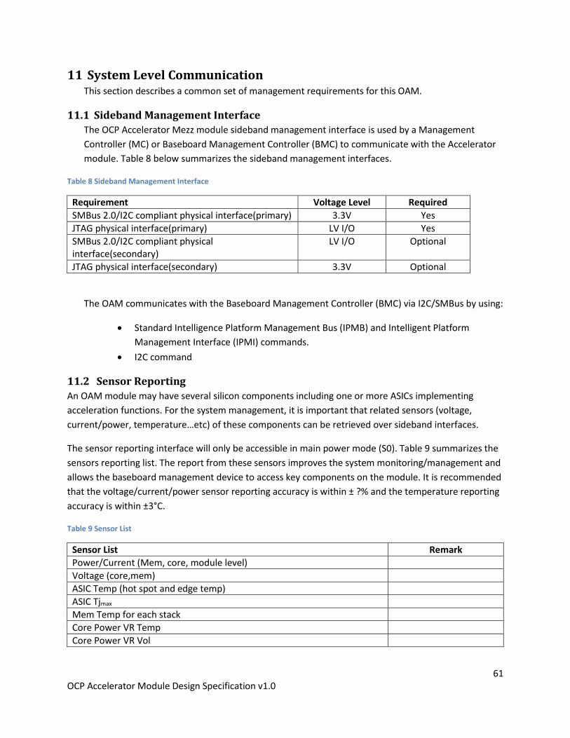
11.2 Sensor Reporting
An OAM module may have several silicon components including one or more ASICs implementing
acceleration functions. For the system management, it is important that related sensors (voltage,
current/power, temperature…etc) of these components can be retrieved over sideband interfaces.
The sensor reporting interface will only be accessible in main power mode (S0). Table 9 summarizes the
sensors reporting list. The report from these sensors improves the system monitoring/management and
allows the baseboard management device to access key components on the module. It is recommended
that the voltage/current/power sensor reporting accuracy is within ± ?% and the temperature reporting
accuracy is within ±3°C.
Table 9 Sensor List
Sensor List Remark
Power/Current (Mem, core, module level)
Voltage (core,mem)
ASIC Temp (hot spot and edge temp)
ASIC Tjmax
Mem Temp for each stack
Core Power VR Temp
Core Power VR Vol

62 OCP Accelerator Module Design Specification v1.0
Inlet sensor Need define common location
Outlet sensor
11.3 Error Monitoring/Reporting
System Management Controller (MC) or Baseboard Management Controller (BMC) shall be able to
monitor and access the accelerator module‘s internal registers as needed to set thresholds, clear status,
determine error counts and syndromes (SW driven interrupt or an Alert pin), and identify error
sources/Syndromes etc.
Mem
PCIe
ASIC
Interconnect Links
Others, I/O
11.4 Firmware Update
The accelerator module should support secure boot. The ASIC(s) needs to check signature of the
firmware each time it boots against keys programmed in OTP.
It will check using public keys burned into the silicon.
If the signature does not match, the chip will not boot.
Enter some sort of recovery mode allowing firmware to be flashed by the host.
Time-of-check-time-of-use (TOCTOU) attacks must be prevented. Specifically, host should NOT be able to modify firmware image once signature checks begin, and should also be unable to modify the stored or running firmware image after signature checks have been completed.
Key-revocation and anti-rollback protection must be provided for the accelerator firmware.
Protection against PDoS attacks must be provided.
Module supplier should provide the relevant tool for out-of-band firmware updates.
11.5 Power Capping
Module supplier should provide either the tool or I2C/IPMI commands to do power capping for the
module.
11.6 FRU Information
System Management Controller (MC) or Baseboard Management Controller (BMC) shall be able to
access related internal registers to get module information, such as vendor ID, device ID, Manufacturing
Serial number, firmware version, Bifurcation information, etc.
11.7 IO Calibration

63 OCP Accelerator Module Design Specification v1.0
System Management Controller (MC) or Baseboard Management Controller (BMC) shall be able to get
DDR/PCIe/interconnect training status and margin information. Special tools and API may need to be
provided by module vendors.

64 OCP Accelerator Module Design Specification v1.0
12 Environmental
12.1 Environmental Requirements
The OAM shall meet the following environmental requirements:
Gaseous Contamination: Severity Level G1 per ANSI/ISA 71.04-1985
Ambient operating temperature range: 5°C to +35°C
Operating and Storage relative humidity: 20% to 90% (non-condensing)
Storage temperature range: -20°C to +70°C
Transportation temperature range: -55°C to +85°C (short-term storage)
Operating altitude with no de-ratings: 3048m (10000 feet) – recommended as this is a Facebook
spec and standard for Telco operation
12.2 Regulation
The vendor needs to provide CB reports of the mezzanine module. These documents are needed to have
rack level CE. The OAM should be compliant with RoHS and WEEE. The PCB should have a UL 94V-0
certificate.

65 OCP Accelerator Module Design Specification v1.0
13 Revision History Author Description Revision Date
Whitney Zhao Initial Release 0.1 6/29/2018 Whitney Zhao Add pin list 0.2 11/09/2018 Tiffany Jin Cheng Chen
Update Mechanical, Thermal, Reliability sections Internal release
1/24/2019
Whitney Zhao Siamak Tavallaei
Add power profiles, power sequence requirement Update license information, overview
Internal release
2/4/2019
Tiffany Jin Whitney Zhao
Update module drawings Update pin list, recommended topologies
0.8 2/7/2019
Whitney Zhao Updated some typos, interconnect topologies Add LINK_CONFIG table
0.82
Tiffany Jin Update ME section 0.83
Cheng Chen Add liquid cooling concept drawing 0.84
Whitney Zhao Update license information. Update topology port mapping Add 156.25Mhz clock for Serdes
0.85
Whitney Zhao Tiffany Jin Cheng Chen
Update AFC interconnect topology routing recommendation to be compatible with HMC and FC Add management link routing guidance Update SerDes pin map Update ME drawings; more detail on requirements vs recommendations Add reference data for the increasing need of airflow for OAM cooling as die power increases
0.90
Whitney Zhao Change SerDes R to 7, update it from X20 to X16 Add two power reduction GPIO pins PWRRDT#[1:0] Add 8-port HCM topology and routing guide Update Vref range to 1.5V-3.3V Update section 8.6, add channel loss budget detail diagrams Update OAM_Pin_map to rev1.0: Detail change list pls refer to OAM_Pin_map_rev1.0 speadsheet; Update OAM_Pin_list to R1.0: detail change list pls refer to OAM_Pin_list_Rev1.0 spreadsheet
1.0