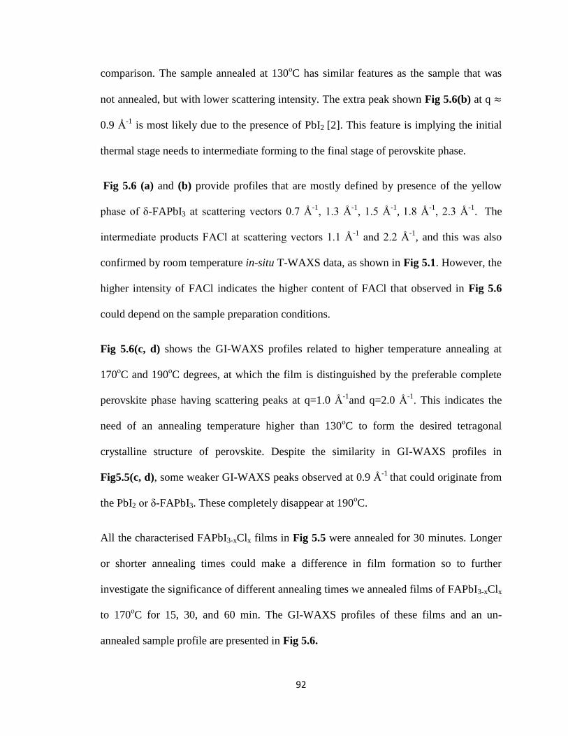
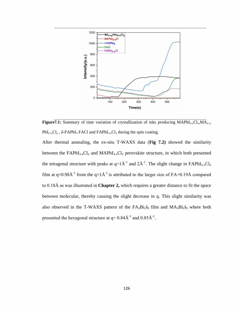
observation of crystal formation of halide perovskite thin
TRANSCRIPT

Observation of Crystal Formation of Halide Perovskite
Thin Films by Wide Angle X-ray Scattering
By
Noura Eid Alhazmi
A thesis submitted in partial fulfilment of the requirements for the degree of
Doctor of Philosophy
The University of Sheffield
Faculty of Engineering
Electronic and Electrical Engineering
August -2018
ii
Acknowledgements
Primarily I would like to express a considerable gratitude and appreciation to my
supervisor Dr Alan Dunbar for giving me the opportunity to undertake this work and all
his constructive comments time and patience Then I would like to thank Professor
Geraint Jewell for his encouragements and support Thank also goes to all the academic
and technical staff in University of Sheffield who didnrsquot hesitate to help me with this
project
The PhD project canrsquot be completed without accesses and the support from the Diamond
Light Centre to perform the WAXS experiments Therefore their helps and support are
appreciated
I thank my research group including Edwin Pineda De La O Konstantinos Tsevas
Gabriel E Perez Francesco Bastianini and Hatice Burak Furthermore all my friends
from Electronic and Electrical Engineering and the Physics departments deserve my
appreciation
My deep thanks to my beloved husband Dr Anas Alhazmi awesome sons Malik and
Mutaz lovely daughter Lara for all their patience and support and motivations Thank
also goes to Dr Khaled and his wife for all his advice and assistance Finally and
significantly I will not forget to thank all my brothers and sisters for their
encouragements and help
iii
Abstract
The perovskite solar cell received much attention due to its high power conversion
efficiency (PCE) and its easy and low cost fabrication process when compared to other
solar cell devices However the device was not commercialized because of perovskite
materials limitations related to fast decomposition in air sensitivity to humidity and
concerns about toxicity of the lead Therefore understanding the dynamics of perovskite
film forming for different material compositions will assist in overcoming these
perovskite materials limitations This is the main aim of this thesis
In situ spin coating wide angle X-ray scattering (WAXS) was not only used to investigate
MAPbI3-xClx films that were commonly applied but the different crystallization stages of
different perovskite material compositions were also studied in this project We observed
the faster crystallization of the intermediate product MAx+yPbI2+xCly after 2 minutes of
processing time
On the other hand slower crystallization of intermediate products was observed in
FAPbI3-xClx film formation compared to MAPbI3-xClx Noticeably the most important
finding related to FAPbI3-xClx perovskite film is the early forming stage of perovskite
phase before annealing
The WAXS investigation of lead free perovskite groups based on bismuth indicated the
fast crystallization of MA3Bi2I9 MA3Bi2I9ClX and FA3Bi2I9 materials during spin
coating However the surface coverage and optical band gap measurement of FA3Bi2I9
films placed it in the best candidate among other lead free materials
iv
Abbreviation
Ehv Energy of the photon
Eg Energy of band gap
VB Valence Band
CB Conduction Band
PCE Power Conversion Efficiency
NREL National Renewable Energy Laboratory
WAXS Wide angle X ray Scattering
GI-WAXS Grazing Incidence Wide Angle X-ray Scattering
T-WAXS Transmission Wide Angle X-ray Scattering
XRD X-ray Diffraction
SEM Scanning Electron Microscopy
UV-Vis Ultraviolet-Visible
MA Methylamine
FA Formamidine
MAI Methylammonium Iodide
FAI Formamidinium Iodide
DMF Dimethylformamide
PbCl2 Lead chloride
v
Contents
Acknowledgements ii
Abstract iii
Abbreviation iv
Chapter1 Introduction 1
11 Research Objective 1
12 Perovskite Solar Cells 3
13 Requirements of Photovoltaic Materials 5
14 References 7
Chapter 2 Theory and Literature Review 10
21 Perovskite Structure 10
22 Perovskite Solar Cell Devices 14
23 Fabrication processes of Perovskite Films 17
24 The properties of the Perovskite layers 19
241 Bandgap of Perovskite 19
242 Wide Angle X-ray Scattering (WAXS) of Perovskite Films 20
25 Toxicity of lead and alternative materials to lead 24
26 References 27
Chapter 3 Experimental Methods 34
31 Sample Preparation 35
vi
311 Perovskite Solution Preparation 35
312 Perovskite Film Preparation 36
32 Wide Angle X-ray Scattering WAXS 40
32-1 In situ Spin Coating T-WAXS Experiments 44
32-2 Grazing incidence Wide Angle Scattering GI-WAXS 47
32-3 The graphical presentation of WAXS Data 48
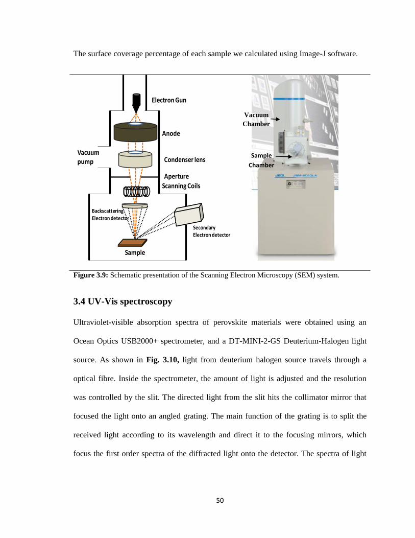
33 Scanning Electron Microscopy (SEM) 49
34 UV-Vis spectroscopy 50
35 References 53
Chapter 4 Dynamics of MAPbI3-xClx Perovskite Film Crystallization 56
41 In situ spin-coating of MAPbI3-xClx film 56
42 Crystalline Structure of Annealed MAPbI3-xClx Film Investigated by WAXS 66
43 Morphological Study of MAPbI3-xClx Film 69
44 UV-Vis spectra of MAPbI3-xClx Film 72
45 Air exposure effects on Annealed Film 73
46 Summary 77
47 References 77
Chapter 5 The Dynamics of FAPbI3-xClx Perovskite Films Crystallization 83
51 T-WAXS experiments during in-situ spin coating of the solution to produce FAPbI3-
xClx perovskite films 83
vii
52The Effects of Thermal Annealing on Crystallization of FAPbI3-xClx Perovskite films
90
52-1 Thermal Annealing Conditions of FAPbI3-xClx Film 90
52-2- Investigation of Surface Morphology of FAPbI3-xClx 95
52-3 Changes in Perovskite Crystalline Structure of FAPbI3-xClx Film After Thermal
Annealing 97
52-4 Degradation Study of FAPbI3-xClx Film by T-WAXS 100
53 Light Absorption Spectra of FAPbI3-xClx Film 103
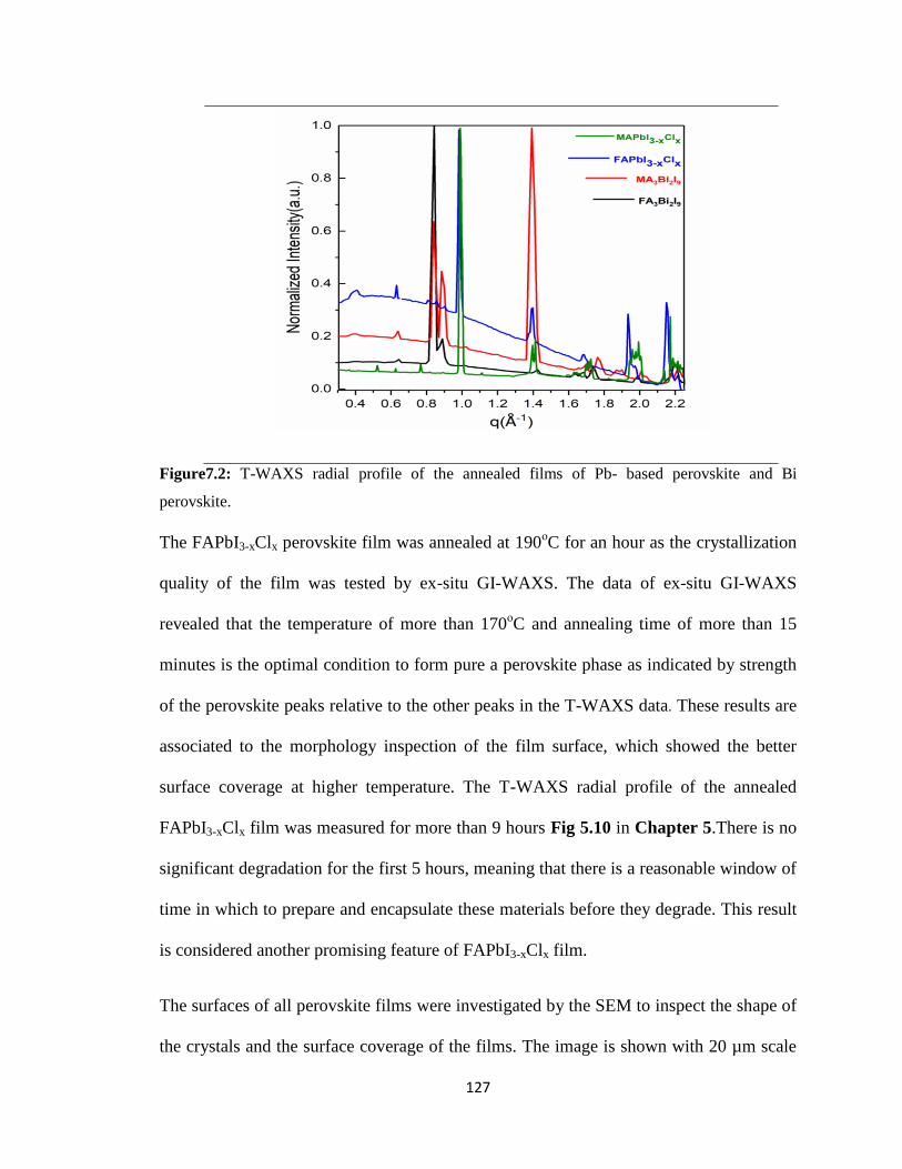
54 Conclusion 105
55 References 106
Chapter 6 Crystal formation of Lead Free Materials Related to Perovskite Based on
A3Bi2I9A3Bi2I9Clx 108
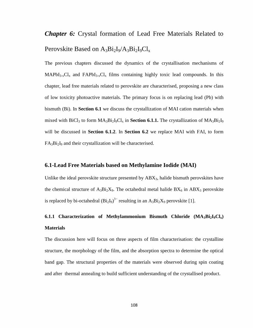
61-Lead Free Materials based on Methylamine Iodide (MAI) 108
611 Characterization of Methylammonium Bismuth Chloride (MA3Bi2I9Clx)
Materials 108
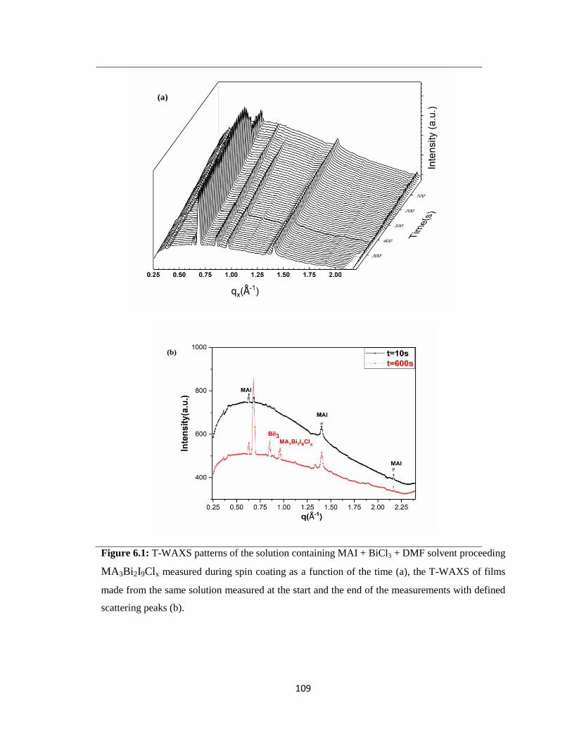
612 Characterization of Methylammonium Bismuth Iodide Materials (MA3Bi2I9) 113
62 Crystal Structural and Optical Properties of FA3Bi2I9 117
63 References 122
Chapter7 Conclusion 124
1
Chapter1 Introduction
The thesis objectives are introduced in this chapter in Section11 A brief discussion of
the development of the perovskite solar cell is presented in Section12 Clarification of
some requirements for the photovoltaic materials is given in Section13
11 Research Objective
With high expectations that nearly a third of the worldrsquos electricity will be generated by
photovoltaic technology from now to 2030 this technology is becoming a crucial subject
of research [1 2] Photovoltaic technology is defined as a technology that converts solar
energy into electricity and has been in development for over three generations
The first generation of solar cells mainly based on silicon (Si) wafers dominates the solar
cells market [3 4] The maximum efficiency of crystalline Si solar cell was 27 (as
reported by National Renewable Energy Laboratory (NREL)[5]
The second generation is defined as thin films solar cells that made of n-p type
semiconductors including cadmium telluride (CdTe) and gallium arsenide (GaAs) [6 7]
This technology recorded the best efficiency among other solar cells types as presented in
purple groups including the single solar cell and multi-junction solar cells in Fig11[6]
However the thin film solar cell technology requires advanced fabrication processes
These limitations lead to the emergence of the third generation technology that is defined
as the thin film solar cell based on a solution process[7]
2
Presently particular interest in the photovoltaic research focuses on this third generation
solar cells The third generation solar cell devices are organic photovoltaic dye sensitized
solar cells that are made from organics and organometal halide perovskite [3 4] In
comparison to organic photovoltaic and dye sensitized solar cells hybrid perovskite solar
cells produce higher efficiency with values more than 20 during a period of less than 10
years reporting in the literature and based on Fig11 [1 8 5] Despite the higher
efficiency of perovskite solar cells and the fast improvement compared to the other type
of solar cells the solar cell market progress is limited by perovskite material issues
including fast decomposition and high toxicity
In this thesis the main aim is to understand the hybrid perovskite better in order to
overcome these perovskite solar cells market limitations
3
Figure1 1 Power conversion efficiency of all solar cells based on inorganic and organic
materials as a function of the timeline from year 1975 to 2017 the circled data points highlight
the rapid growth in efficiency of the perovskite solar cells [5]
12 Perovskite Solar Cells
Most of the published reports regarding perovskite solar cells utilize the perovskite
materials MAPbI3 or MAPbI3-xClx as absorber materials as shown in Fig12[9]
However their large scale production may be limited by the toxicity of lead (Pb) as well
as material degradation that limits the lifetime of solar cells [9] Therefore further
4
investigation to find new perovskite materials is vital to overcome these limitations and
improve the efficiency of perovskite solar cells for use in a wide range of industries The
different new components of perovskite need to be sufficiently understood and carefully
characterized during the film formation process before use in solar cell devices The
dynamics of the crystallization stages during film forming is one of the important aspects
of perovskite films crystallization The efficiency of the perovskite solar cell can be
further increased by forming high quality crystalline films [10] Therefore the particular
aim of this project is to understand the crystallization stages of perovskite as these stages
occur during the film formation
Figure12 Power Conversion Efficiency (PCE) of perovskite solar cells as a function of the
timeline as reported in [9] Red bar =MAPbI3 Blue bar =MAPbI3-xClx and Green bar=mixed
perovskite
5
13 Requirements of Photovoltaic Materials
To operate the solar cells a photon of must be absorbed by an absorber layer Then the
generated carriers are transported and separated to extract free electrons out of the solar
cell into the external circuit [4]
The energy of the absorbed photon and the band gap of the semiconductor should be
considered In the case of the energy of the photon Ehv equal to the energy of the band
gap Eg of the absorber materials the electron can be promoted from the valence band
(VB) to the conduction band (CB) If the value of Ehvlt Eg the electron will not gain the
sufficient energy to be promoted to the conduction band and thus the exciton of an
electron-hole pair will not occur On the other hand photons with energy more than the
band gap energy can give electrons extra energy exciting them above the conduction
band edge These excited electrons then undergo electron relaxation (thermalization) to
the edge of the conduction band Therefore the energy of the band gap of the
photovoltaic materials should be carefully selected to absorb the photon energies within a
solar light and then form free carriers that generate electricity
In organometal halide perovskite the binding energy of the exciton is low in the range of
20-50meV comparable to thermal energy (25meV at room temperature) [11 12]
Therefore this binding energy facilitates breaking the exciton into free carriers
The correlation between the energy of the band gap of photovoltaic materials and PCE of
solar cells was studied and is shown by Shockley-Queisser (SQ) limit It can be observed
from the SQ limit that maximum power conversion more than 25 of the solar light can
6
be obtained by semiconductors having band gap 14eV such as GaAs[12] [13] Perovskite
having band gap between15 to 17 eV can yield around 20 PCE
Another preferable point in favour of GaAs is the direct band gap that increased the
ability to absorb solar light
Fig13 illustrates the difference between the direct and indirect band gap In the direct
band gap the energy of the photon is sufficient enough to promote an electron into the
conduction band whereas in indirect band gap materials an electron requires the
momentum of the phonon to move it into the conduction band and which also reduces
absorption effects
Figure13 The band structure of semiconductors illustrates (a) the direct band gap (b) the
indirect band gap
After light absorption and free carrier formation the generated carrier should be
separated and then collected by the cathode and anode in the external circuit to produce a
photocurrent[14] Carrier separation and transport requires materials with long diffusion
length
E
K
E
K
(a) (b)
EgEg
Ep
CB
VB
7
In perovskite materials the diffusion length of the carriers in the active layer (the
absorber material) is defined as the distance that carriers (free electron) can diffuse before
scattering becoming trapped or relaxing back to the VB
Therefore it must be long to prevent any chance of recombination between the electrons
and holes before arriving to the cathode and anode respectively In halide perovskite a
long diffusion length was observed at~100nm for lead iodide perovskites whereas in
mixed lead chloride halide perovskite it is even longer at ~1microm [15 16] In contrast in
the organic semiconductor materials this value is in the range of only 20 nm limiting the
efficiency of the organic solar cells[16]
In solution processed solar cells it is important to ensure that good surface coverage with
the photovoltaic material is achieved In this thesis we will study how the surface
coverage of perovskite films can be varied based on the thermal annealing conditions
A brief background of the origin of the perovskite materials and their related attractive
properties is presented in Chapter 2 Details of the sample preparation and experimental
steps are discussed in Chapter 3 The conventional material MAPbI3-xClx is
characterized in Chapter 4 and Chapter 5 focuses on analysis and characterization of
FAPbI3-xClx Lead free materials incorporating MA and FA cations mixed with BiI3 and
BiCl3 are studied in Chapter 6
14 References
1 Green MA A Ho-Baillie and HJ Snaith The emergence of perovskite solar cells
Nature Photonics 2014 8(7) p 506-514
8
2 Turner G Global Renewable Energy Market Outlook 2013 Bloomberg New
Energy Finance httpswwwbnefcominsightdownload7526pdf (11 April 2014
2013
3 Green MA Third generation photovoltaics solar cells for 2020 and beyond
Physica E Low-dimensional Systems and Nanostructures 2002 14(1) p 65-70
4 Yan J and BR Saunders Third-generation solar cells a review and comparison
of polymer fullerene hybrid polymer and perovskite solar cells RSC Advances 2014
4(82) p 43286-43314
5 NERL httpswwwnrelgovncpvimagesefficiency_chartjpg 2017
6 Green MA K Emery Y Hishikawa W Warta and ED Dunlop Solar cell
efficiency tables (version 48) Progress in photovoltaics research and applications 2016
24(7) p 905-913
7 Kazim S MK Nazeeruddin M Graumltzel and S Ahmad Perovskite as light
harvester a game changer in photovoltaics Angewandte Chemie International Edition
2014 53(11) p 2812-2824
8 Luo S and WA Daoud Recent progress in organic-inorganic halide perovskite
solar cells mechanisms and material design Journal of Materials Chemistry A 2015
3(17) p 8992-9010
9 Elumalai NK MA Mahmud D Wang and A Uddin Perovskite Solar Cells
Progress and Advancements Energies 2016 9(11) p 861
10 Barrows AT S Lilliu AJ Pearson D Babonneau AD Dunbar and DG
Lidzey Monitoring the Formation of a CH3NH3PbI3ndashxClx Perovskite during Thermal
9
Annealing Using X‐Ray Scattering Advanced Functional Materials 2016 26(27) p
4934-4942
11 Niu G X Guo and L Wang Review of recent progress in chemical stability of
perovskite solar cells Journal of Materials Chemistry A 2015 3(17) p 8970-8980
12 Polman A M Knight EC Garnett B Ehrler and WC Sinke Photovoltaic
materials Present efficiencies and future challenges Science 2016 352(6283)
13 Shockley W and HJ Queisser Detailed balance limit of efficiency of p‐n
junction solar cells Journal of applied physics 1961 32(3) p 510-519
14 Nelson J The physics of solar cells 2003 World Scientific Publishing
Company
15 Stranks SD GE Eperon G Grancini C Menelaou MJ Alcocer T Leijtens
LM Herz A Petrozza and HJ Snaith Electron-hole diffusion lengths exceeding 1
micrometer in an organometal trihalide perovskite absorber Science 2013 342(6156) p
341-344
16 Xing G N Mathews S Sun SS Lim YM Lam M Graumltzel S Mhaisalkar
and TC Sum Long-range balanced electron-and hole-transport lengths in organic-
inorganic CH3NH3PbI3 Science 2013 342(6156) p 344-347
10
Chapter 2 Theory and Literature Review
This chapter presents a brief review of theoretical background and some relevant
previous work that study organometal halide perovskite films In Section 21 the structure
of origin of the organometal halide perovskite is discussed whereas Section 22 focuses
more on the perovskite solar cell devices Some perovskite film fabrication techniques
are summarized in Section 23 The perovskite studies of band gap and studies related to
WAXS are detailed in Section 24 and finally a brief discussion of the lead free materials
related to perovskite is presented in Section 25
21 Perovskite Structure
The name is referred to the Russian mineralogist Lev A Perovskie who characterized the
structure of perovskite materials [1 2] Perovskite is defined as the large family of
crystalline materials with a similar cubic structure to calcium titanium oxide (CaTiO3)
that is generally expressed as ABX3 [3 4]
The A cation determines whether the perovskite is organic or inorganic In organometal
halide perovskite group A is organic The smaller size and non- spherical structure of
organic A cation is crucial to form 3D symmetric perovskite [1 5]
Halide perovskites with halogen anionic components (Fe Br Cl and I) have received
more attention because of their more suitable band gap which generally does not exceed
25eV [6] In contrast the oxide perovskite categories with general chemical formula
ABO3 are described as transparent materials with wide band gap 3-5eV wider than the
solar spectrum [7-9]
11
The ideal cubic unit cell of the halide organic perovskite is depicted in Fig 21 The B
component (of the ABX3 structure) bonds to the six corners of X forming BX6 octahedra
Each octahedra then forms a corner of a cube where the A organic cation fills the gap
between the four octahedrs to form a cubic structure [4 6 10]
Figure21 The cubic symmetry of the organic-inorganic perovskite unit cell [11]
The size of each compound determines the ideal geometry of the unit cell of its organic
halide perovskite Tolerance (t) and octahedra (micro) factors define the correlation between
the radii size of A B and X and the geometry of the unit cell The tolerance factor is
defined based on the radii size of RA RB and Rx as can be seen in Eq21 whereas the
value of the octahedral factor is defined by the ratio of the radii size of the metal RB and
halide cation Rx as shown in Eq22[12]
A cubic structure that is crystallographically stable is formed if the tolerance value is in
the range 081lttlt111 [11] Values smaller than 081 form a structure with lower
symmetry than the cubic structure such as tetragonal or orthorhombic structures [11] A
tolerance factor greater than 111 will destroy the 3D framework of the unit cell [1] The
12
octahedra factor is related to the shape of the BX6 octahedral Preferable values of
044ltmicrolt090 express the halide perovskite structure
The tolerance and octahedra factors of some perovskite materials were calculated based
on the radii size of A B and X of perovskite materials in literature see Table 21 [1] The
study compares several perovskite materials based on four cations cesium (Cs)
methylammonium (MA) formamidinium (FA) and ethylammonium (EA) mixed with Pb
and Sn as metal cations and I Cl and Br as halide anions In this thesis the halide
perovskites are discussed composed of MA and FA cations and Pb and Bi as metals
where the halide anion I and IxCl3-x
The larger A cation forms a structure closer (t) to the unit such as FA and EA and a
lower symmetry structure is more likely to be obtained by smaller cations MA and Cs as
illustrated in Fig 22 A large cation A is most likely to result in a cubic structure
However a high tolerance factor alone as it is the case for ethylammonium (EA) is still
not a sufficient factor to be used widely in solar cells due to the wider band gap than the
optimum range [13] Solar cells based on EA perovskite materials produce a PCE of only
22[14] Therefore the FA cation is more suitable than MA and EA to form a cubic
perovskite
13
Ions Materials R(nm)
A (Organic cation)
MA 018
EA 023
FA 019~022
B (Metal cation ) Pb 0119
Sn 011
X (Halogen anion) I 022
Cl 0196
Br 018
Table 21 The ionic radii size of the A B and X as shown in [1] based on the values reported in
[15-18]
In addition to the importance of selecting the suitable compounds during the synthesis of
organicndashhalide perovskite to form a structural stability there are several other factors can
change the structure of the materials prepared from the same components For example
MAPbI3 exhibits a tetragonal structure at room temperature but annealing the film at
100оC can change the structure from tetragonal to cubic where the lower temperature
causes opposite effect see Fig 23 [19]
14
Figure 22The calculated tolerance factor and octahedral factors for some organic ndashinorganic
perovskite components [1]
Figure 23 Crystal structure of MAPbI3 that exhibits cubic and tetragonal symmetry as reported
in[19]
22 Perovskite Solar Cell Devices
The first emergence of organic inorganic halide perovskite as a photovoltaic material was
in a dye sensitized solar cells (DSSC) as a replacement of the organic dye and showed a
EA
Cs
FA
MA
15
PCE of only 22 in 2006[20] The same group (Kojima A and co-workers) in 2009
optimized the halogen in the halide organic perovskite materials by replacing iodine (I)
with bromide (Br) This yielded an enhancement in the PCE from 22 to 38 due to
the change in the band gap [17] However besides the low performance of DSSC
perovskite solar cells the main issue is the short life time caused by dissolving the
perovskite in the liquid electrolyte In addition further enhancement to perovskite solar
cells was carried out in 2012 by replacing the liquid electrolyte with solid state hole
transporting materials HTM which caused an increase in PCE to 97 and improved the
stability of the solar cell [21]
In 2013 a striking increase in PCE from 42 to 122 was recorded when the
perovskite based on mixed halide perovskite was used as an absorber layer in planer
heterjunction[22] The main advantage of mixed halide perovskite is the longer diffusion
length which minimizes the risk of the electron-hole recombination Another important
contribution reported by the same group involved using a two evaporation source to
deposit the perovskite layer which provides higher film surface coverage as detailed in
the next section and therefore higher PCE was recorded at 154[23]
Using a DMSO solvent in perovskite preparation instead of the common solvent DMF
led to further increases in the PCE to more than 16 in 2014 [24]
For the perovskite materials mixing the organic cations FA and MA caused preferable
performance of the perovskite solar cell to reach 184 [25] Similar research was carried
out on mixed materials using FAPbI3 and MAPbBr3 perovskite materials and the
intermolecular exchanges method enhanced PCE to greater than 20[26] Several
16
optimisations were reported after that resulting in very high performance of perovskite
solar cell devices with more than 21 efficiency recorded in 2016 [27]
Principle of the operation of perovskite solar cells varies from architecture to another our
discussion will be restricted to simple planar architecture As with any solar cell
perovskite solar cells aim to convert sunlight into electrical energy This can be achieved
by light absorption charge separation and charge collection that are considered the three
fundamental processes of the solar cell devices
Under sunlight conditions the light is absorbed by the perovskite layer The thin flat
layer of perovskite works as a light absorber and because of the low binding energy of the
exciton (20-50meV) electron and hole separate immediately into free charges as was
introduced in Section 13 in Chapter 1
Since the conduction band level in the electron transporting materials (ETM) is very
close to the one in the perovskite layer (eg MAPbI3 -39eV) the electron will be injected
into ETM
The hole transporting the materials (HTM) had high hole mobility and the valence band
matched with the valence band of the perovskite (eg MAPbI3 -55eV) to work to
transport the hole collected by the anode
Fig24 illustrates the structure of the perovskite solar cells and the band diagram where
the materials were selected based on the band diagram
17
Figure 24 Architecture of a planar perovskite solar cells device (a) and (b) the band diagram
of the same materials showing where electrons travel through the conduction band (CB) of the
electron transporting materials and the holes travel via the valence band (VB) of the hole
transporting materials and charges may be collected by the selective contacts
Despite the optimisation in the structure of the device and the layers of the carriers
transporting materials still the perovskite solar cell market progress of perovskite solar
cells can be limited by perovskite material issues [11]
Main issues are the toxicity of the lead in perovskite and the fast degradation of
perovskite that cause short solar cells lifetime Therefore material optimisation with
complete understanding of perovskite film formation will be important aspects of the
research related to the perovskite solar cells
23 Fabrication processes of Perovskite Films
Perovskite films can be prepared by several methods The most commonly used is spin
coating [28 29] In a single step a suitable solvent is used to prepare a well dissolved
solution that contains A B and X This can be prepared in one step and then deposited
onto a substrate as shown in Fig 25 (a) It can also be done in two steps where the
+
-
+- +
+
+
--
Perovskite
ETM
HTM
Anode
Transparent
Cathode glass
(a) (b)
E(e
V)
-39
-55
-44
VB
-55
AgFTO
CB
Solar light
18
solution contains PbI2 or PbCl2 (solution 1) deposited first then another solution
containing MAI (solution 2) deposited next followed by spin coating [13] Dipping
techniques were also reported where after depositing the solution 1 the film was dipped
into solution 2 to form the perovskite film Fig 25(b)
Pinhole free perovskite films have been prepared with more advanced techniques such as
vacuum deposition using dual sources where both MAI and PbI or PbICl are evaporated
onto the substrate Fig 25(c) or alternately using a single source system where only MAI
is evaporated onto a PbI layer Fig 25(d) The morphology of the perovskite films
prepared by vapor deposition and the solution were researched with the results shown in
Fig 26[30]
Although the techniques yield high morphology it is difficult to apply for large-scale
industrial needs and the vacuum evaporation source is relatively expensive compared to
spin coating [31]
Figure 25 Several methods used to make perovskite films including (a) spin coating single step
(b) two steps and vacuum evaporation (c) with dual source and (d) with single source[32]
19
Figure 26 The surface of perovskite film prepared (a) by vapour deposition using dual source
and (b) solution processes illustrated in [30]
24 The properties of the Perovskite layers
The discussion is restricted on band gap of the perovskite film and the high crystallization
properties that influence on the performance of the solar cell device
241 Bandgap of Perovskite
The band gap is formed between the conduction band formed by Pb 6p orbital and the
valence band formed from Pb 6sndashI 5p [33 34] The transition between the lower point of
conduction band and the highest point of the valence band should ideally be a direct
band gap with strong optical absorption[13] as is the case in GaAs (introduced in
Section 13)
Changing the halide anion from I to Br causes some alteration in the optical absorption
spectra and diffusion length It was observed for example that one could tune the optical
band gap and absorption spectra of MAPb(I1-xBrx)3 when the amount of Br changed as
shown in Fig 27[35]
20
Figure 27 Optical absorption of MAPb(I1-xBrx)3 films when x changes from 0 to 1in (a) and the
photographs of the same films (b) [35]
242 Wide Angle X-ray Scattering (WAXS) of Perovskite Films
Previously Wide angle X-ray Scattering (WAXS) has been used to investigate different
aspects of the perovskite films Ex-situ WAXS with grazing incident angle was used in
order to compare between the one-step and tow-step process solution of spin coating[36]
In one step solution the lead salt and the organic cation dissolve together in one solution
and deposit on the surface of the substrate whereas in the tow steps the lead and organic
cation dissolved individually to deposit the mixture of the lead salt with solvent then at
the next step the solution of the organic cation with solvent The experimental study
concluded no significant difference was observed However the high crystallization of
the perovskite film prepared by the two step process relies on the uniformity of the Pb
layer that is formed first as was detailed previously
21
MAPbI3-xClx perovskite solar cells were thermally annealed in situ to investigate the
phase transition from the precursor phase into the perovskite phase and its degradation
products [37 38] In both reports cited annealing at 80оC for 120 minutes is defined as
being sufficient to obtain the perovskite phase while more than 2hr causes
decomposition of the perovskite and at temperature lower than these conditions only the
precursor phase to be formed In one report perovskite solar cells were made using a
range of thermal annealing conditions and higher efficiency was obtained when the
perovskite film was annealed for 120 min (PCE12) whereas only 78 PCE recorded
from 80min annealing time [37] This suggests that forming a good quality crystalline
perovskite film is one of the essential criteria to obtaining the high solar cell efficiency
Fig 28 shows the results of GI-WAXS and the morphology of perovskite films
Figure 28 The result of the GI-WAXS of Scanning electron microscopy (SEM) images of films
annealed for time periods the surface of the films investigated by SEM a) 60min b) 80 min c)
100 min d) 120 min e) 140 min and f) 180 min where scale bars correspond to 1 μm as was
reported in [37]
22
The finding of this study are in agreement with a similar study which reported that MAI
PbCl3 perovskite films have three crystallization dynamics stages[39] The first stage
observed is the precursor stage at the early thermal annealing after 5 min at 35 C Only
intermediate products formed at this stage The perovskite phase formed after 100 min
when the chemical reaction was complete During the final stage decomposition of
perovskite into lead salt was observed and the intermediate phase was recorded after
150min as illustrated in Fig 29
23
Figure 29 the three crystallization stages of the perovskite a) the precursor stage where the
intermediate products are formed b) the perovskite stage and c) the decomposition where the
perovskite is decomposed into the lead salt and intermediate
However the dynamic crystallization during spin coating of perovskite film has not yet
been investigated and reported which would further understanding of the crystal
formation in perovskite films unclear at this stage
24
25 Toxicity of lead and alternative materials to lead
The most common perovskite materials investigated in the literature includes Pb2+
which
yields very high PCEs exceeding 20[40] However the mass production of such
materials in the future may well be limited by the toxicity of the lead Pb2+
ion which is
highly soluble in water [41] Therefore it is important that a research solution to this
issue is found This could be achieved by suitable encapsulation and disposal at the end
of life devices but preferably further research in the organometal halide perovskite field
will make it possible to replace it
Bismuth (Bi) can be used to substitute Lead (Pb)
due to its similar electronic
configuration and better stability than Tin (Sn) that was also used [42 43] Fig 210 (a)
shows the colour of the different films of MBI films that were prepared from Bi and MAI
and conventional films of MAPbI3 during 26 days The colour of the Bi-perovskite films
was unchanged after 13 days and turned into the brighter colour film only after 26 days
that indicates a high air stability as compared to the MAPbI3 which changed from the
dark brown to yellow after 13 days[44]
The XRD pattern of MBI films measured in the same study within 26 days is shown in
Fig 210(b)[44] A very slight change in the structure of the film was observed after 26
days as indicated by the structure stability in air and humidity condition 61
The optical absorption of Bi mixed with Cs materials (investigated over the course of 30
days in a different study) showed almost the same spectra Fig 210(e) [45]
25
Figure 210 The crystal structure in XRD of MBI in (a-d) and colour of film in (c) as reported in
[44] the optical absorption of BiI mixed with Cs materials in(e) [45]
The chemical structure of Bi halide perovskite is quite different than the ideal halide
perovskite structure ABX3 In the organometal halide perovskite a metal halide BX6 layer
is formed as octahedral and A cation fills the space in the middle of cubic of formed from
octahedral shape Replacing Pb2+
to Bi3+
causes the change in the B-X bond and metal
halide octahedral PbI6 can be replaced by Bi-octahedral (Bi2 I9)-3
surronding by the A
cation as illustrated in Fig 211[46 43]
The progress of Bi perovskite solar cell still materials is not at a competitive level with
the halide lead perovskite solar cells where the maximum efficiency reported is 215
PCE [43]Therefore this part of the study still needs further research and understanding
before the materials can help modify the perovskite solar cell efficiency
(E)
26
Figure 211 Structure of A3Bi2X9 as reported in [43]
In summary the chapter includes brief relative research work related to perovskite
materials which can be instructive in highlighting some points The preferable structure
of the cubic organometal halide perovskite is related to the size of the A B and X and FA
cation can be considered as a more suitable candidate than MA and EA
The performance of the perovskite solar cell can be further enhanced by using a highly
pure crystallised perovskite film as the absorber layer This was shown by assessment
after in situ thermal annealing however in situ WAXS of spin coating has not yet been
investigated for comparison Therefore the current project will focus on in situ WAXS
analysis of spin coated perovskite films
The final discussed point is the stability of perovskite solar cell based on Bi instead of Pb
as its attractive aspects suggest that Bi can be used to make less toxic material and also
allow operate the solar cell for a longer life time However materials based on Bi also
Bi
A
X
27
need to be studied to more fully understand them and in order to bring them a level
competitive with the lead perovskite solar cell
26 References
1 Chen Q N De Marco Y Yang T-B Song C-C Chen H Zhao Z Hong and
H Zhou Under the spotlight The organicndashinorganic hybrid halide perovskite for
optoelectronic applications Nano Today 2015 10(3) p 355-396
2 Gao P M Graumltzel and MK Nazeeruddin Organohalide lead perovskites for
photovoltaic applications Energy amp Environmental Science 2014 7(8) p 2448-
2463
3 Hsiao Y-C T Wu M Li Q Liu W Qin and B Hu Fundamental physics
behind high-efficiency organo-metal halide perovskite solar cells Journal of
Materials Chemistry A 2015 3(30) p 15372-15385
4 Luo S and WA Daoud Recent progress in organic-inorganic halide perovskite
solar cells mechanisms and material design Journal of Materials Chemistry A
2015 3(17) p 8992-9010
5 Kazim S MK Nazeeruddin M Graumltzel and S Ahmad Perovskite as light
harvester a game changer in photovoltaics Angewandte Chemie International
Edition 2014 53(11) p 2812-2824
6 Niu G X Guo and L Wang Review of recent progress in chemical stability of
perovskite solar cells Journal of Materials Chemistry A 2015 3(17) p 8970-
8980
28
7 Bhatnagar A AR Chaudhuri YH Kim D Hesse and M Alexe Role of
domain walls in the abnormal photovoltaic effect in BiFeO3 Nature
Communications 2013 4
8 Choi T S Lee Y Choi V Kiryukhin and S-W Cheong Switchable
ferroelectric diode and photovoltaic effect in BiFeO3 Science 2009 324(5923)
p 63-66
9 Ji W K Yao and YC Liang Bulk photovoltaic effect at visible wavelength in
epitaxial ferroelectric BiFeO3 thin films Advanced Materials 2010 22(15) p
1763-1766
10 Sum TC and N Mathews Advancements in perovskite solar cells photophysics
behind the photovoltaics Energy amp Environmental Science 2014 7(8) p 2518-
2534
11 Green MA A Ho-Baillie and HJ Snaith The emergence of perovskite solar
cells Nature Photonics 2014 8(7) p 506-514
12 Li C X Lu W Ding L Feng Y Gao and Z Guo Formability of ABX3 (X=
F Cl Br I) Halide Perovskites Acta Crystallographica Section B Structural
Science 2008 64(6) p 702-707
13 Elumalai NK MA Mahmud D Wang and A Uddin Perovskite Solar Cells
Progress and Advancements Energies 2016 9(11) p 861
14 Im J-H J Chung S-J Kim and N-G Park Synthesis structure and
photovoltaic property of a nanocrystalline 2H perovskite-type novel sensitizer
(CH3CH2NH3) PbI3 Nanoscale Research Letters 2012 7(1) p 353
29
15 Baikie T Y Fang JM Kadro M Schreyer F Wei SG Mhaisalkar M
Graetzel and TJ White Synthesis and crystal chemistry of the hybrid perovskite
(CH 3 NH 3) PbI 3 for solid-state sensitised solar cell applications Journal of
Materials Chemistry A 2013 1(18) p 5628-5641
16 Fan Z K Sun and J Wang Perovskites for photovoltaics a combined review of
organic-inorganic halide perovskites and ferroelectric oxide perovskites Journal
of Materials Chemistry A 2015 3(37) p 18809-18828
17 Kojima A K Teshima Y Shirai and T Miyasaka Organometal Halide
Perovskites as Visible-Light Sensitizers for Photovoltaic Cells Journal of the
American Chemical Society 2009 131(17) p 6050-6051
18 McKinnon NK DC Reeves and MH Akabas 5-HT3 receptor ion size
selectivity is a property of the transmembrane channel not the cytoplasmic
vestibule portals The Journal of General Physiology 2011 138(4) p 453-466
19 Luo S and WA Daoud Crystal Structure Formation of CH3NH3PbI3-xClx
Perovskite Materials 2016 9(3) p 123
20 Kojima A Teshima K Miyasaka T amp Shirai Y Novel photoelectrochemical
cell with mesoscopic electrodes sensitized by lead-halide compounds (2) 210th
ECS Meeting (ECS 2006) 2006
21 Kim H-S C-R Lee J-H Im K-B Lee T Moehl A Marchioro S-J Moon
R Humphry-Baker J-H Yum and JE Moser Lead iodide perovskite sensitized
all-solid-state submicron thin film mesoscopic solar cell with efficiency
exceeding 9 Scientific reports 2012 2 p 591
30
22 Stranks SD GE Eperon G Grancini C Menelaou MJ Alcocer T Leijtens
LM Herz A Petrozza and HJ Snaith Electron-hole diffusion lengths
exceeding 1 micrometer in an organometal trihalide perovskite absorber Science
2013 342(6156) p 341-344
23 Liu M MB Johnston and HJ Snaith Efficient planar heterojunction
perovskite solar cells by vapour deposition Nature 2013 501(7467) p 395
24 Jeon NJ JH Noh YC Kim WS Yang S Ryu and SI Seok Solvent
engineering for high-performance inorganicndashorganic hybrid perovskite solar cells
Nature materials 2014 13(9) p 897-903
25 Jeon NJ JH Noh WS Yang YC Kim S Ryu J Seo and SI Seok
Compositional engineering of perovskite materials for high-performance solar
cells Nature 2015 517(7535) p 476
26 Yang WS JH Noh NJ Jeon YC Kim S Ryu J Seo and SI Seok High-
performance photovoltaic perovskite layers fabricated through intramolecular
exchange Science 2015 348(6240) p 1234-1237
27 Saliba M T Matsui J-Y Seo K Domanski J-P Correa-Baena MK
Nazeeruddin SM Zakeeruddin W Tress A Abate A Hagfeldt and M
Gratzel Cesium-containing triple cation perovskite solar cells improved stability
reproducibility and high efficiency Energy amp Environmental Science 2016 9(6)
p 1989-1997
28 Jeon NJ JH Noh WS Yang YC Kim S Ryu J Seo and SI Seok
Compositional engineering of perovskite materials for high-performance solar
cells Nature 2015 517(7535) p 476-480
31
29 Zhou H Q Chen G Li S Luo T-b Song H-S Duan Z Hong J You Y
Liu and Y Yang Interface engineering of highly efficient perovskite solar cells
Science 2014 345(6196) p 542-546
30 Liu M MB Johnston and HJ Snaith Efficient planar heterojunction
perovskite solar cells by vapour deposition Nature 2013 501(7467) p 395-398
31 Bai S Z Wu X Wu Y Jin N Zhao Z Chen Q Mei X Wang Z Ye T
Song R Liu S-t Lee and B Sun High-performance planar heterojunction
perovskite solar cells Preserving long charge carrier diffusion lengths and
interfacial engineering Nano Research 2014 7(12) p 1749-1758
32 Heo JH DH Song BR Patil and SH Im Recent progress of innovative
perovskite hybrid solar cells Israel Journal of Chemistry 2015 55(9) p 966-977
33 Koutselas I L Ducasse and GC Papavassiliou Electronic properties of three-
and low-dimensional semiconducting materials with Pb halide and Sn halide
units Journal of Physics Condensed Matter 1996 8(9) p 1217
34 Stoumpos CC and MG Kanatzidis The renaissance of halide perovskites and
their evolution as emerging semiconductors Accounts of chemical research
2015 48(10) p 2791-2802
35 Noh JH SH Im JH Heo TN Mandal and SI Seok Chemical management
for colorful efficient and stable inorganicndashorganic hybrid nanostructured solar
cells Nano letters 2013 13(4) p 1764-1769
36 Schlipf J P Docampo CJ Schaffer V Koumlrstgens L Bieszligmann F Hanusch
N Giesbrecht S Bernstorff T Bein and P Muumlller-Buschbaum A Closer Look
32
into Two-Step Perovskite Conversion with X-ray Scattering The journal of
physical chemistry letters 2015 6(7) p 1265-1269
37 Barrows AT S Lilliu AJ Pearson D Babonneau AD Dunbar and DG
Lidzey Monitoring the Formation of a CH3NH3PbI3ndashxClx Perovskite during
Thermal Annealing Using X‐Ray Scattering Advanced Functional Materials
2016 26(27) p 4934-4942
38 Tan KW DT Moore M Saliba H Sai LA Estroff T Hanrath HJ Snaith
and U Wiesner Thermally induced structural evolution and performance of
mesoporous block copolymer-directed alumina perovskite solar cells Acs Nano
2014
39 Moore DT H Sai KW Tan D-M Smilgies W Zhang HJ Snaith U
Wiesner and LA Estroff Crystallization kinetics of organicndashinorganic trihalide
perovskites and the role of the lead anion in crystal growth Journal of the
American Chemical Society 2015 137(6) p 2350-2358
40 Bi D W Tress MI Dar P Gao J Luo C Renevier K Schenk A Abate F
Giordano and J-PC Baena Efficient luminescent solar cells based on tailored
mixed-cation perovskites Science advances 2016 2(1) p e1501170
41 Noel NK SD Stranks A Abate C Wehrenfennig S Guarnera A-A
Haghighirad A Sadhanala GE Eperon SK Pathak and MB Johnston Lead-
free organicndashinorganic tin halide perovskites for photovoltaic applications
Energy amp Environmental Science 2014 7(9) p 3061-3068
42 Kwak CK AT Barrows AJ Pearson DG Lidzey and AD Dunbar An X-
ray scattering and electron microscopy study of methylammonium bismuth
33
perovskites for solar cell applications Journal of Materials Research 2017
32(10) p 1888-1898
43 Park BW B Philippe X Zhang H Rensmo G Boschloo and EM
Johansson Bismuth based hybrid perovskites A3Bi2I9 (A methylammonium or
cesium) for solar cell application Advanced Materials 2015 27(43) p 6806-
6813
44 Hoye RL RE Brandt A Osherov V Stevanović SD Stranks MW Wilson
H Kim AJ Akey JD Perkins and RC Kurchin Methylammonium bismuth
iodide as a lead‐free stable hybrid organicndashinorganic solar absorber Chemistry-A
European Journal 2016 22(8) p 2605-2610
45 Eckhardt K V Bon J Getzschmann J Grothe FM Wisser and S Kaskel
Crystallographic insights into (CH 3 NH 3) 3 (Bi 2 I 9) a new lead-free hybrid
organicndashinorganic material as a potential absorber for photovoltaics Chemical
Communications 2016 52(14) p 3058-3060
46 Lyu M J-H Yun M Cai Y Jiao PV Bernhardt M Zhang Q Wang A Du
H Wang G Liu and L Wang Organicndashinorganic bismuth (III)-based material
A lead-free air-stable and solution-processable light-absorber beyond organolead
perovskites Nano Research 2016 9(3) p 692-702
34
Chapter 3 Experimental Methods
As was stated in Chapter 1 this thesis aims to investigate the dynamic crystallisation of
different categories of organic halide perovskite materials used in solar cell devices In
order to achieve this aim several experimental methods were used to characterize the
materials
The materials preparation methods are discussed in Section 31 and the characterization
tools involve the interaction of matter with X-rays electrons and Ultraviolet-visible light
Section 32 presents the work of X-ray scattering and diffraction physics to identify the
formation mechanism of the crystalline products in perovskite film during the spin
coating processes using in situ spin coating wide angle X-ray scattering WAXS
experiments
In Chapter 5 grazing incidence wide angle X-ray scattering (GI-WAXS) is applied to
study the effects of the thermal annealing on the crystalline structure of FAPbI3-xClx
perovskite films Therefore the GI-WAXS procedure will be discussed in Section 32-2
The surface morphology and crystallization of perovskite films were investigated using
scanning electron microscopy (SEM) which will be described in Section 33 Section 34
will explain how light absorption and the optical band gap were measured using UV-Vis
spectroscopy
35
31 Sample Preparation
311 Perovskite Solution Preparation
In this thesis three categories of perovskite materials were investigated The first
category is perovskite based on methylammonium lead iodide chloride (MAPbI3-xClx)
The formamidinium lead iodide chloride (FAPbI3-xClx) perovskite is the second category
which both categories detailed in Chapter 4 and Chapter 5 The third group is the lead-
free materials related to perovskite category that was also investigated including
MA3Bi2I9-xClx and the composition of bismuth iodide with FA and MA which form
FA3Bi2I9 and MA3Bi2I9 perovskite respectively The FA and MA cations are
abbreviations of NH2CH=NH2 and CH3NH3 respectively Lead-free perovskite will be
discussed in Chapter 6
The simple one-step solution preparation mechanism that was detailed in Chapter 2 was
applied to prepare all perovskite solutions as was described in the literature [1 2]
To prepare the perovskite MAPbI3-xClx solution methylammonium iodide (MAI) and
lead chloride (PbCl2) were mixed in a 31 molar ratio The MAI and PbCl2 were
purchased from Sigma-Aldrich The 31 molar ratio was selected because in the literature
it obtained high quality perovskite materials [3 4] The mixture was dissolved in
anhydrous dimethylformamide (DMF) that were purchased from Sigma-Aldrich to form a
32 M solution
Similarly the FAPbI3-xClx ink was prepared by mixing formamidinium iodide (FAI)
which was purchased from Ossila Ltd and lead chloride (PbCl2) purchased from Sigma-
36
Aldrich in a 31 molar ratio The mixture was then dissolved in anhydrous DMF to form
a 32 M solution To avoid the toxicity associated with lead in the perovskite materials
bismuth chloride (BiCl3) and bismuth iodide (BiI3) were applied instead of lead chloride
(PbCl2) BiCl3 supplied by Acros Organics was mixed with MAI using the same 31
molar ratio and the same DMF solvent to form a 32 M solution of MA3Bi2I9Clx
FA3Bi2I9 and MA3Bi2I9 solutions were prepared by mixing bismuth iodide (BiI2) which
was supplied by Sigma-Aldrich Company Ltd with FAI and MAI in a 11 molar ratio
with BiI2 respectively The mixture was then dissolved in a DMF solvent to form the
same solution concentration All the solutions were prepared under ambient conditions
where the humidity in the labs was between 35 and 40 Before using any of the
precursor inks they were heated to 70оC and stirred for at least 30 minutes
312 Perovskite Film Preparation
After dissolving materials in the solvent to from the perovskite precursor ink these
solutions were deposited by the spin coating process Spin coating is a commonly used
method because it is cost-effective simple and a sufficiently uniform perovskite film can
be obtained A small amount of each solution was deposited in the substratersquos rotating
centre causing an equal distribution of solution in all directions Flat thin uniform films
then can be obtained as shown in Fig 31 Decrease the speed of substrate can result in a
higher film thickness to be formed [5 6] Solution concentration and viscosity on the
other hand have a positive correlation with the film thickness
For perovskite film preparation for wide angle X-ray scattering experiments two types of
substrates were used Transparent 1times1 cm2 mica substrates were used after being cleaned
37
using nitrogen to remove all dust and particles in the wide angle X-ray scattering
experiments in transmission geometry (T-WAXS) In the grazing incidence wide angle
X-ray scattering (GI-WAXS) experiments Si wafer with a native oxide cleaved into 1times1
cm2 section were used and each was cleaned in acetone and isopropanol for 15 min Each
substrate was then dried using a nitrogen gas stream For SEM and UV-Vis spectroscopy
measurements glass substrates were used microscopes slide were cleaved into 1times1 cm2
pieces and cleaned by the same solvents as used previously
A conventional horizontal referring to the plane of the rotation spin coater supplied by
Ossila Ltd was used for the spin coating Perovskite solutions were spin coated on a
substrate at 3000 rpm for 30s
Figure 31 The spin coating processes using a horizontal spin coater that used to formed a
perovskite film
For the thermal annealing of all samples in this thesis the temperature is referring to of
the hotplate reading The MAPbI3-xClx perovskite films were thermally annealed for 2 h
at 90оC as was described in the literature [7] while the thermal annealing of FAPbI3-xClx
Pipette tip
Perovskite ink
Substrate
Direction of
the rotation
Perovskite film
38
was 1 h at 190оC The study of different annealing temperatures and times for the
FAPbI3-xClx perovskite films and application of GI-WAXS measurements will be detailed
in Chapter 5
For the lead-free materials annealing conditions were applied according to the organic
cation Therefore compositions of FA organic cation with bismuth chloride and bismuth
iodide were annealed at 190оC for 60 min whereas the compositions of MAI with
bismuth chloride and bismuth iodide were annealed for 120 min at 90оC
The temperature of the hotplate reading has been used here in the thesis For more
accurate temperature measurement the temperature of the hotplate was measured using a
thermocouple before and after the substrates The data is listed in Table 31 where
approximately ten degrees less than the hotplate reading was noted before placing the
substrate and ten degrees more was recorded after placing the substrate For example a
sample that was heated to 190оC on the hotplate showed 180
оC on average using an
electronic thermometer before placing the substrate and 170оC after the glass substrate
was added
39
Hotplate
reading(о
C)
Temperature recorded at
the hotplate top surface
(о
C)
Temperature recorded on
the sample top
surface(о
C) ∆T(о
C)
90
815 72 95
805 715 9
812 702 11
130
1215 1153 62
1223 1122 101
1225 1155 7
170
1585 1522 63
1602 1523 79
1592 1518 74
190
180 169 11
1789 1683 106
180 1703 97
Table 32 The recording of temperature measured by an electronic thermometer before and after
using the substrate
40
32 Wide Angle X-ray Scattering WAXS
The high flux of X-ray synchrotron radiation available at the Diamond Light Source
(Didcot England) 107 beamline was applied to investigate the crystal structure of
perovskite using wide angle X-ray scattering (WAXS)
Theoretically the incident X-ray beam is elastically scattered by the atoms in a sample
and is reflected if the structure is periodically arranged such as the arrangement of the
lattice plane Our case study is of the crystalline structure of organicndashhalide perovskites
The conditions for the diffraction of the X-ray beam by the crystalline structure are
governed by the well-known Bragg law Equation 31 As shown in Fig 32 the incident
X-ray beam goes through the sample at an incidence angle θ and is reflected by the
crystal planes that are arranged in a parallel structure with a separation distance between
the lattice planes d If the parallel reflected waves are in phase then constructive
interference arises and thus an intense reflection signal can be recorded Therefore the
more intense and sharper diffracted intensity means the higher the degree of the
structurersquos periodicity The destructive interference occurred from the out of the phase
waves and no intensity signal can be collected in this case
(Eq 31)
41
Figure 32 Presentation of the Bragg diffraction conditions
Fig 33 presents illustrations of the X-ray scattering processes considering the reciprocal
space of the sample The incident X-ray beam is scattered at 2θ angle after hitting the
sample (Fig 33 1) The scattering vector q is defined as the difference between the
scattered wave and the incident wave vectors as is expressed in equation 32 and
(Fig 33 2) The intersection between the reciprocal lattice of the sample and the Ewald
sphere can be recorded by detector as scattering signal (Fig 33 3) The Ewald sphere is
the sphere that illustrates the relationship between the incident and scattered vectors and
the sample and is named after the crystallographer Peter Ewald[7]
The advantages of using WAXS experiments over one-dimensional X-ray diffraction
experiments is the ability to obtain 2D WAXS data which provides more information
about the crystalline structure orientation
(Eq 32)
θθ
θd
Lattice plane
2θ
θ
42
Figure 33 The geometrical constructive of the X-ray scattering processes
Two types of WAXS geometries have been utilized in this thesis WAXS in transmission
geometry was performed to observe the crystalline structure of perovskite materials
during in situ spin coating In the second section the wide angle X-ray scattering applied
at grazing incidence (GI) One advantage of GI-WAXS over WAXS is that high surface
sensitivity in Grazing incidence can be observed thus minimising substrate effects
However in GI-WAXS the need for the carful alignment between the X-ray and the
sample is required which consumes more time and effort
Peter Muumlller-Buschbaum reported a basic explanation of the different sample orientations
and the corresponding 2D GI-WAXS images [8] A summary of the explanation is
K (i)
K(s)
Incident X-rays
Sample
Z
Y
qZ
qY
K(s)
K (i)
2θ2θ
1)2)
q
q
y
Scattering signal
Ewald sphere
detector
z
z
3)
q
2θ
K (i)
K(s)
43
sketched in Fig 34 where four samples corresponding to high to low crystalline
orientations
Sample 1 was formed from the horizontal lattice planes and sample 2 presented the
horizontal and vertical planes No orientation was observed in both samples so the
scattering signals are presented as spots in the out-of-planes and in-plane The orientation
becomes stronger as the scattering rings are completed as seen in sample 3 and sample 4
Sample 3 is an example of a weaker oriented sample whereas sample 4 is a high oriented
sample so the scattering rings can be seen clearly
Figure 34 Different crystal samples and the corresponding 2D GI-WAXS data sample that
contains only one level of orientation for out-of-plane in 1 and the horizontal and vertical
orientations can be seen in 2 where 3 and 4 of the sample with different levels of orientation so
the high orientation level can form the full WAXS rings
44
32-1 In situ Spin Coating T-WAXS Experiments
To allow for the in situ measurement to be performed a vertical spin coater was
developed placed in a sample chamber as illustrated in Fig 35 Using a vertical spin
coater in transmission-WAXS mode avoided complication due to sample misalignment
due to the transmission geometry and the ease of data collection during the solution
deposition 100 microl of perovskite solution was loaded into the pipette tip using a remote by
controlled syringe pump The solution was then deposited into a mica substrate mounted
on the hollow shaft motor to rotate the solution and form a perovskite film The rotation
of the spin casting speed was controlled by changing the supply voltage Calibration of
the spin coater rotation speed was done by Dr Alan Dunbar using a bright LED A light-
dependent resistor was connected to an oscilloscope to determine the frequency of flashes
from a reflective patch that was stuck on the side of the rotating motor The lower supply
voltage used was 10 V giving a 262 Hz or 780 RPM Faster rotations were tested by
changing the supply voltage to 20 V
45
Figure 35 The spin coater was placed inside the sample chamber where the perovskite liquid
was deposited by a remote controlled syringe pump
The sample chamber was flooded by helium to minimise the air scattering effects The X-
ray beam energy was 105KeV and had a wavelength of 118 Å where the beam centre
was located at pixel (1235 1651) The T-WAXS beam was detected by a Pilatus 2M
detector at a distance of 421cm from the sample
Fig 36 shows an overall illustration of the T-WAXS experiments The schematic view
of the transmission geometry is illustrated in Fig 36a while the actual alignment of the
X-ray synchrotron a sample chamber with a 2D Pilates 2M detector can be seen in the
photograph in Fig 36b The calibration was performed by measuring well defined a
structure silver behenate sample that is frequently used for calibration [9-11]
46
Figure 36 Summary of the T-WAXS experiment a schematic view of the geometry of T-
WAXS (a) and an image of the T- WAXS setup which depicts the position of the X-ray beam
using a red line (b)
Sample chamber
Incident X-ray
beam
2D Detector
Beamstop
Transmitted X-ray
beam
Sample
Pipette tip
q(xy)
q(z)
421cm
X-ray beam source
Sample Chamber
Pil2MDetector
(a)
(b)
47
32-2 Grazing incidence Wide Angle Scattering GI-WAXS
In order to investigate the crystal structure of the perovskite films annealed for different
annealing times and temperatures as will be detailed in Chapter 5 GI-WAXS was
applied The X-ray beam energy used was 105 keV and the wavelength was 118 Aring The
incident angle ranged from 01о to 06
о with scan rate 002
о where applied
The scattered X-rays were collected by a Pilatus 2M Detector at a sample-detector
distance of 29 cm Here the reflected and transmitted beams were blocked by a beam
stop that is located inside the sample chamber The same calibration method used in T-
WAXS was applied where the silver behenate sample was scanned
Figure 3 7 The geometry of the Grazing incidence wide angle X-ray scattering
Sample chamber
Incident X-ray
beam
2D Detector
Beamstop
Scattered X-ray
beam
Sample
q(xy)
q(z)
48
32-3 The graphical presentation of WAXS Data
Figure 38 The image processing in DAWN software to create the intensity plot against q
First the WAXS images are collected and analyzed by DAWN software in the pixel and
using the processing image the pixel is remapping into (q) units The curved line that
presented Ewald sphere it should be considered To plot the intensity of WAXS signal
against q the radial profile is scanned where the selected area should be covered all the
interesting q For perovskite the interesting q values from q=035 Å-1
to 225 Å-1
Further
illustration is presented in Fig38
49
33 Scanning Electron Microscopy (SEM)
SEM used electron beam that provide a higher resolution image than the optical
microscopy that is based on visible light since electrons have a shorter wavelength [12]
A schematic presentation for a SEM system is shown in Fig39 and contains the electron
gun lens and detector where all are kept under the vacuum The vacuum chamber
prevents any interaction of air molecules with the electron beam that could cause sample
damage reduce the quality of the image and scatter the e-beam
The electron beam can is generated using a thermionic emission of an electron gun
where sufficient heating of the filament causes electrons be to released or by extracting
electrons from a tungsten crystal that is done by a high electric field Therefore this type
of SEM is called Field Emission Gun Scanning Electron Spectroscopy (FEGSEM) In
this thesis the electron beam was generated using thermionic emission from a filament
After accelerating the emitted electrons with a positive anode the electron beam travels
inside the vacuum chamber under the effects of the electromagnetic field The spot size
of the electron beam on the sample is controlled using a condenser lens and the aperture
The secondary electron signal SEs the backscattering electron signals BES and an X-ray
signal can be collected All signals are generated as result of the electrum beam
interaction with sample and are emitted according to the depth of the electron beam
penetration inside the sample
SEM data in this thesis was collected using JEOL JSM6010LA where the detector is a
multi-segment secondary electron detector with applied electron energy of 10 kV
50
The surface coverage percentage of each sample we calculated using Image-J software
Figure 39 Schematic presentation of the Scanning Electron Microscopy (SEM) system
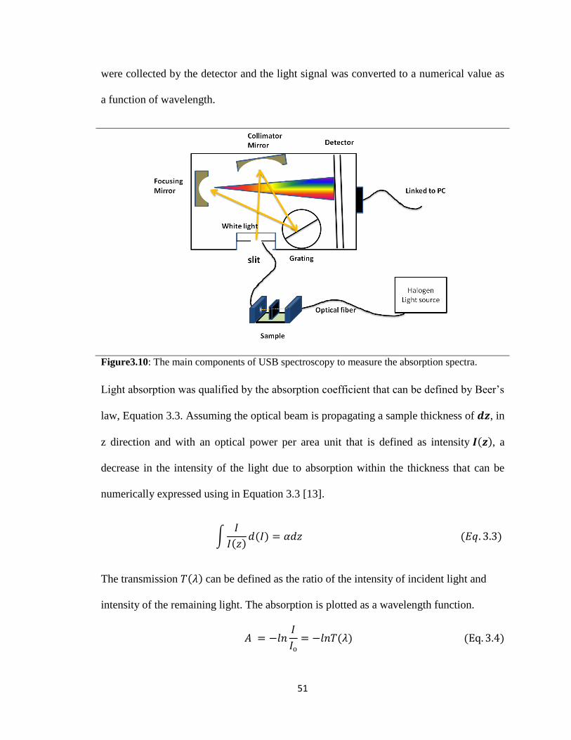
34 UV-Vis spectroscopy
Ultraviolet-visible absorption spectra of perovskite materials were obtained using an
Ocean Optics USB2000+ spectrometer and a DT-MINI-2-GS Deuterium-Halogen light
source As shown in Fig 310 light from deuterium halogen source travels through a
optical fibre Inside the spectrometer the amount of light is adjusted and the resolution
was controlled by the slit The directed light from the slit hits the collimator mirror that
focused the light onto an angled grating The main function of the grating is to split the
received light according to its wavelength and direct it to the focusing mirrors which
focus the first order spectra of the diffracted light onto the detector The spectra of light
Electron Gun
Anode
Condenser lens
Aperture
Sample
Vacuum pump
Backscattering Electron detector
SecondaryElectron detector
Scanning Coils
Sample
Chamber
Vacuum
Chamber
51
were collected by the detector and the light signal was converted to a numerical value as
a function of wavelength
Figure310 The main components of USB spectroscopy to measure the absorption spectra
Light absorption was qualified by the absorption coefficient that can be defined by Beerrsquos
law Equation 33 Assuming the optical beam is propagating a sample thickness of in
z direction and with an optical power per area unit that is defined as intensity a
decrease in the intensity of the light due to absorption within the thickness that can be
numerically expressed using in Equation 33 [13]
The transmission can be defined as the ratio of the intensity of incident light and
intensity of the remaining light The absorption is plotted as a wavelength function
52
Using the Tauc plot that governs the relation between the absorption coefficient α and the
incident photon energy the optical band gap can be determined [14 15] This relation
can be mathematically expressed as shown in Equation 35
That can be arranged to be in this well-known Tauc formula
Here is the optical band gap and parameter is constant related to the variation in
the semiconductor band and finally presents the order of the transition
Figure 311 Example of Tauc plot in red to determine the bandgap of semiconductor
Eg=149
53
35 References
1 Gao P M Gratzel and MK Nazeeruddin Organohalide lead perovskites for
photovoltaic applications Energy amp Environmental Science 2014 7(8) p 2448-
2463
2 Lv S S Pang Y Zhou NP Padture H Hu L Wang X Zhou H Zhu L
Zhang and C Huang One-step solution-processed formamidinium lead trihalide
(FAPbI(3minus x)Clx) for mesoscopic perovskitendashpolymer solar cells Physical
Chemistry Chemical Physics 2014 16(36) p 19206-19211
3 Park B-w B Philippe Tr ustafsson r Sveinbj rnsson A Hagfeldt EM
Johansson and G Boschloo Enhanced crystallinity in organicndashinorganic lead
halide perovskites on mesoporous TiO2 via disorderndashorder phase transition
Chemistry of Materials 2014 26(15) p 4466-4471
4 Yu H F Wang F Xie W Li J Chen and N Zhao The Role of Chlorine in the
Formation Process of ldquoCH3NH3PbI3‐xClxrdquo Perovskite Advanced Functional
Materials 2014 24(45) p 7102-7108
5 Boix PP K Nonomura N Mathews and SG Mhaisalkar Current progress
and future perspectives for organicinorganic perovskite solar cells Materials
Today 2014 17(1) p 16-23
6 Luo S and WA Daoud Recent progress in organic-inorganic halide perovskite
solar cells mechanisms and material design Journal of Materials Chemistry A
2015 3(17) p 8992-9010
7 Liang PW CY Liao CC Chueh F Zuo ST Williams XK Xin J Lin and
A Y Jen Additive enhanced crystallization of solution‐processed perovskite
54
for highly efficient planar‐heterojunction solar cells Advanced Materials 2014
26(22) p 3748-3754
8 Muumlller‐Buschbaum P The active layer morphology of organic solar cells probed
with grazing incidence scattering techniques Advanced Materials 2014 26(46)
p 7692-7709
9 Barrows AT S Lilliu AJ Pearson D Babonneau AD Dunbar and DG
Lidzey Monitoring the Formation of a CH3NH3PbI3ndashxClx Perovskite during
Thermal Annealing Using X‐Ray Scattering Advanced Functional Materials
2016 26(27) p 4934-4942
10 Kwak CK AT Barrows AJ Pearson DG Lidzey and AD Dunbar An X-
ray scattering and electron microscopy study of methylammonium bismuth
perovskites for solar cell applications Journal of Materials Research 2017 p 1-
11
11 Lilliu S T Agostinelli E Pires M Hampton J Nelson and JE Macdonald
Dynamics of crystallization and disorder during annealing of P3HTPCBM bulk
heterojunctions Macromolecules 2011 44(8) p 2725-2734
12 Kelsall R IW Hamley and M Geoghegan Nanoscale science and technology
2005 John Wiley amp Sons
13 Fox M Optical properties of solids 2002 AAPT
14 Aly K AA Elnaeim N Afify and A Abousehly Improvement of the electrical
properties of Se 3 Te 1 thin films by In additions Journal of Non-Crystalline
Solids 2012 358(20) p 2759-2763
55
15 Tauc J Amorphous and liquid semiconductors 2012 Springer Science amp
Business Media
56
Chapter 4 Dynamics of MAPbI3-xClx Perovskite Film
Crystallization
The aim of the chapter is to understand the dynamics of crystal formation MAPbI3-xClx
films The formation of crystals from the solution during spin coating and after thermal
annealing is studied using wide angle X-ray scattering in Sections 41 and 42 The
impact of thermal annealing on the morphology of the film is investigated by scanning
electron microscopy SEM in Section 43 The subsequent differences in the UV-Vis
spectra of the MAPbI3-xClx film and the extracted optical band gap are discussed in
Section 44 After the film is spin coated and annealed the storage conditions also need to
be considered Therefore the final part of the chapter will discuss the air exposure to the
annealed film in Section 45
41 In situ spin-coating of MAPbI3-xClx film
The crystallization mechanism of the most commonly used perovskite material in solar
cell applications MAPbI3-xClx was studies using wide angle X-ray scattering
The time dependent in situ spin-coating techniques of T-WAXS were used to probe the
early stages of the crystalline structure of the perovskite materials These early stages
observations at room temperature during the spin-coating we used assist to understand the
mechanisms of the intermediate phase before converting into the final perovskite phase
First the substrate mica was measured before perovskite deposition to identify which
WAXS features are associated with substrate and therefore can be ignored in our analysis
of the perovskite materials that are illustrated in Fig 41
57
The MAPbI3-xClx perovskite was prepared using a one-step technique After that it was
deposited on the mica substrate and using a vertical spin coater The solution coated the
film as was detailed in Chapter 3 in Section 32-1
Two spin coating speeds fast and slow were tested by setting the supply voltage for the
rotating motor to 20V that yields 3120 RPM or 10V that yields 1560 RPM respectively
The WAXS data collected at both spin-coating speeds are plotted in Fig 41 in
conjunction with the substrate data Significant substrate X-ray scattering peaks can be
observed at 14 Å-1
and at 216Å-1
and are labelled by () Scattering peaks related to
perovskite material on the surface of the mica can be distinguished at 085 Å-1
11 Å-1
and
12 Å-which were observed of both the fast and the slow spin-coating velocities
However the stronger intensity of WAXS and the additional scattering peaks can be
obtained from the slower speed The variation in spin-coating velocity directly affects the
thickness of the forming films Faster spin-coating leads materials distributed the edge of
the sample and a thinner film is formed Consequently additional scattering peaks and
the stronger WAXS intensity are obtained because of the thicker perovskite film forming
when we use the slower speed with a supply voltage of 10 V Subsequently all data of in-
situ WAXS experiments in this project are collected by the same speed at 1560 RPM
58
Figure 41 T-WAXS patterns of mica substrate before perovskite deposition shown as the red
line where the main scattering peaks are labelled () and the sample deposited at the slow speed
as the blue line and the sample deposited at the fast spin-coating speed as the black line
The scattering peak at q=11 Å-1
is generally assigned to the precursor phase of the
mixture of MAI and PbCl2 as was previously defined by wide angle X-ray scattering
studies [1 2] In both these previously published reports the scattering peaks at q=11 Å-1
were observed after the short thermal annealing time of 1 to 5 minutes The same peak
was detected and defined precisely as an intermediate product MAPbCl3 by Unger et al
[3] Chun-Yu Chang et al [4] and Hui Yu et al [5] in XRD measurements Their studies
highlighted strong diffraction peak at a Bragg diffraction angle of 157о which is the
converted to the scattering vector value of q=11 Å-1
using Eq 32 where the X-ray
wavelength is assumed to be λ=154 Å
As was proposed by Hui Yu et al the chemical reaction of 31 MAI with PbCl2 produces
several intermediate products involving two reaction steps [5] In the initial step PbI2
MAI and MACl react together to produce MAx+yPbI2+xCly Subsequently upon heating
59
the decomposition of intermediate product can yield the full perovskite phase as well as
MACl that is sublimated into gas The chemical reactions of 31 MAI with PbCl2 are
illustrated in Rect 41 and Rect 42
It was assumed for simplicity the MAx+yPbI2+xCly materials can be defined as MAPbCl3
[6]
Fig 42a shows the radial profiles of the in situ spin coating of T-WAXS for the MAPbI3-
xClx solution for duration of 10 minutes of processing times per second The T-WAXS is
referring to the transmission geometry of wide angle X-ray scattering
During the first minute the mica peaks at 14 Å-1and 216 Å
-1 were observed besides the
broad background scatter as expected from the solvent By increasing the processing
time a growth of crystallization of intermediate products was recognized A gradual
increase in WAXS intensity around q=11 Å-1
was detected that corresponded to the
intermediate phase of MAx+yPbI2+xCly The increase in the WAXS intensity at this
scattering vector was due to the rotating sample causing the solvent to dry by evaporation
after the initial liquid loss This results in forming a higher content of intermediate
product MAx+yPbI2+xCly during the spin-coating stage
In addition to the peak at q=11 Å-1
the weaker scattering of X-ray peaks recorded at
q=118 Å-1
q=16 Å-1
and q=2 Å-1
are assigned to the MAx+yPbI2+xCly intermediate phase
The positions of these scattering peaks are in agreement with experimental studies of the
60
X-ray diffraction analysis [7 8] and with the modelling work reported in [9] In these
reports the intermediate phase was described as an unstable cubic alpha phase With
emphasize that in this thesis we present the dynamic measurements during the spin
coating whereas in the previous studies the measurements were taken only at the end of
the casting processes
The X-ray scattering peaks between q=06 Å-1
to 08 Å-1
relate to the background scatting
from the solvent and the crystalline complex involving the solvent that was analyzed by
recent similar in-situ annealing X-ray scattering [10 6]
The features at q=062Å-1 q=14Å
-1 and around q=215Å
-1 are attributed to the content of
MAI in agreement the investigation of the crystal structure of MAI as reported
previously[11]
To visually present the degree of WAXS intensity during the WAXS exposure time a T-
WAXS intensity colour map is shown in Fig 42b Weaker WAXS intensity is
represented by different colour the stronger WAXS intensity is at the end of the
measurements This representation makes it easier to determine the intensity and ignoring
the background scattering from the solvent
Initially the highest intensity T-WAX area corresponds to the broad background
scattering band from 04 Å-1
to 08 Å-1
which dominates the first minute of deposition
times As the time increased the colour change from the dark red to the yellow and
eventually to light green indicates a changes in the WAXS intensity level that was
witnessed in the solvent evaporation and the forming of the crystalline film
61
The strong intermediate phase MAx+yPbI2+xCly intensity at 11 Å-1
that is associated with
the weaker T-WAXS intensity of the background scattering from the solvent that
becomes evident at t=100 s This indicates the rapid crystallization of MAx+yPbI2+xCly at
room temperature after the solvent evaporates After rapid initial growth the strong
intensity at q=11 Å-1
remains constant to the end of the T-WAXS measurement
The feature labelled by (♯) at 14 Å-1
is defined as the mica substrate with a combination
of the green line at 216 Å-1
that changes to the light blue line at the end of the T-WAXS
measurements The same features are attributed to the presence of MAI The X-ray
scattering area recorded at 17Å-1
is as attributed to the scattering signature of the
intermediate product MAx+yPbI2+xCly [12 4]
The changes in the width of important scattering peaks that refer to the intermediate
product MAx+yPbI2+xCly and MAI during the proceeding time were plotted and are shown
in Fig 43 The width of the WAXS peaks gives an estimated value of the crystal size
The wider the peaks the smaller the size of the crystals[13] In the measurements
presented the crystal size of the MAI and MAx+yPbI2+xCly was changed inversely as
indicated by the change in FWHM The crystal size of the MAI started smaller and after
200s changes to bigger size which indicate converted into MAx+yPbI2+xCly The bigger
MAI crystals can also be attributed to MAI impurity After 250s the crystal size of MAI
and MAx+yPbI2+xCly remains unchanged This indicates that the conversion processes
between the MAI and MAx+yPbI2+xCly occur fast during the first 3 minutes
The dynamic formation of MAPbI3-xClx perovskite film during the spin coating data
suggested that two stages of crystal formation The plot of the scattering intensity of the
62
main features related to the solvent at the centre at q=055 Å-1
intermediate product
MAx+yPbI2+xCly at q=11 Å-1
and the scattering of MAI and mica at 14 Å-1
as a function
of the time is shown in Fig 44 The first stage is the solvent loss during the first min
whereas after that the crystallisation stage of the intermediate product MAx+yPbI2+xCly is
occurred
63
Figure 42 Summary of 1D of line profiles of T-WAXS of MAPbI3-xClx precursor recorded
during spin coating (a) T-WAXS profiles as a function of exposure time of X-ray (b) The
growth evolution of the precursor during 10 min presented in a contour plot of T-WAXS
intensity
(a)
(b)
64
Figure 43 The change in FWHM of the scatterings peaks at MAI and intermediate product
MAx+yPbI2+xCly during the processing time of in situ spin coating
Figure 44 Intensity of the main features of T-WAXS of MAPbI3-xClx perovskite film as a
function of the time
65
Fig 45 displays 2D WAXS image of the MAPbI3-xClx film that was taken once the
spinning had stopped Some X-ray scattering spots are arranged in rings that are observed
in the area between q=06 Å-1
and q=11 Å-1
The multiple scattering spots observed are distributed along rings The spots are caused
by X-ray scatting from several individual crystallites at 11Å-1
at (100) after solvent
evaporation If enough individual crystallites are present a continuous ring would be
observed as occurs in a powder diffraction experiment In Fig 45 the spots are not
preferentially distributed in any particular section of the ring There is an equal spread
around the out of plane direction the in plane direction and all angular directions in
between indicating random orientation of crystallites present As was explained in
Chapter 3 the full ring indicates that the crystals are orientated in random directions
including vertical and horizontal or angular directions Based on the direction of the
orientation the combinations of X-ray group scattering signals are arranged to form
scattering rings The room temperature observation presented here is in agreement with
the initial observations made in a recent in situ grazing incidence WAXS study where
the perovskite films were first deposited by spray coating and then dynamics
measurements were taken during the annealing process [14] Here we observed that the
high order intermediate crystallites can be formed with random orientations without any
heat assistance The X-ray scattering of completed perovskite phase therefore can be
seen if the substrates or the perovskite ink are preheating as was observed in [10 14]
66
Figure 45 2D T-WAXS patterns of MAPbI3-xClx ink after the spin coating
42 Crystalline Structure of Annealed MAPbI3-xClx Film Investigated by
WAXS
In Section 41 it was shown that solvent evaporation assists the crystallization and
formation of the intermediate product MAx+yPbI2+xCly which resulted in a WAXS signal
detected at q=11 Å-1
This unstable cubic structure of the intermediate phase was
observed during the dynamic spin coating process at room temperature In this section
the role of the high (90оC) temperature in forming the full perovskite phase will be
explored Perovskite ink from the MAI and PbCl2 prepared in the same method as
described in Section 32-1 and was deposited on mica substrates and after spin coating
the sample moved into a hot plate then was annealed at 90о
C for 2 hours and measured
using WAXS techniques
Fig 46 compares the one-dimensional T-WAXS pattern of the dry film formed after spin
coating and the T-WAXS pattern of the annealed film The scattering peak correspond
67
into the as cast intermediate perovskite structure that was detected at 11 Å-1
mostly
disappears after annealing the film This indicates instability of the intermediate
perovskite structure that forms during the spin coating processes
On the other hand the scattering peaks are clearly visible at q=1 Å-1
and 2 Å-1
and did not
exist after the spin coating processes As in the previous section features at scattering
vectors q = 14 Å-1
and 216 Å-1
correspond to scattering from the mica substrate and MAI
that are labelled () were observed
The peaks at q=1Å-1
and 2Å-1
are assigned to the (110) and (220) crystal planes of the
tetragonal structure in the complete MAPbI3-xClx perovskite phase Similar peaks have
previously been observed at 2 = 141о and 2842
о which using Eq 32 converted to q
values of 1 Å-1
and 2 Å-1
as was reported in the wide angle X-ray scattering studies in
the literature [15-17]
The changes observed during annealing the perovskite are attributed to a phase change
occurring during thermal annealing This process indicates a complete chemical reaction
as was explained in Rect 42 through a conversion from the intermediate cubic structure
to a more stable tetragonal structure
In the 1D T-WAXS spectra of the annealed perovskite film shown in Fig 46 weak
scattering peak at q=1 Å-1
and some weak evidence of the intermediate scattering peak
remaining at q=11 Å-1
were observed which indicates the existence of a small amount of
residual intermediate product and some of the precursor materials that contribute to the
impurity of the perovskite films
68
Fig 47 illustrates a full scattering ring at q=1 Å-1
The full rings of the X-ray scattering
are apparent due to probing many smaller crystals with more random orientations so
probing more orientations of crystal planes as was illustrated in Fig 32 [18] The SEM
data are confirmed this in next section
Based on this concept the annealed MAPbI3-xClx film can be described as thicker films
with randomly orientated crystals at q=1 Å-1
In contrast only some degree of orientation
presented lower content of materials can be extracted from the 2D WAXS data from the
dry film that formed before the thermal annealing as seen in Fig 47 The observation of
random orientations of the MAPbI3-xClx annealed film is similar to what was highlighted
previously [10 14 16]
Figure 46 Comparison between the T-WAXS patterns of MAPbI3-xClx after spin coating and
after thermal annealing
69
Figure 47 2D T-WAXS data of MAPbI3-xClx recorded (a) before and (b) after the thermal
annealing
43 Morphological Study of MAPbI3-xClx Film
Scanning electron microscopy (SEM) was used to conduct a morphological study of the
MAPbI3-xClx perovskite film to further explore the effects of the thermal annealing The
surfaces of the MAPbI3-xClx perovskite films before and after the thermal annealing for
different annealing times were studied Fig 48 shows images of the surface of the
MAPbI3-xClx perovskite film as a function of the annealing time in the range of 0ndash120
min (at 90о C)
Before thermal annealing (Fig 48a) the surface appears cross shape crystals that most
likely corresponding to the intermediate perovskite MAx+yPbI2+xCly After heating the
film at 90оC for half an hour (Fig 48b) there is a subtle morphological change the large
cross shape crystals turn into a single continuous film
As the annealing time increases from 30 min to 60 min (Fig 48c) the surface coverage
of the film is more complete and the gaps between the crystals domains are further
70
reduced The increase in the film coverage and reduction in the pinhole with the increase
of film heating time is attributed to evaporating the MACl product into a gas and the
initial formation of the final perovskite phase MAPbI3 In other words the chemical
reaction of MAI and PbCl2 is completed after 60 min of annealing as was proposed [5]
An increase in surface coverage can be seen clearly after 2 hours of annealing (Fig 48d)
which is the recommended annealing time to form a perovskite film in air [19 20] The
existence of a few pin holes at this annealing time is possibly due to the continued
presence of a low content of un-reacted amorphous material or the intermediate phase
MAx+yPbI2+xCly which was not fully converted into the final perovskite phase thus
yielding a slightly impure film containing un-reacted materials as was also indicated in
the 1D-WAXS data in Fig 4 6
71
Figure 47 (a) Surface morphology of MAPbI3-xClx observed by SEM directly after spin coating
(b) annealed film for 30 min (c) 60 min and (d) 120 min
a) 0min b) 30min
c) 60min d)120min
72
44 UV-Vis spectra of MAPbI3-xClx Film
The optoelectronic behavior of the MAPb3-xClx films was investigated by measuring their
absorption spectra using a UV-Vis spectrometer The inks containing MAI and PbCl2
were prepared as described in Section 31-1 The ink was then deposited onto glass
substrates Three of the samples were heated to 90о
C for 30 min 60 min and 120 min
respectively whereas the fourth sample was measured as cast without any annealing
The results of the light absorption spectra for the four MAPb3-xClx samples are presented
in Fig 49(a-d) Samples (a-c) exhibit different gradients in the spectra over the visible
and near IR ranges between 750 nm to 800 nm In contrast an almost flat absorbance line
was observed in the film without any annealing in sample (d) This behaviour of the light
absorption spectra is similar to what was reported from MAPbI3-xClx previously [21 22]
The light absorption spectra are also in the agreement with what was observed in the
MAPI3 perovskite film [23 24]
The absence of the absorption edge in the perovskite sample that was prepared without
annealing is due to the absence of the final perovskite crystalline phase at this stage The
surface coverage and T-WAXS data of the film as cast presented separated crystals of
intermediate product MAx+yPbI2+xCly as identified in Fig 48 and Fig 42
The poor solar light absorption at these materials that would mean a lower PCE for solar
cell devices made without thermal annealing
The optical band gap for the material in the film annealed for 2 hours at 90о
C was
calculated from the UV-Vis spectra by fitting a straight line to a Tauc plot and was found
to be 155 eV (Fig 49) This optical band gap for the MAPbI3-XClX perovskite
73
semiconductor is in the range of the theoretical optimum band gap of solar cell devices
that can deliver a current density of 27 mAcm2 as was discussed in Chapter 2 [25 26]
Figure 49 UV-Vis spectra of MAPb3-xClx perovskite annealed for (a) 2 hours (b) 60 min (c)
30 min (d) annealed film and the extracted band gap in the Tauc plot
45 Air exposure effects on Annealed Film
After a perovskite ink is prepared and deposited onto the substrate and spin coated to
form a film that is subsequently thermally annealed it should be storedused in such a
74
way as to prevent any damage The storage conditions of perovskite as a film or as a
photoactive layer within solar cell devices are crucial factors in determining the lifetime
of perovskite solar cells
Encapsulation is the most common way to protect the perovskite film in a solar cell to
slow down its degradation An undesirable short lifetime of the MAPbI3-xClx perovskite
materials has been reported [27 28] This short lifetime results from degradation of the
perovskite into other chemical materials in the presence of oxygen and high humidity
(more than 60) [29]
To investigate the effect of air exposure on the crystal structure of the annealed MAPbI3-
xClx perovskite film WAXS characterisation was used The WAXS ring of the film
before and after air exposure was obtained and is illustrated in Fig 410b c The
perovskite WAXS ring shows bright scattering ring of a full completed phase of MAPbI3-
xClx at q=1 Å-1
after air exposure which indicated the material degradation This
degradation can be better observed by WAXS scattering before 075Å-1
which is related
to the precursor materials However 2D WAXS data reveals the slight appearance of a
visual ring at q=09 Å-1
that corresponds to PbI2
Fig 410 shows the WAXS profiles of the MAPbI3-xClx film stored in an evacuated
dissector and of another nominally identical film that was exposed to air for
approximately 5 hours Radial sector integration profiles from the 2D T-WAXS
scattering patterns from the MAPbI3-xClx film after air exposure shows a relatively
weaker peak intensity at the original final perovskite features associated with scattering
from(110) and (220) planes at q=1 Å-1
and q=2 Å-1
respectively (Fig 410) Moreover
75
new features in the WAXS profiles appear as peaks at q=045 Å-1
q=07 Å-1
and q=09 Å-
1 The pre-annealing intermediate phase that is characterized by a peak at 11Å
-1 can be
seen to have reappeared (Fig 410)
The reduction of WAXS intensity at q=1 Å-1
after air exposure originates from the loss
of the MAPbI3-xClx material which may decompose into PbI2 that is responsible for
showing the WAXS peak at q=09 Å-1
as was defined previously [30] The existence of
some peaks related to the MAI content at q=045 Å-1
and q=07 Å-1
indicates the reverse
direction of the chemical reaction between MAI and PbCl2 in the presence of air
76
Figure 410 profiles of T-WAXS of annealed MAPbI3-xClx film stored in a vacuum and in the air
(a) and 2D WAXS of the same films that are stored in a (b) vacuum and in the air (c)
To better understand the change in the crystal structure of MAPbI3-xClx film after air
exposure these observations in the crystalline structure of the MAPbI3-xClx that was
prepared under ambient conditions suggest that the MAPbI3-xClx film should be stored
under vacuum conditions to prevent any rapid degradation
(a)
77
46 Summary
In this chapter perovskite materials prepared by mixing MAI and PbCl2 in a 31 molar
ratio and dissolved in a DMF solvent were investigated
The final perovskite phase desirable for solar cell applications was achieved after
annealing at 90о
C Forming this phase that was observed by X-ray scatter at the (110)
and (220) and crystal formed slowly Therefore a longer time for annealing was required
exceeding 2 hours Annealing for a longer time can also assist in forming better coverage
and fewer pinholes that are reflected in the performance of perovskite solar devices In
terms of solar light absorption an enhancement was observed in the UV-Vis spectra
resulting from the complete reaction after annealing the film for 2 hours
This chapter also discusses the impact of the storage method of the film on the crystal
structure of MAPbI3-xClx and its orientation The remarkable degradation into the
precursor materials was observed in the film that was stored in humid air for 5 hours and
a change in the crystal orientation was observed as well Therefore after preparing the
MAPbI3-xClx materials in air the material should be stored under vacuum conditions or at
least with minimal exposure time to the air to guarantee a prolonged lifetime of the
MAPbI3-xClx films which will enhance the lifetime of perovskite solar cell devices
47 References
1 Huang Y-C C-S Tsao Y-J Cho K-C Chen K-M Chiang S-Y Hsiao C-
W Chen C-J Su U-S Jeng and H-W Lin Insight into Evolution Processing
and Performance of Multi-length-scale Structures in Planar Heterojunction
Perovskite Solar Cells Scientific reports 2015 5 p 13657
78
2 Tan KW DT Moore M Saliba H Sai LA Estroff T Hanrath HJ Snaith
and U Wiesner Thermally induced structural evolution and performance of
mesoporous block copolymer-directed alumina perovskite solar cells Acs Nano
2014
3 Unger EL AR Bowring CJ Tassone VL Pool A Gold-Parker R
Cheacharoen KH Stone ET Hoke MF Toney and MD McGehee Chloride
in lead chloride-derived organo-metal halides for perovskite-absorber solar cells
Chemistry of Materials 2014 26(24) p 7158-7165
4 Zhou H Q Chen G Li S Luo T-b Song H-S Duan Z Hong J You Y
Liu and Y Yang Interface engineering of highly efficient perovskite solar cells
Science 2014 345(6196) p 542-546
5 Yu H F Wang F Xie W Li J Chen and N Zhao The Role of Chlorine in the
Formation Process of ldquoCH3NH3PbI3‐xClxrdquo Perovskite Advanced Functional
Materials 2014 24(45) p 7102-7108
6 Chang C-Y Y-C Huang C-S Tsao and W-F Su Formation Mechanism and
Control of Perovskite Films from Solution to Crystalline Phase Studied by in Situ
Synchrotron Scattering ACS applied materials amp interfaces 2016 8(40) p
26712-26721
7 Colella S E Mosconi P Fedeli A Listorti A Rizzo F Gazza F Orlandi P
Ferro T Besagni and G Calestani MAPbI 3-x Cl x mixed halide perovskite for
hybrid solar cells the role of chloride as dopant on the transport and structural
properties MRS Online Proceedings Library Archive 2014 1667
79
8 Poglitsch A and D Weber Dynamic disorder in
methylammoniumtrihalogenoplumbates (II) observed by millimeter‐wave
spectroscopy The Journal of chemical physics 1987 87(11) p 6373-6378
9 Mosconi E A Amat MK Nazeeruddin M Graumltzel and F De Angelis First-
Principles Modeling of Mixed Halide Organometal Perovskites for Photovoltaic
Applications The Journal of Physical Chemistry C 2013 117(27) p 13902-
13913
10 Barrows AT S Lilliu AJ Pearson D Babonneau AD Dunbar and DG
Lidzey Monitoring the Formation of a CH3NH3PbI3ndashxClx Perovskite during
Thermal Annealing Using X‐Ray Scattering Advanced Functional Materials
2016 26(27) p 4934-4942
11 Jeon NJ JH Noh YC Kim WS Yang S Ryu and SI Seok Solvent
engineering for high-performance inorganicndashorganic hybrid perovskite solar cells
Nature materials 2014 13(9) p 897-903
12 Liu J C Gao X He Q Ye L Ouyang D Zhuang C Liao J Mei and W
Lau Improved crystallization of perovskite films by optimized solvent annealing
for high efficiency solar cell ACS applied materials amp interfaces 2015 7(43) p
24008-24015
13 Scherrer P Estimation of the size and internal structure of colloidal particles by
means of roumlntgen Nachr Ges Wiss Goumlttingen 1918 2 p 96-100
14 Lilliu S J Griffin A Barrows M Alsari B Curzadd T Dane O Bikondoa
JE Macdonald and D Lidzey Grain rotation and lattice deformation during
80
perovskite spray coating and annealing probed in situ by GI-WAXS
CrystEngComm 2016 18(29) p 5448-5455
15 Liu M MB Johnston and HJ Snaith Efficient planar heterojunction
perovskite solar cells by vapour deposition Nature 2013 501(7467) p 395-398
16 Miyadera T Y Shibata T Koganezawa TN Murakami T Sugita N
Tanigaki and M Chikamatsu Crystallization Dynamics of Organolead Halide
Perovskite by Real-Time X-ray Diffraction Nano letters 2015 15(8) p 5630-
5634
17 Wang ZK M Li YG Yang Y Hu H Ma XY Gao and LS Liao High
Efficiency PbndashIn Binary Metal Perovskite Solar Cells Advanced Materials 2016
28(31) p 6695-6703
18 Muumlller‐Buschbaum P The active layer morphology of organic solar cells probed
with grazing incidence scattering techniques Advanced Materials 2014 26(46)
p 7692-7709
19 Ahmadian-Yazdi MR F Zabihi M Habibi and M Eslamian Effects of
Process Parameters on the Characteristics of Mixed-Halide Perovskite Solar Cells
Fabricated by One-Step and Two-Step Sequential Coating Nanoscale Research
Letters 2016 11(1) p 408
20 Kim JH ST Williams N Cho CC Chueh and AKY Jen Enhanced
Environmental Stability of Planar Heterojunction Perovskite Solar Cells Based on
Blade‐Coating Advanced Energy Materials 2015 5(4)
81
21 Dinnocenzo V G Grancini MJ Alcocer ARS Kandada SD Stranks MM
Lee G Lanzani HJ Snaith and A Petrozza Excitons versus free charges in
organo-lead tri-halide perovskites Nature communications 2014 5 p 3586
22 Lee MM J Teuscher T Miyasaka TN Murakami and HJ Snaith Efficient
Hybrid Solar Cells Based on Meso-Superstructured Organometal Halide
Perovskites Science 2012 338(6107) p 643-647
23 Kazim S MK Nazeeruddin M Graumltzel and S Ahmad Perovskite as light
harvester a game changer in photovoltaics Angewandte Chemie International
Edition 2014 53(11) p 2812-2824
24 Sakai N S Pathak H-W Chen AA Haghighirad SD Stranks T Miyasaka
and HJ Snaith The mechanism of toluene-assisted crystallization of organicndash
inorganic perovskites for highly efficient solar cells Journal of Materials
Chemistry A 2016 4(12) p 4464-4471
25 Green MA A Ho-Baillie and HJ Snaith The emergence of perovskite solar
cells Nature Photonics 2014 8(7) p 506-514
26 Shockley W and HJ Queisser Detailed balance limit of efficiency of p‐n
junction solar cells Journal of applied physics 1961 32(3) p 510-519
27 Luo S and WA Daoud Recent progress in organic-inorganic halide perovskite
solar cells mechanisms and material design Journal of Materials Chemistry A
2015 3(17) p 8992-9010
28 Niu G X Guo and L Wang Review of recent progress in chemical stability of
perovskite solar cells Journal of Materials Chemistry A 2015 3(17) p 8970-
8980
82
29 Niu G W Li F Meng L Wang H Dong and Y Qiu Study on the stability of
CH 3 NH 3 PbI 3 films and the effect of post-modification by aluminum oxide in
all-solid-state hybrid solar cells Journal of Materials Chemistry A 2014 2(3) p
705-710
30 Guo X C McCleese C Kolodziej AC Samia Y Zhao and C Burda
Identification and characterization of the intermediate phase in hybrid organicndash
inorganic MAPbI 3 perovskite Dalton Transactions 2016 45(9) p 3806-3813
83
Chapter 5 The Dynamics of FAPbI3-xClx Perovskite Films
Crystallization
In the previous chapter the crystal structure of the most widely used perovskite material
MAPbI3-xClx was investigated during in situ spin coating by T-WAXS and ex situ after
thermal annealing Using the same technique FAPbI3-xClx perovskite film will be
investigated in this chapter
The results of the T-WAXS collected during spin coating are detailed in Section 51 In
Section 52-1 the effects of different annealing temperatures and times on the quality of
crystalline film FAPbI3-xClx will be demonstrated The morphology study of these
different annealing conditions of FAPbI3-xClx films will be illustrated in Section 52-2
The main difference between T-WAXS features of the annealed film and the just coated
film is highlighted in Section 52-3 Measurement of changes to the T-WAXS profiles for
a long time (9h) after deposition is explored to study the degradation of FAPbI3-xClx
perovskite film in Section 524
Measurements of UV-Vis spectra and the optical band gap are discussed in Section 53
Finally the main findings will be highlighted in the chapterrsquos conclusion in Section 54
51 T-WAXS experiments during in-situ spin coating of the solution to
produce FAPbI3-xClx perovskite films
The perovskite ink prepared by mixing FAI and lead chloride as described in Chapter 3
in Section 31 was investigated during spin coating to understand the formation
mechanisms of the crystalline products Fig 51 presents the T-WAXS data of the
84
solutions used to produce perovskite during the first ten minutes of the spin casting
process Fig 51(a) shows the time dependent measurement of T-WAXS radial profiles of
perovskite ink During the first six minutes of the T-WAXS collection The broad solvent
related feature is present initially and slowly disappears and the dominant feature that can
be detected is a peak around q=14 Å-1
This T-WAXS peak as was discussed in Chapter
4 is attributed to scattering from the mica substrates on which the perovskite inks were
deposited As the processing time increased some features eventually form in the T-
WAXS profiles at 330 s indicating the initial stage of formation of the intermediate
products of FAPbI3-xClx
T-WAXS peaks at q=14 Å-1
is also attributed the present of PbCl2 in agreement with the
XRD data of the individual measurements of PbCl2 [1 2] The clear and gradual
enhancement in the T-WAXS intensity of X-ray scattering signals at 07 Å -1
and 11 Å -1
and several other weak peaks over time indicates that these peaks are related to materials
that crystalize on the surface of the substrate as the solvent evaporates over time
The T-WAXS peaks at 07 Å -1 13 Å
-1 16 Å
-1 18 Å
-1and 23 Å
-1are attributed to the
presence of the hexagonal structure of yellow-perovskite phase of δ-FAPbI3 as was
reported in X-ray diffraction results using a Cu α X-ray radiation source with λ=154 Å
in [2 3]
The T-WAXS signal at 11 Å-1
is equivalent to the X-ray diffraction angle of 153о (for
Cu Kα) that was reported and is attributed to FACl[4] Therefore the X-ray scattering
peak at 11 Å -1
is defined as scattering caused by the intermediate product FACl
85
To determine the formation time and the degree of T-WAXS intensity of each phase or
product the colour intensity map plot of T-WAXS profiles of perovskite ink during the
spin coating is provided in Fig51 (b) A higher intensity degree of X-ray scattering is
represented early at 330 s at q=07 Å-1
where the slower crystallization of FACl is
represented by the weaker line at q=11 Å-1
The intensity map of T-WAXS profiles of perovskite ink drying shows several features of
X-ray scattering and the lines may be divided into different materials The first area
shows a noticeable background X-ray scattering detected between 04 Å-1
and08 Å-
1which is attributed to the background scattering from the solvent within the mixture of
PbCl2 and FAI This area exhibits a gradual decrease in the T-WAXS intensity during the
spin coating time and was less pronounced after t=330 s when the solvent will have
nearly finished evaporating
As the exposure time of T-WAXS increased after 330 s the yellow FAPbI3 phase
formed as revealed by the dark red line and labelled by (δ) centred at q=07 Å-1
The
weaker X-ray scattering detected at 13 Å-1
16 Å-1
18 Å-1
and 23 Å-1
are also attributed
to δ-FAPbI3 [5]
The intermediate phase labelled by (diams) is associated with FACl as was reported before
[4] This intermediate product is defined by strong X-ray scattering but not as strong as
the yellow phase δ-FAPbI3 A slower crystallization mechanism for FACl as compared to
δ-FAPbI3 is observed it took 420 s for it to appear compared to 330 s
86
At the end of the drying time of solvent the initial stage of perovskite phase of FAPbI3-
xClx are detected at q=1 Å-1
and q=2 Å-1
These features agreed with the values for Bragg
diffraction angle of 145о and 28
о previously
reported [4 2]
A summary of the most important T-WAXS features during the spin coating and the
appearancersquos times are provided in Table 51
In Fig 52 the FMHW of the X-ray scattering peaks that are defined in Fig 51 is plotted
as a function of the time The crystals start to grow after 250s which is the slower
crystallisation compared to perovskite ink containing MAI and PbCl2 Wider peaks of the
complete perovskite crystal mean a smaller size compared to the discontinuous phase and
hexagonal yellow perovskite crystals In contrast the intermediate perovskite including
FACl and δ-FAPbI3 records larger size Despite that direct growth of the FAPbI3 crystal
at the spin coating the larger intermediate crystals are not decomposed This could
indicate the need for the high temperature to complete the chemical reaction to produce
the larger perovskite crystals and decompose the larger intermediate crystals
Overall based on the in situ T-WAXS profiles collected during the spin coating and
crystallization of the perovskite ink containing FAI and PbCl2 can be divided into three
stages The first stage involves background scattering of the solvent with the mixture of
PbCl2 and FAI that is lost gradually The next stage of crystallization is associated with
the dry film and is dominated primarily by yellow phase δ-FAPbI3 forming at 330 s The
intermediate product of FACl appears in the third stage after 420 s Simultaneously the
forming of a lower content (compared to the δ-FAPbI3) of tetragonal perovskite crystals
at q=1Å is noted The three stage of crystals formation are illustrated in Fig 53 where
87
the intensity of these scattering products is plotted against the processing time The
converting from the intermediate phase FACl to the perovskite phase FAPbI3-xClx is
defined between 420 s and 440 s
The direct forming of FAPbI3-xClx perovskite phase during the spin coating is the
distinguishing feature in this measurement whereas in the observation of in situ spin
coating of MAPbI3-xClx film only crystals of intermediate products were formed
indicated two stages of crystal formations
88
Figure 51 Summary of profiles of T-WAXS of FAPbI3-xClx precursor recorded during spin
coating (a) T-WAXS profiles as a function of processing time (b) The growth evolution of the
precursor over duration of 10 min presented in colour map of T-WAXS intensity
(a)
(b)
89
Figure 52 Variation in FWHM of intermediate phase δ-FAPbI3 FACl at q=11Å-1
peaks and the
scattering peak of perovskite crystal at FAPbI3-xClx as a function of the time
Presented
Materials
X-ray scattering vectors
(Å-1
)
Forming Time (s)
Solvent+(PbCl2
+FAI)
06 From t=0 to t=330
δndashFAPbI3 07 13161823 From 330s to the end
FACl 11 After 420s
FAPbI3-xClx
10 After420s
Table53 Summary of the X-ray scattering areas and the estimated starting time for formation
during the spin coating of perovskite ink of (DMF solvent with PbCl2+FAI)
90
Figure 53 Intensity of the solvent background scattering at q=06 Å
-1 the δ-phase at q=07Å
-1
intermediate product of FACl at q=11 Å-1
and perovskite phase FAPbI3-xClx at 1 Å-1
with sketch
illustrate the forming stages
52The Effects of Thermal Annealing on Crystallization of FAPbI3-xClx
Perovskite films
Several X-ray scatting peaks were observed during spin coating that are associated with
the yellow perovskite δ-FAPbI3 with hexagonal structure the chloride doping owing to
the presence of FACl and lower content of FAPbI3-xClx perovskite crystals that all
appeared before any annealing The next section will discuss the crystalline structure of
perovskite after thermal annealing
52-1 Thermal Annealing Conditions of FAPbI3-xClx Film
The effects of different annealing temperatures and times on the crystalline structure of
FAPbI3-xClx film were investigated by grazing incidence wide angle X-ray scattering GI-
WAXS The geometry of the X-ray scattering experiments used here are quite different to
the T-WAXS experiments already presented in Chapter3 further details are available in
Tim
e(s
)
δ-FAPbI3
FACl
FAPbI3-xClx
33
0420
Solution
60
00
91
the methods Section 33-2 Samples of FAPbI3-xClx were spin coated and annealed inside
a nitrogen filled glove box to minimize affects of moisture and humidity exposure The
most crucial difference in the GI-WAXS experiment is the ability to use very small
incident X-ray angles that detect only the surface of the film Therefore transparent
substrates are not long required in this work Si substrates (with a native oxide) were
used As was detailed in the experimental methods in Chapter 3 the ranges of the
incident angles (αi) used were from 01о to 06
о with a step size of 002
о
The intensity of the collected X-ray signals varied based on the incident angles (αi) In
order to evaluate the angle used to detect the higher intensity signals that is called the
critical angle we plotted the intensity of the significant features at q=1 Å-1
and q=2 Å-1
of
the film against the incident angles (αi) in Fig 54 The maximum intensity collected at
αi=026о and this curve is similar to what was reported before in GI-WAXS experiments
[6 7] However there are some similar features at 15о
and near 3о that are likely due to
the roughness of the surface The surface of the FAPbI3-xClx perovskite films is not flat as
is illustrated by the SEM measurements in the next section This roughness makes it
difficult to define the precise grazing incidence angle in the GI-WAXS experiments Fig
55 compares an ideal flat sample and our perovskite sample However the maximum
intensity collected was on average at 026о which was defined as the critical angle GI-
WAXS data collected at angles below this angle are assumed to be mostly from the
higher layer of the surface where most of the beam is reflected Above this angle the
beam propagates the whole depth of the film
GIWAXS profiles at X-ray incident angle of 026о for the FAPbI3-xClx films annealed at
130оC 170C and 190
оC and one without annealing are plotted in Fig 56 for
92
comparison The sample annealed at 130оC has similar features as the sample that was
not annealed but with lower scattering intensity The extra peak shown Fig 56(b) at q
09 Å-1
is most likely due to the presence of PbI2 [2] This feature is implying the initial
thermal stage needs to intermediate forming to the final stage of perovskite phase
Fig 56 (a) and (b) provide profiles that are mostly defined by presence of the yellow
phase of δ-FAPbI3 at scattering vectors 07 Å-1 13 Å
-1 15 Å
-1 18 Å
-1 23 Å
-1
The
intermediate products FACl at scattering vectors 11 Å-1
and 22 Å-1
and this was also
confirmed by room temperature in-situ T-WAXS data as shown in Fig 51 However the
higher intensity of FACl indicates the higher content of FACl that observed in Fig 56
could depend on the sample preparation conditions
Fig 56(c d) shows the GI-WAXS profiles related to higher temperature annealing at
170оC and 190
оC degrees at which the film is distinguished by the preferable complete
perovskite phase having scattering peaks at q=10 Å-1
and q=20 Å-1
This indicates the
need of an annealing temperature higher than 130оC to form the desired tetragonal
crystalline structure of perovskite Despite the similarity in GI-WAXS profiles in
Fig55(c d) some weaker GI-WAXS peaks observed at 09 Å-1
that could originate from
the PbI2 or δ-FAPbI3 These completely disappear at 190оC
All the characterised FAPbI3-xClx films in Fig 55 were annealed for 30 minutes Longer
or shorter annealing times could make a difference in film formation so to further
investigate the significance of different annealing times we annealed films of FAPbI3-xClx
to 170оC for 15 30 and 60 min The GI-WAXS profiles of these films and an un-
annealed sample profile are presented in Fig 56
93
After annealing for only 15 minutes the X-ray scattering pattern of the FAPbI3-xClx film
changes Clearly this time was sufficient to remove the thermally decompose the FACl
as indicated by the absence of the scattering peaks at 11 Å-1
and 22 Å-1
in Fig 56 (b)
The visible weak scattering signals recorded at 099Å-1
and 20Å-1
indicates the initial
forming stage of tetragonal perovskite FAPbI3-xClx crystals In connection with T-WAXS
data shown in Fig 51 at room temperature for ten minutes processing time we can
observe the fast crystallisation of the perovskite phase of FAPbI3-xClx Beside the weaker
feature that relates to the perovskite phase there is also peaks at086 Å-1
and 19 Å-1
that
is most likely are most attributed to the lead existence in the sample
The longer annealing times of 30 and 60 min enhance the perovskite crystallisation
leading to X-ray scattering at q=10 Å-1
and q=20 Å-1
as is illustrated in Fig 57(cd)
Figure 54 The intensity of the perovskite related features in the GI-WAXS data at q=1Å-1
and
q=2Å-1
plotted as a function of the grazing incidence angle The maxima intensity reflected of GI-
WAXS at 026ordm
94
Figure 55 The effect the roughness of the film surface on the WAXS intensity where the
directions of the reflected beam can be seen in the rough sample
Figure 56 GI-WAXS patterns of FAPbI3-xClX perovskite prepared at room temperature RT (a)
and annealed at 130оC (b) 170
оC (c) and 190
оC (d)
WAXS incident Reflection WAXS incident
Reflection
Substrate
Surface of the film
95
Figure 57 GI-WAXS patterns of FAPbI3-xClX perovskite without annealing (a) and annealed at
170оC for 15min (b) 30min (c) and 60min (d)
52-2- Investigation of Surface Morphology of FAPbI3-xClx
The film of FAPbI3-xClx perovskite before and after the thermal annealing was
investigated by SEM to study the effects of the heat on the surface coverage Fig 58
compares the SEM images of the surfaces of the FAPbI3-xClx films Before annealing the
SEM image features clearly crystalline grains most of which have an approximately
hexagonal shape embedded within a more homogeneous material
In contrast the surface coverage has significantly increased after annealing at 190оC for
30 min The hexagonal grains have disappeared which might indicate that the grains
have decomposed completely The morphology of the FAPbI3-xClx film is further affected
by the annealing times which indicate the homogeneous materials eventually acquired
some texture This is indicating that there may be crystalline materials embedded within
it as also indicated by GI-WAXS data results in Fig 57
96
The surface of FAPbI3-xClx film annealed at 190оC at different annealing times (15 30
and 60 min) is shown in Fig 59 (a b c) The remarkable increase in the coverage of the
filmrsquos surface was observed with increase annealing time which indicates the need to
anneal for more than 15 min to form a smaller number of pinhole-sized pores in the film
which is desirable for high efficiency photovoltaic devices This fact is corroborated by
the GI-WAXS data shown in Fig 57 where the lower TWAXS signals indicate poor
morphology at shorter annealing time (15 minutes) The surface converge calculated at
15 min annealing is 50 whereas is 85 when the annealing time doubled and the best
converge is 94 after 60 minutes of annealing
Figure 58 The surface of the solution is containing FAI PbCl2 and DMF solvent after spin
coating forming a wet film the grains illustrate the hexagonal geometry and the film after the
thermal annealing is shown in (b)
97
Figure 59 The surface of the annealed film to 170 degC for a) 15min b) 30min and c) 60 min
52-3 Changes in Perovskite Crystalline Structure of FAPbI3-xClx Film After
Thermal Annealing
The main differences between the T-WAXS profile of materials that produce the FAPbI3-
xClx film after spin coating and T-WAXS profile of the annealed FAPbI3-xClx film is
presented in Fig 510 (a) Based on the thermal annealing condition that experimentally
tested in the last section after spin coating the film was annealed at 190оC for 1 hour
under ambient conditions
After annealing high intensity X-ray scattering peaks are observed at q=1 Å-1
and q=20
Å-1
In addition there are several weak scattering peaks between 08 Å-1
and 09 Å-1
that
are attributed to PbI2 and the peak at 14 Å-1
originates from the substrate and PbCl2
However the group of scattering peaks associated to the hexagonal structure of δ-FAPbI3
and the intermediate phase of FACl are no longer present
The strong scattering peak around 099 A-1
that is assigned to perovskite phase as
reported before [4 8] The absence of the intermediate phase of FACl and the δ-FAPbI3
phase indicate a positive role of the high temperature annealing to remove the residual or
98
to decompose these intermediate products The need for this higher temperature
annealing to assist the formation of FAPbI3-xClx perovskite phase is associated with the
completion of a reaction between FAI and PbCl2 which thus forms a tetragonal structure
of FAPbI3-xClx However there is a little evidence of initial crystallisation of FAPbI3-xClx
during the spin coating as indicated by the weak scattering in the T-WAXS profile of a
sample before annealing as shown in Fig 51(a) observed with the peak at q=099 Å-1
Fig 510 (b) illustrates the difference in 2D T-WAXS image collected before and after
the thermal annealing of FAPbI3-xClx film Before annealing groups of X-ray scattering
rings can be seen with different degree of the intensity that indicate the presence of δ-
FAPI3 at q=07 Å-1 and at q=13 Å
-1 FAPbI3-xClx at q=099 Å
-1 and FACl at q=11 Å
-1
The high intense continuous X-ray scattering ring of the random order of orientation of δ-
FAPI3 at q=07 Å-1
whereas the bright spots in the ring are caused by single larger
crystals This indicates that this is the dominant phase before the annealing process
whereas the remarkable absence of the phase is noticed after annealing indicating
thermal instability of this phase
A weak scattering ring with irregular distribution of intensity around the ring of the
perovskite phase that is observed at q=099 Å-1
is present before annealing and this
confirms that some small amount of individual crystals of the perovskite have already
formed during the spin coating stage
The more uniform distribution of intensity around the ring at q=099 Å-1
that attributed to
FAPbI3-xClx after annealing indicates that the crystals formed and randomly oriented
99
The uniform distribution of intensity around the scattering ring associated with the FACl
crystallites observed at q=11 Å-1
indicates that they exhibit a high degree of random
orientation and there are many crystallites present due to the high degree of T-WAXS
intensity before annealing This large presence of FACl requires high temperature to be
removed as was observed from 2D-TWAXS data in the left in Fig 510 (b)
The feature at q=14 Å-1
is remarkably reduced showing only bright spots in 2D-
TWAXS data after annealing that most likely correspond to large crystal of un-reacted
PbCl2
100
Figure 510 (a) The differences between T-WAXS profiles of the structure of FAPbI3-xClx
before and after thermal annealing The 2D data T-WAXS provides the orientation of the
crystalline structure of solution that makes (b) FAPbI3-xClx before in (left) and after annealing in
(right)
52-4 Degradation Study of FAPbI3-xClx Film by T-WAXS
The degradation of the FAPbI3-xClx film was studied by T-WAXS Prior to the
degradation study a film was formed under ambient conditions and was annealed to
190оC for one hour to form FAPbI3-xClx It was placed inside the sample chamber which
(a)
101
was flushed with helium T-WAXS images were collected using 5s exposures every 10
minutes for 9 hours to investigate the stability of the un-encapsulated FAPbI3-xClx film
Fig511 (a) plots the time dependent T-WAXS patterns during the degradation of the
FAPbI3-xClx film Due to material degradation the main observation is the gradual
change in the T-WAXS intensity at the perovskite phase at q=099 Å-1
from the higher
intensity at the beginning of the measurement to the lower intensity at the end of
measurement This degradation also resulted in a growth in the peak intensity of the T-
WAXS feature at 063Å that is defined as the background scattering from a complex that
contains solvents in Fig 51 Furthermore there is a slight increase in 086 Å-1
that is
closer value to 09 Å-1
scattering feature of the lead as reported before [2 9]
In Fig 511(b) the normalized intensity of three peaks that make difference in the
TWAXS pattern after 9 hours is plotted as a function of the time (min) The data
suggests that the un-capsulated FAPbI3-xClx film can be used for 5 hours (300min) before
being decomposed into the lead and solvent contents which indicate that the preferable
thermal stability of the annealed FAPbI3-xClx film
102
Figure 511 Time dependent T-WAXS profiles of an annealed FAPbI3-xClx film over min(a)
and as a function of time over several hours of X-ray exposure (b)
(a)
(b)
103
53 Light Absorption Spectra of FAPbI3-xClx Film
The UV-Vis absorption spectra of the FAPbI3-xClx film are presented in Fig 512 (a) as a
function of annealing temperature Three different films were annealed at 190оC 170
оC
and 130оC for one hour in air and the visible light absorption spectra were collected
several times in different locations through the films
The absorption edge at 840 nm can be observed in the cases where the anneal
temperature is 130о
C whereas only a flat line is present in spectra for films annealed
at 130о
C This means the semiconducting behaviour of the measured films is exhibited
only at higher temperature than 130оC In the same manner the GI-WAXS data
illustrated in Fig 56 in Section 522 suggest that annealing temperatures of 130оC and
less are not optimal to form the preferable highly crystalline homogenous perovskite
films
The optical band gap of the FAPbI3-xClx formed when the anneal temperature is over 130о
C is extracted from the light absorption spectra using the Tauc law as detailed in
Chapter 3 For the FAPbI3-xClx film annealed at 190оC for one hour the optical band gap
is evaluated by a linear fit at nearly 149 eV a similar value to that reported in [4] This
value of the optical band gap of FAPbI3-xClx is closer to the theoretical optimum band gap
of 13 eV for solar cell applications as discussed in Chapter 1 than the one for a
MAPbI3-xClx film which is estimated to be 155 eV as reported in the Chapter 4
104
Figure 512 UV-Vis spectra of the FAPbI3-xClx film as function of temperature (a) and the
optical band gap extracted using Tauc law (b)
(a)
Eg=149
(b)
105
54 Conclusion
In this chapter the crystals forming of the FAPbI3-XClX perovskite studied in situ during
spin coating was presented to best of our knowledge for the first time The hexagonal
structure of δ-FAPbI3 and FACl are the main intermediate products formed directly
during the spin coating before fully converting into the perovskite phase that formed at
the third stage of crystals forming mechanism
The T-WAXS experiments reveal that these intermediate products are completely
removed or decompose after thermal annealing and a preferable pure tetragonal structure
which is more thermodynamically stable is formed However an anneal temperature
higher than 130оC and duration longer than 15 min is required to convert the intermediate
products fully into the perovskite as ascertained from GI-WAXS experiments
The direct observation of the formation of crystalline structures during the spin coating
process has allowed a deeper understanding of the materials present in the as cast films
before annealing to produce the perovskite film The relative rates at which these
conversions occur have been observed From the annealing study it is clear that carefully
selecting the annealing parameters is crucial to form high quality crystals in the desired
morphology for the photoactive films thereby potentially leading to higher PCE solar
cell devices based on FAPbI3-xClx materials Furthermore since a greater range of photon
energies can be absorbed by FAPbI3-xClx materials compared with most common
perovskite materials higher current density generation is expected for FAPbI3-xClx
materials as was suggested from the light absorption spectra and the optical band gap
106
55 References
1 Chen S B Chen X Gao B Dong H Hu K Yan W Wen and D Zou
Neutral-colored semitransparent solar cells based on pseudohalide (SCNminus)-doped
perovskite Sustainable Energy amp Fuels 2017
2 Numata Y Y Sanehira and T Miyasaka Impacts of Heterogeneous TiO2 and
Al2O3 Composite Mesoporous Scaffold on Formamidinium Lead Trihalide
Perovskite Solar Cells ACS applied materials amp interfaces 2016 8(7) p 4608-
4615
3 Stoumpos CC CD Malliakas and MG Kanatzidis Semiconducting tin and
lead iodide perovskites with organic cations phase transitions high mobilities
and near-infrared photoluminescent properties Inorganic chemistry 2013 52(15)
p 9019-9038
4 Lv S S Pang Y Zhou NP Padture H Hu L Wang X Zhou H Zhu L
Zhang and C Huang One-step solution-processed formamidinium lead trihalide
(FAPbI(3minus x)Clx) for mesoscopic perovskitendashpolymer solar cells Physical
Chemistry Chemical Physics 2014 16(36) p 19206-19211
5 Aguiar JA S Wozny TG Holesinger T Aoki MK Patel M Yang JJ
Berry M Al-Jassim W Zhou and K Zhu In situ investigation of the formation
and metastability of formamidinium lead tri-iodide perovskite solar cells Energy
amp Environmental Science 2016 9(7) p 2372-2382
6 Lilliu S T Agostinelli E Pires M Hampton J Nelson and JE Macdonald
Dynamics of crystallization and disorder during annealing of P3HTPCBM bulk
heterojunctions Macromolecules 2011 44(8) p 2725-2734
7 Renaud G R Lazzari and F Leroy Probing surface and interface morphology
with grazing incidence small angle X-ray scattering Surface Science Reports
2009 64(8) p 255-380
8 Yuan D-X A Gorka M-F Xu Z-K Wang and L-S Liao Inverted planar
NH 2 CH [double bond length as m-dash] NH 2 PbI 3 perovskite solar cells with
1356 efficiency via low temperature processing Physical Chemistry Chemical
Physics 2015 17(30) p 19745-19750
107
9 Pool VL B Dou DG Van Campen TR Klein-Stockert FS Barnes SE
Shaheen MI Ahmad MF Van Hest and MF Toney Thermal engineering of
FAPbI3 perovskite material via radiative thermal annealing and in situ XRD
Nature Communications 2017 8
108
Chapter 6 Crystal formation of Lead Free Materials Related to
Perovskite Based on A3Bi2I9A3Bi2I9Clx
The previous chapters discussed the dynamics of the crystallisation mechanisms of
MAPbI3-xClx and FAPbI3-xClx films containing highly toxic lead compounds In this
chapter lead free materials related to perovskite are characterised proposing a new class
of low toxicity photoactive materials The primary focus is on replacing lead (Pb) with
bismuth (Bi) In Section 61 we discuss the crystallization of MAI cation materials when
mixed with BiCl3 to form MA3Bi2I9Clx in Section 611 The crystallization of MA3Bi2I9
will be discussed in Section 612 In Section 62 we replace MAI with FAI to form
FA3Bi2I9 and their crystallization will be characterised
61-Lead Free Materials based on Methylamine Iodide (MAI)
Unlike the ideal perovskite structure presented by ABX3 halide bismuth perovskites have
the chemical structure of A3Bi2X9 The octahedral metal halide BX6 in ABX3 perovskite
is replaced by bi-octahedral (Bi2I9)3minus
resulting in an A3Bi2X9 perovskite [1]
611 Characterization of Methylammonium Bismuth Chloride (MA3Bi2I9Clx)
Materials
The discussion here will focus on three aspects of film characterisation the crystalline
structure the morphology of the film and the absorption spectra to determine the optical
band gap The structural properties of the materials were observed during spin coating
and after thermal annealing to build sufficient understanding of the crystallised product
109
Figure 61 T-WAXS patterns of the solution containing MAI + BiCl3 + DMF solvent proceeding
MA3Bi2I9Clx measured during spin coating as a function of the time (a) the T-WAXS of films
made from the same solution measured at the start and the end of the measurements with defined
scattering peaks (b)
(a)
(b)
110
Fig 61(a) shows the time dependent T-WAXS pattern of a mixture of MAI and BiCl3
dissolved in DMF forming MA3Bi2I9Clx formation over ten minutes We following the
formulation proceeded reported in [1] to produce MA3Bi2I9Clx
The general trend is dominated by intense X-ray scattering at q=07Å-1
and some features
at q=062Å-1
q=086Å-1
and q=096Å-1
that form as illustrated in Fig 61 (b)
The features at q=062Å-1 q=14Å
-1 and around q=215Å
-1 are attributed to the content of
MAI in agreement the investigation of the crystal structure of MAI as reported
previously[2] The mica substrate also shows scattering around q=14Å-1
and 215Å-1
as
indicated in Chapter 4
The X-ray diffraction studies using Cu α radiation λ=154Å of the individual BiI3
show features at 125о 26
о 415
о as reported previously [3-5] that are equivalent to
q=088 Å-1 18 Å
-1and 28 Å
-1 Annealed MA3Bi2I9Clx film exhibited XRD features at 12
о 125
о 25
о as was reported in[1] The XRD features are in agreement with X-ray
scattering values of 085 Å-1088 Å
-1and 176Å
-1 Therefore the scattering at q=086 Å
-1
in Fig 61 is most likely attributed to the formation of MA3Bi2I9Clx
The scattering value at 07 Å-1
is not in agreement with BiI structure or MA3Bi2I9Clx
structure therefore it is most likely corresponded to un-reacted MAI
For further insight into the crystal structure of MA3Bi2I9Clx the data of T-WAXS
patterns is plotted as a colour map of T-WAXS intensity in Fig 62(a) Among the
different sources of X-ray scattering present in the intensity map included are the MAI
substrate BiI3 and MA3Bi2I9Clx The very high intensity at q=067Å-1
reflects the large
111
amount of Bil3 In contrast the MA3Bi2I9Clx crystals are gradually formed as indicated
by the lower intensity
However after annealing the T-WAXS profile possesses scattering peaks around 095Å-1
and 02Å-1
that indicates the presence of MA3Bi2I9Clx crystals as was observed from and
reported in [1] Fig 62(b)
112
Figure 62 The contour plot of T-WAXS intensity showed in Fig 61(a) of MA3Bi2I9Clx
perovskite films (a) and the main features of the T-WAXS profile after annealing (b)
The role of thermal annealing to decompose un-reacted materials and form the pure
MA3Bi2I9-xClX results in a perovskite with an orthorhombic structure that is similar to
that reported in [6] and is corroborated by the SEM data in Fig 63(a)
MA3Bi2I9Clx
BiI3
MAI
♯and MAI
♯and MAI
(a)
(b)
113
Replacing the lead chloride with bismuth chloride results in light absorption at a shorter
wavelength at 600 nm as UV-Vis spectra measurements as illustrated in Fig 63(b) The
Tauc method is applied here to estimate the band gap which was determined to be
205eV which is a closer value to 21eV reported in previous study[7]
Figure 63 Surface of the film inspected by SEM with 20 microm on the left and 10microm on the right
(a) the UV-Vis light absorption spectra (b) and the optical band gap extracted from Touc plot (c)
612 Characterization of Methylammonium Bismuth Iodide Materials (MA3Bi2I9)
The mixture of MAI and BiI3 dissolved in the same solvent DMF with 11 molar ratio
was characterized by in situ spin coating T-WAXS techniques and the results are plotted
in Fig 64(a) Unlike the crystallisation mechanisms of the MA3Bi2I9Clx materials faster
and direct crystallisation of MA3Bi2I9 is observed (Fig 64(b))
(a)
(b)
114
In addition to the signs of BiI3 MAI and the scattering from the mica substrates that was
defined in the previous section we detected X-ray scattering at around 085Å-1
This
indicates a significant content of MA3Bi2I9 [8 9]
The colour of in situ T-WAXS intensity map of MA3Bi2I9 as a function of the scattering
vector q is illustrated in Fig 65(a) This exhibits individual colours of X-ray scattering at
q=085Å-1
and q=088 Å-1
from t=1 min to 10 min without any changes This confirms
the direct and fast crystallisation of MA3Bi2I9without annealing However un-reacted
components are still presented in particular BiI3 as indicated by the line at q=088 Å-1
and the content of MAI as shown in the line at q=06Å-1
The role of annealing to remove the un-reacted components is less effective for MA3Bi2I9
than for MA3Bi2I9Clx which could contribute to the existence of the MA and BiI after
annealing as is observed in Fig 65 (b) This might be improved by using a higher
annealing temperature or longer annealing time The annealing condition was used is
90оC for 120 minutes where DMF solvent was used as mentioned in the method chapter
The T-WAXS profile of the MA3Bi2I9 exhibits the hexagonal shaped crystals as
confirmed by SEM images in the inset image in Fig 65(b) The poor surface coverage is
observed that calculated to be only 50
UV-Vis spectra show light absorption at nearly 610 nm a shorter wavelength compared
to commonly used MAPbI3-xClx perovskite The optical band gap is 21eV based on the
Tauc plot in Fig 66(b) which is in agreement with [10] and [1] However we found out
that the duration of the annealing time affects the optical properties of the MABiI3 where
115
annealing at 90оC for one hour removed the feature at 450 nm that originates from the un-
reacted BiI3 as was suggested in[5]
Figure 64 in-situ T-WAXS profiles of the solution preceding MA3Bi2I9 (a) the same profiles
re-plotted regarding different times (b)
(a)
(b)
116
Figure 65 Contour plot of the intensity of X-ray scattering measured via in in-situ spin coating
T-WAXS data of MA3Bi2I9 (a) The T-WAXS recorded for the same measured materials which
formed the annealed film (b)
MAI
BiI3
MA3Bi2I9
BiI3
BiI3
MAI
MAI
(a)
(b)
117
Figure 66 UV-Vis spectra of the MA3Bi2I9 annealed film (a) Tauc plot to extract the optical
band gap (b)
62 Crystal Structural and Optical Properties of FA3Bi2I9
The effects of replacing the MA cation with an FA cation on the optical and structural
properties of FA3Bi2I9 materials are discussed for the first time in this section
Fig 67 shows the results of T-WAXS of materials prepared using a one-step solution as
described in Chapter3 The time dependent measurement of T-WAXS patterns reveals
no changes in the T-WAXS features during the 10 min measurement duration indicating
the fast and direct crystallisation of the materials Fig 67 (a) In addition to the peaks
identified as BiI3 at around 088 Å-1
and 175 Å-1
the high intensity T-WAXS feature at
0835 Å-1
as high as the BiI3 peak at 088 Å-1
is obtained during the spin coating This
scattering feature is most likely attributed to the content of the FA3Bi2I9 Compared to the
T-WAXS data of MA3Bi2I9 the shift of the main scattering peak at q=085 Å-1
into the
(a) (b)
118
lower values of 083 Å-1
in the FA3Bi2I9 film is observed due to the change of the larger
cation that requires a larger distance between the crystal lattice planes and thus smaller
value of the q This concept of a shift in the scattering vector to a lower value is similar to
the shift in the diffraction angle that was also observed in an X-ray diffraction study of
MAPbI3 and FAPbI3 materials [11]
After thermal annealing the pattern of T-WAXS in Fig 67(c) exhibits peaks in the same
positions before the annealing However the scattering peak of BiI3 has almost
disappeared and the FA3Bi2I9 peak has grown in relative terms which indicates
conversion of most of the bismuth iodide phase into FA3Bi2I9 phase It should be
mentioned here that the film was annealed to 190оC for 1 hour which is different than the
annealing condition that used in MA bismuth perovskite films This condition was
sufficient to remove most of the chemical residual of un-reacted BiI3 and FAI as most of
T-WAXS features disappear after annealing
The SEM image of the FA3Bi2I9 film after the annealing shows a hexagonal plate
structure that is associated with T-WAXS profiles and good surface coverage (85) as
compared to the structure revealed in the SEM image of the MA3Bi2I9 Based on this
observation the FA3Bi2I9 film is expected to be a more efficient absorber layer in
perovskite solar cells
For comparison films of FA3Bi2I9 and MA3Bi2I9 annealed to 190C for 1 hour and 90 C
for 2 hours respectively and measured by the UV-Vis spectrometer to determine the
light absorption We found that replacing the organic cation MA with FA creates a longer
119
wavelength absorption edge from approximately 610nm to 650nm as can be seen in Fig
68(a)
The optical band gap of the longer wavelength will be reduced from 21eV in MA3Bi2I9
to 19 eV in FA3Bi2I9 as extracted from Tauc plot in Fig 68(b)
120
Figure 67 Summary of the T-WAXS data of solution proceeding FA3Bi2I9 in-situ T-WAXS
profiles during spin coating for 10 min (a) T-WAXS after the spin coating (b) after the thermal
annealing (c)
(a)
(b)
(C)
121
Figure 68 UV-Vis spectra of FA3Bi2I9 and MA3Bi2I9 (a) Tauc plot to determine the optical
band gap
In summary the first direct observation of room temperature crystallization of
MA3Bi2I9Clx MA3Bi2I9 and FA3Bi2I9 by in situ spin coating T-WAXS experiments has
been presented here Despite the fast and direct crystallisation of all three materials
during spin coating the significant large content of un-reacted MAI BiI3 FAI and BiCl3
are observed Unlike the lead perovskite materials bismuth perovskite is distinguished by
the direct crystallization within the solvent during spin casting where the final perovskite
phase can form directly without the need of intermediate phase converting
After annealing T-WAXS profile of MA3Bi2I9ClX and FA3Bi2I9 indicate that most of the
residual components are dissolved However the ex-situ annealing of T-WAXS profile
film of FA3Bi2I9 shows the presence of un-reacted MAI and BiI3 which suggested that
more annealing times or higher temperature could improve the crystalline quality more
We found that the hexagonal structure is the main structure of BiI3 mixed with FA and
MA whereas the structure of the BiCl3 with MAI has an orthorhombic structure
(a) (b)
122
The optical band gap of the materials was higher than the optimum optical band gap of
solar cell materials However a solar cell device made from FA3Bi2I9 is expected to give
a higher PCE compared to MA3Bi2I9 due to reducing the optical band gap and better
surface coverage as observed from SEM
63 References
1 Park BW B Philippe X Zhang H Rensmo G Boschloo and EM
Johansson Bismuth Based Hybrid Perovskites A3Bi2I9 (A Methylammonium or
Cesium) for Solar Cell Application Advanced Materials 2015 27(43) p 6806-
6813
2 Jeon NJ JH Noh YC Kim WS Yang S Ryu and SI Seok Solvent
engineering for high-performance inorganicndashorganic hybrid perovskite solar cells
Nature materials 2014 13(9) p 897-903
3 Boopathi KM S Raman R Mohanraman F-C Chou Y-Y Chen C-H Lee
F-C Chang and C-W Chu Solution-processable bismuth iodide nanosheets as
hole transport layers for organic solar cells Solar Energy Materials and Solar
Cells 2014 121 p 35-41
4 Johansson MB H Zhu and EM Johansson Extended Photo-Conversion
Spectrum in Low-Toxic Bismuth Halide Perovskite Solar Cells The journal of
physical chemistry letters 2016 7(17) p 3467-3471
5 Ran C Z Wu J Xi F Yuan H Dong T Lei X He and X Hou Construction
of Compact Methylammonium Bismuth Iodide Film Promoting Lead-Free
Inverted Planar Heterojunction Organohalide Solar Cells with Open-Circuit
Voltage over 08 V The journal of physical chemistry letters 2017 8(2) p 394-
400
6 Szklarz P A Pietraszko R Jakubas G Bator P Zieliński and M ałazka
Structure phase transitions and molecular dynamics of [C (NH2) 3] 3 [M2I9]
M= Sb Bi Journal of Physics Condensed Matter 2008 20(25) p 255221
123
7 Kwak CK AT Barrows AJ Pearson DG Lidzey and AD Dunbar An X-
ray scattering and electron microscopy study of methylammonium bismuth
perovskites for solar cell applications Journal of Materials Research 2017
32(10) p 1888-1898
8 Abulikemu M S Ould-Chikh X Miao E Alarousu B Murali GON Ndjawa
J Barbeacute A El Labban A Amassian and S Del Gobbo Optoelectronic and
photovoltaic properties of the air-stable organohalide semiconductor (CH 3 NH 3)
3 Bi 2 I 9 Journal of Materials Chemistry A 2016 4(32) p 12504-12515
9 Eckhardt K V Bon J Getzschmann J Grothe FM Wisser and S Kaskel
Crystallographic insights into (CH 3 NH 3) 3 (Bi 2 I 9) a new lead-free hybrid
organicndashinorganic material as a potential absorber for photovoltaics Chemical
Communications 2016 52(14) p 3058-3060
10 Lyu M J-H Yun M Cai Y Jiao PV Bernhardt M Zhang Q Wang A Du
H Wang G Liu and L Wang Organicndashinorganic bismuth (III)-based material
A lead-free air-stable and solution-processable light-absorber beyond organolead
perovskites Nano Research 2016 9(3) p 692-702
11 Yuan D-X A Gorka M-F Xu Z-K Wang and L-S Liao Inverted planar
NH 2 CH [double bond length as m-dash] NH 2 PbI 3 perovskite solar cells with
1356 efficiency via low temperature processing Physical Chemistry Chemical
Physics 2015 17(30) p 19745-19750
124
Chapter7 Conclusion
Halide perovskite materials have made considerable progress as absorber materials in
solar cells devices with efficiency 22 having been reported[1] Perovskite solar cells are
distinguished by ease and lower cost of fabrication processes that are attractive criteria
for their commercialization The majority of the studies on the perovskite solar cells are
focused on MAPbI3 and MAPbI3-xClx perovskite However some barriers related to this
particular perovskite material hinder the commercialization of their solar cells including
the fast degradation causes short life times Furthermore the toxicity issue of perovskite
that is caused by of the lead component (Pb) remains a problem Therefore using
alternative materials is crucial to overcome these commercialization barriers Deeper
understanding of crystallization and morphological behaviour of films made from
alternative perovskite materials is important to use them in solar cell devices
Different perovskite films that are based on two material modifications were
characterised First was characterization of the formamidinium (FA) based perovskite
films which substitutes for the most common organic cation methylammonium (MA) in
MAPbI3-xClx The efficiency of the perovskite solar cells based on FA are reported to be
20[2] However with better understanding of the FAPbI3-xClx film formation it may be
possible to achieve further improvements For replacement of the highly toxic materials
we investigated bismuth (Bi) perovskite materials which is less toxic than lead We
characterized the bismuth halide perovskite films including MA3Bi2I9 MA3Bi2I9Clx and
FA3Bi2I9
125
The methods used in the thesis to understand the formation of perovskite films were in-
situ T-WAXS ex-situ T-WAXS and ex-situ GI-WAXS after annealing in addition to
SEM and UV-Vis spectroscopy
Inspection of the film during spin coating at room temperature helped track film
formation after deposition to follow the crystallization produce while the materials dried
The results of the observation of in-situ spin coating T-WAXS experiments of MAPbI3-
xClx and FAPbI3-xClx films are summarized in Fig 71The in-situ T-WAXS profiles of
the perovskite ink that produces MAPbI3-xClx showed fast crystallization of the
intermediate product MAx+yPbI2+xCly after 2 minutes of processing However complete
phase of perovskite requires heating for 2 hours at 100оC to complete the reaction
between the PbCl and MAI In contrast the slower crystallization of the intermediate
products δ-FAPbI3 were observed in solution and preceded FAPbI3-XClX as was explained
in Chapter 5 Besides δ-FAPbI3 the FACl intermediate product formed after the solvent
loss at a later time of more than 400s The most notable observation for this solution was
the direct crystallization of the complete perovskite phase FAPbI3-XClX at q=1Å-1
and
q=2Å-1
after two minutes from the start of processing This coincided with the formation
of FACl
The bismuth halide perovskite structure was directly crystallized in the solution stage as
was suggested by the variation time with intensity of TWAXS of MA3Bi2I9Clx MA3Bi2I9
FA3Bi2I9 and indicated in Fig 61 Fig 64and Fig 67 in Chapter 6
126
Figure71 Summary of time variation of crystallization of inks producing MAPbI3-xClxMAx+y
PbI2+xCly δ-FAPbI3 FACl and FAPbI3-xClx during the spin coating
After thermal annealing the ex-situ T-WAXS data (Fig 72) showed the similarity
between the FAPbI3-xClx and MAPbI3-xClx perovskite structure in which both presented
the tetragonal structure with peaks at q=1Å-1
and 2Å-1
The slight change in FAPbI3-xClx
film at q=098Å-1
from the q=1Å-1
is attributed to the larger size of FA=019Å compared
to 018Å as was illustrated in Chapter 2 which requires a greater distance to fit the space
between molecular thereby causing the slight decrease in q This slight similarity was
also observed in the T-WAXS pattern of the FA3Bi2I9 film and MA3Bi2I9 where both
presented the hexagonal structure at q= 084Å-1
and 085Å-1
127
Figure72 T-WAXS radial profile of the annealed films of Pb- based perovskite and Bi
perovskite
The FAPbI3-xClx perovskite film was annealed at 190оC for an hour as the crystallization
quality of the film was tested by ex-situ GI-WAXS The data of ex-situ GI-WAXS
revealed that the temperature of more than 170оC and annealing time of more than 15
minutes is the optimal condition to form pure a perovskite phase as indicated by strength
of the perovskite peaks relative to the other peaks in the T-WAXS data These results are
associated to the morphology inspection of the film surface which showed the better
surface coverage at higher temperature The T-WAXS radial profile of the annealed
FAPbI3-xClx film was measured for more than 9 hours Fig 510 in Chapter 5There is no
significant degradation for the first 5 hours meaning that there is a reasonable window of
time in which to prepare and encapsulate these materials before they degrade This result
is considered another promising feature of FAPbI3-xClx film
The surfaces of all perovskite films were investigated by the SEM to inspect the shape of
the crystals and the surface coverage of the films The image is shown with 20 microm scale
128
in Fig 73 The films of FA3Bi2I9 perovskite and MA3Bi2I9 films showed a similar
hexagonal shape with better surface coverage in FA3Bi2I9 at 85 compared to 50 for
MA3Bi2I9 The films of MA3Bi2I9Clx showed a different orthorhombic shape of the
crystals and 75 coverage Lead chloride perovskite materials showed 60 for MAPbI3-
xClx and 55 FAPbI3-xClx
Figure73 SEM images of the perovskite film where the scale bar is 20 microm
MAPbI3-xClx
FA3Bi2I9
MA3Bi2I9
FAPbI3-xClx
MA3Bi2I9Clx
129
The light absorption of the perovskite materials was investigated in this project where
each film exhibited different spectra Among all perovskite films the wider spectra of the
light absorption were observed for FAPbI3-xClx (840nm) film suggesting that the most
promising absorber is obtained by the combination the organic cation FAI and PbCl2 In
contrast MA3Bi2I9 and MA3Bi2I9Clx films showed shorter light absorption maxim
(610nm 600nm)
In this thesis we contributed to overcoming this issue by for the first time using the
combination of the FA as larger cation size and the BiI3 This modification causes wider
light absorption spectra at 650nm of FA3Bi2I9 Furthermore the better surface coverage
obtained as was seen in SEM images
The band gaps were extracted from each material and as listed in Table 71 for
comparison The Lead chloride perovskite has a closer band gap to the optimum band gap
in solar cell over just of 13eV The bismuth perovskite whereas showed larger Eg
reaching 211eV 205eV and 19eV in MA3Bi2I9 MA3Bi2I9Clx and FA3Bi2I9 respectively
Table 71 Summary of the band gap of perovskite materials measured in this project
Perovskite Materials Optical Band gap (eV)
MAPbI3-xClx 15
FAPbI3-xClx 148
MA3Bi2I9 211
FA3Bi2I9 19
MA3Bi2I9Clx 205
130
Future work for this project can be divided into several directions based on the related
data First the optical band gap measurements of the perovskite materials suggest that
using lead chloride could be more suitable for single junction perovskite solar cells
whereas the larger band gap of the Bi perovskite materials will be more suitable for use
in the tandem solar cell where the solar spectrum can be extended by larger band gap
absorber materials
Further work related to the in-situ T-WAS measurement of MA3Bi2I9 in Chapter 6
suggests that thermal annealing can be further investigated to address the issue of the
solubility and this can also be addressed by changing the solvent In situ thermal
annealing can help to define the most suitable temperature and the annealing time to form
a pure MA3Bi2I9 phase and improve surface coverage only 55
In terms of the investigation of the perovskite films of FA3Bi2I9 the results suggest that
making FA3Bi2I9 solar cells device would be more efficient than MA materials Because
of the better surface coverage that observed in FA3Bi2I9 and wider absorption spectra
where Eg 19eV
Both data in Chapter 4 and Chapter 5 can be suggesting that using these materials in the
fabrication of solar cell devices as an individual absorber layer in single solar cells or
both layers together in tandem solar cells is feasible
In summary the thesis has presented an experimental study of dynamic crystallisation
during the spin coating of different ranges of perovskite including different organic
cation A formamidinium (FA) and methylammonium (MA) lead perovskite and free
lead perovskite For comparison purposes annealed films of the same materials were
131
measured using the same technique Furthermore a morphological study and light
absorption measurements for all perovskite materials have been discussed in this thesis
The findings of the research are summarised in the following points First the faster
crystallization of the intermediate product of MAx+yPbI2+xCly was observed whereas the
intermediate products of FACl and δ-FAPbI3 took longer
The complete perovskite phase of FAPbI3-xClx on the other hand formed faster before
annealing and after 15 min annealing most of the intermediate products were removed
In contrast in order to remove the intermediate product MAx+yPbI2+xCly 2hours were
needed for it to decompose into the complete perovskite phase This indicates the
preferable stability feature of perovskite in the case of MA being replaced by FA Besides
that the band gap reduces in FAPbI3-xClx (148eV) to absorb more photons than in
MAPbI3-xClx (15eV)
Finally the data related to lead free based on bismuth perovskite showed a hexagonal
structure different to the tetragonal structure in lead perovskite materials The band gap
measurement showed a higher band gap compared to lead perovskite However the FA
free lead perovskite materials showed a reduction in band gap and better surface
converge compared to MA free lead perovskite The data suggests that FA cation can be
used as preferable organic cation to modify lead free perovskite
References
1 NERL httpswwwnrelgovncpvimagesefficiency_chartjpg 2017
2 Yang WS JH Noh NJ Jeon YC Kim S Ryu J Seo and SI Seok High-
performance photovoltaic perovskite layers fabricated through intramolecular
exchange Science 2015 348(6240) p 1234-1237
132

ii
Acknowledgements
Primarily I would like to express a considerable gratitude and appreciation to my
supervisor Dr Alan Dunbar for giving me the opportunity to undertake this work and all
his constructive comments time and patience Then I would like to thank Professor
Geraint Jewell for his encouragements and support Thank also goes to all the academic
and technical staff in University of Sheffield who didnrsquot hesitate to help me with this
project
The PhD project canrsquot be completed without accesses and the support from the Diamond
Light Centre to perform the WAXS experiments Therefore their helps and support are
appreciated
I thank my research group including Edwin Pineda De La O Konstantinos Tsevas
Gabriel E Perez Francesco Bastianini and Hatice Burak Furthermore all my friends
from Electronic and Electrical Engineering and the Physics departments deserve my
appreciation
My deep thanks to my beloved husband Dr Anas Alhazmi awesome sons Malik and
Mutaz lovely daughter Lara for all their patience and support and motivations Thank
also goes to Dr Khaled and his wife for all his advice and assistance Finally and
significantly I will not forget to thank all my brothers and sisters for their
encouragements and help
iii
Abstract
The perovskite solar cell received much attention due to its high power conversion
efficiency (PCE) and its easy and low cost fabrication process when compared to other
solar cell devices However the device was not commercialized because of perovskite
materials limitations related to fast decomposition in air sensitivity to humidity and
concerns about toxicity of the lead Therefore understanding the dynamics of perovskite
film forming for different material compositions will assist in overcoming these
perovskite materials limitations This is the main aim of this thesis
In situ spin coating wide angle X-ray scattering (WAXS) was not only used to investigate
MAPbI3-xClx films that were commonly applied but the different crystallization stages of
different perovskite material compositions were also studied in this project We observed
the faster crystallization of the intermediate product MAx+yPbI2+xCly after 2 minutes of
processing time
On the other hand slower crystallization of intermediate products was observed in
FAPbI3-xClx film formation compared to MAPbI3-xClx Noticeably the most important
finding related to FAPbI3-xClx perovskite film is the early forming stage of perovskite
phase before annealing
The WAXS investigation of lead free perovskite groups based on bismuth indicated the
fast crystallization of MA3Bi2I9 MA3Bi2I9ClX and FA3Bi2I9 materials during spin
coating However the surface coverage and optical band gap measurement of FA3Bi2I9
films placed it in the best candidate among other lead free materials
iv
Abbreviation
Ehv Energy of the photon
Eg Energy of band gap
VB Valence Band
CB Conduction Band
PCE Power Conversion Efficiency
NREL National Renewable Energy Laboratory
WAXS Wide angle X ray Scattering
GI-WAXS Grazing Incidence Wide Angle X-ray Scattering
T-WAXS Transmission Wide Angle X-ray Scattering
XRD X-ray Diffraction
SEM Scanning Electron Microscopy
UV-Vis Ultraviolet-Visible
MA Methylamine
FA Formamidine
MAI Methylammonium Iodide
FAI Formamidinium Iodide
DMF Dimethylformamide
PbCl2 Lead chloride
v
Contents
Acknowledgements ii
Abstract iii
Abbreviation iv
Chapter1 Introduction 1
11 Research Objective 1
12 Perovskite Solar Cells 3
13 Requirements of Photovoltaic Materials 5
14 References 7
Chapter 2 Theory and Literature Review 10
21 Perovskite Structure 10
22 Perovskite Solar Cell Devices 14
23 Fabrication processes of Perovskite Films 17
24 The properties of the Perovskite layers 19
241 Bandgap of Perovskite 19
242 Wide Angle X-ray Scattering (WAXS) of Perovskite Films 20
25 Toxicity of lead and alternative materials to lead 24
26 References 27
Chapter 3 Experimental Methods 34
31 Sample Preparation 35
vi
311 Perovskite Solution Preparation 35
312 Perovskite Film Preparation 36
32 Wide Angle X-ray Scattering WAXS 40
32-1 In situ Spin Coating T-WAXS Experiments 44
32-2 Grazing incidence Wide Angle Scattering GI-WAXS 47
32-3 The graphical presentation of WAXS Data 48
33 Scanning Electron Microscopy (SEM) 49
34 UV-Vis spectroscopy 50
35 References 53
Chapter 4 Dynamics of MAPbI3-xClx Perovskite Film Crystallization 56
41 In situ spin-coating of MAPbI3-xClx film 56
42 Crystalline Structure of Annealed MAPbI3-xClx Film Investigated by WAXS 66
43 Morphological Study of MAPbI3-xClx Film 69
44 UV-Vis spectra of MAPbI3-xClx Film 72
45 Air exposure effects on Annealed Film 73
46 Summary 77
47 References 77
Chapter 5 The Dynamics of FAPbI3-xClx Perovskite Films Crystallization 83
51 T-WAXS experiments during in-situ spin coating of the solution to produce FAPbI3-
xClx perovskite films 83
vii
52The Effects of Thermal Annealing on Crystallization of FAPbI3-xClx Perovskite films
90
52-1 Thermal Annealing Conditions of FAPbI3-xClx Film 90
52-2- Investigation of Surface Morphology of FAPbI3-xClx 95
52-3 Changes in Perovskite Crystalline Structure of FAPbI3-xClx Film After Thermal
Annealing 97
52-4 Degradation Study of FAPbI3-xClx Film by T-WAXS 100
53 Light Absorption Spectra of FAPbI3-xClx Film 103
54 Conclusion 105
55 References 106
Chapter 6 Crystal formation of Lead Free Materials Related to Perovskite Based on
A3Bi2I9A3Bi2I9Clx 108
61-Lead Free Materials based on Methylamine Iodide (MAI) 108
611 Characterization of Methylammonium Bismuth Chloride (MA3Bi2I9Clx)
Materials 108
612 Characterization of Methylammonium Bismuth Iodide Materials (MA3Bi2I9) 113
62 Crystal Structural and Optical Properties of FA3Bi2I9 117
63 References 122
Chapter7 Conclusion 124
1
Chapter1 Introduction
The thesis objectives are introduced in this chapter in Section11 A brief discussion of
the development of the perovskite solar cell is presented in Section12 Clarification of
some requirements for the photovoltaic materials is given in Section13
11 Research Objective
With high expectations that nearly a third of the worldrsquos electricity will be generated by
photovoltaic technology from now to 2030 this technology is becoming a crucial subject
of research [1 2] Photovoltaic technology is defined as a technology that converts solar
energy into electricity and has been in development for over three generations
The first generation of solar cells mainly based on silicon (Si) wafers dominates the solar
cells market [3 4] The maximum efficiency of crystalline Si solar cell was 27 (as
reported by National Renewable Energy Laboratory (NREL)[5]
The second generation is defined as thin films solar cells that made of n-p type
semiconductors including cadmium telluride (CdTe) and gallium arsenide (GaAs) [6 7]
This technology recorded the best efficiency among other solar cells types as presented in
purple groups including the single solar cell and multi-junction solar cells in Fig11[6]
However the thin film solar cell technology requires advanced fabrication processes
These limitations lead to the emergence of the third generation technology that is defined
as the thin film solar cell based on a solution process[7]
2
Presently particular interest in the photovoltaic research focuses on this third generation
solar cells The third generation solar cell devices are organic photovoltaic dye sensitized
solar cells that are made from organics and organometal halide perovskite [3 4] In
comparison to organic photovoltaic and dye sensitized solar cells hybrid perovskite solar
cells produce higher efficiency with values more than 20 during a period of less than 10
years reporting in the literature and based on Fig11 [1 8 5] Despite the higher
efficiency of perovskite solar cells and the fast improvement compared to the other type
of solar cells the solar cell market progress is limited by perovskite material issues
including fast decomposition and high toxicity
In this thesis the main aim is to understand the hybrid perovskite better in order to
overcome these perovskite solar cells market limitations
3
Figure1 1 Power conversion efficiency of all solar cells based on inorganic and organic
materials as a function of the timeline from year 1975 to 2017 the circled data points highlight
the rapid growth in efficiency of the perovskite solar cells [5]
12 Perovskite Solar Cells
Most of the published reports regarding perovskite solar cells utilize the perovskite
materials MAPbI3 or MAPbI3-xClx as absorber materials as shown in Fig12[9]
However their large scale production may be limited by the toxicity of lead (Pb) as well
as material degradation that limits the lifetime of solar cells [9] Therefore further
4
investigation to find new perovskite materials is vital to overcome these limitations and
improve the efficiency of perovskite solar cells for use in a wide range of industries The
different new components of perovskite need to be sufficiently understood and carefully
characterized during the film formation process before use in solar cell devices The
dynamics of the crystallization stages during film forming is one of the important aspects
of perovskite films crystallization The efficiency of the perovskite solar cell can be
further increased by forming high quality crystalline films [10] Therefore the particular
aim of this project is to understand the crystallization stages of perovskite as these stages
occur during the film formation
Figure12 Power Conversion Efficiency (PCE) of perovskite solar cells as a function of the
timeline as reported in [9] Red bar =MAPbI3 Blue bar =MAPbI3-xClx and Green bar=mixed
perovskite
5
13 Requirements of Photovoltaic Materials
To operate the solar cells a photon of must be absorbed by an absorber layer Then the
generated carriers are transported and separated to extract free electrons out of the solar
cell into the external circuit [4]
The energy of the absorbed photon and the band gap of the semiconductor should be
considered In the case of the energy of the photon Ehv equal to the energy of the band
gap Eg of the absorber materials the electron can be promoted from the valence band
(VB) to the conduction band (CB) If the value of Ehvlt Eg the electron will not gain the
sufficient energy to be promoted to the conduction band and thus the exciton of an
electron-hole pair will not occur On the other hand photons with energy more than the
band gap energy can give electrons extra energy exciting them above the conduction
band edge These excited electrons then undergo electron relaxation (thermalization) to
the edge of the conduction band Therefore the energy of the band gap of the
photovoltaic materials should be carefully selected to absorb the photon energies within a
solar light and then form free carriers that generate electricity
In organometal halide perovskite the binding energy of the exciton is low in the range of
20-50meV comparable to thermal energy (25meV at room temperature) [11 12]
Therefore this binding energy facilitates breaking the exciton into free carriers
The correlation between the energy of the band gap of photovoltaic materials and PCE of
solar cells was studied and is shown by Shockley-Queisser (SQ) limit It can be observed
from the SQ limit that maximum power conversion more than 25 of the solar light can
6
be obtained by semiconductors having band gap 14eV such as GaAs[12] [13] Perovskite
having band gap between15 to 17 eV can yield around 20 PCE
Another preferable point in favour of GaAs is the direct band gap that increased the
ability to absorb solar light
Fig13 illustrates the difference between the direct and indirect band gap In the direct
band gap the energy of the photon is sufficient enough to promote an electron into the
conduction band whereas in indirect band gap materials an electron requires the
momentum of the phonon to move it into the conduction band and which also reduces
absorption effects
Figure13 The band structure of semiconductors illustrates (a) the direct band gap (b) the
indirect band gap
After light absorption and free carrier formation the generated carrier should be
separated and then collected by the cathode and anode in the external circuit to produce a
photocurrent[14] Carrier separation and transport requires materials with long diffusion
length
E
K
E
K
(a) (b)
EgEg
Ep
CB
VB
7
In perovskite materials the diffusion length of the carriers in the active layer (the
absorber material) is defined as the distance that carriers (free electron) can diffuse before
scattering becoming trapped or relaxing back to the VB
Therefore it must be long to prevent any chance of recombination between the electrons
and holes before arriving to the cathode and anode respectively In halide perovskite a
long diffusion length was observed at~100nm for lead iodide perovskites whereas in
mixed lead chloride halide perovskite it is even longer at ~1microm [15 16] In contrast in
the organic semiconductor materials this value is in the range of only 20 nm limiting the
efficiency of the organic solar cells[16]
In solution processed solar cells it is important to ensure that good surface coverage with
the photovoltaic material is achieved In this thesis we will study how the surface
coverage of perovskite films can be varied based on the thermal annealing conditions
A brief background of the origin of the perovskite materials and their related attractive
properties is presented in Chapter 2 Details of the sample preparation and experimental
steps are discussed in Chapter 3 The conventional material MAPbI3-xClx is
characterized in Chapter 4 and Chapter 5 focuses on analysis and characterization of
FAPbI3-xClx Lead free materials incorporating MA and FA cations mixed with BiI3 and
BiCl3 are studied in Chapter 6
14 References
1 Green MA A Ho-Baillie and HJ Snaith The emergence of perovskite solar cells
Nature Photonics 2014 8(7) p 506-514
8
2 Turner G Global Renewable Energy Market Outlook 2013 Bloomberg New
Energy Finance httpswwwbnefcominsightdownload7526pdf (11 April 2014
2013
3 Green MA Third generation photovoltaics solar cells for 2020 and beyond
Physica E Low-dimensional Systems and Nanostructures 2002 14(1) p 65-70
4 Yan J and BR Saunders Third-generation solar cells a review and comparison
of polymer fullerene hybrid polymer and perovskite solar cells RSC Advances 2014
4(82) p 43286-43314
5 NERL httpswwwnrelgovncpvimagesefficiency_chartjpg 2017
6 Green MA K Emery Y Hishikawa W Warta and ED Dunlop Solar cell
efficiency tables (version 48) Progress in photovoltaics research and applications 2016
24(7) p 905-913
7 Kazim S MK Nazeeruddin M Graumltzel and S Ahmad Perovskite as light
harvester a game changer in photovoltaics Angewandte Chemie International Edition
2014 53(11) p 2812-2824
8 Luo S and WA Daoud Recent progress in organic-inorganic halide perovskite
solar cells mechanisms and material design Journal of Materials Chemistry A 2015
3(17) p 8992-9010
9 Elumalai NK MA Mahmud D Wang and A Uddin Perovskite Solar Cells
Progress and Advancements Energies 2016 9(11) p 861
10 Barrows AT S Lilliu AJ Pearson D Babonneau AD Dunbar and DG
Lidzey Monitoring the Formation of a CH3NH3PbI3ndashxClx Perovskite during Thermal
9
Annealing Using X‐Ray Scattering Advanced Functional Materials 2016 26(27) p
4934-4942
11 Niu G X Guo and L Wang Review of recent progress in chemical stability of
perovskite solar cells Journal of Materials Chemistry A 2015 3(17) p 8970-8980
12 Polman A M Knight EC Garnett B Ehrler and WC Sinke Photovoltaic
materials Present efficiencies and future challenges Science 2016 352(6283)
13 Shockley W and HJ Queisser Detailed balance limit of efficiency of p‐n
junction solar cells Journal of applied physics 1961 32(3) p 510-519
14 Nelson J The physics of solar cells 2003 World Scientific Publishing
Company
15 Stranks SD GE Eperon G Grancini C Menelaou MJ Alcocer T Leijtens
LM Herz A Petrozza and HJ Snaith Electron-hole diffusion lengths exceeding 1
micrometer in an organometal trihalide perovskite absorber Science 2013 342(6156) p
341-344
16 Xing G N Mathews S Sun SS Lim YM Lam M Graumltzel S Mhaisalkar
and TC Sum Long-range balanced electron-and hole-transport lengths in organic-
inorganic CH3NH3PbI3 Science 2013 342(6156) p 344-347
10
Chapter 2 Theory and Literature Review
This chapter presents a brief review of theoretical background and some relevant
previous work that study organometal halide perovskite films In Section 21 the structure
of origin of the organometal halide perovskite is discussed whereas Section 22 focuses
more on the perovskite solar cell devices Some perovskite film fabrication techniques
are summarized in Section 23 The perovskite studies of band gap and studies related to
WAXS are detailed in Section 24 and finally a brief discussion of the lead free materials
related to perovskite is presented in Section 25
21 Perovskite Structure
The name is referred to the Russian mineralogist Lev A Perovskie who characterized the
structure of perovskite materials [1 2] Perovskite is defined as the large family of
crystalline materials with a similar cubic structure to calcium titanium oxide (CaTiO3)
that is generally expressed as ABX3 [3 4]
The A cation determines whether the perovskite is organic or inorganic In organometal
halide perovskite group A is organic The smaller size and non- spherical structure of
organic A cation is crucial to form 3D symmetric perovskite [1 5]
Halide perovskites with halogen anionic components (Fe Br Cl and I) have received
more attention because of their more suitable band gap which generally does not exceed
25eV [6] In contrast the oxide perovskite categories with general chemical formula
ABO3 are described as transparent materials with wide band gap 3-5eV wider than the
solar spectrum [7-9]
11
The ideal cubic unit cell of the halide organic perovskite is depicted in Fig 21 The B
component (of the ABX3 structure) bonds to the six corners of X forming BX6 octahedra
Each octahedra then forms a corner of a cube where the A organic cation fills the gap
between the four octahedrs to form a cubic structure [4 6 10]
Figure21 The cubic symmetry of the organic-inorganic perovskite unit cell [11]
The size of each compound determines the ideal geometry of the unit cell of its organic
halide perovskite Tolerance (t) and octahedra (micro) factors define the correlation between
the radii size of A B and X and the geometry of the unit cell The tolerance factor is
defined based on the radii size of RA RB and Rx as can be seen in Eq21 whereas the
value of the octahedral factor is defined by the ratio of the radii size of the metal RB and
halide cation Rx as shown in Eq22[12]
A cubic structure that is crystallographically stable is formed if the tolerance value is in
the range 081lttlt111 [11] Values smaller than 081 form a structure with lower
symmetry than the cubic structure such as tetragonal or orthorhombic structures [11] A
tolerance factor greater than 111 will destroy the 3D framework of the unit cell [1] The
12
octahedra factor is related to the shape of the BX6 octahedral Preferable values of
044ltmicrolt090 express the halide perovskite structure
The tolerance and octahedra factors of some perovskite materials were calculated based
on the radii size of A B and X of perovskite materials in literature see Table 21 [1] The
study compares several perovskite materials based on four cations cesium (Cs)
methylammonium (MA) formamidinium (FA) and ethylammonium (EA) mixed with Pb
and Sn as metal cations and I Cl and Br as halide anions In this thesis the halide
perovskites are discussed composed of MA and FA cations and Pb and Bi as metals
where the halide anion I and IxCl3-x
The larger A cation forms a structure closer (t) to the unit such as FA and EA and a
lower symmetry structure is more likely to be obtained by smaller cations MA and Cs as
illustrated in Fig 22 A large cation A is most likely to result in a cubic structure
However a high tolerance factor alone as it is the case for ethylammonium (EA) is still
not a sufficient factor to be used widely in solar cells due to the wider band gap than the
optimum range [13] Solar cells based on EA perovskite materials produce a PCE of only
22[14] Therefore the FA cation is more suitable than MA and EA to form a cubic
perovskite
13
Ions Materials R(nm)
A (Organic cation)
MA 018
EA 023
FA 019~022
B (Metal cation ) Pb 0119
Sn 011
X (Halogen anion) I 022
Cl 0196
Br 018
Table 21 The ionic radii size of the A B and X as shown in [1] based on the values reported in
[15-18]
In addition to the importance of selecting the suitable compounds during the synthesis of
organicndashhalide perovskite to form a structural stability there are several other factors can
change the structure of the materials prepared from the same components For example
MAPbI3 exhibits a tetragonal structure at room temperature but annealing the film at
100оC can change the structure from tetragonal to cubic where the lower temperature
causes opposite effect see Fig 23 [19]
14
Figure 22The calculated tolerance factor and octahedral factors for some organic ndashinorganic
perovskite components [1]
Figure 23 Crystal structure of MAPbI3 that exhibits cubic and tetragonal symmetry as reported
in[19]
22 Perovskite Solar Cell Devices
The first emergence of organic inorganic halide perovskite as a photovoltaic material was
in a dye sensitized solar cells (DSSC) as a replacement of the organic dye and showed a
EA
Cs
FA
MA
15
PCE of only 22 in 2006[20] The same group (Kojima A and co-workers) in 2009
optimized the halogen in the halide organic perovskite materials by replacing iodine (I)
with bromide (Br) This yielded an enhancement in the PCE from 22 to 38 due to
the change in the band gap [17] However besides the low performance of DSSC
perovskite solar cells the main issue is the short life time caused by dissolving the
perovskite in the liquid electrolyte In addition further enhancement to perovskite solar
cells was carried out in 2012 by replacing the liquid electrolyte with solid state hole
transporting materials HTM which caused an increase in PCE to 97 and improved the
stability of the solar cell [21]
In 2013 a striking increase in PCE from 42 to 122 was recorded when the
perovskite based on mixed halide perovskite was used as an absorber layer in planer
heterjunction[22] The main advantage of mixed halide perovskite is the longer diffusion
length which minimizes the risk of the electron-hole recombination Another important
contribution reported by the same group involved using a two evaporation source to
deposit the perovskite layer which provides higher film surface coverage as detailed in
the next section and therefore higher PCE was recorded at 154[23]
Using a DMSO solvent in perovskite preparation instead of the common solvent DMF
led to further increases in the PCE to more than 16 in 2014 [24]
For the perovskite materials mixing the organic cations FA and MA caused preferable
performance of the perovskite solar cell to reach 184 [25] Similar research was carried
out on mixed materials using FAPbI3 and MAPbBr3 perovskite materials and the
intermolecular exchanges method enhanced PCE to greater than 20[26] Several
16
optimisations were reported after that resulting in very high performance of perovskite
solar cell devices with more than 21 efficiency recorded in 2016 [27]
Principle of the operation of perovskite solar cells varies from architecture to another our
discussion will be restricted to simple planar architecture As with any solar cell
perovskite solar cells aim to convert sunlight into electrical energy This can be achieved
by light absorption charge separation and charge collection that are considered the three
fundamental processes of the solar cell devices
Under sunlight conditions the light is absorbed by the perovskite layer The thin flat
layer of perovskite works as a light absorber and because of the low binding energy of the
exciton (20-50meV) electron and hole separate immediately into free charges as was
introduced in Section 13 in Chapter 1
Since the conduction band level in the electron transporting materials (ETM) is very
close to the one in the perovskite layer (eg MAPbI3 -39eV) the electron will be injected
into ETM
The hole transporting the materials (HTM) had high hole mobility and the valence band
matched with the valence band of the perovskite (eg MAPbI3 -55eV) to work to
transport the hole collected by the anode
Fig24 illustrates the structure of the perovskite solar cells and the band diagram where
the materials were selected based on the band diagram
17
Figure 24 Architecture of a planar perovskite solar cells device (a) and (b) the band diagram
of the same materials showing where electrons travel through the conduction band (CB) of the
electron transporting materials and the holes travel via the valence band (VB) of the hole
transporting materials and charges may be collected by the selective contacts
Despite the optimisation in the structure of the device and the layers of the carriers
transporting materials still the perovskite solar cell market progress of perovskite solar
cells can be limited by perovskite material issues [11]
Main issues are the toxicity of the lead in perovskite and the fast degradation of
perovskite that cause short solar cells lifetime Therefore material optimisation with
complete understanding of perovskite film formation will be important aspects of the
research related to the perovskite solar cells
23 Fabrication processes of Perovskite Films
Perovskite films can be prepared by several methods The most commonly used is spin
coating [28 29] In a single step a suitable solvent is used to prepare a well dissolved
solution that contains A B and X This can be prepared in one step and then deposited
onto a substrate as shown in Fig 25 (a) It can also be done in two steps where the
+
-
+- +
+
+
--
Perovskite
ETM
HTM
Anode
Transparent
Cathode glass
(a) (b)
E(e
V)
-39
-55
-44
VB
-55
AgFTO
CB
Solar light
18
solution contains PbI2 or PbCl2 (solution 1) deposited first then another solution
containing MAI (solution 2) deposited next followed by spin coating [13] Dipping
techniques were also reported where after depositing the solution 1 the film was dipped
into solution 2 to form the perovskite film Fig 25(b)
Pinhole free perovskite films have been prepared with more advanced techniques such as
vacuum deposition using dual sources where both MAI and PbI or PbICl are evaporated
onto the substrate Fig 25(c) or alternately using a single source system where only MAI
is evaporated onto a PbI layer Fig 25(d) The morphology of the perovskite films
prepared by vapor deposition and the solution were researched with the results shown in
Fig 26[30]
Although the techniques yield high morphology it is difficult to apply for large-scale
industrial needs and the vacuum evaporation source is relatively expensive compared to
spin coating [31]
Figure 25 Several methods used to make perovskite films including (a) spin coating single step
(b) two steps and vacuum evaporation (c) with dual source and (d) with single source[32]
19
Figure 26 The surface of perovskite film prepared (a) by vapour deposition using dual source
and (b) solution processes illustrated in [30]
24 The properties of the Perovskite layers
The discussion is restricted on band gap of the perovskite film and the high crystallization
properties that influence on the performance of the solar cell device
241 Bandgap of Perovskite
The band gap is formed between the conduction band formed by Pb 6p orbital and the
valence band formed from Pb 6sndashI 5p [33 34] The transition between the lower point of
conduction band and the highest point of the valence band should ideally be a direct
band gap with strong optical absorption[13] as is the case in GaAs (introduced in
Section 13)
Changing the halide anion from I to Br causes some alteration in the optical absorption
spectra and diffusion length It was observed for example that one could tune the optical
band gap and absorption spectra of MAPb(I1-xBrx)3 when the amount of Br changed as
shown in Fig 27[35]
20
Figure 27 Optical absorption of MAPb(I1-xBrx)3 films when x changes from 0 to 1in (a) and the
photographs of the same films (b) [35]
242 Wide Angle X-ray Scattering (WAXS) of Perovskite Films
Previously Wide angle X-ray Scattering (WAXS) has been used to investigate different
aspects of the perovskite films Ex-situ WAXS with grazing incident angle was used in
order to compare between the one-step and tow-step process solution of spin coating[36]
In one step solution the lead salt and the organic cation dissolve together in one solution
and deposit on the surface of the substrate whereas in the tow steps the lead and organic
cation dissolved individually to deposit the mixture of the lead salt with solvent then at
the next step the solution of the organic cation with solvent The experimental study
concluded no significant difference was observed However the high crystallization of
the perovskite film prepared by the two step process relies on the uniformity of the Pb
layer that is formed first as was detailed previously
21
MAPbI3-xClx perovskite solar cells were thermally annealed in situ to investigate the
phase transition from the precursor phase into the perovskite phase and its degradation
products [37 38] In both reports cited annealing at 80оC for 120 minutes is defined as
being sufficient to obtain the perovskite phase while more than 2hr causes
decomposition of the perovskite and at temperature lower than these conditions only the
precursor phase to be formed In one report perovskite solar cells were made using a
range of thermal annealing conditions and higher efficiency was obtained when the
perovskite film was annealed for 120 min (PCE12) whereas only 78 PCE recorded
from 80min annealing time [37] This suggests that forming a good quality crystalline
perovskite film is one of the essential criteria to obtaining the high solar cell efficiency
Fig 28 shows the results of GI-WAXS and the morphology of perovskite films
Figure 28 The result of the GI-WAXS of Scanning electron microscopy (SEM) images of films
annealed for time periods the surface of the films investigated by SEM a) 60min b) 80 min c)
100 min d) 120 min e) 140 min and f) 180 min where scale bars correspond to 1 μm as was
reported in [37]
22
The finding of this study are in agreement with a similar study which reported that MAI
PbCl3 perovskite films have three crystallization dynamics stages[39] The first stage
observed is the precursor stage at the early thermal annealing after 5 min at 35 C Only
intermediate products formed at this stage The perovskite phase formed after 100 min
when the chemical reaction was complete During the final stage decomposition of
perovskite into lead salt was observed and the intermediate phase was recorded after
150min as illustrated in Fig 29
23
Figure 29 the three crystallization stages of the perovskite a) the precursor stage where the
intermediate products are formed b) the perovskite stage and c) the decomposition where the
perovskite is decomposed into the lead salt and intermediate
However the dynamic crystallization during spin coating of perovskite film has not yet
been investigated and reported which would further understanding of the crystal
formation in perovskite films unclear at this stage
24
25 Toxicity of lead and alternative materials to lead
The most common perovskite materials investigated in the literature includes Pb2+
which
yields very high PCEs exceeding 20[40] However the mass production of such
materials in the future may well be limited by the toxicity of the lead Pb2+
ion which is
highly soluble in water [41] Therefore it is important that a research solution to this
issue is found This could be achieved by suitable encapsulation and disposal at the end
of life devices but preferably further research in the organometal halide perovskite field
will make it possible to replace it
Bismuth (Bi) can be used to substitute Lead (Pb)
due to its similar electronic
configuration and better stability than Tin (Sn) that was also used [42 43] Fig 210 (a)
shows the colour of the different films of MBI films that were prepared from Bi and MAI
and conventional films of MAPbI3 during 26 days The colour of the Bi-perovskite films
was unchanged after 13 days and turned into the brighter colour film only after 26 days
that indicates a high air stability as compared to the MAPbI3 which changed from the
dark brown to yellow after 13 days[44]
The XRD pattern of MBI films measured in the same study within 26 days is shown in
Fig 210(b)[44] A very slight change in the structure of the film was observed after 26
days as indicated by the structure stability in air and humidity condition 61
The optical absorption of Bi mixed with Cs materials (investigated over the course of 30
days in a different study) showed almost the same spectra Fig 210(e) [45]
25
Figure 210 The crystal structure in XRD of MBI in (a-d) and colour of film in (c) as reported in
[44] the optical absorption of BiI mixed with Cs materials in(e) [45]
The chemical structure of Bi halide perovskite is quite different than the ideal halide
perovskite structure ABX3 In the organometal halide perovskite a metal halide BX6 layer
is formed as octahedral and A cation fills the space in the middle of cubic of formed from
octahedral shape Replacing Pb2+
to Bi3+
causes the change in the B-X bond and metal
halide octahedral PbI6 can be replaced by Bi-octahedral (Bi2 I9)-3
surronding by the A
cation as illustrated in Fig 211[46 43]
The progress of Bi perovskite solar cell still materials is not at a competitive level with
the halide lead perovskite solar cells where the maximum efficiency reported is 215
PCE [43]Therefore this part of the study still needs further research and understanding
before the materials can help modify the perovskite solar cell efficiency
(E)
26
Figure 211 Structure of A3Bi2X9 as reported in [43]
In summary the chapter includes brief relative research work related to perovskite
materials which can be instructive in highlighting some points The preferable structure
of the cubic organometal halide perovskite is related to the size of the A B and X and FA
cation can be considered as a more suitable candidate than MA and EA
The performance of the perovskite solar cell can be further enhanced by using a highly
pure crystallised perovskite film as the absorber layer This was shown by assessment
after in situ thermal annealing however in situ WAXS of spin coating has not yet been
investigated for comparison Therefore the current project will focus on in situ WAXS
analysis of spin coated perovskite films
The final discussed point is the stability of perovskite solar cell based on Bi instead of Pb
as its attractive aspects suggest that Bi can be used to make less toxic material and also
allow operate the solar cell for a longer life time However materials based on Bi also
Bi
A
X
27
need to be studied to more fully understand them and in order to bring them a level
competitive with the lead perovskite solar cell
26 References
1 Chen Q N De Marco Y Yang T-B Song C-C Chen H Zhao Z Hong and
H Zhou Under the spotlight The organicndashinorganic hybrid halide perovskite for
optoelectronic applications Nano Today 2015 10(3) p 355-396
2 Gao P M Graumltzel and MK Nazeeruddin Organohalide lead perovskites for
photovoltaic applications Energy amp Environmental Science 2014 7(8) p 2448-
2463
3 Hsiao Y-C T Wu M Li Q Liu W Qin and B Hu Fundamental physics
behind high-efficiency organo-metal halide perovskite solar cells Journal of
Materials Chemistry A 2015 3(30) p 15372-15385
4 Luo S and WA Daoud Recent progress in organic-inorganic halide perovskite
solar cells mechanisms and material design Journal of Materials Chemistry A
2015 3(17) p 8992-9010
5 Kazim S MK Nazeeruddin M Graumltzel and S Ahmad Perovskite as light
harvester a game changer in photovoltaics Angewandte Chemie International
Edition 2014 53(11) p 2812-2824
6 Niu G X Guo and L Wang Review of recent progress in chemical stability of
perovskite solar cells Journal of Materials Chemistry A 2015 3(17) p 8970-
8980
28
7 Bhatnagar A AR Chaudhuri YH Kim D Hesse and M Alexe Role of
domain walls in the abnormal photovoltaic effect in BiFeO3 Nature
Communications 2013 4
8 Choi T S Lee Y Choi V Kiryukhin and S-W Cheong Switchable
ferroelectric diode and photovoltaic effect in BiFeO3 Science 2009 324(5923)
p 63-66
9 Ji W K Yao and YC Liang Bulk photovoltaic effect at visible wavelength in
epitaxial ferroelectric BiFeO3 thin films Advanced Materials 2010 22(15) p
1763-1766
10 Sum TC and N Mathews Advancements in perovskite solar cells photophysics
behind the photovoltaics Energy amp Environmental Science 2014 7(8) p 2518-
2534
11 Green MA A Ho-Baillie and HJ Snaith The emergence of perovskite solar
cells Nature Photonics 2014 8(7) p 506-514
12 Li C X Lu W Ding L Feng Y Gao and Z Guo Formability of ABX3 (X=
F Cl Br I) Halide Perovskites Acta Crystallographica Section B Structural
Science 2008 64(6) p 702-707
13 Elumalai NK MA Mahmud D Wang and A Uddin Perovskite Solar Cells
Progress and Advancements Energies 2016 9(11) p 861
14 Im J-H J Chung S-J Kim and N-G Park Synthesis structure and
photovoltaic property of a nanocrystalline 2H perovskite-type novel sensitizer
(CH3CH2NH3) PbI3 Nanoscale Research Letters 2012 7(1) p 353
29
15 Baikie T Y Fang JM Kadro M Schreyer F Wei SG Mhaisalkar M
Graetzel and TJ White Synthesis and crystal chemistry of the hybrid perovskite
(CH 3 NH 3) PbI 3 for solid-state sensitised solar cell applications Journal of
Materials Chemistry A 2013 1(18) p 5628-5641
16 Fan Z K Sun and J Wang Perovskites for photovoltaics a combined review of
organic-inorganic halide perovskites and ferroelectric oxide perovskites Journal
of Materials Chemistry A 2015 3(37) p 18809-18828
17 Kojima A K Teshima Y Shirai and T Miyasaka Organometal Halide
Perovskites as Visible-Light Sensitizers for Photovoltaic Cells Journal of the
American Chemical Society 2009 131(17) p 6050-6051
18 McKinnon NK DC Reeves and MH Akabas 5-HT3 receptor ion size
selectivity is a property of the transmembrane channel not the cytoplasmic
vestibule portals The Journal of General Physiology 2011 138(4) p 453-466
19 Luo S and WA Daoud Crystal Structure Formation of CH3NH3PbI3-xClx
Perovskite Materials 2016 9(3) p 123
20 Kojima A Teshima K Miyasaka T amp Shirai Y Novel photoelectrochemical
cell with mesoscopic electrodes sensitized by lead-halide compounds (2) 210th
ECS Meeting (ECS 2006) 2006
21 Kim H-S C-R Lee J-H Im K-B Lee T Moehl A Marchioro S-J Moon
R Humphry-Baker J-H Yum and JE Moser Lead iodide perovskite sensitized
all-solid-state submicron thin film mesoscopic solar cell with efficiency
exceeding 9 Scientific reports 2012 2 p 591
30
22 Stranks SD GE Eperon G Grancini C Menelaou MJ Alcocer T Leijtens
LM Herz A Petrozza and HJ Snaith Electron-hole diffusion lengths
exceeding 1 micrometer in an organometal trihalide perovskite absorber Science
2013 342(6156) p 341-344
23 Liu M MB Johnston and HJ Snaith Efficient planar heterojunction
perovskite solar cells by vapour deposition Nature 2013 501(7467) p 395
24 Jeon NJ JH Noh YC Kim WS Yang S Ryu and SI Seok Solvent
engineering for high-performance inorganicndashorganic hybrid perovskite solar cells
Nature materials 2014 13(9) p 897-903
25 Jeon NJ JH Noh WS Yang YC Kim S Ryu J Seo and SI Seok
Compositional engineering of perovskite materials for high-performance solar
cells Nature 2015 517(7535) p 476
26 Yang WS JH Noh NJ Jeon YC Kim S Ryu J Seo and SI Seok High-
performance photovoltaic perovskite layers fabricated through intramolecular
exchange Science 2015 348(6240) p 1234-1237
27 Saliba M T Matsui J-Y Seo K Domanski J-P Correa-Baena MK
Nazeeruddin SM Zakeeruddin W Tress A Abate A Hagfeldt and M
Gratzel Cesium-containing triple cation perovskite solar cells improved stability
reproducibility and high efficiency Energy amp Environmental Science 2016 9(6)
p 1989-1997
28 Jeon NJ JH Noh WS Yang YC Kim S Ryu J Seo and SI Seok
Compositional engineering of perovskite materials for high-performance solar
cells Nature 2015 517(7535) p 476-480
31
29 Zhou H Q Chen G Li S Luo T-b Song H-S Duan Z Hong J You Y
Liu and Y Yang Interface engineering of highly efficient perovskite solar cells
Science 2014 345(6196) p 542-546
30 Liu M MB Johnston and HJ Snaith Efficient planar heterojunction
perovskite solar cells by vapour deposition Nature 2013 501(7467) p 395-398
31 Bai S Z Wu X Wu Y Jin N Zhao Z Chen Q Mei X Wang Z Ye T
Song R Liu S-t Lee and B Sun High-performance planar heterojunction
perovskite solar cells Preserving long charge carrier diffusion lengths and
interfacial engineering Nano Research 2014 7(12) p 1749-1758
32 Heo JH DH Song BR Patil and SH Im Recent progress of innovative
perovskite hybrid solar cells Israel Journal of Chemistry 2015 55(9) p 966-977
33 Koutselas I L Ducasse and GC Papavassiliou Electronic properties of three-
and low-dimensional semiconducting materials with Pb halide and Sn halide
units Journal of Physics Condensed Matter 1996 8(9) p 1217
34 Stoumpos CC and MG Kanatzidis The renaissance of halide perovskites and
their evolution as emerging semiconductors Accounts of chemical research
2015 48(10) p 2791-2802
35 Noh JH SH Im JH Heo TN Mandal and SI Seok Chemical management
for colorful efficient and stable inorganicndashorganic hybrid nanostructured solar
cells Nano letters 2013 13(4) p 1764-1769
36 Schlipf J P Docampo CJ Schaffer V Koumlrstgens L Bieszligmann F Hanusch
N Giesbrecht S Bernstorff T Bein and P Muumlller-Buschbaum A Closer Look
32
into Two-Step Perovskite Conversion with X-ray Scattering The journal of
physical chemistry letters 2015 6(7) p 1265-1269
37 Barrows AT S Lilliu AJ Pearson D Babonneau AD Dunbar and DG
Lidzey Monitoring the Formation of a CH3NH3PbI3ndashxClx Perovskite during
Thermal Annealing Using X‐Ray Scattering Advanced Functional Materials
2016 26(27) p 4934-4942
38 Tan KW DT Moore M Saliba H Sai LA Estroff T Hanrath HJ Snaith
and U Wiesner Thermally induced structural evolution and performance of
mesoporous block copolymer-directed alumina perovskite solar cells Acs Nano
2014
39 Moore DT H Sai KW Tan D-M Smilgies W Zhang HJ Snaith U
Wiesner and LA Estroff Crystallization kinetics of organicndashinorganic trihalide
perovskites and the role of the lead anion in crystal growth Journal of the
American Chemical Society 2015 137(6) p 2350-2358
40 Bi D W Tress MI Dar P Gao J Luo C Renevier K Schenk A Abate F
Giordano and J-PC Baena Efficient luminescent solar cells based on tailored
mixed-cation perovskites Science advances 2016 2(1) p e1501170
41 Noel NK SD Stranks A Abate C Wehrenfennig S Guarnera A-A
Haghighirad A Sadhanala GE Eperon SK Pathak and MB Johnston Lead-
free organicndashinorganic tin halide perovskites for photovoltaic applications
Energy amp Environmental Science 2014 7(9) p 3061-3068
42 Kwak CK AT Barrows AJ Pearson DG Lidzey and AD Dunbar An X-
ray scattering and electron microscopy study of methylammonium bismuth
33
perovskites for solar cell applications Journal of Materials Research 2017
32(10) p 1888-1898
43 Park BW B Philippe X Zhang H Rensmo G Boschloo and EM
Johansson Bismuth based hybrid perovskites A3Bi2I9 (A methylammonium or
cesium) for solar cell application Advanced Materials 2015 27(43) p 6806-
6813
44 Hoye RL RE Brandt A Osherov V Stevanović SD Stranks MW Wilson
H Kim AJ Akey JD Perkins and RC Kurchin Methylammonium bismuth
iodide as a lead‐free stable hybrid organicndashinorganic solar absorber Chemistry-A
European Journal 2016 22(8) p 2605-2610
45 Eckhardt K V Bon J Getzschmann J Grothe FM Wisser and S Kaskel
Crystallographic insights into (CH 3 NH 3) 3 (Bi 2 I 9) a new lead-free hybrid
organicndashinorganic material as a potential absorber for photovoltaics Chemical
Communications 2016 52(14) p 3058-3060
46 Lyu M J-H Yun M Cai Y Jiao PV Bernhardt M Zhang Q Wang A Du
H Wang G Liu and L Wang Organicndashinorganic bismuth (III)-based material
A lead-free air-stable and solution-processable light-absorber beyond organolead
perovskites Nano Research 2016 9(3) p 692-702
34
Chapter 3 Experimental Methods
As was stated in Chapter 1 this thesis aims to investigate the dynamic crystallisation of
different categories of organic halide perovskite materials used in solar cell devices In
order to achieve this aim several experimental methods were used to characterize the
materials
The materials preparation methods are discussed in Section 31 and the characterization
tools involve the interaction of matter with X-rays electrons and Ultraviolet-visible light
Section 32 presents the work of X-ray scattering and diffraction physics to identify the
formation mechanism of the crystalline products in perovskite film during the spin
coating processes using in situ spin coating wide angle X-ray scattering WAXS
experiments
In Chapter 5 grazing incidence wide angle X-ray scattering (GI-WAXS) is applied to
study the effects of the thermal annealing on the crystalline structure of FAPbI3-xClx
perovskite films Therefore the GI-WAXS procedure will be discussed in Section 32-2
The surface morphology and crystallization of perovskite films were investigated using
scanning electron microscopy (SEM) which will be described in Section 33 Section 34
will explain how light absorption and the optical band gap were measured using UV-Vis
spectroscopy
35
31 Sample Preparation
311 Perovskite Solution Preparation
In this thesis three categories of perovskite materials were investigated The first
category is perovskite based on methylammonium lead iodide chloride (MAPbI3-xClx)
The formamidinium lead iodide chloride (FAPbI3-xClx) perovskite is the second category
which both categories detailed in Chapter 4 and Chapter 5 The third group is the lead-
free materials related to perovskite category that was also investigated including
MA3Bi2I9-xClx and the composition of bismuth iodide with FA and MA which form
FA3Bi2I9 and MA3Bi2I9 perovskite respectively The FA and MA cations are
abbreviations of NH2CH=NH2 and CH3NH3 respectively Lead-free perovskite will be
discussed in Chapter 6
The simple one-step solution preparation mechanism that was detailed in Chapter 2 was
applied to prepare all perovskite solutions as was described in the literature [1 2]
To prepare the perovskite MAPbI3-xClx solution methylammonium iodide (MAI) and
lead chloride (PbCl2) were mixed in a 31 molar ratio The MAI and PbCl2 were
purchased from Sigma-Aldrich The 31 molar ratio was selected because in the literature
it obtained high quality perovskite materials [3 4] The mixture was dissolved in
anhydrous dimethylformamide (DMF) that were purchased from Sigma-Aldrich to form a
32 M solution
Similarly the FAPbI3-xClx ink was prepared by mixing formamidinium iodide (FAI)
which was purchased from Ossila Ltd and lead chloride (PbCl2) purchased from Sigma-
36
Aldrich in a 31 molar ratio The mixture was then dissolved in anhydrous DMF to form
a 32 M solution To avoid the toxicity associated with lead in the perovskite materials
bismuth chloride (BiCl3) and bismuth iodide (BiI3) were applied instead of lead chloride
(PbCl2) BiCl3 supplied by Acros Organics was mixed with MAI using the same 31
molar ratio and the same DMF solvent to form a 32 M solution of MA3Bi2I9Clx
FA3Bi2I9 and MA3Bi2I9 solutions were prepared by mixing bismuth iodide (BiI2) which
was supplied by Sigma-Aldrich Company Ltd with FAI and MAI in a 11 molar ratio
with BiI2 respectively The mixture was then dissolved in a DMF solvent to form the
same solution concentration All the solutions were prepared under ambient conditions
where the humidity in the labs was between 35 and 40 Before using any of the
precursor inks they were heated to 70оC and stirred for at least 30 minutes
312 Perovskite Film Preparation
After dissolving materials in the solvent to from the perovskite precursor ink these
solutions were deposited by the spin coating process Spin coating is a commonly used
method because it is cost-effective simple and a sufficiently uniform perovskite film can
be obtained A small amount of each solution was deposited in the substratersquos rotating
centre causing an equal distribution of solution in all directions Flat thin uniform films
then can be obtained as shown in Fig 31 Decrease the speed of substrate can result in a
higher film thickness to be formed [5 6] Solution concentration and viscosity on the
other hand have a positive correlation with the film thickness
For perovskite film preparation for wide angle X-ray scattering experiments two types of
substrates were used Transparent 1times1 cm2 mica substrates were used after being cleaned
37
using nitrogen to remove all dust and particles in the wide angle X-ray scattering
experiments in transmission geometry (T-WAXS) In the grazing incidence wide angle
X-ray scattering (GI-WAXS) experiments Si wafer with a native oxide cleaved into 1times1
cm2 section were used and each was cleaned in acetone and isopropanol for 15 min Each
substrate was then dried using a nitrogen gas stream For SEM and UV-Vis spectroscopy
measurements glass substrates were used microscopes slide were cleaved into 1times1 cm2
pieces and cleaned by the same solvents as used previously
A conventional horizontal referring to the plane of the rotation spin coater supplied by
Ossila Ltd was used for the spin coating Perovskite solutions were spin coated on a
substrate at 3000 rpm for 30s
Figure 31 The spin coating processes using a horizontal spin coater that used to formed a
perovskite film
For the thermal annealing of all samples in this thesis the temperature is referring to of
the hotplate reading The MAPbI3-xClx perovskite films were thermally annealed for 2 h
at 90оC as was described in the literature [7] while the thermal annealing of FAPbI3-xClx
Pipette tip
Perovskite ink
Substrate
Direction of
the rotation
Perovskite film
38
was 1 h at 190оC The study of different annealing temperatures and times for the
FAPbI3-xClx perovskite films and application of GI-WAXS measurements will be detailed
in Chapter 5
For the lead-free materials annealing conditions were applied according to the organic
cation Therefore compositions of FA organic cation with bismuth chloride and bismuth
iodide were annealed at 190оC for 60 min whereas the compositions of MAI with
bismuth chloride and bismuth iodide were annealed for 120 min at 90оC
The temperature of the hotplate reading has been used here in the thesis For more
accurate temperature measurement the temperature of the hotplate was measured using a
thermocouple before and after the substrates The data is listed in Table 31 where
approximately ten degrees less than the hotplate reading was noted before placing the
substrate and ten degrees more was recorded after placing the substrate For example a
sample that was heated to 190оC on the hotplate showed 180
оC on average using an
electronic thermometer before placing the substrate and 170оC after the glass substrate
was added
39
Hotplate
reading(о
C)
Temperature recorded at
the hotplate top surface
(о
C)
Temperature recorded on
the sample top
surface(о
C) ∆T(о
C)
90
815 72 95
805 715 9
812 702 11
130
1215 1153 62
1223 1122 101
1225 1155 7
170
1585 1522 63
1602 1523 79
1592 1518 74
190
180 169 11
1789 1683 106
180 1703 97
Table 32 The recording of temperature measured by an electronic thermometer before and after
using the substrate
40
32 Wide Angle X-ray Scattering WAXS
The high flux of X-ray synchrotron radiation available at the Diamond Light Source
(Didcot England) 107 beamline was applied to investigate the crystal structure of
perovskite using wide angle X-ray scattering (WAXS)
Theoretically the incident X-ray beam is elastically scattered by the atoms in a sample
and is reflected if the structure is periodically arranged such as the arrangement of the
lattice plane Our case study is of the crystalline structure of organicndashhalide perovskites
The conditions for the diffraction of the X-ray beam by the crystalline structure are
governed by the well-known Bragg law Equation 31 As shown in Fig 32 the incident
X-ray beam goes through the sample at an incidence angle θ and is reflected by the
crystal planes that are arranged in a parallel structure with a separation distance between
the lattice planes d If the parallel reflected waves are in phase then constructive
interference arises and thus an intense reflection signal can be recorded Therefore the
more intense and sharper diffracted intensity means the higher the degree of the
structurersquos periodicity The destructive interference occurred from the out of the phase
waves and no intensity signal can be collected in this case
(Eq 31)
41
Figure 32 Presentation of the Bragg diffraction conditions
Fig 33 presents illustrations of the X-ray scattering processes considering the reciprocal
space of the sample The incident X-ray beam is scattered at 2θ angle after hitting the
sample (Fig 33 1) The scattering vector q is defined as the difference between the
scattered wave and the incident wave vectors as is expressed in equation 32 and
(Fig 33 2) The intersection between the reciprocal lattice of the sample and the Ewald
sphere can be recorded by detector as scattering signal (Fig 33 3) The Ewald sphere is
the sphere that illustrates the relationship between the incident and scattered vectors and
the sample and is named after the crystallographer Peter Ewald[7]
The advantages of using WAXS experiments over one-dimensional X-ray diffraction
experiments is the ability to obtain 2D WAXS data which provides more information
about the crystalline structure orientation
(Eq 32)
θθ
θd
Lattice plane
2θ
θ
42
Figure 33 The geometrical constructive of the X-ray scattering processes
Two types of WAXS geometries have been utilized in this thesis WAXS in transmission
geometry was performed to observe the crystalline structure of perovskite materials
during in situ spin coating In the second section the wide angle X-ray scattering applied
at grazing incidence (GI) One advantage of GI-WAXS over WAXS is that high surface
sensitivity in Grazing incidence can be observed thus minimising substrate effects
However in GI-WAXS the need for the carful alignment between the X-ray and the
sample is required which consumes more time and effort
Peter Muumlller-Buschbaum reported a basic explanation of the different sample orientations
and the corresponding 2D GI-WAXS images [8] A summary of the explanation is
K (i)
K(s)
Incident X-rays
Sample
Z
Y
qZ
qY
K(s)
K (i)
2θ2θ
1)2)
q
q
y
Scattering signal
Ewald sphere
detector
z
z
3)
q
2θ
K (i)
K(s)
43
sketched in Fig 34 where four samples corresponding to high to low crystalline
orientations
Sample 1 was formed from the horizontal lattice planes and sample 2 presented the
horizontal and vertical planes No orientation was observed in both samples so the
scattering signals are presented as spots in the out-of-planes and in-plane The orientation
becomes stronger as the scattering rings are completed as seen in sample 3 and sample 4
Sample 3 is an example of a weaker oriented sample whereas sample 4 is a high oriented
sample so the scattering rings can be seen clearly
Figure 34 Different crystal samples and the corresponding 2D GI-WAXS data sample that
contains only one level of orientation for out-of-plane in 1 and the horizontal and vertical
orientations can be seen in 2 where 3 and 4 of the sample with different levels of orientation so
the high orientation level can form the full WAXS rings
44
32-1 In situ Spin Coating T-WAXS Experiments
To allow for the in situ measurement to be performed a vertical spin coater was
developed placed in a sample chamber as illustrated in Fig 35 Using a vertical spin
coater in transmission-WAXS mode avoided complication due to sample misalignment
due to the transmission geometry and the ease of data collection during the solution
deposition 100 microl of perovskite solution was loaded into the pipette tip using a remote by
controlled syringe pump The solution was then deposited into a mica substrate mounted
on the hollow shaft motor to rotate the solution and form a perovskite film The rotation
of the spin casting speed was controlled by changing the supply voltage Calibration of
the spin coater rotation speed was done by Dr Alan Dunbar using a bright LED A light-
dependent resistor was connected to an oscilloscope to determine the frequency of flashes
from a reflective patch that was stuck on the side of the rotating motor The lower supply
voltage used was 10 V giving a 262 Hz or 780 RPM Faster rotations were tested by
changing the supply voltage to 20 V
45
Figure 35 The spin coater was placed inside the sample chamber where the perovskite liquid
was deposited by a remote controlled syringe pump
The sample chamber was flooded by helium to minimise the air scattering effects The X-
ray beam energy was 105KeV and had a wavelength of 118 Å where the beam centre
was located at pixel (1235 1651) The T-WAXS beam was detected by a Pilatus 2M
detector at a distance of 421cm from the sample
Fig 36 shows an overall illustration of the T-WAXS experiments The schematic view
of the transmission geometry is illustrated in Fig 36a while the actual alignment of the
X-ray synchrotron a sample chamber with a 2D Pilates 2M detector can be seen in the
photograph in Fig 36b The calibration was performed by measuring well defined a
structure silver behenate sample that is frequently used for calibration [9-11]
46
Figure 36 Summary of the T-WAXS experiment a schematic view of the geometry of T-
WAXS (a) and an image of the T- WAXS setup which depicts the position of the X-ray beam
using a red line (b)
Sample chamber
Incident X-ray
beam
2D Detector
Beamstop
Transmitted X-ray
beam
Sample
Pipette tip
q(xy)
q(z)
421cm
X-ray beam source
Sample Chamber
Pil2MDetector
(a)
(b)
47
32-2 Grazing incidence Wide Angle Scattering GI-WAXS
In order to investigate the crystal structure of the perovskite films annealed for different
annealing times and temperatures as will be detailed in Chapter 5 GI-WAXS was
applied The X-ray beam energy used was 105 keV and the wavelength was 118 Aring The
incident angle ranged from 01о to 06
о with scan rate 002
о where applied
The scattered X-rays were collected by a Pilatus 2M Detector at a sample-detector
distance of 29 cm Here the reflected and transmitted beams were blocked by a beam
stop that is located inside the sample chamber The same calibration method used in T-
WAXS was applied where the silver behenate sample was scanned
Figure 3 7 The geometry of the Grazing incidence wide angle X-ray scattering
Sample chamber
Incident X-ray
beam
2D Detector
Beamstop
Scattered X-ray
beam
Sample
q(xy)
q(z)
48
32-3 The graphical presentation of WAXS Data
Figure 38 The image processing in DAWN software to create the intensity plot against q
First the WAXS images are collected and analyzed by DAWN software in the pixel and
using the processing image the pixel is remapping into (q) units The curved line that
presented Ewald sphere it should be considered To plot the intensity of WAXS signal
against q the radial profile is scanned where the selected area should be covered all the
interesting q For perovskite the interesting q values from q=035 Å-1
to 225 Å-1
Further
illustration is presented in Fig38
49
33 Scanning Electron Microscopy (SEM)
SEM used electron beam that provide a higher resolution image than the optical
microscopy that is based on visible light since electrons have a shorter wavelength [12]
A schematic presentation for a SEM system is shown in Fig39 and contains the electron
gun lens and detector where all are kept under the vacuum The vacuum chamber
prevents any interaction of air molecules with the electron beam that could cause sample
damage reduce the quality of the image and scatter the e-beam
The electron beam can is generated using a thermionic emission of an electron gun
where sufficient heating of the filament causes electrons be to released or by extracting
electrons from a tungsten crystal that is done by a high electric field Therefore this type
of SEM is called Field Emission Gun Scanning Electron Spectroscopy (FEGSEM) In
this thesis the electron beam was generated using thermionic emission from a filament
After accelerating the emitted electrons with a positive anode the electron beam travels
inside the vacuum chamber under the effects of the electromagnetic field The spot size
of the electron beam on the sample is controlled using a condenser lens and the aperture
The secondary electron signal SEs the backscattering electron signals BES and an X-ray
signal can be collected All signals are generated as result of the electrum beam
interaction with sample and are emitted according to the depth of the electron beam
penetration inside the sample
SEM data in this thesis was collected using JEOL JSM6010LA where the detector is a
multi-segment secondary electron detector with applied electron energy of 10 kV
50
The surface coverage percentage of each sample we calculated using Image-J software
Figure 39 Schematic presentation of the Scanning Electron Microscopy (SEM) system
34 UV-Vis spectroscopy
Ultraviolet-visible absorption spectra of perovskite materials were obtained using an
Ocean Optics USB2000+ spectrometer and a DT-MINI-2-GS Deuterium-Halogen light
source As shown in Fig 310 light from deuterium halogen source travels through a
optical fibre Inside the spectrometer the amount of light is adjusted and the resolution
was controlled by the slit The directed light from the slit hits the collimator mirror that
focused the light onto an angled grating The main function of the grating is to split the
received light according to its wavelength and direct it to the focusing mirrors which
focus the first order spectra of the diffracted light onto the detector The spectra of light
Electron Gun
Anode
Condenser lens
Aperture
Sample
Vacuum pump
Backscattering Electron detector
SecondaryElectron detector
Scanning Coils
Sample
Chamber
Vacuum
Chamber
51
were collected by the detector and the light signal was converted to a numerical value as
a function of wavelength
Figure310 The main components of USB spectroscopy to measure the absorption spectra
Light absorption was qualified by the absorption coefficient that can be defined by Beerrsquos
law Equation 33 Assuming the optical beam is propagating a sample thickness of in
z direction and with an optical power per area unit that is defined as intensity a
decrease in the intensity of the light due to absorption within the thickness that can be
numerically expressed using in Equation 33 [13]
The transmission can be defined as the ratio of the intensity of incident light and
intensity of the remaining light The absorption is plotted as a wavelength function
52
Using the Tauc plot that governs the relation between the absorption coefficient α and the
incident photon energy the optical band gap can be determined [14 15] This relation
can be mathematically expressed as shown in Equation 35
That can be arranged to be in this well-known Tauc formula
Here is the optical band gap and parameter is constant related to the variation in
the semiconductor band and finally presents the order of the transition
Figure 311 Example of Tauc plot in red to determine the bandgap of semiconductor
Eg=149
53
35 References
1 Gao P M Gratzel and MK Nazeeruddin Organohalide lead perovskites for
photovoltaic applications Energy amp Environmental Science 2014 7(8) p 2448-
2463
2 Lv S S Pang Y Zhou NP Padture H Hu L Wang X Zhou H Zhu L
Zhang and C Huang One-step solution-processed formamidinium lead trihalide
(FAPbI(3minus x)Clx) for mesoscopic perovskitendashpolymer solar cells Physical
Chemistry Chemical Physics 2014 16(36) p 19206-19211
3 Park B-w B Philippe Tr ustafsson r Sveinbj rnsson A Hagfeldt EM
Johansson and G Boschloo Enhanced crystallinity in organicndashinorganic lead
halide perovskites on mesoporous TiO2 via disorderndashorder phase transition
Chemistry of Materials 2014 26(15) p 4466-4471
4 Yu H F Wang F Xie W Li J Chen and N Zhao The Role of Chlorine in the
Formation Process of ldquoCH3NH3PbI3‐xClxrdquo Perovskite Advanced Functional
Materials 2014 24(45) p 7102-7108
5 Boix PP K Nonomura N Mathews and SG Mhaisalkar Current progress
and future perspectives for organicinorganic perovskite solar cells Materials
Today 2014 17(1) p 16-23
6 Luo S and WA Daoud Recent progress in organic-inorganic halide perovskite
solar cells mechanisms and material design Journal of Materials Chemistry A
2015 3(17) p 8992-9010
7 Liang PW CY Liao CC Chueh F Zuo ST Williams XK Xin J Lin and
A Y Jen Additive enhanced crystallization of solution‐processed perovskite
54
for highly efficient planar‐heterojunction solar cells Advanced Materials 2014
26(22) p 3748-3754
8 Muumlller‐Buschbaum P The active layer morphology of organic solar cells probed
with grazing incidence scattering techniques Advanced Materials 2014 26(46)
p 7692-7709
9 Barrows AT S Lilliu AJ Pearson D Babonneau AD Dunbar and DG
Lidzey Monitoring the Formation of a CH3NH3PbI3ndashxClx Perovskite during
Thermal Annealing Using X‐Ray Scattering Advanced Functional Materials
2016 26(27) p 4934-4942
10 Kwak CK AT Barrows AJ Pearson DG Lidzey and AD Dunbar An X-
ray scattering and electron microscopy study of methylammonium bismuth
perovskites for solar cell applications Journal of Materials Research 2017 p 1-
11
11 Lilliu S T Agostinelli E Pires M Hampton J Nelson and JE Macdonald
Dynamics of crystallization and disorder during annealing of P3HTPCBM bulk
heterojunctions Macromolecules 2011 44(8) p 2725-2734
12 Kelsall R IW Hamley and M Geoghegan Nanoscale science and technology
2005 John Wiley amp Sons
13 Fox M Optical properties of solids 2002 AAPT
14 Aly K AA Elnaeim N Afify and A Abousehly Improvement of the electrical
properties of Se 3 Te 1 thin films by In additions Journal of Non-Crystalline
Solids 2012 358(20) p 2759-2763
55
15 Tauc J Amorphous and liquid semiconductors 2012 Springer Science amp
Business Media
56
Chapter 4 Dynamics of MAPbI3-xClx Perovskite Film
Crystallization
The aim of the chapter is to understand the dynamics of crystal formation MAPbI3-xClx
films The formation of crystals from the solution during spin coating and after thermal
annealing is studied using wide angle X-ray scattering in Sections 41 and 42 The
impact of thermal annealing on the morphology of the film is investigated by scanning
electron microscopy SEM in Section 43 The subsequent differences in the UV-Vis
spectra of the MAPbI3-xClx film and the extracted optical band gap are discussed in
Section 44 After the film is spin coated and annealed the storage conditions also need to
be considered Therefore the final part of the chapter will discuss the air exposure to the
annealed film in Section 45
41 In situ spin-coating of MAPbI3-xClx film
The crystallization mechanism of the most commonly used perovskite material in solar
cell applications MAPbI3-xClx was studies using wide angle X-ray scattering
The time dependent in situ spin-coating techniques of T-WAXS were used to probe the
early stages of the crystalline structure of the perovskite materials These early stages
observations at room temperature during the spin-coating we used assist to understand the
mechanisms of the intermediate phase before converting into the final perovskite phase
First the substrate mica was measured before perovskite deposition to identify which
WAXS features are associated with substrate and therefore can be ignored in our analysis
of the perovskite materials that are illustrated in Fig 41
57
The MAPbI3-xClx perovskite was prepared using a one-step technique After that it was
deposited on the mica substrate and using a vertical spin coater The solution coated the
film as was detailed in Chapter 3 in Section 32-1
Two spin coating speeds fast and slow were tested by setting the supply voltage for the
rotating motor to 20V that yields 3120 RPM or 10V that yields 1560 RPM respectively
The WAXS data collected at both spin-coating speeds are plotted in Fig 41 in
conjunction with the substrate data Significant substrate X-ray scattering peaks can be
observed at 14 Å-1
and at 216Å-1
and are labelled by () Scattering peaks related to
perovskite material on the surface of the mica can be distinguished at 085 Å-1
11 Å-1
and
12 Å-which were observed of both the fast and the slow spin-coating velocities
However the stronger intensity of WAXS and the additional scattering peaks can be
obtained from the slower speed The variation in spin-coating velocity directly affects the
thickness of the forming films Faster spin-coating leads materials distributed the edge of
the sample and a thinner film is formed Consequently additional scattering peaks and
the stronger WAXS intensity are obtained because of the thicker perovskite film forming
when we use the slower speed with a supply voltage of 10 V Subsequently all data of in-
situ WAXS experiments in this project are collected by the same speed at 1560 RPM
58
Figure 41 T-WAXS patterns of mica substrate before perovskite deposition shown as the red
line where the main scattering peaks are labelled () and the sample deposited at the slow speed
as the blue line and the sample deposited at the fast spin-coating speed as the black line
The scattering peak at q=11 Å-1
is generally assigned to the precursor phase of the
mixture of MAI and PbCl2 as was previously defined by wide angle X-ray scattering
studies [1 2] In both these previously published reports the scattering peaks at q=11 Å-1
were observed after the short thermal annealing time of 1 to 5 minutes The same peak
was detected and defined precisely as an intermediate product MAPbCl3 by Unger et al
[3] Chun-Yu Chang et al [4] and Hui Yu et al [5] in XRD measurements Their studies
highlighted strong diffraction peak at a Bragg diffraction angle of 157о which is the
converted to the scattering vector value of q=11 Å-1
using Eq 32 where the X-ray
wavelength is assumed to be λ=154 Å
As was proposed by Hui Yu et al the chemical reaction of 31 MAI with PbCl2 produces
several intermediate products involving two reaction steps [5] In the initial step PbI2
MAI and MACl react together to produce MAx+yPbI2+xCly Subsequently upon heating
59
the decomposition of intermediate product can yield the full perovskite phase as well as
MACl that is sublimated into gas The chemical reactions of 31 MAI with PbCl2 are
illustrated in Rect 41 and Rect 42
It was assumed for simplicity the MAx+yPbI2+xCly materials can be defined as MAPbCl3
[6]
Fig 42a shows the radial profiles of the in situ spin coating of T-WAXS for the MAPbI3-
xClx solution for duration of 10 minutes of processing times per second The T-WAXS is
referring to the transmission geometry of wide angle X-ray scattering
During the first minute the mica peaks at 14 Å-1and 216 Å
-1 were observed besides the
broad background scatter as expected from the solvent By increasing the processing
time a growth of crystallization of intermediate products was recognized A gradual
increase in WAXS intensity around q=11 Å-1
was detected that corresponded to the
intermediate phase of MAx+yPbI2+xCly The increase in the WAXS intensity at this
scattering vector was due to the rotating sample causing the solvent to dry by evaporation
after the initial liquid loss This results in forming a higher content of intermediate
product MAx+yPbI2+xCly during the spin-coating stage
In addition to the peak at q=11 Å-1
the weaker scattering of X-ray peaks recorded at
q=118 Å-1
q=16 Å-1
and q=2 Å-1
are assigned to the MAx+yPbI2+xCly intermediate phase
The positions of these scattering peaks are in agreement with experimental studies of the
60
X-ray diffraction analysis [7 8] and with the modelling work reported in [9] In these
reports the intermediate phase was described as an unstable cubic alpha phase With
emphasize that in this thesis we present the dynamic measurements during the spin
coating whereas in the previous studies the measurements were taken only at the end of
the casting processes
The X-ray scattering peaks between q=06 Å-1
to 08 Å-1
relate to the background scatting
from the solvent and the crystalline complex involving the solvent that was analyzed by
recent similar in-situ annealing X-ray scattering [10 6]
The features at q=062Å-1 q=14Å
-1 and around q=215Å
-1 are attributed to the content of
MAI in agreement the investigation of the crystal structure of MAI as reported
previously[11]
To visually present the degree of WAXS intensity during the WAXS exposure time a T-
WAXS intensity colour map is shown in Fig 42b Weaker WAXS intensity is
represented by different colour the stronger WAXS intensity is at the end of the
measurements This representation makes it easier to determine the intensity and ignoring
the background scattering from the solvent
Initially the highest intensity T-WAX area corresponds to the broad background
scattering band from 04 Å-1
to 08 Å-1
which dominates the first minute of deposition
times As the time increased the colour change from the dark red to the yellow and
eventually to light green indicates a changes in the WAXS intensity level that was
witnessed in the solvent evaporation and the forming of the crystalline film
61
The strong intermediate phase MAx+yPbI2+xCly intensity at 11 Å-1
that is associated with
the weaker T-WAXS intensity of the background scattering from the solvent that
becomes evident at t=100 s This indicates the rapid crystallization of MAx+yPbI2+xCly at
room temperature after the solvent evaporates After rapid initial growth the strong
intensity at q=11 Å-1
remains constant to the end of the T-WAXS measurement
The feature labelled by (♯) at 14 Å-1
is defined as the mica substrate with a combination
of the green line at 216 Å-1
that changes to the light blue line at the end of the T-WAXS
measurements The same features are attributed to the presence of MAI The X-ray
scattering area recorded at 17Å-1
is as attributed to the scattering signature of the
intermediate product MAx+yPbI2+xCly [12 4]
The changes in the width of important scattering peaks that refer to the intermediate
product MAx+yPbI2+xCly and MAI during the proceeding time were plotted and are shown
in Fig 43 The width of the WAXS peaks gives an estimated value of the crystal size
The wider the peaks the smaller the size of the crystals[13] In the measurements
presented the crystal size of the MAI and MAx+yPbI2+xCly was changed inversely as
indicated by the change in FWHM The crystal size of the MAI started smaller and after
200s changes to bigger size which indicate converted into MAx+yPbI2+xCly The bigger
MAI crystals can also be attributed to MAI impurity After 250s the crystal size of MAI
and MAx+yPbI2+xCly remains unchanged This indicates that the conversion processes
between the MAI and MAx+yPbI2+xCly occur fast during the first 3 minutes
The dynamic formation of MAPbI3-xClx perovskite film during the spin coating data
suggested that two stages of crystal formation The plot of the scattering intensity of the
62
main features related to the solvent at the centre at q=055 Å-1
intermediate product
MAx+yPbI2+xCly at q=11 Å-1
and the scattering of MAI and mica at 14 Å-1
as a function
of the time is shown in Fig 44 The first stage is the solvent loss during the first min
whereas after that the crystallisation stage of the intermediate product MAx+yPbI2+xCly is
occurred
63
Figure 42 Summary of 1D of line profiles of T-WAXS of MAPbI3-xClx precursor recorded
during spin coating (a) T-WAXS profiles as a function of exposure time of X-ray (b) The
growth evolution of the precursor during 10 min presented in a contour plot of T-WAXS
intensity
(a)
(b)
64
Figure 43 The change in FWHM of the scatterings peaks at MAI and intermediate product
MAx+yPbI2+xCly during the processing time of in situ spin coating
Figure 44 Intensity of the main features of T-WAXS of MAPbI3-xClx perovskite film as a
function of the time
65
Fig 45 displays 2D WAXS image of the MAPbI3-xClx film that was taken once the
spinning had stopped Some X-ray scattering spots are arranged in rings that are observed
in the area between q=06 Å-1
and q=11 Å-1
The multiple scattering spots observed are distributed along rings The spots are caused
by X-ray scatting from several individual crystallites at 11Å-1
at (100) after solvent
evaporation If enough individual crystallites are present a continuous ring would be
observed as occurs in a powder diffraction experiment In Fig 45 the spots are not
preferentially distributed in any particular section of the ring There is an equal spread
around the out of plane direction the in plane direction and all angular directions in
between indicating random orientation of crystallites present As was explained in
Chapter 3 the full ring indicates that the crystals are orientated in random directions
including vertical and horizontal or angular directions Based on the direction of the
orientation the combinations of X-ray group scattering signals are arranged to form
scattering rings The room temperature observation presented here is in agreement with
the initial observations made in a recent in situ grazing incidence WAXS study where
the perovskite films were first deposited by spray coating and then dynamics
measurements were taken during the annealing process [14] Here we observed that the
high order intermediate crystallites can be formed with random orientations without any
heat assistance The X-ray scattering of completed perovskite phase therefore can be
seen if the substrates or the perovskite ink are preheating as was observed in [10 14]
66
Figure 45 2D T-WAXS patterns of MAPbI3-xClx ink after the spin coating
42 Crystalline Structure of Annealed MAPbI3-xClx Film Investigated by
WAXS
In Section 41 it was shown that solvent evaporation assists the crystallization and
formation of the intermediate product MAx+yPbI2+xCly which resulted in a WAXS signal
detected at q=11 Å-1
This unstable cubic structure of the intermediate phase was
observed during the dynamic spin coating process at room temperature In this section
the role of the high (90оC) temperature in forming the full perovskite phase will be
explored Perovskite ink from the MAI and PbCl2 prepared in the same method as
described in Section 32-1 and was deposited on mica substrates and after spin coating
the sample moved into a hot plate then was annealed at 90о
C for 2 hours and measured
using WAXS techniques
Fig 46 compares the one-dimensional T-WAXS pattern of the dry film formed after spin
coating and the T-WAXS pattern of the annealed film The scattering peak correspond
67
into the as cast intermediate perovskite structure that was detected at 11 Å-1
mostly
disappears after annealing the film This indicates instability of the intermediate
perovskite structure that forms during the spin coating processes
On the other hand the scattering peaks are clearly visible at q=1 Å-1
and 2 Å-1
and did not
exist after the spin coating processes As in the previous section features at scattering
vectors q = 14 Å-1
and 216 Å-1
correspond to scattering from the mica substrate and MAI
that are labelled () were observed
The peaks at q=1Å-1
and 2Å-1
are assigned to the (110) and (220) crystal planes of the
tetragonal structure in the complete MAPbI3-xClx perovskite phase Similar peaks have
previously been observed at 2 = 141о and 2842
о which using Eq 32 converted to q
values of 1 Å-1
and 2 Å-1
as was reported in the wide angle X-ray scattering studies in
the literature [15-17]
The changes observed during annealing the perovskite are attributed to a phase change
occurring during thermal annealing This process indicates a complete chemical reaction
as was explained in Rect 42 through a conversion from the intermediate cubic structure
to a more stable tetragonal structure
In the 1D T-WAXS spectra of the annealed perovskite film shown in Fig 46 weak
scattering peak at q=1 Å-1
and some weak evidence of the intermediate scattering peak
remaining at q=11 Å-1
were observed which indicates the existence of a small amount of
residual intermediate product and some of the precursor materials that contribute to the
impurity of the perovskite films
68
Fig 47 illustrates a full scattering ring at q=1 Å-1
The full rings of the X-ray scattering
are apparent due to probing many smaller crystals with more random orientations so
probing more orientations of crystal planes as was illustrated in Fig 32 [18] The SEM
data are confirmed this in next section
Based on this concept the annealed MAPbI3-xClx film can be described as thicker films
with randomly orientated crystals at q=1 Å-1
In contrast only some degree of orientation
presented lower content of materials can be extracted from the 2D WAXS data from the
dry film that formed before the thermal annealing as seen in Fig 47 The observation of
random orientations of the MAPbI3-xClx annealed film is similar to what was highlighted
previously [10 14 16]
Figure 46 Comparison between the T-WAXS patterns of MAPbI3-xClx after spin coating and
after thermal annealing
69
Figure 47 2D T-WAXS data of MAPbI3-xClx recorded (a) before and (b) after the thermal
annealing
43 Morphological Study of MAPbI3-xClx Film
Scanning electron microscopy (SEM) was used to conduct a morphological study of the
MAPbI3-xClx perovskite film to further explore the effects of the thermal annealing The
surfaces of the MAPbI3-xClx perovskite films before and after the thermal annealing for
different annealing times were studied Fig 48 shows images of the surface of the
MAPbI3-xClx perovskite film as a function of the annealing time in the range of 0ndash120
min (at 90о C)
Before thermal annealing (Fig 48a) the surface appears cross shape crystals that most
likely corresponding to the intermediate perovskite MAx+yPbI2+xCly After heating the
film at 90оC for half an hour (Fig 48b) there is a subtle morphological change the large
cross shape crystals turn into a single continuous film
As the annealing time increases from 30 min to 60 min (Fig 48c) the surface coverage
of the film is more complete and the gaps between the crystals domains are further
70
reduced The increase in the film coverage and reduction in the pinhole with the increase
of film heating time is attributed to evaporating the MACl product into a gas and the
initial formation of the final perovskite phase MAPbI3 In other words the chemical
reaction of MAI and PbCl2 is completed after 60 min of annealing as was proposed [5]
An increase in surface coverage can be seen clearly after 2 hours of annealing (Fig 48d)
which is the recommended annealing time to form a perovskite film in air [19 20] The
existence of a few pin holes at this annealing time is possibly due to the continued
presence of a low content of un-reacted amorphous material or the intermediate phase
MAx+yPbI2+xCly which was not fully converted into the final perovskite phase thus
yielding a slightly impure film containing un-reacted materials as was also indicated in
the 1D-WAXS data in Fig 4 6
71
Figure 47 (a) Surface morphology of MAPbI3-xClx observed by SEM directly after spin coating
(b) annealed film for 30 min (c) 60 min and (d) 120 min
a) 0min b) 30min
c) 60min d)120min
72
44 UV-Vis spectra of MAPbI3-xClx Film
The optoelectronic behavior of the MAPb3-xClx films was investigated by measuring their
absorption spectra using a UV-Vis spectrometer The inks containing MAI and PbCl2
were prepared as described in Section 31-1 The ink was then deposited onto glass
substrates Three of the samples were heated to 90о
C for 30 min 60 min and 120 min
respectively whereas the fourth sample was measured as cast without any annealing
The results of the light absorption spectra for the four MAPb3-xClx samples are presented
in Fig 49(a-d) Samples (a-c) exhibit different gradients in the spectra over the visible
and near IR ranges between 750 nm to 800 nm In contrast an almost flat absorbance line
was observed in the film without any annealing in sample (d) This behaviour of the light
absorption spectra is similar to what was reported from MAPbI3-xClx previously [21 22]
The light absorption spectra are also in the agreement with what was observed in the
MAPI3 perovskite film [23 24]
The absence of the absorption edge in the perovskite sample that was prepared without
annealing is due to the absence of the final perovskite crystalline phase at this stage The
surface coverage and T-WAXS data of the film as cast presented separated crystals of
intermediate product MAx+yPbI2+xCly as identified in Fig 48 and Fig 42
The poor solar light absorption at these materials that would mean a lower PCE for solar
cell devices made without thermal annealing
The optical band gap for the material in the film annealed for 2 hours at 90о
C was
calculated from the UV-Vis spectra by fitting a straight line to a Tauc plot and was found
to be 155 eV (Fig 49) This optical band gap for the MAPbI3-XClX perovskite
73
semiconductor is in the range of the theoretical optimum band gap of solar cell devices
that can deliver a current density of 27 mAcm2 as was discussed in Chapter 2 [25 26]
Figure 49 UV-Vis spectra of MAPb3-xClx perovskite annealed for (a) 2 hours (b) 60 min (c)
30 min (d) annealed film and the extracted band gap in the Tauc plot
45 Air exposure effects on Annealed Film
After a perovskite ink is prepared and deposited onto the substrate and spin coated to
form a film that is subsequently thermally annealed it should be storedused in such a
74
way as to prevent any damage The storage conditions of perovskite as a film or as a
photoactive layer within solar cell devices are crucial factors in determining the lifetime
of perovskite solar cells
Encapsulation is the most common way to protect the perovskite film in a solar cell to
slow down its degradation An undesirable short lifetime of the MAPbI3-xClx perovskite
materials has been reported [27 28] This short lifetime results from degradation of the
perovskite into other chemical materials in the presence of oxygen and high humidity
(more than 60) [29]
To investigate the effect of air exposure on the crystal structure of the annealed MAPbI3-
xClx perovskite film WAXS characterisation was used The WAXS ring of the film
before and after air exposure was obtained and is illustrated in Fig 410b c The
perovskite WAXS ring shows bright scattering ring of a full completed phase of MAPbI3-
xClx at q=1 Å-1
after air exposure which indicated the material degradation This
degradation can be better observed by WAXS scattering before 075Å-1
which is related
to the precursor materials However 2D WAXS data reveals the slight appearance of a
visual ring at q=09 Å-1
that corresponds to PbI2
Fig 410 shows the WAXS profiles of the MAPbI3-xClx film stored in an evacuated
dissector and of another nominally identical film that was exposed to air for
approximately 5 hours Radial sector integration profiles from the 2D T-WAXS
scattering patterns from the MAPbI3-xClx film after air exposure shows a relatively
weaker peak intensity at the original final perovskite features associated with scattering
from(110) and (220) planes at q=1 Å-1
and q=2 Å-1
respectively (Fig 410) Moreover
75
new features in the WAXS profiles appear as peaks at q=045 Å-1
q=07 Å-1
and q=09 Å-
1 The pre-annealing intermediate phase that is characterized by a peak at 11Å
-1 can be
seen to have reappeared (Fig 410)
The reduction of WAXS intensity at q=1 Å-1
after air exposure originates from the loss
of the MAPbI3-xClx material which may decompose into PbI2 that is responsible for
showing the WAXS peak at q=09 Å-1
as was defined previously [30] The existence of
some peaks related to the MAI content at q=045 Å-1
and q=07 Å-1
indicates the reverse
direction of the chemical reaction between MAI and PbCl2 in the presence of air
76
Figure 410 profiles of T-WAXS of annealed MAPbI3-xClx film stored in a vacuum and in the air
(a) and 2D WAXS of the same films that are stored in a (b) vacuum and in the air (c)
To better understand the change in the crystal structure of MAPbI3-xClx film after air
exposure these observations in the crystalline structure of the MAPbI3-xClx that was
prepared under ambient conditions suggest that the MAPbI3-xClx film should be stored
under vacuum conditions to prevent any rapid degradation
(a)
77
46 Summary
In this chapter perovskite materials prepared by mixing MAI and PbCl2 in a 31 molar
ratio and dissolved in a DMF solvent were investigated
The final perovskite phase desirable for solar cell applications was achieved after
annealing at 90о
C Forming this phase that was observed by X-ray scatter at the (110)
and (220) and crystal formed slowly Therefore a longer time for annealing was required
exceeding 2 hours Annealing for a longer time can also assist in forming better coverage
and fewer pinholes that are reflected in the performance of perovskite solar devices In
terms of solar light absorption an enhancement was observed in the UV-Vis spectra
resulting from the complete reaction after annealing the film for 2 hours
This chapter also discusses the impact of the storage method of the film on the crystal
structure of MAPbI3-xClx and its orientation The remarkable degradation into the
precursor materials was observed in the film that was stored in humid air for 5 hours and
a change in the crystal orientation was observed as well Therefore after preparing the
MAPbI3-xClx materials in air the material should be stored under vacuum conditions or at
least with minimal exposure time to the air to guarantee a prolonged lifetime of the
MAPbI3-xClx films which will enhance the lifetime of perovskite solar cell devices
47 References
1 Huang Y-C C-S Tsao Y-J Cho K-C Chen K-M Chiang S-Y Hsiao C-
W Chen C-J Su U-S Jeng and H-W Lin Insight into Evolution Processing
and Performance of Multi-length-scale Structures in Planar Heterojunction
Perovskite Solar Cells Scientific reports 2015 5 p 13657
78
2 Tan KW DT Moore M Saliba H Sai LA Estroff T Hanrath HJ Snaith
and U Wiesner Thermally induced structural evolution and performance of
mesoporous block copolymer-directed alumina perovskite solar cells Acs Nano
2014
3 Unger EL AR Bowring CJ Tassone VL Pool A Gold-Parker R
Cheacharoen KH Stone ET Hoke MF Toney and MD McGehee Chloride
in lead chloride-derived organo-metal halides for perovskite-absorber solar cells
Chemistry of Materials 2014 26(24) p 7158-7165
4 Zhou H Q Chen G Li S Luo T-b Song H-S Duan Z Hong J You Y
Liu and Y Yang Interface engineering of highly efficient perovskite solar cells
Science 2014 345(6196) p 542-546
5 Yu H F Wang F Xie W Li J Chen and N Zhao The Role of Chlorine in the
Formation Process of ldquoCH3NH3PbI3‐xClxrdquo Perovskite Advanced Functional
Materials 2014 24(45) p 7102-7108
6 Chang C-Y Y-C Huang C-S Tsao and W-F Su Formation Mechanism and
Control of Perovskite Films from Solution to Crystalline Phase Studied by in Situ
Synchrotron Scattering ACS applied materials amp interfaces 2016 8(40) p
26712-26721
7 Colella S E Mosconi P Fedeli A Listorti A Rizzo F Gazza F Orlandi P
Ferro T Besagni and G Calestani MAPbI 3-x Cl x mixed halide perovskite for
hybrid solar cells the role of chloride as dopant on the transport and structural
properties MRS Online Proceedings Library Archive 2014 1667
79
8 Poglitsch A and D Weber Dynamic disorder in
methylammoniumtrihalogenoplumbates (II) observed by millimeter‐wave
spectroscopy The Journal of chemical physics 1987 87(11) p 6373-6378
9 Mosconi E A Amat MK Nazeeruddin M Graumltzel and F De Angelis First-
Principles Modeling of Mixed Halide Organometal Perovskites for Photovoltaic
Applications The Journal of Physical Chemistry C 2013 117(27) p 13902-
13913
10 Barrows AT S Lilliu AJ Pearson D Babonneau AD Dunbar and DG
Lidzey Monitoring the Formation of a CH3NH3PbI3ndashxClx Perovskite during
Thermal Annealing Using X‐Ray Scattering Advanced Functional Materials
2016 26(27) p 4934-4942
11 Jeon NJ JH Noh YC Kim WS Yang S Ryu and SI Seok Solvent
engineering for high-performance inorganicndashorganic hybrid perovskite solar cells
Nature materials 2014 13(9) p 897-903
12 Liu J C Gao X He Q Ye L Ouyang D Zhuang C Liao J Mei and W
Lau Improved crystallization of perovskite films by optimized solvent annealing
for high efficiency solar cell ACS applied materials amp interfaces 2015 7(43) p
24008-24015
13 Scherrer P Estimation of the size and internal structure of colloidal particles by
means of roumlntgen Nachr Ges Wiss Goumlttingen 1918 2 p 96-100
14 Lilliu S J Griffin A Barrows M Alsari B Curzadd T Dane O Bikondoa
JE Macdonald and D Lidzey Grain rotation and lattice deformation during
80
perovskite spray coating and annealing probed in situ by GI-WAXS
CrystEngComm 2016 18(29) p 5448-5455
15 Liu M MB Johnston and HJ Snaith Efficient planar heterojunction
perovskite solar cells by vapour deposition Nature 2013 501(7467) p 395-398
16 Miyadera T Y Shibata T Koganezawa TN Murakami T Sugita N
Tanigaki and M Chikamatsu Crystallization Dynamics of Organolead Halide
Perovskite by Real-Time X-ray Diffraction Nano letters 2015 15(8) p 5630-
5634
17 Wang ZK M Li YG Yang Y Hu H Ma XY Gao and LS Liao High
Efficiency PbndashIn Binary Metal Perovskite Solar Cells Advanced Materials 2016
28(31) p 6695-6703
18 Muumlller‐Buschbaum P The active layer morphology of organic solar cells probed
with grazing incidence scattering techniques Advanced Materials 2014 26(46)
p 7692-7709
19 Ahmadian-Yazdi MR F Zabihi M Habibi and M Eslamian Effects of
Process Parameters on the Characteristics of Mixed-Halide Perovskite Solar Cells
Fabricated by One-Step and Two-Step Sequential Coating Nanoscale Research
Letters 2016 11(1) p 408
20 Kim JH ST Williams N Cho CC Chueh and AKY Jen Enhanced
Environmental Stability of Planar Heterojunction Perovskite Solar Cells Based on
Blade‐Coating Advanced Energy Materials 2015 5(4)
81
21 Dinnocenzo V G Grancini MJ Alcocer ARS Kandada SD Stranks MM
Lee G Lanzani HJ Snaith and A Petrozza Excitons versus free charges in
organo-lead tri-halide perovskites Nature communications 2014 5 p 3586
22 Lee MM J Teuscher T Miyasaka TN Murakami and HJ Snaith Efficient
Hybrid Solar Cells Based on Meso-Superstructured Organometal Halide
Perovskites Science 2012 338(6107) p 643-647
23 Kazim S MK Nazeeruddin M Graumltzel and S Ahmad Perovskite as light
harvester a game changer in photovoltaics Angewandte Chemie International
Edition 2014 53(11) p 2812-2824
24 Sakai N S Pathak H-W Chen AA Haghighirad SD Stranks T Miyasaka
and HJ Snaith The mechanism of toluene-assisted crystallization of organicndash
inorganic perovskites for highly efficient solar cells Journal of Materials
Chemistry A 2016 4(12) p 4464-4471
25 Green MA A Ho-Baillie and HJ Snaith The emergence of perovskite solar
cells Nature Photonics 2014 8(7) p 506-514
26 Shockley W and HJ Queisser Detailed balance limit of efficiency of p‐n
junction solar cells Journal of applied physics 1961 32(3) p 510-519
27 Luo S and WA Daoud Recent progress in organic-inorganic halide perovskite
solar cells mechanisms and material design Journal of Materials Chemistry A
2015 3(17) p 8992-9010
28 Niu G X Guo and L Wang Review of recent progress in chemical stability of
perovskite solar cells Journal of Materials Chemistry A 2015 3(17) p 8970-
8980
82
29 Niu G W Li F Meng L Wang H Dong and Y Qiu Study on the stability of
CH 3 NH 3 PbI 3 films and the effect of post-modification by aluminum oxide in
all-solid-state hybrid solar cells Journal of Materials Chemistry A 2014 2(3) p
705-710
30 Guo X C McCleese C Kolodziej AC Samia Y Zhao and C Burda
Identification and characterization of the intermediate phase in hybrid organicndash
inorganic MAPbI 3 perovskite Dalton Transactions 2016 45(9) p 3806-3813
83
Chapter 5 The Dynamics of FAPbI3-xClx Perovskite Films
Crystallization
In the previous chapter the crystal structure of the most widely used perovskite material
MAPbI3-xClx was investigated during in situ spin coating by T-WAXS and ex situ after
thermal annealing Using the same technique FAPbI3-xClx perovskite film will be
investigated in this chapter
The results of the T-WAXS collected during spin coating are detailed in Section 51 In
Section 52-1 the effects of different annealing temperatures and times on the quality of
crystalline film FAPbI3-xClx will be demonstrated The morphology study of these
different annealing conditions of FAPbI3-xClx films will be illustrated in Section 52-2
The main difference between T-WAXS features of the annealed film and the just coated
film is highlighted in Section 52-3 Measurement of changes to the T-WAXS profiles for
a long time (9h) after deposition is explored to study the degradation of FAPbI3-xClx
perovskite film in Section 524
Measurements of UV-Vis spectra and the optical band gap are discussed in Section 53
Finally the main findings will be highlighted in the chapterrsquos conclusion in Section 54
51 T-WAXS experiments during in-situ spin coating of the solution to
produce FAPbI3-xClx perovskite films
The perovskite ink prepared by mixing FAI and lead chloride as described in Chapter 3
in Section 31 was investigated during spin coating to understand the formation
mechanisms of the crystalline products Fig 51 presents the T-WAXS data of the
84
solutions used to produce perovskite during the first ten minutes of the spin casting
process Fig 51(a) shows the time dependent measurement of T-WAXS radial profiles of
perovskite ink During the first six minutes of the T-WAXS collection The broad solvent
related feature is present initially and slowly disappears and the dominant feature that can
be detected is a peak around q=14 Å-1
This T-WAXS peak as was discussed in Chapter
4 is attributed to scattering from the mica substrates on which the perovskite inks were
deposited As the processing time increased some features eventually form in the T-
WAXS profiles at 330 s indicating the initial stage of formation of the intermediate
products of FAPbI3-xClx
T-WAXS peaks at q=14 Å-1
is also attributed the present of PbCl2 in agreement with the
XRD data of the individual measurements of PbCl2 [1 2] The clear and gradual
enhancement in the T-WAXS intensity of X-ray scattering signals at 07 Å -1
and 11 Å -1
and several other weak peaks over time indicates that these peaks are related to materials
that crystalize on the surface of the substrate as the solvent evaporates over time
The T-WAXS peaks at 07 Å -1 13 Å
-1 16 Å
-1 18 Å
-1and 23 Å
-1are attributed to the
presence of the hexagonal structure of yellow-perovskite phase of δ-FAPbI3 as was
reported in X-ray diffraction results using a Cu α X-ray radiation source with λ=154 Å
in [2 3]
The T-WAXS signal at 11 Å-1
is equivalent to the X-ray diffraction angle of 153о (for
Cu Kα) that was reported and is attributed to FACl[4] Therefore the X-ray scattering
peak at 11 Å -1
is defined as scattering caused by the intermediate product FACl
85
To determine the formation time and the degree of T-WAXS intensity of each phase or
product the colour intensity map plot of T-WAXS profiles of perovskite ink during the
spin coating is provided in Fig51 (b) A higher intensity degree of X-ray scattering is
represented early at 330 s at q=07 Å-1
where the slower crystallization of FACl is
represented by the weaker line at q=11 Å-1
The intensity map of T-WAXS profiles of perovskite ink drying shows several features of
X-ray scattering and the lines may be divided into different materials The first area
shows a noticeable background X-ray scattering detected between 04 Å-1
and08 Å-
1which is attributed to the background scattering from the solvent within the mixture of
PbCl2 and FAI This area exhibits a gradual decrease in the T-WAXS intensity during the
spin coating time and was less pronounced after t=330 s when the solvent will have
nearly finished evaporating
As the exposure time of T-WAXS increased after 330 s the yellow FAPbI3 phase
formed as revealed by the dark red line and labelled by (δ) centred at q=07 Å-1
The
weaker X-ray scattering detected at 13 Å-1
16 Å-1
18 Å-1
and 23 Å-1
are also attributed
to δ-FAPbI3 [5]
The intermediate phase labelled by (diams) is associated with FACl as was reported before
[4] This intermediate product is defined by strong X-ray scattering but not as strong as
the yellow phase δ-FAPbI3 A slower crystallization mechanism for FACl as compared to
δ-FAPbI3 is observed it took 420 s for it to appear compared to 330 s
86
At the end of the drying time of solvent the initial stage of perovskite phase of FAPbI3-
xClx are detected at q=1 Å-1
and q=2 Å-1
These features agreed with the values for Bragg
diffraction angle of 145о and 28
о previously
reported [4 2]
A summary of the most important T-WAXS features during the spin coating and the
appearancersquos times are provided in Table 51
In Fig 52 the FMHW of the X-ray scattering peaks that are defined in Fig 51 is plotted
as a function of the time The crystals start to grow after 250s which is the slower
crystallisation compared to perovskite ink containing MAI and PbCl2 Wider peaks of the
complete perovskite crystal mean a smaller size compared to the discontinuous phase and
hexagonal yellow perovskite crystals In contrast the intermediate perovskite including
FACl and δ-FAPbI3 records larger size Despite that direct growth of the FAPbI3 crystal
at the spin coating the larger intermediate crystals are not decomposed This could
indicate the need for the high temperature to complete the chemical reaction to produce
the larger perovskite crystals and decompose the larger intermediate crystals
Overall based on the in situ T-WAXS profiles collected during the spin coating and
crystallization of the perovskite ink containing FAI and PbCl2 can be divided into three
stages The first stage involves background scattering of the solvent with the mixture of
PbCl2 and FAI that is lost gradually The next stage of crystallization is associated with
the dry film and is dominated primarily by yellow phase δ-FAPbI3 forming at 330 s The
intermediate product of FACl appears in the third stage after 420 s Simultaneously the
forming of a lower content (compared to the δ-FAPbI3) of tetragonal perovskite crystals
at q=1Å is noted The three stage of crystals formation are illustrated in Fig 53 where
87
the intensity of these scattering products is plotted against the processing time The
converting from the intermediate phase FACl to the perovskite phase FAPbI3-xClx is
defined between 420 s and 440 s
The direct forming of FAPbI3-xClx perovskite phase during the spin coating is the
distinguishing feature in this measurement whereas in the observation of in situ spin
coating of MAPbI3-xClx film only crystals of intermediate products were formed
indicated two stages of crystal formations
88
Figure 51 Summary of profiles of T-WAXS of FAPbI3-xClx precursor recorded during spin
coating (a) T-WAXS profiles as a function of processing time (b) The growth evolution of the
precursor over duration of 10 min presented in colour map of T-WAXS intensity
(a)
(b)
89
Figure 52 Variation in FWHM of intermediate phase δ-FAPbI3 FACl at q=11Å-1
peaks and the
scattering peak of perovskite crystal at FAPbI3-xClx as a function of the time
Presented
Materials
X-ray scattering vectors
(Å-1
)
Forming Time (s)
Solvent+(PbCl2
+FAI)
06 From t=0 to t=330
δndashFAPbI3 07 13161823 From 330s to the end
FACl 11 After 420s
FAPbI3-xClx
10 After420s
Table53 Summary of the X-ray scattering areas and the estimated starting time for formation
during the spin coating of perovskite ink of (DMF solvent with PbCl2+FAI)
90
Figure 53 Intensity of the solvent background scattering at q=06 Å
-1 the δ-phase at q=07Å
-1
intermediate product of FACl at q=11 Å-1
and perovskite phase FAPbI3-xClx at 1 Å-1
with sketch
illustrate the forming stages
52The Effects of Thermal Annealing on Crystallization of FAPbI3-xClx
Perovskite films
Several X-ray scatting peaks were observed during spin coating that are associated with
the yellow perovskite δ-FAPbI3 with hexagonal structure the chloride doping owing to
the presence of FACl and lower content of FAPbI3-xClx perovskite crystals that all
appeared before any annealing The next section will discuss the crystalline structure of
perovskite after thermal annealing
52-1 Thermal Annealing Conditions of FAPbI3-xClx Film
The effects of different annealing temperatures and times on the crystalline structure of
FAPbI3-xClx film were investigated by grazing incidence wide angle X-ray scattering GI-
WAXS The geometry of the X-ray scattering experiments used here are quite different to
the T-WAXS experiments already presented in Chapter3 further details are available in
Tim
e(s
)
δ-FAPbI3
FACl
FAPbI3-xClx
33
0420
Solution
60
00
91
the methods Section 33-2 Samples of FAPbI3-xClx were spin coated and annealed inside
a nitrogen filled glove box to minimize affects of moisture and humidity exposure The
most crucial difference in the GI-WAXS experiment is the ability to use very small
incident X-ray angles that detect only the surface of the film Therefore transparent
substrates are not long required in this work Si substrates (with a native oxide) were
used As was detailed in the experimental methods in Chapter 3 the ranges of the
incident angles (αi) used were from 01о to 06
о with a step size of 002
о
The intensity of the collected X-ray signals varied based on the incident angles (αi) In
order to evaluate the angle used to detect the higher intensity signals that is called the
critical angle we plotted the intensity of the significant features at q=1 Å-1
and q=2 Å-1
of
the film against the incident angles (αi) in Fig 54 The maximum intensity collected at
αi=026о and this curve is similar to what was reported before in GI-WAXS experiments
[6 7] However there are some similar features at 15о
and near 3о that are likely due to
the roughness of the surface The surface of the FAPbI3-xClx perovskite films is not flat as
is illustrated by the SEM measurements in the next section This roughness makes it
difficult to define the precise grazing incidence angle in the GI-WAXS experiments Fig
55 compares an ideal flat sample and our perovskite sample However the maximum
intensity collected was on average at 026о which was defined as the critical angle GI-
WAXS data collected at angles below this angle are assumed to be mostly from the
higher layer of the surface where most of the beam is reflected Above this angle the
beam propagates the whole depth of the film
GIWAXS profiles at X-ray incident angle of 026о for the FAPbI3-xClx films annealed at
130оC 170C and 190
оC and one without annealing are plotted in Fig 56 for
92
comparison The sample annealed at 130оC has similar features as the sample that was
not annealed but with lower scattering intensity The extra peak shown Fig 56(b) at q
09 Å-1
is most likely due to the presence of PbI2 [2] This feature is implying the initial
thermal stage needs to intermediate forming to the final stage of perovskite phase
Fig 56 (a) and (b) provide profiles that are mostly defined by presence of the yellow
phase of δ-FAPbI3 at scattering vectors 07 Å-1 13 Å
-1 15 Å
-1 18 Å
-1 23 Å
-1
The
intermediate products FACl at scattering vectors 11 Å-1
and 22 Å-1
and this was also
confirmed by room temperature in-situ T-WAXS data as shown in Fig 51 However the
higher intensity of FACl indicates the higher content of FACl that observed in Fig 56
could depend on the sample preparation conditions
Fig 56(c d) shows the GI-WAXS profiles related to higher temperature annealing at
170оC and 190
оC degrees at which the film is distinguished by the preferable complete
perovskite phase having scattering peaks at q=10 Å-1
and q=20 Å-1
This indicates the
need of an annealing temperature higher than 130оC to form the desired tetragonal
crystalline structure of perovskite Despite the similarity in GI-WAXS profiles in
Fig55(c d) some weaker GI-WAXS peaks observed at 09 Å-1
that could originate from
the PbI2 or δ-FAPbI3 These completely disappear at 190оC
All the characterised FAPbI3-xClx films in Fig 55 were annealed for 30 minutes Longer
or shorter annealing times could make a difference in film formation so to further
investigate the significance of different annealing times we annealed films of FAPbI3-xClx
to 170оC for 15 30 and 60 min The GI-WAXS profiles of these films and an un-
annealed sample profile are presented in Fig 56
93
After annealing for only 15 minutes the X-ray scattering pattern of the FAPbI3-xClx film
changes Clearly this time was sufficient to remove the thermally decompose the FACl
as indicated by the absence of the scattering peaks at 11 Å-1
and 22 Å-1
in Fig 56 (b)
The visible weak scattering signals recorded at 099Å-1
and 20Å-1
indicates the initial
forming stage of tetragonal perovskite FAPbI3-xClx crystals In connection with T-WAXS
data shown in Fig 51 at room temperature for ten minutes processing time we can
observe the fast crystallisation of the perovskite phase of FAPbI3-xClx Beside the weaker
feature that relates to the perovskite phase there is also peaks at086 Å-1
and 19 Å-1
that
is most likely are most attributed to the lead existence in the sample
The longer annealing times of 30 and 60 min enhance the perovskite crystallisation
leading to X-ray scattering at q=10 Å-1
and q=20 Å-1
as is illustrated in Fig 57(cd)
Figure 54 The intensity of the perovskite related features in the GI-WAXS data at q=1Å-1
and
q=2Å-1
plotted as a function of the grazing incidence angle The maxima intensity reflected of GI-
WAXS at 026ordm
94
Figure 55 The effect the roughness of the film surface on the WAXS intensity where the
directions of the reflected beam can be seen in the rough sample
Figure 56 GI-WAXS patterns of FAPbI3-xClX perovskite prepared at room temperature RT (a)
and annealed at 130оC (b) 170
оC (c) and 190
оC (d)
WAXS incident Reflection WAXS incident
Reflection
Substrate
Surface of the film
95
Figure 57 GI-WAXS patterns of FAPbI3-xClX perovskite without annealing (a) and annealed at
170оC for 15min (b) 30min (c) and 60min (d)
52-2- Investigation of Surface Morphology of FAPbI3-xClx
The film of FAPbI3-xClx perovskite before and after the thermal annealing was
investigated by SEM to study the effects of the heat on the surface coverage Fig 58
compares the SEM images of the surfaces of the FAPbI3-xClx films Before annealing the
SEM image features clearly crystalline grains most of which have an approximately
hexagonal shape embedded within a more homogeneous material
In contrast the surface coverage has significantly increased after annealing at 190оC for
30 min The hexagonal grains have disappeared which might indicate that the grains
have decomposed completely The morphology of the FAPbI3-xClx film is further affected
by the annealing times which indicate the homogeneous materials eventually acquired
some texture This is indicating that there may be crystalline materials embedded within
it as also indicated by GI-WAXS data results in Fig 57
96
The surface of FAPbI3-xClx film annealed at 190оC at different annealing times (15 30
and 60 min) is shown in Fig 59 (a b c) The remarkable increase in the coverage of the
filmrsquos surface was observed with increase annealing time which indicates the need to
anneal for more than 15 min to form a smaller number of pinhole-sized pores in the film
which is desirable for high efficiency photovoltaic devices This fact is corroborated by
the GI-WAXS data shown in Fig 57 where the lower TWAXS signals indicate poor
morphology at shorter annealing time (15 minutes) The surface converge calculated at
15 min annealing is 50 whereas is 85 when the annealing time doubled and the best
converge is 94 after 60 minutes of annealing
Figure 58 The surface of the solution is containing FAI PbCl2 and DMF solvent after spin
coating forming a wet film the grains illustrate the hexagonal geometry and the film after the
thermal annealing is shown in (b)
97
Figure 59 The surface of the annealed film to 170 degC for a) 15min b) 30min and c) 60 min
52-3 Changes in Perovskite Crystalline Structure of FAPbI3-xClx Film After
Thermal Annealing
The main differences between the T-WAXS profile of materials that produce the FAPbI3-
xClx film after spin coating and T-WAXS profile of the annealed FAPbI3-xClx film is
presented in Fig 510 (a) Based on the thermal annealing condition that experimentally
tested in the last section after spin coating the film was annealed at 190оC for 1 hour
under ambient conditions
After annealing high intensity X-ray scattering peaks are observed at q=1 Å-1
and q=20
Å-1
In addition there are several weak scattering peaks between 08 Å-1
and 09 Å-1
that
are attributed to PbI2 and the peak at 14 Å-1
originates from the substrate and PbCl2
However the group of scattering peaks associated to the hexagonal structure of δ-FAPbI3
and the intermediate phase of FACl are no longer present
The strong scattering peak around 099 A-1
that is assigned to perovskite phase as
reported before [4 8] The absence of the intermediate phase of FACl and the δ-FAPbI3
phase indicate a positive role of the high temperature annealing to remove the residual or
98
to decompose these intermediate products The need for this higher temperature
annealing to assist the formation of FAPbI3-xClx perovskite phase is associated with the
completion of a reaction between FAI and PbCl2 which thus forms a tetragonal structure
of FAPbI3-xClx However there is a little evidence of initial crystallisation of FAPbI3-xClx
during the spin coating as indicated by the weak scattering in the T-WAXS profile of a
sample before annealing as shown in Fig 51(a) observed with the peak at q=099 Å-1
Fig 510 (b) illustrates the difference in 2D T-WAXS image collected before and after
the thermal annealing of FAPbI3-xClx film Before annealing groups of X-ray scattering
rings can be seen with different degree of the intensity that indicate the presence of δ-
FAPI3 at q=07 Å-1 and at q=13 Å
-1 FAPbI3-xClx at q=099 Å
-1 and FACl at q=11 Å
-1
The high intense continuous X-ray scattering ring of the random order of orientation of δ-
FAPI3 at q=07 Å-1
whereas the bright spots in the ring are caused by single larger
crystals This indicates that this is the dominant phase before the annealing process
whereas the remarkable absence of the phase is noticed after annealing indicating
thermal instability of this phase
A weak scattering ring with irregular distribution of intensity around the ring of the
perovskite phase that is observed at q=099 Å-1
is present before annealing and this
confirms that some small amount of individual crystals of the perovskite have already
formed during the spin coating stage
The more uniform distribution of intensity around the ring at q=099 Å-1
that attributed to
FAPbI3-xClx after annealing indicates that the crystals formed and randomly oriented
99
The uniform distribution of intensity around the scattering ring associated with the FACl
crystallites observed at q=11 Å-1
indicates that they exhibit a high degree of random
orientation and there are many crystallites present due to the high degree of T-WAXS
intensity before annealing This large presence of FACl requires high temperature to be
removed as was observed from 2D-TWAXS data in the left in Fig 510 (b)
The feature at q=14 Å-1
is remarkably reduced showing only bright spots in 2D-
TWAXS data after annealing that most likely correspond to large crystal of un-reacted
PbCl2
100
Figure 510 (a) The differences between T-WAXS profiles of the structure of FAPbI3-xClx
before and after thermal annealing The 2D data T-WAXS provides the orientation of the
crystalline structure of solution that makes (b) FAPbI3-xClx before in (left) and after annealing in
(right)
52-4 Degradation Study of FAPbI3-xClx Film by T-WAXS
The degradation of the FAPbI3-xClx film was studied by T-WAXS Prior to the
degradation study a film was formed under ambient conditions and was annealed to
190оC for one hour to form FAPbI3-xClx It was placed inside the sample chamber which
(a)
101
was flushed with helium T-WAXS images were collected using 5s exposures every 10
minutes for 9 hours to investigate the stability of the un-encapsulated FAPbI3-xClx film
Fig511 (a) plots the time dependent T-WAXS patterns during the degradation of the
FAPbI3-xClx film Due to material degradation the main observation is the gradual
change in the T-WAXS intensity at the perovskite phase at q=099 Å-1
from the higher
intensity at the beginning of the measurement to the lower intensity at the end of
measurement This degradation also resulted in a growth in the peak intensity of the T-
WAXS feature at 063Å that is defined as the background scattering from a complex that
contains solvents in Fig 51 Furthermore there is a slight increase in 086 Å-1
that is
closer value to 09 Å-1
scattering feature of the lead as reported before [2 9]
In Fig 511(b) the normalized intensity of three peaks that make difference in the
TWAXS pattern after 9 hours is plotted as a function of the time (min) The data
suggests that the un-capsulated FAPbI3-xClx film can be used for 5 hours (300min) before
being decomposed into the lead and solvent contents which indicate that the preferable
thermal stability of the annealed FAPbI3-xClx film
102
Figure 511 Time dependent T-WAXS profiles of an annealed FAPbI3-xClx film over min(a)
and as a function of time over several hours of X-ray exposure (b)
(a)
(b)
103
53 Light Absorption Spectra of FAPbI3-xClx Film
The UV-Vis absorption spectra of the FAPbI3-xClx film are presented in Fig 512 (a) as a
function of annealing temperature Three different films were annealed at 190оC 170
оC
and 130оC for one hour in air and the visible light absorption spectra were collected
several times in different locations through the films
The absorption edge at 840 nm can be observed in the cases where the anneal
temperature is 130о
C whereas only a flat line is present in spectra for films annealed
at 130о
C This means the semiconducting behaviour of the measured films is exhibited
only at higher temperature than 130оC In the same manner the GI-WAXS data
illustrated in Fig 56 in Section 522 suggest that annealing temperatures of 130оC and
less are not optimal to form the preferable highly crystalline homogenous perovskite
films
The optical band gap of the FAPbI3-xClx formed when the anneal temperature is over 130о
C is extracted from the light absorption spectra using the Tauc law as detailed in
Chapter 3 For the FAPbI3-xClx film annealed at 190оC for one hour the optical band gap
is evaluated by a linear fit at nearly 149 eV a similar value to that reported in [4] This
value of the optical band gap of FAPbI3-xClx is closer to the theoretical optimum band gap
of 13 eV for solar cell applications as discussed in Chapter 1 than the one for a
MAPbI3-xClx film which is estimated to be 155 eV as reported in the Chapter 4
104
Figure 512 UV-Vis spectra of the FAPbI3-xClx film as function of temperature (a) and the
optical band gap extracted using Tauc law (b)
(a)
Eg=149
(b)
105
54 Conclusion
In this chapter the crystals forming of the FAPbI3-XClX perovskite studied in situ during
spin coating was presented to best of our knowledge for the first time The hexagonal
structure of δ-FAPbI3 and FACl are the main intermediate products formed directly
during the spin coating before fully converting into the perovskite phase that formed at
the third stage of crystals forming mechanism
The T-WAXS experiments reveal that these intermediate products are completely
removed or decompose after thermal annealing and a preferable pure tetragonal structure
which is more thermodynamically stable is formed However an anneal temperature
higher than 130оC and duration longer than 15 min is required to convert the intermediate
products fully into the perovskite as ascertained from GI-WAXS experiments
The direct observation of the formation of crystalline structures during the spin coating
process has allowed a deeper understanding of the materials present in the as cast films
before annealing to produce the perovskite film The relative rates at which these
conversions occur have been observed From the annealing study it is clear that carefully
selecting the annealing parameters is crucial to form high quality crystals in the desired
morphology for the photoactive films thereby potentially leading to higher PCE solar
cell devices based on FAPbI3-xClx materials Furthermore since a greater range of photon
energies can be absorbed by FAPbI3-xClx materials compared with most common
perovskite materials higher current density generation is expected for FAPbI3-xClx
materials as was suggested from the light absorption spectra and the optical band gap
106
55 References
1 Chen S B Chen X Gao B Dong H Hu K Yan W Wen and D Zou
Neutral-colored semitransparent solar cells based on pseudohalide (SCNminus)-doped
perovskite Sustainable Energy amp Fuels 2017
2 Numata Y Y Sanehira and T Miyasaka Impacts of Heterogeneous TiO2 and
Al2O3 Composite Mesoporous Scaffold on Formamidinium Lead Trihalide
Perovskite Solar Cells ACS applied materials amp interfaces 2016 8(7) p 4608-
4615
3 Stoumpos CC CD Malliakas and MG Kanatzidis Semiconducting tin and
lead iodide perovskites with organic cations phase transitions high mobilities
and near-infrared photoluminescent properties Inorganic chemistry 2013 52(15)
p 9019-9038
4 Lv S S Pang Y Zhou NP Padture H Hu L Wang X Zhou H Zhu L
Zhang and C Huang One-step solution-processed formamidinium lead trihalide
(FAPbI(3minus x)Clx) for mesoscopic perovskitendashpolymer solar cells Physical
Chemistry Chemical Physics 2014 16(36) p 19206-19211
5 Aguiar JA S Wozny TG Holesinger T Aoki MK Patel M Yang JJ
Berry M Al-Jassim W Zhou and K Zhu In situ investigation of the formation
and metastability of formamidinium lead tri-iodide perovskite solar cells Energy
amp Environmental Science 2016 9(7) p 2372-2382
6 Lilliu S T Agostinelli E Pires M Hampton J Nelson and JE Macdonald
Dynamics of crystallization and disorder during annealing of P3HTPCBM bulk
heterojunctions Macromolecules 2011 44(8) p 2725-2734
7 Renaud G R Lazzari and F Leroy Probing surface and interface morphology
with grazing incidence small angle X-ray scattering Surface Science Reports
2009 64(8) p 255-380
8 Yuan D-X A Gorka M-F Xu Z-K Wang and L-S Liao Inverted planar
NH 2 CH [double bond length as m-dash] NH 2 PbI 3 perovskite solar cells with
1356 efficiency via low temperature processing Physical Chemistry Chemical
Physics 2015 17(30) p 19745-19750
107
9 Pool VL B Dou DG Van Campen TR Klein-Stockert FS Barnes SE
Shaheen MI Ahmad MF Van Hest and MF Toney Thermal engineering of
FAPbI3 perovskite material via radiative thermal annealing and in situ XRD
Nature Communications 2017 8
108
Chapter 6 Crystal formation of Lead Free Materials Related to
Perovskite Based on A3Bi2I9A3Bi2I9Clx
The previous chapters discussed the dynamics of the crystallisation mechanisms of
MAPbI3-xClx and FAPbI3-xClx films containing highly toxic lead compounds In this
chapter lead free materials related to perovskite are characterised proposing a new class
of low toxicity photoactive materials The primary focus is on replacing lead (Pb) with
bismuth (Bi) In Section 61 we discuss the crystallization of MAI cation materials when
mixed with BiCl3 to form MA3Bi2I9Clx in Section 611 The crystallization of MA3Bi2I9
will be discussed in Section 612 In Section 62 we replace MAI with FAI to form
FA3Bi2I9 and their crystallization will be characterised
61-Lead Free Materials based on Methylamine Iodide (MAI)
Unlike the ideal perovskite structure presented by ABX3 halide bismuth perovskites have
the chemical structure of A3Bi2X9 The octahedral metal halide BX6 in ABX3 perovskite
is replaced by bi-octahedral (Bi2I9)3minus
resulting in an A3Bi2X9 perovskite [1]
611 Characterization of Methylammonium Bismuth Chloride (MA3Bi2I9Clx)
Materials
The discussion here will focus on three aspects of film characterisation the crystalline
structure the morphology of the film and the absorption spectra to determine the optical
band gap The structural properties of the materials were observed during spin coating
and after thermal annealing to build sufficient understanding of the crystallised product
109
Figure 61 T-WAXS patterns of the solution containing MAI + BiCl3 + DMF solvent proceeding
MA3Bi2I9Clx measured during spin coating as a function of the time (a) the T-WAXS of films
made from the same solution measured at the start and the end of the measurements with defined
scattering peaks (b)
(a)
(b)
110
Fig 61(a) shows the time dependent T-WAXS pattern of a mixture of MAI and BiCl3
dissolved in DMF forming MA3Bi2I9Clx formation over ten minutes We following the
formulation proceeded reported in [1] to produce MA3Bi2I9Clx
The general trend is dominated by intense X-ray scattering at q=07Å-1
and some features
at q=062Å-1
q=086Å-1
and q=096Å-1
that form as illustrated in Fig 61 (b)
The features at q=062Å-1 q=14Å
-1 and around q=215Å
-1 are attributed to the content of
MAI in agreement the investigation of the crystal structure of MAI as reported
previously[2] The mica substrate also shows scattering around q=14Å-1
and 215Å-1
as
indicated in Chapter 4
The X-ray diffraction studies using Cu α radiation λ=154Å of the individual BiI3
show features at 125о 26
о 415
о as reported previously [3-5] that are equivalent to
q=088 Å-1 18 Å
-1and 28 Å
-1 Annealed MA3Bi2I9Clx film exhibited XRD features at 12
о 125
о 25
о as was reported in[1] The XRD features are in agreement with X-ray
scattering values of 085 Å-1088 Å
-1and 176Å
-1 Therefore the scattering at q=086 Å
-1
in Fig 61 is most likely attributed to the formation of MA3Bi2I9Clx
The scattering value at 07 Å-1
is not in agreement with BiI structure or MA3Bi2I9Clx
structure therefore it is most likely corresponded to un-reacted MAI
For further insight into the crystal structure of MA3Bi2I9Clx the data of T-WAXS
patterns is plotted as a colour map of T-WAXS intensity in Fig 62(a) Among the
different sources of X-ray scattering present in the intensity map included are the MAI
substrate BiI3 and MA3Bi2I9Clx The very high intensity at q=067Å-1
reflects the large
111
amount of Bil3 In contrast the MA3Bi2I9Clx crystals are gradually formed as indicated
by the lower intensity
However after annealing the T-WAXS profile possesses scattering peaks around 095Å-1
and 02Å-1
that indicates the presence of MA3Bi2I9Clx crystals as was observed from and
reported in [1] Fig 62(b)
112
Figure 62 The contour plot of T-WAXS intensity showed in Fig 61(a) of MA3Bi2I9Clx
perovskite films (a) and the main features of the T-WAXS profile after annealing (b)
The role of thermal annealing to decompose un-reacted materials and form the pure
MA3Bi2I9-xClX results in a perovskite with an orthorhombic structure that is similar to
that reported in [6] and is corroborated by the SEM data in Fig 63(a)
MA3Bi2I9Clx
BiI3
MAI
♯and MAI
♯and MAI
(a)
(b)
113
Replacing the lead chloride with bismuth chloride results in light absorption at a shorter
wavelength at 600 nm as UV-Vis spectra measurements as illustrated in Fig 63(b) The
Tauc method is applied here to estimate the band gap which was determined to be
205eV which is a closer value to 21eV reported in previous study[7]
Figure 63 Surface of the film inspected by SEM with 20 microm on the left and 10microm on the right
(a) the UV-Vis light absorption spectra (b) and the optical band gap extracted from Touc plot (c)
612 Characterization of Methylammonium Bismuth Iodide Materials (MA3Bi2I9)
The mixture of MAI and BiI3 dissolved in the same solvent DMF with 11 molar ratio
was characterized by in situ spin coating T-WAXS techniques and the results are plotted
in Fig 64(a) Unlike the crystallisation mechanisms of the MA3Bi2I9Clx materials faster
and direct crystallisation of MA3Bi2I9 is observed (Fig 64(b))
(a)
(b)
114
In addition to the signs of BiI3 MAI and the scattering from the mica substrates that was
defined in the previous section we detected X-ray scattering at around 085Å-1
This
indicates a significant content of MA3Bi2I9 [8 9]
The colour of in situ T-WAXS intensity map of MA3Bi2I9 as a function of the scattering
vector q is illustrated in Fig 65(a) This exhibits individual colours of X-ray scattering at
q=085Å-1
and q=088 Å-1
from t=1 min to 10 min without any changes This confirms
the direct and fast crystallisation of MA3Bi2I9without annealing However un-reacted
components are still presented in particular BiI3 as indicated by the line at q=088 Å-1
and the content of MAI as shown in the line at q=06Å-1
The role of annealing to remove the un-reacted components is less effective for MA3Bi2I9
than for MA3Bi2I9Clx which could contribute to the existence of the MA and BiI after
annealing as is observed in Fig 65 (b) This might be improved by using a higher
annealing temperature or longer annealing time The annealing condition was used is
90оC for 120 minutes where DMF solvent was used as mentioned in the method chapter
The T-WAXS profile of the MA3Bi2I9 exhibits the hexagonal shaped crystals as
confirmed by SEM images in the inset image in Fig 65(b) The poor surface coverage is
observed that calculated to be only 50
UV-Vis spectra show light absorption at nearly 610 nm a shorter wavelength compared
to commonly used MAPbI3-xClx perovskite The optical band gap is 21eV based on the
Tauc plot in Fig 66(b) which is in agreement with [10] and [1] However we found out
that the duration of the annealing time affects the optical properties of the MABiI3 where
115
annealing at 90оC for one hour removed the feature at 450 nm that originates from the un-
reacted BiI3 as was suggested in[5]
Figure 64 in-situ T-WAXS profiles of the solution preceding MA3Bi2I9 (a) the same profiles
re-plotted regarding different times (b)
(a)
(b)
116
Figure 65 Contour plot of the intensity of X-ray scattering measured via in in-situ spin coating
T-WAXS data of MA3Bi2I9 (a) The T-WAXS recorded for the same measured materials which
formed the annealed film (b)
MAI
BiI3
MA3Bi2I9
BiI3
BiI3
MAI
MAI
(a)
(b)
117
Figure 66 UV-Vis spectra of the MA3Bi2I9 annealed film (a) Tauc plot to extract the optical
band gap (b)
62 Crystal Structural and Optical Properties of FA3Bi2I9
The effects of replacing the MA cation with an FA cation on the optical and structural
properties of FA3Bi2I9 materials are discussed for the first time in this section
Fig 67 shows the results of T-WAXS of materials prepared using a one-step solution as
described in Chapter3 The time dependent measurement of T-WAXS patterns reveals
no changes in the T-WAXS features during the 10 min measurement duration indicating
the fast and direct crystallisation of the materials Fig 67 (a) In addition to the peaks
identified as BiI3 at around 088 Å-1
and 175 Å-1
the high intensity T-WAXS feature at
0835 Å-1
as high as the BiI3 peak at 088 Å-1
is obtained during the spin coating This
scattering feature is most likely attributed to the content of the FA3Bi2I9 Compared to the
T-WAXS data of MA3Bi2I9 the shift of the main scattering peak at q=085 Å-1
into the
(a) (b)
118
lower values of 083 Å-1
in the FA3Bi2I9 film is observed due to the change of the larger
cation that requires a larger distance between the crystal lattice planes and thus smaller
value of the q This concept of a shift in the scattering vector to a lower value is similar to
the shift in the diffraction angle that was also observed in an X-ray diffraction study of
MAPbI3 and FAPbI3 materials [11]
After thermal annealing the pattern of T-WAXS in Fig 67(c) exhibits peaks in the same
positions before the annealing However the scattering peak of BiI3 has almost
disappeared and the FA3Bi2I9 peak has grown in relative terms which indicates
conversion of most of the bismuth iodide phase into FA3Bi2I9 phase It should be
mentioned here that the film was annealed to 190оC for 1 hour which is different than the
annealing condition that used in MA bismuth perovskite films This condition was
sufficient to remove most of the chemical residual of un-reacted BiI3 and FAI as most of
T-WAXS features disappear after annealing
The SEM image of the FA3Bi2I9 film after the annealing shows a hexagonal plate
structure that is associated with T-WAXS profiles and good surface coverage (85) as
compared to the structure revealed in the SEM image of the MA3Bi2I9 Based on this
observation the FA3Bi2I9 film is expected to be a more efficient absorber layer in
perovskite solar cells
For comparison films of FA3Bi2I9 and MA3Bi2I9 annealed to 190C for 1 hour and 90 C
for 2 hours respectively and measured by the UV-Vis spectrometer to determine the
light absorption We found that replacing the organic cation MA with FA creates a longer
119
wavelength absorption edge from approximately 610nm to 650nm as can be seen in Fig
68(a)
The optical band gap of the longer wavelength will be reduced from 21eV in MA3Bi2I9
to 19 eV in FA3Bi2I9 as extracted from Tauc plot in Fig 68(b)
120
Figure 67 Summary of the T-WAXS data of solution proceeding FA3Bi2I9 in-situ T-WAXS
profiles during spin coating for 10 min (a) T-WAXS after the spin coating (b) after the thermal
annealing (c)
(a)
(b)
(C)
121
Figure 68 UV-Vis spectra of FA3Bi2I9 and MA3Bi2I9 (a) Tauc plot to determine the optical
band gap
In summary the first direct observation of room temperature crystallization of
MA3Bi2I9Clx MA3Bi2I9 and FA3Bi2I9 by in situ spin coating T-WAXS experiments has
been presented here Despite the fast and direct crystallisation of all three materials
during spin coating the significant large content of un-reacted MAI BiI3 FAI and BiCl3
are observed Unlike the lead perovskite materials bismuth perovskite is distinguished by
the direct crystallization within the solvent during spin casting where the final perovskite
phase can form directly without the need of intermediate phase converting
After annealing T-WAXS profile of MA3Bi2I9ClX and FA3Bi2I9 indicate that most of the
residual components are dissolved However the ex-situ annealing of T-WAXS profile
film of FA3Bi2I9 shows the presence of un-reacted MAI and BiI3 which suggested that
more annealing times or higher temperature could improve the crystalline quality more
We found that the hexagonal structure is the main structure of BiI3 mixed with FA and
MA whereas the structure of the BiCl3 with MAI has an orthorhombic structure
(a) (b)
122
The optical band gap of the materials was higher than the optimum optical band gap of
solar cell materials However a solar cell device made from FA3Bi2I9 is expected to give
a higher PCE compared to MA3Bi2I9 due to reducing the optical band gap and better
surface coverage as observed from SEM
63 References
1 Park BW B Philippe X Zhang H Rensmo G Boschloo and EM
Johansson Bismuth Based Hybrid Perovskites A3Bi2I9 (A Methylammonium or
Cesium) for Solar Cell Application Advanced Materials 2015 27(43) p 6806-
6813
2 Jeon NJ JH Noh YC Kim WS Yang S Ryu and SI Seok Solvent
engineering for high-performance inorganicndashorganic hybrid perovskite solar cells
Nature materials 2014 13(9) p 897-903
3 Boopathi KM S Raman R Mohanraman F-C Chou Y-Y Chen C-H Lee
F-C Chang and C-W Chu Solution-processable bismuth iodide nanosheets as
hole transport layers for organic solar cells Solar Energy Materials and Solar
Cells 2014 121 p 35-41
4 Johansson MB H Zhu and EM Johansson Extended Photo-Conversion
Spectrum in Low-Toxic Bismuth Halide Perovskite Solar Cells The journal of
physical chemistry letters 2016 7(17) p 3467-3471
5 Ran C Z Wu J Xi F Yuan H Dong T Lei X He and X Hou Construction
of Compact Methylammonium Bismuth Iodide Film Promoting Lead-Free
Inverted Planar Heterojunction Organohalide Solar Cells with Open-Circuit
Voltage over 08 V The journal of physical chemistry letters 2017 8(2) p 394-
400
6 Szklarz P A Pietraszko R Jakubas G Bator P Zieliński and M ałazka
Structure phase transitions and molecular dynamics of [C (NH2) 3] 3 [M2I9]
M= Sb Bi Journal of Physics Condensed Matter 2008 20(25) p 255221
123
7 Kwak CK AT Barrows AJ Pearson DG Lidzey and AD Dunbar An X-
ray scattering and electron microscopy study of methylammonium bismuth
perovskites for solar cell applications Journal of Materials Research 2017
32(10) p 1888-1898
8 Abulikemu M S Ould-Chikh X Miao E Alarousu B Murali GON Ndjawa
J Barbeacute A El Labban A Amassian and S Del Gobbo Optoelectronic and
photovoltaic properties of the air-stable organohalide semiconductor (CH 3 NH 3)
3 Bi 2 I 9 Journal of Materials Chemistry A 2016 4(32) p 12504-12515
9 Eckhardt K V Bon J Getzschmann J Grothe FM Wisser and S Kaskel
Crystallographic insights into (CH 3 NH 3) 3 (Bi 2 I 9) a new lead-free hybrid
organicndashinorganic material as a potential absorber for photovoltaics Chemical
Communications 2016 52(14) p 3058-3060
10 Lyu M J-H Yun M Cai Y Jiao PV Bernhardt M Zhang Q Wang A Du
H Wang G Liu and L Wang Organicndashinorganic bismuth (III)-based material
A lead-free air-stable and solution-processable light-absorber beyond organolead
perovskites Nano Research 2016 9(3) p 692-702
11 Yuan D-X A Gorka M-F Xu Z-K Wang and L-S Liao Inverted planar
NH 2 CH [double bond length as m-dash] NH 2 PbI 3 perovskite solar cells with
1356 efficiency via low temperature processing Physical Chemistry Chemical
Physics 2015 17(30) p 19745-19750
124
Chapter7 Conclusion
Halide perovskite materials have made considerable progress as absorber materials in
solar cells devices with efficiency 22 having been reported[1] Perovskite solar cells are
distinguished by ease and lower cost of fabrication processes that are attractive criteria
for their commercialization The majority of the studies on the perovskite solar cells are
focused on MAPbI3 and MAPbI3-xClx perovskite However some barriers related to this
particular perovskite material hinder the commercialization of their solar cells including
the fast degradation causes short life times Furthermore the toxicity issue of perovskite
that is caused by of the lead component (Pb) remains a problem Therefore using
alternative materials is crucial to overcome these commercialization barriers Deeper
understanding of crystallization and morphological behaviour of films made from
alternative perovskite materials is important to use them in solar cell devices
Different perovskite films that are based on two material modifications were
characterised First was characterization of the formamidinium (FA) based perovskite
films which substitutes for the most common organic cation methylammonium (MA) in
MAPbI3-xClx The efficiency of the perovskite solar cells based on FA are reported to be
20[2] However with better understanding of the FAPbI3-xClx film formation it may be
possible to achieve further improvements For replacement of the highly toxic materials
we investigated bismuth (Bi) perovskite materials which is less toxic than lead We
characterized the bismuth halide perovskite films including MA3Bi2I9 MA3Bi2I9Clx and
FA3Bi2I9
125
The methods used in the thesis to understand the formation of perovskite films were in-
situ T-WAXS ex-situ T-WAXS and ex-situ GI-WAXS after annealing in addition to
SEM and UV-Vis spectroscopy
Inspection of the film during spin coating at room temperature helped track film
formation after deposition to follow the crystallization produce while the materials dried
The results of the observation of in-situ spin coating T-WAXS experiments of MAPbI3-
xClx and FAPbI3-xClx films are summarized in Fig 71The in-situ T-WAXS profiles of
the perovskite ink that produces MAPbI3-xClx showed fast crystallization of the
intermediate product MAx+yPbI2+xCly after 2 minutes of processing However complete
phase of perovskite requires heating for 2 hours at 100оC to complete the reaction
between the PbCl and MAI In contrast the slower crystallization of the intermediate
products δ-FAPbI3 were observed in solution and preceded FAPbI3-XClX as was explained
in Chapter 5 Besides δ-FAPbI3 the FACl intermediate product formed after the solvent
loss at a later time of more than 400s The most notable observation for this solution was
the direct crystallization of the complete perovskite phase FAPbI3-XClX at q=1Å-1
and
q=2Å-1
after two minutes from the start of processing This coincided with the formation
of FACl
The bismuth halide perovskite structure was directly crystallized in the solution stage as
was suggested by the variation time with intensity of TWAXS of MA3Bi2I9Clx MA3Bi2I9
FA3Bi2I9 and indicated in Fig 61 Fig 64and Fig 67 in Chapter 6
126
Figure71 Summary of time variation of crystallization of inks producing MAPbI3-xClxMAx+y
PbI2+xCly δ-FAPbI3 FACl and FAPbI3-xClx during the spin coating
After thermal annealing the ex-situ T-WAXS data (Fig 72) showed the similarity
between the FAPbI3-xClx and MAPbI3-xClx perovskite structure in which both presented
the tetragonal structure with peaks at q=1Å-1
and 2Å-1
The slight change in FAPbI3-xClx
film at q=098Å-1
from the q=1Å-1
is attributed to the larger size of FA=019Å compared
to 018Å as was illustrated in Chapter 2 which requires a greater distance to fit the space
between molecular thereby causing the slight decrease in q This slight similarity was
also observed in the T-WAXS pattern of the FA3Bi2I9 film and MA3Bi2I9 where both
presented the hexagonal structure at q= 084Å-1
and 085Å-1
127
Figure72 T-WAXS radial profile of the annealed films of Pb- based perovskite and Bi
perovskite
The FAPbI3-xClx perovskite film was annealed at 190оC for an hour as the crystallization
quality of the film was tested by ex-situ GI-WAXS The data of ex-situ GI-WAXS
revealed that the temperature of more than 170оC and annealing time of more than 15
minutes is the optimal condition to form pure a perovskite phase as indicated by strength
of the perovskite peaks relative to the other peaks in the T-WAXS data These results are
associated to the morphology inspection of the film surface which showed the better
surface coverage at higher temperature The T-WAXS radial profile of the annealed
FAPbI3-xClx film was measured for more than 9 hours Fig 510 in Chapter 5There is no
significant degradation for the first 5 hours meaning that there is a reasonable window of
time in which to prepare and encapsulate these materials before they degrade This result
is considered another promising feature of FAPbI3-xClx film
The surfaces of all perovskite films were investigated by the SEM to inspect the shape of
the crystals and the surface coverage of the films The image is shown with 20 microm scale
128
in Fig 73 The films of FA3Bi2I9 perovskite and MA3Bi2I9 films showed a similar
hexagonal shape with better surface coverage in FA3Bi2I9 at 85 compared to 50 for
MA3Bi2I9 The films of MA3Bi2I9Clx showed a different orthorhombic shape of the
crystals and 75 coverage Lead chloride perovskite materials showed 60 for MAPbI3-
xClx and 55 FAPbI3-xClx
Figure73 SEM images of the perovskite film where the scale bar is 20 microm
MAPbI3-xClx
FA3Bi2I9
MA3Bi2I9
FAPbI3-xClx
MA3Bi2I9Clx
129
The light absorption of the perovskite materials was investigated in this project where
each film exhibited different spectra Among all perovskite films the wider spectra of the
light absorption were observed for FAPbI3-xClx (840nm) film suggesting that the most
promising absorber is obtained by the combination the organic cation FAI and PbCl2 In
contrast MA3Bi2I9 and MA3Bi2I9Clx films showed shorter light absorption maxim
(610nm 600nm)
In this thesis we contributed to overcoming this issue by for the first time using the
combination of the FA as larger cation size and the BiI3 This modification causes wider
light absorption spectra at 650nm of FA3Bi2I9 Furthermore the better surface coverage
obtained as was seen in SEM images
The band gaps were extracted from each material and as listed in Table 71 for
comparison The Lead chloride perovskite has a closer band gap to the optimum band gap
in solar cell over just of 13eV The bismuth perovskite whereas showed larger Eg
reaching 211eV 205eV and 19eV in MA3Bi2I9 MA3Bi2I9Clx and FA3Bi2I9 respectively
Table 71 Summary of the band gap of perovskite materials measured in this project
Perovskite Materials Optical Band gap (eV)
MAPbI3-xClx 15
FAPbI3-xClx 148
MA3Bi2I9 211
FA3Bi2I9 19
MA3Bi2I9Clx 205
130
Future work for this project can be divided into several directions based on the related
data First the optical band gap measurements of the perovskite materials suggest that
using lead chloride could be more suitable for single junction perovskite solar cells
whereas the larger band gap of the Bi perovskite materials will be more suitable for use
in the tandem solar cell where the solar spectrum can be extended by larger band gap
absorber materials
Further work related to the in-situ T-WAS measurement of MA3Bi2I9 in Chapter 6
suggests that thermal annealing can be further investigated to address the issue of the
solubility and this can also be addressed by changing the solvent In situ thermal
annealing can help to define the most suitable temperature and the annealing time to form
a pure MA3Bi2I9 phase and improve surface coverage only 55
In terms of the investigation of the perovskite films of FA3Bi2I9 the results suggest that
making FA3Bi2I9 solar cells device would be more efficient than MA materials Because
of the better surface coverage that observed in FA3Bi2I9 and wider absorption spectra
where Eg 19eV
Both data in Chapter 4 and Chapter 5 can be suggesting that using these materials in the
fabrication of solar cell devices as an individual absorber layer in single solar cells or
both layers together in tandem solar cells is feasible
In summary the thesis has presented an experimental study of dynamic crystallisation
during the spin coating of different ranges of perovskite including different organic
cation A formamidinium (FA) and methylammonium (MA) lead perovskite and free
lead perovskite For comparison purposes annealed films of the same materials were
131
measured using the same technique Furthermore a morphological study and light
absorption measurements for all perovskite materials have been discussed in this thesis
The findings of the research are summarised in the following points First the faster
crystallization of the intermediate product of MAx+yPbI2+xCly was observed whereas the
intermediate products of FACl and δ-FAPbI3 took longer
The complete perovskite phase of FAPbI3-xClx on the other hand formed faster before
annealing and after 15 min annealing most of the intermediate products were removed
In contrast in order to remove the intermediate product MAx+yPbI2+xCly 2hours were
needed for it to decompose into the complete perovskite phase This indicates the
preferable stability feature of perovskite in the case of MA being replaced by FA Besides
that the band gap reduces in FAPbI3-xClx (148eV) to absorb more photons than in
MAPbI3-xClx (15eV)
Finally the data related to lead free based on bismuth perovskite showed a hexagonal
structure different to the tetragonal structure in lead perovskite materials The band gap
measurement showed a higher band gap compared to lead perovskite However the FA
free lead perovskite materials showed a reduction in band gap and better surface
converge compared to MA free lead perovskite The data suggests that FA cation can be
used as preferable organic cation to modify lead free perovskite
References
1 NERL httpswwwnrelgovncpvimagesefficiency_chartjpg 2017
2 Yang WS JH Noh NJ Jeon YC Kim S Ryu J Seo and SI Seok High-
performance photovoltaic perovskite layers fabricated through intramolecular
exchange Science 2015 348(6240) p 1234-1237
132