oasis 3d-router hardware physical design
TRANSCRIPT

OASIS 3D-Router
Hardware Physical DesignTechnical Report
© Adaptive Systems Laboratory
Division of Computer Engineering
School of Computer Science and Engineering
University of Aizu
Contact: [d8141104, benab] @ u-aizu.ac.jp
Editions: June 16, 2014, June 22, 2014, July 8, 2014
1

OASIS 3D-Router Hardware Physical Design Steps
1. Synthesis
2. Place & Route
3. Design Checking: LVS (Layout-Versus-Schematic) and DRC (Design-Rule Check)
4. Post Layout Simulation
5. Pad Insertion
6. Acknowledgement
2

1. Synthesis
3
<== Back to Contents

Objectives
• After completing this tutorial you will be able to:
– Synthesize 3D-OASIS-NoC (3D-ONoC) router using Design-Compiler CAD tool.
– Place & Route (P&R) 3D-ONoC router with Cadence SoC-Encounter
– Evaluate the area and power
– Learn how to make the synthesis and P&R via:
• The CAD Graphic User Interface
• Tcl script
4

Contents
• Tutorial directory structure
• 3D-OASIS-NoC router hierarchy
• Environment
• Phase1:
– Design Compiler Synthesis steps (Step 1~7)
• Phase2:
– SoC Encounter Place & route steps (Step1~12)
• Script
5

Tutorialdirectory structure
P&R
Synthesis
Readme.txt
checkpoints
input_files
reports
checkpoints
output_files
verilog_src
Path:~ /3D-NoCscript
reports
script
6

Tutorialdirectory structure
You can check the complete tutorial’s directory structure by typing:
tree –d 3D_ONoC under your home directory “~” 7

3D-NoC router hierarchy
router_LAXYZ.v input_port.v
sw_alloc.v
crossbar.v
fifo.v
request_cntrl.v
input_port.v
matrix_arb_formultistage.v
stop_go.v
mux.v
Top level module
8

Phase 1:
Synthesis with
Synopsis Design Compiler
9

Requirements
• In this first phase, we synthesize 3D-ONoC router and evaluate its area and power
• For this phase, we need the Verilog source files which are located in: ~/3D-ONoC/Synthesis/verilog_src
• We also need the .db, .sdb, and .sldb library files which are located in: ~/lib
10

Synthesis directory structure
Path: ~/3D-NoC
Synthesis
checkpoints
Contains the checkpoints
saved all along the tutorial
output_files
Contains the files necessary for the Place
and Route phase
(.V and .sdc)
script
Contains the syn_LAXYZ.tclshell script file
verilog_src
Contains the Verilog-HDL
source files for the 3D-OASIS-
NOC
reports
Contains the reports
generated from the
compilation(Area, power)
P&R Readme.txt
11

Synthesis directory structure
You can check the complete Synthesis directory and file structure by typing:
tree Synthesis under the “3D_ONoC” directory 12

Environment
Initially bash will start, so type “tcsh” to start cshr 13

Environment
Go to /home/zxp035/3D-ONoC/Synthesis where the Synthesis folder is located14

Environment
Type design_vision to start Design Compiler 15

Design Compiler:Synthesis steps
Welcome screen 16

Step 1: Library setup
First, we should specify the library for the design. Click file-> Setup 17
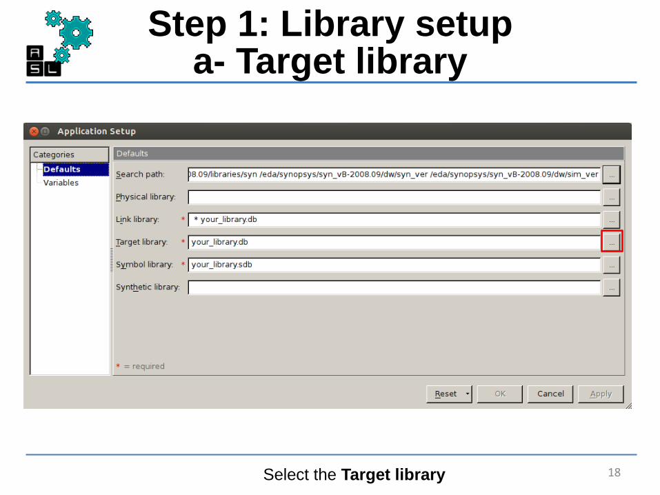
Step 1: Library setupa- Target library
Select the Target library 18

Step 1: Library setupa- Target library
Click on you_library.db to modify the default library 19

Step 1: Library setupa- Target library
Go to ~/lib and select typical.db.
Click Open20

Step 1: Library setupb- Symbol library
Select the Symbol library 21

Step 1: Library setupb- Symbol library
Go to ~/lib and select generic.sdb.
Click Open22

Step 1: Library setupc- Synthetic library
Select the Synthetic library 23

Step 1: Library setupc- Synthetic library
Go to ~/lib and select dw_foundation.sldb.
Click Open24

Step 1: Library setupd- Link library
Finally the Link library, should contain the combined path of:
• Current directory: “*”
• Target library: “home/zxp035/lib/typical.db”
• Synthetic library: “/home/zxp035/lib/dw_foundation.sldb”
Click OK 25

Step 2: Analysisa- File selection
After setting the libraries, we should make the analysis of our circuit
Click on File->Analyze26

Step 2: Analysisa- File selection
1- Change the format to Verilog
2- Click Add
1 2
27

Step 2: Analysisa- File selection
Go to ./verilog_src and select the 11 Verilog files of the router
Click Select28

Step 2: Analysisa- File selection
Click OK 29

Step 2: Analysisb- Analysis report
The analysis report will appear in the console window 30

Step 2: Analysisc- Checkpoint
It is recommended to save your progress after each step
1. Click File-> Save As
2. Go to ./checkpoints
3. In File name, type analysis.ddc
4. Change the Format to DDC (ddc)
5. Click Save
31

Step 3: Elaborationa- Top file selection
After Analysis, we should make the Elaboration of our circuit. Click on File->Elaborate
In Design, select the top module of the router router_LAXYZ (verilog)32

Step 3: Elaborationa- Top file selection
Click OK33
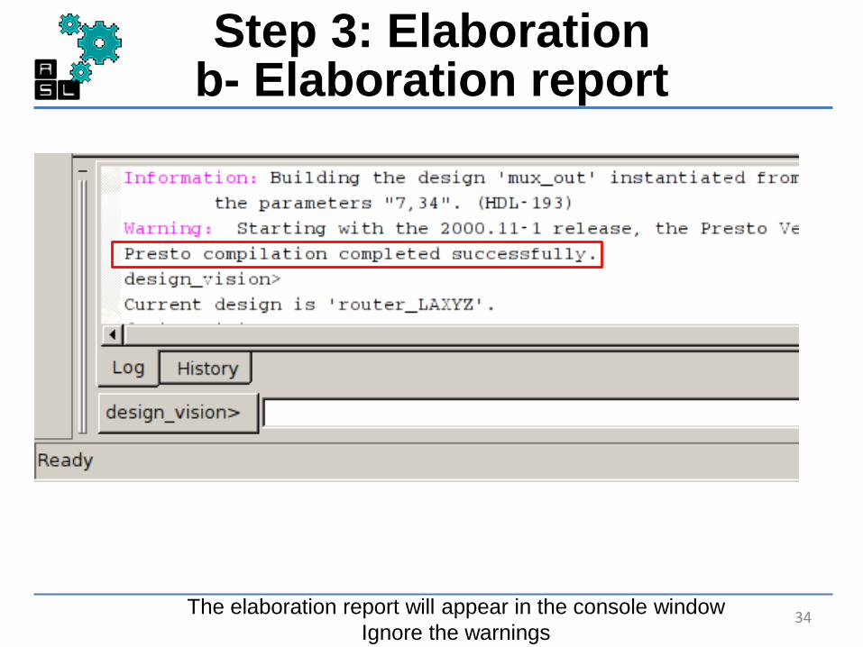
Step 3: Elaborationb- Elaboration report
The elaboration report will appear in the console window
Ignore the warnings34

Step 3: Elaborationc- Hierarchy
The design hierarchy can be seen on the left side of the window 35

Step 3: Elaborationd- Schematic
The design schematic can be seen by clicking on this icon at the top of the window 36

Step 3: Elaboratione- Checkpoint
1. Click File-> Save As
2. Go to ./checkpoints
3. In File name, type elaboration.ddc
4. Make sure the Format is DDC (ddc)
5. Click Save
37
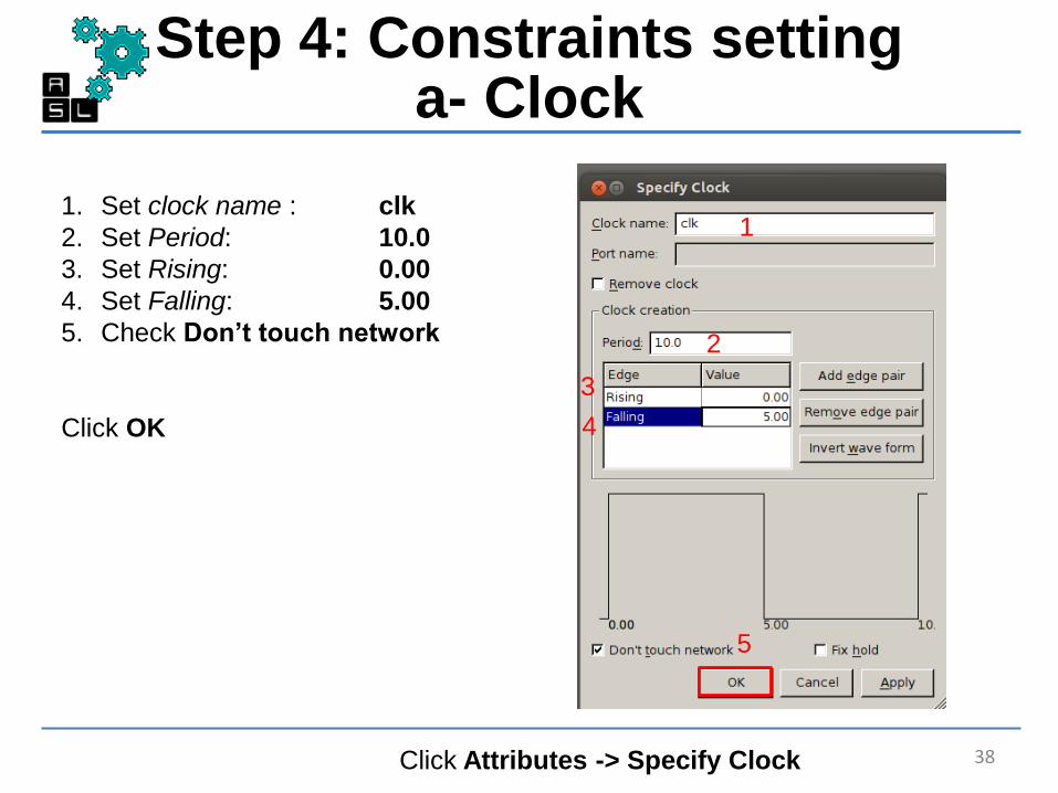
Step 4: Constraints settinga- Clock
Click Attributes -> Specify Clock
1
2
3
4
5
1. Set clock name : clk
2. Set Period: 10.0
3. Set Rising: 0.00
4. Set Falling: 5.00
5. Check Don’t touch network
Click OK
38
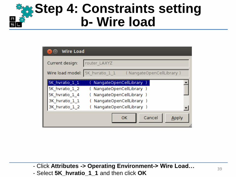
Step 4: Constraints settingb- Wire load
- Click Attributes -> Operating Environment-> Wire Load…
- Select 5K_hvratio_1_1 and then click OK39

Step 5: Compilation
- Click Design-> Compile Design
1. Set Map effort to high
2. Check Incremental mapping
Click OK
40

Step 6: Reporta- Area
Click on Design-> Report Area then OK. 41

Step 6: Reporta- Area
In this library the wire load models do not include area information (Wire load has zero
net area) so the Net Interconnect area (and therefore Total area) is left undefined.
The area is measured in micrometer (um)
42

Step 6: Reportb- Power
Click on Design-> Report Power then OK. 43

Step 6: Reportb- Power
The report shown above should appear giving information about Cell Internal
Power, Net Switching Power, Total Dynamic Power, and the Cell Leakage
Power, in addition to their percentage from the total power consumption.
44

Step 7: Output filesa- Verilog file
After finishing the compilation, we should generate the necessary files for the next
Place&Route step
1. Click File-> Save As
2. Go to ./output_files
3. In File name, type router_LAXYZ.vnet
4. Change the Format to Verilog (V)
5. Click Save
45

Step 7: Output filesb- sdc file
In the dc_shell window type the following command to save the .sdc file
write_sdc ./output_files/router_LAXYZ.sdc
46

Step 7: Output filese- checkpoint
1. Click File-> Save As
2. Go to ./checkpoints
3. In File name, type router_LAXYZ.ddc
4. Make sure the Format is DDC (ddc)
5. Click Save
Final checkpoint save 47

Scripts
• The 7 steps previously presented can be made via commands inserted in the dc_shell.
• The commands required for the synthesis are grouped in a single .tcl file.
• The .tcl file is named “syn_LAXYZ.tcl”
• It is located in:“/home/zxp035/3D_ONoC/Synthesis/script
48

Script
To run the TCL script, click File> Execute script
Go to ./scripts, select syn_LAXYZ.tcl and click Open49

Script: syn_LAFT.tcl (1/3)
#### Define the variable which we will use ####
set base_name "router_LAXYZ"
set clock_name "clk"
set clock_period 10.0
#### Step 1: Set the libraries: ####
set target_library "~/lib/typical.db"
set synthetic_library "~/lib/dw_foundation.sldb“
set link_library [concat "*" $target_library $synthetic_library]
set symbol_library ""~/lib/generic.sdb“
define_design_lib WORK -path ./WORK # redirect the log files to a new folder “WORK”
#### Step 2: Analysis ####
analyze -format verilog {./verilog_src/crossbar.v ./verilog_src/defines.v ./verilog_src/fifo.v./verilog_src/input_port.v ./verilog_src/matrix_arb_formultistage.v ./verilog_src/mux_out.v./verilog_src/request_cntrl.v ./verilog_src/route.v ./verilog_src/router_LAXYZ.v./verilog_src/stop_go.v ./verilog_src/sw_alloc.v}
50

Script: syn_LAFT.tcl (2/3)
# Analysis checkpoint
write_file -format ddc -hierarchy -output ./checkpoints/analysis.ddc
#### Step 3: Elaboration####
elaborate $base_name
# Elaboration checkpoint
write_file -format ddc -hierarchy -output ./checkpoints/elaboration.ddc
#### Step 4: Constraints####
# Clock
create_clock -name $clock_name -period $clock_period [find port $clock_name]
set_clock_uncertainty 0.02 [get_clocks $clock_name]
# Delay
set_input_delay 0.1 -clock clk [remove_from_collection [all_inputs] {clk reset}]
set_output_delay 0.1 -clock clk [all_outputs]
# Wire load
set_wire_load_model -name 5K_hvratio_1_1 -library NangateOpenCellLibrary
51

Script: syn_LAFT.tcl (3/3)
#### Step 5: Compilation####
compile -map_effort high
compile -incremental_mapping -map_effort high
#### Step 6: Report####
# Summary report to be saved under the “reports” folder
report_qor > ./reports/Summary_report_${base_name}.txt
# Hierarchical area report to be saved under the “reports” folder
report_area -hierarchy > ./reports/report_area_${base_name}.txt
#### Step 7: Output files ####
# verilog file
write -format verilog -hierarchy -output ./output_files/${base_name}.vnet
# sdc file
write_sdc ./output_files/${base_name}.sdc
# Final checkpoint
write_file -format ddc -hierarchy -output ./DB/${base_name}.ddc
52

2. Place & Route
53
<== Back to Contents

Requirements
• After we finished the synthesis phase, we proceed to perform the Place and Route of 3D-ONoC router with Cadence SoC Encounter.
• For this phase, we need the .vnet and .sdc files obtained from the synthesise phase and which are located in: ~/3D-ONoC/Synthesis/output_files
• We also need the .lib and .lef library files which are located in: ~/lib
54

Place and Routedirectory structure
Path: ~/3D-NoC
Synthesis
checkpoints
Contains the checkpoints
saved all along P&R tutorial
input_files
Contains the files necessary
files for the Place and
Route phase(.V and .sdc)
script
Contains the par_LAXYZ.tclshell script file
reports
Contains the reports
generated from the post
P&R compilation
P&R Readme.txt
55

Place and Routedirectory structure
You can check the complete Synthesis directory and file structure by typing:
tree Synthesis under the “3D_ONoC” directory 56

Environment
Make sure that you are working under cshr environment. Otherwise type tcsh.
Go to /home/zxp035/3D-ONoC/P&R where the P&R folder is located
57
Environment
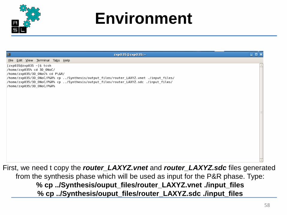
First, we need t copy the router_LAXYZ.vnet and router_LAXYZ.sdc files generated
from the synthesis phase which will be used as input for the P&R phase. Type:
% cp ../Synthesis/ouput_files/router_LAXYZ.vnet ./input_files
% cp ../Synthesis/ouput_files/router_LAXYZ.sdc ./input_files
58

Environment
Type velocity to start SoC Encounter
59
SoC Encounter:P&R steps
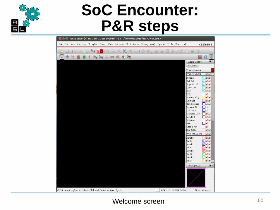
Welcome screen 60

Step 1: Import Design
Click on File->Import Design
Click Files to import the netlist61

Step 1: Import Designa- Netlist (.vnet)
1. Click on >> to expand
2. Go to ./input_files folder
3. Double click on router_LAXYZ.vnet
4. Click Close
2
3
4
1
62

Step 1: Import Designb- Top module
1. In Top Cell: type router_LAXYZ
2. Click on LEF files
2
1
63

Step 1: Import Designc- LEF file
1. Click on >> to expand
2. Go to ~/lib folder
3. Double click on NangateOpenCellLibrary.lef
4. Click Close
2
3
1
4
64

Step 1: Import Designd- Advanced settings
1. Click on Advanced
2. In IPO/CTS type CLKBUF_X1 CLKBUF_X2 CLKBUF_X3
1
2
65

Step 1: Import Designd- Advanced settings
1. In Power type:
a. VDD in Power nets
b. VSS in Ground Nets
2. Click back on Basic
(DO NOT click on OK)
1
2
66

Step 1: Import Designe- Analysis Configuration
Click on Create Analysis Configuration
67

Step 1: Import Designe- Analysis Configuration
1. Double click on Library Sets in the MMMC Browser window
2. On the add Library Set window, type default in Name
3. Click on Add.
4. In the Timing Library Window, go to ~/lib and select typical.lib
5. Click Open (Timing Library Window) and then OK (Library Set Window)
1
2
3
4
5
5
4
68

Step 1: Import Designe- Analysis Configuration
1. Double click on Delay Corners in the MMMC browser window
2. On the Add Delay Corner window, type default in Name
3. Change the Library Set to default.
4. Click OK
12
3
4
69

Step 1: Import Designe- Analysis Configuration
1. Double click on Constraint Modes in the MMMC browser window
2. On the Add Constraint Mode window, type default in Name
3. Click on Add.
4. In the SDC Constraint File window, go to ./input_files and select router_LAXYZ.sdc
5. Click Open (SDC Constraint File window) and then OK (Add Constraint Mode window)
1
2
3
4
5
5
70

Step 1: Import Designe- Analysis Configuration
1. Double click on Analysis Views in the MMMC browser window
2. On the Add Analysis View window, type default in Name
3. Click OK
1
2
3
71

Step 1: Import Designe- Analysis Configuration
1. Double click on Setup Analysis Views in the MMMC browser window
2. In the Add Setup Analysis View window, make sure that Analysis View is set to
default
3. Click OK
1
2
3
72

Step 1: Import Designe- Analysis Configuration
1. Double click on Hold Analysis Views in the MMMC browser window
2. In the Add Hold Analysis View Window, make sure that Analysis View is set to
default
3. Click OK
1
2
3
73

Step 1: Import Designe- Analysis Configuration
1. Click on Save&Close… in the MMMC browser window
2. Go to ./input_files
3. Type Default.view in File name
4. Click Save
1
2
3 4
74

Step 1: Import Designf- Result
In the welcome screen, we can see the modules of 3D-ONoC router before placement:
7 input_ports: (ip[0~6]), Switch_allocator (sw_allc), and Crossbar (cbar)
ip[0] ip[1]
ip[5] ip[6]
ip[2] ip[3] ip[4]
cbarsw_allc
75

Step 1: Import Designg- Checkpoint
We should save the progress at each step.
Click File-> Save Design
1. Click in File name
2. Go to ./checkpoints
3. Type import.enc in File name
4. Click Save
5. Click OK
1
2
3
4
5
76

Step 2: Floorplan
In this step we specify the floorplan
Click Floorplan-> Specify Floorplan
1. Check Die Size by:
2. Enter 300 for both Width and Height
3. Enter 15 for
• Core to Left
• Core to Right
• Core to Top
• Core to Bottom
4. Click OK
1
4
2
3
77

Step 2: Floorplan
1. In the main window, the boundaries of the chip appear.
2. Save your design under floorplan.enc in ./checkpoints directory78

Step 3: Power Ring
Click on Power-> Power Planning->Add Ring …
1. Input VDD VSS in Nets(s):
2. Change the layer to:
• metal 10 V for Top and Bottom
• metal 9 H for Left and Right
3. Change the Width to 4
4. Change the Spacing to 2
5. Check Center in channel
6. Click OK
1
23
4
6
5
79
Step 3: Power Ring
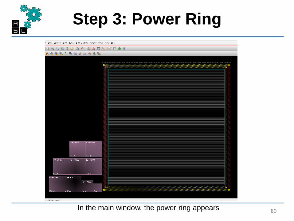
In the main window, the power ring appears 80

Step 4: Power Stripe
Click on Power-> Power Planning->Add Stripe …
1. Input VDD VSS in Nets(s):
2. Change Layer to metal 8
3. Set:
• Width to 4
• Spacing to 2
4. Change Set-to-set- distance to 50
5. Change the Relative from core or
selected area: X from Left to 35
6. Click OK
12
3
4
5
6
81

Step 4: Power Stripe
In the main window, the power stripes appears 82

Step 5: Power Routing
- Click on Route> Special Route
- Input VDD VSS in Nets(s):
- Click OK
83

Step 5: Power Routing
1. In the main window, the power routing appears
2. Save your design under power.enc in ./checkpoints directory84

Step 6: Placement
Now we place the 3D_ONoC modules on the die:
- Click Place-> Place Standard Cell.
- Click OK
85

Step 6: Placement
In the main window, click on to view the placed modules
ip[0]
ip[1]
ip[4]ip[6]
ip[2]
ip[3]
ip[5]
cbar
sw_allc
86

Step 6: Placement
In the main window, click on for the physical view 87

Step 7: Clock Treea- Synthesize
1. Click on Gen Spec
2. Select CLKBUF_X1 CLKBUF_X2 CLKBUF_X3
3. Click OK (Generate clock spec window)
4. Click OK (Synthesize Clock Tree)
1
2
34
Click on Clock-> Synthesize Clock Tree 88

Step 7: Clock Treeb- Display
Click on Clock ->Display -> Display Clock Tree
1. Check Clock Route Only
2. Check Display Clock Tree
3. Click OK
89

Step 7: Clock Tree
1. In the main window, the clock tree appears
2. Save your design under clock_syn.enc in ./checkpoints directory90

Step 8: Nano Routea- Setting
Click on Route-> NanoRoute-> Route
Check Time Driven and then click OK91
Step 8: Nano Routeb- Report
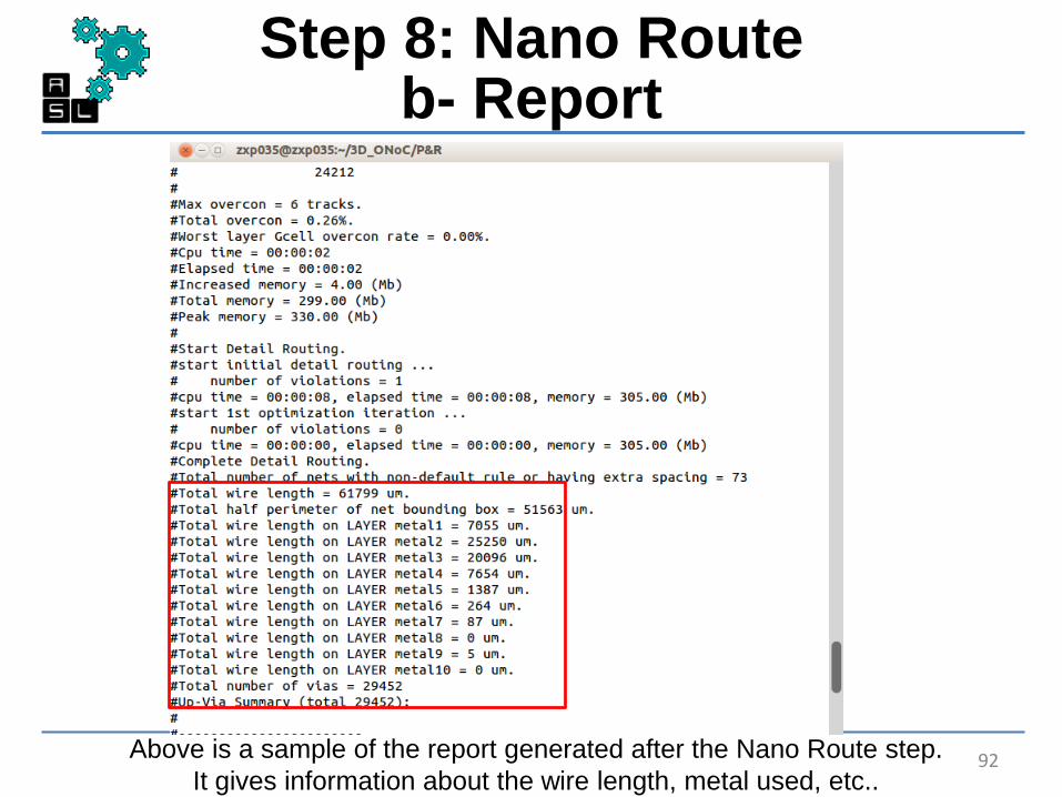
Above is a sample of the report generated after the Nano Route step.
It gives information about the wire length, metal used, etc..92

Step 9: Optimizationa- setting
Click on Optimize-> Optimize Design
1. Check Post-Route
2. Check Hold
3. Click OK
93

Step 9: Optimizationb- report
Above is a sample of the report generated after the Optimization step.
It gives information about the Setup and Hold violations, used metal layers thikness, etc.. 94

Step 10: Adding Fillers
Click on Place -> Physical Cells->Add Filler
1. Check Select
2. Select FILLCELL_X1,2,4,8,16,32
3. Click ADD
4. Click Close
5. Click OK
1
2
3
4
5
95

Step 10: Adding Fillers
1. Save your final design under final.enc in ./checkpoints directory 96

Step 11: Design checkinga- Layout Vs. Schematic (LVS)
Click Verify->Verify Connectivity
Save the Verify Connectivity Report.rpt under ./reports, and then click OK
Report displayed on the terminal
97

Step 11: Design checkingb- Design Rule Check (DRC)
Click Verify->Verify geometry
Under Advanced, save the Verify Geometry Report.rpt under ./reports.
Click OK
Report displayed on the terminal
98

Step 12: Output filesa- SPEF file
We save the output files of the Place&Route phase under ./reports
1. Click on Timing-> Extract RC
2. Check Save SPEF to
3. Click OK
99

Step 12: Output filesb- SDF file
We save the output files of the Place&Route phase under ./reports
1. Click on Timing-> Extract RC
2. Save the SDF Output File in ./reports
3. Click OK
100

Step 12: Output filesc- Netlist file
We save the output files of the Place&Route phase under ./reports
1. Click on File-> Save-> Netlist
2. Save the router_LAXYZ_final.vnet in ./reports
3. Click OK
101

Scripts
• The 12 steps previously presented can be made via commands inserted in the SoC Encounter terminal.
• The commands required for the Place&Route are grouped in a single .tcl file.
• The .tcl file is named “par_LAXYZ.tcl”
• It is located in:“/home/zxp035/3D-ONoC/P&R/script ”
• To run the TCL script type on your terminal:
velocity 1> source /3D-NoC/P&R/script/par_LAXYZ.tcl
102

Script: par_LAFT.tcl (1/8)
################################## Start tutorial #################################
#
# Step 1: Setup (File --> Import Design)
#
setUIVar rda_Input ui_netlist ./input_files/router_LAXYZ.vnet
setUIVar rda_Input ui_timingcon_file ./ input_files/router_LAXYZ.sdc
setUIVar rda_Input ui_topcell router_LAXYZ
setUIVar rda_Input ui_leffile ~/lib/NangateOpenCellLibrary.lef
setUIVar rda_Input ui_timelib ~/lib/typical.lib
setUIVar rda_Input ui_pwrnet VDD
setUIVar rda_Input ui_gndnet VSS
setUIVar rda_Input ui_cts_cell_list {CLKBUF_X1 CLKBUF_X2 CLKBUF_X3}
commitConfig
# Checkpoint
saveDesign import.enc
103
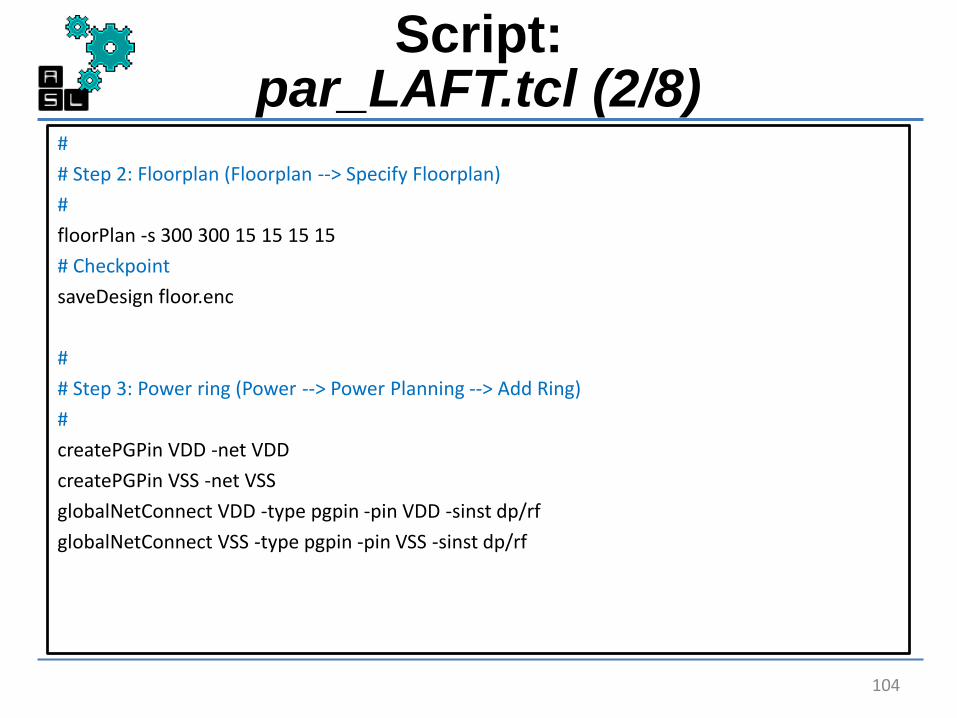
Script: par_LAFT.tcl (2/8)
#
# Step 2: Floorplan (Floorplan --> Specify Floorplan)
#
floorPlan -s 300 300 15 15 15 15
# Checkpoint
saveDesign floor.enc
#
# Step 3: Power ring (Power --> Power Planning --> Add Ring)
#
createPGPin VDD -net VDD
createPGPin VSS -net VSS
globalNetConnect VDD -type pgpin -pin VDD -sinst dp/rf
globalNetConnect VSS -type pgpin -pin VSS -sinst dp/rf
104

Script: par_LAFT.tcl (3/8)
addRing -nets {VSS VDD} -type core_rings \
-spacing_top 2 -spacing_bottom 2 -spacing_right 2 -spacing_left 2 \
-width_top 4 -width_bottom 4 -width_right 4 -width_left 4 \
-around core -jog_distance 0.095 -threshold 0.095 \
-layer_top metal10 -layer_bottom metal10 -layer_right metal9 \
-layer_left metal9 \
-stacked_via_top_layer metal10 -stacked_via_bottom_layer metal1
#
# Step 4: Power stripe (Power --> Power Planning --> Add Stripe)
#
addStripe -nets {VSS VDD} -layer metal8 -width 2 -spacing 1.5 \
-block_ring_top_layer_limit metal9 -block_ring_bottom_layer_limit metal7 \
-padcore_ring_top_layer_limit metal9 -padcore_ring_bottom_layer_limit metal7 \
-stacked_via_top_layer metal10 -stacked_via_bottom_layer metal1 \
-set_to_set_distance 50 -xleft_offset 50 -merge_stripes_value 0.095 \
-max_same_layer_jog_length 1.6
105

Script: par_LAFT.tcl (4/8)
#
# Step 5: Power route (Route --> Special Router)
#
sroute -nets {VSS VDD} -layerChangeRange {1 10} \
-connect { blockPin padPin padRing corePin floatingStripe } \
-blockPinTarget { nearestRingStripe nearestTarget } \
-padPinPortConnect { allPort oneGeom } \
-checkAlignedSecondaryPin 1 -blockPin useLef -allowJogging 1 \
-crossoverViaBottomLayer 1 -allowLayerChange 1 -targetViaTopLayer 10 \
-crossoverViaTopLayer 10 -targetViaBottomLayer 1
# Checkpoint
saveDesign power.enc
#
# Step 6: Placement (Place --> Standard Cell)
#
placeDesign -prePlaceOpt
106

Script: par_LAFT.tcl (5/8)
#
# Step 7: Clock tree synthesis (CTS)
#a- Synthesis: (Clock --> Synthesize Clock Tree)
addCTSCellList {CLKBUF_X1 CLKBUF_X2 CLKBUF_X3}
clockDesign -genSpecOnly Clock.ctstch
clockDesign -specFile Clock.ctstch -outDir clock_report -fixedInstBeforeCTS
# Checkpoint
saveDesign clock_syn.enc
#
# b- Display: (Clock --> Display --> Display Clock Tree)
This step should be done manually
#
107

Script: par_LAFT.tcl (6/8)
#
# Step 8: Detailed route (Route --> Nano Route --> Route)
#
setNanoRouteMode -quiet -routeWithTimingDriven true
setNanoRouteMode -quiet -routeTopRoutingLayer default
setNanoRouteMode -quiet -routeBottomRoutingLayer default
setNanoRouteMode -quiet -drouteEndIteration default
setNanoRouteMode -quiet -routeWithTimingDriven true
routeDesign -globalDetail
#
# Step 9: Optimization (postRoute) (Optimize --> Optimize Design)
#
optDesign -postRoute
optDesign -postRoute -hold
# Checkpoint
saveDesign route.enc
108

Script: par_LAFT.tcl (7/8)
#
# Step 10: Add fillers (Place --> Physical Cells --> Add Filler)
#
addFiller -prefix FILLER -cell FILLCELL_X1 FILLCELL_X2 FILLCELL_X4 \
FILLCELL_X8 FILLCELL_X16 FILLCELL_X32
#
# Step 11: Verification (LVS) (Verify --> Verify Connectivity)
#
verifyConnectivity -type all -error 1000 -warning 50 # LVS check
verifyGeometry # DRC
#
# Step 12: Data out (Timing --> Extract RC, Timing --> Write SDF, File --> Save --> Netlist)
#
saveNetlist router_LAXYZ_final.vnet # Netlist
109

Script: par_LAFT.tcl (8/8)
isExtractRCModeSignoff
rcOut -spef router_LAXYZ.spef # SPEF file
delayCal -sdf router_LAXYZ.sdf –idealclock # SDF file
# Final checkpoint
save Design final.enc
###############################################################################
################################### End tutorial #################################
###############################################################################
110

3. Design checking LVS (Layout-Versus-
Schematic) & Design Rule Check (DRC)
111
<== Back to Contents

Objectives
• In this tutorial, we check the correctness of the designed 3D-ONoC router. Two main checking process are performed in this tutorial:
– Layout Versus Schematic (LVS)
Checks whether the integrated circuit layout in the Place & Route phase (Phase 2) corresponds to the original schematic or circuit diagram of the design obtained in the Design Synthesis phase (Phase 1).
– Design Rule Check (DRC)
• Ensures that the layout conforms to the rules designed/required for faultless fabrication.
112

Requirements
• Before starting the design check, you should have already finished the two previous steps:
– Design synthesis (DS)
– Place & Route (P&R)
• If you are not continuing the previous two steps, you need the final.enc file and file.enc.datfolder to be copied first to the ./checkpoints directory to restore the final post P&R design
113

Design Checkdirectory structure
Path: ~/3D-NoC
Synthesis P&R Readme.txtDesign_check
checkpoint
Contains the last checkpointsaved from P&R tutorial.It will be used to restore thedesign and perform thechecking
114

Contents
• Environment
• Restore design
• Layout Vs. Schematic (LVS)
• Design Rule Check (DRC)
• Commands
115

Environment
- Make sure that you are working under cshr environment. Otherwise type tcsh.
- Go to /home/zxp035/3D-ONoC/ and make Design_check
- In the new Design_check directory, make a new directory checkpoint116

Environment
In the new checkpoint directory, we will copy the last checkpoint performed
in P&R phase. We need to copy final.enc file and final.enc.dat folder117

Environment
Use cp command to copy final.enc file from ../PandR/checkpoints into ./checkpoint
Use cp – r command to copy also final.enc.dat folder118

Environment
Start SoC Encounter 119

Restore design
First, we should restore the final design of the P&R phase
Click File>Restore design
1
2
3
4
5
1. Click on the folder
2. Go to ./checkpoint
3. Select final.enc file
4. Click Open
5. Click OK
120

Restore design
The final layout of the P&R phase should appear 121

Layout Vs. Schematic (LVS)
Click Verify->Verify Connectivity
Save the Verify Connectivity Report.rpt under ./reports, and then click OK
Report displayed on the terminal
122

Design Rule Check (DRC)
Click Verify->Verify geometry
Under Advanced, save the Verify Geometry Report.rpt under ./reports.
Click OK
Report displayed on the terminal
123

Commands
• To perform the Layout Vs. Schematic (LVS) type the following command on your terminal:
• To perform the Design Rule Check (DRC) type the following command on your terminal:
velocity 1> verifyConnectivity -type all -error 1000 -warning 50
velocity 2> verifyGeometry
124

4. Post-Layout simulation
125
<== Back to Contents

Objectives
• After completing this tutorial you will be able to:
– Check if the post-layout design is free from any timing violations
– Report timing and area
– Evaluate the power consumption (dynamic and static)
– Learn how to make the post-layout simulation via:
• The CAD Graphic User Interface
• Tcl script
126

Contents
• Requirements
• Post-layout simulation directory structure
• Setup
• Post layout synthesis (Step 1~3)
• Script
127

Requirements
• Before starting the post-layout, you should have already finished the three previous phases:
– Design Synthesis (DS)
– Place & Route (P&R)
– Design Check (LVS and DCR)
• We should create a new directory:~/3D-ONoC/Post
where the post-layout simulation is performed.
128

Post-layoutdirectory structure
Path: ~/3D-NoC
Synthesis P&R Readme.txtDesign_check
129
input_files
Contains the files necessary
files for the Post-layout
phase(.Vnet, .sdc,
.spef, .sdf, and .sdc)
scripts
Contains the sta_LAXYZ.tcl
and power_LAXYZ.tcl shell script
files
reports
Contains the reports
generated from the post-
layout synthesis
compilation
Post
verilog_src
Contains the Verilog-HDL
source files for the 3D-OASIS-
NOC

Setup
• Before we start, we should copy some output files that we will use for this phase.
– router_LAXYZ_final.vnet (From P&R phase)
– router_LAXYZ_final.spef (From P&R phase)
– router_LAXYZ_final.sdf (From P&R phase)
– router_LAXYZ_final.sdc (From Synthesis phase)
• These files should be copied to ~/3D-ONoC/Post/input
130

Setup
131
Type tcsh and go to ~3D-ONoC/Post
Using the “cp” command, copy the necessary four files to ./input
Start Design Compiler by typing design_vision

Step 1: Timing analysis
132
• For this step, we execute a script that contains the necessary operations for time analysis.
• The operations are almost the same as the ones performed in Phase 2 (Design Synthesis) of this tutorial.
• The sta_LAXYZ.tcl script file needed for this step is located in ./scripts
• Next slides depicts sta_LAXYZ.tcl

Step 1: Timing analysis: sta_LAXYZ.tcl (1/3)
#### Define the variable which we will use ####
set base_name "router_LAXYZ"
set vnet_file "router_LAXYZ_final.vnet"
set spef_file "router_LAXYZ.spef"
set sdf_file "router_LAXYZ.sdf"
set sdc_file "router_LAXYZ.sdc“
#### Step 1: Set the libraries: ####
set target_library "~/lib/typical.db"
set synthetic_library "~/lib/dw_foundation.sldb“
set link_library [concat "*" $target_library $synthetic_library]
set symbol_library ""~/lib/generic.sdb“
define_design_lib WORK -path ./WORK # redirect the log files to a new folder “WORK”
133

Script: sta_LAXYZ.tcl (1/2)
#### Step 2: Read post_layout netlist####
read_file -format verilog ./input/$vnet_file
current_design $base_name
link
#### Delay and RC information####
read_sdc ./input/$sdc_file
read_sdf ./input/$sdf_file
read_parasitics ./input/$spef_file
#### Generate reports####
report_timing > ./reports/timing_report_${base_name}.txt
report_reference -hier > ./reports/reference_report_${base_name}.txt
134

Step 1: Timing analysisExecute the script
135To run the TCL script, click File> Execute script
Go to ./scripts, select sta_LAXYZ.tcl and click Open

Step 1: Timing analysisReports
136Analysis reports for timing and area will be saved in ./reports
The reports contain detailed evaluation of reference (area) and timing delay by module
Timing report Reference report

Step 2: Timing simulation
137
• In this second step, we will check whether our design is free from any delay violation.
• We will use ncverilog and simvision.
• We created a test bench file, named Test.v, in order to evaluate 3D-ONoC router.
• In this test bench, random flits are generated, injected from the 7 input-ports of the router and ejected from the 7 output ports.
• Finally, the correctness of the ejected flits is checked.

Step 2: Timing simulation: a- Hierarchy
router_LAXYZ.v input_port.v
sw_alloc.v
crossbar.v
fifo.v
input_port.v
matrix_arb_formultistage.v
stop_go.v
mux.v
Top level module
138
Test.v
Test bench
Test.v is located in ./verilog_src along with the remaining
Verilog source files
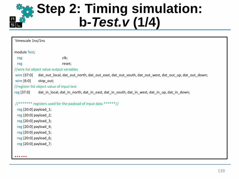
Step 2: Timing simulation: b-Test.v (1/4)
`timescale 1ns/1ns
module Test;
reg clk;
reg reset;
//wire list object value output variables
wire [37:0] dat_out_local, dat_out_north, dat_out_east, dat_out_south, dat_out_west, dat_out_up, dat_out_down;
wire [6:0] stop_out;
//register list object value of input test
reg [37:0] dat_in_local, dat_in_north, dat_in_east, dat_in_south, dat_in_west, dat_in_up, dat_in_down;
//******* registers used for the payload of input data ******//
reg [20:0] payload_1;
reg [20:0] payload_2;
reg [20:0] payload_3;
reg [20:0] payload_4;
reg [20:0] payload_5;
reg [20:0] payload_6;
reg [20:0] payload_7;
……
139

Step 2: Timing simulation: b-Test.v (2/4)
//Top module definition
router_LAXYZ router (.clk(clk),.reset(reset),
.data_in({dat_in_down, dat_in_up, dat_in_west, dat_in_south, dat_in_east, dat_in_north, dat_in_local}),
.data_out({dat_out_down, dat_out_up, dat_out_west, dat_out_south, dat_out_east, dat_out_north, dat_out_local}),
.stop_in({stp_in_local, stp_in_norh, stp_in_east, stp_in_south, stp_in_west, stp_in_up, stp_in_down}),
.stop_in(7'b0000000),
.stop_out(stop_out),
.xaddr(3'b010),.yaddr(3'b010),.zaddr(3'b010)); // We assume that the router has 222 adress
//clock generation (100 Mhz frequency )
always #5000 clk = ~clk;
//Annotation file initialization
initial begin
`ifdef __POST_PR__
$sdf_annotate("input/router_LAXYZ.sdf", Test.router, , "sdf.log", "MAXIMUM");
`endif
#0
clk = 1;
reset = 1'b1;……
140

Step 2: Timing simulation: b-Test.v (3/4)
……#100000
//Initialization of the vcd file that collects simulation information
$dumpfile("dump.vcd");
$dumpvars(0, Test);
//Start sending flits
for(i=0;i<100;i=i+1)begin //We assume the number of sent flit is 100 for simplicity
#10000
//*** local port sending
if(stop_out[0] == 1)
dat_in_local = 0;
else begin
dat_in_local = {payload_1,9'b010011010,7'b0000010,1'b1};//(0,1)
payload_1 = payload_1 + 1;
sent1 = sent1 + 1;
end
…… //*** We perform the same operations for the remaining input-ports
141

Step 2: Timing simulation: b-Test.v (4/4)
end//for loop end
#100000
$finish;
end // initial begin
always @(dat_out_local) begin // Count the flit received at the local out-port
rec1= rec1+1;
end
rec5+1;
end
always @(dat_out_north) begin// Count the flit received at the north out-port
rec2= rec2+1;
end
……// Count the flit received at the remaining out-ports
always @(dat_out_down) begin
rec7= rec7+1;
end
endmodule // The end of Test.v
142
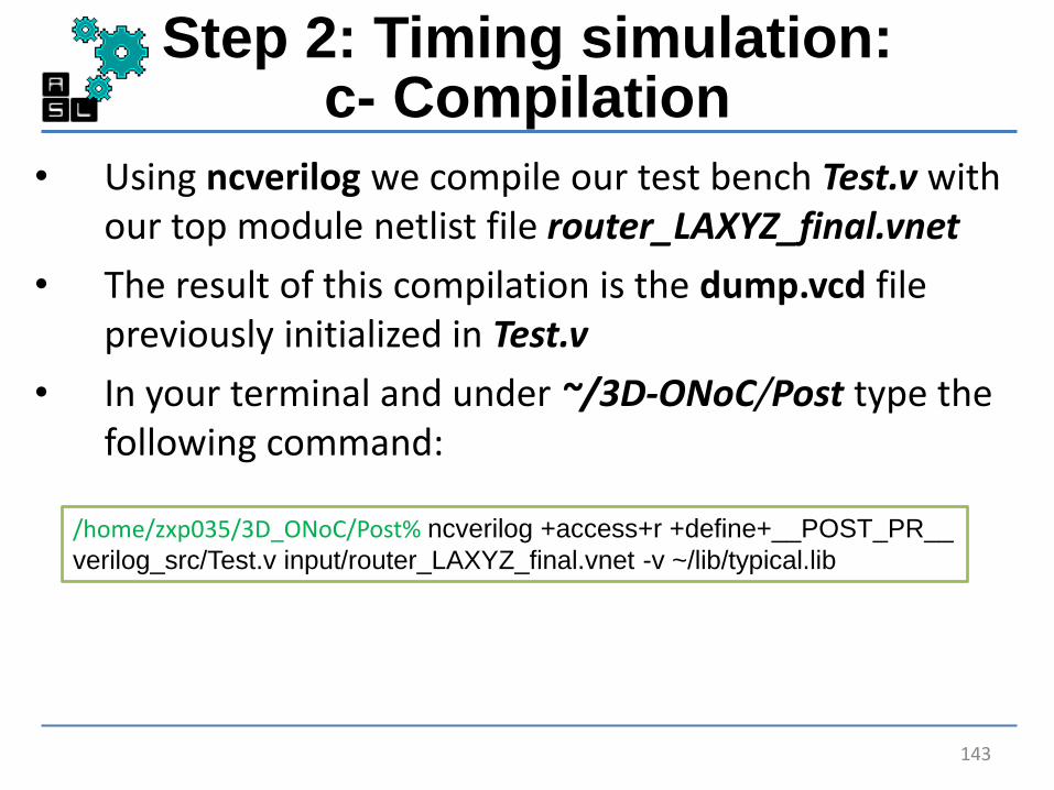
Step 2: Timing simulation: c- Compilation
143
• Using ncverilog we compile our test bench Test.v with our top module netlist file router_LAXYZ_final.vnet
• The result of this compilation is the dump.vcd file previously initialized in Test.v
• In your terminal and under ~/3D-ONoC/Post type the following command:
/home/zxp035/3D_ONoC/Post% ncverilog +access+r +define+__POST_PR__
verilog_src/Test.v input/router_LAXYZ_final.vnet -v ~/lib/typical.lib

Step 2: Timing simulation: d- Simulation
144
• Now, we launch simvision to see the result of the simulation
• In your terminal and under ~/3D-ONoC/Post type the following command:
/home/zxp035/3D_ONoC/Post% simvison &

Step 2: Timing simulation: d- Simulation
145Simvision welcome screen
Click on File> Open Database …

Step 2: Timing simulation: d- Simulation
146
Change Files of type to VCD files (*.vcd)
Select dump.vcd
Click Open

Step 2: Timing simulation: d- Simulation
147
File Translation window will appear
Click on OK to translate dump.vcd into dump.trn
dump.trn file will be used to visualize the test bench signals

Step 2: Timing simulation: d- Simulation
148
Click on Test to see the different variables used in the simulation
Click on to visualize the signals

Step 2: Timing simulation: d- Simulation
149The waveform window appears
Click on to fit the window with your signals

Step 2: Timing simulation: d- Simulation
150
From the waveform we can see that:
- The 100 flits that we sent arrived to their destinations
- No time violations are found, otherwise the signals will be red instead of green

Step 3: Power evaluation
151
• After we made sure that there are no time violations in our design, we proceed to evaluate the power consumption.
• The dump.vcd file contains the switching activities information of the test bench. We need to convert the .vcd file into .saif file.
• The .saif file will be used by Design Compiler Power Anlyzer to evaluate the power
• In your terminal and under ~/3D-ONoC/Post type the following command:
/home/zxp035/3D_ONoC/Post% vcd2saif -input dump.vcd -output router_LAXYZ.saif

Step 3: Power evaluation
152
• For the evaluation, we execute a script that contains the necessary operations for power evaluation.
• The operations are almost the same as in the ones performed in Timing analysis (Step 1) of this post_layout simulation phase.
• The power_LAXYZ.tcl script file needed for this step is located in ./scripts
• Next slides present power_LAXYZ.tcl file

Step 3: Power evaluationpower_LAXYZ.tcl (1/2)
#### Define the variable which we will use ####
set base_name "router_LAXYZ"
set vnet_file "router_LAXYZ_final.vnet"
set spef_file "router_LAXYZ.spef"
set sdf_file "router_LAXYZ.sdf"
set sdc_file "router_LAXYZ.sdc“
set saif_file "router_LAXYZ.saif“
#### Step 1: Set the libraries: ####
set target_library "~/lib/typical.db"
set synthetic_library "~/lib/dw_foundation.sldb“
set link_library [concat "*" $target_library $synthetic_library]
set symbol_library ""~/lib/generic.sdb“
define_design_lib WORK -path ./WORK # redirect the log files to a new folder “WORK”
153

Step 3: Power evaluationpower_LAXYZ.tcl (1/2)
#### Step 2: Read post_layout netlist####
read_file -format verilog ./input/$vnet_file
current_design $base_name
link
#### Delay and RC information####
read_sdc ./input/$sdc_file
read_sdf ./input/$sdf_file
read_parasitics ./input/$spef_file
#### Read switching activities information####
reset_switching_activity
read_saif -input $saif_file -instance top/dut -unit ns -scale 1
#### Generate reports####
report_timing > ./reports/timing_report_${base_name}.txt
report_reference -hier > ./reports/reference_report_${base_name}.txt
report_power -hier > ./reports/power_report_${base_name}.txt
154

Step 3: Power evaluation Execute the script
155To run the TCL script, click File> Execute script in Design Compiler
Go to ./scripts, select power_LAXYZ.tcl and click Open
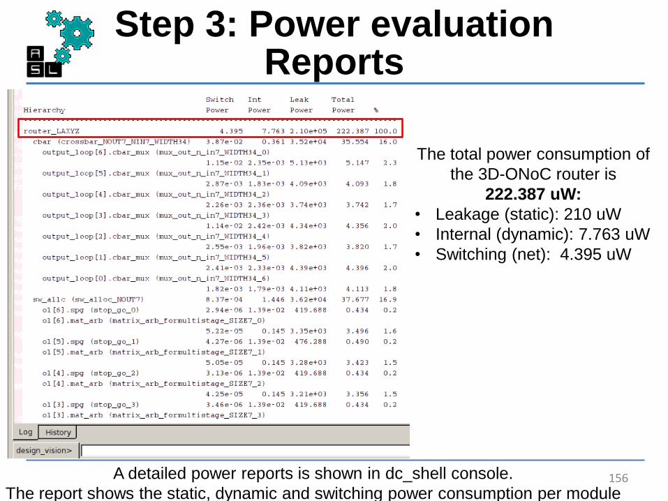
Step 3: Power evaluationReports
156A detailed power reports is shown in dc_shell console.
The report shows the static, dynamic and switching power consumption per module
The total power consumption of
the 3D-ONoC router is
222.387 uW:
• Leakage (static): 210 uW
• Internal (dynamic): 7.763 uW
• Switching (net): 4.395 uW

5. Pad Insertion
<== Back to Contents

Objectives
• After completing this tutorial you will be able to:
– Reperform the Place and Route phase while inserting the Input/Output (IO) pads
– Establish the connection between the IO pins/ IO pads, and the input signals of 3D-ONoC router
– Generate the final netlist and other output files
• This tutorial is performed is based on modifying input-files and creating a TCL script
158

Contents
• Requirements
• Pad Insertion directory structure
• Environment
• Step 1: Modify router_LAXYZ.vnet
• Step 2: Make router_LAXYZ.io
• Step 3: Make Iopad_LAXYZ.tcl script
• Step 4: Script execution
• Final layout

Requirements
• Before starting the post-layout, you should have already finished the four previous phases:
– Design Synthesis (DS)
– Place & Route (P&R)
– Design Check (LVS and DCR)
– Post-layout simulations
• We should create a new directory:~/3D-ONoC/Iopad
where the IO pad insertion is performed.
160

Post-layoutdirectory structure
Path: ~/3D-NoC
Synthesis P&R Readme.txtDesign_check
161
script
Contains the ioapad.tcl shell
script
checkpoints
Contains the checkpoints
saved all along P&R tutorial
output
Contains the final output-
files generated from the IO
pad insertion
Post
input_files
Contains the files necessary
files for the pad-insertion phase (.vnet, .sdc, and ,io)
Iopad

Environment
Make sure that you are working under cshr environment. Otherwise type tcsh.
Go to /home/zxp035/3D-ONoC/Iopad where the Pad folder is located
$ tcsh/home/zxp035/3D-ONoC% cd Iopad//home/zxp035/3D-ONoC/Pad%

Environment
First, we need t copy the router_LAXYZ.vnet and router_LAXYZ.sdc files generated
from the synthesis phase which will be used as input for the Pad insertion phase. Type:
% cp ../Synthesis/ouput_files/router_LAXYZ.vnet ./input
% cp ../Synthesis/ouput_files/router_LAXYZ.sdc ./input
% cp ../Synthesis/output_files/router_LAXYZ.vnet ./input% cp ../Synthesis/output_files/router_LAXYZ.sdc ./input

Step 1:Modify router_LAXYZ.vnet (1/6)
module router_LAXYZ ( clk_pad, reset_pad, data_in_pad, data_out_pad, stop_in_pad, stop_out_pad, xaddr_pad,
yaddr_pad, zaddr_pad );
input [265:0] data_in_pad;
output [265:0] data_out_pad;
input [6:0] stop_in_pad;
output [6:0] stop_out_pad;
input [2:0] xaddr_pad;
input [2:0] yaddr_pad;
input [2:0] zaddr_pad;
input clk_pad, reset_pad;
wire [265:0] data_in;
wire [265:0] data_out;
wire [6:0] stop_in;
wire [6:0] stop_out;
wire [2:0] xaddr;
wire [2:0] yaddr;
wire [2:0] zaddr;

wire clk, reset;
wire n1, n2, n3, n4, n5, n6, n7;
wire [265:0] cbar_data_in;
wire [6:0] sw_req;
wire [48:0] port_req;
wire [6:0] sw_grant;
wire [6:0] data_sent;
wire [48:0] sw_cntrl;
CORNER_PAD corner_0_inst ();
IN_PAD data_in_0_inst ( .PAD(data_in_pad[0]), .O(data_in[0]) );
IN_PAD data_in_1_inst ( .PAD(data_in_pad[1]), .O(data_in[1]) );
// ...
// Repeat
// ...
IN_PAD data_in_137_inst ( .PAD(data_in_pad[137]), .O(data_in[137]) );
IN_PAD data_in_138_inst ( .PAD(data_in_pad[138]), .O(data_in[138]) );
VDD_PAD vdd_0_inst ();
VSS_PAD vss_0_inst ();
Step 1:Modify router_LAXYZ.vnet (2/6)

CORNER_PAD corner_1_inst ();
IN_PAD data_in_139_inst ( .PAD(data_in_pad[139]), .O(data_in[139]) );
IN_PAD data_in_140_inst ( .PAD(data_in_pad[140]), .O(data_in[140]) );
IN_PAD data_in_141_inst ( .PAD(data_in_pad[141]), .O(data_in[141]) );
// ...
// Repeat
// ...
IN_PAD data_in_264_inst ( .PAD(data_in_pad[264]), .O(data_in[264]) );
IN_PAD data_in_265_inst ( .PAD(data_in_pad[265]), .O(data_in[265]) );
OUT_PAD data_out_0_inst ( .PAD(data_out_pad[0]), .I(data_out[0]) );
OUT_PAD data_out_1_inst ( .PAD(data_out_pad[1]), .I(data_out[1]) );
OUT_PAD data_out_2_inst ( .PAD(data_out_pad[2]), .I(data_out[2]) );
OUT_PAD data_out_3_inst ( .PAD(data_out_pad[3]), .I(data_out[3]) );
OUT_PAD data_out_4_inst ( .PAD(data_out_pad[4]), .I(data_out[4]) );
OUT_PAD data_out_5_inst ( .PAD(data_out_pad[5]), .I(data_out[5]) );
OUT_PAD data_out_6_inst ( .PAD(data_out_pad[6]), .I(data_out[6]) );
OUT_PAD data_out_7_inst ( .PAD(data_out_pad[7]), .I(data_out[7]) );
OUT_PAD data_out_8_inst ( .PAD(data_out_pad[8]), .I(data_out[8]) );
OUT_PAD data_out_9_inst ( .PAD(data_out_pad[9]), .I(data_out[9]) );
OUT_PAD data_out_10_inst ( .PAD(data_out_pad[10]), .I(data_out[10]) );
OUT_PAD data_out_11_inst ( .PAD(data_out_pad[11]), .I(data_out[11]) );
Step 1:Modify router_LAXYZ.vnet (3/6)

VDD_PAD vdd_1_inst ();
VSS_PAD vss_1_inst ();
CORNER_PAD corner_2_inst ();
OUT_PAD data_out_12_inst ( .PAD(data_out_pad[12]), .I(data_out[12]) );
OUT_PAD data_out_13_inst ( .PAD(data_out_pad[13]), .I(data_out[13]) );
OUT_PAD data_out_14_inst ( .PAD(data_out_pad[14]), .I(data_out[14]) );
// ...
// Repeat
// ...
OUT_PAD data_out_146_inst ( .PAD(data_out_pad[146]), .I(data_out[146]) );
OUT_PAD data_out_147_inst ( .PAD(data_out_pad[147]), .I(data_out[147]) );
OUT_PAD data_out_148_inst ( .PAD(data_out_pad[148]), .I(data_out[148]) );
OUT_PAD data_out_149_inst ( .PAD(data_out_pad[149]), .I(data_out[149]) );
OUT_PAD data_out_150_inst ( .PAD(data_out_pad[150]), .I(data_out[150]) );
VDD_PAD vdd_2_inst ();
VSS_PAD vss_2_inst ();
Step 1:Modify router_LAXYZ.vnet (4/6)

OUT_PAD data_out_264_inst ( .PAD(data_out_pad[264]), .I(data_out[264]) );
OUT_PAD data_out_265_inst ( .PAD(data_out_pad[265]), .I(data_out[265]) );
IN_PAD stop_in_0_inst ( .PAD(stop_in_pad[0]), .O(stop_in[0]) );
IN_PAD stop_in_1_inst ( .PAD(stop_in_pad[1]), .O(stop_in[1]) );
IN_PAD stop_in_2_inst ( .PAD(stop_in_pad[2]), .O(stop_in[2]) );
IN_PAD stop_in_3_inst ( .PAD(stop_in_pad[3]), .O(stop_in[3]) );
IN_PAD stop_in_4_inst ( .PAD(stop_in_pad[4]), .O(stop_in[4]) );
IN_PAD stop_in_5_inst ( .PAD(stop_in_pad[5]), .O(stop_in[5]) );
IN_PAD stop_in_6_inst ( .PAD(stop_in_pad[6]), .O(stop_in[6]) );
OUT_PAD stop_out_0_inst ( .PAD(stop_out_pad[0]), .I(stop_out[0]) );
OUT_PAD stop_out_1_inst ( .PAD(stop_out_pad[1]), .I(stop_out[1]) );
OUT_PAD stop_out_2_inst ( .PAD(stop_out_pad[2]), .I(stop_out[2]) );
OUT_PAD stop_out_3_inst ( .PAD(stop_out_pad[3]), .I(stop_out[3]) );
OUT_PAD stop_out_4_inst ( .PAD(stop_out_pad[4]), .I(stop_out[4]) );
OUT_PAD stop_out_5_inst ( .PAD(stop_out_pad[5]), .I(stop_out[5]) );
OUT_PAD stop_out_6_inst ( .PAD(stop_out_pad[6]), .I(stop_out[6]) );
Step 1:Modify router_LAXYZ.vnet (5/6)

IN_PAD xaddr_0_inst ( .PAD(xaddr_pad[0]), .O(xaddr[0]) );
IN_PAD xaddr_1_inst ( .PAD(xaddr_pad[1]), .O(xaddr[1]) );
IN_PAD xaddr_2_inst ( .PAD(xaddr_pad[2]), .O(xaddr[2]) );
IN_PAD yaddr_0_inst ( .PAD(yaddr_pad[0]), .O(yaddr[0]) );
IN_PAD yaddr_1_inst ( .PAD(yaddr_pad[1]), .O(yaddr[1]) );
IN_PAD yaddr_2_inst ( .PAD(yaddr_pad[2]), .O(yaddr[2]) );
IN_PAD zaddr_0_inst ( .PAD(zaddr_pad[0]), .O(zaddr[0]) );
IN_PAD zaddr_1_inst ( .PAD(zaddr_pad[1]), .O(zaddr[1]) );
IN_PAD zaddr_2_inst ( .PAD(zaddr_pad[2]), .O(zaddr[2]) );
IN_PAD clk_inst ( .PAD(clk_pad), .O(clk ) );
IN_PAD reset_inst ( .PAD(reset_pad), .O(reset) );
VDD_PAD vdd_3_inst ();
VSS_PAD vss_3_inst ();
OR4_X1 U15 ( .A1(data_out[155]), .A2(data_out[154]), .A3(data_out[153]),
.A4(n3), .ZN(data_sent[4]) );
OR4_X1 U16 ( .A1(data_out[157]), .A2(data_out[156]), .A3(data_out[159]),
.A4(data_out[158]), .ZN(n3) );
// …
Step 1:Modify router_LAXYZ.vnet (6/6)

Step 2:Make router_LAXYZ.io(1/5)
(globals
version = 3
io_order = default
)
(iopad
(topleft
(inst name="corner_0_inst")
)
(top
(inst name="data_in_0_inst")
(inst name="data_in_1_inst")
//… repeat …
(inst name="data_in_137_inst")
(inst name="data_in_138_inst")
(inst name="vdd_0_inst")
(inst name="vss_0_inst")
)
(topright
(inst name="corner_1_inst")
)

Step 2: Make router_LAXYZ.io(2/5)
(right
(inst name="data_in_139_inst")
(inst name="data_in_140_inst“)
// … repeat …
(inst name="data_in_264_inst")
(inst name="data_in_265_inst")
(inst name="data_out_0_inst")
(inst name="data_out_1_inst")
(inst name="data_out_2_inst")
(inst name="data_out_3_inst")
(inst name="data_out_4_inst")
(inst name="data_out_5_inst")
(inst name="data_out_6_inst")
(inst name="data_out_7_inst")
(inst name="data_out_8_inst")
(inst name="data_out_9_inst")
(inst name="data_out_10_inst")
(inst name="data_out_11_inst")
(inst name="vdd_1_inst")
(inst name="vss_1_inst")
)

Step 2: Make router_LAXYZ.io(3/5)
(bottomright
(inst name="corner_2_inst")
)
(bottom
(inst name="data_out_12_inst")
(inst name="data_out_13_inst")
// … repeat …
(inst name="data_out_149_inst")
(inst name="data_out_150_inst")
(inst name="vdd_2_inst")
(inst name="vss_2_inst")
)
(bottomleft
(inst name="corner_3_inst")
)
(left
(inst name="data_out_151_inst")
(inst name="data_out_152_inst")
// … repeat …
(inst name="data_out_264_inst")
(inst name="data_out_265_inst")

Step 2: Make router_LAXYZ.io(4/5)
(inst name="stop_in_0_inst")
(inst name="stop_in_1_inst")
(inst name="stop_in_2_inst")
(inst name="stop_in_3_inst")
(inst name="stop_in_4_inst")
(inst name="stop_in_5_inst")
(inst name="stop_in_6_inst")
(inst name="stop_out_0_inst")
(inst name="stop_out_1_inst")
(inst name="stop_out_2_inst")
(inst name="stop_out_3_inst")
(inst name="stop_out_4_inst")
(inst name="stop_out_5_inst")
(inst name="stop_out_6_inst")
(inst name="xaddr_0_inst")
(inst name="xaddr_1_inst")
(inst name="xaddr_2_inst")

Step 2: Make router_LAXYZ.io(5/5)
(inst name="yaddr_0_inst")
(inst name="yaddr_1_inst")
(inst name="yaddr_2_inst")
(inst name="zaddr_0_inst")
(inst name="zaddr_1_inst")
(inst name="zaddr_2_inst")
(inst name="clk_inst")
(inst name="reset_inst")
(inst name="vdd_3_inst")
(inst name="vss_3_inst")
)
)

Step 3: Make iopad_LAXYZ.tcl (1/9)
#
# Step 1: Setup (File --> Import Design)
#
setUIVar rda_Input ui_netlist ./input_files/router_LAXYZ.vnet
setUIVar rda_Input ui_timingcon_file ./input_files/router_LAXYZ.sdc
setUIVar rda_Input ui_topcell router_LAXYZ
setUIVar rda_Input ui_leffile {~/lib/cells.lef ~/lib/iopad.lef}
setUIVar rda_Input ui_timelib ~/lib/slow.lib
setUIVar rda_Input ui_io_file ./input_files/router_LAXYZ.io
setUIVar rda_Input ui_pwrnet VDD
setUIVar rda_Input ui_gndnet VSS
setUIVar rda_Input ui_cts_cell_list {CLKBUF_X1 CLKBUF_X2 CLKBUF_X3}
commitConfig
Step 3: Make iopad_LAXYZ.tcl(2/9)
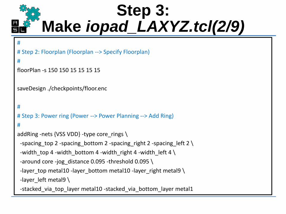
#
# Step 2: Floorplan (Floorplan --> Specify Floorplan)
#
floorPlan -s 150 150 15 15 15 15
saveDesign ./checkpoints/floor.enc
#
# Step 3: Power ring (Power --> Power Planning --> Add Ring)
#
addRing -nets {VSS VDD} -type core_rings \
-spacing_top 2 -spacing_bottom 2 -spacing_right 2 -spacing_left 2 \
-width_top 4 -width_bottom 4 -width_right 4 -width_left 4 \
-around core -jog_distance 0.095 -threshold 0.095 \
-layer_top metal10 -layer_bottom metal10 -layer_right metal9 \
-layer_left metal9 \
-stacked_via_top_layer metal10 -stacked_via_bottom_layer metal1

Step 3: Make iopad_LAXYZ.tcl(3/9)
#
# Step 4: Power stripe (Power --> Power Planning --> Add Striple)
#
addStripe -nets {VSS VDD} -layer metal8 -width 4 -spacing 2 \
-block_ring_top_layer_limit metal9 -block_ring_bottom_layer_limit metal7 \
-padcore_ring_top_layer_limit metal9 -padcore_ring_bottom_layer_limit metal7 \
-stacked_via_top_layer metal10 -stacked_via_bottom_layer metal1 \
-set_to_set_distance 50 -xleft_offset 50 -merge_stripes_value 0.095 \
-max_same_layer_jog_length 1.6

Step 3: Make iopad_LAXYZ.tcl(4/9)
#
# Step 5: Power route (Route --> Special Router)
#
globalNetConnect VDD -pin VDD -inst * -type pgpin
globalNetConnect VSS -pin VSS -inst * -type pgpin
sroute -nets {VSS VDD} -layerChangeRange {1 10} \
-connect { blockPin padPin padRing corePin floatingStripe } \
-blockPinTarget { nearestRingStripe nearestTarget } \
-padPinPortConnect { allPort oneGeom } \
-checkAlignedSecondaryPin 1 -blockPin useLef -allowJogging 1 \
-crossoverViaBottomLayer 1 -allowLayerChange 1 -targetViaTopLayer 10 \
-crossoverViaTopLayer 10 -targetViaBottomLayer 1
saveDesign ./checkpoints/power.enc

Step 3: Make iopad_LAXYZ.tcl(5/9)
#
# Step 6: Placement (Place --> Standard Cell)
#
placeDesign -prePlaceOpt
#
# Step 7: Optimization (preCTS) (Optimize --> Optimize Design)
#
optDesign -preCTS
#
# Step 8: Clock tree synthesis (CTS) (Clock --> Cynthesize Clock Tree)
#
addCTSCellList {CLKBUF_X1 CLKBUF_X2 CLKBUF_X3}
clockDesign -genSpecOnly Clock.ctstch
clockDesign -specFile Clock.ctstch -outDir clock_report -fixedInstBeforeCTS
saveDesign ./checkpoints/cts.enc

Step 3: Make iopad_LAXYZ.tcl(6/9)
#
# Step 9: Clock tree check (Clock --> Display --> Display Clock Tree)
#
#
# Step 9: Optimization (postCTS) (Optimize --> Optimize Design)
#
optDesign -postCTS
optDesign -postCTS -hold
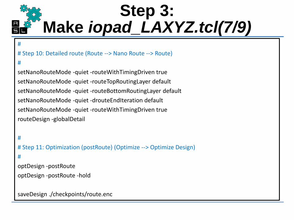
Step 3: Make iopad_LAXYZ.tcl(7/9)
#
# Step 10: Detailed route (Route --> Nano Route --> Route)
#
setNanoRouteMode -quiet -routeWithTimingDriven true
setNanoRouteMode -quiet -routeTopRoutingLayer default
setNanoRouteMode -quiet -routeBottomRoutingLayer default
setNanoRouteMode -quiet -drouteEndIteration default
setNanoRouteMode -quiet -routeWithTimingDriven true
routeDesign -globalDetail
#
# Step 11: Optimization (postRoute) (Optimize --> Optimize Design)
#
optDesign -postRoute
optDesign -postRoute -hold
saveDesign ./checkpoints/route.enc

Step 3: Make iopad_LAXYZ.tcl(8/9)
#
# Step 12: Add fillers (Place --> Physical Cells --> Add Filler)
#
addFiller -prefix FILLER -cell FILLCELL_X1 FILLCELL_X2 FILLCELL_X4 \
FILLCELL_X8 FILLCELL_X16 FILLCELL_X32
#
# Step 13: Verification (LVS) (Verify --> Verify Connectivity)
#
verifyConnectivity -type all -error 1000 -warning 50
#
# Step 14: Verification (DRC) (Verify --> Verify Geometry)
#
verifyGeometry

Step 3: Make iopad_LAXYZ.tcl(9/9)
#
# Step 15: Data out (Timing --> Extract RC, Timing --> Write SDF,
# File --> Save --> Netlist)
saveNetlist ./output/router_LAXYZ.vnet
isExtractRCModeSignoff
rcOut -spef ./output/router_LAXYZ.spef
delayCal -sdf ./output/router_LAXYZ.sdf -idealclock
saveDesign ./checkpoints/final.enc

Step 4:Script execution
Type velocity –init script/iopad_LAXYZ.tcl to start execute the script
%velocity script/par_LAXYZ.tcl
Type win to start SoC Encounter and visualize the final layout
%velocity script/par_LAXYZ.tcl

Final Layout
Your final Chip layout will appear on the main window. Congratulations!

Final Layout
• If we zoom in, we can see the connection established between the pin, the pad and the signals wires connected to the input-ports
• This figure shows the pads insertion for VDD, VSS, and the local input-port (data-in 0~11)
Pin
Pad

ACKNOWLEDGEMENT
• THIS WORK IS SUPPORTED BY VLSI DESIGN AND EDUCATION CENTER (VDEC), THE UNIVERSITY OF TOKYO, JAPAN, IN COLLABORATION WITH SYNOPSYS, Inc. and CADENCE DESIGN SYSTEMS, Inc.
• THIS WORK IS SUPPORTED BY COMPETITIVE RESEARCH FUNDING, UNIVERSITY OF AIZU, JAPAN, Ref. P12-2013.
187
<== Back to Contents