nxp semiconductors. document number: an12270 application ... · sd/emmc: mmc write 80000000 8 800...
TRANSCRIPT

© 2019 NXP B.V.
NXP Semiconductors. Document Number: AN12270
Application Notes Rev. 0 , 01/2019

Bringing up Layerscape devices using CCS script and DRAM boot, Application Notes, Rev. 0, 01/2019
2 NXP Semiconductors
Bringing up Layerscape devices using
CCS script and DRAM boot
1. Introduction
After the power is turned on, the Layerscape (LS) device
starts the booting process. It fetches RCW (Reset
Configuration Word) from the boot source specified with the
configuration pins cfg_rcw_src. If the flash memory that
stores the boot image is blank, RCW is invalid. The LS
devices’ boot logic first checks the format of RCW; when it
does not see a valid header, the booting process is stalled.
If the boot source is removable, such as an SD card, then the
SD card can be programmed with either a PC, or with other
boards.
For the boot flash, such as SPI flash/NOR flash/NAND
flash/eMMC, which is typically soldered on the board,
following are two common ways to program the boot image:
1. If possible, modify the cfg_rcw_src pin strapping
to select a valid hard coded RCW option, as specified
in the Reference Manual. This will put the device in a
good state. Then, use the flash programming tools of
the users’ choice to program the flash.
2. Use NXP CodeWarrior flash programming tool.
CodeWarrior tool implements a method to override
RCW, even when flash is blank. CW forces a hard
coded RCW into the device without relying on
switches and proceeds to program the flash device.
There is a 3rd less common way to program the flash:
3. Using a JTAG/BSDL flash programming tool, such
as Asset.
This application note describes a new method to bring up a
Layerscape board.
Contents
1. Introduction ........................................................................ 2 2. Description of the method .................................................. 3 3. Description of CCS scripts ................................................. 6 4. Validation summary ........................................................... 8 5. Useful information ........................................................... 10 Appendix A. Scripts ............................................................ 12
A.1. lsbp.tcl ................................................................... 12 A.2. ddr-init-ls1021twr.tcl ............................................ 16 A.3. ddr-init-ls1043rdb.tcl ............................................ 18 A.4. ddr-init-ls1046rdb.tcl ............................................ 20
Appendix B. Revision History ............................................ 23

Bringing up Layerscape devices using CCS script and DRAM boot, Application Notes, Rev. 0, 01/2019
NXP Semiconductors 3
2. Description of the method
Note: Users must ensure that the RESET_REQ signal does not generate HRESET_B or PORESET_B
signals in order for this method to work.
CodeWarrior comes with a low-level scripting tool CCS (CodeWarrior Communication Server). CCS
uses commands, as well as a series of commands in TCL script to control and communicate with the
boards.
A TCL script named lsbp.tcl is developed to simplify and automate the bring-up process. The full
script is provided in Appendix A for the purpose of information and reference. The script only needs a
few customizations to start the bring up process for a new board.
This method requires that U-Boot image be loaded into DDR via JTAG, and thus depends on a working
DDR.
The lsbp.tcl script calls the DDR init script that is used to configure and initialize the DDR
controller registers.
Note: The user should utilize the QCVS DDR tool to obtain the correct DDR controller register
values for the board. For a specific hard code RCW used in lsbp.tcl, there is a fixed DDR clock
ratio, which cannot be overridden/changed. Be sure to use the correct DDR speed in the QCVS tool
to generate working DDR register settings.
If the DDR is working and boot image can be reliably loaded to DDR, we can typically expect to view
some output on the console port. Users should proceed to debug the U-Boot until it boots successfully to
the command prompt.
Followings are the steps to bring up a new board:
1) Customize lsbp.tcl.
More information is in the Section 3, "Description of the CCS scripts".
2) Customize DDR init file.
An example DDR init file is provided as template for each supported device in Appendix A.
Users need to modify the DDR register setting based on DDR design of their boards.
3) Install CodeWarrior.
Download CodeWarrior for QorIQ LS series Armv8 ISA from NXP website.
CCS executable can be found, in
{installation directory\Common\CCS\bin}.
For example,
C:\Freescale\CW4NET_v2018.01\Common\CCS\bin
4) Copy all the TCL scripts and u-boot.bin to the CCS directory.
5) Launch CCS.
Double click ccs.exe.

Description of the method
Bringing up Layerscape devices using CCS script and DRAM boot, Application Notes, Rev. 0, 01/2019
4 NXP Semiconductors
Figure 1: CCS icon in the System Tray
6) In CCS windows, run the lspb.tcl script.
Figure 2: Output after running the lsbp.tcl script
Once U-Boot from DRAM boot is successful, the flash image can be burned to the flash with U-Boot
command. Then the board can boot from the flash, without JTAG’s involvement. In the beginning of the
board bring-up, it is possible that network interface is not working yet. So TFTP cannot be used to
Double click the CCS icon in the
bottom right System Tray.
Bringing up Layerscape devices using CCS script and DRAM boot, Application Notes, Rev. 0, 01/2019
NXP Semiconductors 5
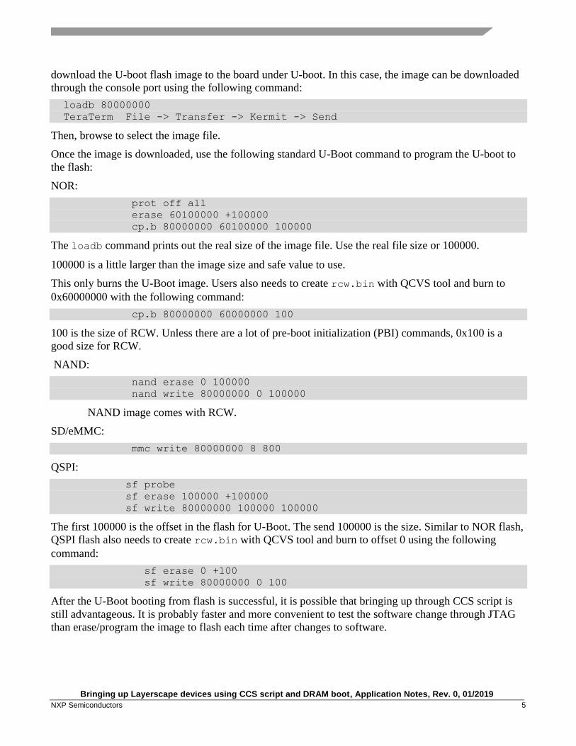
download the U-boot flash image to the board under U-boot. In this case, the image can be downloaded
through the console port using the following command:
loadb 80000000
TeraTerm File -> Transfer -> Kermit -> Send
Then, browse to select the image file.
Once the image is downloaded, use the following standard U-Boot command to program the U-boot to
the flash:
NOR:
prot off all
erase 60100000 +100000
cp.b 80000000 60100000 100000
The loadb command prints out the real size of the image file. Use the real file size or 100000.
100000 is a little larger than the image size and safe value to use.
This only burns the U-Boot image. Users also needs to create rcw.bin with QCVS tool and burn to
0x60000000 with the following command:
cp.b 80000000 60000000 100
100 is the size of RCW. Unless there are a lot of pre-boot initialization (PBI) commands, 0x100 is a
good size for RCW.
NAND:
nand erase 0 100000
nand write 80000000 0 100000
NAND image comes with RCW.
SD/eMMC:
mmc write 80000000 8 800
QSPI:
sf probe
sf erase 100000 +100000
sf write 80000000 100000 100000
The first 100000 is the offset in the flash for U-Boot. The send 100000 is the size. Similar to NOR flash,
QSPI flash also needs to create rcw.bin with QCVS tool and burn to offset 0 using the following
command:
sf erase 0 +100
sf write 80000000 0 100
After the U-Boot booting from flash is successful, it is possible that bringing up through CCS script is
still advantageous. It is probably faster and more convenient to test the software change through JTAG
than erase/program the image to flash each time after changes to software.

Description of CCS scripts
Bringing up Layerscape devices using CCS script and DRAM boot, Application Notes, Rev. 0, 01/2019
6 NXP Semiconductors
3. Description of CCS scripts
lsbp.tcl is the main script that automates the following steps:
• RCW override
• JTAG parsing to find out Boot Core/SAP2/DAP chain position
• PBI to initialize some minimal required registers
• Configure DDR
• Load boot loader(U-boot) image to DDR
• Release the ARM core to boot.
The lsbp.tcl script makes use of the following two files:
• ddr-init-lsxxxxxxx.tcl to initialize DDR controller
• u-boot.bin is the U-boot DRAM image
Users can use a different name as long as the file name in the script matches the real file name.
Following is the main part of the script:
lsbp.tcl
#1: Customize the ddr init script file name
source ddr-init-ls10xxxxx.tcl
#2: Set device, currently supports ls1021a/ls1043a/ls1046a
set device ls1043a
switch -exact $device {
"ls1021a" { set dut ls1020a }
"ls1043a" { set dut ls1043a }
"ls1046a" { set dut ls1043a }
default {echo This device is not supported; return 0}
}
#3: Set hardcode_rcw
# For LS1043A and LS1046A
# 0x9E: DDRCLK is the reference clock for DDR
# 0x9F: DIFF_SYSCLK is the reference clock for DDR
# For LS1021A
# 0x9B: First try value. See RM for more options
set hardcode_rcw 0x9E
#4: Customize the CWTAP setting, see the lsbp.tcl script in Appendix for
more info
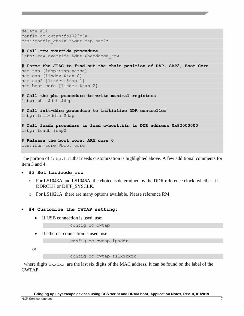
Bringing up Layerscape devices using CCS script and DRAM boot, Application Notes, Rev. 0, 01/2019
NXP Semiconductors 7
delete all
config cc cwtap:fsl023b3a
ccs::config_chain "$dut dap sap2"
# Call rcw-override procedure
lsbp::rcw-override $dut $hardcode_rcw
# Parse the JTAG to find out the chain position of DAP, SAP2, Boot Core
set tap [lsbp::tap-parse]
set dap [lindex $tap 0]
set sap2 [lindex $tap 1]
set boot_core [lindex $tap 2]
# Call the pbi procedure to write minimal registers
lsbp::pbi $dut $dap
# Call init-ddrc procedure to initialize DDR controller
lsbp::init-ddrc $dap
# Call loadb procedure to load u-boot.bin to DDR address 0x82000000
lsbp::loadb $sap2
# Release the boot core, ARM core 0
ccs::run_core $boot_core
}
The portion of lsbp.tcl that needs customization is highlighted above. A few additional comments for
item 3 and 4:
• #3 Set hardcode_rcw
o For LS1043A and LS1046A, the choice is determined by the DDR reference clock, whether it is
DDRCLK or DIFF_SYSCLK.
o For LS1021A, there are many options available. Please reference RM.
• #4 Customize the CWTAP setting:
• If USB connection is used, use:
config cc cwtap
• If ethernet connection is used, use:
config cc cwtap:ipaddr
or
config cc cwtap:fslxxxxxx
where digits xxxxxx are the last six digits of the MAC address. It can be found on the label of the
CWTAP.

Validation summary
Bringing up Layerscape devices using CCS script and DRAM boot, Application Notes, Rev. 0, 01/2019
8 NXP Semiconductors
Figure 3: Last six digits of the MAC address as found on CWTAP label
4. Validation summary
All the validation has been performed with the U-Boot using LSDK 18.06. Currently this script supports
LS1021A, LS1043A, and LS1046A. More devices may be supported in the future.
NOTE: In general, U-boot compilation target for DRAM boot is different from target for booting
from flash.
For booting from NOR/QSPI flash, NOR/QSPI is memory mapped and supports in-place execution. The
boot flow is that the core starts execution from the flash, the boot code configures DDR controller, it
then copies the U-Boot image from the flash to the DRAM and finally jumps to the code in the DRAM
to complete the U-Boot.
For booting from SD/eMMC/NAND, those interfaces are not memory mapped and do not support
in-place execution. A feature called PBI (Pre-Boot Loader Initializer) is utilized to copy a small program
SPL (Secondary Program Loader) to OCRAM. The boot starts with SPL residing in OCRAM. SPL
configures DDR controller and then jumps to code in DRAM to completes the U-Boot. For
SD/eMMC/NAND, the compiler generates two binary images, one is u-boot.bin, which is the
DRAM version of U-Boot that does not try to initialize DDR. The other is u-boot-with-spl-
pbl.bin, this image combines u-boot, PBL, and SPL to a single image.
For DRAM booting, u-boot.bin from compilation target SD/eMMC or NAND is always used even
for NOR/QSPI booting.
For example, for LS1043A NOR, the target for DRAM boot is ls1043ardb_sdcard_defconfig,
while target for NOR flash boot is ls1043ardb_defconfig.
The image name for DRAM boot is always u-boot.bin. For flash booting, the name might be
different, either u-boot.bin or u-boot-with-spl-pbl.bin.
fsl023b3a

Bringing up Layerscape devices using CCS script and DRAM boot, Application Notes, Rev. 0, 01/2019
NXP Semiconductors 9
Table 1: NXP Boards and their test summary
Device Board Boot
Source
U-Boot compilation
target image for
DRAM boot
U-Boot compilation
target image for
flash boot
Note
LS1021A LS1021A
Tower
Board
NOR ls1021atwr_sdcard_ifc_
defconfig
u-boot.bin
ls1021atwr_nor_defconfig
u-boot.bin
DRAM boot tested
Flash boot tested
NAND NAND not supported
on Tower board. Even
cfg_rcw_src cannot be
set to NAND.
NAND not supported on
Tower board
Not supported on Tower
Board.
ls1021aqds_nand_defconfig
can be used as reference
target for both DRAM boot
and flash boot. The files,
u-boot.bin and u-boot-with-spl-
pbl.bin are the images for
RAM boot and NAND boot
QSPI ls1021atwr_sdcard_qspi
_defconfig
u-boot.bin
ls1021atwr_qspi_defconfig
u-boot.bin
DRAM boot tested
Flash boot tested
SD ls1021atwr_sdcard_ifc_
defconfig
u-boot.bin
ls1021atwr_sdcard_ifc_defconfig
u-boot-with-spl-pbl.bin
DRAM boot tested
Flash boot tested
LS1043A
LS1043
AR DB
NOR ls1043ardb_sdcard_defc
onfig u-boot.bin
ls1043ardb_defconfig
u-boot.bin
DRAM boot tested
Flash boot tested
NAN
D
ls1043ardb_nand_defc
onfig u-boot.bin
ls1043ardb_nand_defconfig u-boot-with-spl-pbl.bin
DRAM boot tested
Flash boot tested
SD ls1043ardb_sdcard_defc
onfig u-boot.bin
ls1043ardb_sdcard_defconfig u-boot-with-spl-pbl.bin
DRAM boot tested
Flash boot tested
QSPI ls1043ardb_sdcard_defc
onfig
u-boot.bin
LS1043ARDB and LSDK
18.06
does not support QSPI flash.
User can use
ls1043aqds_qspi_defco nfig as
reference target. u-boot.bin
should be programmed
to QSPI flash.
DRAM boot tested
LS1046A
LS1046
AR DB
SD ls1046ardb_sdcard_defc
onfig u-boot.bin
ls1046ardb_sdcard_defconfig u-boot-with-spl-pbl.bin
DRAM boot tested
Flash boot tested
QSPI ls1046ardb_sdcard_defc
onfig u-boot.bin
ls1046ardb_qspi_defconfig u-boot.bin
DRAM boot tested
Flash boot tested
NOR ls1046ardb_sdcard_defc
onfig
u-boot.bin
LS1046ARDB and LSDK
18.06
does not support NOR flash.
User can use
DRAM boot tested

Useful information
Bringing up Layerscape devices using CCS script and DRAM boot, Application Notes, Rev. 0, 01/2019
10 NXP Semiconductors
Device Board Boot
Source
U-Boot compilation
target image for
DRAM boot
U-Boot compilation
target image for
flash boot
Note
ls1046aqds_defconf
ig as reference target.
u-boot.bin should be
programmed to NOR
flash.
5. Useful information
1. Currently in rcw-override procedure, only rcw11 is overridden with the following
CCS command:
ccs::write_reg 0 rcw11 0x00030000
If desirable, other RCW words can be overridden as well by adding new override
commands in this procedure. Note that rcw index from 0 to 15 in the TCL script.
Note: Users must take care that the PLL ratio is not overridden/changed. It
always uses the ratio documented in the RM. If PLL override is added
here, override will not take effect in PLL circuit, although RCWSR1-16
from DCFG is changed.
2. For all possible hardcode RCW options:
• LS1043A DDR always runs at 13:1 ratio.
• LS1046A DDR always runs at 16:1 ratio.
• LS1021A has more clocking options.
DDR controller register values obtained using QCVS should take into account that
the DDR clock speed is as shown above, and it cannot be changed with RCW
override.
3. In order to test if the JTAG interface is working or not, in the CCS windows, use the
following command:
source IDcode.tcl
If JTAG interface works, it should display the Layerscape device ID.
4. In the end of rcw_override, it displays the JTAG chain information. If it only shows
Chain Position 0: LSxxxxA
Chain Position 1: DAP
Chain Position 2: SAP2
This means the override fails. If it succeeds, it should show a lot more chain positions, including all
the ARM cores. Following are the last chain if override succeeds.
LS1021A: Chain Position 18: SAP2

Bringing up Layerscape devices using CCS script and DRAM boot, Application Notes, Rev. 0, 01/2019
NXP Semiconductors 11
LS1043A: Chain Position 33: SAP2
LS1046A: Chain Position 33: SAP2
5. In order to test if DDR is working, you can comment out the following two lines from lsbp.tcl:
#lsbp::loadb $sap2
#ccs::run_core $boot_core
Then lsbp.tcl initializes the DDR controller without loading u-boot image to DDR and releases
the ARM core.
Use following command to read write to memory. 18 is SAP2 for LS1021A. For
LS1043A/LS1046A, replace 18 with 33.
(bin) 80 % ccs::write_mem 18 0 0x82000000 4 0 {0x1 0x2 0x3 0x4}
(bin) 81 % disp ccs::read_mem 18 0 0x82000000 4 0 8
+0 +4 +8 +C
[0x0000000082000000] 00000001 00000002 00000003 00000004
[0x0000000082000010] E59FF014 E59FF014 E59FF014 E59FF014
(bin) 82 % disp ccs::read_mem 18(or 33) 0 0x1080000 4 0 0x400 #display all
DDR registers.
6. Some additional CCS commands for debugging:
a) The following two lines reads PC. Use 9 in place of chain_position_for_first_core for
LS1021A. 16 is for LS1043A and LS1046A. A core has to be stopped before read.
ccs::stop_core chain_position_for_first_core
disp ccs::read_reg chain_position_for_first_core pc 1
b) The following line steps one instructions. You can use greater number in place of 1 to run #
multiple instructions.
ccs::step_core chain_position_for_first_core 1

Useful information
Bringing up Layerscape devices using CCS script and DRAM boot, Application Notes, Rev. 0, 01/2019
12 NXP Semiconductors
Appendix A. Scripts
A.1. lsbp.tcl
namespace eval lsbp {
proc lsbp {} {
#1: Customize the ddr init script file name
source ddr-init-ls10xxxxx.tcl
#2: Set device, currently supports ls1021a/ls1043a/ls1046a
set device ls1021a
switch -exact $device {
"ls1021a" { set dut ls1020a }
"ls1043a" { set dut ls1043a }
"ls1046a" { set dut ls1043a }
default {echo This device is not supported; return 0}
}
#3: Set hardcode_rcw
# For LS1043A and LS1046A
# 0x9E: DDRCLK is the reference clock for DDR
# 0x9F: DIFF_SYSCLK is the reference clock for DDR
# For LS1021A
# 0x9B: First try value. See RM for more options
set hardcode_rcw 0x9B
#4: Please customize the CWTAP setting, see Apps note for more info
delete all
config cc cwtap:fsl023b3a
ccs::config_chain "$dut dap sap2"
# Call rcw-override procedure
lsbp::rcw-override $dut $hardcode_rcw
# Parse the JTAG to find out the chain position of DAP, SAP2, Boot Core
set tap [lsbp::tap-parse]
set dap [lindex $tap 0]
set sap2 [lindex $tap 1]
set boot_core [lindex $tap 2]
# Call the pbi procedure to write minimal registers
lsbp::pbi $dut $dap
# Call init-ddrc procedure to initialize DDR controller
lsbp::init-ddrc $dap
# Call loadb procedure to load u-boot.bin to DDR address 0x82000000
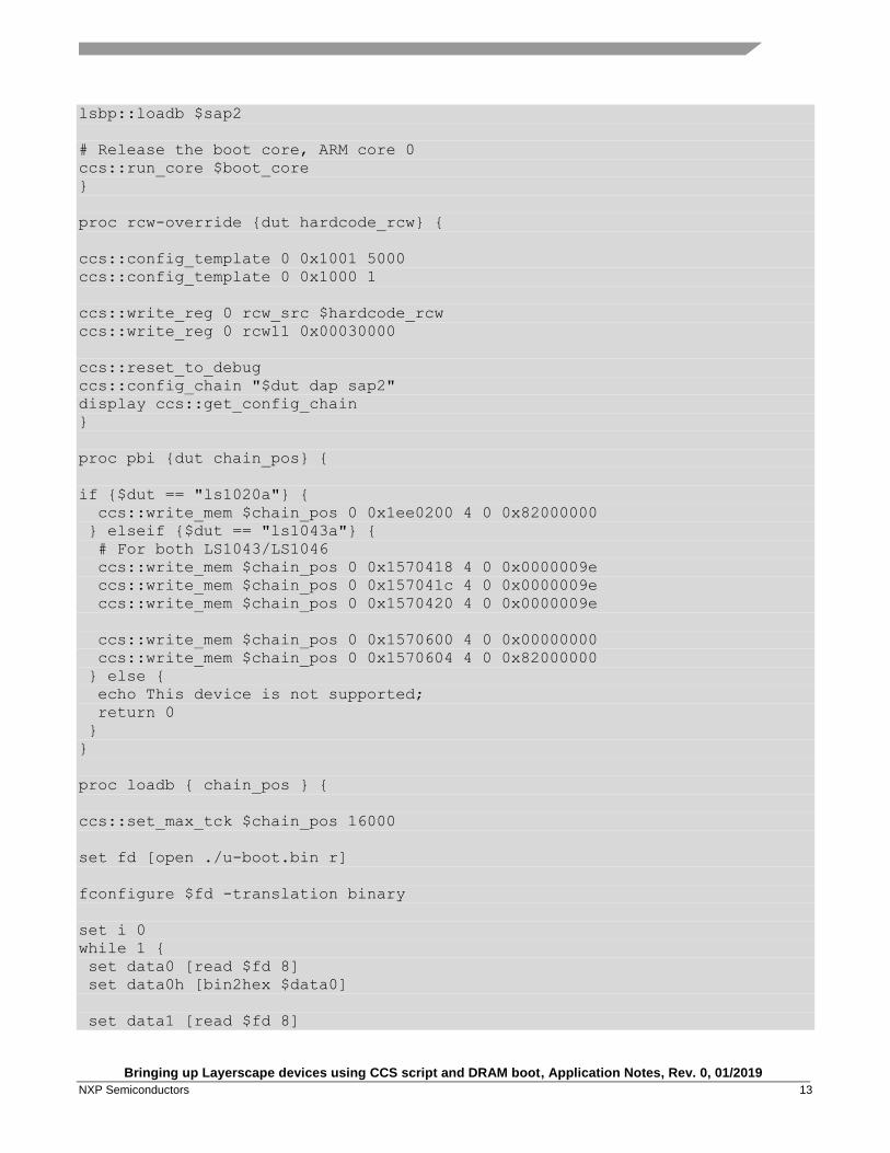
Bringing up Layerscape devices using CCS script and DRAM boot, Application Notes, Rev. 0, 01/2019
NXP Semiconductors 13
lsbp::loadb $sap2
# Release the boot core, ARM core 0
ccs::run_core $boot_core
}
proc rcw-override {dut hardcode_rcw} {
ccs::config_template 0 0x1001 5000
ccs::config_template 0 0x1000 1
ccs::write_reg 0 rcw_src $hardcode_rcw
ccs::write_reg 0 rcw11 0x00030000
ccs::reset_to_debug
ccs::config_chain "$dut dap sap2"
display ccs::get_config_chain
}
proc pbi {dut chain_pos} {
if {$dut == "ls1020a"} {
ccs::write_mem $chain_pos 0 0x1ee0200 4 0 0x82000000
} elseif {$dut == "ls1043a"} {
# For both LS1043/LS1046
ccs::write_mem $chain_pos 0 0x1570418 4 0 0x0000009e
ccs::write_mem $chain_pos 0 0x157041c 4 0 0x0000009e
ccs::write_mem $chain_pos 0 0x1570420 4 0 0x0000009e
ccs::write_mem $chain_pos 0 0x1570600 4 0 0x00000000
ccs::write_mem $chain_pos 0 0x1570604 4 0 0x82000000
} else {
echo This device is not supported;
return 0
}
}
proc loadb { chain_pos } {
ccs::set_max_tck $chain_pos 16000
set fd [open ./u-boot.bin r]
fconfigure $fd -translation binary
set i 0
while 1 {
set data0 [read $fd 8]
set data0h [bin2hex $data0]
set data1 [read $fd 8]
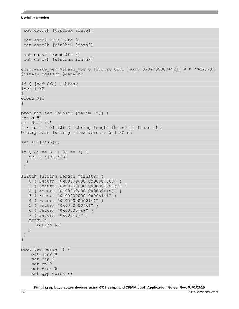
Useful information
Bringing up Layerscape devices using CCS script and DRAM boot, Application Notes, Rev. 0, 01/2019
14 NXP Semiconductors
set data1h [bin2hex $data1]
set data2 [read $fd 8]
set data2h [bin2hex $data2]
set data3 [read $fd 8]
set data3h [bin2hex $data3]
ccs::write_mem $chain_pos 0 [format 0x%x [expr 0x82000000+$i]] 8 0 "$data0h
$data1h $data2h $data3h"
if { [eof $fd] } break
incr i 32
}
close $fd
}
proc bin2hex {binstr {delim ""}} {
set s ""
set 0x " 0x"
for {set i 0} {$i < [string length $binstr]} {incr i} {
binary scan [string index $binstr $i] H2 cc
set s ${cc}${s}
if { $i == 3 || $i == 7} {
set s ${0x}${s}
}
}
switch [string length $binstr] {
0 { return "0x00000000 0x00000000" }
1 { return "0x00000000 0x000000${s}" }
2 { return "0x00000000 0x0000${s}" }
3 { return "0x00000000 0x00${s}" }
4 { return "0x00000000${s}" }
5 { return "0x000000${s}" }
6 { return "0x0000${s}" }
7 { return "0x00${s}" }
default {
return $s
}
}
}
proc tap-parse {} {
set sap2 0
set dap 0
set sp 0
set dpaa 0
set gpp_cores {}

Bringing up Layerscape devices using CCS script and DRAM boot, Application Notes, Rev. 0, 01/2019
NXP Semiconductors 15
set chain_pos 0
set children [ccs::get_config_chain]
set tap_num 0
foreach child $children {
set type $child
#echo $type
if {$type == $ccs::core(sap2)} { set sap2 $tap_num
} elseif {$type == $ccs::core(dap)} { set dap $tap_num
} elseif {$type == $ccs::core(CortexA5)} { set sp $tap_num
} elseif {$type == $ccs::core(lsdpaa2)} { set dpaa $tap_num
} elseif {$type == $ccs::core(CortexA53)} { lappend gpp_cores
$tap_num
} elseif {$type == $ccs::core(CortexA72)} { lappend gpp_cores
$tap_num
} elseif {$type == $ccs::core(CortexA7)} { lappend gpp_cores
$tap_num }
incr tap_num
}
set boot_core [lindex $gpp_cores 0]
return [list $dap $sap2 $boot_core]
}
}

Useful information
Bringing up Layerscape devices using CCS script and DRAM boot, Application Notes, Rev. 0, 01/2019
16 NXP Semiconductors
A.2. ddr-init-ls1021twr.tcl
namespace eval lsbp {
###################################################################
# DDR Initialization
###################################################################
proc init-ddrc { chain_pos } {
#CCI-400
#ccs::write_mem $chain_pos 0 0x1185000 4 0 0x00000003
# 1600 MHz
# sdram_cfg
ccs::write_mem $chain_pos 0 0x01080110 4 0 0x470c0008
# cs0_bnds
ccs::write_mem $chain_pos 0 0x01080000 4 0 0x008000bf
# cs1_bnds
ccs::write_mem $chain_pos 0 0x01080008 4 0 0x00000000
# cs0_config
ccs::write_mem $chain_pos 0 0x01080080 4 0 0x80014302
# cs1_config
ccs::write_mem $chain_pos 0 0x01080084 4 0 0x00000000
# timing_cfg_3
ccs::write_mem $chain_pos 0 0x01080100 4 0 0x010e1000
# timing_cfg_0
ccs::write_mem $chain_pos 0 0x01080104 4 0 0x50550004
# timing_cfg_1
ccs::write_mem $chain_pos 0 0x01080108 4 0 0xbcb38c56
# timing_cfg_2
ccs::write_mem $chain_pos 0 0x0108010C 4 0 0x0040d120
# timing_cfg_4
ccs::write_mem $chain_pos 0 0x01080160 4 0 0x00000001
# timing_cfg_5
ccs::write_mem $chain_pos 0 0x01080164 4 0 0x03401400
# sdram_cfg_2
ccs::write_mem $chain_pos 0 0x01080114 4 0 0x00401010
# sdram_mode
ccs::write_mem $chain_pos 0 0x01080118 4 0 0x00061c60
# sdram_mode_2
ccs::write_mem $chain_pos 0 0x0108011C 4 0 0x00180000
# sdram_interval
ccs::write_mem $chain_pos 0 0x01080124 4 0 0x18600618
# ddr_wrlvl_cntl
ccs::write_mem $chain_pos 0 0x01080174 4 0 0xc655f605
# ddr_wrlvl_cntl_2
ccs::write_mem $chain_pos 0 0x01080190 4 0 0x05060607
# ddr_wrlvl_cntl_3
ccs::write_mem $chain_pos 0 0x01080194 4 0 0x05050505
# ddr_cdr1
ccs::write_mem $chain_pos 0 0x01080B28 4 0 0x80040000

Bringing up Layerscape devices using CCS script and DRAM boot, Application Notes, Rev. 0, 01/2019
NXP Semiconductors 17
# ddr_cdr2
ccs::write_mem $chain_pos 0 0x01080B2C 4 0 0x00000001
# sdram_clk_cntl
ccs::write_mem $chain_pos 0 0x01080130 4 0 0x02000000
# ddr_zq_cntl
ccs::write_mem $chain_pos 0 0x01080170 4 0 0x89080600
# cs0_config_2
ccs::write_mem $chain_pos 0 0x010800C0 4 0 0x00000000
# data_init
ccs::write_mem $chain_pos 0 0x01080128 4 0 0xDEADBEEF
after 1000
# sdram_cfg
ccs::write_mem $chain_pos 0 0x01080110 4 0 0xc70c0008
}
}
Useful information
Bringing up Layerscape devices using CCS script and DRAM boot, Application Notes, Rev. 0, 01/2019
18 NXP Semiconductors
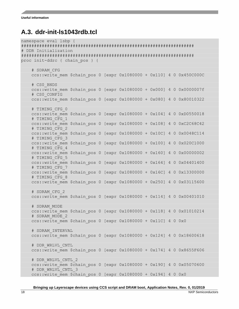
A.3. ddr-init-ls1043rdb.tcl
namespace eval lsbp {
###################################################################
# DDR Initialization
###################################################################
proc init-ddrc { chain_pos } {
# SDRAM_CFG
ccs::write_mem $chain_pos 0 [expr 0x1080000 + 0x110] 4 0 0x450C000C
# CS0_BNDS
ccs::write_mem $chain_pos 0 [expr 0x1080000 + 0x000] 4 0 0x0000007f
# CS0_CONFIG
ccs::write_mem $chain_pos 0 [expr 0x1080000 + 0x080] 4 0 0x80010322
# TIMING_CFG_0
ccs::write_mem $chain_pos 0 [expr 0x1080000 + 0x104] 4 0 0xD0550018
# TIMING_CFG_1
ccs::write_mem $chain_pos 0 [expr 0x1080000 + 0x108] 4 0 0xC2C68C42
# TIMING_CFG_2
ccs::write_mem $chain_pos 0 [expr 0x1080000 + 0x10C] 4 0 0x0048C114
# TIMING_CFG_3
ccs::write_mem $chain_pos 0 [expr 0x1080000 + 0x100] 4 0 0x020C1000
# TIMING_CFG_4
ccs::write_mem $chain_pos 0 [expr 0x1080000 + 0x160] 4 0 0x00000002
# TIMING_CFG_5
ccs::write_mem $chain_pos 0 [expr 0x1080000 + 0x164] 4 0 0x04401400
# TIMING_CFG_7
ccs::write_mem $chain_pos 0 [expr 0x1080000 + 0x16C] 4 0 0x13300000
# TIMING_CFG_8
ccs::write_mem $chain_pos 0 [expr 0x1080000 + 0x250] 4 0 0x03115600
# SDRAM_CFG_2
ccs::write_mem $chain_pos 0 [expr 0x1080000 + 0x114] 4 0 0x00401010
# SDRAM_MODE
ccs::write_mem $chain_pos 0 [expr 0x1080000 + 0x118] 4 0 0x01010214
# SDRAM_MODE_2
ccs::write_mem $chain_pos 0 [expr 0x1080000 + 0x11C] 4 0 0x0
# SDRAM_INTERVAL
ccs::write_mem $chain_pos 0 [expr 0x1080000 + 0x124] 4 0 0x18600618
# DDR_WRLVL_CNTL
ccs::write_mem $chain_pos 0 [expr 0x1080000 + 0x174] 4 0 0x8655F606
# DDR_WRLVL_CNTL_2
ccs::write_mem $chain_pos 0 [expr 0x1080000 + 0x190] 4 0 0x05070600
# DDR_WRLVL_CNTL_3
ccs::write_mem $chain_pos 0 [expr 0x1080000 + 0x194] 4 0 0x0

Bringing up Layerscape devices using CCS script and DRAM boot, Application Notes, Rev. 0, 01/2019
NXP Semiconductors 19
# DDR_CDR1
ccs::write_mem $chain_pos 0 [expr 0x1080000 + 0xB28] 4 0 0x80040000
# DDR_CDR2
ccs::write_mem $chain_pos 0 [expr 0x1080000 + 0xB2C] 4 0 0x0000A181
# SDRAM_CLK_CNTL
ccs::write_mem $chain_pos 0 [expr 0x1080000 + 0x130] 4 0 0x02000000
# DDR_ZQ_CNTL
ccs::write_mem $chain_pos 0 [expr 0x1080000 + 0x170] 4 0 0x8A090705
# SDRAM_MODE_9
ccs::write_mem $chain_pos 0 [expr 0x1080000 + 0x220] 4 0 0x00000400
# SDRAM_MODE_10
ccs::write_mem $chain_pos 0 [expr 0x1080000 + 0x224] 4 0 0x04000000
# CS0_CONFIG_2
ccs::write_mem $chain_pos 0 [expr 0x1080000 + 0x0C0] 4 0 0
# SDRAM_CFG
ccs::write_mem $chain_pos 0 [expr 0x1080000 + 0x110] 4 0 0xC50C000C
after 1000
}
}

Useful information
Bringing up Layerscape devices using CCS script and DRAM boot, Application Notes, Rev. 0, 01/2019
20 NXP Semiconductors
A.4. ddr-init-ls1046rdb.tcl
namespace eval lsbp {
###################################################################
# DDR Initialization
###################################################################
proc init-ddrc {chain_pos} {
# CS0_BNDS
ccs::write_mem $chain_pos 0 [expr 0x1080000 + 0x000] 4 0 0x000001ff
# CS0_CONFIG
ccs::write_mem $chain_pos 0 [expr 0x1080000 + 0x080] 4 0 0x80040322
# CS0_CONFIG_2
ccs::write_mem $chain_pos 0 [expr 0x1080000 + 0x0c0] 4 0 0x0
# CS_1_BNDS
ccs::write_mem $chain_pos 0 [expr 0x1080000 + 0x008] 4 0 0x000001ff
# CS1_CONFIG
ccs::write_mem $chain_pos 0 [expr 0x1080000 + 0x084] 4 0 0x80000322
# CS1_CONFIG_2
ccs::write_mem $chain_pos 0 [expr 0x1080000 + 0x0c4] 4 0 0x0
# CS_2_BNDS
ccs::write_mem $chain_pos 0 [expr 0x1080000 + 0x010] 4 0 0x00000000
# CS1_CONFIG
ccs::write_mem $chain_pos 0 [expr 0x1080000 + 0x088] 4 0 0x00000000
# CS1_CONFIG_2
ccs::write_mem $chain_pos 0 [expr 0x1080000 + 0x0c8] 4 0 0x0
# CS_2_BNDS
ccs::write_mem $chain_pos 0 [expr 0x1080000 + 0x018] 4 0 0x00000000
# CS1_CONFIG
ccs::write_mem $chain_pos 0 [expr 0x1080000 + 0x08c] 4 0 0x00000000
# CS1_CONFIG_2
ccs::write_mem $chain_pos 0 [expr 0x1080000 + 0x0cc] 4 0 0x0
# 1600MT/s
# TIMING_CFG_0
ccs::write_mem $chain_pos 0 [expr 0x1080000 + 0x104] 4 0 0x91550018
# TIMING_CFG_3
ccs::write_mem $chain_pos 0 [expr 0x1080000 + 0x100] 4 0 0x010c1000
# TIMING_CFG_1
ccs::write_mem $chain_pos 0 [expr 0x1080000 + 0x108] 4 0 0xbab48c42
# TIMING_CFG_2
ccs::write_mem $chain_pos 0 [expr 0x1080000 + 0x10C] 4 0 0x0048c111
# DDR_CDR1
ccs::write_mem $chain_pos 0 [expr 0x1080000 + 0xB28] 4 0 0x80040000
# DDR_CDR2

Bringing up Layerscape devices using CCS script and DRAM boot, Application Notes, Rev. 0, 01/2019
NXP Semiconductors 21
ccs::write_mem $chain_pos 0 [expr 0x1080000 + 0xB2C] 4 0 0x000000C1
# SDRAM_CFG
ccs::write_mem $chain_pos 0 [expr 0x1080000 + 0x110] 4 0 0x65044000
# DDR_DATA_INIT
ccs::write_mem $chain_pos 0 [expr 0x1080000 + 0x128] 4 0 0xDEADBEEF
# SDRAM_CFG_2
ccs::write_mem $chain_pos 0 [expr 0x1080000 + 0x114] 4 0 0x00401111
# SDRAM_MODE
ccs::write_mem $chain_pos 0 [expr 0x1080000 + 0x118] 4 0 0x03010210
# SDRAM_MODE_3
ccs::write_mem $chain_pos 0 [expr 0x1080000 + 0x200] 4 0 0x00010210
# SDRAM_MODE_5
ccs::write_mem $chain_pos 0 [expr 0x1080000 + 0x208] 4 0 0x00010210
# SDRAM_MODE_7
ccs::write_mem $chain_pos 0 [expr 0x1080000 + 0x210] 4 0 0x00010210
# SDRAM_MODE_2
ccs::write_mem $chain_pos 0 [expr 0x1080000 + 0x11C] 4 0 0x00000000
# SDRAM_MODE_4
ccs::write_mem $chain_pos 0 [expr 0x1080000 + 0x204] 4 0 0x00000000
# SDRAM_MODE_6
ccs::write_mem $chain_pos 0 [expr 0x1080000 + 0x20C] 4 0 0x00000000
# SDRAM_MODE_8
ccs::write_mem $chain_pos 0 [expr 0x1080000 + 0x214] 4 0 0x00000000
# SDRAM_MODE_9
ccs::write_mem $chain_pos 0 [expr 0x1080000 + 0x220] 4 0 0x00000500
# SDRAM_MODE_11
ccs::write_mem $chain_pos 0 [expr 0x1080000 + 0x228] 4 0 0x00000400
# SDRAM_MODE_13
ccs::write_mem $chain_pos 0 [expr 0x1080000 + 0x230] 4 0 0x00000400
# SDRAM_MODE_15
ccs::write_mem $chain_pos 0 [expr 0x1080000 + 0x238] 4 0 0x00000400
# SDRAM_MODE_10
ccs::write_mem $chain_pos 0 [expr 0x1080000 + 0x224] 4 0 0x00400000
# SDRAM_MODE_12
ccs::write_mem $chain_pos 0 [expr 0x1080000 + 0x22C] 4 0 0x00400000
# SDRAM_MODE_14
ccs::write_mem $chain_pos 0 [expr 0x1080000 + 0x234] 4 0 0x00400000
# SDRAM_MODE_16
ccs::write_mem $chain_pos 0 [expr 0x1080000 + 0x23c] 4 0 0x00400000
# SDRAM_INTERVAL
ccs::write_mem $chain_pos 0 [expr 0x1080000 + 0x124] 4 0 0x18600000
# DDR_SDRAM_CLK_CNTL
ccs::write_mem $chain_pos 0 [expr 0x1080000 + 0x130] 4 0 0x02000000
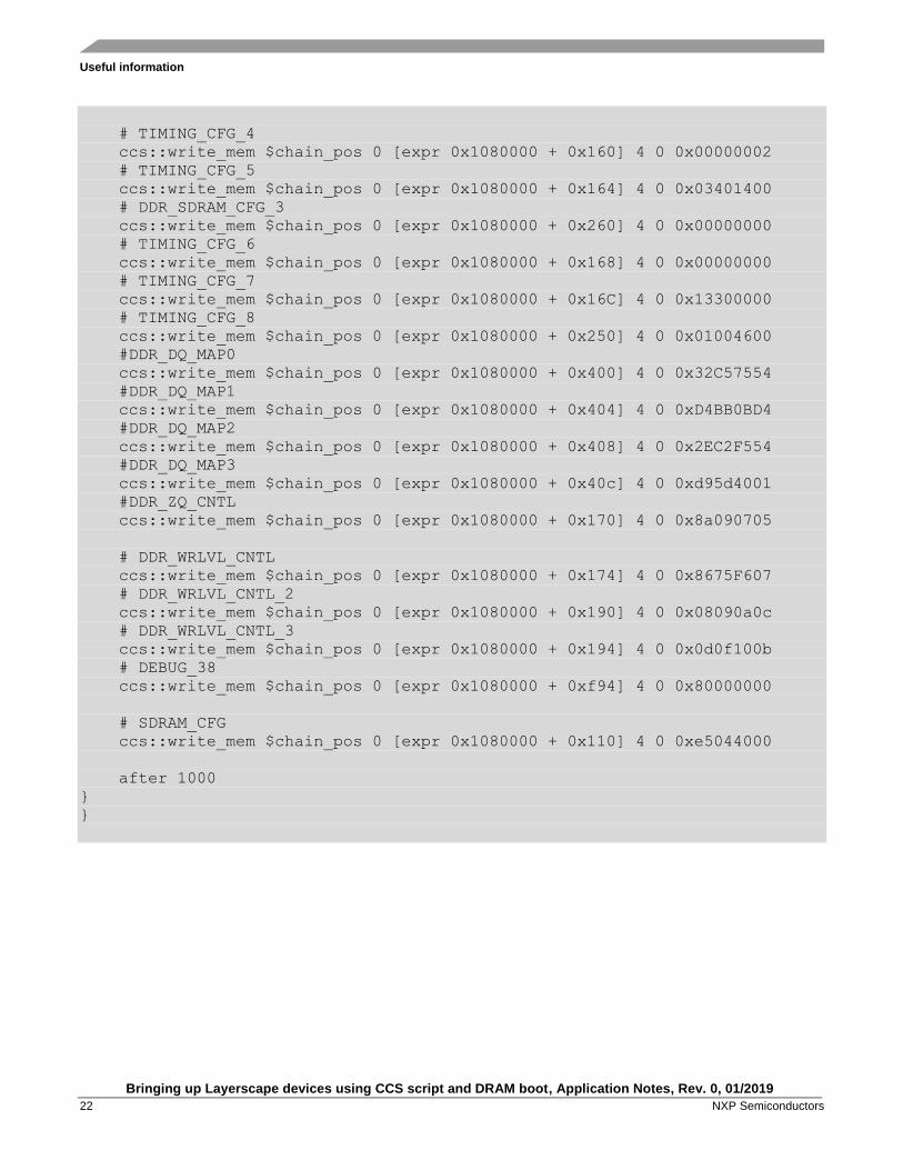
Useful information
Bringing up Layerscape devices using CCS script and DRAM boot, Application Notes, Rev. 0, 01/2019
22 NXP Semiconductors
# TIMING_CFG_4
ccs::write_mem $chain_pos 0 [expr 0x1080000 + 0x160] 4 0 0x00000002
# TIMING_CFG_5
ccs::write_mem $chain_pos 0 [expr 0x1080000 + 0x164] 4 0 0x03401400
# DDR_SDRAM_CFG_3
ccs::write_mem $chain_pos 0 [expr 0x1080000 + 0x260] 4 0 0x00000000
# TIMING_CFG_6
ccs::write_mem $chain_pos 0 [expr 0x1080000 + 0x168] 4 0 0x00000000
# TIMING_CFG_7
ccs::write_mem $chain_pos 0 [expr 0x1080000 + 0x16C] 4 0 0x13300000
# TIMING_CFG_8
ccs::write_mem $chain_pos 0 [expr 0x1080000 + 0x250] 4 0 0x01004600
#DDR_DQ_MAP0
ccs::write_mem $chain_pos 0 [expr 0x1080000 + 0x400] 4 0 0x32C57554
#DDR_DQ_MAP1
ccs::write_mem $chain_pos 0 [expr 0x1080000 + 0x404] 4 0 0xD4BB0BD4
#DDR_DQ_MAP2
ccs::write_mem $chain_pos 0 [expr 0x1080000 + 0x408] 4 0 0x2EC2F554
#DDR_DQ_MAP3
ccs::write_mem $chain_pos 0 [expr 0x1080000 + 0x40c] 4 0 0xd95d4001
#DDR_ZQ_CNTL
ccs::write_mem $chain_pos 0 [expr 0x1080000 + 0x170] 4 0 0x8a090705
# DDR_WRLVL_CNTL
ccs::write_mem $chain_pos 0 [expr 0x1080000 + 0x174] 4 0 0x8675F607
# DDR_WRLVL_CNTL_2
ccs::write_mem $chain_pos 0 [expr 0x1080000 + 0x190] 4 0 0x08090a0c
# DDR_WRLVL_CNTL_3
ccs::write_mem $chain_pos 0 [expr 0x1080000 + 0x194] 4 0 0x0d0f100b
# DEBUG_38
ccs::write_mem $chain_pos 0 [expr 0x1080000 + 0xf94] 4 0 0x80000000
# SDRAM_CFG
ccs::write_mem $chain_pos 0 [expr 0x1080000 + 0x110] 4 0 0xe5044000
after 1000
}
}

Bringing up Layerscape devices using CCS script and DRAM boot, Application Notes, Rev. 0, 01/2019
NXP Semiconductors 23
Appendix B. Revision History
Revision number Date Substantive changes
0 01/2019 Initial public release
© 2019 NXP B.V.
Document Number: AN12270 Rev. 0
01/2019
How to Reach Us:
Home Page:
nxp.com
Web Support:
nxp.com/support
Information in this document is provided solely to enable system and software implementers to use Freescale products. There are no express or implied copyright licenses granted hereunder to design or fabricate any integrated circuits based on the information in this document. Information in this document is provided solely to enable system and software implementers to use NXP products. There are no express or implied copyright licenses granted hereunder to design or fabricate any integrated circuits based on the information in this document. NXP reserves the right to make changes without further notice to any products herein. NXP makes no warranty, representation, or guarantee regarding the suitability of its products for any particular purpose, nor does NXP assume any liability arising out of the application or use of any product or circuit, and specifically disclaims any and all liability, including without limitation consequential or incidental damages. “Typical” parameters that may be provided in NXP data sheets and/or specifications can and do vary in different applications, and actual performance may vary over time. All operating parameters, including “typicals,” must be validated for each customer application by customer's technical experts. NXP does not convey any license under its patent rights nor the rights of others. NXP sells products pursuant to standard terms and conditions of sale, which can be found at the following address: nxp.com/SalesTermsandConditions. While NXP has implemented advanced security features, all products may be subject to unidentified vulnerabilities. Customers are responsible for the design and operation of their applications and products to reduce the effect of these vulnerabilities on customer’s applications and products, and NXP accepts no liability for any vulnerability that is discovered. Customers should implement appropriate design and operating safeguards to minimize the risks associated with their applications and products. NXP, the NXP logo, Freescale, the Freescale logo, and QorIQ are trademarks of NXP B.V. All other product or service names are the property of their respective owners. ARM and Cortex are registered trademarks of ARM Limited (or its subsidiaries) in the EU and/or elsewhere. All rights reserved. © 2019 NXP B.V.
© 2018 NXP B.V.