numerical study of light confinement with metallic nanostructures
TRANSCRIPT

Numerical Study of Light Confinementwith Metallic Nanostructures in Organic Solar Cells
Numerieke studie van lichtopsluitingmet metallische nanostructuren in organische zonnecellen
Honghui Shen
Promotoren: prof. dr. ir. B. Maes, prof. dr. ir. P. BienstmanProefschrift ingediend tot het behalen van de graad van Doctor in de Ingenieurswetenschappen: Fotonica
Vakgroep InformatietechnologieVoorzitter: prof. dr. ir. D. De ZutterFaculteit Ingenieurswetenschappen en ArchitectuurAcademiejaar 2011 - 2012

ISBN 978-90-8578-529-3NUR 924, 959Wettelijk depot: D/2012/10.500/55

Universiteit Gent
Faculteit Ingenieurswetenschappen en Architectuur
Vakgroep Informatietechnologie
Numerical Study of Light Con�nement with Metallic
Nanostructures in Organic Solar Cells
Numerieke studie van lichtopsluiting met metallische
nanostructuren in organische zonnecellen
Honghui Shen
Proefschrift tot het bekomen van de graad van
Doctor in de Ingenieurswetenschappen:
Fotonica
Academiejaar 2011-2012


Promotoren:
Prof. Dr. Ir. Bjorn Maes
Prof. Dr. Ir. Peter Bienstman
Examencommissie:
Prof. Dr. Ir. Daniël De Zutter (voorzitter) UGent, INTEC
Prof. Dr. Ir. Bjorn Maes (promotor) UGent, INTEC & UMONS
Prof. Dr. Ir. Peter Bienstman (promotor) UGent, INTEC
Prof. Dr. Jaime Gomez Rivas AMOLF & TU/e
Prof. Dr. Ir. Marc Burgelman (secretaris) UGent, ELIS
Dr. Branko Kolaric UMONS
Universiteit Gent
Faculteit Ingenieurswetenschappen en Architectuur
Vakgroep Informatietechnologie
Sint-Pietersnieuwstraat 41, B-9000 Gent, België
Tel.: +32-9-264.33.16
Fax.: +32-9-264.35.93


Acknowledgements
Time flies!! After almost 4 years at the Photonics Research Group (PRG), Ghent
University for my PhD, this dissertation as a period is dedicated to the end of
my some 20 years student life.
My PhD years at PRG and this thesis has had guidance and help from seve-
ral outstanding individuals both from within the group and outside of it. First
of all I would like to thank Prof. Björn Maes and Prof. Peter Bienstman for giving
me the opportunity to have this PhD position. I want to express my deep grati-
tude to Prof. Björn Maes for his patience and supervision. Thanks to Prof. Peter
Bienstman for his supervision and discussions now and then throughout my
PhD years. Without their help none of my results would have seen their DOIs.
I would like to thank all the colleagues involved in the Polyspec project from
different universities and institutes. We have had a very good time during the
collaborations. Thanks to Bjoern Niesen at imec for discussions and collabo-
rations. I should also mention Prof. Marc Burgelman, Dr. Samira Khelifi, Aimi
Abass for their help and discussions.
Hereby I should also thank Barry P. Rand at imec for discussions and help at
the beginning of my PhD and David Cheyns at imec for measuring and provi-
ding organic materials data.
I would like to express my special thanks to Jeroen Allaert for his endless
assistance. Without his help with the servers for COMSOL I would not have
had any results. Moreover I thank the colleagues at HPC (high performance
computing center) UGent for their help with simulations on the cluster. Thanks
to Martin Fiers and Emmanuel Lambert for their help with (Python-) Meep.
I have to say PRG is a really good group with a pleasant atmosphere, it is a
big family. I still remember vividly all the activities we have had during these
years. Definitely thanks to Prof. Roel Baets. I also want to thank Ilse Van Royen,
Kristien De Meulder, Mike Van Puyenbroeck for their assistance. I also thank
the colleagues seating in the same office, I have had really good times with all of
you.
I would like to thank people from Kaneka at imec for letting me join the Mul-

ii
tihit project, which was working on light trapping for Si thin-film solar cells. I
thank the people involved in this project, Ichikawa Mitsuru, Ivan Gordon, An-
drea Feltrin and so on, for their help and discussions.
I would like to thank people from UMONS for giving me the opportunity to
work with them.
Without my beloved and lovely Chinese friends, I could not have had such a
memorable time during the 4 years at Ghent. Thanks to all the Chinese friends
whom I have had a wonderful time with. I am thinking of the unforgettable
travels and parties with card games, video games, food and so on.
In addition, I thank my parents and sister for their understanding, support
and encouragement.
And yes, thank you...
Ghent, April 2012
Honghui Shen

Table of Contents
Acknowledgements i
Nederlandse samenvatting xv
English summary xix
1 Introduction 1
1.1 World energy consumption . . . . . . . . . . . . . . . . . . . . . . . 1
1.2 Photovoltaics . . . . . . . . . . . . . . . . . . . . . . . . . . . . . . . 3
1.2.1 Solar cell principles and characteristics . . . . . . . . . . . . 3
1.2.2 Solar cell generations . . . . . . . . . . . . . . . . . . . . . . . 7
1.3 Organic solar cells . . . . . . . . . . . . . . . . . . . . . . . . . . . . . 8
1.3.1 General working principles . . . . . . . . . . . . . . . . . . . 9
1.3.2 History of organic solar cells . . . . . . . . . . . . . . . . . . 10
1.4 Light trapping . . . . . . . . . . . . . . . . . . . . . . . . . . . . . . . 13
1.5 Objectives and thesis outline . . . . . . . . . . . . . . . . . . . . . . 14
1.6 Publications . . . . . . . . . . . . . . . . . . . . . . . . . . . . . . . . 16
References . . . . . . . . . . . . . . . . . . . . . . . . . . . . . . . . . . . . 18
2 Background 27
2.1 Introduction . . . . . . . . . . . . . . . . . . . . . . . . . . . . . . . . 27
2.2 Light in homogeneous media . . . . . . . . . . . . . . . . . . . . . . 28
2.3 Surface plasmon polaritons at metal surfaces . . . . . . . . . . . . 29
2.3.1 Physics of surface plasmon polaritons . . . . . . . . . . . . . 29
2.3.2 Excitation of SPPs at a metal surface . . . . . . . . . . . . . . 32
2.4 Localized surface plasmons in spherical metallic nanoparticles . . 34
2.4.1 Mie theory . . . . . . . . . . . . . . . . . . . . . . . . . . . . . 34
2.4.2 Basic properties of metallic nanoparticles . . . . . . . . . . 37
2.4.3 Extended Mie theory . . . . . . . . . . . . . . . . . . . . . . . 41
2.5 Localized surface plasmons of a nanowire . . . . . . . . . . . . . . 42
2.6 Optical modeling . . . . . . . . . . . . . . . . . . . . . . . . . . . . . 44
2.6.1 MATLAB implementation of (extended) Mie theory . . . . . 44
iv
2.6.2 Finite element methods and COMSOL . . . . . . . . . . . . 44
References . . . . . . . . . . . . . . . . . . . . . . . . . . . . . . . . . . . . 48
3 Metallic nanoparticles 51
3.1 Introduction . . . . . . . . . . . . . . . . . . . . . . . . . . . . . . . . 51
3.2 A single spherical particle . . . . . . . . . . . . . . . . . . . . . . . . 53
3.3 Nanowires . . . . . . . . . . . . . . . . . . . . . . . . . . . . . . . . . 57
3.3.1 Simulation setup . . . . . . . . . . . . . . . . . . . . . . . . . 57
3.3.2 Active layer thickness . . . . . . . . . . . . . . . . . . . . . . 60
3.3.3 Optimization . . . . . . . . . . . . . . . . . . . . . . . . . . . 61
3.3.4 Particle spacing . . . . . . . . . . . . . . . . . . . . . . . . . . 63
3.3.5 Enhancement mechanism . . . . . . . . . . . . . . . . . . . 65
3.3.6 Particle diameter and coating . . . . . . . . . . . . . . . . . . 68
3.4 Nano-spheres . . . . . . . . . . . . . . . . . . . . . . . . . . . . . . . 69
3.4.1 Embedded in the active layer . . . . . . . . . . . . . . . . . . 69
3.4.2 Embedded in the buffer layer . . . . . . . . . . . . . . . . . . 72
3.5 Experimental observations of enhanced absorption . . . . . . . . 74
3.5.1 Experiments . . . . . . . . . . . . . . . . . . . . . . . . . . . . 74
3.5.2 Simulation setup . . . . . . . . . . . . . . . . . . . . . . . . . 75
3.5.3 Results . . . . . . . . . . . . . . . . . . . . . . . . . . . . . . . 77
3.6 Large particles as scatterers . . . . . . . . . . . . . . . . . . . . . . . 81
3.7 Conclusion . . . . . . . . . . . . . . . . . . . . . . . . . . . . . . . . . 84
References . . . . . . . . . . . . . . . . . . . . . . . . . . . . . . . . . . . . 87
4 Metallic gratings 93
4.1 Introduction . . . . . . . . . . . . . . . . . . . . . . . . . . . . . . . . 93
4.2 Geometry and methodology . . . . . . . . . . . . . . . . . . . . . . 94
4.2.1 Structures and simulation techniques . . . . . . . . . . . . . 94
4.2.2 Bright and dark modes . . . . . . . . . . . . . . . . . . . . . . 96
4.3 Optimization for OSCs with a single grating . . . . . . . . . . . . . 98
4.4 Combined grating structure . . . . . . . . . . . . . . . . . . . . . . . 101
4.4.1 Optimizing the size of the geometry . . . . . . . . . . . . . . 101
4.4.2 Perpendicular incidence . . . . . . . . . . . . . . . . . . . . . 103
4.4.3 Period dependence . . . . . . . . . . . . . . . . . . . . . . . . 105
4.4.4 Angular dependence . . . . . . . . . . . . . . . . . . . . . . . 106
4.5 Organic solar cells with disk arrays . . . . . . . . . . . . . . . . . . . 111
4.5.1 Geometry and simulation setup . . . . . . . . . . . . . . . . 111
4.5.2 Results . . . . . . . . . . . . . . . . . . . . . . . . . . . . . . . 112
4.6 Conclusion . . . . . . . . . . . . . . . . . . . . . . . . . . . . . . . . . 114
References . . . . . . . . . . . . . . . . . . . . . . . . . . . . . . . . . . . . 115

v
5 Metallic gratings with tapered slits 1195.1 Introduction . . . . . . . . . . . . . . . . . . . . . . . . . . . . . . . . 119
5.2 1D gratings . . . . . . . . . . . . . . . . . . . . . . . . . . . . . . . . . 120
5.2.1 Structure and simulation setup . . . . . . . . . . . . . . . . . 120
5.2.2 TL model for gratings . . . . . . . . . . . . . . . . . . . . . . 121
5.2.3 Results . . . . . . . . . . . . . . . . . . . . . . . . . . . . . . . 123
5.3 2D gratings . . . . . . . . . . . . . . . . . . . . . . . . . . . . . . . . . 128
5.4 Conclusion . . . . . . . . . . . . . . . . . . . . . . . . . . . . . . . . . 130
References . . . . . . . . . . . . . . . . . . . . . . . . . . . . . . . . . . . . 132
6 Conclusions and perspectives 1356.1 Conclusions . . . . . . . . . . . . . . . . . . . . . . . . . . . . . . . . 135
6.2 Perspectives . . . . . . . . . . . . . . . . . . . . . . . . . . . . . . . . 137
References . . . . . . . . . . . . . . . . . . . . . . . . . . . . . . . . . . . . 139


List of Figures
1.1 World energy consumption: past and outlook . . . . . . . . . . . . 2
1.2 World net electricity generation by fuel type . . . . . . . . . . . . . 3
1.3 Typical current-voltage (I −V ) characteristics of solar cells . . . . 5
1.4 AM 1.5G solar irradiance spectrum . . . . . . . . . . . . . . . . . . . 7
1.5 Operation mechanism of OSCs . . . . . . . . . . . . . . . . . . . . . 10
1.6 Schematic diagram of bulk heterojunction structure of OSCs . . . 12
1.7 Plasmonic light trapping schemes for thin-film solar cells . . . . . 14
2.1 Surface plasmons at a metal surface . . . . . . . . . . . . . . . . . . 29
2.2 Grating coupler for SPP coupling . . . . . . . . . . . . . . . . . . . . 32
2.3 Formation of an SPP photonic bandgap at periodically textured
metal surface . . . . . . . . . . . . . . . . . . . . . . . . . . . . . . . 33
2.4 Prism coupler for SPP coupling . . . . . . . . . . . . . . . . . . . . . 33
2.5 Particle with spherical coordinates . . . . . . . . . . . . . . . . . . . 35
2.6 Influence of silver nanoparticle size on LSP . . . . . . . . . . . . . . 38
2.7 Influence of surrounding medium on LSP . . . . . . . . . . . . . . 39
2.8 Near field distributions . . . . . . . . . . . . . . . . . . . . . . . . . . 40
2.9 Infinitely long cylinder with light incidence normal to its axis . . . 43
2.10 Triangular mesh example . . . . . . . . . . . . . . . . . . . . . . . . 45
3.1 Permittivities of metals . . . . . . . . . . . . . . . . . . . . . . . . . . 54
3.2 Loss in bulk metals and particles . . . . . . . . . . . . . . . . . . . . 55
3.3 Absorption enhancement vs. wavelength and R/a for different NP
materials. . . . . . . . . . . . . . . . . . . . . . . . . . . . . . . . . . . 56
3.4 Spectral absorption enhancement for Ag NPs with different radii . 57
3.5 Schematic figure of the model of the solar cell with MNPs . . . . . 58
3.6 Refractive index of PEDOT and P3HT:PCBM . . . . . . . . . . . . . 59
3.7 Thickness dependence of absorption in the active layer . . . . . . 61
3.8 Optimized absorption and current density enhancements with
MNPs in the middle of active layer as a function of particle spac-
ing and diameter . . . . . . . . . . . . . . . . . . . . . . . . . . . . . 62

viii
3.9 The optimized absorption spectrum and spectral current density 63
3.10 Absorption and current density enhancements with MNPs in ac-
tive layer as a function of particle spacing. . . . . . . . . . . . . . . 64
3.11 Spacing dependence of average E field enhancement and average
mode size together with the E field enhancement at 425 nm with
different spacings . . . . . . . . . . . . . . . . . . . . . . . . . . . . . 64
3.12 Absorption spectra in sub-layers with and without MNPs in mid-
dle sub-layer and field distribution . . . . . . . . . . . . . . . . . . . 66
3.13 Spectrum of the average E field enhancement for 8 nm spacing
between MNPs . . . . . . . . . . . . . . . . . . . . . . . . . . . . . . 67
3.14 Optimized absorption enhancement and current density en-
hancement as a function of MNP diameter with and without coating 68
3.15 Schematic of OSCs with spherical Ag NPs in active layer and re-
fractive indices of materials. . . . . . . . . . . . . . . . . . . . . . . . 70
3.16 Optimized current density enhancements with Spherical MNPs in
the middle of active layer as a function of particle spacing and di-
ameter . . . . . . . . . . . . . . . . . . . . . . . . . . . . . . . . . . . 71
3.17 Absorption spectra and spectral current densities for OSCs with
and without MNPs . . . . . . . . . . . . . . . . . . . . . . . . . . . . 72
3.18 Current density enhancement map with spherical MNPs in the
middle of buffer layer (PEDOT:PSS) versus particle spacing and
spacing/diameter . . . . . . . . . . . . . . . . . . . . . . . . . . . . . 73
3.19 Absorption / absorption difference spectra for MNP with 10nm in
buffer layer with different spacings. . . . . . . . . . . . . . . . . . . 74
3.20 SEM and AFM images of Ag MNPs on glass . . . . . . . . . . . . . . 75
3.21 Simulation setup for MNP covered with CuPc or SubPc . . . . . . . 76
3.22 Dielectric constants of CuPc and SubPc . . . . . . . . . . . . . . . . 77
3.23 Comparison of absorption in CuPc between experiments and sim-
ulations . . . . . . . . . . . . . . . . . . . . . . . . . . . . . . . . . . . 78
3.24 Comparison of absorption in SubPc between experiments and
simulations . . . . . . . . . . . . . . . . . . . . . . . . . . . . . . . . 80
3.25 Schematic diagram of Ag NP array as scatterers on top of ITO . . . 81
3.26 Scattering and absorption efficiencies versus wavelength for Ag
NPs with different diameters in air . . . . . . . . . . . . . . . . . . . 82
3.27 Absorption and current density enhancements versus array pe-
riod for different NP diameters . . . . . . . . . . . . . . . . . . . . . 83
3.28 Absorption spectra for Ag NP array in air and in a medium (n =
1.41), and for planar reference . . . . . . . . . . . . . . . . . . . . . 84
3.29 Normalized field distributions in OSCs with Ag NP array embed-
ded in a medium . . . . . . . . . . . . . . . . . . . . . . . . . . . . . 85

ix
4.1 Schematic diagram of OSCs with combined gratings (front and
back grating), front grating only and back grating only . . . . . . . 95
4.2 Electric and surface charges distribution for bright and dark modes 97
4.3 Size dependence of bright and dark modes in bare front and back
gratings . . . . . . . . . . . . . . . . . . . . . . . . . . . . . . . . . . . 99
4.4 Maximum total absorbtion in active layer versus width and height
of gratings for OSCs with a single grating . . . . . . . . . . . . . . . 100
4.5 Maps of absorbtion in active layer vs. wavelength and period for
OSCs with bare front and bare back grating . . . . . . . . . . . . . . 101
4.6 Typical absorption spectrum in active layer for OSCs with bare
front or back grating and the Maps of magnitudes of electric and
magnetic fields distributions . . . . . . . . . . . . . . . . . . . . . . 102
4.7 Maximum total absorption (with optimized period) in active ma-
terial versus the width of front grating and the height of the back
grating . . . . . . . . . . . . . . . . . . . . . . . . . . . . . . . . . . . 103
4.8 The absorption spectra of the organic layer with combined grat-
ing, intensity enhancement spectrum at some particular points
and field distribution at absorption peak . . . . . . . . . . . . . . . 104
4.9 Map of absorption in the organic layer versus the wavelength of
incident light and the grating period and period dependence of
the total absorption . . . . . . . . . . . . . . . . . . . . . . . . . . . . 106
4.10 Angular dependence of absorption in OSCs with differen gratings
together with superimposed the Bloch mode dispersion curves
and light line . . . . . . . . . . . . . . . . . . . . . . . . . . . . . . . . 107
4.11 H field magnitude distribution of Bloch modes (bright and dark)
in OSCs with different gratings . . . . . . . . . . . . . . . . . . . . . 109
4.12 Total absorption in OSCs with different gratings versus incidence
angle for TM and TE polarizations . . . . . . . . . . . . . . . . . . . 110
4.13 Current density in OSCs with different gratings versus incidence
angle for TM and TE polarizations . . . . . . . . . . . . . . . . . . . 111
4.14 Schematic figure of OSCs with disk array in the PEDOT:PSS layer . 112
4.15 Current density enhancement with disk array in the PEDOT:PSS
buffer layer . . . . . . . . . . . . . . . . . . . . . . . . . . . . . . . . . 113
4.16 Absorption spectra for OSCs with and without disk and spectral
absorption enhancement . . . . . . . . . . . . . . . . . . . . . . . . 113
4.17 The magnitude distributions of magnetic and electric fields at
peaks in OSCs with Ag disk . . . . . . . . . . . . . . . . . . . . . . . 114
5.1 Schematics of 1D metallic grating and unit cell used in simulations 121
5.2 Schematics of transmission line descriptions of 1D metallic grat-
ing with straight slits and linearly tapered . . . . . . . . . . . . . . . 122
x
5.3 Transmission T for gratings with different sizes . . . . . . . . . . . 124
5.4 Normalized impedance in the slits of grating . . . . . . . . . . . . . 125
5.5 E field amplitude (normalized by the incident filed amplitude E0)
distribution at λ= 5µm for gratings with different size . . . . . . . 126
5.6 Average E field amplitude versus wavelength . . . . . . . . . . . . . 127
5.7 Angular response for different gratings . . . . . . . . . . . . . . . . 128
5.8 Substrate influence in the transmission. . . . . . . . . . . . . . . . 129
5.9 Schematics of 2D metallic grating with perpendicular tapered slits 129
5.10 Transmission T for 2D gratings with crossing slits with different
sizes and substrates. . . . . . . . . . . . . . . . . . . . . . . . . . . . 130

List of Acronyms
B
BHJ Bulk Heterojunction
C
CdTe Cadmium Telluride
CIS or CIGS Copper Indium Gallium Selenide
CuPc Copper Phthalocyanine
D
D-A Donor-Accepter
DSSC Dye-Sensitized Solar Cell
E
EOT Extraordinary Optical Transmission
F

xii
FDTD Finite Difference Time Domain
FEM Finite Element Method
FP Fabry-Perot
H
HOMO Highest Occupied Molecular Orbital
I
ICBA Indene-C60 Bisadduct
ITO Indium Tin Oxide
I-V Current-Voltage
L
LSP Localized Surface Plasmon
LUMO Lowest Unoccupied Molecular Orbital
M
MIM Metal-Insulator-Metal
MNP Metallic Nanoparticle
N
NP Nanoparticle
O

xiii
OSC Organic Solar Cell
P
PCBM [6,6]-phenyl-C61 butyric acid methyl ester
PC70BM [6,6]-phenyl-C71-butyric acid methyl ester
PCPDTBT Poly[2,6-(4,4- bis-(2-ethylhexyl)-4H-cyclopenta[2,1-
b;3,4-b’] dithiophene)-alt-4,7-(2,1,3- benzothiadia-
zole )]
P3HT Poly(3-exylthiophene)
PEDOT Poly(3,4-ethylenedioxythiophene):poly(styrenesulfonate)
PML Perfectly Matched Layer
PPV Poly(Phenylene Vinylene)
PSBTBT Poly[(4,40-bis(2-ethylhexyl)dithieno[3,2-b:20,30-
d] silole)-2,6-diyl-alt-(2,1,3-benzothiadiazole)-4,7-
diyl]
PV Photovoltaics
S
SPP Surface Plasmon Polariton
SubPc Chloro [subphthalocyaninato] Boron
T
TE Transverse Electric
TM Transverse Magnetic
U
UV Ultraviolet

xiv
Z
ZnPc Zinc Phthalocyanine
Nederlandse samenvatting
–Summary in Dutch–
Organische zonnecellen hebben een sterk potentieel in vergelijking met anorga-
nische zonnecellen, omdat ze de mogelijkheid hebben tot fabricage van goed-
kope, lichtgewicht componenten. Echter, belangrijke problemen zoals de re-
latief lage efficiëntie en stabiliteit moeten aangepakt worden. Momenteel be-
draagt het efficiëntie record 10.6% (Yang Yang lab, UCLA). Deze efficiëntie wordt
sterk gelimiteerd door de korte exciton diffusie lengte in organische materialen,
typisch van de orde 10nm. Deze diffusie lengte is veel kleiner dan de licht ab-
sorptie lengte, van de orde 100–200nm. Dit leidt tot een belangrijke afweging
tussen optische en elektronische eigenschappen. Het is bijgevolg een uitdaging
om zoveel mogelijk licht te absorberen in een zo dun mogelijke laag. Dit be-
tekent dat nanofotonische opsluitingstechnieken voor licht een belangrijke rol
kunnen spelen.
Een grote verscheidenheid aan opsluitingstechnieken wordt momenteel
theoretisch en experimenteel onderzocht: gevouwen structuren, fotonische
kristallen, nanodeeltjes, roosters etc. Binnen de context van dit werk, dat zich
kaderde in het IWT-SBO PolySpec project, focusten we op metallische nano-
structuren, omdat deze elementen zeer compact zijn, en compatibel lijken met
de relatief dunne organische zonnecellen. Hier berichten we over onze nume-
rieke resultaten die handelen over het gebruik van metallische structuren om
de absorptie in organische zonnecellen te verbeteren.
Licht-opsluitingstechnieken zorgen ervoor dat het zonlicht gekoppeld wordt
naar optische modes, zodat de optische weglengte vergroot, hetgeen leidt tot
een langer ‘verblijf’ in het absorberende materiaal en dus een grotere kans op
absorptie. Metallische structuren genereren speciale modes, ‘plasmonische’
modes, die men kan opsplitsen in twee soorten: gelokaliseerde en propage-
rende plasmonen. De lokale plasmonen zijn geassocieerd met zeer lokale ex-
citaties, zoals rond nanodeeltjes. De propagerende plasmonen komen voor bij
oppervlakken, waarlangs de mode propageert. Beide soorten modes creëren
hoofdzakelijk twee effecten: grotere nabije velden en een sterkere diffusie van
het licht. Beide effecten worden gebruikt bij de plasmonische opsluitingstech-

xvi NEDERLANDSE SAMENVATTING
nieken in dit werk.
Metallische nanodeeltjes
Metallische deeltjes kunnen lokale plasmonen exciteren, die mogelijks lei-
den tot sterke diffusie of versterking van het nabije-veld. Men vindt bv. via Mie
theorie dat voor kleine deeltjes (diameter kleiner dan 30nm) het nabije-veld ef-
fect domineert. Voor grotere deeltjes (meer dan 50nm) wordt diffusie belangrij-
ker. Voor nog grotere deeltjes kan men tevens hogere orde modes waarnemen.
De verschillende regimes impliceren verschillende toepassingen. Sterke diffusie
kan gebruikt worden om licht te heroriënteren in een meer horizontale richting.
De versterkte nabije-velden zorgen voor een lokale vertraging van het licht.
Het nabije-veld kan in principe op twee manieren gebruikt worden, men
kan de deeltjes in of net naast de actieve laag positioneren, bv. in een nabije PE-
DOT:PSS bufferlaag, zodat het veld voor een deel koppelt naar de eigenlijke ac-
tieve laag. Onze berekeningen tonen dat kleine deeltjes in de bufferlaag (kleiner
dan 30nm) geen absorptie voordeel opleveren. Dit komt inderdaad omdat dif-
fusie zeer klein is, en omdat het nabije-veld zich hoofdzakelijk in de zijwaartse
richting uitstrekt, met slechts een kleine, exponentieel krimpende component
in de actieve laag. Slechts voor zeer dunne lagen kan dit effect nuttig zijn, zeker
wanneer er interactie met een metallische elektrode mogelijk is aan de andere
kant van de actieve laag.
Vele experimenten in de literatuur gebruiken deeltjes met grootte-orde
10nm, die dus enkel optisch effectief kunnen zijn binnenin de actieve laag.
Onze simulaties wijzen inderdaad op een dergelijk potentieel, met een verster-
king van de absorptie met een factor 1.5–1.7, echter met de voorwaarde dat
de actieve laag zeer dun is, grootte-orde 30–50nm. Optisch gezien moeten de
deeltjes relatief dicht bijeen zitten, hetgeen moeilijk is voor de elektronische ei-
genschappen. Dit elektronisch probleem kan verzacht worden via een coating
rond de deeltjes, om exciton-recombinatie te verminderen. Simulaties tonen
dan weer dat dit het absorptie-potentieel snel vermindert. Sommige artikels
wijzen er echter op dat bepaalde aanpassingen deze afweging mogelijks minder
streng maken.
Een andere techniek gebruikt de versterkte diffusie bij plasmonische reso-
nanties van relatief grotere deeltjes. We bestudeerden dergelijke deeltjes aan het
bovenste oppervlak van de zonnecel, hetgeen inderdaad kan leiden tot diffusie
in de actieve laag. Verdere verbeteringen zijn mogelijk door de ruimte tussen
de deeltjes met een geschikt medium te vullen. Een stroom-toename met een
factor 1.12 is hiermee mogelijk.
Aan de start van dit werk was het onduidelijk welke metalen het meest nut-
tig zijn. Zilver en goud waren de klassieke kandidaten, en het meest bekend

SUMMARY IN DUTCH xvii
voor fabricage. In dit werk werd vooral Ag, Al en Au onderzocht. Zilver heeft
interband transities (en dus een sterke absorptie) slechts bij kleinere golfleng-
tes, zodat een grote bandbreedte beschikbaar is. Plasmonische modes kunnen
bovendien voorkomen van 350nm tot in het infrarood, en deze resonanties zijn
goed regelbaar. Goud heeft transities rond ∼ 330nm en ∼ 470nm, en de modes
worden geëxciteerd bij golflengtes groter dan 500nm. Bij de meeste metalen
geldt dat de absorptie beneden de resonantie-golflengte belangrijk is. Alumi-
nium heeft aanvaardbare verliezen in het zichtbare gebied, maar heeft grotere
verliezen dan Ag en Au voor grotere golflengtes. De plasmonische resonantie
is dan weer in het ultra-violet gebied. Numerieke studies tonen aan dat zowel
Al als Ag deeltjes leiden tot vergelijkbare absorptie toenames, terwijl Au teveel
absorptie-verliezen vertoont.
Gecombineerde roosters
Behalve deeltjes kunnen roosterstructuren ook zorgen voor plasmonische
licht-opsluiting. Vele verschillende structuren zijn onderzocht: 2D roosters met
gaten of uitstulpingen aan het reflecterende achter-contact, roosters aan de
voorzijde van de cel etc. Dergelijke roosters kunnen leiden tot een preciezere
en gemakkelijkere fabricage, vergeleken met deeltjes-technologie, waar clus-
tering een vaak voorkomend probleem vormt. Tevens wordt de actieve laag
minder verstoord bij roosters, dan wanneer men deeltjes in de laag zelf mengt.
Om deze redenen hebben we het potentieel van roosters grondig onderzocht.
Verscheidene optische effecten zijn beschikbaar in roosters: koppelen naar
gelokaliseerde of propagerende plasmonen, koppelen naar traditionele ‘fotoni-
sche’ golfgeleider modes, diffractie etc. Hun respectievelijke contributies han-
gen sterk af van materiaal- en rooster-parameters. Voor kleine rooster-periodes
(<300nm) zijn lokale plasmon modes het belangrijkst. Mode-koppeling wordt
mogelijk bij grotere periodes, waarbij de specifieke resonantie bepaald wordt
door de periode en de Bloch-mode dispersie. De plasmon modes in dit geval
hebben vaak hybride eigenschappen, zowel lokale als propagerende karakteris-
tieken zijn merkbaar, en beide kunnen leiden tot sterkere absorptie.
Om deze modes ten volle te gebruiken, hebben we een gecombineerde
structuur geïntroduceerd, met zowel een rooster aan de voorzijde, als een
rooster-elektrode aan de achterzijde. In plaats van de roosters exact boven
elkaar uit te lijnen, blijkt het beter om een horizontale afwijking te gebruiken,
hetgeen een meer onafhankelijke superpositie van modes (en dus absorptie)
bewerkstelligt. De berekeningen concluderen dat de gecombineerde structuur
beter werkt dan de enkele roosters. Opnieuw moet een dunne actieve laag
(50nm) gebruikt worden, zodat men een vergelijkbaar potentieel bekomt als bij
de deeltjes, maar met minder verstoring van het absorberende materiaal.
xviii NEDERLANDSE SAMENVATTING
De mode-koppeling is, zoals vermeld, sterk afhankelijk van de dispersie
en dus van de band-structuur, hetgeen interessante gevolgen heeft voor de
absorptie-afhankelijkheid van de licht-invalshoek. Het bestaan van symme-
trische en asymmetrische modes speelt hierbij een belangrijke rol. Asym-
metrische modes zijn namelijk enkel beschikbaar voor niet-loodrechte licht-
inval. Berekeningen tonen aan dat deze extra modes kunnen zorgen voor een
absorptie-versterking die zich over een groter hoekbereik uitstrekt.
Om de polarisatie-afhankelijkheid te verminderen van voorgaande structu-
ren, hebben we tevens 2D roosters onderzocht. Roosters met nano-schijven
in Ag geïntegreerd in een bufferlaag leiden hier ook tot een toename van de
stroomsterkte, met een factor van ongeveer 1.2.
Roosters met graduele openingen
Het effect genaamd buitengewone optische transmissie (Extraordinary Op-
tical Transmission–EOT) werd geobserveerd in 1998 doorheen een metallische
film met een rooster van sub-golflengte gaten. Gelijkaardige fenomenen wer-
den waargenomen in roosters met lineaire spleten. EOT biedt de mogelijkheid
van versterkte lokale velden, gekoppeld met een belangrijke transmissie. Ech-
ter, door het resonante caviteits-effect gekoppeld aan spleten, bekomt men vaak
een beperkte bandbreedte, hetgeen ongunstig is voor bepaalde applicaties zoals
zonnecellen.
In dit werk stellen we roosters voor met graduele, ‘getaperde’ spleten bij
TM polarisatie. Doordat de impedantie doorheen deze structuren geleide-
lijk aan verandert, verdwijnen de caviteits-effecten, hetgeen leidt tot een niet-
resonante, breedbandige transmissie, zowel voor golflengte als voor invalshoek.
Rigoureuze berekeningen en een transmissielijn-model beschrijven het proces
in detail. Bovendien is de veld-lokalisatie beperkt tot het uitgangsvlak, nabij
de scherpe hoeken, hetgeen ook contrasteert met de klassieke, rechtwandige
structuren. Dit type roosters kan bijgevolg nuttig zijn voor niet-lineaire op-
tica, licht absorptie, sensors, emissie etc. De transmissie neemt verder toe bij
toename van de invalshoek, door wisselwerking met een plasmonisch Brewster-
type effect. Tevens werd een polarisatie-onafhankelijke 2D versie berekend met
gekruiste spleten, waarbij het graduele effect behouden blijft.
English summary
Organic solar cells (OSCs) enjoy a strong potential compared to inorganic solar
cells, because of the possibility of low-cost fabrication of lightweight, large-area
devices. However, important issues such as low efficiencies and stability need
to be addressed. So far the highest efficiency achieved for OSCs is 10.6% by
Yang Yang Laboratory at the University of California, Los Angeles. The low ef-
ficiency limitation is mainly imposed by the short exciton diffusion length (in
addition to other material properties such as the large bandgap of polymers)
in organic materials, which is typically around 10nm. This diffusion length is
much smaller than the light absorption length in organic materials, usually 100–
200nm. Therefore there is an important tradeoff between optical and electronic
properties, leading to the challenge to absorb as much light as possible in an
active layer as thin as possible. To achieve this, nanophotonic light trapping
schemes offer help.
A number of light trapping schemes have been proposed and investigated
theoretically and experimentally, such as folded structures, photonic crystals,
metallic nanoparticles, periodic metallic gratings etc. The IWT-SBO Polyspec
project, which was the context for this work, focused on the use of metallic
nanostructures, as these elements tend to be very compact, and seem at first
sight compatible with OSCs. Here we summarize our numerical findings on the
use of metallic nanostructures to enhance light absorption in OSCs.
In essence, light trapping means that the incoming sunlight is coupled to
optical modes which enhance the ‘path length’ of the light, thus the light stays
longer in the absorbing layer and has a larger chance to be absorbed. Metal-
lic structures generate modes, called ‘plasmonic modes’, which can, in general,
be classified into two categories: localized surface plasmons (LSPs) and propa-
gating surface plasmon polaritons (SPPs). The former are associated with very
local excitations, such as around nanoparticles. The latter are associated with
surfaces, along which a mode can propagate. Both LSPs and SPPs create mainly
two effects: enhanced near-fields and enhanced scattering of light. Both fea-
tures are exploited in the plasmonic light-trapping schemes discussed here.
xx ENGLISH SUMMARY
Metallic nanoparticles
Metallic nanoparticles (MNPs) tend to excite LSPs, with possibly a very
strong scattering or near-field enhancement. From Mie theory one finds that
for particles with size smaller than around 30nm, the near-field enhancement
dominates. For particles with size larger than 50nm the scattering effect is more
significant. For even larger particles with size comparable to the wavelength
retardation will come into effect, so that higher order modes can be excited.
The different size regimes point to two different ways to take advantage of
LSPs. First, the strong scattering can be used to redirect light more horizontally
into the active layer. Second, we can use enhanced near-fields, so that light
spends more time around a particle.
For utilization of the enhanced near-fields, this leads to two schemes to ex-
ploit the near-field effects: embedding nanoparticles inside or outside the ac-
tive layer. When the particles are not inside the active layer, they are most of-
ten integrated immediately next to it, usually the PEDOT:PSS buffer layer. In
this way the near-field can couple into the active layer. In the end, our calcu-
lations show that this configuration provides no absorption enhancement for
small particles (size smaller than 30nm). Indeed, scattering is negligible, and
the near-field enhancement is mainly localized in the lateral direction, decay-
ing rapidly into the active layer. An effective decay distance is roughly 0.26 times
the radius of the particle. For thinner active layers, this may still be useful, es-
pecially when the particles can couple to a metallic back-contact on the other
side of the active layer.
In many experiments the particles in OSCs have a size on the order of
10nm, thus these can only be effective when incorporating inside the active
layer. There are some recent reports about embedding silver nanoparticles
directly or partially into the active layer. Our numerical studies both for metal-
lic nanowire and spherical MNPs verified the optical potential. This type of
configuration can lead to an absorption enhancement factor around 1.5–1.7,
however provided that the active layer is very thin, about 30–50nm thick. The
optical optimum means that the particles are quite close to each other, which
is not promising from the electronic point-of-view. To alleviate this problem,
one can consider coatings around the nanoparticles, in order to reduce exciton
quenching. However, this coating has a very strong negative influence on the
absorption enhancement, as the near-field will contribute less to absorption in
the active layer. Note that it has been reported that some coatings with larger
effective indices can reduce this problem, so some engineering may be possible.
Another light-trapping approach with MNPs is to employ them as scatterers,
which takes advantage of the enhanced scattering via plasmonic excitations in
larger nanoparticles. We examined MNPs as scatterers on the top surface of

ENGLISH SUMMARY xxi
OSCs (with 100nm thick active layer), which can effectively scatter light into the
active layer. Further improvement is achieved by filling the space between the
particles with a certain medium (with refractive index 1.41). A modest current
density enhancement around 1.12 is achievable.
At the onset of this work, it was not clear which metal could prove most
useful for plasmonic devices. In the literature silver and gold appear the most
promising candidates, and the most straightforward for fabrication. In this work
we performed studies for three metals: Ag, Al and Au. Ag has interband tran-
sitions (leading to absorption losses) only for low wavelengths around 300nm.
This means that at higher wavelengths the losses for silver are relatively small. In
addition, plasmonic modes can be generated across the spectrum starting from
around 350nm to the infrared range. The resonances are tunable by changing
size, shape and the surrounding material of the particles. Gold has two inter-
band transitions at ∼330nm and ∼470nm and the modes are always excited at
wavelengths larger than 500nm. In addition, most metals will offer a large ab-
sorption in the wavelength range below the plasmonic resonance. Al has lower
loss in the visible light range, however the loss in Al overrides Ag and Au at larger
wavelengths. Meanwhile the plamonic modes for Al tend to be in the ultravio-
let (UV) range. Finally, our numerical studies with spherical MNPs in the active
layer showed that Al and Ag lead to a comparable absorption and current den-
sity enhancement. In contrast, Au gives a small enhancement because its LSP
tends to be excited at larger wavelengths, while a large loss in Au particles is
observed due interband transitions.
Combined gratings
Besides the configurations mentioned above, the corrugated surfaces or
gratings can also be used as plasmonic light trapping structures. Many different
gratings have been investigated, such as 2D square lattice arrays of nanoholes
on the back contact, rectangular/triangular gratings on the back contact, and
gratings on the front side of solar cells. Compared with the light trapping
schemes using metallic nanoparticles, grating structures may be easier to fab-
ricate and to control the size and structure by nanofabrication technology. In
the nanoparticle case, aggregation e.g. is a common problem, often leading to
a negative impact on the absorption enhancement. In addition, grating device
fabrication can lead to unharmed active layers, which is in stark contrast with
mixing of particles into the layer. For these reasons we have strongly investi-
gated the grating potential.
With gratings a variety of phenomena are available: coupling to plasmonic
modes (LSPs or SPPs), coupling to the more traditional ‘photonic’ waveguide
modes, diffraction etc. The contribution of these effects depends strongly on

xxii ENGLISH SUMMARY
the material and grating parameters. For small periods (<300nm) localized plas-
monic modes are the main factor for the light harvesting improvement. Since
the period is so small there is only the specular zero-order ‘diffracted’ mode.
Therefore the light cannot be coupled to lateral direction modes, such as SPPs
or waveguide modes, because of the mismatch of momentum. Scattering into
propagating surface plasmon modes comes into effect for larger grating peri-
ods. The position of the resonances is strongly influenced by the period and the
Bloch mode dispersion. At the same time these propagating modes can have a
more localized character, especially when nano-scale features are involved. In
the end, the localized and propagating modes contribute to a potentially signif-
icant absorption enhancement.
Here to make full use of LSPs and SPPs, we proposed a combined grating
composite of a 1D front (on top of active layer) and back (integrated with re-
flector) grating. We include a lateral (half period) offset, targeting independent,
but superimposed enhancements. Simulations show that indeed the combined
grating offers more absorption enhancement than a single grating case. A mixed
character of the LSP and SPP modes is observed, contributing to the spectral
absorption enhancement. Again, the thickness of the active layer was limited
(50nm) in these studies, leading to a similar enhancement potential as with par-
ticles inside the active layer, but without disturbing the absorbing material so
strongly.
Since a grating is a periodic structure, it can couple the sunlight into later-
ally propagating modes, which one explains via calculating the band structure.
This complex band structure plays an important role in the angular response of
the solar cell. In our work with combined gratings we discuss this response in
detail. Two different symmetry modes exist in the grating structure, i.e. bright
and dark plasmonic Bloch modes. Because of the net dipole moment along the
interface, only the bright mode can be exited with normal incident light, while
the dark mode can only be excited with tilted incident light. Our simulations
show that the modal interplay even makes it possible to obtain larger absorp-
tion enhancement at an angle deviating from normal incidence.
The polarization dependence has a strong influence on the light absorption
enhancement, especially for 1D gratings, as the plasmonic modes only corre-
spond to Transverse Magnetic (TM) polarized light. Therefore, the behavior for
Transverse Electric (TE) polarization is often less effective. This negative effect
can be overcome provided that the period of the grating and the thickness of the
active layer are large enough to support guide modes in the solar cell structure.
Another solution is to use 2D gratings with sufficient symmetry for polariza-
tion independence. Therefore we have investigated OSCs with 2D Ag nanodisk
arrays integrated into a buffer layer, where a considerable current density en-
hancement factor around 1.2 was observed.
ENGLISH SUMMARY xxiii
Gratings with tapered slits
The extraordinary optical transmission (EOT) phenomenon was first ob-
served in an opaque metallic film with a periodic array of subwavelength holes
in 1998. Later on similar phenomena were observed in metallic gratings with
linear slits. EOT offers strongly localized field enhancements, in addition to a
large transmission. However, due to the resonant Fabry-Perot (FP) mechanism
involved in structure with slits, often a relatively narrow bandwidth is affected,
which is unsuitable for some applications.
In our work, we propose metallic gratings with tapered slits for TM polarized
light, which offers a much broader transmission window. By gradually varying
the impedance from input to output plane, we effectively destroy the FP type
resonant conditions of plasmonic modes in the slit, yielding a non-resonant and
thus broadband and wide-angle large transmission in the infrared. We attribute
this transmission to the impedance matching between the tapered slit entrance
and surrounding. This can be explained well by a transmission line model. In
addition, the localization of the field is confined to one plane of the structure,
instead of over the whole lossy waveguide as in the traditional structures with
straight sidewalls. This could be useful for applications such as nonlinear op-
tics, light harvesting, sensing, emission enhancement etc. The transmission at
smaller wavelengths is further improved by tilting the incident light, giving rise
to a plasmonic Brewster type effect. Finally, we demonstrated a polarization
independent 2D grating with normally crossing slits, where we show that the
tapering effects remain valid.

1Introduction
1.1 World energy consumption
Entering the 21th century with an increasing world population of around 7 bil-lion we are faced with a bundle of global challenges, such as how to realize asustainable development for both economics and societies. How to develop theeconomy with depletable resources and environmental protection is a primaryproblem. In this development energy problems remain a principle preoccupa-tion of not only developing countries, where energy demands increase quickly,but also of the developed countries.
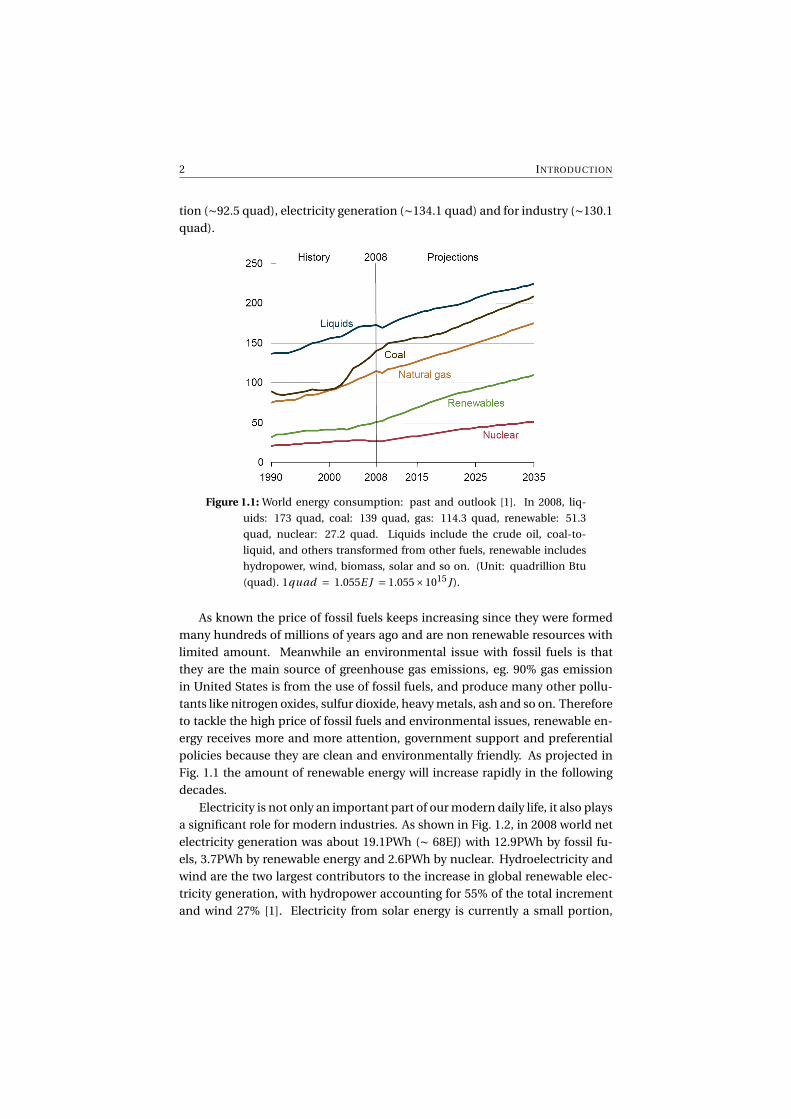
The operation of our modern industrial civilization is wholly dependent ona large amount of energy of various types. Fig. 1.1 shows the world energy con-sumption measured in quadrillion Btu (quad) from the international energyoutlook by the U.S. Energy Information Administration [1]. World energy con-sumption keeps increasing, and in 2008 it amounted to 504.7 quad (∼ 532.5EJ).Fossil fuels (liquids, coal and natural gas) were always and are still the mostpopular energy type. The usage of fossil fuels in 2008 were (estimation basedon data in [1]): 1) Liquids (173 quad): 53.48% goes to transportation, 32.56%to industry, 8.14% to buildings, 5.82% to electricity; 2) Coal (139 quad): 60% toelectricity, 36% to industry, the rest to residential and commercial sectors; 3)Gas (114.3 quad): 35.6% to electricity, 29.3% to industry, the rest to others (eg.residential). Therefore in summary, fossil fuels are mainly used in transporta-
2 INTRODUCTION
tion (∼92.5 quad), electricity generation (∼134.1 quad) and for industry (∼130.1quad).
Figure 1.1: World energy consumption: past and outlook [1]. In 2008, liq-
uids: 173 quad, coal: 139 quad, gas: 114.3 quad, renewable: 51.3
quad, nuclear: 27.2 quad. Liquids include the crude oil, coal-to-
liquid, and others transformed from other fuels, renewable includes
hydropower, wind, biomass, solar and so on. (Unit: quadrillion Btu
(quad). 1quad = 1.055E J = 1.055×10¹⁵ J ).
As known the price of fossil fuels keeps increasing since they were formedmany hundreds of millions of years ago and are non renewable resources withlimited amount. Meanwhile an environmental issue with fossil fuels is thatthey are the main source of greenhouse gas emissions, eg. 90% gas emissionin United States is from the use of fossil fuels, and produce many other pollu-tants like nitrogen oxides, sulfur dioxide, heavy metals, ash and so on. Thereforeto tackle the high price of fossil fuels and environmental issues, renewable en-ergy receives more and more attention, government support and preferentialpolicies because they are clean and environmentally friendly. As projected inFig. 1.1 the amount of renewable energy will increase rapidly in the followingdecades.
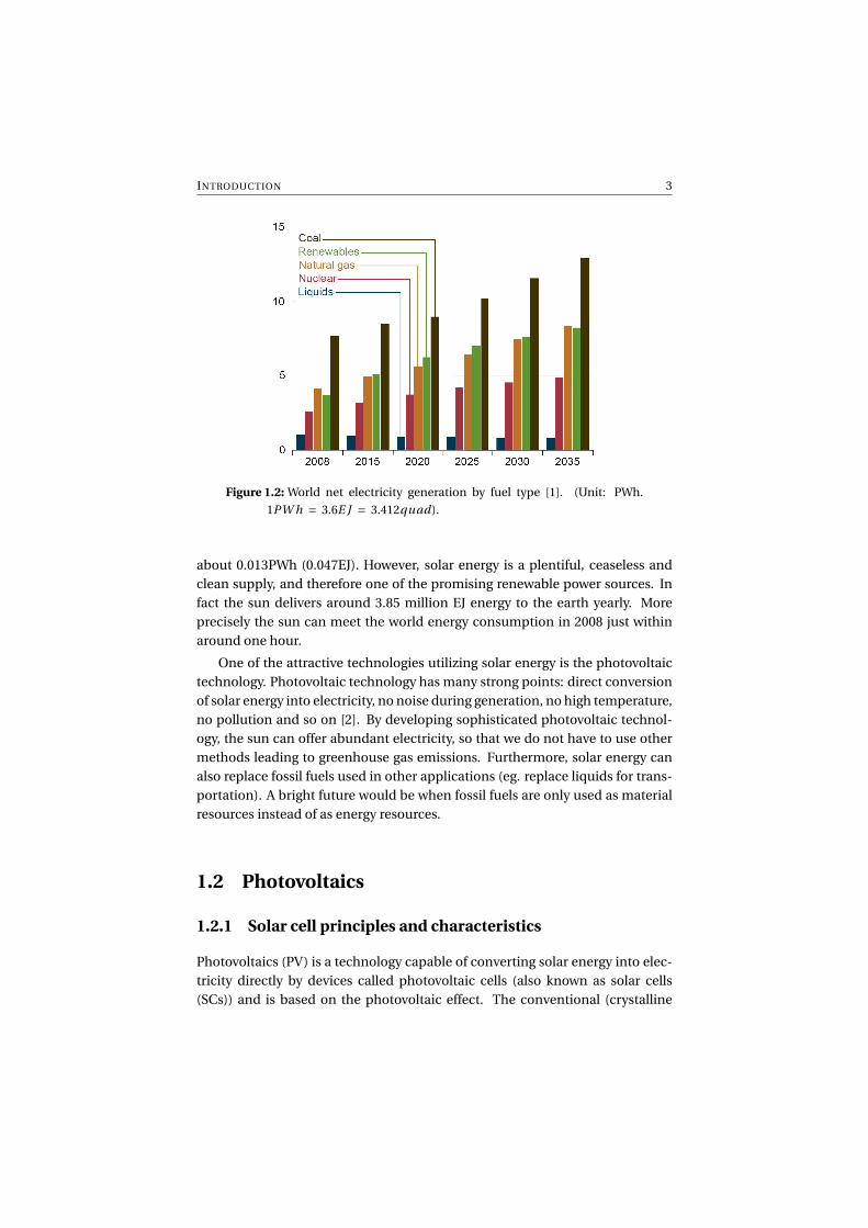
Electricity is not only an important part of our modern daily life, it also playsa significant role for modern industries. As shown in Fig. 1.2, in 2008 world netelectricity generation was about 19.1PWh (∼ 68EJ) with 12.9PWh by fossil fu-els, 3.7PWh by renewable energy and 2.6PWh by nuclear. Hydroelectricity andwind are the two largest contributors to the increase in global renewable elec-tricity generation, with hydropower accounting for 55% of the total incrementand wind 27% [1]. Electricity from solar energy is currently a small portion,
INTRODUCTION 3
Figure 1.2: World net electricity generation by fuel type [1]. (Unit: PWh.
1PW h = 3.6E J = 3.412quad).
about 0.013PWh (0.047EJ). However, solar energy is a plentiful, ceaseless andclean supply, and therefore one of the promising renewable power sources. Infact the sun delivers around 3.85 million EJ energy to the earth yearly. Moreprecisely the sun can meet the world energy consumption in 2008 just withinaround one hour.
One of the attractive technologies utilizing solar energy is the photovoltaictechnology. Photovoltaic technology has many strong points: direct conversionof solar energy into electricity, no noise during generation, no high temperature,no pollution and so on [2]. By developing sophisticated photovoltaic technol-ogy, the sun can offer abundant electricity, so that we do not have to use othermethods leading to greenhouse gas emissions. Furthermore, solar energy canalso replace fossil fuels used in other applications (eg. replace liquids for trans-portation). A bright future would be when fossil fuels are only used as materialresources instead of as energy resources.
1.2 Photovoltaics
1.2.1 Solar cell principles and characteristics
Photovoltaics (PV) is a technology capable of converting solar energy into elec-tricity directly by devices called photovoltaic cells (also known as solar cells(SCs)) and is based on the photovoltaic effect. The conventional (crystalline

4 INTRODUCTION
silicon) solar cells1 typically consist of a p-n junction (formed by p- and n-typesemiconductors into contact) with a single bandgap Eg where voltages are de-veloped by absorbing light.
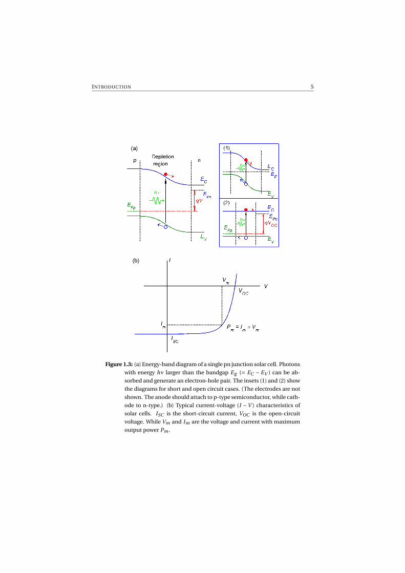
Figure 1.3(a) shows the energy-band diagram for a single p-n junction so-lar cell. When light illuminates the cell, photons with energy hν (ν is the fre-quency and h is the planck constant) larger than the bandgap will be absorbed.Note that not all of the light that satisfies the energy requirement (hν > Eg )is completely absorbed, its absorption characteristic is determined by the in-trinsic absorption coefficient and the thickness of the semiconductor. Mean-while excess energy of the absorbed photon is wasted as heat due to thermaliza-tion in the conduction band. By absorbing a photon an electron in the valenceband is excited into the conduction band, leaving a hole behind and creatingan electron-hole (e-h) pair. These free carriers, e and h, will be swept acrossthe junction by the electric field, collected at the electrodes and can power theexternal load. The electron and hole will transport in the n- and p-type semi-conductor, respectively. During transport to the electrodes recombinations arepossible which will reduce the photocurrent.
Therefore the photovoltaic process in solar cells is generally divided intofour steps: light absorption, charge generation, charge transport and chargecollection. An efficiency can be defined to qualify each step. The product ofthese four efficiencies yields the external quantum efficiency (ηEQE ), whereasthe product of them excluding the absorption efficiency is the internal quan-tum efficiency (ηIQE ). For a good cell the ηEQE should be as large as possible byengineering each step.
For solar cells the most important measure for their performance is howmuch current and voltage they can supply. This can be estimated from the re-lationship between current and voltage, the current-voltage (I-V) characteristic(also known as I-V curve). The I-V curves of solar cells are complex. Ideally theI-V curve with illumination can be derived from solid state physics. It is givenby [3]:
I = I0
(exp
(V
VT
)−1
)− IL (1.1)
where VT is the thermal voltage with a constant value of kT /q , IL is the pho-tocurrent and is identical to the short-circuit current (ISC ), I0 is the ideal reversesaturation current. The first term on the right represents the current without il-lumination.
Figure 1.3 (b) shows the typical I-V curve. From this figure we can extractseveral important parameters to characterize solar cell performance: the open-circuit voltage VOC , the short-circuit current ISC , the maximum power output
1The operational principle of organic solar cells is similar, however differences are explained insection 1.3.1.
INTRODUCTION 5
Figure 1.3: (a) Energy-band diagram of a single pn junction solar cell. Photons
with energy hν larger than the bandgap Eg (= EC −EV ) can be ab-
sorbed and generate an electron-hole pair. The insets (1) and (2) show
the diagrams for short and open circuit cases. (The electrodes are not
shown. The anode should attach to p-type semiconductor, while cath-
ode to n-type.) (b) Typical current-voltage (I −V ) characteristics of
solar cells. ISC is the short-circuit current, VOC is the open-circuit
voltage. While Vm and Im are the voltage and current with maximum
output power Pm .

6 INTRODUCTION
Pm , and the filling factor F F . The maximum power output Pm is achievablewith an appropriate external load. The open-circuit voltage VOC is the availablemaximum voltage of solar cells and qualitatively the built-in potential of thep-n junction. It is somewhat smaller than the bandgap, as seen in Fig. 1.3 (a).Therefore using semiconductor materials with large bandgap can increase theVOC , however the photocurrent will decrease since a larger Eg limits the lightabsorption. The short-circuit current ISC is the current when the external circuitis shorted by an ideal conductor. It can be directly calculated by integrating thephotogenerated charges under solar irradiance, and is given by
ISC = A · JSC = Ae
hc
∫ληA(λ)S(λ)dλ (1.2)
where A is the area of the electrode in contact with the semiconductor, S(λ) isthe solar irradiance spectrum, ηA(λ) is the absorption spectrum of the activelayer in the solar cell, and e is the elementary charge (1.6×10⁻¹⁹ C). Instead ofISC , the short circuit current density JSC is commonly used since it is indepen-dent of the area A. The filling factor F F is the ratio of Pm to the product of ISC
and VOC :
F F = Vm · Im
VOC · ISC. (1.3)
For a good conventional solar cell a filling factor as high as 80% can be achieved.The power conversion efficiency is the most important figure of merit, de-
fined as the ratio of photo-generated electric output power to the total incidentpower on the solar cell. It is given by
η= Pm
Pi n= Vm · Im
Pi n= F F ·VOC · ISC
Pi n. (1.4)
The total power (also called intensity) of incident light Pi n is given by the inte-gration of the solar spectrum over all wavelengths:
Pi n =∫
S(λ)dλ. (1.5)
Eq. 1.4 reveals that the efficiency of a solar cell is influenced by both ISC andVOC , and both are influenced by the semiconductor bandgap. The ideal max-imum efficiency achievable for a single junction solar cell with optimizedbandgap is ∼31% under the AM 1.5G illumination condition with 1 sun at300K [3].
From Eqs. 1.2 and 1.4 one can see that both the short circuit current andpower conversion efficiency are dependent on the light intensity and its ir-radiance spectrum. Therefore different light sources will result in differentcharacteristics of the solar cell. To have a comparison between different solarcells, a standard light source is need defined. The global air mass 1.5 (AM 1.5G)

INTRODUCTION 7
spectrum is the commonly used solar irradiance for solar cell characterization(shown in Fig. 1.4). It has a total intensity of 100mW/cm2 when integratedacross the whole solar spectrum.
Figure 1.4: AM 1.5G solar irradiance spectrum.
1.2.2 Solar cell generations
The photovoltaic effect was first discovered by Becquerel in 1839 [4] in a junc-tion formed between an electrode and an electrolyte. Since then many effortshave been dedicated to investigate other materials and improve the efficienciesof solar cells. However the efficiencies remained low, until 1954 when there weretwo breakthroughs. Chapin et al. at Bell Laboratories developed the first siliconsolar cells with a large efficiency [5], whereas Reynolds et al. at Aeronautical Re-search Laboratory demonstrated cadmium sulfide cells with short circuit cur-rents of 15mA/cm2 and open circuit voltages of 0.4V under direct sunlight [6].Over the last 50 years solar cells have received tremendous improvements. Todate, solar cells have reached a record efficiency of 28.3% for a single junctioncells [7] and 43.5% for multi-junction cells [8]. Since the first Si cell in 1954 solarcells have experienced three generations regarding the materials and technolo-gies used [9].
The first generation solar cells, also called conventional solar cells, are madefrom silicon, like crystalline silicon (c-Si), multicrystalline silicon (mc-Si) andribbons. They are currently very efficient and the most dominant solar cellsavailable in the market. In 2009 this kind of solar cells was responsible foraround 75% of the worldwide solar cell production. However as known Si isa weakly absorbing material (due to its indirect band gap) so the crystallinesilicon wafer based solar cells are always very thick, about 180-300µm. Mean-while Si crystals are expensive and slow to grow due to the production process.
8 INTRODUCTION
Therefore the cost of first generation solar cells remains high. Moreover, theyare fragile and heavy.
The second generation of solar cells usually refers to thin-film solar cells,which are mainly made from three different semiconductor materials includ-ing amorphous silicon (a-Si), cadmium telluride (CdTe) and copper indium gal-lium selenide (CIS or CIGS). Compared with c-Si based solar cells, thin-film so-lar cells are at least 100 times thinner, which make them very light so they aredeposited on a (possibly flexible) substrate for mechanical support. They canbe produced on a much larger scale with no requirement for high temperatureprocesses (∼ 200◦). As a consequence they have attractive properties over c-Siand are eventually much cheaper, which to some extent can balance the lowerefficiency of thin-film solar cells.
Most of the third generation solar cells are in the research phase, and alsobelong to the thin-film class with respect to their ultrathin active layer thick-ness. Two representative technologies are the dye-sensitized solar cells (DSSCs)and organic solar cells (OSCs). DSSCs currently seem to be the most efficientthird generation cells with a demonstrated efficiency around 13% [10]. OSCshave a slightly lower efficiency, so far the record cell has an efficiency of 10.6%with a tandem structure by Yang Yang Laboratory at the University of California,Los Angeles [11]. Meanwhile some companies like Mitsubishi Chemical and He-liatek also reported cells with efficiency around 10% in 2011 [12, 13]. Comparedwith conventional cells OSCs are a potentially cheap and simple alternative en-ergy source with good mechanical flexibility, feather-weight, and easy produc-tion. However the stability of OSCs remains a problem, and their efficienciesdepend on the morphology of the active layer.
1.3 Organic solar cells
A typical OSC usually consists of four layers: an ITO coated substrate (glass orflexible materials), followed by a layer of poly(3,4-ethylenedioxythiophene):poly(styrenesulfonate) (PEDOT:PSS), then the active layer and reflector (usually asanode). The PEDOT:PSS layer serves as a hole transport and exciton block-ing layer. Similar to conventional cells the active layer of OSCs is made fromtwo different organic semiconductor materials, one is an electron donor (D)and the other is an electron acceptor (A). The donors can be divided intotwo different categories, small molecule and polymers. Some commonly usedsmall molecules are Copper phthalocyanine (CuPc), chloro [subphthalocyan-inato] boron (SubPc), Zinc phthalocyanine (ZnPc) and so on. While somewell developed polymers are poly(3-exylthiophene) (P3HT), poly[(4,40-bis(2-ethylhexyl)dithieno[3,2-b:20,30-d] silole )-2,6-diyl-alt-(2,1,3- benzothiadia-zole )-4,7-diyl] (PSBTBT), poly[2,6-(4,4- bis-(2-ethylhexyl)-4H-cyclopenta[2,1-

INTRODUCTION 9
b;3,4-b’] dithiophene)-alt-4,7-(2,1,3- benzothiadiazole )] (PCPDTBT) and soon [14–16]. Good electron acceptors are buckminster fullerene C60 and itsderivatives like indene-C60 bisadduct (ICBA), [6,6]-phenyl-C71-butyric acidmethyl ester (PC70BM), [6,6]-phenyl-C61 butyric acid methyl ester (PCBM) andso on [14–16]. The small molecule solar cells are usually fabricated with ther-mal evaporation processes. In contrast polymer solar cells are usually made viasolution based technologies, such as spin coating, doctor blading and print-ing [17].
1.3.1 General working principles
Figure 1.5 shows the operation mechanism of an OSC [18]. There are severalsteps involved for photocurrent generation [16–18]: 1) Generation of excitonsin donor and/or acceptor from light absorption by exciting an electron from thehighest occupied molecular orbital (HOMO) to the lowest unoccupied molec-ular orbital (LUMO). Different from the weakly Coulomb bound electron-holepairs generated in inorganic solar cells, the exciton is a strongly bound electron-hole pair; 2) Excitons have to diffuse to a D-A interface; 3) Exciton dissociationat the D-A interface, transferring to charge carriers, i.e. free electron and hole; 4)Charge transport to and collection by the electrodes. For each step an efficiencyfactor can be defined [16–18]:
1. Absorption efficiency ηA , defined as the ratio of the number of photo-generated excitons to that of incident photons.
2. Exciton diffusion efficiency ηED , defined as the ratio of the number of dif-fusing excitons to a D-A interface to that of photo-generated excitons.
3. Charge transfer efficiency ηC T , defined as the ratio of the number of dis-sociated excitons at a D-A interface to that of diffusing excitons to a D-Ainterface.
4. Charge collection efficiency ηCC , defined as the ratio of the number offree charge carriers collected at electrodes to that of dissociated excitonsat a D-A interface.
Then the internal (ηIQE ) and external (ηEQE ) quantum efficiencies are givenby:
ηIQE = ηED ·ηC T ·ηCC (1.6)
ηEQE = ηA ·ηIQE = ηA ·ηED ·ηC T ·ηCC (1.7)
OSCs with ηIQE close to 100% have been demonstrated with an active layer(PCPDTBT:PC70BM) thickness of 80nm [19]. Therefore the absorption is mainly
10 INTRODUCTION
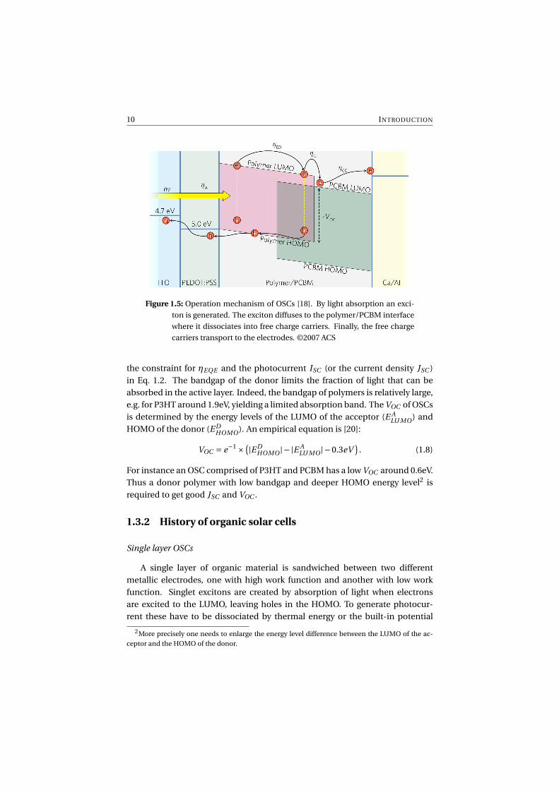
Figure 1.5: Operation mechanism of OSCs [18]. By light absorption an exci-
ton is generated. The exciton diffuses to the polymer/PCBM interface
where it dissociates into free charge carriers. Finally, the free charge
carriers transport to the electrodes. ©2007 ACS
the constraint for ηEQE and the photocurrent ISC (or the current density JSC )in Eq. 1.2. The bandgap of the donor limits the fraction of light that can beabsorbed in the active layer. Indeed, the bandgap of polymers is relatively large,e.g. for P3HT around 1.9eV, yielding a limited absorption band. The VOC of OSCsis determined by the energy levels of the LUMO of the acceptor (E A
LU MO) andHOMO of the donor (E D
HOMO). An empirical equation is [20]:
VOC = e−1 × (|E DHOMO |− |E A
LU MO |−0.3eV)
. (1.8)
For instance an OSC comprised of P3HT and PCBM has a low VOC around 0.6eV.Thus a donor polymer with low bandgap and deeper HOMO energy level2 isrequired to get good JSC and VOC .
1.3.2 History of organic solar cells
Single layer OSCs
A single layer of organic material is sandwiched between two differentmetallic electrodes, one with high work function and another with low workfunction. Singlet excitons are created by absorption of light when electronsare excited to the LUMO, leaving holes in the HOMO. To generate photocur-rent these have to be dissociated by thermal energy or the built-in potential
2More precisely one needs to enlarge the energy level difference between the LUMO of the ac-ceptor and the HOMO of the donor.

INTRODUCTION 11
overcoming the binding energy. The built-in potential can be either from thedifference of work function between the electrodes or from a Schottky contactat the metal/organic contacts [21, 22]. However the built-in potential setup bythe difference of work function of electrodes, for instance indium tin oxide, ITO,and Al, is not high enough to obtain efficient dissociation. In most cases it usesthe Schottky contact cell structure formed between a p-type organic materialand a metal with low work function [14, 23]. The exciton will be dissociated atthe depletion region of the Schottky contact.
Upon light absorption excitons are generated in the whole organic material.However dissociation can only happen at the depletion region near the metalcontact. Due to the short diffusion length of excitons (typically on the order of10nm) [24–26], most of them get recombined before their dissociation duringdiffusion to the depletion region. Meanwhile, after dissociation both electronsand holes have to travel in the same material before reaching the electrodes,leaving a large possibility for bimolecular recombination [17]. Therefore thistype of OSCs has limited power conversion efficiencies, much less than 1% [27–29].
Bilayer OSCs
The next breakthrough was achieved by applying donor-accepter (D-A)concepts. In 1984 Tang reported a novel bilayer OSC with about 0.95% powerconversion efficiency under simulated AM2 illumination conditions, fabricatedfrom CuPc (donor, as the p-type semiconductor) and a perylene tetracarboxylicderivative (acceptor, as n-type semiconductor) [30]. The improved efficiencycompared with single layer structures is mainly due to a more efficient chargedissociation. These two layers of materials have differences in electron affinityand ionization energy. The energy level offset at the interface between the twolayers can be very large (by choosing proper materials) and yield strong localelectric fields. Excitons generated by light absorption dissociate more efficientlyat the interface, compared with dissociation by the built-in potential in a singlelayer structure. After dissociation charge carriers are transported in differentorganic materials, holes in the donor and electrons in the acceptor. This canreduce bimolecular recombination to a great extent.
Later on by using new materials like buckminster fullerene, C60 conjugatedpolymer poly(phenylene vinylene) (PPV) and their derivatives, the conversionefficiencies of bilayer structure solar cells have improved up to 1–4%. Howeverthe bilayer structure still suffers from the limited exciton diffusion range in or-ganic materials.
Bulk heterojunction OSCs
Although the bilayer structure is a big improvement, still a considerable

12 INTRODUCTION
amount of excitons recombine during diffusion to the D-A interface. Usuallythicknesses of OSCs are on the order of 100nm, whereas the diffusion length istypically on the order of 10nm. Therefore, an advanced OSC structure calledbulk heterojunction (BHJ) was invented. The BHJ is formed by intimately mix-ing the donor and the accepter. This concept was first developed for the smallmolecule solar cells in 1992 by Hiramoto et al. by co-evaporating donor andacceptor molecules under high-vacuum conditions [31]. Later this concept wasextended to polymer solar cells in 1995 by Heeger’s group [32]. Relatively highefficiencies around 4–5% have been demonstrated using a polymer mixture ofP3HT and PCBM [33–35]. For polymer solar cells several solution processingtechniques can be used to fabricate BHJ OSCs, such as spin coating, screenprinting, spray coating and so on. As shown in Fig. 1.6 the D-A interface in aBHJ is spatially distributed throughout the whole active layer, instead of a pla-nar D-A heterojunction in the bilayer structure. The benefit is that excitons canbe efficiently and ideally dissociated within their lifetime. Similar with bilayerstructures the charge carriers are separated and transported within organicmaterials, which results in a good conversion efficiency. The morphology ofthe active layer is critical for the performance of BHJ OSCs, since only excitonscreated within the diffusion length contribute. Therefore several morphologycontrol methods have been developed, such as thermal annealing [34, 36, 37]and the addition of processing additives [38, 39].
Figure 1.6: Schematic diagram of bulk heterojunction structure of OSCs to-
gether with the processes involved. Signs ‘⊕’ and ‘ª’ denote hole and
electron.

INTRODUCTION 13
1.4 Light trapping
A key challenge for crystalline silicon cells remains that the absorption is alwaysrelatively weak in the near infrared, due to the indirect band gap. In order to getconsiderable efficiency solar cells have to absorb sunlight as much as possible.This consequently requires a thick active layer, a few hundred microns, beforelight gets absorbed. Together with the concomitant increasing carrier diffusionlength requirement, material cost is driven higher. Therefore it is always a trade-off between efficiency and material cost for traditional solar cells. On the otherhand, organic materials have a lower carrier mobility and require exciton disso-ciation, which limits the active layer thickness. However thin active layers havepoor light absorption. Therefore light trapping is needed in order to bring downthe thickness, yet to still provide a quite efficient absorption.
For traditional solar cells, light trapping is usually achieved by introducingmicrometer scale pyramid-like surface textures to increase surface roughness.From ray optics theory, the light path compared to a single pass can be en-hanced up to a limiting factor of 4n2 [40], where n is the refractive index of theactive material. This limit is applicable in the framework of ray optics, wherewave effects like diffraction and interference are negligible. To achieve this limita Lambertian roughness has to be introduced which has an isotropic response.Meanwhile it is mainly valid for an active layer of about a few hundred microns,and for wavelengths near the band edge where the intrinsic absorption coeffi-cient is low. The enhancement factor drops tremendously at wavelengths wherea large absorption coefficient is present.
This 4n2 limit becomes invalid for thin-film solar cells such as OSCs whichhave thin active layers comparable with the wavelength, usually only 100–200nm thick, and have a high absorption coefficient. Since for thin-film solarcells the wave character of light becomes significant, trapping approaches haveto be considered in the framework of wave optics. Recently, theoretical studiesbased on statistical coupled mode theory have shown the possibility to surpassthe 4n2 limit in a thin-film Si solar cell (with a few micron thickness) by a gratingstructure in the wave optics regime [41]. In [41] they have derived that a max-imum absorption enhancement limit of 4πn2 can be achieved by 2D gratingswith a square lattice, for 0 < s < 1, where s is the ratio of grating period to thewavelength. For a triangular lattice this enhancement limit can be as high as8πn2/
p3 for 0 < s < 2/
p3. The maximum enhancement converges to the limit
of 4n2 for large values of s (corresponding to the Lambertian limit).
In general any photonic structure or phenomenon that exhibits energy con-finement is potentially useful for light trapping. Many trapping schemes areproposed and investigated theoretically and experimentally for thin-film solarcells (both inorganic and organic), such as 2D or 3D photonic crystals [42–45],

14 INTRODUCTION
dielectric gratings [46–52], folded structures [53, 54], metallic nanoparticles [55–68], metallic gratings [69–85] and so on. All of these schemes try to increase thephoton density in solar cells, specifically in the active layer, by exploiting somephotonic phenomena like diffraction, interference, cavity resonances, guidedmodes, surface plasmons and so on.
Recently, metallic nanostructures, such as metallic nanoparticles and grat-ings, have received considerable attention for their ability to concentrate andmanipulate light at the nanoscale, and thus for light trapping. Plasmonic modescan, in general, be classified into two categories: localized surface plasmons(LSPs) and propagating surface plasmon polaritons (SPPs). The former are as-sociated with very local excitations, such as around nanoparticles. The latterare associated with surfaces, along which a mode can propagate. Both LSPs andSPPs create mainly two effects: enhanced near-field intensities and enhancedscattering of light. A recent review by Atwater et al. [86] concerning the inter-section of plasmonics and photovoltaics has summarized the commonly usedplasmonic light trapping schemes (see Fig. 1.7). In general there are three differ-ent schemes, one with metallic nanostructures on top of the cells as scatteringelements (Fig. 1.7(a)), one with structures inside as antennas (Fig. 1.7(b)), andthe last one with structures integrated with the metallic back contact where lightcan be coupled into SPP modes and other guided modes in the layered device(Fig. 1.7(c)). More details about plasmonic phenomena are provided in chapter2.
Figure 1.7: Plasmonic light trapping schemes for thin-film solar cells [86]. (a)
Light trapping by scattering from metal nanostructures at the surface
of the solar cell. (b) Light trapping by excitation of localized surface
plasmons in particles embedded in the active layer. (c) Light trap-
ping by the excitation of surface plasmon polaritons at the metal/ac-
tive layer interface. ©2010 Macmillan Publishers Limited.
1.5 Objectives and thesis outline
Organic solar cells enjoy a strong potential compared to inorganic solar cells, forexample because of the possibility of low-cost fabrication of lightweight, large-
INTRODUCTION 15
area devices. However, important issues such as low efficiencies and stabilityneed to be addressed. So far the efficiency of OSCs is still around the 10% effi-ciency barrier. In early 2012 Yang’s group set a new world record with an effi-ciency of 10.6% with a tandem device [11].
The low efficiency limitation is mainly imposed by the short exciton diffu-sion length in organic materials, which is typically around 10nm, and also otheraspects such as the relative bandgap and low energy level of the donor HOMO.This diffusion length is much smaller than the light absorption length in or-ganic materials, usually 100–200nm. Therefore there is an important tradeoffbetween optical and electronic properties, leading to the challenge to absorbas much light as possible in an active layer as thin as possible. To achieve this,nanophotonic light trapping schemes offer help.
The work presented in this thesis is part of the IWT-SBO Polyspec project,which aimed at increasing the energy conversion efficiency of organic bulkheterojunction photovoltaic devices, as well as improving the stability of theirnanomorphology, involving material development, morphological analysis andmodeling, optical modeling and so on. Our work focused on optical modelingof the use of metallic nanostructures for light harvesting, as these elements tendto be very compact, and seem at first sight compatible with OSCs.
At the onset of this work, only preliminary results on plasmonic enhance-ment of organic devices, such as solar cells and organic LEDs, were available.Therefore the potential of metallic nanostructures in OSCs remained an openquestion. Here we summarize our findings using theoretical and numerical ap-proaches, on the use of various metallic nanostructures, such as particles andgratings, to enhance the light absorption in OSCs.
The text is organized as follows. In chapter 2 various basic concepts are ex-plained. There we introduce the surface plasmon mode at interfaces, the ana-lytical Mie theory for plasmonic modes in spheroid metallic nanoparticles, andthe numerical modeling tools we use throughout this work. In chapter 3 we fo-cus on utilizing metallic nanoparticles for light absorption enhancement. Westart with a simplified 2D model to analyze the absorption enhancement mech-anism. Then we extend to a more concrete 3D model. In chapter 4 we exam-ine metallic gratings by exploiting both SPPs and LSPs for an efficiency boost.We combine front and back gratings together, to have an additive enhancementfrom each grating. In chapter 5 gratings with tapered slits are examined. By ta-pering we see an enhanced and broadened transmission, which may be usefulfor light harvesting in solar cells. Finally chapter 6 provides conclusions andperspectives for the future work.
16 INTRODUCTION
1.6 Publications
Publications in international journals
1. B. Niesen, B.P. Rand, P. Van Dorpe, D. Cheyns, H. Shen, B. Maes, and P.Heremans. Near-field interactions between metal nanoparticle surfaceplasmons and molecular excitons in thin-films. Part I: absorption. 2012.(Submitted)
2. H. Shen, and B. Maes. Enhanced optical transmission through taperedmetallic gratings. Applied Physics Letters, 100(24):241104, June 2012.
3. R. Morarescu, H. Shen, R. A. L. Vallée, B. Maes, B. Kolaric, and P. Damman.Exploiting the Localized Surface Plasmon Modes in Gold Triangular Nanopar-ticles for Sensing Applications. Journal of Materials Chemistry, 22(23):11537-11542, May 2012
4. H. Shen, and B. Maes. Combined plasmonic gratings in organic solar cells.Optics Express, 19(S6):A1202-A1210, November 2011.
5. A. Abass, H. Shen, P. Bienstman, and B. Maes. Angle insensitive enhance-ment of organic solar cells using metallic gratings. Journal of AppliedPhysics, 109(2):023111, January 2011.
6. B. Niesen, B. P. Rand, P. Van Dorpe, H. Shen, B. Maes, J. Genoe, and P. Here-mans. Excitation of multiple dipole surface plasmon resonances in spheri-cal silver nanoparticles. Optics Express, 18(18):19032-19038, August 2010.
7. H. Shen, P. Bienstman, and B. Maes. Plasmonic absorption enhancementin organic solar cells with thin active layers. Journal of Applied Physics,106(7):073109, October 2009.
Publications in international conferences
8. H. Shen, A. Abass, M. Burgelman, B. Maes, Tailored and tapered metal-lic gratings for enhanced absorption or transmission. In ICTON (Inter-national Conference on Transparent Optical Networks) (invited), UnitedKingdom, 2012. (to be published)
9. H. Shen, A. Abass, M. Burgelman, B. Maes, Thin-film solar cells with com-bined metallic enhancements. MINAP (Micro- and nano-photonic mate-rials and devices), page 103-104, Italy, 2012.
10. H. Shen, and B. Maes. Plasmonic enhancement in organic solar cellswith metallic gratings. In 16th Annual Symposium of the IEEE PhotonicsBenelux Chapter, page 21–24, Ghent, Belgium, December 2011.

INTRODUCTION 17
11. H. Shen, and B. Maes. Combined Plasmonic Gratings in Thin Organic So-lar Cells. In Photonics Prague 2011, page 73, Czech Republic, 2011.
12. A. Abass, H. Shen, K. Quang Le, P. Bienstman, and B. Maes. On the an-gular dependent nature of absorption enhancement in organic solar cellsby metallic nanostructures. In 8th International Symposium on ModernOptics and Its Applications, page PP-07, Indonesia, 2011.
13. B. Maes, A. Abass, H. Shen, and P. Bienstman. Plasmonic absorptionenhancement in organic photovoltaics. In ICTON (International Confer-ence on Transparent Optical Networks) (invited), page We.A2.5, Germany,2010.
14. A. Abass, H. Shen, P. Bienstman, and B. Maes. Increasing Polymer SolarCell Efficiency with Triangular Silver Gratings. In Optical Nanostructuresfor Photovoltaics (PV) (invited), page PWA5, Germany, 2010.
15. B. Maes, H. Shen, and P. Bienstman. Plasmonic nanoparticle enhance-ment in thin organic solar cells. In ICTON (International Conference onTransparent Optical Networks) Mediterranean Winter - COST MP0702workshop, page Fr3B.5 ,France, 2009.
16. H. Shen, P. Bienstman, and B. Maes. Absorption enhancement in organicsolar cells by metallic nanoparticles. In 14th Annual Symposium of theIEEE Photonics Benelux Chapter, page 85–88, Brussels, Belgium, Novem-ber 2009.
Publications in national conferences
17. H. Shen, and B. Maes. Metallic grating enhanced absorption in organicsolar cells. In 12th FEA PhD Symposium, page 98, Ghent, Belgium, De-cember 2011.
18. H. Shen, P. Bienstman, and B. Maes. Absorption enhancement in organicsolar cells by metallic nanoparticles. In 10th UGent-FirW PhD Sympo-sium, pages 290-291, Ghent, Belgium, December 2009.
18 INTRODUCTION
References
[1] U.S. Energy Information Administration. International Energy Outlook2011, September 2011.
[2] A. Goetzberger and V. U. Hoffmann. Photovoltaic Solar Energy Generation,volume 112. Springer Verlag, 2005.
[3] S. M. Sze and K. K. Ng. Semiconductor Devices: Physics and Technology.John Wiley & Sons, third edition edition, 2007.
[4] A. E. Becquerel. On electric effects under the influence of solar radiation.Compt. Rend. Acad. Sci., 9:561, 1839.
[5] D. M. Chapin, C. S. Fuller, and G. L. Pearson. A New Siliconp-n JunctionPhotocell for Converting Solar Radiation into Electrical Power. Journal ofApplied Physics, 25:676, 1954.
[6] D. C. Reynolds, G. Leies, and R. E. Antes, L. L. and. Marburger. PhotovoltaicEffect in Cadmium Sulfide. Physical Review, 96(2):533–534, 1954.
[7] M. A. Green, K. Emery, Y. Hishikawa, W. Warta, and E. D. Dunlop. Solarcell efficiency tables (version 39). Progress in Photovoltaics: Research andApplications, 20(1):12–20, 2012.
[8] H. Yuen. High Efficiency Solar Cells at Solar Junction. In Optics for SolarEnergy. Optical Society of America, 2011.
[9] A. Goetzberger, J. Luther, and G. Willeke. Solar cells : past , present , future.Solar Energy, 74:1–11, 2002.
[10] A. Yella, H. W. Lee, H. N. Tsao, C. Yi, A. K. Chandiran, M. K. Nazeeruddin,E. W. G. Diau, C. Y. Yeh, S. M. Zakeeruddin, and M. Grätzel. Porphyrin-Sensitized Solar Cells with Cobalt (II/III)–Based Redox Electrolyte Exceed 12Percent Efficiency. Science, 334(6056):629–634, 2011.
[11] W. W. Kromhout. UCLA engineers create tandem polymer solar cells that setrecord for energy-conversion. Technical report, University of California, LosAngeles, February 2012.
[12] http://www.independent.co.uk/environment/sprayon-solar-may-be-future-for-green-energy 2343590.html.
[13] http://www.heliatek.com/.
[14] H. Hoppe and N. S. Sariciftci. Organic solar cells: An overview. Journal ofMaterials Research, 19(7):1924–1945, 2004.
INTRODUCTION 19
[15] J. Y. Kim, K. Lee, N. E. Coates, D. Moses, T. Q. Nguyen, M. Dante, and A. J.Heeger. Efficient tandem polymer solar cells fabricated by all-solution pro-cessing. Science, 317(5835):222–225, 2007.
[16] G. Li, R. Zhu, and Y. Yang. Polymer solar cells. Nature Photonics, 6(3):153–161, 2012.
[17] T. Soga, editor. Nanostructured Materials for Solar Energy Conversion. El-sevier, Amsterdam, The Netherlands, first edition edition, 2006.
[18] X. Yang and J. Loos. Toward high-performance polymer solar cells: The im-portance of morphology control. Macromolecules, 40(5):1353–1362, 2007.
[19] S. H. Park, A. Roy, S. Beaupré, S. Cho, N. Coates, J. S. Moon, D. Moses,M. Leclerc, K. Lee, and A. J. Heeger. Bulk heterojunction solar cells with in-ternal quantum efficiency approaching 100%. Nature Photonics, 3(5):297–302, 2009.
[20] M. C. Scharber, D. Mühlbacher, M. Koppe, P. Denk, C. Waldauf, A. J.Heeger, and C. J. Brabec. Design rules for donors in bulk-heterojunction so-lar cellsałTowards 10% energy-conversion efficiency. Advanced Materials,18(6):789–794, 2006.
[21] D. Wohrle and D. Meissner. Organic Solar Cells. Advanced Materials, 3:129–138, 1991.
[22] C. J. Brabec and N. S. Sariciftci. Plastic solar cells. Advanced FunctionalMaterials, (1):15–26, 2001.
[23] G. Chamberlain. Organic solar cells: A review. Solar Cells, 8(1):47–83, 1983.
[24] J. J. M. Halls, K. Pichler, R. H. Friend, S. C. Moratti, and A. B. Holmes. Exci-ton diffusion and dissociation in a poly (p-phenylenevinylene)/C60 hetero-junction photovoltaic cell. Applied physics letters, 68:3120, 1996.
[25] L. A. A. Pettersson, L.S. Roman, and O. Inganäs. Modeling photocurrentaction spectra of photovoltaic devices based on organic thin films. Journalof Applied Physics, 86:487, 1999.
[26] P. E. Shaw, A. Ruseckas, and I. D. W. Samuel. Exciton diffusion measure-ments in poly (3-hexylthiophene). Advanced Materials, 20(18):3516–3520,2008.
[27] A. K. Ghosh and T. Feng. Merocynanine organic solar cells. Journal of Ap-plied Physics, 49(12):5982–5989, 1978.
20 INTRODUCTION
[28] D. L. Morel, A. K. Ghosh, T. Feng, E. L. Stogryn, P. E. Purwin, R. F. Shaw, andC. Fishman. High-efficiency organic solar cells. Applied Physics Letters,32(8):495–497, 1978.
[29] C Brabec. Organic photovoltaics: technology and market. Solar EnergyMaterials and Solar Cells, 83(2-3):273–292, 2004.
[30] C. W. Tang. Two-layer organic photovoltaic cell. Applied Physics Letters,48(2):183, 1986.
[31] M. Hiramoto, H. Fujiwara, and M. Yokoyama. p-i-n like behavior in three-layered organic solar cells having a co-deposited interlayer of pigments.Journal of Applied Physics, 72(8):3781–3787, 1992.
[32] G. Yu, J. Gao, J. C. Hummelen, F. Wudl, and A. J. Heeger. Polymer photo-voltaic cells: enhanced efficiencies via a network of internal donor-acceptorheterojunctions. Science, 270(5243):1789–1791, 1995.
[33] G. Li, V. Shrotriya, J. Huang, Y. Yao, T. Moriarty, K. Emery, and Y. Yang.High-efficiency solution processable polymer photovoltaic cells by self-organization of polymer blends. Nature Materials, 4(11):864–868, 2005.
[34] W. Ma, C. Yang, X. Gong, K. Lee, and A. J. Heeger. Thermally stable, efficientpolymer solar cells with nanoscale control of the interpenetrating networkmorphology. Advanced Functional Materials, 15(10):1617–1622, 2005.
[35] Y. Kim, S. Cook, S. M. Tuladhar, S. A. Choulis, J. Nelson, J. R. Durrant,D. D. C. Bradley, M. Giles, I. McCulloch, C.-S. Ha, and M. Ree. A strongregioregularity effect in self-organizing conjugated polymer films and high-efficiency polythiophene:fullerene solar cells. Nature Materials, 5(3):197–203, 2006.
[36] F. Padinger, R. S. Rittberger, and N. S. Sariciftci. Effects of postproductiontreatment on plastic solar cells. Advanced Functional Materials, 13(1):85–88, 2003.
[37] H. Hoppe and N. S. Sariciftci. Morphology of polymer/fullerene bulk hetero-junction solar cells. Journal of Materials Chemistry, 16(1):45–61, 2006.
[38] J. Peet, J. Y. Kim, N. E. Coates, W. L. Ma, D. Moses, A. J. Heeger, and G. C.Bazan. Efficiency enhancement in low-bandgap polymer solar cells by pro-cessing with alkane dithiols. Nature Materials, 6(7):497–500, 2007.
[39] J. K. Lee, W. L. Ma, C. J. Brabec, J. Yuen, J. S. Moon, J. Y. Kim, K. Lee, G. C.Bazan, and A. J. Heeger. Processing additives for improved efficiency frombulk heterojunction solar cells. Journal of the American Chemical Society,130(11):3619–3623, 2008.

INTRODUCTION 21
[40] E. Yablonovitch. Statistical ray optics. Journal of Optical Society of America,72(7):899–907, 1982.
[41] Z. Yu, A. Raman, and S. Fan. Fundamental limit of light trapping in gratingstructures. Optics Express, 18(103):A366–A380, 2010.
[42] L. Zeng, Y. Yi, C. Hong, J. Liu, N. Feng, X. Duan, L. C. Kimerling, and B. A.Alamariu. Efficiency enhancement in Si solar cells by textured photonic crys-tal back reflector. Applied Physics Letters, 89(11):111111, 2006.
[43] P. Bermel, C. Luo, L. Zeng, L. C. Kimerling, and J. D. Joannopoulos. Improv-ing thin-film crystalline silicon solar cell efficiencies with photonic crystals.Optics Express, 15(25):16986–17000, 2007.
[44] Y. Park, E. Drouard, O. E. Daif, X. Letartre, A. Fave, A. Kaminski, M. Lemiti,and C. Seassal. Absorption enhancement using photonic crystals for siliconthin film solar cells. Optics Express, 17(16):14312–14321, 2009.
[45] J. R. Tumbleston, D.-H. Ko, E. T. Samulski, and R. Lopez. Absorption andquasiguided mode analysis of organic solar cells with photonic crystal pho-toactive layers. Optics Express, 17(9):7670–81, 2009.
[46] S. H. Zaidi, J. M. Gee, and D. S. Ruby. Diffraction grating structures in so-lar cells. In Photovoltaic Specialists Conference. Conference Record of theTwenty-Eighth IEEE, pages 395–398. IEEE, 2000.
[47] C. Eisele, C. E. Nebel, and M. Stutzmann. Periodic light coupler gratings inamorphous thin film solar cells. Journal of Applied Physics, 89:7722, 2001.
[48] S. H. Zaidi, R. Marquadt, B. Minhas, and J. W. Tringe. Deeply etched grat-ing structures for enhanced absorption in thin c-Si solar cells. In Pho-tovoltaic Specialists Conference. Conference Record of the Twenty-NinthIEEE, pages 1290–1293. IEEE, 2002.
[49] M. Niggemann, M. Glatthaar, A. Gombert, A. Hinsch, and V. Wittwer.Diffraction gratings and buried nano-electrodesałarchitectures for organicsolar cells. Thin Solid Films, 451:619–623, 2004.
[50] F. Llopis and I. Tobias. The role of rear surface in thin silicon solar cells.Solar Energy Materials and Solar Cells, 87(1):481–492, 2005.
[51] S. I. Na, S. S. Kim, J. Jo, S. H. Oh, J. Kim, and D. Y. Kim. Efficient polymersolar cells with surface relief gratings fabricated by simple soft lithography.Advanced Functional Materials, 18(24):3956–3963, 2008.
[52] A. Raman, Z. Yu, and S. Fan. Dielectric nanostructures for broadband lighttrapping in organic solar cells. Optics Express, 19(20):7670–7681, 2011.

22 INTRODUCTION
[53] S.-B. Rim, S. Zhao, S. R. Scully, M. D. McGehee, and P. Peumans. An effec-tive light trapping configuration for thin-film solar cells. Applied PhysicsLetters, 91(24):243501, 2007.
[54] V. Andersson, K. Tvingstedt, and O. Inganäs. Optical modeling of a foldedorganic solar cell. Journal of Applied Physics, 103(9):094520, 2008.
[55] K. Kim and D. L. Carroll. Roles of Au and Ag nanoparticles in efficiencyenhancement of poly(3-octylthiophene)/C[sub 60] bulk heterojunction pho-tovoltaic devices. Applied Physics Letters, 87(20):203113, 2005.
[56] A. J. Morfa, K. L. Rowlen, T. H. Reilly, M. J. Romero, and J. van de Lagemaat.Plasmon-enhanced solar energy conversion in organic bulk heterojunctionphotovoltaics. Applied Physics Letters, 92(1):013504, 2008.
[57] H. Shen, P. Bienstman, and B. Maes. Plasmonic absorption enhancementin organic solar cells with thin active layers. Journal of Applied Physics,106(7):073109–073109, 2009.
[58] J. H. Lee, J. H.and Park, J. S. Kim, D. Y. Lee, and K. Cho. High efficiencypolymer solar cells with wet deposited plasmonic gold nanodots. OrganicElectronics, 10(3):416–420, 2009.
[59] K. Topp, H. Borchert, F. Johnen, A. V. Tunc, M. Knipper, E. von Hauff,J. Parisi, and K. Al-Shamery. Impact of the incorporation of Au nanopar-ticles into polymer/fullerene solar cells. The Journal of Physical Chemistry.A, 114(11):3981–9, 2010.
[60] J.-L. Wu, F.-C. Chen, Y.-S. Hsiao, F.-C. Chien, P. Chen, C.-H. Kuo, M. H.Huang, and C.-S. Hsu. Surface plasmonic effects of metallic nanoparticleson the performance of polymer bulk heterojunction solar cells. ACS Nano,5(2):959–67, 2011.
[61] I. Diukman, L. Tzabari, N. Berkovitch, N. Tessler, and M. Orenstein. Con-trolling absorption enhancement in organic photovoltaic cells by patterningAu nano disks within the active layer. Optics Express, 19(S1):A64–71, 2011.
[62] Y. A. Akimov and W. S. Koh. Design of Plasmonic Nanoparticles for Effi-cient Subwavelength Light Trapping in Thin-Film Solar Cells. Plasmonics,6(1):155–161, 2010.
[63] D. H. Wang, D. Y. Kim, K. W. Choi, J. H. Seo, S. H. Im, J. H. Park, O. O.Park, and A. J. Heeger. Enhancement of Donor-Acceptor Polymer BulkHeterojunction Solar Cell Power Conversion Efficiencies by Addition of AuNanoparticles. Angewandte Chemie International Edition, 50(24):5519–523, 2011.
INTRODUCTION 23
[64] D. H. Wang, K. H. Park, J. H. Seo, J. Seifter, J. H. Jeon, J. K. Kim, J. H. Park,O. O. Park, and A. J. Heeger. Enhanced Power Conversion Efficiency inPCDTBT/PC70BM Bulk Heterojunction Photovoltaic Devices with Embed-ded Silver Nanoparticle Clusters. Advanced Energy Materials, 1(5):766–70,2011.
[65] X. Wang, J. W. Ho, Q. Yang, H. L. Tam, G. X. Li, K. W. Cheah, and F. Zhu.Performance enhancement in organic photovoltaic devices using plasma-polymerized fluorocarbon-modified Ag nanoparticles. Organic Electronics,12(11):1943–1947, 2011.
[66] J. Zhu, M. Xue, H. Shen, Z. Wu, S. Kim, J.-J. Ho, A. Hassani-Afshar, B. Zeng,and K. L. Wang. Plasmonic effects for light concentration in organic photo-voltaic thin films induced by hexagonal periodic metallic nanospheres. Ap-plied Physics Letters, 98(15):151110, 2011.
[67] S.-J. Tsai, M. Ballarotto, D. B. Romero, W. N. Herman, H.-C. Kan, and R. J.Phaneuf. Effect of gold nanopillar arrays on the absorption spectrum ofa bulk heterojunction organic solar cell. Optics Express, 18(S4):A528–35,2010.
[68] D. Qu, F. Liu, Y. Huang, W. Xie, and Q. Xu. Mechanism of optical absorp-tion enhancement in thin film organic solar cells with plasmonic metalnanoparticles. Optics Express, 19(24):24795–803, 2011.
[69] V. E. Ferry, L. A. Sweatlock, D. Pacifici, and H. A. Atwater. Plasmonic nanos-tructure design for efficient light coupling into solar cells. Nano Letters,8(12):4391–7, 2008.
[70] V. E. Ferry, M. A. Verschuuren, H. B. T. Li, E. Verhagen, R. J. Walters, R. E. I.Schropp, H. A. Atwater, and A. Polman. Light trapping in ultrathin plas-monic solar cells. Optics Express, 18(S2):A237–45, 2010.
[71] A. Abass, K. Le, A. Alù, M. Burgelman, and B. Maes. Dual-interface gratingsfor broadband absorption enhancement in thin-film solar cells. PhysicalReview B, 85(11):1–8, 2012.
[72] R. A. Pala, J. White, E. Barnard, J. Liu, and M. L. Brongersma. Design of Plas-monic Thin-Film Solar Cells with Broadband Absorption Enhancements.Advanced Materials, 21(34):3504–3509, 2009.
[73] W. Wang, S. Wu, K. Reinhardt, Y. Lu, and S. Chen. Broadband light absorp-tion enhancement in thin-film silicon solar cells. Nano Letters, 10(6):2012–8, 2010.
24 INTRODUCTION
[74] C. C. Chao, C. M. Wang, and J. Y. Chang. Spatial distribution of absorptionin plasmonic thin film solar cells. Optics Express, 18(11):11763–71, 2010.
[75] W. Bai, Q. Gan, F. Bartoli, J. Zhang, L. Cai, Y. Huang, and G. Song. Designof plasmonic back structures for efficiency enhancement of thin-film amor-phous Si solar cells. Optics Letters, 34(23):3725–7, 2009.
[76] J. N. Munday and H. A. Atwater. Large integrated absorption enhancementin plasmonic solar cells by combining metallic gratings and antireflectioncoatings. Nano Letters, 11(6):2195–201, 2011.
[77] A. Abass, H. Shen, P. Bienstman, and B. Maes. Angle insensitive enhance-ment of organic solar cells using metallic gratings. Journal of AppliedPhysics, 109(2):023111–023111, 2011.
[78] M. G. Kang, T. Xu, H. J. Park, X. Luo, and L. J. Guo. Efficiency enhancementof organic solar cells using transparent plasmonic Ag nanowire electrodes.Advanced Materials, 22(39):4378–83, 2010.
[79] C. Min, J. Li, G. Veronis, J. Y. Lee, S. Fan, and P. Peumans. Enhance-ment of optical absorption in thin-film organic solar cells through the ex-citation of plasmonic modes in metallic gratings. Applied Physics Letters,96(13):133302, 2010.
[80] M. A. Sefunc, A. K. Okyay, and H. V. Demir. Plasmonic backcontact grat-ing for P3HT:PCBM organic solar cells enabling strong optical absorptionincreased in all polarizations. Optics Express, 19(15):14200–9, 2011.
[81] M. A. Sefunc, A. K. Okyay, and H. V. Demir. Volumetric plasmonic resonatorarchitecture for thin-film solar cells. Applied Physics Letters, 98(9):093117,2011.
[82] K. Tvingstedt, N. K. Persson, O. Inganäs, A. Rahachou, and I. V. Zozoulenko.Surface plasmon increase absorption in polymer photovoltaic cells. AppliedPhysics Letters, 91(11):113514, 2007.
[83] W. Bai, Q. Gan, G. Song, L. Chen, Z. Kafafi, and F. Bartoli. Broadband short-range surface plasmon structures for absorption enhancement in organicphotovoltaics. Optics Express, 18(S4):A620–30, 2010.
[84] H. Shen and B. Maes. Combined plasmonic gratings in organic solar cells.Optics Express, 19(106):A1202–A1210, 2011.
[85] Y. Liu and J. Kim. Polarization-diverse broadband absorption enhancementin thin-film photovoltaic devices using long-pitch metallic gratings. Journalof Optical Society America B, 28(8):1934–1939, 2011.

INTRODUCTION 25
[86] H. A. Atwater and A. Polman. Plasmonics for improved photovoltaic devices.Nature Materials, 9:205–214, 2010.

2Background
2.1 Introduction
In this chapter some fundamental concepts are introduced concerning plas-monics and optical modeling techniques involved in this work.
Plasmonics is based on the interaction of light and conduction electrons atmetallic interfaces or in nanoparticles [1]. Therefore in the field of plasmonicsthere are mainly two excitations: the propagating surface plasmon polaritons(SPPs) at interfaces and the non-propagating localized surface plasmons (LSPs)around nanoparticles. In this chapter starting from Maxwell’s equations (sec-tion 2.2) the fundamentals of SPPs and LSPs are described. In section 2.3 wereview the properties of SPPs, with discussion of the methods for optical exci-tation. In section 2.4 we outline the Mie theory for spherical metallic nanopar-ticles (MNPs) in non-absorbing media. Using the Mie theory we show basicproperties, such as enhanced near-fields and scattering, associated with the ex-citation of LSPs. Furthermore we outline the extended Mie theory for MNPs inabsorbing media, which is useful in studying the absorption in solar cells. Insection 2.5 we describe shortly the LSP in nanowires.
Subsequently, in section 2.6 we introduce the optical modeling methodsused in our investigations. First for a single spherical MNP we introduce theMATLAB implementation of (extended) Mie theory. For simulations of morecomplicated arrays and structures in OSCs we introduce the basic ideas behind

28 BACKGROUND
the finite element method (FEM), a numerical method used in the commercialCOMSOL software.
2.2 Light in homogeneous media
In macroscopic electromagnetism all phenomena are governed by the Maxwellequations in matter. These equations are:
∇×E =−∂B
∂t(2.1)
∇×H = J+ ∂D
∂t(2.2)
∇·D = ρ (2.3)
∇·B = 0 (2.4)
where E and H are the electric and magnetic fields, respectively, D and B arethe displacement and magnetic induction fields, ρ and J are the free chargeand current densities. Here, homogeneous and linear materials with no charges(ρ = 0) and no currents (J = 0) will be considered. The following constitutiverelations hold:
D = εE (2.5)
B =µH (2.6)
where ε and µ are the permittivity and permeability of the material, determinedby ε = ε0εr and µ = µ0µr , respectively. Magnetic materials are not investigatedhere, so µr = 1 and εr = n2 (εr and n are the relative permittivity and refractiveindex).
Assuming a harmonic time dependence e−iωt , the curls of Eqs. 2.1 and 2.2,simplified by the vector identity ∇× (∇×A) =∇ (∇·A)− (∇·∇)A, are
∇2E+k2E = 0 (2.7)
∇2H+k2H = 0 (2.8)
where k =ωpεµ= nω/c. Thus E and H satisfy the vector wave equation. For a
given system the solution to the wave equation without external excitation is aneigenfunction solution of the system, sometimes called homogeneous solution.
Any electromagnetic field is required to satisfy the Maxwell equations in ahomogenous dielectric material. However when there is a system composed
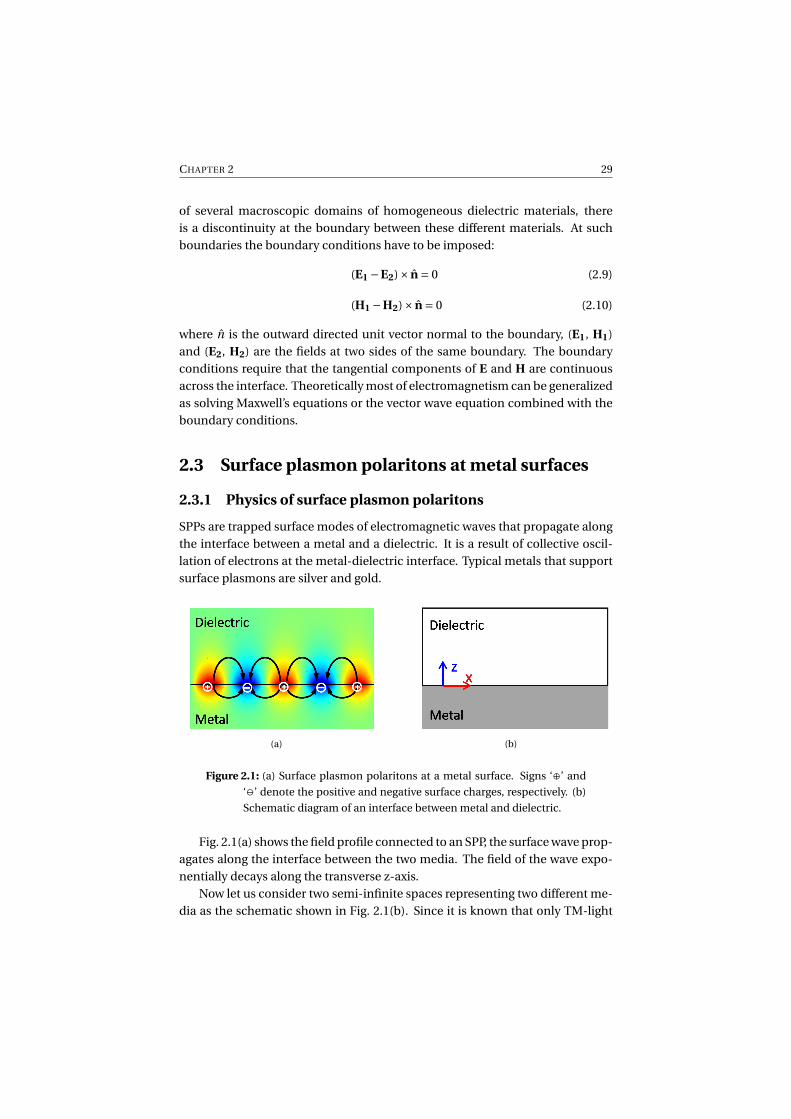
CHAPTER 2 29
of several macroscopic domains of homogeneous dielectric materials, thereis a discontinuity at the boundary between these different materials. At suchboundaries the boundary conditions have to be imposed:
(E1 −E2)× n = 0 (2.9)
(H1 −H2)× n = 0 (2.10)
where n is the outward directed unit vector normal to the boundary, (E1, H1)and (E2, H2) are the fields at two sides of the same boundary. The boundaryconditions require that the tangential components of E and H are continuousacross the interface. Theoretically most of electromagnetism can be generalizedas solving Maxwell’s equations or the vector wave equation combined with theboundary conditions.
2.3 Surface plasmon polaritons at metal surfaces
2.3.1 Physics of surface plasmon polaritons
SPPs are trapped surface modes of electromagnetic waves that propagate alongthe interface between a metal and a dielectric. It is a result of collective oscil-lation of electrons at the metal-dielectric interface. Typical metals that supportsurface plasmons are silver and gold.
(a) (b)
Figure 2.1: (a) Surface plasmon polaritons at a metal surface. Signs ‘⊕’ and
‘ª’ denote the positive and negative surface charges, respectively. (b)
Schematic diagram of an interface between metal and dielectric.
Fig. 2.1(a) shows the field profile connected to an SPP, the surface wave prop-agates along the interface between the two media. The field of the wave expo-nentially decays along the transverse z-axis.
Now let us consider two semi-infinite spaces representing two different me-dia as the schematic shown in Fig. 2.1(b). Since it is known that only TM-light

30 BACKGROUND
can excite surface plasmons, we assume a TM-polarized wave at these two do-mains given by [2]:
for z > 0, Hd = (0, Hyd , 0
)exp(i (kxd x +kzd z −ωt )) (2.11)
Ed = (Exd , 0, Ezd )exp(i (kxd x +kzd z −ωt )) (2.12)
for z < 0, Hm = (0, Hym , 0
)exp(i (kxm x +kzm z −ωt )) (2.13)
Em = (Exm , 0, Ezm)exp(i (kxm x +kzm z −ωt )) (2.14)
where the wavevector components satisfy:
k2xd +k2
zd = εd k20 (2.15)
k2xm +k2
zm = εmk20 . (2.16)
Here εd and εm are the permittivities of dielectric and metal respectively, thewavevector k0 =ω/c = 2π/λ0, with λ0 is the vacuum wavelength.
The TM-polarized fields have to satisfy the Maxwell-Faraday equation(Eq. 2.1) and Ampère’s law (Eq. 2.2). Meanwhile these fields have to fulfil theboundary conditions (Eqs. 2.9 and 2.10). In this way, a dispersion relation be-tween the wavevector kspp along the propagation direction and the angularfrequency ω can be derived as:
k2spp = k2
xd = k2xm = ω2
c2
εdεm
εd +εm. (2.17)
By substituting into Eqs. 2.15 and 2.16, the normal component of thewavevector can also be obtained
k2zd = ω2
c2
ε2d
εd +εm(2.18)
k2zm = ω2
c2
ε2m
εd +εm. (2.19)
For simplicity we neglect the imaginary part of the permittivity of media.Therefore in order to have a confined wave that propagates along the interface,kspp has to be real and kspp > 0. This requires that the product and the sumof the permittivities of the two media have to be either both positive or bothnegative. Meanwhile the normal components of the wavevector (kzd and kzm)in these two media have to be purely imaginary values to confine the wave tothe surface. This can only be fulfilled if the sum of the permittivities is negative.Therefore we have the conditions for a bound and propagating interface wave

CHAPTER 2 31
as follows:
εd ·εm < 0, (2.20)
εd +εm < 0. (2.21)
Eqs. 2.20 and 2.21 require that one of the permittivities is negative, with anabsolute value larger than that of the other. Metals can fulfil this requirement.Especially for noble metals like Ag and Au the absolute value of the real part ofthe permittivity is larger than the imaginary part at optical frequencies. So inplasmonics noble metals are always the materials in consideration.
Since this bound mode is propagating along an interface, instead of beinglocalized in 3D, this surface plasmon is called a propagating surface plasmonpolartions (SPPs), to distinguish the localized one, which will be introduced insection 2.4.
Now assume the permittivity of the metal to be
εm = ε′m + iε′′m (2.22)
where ε′m and ε′′m are real values, with |ε′m | À ε′′m > 0 for most of the noble met-als like Ag and Au at optical frequencies. The permittivity of the dielectric isassumed to be a real value, εd > 0, with no loss. The wavevector of the SPP prop-agation constant, kspp , can also be expressed in the complex form k ′
spp + i k ′′spp ,
approximately given by:
k ′spp ≈
√ε′mεd
ε′m +εd
ω
c, (2.23)
k ′′spp ≈ k ′
sppε′′mεd
2ε′m(ε′m +εd
) . (2.24)
The real part k ′spp determines the SPP (effective) wavelength λspp , whereas the
imaginary part k ′′spp determines the propagation length.
Under the assumption |ε′m |À εd > 0, it is easy to find that
k ′spp ≈
√ε′mεd
ε′m +εd
ω
c>p
εdω
c= nd k0 = kd , and, (2.25)
λspp = 2π
k ′spp
≈√ε′m +εd
ε′mεdλ0 <λ0. (2.26)
Here kd is the wavevector in the dielectric. Eq. 2.25 implies a wavevector mis-match between light in the dielectric and SPP, which means the SPP cannot beexcited by free space light directly. Eq. 2.26 reveals that the SPP can shrink thewavelength compared to free space.

32 BACKGROUND
2.3.2 Excitation of SPPs at a metal surface
As revealed in the previous section the wavevector for a given wavelength invacuum λ0 has to increase a certain amount to couple into the SPP. There aremainly two methods, using grating couplers [3] or prism couplers [4, 5].
Grating coupler
Figure 2.2: Schematic diagram of grating coupler for SPP coupling.
When light hits a grating (grating constant p) at an angle θ0 (Fig. 2.2), lightwill be diffracted, giving rise to different diffraction orders. According to theBragg condition, one obtains for the N th order diffraction along the x axis [2, 6]:
kxN = nd k0 sinθ0 +NG , (2.27)
where N is an integer and the diffraction order, G is the grating vector along thex-axis and its magnitude is given by 2π/p. For a grating in a metal film if wechoose the incident angle and the integer N properly, the diffracted light cancouple with the SPP by satisfying the following condition:
kx = nd k0 sinθ0 +NG = Re(kg
spp)
. (2.28)
Here, kgspp denotes the SPP wavevector along the grating surface. Because of the
perturbation of the metal surface kgspp is different from the one at a plane inter-
face given by Eq. 2.17. However kgspp ≈ kspp if the perturbation is small, hence
together with Eq. 2.28 we can estimate the required grating constant, incidentangle and diffraction order.
For a larger perturbation the periodicity will introduce a bandgap into thesurface plasmon dispersion relation, when the period is equal to half the SPPwavelength, as seen in Fig. 2.3 (a). SPP photonic bandgaps have been observedin experiments [7–9]. The bandgap is formed by the splitting of the SPP intotwo modes with different symmetry as shown in Fig. 2.3 (b). The symmetrical
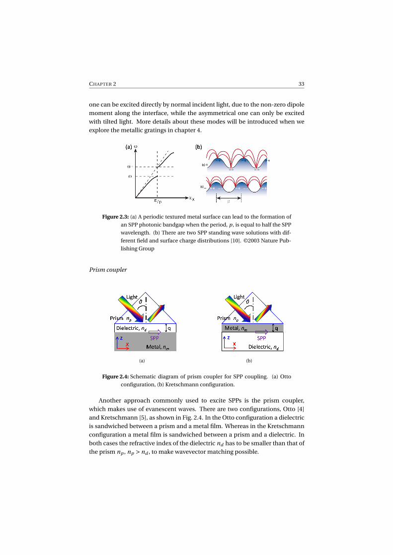
CHAPTER 2 33
one can be excited directly by normal incident light, due to the non-zero dipolemoment along the interface, while the asymmetrical one can only be excitedwith tilted light. More details about these modes will be introduced when weexplore the metallic gratings in chapter 4.
Figure 2.3: (a) A periodic textured metal surface can lead to the formation of
an SPP photonic bandgap when the period, p, is equal to half the SPP
wavelength. (b) There are two SPP standing wave solutions with dif-
ferent field and surface charge distributions [10]. ©2003 Nature Pub-
lishing Group
Prism coupler
(a) (b)
Figure 2.4: Schematic diagram of prism coupler for SPP coupling. (a) Otto
configuration, (b) Kretschmann configuration.
Another approach commonly used to excite SPPs is the prism coupler,which makes use of evanescent waves. There are two configurations, Otto [4]and Kretschmann [5], as shown in Fig. 2.4. In the Otto configuration a dielectricis sandwiched between a prism and a metal film. Whereas in the Kretschmannconfiguration a metal film is sandwiched between a prism and a dielectric. Inboth cases the refractive index of the dielectric nd has to be smaller than that ofthe prism np , np > nd , to make wavevector matching possible.
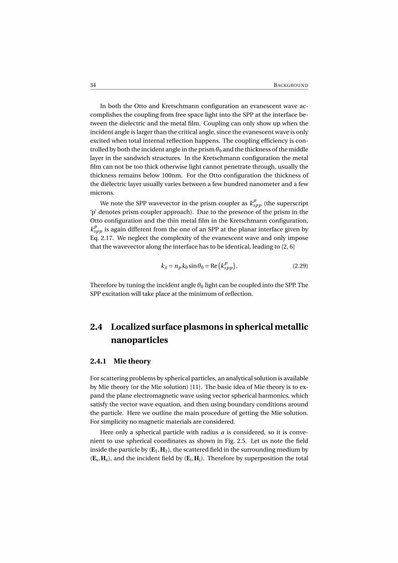
34 BACKGROUND
In both the Otto and Kretschmann configuration an evanescent wave ac-complishes the coupling from free space light into the SPP at the interface be-tween the dielectric and the metal film. Coupling can only show up when theincident angle is larger than the critical angle, since the evanescent wave is onlyexcited when total internal reflection happens. The coupling efficiency is con-trolled by both the incident angle in the prism θ0 and the thickness of the middlelayer in the sandwich structures. In the Kretschmann configuration the metalfilm can not be too thick otherwise light cannot penetrate through, usually thethickness remains below 100nm. For the Otto configuration the thickness ofthe dielectric layer usually varies between a few hundred nanometer and a fewmicrons.
We note the SPP wavevector in the prism coupler as kpspp (the superscript
‘p’ denotes prism coupler approach). Due to the presence of the prism in theOtto configuration and the thin metal film in the Kretschmann configuration,kp
spp is again different from the one of an SPP at the planar interface given byEq. 2.17. We neglect the complexity of the evanescent wave and only imposethat the wavevector along the interface has to be identical, leading to [2, 6]
kx = np k0 sinθ0 = Re(kp
spp)
. (2.29)
Therefore by tuning the incident angle θ0 light can be coupled into the SPP. TheSPP excitation will take place at the minimum of reflection.
2.4 Localized surface plasmons in spherical metallic
nanoparticles
2.4.1 Mie theory
For scattering problems by spherical particles, an analytical solution is availableby Mie theory (or the Mie solution) [11]. The basic idea of Mie theory is to ex-pand the plane electromagnetic wave using vector spherical harmonics, whichsatisfy the vector wave equation, and then using boundary conditions aroundthe particle. Here we outline the main procedure of getting the Mie solution.For simplicity no magnetic materials are considered.
Here only a spherical particle with radius a is considered, so it is conve-nient to use spherical coordinates as shown in Fig. 2.5. Let us note the fieldinside the particle by (E1,H1), the scattered field in the surrounding medium by(Es,Hs), and the incident field by (Ei,Hi). Therefore by superposition the total

CHAPTER 2 35
Figure 2.5: Spherical particle (radius a) with spherical coordinates.
field (E2,H2) in the surrounding medium is given by
E2 = Ei + Es (2.30)
H2 = Hi + Hs (2.31)
The electric and magnetic field components of an incident plane wave can beexpressed as
Ei = E0e i kr cosθêx (2.32)
Hi = k
ωµ0E0e i kr cosθêy (2.33)
with E0 the amplitude of the incident electric field at z = 0, k and ω are thewave vector and the frequency of the incident plane wave respectively. µ is thepermeability in vacuum, r is the radial coordinate, êx and êy are the unit vectorin x and y direction. So in order to obtain the total field one needs to solve forthe scattered field.
By fourier transform, a scalar wave of any form can be expanded as a planewave series, which is expressed with harmonics (such as a function of cosine).Plane waves in cosine form are eigenfunction solutions of the homogeneouselectromagnetic wave equation in cartesian coordinates. Similarly in spheri-cal coordinates, one can also find eigenfunction solutions to the vector waveequation. These solutions are called vector spherical harmonics, M and N. Fordetails of the derivation of vector spherical harmonics we refer to Ref [11]. Asa consequence, mathematically any kind of wave may also be expressed as anexpansion of vector spherical harmonics in spherical coordinates.
A plane wave described by equations 2.32 and 2.33 can be expressed by vec-

36 BACKGROUND
tor spherical harmonics as [11]
Ei = E0
∞∑n=1
i n 2n +1
n (n +1)
(M(1)
o1n − i N(1)e1n
)(2.34)
Hi =− k
ωµE0
∞∑n=1
i n 2n +1
n (n +1)
(M(1)
e1n + i N(1)o1n
)(2.35)
By applying the boundary conditions
(Ei +Es −E1)×êr = (Hi +Hs −H1)×êr = 0 (2.36)
at the boundary between particle and surrounding, the scattered field Es and Hs
can be determined as
Es = E0
∞∑n=1
i n 2n +1
n (n +1)
(i an N(3)
e1n −bn M(3)o1n
)(2.37)
Hs = k
ωµE0
∞∑n=1
i n 2n +1
n (n +1)
(i bn N(3)
o1n +an M(3)e1n
)(2.38)
And for the internal fields:
E1 = E0
∞∑n=1
i n 2n +1
n (n +1)
(cn M(1)
o1n − i dn N(1)e1n
)(2.39)
H1 =− k1
ωµE0
∞∑n=1
i n 2n +1
n (n +1)
(dn M(1)
e1n + i cn N(1)o1n
)(2.40)
where superscripts (1) and (3) denote the use of first kind Bessel functions jn
and first kind Hankel functions h(1)n . Subscripts (e1n) and (o1n) are illustrated
in Ref [11]. Coefficients an , bn , cn and dn are
an = mψ(mx)ψ′n(x)−ψ(x)ψ′
n(mx)
mψ(mx)ξ′n(x)−ξ(x)ψ′n(mx)
(2.41)
bn = ψ(mx)ψ′n(x)−mψ(x)ψ′
n(mx)
ψ(mx)ξ′n(x)−mξ(x)ψ′n(mx)
(2.42)
cn = mψ(x)ξ′n(x)−mξ(x)ψ′n(x)
ψ(mx)ξ′n(x)−mξ(x)ψ′n(mx)
(2.43)
dn = mψ(x)ψ′n(x)−mξ(x)ψ′
n(x)
mψ(mx)ξ′n(x)−ξ(x)ψ′n(mx)
(2.44)
where the size parameter x and relative refractive index m are
x = ka = 2πns a
λ(2.45)
m = np
ns(2.46)
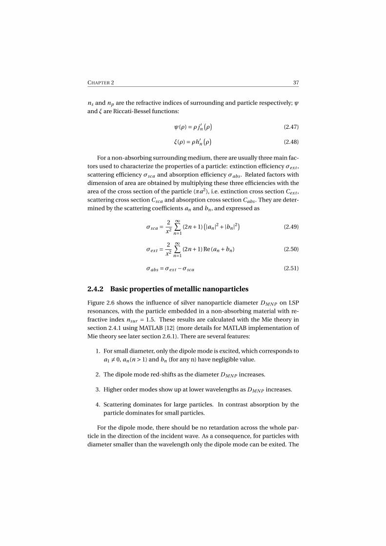
CHAPTER 2 37
ns and np are the refractive indices of surrounding and particle respectively; ψand ξ are Riccati-Bessel functions:
ψ(ρ) = ρ j ′n(ρ)
(2.47)
ξ(ρ) = ρh′n
(ρ)
(2.48)
For a non-absorbing surrounding medium, there are usually three main fac-tors used to characterize the properties of a particle: extinction efficiency σext ,scattering efficiency σsca and absorption efficiency σabs . Related factors withdimension of area are obtained by multiplying these three efficiencies with thearea of the cross section of the particle (πa2), i.e. extinction cross section Cext ,scattering cross section Csca and absorption cross section Cabs . They are deter-mined by the scattering coefficients an and bn , and expressed as
σsca = 2
x2
∞∑n=1
(2n +1)(|an |2 +|bn |2
)(2.49)
σext = 2
x2
∞∑n=1
(2n +1)Re(an +bn) (2.50)
σabs =σext −σsca (2.51)
2.4.2 Basic properties of metallic nanoparticles
Figure 2.6 shows the influence of silver nanoparticle diameter DM N P on LSPresonances, with the particle embedded in a non-absorbing material with re-fractive index nsur = 1.5. These results are calculated with the Mie theory insection 2.4.1 using MATLAB [12] (more details for MATLAB implementation ofMie theory see later section 2.6.1). There are several features:
1. For small diameter, only the dipole mode is excited, which corresponds toa1 6= 0, an(n > 1) and bn (for any n) have negligible value.
2. The dipole mode red-shifts as the diameter DM N P increases.
3. Higher order modes show up at lower wavelengths as DM N P increases.
4. Scattering dominates for large particles. In contrast absorption by theparticle dominates for small particles.
For the dipole mode, there should be no retardation across the whole par-ticle in the direction of the incident wave. As a consequence, for particles withdiameter smaller than the wavelength only the dipole mode can be exited. The

38 BACKGROUND
Figure 2.6: Influence of spherical silver nanoparticle size on LSP (calculated
with Mie theory in MATLAB). Green lines are the extinction efficien-
cies, red lines the absorption efficiencies, and blue lines the scattering
efficiencies.
dipole mode red-shifts to satisfy the no retardation requirement for larger par-ticles. When the diameter increases further and becomes comparable with thewavelength, a higher order quadrupole shows up (Fig. 2.6 (c)).
Figure 2.7 shows the dependence of the LSP resonance on the surround-ing media. Resonances red-shift as the surrounding refractive index increases.Therefore the LSP of metal nanoparticles is quite sensitive to the size of the par-ticle, and to the surrounding material (and also the particle shape, but here weonly consider spherical particles).
Figure 2.8 shows near-field distributions (normalized by the incident field)for different MNP sizes at resonance. Compared with larger particles, a strongerenhanced near-field can be observed for small ones. The retardation effects playan increasingly important role as the MNP size increases.

CHAPTER 2 39
Figure 2.7: Influence of surrounding medium on LSP of spherical silver
nanoparticles (calculated with Mie theory in MATLAB). Green lines
are the extinction efficiencies, red lines the absorption efficiencies,
and blue lines the scattering efficiencies.
For particles smaller than the wavelength, the fields in Eq. 2.37 and 2.38 canbe approximated by only including the a1 terms, yielding:
Es = E0
∞∑n=1
i n 2n +1
n (n +1)
(i an N(3)
e1n −bn M(3)o1n
)∼=−3
2E0a1N3
e1n ∝ E0
n2p −n2
s
n2p +2n2
s
(2.52)
where we see that the amplitude of Es reaches its maximum when
n2p +2n2
s = 0,or :
εp +2εs = 0.(2.53)
40 BACKGROUND
Figure 2.8: Electric field distributions normalized by the incident field for
spherical MNPs with different diameter at wavelengths correspond-
ing to peaks in Fig 2.6 (calculated with Mie theory in MATLAB). Plots
are across the center of the sphere. A plane wave is incident from the
top, and the incident E field is in plane to the plots. (a)–(c) correspond
to dipole modes for diameters of 10nm, 60nm and 100nm respectively,
(d) is the quadrupole mode for a diameter of 100nm.
Therefore for simplicity one can use Eq. 5.7 to estimate the position of an LSPresonance.
For non-spherical particles, the LSP resonance can be tuned by shape. TheLSP resonances of different shapes of Ag nanoparticles have been summarizedin [13], the LSP resonance can be tuned in a large wavelength range for differentapplications.
CHAPTER 2 41
2.4.3 Extended Mie theory
In the previously discussed classic Mie theory, the surrounding is assumed tobe non-absorbing, and only in this case the three efficiency factors (σext , σsca
and σabs ) are valid. In lossy media, the previous formulation for Mie theoryis still available only if we use the complex refractive index for the surround-ing medium [14–21], except that these three factors can not be used any longer.However based on extended Mie theory some interesting rigorous formulationscan be derived [18–21].
Let us consider an imaginary sphere with radius R (R > a) centered at theorigin (also the center of the particle) as shown in Fig. 2.5. The power thatcrosses the surface A of this imaginary sphere is given by the integral of thetime-averaged Poynting vector ⟨S⟩ over the surface A ("⟨⟩" denotes the time-average)
Wabs (R) =−∫
A⟨S⟩ ·êr d A
=−1
2Re
∫A
[(Ei +Es)× (
H∗i +H∗
s
)] ·êr d A
=−1
2Re
∫A
(Ei ×H∗
i
) ·êr d A− 1
2Re
∫A
(Es ×H∗
s
) ·êr d A
− 1
2Re
∫A
(Ei ×H∗
s +Es ×H∗i
) ·êr d A
=Wi −Wsca +Wext
(2.54)
where Wi is the incident power, Wsca the scattered power and Wext the crossterm. If Wabs > 0, energy is absorbed within the imaginary sphere.
Substituting the scattered field from Eqs. 2.37 and 2.38, and the incidentfield from Eqs. 2.34 and 2.35, we can get
Wi (R) =−1
2Re
∫A
(Ei ×H∗
i
) ·êr d A
= π|E0|2ωµ0
∞∑n=1
(2n +1)Im
(ψnψ
′∗n −ψ′
nψ∗n
k
) (2.55)
Wsca (R) = 1
2Re
∫A
(Es ×H∗
s
) ·êr d A
= π|E0|2ωµ0
∞∑n=1
(2n +1)Im
(|an |2ξ′nξ∗n −|bn |2ξnξ
′∗n
k
) (2.56)
42 BACKGROUND
Wext (R) =−1
2Re
∫A
(Ei ×H∗
s +Es ×H∗i
) ·êr d A
= π|E0|2ωµ0
∞∑n=1
(2n +1)
× Im
(a∗
nψ′nξ
∗n −b∗
nψnξ′∗n +anξ
′nψ
∗n −bnξnψ
′∗n
k
) (2.57)
Wabs (R) =Wi −Wsac +Wext
= π|E0|2ωµ0
∞∑n=1
(2n +1)
× Im
( (bnξn −ψn
)(b∗
nξ′∗n −ψ′∗
n
)− (anξ
′n −ψ′
n
)(anξ
∗n −ψ∗
n
)k
) (2.58)
Using the formulation above, one can calculate the absorption included in-side any sphere in a homogenous medium and other factors to investigate theinfluence of particles on the absorption in the surrounding [20, 21]. We willshow some studies based on this formulation for metallic nanoparticles in thenext chapter.
2.5 Localized surface plasmons of a nanowire
Many metallic nanostructures are explored and used in photonic applications,with nanowires being quite common. Therefore it is useful to theoretically an-alyze the LSP modes associated with a nanowire. We model the nanowire as aninfinitely long cylinder, provided that the aspect ratio is large enough. The anal-ysis procedure is similar to spherical particles, except that the wave equation issolved in cylindrical polar coordinates. In the following only the basic idea isoutlined. For simplicity the case with incidence direction and E-field polariza-tion perpendicular to the cylinder axis is considered. For more details readersare referred to [11].
Similarly, for the cylindrical case, vector cylindrical harmonics, Mn and Nn ,can be obtained [11]. We can represent the incident plane wave as an expansionof these harmonics [11]:
Ei =∞∑
n=−∞En N(1)
n (2.59)
Hi = −i k
ωµ
∞∑n=−∞
Hn M(1)n (2.60)

CHAPTER 2 43
Figure 2.9: Infinitely long cylinder with light incidence normal to its axis.
where En = E0(−i )n/k.
Meanwhile the solution inside the cylinder and for the scattered field is alsoexpanded:
Es =−∞∑
n=−∞En
(bn N(3)
n + i an M(3)n
)(2.61)
Hs = i k
ωµ
∞∑n=−∞
En(bn M(3)
n + i an N(3)n
)(2.62)
E1 =−∞∑
n=−∞En
(gn M(1)
n + fn N(1)n
)(2.63)
H1 = i k
ωµ
∞∑n=−∞
En(gn N(1)
n + fn M(1)n
)(2.64)
The final step is to couple these expansions together by applying the bound-ary conditions, in order to get the scattering coefficients. For the case we con-sider an vanishes, and bn becomes:
bn = Jn(mx)J ′n(x)−m J ′n(mx)Jn(x)
Jn(mx)H (1)′n (x)−m J ′n(mx)H (1)
n (x)(2.65)
where Jn and H (1)n are the first kind Bessel function and Hankel function.
For cylinders with a small diameter, one can also get a quasi-static approxi-mation to estimate the resonant wavelength of the LSP:
n2p +n2
s = 0,or :
εp +εs = 0.(2.66)
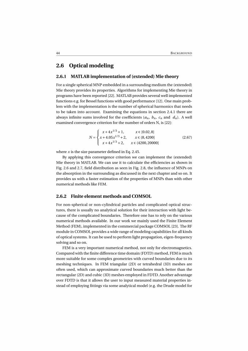
44 BACKGROUND
2.6 Optical modeling
2.6.1 MATLAB implementation of (extended) Mie theory
For a single spherical MNP embedded in a surrounding medium the (extended)Mie theory provides its properties. Algorithms for implementing Mie theory inprograms have been reported [22]. MATLAB provides several well implementedfunctions e.g. for Bessel functions with good performance [12]. One main prob-lem with the implementation is the number of spherical harmonics that needsto be taken into account. Examining the equations in section 2.4.1 there arealways infinite sums involved for the coefficients (an , bn , cn and dn). A wellexamined convergence criterion for the number of orders N, is [22]:
N =
x +4x1/3 +1, x ∈ [0.02,8]
x +4.05x1/3 +2, x ∈ (8,4200]
x +4x1/3 +2, x ∈ (4200,20000]
(2.67)
where x is the size parameter defined in Eq. 2.45.By applying this convergence criterion we can implement the (extended)
Mie theory in MATLAB. We can use it to calculate the efficiencies as shown inFig. 2.6 and 2.7, field distribution as seen in Fig. 2.8, the influence of MNPs onthe absorption in the surrounding as discussed in the next chapter and so on. Itprovides us with a faster estimation of the properties of MNPs than with othernumerical methods like FEM.
2.6.2 Finite element methods and COMSOL
For non-spherical or non-cylindrical particles and complicated optical struc-tures, there is usually no analytical solution for their interaction with light be-cause of the complicated boundaries. Therefore one has to rely on the variousnumerical methods available. In our work we mainly used the Finite ElementMethod (FEM), implemented in the commercial package COMSOL [23]. The RFmodule in COMSOL provides a wide range of modeling capabilities for all kindsof optical systems. It can be used to perform light propagation, eigen-frequencysolving and so on.
FEM is a very important numerical method, not only for electromagnetics.Compared with the finite difference time domain (FDTD) method, FEM is muchmore suitable for some complex geometries with curved boundaries due to itsmeshing techniques. In FEM triangular (2D) or tetrahedral (3D) meshes areoften used, which can approximate curved boundaries much better than therectangular (2D) and cubic (3D) meshes employed in FDTD. Another advantageover FDTD is that it allows the user to input measured material properties in-stead of employing fittings via some analytical model (e.g. the Drude model for
CHAPTER 2 45
optical constants used in FDTD). Since this work uses established FEM softwareto model solar cells, and does not develop a source code, here we only summa-rize the basic idea behind FEM for solving Maxwell’s equations.
Let us consider a 2D problem, the governing scalar Helmholtz equation in ahomogeneous medium is:
∇2φ+k2φ= 0. (2.68)
In solving for the primary unknown quantity φ under certain boundary condi-tions by FEM, the following general steps are involved:
• Discretization of the geometry under investigation, e.g. triangular mesh-ing as shown in Fig. 2.10(a);
(a) (b)
Figure 2.10: (a) Triangular mesh example in a model consisting of shapes of a
rectangle and a circle. (b) A single mesh element.
• Find proper interpolation functions (also called shape functions)φe , usu-ally a set of polynomials. The accuracy of the solution depends on the or-der of these polynomials, e.g. linear, quadratic or even higher orders. Herefor simplicity let us consider linear ones φe = a +bx + c y . In each trian-gular mesh element e, φe is interpolated based on the values at the nodesor those at edges, depending if nodal elements or edge elements are used.For a nodal element, φe at any point P inside element e (see Fig. 2.10(b))can be expressed as:
φe =3∑
i=1uiφei , (2.69)
where φei is the value of φe at nodes (the vertices of the mesh), ui isknown as a barycentric or area coordinate, a value dependent on the co-ordinates. Therefore to get the solution of the primary unknown quantityφ in the whole geometry domain, one only has to get the numerical solu-tion of its values at nodes.
46 BACKGROUND
• To get the numerical solution of φe , one converts the governing equa-tion Eq. 2.68 to an integro-differential formulation. Usually there are twomethods to do so, using a functional or the weighted-residual method.The functional F (φ) of the governing equation can be obtained by cal-culating the energy in the system under investigation from the Poyntingtheorem and one obtains here:
F (φ) =Ne∑
e=1
ÏAe
1
2
[(∂φe
∂x
)2
+(∂φe
∂y
)2
−k2φe
]d s, (2.70)
where Ne is the total number of mesh elements, Ae is the area of elemente. The weighted-residual method is obtained directly from the governingequation by transferring all terms of the equation on one side and thenmultiplying by a weight function we :
W (φ) =Ne∑
e=1
ÏAe
we(∇2φe +k2φe
)d s. (2.71)
By minimizing F (φ) or W (φ) one obtains a numerical solution of φe .
For more details involved in each step we refer to Ref. [24–26].
With FEM one obtains numerical solutions of field distributions (both elec-tric and magnetic) in optical systems such as OSCs. Based on these distribu-tions postprocessing can be performed to calculate parameters of interest. Toget accurate solutions the mesh is a very important issue. Usually the maximummesh size in the medium is determined as λ/6, where λ is the wavelength in thematerial. For some special cases in which the field intensity gradient is larger afiner mesh is necessary. For example LSPs and SPPs appear in a very small areaand decay very rapidly from the metal interfaces. For these cases a fine mesh onthe order of the skin depth has to be adopted along the interfaces. In general, tofind a proper mesh size one can always perform a convergence investigation.
In modeling it is often impossible to include the whole solar cell structure inthe computational domain. Certain techniques have to be applied to truncatethe OSC structure in computations. The RF module of COMSOL provides var-ious boundary conditions to reduce the computational domain. For instanceone can apply periodic boundary conditions to use only one unit cell of a peri-odic structure. There are other boundary conditions for symmetries available,such as perfect electric and magnetic conductors which force the electric andmagnetic field perpendicular to the boundaries, respectively. For cases withopen boundaries an important trick to reduce the model size is the perfectlymatched layer (PML). PML is an artificial absorbing layer enclosing the modelto absorb outgoing light from the model. In COMSOL a key point of using PMLis to set its material property the same as the one next to it.

CHAPTER 2 47
Another important issue is the setup of a light source which provides the in-put excitation. For an optical system enclosed in a homogeneous medium, likea MNP in air, one can use the scattered field formulation in COMSOL, in which aplane wave background field is applied. For an OSC with light illuminating fromair, the optically thick glass substrate is usually modeled as semi-infinite, omit-ting the bottom air/glass interface. In such a system the OSC is enclosed in twosemi-infinite media (the glass substrate and the air on the other side) insteadof in a single homogeneous medium. Therefore one has to use ‘port’ togetherwith ‘assembly’ in COMSOL to introduce a light source to the model. For moretechniques for light sources one is referred to the COMSOL documentation andonline forum [23].

48 BACKGROUND
References
[1] S. A. Maier. Plasmonics: Fundamentals and Applications. Springer Verlag,2007.
[2] H. Raether. Surface Plasmons on Smooth and Rough Surfaces and on Grat-ings. Springer, Berlin, 1988.
[3] R. H. Ritchie, E. T. Arakawa, J. J. Cowan, and R. N. Hamm. Surface-plasmon resonance effect in grating diffraction. Physical Review Letters,21(22):1530–1533, 1968.
[4] A. Otto. Excitation of nonradiative surface plasma waves in silver by themethod of frustrated total reflection. Zeitschrift für Physik A Hadrons andNuclei, 216(4):398–410, 1968.
[5] E. Kretschmann and H. Raether. Radiative decay of non radiative surfaceplasmons excited by light. Zeitschrift Fuer Naturforschung, Teil A, 23:2135,1968.
[6] J. Homola, editor. Surface Plasmon Resonance Based Sensors, volume 4.Springer Verlag, 2006.
[7] W. Barnes, T. Preist, S. Kitson, and J. Sambles. Physical origin of photonicenergy gaps in the propagation of surface plasmons on gratings. PhysicalReview. B, Condensed matter, 54(9):6227–6244, 1996.
[8] S. C. Kitson, W. L. Barnes, and J. R. Sambles. Full photonic band gap for sur-face modes in the visible. Physical Review Letters, 77(13):2670–2673, 1996.
[9] W. L. Barnes, S. C Kitson, T. W. Preist, and J. R. Sambles. Photonic surfacesfor surface-plasmon polaritons. Journal of Optical Society of America A,14(7):1654–1661, 1997.
[10] W. L. Barnes, A. Dereux, and T. W. Ebbesen. Subwavelength optics. Nature,424:824–830, 2003.
[11] C. F. Bohren and D. R. Huffman. Absorption and Scattering of Light by SmallParticles. John Wiley and Sons, New York, 1983.
[12] MATLAB. http://www.mathworks.com/.
[13] M. Rycenga, C. M. Cobley, J. Zeng, W. Li, C. H. Moran, Q. Zhang, D. Qin,and Y. Xia. Controlling the synthesis and assembly of silver nanostructuresfor plasmonic applications. Chemical Reviews, 111(6):3669–712, 2011.
CHAPTER 2 49
[14] W. C. Mundy, J. A. Roux, and A. M. Smith. Mie scattering by spheres in an ab-sorbing medium. Journal of the Optical Society of America. A, 64(12):1593–1597, 1974.
[15] P. Chýlek. Light scattering by small particles in an absorbing medium. Jour-nal of the Optical Society of America. A, 67(4):561–563, 1977.
[16] C. F. Bohren and D. P. Gilra. Extinction by a spherical particle in an absorb-ing medium. Journal of Colloid and Interface Science, 72(2):215–221, 1979.
[17] M. Quinten and J. Rostalski. Lorenz-Mie Theory for spheres immersed inan absorbing host medium. Particle and Particle Systems Characterization,13(2):89–96, 1996.
[18] A. N. Lebedev, M. Gartz, U. Kreibig, and O. Stenzel. Optical extinction byspherical particles in an absorbing medium: application to composite ab-sorbing films. The European Physical Journal D, 6(3):365–373, 1999.
[19] I. W. Sudiarta and P. Chylek. Mie-scattering formalism for spherical parti-cles embedded in an absorbing medium. Journal of the Optical Society ofAmerica A, 18(6):1275–8, 2001.
[20] L. Hu, X. Chen, and G. Chen. Surface-Plasmon Enhanced Near-BandgapLight Absorption in Silicon Photovoltaics. Journal of Computational andTheoretical Nanoscience, 5(11):2096–2101, 2008.
[21] J. Y. Lee and P. Peumans. The origin of enhanced optical absorption in solarcells with metal nanoparticles embedded in the active layer. Optics Express,18(10):10078–87, 2010.
[22] W. J. Wiscombe. Improved Mie scattering algorithms. Applied Optics,19(9):1505–1509, 1980.
[23] Comsol Multiphysics. http://www.comsol.com.
[24] J. Jin. The Finite Element Method in Electromagnetics. John Wiley and Sons,New York, 1993.
[25] M. K. Haldar. Introducing the Finite Element Method in electromagneticsto undergraduates using MATLAB. International Journal of Electrical Engi-neering Education, 43(3):232–244, 2006.
[26] A. C. Polycarpou. Introduction to the Finite Element Method in Electromag-netics. Morgan & Claypool Publishers, 2005.

3Metallic nanoparticles
3.1 Introduction
Organic solar cells (OSCs) are of great current interest as they have a strong po-tential to reduce the cost of photovoltaics [1]. However, OSCs still have low ef-ficiency, up to 10.6% [2], due to the short exciton diffusion length, low chargemobility, limited absorption band and energy levels of polymers. This efficiencyis much smaller than for commercial silicon-based solar cells. The short excitondiffusion length in OSCs limits the thickness of the active layer. The advancedBHJ concept was introduced to solve the diffusion length problem and to keepthe required thickness of the active layer for sufficient light absorption [3].
However, in spite of using a BHJ, the thickness cannot be too large. Abovea certain thickness the conversion efficiency drops because free carrier recom-bination becomes significant [4]. Meanwhile increased internal resistance withthickness will yield a low filling factor. Several approaches have been proposedand reported to overcome weak absorption of OSCs: folded structures [5], tan-dem cell architectures [6–8], new materials for the active layer [9, 10], and metal-lic nanoparticles (MNPs) [6, 8, 11–14, 14–21].
Metallic nanoparticles tend to excite LSPs, with possibly a very strong scat-tering or near-field enhancement. From Mie theory, as explained in the pre-vious chapter, section 2.4.2, one finds that for particles with size smaller thanaround 30nm, the near-field enhancement dominates [22] since only the dipole
52 CHAPTER 3
mode is supported. For particles with size larger than 50nm the scattering ef-fect is more significant [23, 24]. For larger particles with size comparable to thewavelength retardation will come into effect, so that the higher order modescan be excited. Consequently the scattering effects dominate. The differentsize regimes point to two different ways to take advantage of LSPs. First, thestrong scattering can be used to redirect light more horizontally into the activelayer. Second, we can use enhanced near-fields, so that light spends more timearound a particle.
Several experiments and numerical investigations on the influence of MNPsin inorganic solar cells have been performed [23, 25–37]. In these studies largeMNPs are very often used and placed on top of the cells. The main idea is to en-hance the light path by exploiting the large forward scattering from MNPs andthe guided modes and other effects in the active layer. These cells have layerswith thicknesses e.g. in the range of micrometers (for Si thin-film) or ∼ 300nm(for amorphous Si), which are compatible with the larger diameter particles de-manded for efficient scattering. In addition, these thicker solar cell materialshave a lower, wide-band absorption, compared to organic materials.
There were also experiments and simulations conducted to investigate theinfluence of MNPs on OSCs. Usually in these investigations MNPs were embed-ded between the anode and the active layer [11–14], between tandem cells [6, 8],between active layer and cathode [14], or inside the active layer [15, 17–21]. Inmany experiments the particles tend to be incorporated inside the cells, andusually only have a size on the order of 10nm, which is limited by the thin thick-ness of layers demanded for good internal efficiency. As a result this makes theutilization of the prominent scattering of MNPs with large particles difficult.Therefore absorption and efficiency enhancements observed in these experi-ments should be mainly attributed to the near-field effects. Indeed, as shownlater, incorporating MNPs in the buffer layer (usually PEDOT:PSS) is not thatpromising from the optics viewpoint.
For small particles only the near-field effects with the dipole mode form apotential for light harvesting. They can only be effective when incorporatinginside the active layer. There are some recent reports about embedding silvernanoparticles directly or partially into the active layer [5, 9, 10, 18, 19]. Thesetypes of configurations can lead to very good absorption enhancement factors,however provided that the active layer is very thin, about 30–50nm thick [21].Therefore, we are mainly driven towards near-field enhancement, leading tostrong optical fields in the neighborhood of small particles. However recentlyreports on large MNPs have also shown its promising potential to boost the ef-ficiency [38].
In this chapter we address optical aspects in using MNPs to enhance theefficiency of OSCs by means of Finite Element Method (FEM). These problems

METALLIC NANOPARTICLES 53
concern such as which metal is the most promising candidate, where should theMNPs be embedded, what mechanism is behind the efficiency enhancementand so on. First in section 3.2 a single particle is studied to illustrate some ba-sic properties of MNPs in absorbing media using Mie theory. In the next threesections, 3.3, 3.4 and 3.5, we will exploit the near-field of MNPs for efficiencyenhancements of OSCs. In section 3.3, we reduce the 3D problem to a 2D one,since simulations have shown that a 2D model can give similar results to a 3Dmodel [39]. The advantages of this reduction are of course computational time-and memory saving, and it allows us to investigate a larger parameter space inmore detail. We discuss where the nanowire array should be embedded andhow different parameters of the MNP array affect the enhancement. In additionwe investigate the enhancement mechanism and analyze the absorption spec-tra in detail. In section 3.4 based on a 3D model we discuss the MNP materialchoice. In section 3.5, experiments from co-workers together with simulationsare presented for Ag islands covered by two different organic materials, CuPcand SubPc respectively. In section 3.6 strong scattering by larger particles is in-vestigated, in order to investigate this alternative approach.
3.2 A single spherical particle
Several different metals (Ag, Au, Al...) have been studied for plasmonic photo-voltaic applications. Figure 3.1 shows the permittivities of Ag, Au and Al [40].For bulk metal Ag and Al have lower loss in the visible light range compared toAu, the loss in a thick metal film is shown in Fig. 3.2(a). Ag has interband transi-tions (leading to absorption losses) only for low wavelengths (below ∼ 350nm)which means that at higher wavelengths the losses for Ag are relatively small.For Au the loss is significant below ∼ 550nm due to two interband transitions at∼ 330nm and ∼ 470nm. (The interband transitions also play an important rolein determining the plasmonic modes in MNPs.) However the loss in Al overridesAg and Au at large wavelengths.
Now we consider a spherical NP surrounded by an absorbing medium, thesame configuration as illustrated in Fig. 2.5. The surrounding is assumed tohave a refractive index 2+0.1i across the whole visible light range (a time de-pendence of e−iωt used to be consistent with Mie theory discussed previously),which is typically the refractive index of a polymer or small molecule material.To calculate the absorbed power, Wabs (R), in the surrounding material insidean arbitrary imaginary sphere with a radius of R, the extended Mie theory canbe applied. Therefore we define a figure of merit, absorption enhancement(AE), to assess the improvement of light harvesting in the absorbing surround-
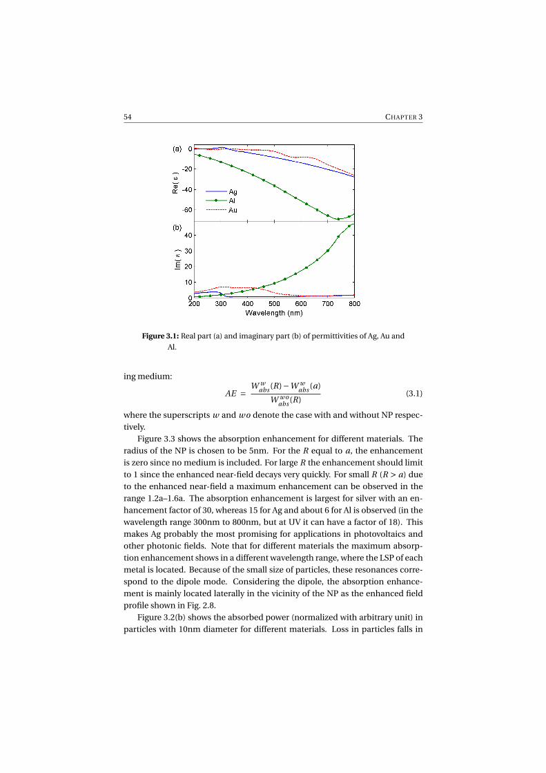
54 CHAPTER 3
Figure 3.1: Real part (a) and imaginary part (b) of permittivities of Ag, Au and
Al.
ing medium:
AE = W wabs (R)−W w
abs (a)
W woabs (R)
(3.1)
where the superscripts w and wo denote the case with and without NP respec-tively.
Figure 3.3 shows the absorption enhancement for different materials. Theradius of the NP is chosen to be 5nm. For the R equal to a, the enhancementis zero since no medium is included. For large R the enhancement should limitto 1 since the enhanced near-field decays very quickly. For small R (R > a) dueto the enhanced near-field a maximum enhancement can be observed in therange 1.2a–1.6a. The absorption enhancement is largest for silver with an en-hancement factor of 30, whereas 15 for Ag and about 6 for Al is observed (in thewavelength range 300nm to 800nm, but at UV it can have a factor of 18). Thismakes Ag probably the most promising for applications in photovoltaics andother photonic fields. Note that for different materials the maximum absorp-tion enhancement shows in a different wavelength range, where the LSP of eachmetal is located. Because of the small size of particles, these resonances corre-spond to the dipole mode. Considering the dipole, the absorption enhance-ment is mainly located laterally in the vicinity of the NP as the enhanced fieldprofile shown in Fig. 2.8.
Figure 3.2(b) shows the absorbed power (normalized with arbitrary unit) inparticles with 10nm diameter for different materials. Loss in particles falls in
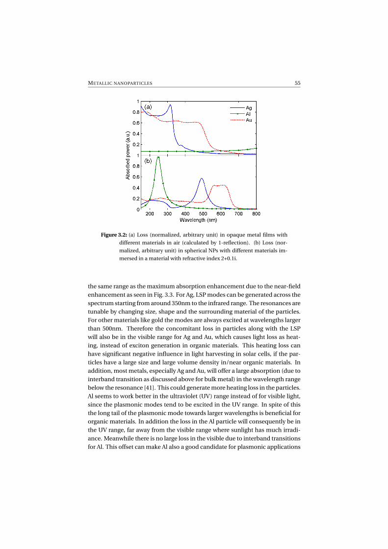
METALLIC NANOPARTICLES 55
Figure 3.2: (a) Loss (normalized, arbitrary unit) in opaque metal films with
different materials in air (calculated by 1-reflection). (b) Loss (nor-
malized, arbitrary unit) in spherical NPs with different materials im-
mersed in a material with refractive index 2+0.1i.
the same range as the maximum absorption enhancement due to the near-fieldenhancement as seen in Fig. 3.3. For Ag, LSP modes can be generated across thespectrum starting from around 350nm to the infrared range. The resonances aretunable by changing size, shape and the surrounding material of the particles.For other materials like gold the modes are always excited at wavelengths largerthan 500nm. Therefore the concomitant loss in particles along with the LSPwill also be in the visible range for Ag and Au, which causes light loss as heat-ing, instead of exciton generation in organic materials. This heating loss canhave significant negative influence in light harvesting in solar cells, if the par-ticles have a large size and large volume density in/near organic materials. Inaddition, most metals, especially Ag and Au, will offer a large absorption (due tointerband transition as discussed above for bulk metal) in the wavelength rangebelow the resonance [41]. This could generate more heating loss in the particles.Al seems to work better in the ultraviolet (UV) range instead of for visible light,since the plasmonic modes tend to be excited in the UV range. In spite of thisthe long tail of the plasmonic mode towards larger wavelengths is beneficial fororganic materials. In addition the loss in the Al particle will consequently be inthe UV range, far away from the visible range where sunlight has much irradi-ance. Meanwhile there is no large loss in the visible due to interband transitionsfor Al. This offset can make Al also a good candidate for plasmonic applications
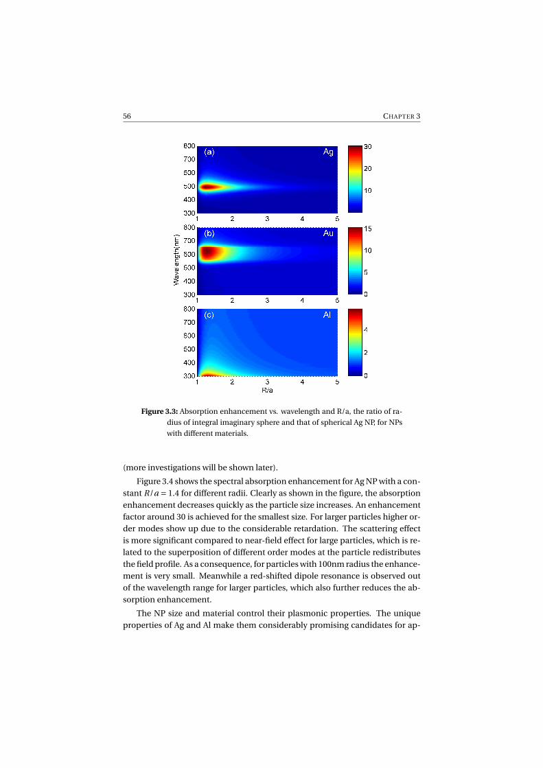
56 CHAPTER 3
Figure 3.3: Absorption enhancement vs. wavelength and R/a, the ratio of ra-
dius of integral imaginary sphere and that of spherical Ag NP, for NPs
with different materials.
(more investigations will be shown later).
Figure 3.4 shows the spectral absorption enhancement for Ag NP with a con-stant R/a = 1.4 for different radii. Clearly as shown in the figure, the absorptionenhancement decreases quickly as the particle size increases. An enhancementfactor around 30 is achieved for the smallest size. For larger particles higher or-der modes show up due to the considerable retardation. The scattering effectis more significant compared to near-field effect for large particles, which is re-lated to the superposition of different order modes at the particle redistributesthe field profile. As a consequence, for particles with 100nm radius the enhance-ment is very small. Meanwhile a red-shifted dipole resonance is observed outof the wavelength range for larger particles, which also further reduces the ab-sorption enhancement.
The NP size and material control their plasmonic properties. The uniqueproperties of Ag and Al make them considerably promising candidates for ap-

METALLIC NANOPARTICLES 57
Figure 3.4: Spectral absorption enhancement for Ag NPs with different radii
with R chosen to be 1.4a. The absorbing media has a refractive index
2+0.1i .
plication in photovoltaics. For small particles the near-field effects can be ex-ploited. For large particles the increased scattering effects could be used to dif-fuse the incident light into solar cells.
3.3 Nanowires
Based on the analytical studies in the previous section, here we exploit the near-field effects of Ag NPs to boost the light harvesting in OSCs. To start we considernanowire arrays which can be described by a simple 2D model. 3D sphericalparticles will be considered in the next section.
3.3.1 Simulation setup
In the simulations, due to the indium scarcity, an ITO-free structure [42] wasused as shown in Fig. 3.5. The Indium Tin Oxide (ITO) was replaced by a highlyconductive polymer, PEDOT:PSS with 20 nm thickness, which is a polymer withgood thermal and chemical stability and good flexibility. For the active layer thecommonly used polymer, P3HT:PCBM with 1:1 weight ratio was used. The ma-terial of the cathode is aluminum and the MNPs are silver. The material prop-erties of PEDOT:PSS, silver, aluminum and P3HT:PCBM are taken from litera-ture [5, 40, 43]. For the silver MNPs the influence of the free path effect [6, 44]on the dielectric constant is taken into account. Figure 3.6 shows the refractiveindices of the anode and the active material. For the active material the absorp-tion is mainly between 300nm and 650nm.

58 CHAPTER 3
Figure 3.5: Schematic figure of the model of the solar cell with MNPs. In sim-
ulations only the dotted domain is used.
Here we use a 2D model, so the MNPs are a periodic array of cylindricalnanowires, which are embedded in the middle of the active layer in all sim-ulations. Computations were performed using the commercial fully vectorialCOMSOL software package. Here in order to excite LSPs in the nanowires, lightwith electric field normal to the nanowires is normally incident from the air intothe solar cell (see Fig. 3.5), passing the PEDOT:PSS, the active layer and thenreaching the cathode. Some light is absorbed in the anode, the active layer andthe cathode, and the rest of it is reflected away from the solar cell.
Due to the periodicity and symmetry of the structure, by applying properboundary conditions to the vertical boundaries, only part of the solar cell con-taining half of the MNPs and half of the space between the MNPs is used, asshown by the dotted domain in Fig. 3.5. By this setting, we can save computermemory and computational time yet still give accurate results. In simulationsa mesh size of around 0.1 nm in the vicinity of the MNPs is employed. Compu-tations have been performed using monochromatic excitations over the wave-length interval 300–800nm.
The absorption spectrum ηA(λ) in each domain especially in active materialand MNPs can be calculated from the volume integral of the time average of thedivergence of the Poynting vector [45],
ηA(λ) =∫
∇· ⟨S⟩dV = 1
2Re
∫∇· (E×H∗)
dV = 1
2
∫ε′′ω|E|2dV , (3.2)
where E is the electric field distribution in the integrated volume, the ω is theangular frequency, and ε′′ is the imaginary part of the permittivity of the mate-rial in the integrated volume.
Since most of solar cells are usually characterized under AM 1.5G illumi-nation condition, the whole absorption, ηtot
A , in active layer over 300-800nm is

METALLIC NANOPARTICLES 59
Figure 3.6: Real part (a) and imaginary part (b) of refractive indices of PEDOT
and P3HT:PCBM(1:1).
calculated by means of integrating the absorption spectrum weighted by the AM1.5G solar spectrum, S(λ),
ηtotA =
∫ηA(λ)S(λ)dλ∫
S(λ)dλ. (3.3)
Another important metric is the short circuit current density, JSC . The JSC
achieves its maximum if we assume the internal quantum efficiency (ηIQE ) ofOSCs is 1, which means that all of the excitons are collected at electrodes andtransferred into photocurrent. OSCs with (ηIQE ) close to 100% have been dem-onstrated [46]. In this ideal case, the JSC is given by:
JSC = e∫
λ
hcηA(λ)S(λ)dλ. (3.4)

60 CHAPTER 3
where h is the Planck constant, c is the velocity of light in vacuum.
To evaluate the efficiency enhancement of OSCs by the MNPs we monitortwo metrics, the absorption enhancement and the current density enhance-ment. The absorption enhancement FA is a ratio of absorption in the activematerial with (w) MNPs to that without (wo) MNPs. The current density en-hancement F JSC is a ratio of current density with MNPs to that without MNPs.
FA = ηtot ,wA
ηtot ,woA
(3.5)
F JSC = J wSC
J woSC
(3.6)
3.3.2 Active layer thickness
As a benchmark, we first study solar cells without MNPs and investigate the in-fluence of the active layer thickness on the absorption. Theoretically, for a in-finite thick planar OSC without MNPs in the wavelength range 300–800nm themaximum of the absorption in the active layer is around 68.73% under AM 1.5Gillumination condition, given that no light is reflected back into free space andthe loss in anode PEDOT:PSS is negligible. Since the active material P3HT:PCBMonly absorbs light in the wavelength range from 300–650nm (as the absorptioncoefficient shows in Fig. 3.6). Figure 3.7 shows the absorption as a function ofthe active layer thickness. It can be seen that the absorption oscillates in func-tion of thickness due to interference effects (Fabry-Perot (FP) resonances) foractive layers thicker than 40nm. For thin active layers interference effects arenegligible, therefore the absorption in the active layer increases linearly withthe thickness. Maxima are observed at 61nm (50%), 196nm (59%) and 346nm(60%). From the inset of Fig. 3.7, it is clear that solar cells with 196nm activelayer can absorb almost all of the incident light over 300–650nm.
Clearly, thick active layers can absorb most of the incident light. However,as the thickness increases, carrier recombination will become significant whichreduces the internal quantum efficiency. Thin active layers have the advantagesof material-savings and a high carrier collection efficiency, but at the cost oflow light harvesting. However, for solar cells with thin active layers, the lightharvesting can be increased by introducing MNPs into the structure. In this wayby benefiting from the optical effects of MNPs, organic solar cells could combinethe advantages of thin and thick active layers, namely high carrier collectionefficiency and strong light harvesting, resulting in efficient cells.
In what follows, we investigate the influence of MNPs on absorption en-hancement for a thin active layer with a thickness of 33nm. The absorptionfor this thickness is 30%, and the absorption spectrum is shown in the inset of

METALLIC NANOPARTICLES 61
Figure 3.7: Thickness dependence of absorption in the active layer. The in-
set shows the absorption spectra for active layers with varying thick-
nesses.
Fig. 3.7.
3.3.3 Optimization
To optimize the structure with MNPs systematic studies have been carried outfor various spacings (or periods) and MNP diameters. The absorption enhance-ment is mapped in Fig. 3.8 (a). Within a broad spacing and diameter an en-hancement factor larger than 1.2 can be obtained, which means 20% more lightis absorbed compared with the reference OSC without MNPs with an activelayer thickness of 33nm. Absorption enhancement reaches its maximum, a fac-tor of 1.56, with optimized parameter values: a diameter of 24nm and a spacingof 40nm. Considering the electrical property the current density enhancementis also mapped in Fig. 3.8 (b) given that the internal efficiency is as high as 1. Thecurrent density enhancement has a maximal value of 1.63 with the same opti-mized parameters as the optimal absorption enhancement. With the optimizedparameters, the current density is enhanced from 6.7mA/cm2 to 10.9mA/cm2,whereas the absorption is from 30% to 47%.
Figure 3.9 shows the absorption spectrum and the spectral current densityfor the optimized solar cells with 24nm diameter MNPs and 40nm spacing. Forcomparison, we also plot the absorption spectra and the spectral current den-sities for solar cells without MNPs with thicknesses of 33nm and 61nm, respec-tively. We remark that the absorption spectrum of 33nm active layer with MNPsfits the spectrum of 61nm active layer without MNPs quite well. As a result theabsorptions of these cells with (47%) and without (50%) MNPs are similar. Sim-

62 CHAPTER 3
(a)
(b)
Figure 3.8: Map of absorption (FA) (a) and current density (FJSC ) (b) enhance-
ments with MNPs in the middle of the active layer (33nm thickness)
as a function of particle spacing and diameter. Both of them reach the
maximum for MNP with diameter 24nm and a spacing of 40nm be-
tween MNPs. The absorption is enhanced from 30% to 47%, with an
enhancement factor of 1.56. Whereas the current density is enhanced
from 6.7 mA/cm2 to 10.9 mA/cm2 with an enhancement factor of 1.63.
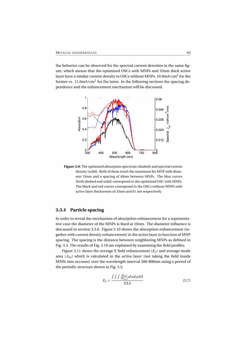
METALLIC NANOPARTICLES 63
ilar behavior can be observed for the spectral current densities in the same fig-ure, which means that the optimized OSCs with MNPs and 33nm thick activelayer have a similar current density to OSCs without MNPs, 10.9mA/cm2 for theformer vs. 11.6mA/cm2 for the latter. In the following sections the spacing de-pendence and the enhancement mechanism will be discussed.
Figure 3.9: The optimized absorption spectrum (dashed) and spectral current
density (solid). Both of them reach the maximum for MNP with diam-
eter 24nm and a spacing of 40nm between MNPs. The blue curves
(both dashed and solid) correspond to the optimized OSC with MNPs.
The black and red curves correspond to the OSCs without MNPs with
active layer thicknesses of 33nm and 61 nm respectively.
3.3.4 Particle spacing
In order to reveal the mechanism of absorption enhancement for a representa-tive case the diameter of the MNPs is fixed at 10nm. The diameter influence isdiscussed in section 3.3.6. Figure 3.10 shows the absorption enhancement (to-gether with current density enhancement) in the active layer in function of MNPspacing. The spacing is the distance between neighboring MNPs as defined inFig. 3.5. The results of Fig. 3.10 are explained by examining the field profiles.
Figure 3.11 shows the average E field enhancement (Ee ) and average modearea (Am) which is calculated in the active layer (not taking the field insideMNPs into account) over the wavelength interval 300-800nm using a period ofthe periodic structure shown in Fig. 3.5,
Ee =∫ ∫ ∫ |Ew |
|Ewo |d xd ydλ
S∆λ(3.7)

64 CHAPTER 3
Figure 3.10: Absorption and current density enhancements (FA and FJSC )
with MNPs (10nm diameter) in active layer as a function of particle
spacing.
Figure 3.11: Spacing dependence of average E field enhancement (solid line,
left y-axis) and average mode size (dashed line, right y-axis). The in-
sets show the E field enhancement at 425 nm with different spacings:
(a) 2 nm and (b) 20 nm.

METALLIC NANOPARTICLES 65
Am = 1
∆λ
∫ (∫ ∫ |Ew |2d xd y)2∫ ∫ |Ew |4d xd y
dλ (3.8)
where Ew and Ewo are the electric fields with and without MNPs in the activelayer, respectively. S denotes the area of active layer except that of MNPs. ∆λ isthe wavelength interval and corresponds to 500nm (from 300nm to 800nm).
Figure 3.10 shows that there exists an optimum spacing of 8nm maximizingthe absorption enhancement with a factor of around 1.48. This result is clari-fied by the graphs in Fig. 3.11. As the spacing increases, the electric field en-hancement gets smaller and smaller. However, the field enhancement beginsto spread out as the surface plasmon average mode area increases (also shownin Fig. 3.11). This is due to the decoupling between neighboring MNPs as illus-trated by the insets in Fig. 3.11. When MNPs are far away from each other, thestructure converges to the case with no MNPs, meaning that there is no absorp-tion enhancement. As a consequence of these competing effects, there exists anoptimum spacing.
3.3.5 Enhancement mechanism
In order to reveal which mechanism is more prominent, near-field enhance-ment or enhanced scattering, the active layer is divided into three sub-layers:front, middle and back sub-layers, as shown in the inset in Fig. 3.12(a). Fig-ure 3.12(a) shows the absorption spectra. Figure 3.12(b)-(e) depict E field en-hancement distributions (ratio of the |E| field with MNPs to that without MNPs)at representative wavelengths.
From Fig. 3.12 (a) one observes that the enhanced absorption is obvious onlyin the middle sub-layer where the MNPs are. The black dotted line has a broad-band enhancement in the range between around 385nm and 650nm. For theother two sub-layers enhanced absorption is only observed in small wavelengthranges while in other ranges the absorption is decreased. These phenomenaimply that the absorption enhancement is mainly attributed to near-field en-hancement, and not to enhanced scattering effects, which is consistent withMie results of section 3.2.
Figure 3.12(b)-(e) show the spatial distributions of the E field enhancementfor dips and peaks in the black dotted line in (a), at 330nm, 425nm, 485nm and565nm. At 330nm, due to the small Re(εAg ) at short wavelengths, silver losesits metallic properties, and no dipole-like resonance exists at these short wave-lengths. For 425nm, 485nm and 565nm, it is clear that the E field enhancementis mainly localized in the layer where the MNPs are. The maximum enhancedelectric field exists in the vicinity of the MNPs in the space between MNPs.Therefore, this also shows that the mechanism of absorption enhancement ismainly due to the enhanced near-field, and not to scattering.
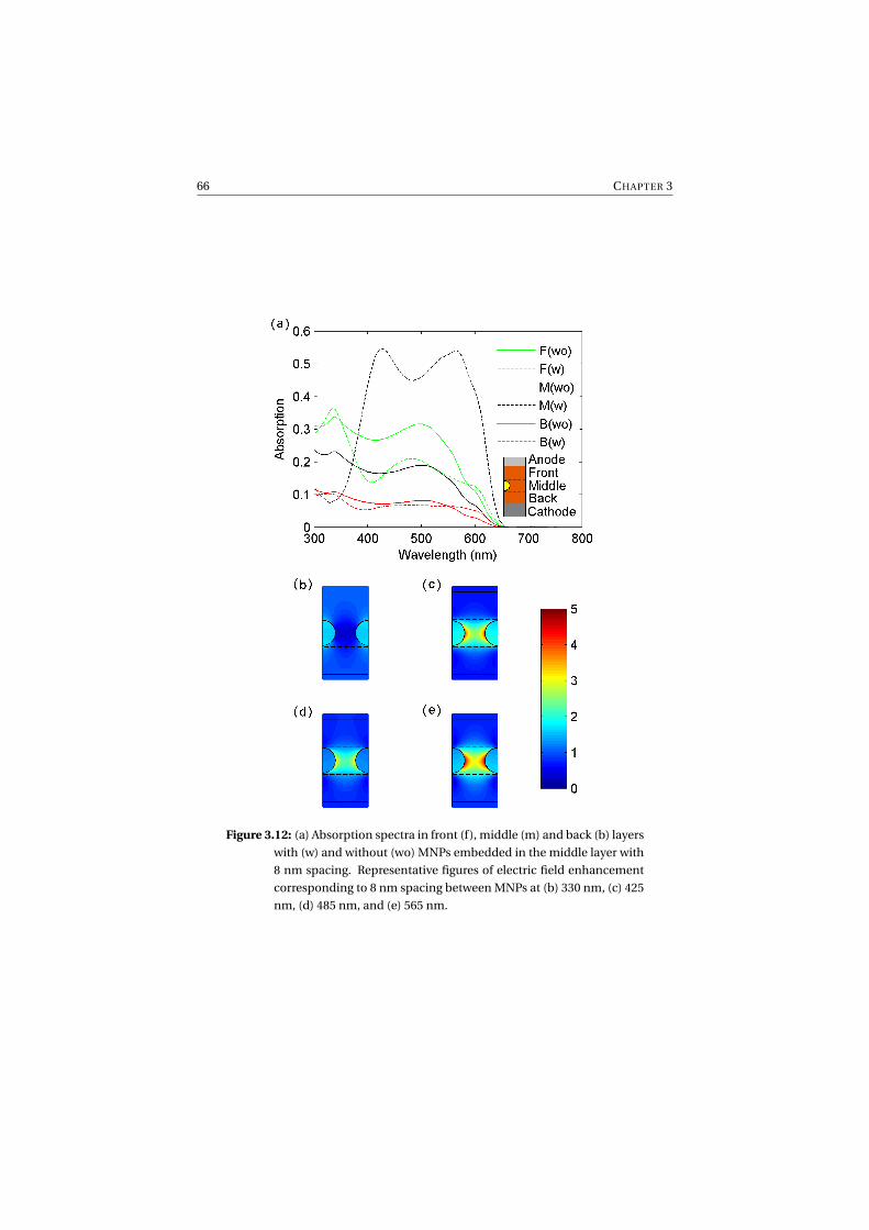
66 CHAPTER 3
Figure 3.12: (a) Absorption spectra in front (f), middle (m) and back (b) layers
with (w) and without (wo) MNPs embedded in the middle layer with
8 nm spacing. Representative figures of electric field enhancement
corresponding to 8 nm spacing between MNPs at (b) 330 nm, (c) 425
nm, (d) 485 nm, and (e) 565 nm.
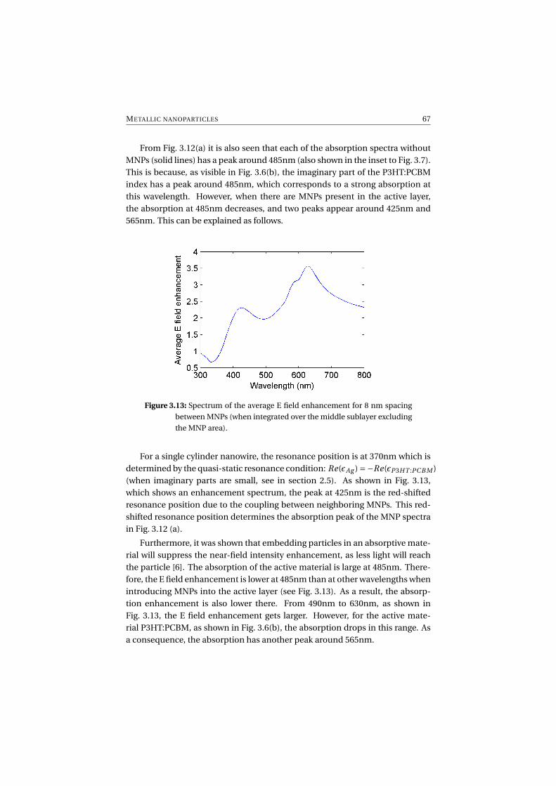
METALLIC NANOPARTICLES 67
From Fig. 3.12(a) it is also seen that each of the absorption spectra withoutMNPs (solid lines) has a peak around 485nm (also shown in the inset to Fig. 3.7).This is because, as visible in Fig. 3.6(b), the imaginary part of the P3HT:PCBMindex has a peak around 485nm, which corresponds to a strong absorption atthis wavelength. However, when there are MNPs present in the active layer,the absorption at 485nm decreases, and two peaks appear around 425nm and565nm. This can be explained as follows.
Figure 3.13: Spectrum of the average E field enhancement for 8 nm spacing
between MNPs (when integrated over the middle sublayer excluding
the MNP area).
For a single cylinder nanowire, the resonance position is at 370nm which isdetermined by the quasi-static resonance condition: Re(εAg ) =−Re(εP3HT :PC B M )(when imaginary parts are small, see in section 2.5). As shown in Fig. 3.13,which shows an enhancement spectrum, the peak at 425nm is the red-shiftedresonance position due to the coupling between neighboring MNPs. This red-shifted resonance position determines the absorption peak of the MNP spectrain Fig. 3.12 (a).
Furthermore, it was shown that embedding particles in an absorptive mate-rial will suppress the near-field intensity enhancement, as less light will reachthe particle [6]. The absorption of the active material is large at 485nm. There-fore, the E field enhancement is lower at 485nm than at other wavelengths whenintroducing MNPs into the active layer (see Fig. 3.13). As a result, the absorp-tion enhancement is also lower there. From 490nm to 630nm, as shown inFig. 3.13, the E field enhancement gets larger. However, for the active mate-rial P3HT:PCBM, as shown in Fig. 3.6(b), the absorption drops in this range. Asa consequence, the absorption has another peak around 565nm.
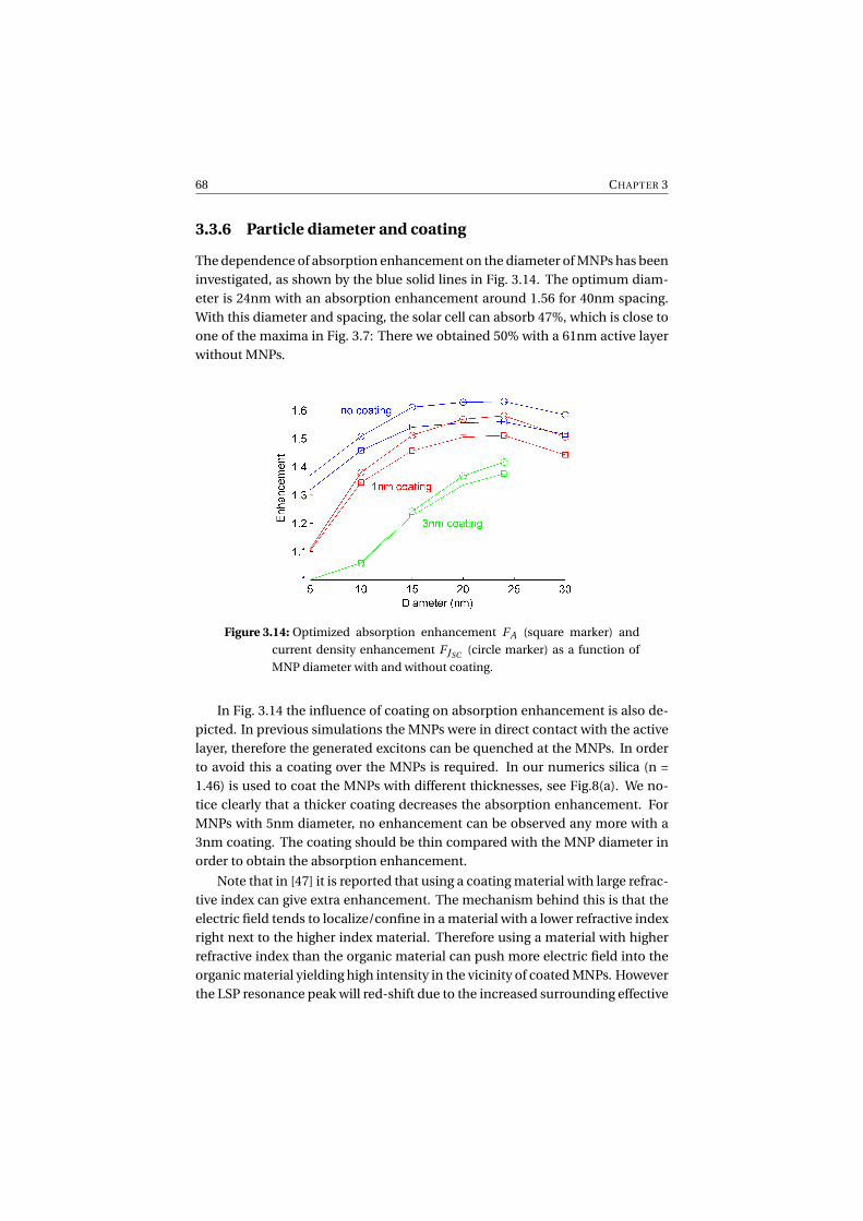
68 CHAPTER 3
3.3.6 Particle diameter and coating
The dependence of absorption enhancement on the diameter of MNPs has beeninvestigated, as shown by the blue solid lines in Fig. 3.14. The optimum diam-eter is 24nm with an absorption enhancement around 1.56 for 40nm spacing.With this diameter and spacing, the solar cell can absorb 47%, which is close toone of the maxima in Fig. 3.7: There we obtained 50% with a 61nm active layerwithout MNPs.
Figure 3.14: Optimized absorption enhancement FA (square marker) and
current density enhancement FJSC (circle marker) as a function of
MNP diameter with and without coating.
In Fig. 3.14 the influence of coating on absorption enhancement is also de-picted. In previous simulations the MNPs were in direct contact with the activelayer, therefore the generated excitons can be quenched at the MNPs. In orderto avoid this a coating over the MNPs is required. In our numerics silica (n =1.46) is used to coat the MNPs with different thicknesses, see Fig.8(a). We no-tice clearly that a thicker coating decreases the absorption enhancement. ForMNPs with 5nm diameter, no enhancement can be observed any more with a3nm coating. The coating should be thin compared with the MNP diameter inorder to obtain the absorption enhancement.
Note that in [47] it is reported that using a coating material with large refrac-tive index can give extra enhancement. The mechanism behind this is that theelectric field tends to localize/confine in a material with a lower refractive indexright next to the higher index material. Therefore using a material with higherrefractive index than the organic material can push more electric field into theorganic material yielding high intensity in the vicinity of coated MNPs. Howeverthe LSP resonance peak will red-shift due to the increased surrounding effective
METALLIC NANOPARTICLES 69
index. On this ground extra engineering should be performed to optimize thethickness and the material of the coating layer.
3.4 Nano-spheres
The previous OSC structure is sensitive to the light polarization, since only theTM polarized light can excite the LSP in metallic nanowires. For TE polariza-tion the MNP works as an absorber and will reduce light harvesting in the activelayer. Therefore the overall enhancement will be an average value of enhance-ments under these two polarizations. Here in this section periodic sphericalMNPs with square lattice embedded in solar cells will be investigated, which isnot very sensitive to the polarization under small incident angle. There are lotsof reported simulations and experiments on the utilization of Ag and Au nanos-tructures for light trapping in OSCs. Recently an increasing number of studieswith Al have been carried out. Compared to Ag and Au, Al is more cost-effectiveand also exhibits attractive plasmonic properties as discussed in section 3.2.Herein we will demonstrate these different materials from optical simulationaspects.
3.4.1 Embedded in the active layer
The structure of OSC investigated here is more concrete, including an ITOcoated glass substrate as illustrated in Fig. 3.15. The reflector is chosen to beAg. To have good internal quantum efficiency the P3HT:PCBM is determined tobe 40nm thick. Thicknesses of PEDOT:PSS and ITO layers are 20nm and 100nmrespectively. MNPs are embedded in the middle of the active layer. The glasssubstrate is taken as semi-infinite with light illuminating the structure fromglass.
Due to the polarization independence of the structure for normal incidence(in that an array of MNPs in a square lattice is used) only one polarization alongx-axis is considered. For unpolarized sunlight the absorption will be the sameas the polarized one since sunlight can be decomposed as two orthogonal po-larizations. Similar to the previous simulations, to save computational memoryand time, only quarter of one unit cell (one period) is modeled due to symmetryand periodicity of the structure. All the optical constants of P3HT:PCBM, PE-DOT:PSS and ITO used in simulations are measured by D. Cheyns at imec usinga SOPRA GESP-5 spectroscopic ellipsometer and are shown in Fig. 3.15(b).
Figure 3.16 shows the current density enhancement versus the diameter andthe ratio of spacing to diameter for Ag, Al and Au NPs. To have an intuitive com-parison these three enhancement maps utilize the same enhancement factorcolor scale with a maximum value of 1.5. Ag and Al have a comparable maximal

70 CHAPTER 3
Figure 3.15: (a) Schematic of OSCs with spherical Ag NPs array with square
lattice in active layer. (b) Refractive index of different materials.
Solid: n. Dash: k. Blue: P3HT:PCBM. Red: PEDOT:PSS. Green: ITO.
enhancement factor, 1.46 for Ag and 1.49 for Al, whereas we obtain only 1.09for Au. The current density has been boosted from 7.3mA/cm2 for referencestructure with no MNPs to 10.7mA/cm2 for OSCs with Ag NPs, 10.9mA/cm2
with Al NPs and 7.9mA/cm2 with Au NPs. Note that the map of current densityenhancement is very similar to the nanowire case as shown in Fig. 3.8(b) pre-viously. For a certain diameter the current density enhancement achieves itsmaximum at a ratio of spacing to diameter close to one. For smaller spacing theinteraction between particles is significant resulting in very localized near-fieldsin the small range between particles, similar to the nanowire case (section 3.3.4),making the enhancement small. For large spacing the enhancement decreasesdue to the near-field effects becoming negligible compared to the large domainof active material. The intermediate spacing provides an appropriate plasmonicmode volume to reach the enhancement maximum.
Figure 3.17 shows the optimized absorption spectra and spectral currentdensity of OSCs with MNPs together with that of the reference structure (with-out particles). Enhanced absorption is only observed above a certain wave-length. Au has the smallest enhanced range, while Al has the largest range andAg is in between. This is due to enhanced near-field along with the LSP exci-tation and the concomitant loss in MNPs. The near-field tends to enhance thelight harvesting above the resonance because its long tail tends to longer wave-lengths instead of towards shorter wavelengths 1. For Au and Ag the resonanceis located in the visible range (> 460nm for Ag and > 550nm for Au, the reso-nance will red-shift due to the coupling between the particles), whereas the Alone is located in UV. The reduction for Al at short wavelengths is due to the red-
1This is because the magnitude of the real part of the epsilon of metal increases with wavelengthas shown in Fig. 3.1.
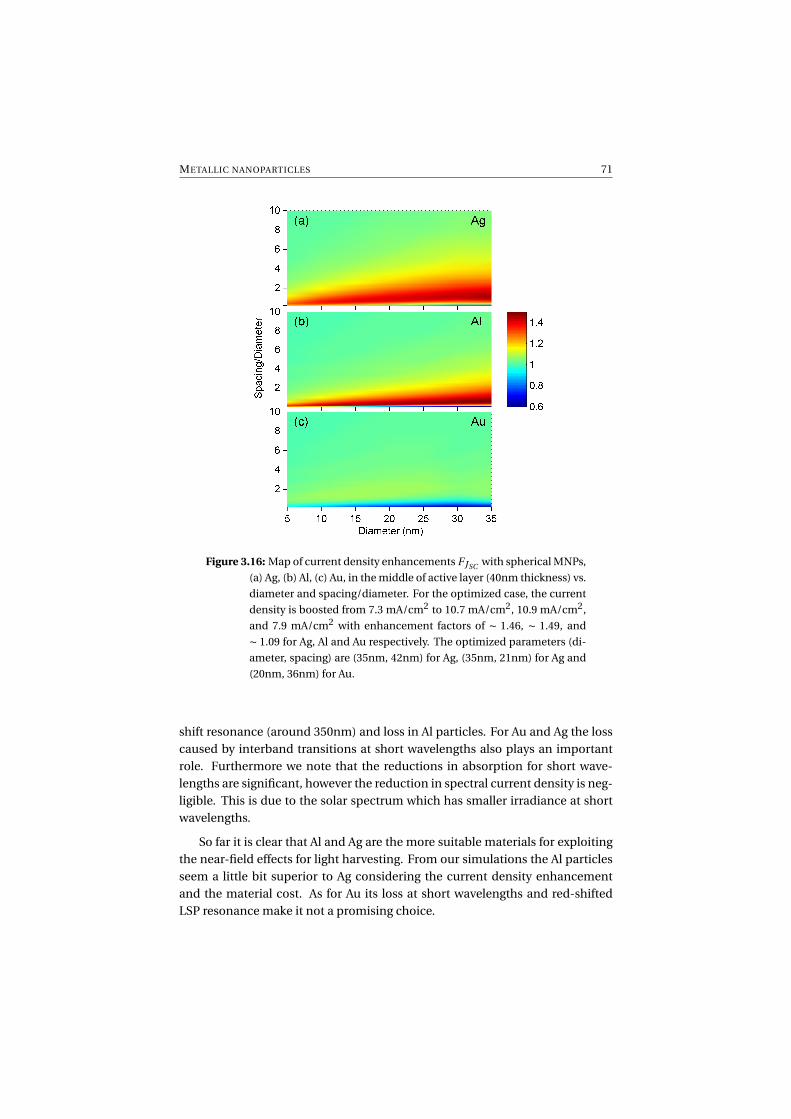
METALLIC NANOPARTICLES 71
Figure 3.16: Map of current density enhancements FJSC with spherical MNPs,
(a) Ag, (b) Al, (c) Au, in the middle of active layer (40nm thickness) vs.
diameter and spacing/diameter. For the optimized case, the current
density is boosted from 7.3 mA/cm2 to 10.7 mA/cm2, 10.9 mA/cm2,
and 7.9 mA/cm2 with enhancement factors of ∼ 1.46, ∼ 1.49, and
∼ 1.09 for Ag, Al and Au respectively. The optimized parameters (di-
ameter, spacing) are (35nm, 42nm) for Ag, (35nm, 21nm) for Ag and
(20nm, 36nm) for Au.
shift resonance (around 350nm) and loss in Al particles. For Au and Ag the losscaused by interband transitions at short wavelengths also plays an importantrole. Furthermore we note that the reductions in absorption for short wave-lengths are significant, however the reduction in spectral current density is neg-ligible. This is due to the solar spectrum which has smaller irradiance at shortwavelengths.
So far it is clear that Al and Ag are the more suitable materials for exploitingthe near-field effects for light harvesting. From our simulations the Al particlesseem a little bit superior to Ag considering the current density enhancementand the material cost. As for Au its loss at short wavelengths and red-shiftedLSP resonance make it not a promising choice.
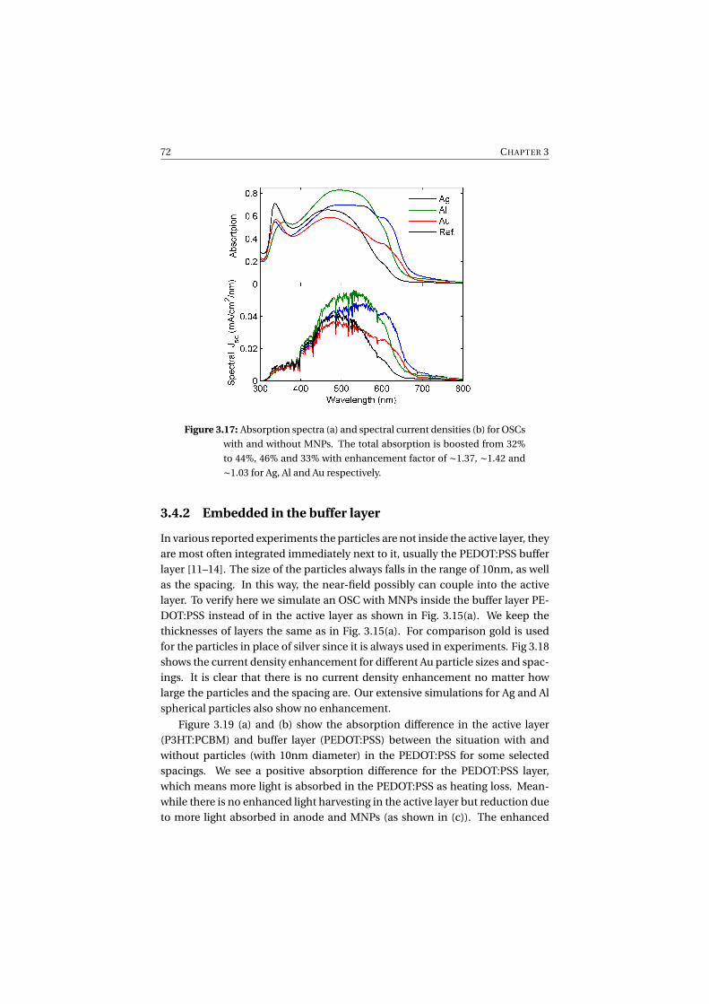
72 CHAPTER 3
Figure 3.17: Absorption spectra (a) and spectral current densities (b) for OSCs
with and without MNPs. The total absorption is boosted from 32%
to 44%, 46% and 33% with enhancement factor of ∼1.37, ∼1.42 and
∼1.03 for Ag, Al and Au respectively.
3.4.2 Embedded in the buffer layer
In various reported experiments the particles are not inside the active layer, theyare most often integrated immediately next to it, usually the PEDOT:PSS bufferlayer [11–14]. The size of the particles always falls in the range of 10nm, as wellas the spacing. In this way, the near-field possibly can couple into the activelayer. To verify here we simulate an OSC with MNPs inside the buffer layer PE-DOT:PSS instead of in the active layer as shown in Fig. 3.15(a). We keep thethicknesses of layers the same as in Fig. 3.15(a). For comparison gold is usedfor the particles in place of silver since it is always used in experiments. Fig 3.18shows the current density enhancement for different Au particle sizes and spac-ings. It is clear that there is no current density enhancement no matter howlarge the particles and the spacing are. Our extensive simulations for Ag and Alspherical particles also show no enhancement.
Figure 3.19 (a) and (b) show the absorption difference in the active layer(P3HT:PCBM) and buffer layer (PEDOT:PSS) between the situation with andwithout particles (with 10nm diameter) in the PEDOT:PSS for some selectedspacings. We see a positive absorption difference for the PEDOT:PSS layer,which means more light is absorbed in the PEDOT:PSS as heating loss. Mean-while there is no enhanced light harvesting in the active layer but reduction dueto more light absorbed in anode and MNPs (as shown in (c)). The enhanced
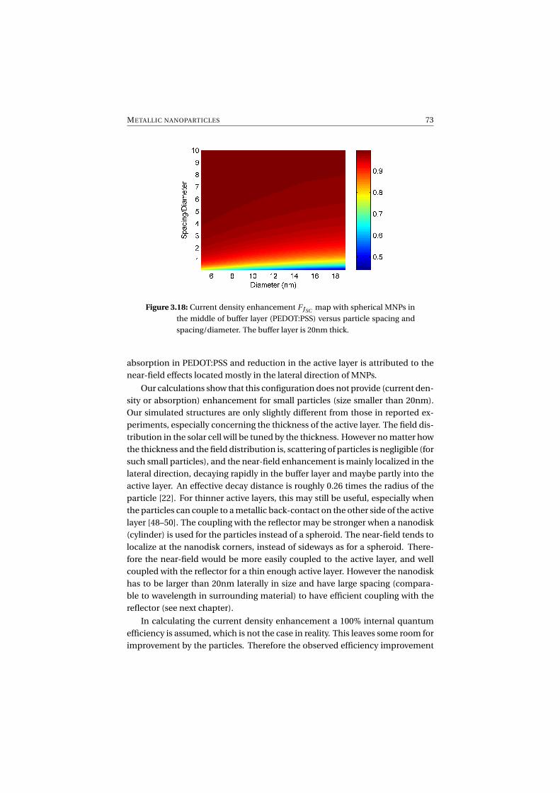
METALLIC NANOPARTICLES 73
Figure 3.18: Current density enhancement FJSC map with spherical MNPs in
the middle of buffer layer (PEDOT:PSS) versus particle spacing and
spacing/diameter. The buffer layer is 20nm thick.
absorption in PEDOT:PSS and reduction in the active layer is attributed to thenear-field effects located mostly in the lateral direction of MNPs.
Our calculations show that this configuration does not provide (current den-sity or absorption) enhancement for small particles (size smaller than 20nm).Our simulated structures are only slightly different from those in reported ex-periments, especially concerning the thickness of the active layer. The field dis-tribution in the solar cell will be tuned by the thickness. However no matter howthe thickness and the field distribution is, scattering of particles is negligible (forsuch small particles), and the near-field enhancement is mainly localized in thelateral direction, decaying rapidly in the buffer layer and maybe partly into theactive layer. An effective decay distance is roughly 0.26 times the radius of theparticle [22]. For thinner active layers, this may still be useful, especially whenthe particles can couple to a metallic back-contact on the other side of the activelayer [48–50]. The coupling with the reflector may be stronger when a nanodisk(cylinder) is used for the particles instead of a spheroid. The near-field tends tolocalize at the nanodisk corners, instead of sideways as for a spheroid. There-fore the near-field would be more easily coupled to the active layer, and wellcoupled with the reflector for a thin enough active layer. However the nanodiskhas to be larger than 20nm laterally in size and have large spacing (compara-ble to wavelength in surrounding material) to have efficient coupling with thereflector (see next chapter).
In calculating the current density enhancement a 100% internal quantumefficiency is assumed, which is not the case in reality. This leaves some room forimprovement by the particles. Therefore the observed efficiency improvement
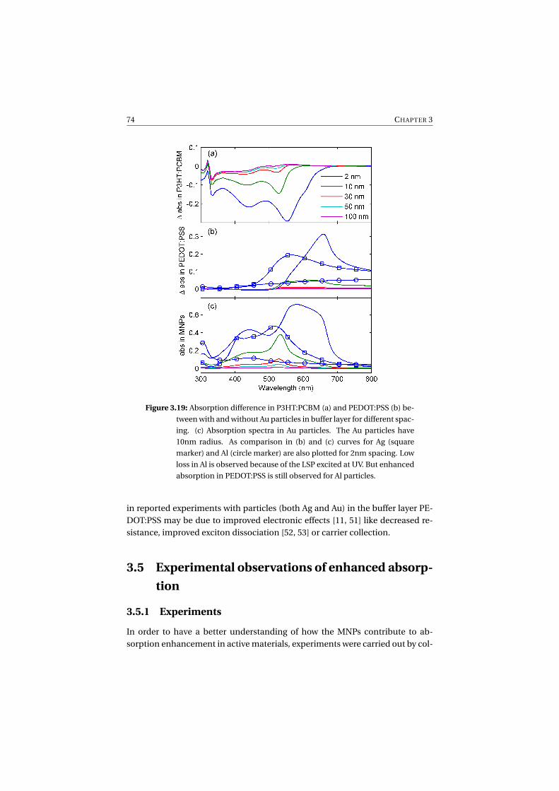
74 CHAPTER 3
Figure 3.19: Absorption difference in P3HT:PCBM (a) and PEDOT:PSS (b) be-
tween with and without Au particles in buffer layer for different spac-
ing. (c) Absorption spectra in Au particles. The Au particles have
10nm radius. As comparison in (b) and (c) curves for Ag (square
marker) and Al (circle marker) are also plotted for 2nm spacing. Low
loss in Al is observed because of the LSP excited at UV. But enhanced
absorption in PEDOT:PSS is still observed for Al particles.
in reported experiments with particles (both Ag and Au) in the buffer layer PE-DOT:PSS may be due to improved electronic effects [11, 51] like decreased re-sistance, improved exciton dissociation [52, 53] or carrier collection.
3.5 Experimental observations of enhanced absorp-
tion
3.5.1 Experiments
In order to have a better understanding of how the MNPs contribute to ab-sorption enhancement in active materials, experiments were carried out by col-
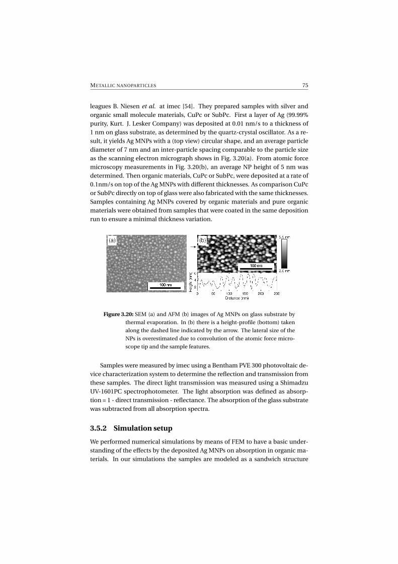
METALLIC NANOPARTICLES 75
leagues B. Niesen et al. at imec [54]. They prepared samples with silver andorganic small molecule materials, CuPc or SubPc. First a layer of Ag (99.99%purity, Kurt. J. Lesker Company) was deposited at 0.01 nm/s to a thickness of1 nm on glass substrate, as determined by the quartz-crystal oscillator. As a re-sult, it yields Ag MNPs with a (top view) circular shape, and an average particlediameter of 7 nm and an inter-particle spacing comparable to the particle sizeas the scanning electron micrograph shows in Fig. 3.20(a). From atomic forcemicroscopy measurements in Fig. 3.20(b), an average NP height of 5 nm wasdetermined. Then organic materials, CuPc or SubPc, were deposited at a rate of0.1nm/s on top of the Ag MNPs with different thicknesses. As comparison CuPcor SubPc directly on top of glass were also fabricated with the same thicknesses.Samples containing Ag MNPs covered by organic materials and pure organicmaterials were obtained from samples that were coated in the same depositionrun to ensure a minimal thickness variation.
Figure 3.20: SEM (a) and AFM (b) images of Ag MNPs on glass substrate by
thermal evaporation. In (b) there is a height-profile (bottom) taken
along the dashed line indicated by the arrow. The lateral size of the
NPs is overestimated due to convolution of the atomic force micro-
scope tip and the sample features.
Samples were measured by imec using a Bentham PVE 300 photovoltaic de-vice characterization system to determine the reflection and transmission fromthese samples. The direct light transmission was measured using a ShimadzuUV-1601PC spectrophotometer. The light absorption was defined as absorp-tion = 1 - direct transmission - reflectance. The absorption of the glass substratewas subtracted from all absorption spectra.
3.5.2 Simulation setup
We performed numerical simulations by means of FEM to have a basic under-standing of the effects by the deposited Ag MNPs on absorption in organic ma-terials. In our simulations the samples are modeled as a sandwich structure
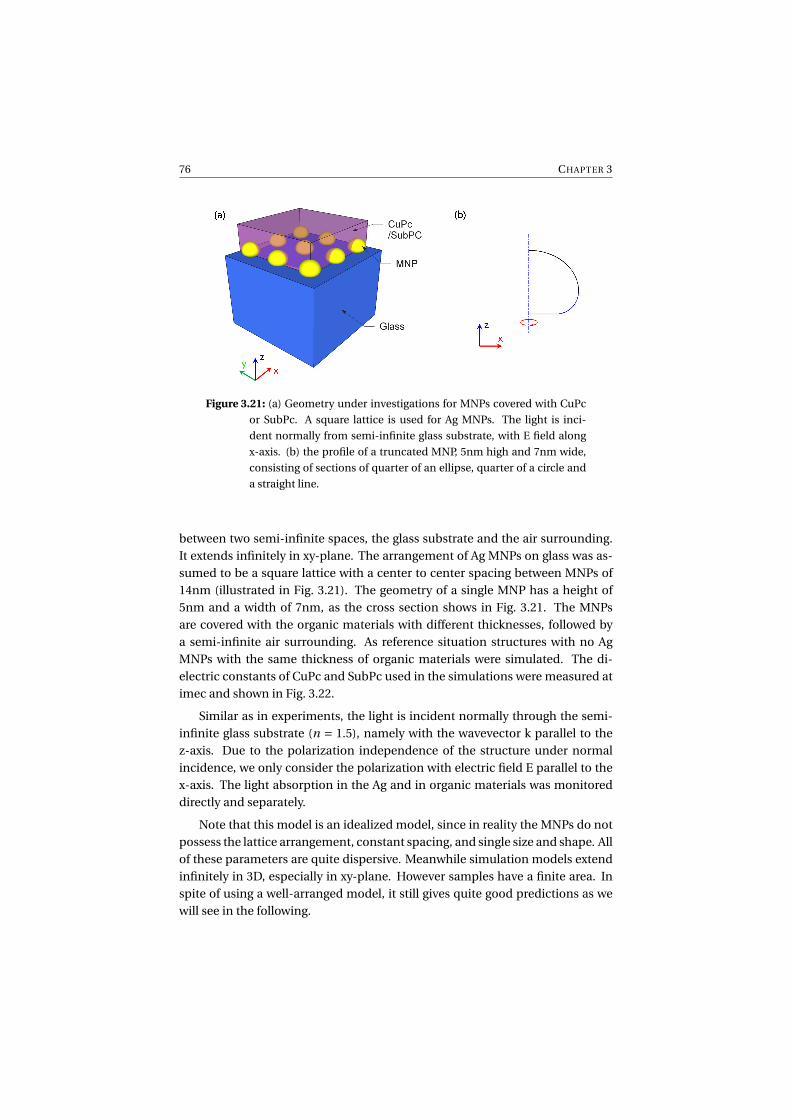
76 CHAPTER 3
Figure 3.21: (a) Geometry under investigations for MNPs covered with CuPc
or SubPc. A square lattice is used for Ag MNPs. The light is inci-
dent normally from semi-infinite glass substrate, with E field along
x-axis. (b) the profile of a truncated MNP, 5nm high and 7nm wide,
consisting of sections of quarter of an ellipse, quarter of a circle and
a straight line.
between two semi-infinite spaces, the glass substrate and the air surrounding.It extends infinitely in xy-plane. The arrangement of Ag MNPs on glass was as-sumed to be a square lattice with a center to center spacing between MNPs of14nm (illustrated in Fig. 3.21). The geometry of a single MNP has a height of5nm and a width of 7nm, as the cross section shows in Fig. 3.21. The MNPsare covered with the organic materials with different thicknesses, followed bya semi-infinite air surrounding. As reference situation structures with no AgMNPs with the same thickness of organic materials were simulated. The di-electric constants of CuPc and SubPc used in the simulations were measured atimec and shown in Fig. 3.22.
Similar as in experiments, the light is incident normally through the semi-infinite glass substrate (n = 1.5), namely with the wavevector k parallel to thez-axis. Due to the polarization independence of the structure under normalincidence, we only consider the polarization with electric field E parallel to thex-axis. The light absorption in the Ag and in organic materials was monitoreddirectly and separately.
Note that this model is an idealized model, since in reality the MNPs do notpossess the lattice arrangement, constant spacing, and single size and shape. Allof these parameters are quite dispersive. Meanwhile simulation models extendinfinitely in 3D, especially in xy-plane. However samples have a finite area. Inspite of using a well-arranged model, it still gives quite good predictions as wewill see in the following.

METALLIC NANOPARTICLES 77
Figure 3.22: Dielectric constants (n and k) of CuPc and SubPc. Black lines
for the n, blue for the k. Solids are the dielectric constants of CuPc,
dashes for SubPc.
3.5.3 Results
CuPc
To monitor the influence of MNPs on absorption in CuPc, the absorptiondifference ∆abs between samples with MNPs and without MNPs are investi-gated. In experiments the absorption difference ∆abs includes the absorptionin Ag MNPs since it is impossible to separate it. However in simulations this canbe done.
Figure 3.23(a) shows ∆abs from experiments and simulations. The solidlines show the simulated absorption difference with and without silver NPs inCuPc, including the loss in the silver NPs to correspond with measurements.We find that the measured and simulated results have similar curve profiles.For example, the main peaks are all showing up around 470nm in both simula-tions and experiments. These peaks correspond to the LSP resonance in smallAg MNPs, which can be verified by monitoring the absorption in Ag MNPs asshown in Fig. 3.23(b). Since the particle sizes are much smaller than the wave-length the peak position is directly determined by material properties, given bythe quasi-static approximation of Eq. 5.7 if one neglects the limited substrate ef-fects. However, the peaks in simulations are narrower than the measured ones.This could be due to:
1. The MNPs in simulations are periodically distributed, but in experimentthey are random;
2. The MNPs in simulations have the same size and shape, but in experiment

78 CHAPTER 3
Figure 3.23: (a) Absorption difference between samples with and without Ag
MNPs for different thicknesses of CuPc. Absorption in Ag MNPs is
included. Solids: simulations. Dashes: experiments. (b) Absorption
in Ag MNPs for different thicknesses of CuPc from simulations. The
absorption peak corresponds to the LSP resonance in Ag MNPs. (c)
Simulated absorption difference in CuPc between samples with and
without Ag MNPs for different thicknesses of CuPc.

METALLIC NANOPARTICLES 79
they have different sizes and shapes;
3. Slight influences might come from the infinite array in simulations com-pared with the finite sample area, and the absence of the glass-air inter-face on the incident side in simulations.
All of these aspects could broaden the resonance. As known the size, shape andspacing between particles can influence the LSP resonance. However the parti-cle size and shape of the sample will not vary a lot and the size is already quitesmall. Therefore among these aspects above distribution may be the most sig-nificant.
From Fig. 3.23(b) note that the absorption in Ag MNPs in the wavelengthrange 550nm–800nm is quite negligible. This implies the absorption differencein Fig. 3.23(a) in corresponding wavelength range is mostly attributed to CuPcin both experiments and simulations. Figure 3.23(c) shows the simulated ab-sorption difference in CuPc excluding the absorption in Ag MNPs. Enhancedabsorption can be observed for a broad wavelength range. The enhancementfor different thicknesses is quite constant in the vicinity of the resonance, whichis caused by the near-field enhancement around MNPs. However in the wave-length range larger than 550nm, the enhancement reduces quickly as the thick-ness increases. This can be understood because for a thicker organic layer, lessmaterial benefits from the near-field enhancement around MNPs.
SubPc
Figure 3.24 shows the results from simulations and experiments. Althoughagain absorption difference results from simulations are overestimated (Fig. 3.24(a)), they still have similar shapes. The two absorption peaks are well predictedby simulations. These two peaks are two dipole LSP resonances (as verified byabsorption in MNPs in Fig. 3.24(b)) in MNPs because the quite dispersive opti-cal refractive index of SubPc as shown in Fig. 3.22 (black dashed curve) resultsin two wavelengths that satisfy the quasi-static approximation for LSP dipoleresonance condition of Eq. 5.7. The broadened peaks should be due to the samereasons as listed previously. The absorption enhancement in SubPc (as shownin Fig. 3.24(a) and (c)) between these two peaks could be directly due to thenear-field enhancement, since the loss in Ag MNPs is quite small as shown inFig. 3.24(b).
Therefore as illustrated above by both simulations and experiments for twodifferent organic materials, Ag MNPs can enhance the absorption in the sur-rounded organic materials. The absorption enhancement is attributed to thenear-field enhancement from the dipole resonance in MNPs. Meanwhile theenhancement is not just limited to the resonance, but extends over larger wave-length range.

80 CHAPTER 3
Figure 3.24: (a) Absorption difference between sample with and without Ag
MNPs for different thickness of SubPc. Absorption in Ag MNPs is in-
cluded. Solids: simulations. Dashes: experiments. (b) Absorption in
Ag MNPs for different thickness of SubPc from simulations. The ab-
sorption peaks correspond to two LSP dipole resonances in Ag MNPs
located at different wavelength. (c)Simulated absorption difference
in SubPc between sample with and without Ag MNPs for different
thickness of SubPc.

METALLIC NANOPARTICLES 81
3.6 Large particles as scatterers
As shown in Fig. 3.4 the benefit for the absorbing medium from near-field effectsaround large particles is negligible. However it is possible to have the far-fieldbenefit of large particles, which is enhanced scattering. To exploit scattering itis not ideal to embed large particles directly in organic active materials, sincethe exciton diffusion length in organic materials is on the order of 10nm whichis small compared to the particle size. MNPs as scattering elements in Si thin-film solar cells have been demonstrated, and usually the particles are placed ontop of the solar cells [23, 25–37]. Here we present a feasibility study on MNPs asscatterers on top of OSCs. Figure 3.25 shows the structure under investigation.
Figure 3.25: Schematic diagram of Ag NP array as scatterers on top of ITO.
Light illuminates from the particle side.
To elucidate the basic principle behind MNPs as scatterers, we first exam-ine the properties of a single spherical Ag NP using Mie theory. In chapter 2 wehave already commented on this, here we provide a more detailed discussionon scattering. Figure 3.26 shows the scattering and absorption efficiencies fora Ag NPs with different diameters in an air surrounding. One sees that scatter-ing becomes more significant than absorption for larger particles, in additiona quadrupole mode is introduced. Notice that the absorption induced by thedipole mode is smaller than that by the quadrupole. Moreover as the particlesize increases the absorption and scattering are separated spectrally, yieldinga broadband enhancement scattering over the range where solar irradiance islarge. For instance the absorption and scattering are in the same wavelengthband for particle diameter 60nm, and the absorption is larger than scattering.Consequently for small particles they will work as absorbers rather than effi-cient scatterers in the configuration in Fig. 3.25. Therefore these results suggest

82 CHAPTER 3
that efficient scatterers have to be of large size.
Figure 3.26: (a) Scattering efficiency σsca and (b) absorption efficiency σabs
versus wavelength for a single Ag NP with different diameters (D).
The diamond marked purple line corresponds to the particle im-
mersed in a medium with refractive index 1.41, while others are in
air. DP: dipole mode. QP: quadrupole mode.
Now we examine the scenario depicted in Fig. 3.25. Here the thickness ofthe active layer P3HT:PCBM is fixed at 100nm, for the buffer layer PEDOT:PSS20nm, and for the ITO anode 100nm. The reflector is in Ag. The Ag NP arraywith square lattice is directly on top of the ITO. The reference structure is a pla-nar without particle array on top, which gives a total absorption of 44.7% in thewavelength range 300–800nm and a current density of 10.9mA/cm2. Light isnormally incident from the particle side, along the z-axis. We only consider po-larization with electric field parallel to the x-axis. The figures of merit are theabsorption and current density enhancement defined in Eqs. 3.5 and 3.6. Tooptimize the enhancement we investigate the particle diameter and the period(the lattice constant) of the array.
Figure 3.27 shows the period dependence of absorption and current densityenhancements for different diameters. Note that the maximum enhancementsincrease with particle diameter, in the range investigated here. This is becausethe scattering by an individual particle increases with diameter, as discussed
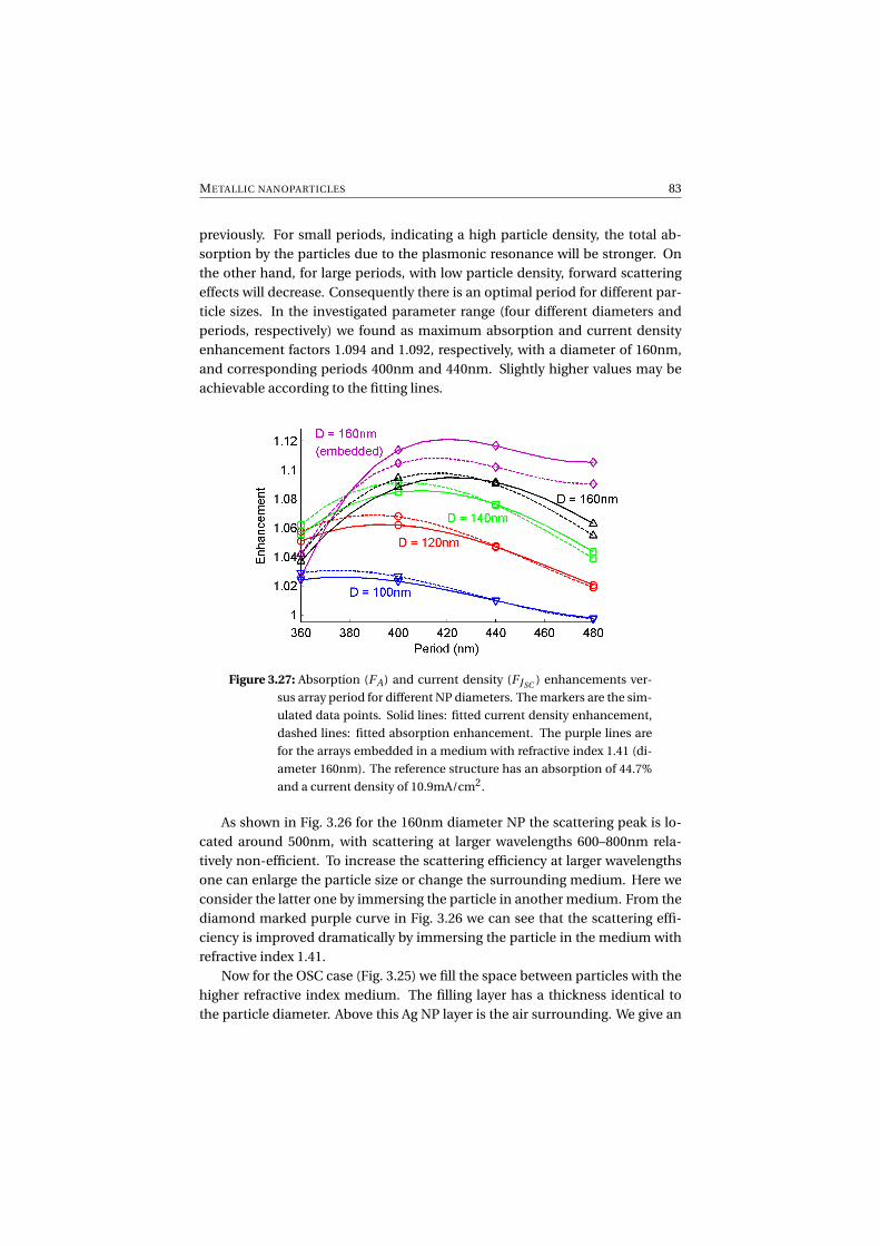
METALLIC NANOPARTICLES 83
previously. For small periods, indicating a high particle density, the total ab-sorption by the particles due to the plasmonic resonance will be stronger. Onthe other hand, for large periods, with low particle density, forward scatteringeffects will decrease. Consequently there is an optimal period for different par-ticle sizes. In the investigated parameter range (four different diameters andperiods, respectively) we found as maximum absorption and current densityenhancement factors 1.094 and 1.092, respectively, with a diameter of 160nm,and corresponding periods 400nm and 440nm. Slightly higher values may beachievable according to the fitting lines.
Figure 3.27: Absorption (FA) and current density (FJSC ) enhancements ver-
sus array period for different NP diameters. The markers are the sim-
ulated data points. Solid lines: fitted current density enhancement,
dashed lines: fitted absorption enhancement. The purple lines are
for the arrays embedded in a medium with refractive index 1.41 (di-
ameter 160nm). The reference structure has an absorption of 44.7%
and a current density of 10.9mA/cm2.
As shown in Fig. 3.26 for the 160nm diameter NP the scattering peak is lo-cated around 500nm, with scattering at larger wavelengths 600–800nm rela-tively non-efficient. To increase the scattering efficiency at larger wavelengthsone can enlarge the particle size or change the surrounding medium. Here weconsider the latter one by immersing the particle in another medium. From thediamond marked purple curve in Fig. 3.26 we can see that the scattering effi-ciency is improved dramatically by immersing the particle in the medium withrefractive index 1.41.
Now for the OSC case (Fig. 3.25) we fill the space between particles with thehigher refractive index medium. The filling layer has a thickness identical tothe particle diameter. Above this Ag NP layer is the air surrounding. We give an
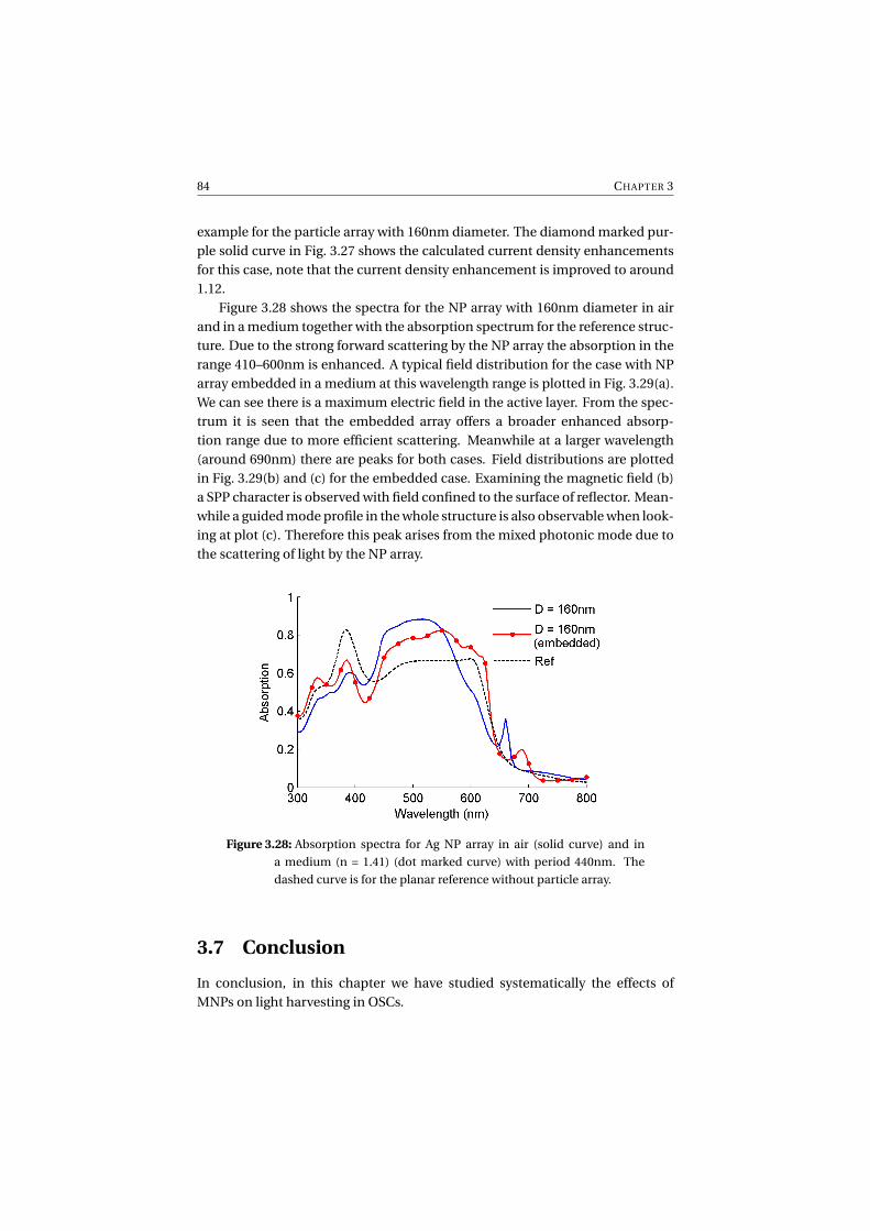
84 CHAPTER 3
example for the particle array with 160nm diameter. The diamond marked pur-ple solid curve in Fig. 3.27 shows the calculated current density enhancementsfor this case, note that the current density enhancement is improved to around1.12.
Figure 3.28 shows the spectra for the NP array with 160nm diameter in airand in a medium together with the absorption spectrum for the reference struc-ture. Due to the strong forward scattering by the NP array the absorption in therange 410–600nm is enhanced. A typical field distribution for the case with NParray embedded in a medium at this wavelength range is plotted in Fig. 3.29(a).We can see there is a maximum electric field in the active layer. From the spec-trum it is seen that the embedded array offers a broader enhanced absorp-tion range due to more efficient scattering. Meanwhile at a larger wavelength(around 690nm) there are peaks for both cases. Field distributions are plottedin Fig. 3.29(b) and (c) for the embedded case. Examining the magnetic field (b)a SPP character is observed with field confined to the surface of reflector. Mean-while a guided mode profile in the whole structure is also observable when look-ing at plot (c). Therefore this peak arises from the mixed photonic mode due tothe scattering of light by the NP array.
Figure 3.28: Absorption spectra for Ag NP array in air (solid curve) and in
a medium (n = 1.41) (dot marked curve) with period 440nm. The
dashed curve is for the planar reference without particle array.
3.7 Conclusion
In conclusion, in this chapter we have studied systematically the effects ofMNPs on light harvesting in OSCs.
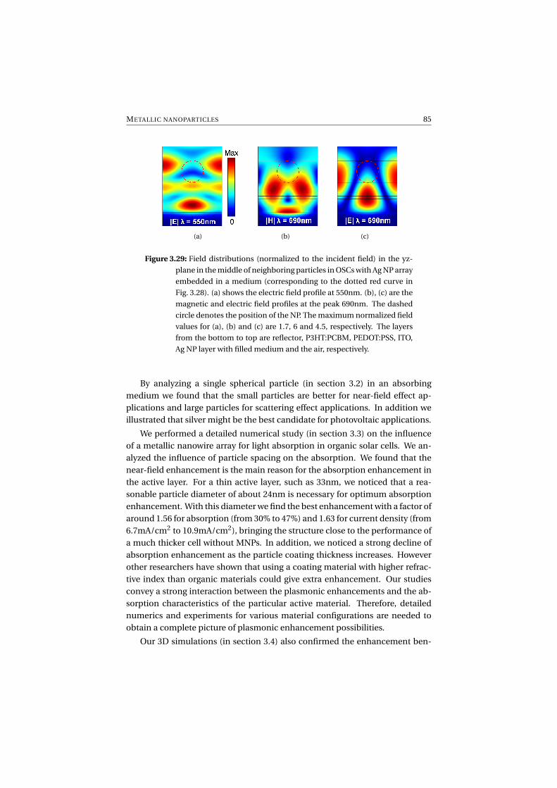
METALLIC NANOPARTICLES 85
(a) (b) (c)
Figure 3.29: Field distributions (normalized to the incident field) in the yz-
plane in the middle of neighboring particles in OSCs with Ag NP array
embedded in a medium (corresponding to the dotted red curve in
Fig. 3.28). (a) shows the electric field profile at 550nm. (b), (c) are the
magnetic and electric field profiles at the peak 690nm. The dashed
circle denotes the position of the NP. The maximum normalized field
values for (a), (b) and (c) are 1.7, 6 and 4.5, respectively. The layers
from the bottom to top are reflector, P3HT:PCBM, PEDOT:PSS, ITO,
Ag NP layer with filled medium and the air, respectively.
By analyzing a single spherical particle (in section 3.2) in an absorbingmedium we found that the small particles are better for near-field effect ap-plications and large particles for scattering effect applications. In addition weillustrated that silver might be the best candidate for photovoltaic applications.
We performed a detailed numerical study (in section 3.3) on the influenceof a metallic nanowire array for light absorption in organic solar cells. We an-alyzed the influence of particle spacing on the absorption. We found that thenear-field enhancement is the main reason for the absorption enhancement inthe active layer. For a thin active layer, such as 33nm, we noticed that a rea-sonable particle diameter of about 24nm is necessary for optimum absorptionenhancement. With this diameter we find the best enhancement with a factor ofaround 1.56 for absorption (from 30% to 47%) and 1.63 for current density (from6.7mA/cm2 to 10.9mA/cm2), bringing the structure close to the performance ofa much thicker cell without MNPs. In addition, we noticed a strong decline ofabsorption enhancement as the particle coating thickness increases. Howeverother researchers have shown that using a coating material with higher refrac-tive index than organic materials could give extra enhancement. Our studiesconvey a strong interaction between the plasmonic enhancements and the ab-sorption characteristics of the particular active material. Therefore, detailednumerics and experiments for various material configurations are needed toobtain a complete picture of plasmonic enhancement possibilities.
Our 3D simulations (in section 3.4) also confirmed the enhancement ben-

86 CHAPTER 3
efits from the near-field effects of MNPs embedded in active layer in a moreconcrete OSC structure. We demonstrated that the current density is improvedfrom 7.3mA/cm2 to 10.7mA/cm2 with an enhancement factor of ∼ 1.46. Simu-lations with Au particles embedded in the buffer layer imply that the observedefficiency improvement in reported experiments with particles (both Ag and Au)in the buffer layer may be due to improved electrical effects like decreased resis-tance, improved exciton dissociation or carrier collection. The experiments (insection 3.5) carried out by colleagues at imec together with our simulations haveconfirmed that near-field enhancement of particles can boost the light harvest-ing.
Finally we also demonstrated the feasibility of the enhanced scattering ofMNPs in boosting the efficiency of OSCs. By using arrays with larger NPs thelight can be scattered into the active layer, improving the light harvesting. Fur-ther improvement can be achieved by filling the space between particles in theNP array with a medium.
METALLIC NANOPARTICLES 87
References
[1] H. Hoppe and N. S. Sariciftci. Organic solar cells: an overview. Journal ofMaterials Research, 19(7):1924–1945, 2004.
[2] W. W. Kromhout. UCLA engineers create tandem polymer solar cells that setrecord for energy-conversion. Technical report, University of California, LosAngeles, February 2012.
[3] G. Yu, J. Gao, J. C. Hummelen, F. Wudl, and A. J. Heeger. Polymer photo-voltaic cells: enhanced efficiencies via a network of internal donor-acceptorheterojunctions. Science, 270(5243):1789–1791, 1995.
[4] T. Soga. Nanostructured Materials for Solar Energy Conversion. ElsevierScience, 2006.
[5] V. Andersson, K. Tvingstedt, and O. Inganäs. Optical modeling of a foldedorganic solar cell. Journal of Applied Physics, 103(9):094520, 2008.
[6] B. P. Rand, S. R. Forrest, and P. Peumans. Long-range absorption enhance-ment in organic tandem thin-film solar cells containing silver nanoclusters.Journal of Applied Physics, 96(9):7519, 2004.
[7] J.Y. Kim, K. Lee, N.E. Coates, D. Moses, T.Q. Nguyen, M. Dante, and A.J.Heeger. Efficient tandem polymer solar cells fabricated by all-solution pro-cessing. Science, 317(5835):222–225, 2007.
[8] J. Yang, J. You, C.-C. Chen, W.-C. Hsu, H.-R. Tan, X. W. Zhang, Z. Hong, andY. Yang. Plasmonic polymer tandem solar cell. ACS Nano, 5(8):6210–7, 2011.
[9] S. R. Forrest. The limits to organic photovoltaic cell efficiency. MRS Bulletin,30(01):28–32, 2005.
[10] W.Y. Wong, X. Z. Wang, Z. He, B. D. Aleksandra, C. T. Yip, K. Y. Cheung,H. Wang, C. S. K. Mak, and W. K. Chan. Metallated conjugated polymers asa new avenue towards high-efficiency polymer solar cells. Nature Materials,6(7):521–527, 2007.
[11] M. Westphalen, U. Kreibig, J. Rostalski, H. Lüth, and D. Meissner. Metalcluster enhanced organic solar cells. Solar Energy Materials and Solar Cells,61(1):97–105, 2000.
[12] J. W. Wang, X.and Ho, Q. Yang, H. L. Tam, G. X. Li, K.W. Cheah, and F. Zhu.Performance enhancement in organic photovoltaic devices using plasma-polymerized fluorocarbon-modified Ag nanoparticles. Organic Electronics,12(11):1943–1947, 2011.

88 CHAPTER 3
[13] A.J. Morfa, K. L. Rowlen, T. H. Reilly III, M. J. Romero, and J. V. D. Lagemaat.Plasmon-enhanced solar energy conversion in organic bulk heterojunctionphotovoltaics. Applied Physics Letters, 92:013504, 2008.
[14] S. S. Kim, S. I. Na, J. Jo, D. Y. Kim, and Y. C. Nah. Plasmon enhanced per-formance of organic solar cells using electrodeposited Ag nanoparticles. Ap-plied Physics Letters, 93(7):073307, 2008.
[15] D. Duche, P. Torchio, L. Escoubas, F. Monestier, J. J. Simon, F. Flory, andG. Mathian. Improving light absorption in organic solar cells by plasmoniccontribution. Solar Energy Materials and Solar Cells, 93(8):1377–1382,2009.
[16] X. Chen, C. Zhao, L. Rothberg, and M. K. Ng. Plasmon enhancement ofbulk heterojunction organic photovoltaic devices by electrode modification.Applied Physics Letters, 93(12):123302, 2008.
[17] D. Qu, F. Liu, Y. Huang, W. Xie, and Q. Xu. Mechanism of optical absorp-tion enhancement in thin film organic solar cells with plasmonic metalnanoparticles. Optics Express, 19(24):24795–803, 2011.
[18] K. Kim and D. L. Carroll. Roles of Au and Ag nanoparticles in efficiencyenhancement of poly(3-octylthiophene)/C[sub 60] bulk heterojunction pho-tovoltaic devices. Applied Physics Letters, 87(20):203113, 2005.
[19] D. H. Wang, K. H. Park, J. H. Seo, J. Seifter, J. H. Jeon, J. K. Kim, J. H.Park, O. O. Park, and A. J. Heeger. Enhanced power conversion efficiencyin PCDTBT/PC70BM bulk heterojunction photovoltaic devices with embed-ded silver nanoparticle clusters. Advanced Energy Materials, 1(5):766–70,2011.
[20] D. H. Wang, D. Y. Kim, K. W. Choi, J. H. Seo, S. H. Im, J. H. Park, O. O. Park,and A. J. Heeger. Enhancement of donor-acceptor polymer bulk heterojunc-tion solar cell power conversion efficiencies by addition of Au nanoparticles.Angewandte Chemie International Edition, 50(24):5519–523, 2011.
[21] H. Shen, P. Bienstman, and B. Maes. Plasmonic absorption enhancementin organic solar cells with thin active layers. Journal of Applied Physics,106(7):073109–073109, 2009.
[22] L. Hu, X. Chen, and G. Chen. Surface-plasmon enhanced near-bandgaplight absorption in silicon photovoltaics. Journal of Computational andTheoretical Nanoscience, 5(11):2096–2101, 2008.

METALLIC NANOPARTICLES 89
[23] Y. A. Akimov, W. S. Koh, and K. Ostrikov. Enhancement of optical absorptionin thin-film solar cells through the excitation of higher-order nanoparticleplasmon modes. Optics Express, 17(12):10195–205, 2009.
[24] A. Paris, A. Vaccari, A. Calà Lesina, E. Serra, and L. Calliari. Plasmonic scat-tering by metal nanoparticles for solar cells. Plasmonics, 2012.
[25] D. Derkacs, S. H. Lim, P. Matheu, W. Mar, and E. T. Yu. Improved per-formance of amorphous silicon solar cells via scattering from surface plas-mon polaritons in nearby metallic nanoparticles. Applied Physics Letters,89(9):093103, 2006.
[26] S. Pillai, K. R. Catchpole, T. Trupke, and M. A. Green. Surface plasmon en-hanced silicon solar cells. Journal of Applied Physics, 101(9):093105, 2007.
[27] S. H. Lim, W. Mar, P. Matheu, D. Derkacs, and E. T. Yu. Photocurrent spec-troscopy of optical absorption enhancement in silicon photodiodes via scat-tering from surface plasmon polaritons in gold nanoparticles. Journal ofApplied Physics, 101(10):104309, 2007.
[28] K. R. Catchpole and A. Polman. Design principles for particle plasmon en-hanced solar cells. Applied Physics Letters, 93(19):191113, 2008.
[29] S. Mokkapati, F. J. Beck, A. Polman, and K. R. Catchpole. Designing periodicarrays of metal nanoparticles for light-trapping applications in solar cells.Applied Physics Letters, 95(5):053115, 2009.
[30] Y. A. Akimov and W. S. Koh. Resonant and nonresonant plasmonicnanoparticle enhancement for thin-film silicon solar cells. Nanotechnol-ogy, 21(23):235201, 2010.
[31] Y. A. Akimov and K Ostrikov E P Li. Surface plasmon enhancement of opticalabsorption in thin-film silicon solar cells. Physics Reports Review SectionOf Physics Letters, pages 107–113, 2009.
[32] F.-J. Tsai, J.-Y. Wang, J.-J. Huang, Y.-W. Kiang, and C. C. Yang. Absorp-tion enhancement of an amorphous Si solar cell through surface plasmon-induced scattering with metal nanoparticles. Optics Express, 18(102):A207–20, 2010.
[33] Y. A. Akimov and W. S. Koh. Tolerance study of nanoparticle enhancementfor thin-film silicon solar cells. Applied Physics Letters, 99(6):063102, 2011.
[34] Y. A. Akimov and W. S. Koh. Design of Plasmonic Nanoparticles for Effi-cient Subwavelength Light Trapping in Thin-Film Solar Cells. Plasmonics,6(1):155–161, 2010.
90 CHAPTER 3
[35] Y. C. Chang, F. Y. Chou, P. H. Yeh, H. W. Chen, S.-H. Chang, Y. C. Lan, T. F.Guo, T. C. Tsai, and C. T. Lee. Effects of surface plasmon resonant scatteringon the power conversion efficiency of organic thin-film solar cells. Journal ofVacuum Science & Technology B: Microelectronics and Nanometer Struc-tures, 25(6):1899, 2007.
[36] S. Mokkapati, F. J. Beck, R. de Waele, A. Polman, and K. R. Catchpole. Res-onant nano-antennas for light trapping in plasmonic solar cells. Journal ofPhysics D: Applied Physics, 44(18):185101, 2011.
[37] A. Pors, A. V. Uskov, M. Willatzen, and I. E. Protsenko. Control of the inputefficiency of photons into solar cells with plasmonic nanoparticles. OpticsCommunications, 284(8):2226–2229, 2011.
[38] W. Ren, G. Zhang, Y. Wu, H. Ding, Q. Shen, and K. Zhang. Broadband ab-sorption enhancement achieved by optical layer mediated plasmonic solarcell. Optics Express, 19(27):26536–26550, 2011.
[39] F. Moreno, J. M. Saiz, and F. González. Interaction of nanoparticles withsubstrates : effects on the dipolar behaviour of the particles. Optics Express,16(17):2034–2038, 2008.
[40] E. D. Palik. Handbook of Optical Constants of Solids. Academic, New York,1985.
[41] H. Wang, F. Tam, N. K. Grady, and N. J. Halas. Cu nanoshells: effects ofinterband transitions on the nanoparticle plasmon resonance. The Journalof Physical Chemistry. B, 109(39):18218–22, 2005.
[42] B. Zimmermann, M. Glatthaar, M. Niggemann, M. Riede, A. Hinsch, andA. Gombert. ITO-free wrap through organic solar cells– A module conceptfor cost-efficient reel-to-reel production. Solar Energy Materials and SolarCells, 91(5):374–378, 2007.
[43] F. Monestier, J. Simon, P. Torchio, L. Escoubas, F. Flory, S. Bailly, R. Debet-tignies, S. Guillerez, and C. Defranoux. Modeling the short-circuit currentdensity of polymer solar cells based on P3HT:PCBM blend. Solar Energy Ma-terials and Solar Cells, 91(5):405–410, 2007.
[44] L. Novotny and B. Hecht. Handbook of Optical Constants of Solids. Cam-bridge University Press, Cambridge, 2006.
[45] C. Rockstuhl, S. Fahr, and F. Lederer. Absorption enhancement in so-lar cells by localized plasmon polaritons. Journal of Applied Physics,104(12):123102, 2008.

METALLIC NANOPARTICLES 91
[46] S.H. Park, A. Roy, S. Beaupré, S. Cho, N. Coates, J.S. Moon, D. Moses,M. Leclerc, K. Lee, and A.J. Heeger. Bulk heterojunction solar cells with in-ternal quantum efficiency approaching 100%. Nature Photonics, 3(5):297–302, 2009.
[47] J. Y. Lee and P. Peumans. The origin of enhanced optical absorption in solarcells with metal nanoparticles embedded in the active layer. Optics Express,18(10):10078–87, 2010.
[48] M. A. Sefunc, A. K. Okyay, and H. V. Demir. Volumetric plasmonic resonatorarchitecture for thin-film solar cells. Applied Physics Letters, 98(9):093117,2011.
[49] M. G. Kang, T. Xu, H. J. Park, X. Luo, and L. J. Guo. Efficiency enhancementof organic solar cells using transparent plasmonic Ag nanowire electrodes.Advanced Materials, 22(39):4378–83, 2010.
[50] H. Shen and B. Maes. Combined plasmonic gratings in organic solar cells.Optics Express, 19(106):A1202–A1210, 2011.
[51] F. C. Chen, J. L. Wu, C. L. Lee, Y. Hong, C. H. Kuo, and M. H. Huang.Plasmonic-enhanced polymer photovoltaic devices incorporating solution-processable metal nanoparticles. Applied Physics Letters, 95(1):013305,2009.
[52] J. H. Lee, J. H. Park, J. S. Kim, D. Y. Lee, and K. Cho. High efficiency polymersolar cells with wet deposited plasmonic gold nanodots. Organic Electron-ics, 10(3):416–420, 2009.
[53] J. L. Wu, F. C. Chen, Y. S. Hsiao, F. C. Chien, P. Chen, C. H. Kuo, M. H.Huang, and C. S. Hsu. Surface plasmonic effects of metallic nanoparticleson the performance of polymer bulk heterojunction solar cells. ACS Nano,5(2):959–67, 2011.
[54] B. Niesen, B.P. Rand, P. Van Dorpe, H. Shen, B. Maes, J. Genoe, and P. Here-mans. Excitation of multiple dipole surface plasmon resonances in spheri-cal silver nanoparticles. Optics Express, 18(18):19032–19038, 2010.

4Metallic gratings
4.1 Introduction
Metallic nanoparticles can provide a decent light harvesting boost by blend-ing them in the active layer, as discussed in the previous chapter. Howeverthey suffer experimentally from random distribution and clustering which maydecrease the effects of plasmonic modes. As the advances in nanostructurefabrication technologies are developed, another prominent possibility for plas-monic structures are metallic gratings, including nano-structured metallic sur-faces and periodic island gratings (both 1D and 2D). The experimental advan-tage of these types of metallic gratings over nanoparticles is the precise spatialcontrol. The benefits of these gratings for light trapping are due to the strongand localized electromagnetic fields, which is a consequence of the excitationof plasmon polaritons, as we discuss in this chapter.
Various novel structures have been proposed to enhance light harvestingby using periodic metallic gratings in both organic [1–9] and inorganic solarcells [10–17]. In these structures plasmonic mode excitations are divided intolocalized modes, such as in nanoparticles (Localized Surface Plasmons, LSPs),and propagating modes at interfaces (Surface Plasmon Polaritons, SPPs). Instructures with a layer of periodic metallic islands and a nearby metallic sur-face, mixtures of LSPs and SPPs can be excited depending on the period. Forsmall periods (< 300nm), LSPs are mainly the reason for the light harvesting
94 CHAPTER 4
improvement [2–5]. Scattering into SPPs comes into effect for larger grating pe-riods [1, 6, 9, 10, 15]. In addition, the angular dependent dispersion behavior ofthese plasmonic modes is complex [18–22] due to the plasmonic bandgap intro-duced by the periodic corrugation. For example, two different kinds of modesare observed, the so-called bright and dark modes, with symmetric and anti-symmetric field distributions respectively [22, 23]. They have been observed nu-merically [1] and experimentally [21, 24, 25] in some periodic plasmonic nanos-tructures. Dark modes are not excitable at the standard perpendicular inci-dence and need an oblique angle (or an asymmetric structure), so that opti-mized light trapping becomes more intricate.
In this chapter we mainly focus on metallic gratings to boost light harvest-ing in organic solar cells. In sections 4.2 to 4.4 we examine the combination ofmultiple gratings (1D), both on the front and back surface of the absorbing layer(model in Fig 4.1(a)). Most previous works focus on how a single nanophotonicfeature can enhance the absorption. The study of combined elements to worktowards the ultimate light-trapping configuration is less explored [4, 26, 27]. In-deed, it is an open question which combined structures will provide superposedresonances for maximum absorption enhancement.
Remark that our type of offset gratings can naturally form in fabrication pro-cesses with conformal layers, as was observed for example in [2]. Thus, here wecomplement these types of experiments with detailed numerical calculations.We start from structures with bare front and back gratings and end up with com-bined gratings. We discuss the modal origin of the enhanced absorption in theactive layer. Moreover, to better understand the modes we examine the angle-dependent behavior, which is also important for solar cells in practice. Finally insection 4.5 we provide a preliminary investigation on Ag disk arrays localized ina buffer layer of organic solar cells, which is a 2D version of the 1D front grating.
4.2 Geometry and methodology
4.2.1 Structures and simulation techniques
As the model in Fig 4.1(a) illustrates we propose an OSC structure with front andback silver gratings. The gratings are characterized by the width and height w f g ,h f g for front grating, wbg , hbg for back grating, and the period p. Throughoutour investigations the thickness of the active layer is chosen to be 50nm, cor-responding to the first Fabry-Perot maximum for the integrated absorption ina planar reference structure without gratings. Note that we include a half pe-riod offset between the two gratings, so that they operate quasi-independently.If the elements are on top of each other, thus without offset [4], this leads todifferent resonances than the individual cases, and can in general give stronger
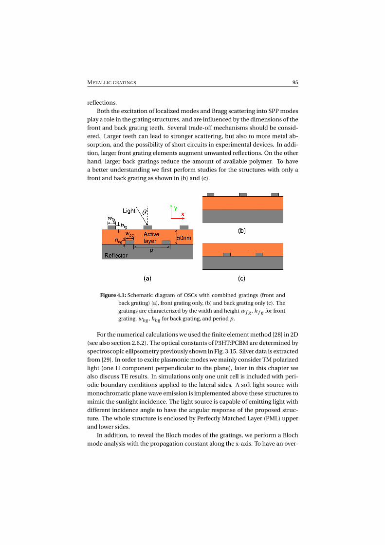
METALLIC GRATINGS 95
reflections.Both the excitation of localized modes and Bragg scattering into SPP modes
play a role in the grating structures, and are influenced by the dimensions of thefront and back grating teeth. Several trade-off mechanisms should be consid-ered. Larger teeth can lead to stronger scattering, but also to more metal ab-sorption, and the possibility of short circuits in experimental devices. In addi-tion, larger front grating elements augment unwanted reflections. On the otherhand, larger back gratings reduce the amount of available polymer. To havea better understanding we first perform studies for the structures with only afront and back grating as shown in (b) and (c).
Figure 4.1: Schematic diagram of OSCs with combined gratings (front and
back grating) (a), front grating only, (b) and back grating only (c). The
gratings are characterized by the width and height w f g , h f g for front
grating, wbg , hbg for back grating, and period p.
For the numerical calculations we used the finite element method [28] in 2D(see also section 2.6.2). The optical constants of P3HT:PCBM are determined byspectroscopic ellipsometry previously shown in Fig. 3.15. Silver data is extractedfrom [29]. In order to excite plasmonic modes we mainly consider TM polarizedlight (one H component perpendicular to the plane), later in this chapter wealso discuss TE results. In simulations only one unit cell is included with peri-odic boundary conditions applied to the lateral sides. A soft light source withmonochromatic plane wave emission is implemented above these structures tomimic the sunlight incidence. The light source is capable of emitting light withdifferent incidence angle to have the angular response of the proposed struc-ture. The whole structure is enclosed by Perfectly Matched Layer (PML) upperand lower sides.
In addition, to reveal the Bloch modes of the gratings, we perform a Blochmode analysis with the propagation constant along the x-axis. To have an over-

96 CHAPTER 4
all figure of merit, we calculate the total absorption ηtotA , which integrates the
absorption spectrum over the wavelength range from 300 to 800nm weightedby the AM 1.5G solar spectrum as defined in Eq. 3.3. Finally, we also provideexpected current densities (see Eq. 3.4) for these structures.
4.2.2 Bright and dark modes
We first consider an easier reference structure, with only a flat silver substratefollowed by a layer of P3HT:PCBM with 50nm thickness, forming a metal-dielectric-air (MDA) surface. The exact value of the SPP wave vector (kspp ) inthis structure can be calculated numerically by solving a transcendental equa-tion [30]
e2γ2d =(ε1γ2 − ε2γ1
)(ε3γ2 − ε2γ3
)(ε1γ2 + ε2γ1
)(ε1γ2 + ε2γ1
) (4.1)
where γi =√
k2spp −k2
0εi , i = 1, 2, and 3, and εi (i = 1, 2, 3) represent the permit-tivities of Ag, P3HT:PCBM and air, respectively. k0 is the wave vector of light inair. It is known that there is a mismatch between the SPP wave vector and thein-plane wave vector (parallel to the silver substrate component) of light in air.As a result it is impossible to excite SPPs directly (see also section 2.3). Here byintroducing gratings this mismatch can be overcome.
Due the scattering and the periodicity of the grating as discussed in chapter2, light shining on the OSCs with gratings (front or back gratings) can be cou-pled to the SPP mode in the multilayered structure when satisfying the Braggcondition
kspp = k0 sinθ ± NG = kx ± NG (4.2)
where kx is the in-plane light wave vector, θ is the light incidence angle withrespect to the normal, N is any integer, G = 2π/p, and p is the grating period.
The SPP mode will be tuned if a periodic grating is introduced. Howeverfor shallow periodic perturbations, the SPP wave vector is still approximatelyaccording to Eq. 4.1. Here the OSCs with front, back or combined grating con-tain relatively large variations, so Eq. 4.1 is no longer valid. Therefore, to get thecorrect dispersion Bloch mode calculations are necessary.
As shortly described in chapter 2, a periodic perturbation will introducea SPP bandgap due to the separation of the mode into two different modes,namely a bright and a dark mode. Here we look into these possible Bloch modesin the grating structures, calculated via the eigen-frequency solver implementedin COMSOL [28]. Figure 4.2 shows the calculated electric field distributions forbright and dark modes for gratings with period 490nm. Surface charge (sign ‘⊕’and ‘ª’ denote positive and negative charges respectively) distributions at themetallic reflector are also sketched, derived from the electric field distribution.The left column (a), (c) and (e) correspond to the bright modes of front, back

METALLIC GRATINGS 97
(a) (b)
(c) (d)
(e) (f)
Figure 4.2: Schematics of electric field (red arrows) and surface charges (signs
‘⊕’ and ‘ª’ denote positive and negative charges respectively) distri-
bution for bright and dark modes. The left column (a), (c) and (e)
correspond to the bright modes of front, back and combined grat-
ing respectively. The right column (b), (d) and (f) are the dark modes.
Only the surface charges at metal reflector are considered. Due to the
symmetry and charge conservation at the metal reflector the left col-
umn only yields non-zero net dipole along x-axis (parallel to reflec-
tor interface), while the right column yields non-zero net dipole along
y-axis (perpendicular to reflector interface). In these figures, front
gratings have a size of w f g = 60nm, h f g = 10nm, back grating with
wbg = 60nm, hbg = 30nm, and period 490nm.

98 CHAPTER 4
and combined grating respectively. The right column (b), (d) and (f) are the darkmodes. Due to the symmetry and charge conservation at the metallic reflectorthe left column yields a non-zero net dipole moment along the x-axis, while theright column has a non-zero net dipole moment along the y-axis. Therefore, forTM incident light the net dipole of a bright mode can always couple with theincident light, since it has an overlap with the incident electric field. In contrast,for the dark mode with net dipole along the y-axis, it can only be excited withtilted light.
Figure 4.2 also indicates that for a constant period the size of the gratingswill influence the resonance positions of SPP Bloch modes. Indeed, these ge-ometrical parameters will influence the distance between the surface charges,which consequently changes the response of surface charges to the incominglight. As examples figure 4.3 shows the size dependence of the bright and darkmodes in bare front and back gratings. For instance increasing the width of thefront grating will separate the negative and positive charges further away lead-ing to a red-shift of the bright mode. Increasing the height will bring the surfacecharges closer effectively resulting in a blue-shift of the bright mode, becauseof increased coupling between the front grating and metallic reflector. Whereasfor the back grating increasing the width will decrease the effective distance be-tween charges due to the more gentle deformation of the surface of metallicreflector; this results in a blue-shift of the bright mode. Increasing the heightwill induce a red-shift of the bright mode because of increased deformation ofthe surface.
A similar analysis can be done for the dark modes. However, note that theabove analysis is not rigorous especially for the back grating. Since the defor-mation of the surface of the reflector will dramatically change the properties ofBloch modes. For example with a large width of back grating the geometry be-comes grooves instead of ridges (the case considered here), and the propertiesof the Bloch modes in these two cases are very different 1.Therefore from theseconsiderations the grating sizes have to be chosen carefully, in order to makethe SPP Bloch mode contribute to the light harvesting.
4.3 Optimization for OSCs with a single grating
For the combined gratings there are five parameters to optimize, width andheight of front and back gratings, w f g and h f g , wbg and hbg respectively andperiod p. To simplify the problem and reveal the influence of bare front or backgrating on the performance it is necessary to investigate the OSCs with a single
1Further investigation shows that the frequency of the bright mode is larger than that of the darkmode for ridges, while for grooves it is the other way around. Meanwhile the corresponding sizedependence is also different.
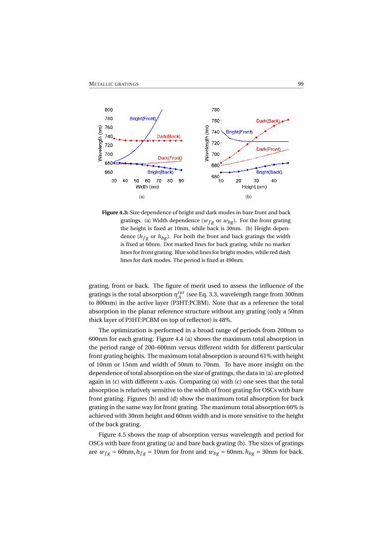
METALLIC GRATINGS 99
(a) (b)
Figure 4.3: Size dependence of bright and dark modes in bare front and back
gratings. (a) Width dependence (w f g or wbg ). For the front grating
the height is fixed at 10nm, while back is 30nm. (b) Height depen-
dence (h f g or hbg ). For both the front and back gratings the width
is fixed at 60nm. Dot marked lines for back grating, while no marker
lines for front grating. Blue solid lines for bright modes, while red dash
lines for dark modes. The period is fixed at 490nm.
grating, front or back. The figure of merit used to assess the influence of thegratings is the total absorption ηtot
A (see Eq. 3.3, wavelength range from 300nmto 800nm) in the active layer (P3HT:PCBM). Note that as a reference the totalabsorption in the planar reference structure without any grating (only a 50nmthick layer of P3HT:PCBM on top of reflector) is 48%.
The optimization is performed in a broad range of periods from 200nm to600nm for each grating. Figure 4.4 (a) shows the maximum total absorption inthe period range of 200–600nm versus different width for different particularfront grating heights. The maximum total absorption is around 61% with heightof 10nm or 15nm and width of 50nm to 70nm. To have more insight on thedependence of total absorption on the size of gratings, the data in (a) are plottedagain in (c) with different x-axis. Comparing (a) with (c) one sees that the totalabsorption is relatively sensitive to the width of front grating for OSCs with barefront grating. Figures (b) and (d) show the maximum total absorption for backgrating in the same way for front grating. The maximum total absorption 60% isachieved with 30nm height and 60nm width and is more sensitive to the heightof the back grating.
Figure 4.5 shows the map of absorption versus wavelength and period forOSCs with bare front grating (a) and bare back grating (b). The sizes of gratingsare w f g = 60nm,h f g = 10nm for front and wbg = 60nm,hbg = 30nm for back.

100 CHAPTER 4
Figure 4.4: Maximum total absorption in the period range of 200nm–600nm
in active layer versus width of front (a) and back (b) grating in OSCs
with a single grating. Data on (c) and (d) are the same as (a) and (b)
respectively but presented in different ways to have an impression of
the sensitivity of absorption on width and height of grating.
Notice that peaks show up for period larger than 350nm at 700–800nm wave-length range in (a) for bare grating. These peaks correspond to the surface plas-mon at the reflector/active layer interface (will be verified in Fig. 4.6), which arecoupled from incident light by the scattering of the front grating. While the sur-face plasmon peaks for the bare back grating tend to excite at low wavelengthsnear 600nm with relatively weak intensity. This may be due to the ridge of theback grating not being a good scatterer [31].
Figure 4.6 (a) shows the absorption spectra for OSCs with bare front andback grating together with that of the planar reference structure. Note that thefront grating tends to enhance absorption at large wavelengths, while the backgrating enhances at small wavelengths (range 330–700nm). To get more insightthe corresponding field distributions of the peaks (at 740nm and 670nm forfront and back grating respectively) are shown in (b)–(e). A mixture betweenlocalized (LSP) and propagating (SPP) character is observed [21]. From the Hmagnitude we indeed see a strong coupling between the front grating elementand the back silver interface (see Fig. 4.6 (b)). From the E magnitude on the
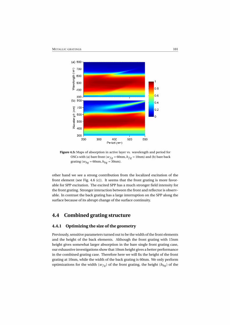
METALLIC GRATINGS 101
Figure 4.5: Maps of absorption in active layer vs. wavelength and period for
OSCs with (a) bare front (w f g = 60nm,h f g = 10nm) and (b) bare back
grating (wbg = 60nm,hbg = 30nm).
other hand we see a strong contribution from the localized excitation of thefront element (see Fig. 4.6 (c)). It seems that the front grating is more favor-able for SPP excitation. The excited SPP has a much stronger field intensity forthe front grating. Stronger interaction between the front and reflector is observ-able. In contrast the back grating has a large interruption on the SPP along thesurface because of its abrupt change of the surface continuity.
4.4 Combined grating structure
4.4.1 Optimizing the size of the geometry
Previously, sensitive parameters turned out to be the width of the front elementsand the height of the back elements. Although the front grating with 15nmheight gives somewhat larger absorption in the bare single front grating case,our exhaustive investigations show that 10nm height gives a better performancein the combined grating case. Therefore here we will fix the height of the frontgrating at 10nm, while the width of the back grating is 60nm. We only performoptimizations for the width (w f g ) of the front grating, the height (hbg ) of the
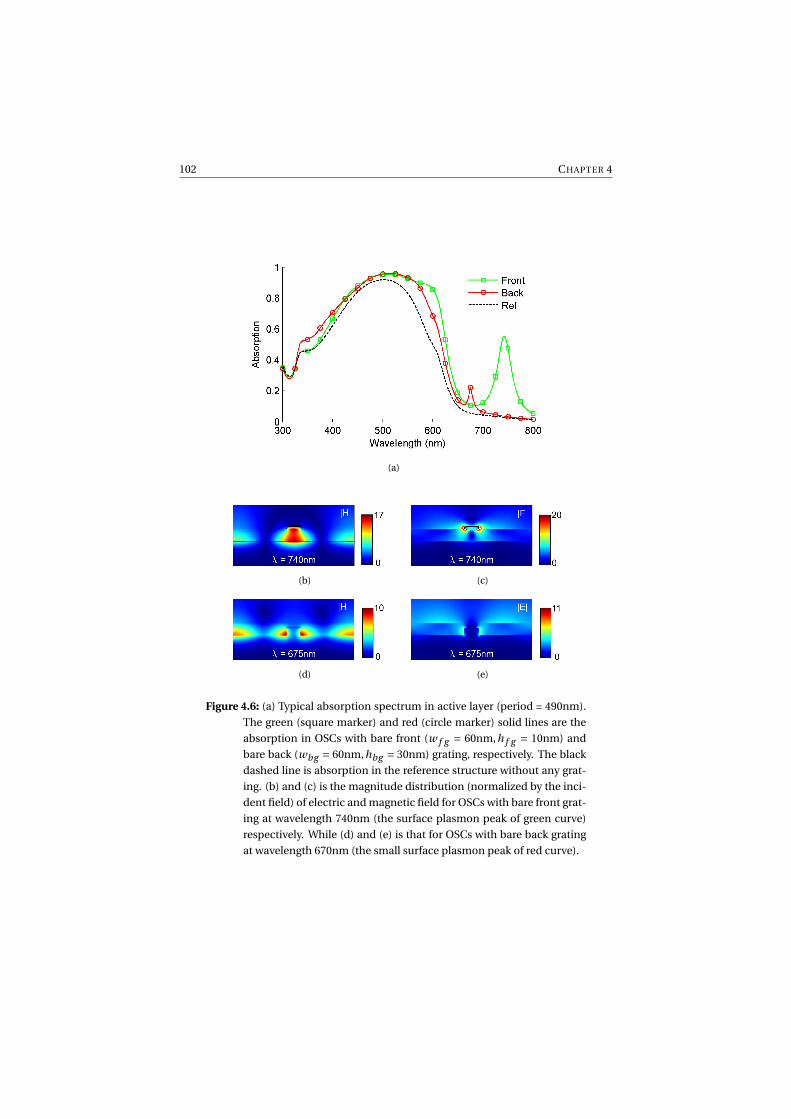
102 CHAPTER 4
(a)
(b) (c)
(d) (e)
Figure 4.6: (a) Typical absorption spectrum in active layer (period = 490nm).
The green (square marker) and red (circle marker) solid lines are the
absorption in OSCs with bare front (w f g = 60nm,h f g = 10nm) and
bare back (wbg = 60nm,hbg = 30nm) grating, respectively. The black
dashed line is absorption in the reference structure without any grat-
ing. (b) and (c) is the magnitude distribution (normalized by the inci-
dent field) of electric and magnetic field for OSCs with bare front grat-
ing at wavelength 740nm (the surface plasmon peak of green curve)
respectively. While (d) and (e) is that for OSCs with bare back grating
at wavelength 670nm (the small surface plasmon peak of red curve).

METALLIC GRATINGS 103
back grating and the period. Figure 4.7 shows the maximum total absorption(with optimized period) for different combinations of w f g and hbg . The overalloptimized total absorption is achieved with a width of 30nm for the back grat-ing, a width of 60nm for the front grating and the period 490nm. With theseparameters the total absorption is boosted from 48% (for reference structure)to 65%, thus an enhancement factor of 1.35. In the following sections we willfocus on these optimized grating sizes (w f g = 60nm, h f g = 10nm, wbg = 60nm,hbg = 30nm and period 490nm) to have more insight.
Figure 4.7: Maximum total absorption (with optimized period) in active ma-
terial versus the width of front grating and the height of the back grat-
ing. The height of front grating is fixed at 10nm whereas the width of
back grating is 60nm. The optimization is performed for the period
for each combination of width w f g of front grating and height hbg of
back grating.
4.4.2 Perpendicular incidence
We consider the optimized period of 490nm (value determined in the previoussubsection), and examine the absorption in the organic layer for perpendicularTM incidence, see Fig. 4.8(a). Here the spectrum is indicated for four structures:the planar reference structure without gratings, the front grating case with a flatback surface, the back grating case with a flat air-organic interface, and finallythe full combined grating case.
Examining the combined spectra in Fig. 4.8(a) provides insight in the partic-ular contributions. First, we notice the big peak around 740nm and the shoulderaround 600nm in both the front grating and the combined grating case. In con-trast, the shoulder of the combined case around 350nm fits well with the back

104 CHAPTER 4
(a)
(b)
(c) (d)
Figure 4.8: (a) The absorption spectra of the organic layer with combined
grating (blue solid line), front grating only (green dash-dotted), back
grating only (red dashed) and planar reference structure without grat-
ing (black dotted). (b) Intensity enhancement spectrum at a point
close to a lower corner of front grating (blue solid line) and at a point
close to an upper corner of back grating (red dashed line) for com-
bined grating, normalized by the incident field. (c) and (d) show the E
and H amplitude profile at wavelength 740nm for the combined case.

METALLIC GRATINGS 105
grating absorption. In addition, the small peak around 675nm of the back grat-ing case seems to help the combined case in that range. Thus, the back and thefront gratings make fairly independent contributions to different wavelengthranges and one arrives at a broadband enhancement from 350nm to 800nm inthe combined grating structure.
The broadband enhancement is attributed to the enhanced field intensityin the vicinity of gratings due to the excitation of LSPs and SPPs at differentwavelengths. To verify this, Fig. 4.8(b) shows the intensity enhancement in theorganic layer in the vicinity of the front and back teeth for combined gratingstructures. The intensity enhancement is the intensity ratio at a certain pointbetween the cell with a combined grating and the incident field. We notice thestrongly enhanced intensity at larger wavelengths (λ> 600nm), but the point oflargest ratio (near front or back grating) depends on the particular wavelengthrange.
To better understand the property of the main peak at 740nm, electric E andmagnetic H field magnitude distributions are shown Fig. 4.8(c) and (d). Heresimilar to the field distributions for bare front and back grating (Fig. 4.6 (b)–(e)) a mixture between localized (LSP) and propagating (SPP) character is stillobserved, in spite of a much stronger perturbation. Moreover the field distribu-tion looks like a superposition of SPP fields (although peaks are not at the samewavelength) in Fig. 4.6 (b)–(e), indicating that the coupling between the frontand back gratings is relatively small at this optimized period.
4.4.3 Period dependence
The period has a strong influence on the grating behavior. Therefore, we con-sider here the dependence on the period for the combined grating structure, seeFig. 4.9(a) for normal TM incidence.
For periods larger than 350nm there is an important absorption peak show-ing up at larger wavelengths (λ> 650nm), already discussed in the previous sec-tion. This plasmonic resonance red-shifts as the period increases, and finallyleaves the absorption tail of the organic material. The strong absorption in thewavelength range 400 to 650nm for periods between 300nm and 600nm is due tomore localized grating intensity enhancements, as they are quasi-independentof the period (but more dependent on the grating teeth size, not shown). As theperiod decreases below 300nm, the filling factor of the gratings gets large, lead-ing e.g. to strongly increased reflection. All of these factors together result in therelatively small absorption in the period range 200–300nm and the wavelengthrange 400–650nm.
These trends are reflected in Fig. 4.9(b) for the total absorption. At first morelight reaches the active layer, leading to a strong absorption increase. After the

106 CHAPTER 4
appearance of the large peak plasmonic mode a wide optimal plateau (withmaximum at 490nm) is reached, after which the mode shifts out of the absorp-tion tail and absorption decreases.
(a)
(b)
Figure 4.9: (a) Map of absorption in the organic layer versus the wavelength
of incident light and the grating period. (b) The period dependence of
total absorption (blue solid line). The value for the reference structure
is indicated by the black dotted line.
4.4.4 Angular dependence
For practical reasons it is important to explore the angular performance ofcells with plasmonic gratings. In addition, these studies give insight into theplasmonic modes, and even provide further opportunities for optimization.Fig. 4.10 maps the absorption in the active layer versus wavelength and lightincidence angle for the previously introduced structures: combined, front, backand planar case, respectively.
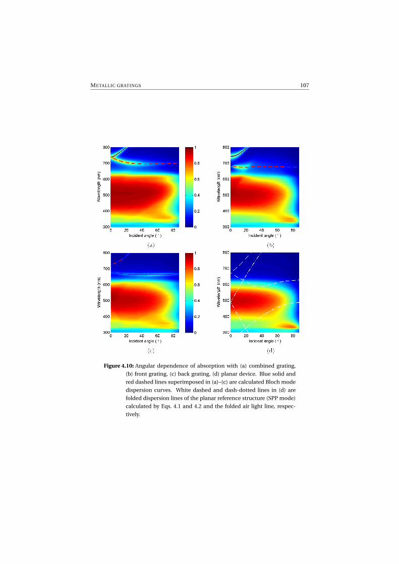
METALLIC GRATINGS 107
Figure 4.10: Angular dependence of absorption with (a) combined grating,
(b) front grating, (c) back grating, (d) planar device. Blue solid and
red dashed lines superimposed in (a)–(c) are calculated Bloch mode
dispersion curves. White dashed and dash-dotted lines in (d) are
folded dispersion lines of the planar reference structure (SPP mode)
calculated by Eqs. 4.1 and 4.2 and the folded air light line, respec-
tively.
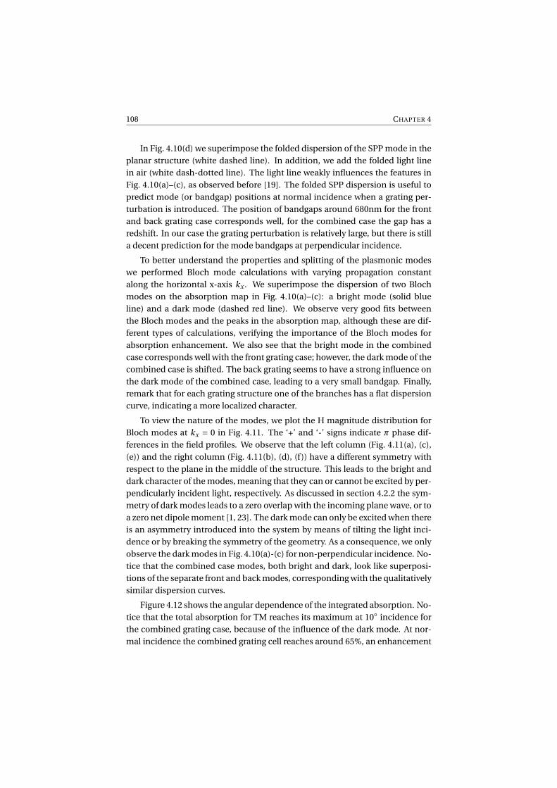
108 CHAPTER 4
In Fig. 4.10(d) we superimpose the folded dispersion of the SPP mode in theplanar structure (white dashed line). In addition, we add the folded light linein air (white dash-dotted line). The light line weakly influences the features inFig. 4.10(a)–(c), as observed before [19]. The folded SPP dispersion is useful topredict mode (or bandgap) positions at normal incidence when a grating per-turbation is introduced. The position of bandgaps around 680nm for the frontand back grating case corresponds well, for the combined case the gap has aredshift. In our case the grating perturbation is relatively large, but there is stilla decent prediction for the mode bandgaps at perpendicular incidence.
To better understand the properties and splitting of the plasmonic modeswe performed Bloch mode calculations with varying propagation constantalong the horizontal x-axis kx . We superimpose the dispersion of two Blochmodes on the absorption map in Fig. 4.10(a)–(c): a bright mode (solid blueline) and a dark mode (dashed red line). We observe very good fits betweenthe Bloch modes and the peaks in the absorption map, although these are dif-ferent types of calculations, verifying the importance of the Bloch modes forabsorption enhancement. We also see that the bright mode in the combinedcase corresponds well with the front grating case; however, the dark mode of thecombined case is shifted. The back grating seems to have a strong influence onthe dark mode of the combined case, leading to a very small bandgap. Finally,remark that for each grating structure one of the branches has a flat dispersioncurve, indicating a more localized character.
To view the nature of the modes, we plot the H magnitude distribution forBloch modes at kx = 0 in Fig. 4.11. The ‘+’ and ‘-’ signs indicate π phase dif-ferences in the field profiles. We observe that the left column (Fig. 4.11(a), (c),(e)) and the right column (Fig. 4.11(b), (d), (f)) have a different symmetry withrespect to the plane in the middle of the structure. This leads to the bright anddark character of the modes, meaning that they can or cannot be excited by per-pendicularly incident light, respectively. As discussed in section 4.2.2 the sym-metry of dark modes leads to a zero overlap with the incoming plane wave, or toa zero net dipole moment [1, 23]. The dark mode can only be excited when thereis an asymmetry introduced into the system by means of tilting the light inci-dence or by breaking the symmetry of the geometry. As a consequence, we onlyobserve the dark modes in Fig. 4.10(a)-(c) for non-perpendicular incidence. No-tice that the combined case modes, both bright and dark, look like superposi-tions of the separate front and back modes, corresponding with the qualitativelysimilar dispersion curves.
Figure 4.12 shows the angular dependence of the integrated absorption. No-tice that the total absorption for TM reaches its maximum at 10◦ incidence forthe combined grating case, because of the influence of the dark mode. At nor-mal incidence the combined grating cell reaches around 65%, an enhancement
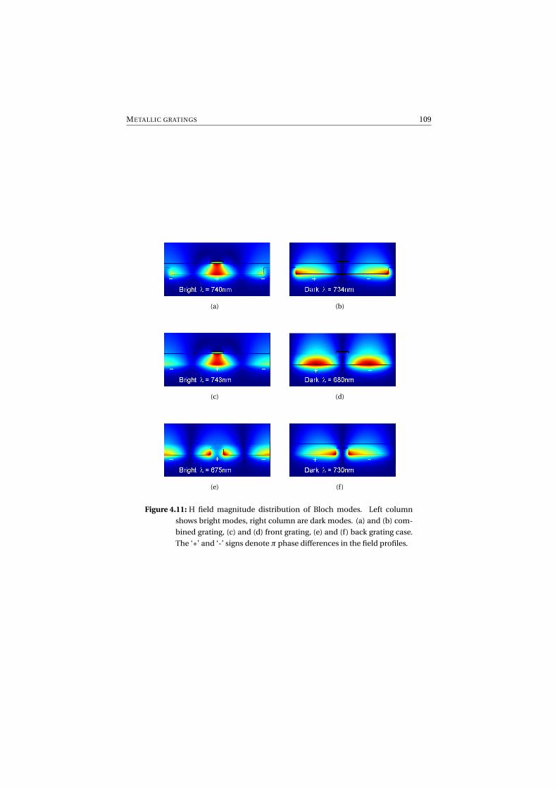
METALLIC GRATINGS 109
(a) (b)
(c) (d)
(e) (f)
Figure 4.11: H field magnitude distribution of Bloch modes. Left column
shows bright modes, right column are dark modes. (a) and (b) com-
bined grating, (c) and (d) front grating, (e) and (f) back grating case.
The ‘+’ and ‘-’ signs denote π phase differences in the field profiles.

110 CHAPTER 4
Figure 4.12: Total absorption versus incidence angle for TM (solid lines) and
TE (dashed) polarizations. Blue: combined grating; green: front grat-
ing; red: back grating. The dot marked lines (both dashed and solid)
for the planar structure.
factor of about 1.35 compared with the 48% of a planar cell, as discussed previ-ously. The dark mode effect at 10◦ leads to a further 67% absorption. Enhance-ment is quite angle insensitive and observed over a large angular range. Up toaround 70◦ the TM absorption is still larger than that of the reference at normalincidence. We can also see that the combined grating case dominates over thefront and back single grating cases. Although our structures were mainly opti-mized for perpendicular incidence, we remark that the dark modes provide animportant extra route towards enhancement.
As a final step we should consider the TE polarization performance, alsoshown in Fig. 4.12. For TE it is not possible to excite plasmonic modes, so in thiscase the silver grating works as absorber and scatterer. Only a very small en-hancement near perpendicular incidence for the front grating case is observed.A small decrease of absorption for the back and combined cases is seen for per-pendicular incidence, because the presence of the back grating reduces the ac-tive material. So for unpolarized perpendicular light, gratings can still enhancethe absorption with an average, relatively good enhancement factor of around1.2.
Another important parameter which assesses the overall electronic perfor-mance is the current density. Figure 4.13 shows the current density accord-ing to Eq. 3.4 with the assumption that the internal quantum efficiency is 1.Under TM-polarized normal incidence the reference has a current density of11.6mA/cm2, while the combined grating can enhance the current density to

METALLIC GRATINGS 111
16.5mA/cm2 with an enhancement factor of 1.42. The current density reachesits maximum 17.1mA/cm2 with a small incident tilt of around 10◦.
Figure 4.13: Current density versus incidence angle for TM (solid lines) and
TE (dashed) polarizations. Blue: combined grating; green: front grat-
ing; red: back grating. The dot marked lines (both dashed and solid)
for the planar structure.
4.5 Organic solar cells with disk arrays
4.5.1 Geometry and simulation setup
Here we consider a 2D version of the front grating structure as shown in 4.14. Amore concrete model consisting of ITO coated glass and buffer layer PEDOT:PSSis employed. The nano-disk array with square lattice is enclosed inside thebuffer layer in direct contact with ITO. Both the reflector and disk are chosento be silver. Refractive indices of the other layers are plotted in Fig. 3.15 (b). Thethickness of ITO and P3HT:PCBM are constants throughout, 100nm and 50nmrespectively. The buffer layer thickness depends on the nano-disk height as it isalways 2nm thicker than the nano-disks to avoid direct contact between nano-disk and active layer.
We only consider the x-polarized incident light since it is insensitive to thepolarization under normal incidence. In simulations only quarter of a unit cellis used by applying appropriate boundary conditions (PEC to side boundariesperpendicular to x-axis, PMC to side boundaries perpendicular to y-axis). Thestructure performance is assessed by the current density compared with thatof the reference structure, as defined in Eq. 3.4. Note that the current density

112 CHAPTER 4
for the reference structure varies slightly for different buffer layer thicknesses.The size of the nano-disks is not intensively investigated. We only show threedifferent sizes to demonstrate the feasibility of the disk array.
Figure 4.14: Schematic figure of OSCs with a disk array in the PEDOT:PSS
layer.
4.5.2 Results
Figure 4.15 shows the current density enhancement (ratio of Jsc of OSCs with towithout nano-disks) for three different disk sizes. In section 4.3 we noticed thatfor the 1D front grating 10nm thickness and 60nm width is almost the optimalone. However here due to the higher refractive index and absorption of the sur-rounding, optimal parameters differ. Also the optimal period shortens due tothe larger effective refractive index in the layer structure. From the three differ-ent sizes of nanodisk shown in Fig. 4.15, disk with diameter 60nm, height 28nmand period 270nm give the best current density enhancement factor of around1.21, boosting from 9.6mA/cm2 to 11.7mA/cm2.
Figure 4.16 shows the absorption spectra for the optimal size of the nano-disk array together with the reference. The enhancement is mainly around 600–650nm. The absorption enhancement in this range is plotted in (b) with a highpeak observable. In addition a small peak at 470nm is present. To have more in-sight Figure 4.17 (a) and (b) show the electric and magnetic field distributions atwavelength 630nm. Similar to the 1D front grating here a mixture between local-ized and propagating characters can be observed. But the SPP mode is weaklyexcited due to reduced coupling between disk and reflector resulting from thepresence of a buffer layer. A guided mode character is noticed in the OSCs layersfrom the electric field distribution in (c), which is responsible for the small peakat 470nm in Fig. 4.16 (a).

METALLIC GRATINGS 113
Figure 4.15: Current density enhancement versus period for various disk sizes
(diameter, height).
Figure 4.16: (a) Absorption spectra for OSCs with and without disks. The disk
array period is 270nm. (b) Spectral absorption enhancement, the ra-
tio of the absorption in OSCs with to without disks in (a).
114 CHAPTER 4
(a) (b) (c)
Figure 4.17: The magnitude distributions of magnetic (a) and electric (b)
fields in the xz-plane at wavelength 630nm corresponding to the ab-
sorption enhancement in Fig. 4.16(b). (c) shows the magnitude dis-
tribution of electric field in the yz-plane at wavelength 470nm corre-
sponding to the small peak in Fig. 4.16(a). In these three figures the
bottom layer is the reflector (inverse of Fig. 4.14).
4.6 Conclusion
In conclusion, we investigated the influence of combined gratings on the ab-sorption in the active layer of organic solar cells. A broadband absorptionenhancement over a large angular range observed. With an optimal periodfactors of 1.35 and 1.42 are respectively reached for absorption and currentdensity enhancements for TM polarized perpendicular light. The current den-sity is boosted from 11.6mA/cm2 to 16.5mA/cm2 and reaches its maximum17.1mA/cm2 at a light incidence angle of 10◦. The enhancements are tracedback to modes in the individual front or back grating cases, so the structuresfunction semi-independently. Detailed Bloch dispersion calculations presentthe mixed character of localized and propagating plasmonic modes, and thebright and dark character. The dark modes provide a mechanism for absorp-tion over a large angular range. We find that the TE component of the solar lightwill not decrease the observed enhancement strongly.
For the OSCs with disk arrays we also see a decent current density enhance-ment factor of about 1.21, enhancing from 9.6mA/cm2 to 11.7mA/cm2. Mean-while it is not sensitive to the polarization of the incoming light. Similarly bothguided modes and a mixture of localized and propagating character are ob-served and responsible for the enhancement.
METALLIC GRATINGS 115
References
[1] A. Abass, H. Shen, P. Bienstman, and B. Maes. Angle insensitive enhance-ment of organic solar cells using metallic gratings. Journal of AppliedPhysics, 109(2):023111–023111, 2011.
[2] M. G. Kang, T. Xu, H. J. Park, X. Luo, and L. J. Guo. Efficiency enhancementof organic solar cells using transparent plasmonic Ag nanowire electrodes.Advanced Materials, 22(39):4378–83, 2010.
[3] C. Min, J. Li, G. Veronis, J. Y. Lee, S. Fan, and P. Peumans. Enhance-ment of optical absorption in thin-film organic solar cells through the ex-citation of plasmonic modes in metallic gratings. Applied Physics Letters,96(13):133302, 2010.
[4] M. A. Sefunc, A. K. Okyay, and H. V. Demir. Plasmonic backcontact grat-ing for P3HT:PCBM organic solar cells enabling strong optical absorptionincreased in all polarizations. Optics Express, 19(15):14200–9, 2011.
[5] M. A. Sefunc, A. K. Okyay, and H. V. Demir. Volumetric plasmonic resonatorarchitecture for thin-film solar cells. Applied Physics Letters, 98(9):093117,2011.
[6] K. Tvingstedt, N. K. Persson, O. Inganäs, A. Rahachou, and I. V. Zozoulenko.Surface plasmon increase absorption in polymer photovoltaic cells. AppliedPhysics Letters, 91(11):113514, 2007.
[7] W. Bai, Q. Gan, G. Song, L. Chen, Z. Kafafi, and F. Bartoli. Broadband short-range surface plasmon structures for absorption enhancement in organicphotovoltaics. Optics Express, 18(S4):A620–30, 2010.
[8] H. Shen and B. Maes. Combined plasmonic gratings in organic solar cells.Optics Express, 19(106):A1202–A1210, 2011.
[9] Y. Liu and J. Kim. Polarization-diverse broadband absorption enhancementin thin-film photovoltaic devices using long-pitch metallic gratings. Journalof Optical Society America B, 28(8):1934–1939, 2011.
[10] V. E. Ferry, L. A. Sweatlock, D. Pacifici, and H. A. Atwater. Plasmonic nanos-tructure design for efficient light coupling into solar cells. Nano Letters,8(12):4391–7, 2008.
[11] V. E. Ferry, M. A. Verschuuren, H. B. T. Li, R. E. I. Schropp, H. A. Atwa-ter, and A. Polman. Improved red-response in thin film a-Si:H solar cellswith soft-imprinted plasmonic back reflectors. Applied Physics Letters,95(18):183503, 2009.
116 CHAPTER 4
[12] V. E. Ferry, M. A. Verschuuren, H. B. T. Li, E. Verhagen, R. J. Walters, R. E. I.Schropp, H. A. Atwater, and A. Polman. Light trapping in ultrathin plas-monic solar cells. Optics Express, 18(S2):A237–45, 2010.
[13] A. Abass, K. Q. Le, A. Alù, M. Burgelman, and B. Maes. Dual-interface grat-ings for broadband absorption enhancement in thin-film solar cells. Physi-cal Review B, 85(11):1–8, 2012.
[14] R. A. Pala, J. White, E. Barnard, J. Liu, and M. L. Brongersma. Design ofplasmonic thin-film solar cells with broadband absorption enhancements.Advanced Materials, 21(34):3504–3509, 2009.
[15] C. C. Chao, C. M. Wang, and J. Y. Chang. Spatial distribution of absorptionin plasmonic thin film solar cells. Optics Express, 18(11):11763–71, 2010.
[16] W. Bai, Q. Gan, F. Bartoli, J. Zhang, L. Cai, Y. Huang, and G. Song. Designof plasmonic back structures for efficiency enhancement of thin-film amor-phous Si solar cells. Optics Letters, 34(23):3725–7, 2009.
[17] E. Battal, T. A. Yogurt, L. E. Aygun, and A. K. Okyay. Triangular metallicgratings for large absorption enhancement in thin film Si solar cells. OpticsExpress, 20(9):9458–9464, 2012.
[18] S. C. Kitson, W. L. Barnes, and J. R. Sambles. Full photonic band gap for sur-face modes in the visible. Physical Review Letters, 77(13):2670–2673, 1996.
[19] W. L. Barnes, T. W. Preist, S.C. Kitson, and J. R. Sambles. Physical origin ofphotonic energy gaps in the propagation of surface plasmons on gratings.Physical Review. B, 54(9):6227–6244, 1996.
[20] W. L. Barnes, S. C Kitson, T. W. Preist, and J. R. Sambles. Photonic surfacesfor surface-plasmon polaritons. Journal of Optical Society of America A,14(7):1654–1661, 1997.
[21] A. Christ, T. Zentgraf, S. Tikhodeev, N. Gippius, J. Kuhl, and H. Giessen.Controlling the interaction between localized and delocalized surface plas-mon modes: experiment and numerical calculations. Physical Review B,74(15):1–8, 2006.
[22] W. L. Barnes, A. Dereux, and T. W. Ebbesen. Subwavelength optics. Nature,424:824–830, 2003.
[23] P. Nordlander, C. Oubre, E. Prodan, K. Li, and M. I. Stockman. Plasmonhybridization in nanoparticle dimers. Nano Letters, 4(5):899–903, 2004.

METALLIC GRATINGS 117
[24] A. Hibbins, W. Murray, J. Tyler, S. Wedge, W. Barnes, and J. Sambles. Res-onant absorption of electromagnetic fields by surface plasmons buried in amultilayered plasmonic nanostructure. Physical Review B, 74(7):1–4, 2006.
[25] S. R. K. Rodriguez, A. Abass, B. Maes, O. T. A. Janssen, G. Vecchi, and J. G.Rivas. Coupling bright and dark plasmonic lattice resonances. PhysicalReview X, 1(2):021019, 2011.
[26] P. Bermel, C. Luo, L. Zeng, L. C. Kimerling, and J. D. Joannopoulos. Improv-ing thin-film crystalline silicon solar cell efficiencies with photonic crystals.Optics Express, 15(25):16986–17000, 2007.
[27] J. N. Munday and H. A. Atwater. Large integrated absorption enhancementin plasmonic solar cells by combining metallic gratings and antireflectioncoatings. Nano Letters, 11(6):2195–201, 2011.
[28] Comsol Multiphysics. http://www.comsol.com.
[29] E. D. Palik. Handbook of Optical Constants of Solids. Academic, New York,1985.
[30] S. A. Maier. Plasmonics: Fundamentals and Applications. Springer Verlag,2007.
[31] G. Brucoli and L. Martín-Moreno. Comparative study of surface plasmonscattering by shallow ridges and grooves. Physical Review B, 83(4):045422,2011.


5Metallic gratings with tapered slits
5.1 Introduction
For a single aperture in a perfectly conducting thin metal film, the transmis-sion is approximately proportional to (r /λ)4 (r is the radius of the aperture andλ the wavelength) as predicted by Bethe’s theory [1]. The transmission dropsfast in the subwavelength range. However in 1998 Ebbesen et al. [2] demonstra-ted remarkable transmissions, which are termed as extraordinary optical trans-mission (EOT), through a thin Ag film with 2D arrays of holes, beyond that ofa single hole predicted by Bethe’s theory. Subsequently tremendous investiga-tion has been dedicated to its mechanisms, both theoretically and experimen-tally [2–7]. In general it is believed that the excitation of surface plasmons due tothe periodicity of the array plays an important role. A related EOT phenomenonis observed in a simpler 1D metallic grating with straight slits [8–10], where thepeaks are known to be the Fabry-Perot resonance in the slits [11, 12].
For a single slit with any width there always exists a guided TEM mode,which is a plasmonic mode in the so-called metal-insulator-metal (MIM) wave-guide [13]. In contrast, a mode in a subwavelength diameter aperture decaysexponentially into the hole, the mode being below cut-off. Therefore the mech-anisms behind EOT of 1D metallic gratings and hole arrays are different. Forthe 1D metallic gratings the peaks can be predicted by the FP resonances in theslits. In contrast for a thin metal film with holes with square lattice, the position
120 CHAPTER 5
of transmission peaks due to surface plasmons are approximately determinedby [3]:
λ= p
i 2 + j 2
√εmεd
εm +εd, (5.1)
where εm and εd is the dielectric constant of metal and interface medium, re-spectively, p is the period of grating (the lattice constant), i and j are integers.
EOT offers strongly localized field enhancements in addition to a largetransmission, with potential applications in nonlinear optics, Raman spec-troscopy [14], sensing [15–17], light harvesting [18] etc. However, due to theresonant Fabry-Perot mechanism involved often a relatively narrow bandwidthis affected, which is unsuitable for some applications. On the other hand,broadband transparency has been achieved in related structures, e.g. usingoblique incidence TM polarization [10, 19], or by connecting rectangular aper-tures with narrower slits [20]. In the latter example the thin gratings operate atwavelengths beyond the FP resonances of plasmonic modes in the slits. In [10]broadband high transmission was explained as impedance matching betweenthe slit and the surrounding at oblique incident angle, which is termed as theplasmonic Brewster angle in [19].
Here, we propose metallic gratings with tapered slits for TM polarized light,which offer a much broader transmission window. Similar structures have beeninvestigated experimentally and numerically [21–23]. However they focusedon the short wavelength range and relatively large periods, with the aim tomaximize the resonances. Here we investigate at longer wavelengths and withsmaller periods, in order to achieve non-resonant and broadband transmission.We employ both FEM and a semi-analytic method for investigations. By grad-ually varying the impedance from input to output plane, we effectively destroythe Fabry-Perot type resonant conditions of plasmonic modes in the slit, yield-ing a non-resonant and thus broadband and wide-angle large transmission inthe infrared. In addition, the localization of the field is confined to one planeof the structure, instead of over the whole lossy waveguide as in the traditionalstructures with straight sidewalls. Furthermore in section 5.3 we demonstratepolarization insensitive 2D gratings with tapering. These grating structureswith enhanced and broadened transmission could be useful for solar cells e.g.as transparent electrodes.
5.2 1D gratings
5.2.1 Structure and simulation setup
The grating under investigation is shown in Fig. 5.1. It consists of tapered slitson top of a substrate, characterized by the thickness t , period p, and widths

METALLIC GRATINGS WITH TAPERED SLITS 121
Figure 5.1: (a) Schematics of 1D metallic grating with tapered slits. (b) Model
with one unit cell used in simulations together with size characteriza-
tion. Periodic boundary conditions are used for the dash-dot lines.
A light source is implemented inside the cell with monochromatic
wave generation. The upper and lower domains are set to be perfectly
matched layers to absorb reflected and transmitted light.
wi n and wout at the entrance and exit of the slit, respectively. In a first ap-proach, analysis is performed with rigorous calculations (finite element method- FEM [24], see also section 2.6). The schematic model with one unit cell isshown in Fig. 5.1(b). Only one period is used in simulations by applying Floquetperiodic boundary conditions to the sides with TM-polarized (H field parallel toy-axis) monochromatic plane waves impinging on it. The light source is intro-duced inside the model by using assembly in COMSOL [24], which can give asoft source. For the upwards and downwards direction PML domains are set toabsorb the reflected and transmitted light. The simulations are carried out in awavelength range of 0.3−10µm. The metal grating is assumed to be silver [25].
In addition to the numerical simulations a semi-analytic method (transmis-sion line theory - TL [19]) is also applied here to have a better understanding.Other more complex models and theories were proposed for EOT [26, 27], butunder certain conditions the efficient TL model provides effective characteriza-tion.
5.2.2 TL model for gratings
We introduce now the employed TL approach, which was originally developedfor non-tapered slits [19]. The grating with straight sidewalls, together witha semi-infinite substrate and surrounding (Fig. 5.2(a)), can be modeled as atwo-port network terminated by two semi-infinite TLs at the input and output.
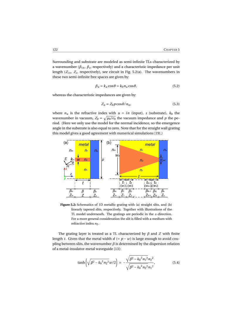
122 CHAPTER 5
Surrounding and substrate are modeled as semi-infinite TLs characterized bya wavenumber (βi n , βs , respectively) and a characteristic impedance per unitlength (Zi n , Zs , respectively), see circuit in Fig. 5.2(a). The wavenumbers inthese two semi-infinite free spaces are given by:
βu = ku cosθ = k0nu cosθ, (5.2)
whereas the characteristic impedances are given by:
Zu = Z0p cosθ/nu , (5.3)
where nu is the refractive index with u = i n (input), s (substrate), k0 thewavenumber in vacuum, Z0 = √
µ0/ε0 the vacuum impedance and p the pe-riod. (Here we only use the model for the normal incidence, so the emergenceangle in the substrate is also equal to zero. Note that for the straight wall gratingthis model gives a good agreement with numerical simulations [19].)
Figure 5.2: Schematics of 1D metallic grating with (a) straight slits, and (b)
linearly tapered slits, respectively. Together with illustrations of the
TL model underneath. The gratings are periodic in the x-direction.
For a more general consideration the slit is filled with a medium with
refractive index n2.
The grating layer is treated as a TL characterized by β and Z with finitelength t . Given that the metal width d (= p −w) is large enough to avoid cou-pling between slits, the wavenumber β is determined by the dispersion relationof a metal-insulator-metal waveguide [13]:
tanh
(√β2 −k0
2n22w/2
)= −
√β2 −k0
2n12n2
2√β2 −k0
2n22n1
2, (5.4)
METALLIC GRATINGS WITH TAPERED SLITS 123
which is the dispersion relation for the even mode in MIM (odd mode is not ex-cited here). Then the characteristic impedance per unit length can be expressedas [19]
Z = wβ
ωε0. (5.5)
The tapered grating is modeled as a series of cascaded TLs, with a stair-case multilayer characterized by local widths wi and thicknesses ti (circuit inFig. 5.2(b)). For each multilayer section we can model it as a two-port net-work as above yielding cascaded two-port networks. To calculate the reflectionR and transmission T of the cascaded network one can use ABCD parameters(also known as transfer matrix approach) [28]. The ABCD parameters (M) of thewhole network are a multiplication of each TL in the network:
M =[
Atot Btot
Ctot D tot
]=∏
Mi =∏[
Ai Bi
Ci Di
](5.6)
where
Ai = Di = cos(βi ti ),
Bi = j Zi sin(βi ti ),
Ci = j Yi sin(βi ti ),
(5.7)
with Yi = 1/Zi , (i = 1, 2, · · · , N ). Therefore R and T are expressed respectivelyby:
R =∣∣∣∣m1Yi n −m2
m1Yi n +m2
∣∣∣∣2
(5.8)
T = 4 |Yi n |2 Re(Ys )
|m1Yi n +m2|2 Re(Yi n)(5.9)
where m1 = Atot +Btot Ys , m2 =Ctot +D tot Ys , Yu = 1/Zu , u = i n, s.Upon derivation of Eq. 5.5 uniform electric fields in the slit and negligible
coupling between the slits is assumed [19], so the TL model works well withsmall slit widths (w) and large enough metal widths (d). In addition, diffractionin the surrounding and substrate, and surface modes at the grating planes arenot considered in the TL model, so the period of the grating cannot be largerthan the wavelength.
5.2.3 Results
Enhanced transmission
To start with illustrating the effects of tapering, here we assume surround-ing, substrate and material in the slit to be air. Figure 5.3 shows the calculated

124 CHAPTER 5
TM transmission T with normal incidence (θ = 0) for grating structures with dif-ferent sizes, with both FEM and TL calculations. For the gratings with straightsidewalls FP resonance peaks in (a) and (b) are observed almost at the samewavelengths. This indicates the peaks are mainly related to the size of the slitsgiven that coupling between slits is small. Increasing thickness produces morepeaks analogous to a FP cavity as shown in (c).
For various parameters, the tapered grating leads to a dramatic enhance-ment of the transmission over a broadband wavelength range, comparing thestraight sidewall case (Fig. 5.3, blue curves) with the tapered cases. In addition,we notice that the tapered transmission seems to average the FP resonant peaksfor the non-tapered geometry, leading to nonresonant transmission. This aver-aging effect is clear for the smaller wavelengths, and becomes more pronouncedfor larger wi n (more ‘open’ gratings). Although the averaging effect makes thepeak transmission smaller by tapering, as a return a large transmission is avail-able at wavelengths above the original resonance.
Figure 5.3: Transmission T for gratings with different sizes (i.e. different slit
width wi n and wout , grating period p, slit thickness t ). The solid lines
are from numerical simulation by FEM. The dashed lines are from the
TL model.

METALLIC GRATINGS WITH TAPERED SLITS 125
The plots in Fig. 5.3 show a good agreement between the rigorous full-waveFEM simulations and the TL model. Here, in the TL model 10 layers are usedand already provide a good convergence. More in detail, agreement is better forsmall periods (Fig. 5.3(a)), and for straight slits (blue curves in Fig. 5.3(a), (b)and (c)). The deviation is mainly caused by plasmon modes at the slit corners,which are not taken into account in the TL model. Deviation increases whenwi n increases, since the coupling between slits becomes stronger, and unifor-mity of the E field in the slits diminishes. However, the TL model still predictsthe trend of T very well, except for an overestimation at smaller wavelengths.
The increased transmission can be understood as the impedance at theentrance of the slit is much closer by tapering to the impedance in the in-put medium. Considering the impedance per unit length defined by Eq. 5.5,Z = wβ/(ωε0), obviously it can be tuned by the width w (β is also a functionof w as seen in dispersion relation, Eq. 5.6). To illustrate figure 5.4 shows thenormalized impedance per unit length in the slit to that in surrounding as afunction of the distance away from the exit of slit for a wavelength of 5µm. It isclear that as the entrance is more open the impedance difference between theentrance of the slit and the surrounding becomes smaller. As a consequencemore light is funneled.
Figure 5.4: Normalized impedance in the slit as a function of the distance
away from slit exit at λ = 5µm for different wout with grating period
p = 300nm, slit thickness t = 400nm, and wi n = 30nm. (Normalized to
the impedance per unit length in the surrounding defined by Eq. 5.3.)
Non-varying impedance for wi n = 30nm is due to the straight side-
wall with constant width. For wi n = 160nm, and 290nm impedances
increase towards the entrance, getting close to the impedance in sur-
rounding.
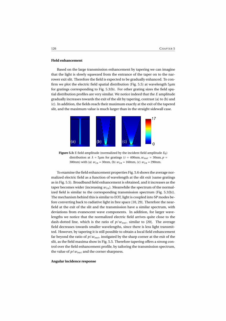
126 CHAPTER 5
Field enhancement
Based on the large transmission enhancement by tapering we can imaginethat the light is slowly squeezed from the entrance of the taper on to the nar-rower exit slit. Therefore the field is expected to be gradually enhanced. To con-firm we plot the electric field spatial distribution (Fig. 5.5) at wavelength 5µmfor gratings corresponding to Fig. 5.3(b). For other grating sizes the field spa-tial distribution profiles are very similar. We notice indeed that the E amplitudegradually increases towards the exit of the slit by tapering, contrast (a) to (b) and(c). In addition, the fields reach their maximum exactly at the exit of the taperedslit, and the maximum value is much larger than in the straight sidewall case.
Figure 5.5: E field amplitude (normalized by the incident field amplitude E0)
distribution at λ = 5µm for gratings (t = 400nm, wout = 30nm, p =300nm) with (a) wi n = 30nm, (b) wi n = 160nm, (c) wi n = 290nm.
To examine the field enhancement properties Fig. 5.6 shows the average nor-malized electric field as a function of wavelength at the slit exit (same gratingsas in Fig. 5.5). Broadband field enhancement is obtained, and it increases as thetaper becomes wider (increasing wi n). Meanwhile the spectrum of the normal-ized field is similar to the corresponding transmission spectrum (Fig. 5.3(b)).The mechanism behind this is similar to EOT, light is coupled into SP modes be-fore converting back to radiative light in free space [10, 29]. Therefore the near-field at the exit of the slit and the transmission have a similar spectrum, withdeviations from evanescent wave components. In addition, for larger wave-lengths we notice that the normalized electric field arrives quite close to thedash-dotted line, which is the ratio of p/wout , similar to [20]. The averagefield decreases towards smaller wavelengths, since there is less light transmit-ted. However, by tapering it is still possible to obtain a local field enhancementfar beyond the ratio of p/wout , instigated by the sharp corner at the exit of theslit, as the field maxima show in Fig. 5.5. Therefore tapering offers a strong con-trol over the field enhancement profile, by tailoring the transmission spectrum,the value of p/wout and the corner sharpness.
Angular incidence response

METALLIC GRATINGS WITH TAPERED SLITS 127
Figure 5.6: Average E field amplitude (normalized by the incident filed am-
plitude E0) versus wavelength at the exit of slit for gratings (t =400nm, wout = 30nm, p = 300nm) with different widths: wi n = 30nm
(blue), wi n = 160nm (green), and wi n = 290nm (red).
We compare the angular response of the straight sidewall gratings (Fig. 5.7(a))with the tapered gratings (Fig. 5.7(b)). For the straight sidewall (Fig. 5.7(a)) weobserve that the transmission gradually increases with the angle, and reachesits maximum near the dashed line around 80◦, which is the brewster angle θB
determined by impedance matching between the surrounding and the straightslit when [19]:
cosθB = βw
k0p. (5.10)
This equation yields from equality between Eqs. 5.3 and 5.5 (impedance match-ing between the mode propagating in straight sidewall slit and light in the sur-rounding air) which is the requirement for no reflection, i.e. setting Eq. 5.8 to bezero.
For the tapered case (Fig. 5.7(b) and (c)) we see that the overall transmissionis significantly larger, which benefits from the gradually reduced impedance to-wards the entrance. In addition, we still observe brewster angle behavior, i.e.the transmission increases with incident angle, as an extra impedance match-ing benefit by tilting the incident light.
Substrate influence
In experimental realizations a different substrate may be necessary. Ourcalculations show the validity of the tapering idea for ns 6= ni , except thatthe transmission at larger wavelength is determined by that of light througha semi-infinite surrounding and substrate according to Fresnel’s law (T =

128 CHAPTER 5
Figure 5.7: Angular response for gratings (t = 400nm, p = 300nm, wout =30nm) with (a) wi n = 30nm (straight sidewalls), (b) wi n = 160nm and
(c) wi n = 290nm (tapered sidewalls). The dashed line in (a) is the plas-
monic brewster angle.
4ns ni n/(ns +ni n)2). To illustrate Fig. 5.8 shows an example with the refractiveindex of substrate equal to 2 for a grating: p = 100nm, t = 200nm, wout = 20nm.The transmission increases with increasing entrance slit width. Meanwhile thethree transmission curves approach the dashed line, which is the transmissionvalue between two semi-infinite free spaces.
5.3 2D gratings
In some applications, like photovoltaics, polarization independence is alwaysdesired. However for the 1D grating considered above, EOT is only observedunder TM-polarized illumination. To make it independent from polarizationwe have to consider 2D gratings. Mimicking the 1D grating above, two differ-ent classes are produced, one is a metal film with hole array, the other is anarray with some isolated metal (e.g. as depicted in Fig. 5.9). As introduced insection 5.1, there is always a cutoff wavelength for a single hole. Although peri-

METALLIC GRATINGS WITH TAPERED SLITS 129
Figure 5.8: Transmission for gratings (t = 200nm, p = 100nm, wout = 20nm)
on a substrate with refractive index 2 with different wi n = 20nm,
55nm, and 90nm. The dashed line is transmission through an inter-
face between air and a substrate with refractive index 2. The dashed
line defines the maximum of the transmission via Fresnel reflection.
odicity will enhance the transmission at EOT peaks, from Eq. 5.1 one derives forthe maximum peak positions λ
λ= p
i 2 + j 2
√εmεd
εm +εd< p
pεd = nd p, (5.11)
so that the peaks will not appear for larger wavelengths, transmission will de-crease. Therefore here we only give a 2D grating example without cutoff asshown in Fig. 5.9.
Figure 5.9: Schematics of 2D metallic grating with perpendicular tapered slits,
which is insensitive to the light polarization.
Here we only consider normal incidence. The two directions of slits have thesame size parameters as the 1D slits of the previous section. Only one polariza-tion parallel to the slits is investigated because of the polarization insensitivity
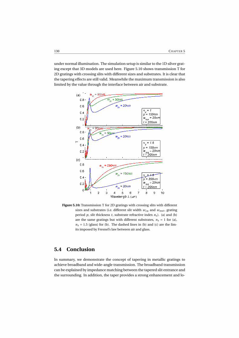
130 CHAPTER 5
under normal illumination. The simulation setup is similar to the 1D silver grat-ing except that 3D models are used here. Figure 5.10 shows transmission T for2D gratings with crossing slits with different sizes and substrates. It is clear thatthe tapering effects are still valid. Meanwhile the maximum transmission is alsolimited by the value through the interface between air and substrate.
Figure 5.10: Transmission T for 2D gratings with crossing slits with different
sizes and substrates (i.e. different slit width wi n and wout , grating
period p, slit thickness t , substrate refractive index ns ). (a) and (b)
are the same gratings but with different substrates, ns = 1 for (a),
ns = 1.5 (glass) for (b). The dashed lines in (b) and (c) are the lim-
its imposed by Fresnel’s law between air and glass.
5.4 Conclusion
In summary, we demonstrate the concept of tapering in metallic gratings toachieve broadband and wide-angle transmission. The broadband transmissioncan be explained by impedance matching between the tapered slit entrance andthe surrounding. In addition, the taper provides a strong enhancement and lo-

METALLIC GRATINGS WITH TAPERED SLITS 131
calization of light at the exit of the slit, useful for applications such as nonlin-ear optics, light harvesting, sensing, emission enhancement etc. The TL modelgives a very efficient characterization of the tapering effect, therefore it can beused to assist more complex designs, e.g. with parabolic shapes. The transmis-sion at smaller wavelengths is further improved by tilting the incident light, giv-ing rise to a plasmonic Brewster type effect. Finally we also demonstrate a polar-ization independent 2D grating with normally crossing slits, where the taperingeffects are still valid.
132 CHAPTER 5
References
[1] H. A. Bethe. Theory of diffraction by small holes. Physical Review, 66(7-8):163–182, 1944.
[2] T. W. Ebbesen, H. J. Lezec, H. F. Ghaemi, T. Thio, and P. A. Wolff. Extraor-dinary optical transmission through sub-wavelength hole arrays. Nature,391(14):667–669, 1998.
[3] H. Ghaemi, T. Thio, D. Grupp, T. Ebbesen, and H. Lezec. Surface plasmonsenhance optical transmission through subwavelength holes. Physical Re-view B, 58(11):6779–6782, 1998.
[4] L. Martín-Moreno, F. J. García-Vidal, H. J. Lezec, K. M. Pellerin, T. Thio, J. B.Pendry, and T. W. Ebbesen. Theory of extraordinary optical transmissionthrough subwavelength hole arrays. Physical Review Letters, 86:1114–1117,2001.
[5] K. J. K. Koerkamp, S. Enoch, F. B. Segerink, N. F. Van Hulst, and L. Kuipers.Strong influence of hole shape on extraordinary transmission through peri-odic arrays of subwavelength holes. Physical Review Letters, 92(18):183901,2004.
[6] K. L. Van der Molen, K. J. K. Koerkamp, S. Enoch, F. B. Segerink, N. F.Van Hulst, and L. Kuipers. Role of shape and localized resonances in ex-traordinary transmission through periodic arrays of subwavelength holes:experiment and theory. Physical Review B, 72(4):045421, 2005.
[7] A. Degiron and T. W. Ebbesen. The role of localized surface plasmon modesin the enhanced transmission of periodic subwavelength apertures. Journalof Optics A: Pure and Applied Optics, 7(2):S90–S96, 2005.
[8] J. Porto, F. García-Vidal, and J. Pendry. Transmission resonances on metallicgratings with very narrow slits. Physical Review Letters, 83(14):2845–2848,1999.
[9] Q. Cao and P. Lalanne. Negative role of surface plasmons in the transmissionof metallic gratings with very narrow slits. Physical Review Letters, 88(5):3–6, 2002.
[10] X. R. Huang, R. W. Peng, and R. H. Fan. Making metals transparent for whitelight by spoof surface plasmons. Physical Review Letters, 105(24):1–4, 2010.
[11] F. Yang and J. Sambles. Resonant transmission of microwaves through anarrow metallic slit. Physical Review Letters, 89(6):5–7, 2002.
METALLIC GRATINGS WITH TAPERED SLITS 133
[12] J. Suckling, A. Hibbins, M. Lockyear, T. Preist, J. Sambles, and C. Lawrence.Finite conductance governs the resonance transmission of thin metal slits atmicrowave frequencies. Physical Review Letters, 92(14):1–4, 2004.
[13] E. N. Economou. Surface plasmons in thin films. Physical Review, 182:539–554, 1969.
[14] A. G. Brolo, E. Arctander, R. Gordon, B. Leathem, and K. L. Kavanagh.Nanohole-enhanced Raman scattering. Nano Letters, 4(10):2015–2018,2004.
[15] A. G. Brolo, R. Gordon, B. Leathem, and K. L. Kavanagh. Surface plas-mon sensor based on the enhanced light transmission through arrays ofnanoholes in gold films. Langmuir, 20(12):4813–4815, 2004.
[16] R. Gordon, D. Sinton, K. L. Kavanagh, and A. G. Brolo. A new generation ofsensors based on extraordinary optical transmission. Accounts of ChemicalResearch, 41(8):1049–1057, 2008.
[17] M. Schnell, P. Alonso-González, L. Arzubiaga, F. Casanova, L. E. Hueso,A. Chuvilin, and R. Hillenbrand. Nanofocusing of mid-infrared energy withtapered transmission lines. Nature Photonics, 5:283–287, 2011.
[18] H. A. Atwater and A. Polman. Plasmonics for improved photovoltaic devices.Nature Materials, 9:205–214, 2010.
[19] A. Alù, G. D’ Aguanno, N. Mattiucci, and M. Bloemer. Plasmonic brew-ster angle: broadband extraordinary transmission through optical gratings.Physical Review Letters, 106(12):1–4, 2011.
[20] G. Subramania, S. Foteinopoulou, and I. Brener. Nonresonant broadbandfunneling of light via ultrasubwavelength channels. Physical Review Let-ters, 107(16):1–5, 2011.
[21] T. Søndergaard, S. I. Bozhevolnyi, S. M. Novikov, J. Beermann, E. De-vaux, and T. W. Ebbesen. Extraordinary optical transmission enhanced bynanofocusing. Nano Letters, 10(8):3123–8, 2010.
[22] J. Beermann, T. Søndergaard, S. M. Novikov, S. I. Bozhevolnyi, E. Devaux,and T. W. Ebbesen. Field enhancement and extraordinary optical trans-mission by tapered periodic slits in gold films. New Journal of Physics,13(6):063029, 2011.
[23] T. Søndergaard, S. I. Bozhevolnyi, J. Beermann, S. M. Novikov, E. Devaux,and T. W. Ebbesen. Extraordinary optical transmission with tapered slits:effect of higher diffraction and slit resonance orders. 29(1):130–137, 2012.

134 CHAPTER 5
[24] Comsol Multiphysics. http://www.comsol.com.
[25] E. D. Palik. Handbook of Optical Constants of Solids. Academic, New York,1985.
[26] F. Medina, F. Mesa, and R. Marqués. Extraordinary transmission througharrays of electrically small holes from a circuit theory perspective. IEEETransactions on Microwave Theory and Techniques, 56(12):3108–3120,2008.
[27] V. Delgado and R. Marqu. Surface impedance model for extraordi-nary transmission in 1D metallic and dielectric screens. Optics Express,19(25):25290–25297, 2011.
[28] D. M. Pozar. Microwave Engineering. J. Wiley, 12005.
[29] W. L. Barnes, A. Dereux, and T. W. Ebbesen. Subwavelength optics. Nature,424:824–830, 2003.
6Conclusions and perspectives
6.1 Conclusions
Metallic nanostructures have the ability to concentrate and manipulate light atthe nanoscale. In this work we have investigated the potential of using metallicnanostructures to boost light harvesting in OSCs.
We performed systematic numerical studies on the effects of small particlesin absorbing devices. To take advantage of the dipolar localized plasmon modein metallic nanoparticles, it is better to embed them directly in the active layer,since the scattering effects of small particles are negligible. Based on a 2D modelfor organic solar cells with metallic nanowires, we analyzed the influence of par-ticle spacing and size. With optimized size and density a best enhancementfactor around 1.56 for absorption (from 30% to 47%) and 1.63 for current den-sity (from 6.7mA/cm2 to 10.9mA/cm2) is achievable, bringing the thin solar cellclose to the performance of a much thicker cell without nanowires. Enhance-ment is mainly due to the near-field enhancement concomitant with the local-ized plasmon mode excitation. Meanwhile, the interaction between nanowireshas a strong influence on the near-field mode profile. To avoid direct contactbetween metal and the active material, a coating buffer will be needed. We no-ticed that a silica coating strongly declines the absorption enhancement as thecoating thickness increases. However other researchers have shown that thismay be alleviated by using a higher index coating material [1].

136 CONCLUSIONS
Since metallic nanowires are sensitive to the polarization of light (LSP modecan only be excited with TM polarization), we studied 2D particle arrays em-bedded in the active layer, resulting in significant absorption and current den-sity enhancements. Material studies for the spherical particles concluded thatAl and Ag provide comparable absorption and current density enhancements.In contrast, Au particles give a small enhancement; its localized plasmon is ex-cited at larger wavelengths, and one observes large losses in the particles due tointerband transitions. Experiments carried out by colleagues at imec with smallmolecules (CuPc and SubPc) have confirmed that the near-field enhancementof small Ag particles boosts the light harvesting, in agreement with our simula-tions.
Many experiments in the literature have particles embedded in the bufferlayer (PEDOT:PSS), next to the active layer. From the viewpoint of optics, ourstudies point to a reduction in absorption, instead of an efficiency enhancementobserved in some experiments. Therefore these enhancements with particles ina buffer layer should be attributed to electronic effects, and various experimentspoint to similar findings.
We also demonstrated the feasibility of scattering by larger MNPs to enhancethe efficiency of OSCs. We introduced Ag NP arrays with a square lattice ontop of OSCs. Light can be effectively trapped inside the active layer, improvingthe light harvesting. Further improvement can be achieved by filling the spacebetween particles in the NP array with a medium.
Another aspect associated with metallic nanostructures is the excitation ofsurface modes, which also provides pathways ways for extra light harvesting.We investigated the influence of combined 1D gratings, composed of both frontand back gratings, on the absorption in the active layer of OSCs. To achievea superposition of contributions from front and back gratings we introduced ahalf period offset between the gratings. The modes in these devices are of mixedcharacter, comprising both localized and propagating properties. With an op-timal period and grating geometry, enhancement factors of 1.35 and 1.42 arerespectively reached for absorption and current density enhancements for TMpolarized normal incident light. Two different kinds of Bloch modes, namelybright and dark modes (symmetrical versus asymmetrical magnetic field pro-file), exist in the grating structures due the periodicity. The dark mode can onlybe excited with tilted incident light, which leads to a mechanism for absorptionover a larger angular range. The absorption and current density enhancementsare boosted further with tilted incident light around 10◦. Furthermore, we foundthat with TE polarized light the combined gratings do not decrease the observedenhancement strongly. Finally, we also performed investigations on 2D Ag nan-odisk arrays in the buffer layer, to obtain a polarization insensitive structure. Aconsiderable current density enhancement factor around 1.21 was observed.

CONCLUSIONS 137
To further explore nanostructured electrodes, we studied metallic gratingswith tapered openings. There are always modes available in slits with straightsidewalls, however these often lead to narrow Fabry-Perot type resonances. Bytapering the slits we observe a broadband and wide-angle transmission, whichis attributed to impedance matching between the tapered slit entrance and thesurrounding, and is efficiently described by a transmission line model. In ad-dition, the taper provides a strong enhancement and localization of light at theexit of the slit, useful for applications such as nonlinear optics, light harvesting,sensing, emission enhancement etc. The transmission at smaller wavelengthsis further improved by tilting the incident light, giving rise to a plasmonic Brew-ster type effect. Finally, we demonstrated these tapering ideas in a polarizationindependent 2D grating with normally crossing slits.
6.2 Perspectives
In this work theoretical studies have shown the promise of incorporating metal-lic structures into solar cell devices. However, the required nanoscale precisionmakes fabrication difficult to control.
For the use of particles for light harvesting, somewhat easier geometries tofabricate should be considered in future work. One possible way is to employthe particles as scatterers at the front or back, leading to larger sizes which arenecessary for prominent scattering. We have demonstrated this configurationin chapter 3 by introducing large NP arrays on the top surface of OSCs, how-ever the enhancement factor is still not optimized completely. Meanwhile thereare still other shapes of particles not yet investigated here. These configura-tions have been investigated in silicon thin-film solar cells with considerablelight harvesting improvement [2–4]. However, for this kind of thin-film cells theactive layer thickness is usually not smaller than 300nm, thus scattered light canbe coupled to the guided modes in the layer structure. For organic solar cellsone needs a thinner layer thickness, and one is confronted with a lower refrac-tive index reducing the amount of guided modes. In the end, strongly confinedplasmonic light enhancement will become useful when very thin organic layersare considered, which is for current fabrication methods still state-of-the-art orbeyond. We remark also that the electronic properties of metallic nanostruc-tures inside solar cells offer another pathway for future research and optimiza-tion.
Other promising configurations could employ the hybrid element approach,like the combined gratings we proposed. Indeed, combining benefits at vari-ous wavelength ranges from different structures would further boost the overalllight harvesting, leading closer towards the ultimate device absorption.
Non-resonant devices, such as the tapered structures, present a comple-

138 CONCLUSIONS
mentary, and less studied, approach to enhance the light-matter interaction.Instead of adding resonances to the spectrum, here one aims to have a rela-tively feature-less, but broadband response, which is achievable in selected ge-ometries, and still needs further investigation.

CONCLUSIONS 139
References
[1] J. Y. Lee and P. Peumans. The origin of enhanced optical absorption in solarcells with metal nanoparticles embedded in the active layer. Optics Express,18(10):10078–87, 2010.
[2] Y. A. Akimov, W. S. Koh, and K. Ostrikov. Enhancement of optical absorptionin thin-film solar cells through the excitation of higher-order nanoparticleplasmon modes. Optics Express, 17(12):10195–205, 2009.
[3] Y. A. Akimov and W. S. Koh. Design of Plasmonic Nanoparticles for Effi-cient Subwavelength Light Trapping in Thin-Film Solar Cells. Plasmonics,6(1):155–161, 2010.
[4] F.-J. Tsai, J.-Y. Wang, J.-J. Huang, Y.-W. Kiang, and C. C. Yang. Absorption en-hancement of an amorphous Si solar cell through surface plasmon-inducedscattering with metal nanoparticles. Optics Express, 18(102):A207–20, 2010.
