null synthesis and implementation of cylindrical
TRANSCRIPT
Null Synthesis and Implementation
of Cylindrical Microstrip Patch
Arrays
by
Philip Niemand
Submitted as partial fulfilment of the requirements for the degree
Ph.D (Electronic Engineering)in the
Faculty of Engineering, Built Environment and Information Technology
University of Pretoria
Pretoria
November 2004
UUnniivveerrssiittyy ooff PPrreettoorriiaa eettdd –– NNiieemmaanndd,, PP ((22000055))

Null Synthesis and Implementation of Cylindrical Microstrip Patch Arrays
Philip Niemand
Prof. J. Joubert
Prof. J.W. Odendaal
Department of Electrical, Electronic and Computer Engineering
Ph.D (Electronic Engineering)
As the wireless communications networks expand, the number of both unwanted directional inter-
ferences and strong nearby sources increase, which degrade system performance. The signal-to-
interference ratio (SIR) can be improved by using multiple nulls in the directions of the interferences
while maintaining omnidirectional coverage in the direction of the network users. For the commu-
nication system considered, the interferences are static and their spatial positions are known. A
non-adaptive antenna array is needed to provide spatial filtering in a static wireless environment.
Omnidirectional arrays, such as cylindrical arrays, are the most suitable to provide the omnidirec-
tional coverage and are capable of suppressing interferences when nulls are inserted in the radiation
pattern.
In this thesis, a cylindrical microstrip patch antenna array is investigated as an antenna to provide
an omnidirectional radiation pattern with nulls at specified angular locations to suppress interference
from directional sources. Three null synthesis methods are described and used to provide the om-
nidirectional array pattern with nulls using the radiation characteristics of the cylindrical microstrip
patch antenna elements. The orthogonal projection method is extended to incorporate the directive
radiation patterns of the cylindrical microstrip patch elements. Using this method, an optimal pat-
tern that minimises the squared pattern error with respect to the ideal pattern is obtained. Instead
of only minimising the array pattern error, a multi-objective optimisation approach is also followed.
The objective weighting method is applied in null pattern synthesis to improve the amplitude pat-
tern characteristics of the cylindrical patch arrays. As a third null synthesis technique, a constraint
optimisation method is applied to obtain a constrained pattern with the desired amplitude pattern
characteristics. The influence of the array attributes on the characteristics of the amplitude patterns
obtained from the null synthesis methods, is also studied.
In addition, the implementation of the cylindrical microstrip patch array is investigated. The influence
of the mutual coupling on the characteristics of the null patterns of the cylindrical patch arrays is
investigated utilising simulations and measurements. A mutual coupling compensation technique is
used to provide matched and equal driving impedances for all the patch antenna elements given a
required set of excitations. Test cases in which this technique is used, are discussed and the consequent
improvements in the bandwidth and reflection coefficient of a linear patch arrays are shown. The
characteristics of the resulting null pattern for the cylindrical microstrip patch array is also improved
using the compensation technique.
Keywords: antenna, microstrip, array, cylindrical, null, synthesis, orthogonal, projection, coupling,
compensation.
UUnniivveerrssiittyy ooff PPrreettoorriiaa eettdd –– NNiieemmaanndd,, PP ((22000055))

Acknowledgements
First of all I would like to dedicate this thesis to my Father in heaven who made it
possible through his many blessings.
I would also like to thank my wife, Willemien, for her patience and support.
Special thanks to Johan Joubert and Wimpie Odendaal for their guidance and friend-
ship.
Furthermore, I would like to thank everybody whose support and friendship made this
thesis possible.
UUnniivveerrssiittyy ooff PPrreettoorriiaa eettdd –– NNiieemmaanndd,, PP ((22000055))

CONTENTS
1 INTRODUCTION 1
1.1 Background . . . . . . . . . . . . . . . . . . . . . . . . . . . . . . . . . 1
1.2 Contributions . . . . . . . . . . . . . . . . . . . . . . . . . . . . . . . . 5
1.3 Methodology . . . . . . . . . . . . . . . . . . . . . . . . . . . . . . . . 6
1.4 Layout of thesis . . . . . . . . . . . . . . . . . . . . . . . . . . . . . . . 7
2 BACKGROUND 8
2.1 Characteristics of a cylindrical microstrip patch . . . . . . . . . . . . . 9
2.1.1 Cavity model for cylindrical microstrip patches . . . . . . . . . 9
2.1.2 Radiated fields . . . . . . . . . . . . . . . . . . . . . . . . . . . 11
2.1.3 Axial polarisation . . . . . . . . . . . . . . . . . . . . . . . . . . 13
2.1.4 Circumferential polarisation . . . . . . . . . . . . . . . . . . . . 13
2.1.5 Characteristics of the radiation patterns . . . . . . . . . . . . . 13
2.2 Cylindrical array pattern . . . . . . . . . . . . . . . . . . . . . . . . . . 16
2.2.1 Equally spaced cylindrical arrays . . . . . . . . . . . . . . . . . 22
2.3 Null synthesis techniques . . . . . . . . . . . . . . . . . . . . . . . . . . 25
2.3.1 Definitions of parameters in null synthesis . . . . . . . . . . . . 25
2.3.2 Superposition of sequence excitations . . . . . . . . . . . . . . . 25
i
UUnniivveerrssiittyy ooff PPrreettoorriiaa eettdd –– NNiieemmaanndd,, PP ((22000055))

CONTENTS
2.3.3 Fourier approximation of an ideal pattern . . . . . . . . . . . . 28
2.3.4 Orthogonal projection method . . . . . . . . . . . . . . . . . . . 30
2.3.5 Pattern synthesis with null constraints . . . . . . . . . . . . . . 39
2.3.6 Constrained minimisation with Lagrange multipliers . . . . . . . 41
2.3.7 Constrained optimisation techniques . . . . . . . . . . . . . . . 42
2.4 Mutual coupling compensation . . . . . . . . . . . . . . . . . . . . . . . 44
2.4.1 Minimising the mutual coupling effects . . . . . . . . . . . . . . 45
2.4.2 Compensation using coupling and impedance matrixes . . . . . 45
2.4.3 Modification of the driving impedances . . . . . . . . . . . . . . 50
2.5 Summary . . . . . . . . . . . . . . . . . . . . . . . . . . . . . . . . . . 51
3 NULL SYNTHESIS 53
3.1 Orthogonal projection method . . . . . . . . . . . . . . . . . . . . . . . 54
3.1.1 Modification of the orthogonal base . . . . . . . . . . . . . . . . 54
3.1.2 Results of the projection method . . . . . . . . . . . . . . . . . 55
3.2 Objective weighting method . . . . . . . . . . . . . . . . . . . . . . . . 63
3.2.1 Performance function and Pareto optimality . . . . . . . . . . . 63
3.2.2 Results of the objective weighting method . . . . . . . . . . . . 65
3.3 Constrained optimisation . . . . . . . . . . . . . . . . . . . . . . . . . . 73
3.3.1 Results of the constrained optimisation . . . . . . . . . . . . . . 73
3.4 Comparison of null synthesis methods . . . . . . . . . . . . . . . . . . . 78
3.5 Multiple null synthesis . . . . . . . . . . . . . . . . . . . . . . . . . . . 81
3.6 Influences of the antenna element characteristics . . . . . . . . . . . . . 84
3.6.1 Influence of the dielectric constant . . . . . . . . . . . . . . . . 84
Department of Electrical, Electronic and Computer Engineering ii
UUnniivveerrssiittyy ooff PPrreettoorriiaa eettdd –– NNiieemmaanndd,, PP ((22000055))
CONTENTS
3.6.2 Influence of the height of the substrate . . . . . . . . . . . . . . 85
3.7 Results for various null positions . . . . . . . . . . . . . . . . . . . . . . 90
3.8 Summary . . . . . . . . . . . . . . . . . . . . . . . . . . . . . . . . . . 92
4 IMPLEMENTATION OF CYLINDRICAL MICROSTRIP PATCH
ARRAYS 96
4.1 Design of cylindrical microstrip patch element . . . . . . . . . . . . . . 98
4.2 Effect of mutual coupling . . . . . . . . . . . . . . . . . . . . . . . . . . 103
4.2.1 Effect of mutual coupling for linear patch arrays . . . . . . . . . 103
4.2.2 Effect of mutual coupling on the amplitude pattern of cylindrical
patch arrays . . . . . . . . . . . . . . . . . . . . . . . . . . . . . 105
4.3 Mutual coupling compensation . . . . . . . . . . . . . . . . . . . . . . . 114
4.3.1 Mutual coupling compensation for linear patch arrays . . . . . . 114
4.3.2 Mutual coupling compensation for cylindrical arrays . . . . . . . 115
4.4 Test cases . . . . . . . . . . . . . . . . . . . . . . . . . . . . . . . . . . 119
4.4.1 Linear patch array test case . . . . . . . . . . . . . . . . . . . . 119
4.4.2 Cylindrical patch array test case . . . . . . . . . . . . . . . . . . 120
4.5 Summary . . . . . . . . . . . . . . . . . . . . . . . . . . . . . . . . . . 129
5 CONCLUSIONS 134
5.1 Null synthesis using cylindrical microstrip patch arrays . . . . . . . . . 134
5.2 Implementation of cylindrical microstrip patch arrays . . . . . . . . . . 137
REFERENCES 141
Department of Electrical, Electronic and Computer Engineering iii
UUnniivveerrssiittyy ooff PPrreettoorriiaa eettdd –– NNiieemmaanndd,, PP ((22000055))
CHAPTER 1
INTRODUCTION
1.1 Background
The demand for wireless communications services is growing at an extensive rate all
over the world. The intensive development and wide application of new generations of
personal communication systems and wireless local systems, have increased the need
for new antenna designs [1]. As the wireless communications networks expand, the
number of both unwanted directional interferences and strong nearby sources increase,
which degrade system performance. Optimal antenna arrays play an important role in
the improvement of communications systems by providing increased coverage through
antenna gain control and interference rejection [2, 3]. A system consisting of an ar-
ray and a processor can perform filtering in both space and frequency to reduce the
sensitivity of the system to interfering directional sources.
There are many requirements that new communications systems pose on antennas. The
most common are low cost, low weight and compact designs with high-performance
radiation and impedance characteristics. Therefore uplink and downlink antennas
undergo a lot of modifications and performance improvement [1]. In many wireless
communications systems, the signal-to-interference ratio (SIR) is improved by using
multiple nulls in the directions of the interferences while maintaining omnidirectional
coverage in the direction of the network users. The nulls in the radiation pattern may
be used to reduce the interference from strong nearby sources as well as co-channel
interference by introducing nulls in the directions of surrounding communication sys-
1
UUnniivveerrssiittyy ooff PPrreettoorriiaa eettdd –– NNiieemmaanndd,, PP ((22000055))
Chapter 1 Introduction
tems.
For the communication system considered in this thesis, the interferences are static
and their directions of arrival are known. A non-adaptive antenna array is needed to
provide the spatial filtering in a static wireless environment. Multi-path scenarios and
space-time filtering via an adaptive array are therefore not addressed.
Omnidirectional arrays, such as cylindrical arrays, are the most suitable to provide the
omnidirectional coverage and are capable of suppressing interferences when nulls are
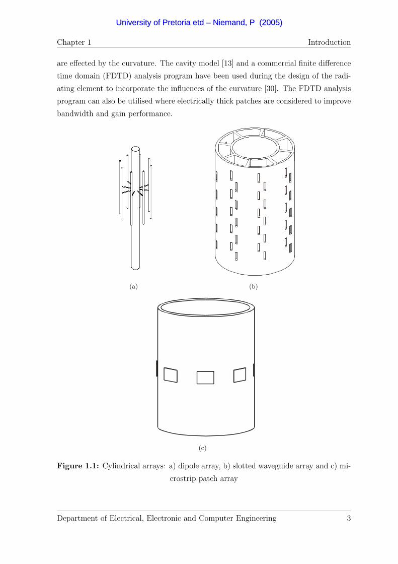
inserted in the radiation pattern. Some examples of cylindrical arrays are shown in
Figure 1.1.
Microstrip antennas, which the work in this thesis will focus on, are popular compo-
nents in modern systems, since they are low in profile, light in weight and well suited
for integration with microwave integrated circuits. They can also be made confor-
mal to non-planar surfaces such as cylinders to form cylindrical arrays as shown in
Figure 1.1(c).
This type of cylindrical array is also classified under conformal arrays of which the
analysis and design can be divided into three areas [4]:
1. the analysis of the antenna element radiation pattern,
2. the array pattern analysis and synthesis to obtain the element excitations, and
3. the design of the radiators and the feed network to obtain the desired excitations.
The analysis of cylindrical microstrip patch antennas and arrays have been discussed
in many publications [5–31]. The cavity model theory, method of moments, geometric
theory of diffraction (GTD) and finite-element method have all been applied to obtain
the resonant frequency, impedance behaviour and/or radiation pattern of a rectangular
microstrip patch on a conducting cylinder. For electrically thin substrates, the cavity
model has been shown to be sufficient to compute the characteristics of the patch an-
tenna [23,24,29]. Hybrid modes are excited for electrically thick patches which require
more accurate analysis methods [14]. When the radius of the cylinder is much larger
than the operating wavelength, the effect of the curvature on the characteristics of the
patch antennas may be neglected. For radii comparable to the operating wavelength,
the input impedance, resonant frequency and radiation pattern of the patch antenna
Department of Electrical, Electronic and Computer Engineering 2
UUnniivveerrssiittyy ooff PPrreettoorriiaa eettdd –– NNiieemmaanndd,, PP ((22000055))
Chapter 1 Introduction
are effected by the curvature. The cavity model [13] and a commercial finite difference
time domain (FDTD) analysis program have been used during the design of the radi-
ating element to incorporate the influences of the curvature [30]. The FDTD analysis
program can also be utilised where electrically thick patches are considered to improve
bandwidth and gain performance.
(a) (b)
(c)
Figure 1.1: Cylindrical arrays: a) dipole array, b) slotted waveguide array and c) mi-
crostrip patch array
Department of Electrical, Electronic and Computer Engineering 3
UUnniivveerrssiittyy ooff PPrreettoorriiaa eettdd –– NNiieemmaanndd,, PP ((22000055))
Chapter 1 Introduction
Previously, cylindrical microstrip patch arrays were extensively used for omnidirecitonal
coverage [9,18] and the formation of beams in the far field radiation pattern [1,32–40].
Many techniques for the introduction of nulls in the far field radiation patterns of
cylindrical arrays can be found in the open literature [41, 43–55]. Lim [43] proposed
the introduction of a single null into an omnidirectional pattern by approximating an
abrupt phase reversal in the phase pattern of the array. This phase reversal in the
specified direction of the null also minimised the null width. An orthogonal projection
method was introduced by Vescovo [50,51] to synthesise a desired radiation pattern for
an equally spaced cylindrical array. Abele et al [53, 54] combined these two methods
to synthesise multiple nulls in the omnidirectional pattern of a cylindrical array. An
ideal null pattern with constant amplitude and an abrupt phase reversal at the desired
location of each null was used in the orthogonal projection method. The null positions
and depths could be controlled independently and some control could be exercised over
the gain ripple and null width by utilising windowing functions.
All the above methods use radiating elements that are identical in radiation pattern,
polarisation, gain and impedance. In conformal arrays, the elements, and consequently
their radiation patterns, point in different directions and the element pattern cannot be
factorised out of the array pattern to obtain an array factor [4,56,57]. Vescovo [56] also
applied the projection method to an arc array of elements with directional radiation
patterns. After a main beam was formed through the projection method, additional
nulls were introduced in the pattern with null constraints to reduce the side lobe level.
The effect of mutual coupling between elements in an array is one of the most rele-
vant problems in the synthesis of array antennas. Numerous methods to compute or
represent the mutual coupling in linear and cylindrical microstrip patch arrays have
been presented [17, 19, 24, 25, 29, 58–71]. The mutual coupling between the antenna
elements modifies the element excitations and the driving input impedances of the
antenna elements.
For arrays with wide band antenna elements and small mutual coupling between the
elements, the measured radiation pattern characteristics may still be within the desired
characteristics, although the mutual coupling was not taken into account during the
design process of the array [32, 34–37, 39]. On the other hand, the consequent errors
in the element excitations due to high mutual coupling may deteriorate the radiation
pattern. This is especially true for a shaped or scanned beam, if the mutual coupling
Department of Electrical, Electronic and Computer Engineering 4
UUnniivveerrssiittyy ooff PPrreettoorriiaa eettdd –– NNiieemmaanndd,, PP ((22000055))

Chapter 1 Introduction
is not compensated for in the design process [72,73]. For the accurate computation of
the sidelobe levels in a beam pattern, the mutual coupling was taken into account by
Bartolic et al [1].
Null filling and null position errors also occur during null synthesis due to the mutual
coupling [53, 74]. Various authors have presented techniques to compensate for the
mutual coupling effect on a synthesised array pattern [54, 72–86]. At the array feed
port, a mismatch occurs due to coupling [87], which may significantly degrade the
performance of narrowband arrays. The driving impedances of the antenna elements
resulting from radiation pattern correction methods remain unequal and the design of
the feeding and matching network can be complicated. Another solution is to alter the
individual element geometries physically in order to have equal driving impedances for
the required element excitations [88, 89]. This method causes the feeding network to
be much simpler.
1.2 Contributions
In this thesis, a cylindrical microstrip patch antenna array is investigated as an antenna
to provide an omnidirectional radiation pattern with nulls at specified angular locations
to suppress interference from directional sources. The null synthesis for the cylindrical
microstrip patch array is presented by discussing the above three mentioned areas of
array analysis and design.
Three null synthesis methods are described and used to provide the omnidirectional
array pattern with nulls using the radiation characteristics of the cylindrical microstrip
patch antenna elements. The desired element excitations are obtained from:
• the extension of the orthogonal projection method to incorporate the radiation
patterns of the cylindrical microstrip patch antenna elements [90–92],
• the implementation of the objective weighting method for null pattern synthesis,
and
• the application of a constraint optimisation method for the synthesis of null
patterns with specified characteristics [92].
Department of Electrical, Electronic and Computer Engineering 5
UUnniivveerrssiittyy ooff PPrreettoorriiaa eettdd –– NNiieemmaanndd,, PP ((22000055))

Chapter 1 Introduction
In addition, the implementation of the cylindrical microstrip patch array is investigated
by:
• studying the effect of the mutual coupling on the desired null pattern [93, 94],
and
• applying a technique to compensate for the mutual coupling between the cylin-
drical microstrip patch antenna elements to obtain the desired excitations [93,94].
1.3 Methodology
The null synthesis technique of Abele et al [53] is extended to incorporate the di-
rective radiation patterns of the cylindrical microstrip patch elements. Using this
method, an optimal pattern that minimises the squared pattern error with respect
to the ideal pattern is obtained. The orthogonal projection method may not give an
amplitude pattern with the desired characteristics (null depth, null width and ripple
in the omni-region) for certain array configurations. Instead of only minimising the
array pattern error, a multi-objective optimisation approach is followed [95–97]. The
objective weighting method, previously applied in other fields of computational elec-
tromagnetic problems [96,97], is used to improve the amplitude pattern characteristics
of the cylindrical patch arrays.
Previously, constrained optimisation techniques were used to obtain beam patterns
for circular and arc arrays [45, 52]. As a third null synthesis technique, a constraint
optimisation method is applied to obtain a constrained pattern with the desired am-
plitude pattern characteristics. The optimal pattern is used as the starting value for
the optimisation. The influence of the array attributes, such as the number of array el-
ements and the inter-element spacing, on the characteristics of the amplitude patterns
obtained from the null synthesis methods, is also studied.
In the last part of the array synthesis,the implementation of the cylindrical microstrip
patch arrays is investigated. The influence of the mutual coupling on the characteristics
of the null patterns of the cylindrical patch arrays is investigated utilising simulations
and measurements. In a mutual coupling compensation technique, Chen [88,89] varied
the lengths and radii of the dipoles in linear and planar arrays to obtain the desired
Department of Electrical, Electronic and Computer Engineering 6
UUnniivveerrssiittyy ooff PPrreettoorriiaa eettdd –– NNiieemmaanndd,, PP ((22000055))

Chapter 1 Introduction
radiation patterns as well as equal driving impedances for the dipoles. This compen-
sation technique is used to provide matched and equal driving impedances for all the
patch antenna elements given a required set of excitations. The driving impedances are
corrected by adjusting the lengths and feeding points of the individual patches. Util-
ising the compensation technique, the impedances of the microstrip patch antennas in
both the planar and cylindrical arrays are designed to be 50 Ω for the desired element
excitations. The consequent improvements in the bandwidth and reflection coefficient
of a linear patch arrays are discussed. The resulting amplitude pattern for the compen-
sated cylindrical microstrip patch array is also compared with the amplitude pattern
before the compensation, to observe the improvements in the pattern characteristics.
1.4 Layout of thesis
The relevant background to the null synthesis and mutual coupling compensation for a
cylindrical microstrip patch array is given in Chapter 2. An overview of the characteris-
tics of the cylindrical patch antenna element, the null synthesis techniques, the mutual
coupling effects and coupling compensation techniques is given. In Chapter 3, a null
synthesis technique is adapted and extended for a cylindrical microstrip patch array.
Results of the null synthesis techniques are shown and compared for different array
geometries. A technique to compensate for the mutual coupling in both planar and
cylindrical arrays is discussed and applied in Chapter 4. Both simulated and measured
results are shown. Chapter 5 presents the conclusions of the study.
Department of Electrical, Electronic and Computer Engineering 7
UUnniivveerrssiittyy ooff PPrreettoorriiaa eettdd –– NNiieemmaanndd,, PP ((22000055))

CHAPTER 2
BACKGROUND
Microstrip patch antennas can easily be made to conform to cylindrical surfaces to pro-
vide low profile omnidirectional arrays. A specified array pattern can also be obtained
by configuring the geometries of the elements, the array and the cylinder. For a design
procedure, the radiation patterns of the cylindrical patch elements and the array are
needed. The cavity model is well suited to analyse cylindrical patches etched on thin
substrates and to demonstrate the characteristics of these patch antennas. Two linear
polarisations with different radiation characteristics are available when utilising cylin-
drical patches. In the first part of this chapter, the characteristics of the radiated fields
for both polarisations will be discussed. The radiated fields will also be compared for
different substrates and cylinder radii.
Due to the cylindrical configuration of the microstrip patch array, the array is classi-
fied as a cylindrical array. An introduction to cylindrical arrays and equally spaced
cylindrical arrays, will be given. When the elements are equally spaced around the
circumference of the array, the elements can be excited by using phase-sequence exci-
tations. The orthogonal set of excitation vectors resulting from these phase-sequences
may be implemented in a pattern synthesis method to obtain an optimal set of excita-
tions for a required radiation pattern.
The objective in this thesis is to provide an omnidirectional radiation pattern with one
or more nulls at specified angle locations to suppress directional interferences. Differ-
ent techniques have been presented which perform null beam forming or null pattern
synthesis [41,43–55]. In null beam forming, additional nulls are introduced in the beam
8
UUnniivveerrssiittyy ooff PPrreettoorriiaa eettdd –– NNiieemmaanndd,, PP ((22000055))

Chapter 2 Background
pattern, while null pattern synthesis provide omnidirectional coverage with directional
nulls. In this chapter, a discussion on various null synthesis techniques for omnidirec-
tional patterns will be given. These methods determine the element excitations which
provide the required array radiation pattern.
The element excitations are applied to the array by setting either the element currents
or voltages proportional to the excitations. When the mutual coupling between the
antenna elements in the array is not taken into account during the computation of the
excitations, the resulting radiation pattern may be distorted [53,72–74]. Not only does
the coupling deform the array imbedded radiation patterns of the individual elements,
but also modifies the active impedances at the element ports. Consequently, a technique
to compensate for the mutual coupling has to be implemented to obtain the desired
array radiation pattern. Different techniques to compensate for the mutual coupling
during the synthesis process, will also be discussed.
2.1 Characteristics of a cylindrical microstrip patch
Utilising the cavity model for the cylindrical patch antenna, the characteristics of the
patches can be studied. These antennas may be used in two linear polarisations with
different radiation characteristics, which will be discussed in the following paragraphs.
2.1.1 Cavity model for cylindrical microstrip patches
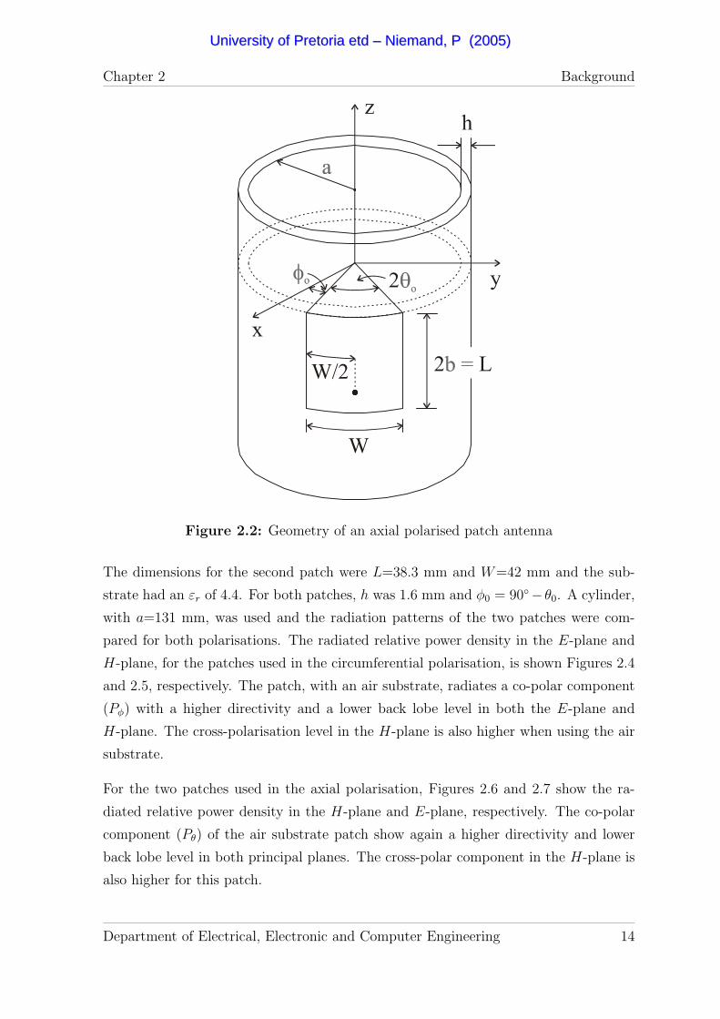
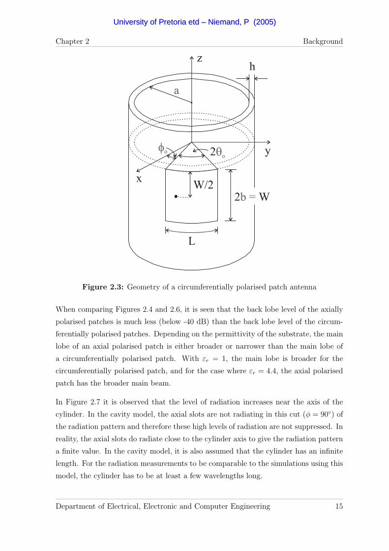
The geometry of a typical cylindrical microstrip patch antenna is shown in Figure 2.1.
2b and 2θ0 define the dimensions of the patch in the z and φ directions, respectively.
φ0 indicates the φ-position of the patch, while a and h define the radius of the cylinder
and height of the substrate, respectively. The position of the coaxial probe feed is
indicated by zf and φf .
One model for the cylindrical patch can be found by regarding the region underneath
the patch as a cavity bounded by four magnetic walls and two electric walls [5,7]. The
E-field in the cavity has only a ρ component, which is independent of ρ if the substrate
is thin (h ¿ a). When the coaxial probe feed is modeled by a current density, with
Department of Electrical, Electronic and Computer Engineering 9
UUnniivveerrssiittyy ooff PPrreettoorriiaa eettdd –– NNiieemmaanndd,, PP ((22000055))

Chapter 2 Background
x
y
z
q
fr
P2qo
fo
x
y
z
a
h
(a+h)ff
zf
2b
Figure 2.1: Geometry of cylindrical microstrip patch antenna
an effective width w, the field in the cavity can be found by a summation over all the
cavity modes [13]:
Eρ = jωµ0
∑m,n
Cmn cos
[mπ
2θ0
(φ− φ0)
]cos
[nπz
2b
], (2.1)
where m and n are the mode indexes. The modal amplitudes Cmn are defined as:
Cmn =w
k2eff − k2
mn
∆m∆n
4(a + h)bθ0
cos
[mπφf
2θ0
]cos
[nπzf
2b
]sinc
[mπw
4(a + h)θ0
], (2.2)
where
∆k =
1, k = 0
2, k 6= 0, (2.3)
Department of Electrical, Electronic and Computer Engineering 10
UUnniivveerrssiittyy ooff PPrreettoorriiaa eettdd –– NNiieemmaanndd,, PP ((22000055))
Chapter 2 Background
kmn =
√(mπ
2(a + h)θ0
)2
+(nπ
2b
)2
, (2.4)
keff = k0
√εr(1− jδeff ), (2.5)
sinc(x) = sin(x)/x, (2.6)
and
k0 = ω√
µ0ε0. (2.7)
µ0 and ε0 are the permeability and permittivity of free space, respectively. The ra-
dial frequency and relative permittivity of the substrate are presented by ω and εr,
respectively. The effective loss tangent δeff represents all the losses in the cavity. The
radiation losses, the losses due to the finite conductivity of the conductor and the
losses in the substrate and through surface waves can be estimated using the method
described in [6]. The modal resonant frequency is given by:
fmn =c
2√
εr
√(mπ
2(a + h)θ0
)2
+(nπ
2b
)2
. (2.8)
When the dimensions 2(a + h)θ0 and 2b of the patch are fixed, Equation 2.8 indicates
that the resonant frequency fmn is independent of the curvature. This assumption is
only valid for thin substrates with h ¿ a [7].
2.1.2 Radiated fields
The four walls of the lossy cavity in the cavity model are considered as the radiating
apertures. Along each wall an equivalent magnetic current can be found from:
M = Eρρ× n, (2.9)
where Eρ is given by Equation 2.1. These radiating walls are also referred to as radi-
ating slots. For these magnetic currents radiating in the vicinity of an infinitely long
cylindrical surface, the far zone radiation field may be obtained using the expressions
Department of Electrical, Electronic and Computer Engineering 11
UUnniivveerrssiittyy ooff PPrreettoorriiaa eettdd –– NNiieemmaanndd,, PP ((22000055))

Chapter 2 Background
presented in [98]. The resulting components of the far zone electric fields for each
cavity mode are given by [13]:
Eθ,mn(r, φ, θ) =E0h
2π2 sin θ
e−jk0r
r
[1− (−1)ne−j2k0b cos θ
]
·∞∑
p=−∞
jp+1ejp(φ−φ0)I(θ0,m,−p)
H(2)p (k0a sin θ)
,
(2.10)
and
Eφ,mn(r, φ, θ) = −jE0h
2π2a
e−jk0r
rI(b, n,−k0 cos θ)
·∞∑
p=−∞
jp+1ejp(φ−φ0)
H(2) ′p (k0a sin θ)
[1− (−1)me−j2pθ0
]
− jE0h
2π2a
e−jk0r
r
cos θ
k0 sin2 θ
[1− (−1)ne−j2k0b cos θ
]
·∞∑
p=−∞
jp+1pejp(φ−φ0)I(θ0,m,−p)
H(2) ′p (k0a sin θ)
,
(2.11)
where
I(b, n, u) =
0∫
−2b
cos(nπz
2b
)e−juzdz, (2.12)
and
I(θ0,m,−p) =
2θ0∫
0
cos
(mπφ
2θ0
)e−jpφdφ. (2.13)
The total radiated field is obtained by a summation over all the cavity modes m,n. The
infinite summations in Equations 2.10 and 2.11 are summations over the cylindrical
modes in which the fields have been expanded. The number of cylindrical modes needed
for convergence depends on the radius of the cylinder and the angle θ, but is usually
less than 2ka [11]. For θ-angles close to the cylinder axis, only a small number of terms
are required.
Department of Electrical, Electronic and Computer Engineering 12
UUnniivveerrssiittyy ooff PPrreettoorriiaa eettdd –– NNiieemmaanndd,, PP ((22000055))
Chapter 2 Background
2.1.3 Axial polarisation
The two slots of the cavity, oriented along the axis of the cylinder, are referred to as
axial slots, while the other two slots, oriented along the circumference of the cylinder,
are called circumferential slots. The patch antenna is axially polarised when fed sym-
metrically in φ, as shown in Figure 2.2. The dominant mode in the cavity will be the
mode m=0, n=1 (TM01). The two circumferential slots are excited equally in phase
and amplitude, while the two axial slots are excited 180 out of phase. The next two
higher order modes will be the TM20 and TM21 modes, with the TM20 mode mainly
contributing to the cross-polar radiation. The TM21 mode contributes weakly to both
the co-polar and cross-polar radiation. The TM01 mode itself gives rise to the Eθ co-
polar radiation with no cross-polar radiation in the symmetry planes. Since the other
higher modes are excited much weaker, most cross-polar radiation originate from the
TM20 mode. A small displacement in φf will cause the TM10 to be excited, which will
result in a higher cross-polarisation level [11]. Special care must be taken when feeding
square patches, since the TM01 and TM10 will have the same resonant frequency.
2.1.4 Circumferential polarisation
The TM10 mode is the dominant mode for a circumferentially polarised patch, since it
is fed symmetrically in z, as shown in Figure 2.3. The Eφ co-polar radiation is given
by the two axial slots excited in phase. The two higher order modes contributing the
most to the radiation are the TM02 and TM12 modes, with the cross-polarisation level
mainly determined by the radiation from the TM02 mode.
2.1.5 Characteristics of the radiation patterns
The radiation pattern of a cylindrical patch depends on the geometries of the cylin-
der (a) and the patch (θ0,b), as well as the characteristics of the substrate (h,εr). A
comparison of the radiation patterns for patches with different substrates is shown in
Figures 2.4 to 2.7. The radiation patterns were determined using the cavity model
(Equations 2.10 and 2.11) at 1.8 GHz.
An air substrate was used for the first patch, with dimensions L=73.6 mm and W=76 mm.
Department of Electrical, Electronic and Computer Engineering 13
UUnniivveerrssiittyy ooff PPrreettoorriiaa eettdd –– NNiieemmaanndd,, PP ((22000055))
Chapter 2 Background
Figure 2.2: Geometry of an axial polarised patch antenna
The dimensions for the second patch were L=38.3 mm and W=42 mm and the sub-
strate had an εr of 4.4. For both patches, h was 1.6 mm and φ0 = 90−θ0. A cylinder,
with a=131 mm, was used and the radiation patterns of the two patches were com-
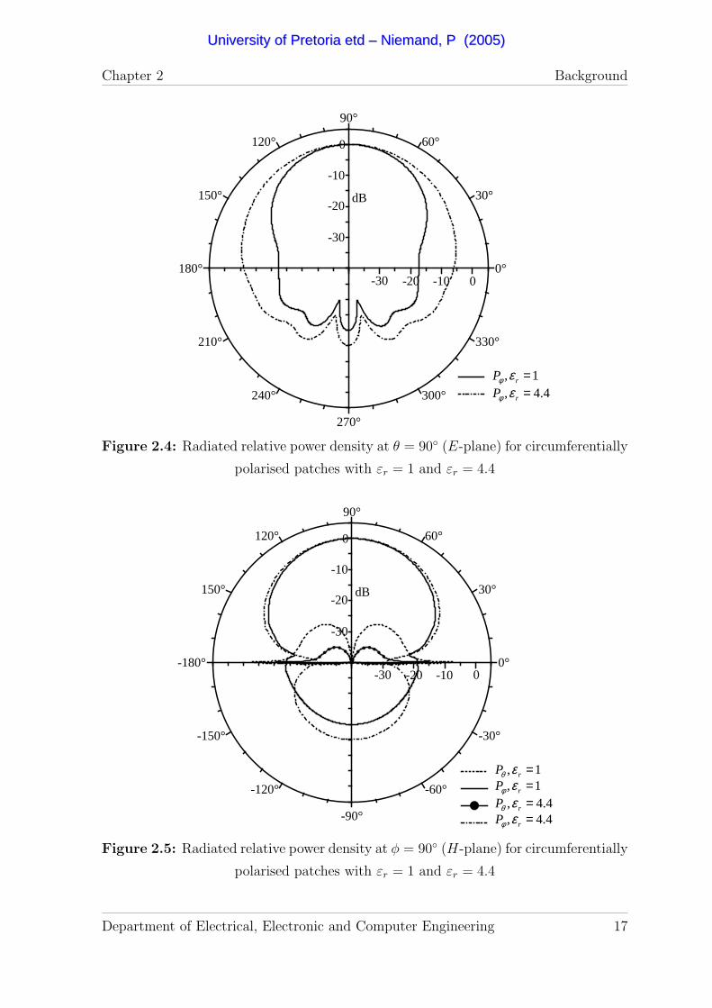
pared for both polarisations. The radiated relative power density in the E-plane and
H-plane, for the patches used in the circumferential polarisation, is shown Figures 2.4
and 2.5, respectively. The patch, with an air substrate, radiates a co-polar component
(Pφ) with a higher directivity and a lower back lobe level in both the E-plane and
H-plane. The cross-polarisation level in the H-plane is also higher when using the air
substrate.
For the two patches used in the axial polarisation, Figures 2.6 and 2.7 show the ra-
diated relative power density in the H-plane and E-plane, respectively. The co-polar
component (Pθ) of the air substrate patch show again a higher directivity and lower
back lobe level in both principal planes. The cross-polar component in the H-plane is
also higher for this patch.
Department of Electrical, Electronic and Computer Engineering 14
UUnniivveerrssiittyy ooff PPrreettoorriiaa eettdd –– NNiieemmaanndd,, PP ((22000055))
Chapter 2 Background
Figure 2.3: Geometry of a circumferentially polarised patch antenna
When comparing Figures 2.4 and 2.6, it is seen that the back lobe level of the axially
polarised patches is much less (below -40 dB) than the back lobe level of the circum-
ferentially polarised patches. Depending on the permittivity of the substrate, the main
lobe of an axial polarised patch is either broader or narrower than the main lobe of
a circumferentially polarised patch. With εr = 1, the main lobe is broader for the
circumferentially polarised patch, and for the case where εr = 4.4, the axial polarised
patch has the broader main beam.
In Figure 2.7 it is observed that the level of radiation increases near the axis of the
cylinder. In the cavity model, the axial slots are not radiating in this cut (φ = 90) of
the radiation pattern and therefore these high levels of radiation are not suppressed. In
reality, the axial slots do radiate close to the cylinder axis to give the radiation pattern
a finite value. In the cavity model, it is also assumed that the cylinder has an infinite
length. For the radiation measurements to be comparable to the simulations using this
model, the cylinder has to be at least a few wavelengths long.
Department of Electrical, Electronic and Computer Engineering 15
UUnniivveerrssiittyy ooff PPrreettoorriiaa eettdd –– NNiieemmaanndd,, PP ((22000055))
Chapter 2 Background
The cylindrical patch with the air substrate was also simulated on a cylinder with a
different radius (a=265 mm) to show the effect of curvature. Figures 2.8 and 2.9 com-
pare the relative power density patterns of the circumferential polarisation for the two
different radii in the E-plane and H-plane, respectively. The back lobe level decreases
when using the larger radius, while the main lobe is only slightly effected in both prin-
ciple planes. The influence of the curvature is less when using the cylindrical patch in
the axial polarisation. The H-plane and E-plane relative power density patterns for the
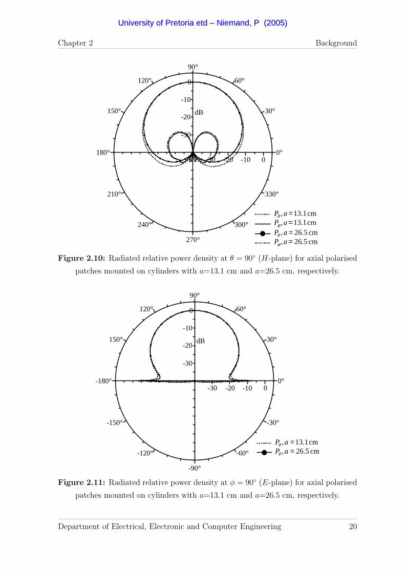
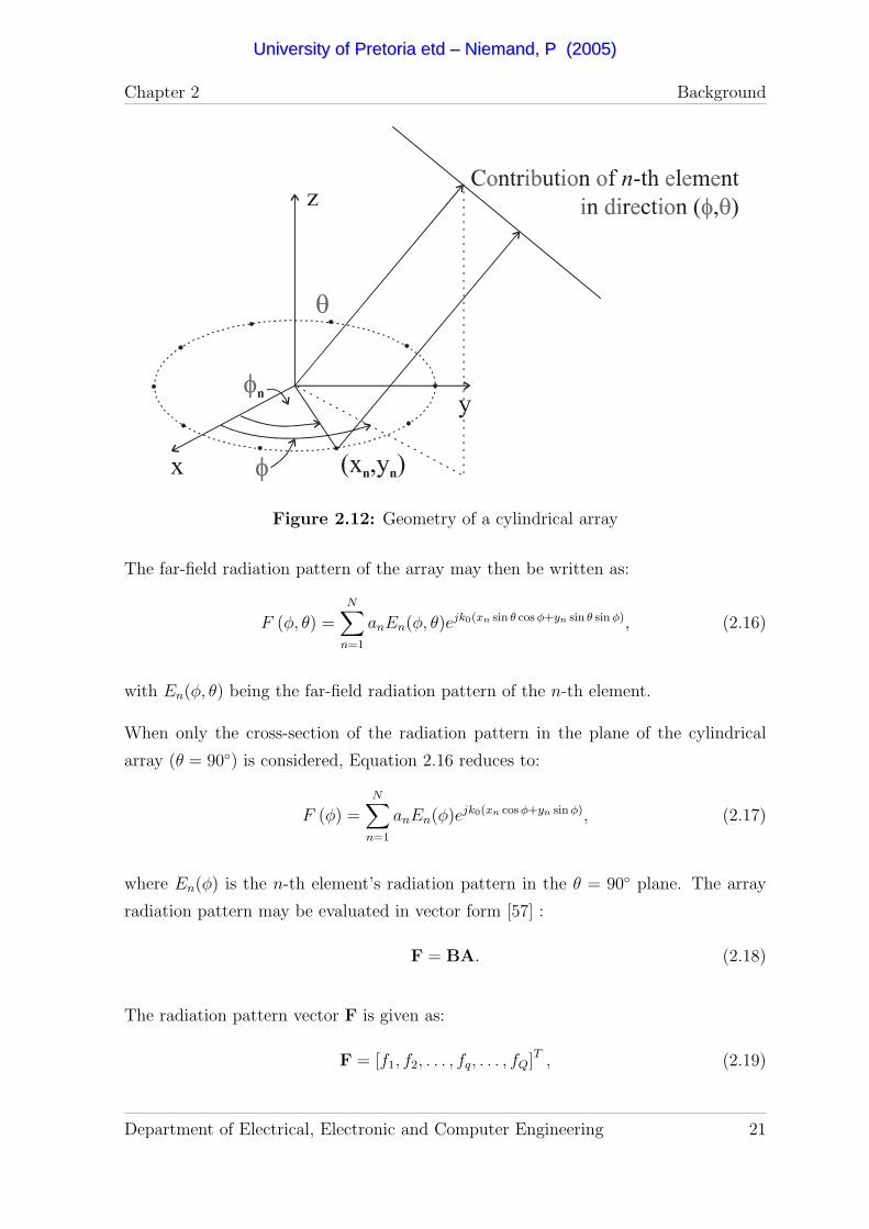
axial polarisation are compared for the two radii in Figures 2.10 and 2.11, respectively.
A small decrease in the back lobe level in the H-plane is observed, while the effect of
the decreased curvature on the main lobe is insignificant in both principle planes. The
cross-polarisation levels for both polarisations appear to be almost unaffected by the
decrease in curvature.
2.2 Cylindrical array pattern
The geometry of a typical cylindrical array can be seen in Figure 2.12. Each array
element is placed on the circumference of the array at (xn, yn), where n = 1 . . . N . The
contribution of the n-th element to the far-field in direction (φ, θ) can be written as:
e (r, φ, θ) = En(r, φ, θ)ejk0(xn sin θ cos φ+yn sin θ sin φ), (2.14)
using the origin of the coordinate system as the reference point. En(r, φ, θ) represent
the co-polarised far-zone electric field of the n-th element with respect to its phase
reference. The radiated electric field of the elements is influenced by the structure on
which it is mounted, e.g. a conducting cylinder or mast, and must therefore be included
when computing element electric fields. The total co-polarised far-zone electric field
ETOT (r, φ, θ) of the array is found by superposition of the element electric fields:
ETOT (r, φ, θ) =N∑
n=1
anEn(r, φ, θ)ejk0(xn sin θ cos φ+yn sin θ sin φ), (2.15)
where an denotes the relative complex excitation (amplitude as well as phase) of the
n-th element.
Department of Electrical, Electronic and Computer Engineering 16
UUnniivveerrssiittyy ooff PPrreettoorriiaa eettdd –– NNiieemmaanndd,, PP ((22000055))
Chapter 2 Background
0°
30°
60°
90°
120°
150°
180°
210°
240°
270°
300°
330°
PP
-10
-20
-10-20
0
-30
-30 0
dB
4.4,1,
==
r
r
PP
εε
φ
φ
Figure 2.4: Radiated relative power density at θ = 90 (E-plane) for circumferentially
polarised patches with εr = 1 and εr = 4.4
-180°
-150°
-120°
-90°
-60°
-30°
0°
30°
60°
90°
120°
150°
PPPP
-10
-20
-10-20
0
-30
-30 0
dB
4.4,4.4,
1,1,
====
r
r
r
r
PPPP
εεεε
φ
θ
φ
θ
Figure 2.5: Radiated relative power density at φ = 90 (H-plane) for circumferentially
polarised patches with εr = 1 and εr = 4.4
Department of Electrical, Electronic and Computer Engineering 17
UUnniivveerrssiittyy ooff PPrreettoorriiaa eettdd –– NNiieemmaanndd,, PP ((22000055))

Chapter 2 Background
0°
30°
60°
90°
120°
150°
180°
210°
240°
270°
300°
330°
PPPP
-10
-20
-10-20
0
-30
-30 0
dB
4.4,4.4,
1,1,
====
r
r
r
r
PPPP
εεεε
φ
θ
φ
θ
Figure 2.6: Radiated relative power density at θ = 90 (H-plane) for axial polarised
patches with εr = 1 and εr = 4.4
-180°
-150°
-120°
-90°
-60°
-30°
0°
30°
60°
90°
120°
150°
PP
-10
-20
-10-20
0
-30
-30 0
dB
4.4,1,
==
r
r
PP
εε
θ
θ
Figure 2.7: Radiated relative power density at φ = 90 (E-plane) for axial polarised
patches with εr = 1 and εr = 4.4
Department of Electrical, Electronic and Computer Engineering 18
UUnniivveerrssiittyy ooff PPrreettoorriiaa eettdd –– NNiieemmaanndd,, PP ((22000055))

Chapter 2 Background
0°
30°
60°
90°
120°
150°
180°
210°
240°
270°
300°
330°
PP
-10
-20
-10-20
0
-30
-30 0
dB
cm 5.26,cm 1.13,
==
aPaP
φ
φ
Figure 2.8: Radiated relative power density at θ = 90 (E-plane) for circumferentially
polarised patches mounted on cylinders with a=13.1 cm and a=26.5 cm, respectively.
-180°
-150°
-120°
-90°
-60°
-30°
0°
30°
60°
90°
120°
150°
PPPP
-10
-20
-10-20
0
-30
-30 0
dB
cm 5.26,cm 5.26,cm 1.13,cm 1.13,
====
aPaPaPaP
φ
θ
φ
θ
Figure 2.9: Radiated relative power density at φ = 90 (H-plane) for circumferentially
polarised patches mounted on cylinders with a=13.1 cm and a=26.5 cm, respectively.
Department of Electrical, Electronic and Computer Engineering 19
UUnniivveerrssiittyy ooff PPrreettoorriiaa eettdd –– NNiieemmaanndd,, PP ((22000055))
Chapter 2 Background
0°
30°
60°
90°
120°
150°
180°
210°
240°
270°
300°
330°
PPPP
-10
-20
-10-20
0
-30
-30 0
dB
cm 5.26,cm 5.26,cm 1.13,cm 1.13,
====
aPaPaPaP
φ
θ
φ
θ
Figure 2.10: Radiated relative power density at θ = 90 (H-plane) for axial polarised
patches mounted on cylinders with a=13.1 cm and a=26.5 cm, respectively.
-180°
-150°
-120°
-90°
-60°
-30°
0°
30°
60°
90°
120°
150°
PP
-10
-20
-10-20
0
-30
-30 0
dB
cm 5.26,cm 1.13,
==
aPaP
θ
θ
Figure 2.11: Radiated relative power density at φ = 90 (E-plane) for axial polarised
patches mounted on cylinders with a=13.1 cm and a=26.5 cm, respectively.
Department of Electrical, Electronic and Computer Engineering 20
UUnniivveerrssiittyy ooff PPrreettoorriiaa eettdd –– NNiieemmaanndd,, PP ((22000055))
Chapter 2 Background
Figure 2.12: Geometry of a cylindrical array
The far-field radiation pattern of the array may then be written as:
F (φ, θ) =N∑
n=1
anEn(φ, θ)ejk0(xn sin θ cos φ+yn sin θ sin φ), (2.16)
with En(φ, θ) being the far-field radiation pattern of the n-th element.
When only the cross-section of the radiation pattern in the plane of the cylindrical
array (θ = 90) is considered, Equation 2.16 reduces to:
F (φ) =N∑
n=1
anEn(φ)ejk0(xn cos φ+yn sin φ), (2.17)
where En(φ) is the n-th element’s radiation pattern in the θ = 90 plane. The array
radiation pattern may be evaluated in vector form [57] :
F = BA. (2.18)
The radiation pattern vector F is given as:
F = [f1, f2, . . . , fq, . . . , fQ]T , (2.19)
Department of Electrical, Electronic and Computer Engineering 21
UUnniivveerrssiittyy ooff PPrreettoorriiaa eettdd –– NNiieemmaanndd,, PP ((22000055))
Chapter 2 Background
where fq is the value of the radiation pattern in the φq-direction for a total number of
Q field points. A is the excitation vector:
A = [a1, a2, . . . , an, . . . , aN ]T , (2.20)
while B is defined as the radiation matrix. The bnq-th element of B is the contribution
of the n-th antenna element to the radiation pattern in the q-th direction:
bnq = anEn(φq)ejk0(xn cos φq+yn sin φq). (2.21)
When all the antenna elements have the same radiation pattern E(φ), polarisation
properties and pointing direction, the array radiation pattern may be written as:
F (φ) = E(φ) ·[
N∑n=1
anejk0(xn cos φ+yn sin φ)
]. (2.22)
From this radiation pattern an array factor can be extracted:
AF (φ) =N∑
n=1
anejk0(xn cos φ+yn sin φ), (2.23)
which is the radiation pattern of an array of isotropic point sources located at the
phase centres of the original elements and with excitations equal to the original element
excitations. Isotropic point sources are fictitious antenna elements that radiate an equal
amount of energy in all directions.
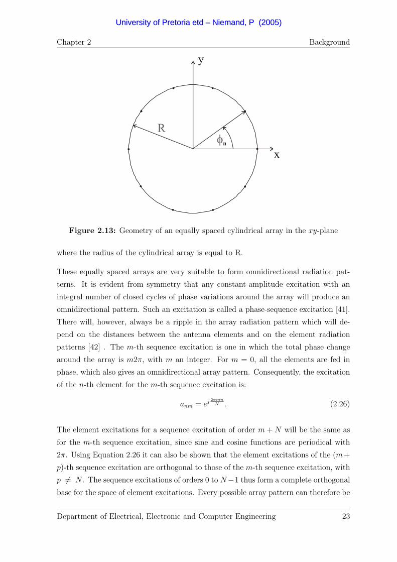
2.2.1 Equally spaced cylindrical arrays
The geometry of an equally spaced cylindrical array in the xy-plane (θ = 90) is shown
in Figure 2.13. The n-th is located at the angle:
φn =2πn
N. (2.24)
The far-field array factor for an equally spaced array with elements identical in radiation
pattern, is given by [41]:
AF (φ) =N∑
n=1
anejk0R cos(φ−φn)
=N∑
n=1
anejk0R cos(φ− 2πnN ),
(2.25)
Department of Electrical, Electronic and Computer Engineering 22
UUnniivveerrssiittyy ooff PPrreettoorriiaa eettdd –– NNiieemmaanndd,, PP ((22000055))
Chapter 2 Background
Figure 2.13: Geometry of an equally spaced cylindrical array in the xy-plane
where the radius of the cylindrical array is equal to R.
These equally spaced arrays are very suitable to form omnidirectional radiation pat-
terns. It is evident from symmetry that any constant-amplitude excitation with an
integral number of closed cycles of phase variations around the array will produce an
omnidirectional pattern. Such an excitation is called a phase-sequence excitation [41].
There will, however, always be a ripple in the array radiation pattern which will de-
pend on the distances between the antenna elements and on the element radiation
patterns [42] . The m-th sequence excitation is one in which the total phase change
around the array is m2π, with m an integer. For m = 0, all the elements are fed in
phase, which also gives an omnidirectional array pattern. Consequently, the excitation
of the n-th element for the m-th sequence excitation is:
anm = ej 2πmnN . (2.26)
The element excitations for a sequence excitation of order m + N will be the same as
for the m-th sequence excitation, since sine and cosine functions are periodical with
2π. Using Equation 2.26 it can also be shown that the element excitations of the (m+
p)-th sequence excitation are orthogonal to those of the m-th sequence excitation, with
p 6= N . The sequence excitations of orders 0 to N−1 thus form a complete orthogonal
base for the space of element excitations. Every possible array pattern can therefore be
Department of Electrical, Electronic and Computer Engineering 23
UUnniivveerrssiittyy ooff PPrreettoorriiaa eettdd –– NNiieemmaanndd,, PP ((22000055))
Chapter 2 Background
realised by the superposition of N sequence excitations. The transformations between
the vectors of element excitations and sequence excitations are given by:
an =N−1∑m=0
smej 2πmnN , (2.27)
and
sm =1
N
N−1∑n=0
ane−j 2πmnN . (2.28)
Equation 2.27 and Equation 2.28 can be seen as a discrete Fourier transform (DFT) and
an inverse discrete Fourier transform (IDFT), respectively. Subsequently, the far-field
array factor of the m-th sequence excitation can be expressed as:
AFm(φ) =N−1∑n=0
smej 2πmnN ejk0R cos(φ− 2πn
N ). (2.29)
Since the element excitations are superpositions of N sequence excitations, the array
factor becomes:
AF (φ) =N−1∑m=0
N−1∑n=0
smej 2πmnN ejk0R cos(φ− 2πn
N ). (2.30)
When the resulting array pattern has a constant amplitude and linear phase, it is called
a phase mode [44]. The order of the phase mode is determined by the number of phase
variations over 2π. A phase mode of order m is:
pm(φ) = ejmφ. (2.31)
The zero order phase mode has constant amplitude and phase, while the negative order
phase modes indicate a reverse variation of phase change with angle. For small inter-
element spacings, the array can be approximated by a continuous source of radiation
and the array factor can then be expressed as [43]:
AF (φ) = N
m=mmax∑m=−mmax
jmsmJm(k0R)ejmφ, (2.32)
where Jm(x) is the Bessel function of the first kind of order m and mmax < N/2. This
array factor is a superposition of N scaled phase modes with −N/2 < m < N/2.
Consequently, a pattern caused by a sequence excitation of order m is a good approx-
imation for a phase mode of the same order if the array radius is small.
Department of Electrical, Electronic and Computer Engineering 24
UUnniivveerrssiittyy ooff PPrreettoorriiaa eettdd –– NNiieemmaanndd,, PP ((22000055))
Chapter 2 Background
2.3 Null synthesis techniques
Various null synthesis techniques for omnidirectional patterns have been presented
[41, 43–55]. These techniques utilise different characteristics of a cylindrical array to
obtain a null at the desired angle location. Some use the sequence excitations, phase
modes or the orthogonal base of realisable array patterns, while others utilise pattern
search techniques. A short overview of these techniques will be given after defining
some null synthesis parameters.
2.3.1 Definitions of parameters in null synthesis
The definitions describing the omnidirectional radiation pattern with a null, differ from
conventional beam forming parameters such as beam width and side lobe levels. Illus-
trations of the definitions used to characterise the null pattern, are given in Figure 2.14.
The gain ripple (in dB) is defined as the ratio between the maximum and minimum
level in the omniregion. The angular distance between the two points, 10 dB below
the maximum, is defined as the null width. The null depth is given by the ratio of
the radiation intensity in the direction of the null and the maximum, which is also an
indication of the suppression level of the interference. For null depths smaller than 10
dB, another appropriate level may be defined at which the null width is measured. The
definition of gain ripple is only valid if the value of the ripple is below this null width
definition level.
2.3.2 Superposition of sequence excitations
The superposition of two sequence excitations to produce a null in an omnidirectional
radiation pattern, was presented by Davies and Rizk [44]. A zero crossing null, where
the radiation pattern show an abrupt phase reversal across the angle position of the
null, was produced. The two phase modes, which had the same amplitude, but were
180 out of phase in the direction of the null, were utilised. The difference in the orders
of the two modes had to be exactly one to avoid any other abrupt phase reversals. The
authors consequently employed the zero and first order sequence excitations. The
Department of Electrical, Electronic and Computer Engineering 25
UUnniivveerrssiittyy ooff PPrreettoorriiaa eettdd –– NNiieemmaanndd,, PP ((22000055))

Chapter 2 Background
-25
-20
-15
-10
-5
0R
adi a
tion
Pat te
rn (
dB)
0 60 120 180 240 300 360Azimuth Angle (degrees)
Null Width
Ripple
Null Depth
Null Position
Figure 2.14: Definitions of parameters used to characterise null forming
excitations of the n-th element was:
an = ej2π nN + Aejφp . (2.33)
The levels of excitation of the two modes were made equal by means of an attenuator
A, and the direction of the null was controlled by a phase shifter φp. Acceptable null
depths are obtainable if the number of elements and the radius of the array is kept
small. If the inter-element spacing is not kept small, the two modes do not exactly
cancel each other. This will lead to finite null depths and errors in the direction of
the null. This technique produced very wide nulls as the amplitude of the radiation
pattern falls monotonically from the maximum towards the null.
As an extension of this technique, the above authors also proposed the superposition
of a third sequence excitation to reduce the null width. A dipole type or figure-of-eight
pattern was superposed to the original pattern. This type of pattern was produced by
the sequence excitations of orders 1 and -1 and has two zero crossing nulls. One of the
two nulls was made to coincide with the original null. The complete excitation vector
Department of Electrical, Electronic and Computer Engineering 26
UUnniivveerrssiittyy ooff PPrreettoorriiaa eettdd –– NNiieemmaanndd,, PP ((22000055))
Chapter 2 Background
was given by:
an = Aejφp + (B + 1)ej2π nN + Be(j2φp−j2π n
N ). (2.34)
The decrease in null width is obtained at the expense of higher gain ripple. The
attenuator B controls the null width, but also has to be fixed at a suitable value to
achieve an acceptable compromise between the null width and gain ripple.
Lim and Davies [41] proposed the use of two phase modes with a higher difference
in order. This would have decreased the null width, but also would have lead to
additional nulls in the radiation pattern. To avoid the additional nulls, the zero order
mode was replaced with a beam pattern, which had a main beam of constant phase
in the direction of the null. The beam pattern with a constant phase beam in the
direction φp was obtained for a cylindrical array of omnidirectional elements by using
the element excitations:
an,beam = e−jk0R cos(φp−2π nN ). (2.35)
A sequence excitation, which was multiplied with a complex factor A, was added to
the excitation of the constant phase beam to obtain a null in the direction φp. The
factor A had to satisfy the following condition:
A · Fm(φp) + Fbeam(φp) = 0, (2.36)
where Fm(φp) was the far-field radiation pattern of the sequence excitation of order m.
The complex factor was found to be:
A = − N
Fm(φp), (2.37)
and the resulting element excitations were:
an = e−jk0R cos(φp−2π nN ) − N
Fm(φp)ej 2πmn
N . (2.38)
The sequence excitation in Equation 2.38 approximates a phase mode of the same
order (m). Theoretically, an infinitely deep null with low gain ripple can be achieved.
The gain ripple is determined by the interference of the phase mode with the sidelobes
of the phase constant beam. The amount of interference is influenced by the number
of elements, the array radius and the order of the phase mode. For a small number of
Department of Electrical, Electronic and Computer Engineering 27
UUnniivveerrssiittyy ooff PPrreettoorriiaa eettdd –– NNiieemmaanndd,, PP ((22000055))

Chapter 2 Background
elements in the array, the order of the phase mode is usually low (zero or one). Larger
arrays require a higher order phase mode to decrease the null width, which may result
in an increased gain ripple. Therefore, the optimal order of the phase mode to be used,
is determined by the radius of the array, the number of elements and the required ripple
and null width.
2.3.3 Fourier approximation of an ideal pattern
The phase modes, which can be approximated by sequence excitations, form an orthog-
onal base for the array factor. A pattern can thus be synthesised by transforming the
desired pattern into a number of phase modes with a Fourier transformation and then
synthesising the phase modes with the sequence excitations. A Fourier transformation
will however result in an infinite number of phase modes, but only the realisable orders
of phase modes may be used to synthesise the pattern (m ≤ N/2).
Lim [43] proposed the approximation of an ideal zero pattern using this method of
approximation. For a minimum null width, an abrupt phase reversal in the pattern
was needed in the direction of the null. To avoid the occurrence of a second null, the
phase in the omniregion also had to change progressively at half the rate of the change
in azimuth angle. An idealised pattern that satisfied these requirements was:
F0(φ) = ej2π−φ+φp
2 ,
φp ≤ φ ≤ φp + 2π.(2.39)
The phase of the pattern changes linearly from 0 (at φ = φp) to π (at φ = φp + 2π)
and has an abrupt phase reversal at φp, as shown in Figure 2.15 for phip = 180.
The approximation of the amplitude pattern of F0(φ) will result in a null of finite
depth, because the realisable pattern is limited in bandwidth and the derivations, with
respect to φ, also have to be smooth. Using the standard method for calculating Fourier
coefficients, the set of phase modes can be determined as:
pm =1
2π
φp+2π∫
φp
F0 (φ) e−jmφdφ
=e−jmφp
π(m− 1
2
) .
(2.40)
Department of Electrical, Electronic and Computer Engineering 28
UUnniivveerrssiittyy ooff PPrreettoorriiaa eettdd –– NNiieemmaanndd,, PP ((22000055))

Chapter 2 Background
0
30
60
90
120
150
180Ph
ase
(deg
rees
)
0 60 120 180 240 300 360Azimuth Angle (degrees)
Figure 2.15: Phase of the idealised null pattern
For cylindrical arrays with identical elements and small inter-element spacings, the
resulting sequence excitations will be:
sm =e−jm(π
2+φp)
πN(m− 1
2
)Jm(k0R)
, (2.41)
where Jm(x) is the Bessel function of the first kind of order m. The element excitations
are obtained from the DFT relation in Equation 2.27.
The Fourier approximation will yield a pattern with a relatively narrow null, but with a
gain ripple of about 2 dB. The realisable null depths are also low when a small number
of elements are used. For small inter-element spacings (< λ0/4) and radii, where the
Bessel function Jm(k0R) is not close to zero, the results appear to be insensitive to the
array radius. For certain array radii, it will not be possible to create all the phase modes
in the far field, if one or more Bessel functions Jm(k0R) are very small or zero [43].
For the sequence excitations, where Jm(k0R) is very small, the phase mode distortions
in the far field pattern of these excitations will be much larger in amplitude than the
wanted phase modes. The corresponding sequence excitations will be very large and
Department of Electrical, Electronic and Computer Engineering 29
UUnniivveerrssiittyy ooff PPrreettoorriiaa eettdd –– NNiieemmaanndd,, PP ((22000055))

Chapter 2 Background
the distortion will dominate the far field, resulting in a large error of the approximation.
Since the approximation is a superposition of phase modes, it will also lead to errors
when the far field patterns, caused by the sequence excitations, are not exactly phase
modes.
2.3.4 Orthogonal projection method
Instead of using the phase modes, the patterns gm, caused by the sequence excitations,
can be used as basis functions. These patterns are also mutually orthogonal and span
the whole space of possible array patterns. Unlike the phase modes in the Fourier
approximation, they can be synthesised exactly. The approximation will thus be better,
especially when using larger inter-element spacings. Vescovo [50] applied this synthesis
procedure to cylindrical arrays to synthesise beam patterns.
Every realisable array pattern, F (φ), of a cylindrical array with equally spaced antenna
elements, can be written as the result of the sequence excitations sm:
F (φ) =N−1∑m=0
smgm(φ), (2.42)
where
gm(φ) =N−1∑n=0
ej2π mnN En(φ). (2.43)
For a cylindrical array of equally spaced elements, the gm(φ) of two different values of
m are orthogonal to each other. A complete orthogonal base for the space of realis-
able array patterns is thus given by gm(φ). For a cylindrical array of omnidirectional
elements gm(φ) is given by:
gm(φ) =N−1∑n=0
ej2π mnN ejk0R cos(φ− 2πn
N ). (2.44)
The unconstrained optimal array pattern Foptim(φ) is the orthogonal projection of the
idealised pattern F0(φ) onto the space of realisable array patterns, when Foptim(φ) gives
the minimum squared distance between F (φ) and F0(φ). The squared distance ρ2(A)
is defined as:
ρ2(A) =
2π∫
0
|F (φ;A)− F0(φ)|2 dφ, (2.45)
Department of Electrical, Electronic and Computer Engineering 30
UUnniivveerrssiittyy ooff PPrreettoorriiaa eettdd –– NNiieemmaanndd,, PP ((22000055))
Chapter 2 Background
where F (φ;A) denotes the array radiation pattern for the excitation vector A. The
unconstrained optimum sequence excitations are thus obtained through the orthogonal
projection [50]:
soptim m =〈F0(φ), gm(φ)〉‖gm(φ)‖2 , (2.46)
with the scalar product given by:
〈f, g〉 =
2π∫
0
f(φ)g(φ)dφ, (2.47)
and the norm obtained from:
‖f‖ =√〈f, f〉. (2.48)
The idealised radiation pattern F0(φ) of [43] in Equation 2.39, may be used in the
projection method to form a null in an otherwise omnidirectional array pattern. This
null synthesis technique was proposed by Abele et al [53, 54]. The pattern F0(φ) is
projected onto the space of realisable array patterns of a cylindrical array of omnidi-
rectional elements, to obtain the sequence excitation. The element excitations are then
obtained through the DFT relation.
When the inter-element spacing is small (¿ λ0/2), the base functions gm(φ) are good
approximations of the phase modes of the pattern and consequently the results of the
projection method and the Fourier approximation will be comparable. The projection
method also takes into account the distortion of the phase modes and will therefore
give better results than the Fourier approximation for larger inter-element spacings.
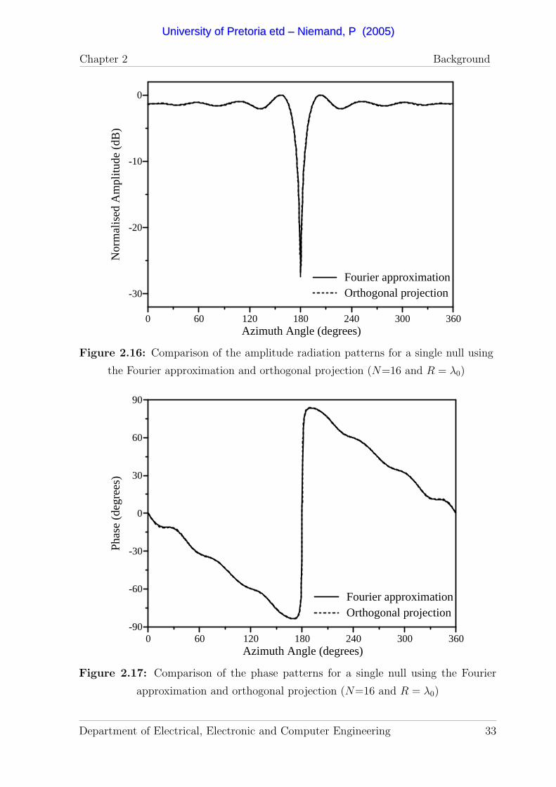
Figures 2.16 and 2.17 respectively compare the amplitude and phase of the radiation
patterns for a single null, using the Fourier approximation and orthogonal projection
method. An array with 16 elements and a radius of λ0 was used to form an infinitely
deep null at 180. Using this small inter-element spacing, the two methods yield similar
results in both amplitude and phase. The amplitude and phase of the radiation patterns
for the same null, using a larger inter-element spacing (R = 1.385λ0), are shown in
Figures 2.18 and 2.19, respectively. For this larger inter-element spacing, the orthogonal
projection method produces a deeper null with less gain ripple. A smaller phase ripple
is also observed in the phase pattern of the orthogonal projection method.
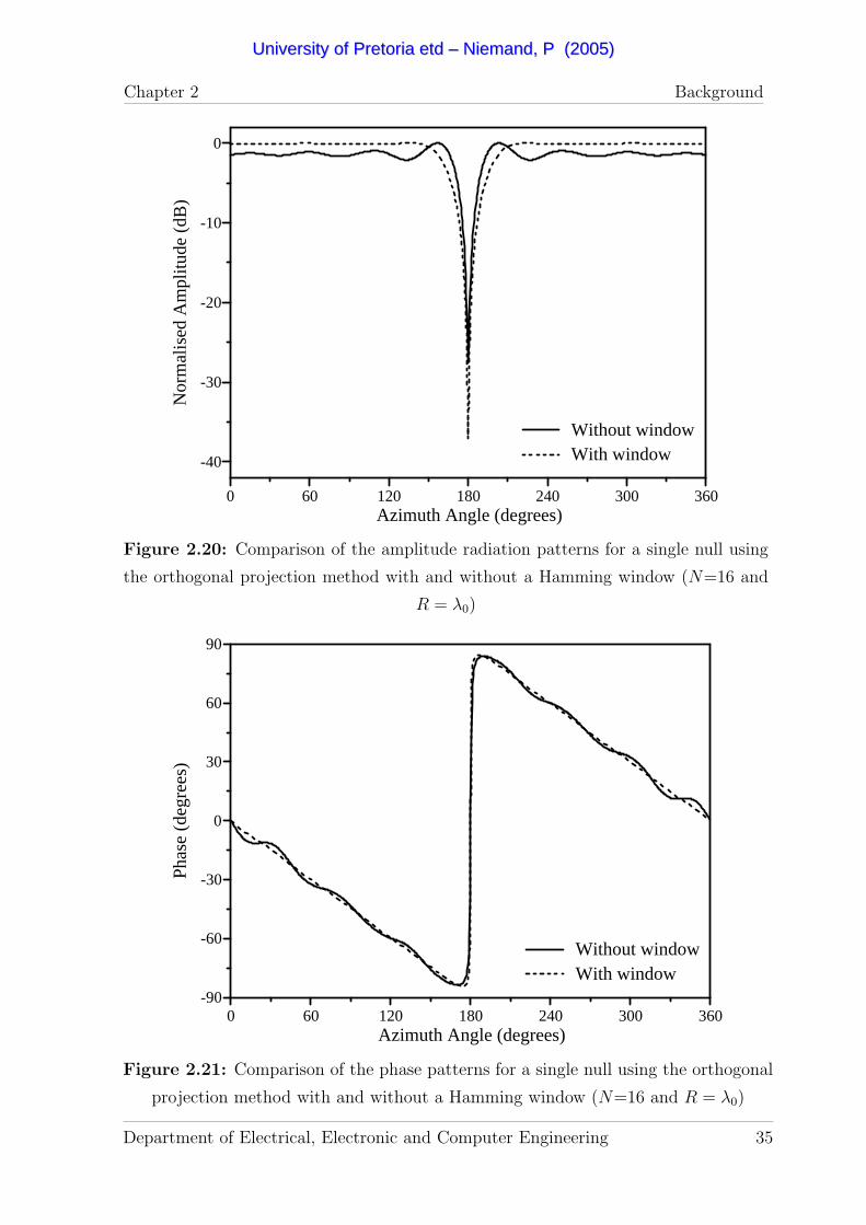
The gain ripple may be reduced by using window functions [53, 54]. The spectral
components of the array pattern, which have to be multiplied with the window function,
Department of Electrical, Electronic and Computer Engineering 31
UUnniivveerrssiittyy ooff PPrreettoorriiaa eettdd –– NNiieemmaanndd,, PP ((22000055))

Chapter 2 Background
are the phase modes. Since the sequence excitations and phase modes are related
through a multiplication of a constant factor, the window function may be applied to
the sequence excitations, instead of the phase modes.
Abele [54] proposed the application of a Hamming window of length N to the sequence
excitations:
WHM(k) = 0.54 + 0.46cos
(2π
k
N
). (2.49)
The idealised pattern has a constant phase slope of a 12
and therefore its Fourier compo-
nents are symmetric to k = 12. This symmetry may not be disturbed by the application
of the window in order to maintain the linear phase change. The best results are thus
obtained if the window is shifted and the m-th sequence excitation coefficient is mul-
tiplied by W (m− 12). The window function may be applied to the sequence excitation
coefficients of both the Fourier approximation and the orthogonal projection. The rip-
ple is decreased using the window function, while the null width is increased. The null
depth may also be significantly increased. As an example, an array with N = 16 and
R = λ0 was used to form a single null at 180. The effects of the Hamming window
on the amplitude and phase of the radiation patterns resulting from the orthogonal
projection method, are shown in Figures 2.20 and 2.21, respectively. It is observed
that although a deeper null with less ripple is formed, the null width is increased.
The idealised pattern can be extended to contain multiple phase reversals to achieve
more than one null in an otherwise omnidirectional pattern. Abele proposed idealised
patterns for an odd and even numbers of nulls. The phase reversals for an even number
of nulls sum up to a total phase change of zero, while the phase reversals for an odd
number of nulls give an overall phase change of ±180. Hence, a linear phase change
has to be introduced to a pattern with an odd number of nulls, while no phase is needed
for an even number of nulls.
The null widths of the multiple nulls do not differ much from the null width of a single
null if the angular spacing between the nulls are kept large enough. On the other hand,
the ripple changes significantly as the ripple caused by the abrupt phase reversals are
superimposed. The angular distances between the nulls determine if there will be an
increase or decrease in the ripple between the nulls. The angular distance between two
nulls may not be too small, otherwise one null will be formed between the nulls.
Department of Electrical, Electronic and Computer Engineering 32
UUnniivveerrssiittyy ooff PPrreettoorriiaa eettdd –– NNiieemmaanndd,, PP ((22000055))
Chapter 2 Background
-30
-20
-10
0
Nor
mal
ised
Am
plitu
de (
d B)
0 60 120 180 240 300 360Azimuth Angle (degrees)
Fourier approximationOrthogonal projection
Figure 2.16: Comparison of the amplitude radiation patterns for a single null using
the Fourier approximation and orthogonal projection (N=16 and R = λ0)
-90
-60
-30
0
30
60
90
P has
e (d
e gre
es)
0 60 120 180 240 300 360Azimuth Angle (degrees)
Fourier approximationOrthogonal projection
Figure 2.17: Comparison of the phase patterns for a single null using the Fourier
approximation and orthogonal projection (N=16 and R = λ0)
Department of Electrical, Electronic and Computer Engineering 33
UUnniivveerrssiittyy ooff PPrreettoorriiaa eettdd –– NNiieemmaanndd,, PP ((22000055))

Chapter 2 Background
-30
-20
-10
0
Nor
mal
ised
Am
plitu
de (
d B)
0 60 120 180 240 300 360Azimuth Angle (degrees)
Fourier approximationOrthogonal projection
Figure 2.18: Comparison of the amplitude radiation patterns for a single null using
the Fourier approximation and orthogonal projection (N=16 and R = 1.385λ0)
-90
-60
-30
0
30
60
90
P has
e (d
e gre
es)
0 60 120 180 240 300 360Azimuth Angle (degrees)
Fourier approximationOrthogonal projection
Figure 2.19: Comparison of the phase patterns for a single null using the Fourier
approximation and orthogonal projection (N=16 and R = 1.385λ0)
Department of Electrical, Electronic and Computer Engineering 34
UUnniivveerrssiittyy ooff PPrreettoorriiaa eettdd –– NNiieemmaanndd,, PP ((22000055))
Chapter 2 Background
-40
-30
-20
-10
0
Nor
mal
ised
Am
plitu
de (
d B)
0 60 120 180 240 300 360Azimuth Angle (degrees)
Without windowWith window
Figure 2.20: Comparison of the amplitude radiation patterns for a single null using
the orthogonal projection method with and without a Hamming window (N=16 and
R = λ0)
-90
-60
-30
0
30
60
90
P has
e (d
e gre
es)
0 60 120 180 240 300 360Azimuth Angle (degrees)
Without windowWith window
Figure 2.21: Comparison of the phase patterns for a single null using the orthogonal
projection method with and without a Hamming window (N=16 and R = λ0)
Department of Electrical, Electronic and Computer Engineering 35
UUnniivveerrssiittyy ooff PPrreettoorriiaa eettdd –– NNiieemmaanndd,, PP ((22000055))
Chapter 2 Background
An omnidirectional pattern with two nulls at 90 and 270, respectively, were simulated
using the orthogonal projection method with a Hamming window. Figures 2.22 and
2.23 show the resulting amplitude and phase of the radiation pattern, respectively. An
additional null was introduced at 180 and the amplitude and phase of the radiation
pattern with three nulls are shown in Figures 2.24 and 2.25.
The difference in the phase patterns for odd and even nulls can be seen when Fig-
ures 2.23 and 2.25 are compared. A linear phase change is required for the introduction
of the three nulls, whereas introduction of two nulls require no phase change. When
comparing Figures 2.22 and 2.24, the effect of the spacing between the nulls on the
null depths can also be seen. The null depths changed as the null spacing decreased
from 180 to 90.
Phase reversals of±180 do not guarantee infinitely deep nulls. In general, the depths of
the realised nulls depend on the array radius, the number of elements and the angular
distance between the nulls. Abele [54] proposed the use of a variable phase step to
provide control over the realised null depth. For a phase step of angle α, the absolute
value of the average of both sides of the step will be:
∣∣∣F∣∣∣ =
|1 + ejα|2
= cosα
2.
(2.50)
If the desired null depth is expressed in dB relative to the maximum of the pattern,
the required phase difference to achieve this null depth will be:
α = 2arccos(10FdB/20
). (2.51)
The overall phase slope for a single null has to be α/2π to keep the pattern smooth in
the omni-region. To introduce multiple nulls with specified null depths in the idealised
pattern, the overall phase difference, after introducing the appropriate phase steps, has
to be cancelled by a linear phase change. Therefore, the required phase slope of the
idealised pattern for a number (L) of step angles αl will be:
ν = − 1
2π
L∑
l=1
∆lαl, (2.52)
where ∆l is the step direction of the phase step which may be equal to -1 or 1.
Department of Electrical, Electronic and Computer Engineering 36
UUnniivveerrssiittyy ooff PPrreettoorriiaa eettdd –– NNiieemmaanndd,, PP ((22000055))

Chapter 2 Background
-40
-30
-20
-10
0
Nor
mal
ised
Am
plitu
de (
d B)
0 60 120 180 240 300 360Azimuth Angle (degrees)
Figure 2.22: Amplitude radiation pattern for two nulls using the orthogonal projec-
tion method with a Hamming window (N=16 and R = λ0)
0
60
120
180
Phas
e (d
egre
es)
0 60 120 180 240 300 360Azimuth Angle (degrees)
Figure 2.23: Phase pattern for two nulls using the orthogonal projection method with
a Hamming window (N=16 and R = λ0)
Department of Electrical, Electronic and Computer Engineering 37
UUnniivveerrssiittyy ooff PPrreettoorriiaa eettdd –– NNiieemmaanndd,, PP ((22000055))

Chapter 2 Background
-40
-30
-20
-10
0
Nor
mal
ised
Am
plitu
de (
d B)
0 60 120 180 240 300 360Azimuth Angle (degrees)
Figure 2.24: Amplitude radiation pattern for three nulls using the orthogonal pro-
jection method with a Hamming window (N=16 and R = λ0)
-120
-60
0
60
120
Phas
e (d
egre
es)
0 60 120 180 240 300 360Azimuth Angle (degrees)
Figure 2.25: Phase pattern for three nulls using the orthogonal projection method
with a Hamming window (N=16 and R = λ0)
Department of Electrical, Electronic and Computer Engineering 38
UUnniivveerrssiittyy ooff PPrreettoorriiaa eettdd –– NNiieemmaanndd,, PP ((22000055))

Chapter 2 Background
The directions of the phase steps are chosen in such a way as to minimise the sum
of the phase differences and consequently minimise the required phase slope. If the
previously mentioned windowing is required, the window displacement must be equal
to ν. This method provides control over the null depths with acceptable accuracy,
if the null depths are kept below 20 dB. Again the accuracy depends on the array
configuration as well as the angular spacing between the nulls. The specified angular
position of a null also has an influence on the null depth accuracy.
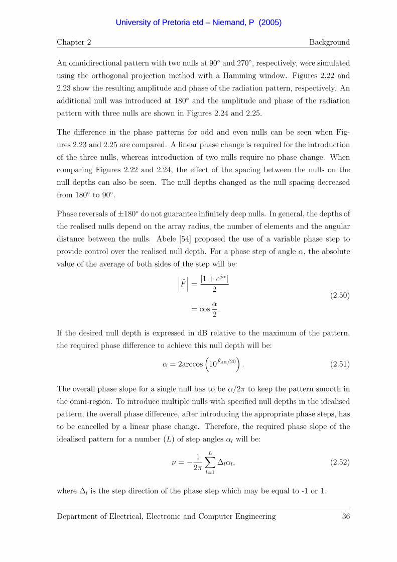
As an example, three nulls of depths 10 dB, 15 dB and 25 dB were required at 60,
180 and 270, respectively. The orthogonal projection, with a Hamming window, was
utilised to form the desired nulls in the omnidirectional pattern of a 16 element array
with a radius of λ0. Figures 2.26 and 2.27 show the resulting amplitude and phase
of the realised radiation pattern. The realised null depths are 9.9 dB, 15.1 dB and
24.1 dB at 60, 180 and 270, respectively. Each null depth requires a different phase
step, as seen in the phase pattern in Figure 2.27. As the required null depth decreases,
the null is also broadened.
2.3.5 Pattern synthesis with null constraints
When the radiation pattern is already given, Vescovo [50,51,55] proposed a method to
introduce nulls into the pattern subsequently. The method was applied to reduce the
sidelobe level by forming additional nulls near the main beam in a conventional beam
pattern.
A radiation pattern, which does not necessarily satisfy the null constraint, is given by
the N excitations a0n. The L null constraints, at the angles φl, are given by F (φl) = 0
for l = 1 . . . L− 1.
The N excitations that minimise the Euclidean distance between the radiation pattern
of a0n and the pattern that satisfies the null constraint, are defined as a′n. The squared
Euclidean distance between the two patterns given by the sequence excitations s0m and
s′m, is defined as:
η2 =N−1∑
k=0
∣∣b0m − b′m
∣∣2
=∥∥b0 − b′
∥∥2,
(2.53)
Department of Electrical, Electronic and Computer Engineering 39
UUnniivveerrssiittyy ooff PPrreettoorriiaa eettdd –– NNiieemmaanndd,, PP ((22000055))
Chapter 2 Background
-25
-20
-15
-10
-5
0
Nor
mal
ised
Am
plitu
de (
d B)
0 60 120 180 240 300 360Azimuth Angle (degrees)
Figure 2.26: Amplitude radiation pattern of three nulls of required depths 10 dB,
15 dB and 25 dB at 60,180 and 270, respectively. (N=16 and R = λ0)
-180
-120
-60
0
60
120
180
Phas
e (d
egre
es)
0 60 120 180 240 300 360Azimuth Angle (degrees)
Figure 2.27: Phase pattern for three nulls of required depths 10 dB, 15 dB and 25 dB
at 60,180 and 270, respectively. (N=16 and R = λ0)
Department of Electrical, Electronic and Computer Engineering 40
UUnniivveerrssiittyy ooff PPrreettoorriiaa eettdd –– NNiieemmaanndd,, PP ((22000055))
Chapter 2 Background
where
b0m = ‖gm‖s0
m (2.54)
and
b′m = ‖gm‖s′m. (2.55)
Subsequently, the null constraints can be expressed as Bb′ = 0, where B = [Blm] and
Blm = gm(φl)/‖gm‖ for l = 0 . . . L− 1 and m = 0 . . . N − 1. The problem can therefore
be described as minimising the Euclidian distance ‖b0 − b′‖2 under the constraint
Bb′ = 0. The optimal vector b′ is given by [51]:
b′ = [IN −BH(BBH)−1B]b0, (2.56)
where IN is a N ×N identity matrix and BH denotes the complex conjugate transpose
of B.
To obtain an omnidirectional pattern with nulls, the excitation vector a0 must be
chosen in such a way as to yield an acceptable a′. For the lowest possible ripple, a0
will be an excitation vector, which results in an omnidirectional pattern. The method
produces infinitely deep nulls exactly at the desired angles, but with a gain ripple which
can be as high as 20 dB.
Vescovo also proposed this technique to introduce nulls in the desired pattern of an arc
array of directional elements [56]. Each directional element had a theoretical radiation
pattern of:
En(φ) = 1 + cos(φ− φn). (2.57)
Since the element radiation patterns point in different directions, the element pattern
can not be factorised out of the array pattern to obtain an array factor [4,57]. Therefore,
the orthogonal base defined in Equation 2.43 is used to obtain the desired pattern
through the projection method. Additional nulls are formed afterwards by using null
constraints.
2.3.6 Constrained minimisation with Lagrange multipliers
In this method, the distance between an idealised pattern and the realised pattern is
also minimised [47]. As opposed to other methods, the idealised pattern has a constant
phase and therefore the phase of the realised pattern will be almost constant. This
Department of Electrical, Electronic and Computer Engineering 41
UUnniivveerrssiittyy ooff PPrreettoorriiaa eettdd –– NNiieemmaanndd,, PP ((22000055))

Chapter 2 Background
will result in an tangential null, where the phase is constant within the null and the
resulting null width will consequently not be optimal. The squared error function:
ε2 =
π∫
−π
|AF (φ)− 1| dφ, (2.58)
is minimised, subject to AF (φp) = 0, where φp is the angle position of the null. The
squared error is minimised using the method of Lagrange multipliers, which result in
the vector of element excitations:
a = Q−1
[p− dH(φp)Q
−1p
d(φp)Q−1d(φp)d(φp)
], (2.59)
where Q is an N ×N matrix with elements:
Qij = J0
(2k0Rsin
( π
N|i− j|
)). (2.60)
The N -dimensional vectors d(φ) and p have elements:
di(φ) = ejk0Rcos(φ− 2πN ), (2.61)
and
pi(φ) = J0(k0R), (2.62)
respectively.
The realised pattern of this method has an infinitely deep null exactly at the desired
location of the null. The tangential null is wider than the zero-crossing null and show
a gain ripple between 2.5 and 3.5 dB. The constant idealised phase appears not to be
suitable for the synthesis of an omnidirectional pattern with a narrow null and low gain
ripple.
2.3.7 Constrained optimisation techniques
The methods, which have been discussed in the previous sections, all provide an om-
nidirectional pattern with nulls, but with different null depths, null widths and gain
ripples. These methods do not have the ability to constrain a certain property of the
array pattern.
Department of Electrical, Electronic and Computer Engineering 42
UUnniivveerrssiittyy ooff PPrreettoorriiaa eettdd –– NNiieemmaanndd,, PP ((22000055))
Chapter 2 Background
Constrained optimisation allows the prescription of some of the characteristics of the
array pattern, while optimising the others. The null width, for example, may be
optimised for a given gain ripple and null depth, or the gain ripple may be minimised,
while specifying the null width and null depth values. An optimisation technique
may also allow the definition of any criteria relevant to the specified application e.g.
allowable excitation amplitudes and phases.
These optimisation techniques may utilise methods such as the least squares optimisa-
tion method [45], the minimax and linear programming methods [48], the Hooke and
Jeeves algorithm [45] and the simulated annealing method [52]. Prasad [45] applied the
least squares optimisation method to circular and arc arrays to form a beam pattern
with a specified beamwidth. Additional nulls were also placed in the sidelobe region by
using null constraints while minimising the mean square difference between the desired
pattern and the optimum pattern. The Hook and Jeeves algorithm was also used to
perform an iterative search to find the optimum excitation vector while satisfying the
null constraints. During the search, the sidelobe level was minimised.
For linear arrays, Mismar [48] introduced a method to locate nulls in the prescribed
directions while keeping the main beam towards the desired signal. A minimax approx-
imation technique is used to search for the maximum point in the constraint region
to control the sidelobe level directly, while at the same time control the main beam
characteristics as required. Ares et al. [52] used a simulated annealing technique to
produce beam patterns for a circular arc array on a cylinder. A cost function, which
could include terms to control the radiation pattern, was minimised. Terms which
placed constraints on the excitations, could also be included in the cost function.
Since the desired pattern is a function of the excitation vector, the search is executed
in a 2N -dimensional space. A high computational expense is thus encountered. The
choice of the starting values also plays a very important roll in the success of these
pattern search techniques. Choosing the starting values carefully can limit the compu-
tational time and avoid local minima. The use of an excitation vector, with a resulting
pattern error close to the global minimum, is encouraged.
Department of Electrical, Electronic and Computer Engineering 43
UUnniivveerrssiittyy ooff PPrreettoorriiaa eettdd –– NNiieemmaanndd,, PP ((22000055))

Chapter 2 Background
2.4 Mutual coupling compensation
If the element excitations, obtained from the null synthesis technique, are applied to
the antenna elements, distortion of these excitations may occur due to the mutual
coupling between the antenna elements in the array. The consequent errors in the
element excitations deteriorate the desired radiation pattern [72, 73]. Therefore, the
mutual coupling must be compensated for to avoid errors in the desired characteristics
of the null.
Lo [74] investigated the effect of the mutual coupling on the beam scanning and null
steering performance of a linear monopole array. It was found that null filling and/or
null steering errors occurred when the mutual coupling was not compensated for during
the computation of the element excitations. The effect of the mutual coupling on the
null pattern of a cylindrical dipole array was studied by Abele et al. [54]. The mutual
coupling between the dipoles had a deforming effect on the the null pattern. Null filling
and null position errors also occurred and the gain ripple was increased.
One direct way of minimising the effect of the mutual coupling, is by reducing the
mutual coupling itself. The antenna elements in the array, for example, can be designed
in such a way as to exhibit small coupling values. Absorbing material can be placed
between the elements to reduce the coupling or the spacing between the elements can
be chosen in such a way, that the coupling has an insignificant effect on the desired
radiation pattern.
Another way of dealing with the coupling, is to compensate for it in the pattern syn-
thesis technique. Impedance and coupling matrixes are used in the pattern synthesis
technique to compute corrected element excitations, which compensate for the mutual
coupling. According to Ghorbani [87], the mutual coupling also causes a mismatch
between the driving impedances of the antenna elements and the feeding system of the
array. This effect may significantly degrade the performance of narrowband arrays.
These driving impedances can be corrected by altering the physical properties of the
antenna elements to obtain the desired driving impedances for a required set of element
excitations. A short overview of these techniques is given in the following sections.
Department of Electrical, Electronic and Computer Engineering 44
UUnniivveerrssiittyy ooff PPrreettoorriiaa eettdd –– NNiieemmaanndd,, PP ((22000055))
Chapter 2 Background
2.4.1 Minimising the mutual coupling effects
Lo and Vu [74] investigated the use of guard elements in a linear monopole array to
reduce the effect of the mutual coupling on null steering. Due to mutual coupling, the
active element patterns are not comparable, which result in null filling and null steering
errors. It was found that by placing guard elements at both ends of the linear array,
the active element patterns resemble each other more closely. The perturbation of the
zeros is reduced and consequently the null filling and null steering error are minimised.
The method does not completely compensate for the mutual coupling, but is able to
minimise the coupling effect without changing the element excitations.
When computing the coupling between array elements, the coupling of the electro-
magnetic fields in the free space immediately above the elements, is usually considered
in the calculation. For microstrip array elements constructed on the same common
substrate, additional coupling occurs due to the surface wave in the substrate. When
using thick substrates, this surface wave coupling can be very strong due to a larger
surface wave being generated. Bamford et al [81] examined the direct radiation and
surface wave coupling separately through a method based on the reaction theorem.
The behaviour of the total coupling was also studied for various element separation
distances and substrate thicknesses. It was found that when the two coupling parame-
ters are in phase, they add to form an upper limit curve for the coupling, but also form
a lower limit curve when they are opposite in phase. A reduction in mutual coupling
is thus possible through an appropriate choice of substrate thickness and separation
distance between the array elements. The possible heights for the substrate are usually
determined by the required bandwidth and the available substrate thicknesses as sup-
plied by the manufacturers. Similarly, the possible separation distances are limited by
the desired radiation pattern characteristics. Therefore, the reduction of the mutual
coupling using this method may be limited by the requirements on the impedance and
radiation behaviour of the array.
2.4.2 Compensation using coupling and impedance matrixes
Steyskal and Herd [76] showed that the element excitations an can always be chosen
in such a way as to compensate for the pattern error due to mutual coupling. The
technique uses the formulation that any composite array pattern is a weighted sum
Department of Electrical, Electronic and Computer Engineering 45
UUnniivveerrssiittyy ooff PPrreettoorriiaa eettdd –– NNiieemmaanndd,, PP ((22000055))
Chapter 2 Background
of the isolated element patterns and that the mutual coupling parasitically excites all
the elements. The mutual coupling can thus be compensated for by driving the array
with modified element excitations in such a way that the desired radiation pattern is
obtained in the presence of these parasitics. The coupling perturbed signals and the
unperturbed desired signals, can be related through a coupling matrix C:
v = Cvd, (2.63)
where the vectors v and vd represent the coupling perturbed signals vn and the desired
signals vdn, respectively. The compensation for the mutual coupling can thus be accom-
plished by simply multiplying the received signals v with the inverse of the coupling
matrix:
vd = C−1v. (2.64)
This method restores the signals as being received by the isolated antenna elements
in the absence of coupling. The coupling coefficients can be obtained from two differ-
ent methods: a Fourier decomposition of the measured element patterns or coupling
measurements between the array ports. The matrix C−1 may be very difficult or im-
practical to realise with an analog network, but can be easily realised in a digital beam
forming antenna system. Darwood et al also extended this technique for planar ar-
rays [82]. The method assumes that the current distribution over the array elements
is not affected by the coupling and remains unchanged from one element to the other
in the array. It is furthermore assumed that only the input impedance of the element
is affected by the mutual coupling. This approach may fail when electrically large
elements and arrays of dissimilar elements are considered.
Any errors in the coupling matrix, due to these assumptions, will contribute to the
degradation of difference beam patterns. Fletcher et al [80] derived a covariance ma-
trix for any signal direction of arrival that includes the effects of the mutual coupling.
By multiplying the inverse of this covariance matrix with the coupling corrected dif-
ference beam excitation vector, an optimum excitation vector is found which restores
the difference beam pattern.
Derneryd [79] proposed an alternative way of viewing the matrix multiplication tech-
nique. An array antenna can be represented by a multiport network that is charac-
terised by a N×N scattering matrix, S [75]. This scattering matrix relates the forward
Department of Electrical, Electronic and Computer Engineering 46
UUnniivveerrssiittyy ooff PPrreettoorriiaa eettdd –– NNiieemmaanndd,, PP ((22000055))

Chapter 2 Background
and backward travelling waves, v+ and v−, respectively, on the feed lines:
v− = Sv+. (2.65)
The array excitation vector A is given by the sum of the incident and reflected signals
and in the transmitting mode it becomes:
A = v+ + v−
= (I + S)v+
= Cv+,
(2.66)
where I is the unit matrix. The modified incident signals to produce the desired
radiation pattern in the mutually coupled environment, is thus given by:
v+ = C−1vd. (2.67)
These modified signals can be controlled by amplifiers and phase shifters.
The inclusion of the mutual coupling in the relation of the incident and reflected waves
is also applied by Eclercy et al [72,77], though in this method the effect of the mutual
coupling is taken into account in the radiated field of the array. The reflection coefficient
at the feed line of the n-th antenna element is defined as:
Γn =v−nv+
n
, (2.68)
where
v−n =N∑
p=1
Snpv+p . (2.69)
Keeping the mutual coupling in mind, the radiation pattern can be written as:
F (φ) =N∑
n=1
En(φ)(v+n + v−n )ejk0(xn cos φ+yn sin φ)
=N∑
n=1
En(φ)v+n (1 + Γn)ejk0(xn cos φ+yn sin φ).
(2.70)
Department of Electrical, Electronic and Computer Engineering 47
UUnniivveerrssiittyy ooff PPrreettoorriiaa eettdd –– NNiieemmaanndd,, PP ((22000055))
Chapter 2 Background
This radiation pattern is then used in the pattern synthesis method to obtain the
modified element excitations, which compensate for the mutual coupling.
Using the vector notation of Equation 2.18, the array radiation pattern can be written
as [83]:
F = B(I + S)v+
= B′v+,
(2.71)
where A is replaced using Equation 2.66. The matrix B′ and the pattern F are com-
puted at more angles than there are elements in the array. The solution for v+ is thus
obtained in a least squares sense. This method assumes that the element patterns are
all equal to the element pattern of an isolated element. Where antenna elements are
closely spaced, the current distributions of the elements are changed by the coupling,
resulting in active element patterns. Taking this into consideration, Caccavale et al [85]
proposed an active element convex programming method (ACE-COP), in which the
array radiation pattern is expressed as the superposition of active element patterns.
The method is mostly applicable to small arrays, due to the additional computational
burden required by the evaluation of the active element patterns. In large arrays,
where most of the elements experience similar electromagnetic environments, it can be
assumed that all the elements radiate the same active element pattern. This approach
is referred to as the modified element pattern (m.e.p.) technique [85].
The correction for the mutual coupling may also be done through the impedance [54,
78,85] or admittance [84] relations between the antenna element currents and voltages.
If the currents of the antenna elements are set proportional to the computed excitation
coefficients, the driving voltages of the elements can be expressed as:
V = ZI, (2.72)
with V and I being 1 × N the driving voltage and current vectors, respectively, and
Z being a N × N impedance matrix. The driving voltage of the m-th element, that
compensates for the mutual coupling with the other antenna elements, can thus be
Department of Electrical, Electronic and Computer Engineering 48
UUnniivveerrssiittyy ooff PPrreettoorriiaa eettdd –– NNiieemmaanndd,, PP ((22000055))
Chapter 2 Background
written as:
Vm =N∑
n=1
ZmnIn
= ZsmmIm +
N∑n=1n6=m
ZmnIn,
(2.73)
where Zsmm is the self impedance of the m-th antenna element and Zmn is the mu-
tual impedance between the m-th and n-th antenna elements. The self and mutual
impedances depend on the type of antenna elements as well as the mounting structure
used to construct the array. Abele et al [54] introduced a variable:
Zn =
Zsnn for n mod N = 0,
Z1,n mod N for n mod N 6= 0,(2.74)
for n = 1 . . . N . Equation 2.73 can then be written as:
Vm =N∑
n=1
Zm−nIn
= Zn; n = 1 . . . N ∗ In; n = 1 . . . N,
(2.75)
where the asterisk denotes a circular convolution.
The correction for the mutual coupling can be included in the design procedure by
multiplying the desired sequence excitation coefficients with the DFT of the impedances
Zn, before computing the element excitations an. The element currents and driving
voltages are then defined as:
In = I0 · IDFTsm; m = 1 . . . N, (2.76)
and
Vn = I0 · IDFT(DFTZn; n = 1 . . . N · sm; m = 1 . . . N). (2.77)
When setting the element voltages proportional to the excitation coefficient, similar
expressions can be found for the necessary driving currents, using the admittance
relation:
I = YV. (2.78)
Department of Electrical, Electronic and Computer Engineering 49
UUnniivveerrssiittyy ooff PPrreettoorriiaa eettdd –– NNiieemmaanndd,, PP ((22000055))

Chapter 2 Background
The driving current of the m-th element may also be written as:
Im =N∑
n=1
YmnVn
= Y smmVm +
N∑n=1n6=m
YmnVn,
(2.79)
with Y smm and Ymn respectively denoting the self admittance of the m-th element and
mutual admittance between the m-th and n-th elements.
2.4.3 Modification of the driving impedances
From Equation 2.73, the driving impedance of the m-th element can be expressed as:
Zam = Zs
mm +N∑
n=1n6=m
ZmnIn
Im
. (2.80)
It is observed that the driving impedances do not only depend on the configurations
of the array and the antenna elements, but also on the currents of the elements. When
designing the feed network of the array, it is these driving impedances which have to
be matched. If the mismatches at the feed ports are not taken into account, it may
significantly degrade the performance of narrowband arrays. The resulting driving
impedances obtained from the radiation pattern correction methods remain unmatched
and unequal. Consequently, the design of a feeding and matching network can be
complicated.
Another possibility is to alter the individual element geometries physically in order to
have equal driving impedances for the required element excitations [86, 88, 89]. Yang
et al [86] proposed this technique for an electromagnetically coupled (EMC) dipole
antenna array. From Equation 2.79, the driving admittance of each element in the
array can be obtained as:
Y am = Y s
mm +N∑
n=1n6=m
YmnVn
Vm
. (2.81)
Department of Electrical, Electronic and Computer Engineering 50
UUnniivveerrssiittyy ooff PPrreettoorriiaa eettdd –– NNiieemmaanndd,, PP ((22000055))
Chapter 2 Background
In a linear system, a second design equation can be derived from the current in each
dipole:
Iam
Vm
=Imm
Vm
+N∑
n=1n6=m
Imn
Vn
, (2.82)
where Imm is the current of the m-th dipole in the absence of other dipole and Imn is
the current of the m-th dipole due to the current on the n-th dipole. The admittances
and currents are functions of the voltages, dipole lengths and dipole offsets from the
microstrip feed line. For a given design goal, e.g. the active currents on the dipoles,
a set of dipole lengths and offsets is found, which not only satisfies Equation 2.82,
but also provides the prescribed driving admittances seen by the feed lines. Design
curves for the mutual admittances and self admittances are obtained from a method
of moments solution. A desired bandwidth and voltage standing wave ratio (VSWR)
at the resonant frequency are obtainable, while finding good agreement between the
desired and measured radiation patterns.
Chen et al proposed a similar technique for a linear array of parallel dipoles [88]. In
this case, the lengths and the radii of the dipoles were changed to obtain the desired
radiation pattern as well as equal driving impedances for the dipoles. This resulted in
a feed network that was much simpler than usual. The technique was also extended
to planar dipole arrays [89]. Input impedances of 75Ω for the dipoles, as well as the
required radiation pattern, were obtained.
2.5 Summary
Different characteristics of the cylindrical microstrip patch antenna have been dis-
cussed. The cavity model was used to illustrate the influence of some of the design
parameters of the cylinder and the patch antenna on the radiated element pattern.
Therefore the design of the antenna element, has an influence on the characteristics
of the total radiated array pattern. Since the radiation characteristics of the cylindri-
cal patch antenna also depend on the polarisation, the choice of polarisation must be
included in the design procedure of the array pattern.
The radiated array pattern of a cylindrical array has also been discussed. Equally
spaced cylindrical arrays have the unique characteristic that they can produce omni-
Department of Electrical, Electronic and Computer Engineering 51
UUnniivveerrssiittyy ooff PPrreettoorriiaa eettdd –– NNiieemmaanndd,, PP ((22000055))

Chapter 2 Background
directional patterns by being excited with phase-sequence excitations. A combination
of these sequence excitations can be used to form a desired array radiation pattern.
The element excitations are obtained from the resulting coefficients of the sequence
excitations through a discrete Fourier transform.
An omnidirectional radiation pattern, with nulls at the specified angle directions, is
defined as the desired radiation pattern. An overview of null synthesis techniques
was given to obtain this desired radiation pattern with cylindrical arrays. The su-
perposition of sequence excitations is only suitable for arrays with a small number of
elements, while the Fourier approximation perform well only for small inter-element
spacings. When null constraints are used to form the nulls, the resulting ripple is very
high. The increased null width is the main drawback of constraint minimisation with
Lagrange multipliers. The orthogonal projection method and its extensions are well
suited to form the desired radiation pattern for most cylindrical array configurations.
Some control over the null depths and ripple are provided through variable phase steps
and a window function. Pattern optimisation techniques can be used to obtain the
desired pattern, while optimising certain array pattern characteristics. In Chapter 3,
the orthogonal projection method is extended for a cylindrical microstrip patch array
to provide an omnidirectional pattern with one or more nulls. The resulting excitation
vector is also used as the starting value for two optimisation algorithm, which allows
the specification and/or optimisation of certain pattern characteristics, e.g. null depth,
null width and gain ripple.
The synthesis of the radiation pattern is influenced by the mutual coupling between
the antenna elements. If the mutual coupling is not compensated for in the design pro-
cedure, the consequent errors in the element excitations may deteriorate the radiation
pattern. Minimisation of the coupling reduces the effect of the coupling on the radia-
tion pattern, but does not totally compensate for the coupling. By using a coupling or
impedance matrix to include the mutual coupling in the design procedure, the coupling
is completely compensated for. However, the driving impedances remain unmatched
and may result in complicated feed networks. As an alternative, the geometries of
the elements may be varied to provide matched and equal driving impedances for all
the antenna elements, given a required set of element excitations. This compensation
technique is applied to the cylindrical patch array in Chapter 4 by altering the geome-
tries of the patch antenna elements. This technique provides the desired pattern by
correcting the driving impedances.
Department of Electrical, Electronic and Computer Engineering 52
UUnniivveerrssiittyy ooff PPrreettoorriiaa eettdd –– NNiieemmaanndd,, PP ((22000055))

CHAPTER 3
NULL SYNTHESIS
The desired omnidirectional radiation pattern with nulls can be obtained by using a null
synthesis technique, which incorporates the characteristics of the conformal microstrip
patches. In this chapter, three pattern synthesis techniques are used to form the desired
null pattern.
Abele et al. [53] introduced a null synthesis technique for a cylindrical dipole array.
The technique utilised the orthogonal projection method and projected an idealised
null pattern onto the orthogonal base of realisable array patterns. The orthogonal
projection method of Abele [53] is extended to include the radiation characteristics of
microstrip patches mounted on a conducting cylinder. An idealised null pattern is then
projected onto the space of realisable array patterns to obtain the element excitations.
The orthogonal projection method provides an optimal array pattern with the minimum
pattern error (in a mean square sense). This implies that the amplitude and phase
of the radiation pattern are optimised simultaneously, which may not provide the
desired amplitude pattern characteristics. The Objective Weighting method, previously
applied in other fields of computational electromagnetic problems [96, 97], is therefore
used to improve the amplitude pattern characteristics. A global performance function
is defined by utilising both the amplitude pattern error and the phase pattern error.
This global performance function is then minimised by using the element excitations
obtained from the orthogonal projection method as the starting values.
A constrained optimisation algorithm is also utilised to provide control over the in-
dividual amplitude pattern characteristics. The squared distance between the desired
53
UUnniivveerrssiittyy ooff PPrreettoorriiaa eettdd –– NNiieemmaanndd,, PP ((22000055))

Chapter 3 Null synthesis
pattern and the resulting pattern is minimised while constraining the characteristics
of the amplitude pattern. The optimal element excitations provided by the orthogonal
projection method are also used as starting values for the optimisation technique.
The null forming performance of the three techniques will be compared in this chapter.
The resulting null patterns of the cylindrical microstrip patch array and an array
of omnidirectional dipole elements are also compared. Furthermore, the influence of
the array geometry (e.g. inter-element spacing and number of elements) and element
radiation pattern on the amplitude pattern characteristics, are investigated.
3.1 Orthogonal projection method
3.1.1 Modification of the orthogonal base
The orthogonal projection method for equally spaced antenna elements, may be ex-
tended to include the radiation pattern of a conformal microstrip patch antenna. The
extension is done by modifying the orthogonal base for the space of realisable array
patterns given by gm(φ), which is defined in Equation 2.43. The omnidirectional ra-
diation pattern of the n-th antenna element is replaced with the directional radiation
pattern of a cylindrical microstrip patch antenna. A similar technique was proposed by
Vescovo [56] for an arc array of theoretical directional antenna elements. An element
pattern can not be factorised out of the array pattern to obtain an array factor, since
all the element patterns point in different directions. Once the orthogonal base has
been extended, the unconstrained optimum sequence excitations are obtained from the
projection of the ideal null pattern, F0(φ), in Equation 2.39 onto the orthogonal base
using Equation 2.46.
The element pattern may be obtained from either simulation or measurement. The
projection method does not consider the mutual coupling between the antenna elements
and it is also assumed that the antenna elements do not disturb each other’s current
distributions. Each element radiation pattern is thus identical to the radiation pattern
of an isolated antenna in both shape and strength. The input impedance of each
antenna element is furthermore assumed to be matched to the impedance of its port
in the feeding network.
Department of Electrical, Electronic and Computer Engineering 54
UUnniivveerrssiittyy ooff PPrreettoorriiaa eettdd –– NNiieemmaanndd,, PP ((22000055))

Chapter 3 Null synthesis
For electrically thin patch antennas, the cavity model have been shown to be sufficient
to compute the characteristics of the patch antenna [23, 24, 29]. The two components
of the radiation pattern, using the cavity model, are defined in Equations 2.10 and
2.11. To improve the bandwidth and gain performance, electrically thick patches are
usually considered. For these electrically thick patches, hybrid modes are excited,
which are neither pure TE nor TM polarized waves and require more accurate analysis
methods [14]. The characteristics of these patches are therefore obtained from a finite
difference time domain (FDTD) analysis program [30]. An infinitely long cylinder
is considered in the cavity model and the effect of the edges of the cylinder on the
radiation pattern are thus neglected [13]. The FDTD software may also be used to
incorporate the effects of finite cylinders. Since the co-polar component will be used
to form the desired radiation pattern, the element radiation pattern will refer only to
the co-polar component of the radiation pattern of the patch antenna element.
3.1.2 Results of the projection method
The geometries of probe-fed axially and circumferentially polarised patch antenna ar-
rays are used to illustrate the performance of the null synthesis method. The results
are also compared with the results obtained with the null synthesis algorithm for om-
nidirectional element arrays. A cylindrical dipole array is used as a representative
example.
Figure 3.1 illustrates the configuration of a typical cylindrical patch array, with dφ and
sφ being the inter-element and edge spacing, respectively. Electrically thin conformal
microstrip patches were designed for a resonant frequency of 1.8 GHz for the dominant
mode, using h = 0.159 cm and εr = 2.3. L = 2b = 5.44 cm and W = 2θ0 =
6 cm for the axially polarised patches and W = 2b = 6 cm and L = 2θ0 = 5.44 cm
for the circumferentially polarised patches. For the first example, six elements and
an inter-element spacing of dφ = 0.5λ0 was used. A null of infinite depth at 180
was desired. Therefore, an ideal null pattern with an abrupt phase reversal at 180
was projected onto the orthogonal base formed by the six element patterns. The
unconstrained optimum sequence excitations obtained from the projection method,
are then multiplied with a Hamming window to reduce the ripple in the omniregion,
as proposed by Abele et al [53, 54]. The resulting sequence excitations are used to
calculate the element excitations through the DFT relation in Equation 2.28.
Department of Electrical, Electronic and Computer Engineering 55
UUnniivveerrssiittyy ooff PPrreettoorriiaa eettdd –– NNiieemmaanndd,, PP ((22000055))
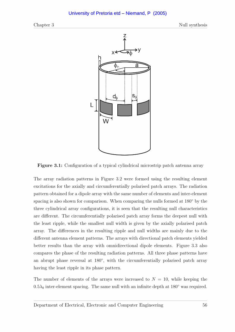
Chapter 3 Null synthesis
Figure 3.1: Configuration of a typical cylindrical microstrip patch antenna array
The array radiation patterns in Figure 3.2 were formed using the resulting element
excitations for the axially and circumferentially polarised patch arrays. The radiation
pattern obtained for a dipole array with the same number of elements and inter-element
spacing is also shown for comparison. When comparing the nulls formed at 180 by the
three cylindrical array configurations, it is seen that the resulting null characteristics
are different. The circumferentially polarised patch array forms the deepest null with
the least ripple, while the smallest null width is given by the axially polarised patch
array. The differences in the resulting ripple and null widths are mainly due to the
different antenna element patterns. The arrays with directional patch elements yielded
better results than the array with omnidirectional dipole elements. Figure 3.3 also
compares the phase of the resulting radiation patterns. All three phase patterns have
an abrupt phase reversal at 180, with the circumferentially polarised patch array
having the least ripple in its phase pattern.
The number of elements of the arrays were increased to N = 10, while keeping the
0.5λ0 inter-element spacing. The same null with an infinite depth at 180 was required.
Department of Electrical, Electronic and Computer Engineering 56
UUnniivveerrssiittyy ooff PPrreettoorriiaa eettdd –– NNiieemmaanndd,, PP ((22000055))
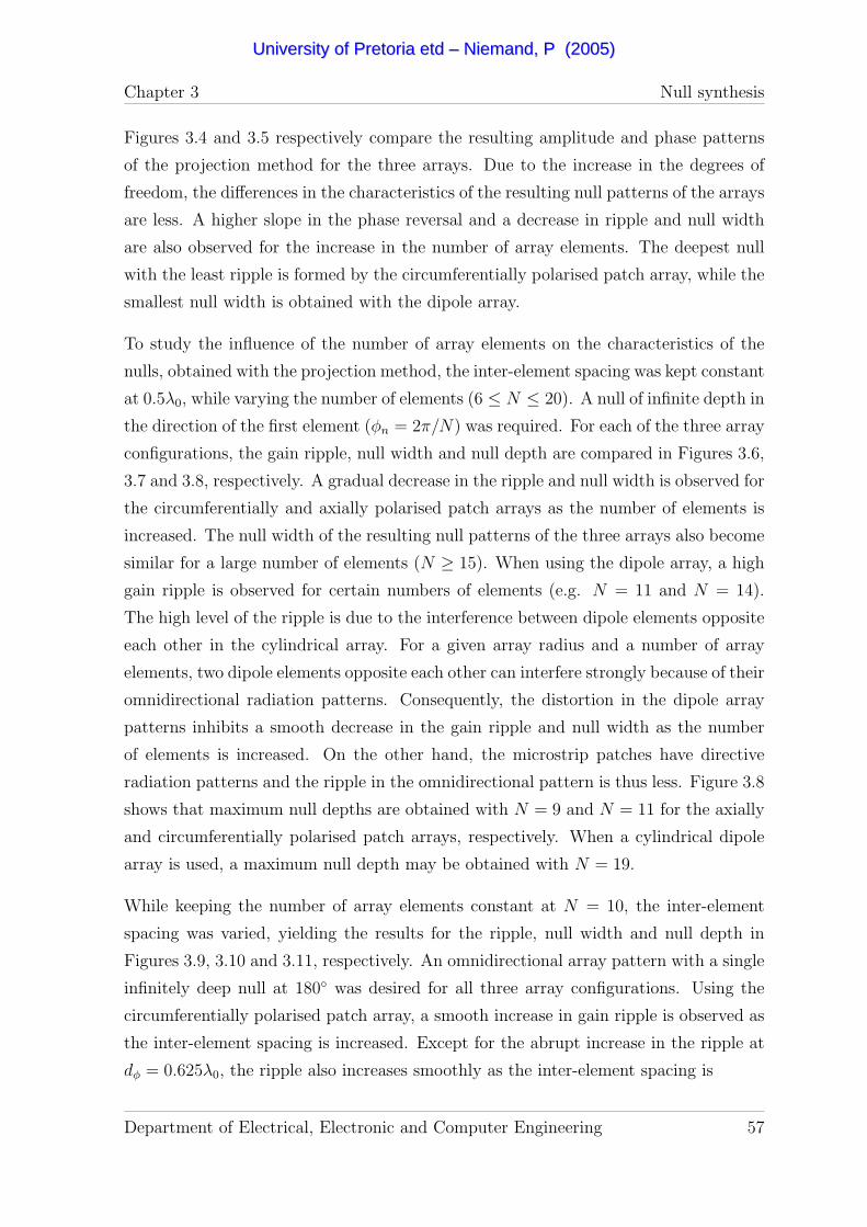
Chapter 3 Null synthesis
Figures 3.4 and 3.5 respectively compare the resulting amplitude and phase patterns
of the projection method for the three arrays. Due to the increase in the degrees of
freedom, the differences in the characteristics of the resulting null patterns of the arrays
are less. A higher slope in the phase reversal and a decrease in ripple and null width
are also observed for the increase in the number of array elements. The deepest null
with the least ripple is formed by the circumferentially polarised patch array, while the
smallest null width is obtained with the dipole array.
To study the influence of the number of array elements on the characteristics of the
nulls, obtained with the projection method, the inter-element spacing was kept constant
at 0.5λ0, while varying the number of elements (6 ≤ N ≤ 20). A null of infinite depth in
the direction of the first element (φn = 2π/N) was required. For each of the three array
configurations, the gain ripple, null width and null depth are compared in Figures 3.6,
3.7 and 3.8, respectively. A gradual decrease in the ripple and null width is observed for
the circumferentially and axially polarised patch arrays as the number of elements is
increased. The null width of the resulting null patterns of the three arrays also become
similar for a large number of elements (N ≥ 15). When using the dipole array, a high
gain ripple is observed for certain numbers of elements (e.g. N = 11 and N = 14).
The high level of the ripple is due to the interference between dipole elements opposite
each other in the cylindrical array. For a given array radius and a number of array
elements, two dipole elements opposite each other can interfere strongly because of their
omnidirectional radiation patterns. Consequently, the distortion in the dipole array
patterns inhibits a smooth decrease in the gain ripple and null width as the number
of elements is increased. On the other hand, the microstrip patches have directive
radiation patterns and the ripple in the omnidirectional pattern is thus less. Figure 3.8
shows that maximum null depths are obtained with N = 9 and N = 11 for the axially
and circumferentially polarised patch arrays, respectively. When a cylindrical dipole
array is used, a maximum null depth may be obtained with N = 19.
While keeping the number of array elements constant at N = 10, the inter-element
spacing was varied, yielding the results for the ripple, null width and null depth in
Figures 3.9, 3.10 and 3.11, respectively. An omnidirectional array pattern with a single
infinitely deep null at 180 was desired for all three array configurations. Using the
circumferentially polarised patch array, a smooth increase in gain ripple is observed as
the inter-element spacing is increased. Except for the abrupt increase in the ripple at
dφ = 0.625λ0, the ripple also increases smoothly as the inter-element spacing is
Department of Electrical, Electronic and Computer Engineering 57
UUnniivveerrssiittyy ooff PPrreettoorriiaa eettdd –– NNiieemmaanndd,, PP ((22000055))

Chapter 3 Null synthesis
-40
-30
-20
-10
0N
orm
alis
ed A
mpl
itud e
(dB
)
0 60 120 180 240 300 360Azimuth Angle (degrees)
Circumferential polAxial polDipole
Figure 3.2: Radiation pattern of a cylindrical array (N=6 and dφ = 0.5λ0) with a
single null
-90
-60
-30
0
30
60
90
Pha s
e (d
egr e
es)
0 60 120 180 240 300 360Azimuth Angle (degrees)
Circumferential polAxial polDipole
Figure 3.3: Phase of the radiation pattern for a cylindrical array (N=6 and
dφ = 0.5λ0) with a single null
Department of Electrical, Electronic and Computer Engineering 58
UUnniivveerrssiittyy ooff PPrreettoorriiaa eettdd –– NNiieemmaanndd,, PP ((22000055))
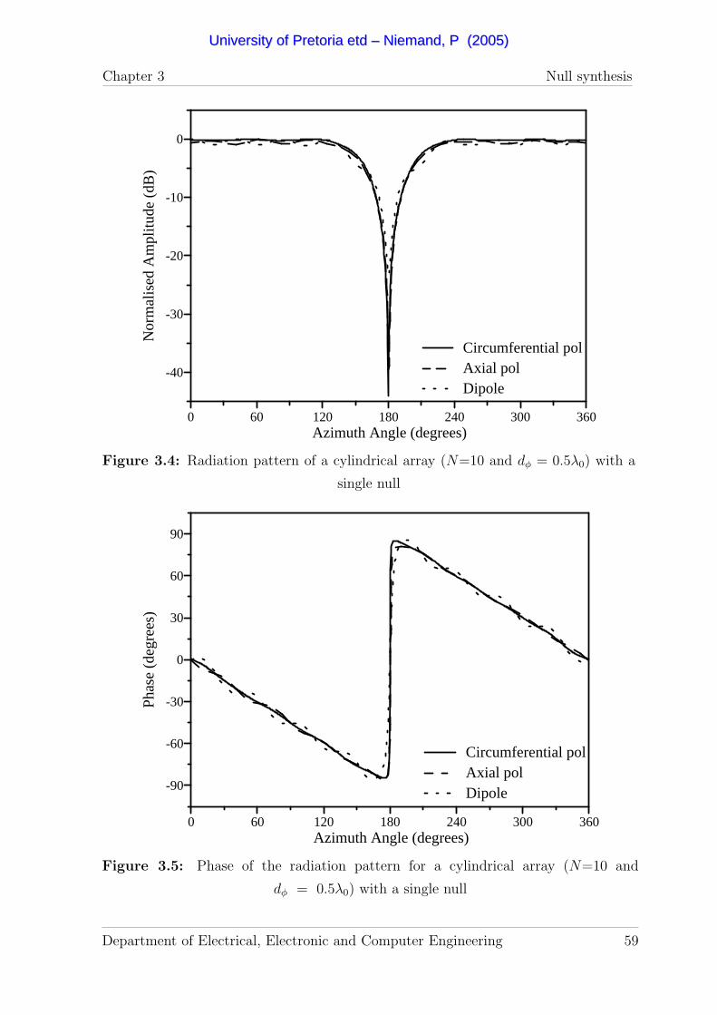
Chapter 3 Null synthesis
-40
-30
-20
-10
0N
orm
alis
ed A
mpl
itud e
(dB
)
0 60 120 180 240 300 360Azimuth Angle (degrees)
Circumferential polAxial polDipole
Figure 3.4: Radiation pattern of a cylindrical array (N=10 and dφ = 0.5λ0) with a
single null
-90
-60
-30
0
30
60
90
Phas
e ( d
egre
es)
0 60 120 180 240 300 360Azimuth Angle (degrees)
Circumferential polAxial polDipole
Figure 3.5: Phase of the radiation pattern for a cylindrical array (N=10 and
dφ = 0.5λ0) with a single null
Department of Electrical, Electronic and Computer Engineering 59
UUnniivveerrssiittyy ooff PPrreettoorriiaa eettdd –– NNiieemmaanndd,, PP ((22000055))
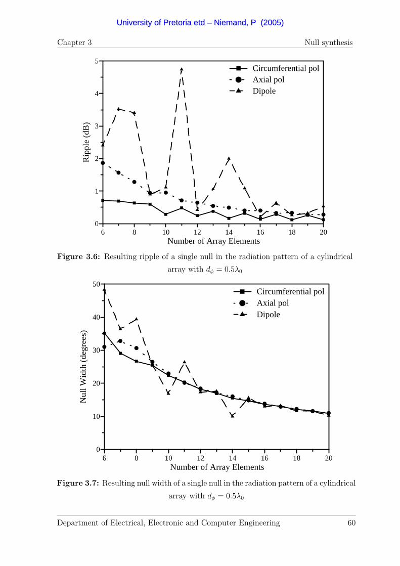
Chapter 3 Null synthesis
0
1
2
3
4
5
Rip
ple
(dB
)
6 8 10 12 14 16 18 20Number of Array Elements
Circumferential polAxial polDipole
Figure 3.6: Resulting ripple of a single null in the radiation pattern of a cylindrical
array with dφ = 0.5λ0
0
10
20
30
40
50
Nul
l Wid
th (
d egr
ees)
6 8 10 12 14 16 18 20Number of Array Elements
Circumferential polAxial polDipole
Figure 3.7: Resulting null width of a single null in the radiation pattern of a cylindrical
array with dφ = 0.5λ0
Department of Electrical, Electronic and Computer Engineering 60
UUnniivveerrssiittyy ooff PPrreettoorriiaa eettdd –– NNiieemmaanndd,, PP ((22000055))

Chapter 3 Null synthesis
0
10
20
30
40
50
60
Nu l
l dep
th (
dB)
6 8 10 12 14 16 18 20Number of Array Elements
Circumferential polAxial polDipole
Figure 3.8: Resulting null depth of a single null in the radiation pattern of a cylindrical
array with dφ = 0.5λ0
0
2
4
6
8
10
Rip
ple
(dB
)
0.30 0.40 0.50 0.60 0.70Inter-element spacing (wavelengths)
Circumferential polAxial polDipole
Figure 3.9: Resulting ripple of a single null in the radiation pattern of a cylindrical
array with N = 10
Department of Electrical, Electronic and Computer Engineering 61
UUnniivveerrssiittyy ooff PPrreettoorriiaa eettdd –– NNiieemmaanndd,, PP ((22000055))

Chapter 3 Null synthesis
10
15
20
25
30
35
40
Nul
l Wid
th (
d egr
ees)
0.30 0.40 0.50 0.60 0.70Inter-element Spacing (wavelengths)
Circumferential polAxial polDipole
Figure 3.10: Resulting null width of a single null in the radiation pattern of a cylin-
drical array with N = 10
10
20
30
40
50
60
70
80
Nu l
l dep
th (
dB)
0.30 0.40 0.50 0.60 0.70Inter-element spacing (wavelengths)
Circumferential polAxial polDipole
Figure 3.11: Resulting null depth of a single null in the radiation pattern of a cylin-
drical array with N = 10
Department of Electrical, Electronic and Computer Engineering 62
UUnniivveerrssiittyy ooff PPrreettoorriiaa eettdd –– NNiieemmaanndd,, PP ((22000055))

Chapter 3 Null synthesis
increased in the axially polarised patch array. In contrast to the behaviour of the patch
arrays, the gain ripple in the amplitude pattern of the dipole array depends highly on
the inter-element spacing. For certain inter-element spacings, the interference between
the elements yields large gain ripple values.
Figure 3.10 shows that the null widths of the resulting nulls increase gradually as the
inter-element spacing is increased in both patch arrays. On the other hand, the utilisa-
tion of the dipole array may result in a maximum or minimum null width, depending
on the inter-element spacing. All three arrays yield different null depth results using
the orthogonal projection method, as seen in Figure 3.11. A maximum null depth of
49 dB at dφ = 0.465λ0 may be obtained with the circumferentially polarised patch
array. With the axially polarised patch array a maximum null depth of 64 dB can be
obtained at dφ = 0.55λ0, while the dipole array yields a maximum null depth of 71 dB
at dφ = 0.61λ0.
3.2 Objective weighting method
The orthogonal projection method provides an optimal array pattern with the least
pattern error (in a least square sense). The optimal array pattern may not have the
desired pattern characteristics, since the amplitude and phase of the radiation pattern
are optimised simultaneously. Some of the amplitude pattern characteristics may be
improved by applying a windowing function to the resulting element excitations. While
some characteristics may improve, other characteristics are degraded.
This implies that a multi-objective optimisation approach has to be followed. In stead
of minimising the array pattern error, a global performance function can be defined
by utilising the amplitude pattern error and the phase pattern error. The minimum of
this performance function is then sought after.
3.2.1 Performance function and Pareto optimality
In the objective weighting method a global performance function is obtained by means
of a linear combination of the multi-objective functions of the optimisation scenario [97].
Department of Electrical, Electronic and Computer Engineering 63
UUnniivveerrssiittyy ooff PPrreettoorriiaa eettdd –– NNiieemmaanndd,, PP ((22000055))

Chapter 3 Null synthesis
The performance function for an array pattern may be defined as:
P = c1ea + c2ep, (3.1)
where c1 and c2 are weighting factors and ea and ep are the amplitude and phase pattern
errors, respectively. The amplitude pattern error ea is defined as:
ea(A) =
2π∫
0
(|F (φ;A)| − |F0(φ)|)2dφ, (3.2)
while the phase pattern error ep is defined as:
ep(A) =
2π∫
0
(6 F (φ;A)− 6 F0(φ))2dφ. (3.3)
The multi-objective optimisation problem can be solved by finding the minimum of
P . Using the above definition, P will be independent of the minima of the objective
functions ea and ep. It can also be observed from Equation 3.1, that the resulting
values of ea and ep, which are obtained after finding the minimum of P , will depend
on the ratio c2/c1. Thus, the ratio c2/c1 should be properly defined. The critical value
of the ratio c2/c1 can be obtained through observing the behaviour of ea and ep when
minimising different performance functions.
Figure 3.12 illustrates an example of an optimisation problem with different minima in
a criterion space for different performance function definitions. The minima of P was
found for different ratios c2/c1, which is indicated on the graph. For each minimum, the
resulting values of ea and ep is shown. The curve formed by the resulting ea and ep is
referred to as the Pareto optimal front which contains Pareto optimal points. A Pareto
optimal point has been obtained when no other points exist in the variable domain for
which the value of one of the two objective functions decreases and the other function
does not increase [95–97]. The critical ratio (0.5), where√
(e2a + e2
p) is at a minimum,
is circled on the graph. This Pareto optimal point is the most reasonable choice in
a least square sense when trying to minimise both the amplitude and phase pattern
errors.
The objective weighting method can thus be applied in a null synthesis technique
to improve the amplitude pattern and consequently the amplitude pattern error. As
indicated by the Pareto optimal front, the trade-off will be a gain in the phase pattern
error for a loss in the amplitude pattern error.
Department of Electrical, Electronic and Computer Engineering 64
UUnniivveerrssiittyy ooff PPrreettoorriiaa eettdd –– NNiieemmaanndd,, PP ((22000055))
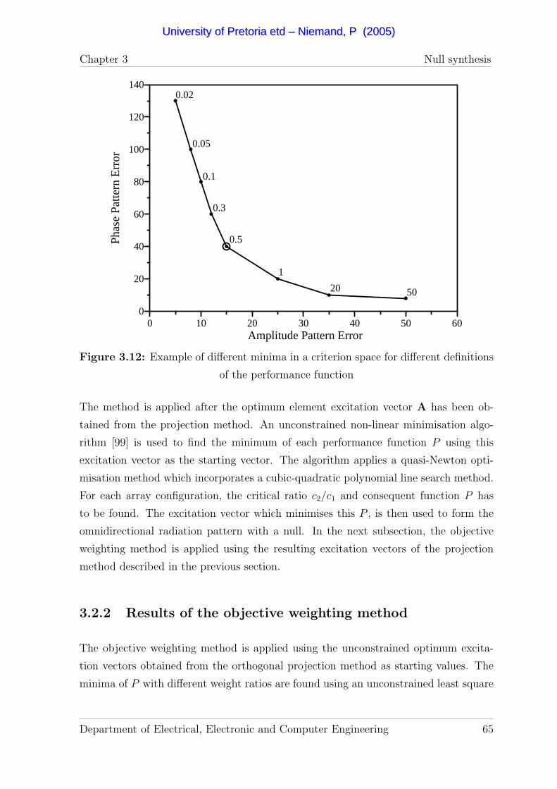
Chapter 3 Null synthesis
0
20
40
60
80
100
120
140
P has
e Pa
ttern
Err
or
0 10 20 30 40 50 60Amplitude Pattern Error
0.5
0.1
50
1
0.3
20
0.02
0.05
Figure 3.12: Example of different minima in a criterion space for different definitions
of the performance function
The method is applied after the optimum element excitation vector A has been ob-
tained from the projection method. An unconstrained non-linear minimisation algo-
rithm [99] is used to find the minimum of each performance function P using this
excitation vector as the starting vector. The algorithm applies a quasi-Newton opti-
misation method which incorporates a cubic-quadratic polynomial line search method.
For each array configuration, the critical ratio c2/c1 and consequent function P has
to be found. The excitation vector which minimises this P , is then used to form the
omnidirectional radiation pattern with a null. In the next subsection, the objective
weighting method is applied using the resulting excitation vectors of the projection
method described in the previous section.
3.2.2 Results of the objective weighting method
The objective weighting method is applied using the unconstrained optimum excita-
tion vectors obtained from the orthogonal projection method as starting values. The
minima of P with different weight ratios are found using an unconstrained least square
Department of Electrical, Electronic and Computer Engineering 65
UUnniivveerrssiittyy ooff PPrreettoorriiaa eettdd –– NNiieemmaanndd,, PP ((22000055))
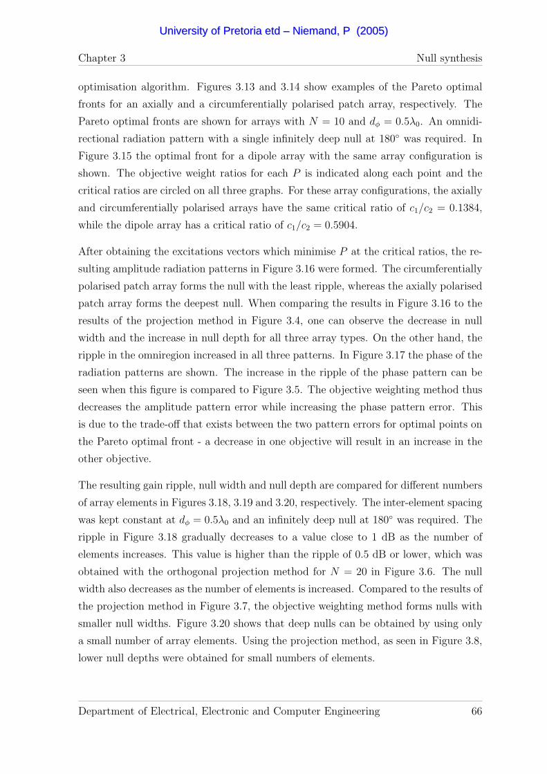
Chapter 3 Null synthesis
optimisation algorithm. Figures 3.13 and 3.14 show examples of the Pareto optimal
fronts for an axially and a circumferentially polarised patch array, respectively. The
Pareto optimal fronts are shown for arrays with N = 10 and dφ = 0.5λ0. An omnidi-
rectional radiation pattern with a single infinitely deep null at 180 was required. In
Figure 3.15 the optimal front for a dipole array with the same array configuration is
shown. The objective weight ratios for each P is indicated along each point and the
critical ratios are circled on all three graphs. For these array configurations, the axially
and circumferentially polarised arrays have the same critical ratio of c1/c2 = 0.1384,
while the dipole array has a critical ratio of c1/c2 = 0.5904.
After obtaining the excitations vectors which minimise P at the critical ratios, the re-
sulting amplitude radiation patterns in Figure 3.16 were formed. The circumferentially
polarised patch array forms the null with the least ripple, whereas the axially polarised
patch array forms the deepest null. When comparing the results in Figure 3.16 to the
results of the projection method in Figure 3.4, one can observe the decrease in null
width and the increase in null depth for all three array types. On the other hand, the
ripple in the omniregion increased in all three patterns. In Figure 3.17 the phase of the
radiation patterns are shown. The increase in the ripple of the phase pattern can be
seen when this figure is compared to Figure 3.5. The objective weighting method thus
decreases the amplitude pattern error while increasing the phase pattern error. This
is due to the trade-off that exists between the two pattern errors for optimal points on
the Pareto optimal front - a decrease in one objective will result in an increase in the
other objective.
The resulting gain ripple, null width and null depth are compared for different numbers
of array elements in Figures 3.18, 3.19 and 3.20, respectively. The inter-element spacing
was kept constant at dφ = 0.5λ0 and an infinitely deep null at 180 was required. The
ripple in Figure 3.18 gradually decreases to a value close to 1 dB as the number of
elements increases. This value is higher than the ripple of 0.5 dB or lower, which was
obtained with the orthogonal projection method for N = 20 in Figure 3.6. The null
width also decreases as the number of elements is increased. Compared to the results of
the projection method in Figure 3.7, the objective weighting method forms nulls with
smaller null widths. Figure 3.20 shows that deep nulls can be obtained by using only
a small number of array elements. Using the projection method, as seen in Figure 3.8,
lower null depths were obtained for small numbers of elements.
Department of Electrical, Electronic and Computer Engineering 66
UUnniivveerrssiittyy ooff PPrreettoorriiaa eettdd –– NNiieemmaanndd,, PP ((22000055))

Chapter 3 Null synthesis
0
20
40
60
80
100
120
140
Phas
e Pa
ttern
Err
or
0 10 20 30 40 50 60Amplitude Pattern Error
0.3184
0.152
501
0.1667
2
0.05
Figure 3.13: Minima for different definitions of the performance function for a cylin-
drical array of axially polarised patches with N = 10 and dφ = 0.5λ0
0
20
40
60
80
100
120
140
Phas
e Pa
ttern
Err
or
0 10 20 30 40 50 60Amplitude Pattern Error
0.3184
0.1995
501 2
0.2222
0.1
0.05
Figure 3.14: Minima for different definitions of the performance function for a cylin-
drical array of circumferentially polarised patches with N = 10 and dφ = 0.5λ0
Department of Electrical, Electronic and Computer Engineering 67
UUnniivveerrssiittyy ooff PPrreettoorriiaa eettdd –– NNiieemmaanndd,, PP ((22000055))

Chapter 3 Null synthesis
0
20
40
60
80
100
120
140
Phas
e Pa
ttern
Err
or
0 20 40 60 80 100 120 140Amplitude Pattern Error
0.5904
0.1
501
100
0.05
0.1667
0.25
2
0.37
25
Figure 3.15: Minima for different definitions of the performance function for a cylin-
drical array of dipoles with N = 10 and dφ = 0.5λ0
While keeping the number of array elements constant at N = 10, the inter-element
spacing of the arrays was varied. The resulting ripple, null width and null depth are
compared for the different types of arrays in Figures 3.21, 3.22 and 3.22, respectively.
For the dipole array with dφ = 0.55λ0, the objective weighting function could not yield
a critical ratio value for P due to the high ripple in the omni-region. No results for
this inter-element spacing could thus be shown in the figures.
For patch arrays with dφ ≥ 0.45λ0, the ripple increases as the inter-element spacing is
increased in Figure 3.21. In Figure 3.22, the resulting null width for a circumferentially
polarised patch array decreases as the inter-element spacing increases for dφ ≤ 0.55λ0.
For dφ ≥ 0.6λ0, the null width starts to increase for increasing inter-element spacing.
The null width for an axially polarised patch array firstly decreases with increasing
inter-element spacing up to dφ = 0.5λ0 before it increases for increasing inter-element
spacing. Using the objective weighting method, maximum null depths can be obtained
with inter-element spacings of dφ = 0.625λ0 and dφ = 0.675λ0 for circumferentially and
axially polarised patch arrays, respectively.
Department of Electrical, Electronic and Computer Engineering 68
UUnniivveerrssiittyy ooff PPrreettoorriiaa eettdd –– NNiieemmaanndd,, PP ((22000055))
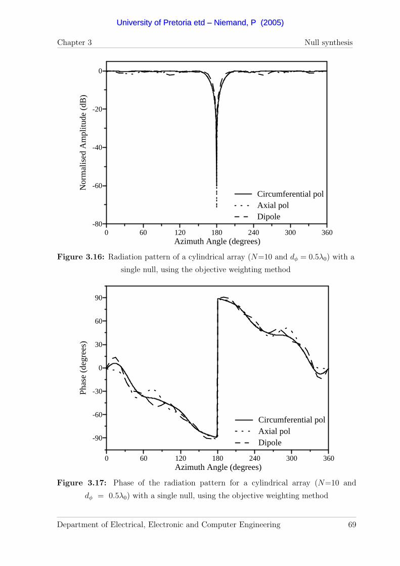
Chapter 3 Null synthesis
-80
-60
-40
-20
0
Nor
mal
ised
Am
plitu
d e (
dB)
0 60 120 180 240 300 360Azimuth Angle (degrees)
Circumferential polAxial polDipole
Figure 3.16: Radiation pattern of a cylindrical array (N=10 and dφ = 0.5λ0) with a
single null, using the objective weighting method
-90
-60
-30
0
30
60
90
Phas
e ( d
egre
es)
0 60 120 180 240 300 360Azimuth Angle (degrees)
Circumferential polAxial polDipole
Figure 3.17: Phase of the radiation pattern for a cylindrical array (N=10 and
dφ = 0.5λ0) with a single null, using the objective weighting method
Department of Electrical, Electronic and Computer Engineering 69
UUnniivveerrssiittyy ooff PPrreettoorriiaa eettdd –– NNiieemmaanndd,, PP ((22000055))
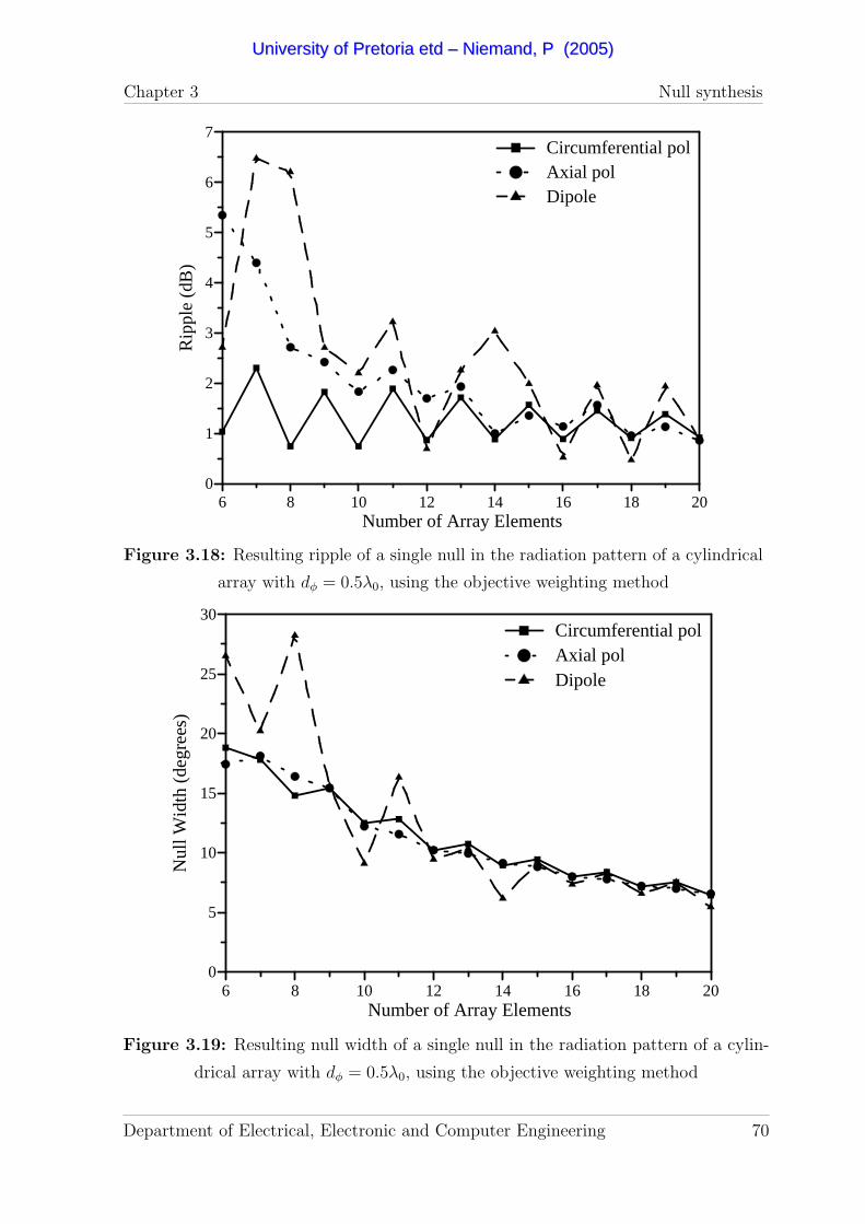
Chapter 3 Null synthesis
0
1
2
3
4
5
6
7
Rip
ple
(dB
)
6 8 10 12 14 16 18 20Number of Array Elements
Circumferential polAxial polDipole
Figure 3.18: Resulting ripple of a single null in the radiation pattern of a cylindrical
array with dφ = 0.5λ0, using the objective weighting method
0
5
10
15
20
25
30
Nul
l Wid
th (
d egr
ees)
6 8 10 12 14 16 18 20Number of Array Elements
Circumferential polAxial polDipole
Figure 3.19: Resulting null width of a single null in the radiation pattern of a cylin-
drical array with dφ = 0.5λ0, using the objective weighting method
Department of Electrical, Electronic and Computer Engineering 70
UUnniivveerrssiittyy ooff PPrreettoorriiaa eettdd –– NNiieemmaanndd,, PP ((22000055))
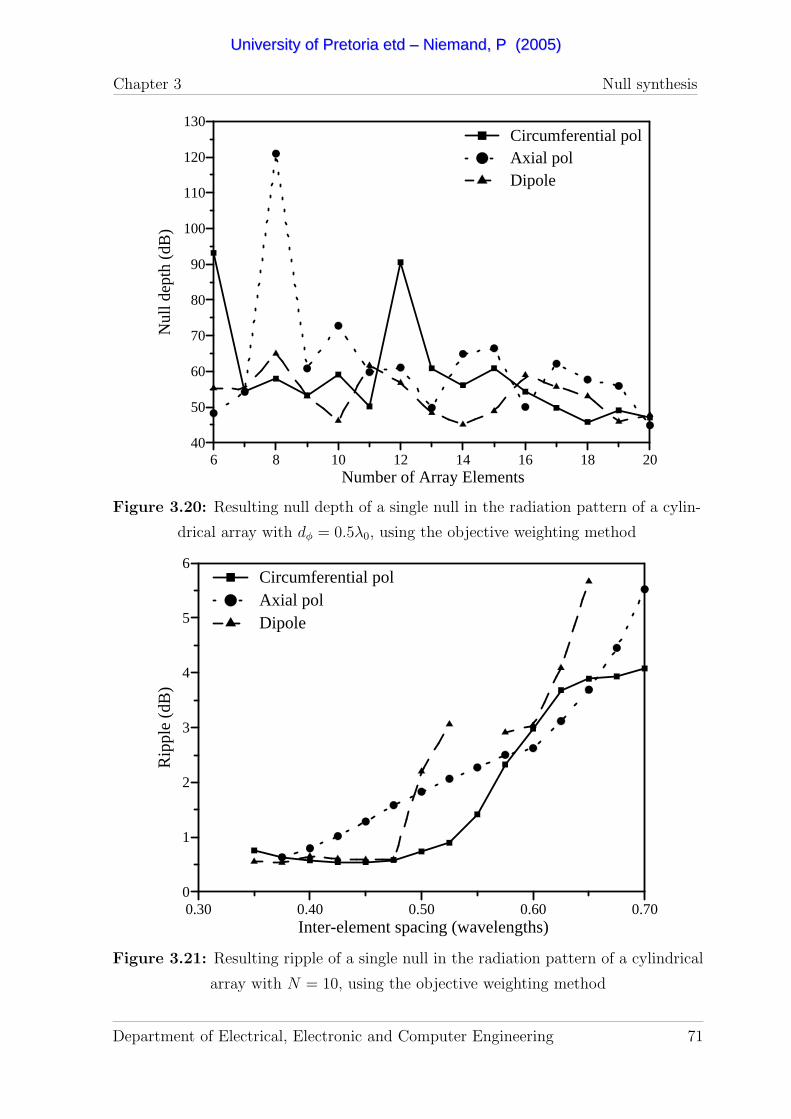
Chapter 3 Null synthesis
40
50
60
70
80
90
100
110
120
130
Nul
l dep
th (
dB)
6 8 10 12 14 16 18 20Number of Array Elements
Circumferential polAxial polDipole
Figure 3.20: Resulting null depth of a single null in the radiation pattern of a cylin-
drical array with dφ = 0.5λ0, using the objective weighting method
0
1
2
3
4
5
6
Rip
ple
(dB
)
0.30 0.40 0.50 0.60 0.70Inter-element spacing (wavelengths)
Circumferential polAxial polDipole
Figure 3.21: Resulting ripple of a single null in the radiation pattern of a cylindrical
array with N = 10, using the objective weighting method
Department of Electrical, Electronic and Computer Engineering 71
UUnniivveerrssiittyy ooff PPrreettoorriiaa eettdd –– NNiieemmaanndd,, PP ((22000055))
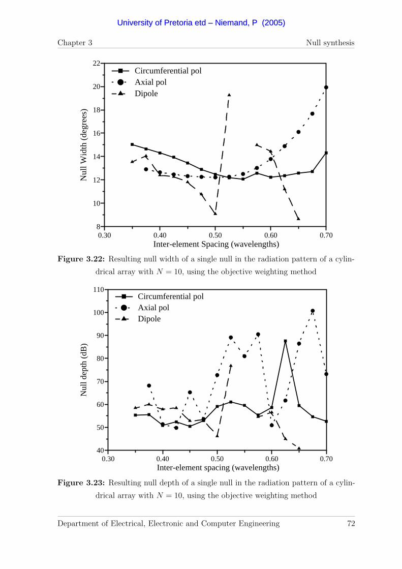
Chapter 3 Null synthesis
8
10
12
14
16
18
20
22
Nul
l Wid
th (
d egr
ees)
0.30 0.40 0.50 0.60 0.70Inter-element Spacing (wavelengths)
Circumferential polAxial polDipole
Figure 3.22: Resulting null width of a single null in the radiation pattern of a cylin-
drical array with N = 10, using the objective weighting method
40
50
60
70
80
90
100
110
Nul
l dep
th (
dB)
0.30 0.40 0.50 0.60 0.70Inter-element spacing (wavelengths)
Circumferential polAxial polDipole
Figure 3.23: Resulting null depth of a single null in the radiation pattern of a cylin-
drical array with N = 10, using the objective weighting method
Department of Electrical, Electronic and Computer Engineering 72
UUnniivveerrssiittyy ooff PPrreettoorriiaa eettdd –– NNiieemmaanndd,, PP ((22000055))

Chapter 3 Null synthesis
3.3 Constrained optimisation
The objective weighting method provides a way of improving the characteristics of the
amplitude radiation pattern. This improvement is mostly manifested in a decreased
null width and an increased null depth when an infinitely deep null is considered. On
the other hand, the gain ripple in the omni-region increases.
Another way of improving the resulting amplitude pattern would be to provide con-
trol over the individual characteristics. In some applications, the degree of suppres-
sion needs to be specified through a controllable null depth. As discussed previously,
Abele [54] proposed a variable phase step to provide control over the null depth. The
accuracy of the resulting null depth depends on the array configuration and the desired
null depth.
Constrained optimisation provides a method of constraining the different attributes of
the amplitude pattern while minimising the array pattern error. All the attributes or
combinations of attributes can thus be controlled.
3.3.1 Results of the constrained optimisation
A constrained optimisation algorithm [99] is employed to find an excitation vector
which yields the minimum pattern error under the constraints specified for certain
amplitude pattern characteristics. The choice of the starting values for the excitations
vector fulfils a very important role in the success of the optimisation. When these
values are chosen carefully, the optimisation time can be limited and local minima can
be avoided. The excitation vector obtained from the orthogonal projection method
yields an optimum radiation pattern with the minimum pattern error and is therefore
chosen as the starting value. The resulting vector from the constrained optimisation will
produce a radiation pattern with a pattern error as close as possible to this minimum
pattern error while satisfying the constraints.
The algorithm allows the placement of constraints on the gain ripple, the null depth
and the null width. These constraints are set equal to the desired values of the char-
acteristics. Two additional constraints are also placed on the amplitudes and phases
of the element excitations:
|an| ≤ 1, (3.4)
Department of Electrical, Electronic and Computer Engineering 73
UUnniivveerrssiittyy ooff PPrreettoorriiaa eettdd –– NNiieemmaanndd,, PP ((22000055))
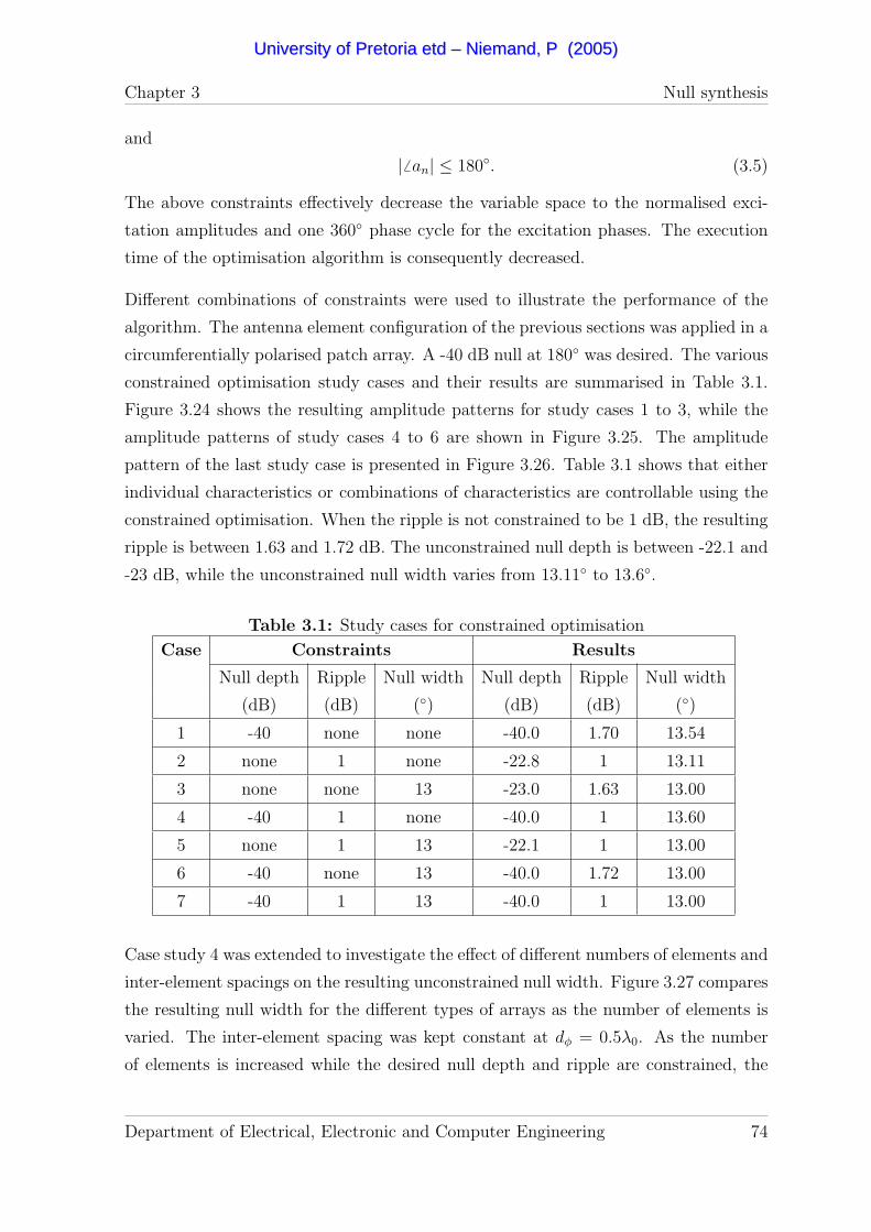
Chapter 3 Null synthesis
and
| 6 an| ≤ 180. (3.5)
The above constraints effectively decrease the variable space to the normalised exci-
tation amplitudes and one 360 phase cycle for the excitation phases. The execution
time of the optimisation algorithm is consequently decreased.
Different combinations of constraints were used to illustrate the performance of the
algorithm. The antenna element configuration of the previous sections was applied in a
circumferentially polarised patch array. A -40 dB null at 180 was desired. The various
constrained optimisation study cases and their results are summarised in Table 3.1.
Figure 3.24 shows the resulting amplitude patterns for study cases 1 to 3, while the
amplitude patterns of study cases 4 to 6 are shown in Figure 3.25. The amplitude
pattern of the last study case is presented in Figure 3.26. Table 3.1 shows that either
individual characteristics or combinations of characteristics are controllable using the
constrained optimisation. When the ripple is not constrained to be 1 dB, the resulting
ripple is between 1.63 and 1.72 dB. The unconstrained null depth is between -22.1 and
-23 dB, while the unconstrained null width varies from 13.11 to 13.6.
Table 3.1: Study cases for constrained optimisation
Case Constraints Results
Null depth Ripple Null width Null depth Ripple Null width
(dB) (dB) () (dB) (dB) ()
1 -40 none none -40.0 1.70 13.54
2 none 1 none -22.8 1 13.11
3 none none 13 -23.0 1.63 13.00
4 -40 1 none -40.0 1 13.60
5 none 1 13 -22.1 1 13.00
6 -40 none 13 -40.0 1.72 13.00
7 -40 1 13 -40.0 1 13.00
Case study 4 was extended to investigate the effect of different numbers of elements and
inter-element spacings on the resulting unconstrained null width. Figure 3.27 compares
the resulting null width for the different types of arrays as the number of elements is
varied. The inter-element spacing was kept constant at dφ = 0.5λ0. As the number
of elements is increased while the desired null depth and ripple are constrained, the
Department of Electrical, Electronic and Computer Engineering 74
UUnniivveerrssiittyy ooff PPrreettoorriiaa eettdd –– NNiieemmaanndd,, PP ((22000055))

Chapter 3 Null synthesis
null width gradually decreases. Arrays with an uneven number of elements produce
wider null widths than arrays with an even number of elements for N ≥ 9. The
circumferentially and axially polarised patch arrays show similar null widths for N >
11, while for a large number of array elements (N > 16), the null widths of all three
arrays become similar.
While keeping the number of elements constant at N = 10, the inter-element spacing
was varied, yielding the results in Figure 3.28. Due to the high distortion in the far-
field of the dipole array, a gain ripple of less than 1 dB could not be obtained with
the dipole array, while the axially and circumferentially polarised patch arrays could
not form the null with a 1 dB ripple for dφ > 0.65λ0 and dφ > 0.675λ0, respectively.
The circumferentially polarised patch array patterns have the smallest null widths for
dφ > 0.5λ0.
-40
-30
-20
-10
0
Nor
mal
ised
Am
plitu
d e (
dB)
0 60 120 180 240 300 360Azimuth Angle (degrees)
Case 1Case 2Case 3
Figure 3.24: Radiation pattern of a cylindrical array (N=10 and dφ = 0.5λ0) with a
single null, using the constrained optimisation method for cases 1, 2 and 3
Department of Electrical, Electronic and Computer Engineering 75
UUnniivveerrssiittyy ooff PPrreettoorriiaa eettdd –– NNiieemmaanndd,, PP ((22000055))

Chapter 3 Null synthesis
-40
-30
-20
-10
0N
orm
alis
ed A
mpl
itud e
(dB
)
0 60 120 180 240 300 360Azimuth Angle (degrees)
Case 4Case 5Case 6
Figure 3.25: Radiation pattern of a cylindrical array (N=10 and dφ = 0.5λ0) with a
single null, using the constrained optimisation method for cases 4, 5 and 6
-40
-30
-20
-10
0
Nor
mal
ised
Am
plitu
d e (
dB)
0 60 120 180 240 300 360Azimuth Angle (degrees)
Figure 3.26: Radiation pattern of a cylindrical array (N=10 and dφ = 0.5λ0) with a
single null, using the constrained optimisation method for case 7
Department of Electrical, Electronic and Computer Engineering 76
UUnniivveerrssiittyy ooff PPrreettoorriiaa eettdd –– NNiieemmaanndd,, PP ((22000055))
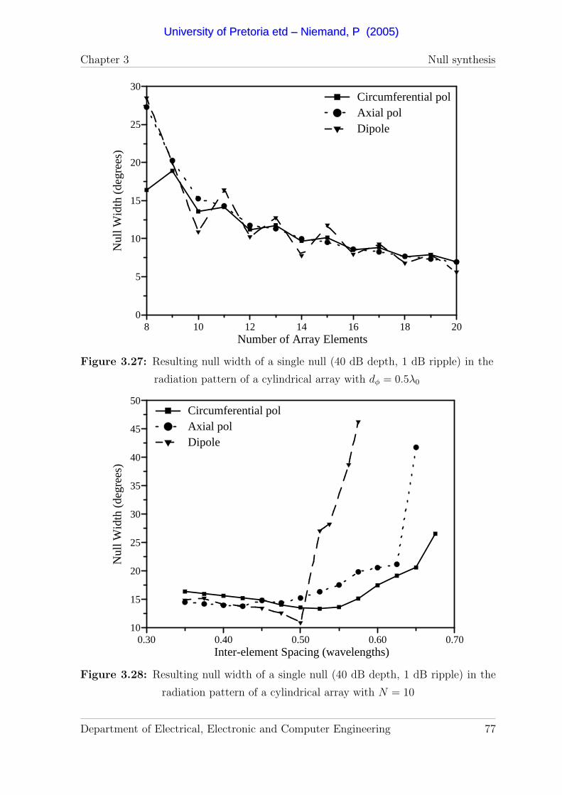
Chapter 3 Null synthesis
0
5
10
15
20
25
30
Nul
l Wid
th (
d egr
ees)
8 10 12 14 16 18 20Number of Array Elements
Circumferential polAxial polDipole
Figure 3.27: Resulting null width of a single null (40 dB depth, 1 dB ripple) in the
radiation pattern of a cylindrical array with dφ = 0.5λ0
10
15
20
25
30
35
40
45
50
Nul
l Wid
th (
d egr
ees)
0.30 0.40 0.50 0.60 0.70Inter-element Spacing (wavelengths)
Circumferential polAxial polDipole
Figure 3.28: Resulting null width of a single null (40 dB depth, 1 dB ripple) in the
radiation pattern of a cylindrical array with N = 10
Department of Electrical, Electronic and Computer Engineering 77
UUnniivveerrssiittyy ooff PPrreettoorriiaa eettdd –– NNiieemmaanndd,, PP ((22000055))

Chapter 3 Null synthesis
3.4 Comparison of null synthesis methods
Each of the optimisation methods proposed in the previous sections have different
advantages and disadvantages. To compare the results of the three methods, a single
-40 dB null at 180 was specified as the desired null. The orthogonal projection method
was used to obtain the starting excitation vector for all the methods. The results of the
different optimisation methods for different types of arrays (N = 10 and dφ = 0.5λ0) are
compared in Table 3.2. In the first method, a window function was applied to reduce the
ripple in the omni-region. Figures 3.29, 3.30 and 3.31 compare the resulting amplitude
patterns of the first three optimisation methods for a circumferentially polarised patch
array, an axially polarised patch array and a dipole array, respectively.
For each array configuration, the projection method forms the null with the least gain
ripple, but with the largest null width. The objective weighting method produces a
null with the least null width, but the resulting null is deeper than required. When
the constrained method is used with only one constraint placed on the null depth,
the resulting gain ripple for the patch arrays is higher than the gain ripple obtained
from the projection and objective weighting methods. The obtained null width is
also slightly higher than the null width produced by the objective weighting method.
By constraining the ripple as well, the null width remains almost the same for the
circumferentially polarised patch array, but slightly increases for the axially polarised
patch array.
When only a low gain ripple is of concern, the orthogonal projection method with a
window function can be used. On the other hand, the objective weighting method can
be applied to obtain a narrow null when a higher gain ripple is tolerable. The resulting
null depth for these two methods will depend on the number of elements as well as the
inter-element spacing. The constrained optimisation method can be used to control
both the null depth and the ripple, while obtaining a null width close to the null width
resulting from the objective weighting method.
In the next section, the constrained optimisation method will be used to form multiple
nulls in an otherwise omnidirectional pattern.
Department of Electrical, Electronic and Computer Engineering 78
UUnniivveerrssiittyy ooff PPrreettoorriiaa eettdd –– NNiieemmaanndd,, PP ((22000055))
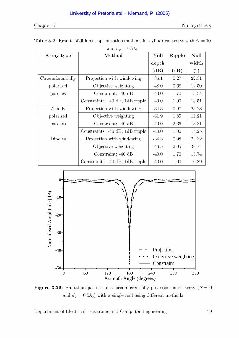
Chapter 3 Null synthesis
Table 3.2: Results of different optimisation methods for cylindrical arrays with N = 10
and dφ = 0.5λ0
Array type Method Null Ripple Null
depth width
(dB) (dB) ()
Circumferentially Projection with windowing -36.1 0.27 22.31
polarised Objective weighting -48.0 0.68 12.50
patches Constraint: -40 dB -40.0 1.70 13.54
Constraints: -40 dB, 1dB ripple -40.0 1.00 13.51
Axially Projection with windowing -34.3 0.97 23.28
polarised Objective weighting -81.9 1.85 12.21
patches Constraint: -40 dB -40.0 2.66 13.81
Constraints: -40 dB, 1dB ripple -40.0 1.00 15.25
Dipoles Projection with windowing -34.3 0.98 23.32
Objective weighting -46.5 2.05 9.10
Constraint: -40 dB -40.0 1.70 13.74
Constraints: -40 dB, 1dB ripple -40.0 1.00 10.89
-50
-40
-30
-20
-10
0
Nor
mal
ised
Am
plitu
d e (
dB)
0 60 120 180 240 300 360Azimuth Angle (degrees)
ProjectionObjective weightingConstraint
Figure 3.29: Radiation pattern of a circumferentially polarised patch array (N=10
and dφ = 0.5λ0) with a single null using different methods
Department of Electrical, Electronic and Computer Engineering 79
UUnniivveerrssiittyy ooff PPrreettoorriiaa eettdd –– NNiieemmaanndd,, PP ((22000055))
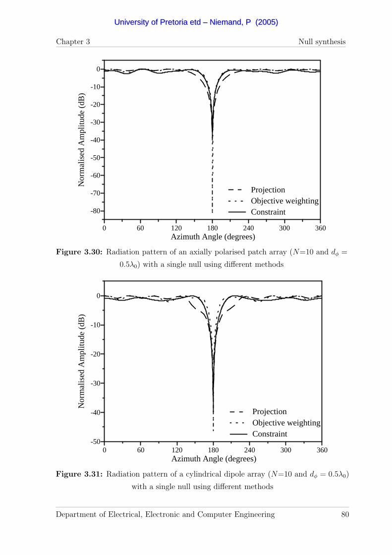
Chapter 3 Null synthesis
-80
-70
-60
-50
-40
-30
-20
-10
0
Nor
mal
ised
Am
plitu
d e (
dB)
0 60 120 180 240 300 360Azimuth Angle (degrees)
ProjectionObjective weightingConstraint
Figure 3.30: Radiation pattern of an axially polarised patch array (N=10 and dφ =
0.5λ0) with a single null using different methods
-50
-40
-30
-20
-10
0
Nor
mal
ised
Am
plitu
d e (
dB)
0 60 120 180 240 300 360Azimuth Angle (degrees)
ProjectionObjective weightingConstraint
Figure 3.31: Radiation pattern of a cylindrical dipole array (N=10 and dφ = 0.5λ0)
with a single null using different methods
Department of Electrical, Electronic and Computer Engineering 80
UUnniivveerrssiittyy ooff PPrreettoorriiaa eettdd –– NNiieemmaanndd,, PP ((22000055))
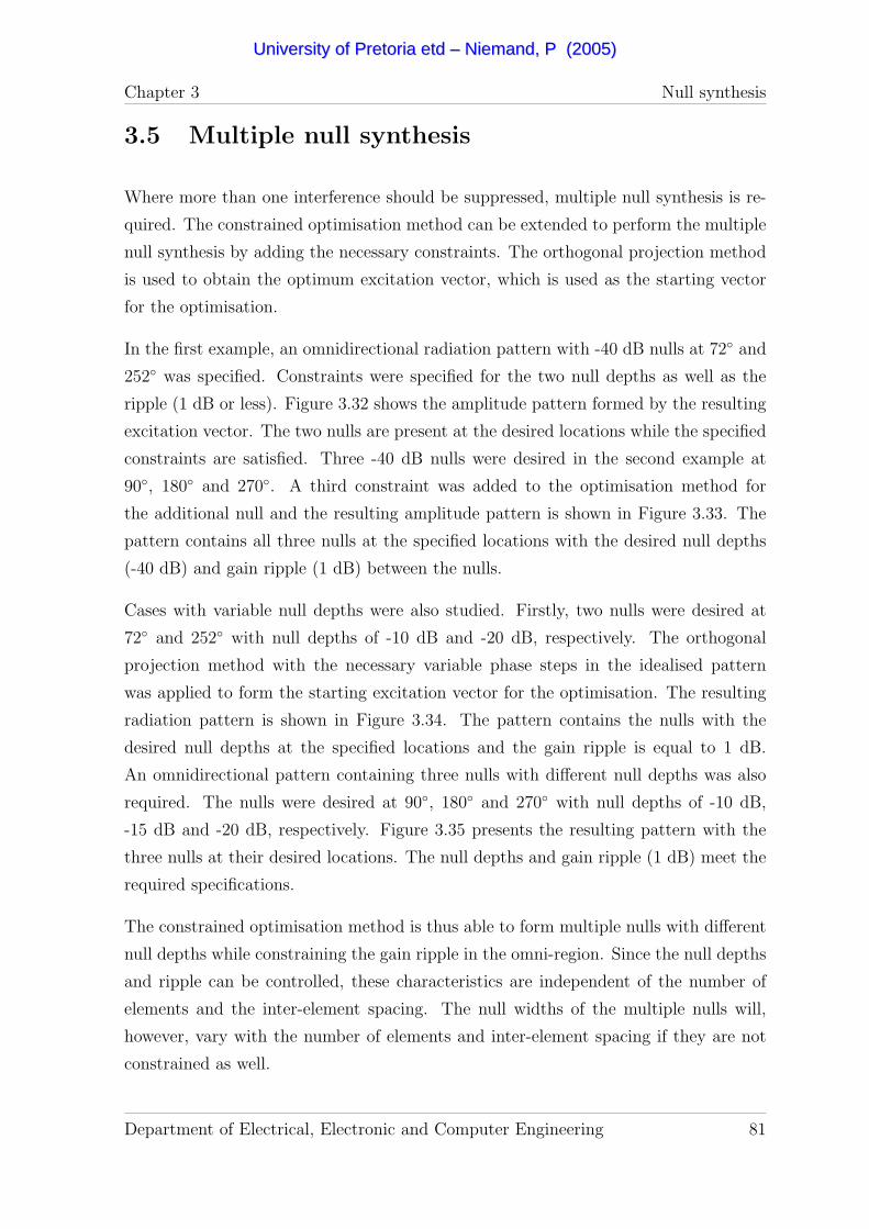
Chapter 3 Null synthesis
3.5 Multiple null synthesis
Where more than one interference should be suppressed, multiple null synthesis is re-
quired. The constrained optimisation method can be extended to perform the multiple
null synthesis by adding the necessary constraints. The orthogonal projection method
is used to obtain the optimum excitation vector, which is used as the starting vector
for the optimisation.
In the first example, an omnidirectional radiation pattern with -40 dB nulls at 72 and
252 was specified. Constraints were specified for the two null depths as well as the
ripple (1 dB or less). Figure 3.32 shows the amplitude pattern formed by the resulting
excitation vector. The two nulls are present at the desired locations while the specified
constraints are satisfied. Three -40 dB nulls were desired in the second example at
90, 180 and 270. A third constraint was added to the optimisation method for
the additional null and the resulting amplitude pattern is shown in Figure 3.33. The
pattern contains all three nulls at the specified locations with the desired null depths
(-40 dB) and gain ripple (1 dB) between the nulls.
Cases with variable null depths were also studied. Firstly, two nulls were desired at
72 and 252 with null depths of -10 dB and -20 dB, respectively. The orthogonal
projection method with the necessary variable phase steps in the idealised pattern
was applied to form the starting excitation vector for the optimisation. The resulting
radiation pattern is shown in Figure 3.34. The pattern contains the nulls with the
desired null depths at the specified locations and the gain ripple is equal to 1 dB.
An omnidirectional pattern containing three nulls with different null depths was also
required. The nulls were desired at 90, 180 and 270 with null depths of -10 dB,
-15 dB and -20 dB, respectively. Figure 3.35 presents the resulting pattern with the
three nulls at their desired locations. The null depths and gain ripple (1 dB) meet the
required specifications.
The constrained optimisation method is thus able to form multiple nulls with different
null depths while constraining the gain ripple in the omni-region. Since the null depths
and ripple can be controlled, these characteristics are independent of the number of
elements and the inter-element spacing. The null widths of the multiple nulls will,
however, vary with the number of elements and inter-element spacing if they are not
constrained as well.
Department of Electrical, Electronic and Computer Engineering 81
UUnniivveerrssiittyy ooff PPrreettoorriiaa eettdd –– NNiieemmaanndd,, PP ((22000055))

Chapter 3 Null synthesis
-40
-30
-20
-10
0
Nor
mal
ised
Am
plitu
d e (
dB)
0 60 120 180 240 300 360Azimuth Angle (degrees)
Figure 3.32: Radiation pattern of a circumferentially polarised patch array (N=10
and dφ = 0.5λ0) with two nulls (72 and 252), using constrained optimisation
-40
-30
-20
-10
0
Nor
mal
ised
Am
plitu
d e (
dB)
0 60 120 180 240 300 360Azimuth Angle (degrees)
Figure 3.33: Radiation pattern of a circumferentially polarised patch array (N=10
and dφ = 0.5λ0) with three nulls (90, 180 and 270), using constrained optimisation
Department of Electrical, Electronic and Computer Engineering 82
UUnniivveerrssiittyy ooff PPrreettoorriiaa eettdd –– NNiieemmaanndd,, PP ((22000055))
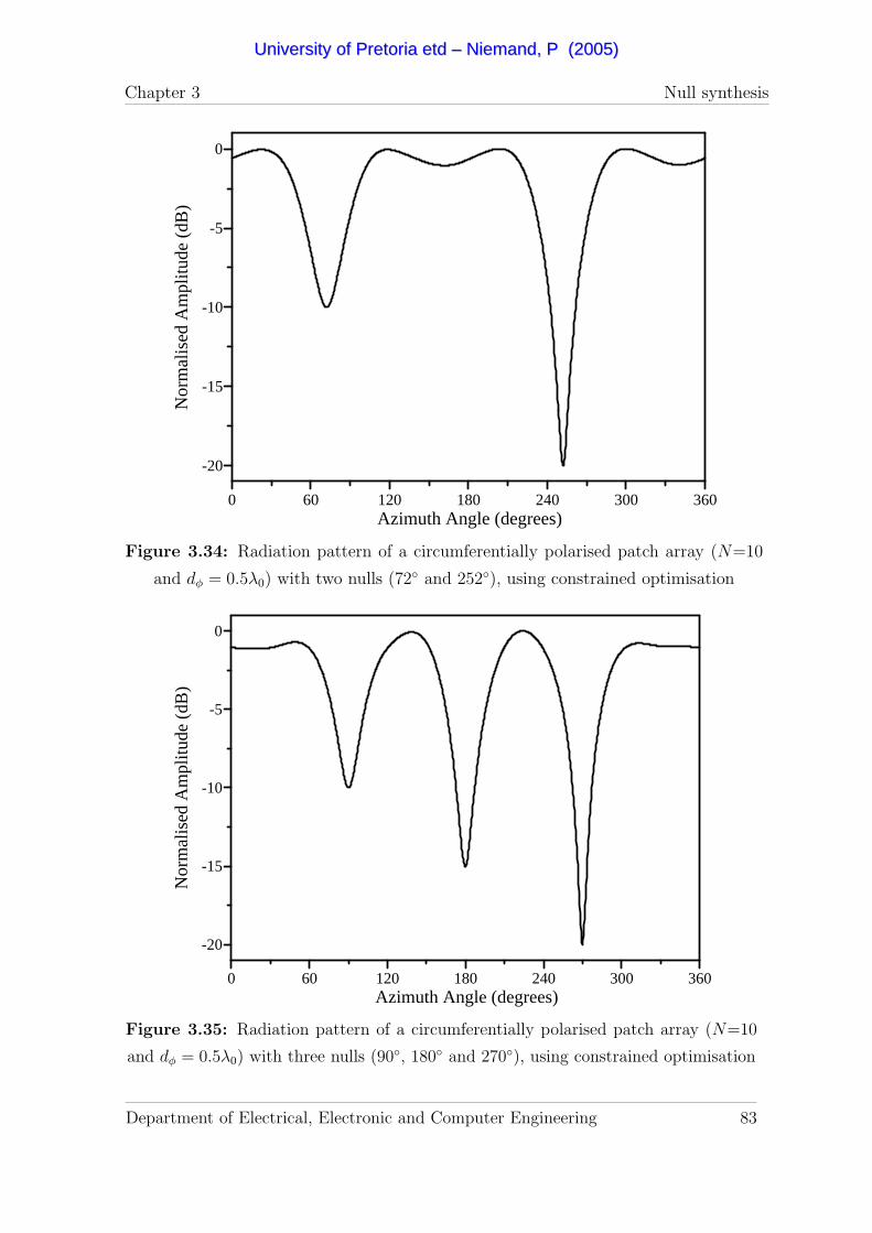
Chapter 3 Null synthesis
-20
-15
-10
-5
0
Nor
mal
ised
Am
plitu
d e (
dB)
0 60 120 180 240 300 360Azimuth Angle (degrees)
Figure 3.34: Radiation pattern of a circumferentially polarised patch array (N=10
and dφ = 0.5λ0) with two nulls (72 and 252), using constrained optimisation
-20
-15
-10
-5
0
Nor
mal
ised
Am
plitu
d e (
dB)
0 60 120 180 240 300 360Azimuth Angle (degrees)
Figure 3.35: Radiation pattern of a circumferentially polarised patch array (N=10
and dφ = 0.5λ0) with three nulls (90, 180 and 270), using constrained optimisation
Department of Electrical, Electronic and Computer Engineering 83
UUnniivveerrssiittyy ooff PPrreettoorriiaa eettdd –– NNiieemmaanndd,, PP ((22000055))

Chapter 3 Null synthesis
3.6 Influences of the antenna element characteris-
tics
The characteristics of the resulting null pattern may be influenced by the characteristics
of the array as well as the attributes of the antenna element. The influence of the array
characteristics such as the number of elements and the inter-element spacing have been
shown in Section 3.3.1. Since the antenna element pattern varies with the height of
the patch and the dielectric constant of the substrate, the resulting null pattern may
also change due to variations in these characteristics. Different patch antenna elements
were used to study the effects of element characteristics on the resulting null pattern.
3.6.1 Influence of the dielectric constant
Three different cylindrical patch antennas were designed to study the influence of using
substrates with different dielectric constants. All three patches were designed for a
resonant frequency of 1.8 GHz for the dominant mode and had a substrate height of
h = 1.6 cm. For the first patch antenna, air was used as the substrate (εr = 1). The
dimensions were L = 7.97 cm and W = 8.2 cm for the axial polarisation and vice versa
for the circumferential polarisation. A substrate with εr = 4.4 was used to design the
second patch antenna with dimensions of L = 3.87 cm and W = 4.75 cm for the axial
polarisation; for the circumferential polarisation W = 3.87 cm and L = 4.75 cm. The
results using these two patch antenna elements were compared with the results in the
previous sections using the patch antenna with εr = 2.3 (L = 5.44 cm and W = 6 cm).
An omnidirectional pattern with a single null of -40 dB at 180 was specified. In each
case the orthogonal base was modified to include the radiation pattern of the specific
patch antenna element. Firstly, the constrained optimisation method was used without
constraining the gain ripple. Figures 3.36 and 3.37 compare the amplitudes of result-
ing radiation patterns for the circumferential and axial polarisation, respectively. The
axially polarised array using the air substrate forms the widest null with the most gain
ripple. The other two axially polarised arrays form nulls with similar characteristics.
The null width is almost the same for all three axial polarisation cases. For the cir-
cumferential polarisation, the resulting pattern of the array using the substrate with
εr = 4.4 has the highest gain ripple. The null widths of all three patterns differ by less
Department of Electrical, Electronic and Computer Engineering 84
UUnniivveerrssiittyy ooff PPrreettoorriiaa eettdd –– NNiieemmaanndd,, PP ((22000055))

Chapter 3 Null synthesis
than 0.5.
The ripple was also constrained (1 dB or less) to yield the resulting patterns in Fig-
ures 3.38 and 3.39 for the circumferential and axial polarisation, respectively. In the
circumferential and axial polarisations, the air substrate array produces the widest and
narrowest nulls, respectively. On the other hand, the array with the εr = 4.4 substrate,
yields the narrowest and widest nulls in the circumferential and axial polarisations, re-
spectively. From these results, it can be concluded that the choice of the dielectric
constant of the substrate will have an effect on the resulting null pattern character-
istics. This is mainly due to the differences in element patterns when using different
substrates.
3.6.2 Influence of the height of the substrate
Another attribute of the patch antenna elements which modifies the element pattern,
is the height of the substrate. Two patch antenna elements with different heights
were used to illustrate the influence of the height of the substrate. A foam based
substrate with εr = 1.024 was used to design the two patches with h = 1.6 mm and
h = 5 mm, respectively. Both patches were designed for a resonant frequency of
1.8 GHz. The dimensions for both patches were L = 7.36 cm and W = 7.6 cm for the
axial polarisation and vice versa for the circumferential polarisation. The cavity model
was used to obtain the element pattern of the patch with h = 1.6 mm. For the patch
with h = 5 mm, a FDTD software package [101] was used to compute the element
pattern.
The constrained optimisation method was used to determine the excitation vectors for
a -40 dB null at 180. Figures 3.40 and 3.41 compare the amplitude of the resulting
radiated fields when only the null depth is constrained for the circumferential and
axial polarisations, respectively. For h = 5 mm, a wider null with a higher gain
ripple is formed for the circumferential polarisation. In contrast, the results are very
similar when the two axial polarisation patterns are compared. When the gain ripple
is constrained to 1dB or less, the resulting amplitude pattern in Figures 3.42 and 3.43
are obtained for the circumferential and axial polarisations, respectively.
Department of Electrical, Electronic and Computer Engineering 85
UUnniivveerrssiittyy ooff PPrreettoorriiaa eettdd –– NNiieemmaanndd,, PP ((22000055))
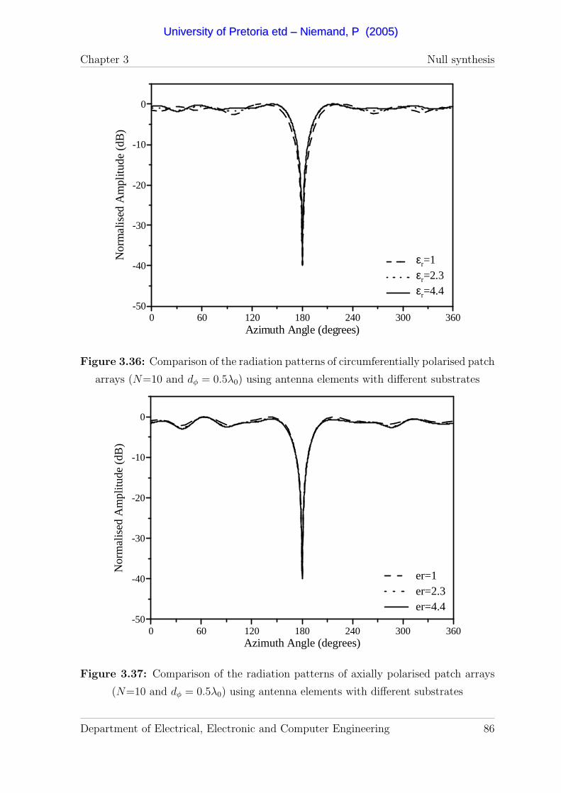
Chapter 3 Null synthesis
-50
-40
-30
-20
-10
0
Nor
mal
ised
Am
plitu
de (
dB)
0 60 120 180 240 300 360Azimuth Angle (degrees)
er=1er=2.3er=4.4
εr=1εr=2.3εr=4.4
Figure 3.36: Comparison of the radiation patterns of circumferentially polarised patch
arrays (N=10 and dφ = 0.5λ0) using antenna elements with different substrates
-50
-40
-30
-20
-10
0
Nor
mal
ised
Am
plitu
de (
dB)
0 60 120 180 240 300 360Azimuth Angle (degrees)
er=1er=2.3er=4.4
Figure 3.37: Comparison of the radiation patterns of axially polarised patch arrays
(N=10 and dφ = 0.5λ0) using antenna elements with different substrates
Department of Electrical, Electronic and Computer Engineering 86
UUnniivveerrssiittyy ooff PPrreettoorriiaa eettdd –– NNiieemmaanndd,, PP ((22000055))

Chapter 3 Null synthesis
-50
-40
-30
-20
-10
0
Nor
mal
ised
Am
plitu
de (
dB)
0 60 120 180 240 300 360Azimuth Angle (degrees)
er=1er=2.3er=4.4
Figure 3.38: Comparison of the radiation patterns of circumferentially polarised patch
arrays (N=10 and dφ = 0.5λ0) using antenna elements with different substrates
-50
-40
-30
-20
-10
0
Nor
mal
ised
Am
plitu
de (
dB)
0 60 120 180 240 300 360Azimuth Angle (degrees)
er=1er=2.3er=4.4
Figure 3.39: Comparison of the radiation patterns of axially polarised patch arrays
(N=10 and dφ = 0.5λ0) using antenna elements with different substrates
Department of Electrical, Electronic and Computer Engineering 87
UUnniivveerrssiittyy ooff PPrreettoorriiaa eettdd –– NNiieemmaanndd,, PP ((22000055))
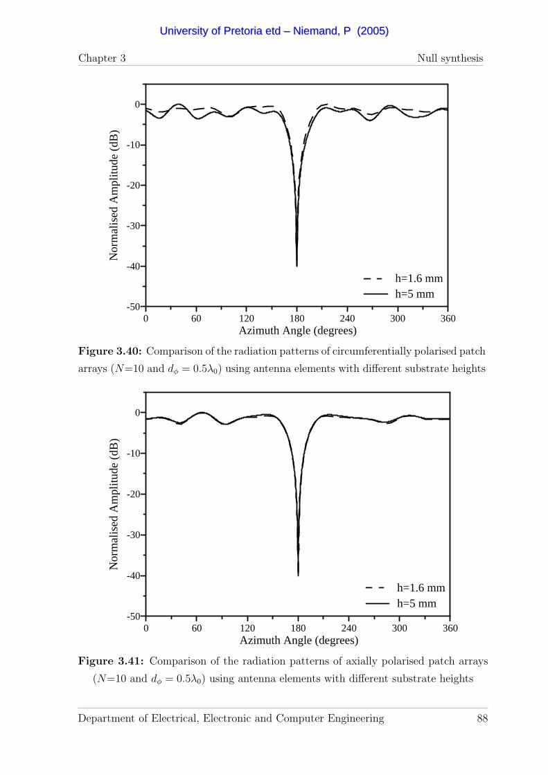
Chapter 3 Null synthesis
-50
-40
-30
-20
-10
0N
orm
alis
ed A
mpl
itud e
(dB
)
0 60 120 180 240 300 360Azimuth Angle (degrees)
h=1.6 mmh=5 mm
Figure 3.40: Comparison of the radiation patterns of circumferentially polarised patch
arrays (N=10 and dφ = 0.5λ0) using antenna elements with different substrate heights
-50
-40
-30
-20
-10
0
Nor
mal
ised
Am
plitu
d e (
dB)
0 60 120 180 240 300 360Azimuth Angle (degrees)
h=1.6 mmh=5 mm
Figure 3.41: Comparison of the radiation patterns of axially polarised patch arrays
(N=10 and dφ = 0.5λ0) using antenna elements with different substrate heights
Department of Electrical, Electronic and Computer Engineering 88
UUnniivveerrssiittyy ooff PPrreettoorriiaa eettdd –– NNiieemmaanndd,, PP ((22000055))
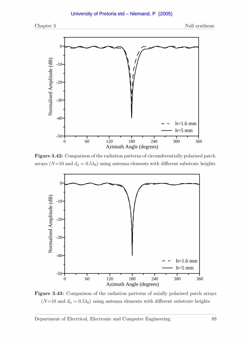
Chapter 3 Null synthesis
-50
-40
-30
-20
-10
0N
orm
alis
ed A
mpl
itud e
(dB
)
0 60 120 180 240 300 360Azimuth Angle (degrees)
h=1.6 mmh=5 mm
Figure 3.42: Comparison of the radiation patterns of circumferentially polarised patch
arrays (N=10 and dφ = 0.5λ0) using antenna elements with different substrate heights
-50
-40
-30
-20
-10
0
Nor
mal
ised
Am
plitu
d e (
dB)
0 60 120 180 240 300 360Azimuth Angle (degrees)
h=1.6 mmh=5 mm
Figure 3.43: Comparison of the radiation patterns of axially polarised patch arrays
(N=10 and dφ = 0.5λ0) using antenna elements with different substrate heights
Department of Electrical, Electronic and Computer Engineering 89
UUnniivveerrssiittyy ooff PPrreettoorriiaa eettdd –– NNiieemmaanndd,, PP ((22000055))
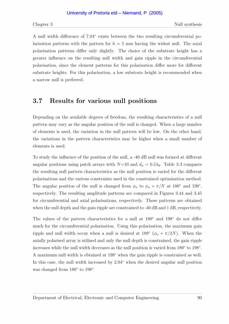
Chapter 3 Null synthesis
A null width difference of 7.04 exists between the two resulting circumferential po-
larisation patterns with the pattern for h = 5 mm having the widest null. The axial
polarisation patterns differ only slightly. The choice of the substrate height has a
greater influence on the resulting null width and gain ripple in the circumferential
polarisation, since the element patterns for this polarisation differ more for different
substrate heights. For this polarisation, a low substrate height is recommended when
a narrow null is preferred.
3.7 Results for various null positions
Depending on the available degrees of freedom, the resulting characteristics of a null
pattern may vary as the angular position of the null is changed. When a large number
of elements is used, the variation in the null pattern will be low. On the other hand,
the variations in the pattern characteristics may be higher when a small number of
elements is used.
To study the influence of the position of the null, a -40 dB null was formed at different
angular positions using patch arrays with N=10 and dφ = 0.5λ0. Table 3.3 compares
the resulting null pattern characteristics as the null position is varied for the different
polarisations and the various constraints used in the constrained optimisation method.
The angular position of the null is changed from φn to φn + π/N at 180 and 198,
respectively. The resulting amplitude patterns are compared in Figures 3.44 and 3.45
for circumferential and axial polarisations, respectively. These patterns are obtained
when the null depth and the gain ripple are constrained to -40 dB and 1 dB, respectively.
The values of the pattern characteristics for a null at 180 and 198 do not differ
much for the circumferential polarisation. Using this polarisation, the maximum gain
ripple and null width occur when a null is desired at 189 (φn + π/2N). When the
axially polarised array is utilised and only the null depth is constrained, the gain ripple
increases while the null width decreases as the null position is varied from 180 to 198.
A maximum null width is obtained at 198 when the gain ripple is constrained as well.
In this case, the null width increased by 2.04 when the desired angular null position
was changed from 180 to 198.
Department of Electrical, Electronic and Computer Engineering 90
UUnniivveerrssiittyy ooff PPrreettoorriiaa eettdd –– NNiieemmaanndd,, PP ((22000055))
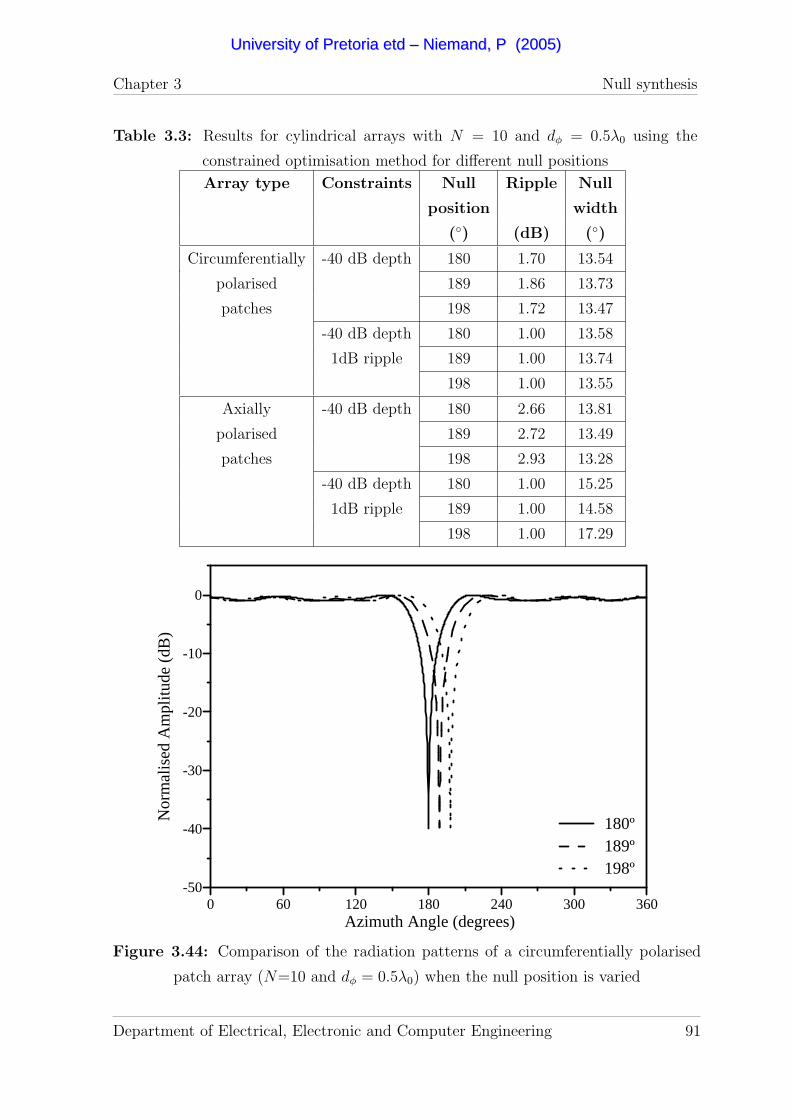
Chapter 3 Null synthesis
Table 3.3: Results for cylindrical arrays with N = 10 and dφ = 0.5λ0 using the
constrained optimisation method for different null positions
Array type Constraints Null Ripple Null
position width
() (dB) ()
Circumferentially -40 dB depth 180 1.70 13.54
polarised 189 1.86 13.73
patches 198 1.72 13.47
-40 dB depth 180 1.00 13.58
1dB ripple 189 1.00 13.74
198 1.00 13.55
Axially -40 dB depth 180 2.66 13.81
polarised 189 2.72 13.49
patches 198 2.93 13.28
-40 dB depth 180 1.00 15.25
1dB ripple 189 1.00 14.58
198 1.00 17.29
-50
-40
-30
-20
-10
0
Nor
mal
ised
Am
plitu
d e (
dB)
0 60 120 180 240 300 360Azimuth Angle (degrees)
180º189º198º
Figure 3.44: Comparison of the radiation patterns of a circumferentially polarised
patch array (N=10 and dφ = 0.5λ0) when the null position is varied
Department of Electrical, Electronic and Computer Engineering 91
UUnniivveerrssiittyy ooff PPrreettoorriiaa eettdd –– NNiieemmaanndd,, PP ((22000055))

Chapter 3 Null synthesis
-50
-40
-30
-20
-10
0N
orm
alis
ed A
mpl
itud e
(dB
)
0 60 120 180 240 300 360Azimuth Angle (degrees)
180º189º198º
Figure 3.45: Comparison of the radiation patterns of an axially polarised patch array
(N=10 and dφ = 0.5λ0) when the null position is varied
The degree to which the characteristics of the resulting null pattern change as the null
position is varied, depends on the utilised polarisation. The variations in the pattern
characteristics consequently depend on the element pattern that is incorporated. By
carefull selection of the element pattern, the sensitivity of the pattern characteristics
to a change in the null position, can thus be minimised.
3.8 Summary
Abele et al. [53] introduced a null synthesis technique for a cylindrical dipole array.
The technique utilised the orthogonal projection method and projected an idealised
null pattern onto the orthogonal base of realisable array patterns. The resulting array
pattern was an omni-directional pattern with one or more nulls. Vescovo [56] extended
the orthogonal projection method for an arc array with theoretical directional elements.
A beam pattern was formed through the projection method and additional nulls were
introduced in the pattern with null constraints to reduce the side lobe level. In this
chapter the null synthesis technique of Abele was extended to incorporate the radiation
Department of Electrical, Electronic and Computer Engineering 92
UUnniivveerrssiittyy ooff PPrreettoorriiaa eettdd –– NNiieemmaanndd,, PP ((22000055))
Chapter 3 Null synthesis
patterns of conformal microstrip patches.
In this chapter, the null synthesis technique of Abele [53] was used to form an omnidi-
rectional radiation pattern with nulls at specified locations for a cylindrical microstrip
patch array. The orthogonal projection method was extended by modifying the or-
thogonal base for the space of realisable array pattern to include the radiation pattern
characteristics of microstrip patch antennae mounted on a conducting cylinder. For
electrically thin patches, the cavity model was used to compute the element pattern
of the cylindrical patches. A FDTD software package [101] was used to calculate the
element pattern of electrically thick cylindrical patches. The unconstrained optimum
element excitations obtained from the orthogonal projection method provided an op-
timal array pattern with the minimum pattern error (in a least square sense).
The resulting radiation pattern contained the desired null at the specified angular
location in the otherwise omnidirectional pattern. By applying a Hamming window to
the sequence excitations before the element excitations are computed, the gain ripple
in the omniregion was reduced. The resulting null pattern characteristics were also
influenced by the array configuration parameters such as the number of elements and
the inter-element spacing. When an infinitely deep null was desired, the resulting
gain ripple and null width gradually decreased while the null depth increases as the
number of elements were increased for both axially and circumferentially polarised
microstrip patch arrays. As the inter-element spacing was increased, the gain ripple
and null width increased as well. For a large number of elements the yielded null widths
became comparable to the null widths obtained with dipoles as the array elements. In
most cases, the microstrip patches yielded better gain ripple due to the high level of
gain ripple in the radiated field of cylindrical dipole arrays.
Since the amplitude and phase of the radiation pattern were optimised simultaneously,
the optimal array pattern may not have had the desired characteristics. Although
the ripple was successfully decreased by using the windowing function, the result-
ing null width was increased. Instead of only minimising the array pattern error, a
multi-objective optimisation approach was followed [95–97]. The Objective Weight-
ing method, previously applied in other fields of computational electromagnetic prob-
lems [96, 97], was used to improve the amplitude pattern characteristics. A global
performance function was defined by utilising both the amplitude pattern error and
the phase pattern error. The optimisation problem was solved by finding the critical
Department of Electrical, Electronic and Computer Engineering 93
UUnniivveerrssiittyy ooff PPrreettoorriiaa eettdd –– NNiieemmaanndd,, PP ((22000055))
Chapter 3 Null synthesis
ratio of the weights that were assigned to the two errors in the performance function.
Each performance function was minimised by using an unconstrained minimisation al-
gorithm [99]. The excitation vector obtained from the orthogonal projection method
yielded an optimum radiation pattern with the minimum pattern error and was there-
fore chosen as the starting vector. The resulting excitation vector that minimised
the performance function formed with the critical weight ratio, was used to form the
radiation pattern.
Compared to the results of the windowing method, the objective weighting method
provided a null pattern with a narrower and deeper null and with a higher gain ripple in
the omni-region. An increase in the phase pattern error was observed due to the trade-
off that existed between the two pattern errors in the performance function. When
infinitely deep nulls were desired, the method could synthesise deep nulls utilising only
a small number of elements.
Constrained optimisation methods have been used previously to form beam patterns
with cylindrical arrays [45, 52, 56]. Prasad [45] applied the least squares optimisation
method to circular and arc arrays to form a beam pattern with a specified beamwidth.
Additional nulls were also placed in the sidelobe region by using null constraints while
minimising the mean square difference between the desired pattern and the optimum
pattern. The Hook and Jeeves algorithm was also used to perform an iterative search
to find the optimum excitation vector while satisfying the null constraints. During the
search, the sidelobe level was minimised. Ares et al. [52] used a simulated annealing
technique to produce beam patterns for a circular arc array on a cylinder. A cost
function, which could include terms to control the radiation pattern, was minimised.
Terms which placed constraints on the excitations, could also be included in the cost
function. The sidelobe level was also decreased by placing null constraints in the
region near the main lobe [56]. In this chapter, constrained optimisation was also used
to yield an excitation vector which minimises the pattern error under the constraints
specified for the different amplitude pattern characteristics. The minimum pattern
error was found using a constrained minimisation algorithm [99]. The optimum element
excitation vector, which was obtained from the projection method, was used as the
starting vector.
Individual characteristics as well as combinations of characteristics were controlled
using the constrained optimisation. Compared to the above methods, the constrained
Department of Electrical, Electronic and Computer Engineering 94
UUnniivveerrssiittyy ooff PPrreettoorriiaa eettdd –– NNiieemmaanndd,, PP ((22000055))
Chapter 3 Null synthesis
optimisation algorithm obtained a null width close to the null width resulting from the
objective weighting method, while controlling both the null depth and gain ripple in the
omni-region. The method was also able to form multiple nulls with different null depths
while constraining the gain ripple. Due to the control provided by the algorithm, the
resulting pattern characteristics could be made independent of the number of elements
and the inter-element spacing.
Since the element pattern can not be factorised out of the array factor, any change in
the element pattern may influence the characteristics of the resulting array pattern.
While controlling certain null pattern characteristics, the influence of changes in the
antenna element configuration on the remaining unconstrained pattern characteristics,
was studied. The effects of the changes in the dielectric constant and the height of
the substrate are different for the circumferentially and axially polarisations. The null
pattern characteristics for the axial polarisation are only slightly influenced by a change
in substrate height. When the null depth is constrained, the resulting ripple and null
width for both polarisations are influenced by a change in the dielectric constant. The
degree to which the unconstrained characteristics of the resulting null pattern change
as the null position is varied, also depend on the utilised polarisation. The sensitivity
of the resulting null pattern characteristics to a change in the desired null position
or an antenna element characteristic, can be minimised by a careful selection of the
element pattern.
The above three null synthesis methods determines the necessary element excitations
without considering the mutual coupling between the elements. If the inter-element
spacing is chosen large enough or the height of the patch elements is low in terms
of wavelength, the mutual coupling factor is small and has very little effect on the
resulting pattern. On the other hand, the mutual coupling between closely spaced
patch antenna elements with high substrate heights, is large enough to distort the
resulting radiation pattern. Consequently, the mutual coupling must be compensated
for. In most systems, the driving impedances of the patch antenna elements also
need to be matched to the input system. In the next chapter, a mutual coupling
compensation technique is employed which alter the patch antenna element geometries
to simultaneously correct the resulting null pattern and the driving impedances of the
antenna elements.
Department of Electrical, Electronic and Computer Engineering 95
UUnniivveerrssiittyy ooff PPrreettoorriiaa eettdd –– NNiieemmaanndd,, PP ((22000055))
CHAPTER 4
IMPLEMENTATION OF
CYLINDRICAL MICROSTRIP
PATCH ARRAYS
The null synthesis techniques proposed in the previous chapter do not consider the
mutual coupling between the antenna elements and it is also assumed that the antenna
elements do not disturb each other’s current distributions. Each element’s radiation
pattern is thus considered to be identical to the radiation pattern of an isolated antenna
in both shape and radiation strength. The input impedance of each antenna element
is furthermore assumed to be matched to the impedance of its port in the feeding
network.
These assumptions are valid when large inter-element spacings and low substrate
heights are used to minimise the effects of the mutual coupling. In Chapter 3, it
was seen that the utilisation of large inter-element spacings leads to wide nulls with
high gain ripple in the omni-region. The use of a low substrate height is also not
favoured since it decreases the realisable bandwidth. Small inter-element spacings and
higher substrate heights are therefore preferred to yield null patterns with a reasonable
bandwidth within the pattern specifications.
When small inter-element spacings are used, distortion of the excitations may occur due
to the mutual coupling. The desired radiation pattern is consequently deteriorated due
to the errors in the element excitations [72,73]. During null synthesis, these erroneous
96
UUnniivveerrssiittyy ooff PPrreettoorriiaa eettdd –– NNiieemmaanndd,, PP ((22000055))
Chapter 4 Implementation of cylindrical microstrip patch arrays
excitations lead to null filling and null position errors [53, 74]. The nulls introduced
in the beam patterns of linear monopole arrays were found to be shifted or filled due
to the mutual coupling [74]. Abele [54] studied the effect of the mutual coupling on
the null pattern of a cylindrical dipole array and found that the coupling needed to be
compensated for to prevent distortion of the null characteristics.
In this chapter, an investigation into the extent to which the mutual coupling has
an influence on the null pattern of a cylindrical microstrip patch array will be done.
When it is established that the mutual coupling may not be neglected for a specific
array configuration and null pattern, a technique to compensate for the mutual coupling
will be needed.
Yang et al [86] proposed a mutual coupling compensation technique to obtain the de-
sired bandwidth and voltage standing wave ratio (VSWR) at the resonant frequency
for an electromagnetically coupled (EMC) dipole antenna array. For a given set of exci-
tation voltages, the dipole lengths and dipole offsets from the microstrip feed line were
altered to obtain the prescribed driving admittances seen by the feed lines. As a result,
a good similarity was also found between the desired and measured radiation patterns.
Chen et al proposed a similar technique for a linear array of parallel dipoles [88]. The
lengths and the radii of the dipoles were changed to obtain equal driving impedances
for all the dipoles. Consequently, the desired radiation pattern was obtained. In this
chapter, the mutual coupling compensation technique is applied to both linear and
cylindrical microstrip patch arrays.
In the first section, the design of a cylindrical microstrip patch element for both po-
larisations will be discussed. The effect of the mutual coupling on the bandwidth
of a linear microstrip patch array will be investigated firstly. This investigation was
conducted in order to study the improvement in the bandwidth due to the use of
the mutual coupling compensation technique. Afterwards, the effect of coupling on
the array imbedded element pattern of the cylindrical microstrip patch element will
be shown. The influence of the mutual coupling on the null pattern of a cylindrical
microstrip patch will also be investigated for various inter-element spacings and both
polarisations. The mutual coupling compensation technique will be used for both the
linear and cylindrical microstrip patch arrays. The improvement in the characteristics
of the linear and cylindrical patch arrays due to the compensation technique will be
discussed using two test cases.
Department of Electrical, Electronic and Computer Engineering 97
UUnniivveerrssiittyy ooff PPrreettoorriiaa eettdd –– NNiieemmaanndd,, PP ((22000055))
Chapter 4 Implementation of cylindrical microstrip patch arrays
4.1 Design of cylindrical microstrip patch element
In the investigation of the cylindrical microstrip patch arrays, probe-fed microstrip
patches were also utilised as the array elements. To assist with the design of the
array elements, a commercial electromagnetic software package which apply the Finite
Difference Time Domain (FDTD) method [101], was used. To verify the results of the
software package, a single element was designed, manufactured and measured. The
measured results were then compared with the simulated results.
Figure 4.1 illustrates the cylindrical microstrip patch element (axially polarised) on a
copper cylinder, as well as the probe feeding mechanism. The patch element consisted
of a 5mm layer of air, a thin layer of FR4 (εr = 4.17) and a 36 µm layer of copper.
The patch was etched onto the thin layer of FR4 (with a thickness of 0.127mm) and
conformally shaped to the patch along the surface of the cylinder.
The FDTD software package uses conforming cell elements in the xy-plane, and rect-
angular cell elements in the xz- and yz-planes. To make use of the conforming cells, the
axes of the cylinder were thus aligned with the z-axis. The three main considerations
during the design of the single element using the software, were the simulation of the
probe feeding, the thin layer of copper and the thin layer of FR4.
When the thin layers of FR4 and copper were used in the simulation, a very large
number of cells was generated during the meshing of the problem. This high number
of cells exceeded the simulation capability of the software and an alternative method for
the simulation of the problem was thus needed. The effect of the thin layer of FR4 was
simulated by combining the layers of air and FR4 into one layer. The characteristics
of the combined layer were found by simulating and comparing the input impedances
of a planar patch with the two layers and a planar patch with a combined layer. A
single layer with a height of 4.77mm and εr = 1.0705 were found to yield similar results
compared to the double layer. The thickness of the copper layer was increased to 1mm
in order to reduce the number of cells.
The probe-feed was simulated using a square co-axial probe. The dimensions of the
probe-feed were designed for S11 = S22 = 0 and S12 = S21 = 1. The resulting centre
conductor had a diameter of 0.8mm. The outer conductor had an outer diameter of
4mm and a thickness of 0.45mm. The dielectric material in the coax had an εr of 2.3.
Department of Electrical, Electronic and Computer Engineering 98
UUnniivveerrssiittyy ooff PPrreettoorriiaa eettdd –– NNiieemmaanndd,, PP ((22000055))
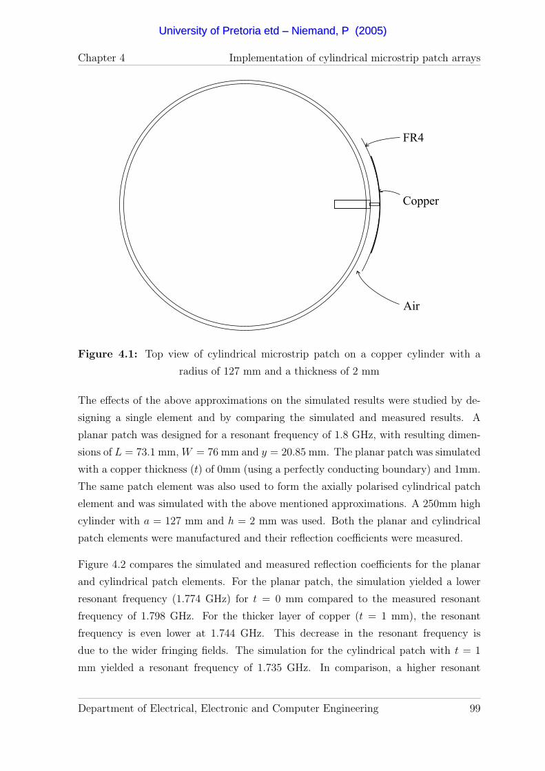
Chapter 4 Implementation of cylindrical microstrip patch arrays
FR4
Copper
Air
Figure 4.1: Top view of cylindrical microstrip patch on a copper cylinder with a
radius of 127 mm and a thickness of 2 mm
The effects of the above approximations on the simulated results were studied by de-
signing a single element and by comparing the simulated and measured results. A
planar patch was designed for a resonant frequency of 1.8 GHz, with resulting dimen-
sions of L = 73.1 mm, W = 76 mm and y = 20.85 mm. The planar patch was simulated
with a copper thickness (t) of 0mm (using a perfectly conducting boundary) and 1mm.
The same patch element was also used to form the axially polarised cylindrical patch
element and was simulated with the above mentioned approximations. A 250mm high
cylinder with a = 127 mm and h = 2 mm was used. Both the planar and cylindrical
patch elements were manufactured and their reflection coefficients were measured.
Figure 4.2 compares the simulated and measured reflection coefficients for the planar
and cylindrical patch elements. For the planar patch, the simulation yielded a lower
resonant frequency (1.774 GHz) for t = 0 mm compared to the measured resonant
frequency of 1.798 GHz. For the thicker layer of copper (t = 1 mm), the resonant
frequency is even lower at 1.744 GHz. This decrease in the resonant frequency is
due to the wider fringing fields. The simulation for the cylindrical patch with t = 1
mm yielded a resonant frequency of 1.735 GHz. In comparison, a higher resonant
Department of Electrical, Electronic and Computer Engineering 99
UUnniivveerrssiittyy ooff PPrreettoorriiaa eettdd –– NNiieemmaanndd,, PP ((22000055))
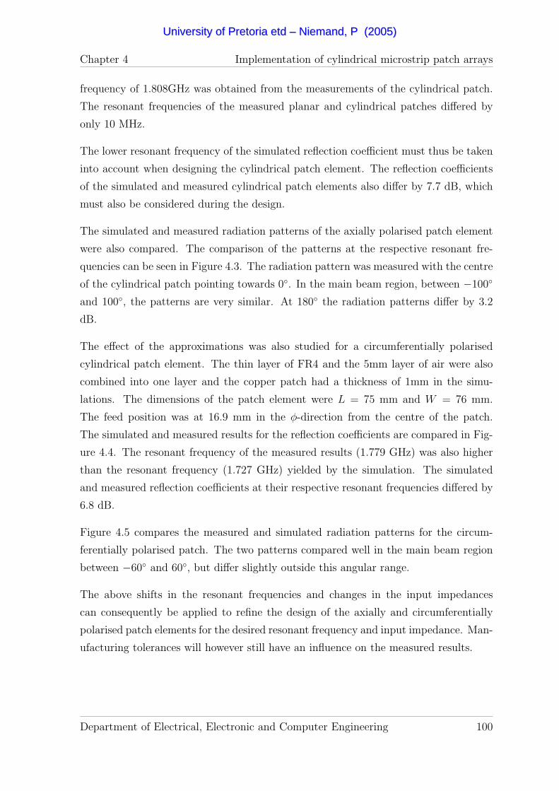
Chapter 4 Implementation of cylindrical microstrip patch arrays
frequency of 1.808GHz was obtained from the measurements of the cylindrical patch.
The resonant frequencies of the measured planar and cylindrical patches differed by
only 10 MHz.
The lower resonant frequency of the simulated reflection coefficient must thus be taken
into account when designing the cylindrical patch element. The reflection coefficients
of the simulated and measured cylindrical patch elements also differ by 7.7 dB, which
must also be considered during the design.
The simulated and measured radiation patterns of the axially polarised patch element
were also compared. The comparison of the patterns at the respective resonant fre-
quencies can be seen in Figure 4.3. The radiation pattern was measured with the centre
of the cylindrical patch pointing towards 0. In the main beam region, between −100
and 100, the patterns are very similar. At 180 the radiation patterns differ by 3.2
dB.
The effect of the approximations was also studied for a circumferentially polarised
cylindrical patch element. The thin layer of FR4 and the 5mm layer of air were also
combined into one layer and the copper patch had a thickness of 1mm in the simu-
lations. The dimensions of the patch element were L = 75 mm and W = 76 mm.
The feed position was at 16.9 mm in the φ-direction from the centre of the patch.
The simulated and measured results for the reflection coefficients are compared in Fig-
ure 4.4. The resonant frequency of the measured results (1.779 GHz) was also higher
than the resonant frequency (1.727 GHz) yielded by the simulation. The simulated
and measured reflection coefficients at their respective resonant frequencies differed by
6.8 dB.
Figure 4.5 compares the measured and simulated radiation patterns for the circum-
ferentially polarised patch. The two patterns compared well in the main beam region
between −60 and 60, but differ slightly outside this angular range.
The above shifts in the resonant frequencies and changes in the input impedances
can consequently be applied to refine the design of the axially and circumferentially
polarised patch elements for the desired resonant frequency and input impedance. Man-
ufacturing tolerances will however still have an influence on the measured results.
Department of Electrical, Electronic and Computer Engineering 100
UUnniivveerrssiittyy ooff PPrreettoorriiaa eettdd –– NNiieemmaanndd,, PP ((22000055))
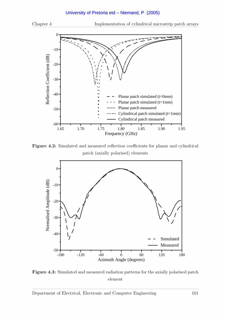
Chapter 4 Implementation of cylindrical microstrip patch arrays
-60
-50
-40
-30
-20
-10
0
Ref
lect
ion
Coe
ffic
ient
(dB
)
1.65 1.70 1.75 1.80 1.85 1.90 1.95Frequency (GHz)
Planar patch simulated (t=0mm)Planar patch simulated (t=1mm)Planar patch measuredCylindrical patch simulated (t=1mm)Cylindrical patch measured
Figure 4.2: Simulated and measured reflection coefficients for planar and cylindrical
patch (axially polarised) elements
-50
-40
-30
-20
-10
0
Nor
mal
ised
Am
plitu
de (
dB)
-180 -120 -60 0 60 120 180Azimuth Angle (degrees)
SimulatedMeasured
Figure 4.3: Simulated and measured radiation patterns for the axially polarised patch
element
Department of Electrical, Electronic and Computer Engineering 101
UUnniivveerrssiittyy ooff PPrreettoorriiaa eettdd –– NNiieemmaanndd,, PP ((22000055))

Chapter 4 Implementation of cylindrical microstrip patch arrays
-40
-30
-20
-10
0
Ref
lect
ion
Coe
ffic
ient
(dB
)
1.65 1.70 1.75 1.80 1.85 1.90 1.95Frequency (GHz)
SimulatedMeasured
Figure 4.4: Simulated and measured reflection coefficients for the circumferentially
polarised patch element
-50
-40
-30
-20
-10
0
Nor
mal
ised
Am
plitu
de (
dB)
-180 -120 -60 0 60 120 180Azimuth Angle (degrees)
SimulatedMeasured
Figure 4.5: Simulated and measured radiation patterns for the circumferentially po-
larised patch element
Department of Electrical, Electronic and Computer Engineering 102
UUnniivveerrssiittyy ooff PPrreettoorriiaa eettdd –– NNiieemmaanndd,, PP ((22000055))
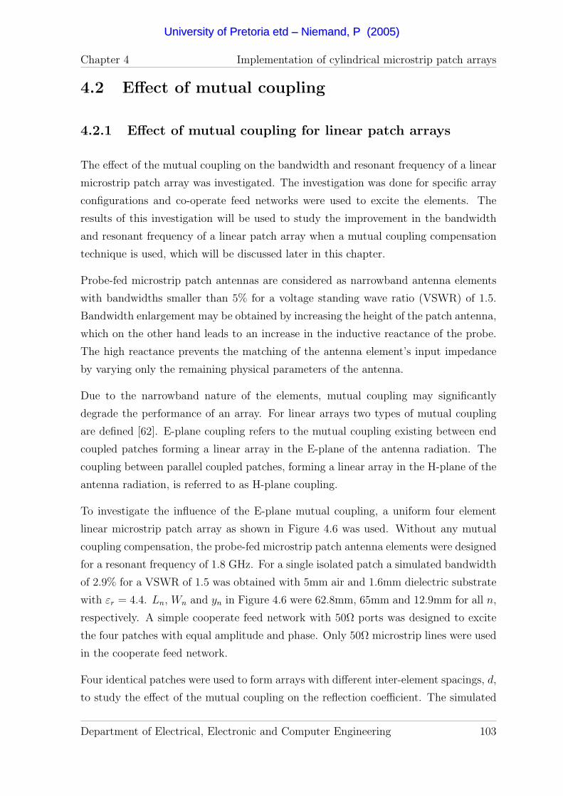
Chapter 4 Implementation of cylindrical microstrip patch arrays
4.2 Effect of mutual coupling
4.2.1 Effect of mutual coupling for linear patch arrays
The effect of the mutual coupling on the bandwidth and resonant frequency of a linear
microstrip patch array was investigated. The investigation was done for specific array
configurations and co-operate feed networks were used to excite the elements. The
results of this investigation will be used to study the improvement in the bandwidth
and resonant frequency of a linear patch array when a mutual coupling compensation
technique is used, which will be discussed later in this chapter.
Probe-fed microstrip patch antennas are considered as narrowband antenna elements
with bandwidths smaller than 5% for a voltage standing wave ratio (VSWR) of 1.5.
Bandwidth enlargement may be obtained by increasing the height of the patch antenna,
which on the other hand leads to an increase in the inductive reactance of the probe.
The high reactance prevents the matching of the antenna element’s input impedance
by varying only the remaining physical parameters of the antenna.
Due to the narrowband nature of the elements, mutual coupling may significantly
degrade the performance of an array. For linear arrays two types of mutual coupling
are defined [62]. E-plane coupling refers to the mutual coupling existing between end
coupled patches forming a linear array in the E-plane of the antenna radiation. The
coupling between parallel coupled patches, forming a linear array in the H-plane of the
antenna radiation, is referred to as H-plane coupling.
To investigate the influence of the E-plane mutual coupling, a uniform four element
linear microstrip patch array as shown in Figure 4.6 was used. Without any mutual
coupling compensation, the probe-fed microstrip patch antenna elements were designed
for a resonant frequency of 1.8 GHz. For a single isolated patch a simulated bandwidth
of 2.9% for a VSWR of 1.5 was obtained with 5mm air and 1.6mm dielectric substrate
with εr = 4.4. Ln, Wn and yn in Figure 4.6 were 62.8mm, 65mm and 12.9mm for all n,
respectively. A simple cooperate feed network with 50Ω ports was designed to excite
the four patches with equal amplitude and phase. Only 50Ω microstrip lines were used
in the cooperate feed network.
Four identical patches were used to form arrays with different inter-element spacings, d,
to study the effect of the mutual coupling on the reflection coefficient. The simulated
Department of Electrical, Electronic and Computer Engineering 103
UUnniivveerrssiittyy ooff PPrreettoorriiaa eettdd –– NNiieemmaanndd,, PP ((22000055))

Chapter 4 Implementation of cylindrical microstrip patch arrays
(a)
(b)
Figure 4.6: Four element linear microstrip patch array: (a) Top view, (b) Side view
reflection coefficients at the input ports of the feeding networks for the arrays with
different inter-element spacings are shown in Figure 4.7. It is seen that both the
minimum of the reflection coefficient and the resonant frequency are influenced by the
mutual coupling. For d = 0.5λ0, the resonant frequency shifted by 2.8%, which is
close to the bandwidth of an isolated patch. In this case, there is also no measurable
bandwidth for a VSWR of 1.5. As the inter-element spacing increases, the coupling
between the antenna elements decreases and has less effect on the bandwidth and
resonant frequency. Table 4.1 summarises the magnitude of the E-plane coupling and
the resulting characteristics for the different inter-element spacings. The tabulated
coupling is the coupling between two neighbouring patch antennae.
The effect of H-plane mutual coupling was also studied by rotating the four antenna
elements individually by 90. Figure 4.8 compares the simulated reflection coefficients
at the input ports of the feeding networks for arrays with different inter-element spac-
ings. Due to the smaller magnitude of the H-plane coupling, the resonant frequency
and bandwidth are less influenced. The bandwidth of the array with an inter-element
spacing of d = 0.5λ0 decreased by 0.7% to 2.2%. The coupling magnitude and the
resulting characteristics are also summarised in Table 4.1.
It is evident that the characteristics of these narrowband arrays are effected by the
mutual coupling. A high coupling factor can alter the resonant frequency to such an
Department of Electrical, Electronic and Computer Engineering 104
UUnniivveerrssiittyy ooff PPrreettoorriiaa eettdd –– NNiieemmaanndd,, PP ((22000055))

Chapter 4 Implementation of cylindrical microstrip patch arrays
extent that the active bandwidth of the array falls outside the desired bandwidth. The
bandwidth at a VSWR of 1.5 decreases as the mutual coupling increases. An increasing
coupling also causes the minimum reflection coefficient at the resonant frequency to
increase. A technique is thus needed to match the desired and active characteristics.
Table 4.1: Characteristics at the input port of a linear microstrip patch arrays
Coupling Spacing Coupling Resonant Reflection Bandwidth
factor frequency coefficient
(λ0) (dB) (GHz) (dB) (%)
E-plane 0.5 -10.4 1.748 -13.9 0.00
0.6 -17.3 1.785 -16.0 2.13
0.7 -23.4 1.800 -18.9 2.73
0.8 -28.2 1.804 -23.3 2.94
H-plane 0.5 -16.2 1.800 -16.5 2.20
0.6 -21.3 1.805 -18.6 2.77
0.7 -25.1 1.809 -22.7 2.99
0.8 -27.9 1.809 -30.7 2.99
4.2.2 Effect of mutual coupling on the amplitude pattern of
cylindrical patch arrays
Similar to the planar microstrip patch arrays, the coupling between two cylindrical
patches is referred to as either E-plane or H-plane coupling depending on the orientation
of the patches [66]. For axially polarised patch arrays, the coupling is called H-plane
coupling. E-plane coupling exists between two circumferentially polarised patches.
The coupling in an array has an effect on both the array imbedded radiation pattern
of the element as well as the element excitations [17, 19, 72]. To illustrate the effect of
the coupling on the array imbedded element pattern, an axially polarised patch array
was manufactured on a cylinder with a = 127 mm and h = 2 mm. The array had
10 elements with an inter-element spacing of dφ = 0.5λ0. The axially polarised patch
element had dimensions of L = 73.1 mm and W = 76 mm. The feed position was
20.85 mm in the z-direction from the bottom of the patch element.
Department of Electrical, Electronic and Computer Engineering 105
UUnniivveerrssiittyy ooff PPrreettoorriiaa eettdd –– NNiieemmaanndd,, PP ((22000055))
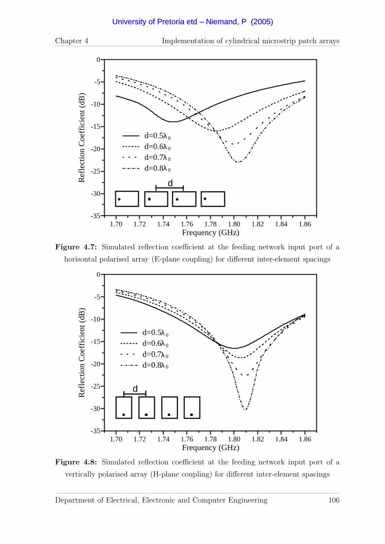
Chapter 4 Implementation of cylindrical microstrip patch arrays
-35
-30
-25
-20
-15
-10
-5
0
Ref
l ect
ion
Coe
ffic
ien t
(dB
)
1.70 1.72 1.74 1.76 1.78 1.80 1.82 1.84 1.86Frequency (GHz)
d=0.5d=0.6d=0.7d=0.8
d
λλλλ 0
0
0
0
Figure 4.7: Simulated reflection coefficient at the feeding network input port of a
horisontal polarised array (E-plane coupling) for different inter-element spacings
-35
-30
-25
-20
-15
-10
-5
0
Ref
l ect
ion
Coe
ffic
ien t
(dB
)
1.70 1.72 1.74 1.76 1.78 1.80 1.82 1.84 1.86Frequency (GHz)
d=0.5d=0.6d=0.7d=0.8
d
λ 0
λλ
0
0
λ 0
Figure 4.8: Simulated reflection coefficient at the feeding network input port of a
vertically polarised array (H-plane coupling) for different inter-element spacings
Department of Electrical, Electronic and Computer Engineering 106
UUnniivveerrssiittyy ooff PPrreettoorriiaa eettdd –– NNiieemmaanndd,, PP ((22000055))
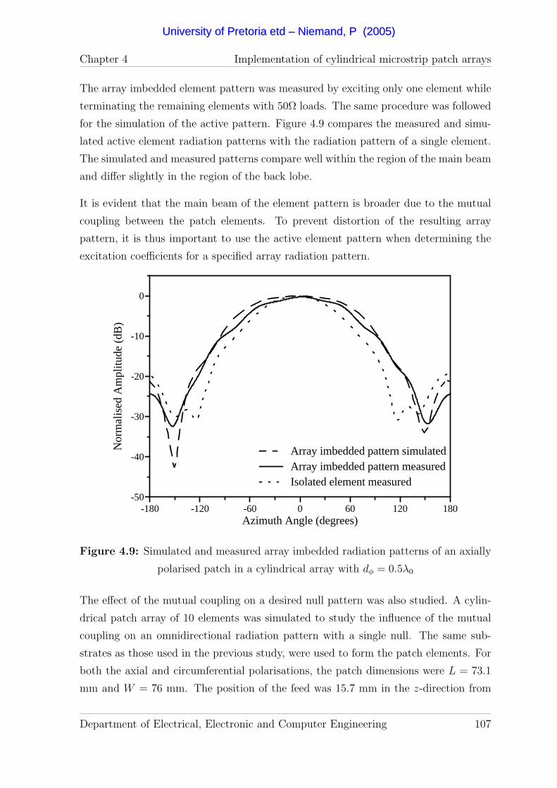
Chapter 4 Implementation of cylindrical microstrip patch arrays
The array imbedded element pattern was measured by exciting only one element while
terminating the remaining elements with 50Ω loads. The same procedure was followed
for the simulation of the active pattern. Figure 4.9 compares the measured and simu-
lated active element radiation patterns with the radiation pattern of a single element.
The simulated and measured patterns compare well within the region of the main beam
and differ slightly in the region of the back lobe.
It is evident that the main beam of the element pattern is broader due to the mutual
coupling between the patch elements. To prevent distortion of the resulting array
pattern, it is thus important to use the active element pattern when determining the
excitation coefficients for a specified array radiation pattern.
-50
-40
-30
-20
-10
0
Nor
mal
ised
Am
plitu
de (
dB)
-180 -120 -60 0 60 120 180Azimuth Angle (degrees)
Array imbedded pattern simulatedArray imbedded pattern measuredIsolated element measured
Figure 4.9: Simulated and measured array imbedded radiation patterns of an axially
polarised patch in a cylindrical array with dφ = 0.5λ0
The effect of the mutual coupling on a desired null pattern was also studied. A cylin-
drical patch array of 10 elements was simulated to study the influence of the mutual
coupling on an omnidirectional radiation pattern with a single null. The same sub-
strates as those used in the previous study, were used to form the patch elements. For
both the axial and circumferential polarisations, the patch dimensions were L = 73.1
mm and W = 76 mm. The position of the feed was 15.7 mm in the z-direction from
Department of Electrical, Electronic and Computer Engineering 107
UUnniivveerrssiittyy ooff PPrreettoorriiaa eettdd –– NNiieemmaanndd,, PP ((22000055))
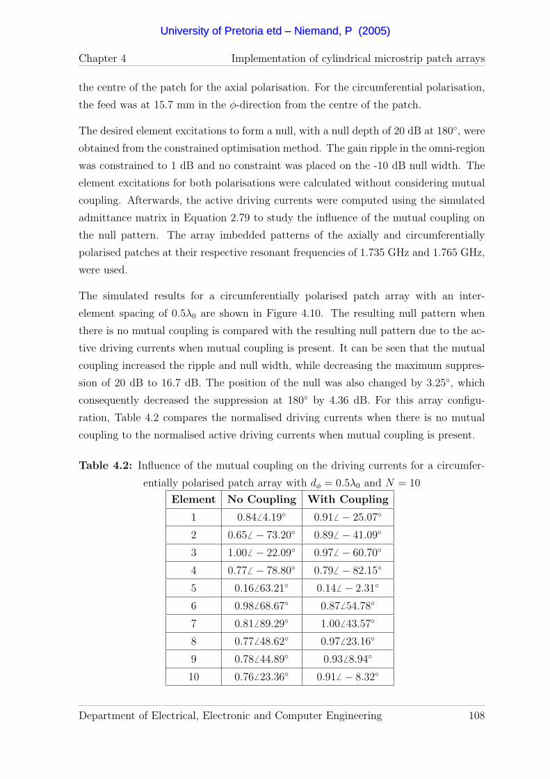
Chapter 4 Implementation of cylindrical microstrip patch arrays
the centre of the patch for the axial polarisation. For the circumferential polarisation,
the feed was at 15.7 mm in the φ-direction from the centre of the patch.
The desired element excitations to form a null, with a null depth of 20 dB at 180, were
obtained from the constrained optimisation method. The gain ripple in the omni-region
was constrained to 1 dB and no constraint was placed on the -10 dB null width. The
element excitations for both polarisations were calculated without considering mutual
coupling. Afterwards, the active driving currents were computed using the simulated
admittance matrix in Equation 2.79 to study the influence of the mutual coupling on
the null pattern. The array imbedded patterns of the axially and circumferentially
polarised patches at their respective resonant frequencies of 1.735 GHz and 1.765 GHz,
were used.
The simulated results for a circumferentially polarised patch array with an inter-
element spacing of 0.5λ0 are shown in Figure 4.10. The resulting null pattern when
there is no mutual coupling is compared with the resulting null pattern due to the ac-
tive driving currents when mutual coupling is present. It can be seen that the mutual
coupling increased the ripple and null width, while decreasing the maximum suppres-
sion of 20 dB to 16.7 dB. The position of the null was also changed by 3.25, which
consequently decreased the suppression at 180 by 4.36 dB. For this array configu-
ration, Table 4.2 compares the normalised driving currents when there is no mutual
coupling to the normalised active driving currents when mutual coupling is present.
Table 4.2: Influence of the mutual coupling on the driving currents for a circumfer-
entially polarised patch array with dφ = 0.5λ0 and N = 10
Element No Coupling With Coupling
1 0.846 4.19 0.916 − 25.07
2 0.656 − 73.20 0.896 − 41.09
3 1.006 − 22.09 0.976 − 60.70
4 0.776 − 78.80 0.796 − 82.15
5 0.16 6 63.21 0.14 6 − 2.31
6 0.98 6 68.67 0.87 6 54.78
7 0.81 6 89.29 1.00 6 43.57
8 0.77 6 48.62 0.97 6 23.16
9 0.78 6 44.89 0.936 8.94
10 0.76 6 23.36 0.91 6 − 8.32
Department of Electrical, Electronic and Computer Engineering 108
UUnniivveerrssiittyy ooff PPrreettoorriiaa eettdd –– NNiieemmaanndd,, PP ((22000055))

Chapter 4 Implementation of cylindrical microstrip patch arrays
Figure 4.11 shows the simulated patterns for a circumferentially polarised patch array
with an inter-element spacing of 0.65λ0. For this larger inter-element spacing, the mu-
tual coupling was smaller and the most significant observed change was in the ripple
in the omni-region of the null pattern. For this case, the ripple increased from 1 dB
to 2.86 dB, when the active element excitations are used. The results for the different
inter-element spacings are summarised in Table 4.3 and Table 4.4. The coupling co-
efficients in these tables are the mutual coupling between an element and its nearest
neighbour.
For the axially polarised patch array with an inter-element spacing of 0.5λ0, the results
are shown in Figure 4.12. The resulting null pattern when there is no mutual coupling
is compared with the resulting null pattern due to the active driving currents when
mutual coupling is present. Both the ripple and null width were increased by the
mutual coupling, while the maximum suppression was decreased by 1.46 dB. Table 4.5
compares the normalised driving currents when there is no mutual coupling to the
normalised active driving currents when mutual coupling is present.
Figure 4.13 shows the resulting patterns for this array with an inter-element spacing
of 0.65λ0. Although the mutual coupling is less for this larger inter-element spacing,
the distortion of null pattern is more significant. In this case, the ripple and maximum
suppression changed by 2.55 dB and 4.06 dB, respectively. Table 4.6 and Table 4.7
summarises the results for the different inter-element spacings.
The desired radiation pattern could not be obtained for inter-element spacings larger
than 0.7λ0 and 0.65λ0 for the circumferentially and axially polarised arrays, respec-
tively. This is due to the high ripple in the omnidirectional radiation pattern when
large inter-element spacings are utilised.
Greater changes in the null positions and null widths are observed for the circumferen-
tially polarised patch array. The change in the suppression at 180 and the change in
the maximum suppression decreases as the spacing increases and the mutual coupling
decreases for dφ ≤ 0.65λ0. For the larger inter-element spacing, as seen for dφ = 0.7λ0,
the element excitations tend to be more sensitive to the mutual coupling, although
it is less than -20 dB. For the axial polarisation, the change in the suppression at
180 increases although the coupling decreases. For this polarisation, the increasing
inter-element spacing thus makes the element excitations more sensitive to the mutual
coupling.
Department of Electrical, Electronic and Computer Engineering 109
UUnniivveerrssiittyy ooff PPrreettoorriiaa eettdd –– NNiieemmaanndd,, PP ((22000055))

Chapter 4 Implementation of cylindrical microstrip patch arrays
-20
-15
-10
-5
0N
orm
alis
ed A
mpl
itude
(dB
)
0 60 120 180 240 300 360Azimuth Angle (degrees)
Without couplingWith coupling
Figure 4.10: Normalised amplitude patterns of a circumferentially polarised patch
array with dφ = 0.5λ0 and N = 10
-25
-20
-15
-10
-5
0
Nor
mal
ised
Am
plitu
de (
dB)
0 60 120 180 240 300 360Azimuth Angle (degrees)
Without couplingWith coupling
Figure 4.11: Normalised amplitude patterns of a circumferentially polarised patch
array with dφ = 0.65λ0 and N = 10
Department of Electrical, Electronic and Computer Engineering 110
UUnniivveerrssiittyy ooff PPrreettoorriiaa eettdd –– NNiieemmaanndd,, PP ((22000055))

Chapter 4 Implementation of cylindrical microstrip patch arrays
Table 4.3: Influence of the mutual coupling on the desired null pattern for a circum-
ferentially polarised patch array
Spacing Coupling Change in Change in
(λ0) (dB) suppression maximum
at 180 (dB) suppression
(dB)
0.5 -10.7 4.36 3.3
0.55 -13.3 4.23 1.95
0.6 -16.1 1.37 0.05
0.65 -18.8 1.21 -0.01
0.7 -21.1 4.3 3.52
Table 4.4: Influence of the mutual coupling on the desired null pattern for a circum-
ferentially polarised patch array (continued)
Spacing Change in Change in Change in
(λ0) ripple null position null width
(dB) (deg) (deg)
0.5 0.14 3.25 7.80
0.55 0.40 4 7.69
0.6 1.51 2.25 6.69
0.65 1.86 2.25 4.34
0.7 4.63 2 -3.45
The inter-element spacing thus plays an important role in the choice of an array con-
figuration. For small inter-element spacings in a circumferentially polarised array, the
larger coupling between the elements has a greater influence on the radiation pattern.
On the other hand, the use of large inter-element spacings makes the desired element
excitations more sensitive to the mutual coupling for both polarisations. The coupling
between axially polarised patches is smaller and the radiation pattern is less effected
for small inter-element spacing.
Department of Electrical, Electronic and Computer Engineering 111
UUnniivveerrssiittyy ooff PPrreettoorriiaa eettdd –– NNiieemmaanndd,, PP ((22000055))
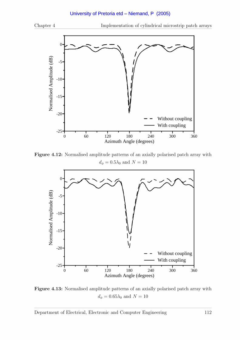
Chapter 4 Implementation of cylindrical microstrip patch arrays
-25
-20
-15
-10
-5
0
Nor
mal
ised
Am
plitu
de (
dB)
0 60 120 180 240 300 360Azimuth Angle (degrees)
Without couplingWith coupling
Figure 4.12: Normalised amplitude patterns of an axially polarised patch array with
dφ = 0.5λ0 and N = 10
-25
-20
-15
-10
-5
0
Nor
mal
ised
Am
plitu
de (
dB)
0 60 120 180 240 300 360Azimuth Angle (degrees)
Without couplingWith coupling
Figure 4.13: Normalised amplitude patterns of an axially polarised patch array with
dφ = 0.65λ0 and N = 10
Department of Electrical, Electronic and Computer Engineering 112
UUnniivveerrssiittyy ooff PPrreettoorriiaa eettdd –– NNiieemmaanndd,, PP ((22000055))

Chapter 4 Implementation of cylindrical microstrip patch arrays
Table 4.5: Influence of the mutual coupling on the driving currents for a axially
polarised patch array with dφ = 0.5λ0 and N = 10
Element No Coupling With Coupling
1 0.79 6 12.14 0.81 6 − 5.27
2 0.706 − 6.55 0.846 − 22.51
3 0.956 − 16.17 0.846 − 35.48
4 0.756 − 71.78 0.796 − 73.28
5 0.18 6 62.69 0.13 6 58.73
6 1.00 6 78.36 1.00 6 72.14
7 0.73 6 91.40 0.76 6 60.52
8 0.81 6 59.14 0.92 6 47.32
9 0.76 6 45.93 0.77 6 28.57
10 0.77 6 28.71 0.88 6 12.09
Table 4.6: Influence of the mutual coupling on the desired null pattern for a axially
polarised patch array
Spacing Coupling Change in Change in
(λ0) (dB) suppression maximum
at 180 (dB) suppression
(dB)
0.5 -17.6 2.08 1.46
0.55 -20.1 2.67 2.08
0.6 -22.5 2.67 1.83
0.65 -24.3 4.31 4.06
From Table 4.3 and Table 4.4, it is observed that for small inter-element spacing in the
circumferential polarisation, the mutual coupling must be compensated for in order to
obtain the desired radiation pattern. The compensation is also needed to correct the
degree of suppression in a specified direction for all inter-element spacings and both
polarisations.
Department of Electrical, Electronic and Computer Engineering 113
UUnniivveerrssiittyy ooff PPrreettoorriiaa eettdd –– NNiieemmaanndd,, PP ((22000055))

Chapter 4 Implementation of cylindrical microstrip patch arrays
Table 4.7: Influence of the mutual coupling on the desired null pattern for a axially
polarised patch array (continued)
Spacing Change in Change in Change in
(λ0) ripple null position null width
(dB) (deg) (deg)
0.5 1.14 1.25 3.28
0.55 1.47 1 1.22
0.6 1.47 1.75 0.08
0.65 2.55 1.75 -0.23
4.3 Mutual coupling compensation
4.3.1 Mutual coupling compensation for linear patch arrays
Paragraph 2.4.3 discusses a technique in which the geometries of the elements are varied
to provide matched and equal driving impedances for all the antenna elements, given a
required set of element excitations. From Equation 2.80, the driving impedances may
be written as:
Zam = Zs
mm(Lm, ym) +N∑
n=1n 6=m
Zmn(Ln, Lm, yn, ym)In
Im
, (4.1)
where Lm and ym are the length and feed position of the m-th patch antenna ele-
ment, respectively. The length and feed position of the n-th neighbouring antenna
element are represented by Ln and yn, respectively. Both the self impedance and mu-
tual impedances are expressed as functions of the length and feed positions. Although
the above impedances also vary with the widths and heights of the patch antennae,
these dimensions are kept constant to reduce the dimensionality of variable space.
A commercial electromagnetic software package [100] which utilises the method of
moments, is used to obtain Zsmm and Zmn for different lengths and feed positions.
For the linear array configuration in Figure 4.6, Zmn has a low sensitivity to small
variations in the feed positions and the dimensionality of Zmn can thus be even further
reduced. The self and mutual impedances are computed for linearly spaced values
Department of Electrical, Electronic and Computer Engineering 114
UUnniivveerrssiittyy ooff PPrreettoorriiaa eettdd –– NNiieemmaanndd,, PP ((22000055))

Chapter 4 Implementation of cylindrical microstrip patch arrays
of the lengths and feed positions and are placed in two lookup tables. One lookup
table is populated with the self impedance values with respect to the lengths and
feed-positions of a single antenna element. Another lookup table is populated with
the mutual impedance values with respect to the lengths of two neighbouring antenna
elements. A least squares optimisation algorithm is used to determine the lengths and
feed positions at which the driving impedances of all the patches are equal to 50Ω. N
lengths and N feed positions are used as the variables and the algorithm interpolates
between the computed impedance values using a bicubic spline algorithm. For each
antenna element an error in the real part of impedance as well as an error in the
imaginary part of the impedance is calculated. The cost function is then determined as
the sum of the 2N squared errors. The least squares optimisation algorithm determines
the N lengths and N feed positions which minimise this cost function.
An example in which the mutual compensation technique is applied to a linear patch
array, is incorporated into the test case in paragraph 4.4.1.
4.3.2 Mutual coupling compensation for cylindrical arrays
The mutual coupling compensation technique described in paragraph 4.3.1 for the
linear patch array will also be used for the cylindrical patch arrays. For the cylindrical
arrays, Lm and ym in equation 4.1 are respectively the length and feed position of the
m-th patch element along the direction of its polarisation.
The look-up table, which is used to search for the necessary lengths and feed positions
to adjust the active driving impedances to 50Ω, is populated using simulation results
from the FDTD software.
As an example, the lengths and feed positions were found to correct the null pattern
in Figure 4.10 for the axially polarised array with dφ = 0.5λ0 and N = 10. The
starting values used by the optimisation algorithm for all n elements, were Ln=73.1
mm and yn=20.85 mm. A graphical representation of the variable space for the self-
impedance is shown on a Smith chart in Figure 4.14. The variable space is shown
for 71.6mm ≤ Ln ≤ 74.6mm and 4.85mm ≤ yn ≤ 26.85mm. During the search for
the appropriate lengths and feed positions, it was assumed that small changes in the
lengths and feed positions, do not have a significant effect on the mutual coupling and
was considered to stay constant. The resulting lengths and feed positions needed to
Department of Electrical, Electronic and Computer Engineering 115
UUnniivveerrssiittyy ooff PPrreettoorriiaa eettdd –– NNiieemmaanndd,, PP ((22000055))
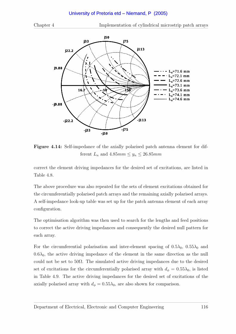
Chapter 4 Implementation of cylindrical microstrip patch arrays
50
j50
-j50
j22.2
j9 .88
-j9 .88
-j22.2
16.7 150
j75
j113
-j113
-j75
j33
-j33
Ln=72.1 mmLn=72.6 mmLn=73.1 mmLn=73.6 mmLn=74.1 mmLn=74.6 mm
Ln=71.6 mm
50
j50
-j50
j22.2
j9 .88
-j9 .88
-j22.2
16.7 150
j75
j113
-j113
-j75
j33
-j33
Ln=72.1 mmLn=72.6 mmLn=73.1 mmLn=73.6 mmLn=74.1 mmLn=74.6 mm
Ln=71.6 mm
50
j50
-j50
j22.2
j9 .88
-j9 .88
-j22.2
16.7 150
j75
j113
-j113
-j75
j33
-j33
Ln=72.1 mmLn=72.6 mmLn=73.1 mmLn=73.6 mmLn=74.1 mmLn=74.6 mm
Ln=71.6 mm
Figure 4.14: Self-impedance of the axially polarised patch antenna element for dif-
ferent Ln and 4.85mm ≤ yn ≤ 26.85mm
correct the element driving impedances for the desired set of excitations, are listed in
Table 4.8.
The above procedure was also repeated for the sets of element excitations obtained for
the circumferentially polarised patch arrays and the remaining axially polarised arrays.
A self-impedance look-up table was set up for the patch antenna element of each array
configuration.
The optimisation algorithm was then used to search for the lengths and feed positions
to correct the active driving impedances and consequently the desired null pattern for
each array.
For the circumferential polarisation and inter-element spacing of 0.5λ0, 0.55λ0 and
0.6λ0, the active driving impedance of the element in the same direction as the null
could not be set to 50Ω. The simulated active driving impedances due to the desired
set of excitations for the circumferentially polarised array with dφ = 0.55λ0, is listed
in Table 4.9. The active driving impedances for the desired set of excitations of the
axially polarised array with dφ = 0.55λ0, are also shown for comparison.
Department of Electrical, Electronic and Computer Engineering 116
UUnniivveerrssiittyy ooff PPrreettoorriiaa eettdd –– NNiieemmaanndd,, PP ((22000055))
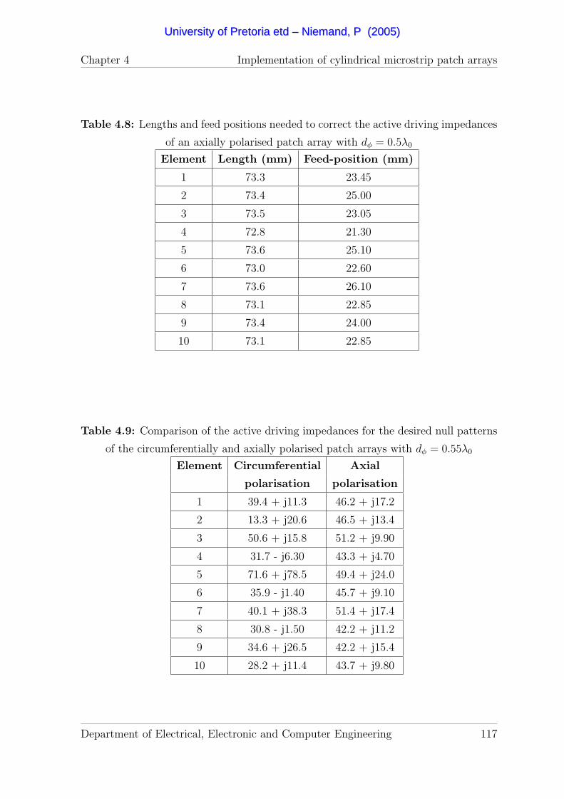
Chapter 4 Implementation of cylindrical microstrip patch arrays
Table 4.8: Lengths and feed positions needed to correct the active driving impedances
of an axially polarised patch array with dφ = 0.5λ0
Element Length (mm) Feed-position (mm)
1 73.3 23.45
2 73.4 25.00
3 73.5 23.05
4 72.8 21.30
5 73.6 25.10
6 73.0 22.60
7 73.6 26.10
8 73.1 22.85
9 73.4 24.00
10 73.1 22.85
Table 4.9: Comparison of the active driving impedances for the desired null patterns
of the circumferentially and axially polarised patch arrays with dφ = 0.55λ0
Element Circumferential Axial
polarisation polarisation
1 39.4 + j11.3 46.2 + j17.2
2 13.3 + j20.6 46.5 + j13.4
3 50.6 + j15.8 51.2 + j9.90
4 31.7 - j6.30 43.3 + j4.70
5 71.6 + j78.5 49.4 + j24.0
6 35.9 - j1.40 45.7 + j9.10
7 40.1 + j38.3 51.4 + j17.4
8 30.8 - j1.50 42.2 + j11.2
9 34.6 + j26.5 42.2 + j15.4
10 28.2 + j11.4 43.7 + j9.80
Department of Electrical, Electronic and Computer Engineering 117
UUnniivveerrssiittyy ooff PPrreettoorriiaa eettdd –– NNiieemmaanndd,, PP ((22000055))
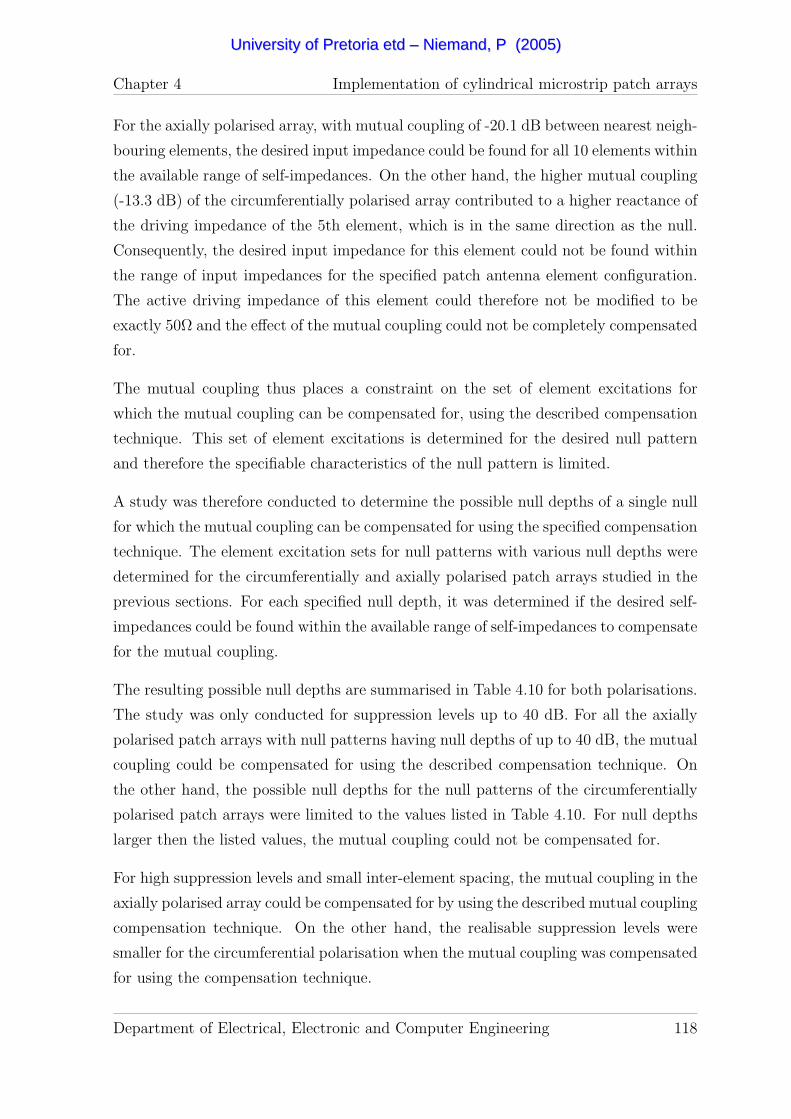
Chapter 4 Implementation of cylindrical microstrip patch arrays
For the axially polarised array, with mutual coupling of -20.1 dB between nearest neigh-
bouring elements, the desired input impedance could be found for all 10 elements within
the available range of self-impedances. On the other hand, the higher mutual coupling
(-13.3 dB) of the circumferentially polarised array contributed to a higher reactance of
the driving impedance of the 5th element, which is in the same direction as the null.
Consequently, the desired input impedance for this element could not be found within
the range of input impedances for the specified patch antenna element configuration.
The active driving impedance of this element could therefore not be modified to be
exactly 50Ω and the effect of the mutual coupling could not be completely compensated
for.
The mutual coupling thus places a constraint on the set of element excitations for
which the mutual coupling can be compensated for, using the described compensation
technique. This set of element excitations is determined for the desired null pattern
and therefore the specifiable characteristics of the null pattern is limited.
A study was therefore conducted to determine the possible null depths of a single null
for which the mutual coupling can be compensated for using the specified compensation
technique. The element excitation sets for null patterns with various null depths were
determined for the circumferentially and axially polarised patch arrays studied in the
previous sections. For each specified null depth, it was determined if the desired self-
impedances could be found within the available range of self-impedances to compensate
for the mutual coupling.
The resulting possible null depths are summarised in Table 4.10 for both polarisations.
The study was only conducted for suppression levels up to 40 dB. For all the axially
polarised patch arrays with null patterns having null depths of up to 40 dB, the mutual
coupling could be compensated for using the described compensation technique. On
the other hand, the possible null depths for the null patterns of the circumferentially
polarised patch arrays were limited to the values listed in Table 4.10. For null depths
larger then the listed values, the mutual coupling could not be compensated for.
For high suppression levels and small inter-element spacing, the mutual coupling in the
axially polarised array could be compensated for by using the described mutual coupling
compensation technique. On the other hand, the realisable suppression levels were
smaller for the circumferential polarisation when the mutual coupling was compensated
for using the compensation technique.
Department of Electrical, Electronic and Computer Engineering 118
UUnniivveerrssiittyy ooff PPrreettoorriiaa eettdd –– NNiieemmaanndd,, PP ((22000055))

Chapter 4 Implementation of cylindrical microstrip patch arrays
Table 4.10: Comparison of possible null depths for circumferentially and axially po-
larised patch arrays with N=10
Spacing (dφ) Circumferential Axial
(λ0) polarisation polarisation
0.5 -10 dB -40 dB
0.55 -15 dB -40 dB
0.6 -15 dB -40 dB
0.65 -25 dB -40 dB
4.4 Test cases
4.4.1 Linear patch array test case
A four element microstrip patch array with E-plane coupling was chosen to confirm
experimentally the proposed coupling compensation technique. Initially, Ln, Wn and
yn in Figure 4.6 were 62.8mm, 65mm and 12.9mm for all n, respectively. The inter-
element spacing was d = 0.65λ0 and the self and mutual impedances of the array were
computed for different lengths and feed positions using Ln=62.8mm and yn=12.9mm
as the centre variable values of the look-up tables.
A graphical presentation of the variable space for the self impedance is shown on a
Smith chart in Figure 4.15. Each impedance curve is formed by keeping Ln constant
and varying yn between 8.9mm and 15.9mm. The optimisation algorithm is constrained
to search only within this available self impedance space.
Careful attention should be paid to the element radiation pattern when setting up the
look-up tables and variable space. Significant changes in the radiation pattern of the
element should be avoided to prevent distortion of the total array radiation pattern.
When the probe feed is put too close to the edge of the patch, the probe radiation may
alter the element radiation pattern. If the length of the patch is varied too much, the
beamwidth of the main beam in the element radiation pattern will be modified. The
extent of these effects will vary between patch antenna element configurations.
The optimisation algorithm uses Ln=62.8mm and yn=12.9mm as the starting values for
all n elements to search for the lengths and feed positions where the driving impedances
of all the patches are 50Ω. The resulting lengths are: L1=L4=63.2mm, y1=y4=11mm,
Department of Electrical, Electronic and Computer Engineering 119
UUnniivveerrssiittyy ooff PPrreettoorriiaa eettdd –– NNiieemmaanndd,, PP ((22000055))
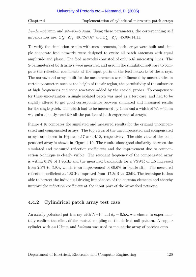
Chapter 4 Implementation of cylindrical microstrip patch arrays
L2=L3=63.7mm and y2=y3=8.9mm. Using these parameters, the corresponding self
impendances are: Zs11=Zs
44=48.72-j7.87 and Zs22=Zs
33=45.08-j14.11.
To verify the simulation results with measurements, both arrays were built and sim-
ple cooperate feed networks were designed to excite all patch antennas with equal
amplitude and phase. The feed networks consisted of only 50Ω microstrip lines. The
S-parameters of both arrays were measured and used in the simulation software to com-
pute the reflection coefficients at the input ports of the feed networks of the arrays.
The narrowband arrays built for the measurements were influenced by uncertainties in
certain parameters such as the height of the air region, the permittivity of the substrate
at high frequencies and some reactance added by the coaxial probes. To compensate
for these uncertainties, a single isolated patch was used as a test case, and had to be
slightly altered to get good correspondence between simulated and measured results
for the single patch. The width had to be increased by 4mm and a width of Wn=69mm
was subsequently used for all the patches of both experimental arrays.
Figure 4.16 compares the simulated and measured results for the original uncompen-
sated and compensated arrays. The top views of the uncompensated and compensated
arrays are shown in Figures 4.17 and 4.18, respectively. The side view of the com-
pensated array is shown in Figure 4.19. The results show good similarity between the
simulated and measured reflection coefficients and the improvement due to compen-
sation technique is clearly visible. The resonant frequency of the compensated array
is within 0.1% of 1.8GHz and the measured bandwidth for a VSWR of 1.5 increased
from 2.3% to 3.9%, which is an improvement of 69.6% in bandwidth. The measured
reflection coefficient at 1.8GHz improved from -17.3dB to -32dB. The technique is thus
able to correct the individual driving impedances of the antenna elements and thereby
improve the reflection coefficient at the input port of the array feed network.
4.4.2 Cylindrical patch array test case
An axially polarised patch array with N=10 and dφ = 0.5λ0 was chosen to experimen-
tally confirm the effect of the mutual coupling on the desired null pattern. A copper
cylinder with a=127mm and h=2mm was used to mount the array of patches onto.
Department of Electrical, Electronic and Computer Engineering 120
UUnniivveerrssiittyy ooff PPrreettoorriiaa eettdd –– NNiieemmaanndd,, PP ((22000055))
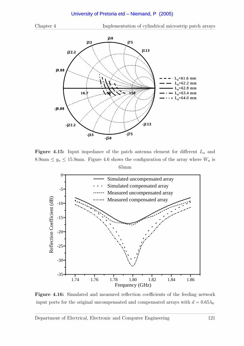
Chapter 4 Implementation of cylindrical microstrip patch arrays
50
j50
-j50
j22.2
j9 .88
-j22.2
16.7 150
j75
j113
-j113
-j75
j33
-j33
-j9 .88
Ln=61.6 mmLn=62.2 mmLn=62.8 mmLn=63.4 mmLn=64.0 mm
50
j50
-j50
j22.2
j9 .88
-j22.2
16.7 150
j75
j113
-j113
-j75
j33
-j33
-j9 .88
Ln=61.6 mmLn=62.2 mmLn=62.8 mmLn=63.4 mmLn=64.0 mm
Figure 4.15: Input impedance of the patch antenna element for different Ln and
8.9mm ≤ yn ≤ 15.9mm. Figure 4.6 shows the configuration of the array where Wn is
65mm
-35
-30
-25
-20
-15
-10
-5
0
Ref
l ect
ion
Coe
ffic
ien t
(dB
)
1.74 1.76 1.78 1.80 1.82 1.84 1.86Frequency (GHz)
Simulated uncompensated arraySimulated compensated arrayMeasured uncompensated arrayMeasured compensated array
Figure 4.16: Simulated and measured reflection coefficients of the feeding network
input ports for the original uncompensated and compensated arrays with d = 0.65λ0
Department of Electrical, Electronic and Computer Engineering 121
UUnniivveerrssiittyy ooff PPrreettoorriiaa eettdd –– NNiieemmaanndd,, PP ((22000055))

Chapter 4 Implementation of cylindrical microstrip patch arrays
Figure 4.17: Top view of the original uncompensated linear microstrip patch antenna
array
Figure 4.18: Top view of the compensated linear microstrip patch antenna array
Department of Electrical, Electronic and Computer Engineering 122
UUnniivveerrssiittyy ooff PPrreettoorriiaa eettdd –– NNiieemmaanndd,, PP ((22000055))

Chapter 4 Implementation of cylindrical microstrip patch arrays
Figure 4.19: Side view of the compensated linear microstrip patch antenna array
The cylindrical patch antenna element was designed for a measured resonant frequency
of 1.8 GHz, using the measured reflection coefficient data in paragraph 4.1 for the
refinement of the design. The resulting dimensions were L=73.6 mm and W=76 mm,
with the feed position at 16.6 mm from the centre of the patch in the z-direction. The
resonant frequency and reflection coefficient, obtained from the simulation of the patch
element with the FDTD software, were 1.727 GHz and -32.8 dB, respectively.
The cylindrical array was manufactured by etching the patch element array onto the
thin layer of FR4 and wrapping it around the cylinder. The 5mm air gap was estab-
lished by using 5mm polystyrene strips which were also wrapped around the cylinder.
To excite the patch elements individually, each element was provided with a probe feed
and a coaxial connector.
When the radiation pattern measurements were performed for the first set-up, signifi-
cant differences were found between the active element patterns. This was due to the
slight oval shape of the cylinder. Two PVC discs were then inserted at the bottom
and top of the cylinder to ensure that the cylinder maintains a circular shape. The
bottom PVC disc also provided the capability for mounting the cylinder on a post and
for rotating it around its centre. Figures 4.20 and 4.21 provide the side and top view
of the manufactured array, respectively.
The radiation pattern measurement was done in a compact measurement range. The
active element pattern was measured for each element by exciting the particular element
and terminating the feeds of the rest of the elements with 50Ω loads. The S-matrix
of the array was measured using a network analyser in a measurement room partially
filled with absorbing material. All measurements were done at 1.8 GHz.
Department of Electrical, Electronic and Computer Engineering 123
UUnniivveerrssiittyy ooff PPrreettoorriiaa eettdd –– NNiieemmaanndd,, PP ((22000055))
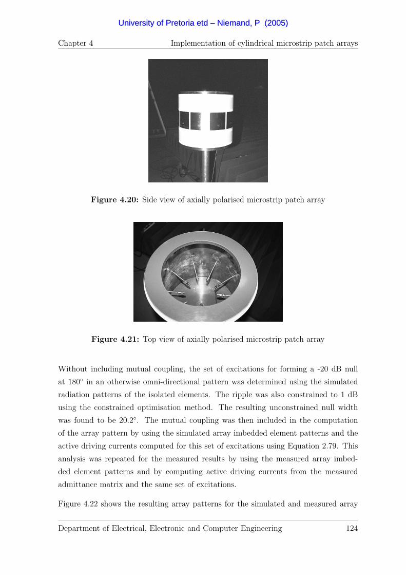
Chapter 4 Implementation of cylindrical microstrip patch arrays
Figure 4.20: Side view of axially polarised microstrip patch array
Figure 4.21: Top view of axially polarised microstrip patch array
Without including mutual coupling, the set of excitations for forming a -20 dB null
at 180 in an otherwise omni-directional pattern was determined using the simulated
radiation patterns of the isolated elements. The ripple was also constrained to 1 dB
using the constrained optimisation method. The resulting unconstrained null width
was found to be 20.2. The mutual coupling was then included in the computation
of the array pattern by using the simulated array imbedded element patterns and the
active driving currents computed for this set of excitations using Equation 2.79. This
analysis was repeated for the measured results by using the measured array imbed-
ded element patterns and by computing active driving currents from the measured
admittance matrix and the same set of excitations.
Figure 4.22 shows the resulting array patterns for the simulated and measured array
Department of Electrical, Electronic and Computer Engineering 124
UUnniivveerrssiittyy ooff PPrreettoorriiaa eettdd –– NNiieemmaanndd,, PP ((22000055))

Chapter 4 Implementation of cylindrical microstrip patch arrays
characteristics. The most significant changes in the array radiation pattern when the
mutual coupling is included in the analyses, are the decrease in the null depth and the
increase in the null width. For the simulated characteristics, the null depth decreased
by 5.2 dB, while the null width increased by 3.7. The null depth decreased by 3.4
dB and the null width increased by 2.9 for the measured array characteristics. The
differences between the measured and simulated results are partially caused by the
manufacturing tolerances. The input impedances of the antenna elements are sensitive
to small variations in the height of the air layer underneath the patch. Any skewness
in the probe feed of the patch antenna will also cause the input impedance and the
array imbedded element pattern to differ from the simulated results. The differences
between the measured and simulated results discussed in paragraph 4.1, also contribute
the discrepancies between the simulated and measured results.
For this axially polarised cylindrical array, the length and feed positions of the antenna
elements to compensate for the mutual coupling, were found. The look-up table of
self-impedances was populated using simulation results. The mutual impedances was
assumed to vary little for small changes in the patch lengths and feed positions and was
kept constant in the optimisation algorithm. The resulting lengths and feed positions
are listed in Table 4.11.
To study the resulting array pattern after the mutual coupling compensation, the
cylindrical array was simulated with the modified patch elements. The simulations
were done over the bandwidth (for VSWR ≤ 2) of the isolated patch element at 1.696,
1.727 and 1.760 GHz. Figure 4.23 compares the the resulting null pattern before
and after the modification of the dimensions of the antenna elements. The resulting
ripple was 1.31 dB, while the null depth and null width were -19.5 dB and 20.6,
respectively. To be practical, the lengths and feed positions of the patch elements were
only incremented or decremented in steps of 0.1mm. The driving impedances of the
patch elements were thus not adjusted to be exactly 50Ω. Small changes in the mutual
coupling between the modified antenna elements also contributed to the higher than
expected ripple. The null width and null depth compared well to the null width (20.2)
and null depth (-20 dB) when mutual coupling was not included in the analysis.
Department of Electrical, Electronic and Computer Engineering 125
UUnniivveerrssiittyy ooff PPrreettoorriiaa eettdd –– NNiieemmaanndd,, PP ((22000055))
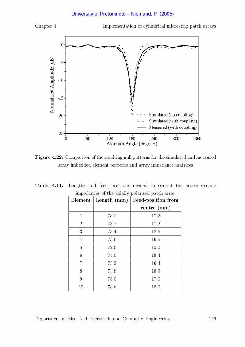
Chapter 4 Implementation of cylindrical microstrip patch arrays
-25
-20
-15
-10
-5
0
Nor
mal
ised
Am
plitu
de (
dB)
0 60 120 180 240 300 360Azimuth Angle (degrees)
Simulated (no coupling)Simulated (with coupling)Measured (with coupling)
Figure 4.22: Comparison of the resulting null patterns for the simulated and measured
array imbedded element patterns and array impedance matrices
Table 4.11: Lengths and feed positions needed to correct the active driving
impedances of the axially polarised patch array
Element Length (mm) Feed-position from
centre (mm)
1 73.2 17.2
2 73.2 17.2
3 73.4 18.6
4 73.6 16.6
5 72.6 15.0
6 74.0 19.4
7 73.2 16.4
8 73.8 18.9
9 73.0 17.0
10 73.6 18.0
Department of Electrical, Electronic and Computer Engineering 126
UUnniivveerrssiittyy ooff PPrreettoorriiaa eettdd –– NNiieemmaanndd,, PP ((22000055))
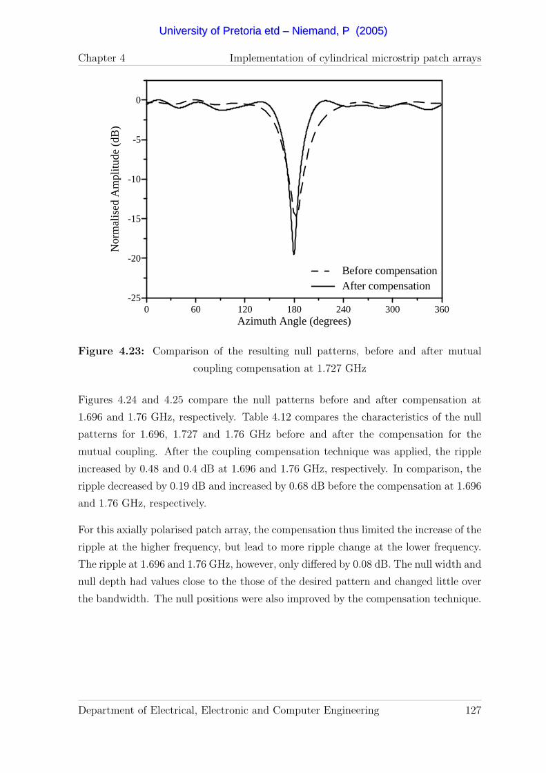
Chapter 4 Implementation of cylindrical microstrip patch arrays
-25
-20
-15
-10
-5
0
Nor
mal
ised
Am
plitu
de (
dB)
0 60 120 180 240 300 360Azimuth Angle (degrees)
Before compensationAfter compensation
Figure 4.23: Comparison of the resulting null patterns, before and after mutual
coupling compensation at 1.727 GHz
Figures 4.24 and 4.25 compare the null patterns before and after compensation at
1.696 and 1.76 GHz, respectively. Table 4.12 compares the characteristics of the null
patterns for 1.696, 1.727 and 1.76 GHz before and after the compensation for the
mutual coupling. After the coupling compensation technique was applied, the ripple
increased by 0.48 and 0.4 dB at 1.696 and 1.76 GHz, respectively. In comparison, the
ripple decreased by 0.19 dB and increased by 0.68 dB before the compensation at 1.696
and 1.76 GHz, respectively.
For this axially polarised patch array, the compensation thus limited the increase of the
ripple at the higher frequency, but lead to more ripple change at the lower frequency.
The ripple at 1.696 and 1.76 GHz, however, only differed by 0.08 dB. The null width and
null depth had values close to the those of the desired pattern and changed little over
the bandwidth. The null positions were also improved by the compensation technique.
Department of Electrical, Electronic and Computer Engineering 127
UUnniivveerrssiittyy ooff PPrreettoorriiaa eettdd –– NNiieemmaanndd,, PP ((22000055))
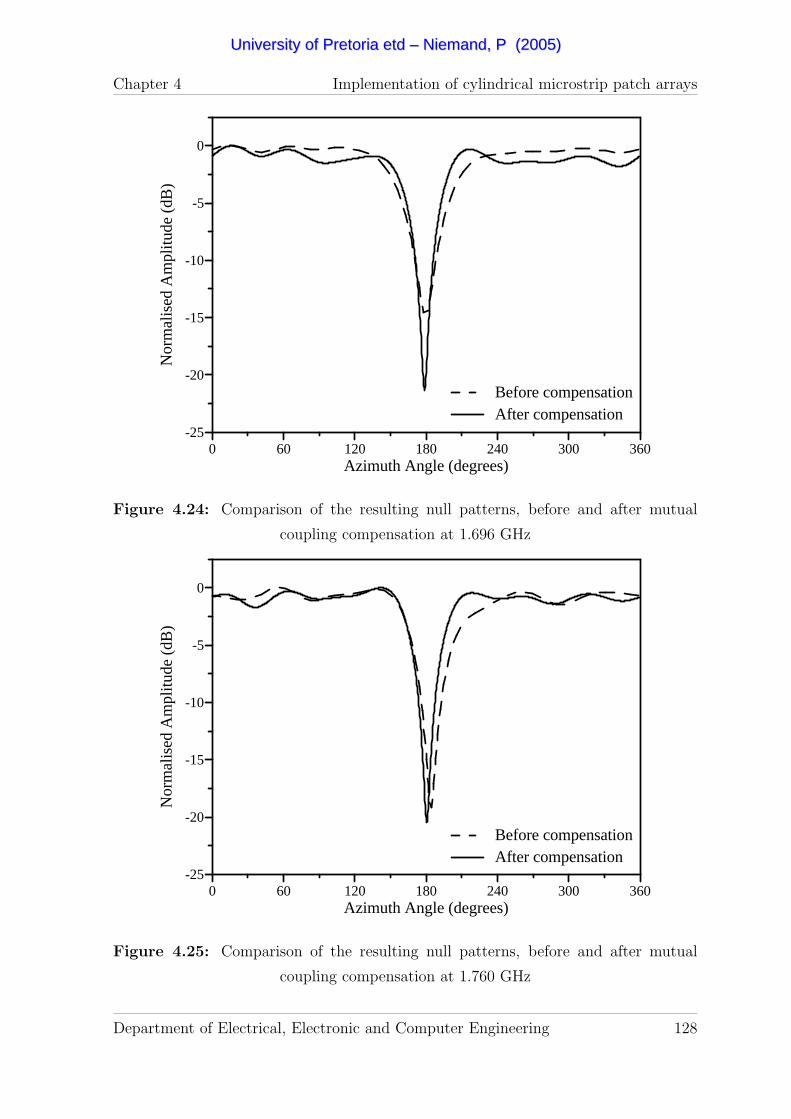
Chapter 4 Implementation of cylindrical microstrip patch arrays
-25
-20
-15
-10
-5
0
Nor
mal
ised
Am
plitu
de (
dB)
0 60 120 180 240 300 360Azimuth Angle (degrees)
Before compensationAfter compensation
Figure 4.24: Comparison of the resulting null patterns, before and after mutual
coupling compensation at 1.696 GHz
-25
-20
-15
-10
-5
0
Nor
mal
ised
Am
plitu
de (
dB)
0 60 120 180 240 300 360Azimuth Angle (degrees)
Before compensationAfter compensation
Figure 4.25: Comparison of the resulting null patterns, before and after mutual
coupling compensation at 1.760 GHz
Department of Electrical, Electronic and Computer Engineering 128
UUnniivveerrssiittyy ooff PPrreettoorriiaa eettdd –– NNiieemmaanndd,, PP ((22000055))
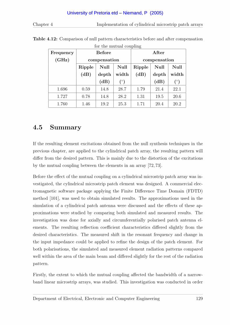
Chapter 4 Implementation of cylindrical microstrip patch arrays
Table 4.12: Comparison of null pattern characteristics before and after compensation
for the mutual coupling
Frequency Before After
(GHz) compensation compensation
Ripple Null Null Ripple Null Null
(dB) depth width (dB) depth width
(dB) () (dB) ()
1.696 0.59 14.8 28.7 1.79 21.4 22.1
1.727 0.78 14.8 28.2 1.31 19.5 20.6
1.760 1.46 19.2 25.3 1.71 20.4 20.2
4.5 Summary
If the resulting element excitations obtained from the null synthesis techniques in the
previous chapter, are applied to the cylindrical patch array, the resulting pattern will
differ from the desired pattern. This is mainly due to the distortion of the excitations
by the mutual coupling between the elements in an array [72,73].
Before the effect of the mutual coupling on a cylindrical microstrip patch array was in-
vestigated, the cylindrical microstrip patch element was designed. A commercial elec-
tromagnetic software package applying the Finite Difference Time Domain (FDTD)
method [101], was used to obtain simulated results. The approximations used in the
simulation of a cylindrical patch antenna were discussed and the effects of these ap-
proximations were studied by comparing both simulated and measured results. The
investigation was done for axially and circumferentially polarised patch antenna el-
ements. The resulting reflection coefficient characteristics differed slightly from the
desired characteristics. The measured shift in the resonant frequency and change in
the input impedance could be applied to refine the design of the patch element. For
both polarisations, the simulated and measured element radiation patterns compared
well within the area of the main beam and differed slightly for the rest of the radiation
pattern.
Firstly, the extent to which the mutual coupling affected the bandwidth of a narrow-
band linear microstrip arrays, was studied. This investigation was conducted in order
Department of Electrical, Electronic and Computer Engineering 129
UUnniivveerrssiittyy ooff PPrreettoorriiaa eettdd –– NNiieemmaanndd,, PP ((22000055))

Chapter 4 Implementation of cylindrical microstrip patch arrays
to study the improvement in the bandwidth due to the use of a mutual coupling com-
pensation technique. The study was conducted for a four element linear microstrip
patch array with a cooperate feed network and the results were compared for different
inter-element spacing and polarisations. It was seen that both the minimum of the
reflection coefficient at the input port of the feeding network and the resonant fre-
quency are influenced by the mutual coupling. For a horizontally polarised array with
E-plane coupling and an inter-element spacing of 0.5λ0, the resonant frequency was
shifted by 2.8%, which is close to the bandwidth of an isolated element. As expected,
the effect of the mutual coupling on the bandwidth and resonant frequency was less for
larger inter-element spacing. The resonant frequency and bandwidth was less affected
for a vertically polarised array with H-plane coupling due to the smaller magnitude
of this coupling. The reflection coefficient, however, was -16.5 dB for the smallest
inter-element spacing.
It was evident that the characteristics of narrowband arrays were affected by the mutual
coupling. A high coupling factor could alter the resonant frequency to such an extent
that the active bandwidth falls outside the desired bandwidth of the array. To match
the desired and active characteristics of the linear patch arrays, a mutual coupling
compensation technique was needed.
During null synthesis, erroneous excitations due to the mutual coupling lead to null
filling and null position errors [53, 74]. The nulls introduced in the beam patterns of
linear monopole arrays were found to be shifted or filled due to the mutual coupling [74].
Abele [53] studied the effect of the mutual coupling on the null pattern of a cylindrical
dipole array and concluded that the coupling needed to be compensated for to prevent
distortion of the null pattern characteristics. In this chapter, an investigation into the
extent to which the mutual coupling has an influence on the null pattern of a cylindrical
microstrip patch array was done.
The coupling in an array has an effect on the array imbedded radiation pattern of the
element. Heberling et al. [17, 19] found that the main beam in the array imbedded
radiation pattern is broadened by the coupling. In this chapter, the effects of the
coupling on the array imbedded element radiation pattern were also investigated for
an axially polarised patch array with N =10 and dφ = 0.5λ0. Both simulated and
measured results indicated a broadening in the main beam of the element pattern due
to the coupling. It is thus important to use the array imbedded element pattern when
Department of Electrical, Electronic and Computer Engineering 130
UUnniivveerrssiittyy ooff PPrreettoorriiaa eettdd –– NNiieemmaanndd,, PP ((22000055))

Chapter 4 Implementation of cylindrical microstrip patch arrays
determining the excitation coefficients for a specified array radiation pattern in order
to prevent distortion of the resulting array pattern.
For both polarisations, a cylindrical patch array was simulated to study the influence of
the mutual coupling on an omnidirectional radiation pattern with a single null. It was
seen that the gain ripple in the omni-region, as well as the null depth and width changed
due to the coupling. The null position was also influenced. The null positions and null
widths were more significantly affected for the circumferential polarisation, than for the
axial polarisation. The radiation patterns of axially polarised arrays were less affected
by the coupling for small inter-element spacing. This is due to the smaller coupling
between the axially polarised patches. For large inter-element spacing, the element
excitations were more sensitive to mutual coupling for both polarisations. From this
study it was seen that in order to obtain the desired null patterns, the mutual coupling
in the cylindrical patch arrays needed to be compensated for.
Given a required set of excitations, the geometries of the array elements can be varied
to provide matched and equal driving impedances for all the antenna elements. Yang
et al [86] proposed a mutual coupling compensation technique to obtain the desired
bandwidth and voltage standing wave ratio (VSWR) at the resonant frequency for an
electromagnetically coupled (EMC) dipole antenna array. For a given set of excitation
voltages, the dipole lengths and dipole offsets from the microstrip feed line were altered
to obtain the prescribed driving admittances seen by the feed lines. As a result, a
good comparison was also found between the desired and measured radiation patterns.
Chen [88, 89] varied the lengths and radii of the dipoles in linear and planar arrays
to obtain the desired radiation patterns as well as equal driving impedances for the
dipoles.
In this chapter, the above compensation technique was applied to linear and cylindrical
microstrip patch antenna arrays. For the patch antenna elements the lengths and feed
positions were varied to adjust the self and mutual impedances. The widths and heights
of the patch antennae, were kept constant to reduce the dimensionality of the variable
space of self-impedances. The self and mutual impedances were computed for linear
spaced values of lengths and feed positions and were placed in lookup tables. These
tables were used by a least squares optimisation algorithm which interpolated between
the impedance values and determined the lengths and feed positions at which the
driving impedances of all the patches were equal to 50Ω.
Department of Electrical, Electronic and Computer Engineering 131
UUnniivveerrssiittyy ooff PPrreettoorriiaa eettdd –– NNiieemmaanndd,, PP ((22000055))
Chapter 4 Implementation of cylindrical microstrip patch arrays
The lengths and feed positions of the cylindrical patch elements were varied to obtain
matched driving impedances for a given set of excitations. The computed set of ex-
citations was for a single null in an otherwise omnidirectional array pattern. For an
axially polarised array, suitable lengths and feed-positions could be found within the
available variable space for all the inter-elements spacing that was studied and null
depths up to 40 dB. On the other hand, the higher mutual coupling in the circumfer-
entially polarised patch arrays restricted the null depth for which the coupling could be
compensated for using the described technique. For the smallest inter-element spacing
studied (dφ = 0.5λ0), the maximum realisable null depth was found to be 10 dB. As the
inter-element spacing was increased, the possible null depth could be increased while
still being able to correct the driving impedances by finding suitable lengths and feed
positions within the available variable space.
To confirm the proposed coupling compensation experimentally, a four element linear
microstrip patch array with E-plane coupling was used. The lookup tables were set up
using a commercial electromagnetic software package which utilises the method of mo-
ments. The optimisation algorithm was then used to obtain the required lengths and
feed positions to correct the driving impedances. A linear array was manufactured with
the resulting dimensions to verify the improvement in the reflection coefficient char-
acteristics at the input port of the array. Good agreement was obtained between the
simulated and measured reflection coefficients. The compensation technique improved
the resonant frequency to be within 0.1% of the desired frequency and the measured
bandwidth was increased significantly.
An axially polarised cylindrical patch array was also designed and manufactured to
confirm the effects of the mutual coupling on a desired null pattern. The active element
patterns as well as the S-matrix were measured. The resulting pattern for the desired
set of element excitations was determined using the measurement data and compared
to the pattern obtained using simulated data. There was little difference between the
null depths and null widths of the two patterns.
For the manufactured cylindrical patch array, the lengths and feed positions of the
antenna elements were varied to correct the driving impedances for the desired set of
element excitations. To study the resulting array null pattern after the mutual coupling
compensation, the cylindrical array was simulated with the modified patch elements
over the bandwidth of the isolated patch element. The resulting null patterns were
Department of Electrical, Electronic and Computer Engineering 132
UUnniivveerrssiittyy ooff PPrreettoorriiaa eettdd –– NNiieemmaanndd,, PP ((22000055))

Chapter 4 Implementation of cylindrical microstrip patch arrays
also compared to the null patterns before the mutual coupling compensation. Over the
studied frequency band, the resulting null widths and depths compared well to the null
widths and depths of the desired null pattern and varied little. The null positions were
also improved over the whole frequency band. When the results at the centre frequency
and the lowest frequency were compared, the ripple increased by 0.48 dB. Towards the
highest frequency, the ripple increase was limited to 0.4 dB. The resulting gain ripple
at the lowest and highest frequency differed by only 0.08 dB for the compensated array.
This was an improvement on the ripple variation of 0.87 dB over the bandwidth for
the uncompensated array.
For the cylindrical microstrip patch array used in the test case, the effect of the mu-
tual coupling on the null pattern was not severe. If the changes in the null pattern
characteristics are not severe and can be tolerated by the system which the antenna is
integral to, the mutual coupling compensation is not needed. This can be an advantage,
especially when the array is used in an adaptive system.
Department of Electrical, Electronic and Computer Engineering 133
UUnniivveerrssiittyy ooff PPrreettoorriiaa eettdd –– NNiieemmaanndd,, PP ((22000055))
CHAPTER 5
CONCLUSIONS
The number of both unwanted directional interferences and strong nearby sources,
which degrade the performance of a communication system, increase as communica-
tion networks expand. The signal-to-interference ratio (SIR) can be improved by using
multiple nulls in the directions of the interferences while maintaining omnidirectional
coverage in the direction of the users. In this thesis, cylindrical microstrip patch an-
tenna arrays were investigated as an antenna to provide an omnidirectional radiation
pattern with nulls at specified angular locations to suppress interference from direc-
tional sources.
5.1 Null synthesis using cylindrical microstrip patch
arrays
Three null synthesis methods were described and used to provide the omnidirectional
array pattern with nulls using the radiation characteristics of the cylindrical microstrip
patch antenna elements. In addition, the implementation of the cylindrical microstrip
patch array was investigated. The effect of coupling on the resulting null pattern was
investigated and a mutual coupling compensation technique was applied to correct
the array radiation pattern by adjusting the active driving impedances of the array
elements.
Previously, Abele et al. [53] introduced a null synthesis technique for a cylindrical dipole
134
UUnniivveerrssiittyy ooff PPrreettoorriiaa eettdd –– NNiieemmaanndd,, PP ((22000055))
Chapter 5 Conclusions
array. The technique utilised the orthogonal projection method and projected an ide-
alised null pattern onto the orthogonal base of realisable array patterns. The resulting
array pattern was an omnidirectional pattern with one or more nulls. Vescovo [56] ex-
tended the orthogonal projection method for an arc array with theoretical directional
elements. A beam pattern was formed through the projection method and additional
nulls were introduced in the pattern with null constraints to reduce the side lobe level.
In this study, the null synthesis technique of Abele was extended to incorporate the
directional radiation patterns of the cylindrical microstrip patches. The null synthesis
technique was then used to form an omnidirectional radiation pattern with nulls at
desired locations.
The orthogonal projection method was extended by modifying the orthogonal base for
the space of realisable array patterns to include the radiation pattern characteristics
of microstrip patches mounted on a conducting cylinder. The orthogonal base was
modified for both axially and circumferentially polarised microstrip patch arrays. The
unconstrained optimum element excitations obtained from the orthogonal projection
method provided an optimal array pattern with the least pattern error. By applying
a Hamming window to the sequence excitations before the element excitations were
computed, the gain ripple in the omni-region was reduced. The influence of the array
configuration on the resulting null pattern characteristics was investigated extensively
for both patch array polarisations and a cylindrical array of dipoles. The resulting
null pattern characteristics were compared for various numbers of elements and inter-
element spacing. In most cases, the microstrip patch arrays yielded better gain ripple
in the omni-region of the radiation pattern than dipole arrays.
Since the amplitude and phase of the radiation pattern were optimised simultane-
ously, the optimal array pattern may not have had the desired characteristics. When
a small number of elements was used, the resulting gain ripple in the omni-region was
high (more than 2-3 dB). Although the ripple was successfully decreased by using the
windowing function of Abele [53], the resulting null width was increased. When maxi-
mum omni-coverage and narrow nulls are required, the increase in the null width is a
disadvantage. Instead of only minimising the array pattern error, a multi-objective op-
timisation approach was followed [95–97]. The objective weighting method, previously
applied in other fields of computational electromagnetic problems [96,97], was used to
improve the amplitude pattern characteristics.
Department of Electrical, Electronic and Computer Engineering 135
UUnniivveerrssiittyy ooff PPrreettoorriiaa eettdd –– NNiieemmaanndd,, PP ((22000055))
Chapter 5 Conclusions
A global performance function was defined by utilising both the amplitude pattern
error and the phase pattern error. The optimisation problem was solved by finding the
critical ratio of the weights that were assigned to the two errors in the performance
function. Each performance function was minimised by using an unconstrained minimi-
sation algorithm [99]. The excitation vector obtained from the orthogonal projection
method yielded an optimum radiation pattern with the minimum pattern error and
was therefore chosen as the starting vector.
The excitation vector that minimised the performance function formed with the critical
weight ratio, was used to form the radiation pattern. The objective weighting method
provided a null pattern with a narrower and deeper null and with a higher gain ripple in
the omni-region. An increase in the phase pattern error was observed due to the trade-
off that existed between the two pattern errors in the performance function. Using this
method, deep nulls could be obtained utilising only a small number of elements.
Another way of improving the resulting radiation pattern is to provide control over
the individual characteristics. In some applications, the degree of suppression needs to
be specified through a controllable null depth. Abele [54] proposed a variable phase
step to provide control over the null depth. The accuracy of the resulting null depth
depended on the array configuration and the desired null depth. Constrained opti-
misation provides a method of constraining the different attributes of the amplitude
pattern while minimising the array pattern error. A constrained optimisation method
was utilised to provide control over the different null pattern characteristics.
Previously, Prasad [45] applied the least squares optimisation method to circular and
arc arrays to form a beam pattern with a specified beamwidth. Additional nulls were
also placed in the sidelobe region by using null constraints while minimising the mean
square difference between the desired pattern and the optimum pattern. The Hook
and Jeeves algorithm was also used to perform an iterative search to find the optimum
excitation vector while satisfying the null constraints. Ares et al. [52] used a simulated
annealing technique to produce beam patterns for a circular arc array on a cylinder.
A cost function, which could include terms to control the radiation pattern, was min-
imised. Terms which placed constraints on the excitations, could also be included in
the cost function.
A constrained minimisation algorithm [99] was used in this study to yield an excitation
vector which minimises the pattern error under the constraints specified for the different
Department of Electrical, Electronic and Computer Engineering 136
UUnniivveerrssiittyy ooff PPrreettoorriiaa eettdd –– NNiieemmaanndd,, PP ((22000055))

Chapter 5 Conclusions
null pattern characteristics (e.g. gain ripple in the omni-region, the null width and
null depth). Individual characteristics as well as combinations of characteristics were
controllable using the constrained optimisation. Due to the control provided by this
method, the pattern characteristics became independent of the number of elements and
the inter-element spacing. Multiple nulls with different null depths were also formed,
while constraining the gain ripple.
The characteristics of the desired null pattern determine which null synthesis method
should be used. When only a low gain ripple is required, the orthogonal projection
method with a window function can be used. On the other hand, the objective weight-
ing method can be used to obtain a narrow null when a higher gain ripple is tolerable.
The resulting null depth for these two methods will depend on the number of elements
as well as the inter-element spacing. The constrained optimisation method can be used
to control both the null depth and the ripple, while obtaining a similar null width to
that resulting from using the objective weighting method.
The influence of variation in the antenna element configuration on the remaining uncon-
strained pattern characteristics, while controlling certain null pattern characteristics,
was studied. The null pattern characteristics for the axial polarisation were only slightly
influenced by a change in the substrate height. The resulting ripple and null width for
both polarisations were influenced by a change in the dielectric constant, when the null
depth was constrained. The degree to which the unconstrained characteristics of the
resulting null pattern changed as the null position was varied, also depended on the
polarisation. The sensitivity of the resulting null pattern characteristics to a change
in the desired null position or a change in an antenna element characteristic, can be
minimised by a careful selection of the element pattern.
5.2 Implementation of cylindrical microstrip patch
arrays
A study on the implementation of the cylindrical microstrip patch array was also
done. The simulation of the cylindrical microstrip patch element was discussed and
both simulated and measured results were compared. The patch antenna elements
were simulated and designed using a Finite Difference Time Domain (FDTD) software
Department of Electrical, Electronic and Computer Engineering 137
UUnniivveerrssiittyy ooff PPrreettoorriiaa eettdd –– NNiieemmaanndd,, PP ((22000055))

Chapter 5 Conclusions
package [101]. The resulting reflection coefficient characteristics differed from the de-
sired characteristics due to approximations made in the simulation of the cylindrical
patch elements and due to the manufacturing tolerances. For both polarisations, the
simulated and measured element radiation patterns compared well within the area of
the main beam and differed slightly for the rest of the radiation pattern.
The nulls introduced in the beam patterns of linear monopole arrays were found to
be shifted or filled due to mutual coupling [74]. Abele [53] studied the effect of the
mutual coupling on the null pattern of a cylindrical dipole array and concluded that
the coupling needed to be compensated for to prevent distortion of the null pattern
characteristics. In this study, the extent to which the mutual coupling affected the
characteristics of both linear and cylindrical narrowband patch arrays, was investigated.
Firstly, the extent to which the mutual coupling affected the reflection coefficient and
bandwidth at the input port of a narrowband linear microstrip array, was studied.
This investigation was conducted in order to study the improvement in the bandwidth
due to the use of a mutual coupling compensation technique. For a narrowband linear
microstrip array, both the minimum of the reflection coefficient at the input port of the
feeding network and the resonant frequency were influenced by the mutual coupling.
For a horizontally polarised array with dφ = 0.5λ0, a coupling factor of -10.4 dB altered
the resonant frequency to such an extent that the active bandwidth fell outside the
desired bandwidth of the array. The resonant frequency and bandwidth were less
affected for a vertically polarised array due to the smaller magnitude of the coupling
(< -16.2 dB).
For the cylindrical microstrip patch arrays, the influence of the mutual coupling on
the null patterns was also studied. It was seen that the gain ripple in the omni-region,
as well as the null depth, width and position were changed by the coupling. The
null positions and null widths were more significantly affected for the circumferential
polarisation. For a circumferentially polarised array with dφ = 0.5λ0, the null position
changed by 3.25 and the null width increased by 7.8. For small inter-element spacing,
the radiation patterns of axially polarised arrays were less affected by the coupling. For
large inter-element spacing (dφ = 0.7λ0), the gain ripple in the omni-region changed
significantly for both polarisations due to the mutual coupling. The gain ripple changed
from 1 dB to 4.63 dB and 2.55 dB for the circumferential and axial polarisations,
respectively.
Department of Electrical, Electronic and Computer Engineering 138
UUnniivveerrssiittyy ooff PPrreettoorriiaa eettdd –– NNiieemmaanndd,, PP ((22000055))
Chapter 5 Conclusions
From this study, it was evident that the null patterns of the cylindrical patch arrays
were affected by the mutual coupling. To match the desired and active characteristics of
the patch arrays, a mutual coupling compensation technique was utilised. Chen [88,89]
varied the lengths and radii of the dipoles in linear and planar arrays to obtain the
desired radiation patterns as well as equal driving impedances for the dipoles. For the
patch antenna elements, the lengths and feed positions were varied to provide matched
and equal driving impedances for all the antenna elements given a required set of
excitations. The lengths and feed positions at which the driving impedances of all the
patches were equal to 50Ω, were determined.
For an axially polarised cylindrical array, suitable lengths and feed-positions were found
for all the inter-elements spacing that were studied and null depths up to 40 dB. For
small inter-element spacing, the higher mutual coupling in the circumferentially po-
larised patch arrays restricted the null depth for which the coupling could be compen-
sated for using the described technique. For the smallest inter-element spacing studied
(dφ = 0.5λ0), the maximum null depth for which the coupling could be compensated
for was found to be 10 dB. As the inter-element spacing was increased, the possible
null depth could be increased while still being able to correct the driving impedances
by finding suitable lengths and feed positions within the available variable space.
In the first test case, the compensation technique improved the resonant frequency of
a linear microstrip patch array (N = 4 , dφ = 0.5λ0) to be within 0.1% of the desired
frequency and the measured bandwidth (for VSWR < 1.5) of the array was increased
significantly from 2.3% to 3.9%.
For the second test case, an axially polarised cylindrical patch array was used with
N = 10 and dφ = 0.5λ0. The lengths and feed positions of the antenna elements were
varied to correct the driving impedances for the desired set of element excitations.
Over the element bandwidth of 3.7% for VSWR < 2, the resulting null widths and
depths compared well to the null widths and depths of the desired null pattern after
applying the compensation technique. The null positions were also improved over the
whole bandwidth. The resulting gain ripple at the lowest and highest frequency differed
by only 0.08 dB for the compensated array. This was an improvement on the ripple
variation of 0.87 dB over the bandwidth for the uncompensated array.
The configuration of a cylindrical microstrip patch array thus plays an important role in
the null pattern synthesis. The patch antenna element configuration, the inter-element
Department of Electrical, Electronic and Computer Engineering 139
UUnniivveerrssiittyy ooff PPrreettoorriiaa eettdd –– NNiieemmaanndd,, PP ((22000055))

Chapter 5 Conclusions
spacing and the number of elements should all be chosen carefully in order to obtain
the desired null pattern as well as the specified driving impedances. The magnitude
of the mutual coupling will also influence the choice of the inter-element spacing with
the aim of obtaining the desired pattern while compensating for the coupling.
The effect of the mutual coupling on the null pattern was not severe for the cylindrical
microstrip patch array used in the test case. The null depth decreased by 3.4 dB and
the null width increased by 2.9, while the ripple and null position varied little. If the
changes in the null pattern characteristics are not severe and it can be tolerated by
the system which the antenna is integral to, the mutual coupling compensation is not
needed. This can be an advantage, especially when the array is used in an adaptive
system.
Department of Electrical, Electronic and Computer Engineering 140
UUnniivveerrssiittyy ooff PPrreettoorriiaa eettdd –– NNiieemmaanndd,, PP ((22000055))
REFERENCES
[1] J. Bartolic, Z. Sipus, N. Herscovici, D. Bonefacic, and R. Zentner, ”Planar and
cylindrical microstrip patch antennas and array for wireless communications”, 11th
Int. Conf. on Antennas Propag., Conference Publication, No. 480, pp. 569-573,
April 2001.
[2] L.C. Godara, ”Applications of antenna arrays to mobile communications, Part I:
Performance improvement, feasibility, and system considerations”, Proc. IEEE,
vol. 85, no. 7, pp. 1031-1060, July 1997.
[3] L.C. Godara, ”Applications of antenna arrays to mobile communications, Part II:
Beam-forming, and direction-of-arrival considerations”, Proc. IEEE, vol. 85, no. 8,
pp. 1195-1245, August 1997.
[4] W.H. Kummer, ”Basic array theory”, Proc. IEEE, vol. 80, no. 1, pp. 127-139,
January 1992.
[5] K.R. Carver and J.W. Mink, ”Microstrip antenna technology”, IEEE Trans. An-
tennas Propag., vol. 29, no. 1, pp. 2-24, January 1981.
[6] W.F. Richard, Y.T. Lo and D.D. Harrison, ”An improved theory for microstrip
antennas and applications”, IEEE Trans. Antennas Propag., vol. 29, no. 1, pp. 38-
46, January 1981.
[7] C.M Krowne, ”Cylindrical-rectangular microstrip antenna”, IEEE Trans. Anten-
nas Propag., vol. 31, no. 1, pp. 194-199, January 1983.
[8] J. Ashkenazy, S. Shtrikman and D. Treves, ”Electric surface current model for
the analysis of microstrip antennas on cylindrical bodies”, IEEE Trans. Antennas
Propag., vol. 33, no. 3, pp. 295-300, March 1985.
141
UUnniivveerrssiittyy ooff PPrreettoorriiaa eettdd –– NNiieemmaanndd,, PP ((22000055))

References
[9] I. Jayakumar, R. Garg, B.K. Sarap and B. Lal, ”A conformal cylindrical microstrip
array for producing omnidirectional radiation pattern”, IEEE Trans. Antennas
Propag., vol. 34, no. 10, pp. 1258-1261, October 1986.
[10] J.S. Dahele, R.J. Mitchell, K.M. Luk and K.F. Lee, ”Effect of curvature on charac-
teristics of rectangular patch antenna”, Electron. Lett., vol. 23, no. 14, pp. 748-749,
July 1987.
[11] E.V. Sohtell, Microwave antennas on cylindrical structures, Ph.D. Thesis,
Chalmers University of Technology, Sweden, September 1987.
[12] J. Ashkenazy, S. Shtrikman and D. Treves, ”Conformal microstrip arrays on
cylinders”, IEE Proc. Microw. Antennas Propag., vol. 135, no. 2, pp. 132-134,
April 1988.
[13] K. Luk, K. Lee and J.S. Dahele, ”Analisys of the cylindrical-rectangular patch an-
tenna”, IEEE Trans. Antennas Propag., vol. 37, no. 2, pp. 143-147, February 1989.
[14] T.M. Habashy, S.M. Ali and J.A. Kong, ”Input impedance and radiation pattern
of cylindrical-rectangular and wraparound microstrip antennas”, IEEE Trans. An-
tennas Propag., vol. 38, no. 5, pp. 722-731, May 1990.
[15] C.M. da Silva, F. Lumini, J.J. da S. Lacava and F.P. Richards, ”Analysis of
cylindrical array of microstrip rectangular patches”, Electron. Lett., vol. 27, no. 9,
pp. 778-780, April 1991.
[16] C.F. Huang, ”Simple high-frequency diffraction analysis of microstrip antenna on
large cylinder”, Electron. Lett., vol. 27, no. 13, pp. 1161-1163, June 1991.
[17] D. Heberling, H.J. Scmmitt and W.Brimes, ”Experimental investigations on con-
formal microstrip antenna arrays”, Int. Symp. of Antennas Propag. Soc., AP-S
Digest, pp. 584-587, June 1991.
[18] F. da Costa Silva, S.B. de Assis Fonseca, A.J.M. Soares and A.J. Giarola, ”Analysis
of microstrip antennas on circular-cylindrical substrates with a dielectric overlay”,
IEEE Trans. Antennas Propag., vol. 39, no. 9, pp. 1398-1403, September 1991.
[19] D. Heberling and C. V. Winterfeld, ”Investigations on mutual coupling effects
in polametric conformal patch arrays”, IEE Int. Conf. on Radar, pp. 118-121,
October 1992.
Department of Electrical, Electronic and Computer Engineering 142
UUnniivveerrssiittyy ooff PPrreettoorriiaa eettdd –– NNiieemmaanndd,, PP ((22000055))
References
[20] K. Wong, Y. Cheng and J. Row, ”Resonance in a superstrate-loaded cylindrical-
rectangular microstrip structure”, IEEE Trans. Antennas Propag., vol. 41, no. 5,
pp. 814-819, May 1993.
[21] A. Hoorfar, K.C. Gupta and D.C. Chang, ”Effects of cylindrical curvature on
radiation from a microstrip antenna with a thick cover layer”, Microw. Optic.
Tech. Lett., vol. 6, no. 13, pp. 762-766, October 1993.
[22] S. Ke and K. Wong, ”Input impedance of a probe-fed superstrate-loaded
cylindrical-rectangular microstrip antenna”, Microw. Optic. Tech. Lett., vol. 7,
no. 5, pp. 232-236, April 1994.
[23] W.Y. Tam, A.K.Y. Lai and K.N. Luk, ”Cylindrical rectangular microstrip an-
tennas with coplanar parasitic patches”, IEE Proc. Microw. Antennas. Propag.,
vol. 142, no. 4, pp. 300-306, August 1995.
[24] J. Chen and K. Wong, ”Mutual coupling computation of cylindrical-rectangular
microstrip antennas using cavity-model theory”, Microw. Optic. Tech. Lett., vol. 9,
no. 6, pp. 323-326, August 1995.
[25] K. Wong, S. Wang and S. Ke, ”Measured input impedance and mutual coupling of
rectangular microstrip antennas on a cylindrical surface”, Electron. Lett., vol. 11,
no. 1, pp. 49-50, January 1996.
[26] A. Herschlein, G.Gottwald and W. Wiesbeck, ”Patch antennas on finite and in-
finite cylindrical surface structures”, IEEE Int. Symp. on Phased Array Systems
and Technology, pp. 168-170, October 1996.
[27] J. Jin, A. Berrie, R. Kipp and S. Lee, ”Calculation of radiation patterns of mi-
crostrip antennas on cylindrical bodies of arbitrary cross section”, IEEE Trans.
Antennas Propag., vol. 45, no. 1, pp. 126-132, January 1997.
[28] K. Wong and G. Hsieh, ”Curvature effects on the radiation patterns of cylindri-
cal microstrip arrays”, Microw. Optic. Tech. Lett., vol. 18, no. 3, pp. 206-209,
June 1998.
[29] K. Wong, Design of Nonplanar Microstrip Antennas and Transmission Line, Wi-
ley Interscience, New York, USA, 1999.
Department of Electrical, Electronic and Computer Engineering 143
UUnniivveerrssiittyy ooff PPrreettoorriiaa eettdd –– NNiieemmaanndd,, PP ((22000055))
References
[30] W. Yu, N. Farahat and R. Mittra, ”Application of FDTD method to conformal
patch antennas”, IEE Proc. Microw. Antennas Propag., vol. 148, no. 3, pp. 218-
220, June 2001.
[31] H.T. Anastassiu, A.I. Kostaridis, C.G. Biniaris and D.I. Kaklamani, ”Analysis of
cylindrically conformal microstrip patch arrays via modified method of auxiliary
sources”, Electron. Lett., vol. 38, no. 25, pp. 1621-1622, December 2002.
[32] E.V. Sohtell, ”Microstrip patch phased array on a cylinder”, Int. Symp. Antennas
Propag. Soc., AP-S Digest, pp. 1152-1155, June 1988.
[33] C. Alakija, ”A mobile base station phased array antenna”, IEEE Int. Conf. on
Selected Topics in Wireless Comm., Conf. Proc., pp. 120-121, June 1992.
[34] D. Loffler, F. Rostan and W. Wiesbeck, ”Conformal microstrip patch array for
SDMA applications”, Int. Symp. Antennas Propag. Soc., AP-S Digest, vol. 3,
pp. 1533-1536, July 1997.
[35] D. Loffler, W. Wiesbeck and B. Johannisson, ”Conformal aperture coupled mi-
crostrip phased array on a cylindrical surface”, Int. Symp. Antennas Propag. Soc.,
AP-S Digest, vol. 2, pp. 882-885, August 1999.
[36] D. Loffler, E. Gschwendtner and W. Wiesbeck, ”Design and measurement of con-
formal antennas on cylindrical and spherical geometries”, AFRICON 1999 Proc.,
vol. 2, pp.1005-1010, October 1999.
[37] M. Kanghou and X. Menglin, ”A study of conformal microstrip antenna array on
a cylinder”, 5th Int. Symp. on Antennas, Propag. and Electomag. Theory, ISAPE
2000 Digest, pp. 18-21, 2000.
[38] R.J. Allard and D.H. Werner, ”A flexible analysis and design approach for body-
mounted conformal microstrip antennas”, Int. Symp. Antennas Propag. Soc., AP-S
Digest, vol. 1, pp. 766-769, 2002.
[39] W.Wiesbeck, M. Younis and D. Loffler, ”Design and measurement of conformal
arrays”, Int. Symp. Antennas Propag. Soc., AP-S Digest, vol. 1, pp. 84-87, 2002.
[40] C.S. Lee, T. Hsieh and P. Chen, ”Electrically steerable cylindrical microstrip array
antenna”, Microw. Optic. Tech. Lett., vol. 36, no. 5, pp. 386-387, March 2003.
Department of Electrical, Electronic and Computer Engineering 144
UUnniivveerrssiittyy ooff PPrreettoorriiaa eettdd –– NNiieemmaanndd,, PP ((22000055))

References
[41] J.C. Lim and D.E.N. Davies, ”Synthesis of a single null response in an other-
wise omnidirectional pattern using a circular array”, Proc. IEEE, vol. 122, no. 4,
pp. 349-352, April 1975.
[42] F. Rostan, G. Gottwald and W. Wiesbeck, ”Design and performance of confor-
mal microstrip patch arrays on cylindrical surfaces”, Proc. EuMC, pp. 1756-1761,
Cannes, 1994.
[43] J.C. Lim, ”Introduction of a sharp steerable null in an otherwise omnidirectional
pattern using a circular array”, Radio and Electron. Eng., vol. 47, no. 1/2, pp. 30-
32, January 1977.
[44] D.E.N. Davies and M. Rizk, ”A broadband experimental null-steering antenna
system for mobile communications”, Radio and Electron. Eng., vol. 122, no. 4,
pp. 349-352, October 1977.
[45] S. Prasad and R. Charan, ”On the constrained synthesis of array patterns with
applications to circular and arc arrays”, IEEE Trans. Antennas Propag., vol. 32,
no. 7, pp. 725-730, July 1984.
[46] N. Inagaki, ”Null synthesis based on the principle of pattern multiplication”, Elec-
tron. Commun. in Japan, vol. 73, no. 5, pp. 1-11, 1990.
[47] X. Yang and M.H. Er, ”Formulation of a single controlled null in an omnidirec-
tional pattern using a circular array”, J. of Elec. Electron. Eng. - IE Aust. and
IEEE Aust., vol. 12, no. 3, pp. 318-322, September 1992.
[48] M.J. Mismar, ”Null steering using the minimax approximation by controlling only
the current amplitudes”, Int. J. Electron., vol. 78, no. 2, pp. 409-415, 1995.
[49] S.R. Nagesh and T.S. Vedavathy, ”A procedure for synthesizing a specified sidelobe
topography using an arbitrary array”, IEEE Trans. Antennas Propag., vol. 43,
no. 7, pp. 742-745, July 1995.
[50] R. Vescovo, ”Constrained and unconstrained synthesis of array factor for circular
arrays”, IEEE Trans. Antennas Propag., vol. 43, no. 12, pp. 1405-1410, Decem-
ber 1995.
Department of Electrical, Electronic and Computer Engineering 145
UUnniivveerrssiittyy ooff PPrreettoorriiaa eettdd –– NNiieemmaanndd,, PP ((22000055))

References
[51] R. Vescovo, ”Pattern synthesis with null constraints for circular arrays of equally
spaced isotropic elements”, IEE Proc. Microw. Antennas. Propag., vol. 143, no. 2,
pp. 103-106, April 1996.
[52] J.A. Ferreira and F. Ares, ”Pattern synthesis of conformal arrays by the simulated
annealing technique”, Electron. Lett., vol. 33, no. 14, pp. 1187-1189, July 1997.
[53] J. Abele, J. Joubert, J.W. Odendaal, ”Introduction of multiple nulls in otherwise
omnidirectional pattern of circular dipole array”, Electron. Lett., vol. 30, no. 14,
pp. 1371-1373, July 1998.
[54] J. Abele, J. Joubert, J.W. Odendaal, ”Introduction of multiple nulls with con-
trollable depths in an omnidirectional pattern of a circular array”, Signal Proces.,
vol. 80, pp. 141-149, 2000.
[55] R. Vescovo, ”Null synthesis by phase control for antenna arrays”, Electron. Lett.,
vol. 36, no. 3, pp. 198-199, February 2000.
[56] R. Vescovo, ”Use of directional elements in the null synthesis for arc arrays”, IEEE
Antennas Propag. Soc. Symp. Digest, pp. 736-739, 1998.
[57] E. Botha, Contributions to the synthesis of planar and conformal arrays, Ph.D.
Thesis, University of Pretoria, South Africa, August 2000.
[58] C.M. Krowne and A.R. Sindores, ”H-plane coupling between rectangular mi-
crostrip antennas”, Electron. Lett., vol. 16, no. 6, pp. 211-213, March 1980.
[59] C.M. Krowne, ”E-plane coupling between two rectangular microstrip antennas”,
Electron. Lett., vol. 16, no. 16, pp. 635-636, July 1980.
[60] R.P. Jedlicka, M.T. Poe and K.R. Carver, ”Measured mutual coupling between
microstrip antennas”, IEEE Trans. Antennas Propag., vol. 29, no. 1, pp. 147-149,
January 1981.
[61] P.H. Pathak and N. Wang, ”Ray analysis of mutual coupling between antennas
on a convex surface”, IEEE Trans. Antennas Propag., vol. 29, no. 6, pp. 911-922,
November 1981.
[62] D.M. Pozar, ”Input impedance and mutual coupling of rectangular microstrip
antennas”, IEEE Trans. Antennas Propag., vol. 30, no. 6, pp. 1191-1196, Novem-
ber 1982.
Department of Electrical, Electronic and Computer Engineering 146
UUnniivveerrssiittyy ooff PPrreettoorriiaa eettdd –– NNiieemmaanndd,, PP ((22000055))

References
[63] E.H. Van Lil and A.R. Van de Capelle, ”Transmission line model for mutual
coupling between microstrip antennas”, IEEE Trans. Antennas Propag., vol. 32,
no. 8, pp. 816-821, August 1984.
[64] A. Benalla and K.C. Gupta, ”Multiport network approach for modeling the mutual
coupling effects in microstrip patch antennas and arrays”, IEEE Trans. Antennas
Propag., vol. 37, no. 2, pp. 148-152, February 1989.
[65] L.D. Bamford, P.S. Hall and A.Fray, ”Calculation of antenna mutual coupling
from far radiated fields”, Electron. Lett., vol. 29, no. 14, pp. 1299-1301, July 1993.
[66] S. Ke and K. Wong, ”Full-wave analysis of mutual coupling between cylindrical-
rectangular microstrip antennas”, Microw. Optic. Tech. Lett., vol. 7, no. 9, pp. 419-
421, June 1994.
[67] W.Y. Tam, K.Y. Lai and K.M. Luk, ”Mutual coupling between cylindrical rectan-
gular microstrip antennas”, IEEE Trans. Antennas Propag., vol. 43, no. 8, pp. 897-
899, August 1995.
[68] C.Y. Huang and Y.T. Chang, ”Curvature effects on the mutual coupling of
cylindrical-rectangular microstrip antennas”, Electron. Lett., vol. 33, no. 13,
pp. 1108-1109, June 1997.
[69] J.Byun, B. Lee and F.J. Harakiewics, ”FDTD analysis of mutual coupling be-
tween microstrip patch antennas on curved surfaces”, IEEE Antennas Propag.
Soc. Symp. Digest, pp. 886-889, 1999.
[70] T. Su and H. Ling, ”On modeling mutual coupling in antenna arrays using the
coupling matrix”, Microw. Optic. Tech. Lett., vol. 28, no. 4, pp. 231-237, Febru-
ary 2001.
[71] V.B Erturk and R.G Rojas, ”Efficient analysis of input impedance and mutual
coupling of microstrip antennas mounted on large coated cylinders”, IEEE Trans.
Antennas Propag., vol. 51, no. 4, pp. 739-749, April 2003.
[72] M. Rammel, D. Eclercy, A. Reineix and B.Jecko, ”Study of the mutual cou-
pling effect on radiated patterns of antenna arrays”, IEE Proc. Microw. Antennas.
Propag., vol. 144, no. 5, pp. 389-391, October 1997.
Department of Electrical, Electronic and Computer Engineering 147
UUnniivveerrssiittyy ooff PPrreettoorriiaa eettdd –– NNiieemmaanndd,, PP ((22000055))

References
[73] I.J. Gupta and A.A. Ksienski, ”Effect of mutual coupling on the performance
of adaptive arrays”, IEEE Trans. Antennas Propag., vol. 31,no. 9, pp. 785-791,
September 1983.
[74] K.W. Lo and T.B. Vu, ”Minimisation of mutual coupling effect on null steering
by using guard elements”, Electron. Lett., vol. 23, no. 16, pp. 854-855, July 1987.
[75] K.W. Lo and T.B. Vu, ”Simple S-parameter model for receiving antenna array”,
Electron. Lett., vol. 24, no. 20, pp. 1264-1266, September 1988.
[76] H. Steyskal and J.S. Herd, ”Mutual coupling compensation in small array an-
tennas”, IEEE Trans. Antennas Propag., vol. 38, no. 12, pp. 1971-1975, Decem-
ber 1990.
[77] D. Eclercy, M. Rammel, A. Reieneix and B. Jecko, ”Compensation for the mutual
coupling effect on a synthesized pattern array”, Microw. Optic. Tech. Lett., vol. 12,
no. 1, pp. 50-52, May 1996.
[78] R.S. Adve and T.K. Sarkar, ”Elimination of the effect of mutual coupling in an
adaptive nulling system with a look direction constraint”, IEEE Antennas Propag.
Soc. Symp. Digest, pp. 1164-1167, 1996.
[79] A.G. Derneryd, ”Compensation of mutual coupling effects in array antennas”,
IEEE Antennas Propag. Soc. Symp. Digest, pp. 1122-1125, 1996.
[80] P.N. Fletcher, A.E. Wicks and M. Dean, ”Improvement of coupling corrected
difference beams in small phased arrays”, Electron. Lett., vol. 33, no. 5, pp. 352-
353, February 1997.
[81] L.D. Bamford, J.R. James and A.F. Fray, ”Minimising mutual coupling in thick
substrate microstrip antenna arrays”, Electron. Lett., vol. 33, no. 8, pp. 648-650,
April 1997.
[82] P. Darwood, P.N. Fletcher and G.S. Hilton, ”Mutual coupling compensation in
small array antennas”, IEE Proc. Microw. Antennas. Propag., vol. 145, no. 1,
pp. 1-6, February 1998.
[83] L. Josefsson and P. Persson, ”Conformal array synthesis including mutual cou-
pling”, Electron. Lett., vol. 35, no. 8, pp. 625-627, April 1999.
Department of Electrical, Electronic and Computer Engineering 148
UUnniivveerrssiittyy ooff PPrreettoorriiaa eettdd –– NNiieemmaanndd,, PP ((22000055))

References
[84] G. D’Elia, F. Soldovieri and G. di Massa, ”Mutual coupling compensation in a
power synthesis technique of planar array antennas, IEE Proc. Microw. Antennas.
Propag., vol. 147, no. 2, April 2000.
[85] L. Caccavale, T. Isernia and F. Soldovieri, ”Methods for optimal focusing of mi-
crostrip array antennas including mutual coupling”, IEE Proc. Microw. Antennas.
Propag., vol. 147, no. 3, June 2000.
[86] H.Y. Yang, N.G. Alexopoulos, P. M. Lepeltier and G.J. Stern, ”Design of trans-
versely fed EMC microstrip dipole arrays including mutual coupling”, IEEE Trans.
Antennas Propag., vol. 38, no. 2, pp. 145-151, February 1990.
[87] K. Ghorbani and R.B. Waterhouse, ”Design of large broadband patch arrays”,
IEEE Antennas Propag. Soc. Symp. Digest, pp. 928-931, 1999.
[88] W. Chen and S.M. Zhang, ”Design of dipole arrays with equal element
impedances”, Electron. Lett., vol. 28, no. 22, pp. 2048-2049, October 1992.
[89] W. Chen, L. Jen and S.M. Zhang, ”Planar dipole arrays with equal element input
impedances”, Electron. Lett., vol. 31, no. 24, pp. 2061-2062, November 1995.
[90] P. Niemand, J. Joubert and J.W. Odendaal, ”Multiple null synthesis in an other-
wise omnidirectional pattern of a cylindrical microstrip array”, Antennas Propag.
2000 Proc., vol. 1, pp. 627, April 2000.
[91] P. Niemand, J. Joubert and J.W. Odendaal, ”Cylindrical microstrip array for in-
terference suppression”, SATCAM 2000 Proceedings, AP/BEM Technical Session,
Paper no. 99, September 2000.
[92] P. Niemand, J. Joubert, and J.W. Odendaal, ”Null forming synthesis for cylin-
drical patch arrays, Microw. Optic. Tech. Lett., vol. 32, no. 6, pp. 442-446,
March 2002.
[93] P. Niemand, J.W. Odendaal and J. Joubert, ”Practical considerations for interfer-
ence suppression cylindrical arrays”, AFRICON 2002 Proc., Paper no. HFTA-7,
October 2002.
[94] P. Niemand, J. Joubert and J.W. Odendaal, ”Practical considerations for inter-
ference suppression cylindrical arrays”, Trans. of SAIEE, vol. 94, no. 2, pp. 37-39,
July 2003.
Department of Electrical, Electronic and Computer Engineering 149
UUnniivveerrssiittyy ooff PPrreettoorriiaa eettdd –– NNiieemmaanndd,, PP ((22000055))

References
[95] D.E. Goldberg, Genetic algorithms in search, optimization, and machine learning,
Addison-Wesley, New York, USA, 1989.
[96] S. Russenschuck, ”Pareto optimization in computational electromagnetics”, /em
Int. Journal of Appl. Electromagnetics in Materials, no. 4, pp. 83-92, 1993.
[97] C.A. Borghi, M. Fabbri, P. Di Barba and A. Savini, ”Loney’s solenoid multi-
objective optimization problem”, IEEE Trans. Magnetics, vol. 35, no. 3, pp. 1706-
1709, May 1999.
[98] R.F. Harrington, Time-harmonic electromagnetic fields, MacGraw-Hill, New York,
1961.
[99] Optimization Toolbox, MATLAB, Version 5.1.0.421, The Mathworks, Inc., Copy-
right 1984-1997.
[100] Ie3d, Version 5.1, Zeland Software Inc., Copyright 1993-1999.
[101] Concerto, Version 2.0, Vector Fields Inc., Copyright 1997-2001.
Department of Electrical, Electronic and Computer Engineering 150
UUnniivveerrssiittyy ooff PPrreettoorriiaa eettdd –– NNiieemmaanndd,, PP ((22000055))