novel techniques for fully integrated rf cmos phase-locked
TRANSCRIPT

Novel Techniques for Fully Integrated RF CMOS Phase-Locked Loop
Frequency Synthesizer
Boon Chirn Chye
School of Electrical & Electronic Engineering
A thesis submitted to the Nanyang Technological University
in fulfillment of the requirement for the degree of Doctor Philosophy of Engineering
2004

ii
STATEMENT OF ORIGINALITY
I hereby certify the content of this thesis is the result of work done by me and
has not been submitted for higher degree to any other University or Institution.
Date Boon Chirn Chye
iii
ABSTRACT
In this thesis, the design of a fully integrated RF CMOS phase-locked loop is
explored. The goal of this research is to provide solutions for the problems associated
with the VCO and the frequency divider in the RF CMOS phase-locked loop.
There are five important contributions in this research. Firstly, a method for
improving the phase noise performance of a CMOS quadrature LC oscillator through
parasitic-compensation is introduced. Due to the parasitic resistance in the inductor,
the LC oscillator suffers from low Q value, which degrades its phase noise
performance. In this design, through the parasitic-compensation method, the LC
oscillator will be made to oscillate at the frequency where the effective impedance of
the parallel LC resonator is at the peak. This will increase the Q value of the LC
resonator, which improves the phase noise performance of the circuit. A fabricated
2.63 GHz quadrature CMOS LC oscillator with a phase noise of –112.3 dBc/Hz at
600 kHz offset is demonstrated, consuming a power of 7.5mW using an on-chip spiral
inductor.
Secondly, based on the understanding of the flicker noise generation in the
MOSFET, a novel method for improving the phase noise performance of a CMOS LC
oscillator is presented. In [8],[9], it has been suggested that the 1/f noise can be
reduced through a switched gate, and the flicker noise generated is inversely
proportional to the gate switching frequency. The novel tail transistor VCO topology
is compared to the two popular VCO topologies, one with a fixed biasing tail
transistor [10],[11], and the other without a tail transistor [12],[13]. A simulated phase
noise of -127.6 dBc/Hz at 600 kHz offset for an oscillation frequency of 1.88 GHz
was achieved with a tank quality factor of 9. To date, few VCOs have met the
iv
specifications of the WCDMA and CDMA2000 standards due to the stringent phase
noise requirement. This is especially true for fully integrated VCOs due to the low
inductor Q. An example of a VCO that meets the system specifications of the
WCDMA/CDMA2000 has been achieved through this novel topology.
Thirdly, a millimeter wave CMOS LC VCO implementing a push-pull buffer
that can double the input frequency was introduced. The oscillation frequency of the
VCO is 102 GHz, which is about twice the tf of the SiGe CMOS transistors of 52
GHz. Thus, fully integrated VCO using SiGe can now be realized for applications
beyond 100 GHz. A VCO has been fully integrated in the 0.25µm SiGe MOSFETs
technology. The VCO has an oscillation frequency of 102 GHz with a tuning range of
3.4 GHz. In this tuning range, the phase noise is –106 dBc/Hz to –107.7 dBc/Hz at 1
MHz offset frequency. Besides being the VCO with the highest frequency reported to
date, this novel VCO also has the best figure of merit (FOM) of 192.9 dB.
Fourthly, a new spur reduction fractional-N frequency divider with a
frequency range 3.5 times larger than that of a conventional fractional-N divider is
presented in this paper. A 1.2 GHz quadrature VCO was designed as the input source
of the frequency divider. The circuit was fabricated using the CMOS 0.25µm
technology, the power consumption of the frequency divider and the quadrature VCO
are 3mW and 6mW at 2V supply, respectively.
Finally, a technique that can fully suppress the fractional spur generated by the
fractional-N frequency divider is proposed. In addition, this provides a simple
solution to spur reduction, which requires only two additional 2-to-1 multiplexers to
the conventional fractional-N frequency divider.

v
ACKNOWLEDGMENTS
I am deeply indebted to my supervisor, Professor Do Manh Anh for giving me
the opportunity to work in this project under his guidance. I would also like to thank
him for his support, patience and time throughout the course of this work. I am
grateful to Associate Professor Yeo Kiat Seng and Associate Professor Ma Jian Guo
for all their help, support and encouragement.
My gratitude is extended to my family for their encouragement and support.
I would like to thank my friends Zhang Xiaoling, Zhao Ruiyan, Alper Cabuk,
Jia Lin, Fan Xianping, Liu Rong, Wong Hon Hin, Sin Tze Yee, Lee Wing Foon,
Qasem Ramadan and Ng Wil Lie for their friendship and support.
I thank all the technical staffs, Miss Hau Wai Ping and Ms Quek-Gan Siew
Kim in IC Design I Laboratory, Mr. Richard Tsoi, Miss Guee Geok Lian and Mrs.
Leong Min Lin in IC Design II Laboratory, for their help.

vi
TABLE OF CONTENTS
ABSTRACT ………………………………………………………………………...iii
ACKNOWLEDGMENTS .............................................................................................v
TABLE OF CONTENTS..............................................................................................vi
LIST OF FIGURES .......................................................................................................x
CHAPTER 1 Introduction ............................................................................................1
1.1 Motivation ........................................................................................................1
1.2 Objectives .........................................................................................................4
1.3 Major Contributions of the Thesis....................................................................4
1.4 Organization of the Thesis................................................................................6
CHAPTER 2 Background and Literature Review of the PLL Frequency Synthesizer 8
2.1 Fundamental Principles of a Phase-Locked Loop (PLL) .................................9
2.2 Transient Characteristics ................................................................................12
2.2.1 Tracking ...................................................................................................12
2.2.2 Acquisition...............................................................................................14
2.3 Phase Detector and Loop Filter ......................................................................15
2.3.1 Phase Detector .........................................................................................16
2.3.2 Loop Filter ...............................................................................................24
2.4 Noise Characteristics of PLL Building Blocks ..............................................33
2.4.1 Phase Noise of VCO ................................................................................38
2.4.2 Phase Noise of Reference Input Signal....................................................42
2.4.3 Phase Noise of Frequency Divider ..........................................................46
2.4.4 Phase Noise of Loop Filter ......................................................................48
2.4.5 Optimum Loop Bandwidth ......................................................................49
2.5 Summary.........................................................................................................53
vii
CHAPTER 3 Voltage-Controlled Oscillator ..............................................................54
3.1 Ring Oscillator................................................................................................56
3.2 Cross-Coupled LC VCO.................................................................................58
3.2.1 Figure of Merit.........................................................................................61
3.3 Quadrature Oscillator .....................................................................................64
3.4 Design Considerations of an LC VCO ...........................................................66
3.4.1 Design of the LC Tank.............................................................................67
3.4.2 The Design of Amplifier..........................................................................77
3.5 Summary.........................................................................................................79
CHAPTER 4 Parasitic-Compensated Quadrature LC Oscillator ...............................80
4.1 Effect of a Lossy Inductor on Phase Noise.....................................................81
4.2 Parasitic-Compensated LC Oscillator Topology............................................84
4.3 Analysis of a 2.63 GHz Parasitic-Compensated Quadrature LC Oscillator...87
4.4 Behavioral Model of the Quadrature Oscillator .............................................89
4.5 Experimental Results......................................................................................91
4.6 Summary.........................................................................................................94
CHAPTER 5 RF CMOS Low-Phase-Noise LC Oscillator Through Memory
Reduction Tail Transistor ............................................................................................96
5.1 VCO Topologies.............................................................................................97
5.1.1 Without Tail Transistor (WT) Topology .................................................97
5.1.2 Fixed Biasing (FB) Tail Transistor Topology .........................................98
5.1.3 Memory Reduced Tail Transistor (Novel Topology) ..............................99
5.2 Performance Comparisons of the Three VCO Topologies...........................104
5.3 Summary.......................................................................................................108
CHAPTER 6 102 GHz SiGe MOSFETs LC Oscillator ...........................................112

viii
6.1 High Frequency VCO Design.......................................................................113
6.2 Layout Considerations..................................................................................117
6.3 Post-Layout Simulation Results ...................................................................119
6.4 Summary.......................................................................................................121
CHAPTER 7 Frequency Divider ..............................................................................122
7.1 Types of Frequency Dividers .......................................................................122
7.1.1 Integer-N Divider...................................................................................122
7.1.2 Prescaler.................................................................................................123
7.1.3 Dual-Modulus Prescaler with Swallow Counter....................................124
7.1.4 Fractional-N Divider..............................................................................125
7.2 Spur Reduction Techniques..........................................................................128
7.2.1 Phase Estimation by DAC .....................................................................128
7.2.2 Random Jittering....................................................................................130
7.2.3 Phase Noise Shaping by ∆-Σ Modulation..............................................132
7.2.4 Phase Interpolation Technique...............................................................133
7.2.5 Pulse Generation Technique ..................................................................134
7.3 High Speed Flip-Flops..................................................................................136
7.3.1 Yuan-Svensson D-FF.............................................................................137
7.3.2 Huang-Rogenmoser D-FF......................................................................139
7.3.3 Jan Craninckx’s D-FF............................................................................140
7.4 Design of Frequency Divider .......................................................................140
7.5 Detailed Calculations and Experimental Results..........................................148
7.6 Summary.......................................................................................................158
CHAPTER 8 Fully Integrated CMOS Fractional-N Frequency Divider for Wide-
Band Mobile Applications with Spur Reduction .......................................................159

ix
8.1 Frequency Divider Topology........................................................................160
8.2 Circuit Description .......................................................................................166
8.2.1 Modulus Control ....................................................................................166
8.2.2 Phase Control Circuitry..........................................................................167
8.2.3 Phase Select ...........................................................................................167
8.3 Circuit Operation ..........................................................................................168
8.4 Experimental Results....................................................................................171
8.5 Summary.......................................................................................................174
CHAPTER 9 A New Spur Reduction Fractional-N Frequency Divider ..................175
9.1 Circuit Description .......................................................................................175
9.2 Simulation Results........................................................................................180
9.3 Summary.......................................................................................................183
CHAPTER 10 Conclusions & Recommendations .....................................................184
10.1 Conclusions ..................................................................................................184
10.2 Recommendations ........................................................................................186
Author’s Publications.................................................................................................188
Bibliography ……………………………………………………………………….189
x
LIST OF FIGURES
Fig. 2-1: Block diagram of a PLL..................................................................................9 Fig. 2-2: State variable diagram of a PLL. .................................................................10 Fig. 2-3: Linear time-invariant phase-model of the PLL. ...........................................11 Fig. 2-4: EXOR gate phase detector............................................................................17 Fig. 2-5: The operation of an EXOR gate phase detector. ..........................................18 Fig. 2-6: The transfer characteristics of an EXOR gate phase detector. ....................18 Fig. 2-7: Flip-flop phase detector................................................................................19 Fig. 2-8: Operation of a flip-flop phase detector. .......................................................19 Fig. 2-9: Transfer characteristics of a flip-flop phase detector. .................................20 Fig. 2-10: Phase frequency detector............................................................................21 Fig. 2-11: Operation of the phase frequency detector.................................................21 Fig. 2-12: Transfer characteristics of the phase frequency detector...........................22 Fig. 2-13: Phase frequency detector without dead zone..............................................24 Fig. 2-14: A 3rd order, type-2 charge pump PLL filter. ...............................................25 Fig. 2-15: Bode plot of the open loop response for a 3rd order, type-2 charge pump PLL filter......................................................................................................................27 Fig. 2-16: A 4th order, type-2 charge pump PLL filter. ...............................................30 Fig. 2-17: Bode plot of the open loop response for a 4th order, type-2 charge pump PLL...............................................................................................................................31 Fig. 2-18: Loop filter gain and PLL open loop gain for 3rd and 4th order charge pump PLLs. ............................................................................................................................32 Fig. 2-19: Loop filter phase and PLL open loop phase for 3rd and 4th order charge pump PLLs ...................................................................................................................33 Fig. 2-20: Output spectrum of (a) ideal oscillator; (b) actual oscillator. ...................35 Fig. 2-21: Single sideband and double sideband phase noise.....................................36 Fig. 2-22: Phase noise plot of the noise sources in a PLL. .........................................38 Fig. 2-23: Closed loop transfer function of the VCO noise.........................................41 Fig. 2-24: Effect of the PLL on VCO noise..................................................................42 Fig. 2-25: Phase noise plots (a) low Q; (b) high Q. ....................................................44 Fig. 2-26: Closed loop transfer function of the reference noise..................................45 Fig. 2-27: Effect of the PLL on the reference noise.....................................................45 Fig. 2-28: Effect of the PLL on the divider noise. .......................................................47 Fig. 2-29: Effect of the PLL on the divider noise and the reference noise. .................48 Fig. 2-30: Contribution of the loop filter noise to the total output noise. ...................49 Fig. 2-31: Phase noise contributions in a PLL............................................................50 Fig. 2-32: Phase noise contribution in a PLL with N = 100 and loop bandwidth of 3.3 kHz. ..............................................................................................................................52 Fig. 2-33: Phase noise contribution in a PLL with N = 100 and loop bandwidth of 8.5 kHz. ..............................................................................................................................52 Fig. 3-1: Feedback diagram of an oscillator...............................................................54 Fig. 3-2: Three-stage ring oscillator. ..........................................................................56 Fig. 3-3: Simplified parallel LC resonator. .................................................................58 Fig. 3-4: The cross-coupled LC VCO. .........................................................................59 Fig. 3-5: A more realistic model for the resonator tank..............................................61 Fig. 3-6: The quadrature LC VCO. .............................................................................65 Fig. 3-7: The complementary cross-coupled LC VCO. ...............................................67 Fig. 3-8: A simplified physical model of a spiral inductor. .........................................68

xi
Fig. 3-9: (a) The structure of a spiral inductor; (b) The die photo of a spiral inductor.......................................................................................................................................69 Fig. 3-10: Plot of the equivalent series resistance R versus the inductance L. ...........71 Fig. 3-11: Plot of the quality factor Q versus the inductance L. .................................72 Fig. 3-12: C-V characteristics of the A-MOS varactor. ..............................................73 Fig. 3-13: C-V characteristics of the diode varactor. .................................................74 Fig. 3-14: Phase noise performance of the A-MOS varactor VCO over the tuning range. ...........................................................................................................................76 Fig. 3-15: Phase noise performance of the diode varactor VCO over the tuning range.......................................................................................................................................76 Fig. 3-16: Tank model of the complementary LC VCO. ..............................................77 Fig. 4-1: Parallel LC resonator...................................................................................81 Fig. 4-2: The resonant characteristic of a parallel LC resonator...............................82 Fig. 4-3: Block diagram of the coupled VCO. .............................................................85 Fig. 4-4: Parasitic-compensated LC oscillator. ..........................................................87 Fig. 4.5: Behavioral Model of a two-stage LC oscillator [73]....................................89 Fig. 4-6: Microphotograph of the quadrature LC oscillator.......................................91 Fig. 4-7: Phase noise performance versus Vset...........................................................92 Fig. 4-8: Phase noise performance over the tuning range from 2.59 GHz to 3.13 GHz.......................................................................................................................................92 Fig. 4-9: Power spectrum of the oscillator at ωo’. ......................................................93 Fig. 5-1: VCO with without tail transistor topology. ..................................................98 Fig. 5-2: VCO with fixed biasing tail transistor topology. ..........................................99 Fig. 5-3: Test setup for flicker noise..........................................................................101 Fig. 5-4: Simulated baseband flicker noise for fixed and switched biasing conditions.....................................................................................................................................102 Fig. 5-5: Simulated second harmonic flicker noise for fixed and switched biasing conditions...................................................................................................................103 Fig. 5-6: Memory reduced tail transistor VCO. ........................................................104 Fig. 5-7: Comparison of phase noise performance for the three VCOs....................108 Fig. 5-8: WCDMA/CDMA2000 VCO using the novel circuitry. ...............................110 Fig. 6-1: Schematic of the 102 GHz VCO..................................................................113 Fig. 6-2: Phase noise performance of the VCO.........................................................115 Fig. 6-3: The frequency spectrums of the harmonic components of the 102 GHz VCO.....................................................................................................................................115 Fig. 6-4: ft and fmax plot for Veff = VGS-VT =0.2 V. ....................................................116 Fig. 6-5: Frequency response of the A-MOS varactor. ............................................118 Fig. 6-6: Frequency response of the stripline inductor. ...........................................119 Fig. 6-7: Layout of the 102 GHz VCO......................................................................119 Fig. 7-1: Dual-modulus prescaler with swallow counter. .........................................124 Fig. 7-2: Block diagram of a fractional-N frequency synthesizer. ............................127 Fig. 7-3: Phase error generated in the process to achieve a divide-by-(2 + 1/2) operation. ...................................................................................................................127 Fig. 7-4: Fractional-N divider with phase estimation by DAC. ................................129 Fig. 7-5: Phase error correction by DAC..................................................................129 Fig. 7-6: Fractional-N divider with random jittering................................................131 Fig. 7-7: Fractional-N divider with ∆-Σ modulation.................................................132 Fig. 7-8: Fractional-N divider with phase interpolation technique. .........................134 Fig. 7-9: Fractional-N divider with pulse generation technique...............................135 Fig. 7-10: Yuan-Svensson D-FF. ...............................................................................138

xii
Fig. 7-11: The four possible transients of Yuan-Svensson D-FF in toggle configuration..............................................................................................................138 Fig. 7-12: Huang-Rogenmoser D-FF. .......................................................................139 Fig. 7-13: Frequency divider for divide-by-8 operation. ..........................................141 Fig. 7-14: Analogy between (a) dynamic TSPC CMOS toggle-flip-flop; and (b) three-inverter ring oscillator.........................................................................142 Fig. 7-15: High frequency model of a MOS transistor..............................................143 Fig. 7-16: Flow diagram of the flip-flop design in frequency divider. ......................147 Fig. 7-17: Microphotograph of the frequency divider for a divide-by-8 operation. .156 Fig. 7-18: Experimental results of the frequency divider for a divide-by-8 operation (a) 1 GHz input signal; (b) 125 MHz output signal...................................................157 Fig. 8-1: Effect of unequal instantaneous frequencies. .............................................161 Fig. 8-2: Fractional-N frequency divider with a divide-by-(N + 1/4) operation. .....162 Fig. 8-3: Effect of the implementation of a divide-by-(N + 1/4) operation. ..............163 Fig. 8-4: Block diagram of the simulation setup of a PLL frequency synthesizer using conventional frequency divider and novel frequency divider. ...................................164 Fig. 8-5: Simulation Results of (a) the conventional frequency divider; (b) the new frequency divider. ...................................................................................165 Fig. 8-6: Modulus control circuitry. ..........................................................................166 Fig. 8-7: Phase control circuitry. ..............................................................................167 Fig. 8-8: Phase select circuitry..................................................................................168 Fig. 8-9: Divide-by-8.25 operation at 2 GHz. ...........................................................169 Fig. 8-10: Divide-by-9.75 operation at 1 GHz. .........................................................170 Fig. 8-11: Microphotograph of the frequency divider and 1.2 GHz quadrature VCO.....................................................................................................................................171 Fig. 8-12: Power spectrum of the VCO output at 1.2 GHz........................................172 Fig. 8-13: Power spectrum of the frequency divider output at 123.1 MHz. ..............173 Fig. 8-14: Power spectrum of the frequency divider output at 154.8 MHz. ..............173 Fig. 9-1: A conventional fractional-N frequency divider. .........................................176 Fig. 9-2: Effect of unequal instantaneous frequencies in a fractional-N synthesizer.....................................................................................................................................176 Fig. 9-3: The proposed fractional spur reduction frequency divider. .......................178 Fig. 9-4: Phase error generated in the process to achieve a divide-by-(2 + 1/2) operation (a) without spur reduction; (b) with spur reduction technique. ................180 Fig. 9-5: Block diagram for the simulation of the new fractional-N technique. .......181 Fig. 9-6: Simulation results of a conventional fractional-N PLL..............................182 Fig. 9-7: Simulation results of the new fractional-N PLL with spur reduction circuit implemented. ..............................................................................................................182 Fig. 10-1: The photo of the network analyzer HP8510C...........................................186
1
CHAPTER 1
Introduction
1.1 Motivation
Phase-locked loops (PLLs) find wide applications in many areas such as
communication systems, wireless systems, digital circuits, power systems and disk
drives. PLL is the choice circuit for applications like frequency synthesizers and clock
recovery circuits (CRC) in communication. In the frequency synthesizer, the PLL
enables the generation of a stable periodic waveform whose frequency can be varied
over a wide range in small frequency steps. In the CRC, a PLL with a relatively
narrow bandwidth is used to minimize the effect of the input jitter on the recovered
clock.
In the design of the transceiver, there is a clear trend towards full integration
of the radio-frequency (RF) front end on a single die for the purpose of low cost and
low power. The design of RF building blocks in a CMOS process is now an important
research topic in order to replace the more expensive bipolar process. The use of a
submicrometer CMOS process for the RF circuits enables the circuits to incorporate
the digital baseband processing circuit on the same chip. The emergence of the
submicrometer CMOS technology has resulted in many high speed PLLs being
implemented in CMOS technology. However, due to technology limitations on the
passive component quality, the low transconductance of MOSFET [1] and high
intrinsic 1/f noise in MOSFET, the implementation of high speed fully integrated PLL
remains a challenge.

2
The two high frequency blocks in PLL, namely the voltage-controlled
oscillator (VCO) and the frequency divider, are most crucial in the feasibility of
integration in a CMOS process. The important parameter to determine the
performance of a VCO is the phase noise, which is related to jitter in the time domain.
In order to achieve the low-phase-noise specifications, the LC VCO is preferred to
other oscillator topologies such as inverter-based ring oscillators because of its high
quality factor (Q). However, the Q value of an integrated inductor is poor in the
CMOS process due to the high substrate loss. The thermal noise generated due to the
substrate loss causes significant phase noise. Thus, much effort is still needed to
achieve low phase noise.
Another major obstacle in the CMOS VCO design is the relatively low ft of
MOSFETs, which limits the maximum oscillation frequency of the VCO. The
proliferation of fiber optic communication applications, for example the SONET OC-
768 [2], which operates at 40 GHz, has led to a new challenge to the design of a fully
integrated circuit due to the ever increasing speed of operation. To date, the most
advanced SiGe technology can achieve an tf of about 100 GHz, the Indium
Phosphide (InP) technology can reach up to 160 GHz, and the InP devices will soon
reach an tf beyond 200 GHz. The next generation of the optical network that will
eventually replace the SONET OC-768 will operate at a frequency beyond 100 GHz.
Thus, improvement through circuit design must be done before the CMOS process
can be used in the future millimeter-wave applications.
In an RF transceiver, it is a common requirement that the frequency
synthesizer must be able to produce a periodic waveform whose frequency is accurate
and can be varied in small frequency steps. The fractional-N frequency divider allows
3
the PLL frequency synthesizer to have a frequency resolution finer than the reference
frequency. This technique originates from an early digiphase synthesizer [3], which is
subsequently commercially referred to as the fractional-N frequency divider [4].
Unfortunately, this technique generates unwanted low-frequency spur due to the fixed
pattern of the dual-modulus divider [5]. These low-frequency spur is in addition to the
reference spur [6]. Since this spur can reside inside the loop bandwidth, fractional-N
frequency synthesizers are not practical unless fixed inband spur is suppressed to a
negligible level.
Another problem of the fractional-N frequency divider is that the frequency
range of a fractional-N divider is equal to its reference frequency. This limits its
usefulness especially in wide band applications. A dual-band RF transceiver
architecture for personal communications services (PCS) and cellular-code division
multiple access cellular (CDMA) is demonstrated in [7]. This circuit used a charge-
averaging charge pump to solve the fractional spur problem. However, this approach
is only suitable for a small number of division ratios as it is limited by the complexity
of the charge pump. As the frequency range of a dual-modulus fractional-N
synthesizer in [7] is equal to the reference frequency, a reference frequency of 19.8
MHz cannot sufficiently cover the operating band. For example, the frequency band
for US-PCS spans from 1850 MHz to 1990 MHz, so the frequency range to be
covered is 140 MHz, which is much larger than the reference frequency of 19.8 MHz.
The example shows that the frequency band restricts the choice of the reference
frequency. Generally, as the reference frequency is equal to the operation frequency
of the phase detector (PD) and the charge pump of the PLL, a wide frequency range
will require the phase detector and charge pump to operate at higher frequency, which
requires larger power consumption.

4
1.2 Objectives
The goal of this research is to provide solutions for the problems in the fully
integrated PLL associated with the VCO and the frequency divider stated in the above
section. For the VCO, three approaches will be investigated. In the first approach, a
novel method for improving the phase noise performance of a CMOS quadrature LC
oscillator through parasitic-compensation will be presented. In the second approach,
CMOS LC oscillator implementing a new tail transistor topology that reduces the
intrinsic flicker noise will be introduced. In the last approach, novel millimeter-wave
(mmW) CMOS LC VCO implementing a push-pull buffer that can double the input
frequency will be introduced. For the frequency divider, two approaches will be
investigated. Firstly, a technique for reducing the fractional spur while providing a
wide frequency-coverage through a novel frequency divider will be presented.
Secondly, a fractional spur reduction technique that can fully suppress the fractional
spur will be introduced.
1.3 Major Contributions of the Thesis
There are five important contributions in this research. Firstly, a method for
improving the phase noise performance of a CMOS quadrature LC oscillator through
parasitic-compensation is introduced. Due to the parasitic resistance in the inductor,
the LC oscillator suffers from low Q value, which degrades its phase noise
performance. In this design, through the parasitic-compensation method, the LC
oscillator will be made to oscillate at the frequency where the effective impedance of
the parallel LC resonator is at the peak. This will increase the Q value of the LC
resonator, which improves the phase noise performance of the circuit. A fabricated
2.63 GHz quadrature CMOS LC oscillator with a phase noise of –112.3 dBc/Hz at
5
600 kHz offset was demonstrated, consuming a power of 7.5mW using an on-chip
spiral inductor.
Secondly, based on the understanding of the flicker noise generation in the
MOSFET, a novel method for improving the phase noise performance of a CMOS LC
oscillator is presented. In [8],[9], it has been suggested that the 1/f noise can be
reduced through a switched gate, and the flicker noise generated is inversely
proportional to the gate switching frequency. The novel tail transistor topology is
compared to the two popular topologies, namely, the fixed biasing tail transistor
topology [10],[11], and the topology without a tail transistor [12],[13]. A simulated
phase noise of -127.6 dBc/Hz at 600 kHz offset for an oscillation frequency of
1.88 GHz is achieved with a tank quality factor of 9. To date, few VCOs have met the
specifications of the WCDMA and CDMA2000 standards due to the stringent phase
noise requirement. This is especially true for fully integrated VCOs due to the low
inductor Q. An example of a VCO that meets the system specifications of the
WCDMA/CDMA2000 has been achieved through this novel topology.
Thirdly, a millimeter wave CMOS LC VCO implementing a push-pull buffer
that can double the input frequency is introduced. The oscillation frequency of the
VCO is 102 GHz, which is about twice the tf of the SiGe CMOS transistors of 52
GHz. Thus, a fully integrated VCO using SiGe can now be realized for applications
beyond 100 GHz. A VCO has been fully integrated in the 0.25µm SiGe MOSFETs
technology. The VCO has an oscillation frequency of 102 GHz with a tuning range of
3.4 GHz. In this tuning range, the phase noise is –106 dBc/Hz to –107.7 dBc/Hz at
1 MHz offset frequency. Besides being the VCO with the highest frequency reported
to date, this novel VCO also has the best figure of merit (FOM) of 192.9 dB.

6
Fourthly, a spur reduction fractional-N frequency divider with a frequency
range 3.5 times larger than that of a conventional fractional-N divider is presented in
this thesis. A 1.2 GHz quadrature VCO is designed as the input source of the
frequency divider. The circuit is fabricated using the CMOS 0.25µm technology, the
power consumption of the frequency divider and the quadrature VCO are 3mW and
6mW at 2V supply, respectively.
Finally, a technique that can fully suppress the fractional spur generated by the
fractional-N frequency divider is proposed. In addition, this provides a simple
solution to spur reduction, which requires only two additional 2-to-1 multiplexers to
the conventional fractional-N frequency divider.
1.4 Organization of the Thesis
This thesis is organized into ten chapters. Chapter 1 provides an introduction
to the problem addressed, and an outline of the thesis.
The theory, mathematical description and operation of a PLL will be discussed
in Chapter 2. The noise properties of the PLL building blocks, i.e. the voltage-
controlled oscillator, the frequency divider, the phase detector and the loop filter are
investigated. Attention is paid to the loop filter, which plays an important role in the
transient loop characteristic, the output noise spectrum and the loop stability.
In Chapter 3, an overview of the VCO design will be studied. Several types of
oscillators namely, ring oscillators, cross-coupled oscillators, and quadrature
oscillators will be presented. The design of a differential LC VCO will then be
discussed in detail.

7
Chapter 4 presents a novel parasitic-compensated quadrature LC oscillator. In
Chapter 5, the design of the novel RF CMOS low-phase-noise LC oscillator using
memory reduction tail transistor technique will be discussed. Chapter 6 examines the
design of the novel 102 GHz SiGe MOSFETs LC oscillator.
In Chapter 7, a literature review of the frequency divider will be given.
Several types of frequency synthesizers, such as integer-N frequency synthesizer and
fractional-N frequency synthesizer will be discussed. Conventional spur reduction
techniques will be presented.
Chapter 8 proposes the design of a novel fully integrated CMOS fractional-N
frequency divider for wide-band mobile applications with spur reduction. A novel
fractional-N frequency divider with spur reduction technique will be introduced in
Chapter 9.
Finally, Chapter 10 concludes the thesis with a summary of results and a list of
key research areas for further investigation.
8
CHAPTER 2
Background and Literature Review
of the PLL Frequency Synthesizer
Recent statistics indicate that the RF integrated circuit (RFIC) market has
expanded greatly during the last few years despite the global economy downturn.
Devices such as pagers, cellular and cordless telephones are rapidly penetrating all
aspects of our lives, evolving from luxury items to indispensable tools. About ten
years ago, the introduction of the global system for mobile communications (GSM) in
Europe and the development of low-cost production facilities for the mass production
of highly integrated silicon-based circuits capable of operating at gigahertz
frequencies have created a big market in Europe [14]. In the United States, the
European GSM is deployed in the 1900 MHz band and is named PCS1900. A single
GPS channel is at 1575 MHz. The 2.4 GHz Industrial Scientific Medical (ISM) band
has also attracted numerous applications. It is expected that the advent of third-
generation (3G) mobile communication systems, summarized as international mobile
telecommunication systems (IMT-2000), as well as other wireless applications (e.g.,
Bluetooth [15], wireless local area networks (WLANs) [16], wireless local loops
(WLLs) [17], etc.) will further stimulate the rapid development of the RFIC market.
The explosive growth of today’s telecommunication market has brought an increasing
demand for high-performance RF circuits in low-cost technologies including smaller
size and lower power consumption. A monolithic transceiver is the solution for these
growing demands. In the RF transceivers, one major concern for full integration is the
design of the local oscillator (LO) frequency synthesizer [19].
9
To begin this chapter, a brief discussion on the fundamental principles of the
phase-locked loop (PLL) will be given. Subsequently, several implementations that
exist for the phase detector and the loop will be described. The transient
characteristics of the PLL will then be examined. Finally, the noise characteristics of
each block in the PLL are presented. In this section, the calculation of loop dynamics,
which affect the noise performance, will be discussed. Throughout this work,
examples of the PLL in the applications of frequency synthesizers will be given.
2.1 Fundamental Principles of a Phase-Locked Loop (PLL)
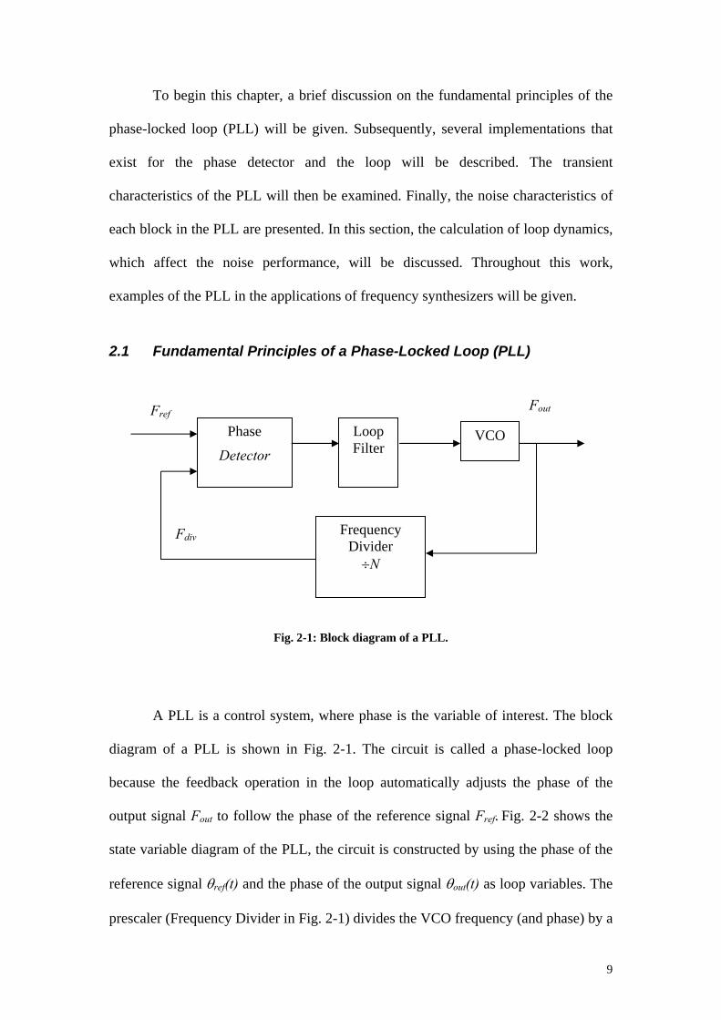
Fig. 2-1: Block diagram of a PLL.
A PLL is a control system, where phase is the variable of interest. The block
diagram of a PLL is shown in Fig. 2-1. The circuit is called a phase-locked loop
because the feedback operation in the loop automatically adjusts the phase of the
output signal Fout to follow the phase of the reference signal Fref. Fig. 2-2 shows the
state variable diagram of the PLL, the circuit is constructed by using the phase of the
reference signal θref(t) and the phase of the output signal θout(t) as loop variables. The
prescaler (Frequency Divider in Fig. 2-1) divides the VCO frequency (and phase) by a
Fout Fref
Fdiv
Phase
Detector
Loop Filter
Frequency Divider
÷N
VCO
10
division modulus of N. Let θdiv(t) be the phase of the output signal of the prescaler, the
following equation is obtained
θdiv(t) = θout(t)/N
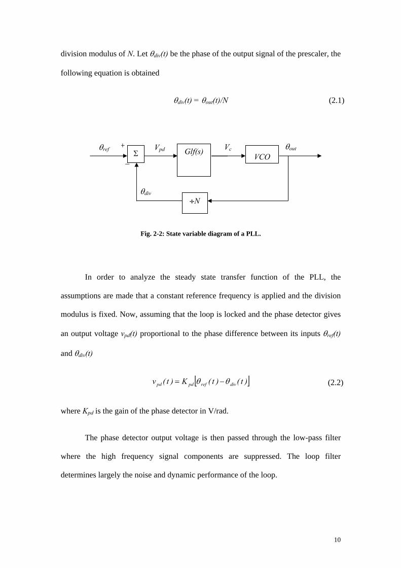
Fig. 2-2: State variable diagram of a PLL.
In order to analyze the steady state transfer function of the PLL, the
assumptions are made that a constant reference frequency is applied and the division
modulus is fixed. Now, assuming that the loop is locked and the phase detector gives
an output voltage vpd(t) proportional to the phase difference between its inputs θref(t)
and θdiv(t)
[ ])t()t(K)t(v divrefpdpd θθ −=
where Kpd is the gain of the phase detector in V/rad.
The phase detector output voltage is then passed through the low-pass filter
where the high frequency signal components are suppressed. The loop filter
determines largely the noise and dynamic performance of the loop.
Vc Vpd _
+ Σ
θout θref
θdiv
Glf(s)
÷N
VCO
(2.2)
(2.1)

11
An ideal voltage-controlled oscillator (VCO) generates a periodic output
whose frequency is a linear function of the control voltage vc and is given by
cvcofrout vK ×+= ωω
where ωfr is the free running frequency of the VCO and Kvco is the gain of the VCO
specified in rad/s/V. Since frequency is the derivative of phase, the VCO operation
can be described as
(t)vKdt
(t)dθcvco
out ⋅=
Taking the Laplace transform, it leads to
ssVK
s cvcoout
)()(
⋅=θ
Fig. 2-3: Linear time-invariant phase-model of the PLL.
If the signals around the loop are interpreted by their phases, the small-signal
noise behavior of the loop can be explored by linearizing the components and
evaluating the transfer functions. Fig. 2-3 shows the linear time-invariant (LTI) phase-
(2.5)
(2.4)
(2.3)
θdiv
θpd θvco
_
+ Σ
θout θref Kpd
÷N
+ +
Σ
+ +
Σ
θlf
F(s) +
+ Σ Kvco/s
+
+ Σ

12
model of the PLL. The forward gain is equal to ( ) sKsFKsG vcopd ××=)( , while the
feedback gain is equal to H(s)= 1/N. Hence, the open loop gain OL(s) is obtained as
sNK
sNKsFK
sHsGsOL Fvcopd
⋅=
⋅
⋅⋅=⋅=
)()()()(
where KF is the forward gain of the PLL and has unit of s-1. Equation (2.6) is useful to
study the operation of the PLL, such as the step response and the stability of the
system.
2.2 Transient Characteristics
In this section, the dynamic behavior of the loop when it is subjected to a
phase step or a frequency step in the reference frequency will be examined. Then the
startup behavior of the loop will be discussed.
2.2.1 Tracking
Equation (2.7) represents a phase step with a magnitude of ∆θ being applied
to the reference signal. The assumptions are made that the loop is in lock state and the
phase error is sufficiently small to justify an assumption of linearity.
θ∆θ )t(u)t(ref =
where u(t) is the unit step function. Applying the Laplace transform, equation (2.7)
becomes
ssref θθ ∆=)(
(2.7)
(2.8)
(2.6)

13
For t approaching infinity, the final value theorem of the Laplace transform
states
)s(s)t(st
θθ0
limlim→∞→
=
Therefore, the resulting steady state phase error for a first-order loop is
0])/(1
1[lim])(1
1)([lim00, =
+⋅
∆⋅=
+⋅⋅=
→→ NsKss
sGHss
Fsrefssserr
θθθ
It can be seen from the above equation that the PLL will reduce any phase
error to zero if given sufficient time.
If the input frequency changes with a step size of ∆ω, the input phase equals
θref(t) = t×∆ω. This situation appears when the division modulus in synthesizer is
changed. The resulting steady-state phase error is
pFFssserr K
NNsKs
sω
ωωωθ ∆=
⋅∆=
+⋅
∆⋅=
→]
)/(11[lim 20,
where ωp is the loop bandwidth in radians/sec, which is defined as the frequency
where the open loop gain is equal to one. In a system such as GSM, the local
oscillator (LO) has to switch from the receive channel to the transmit channel or
switch from one frequency band to another frequency band. The switching time
requirement must satisfy the GSM’s system specifications. This switching time TE is
the time a PLL takes to settle the new output frequency to be within a specified
accuracy E. In order to calculate TE, the following equation is used [28]
)s(sss
s)s(GH)s()s(
ppreferr ω
ω∆ω
ω∆θθ+⋅
=+
⋅=+
⋅= 211
(2.9)
(2.10)
(2.11)
(2.12)

14
Equation (2.12) in time-domain can be obtained as
)e()t( t
perr
pω
ωω∆θ −−⋅= 1
The final frequency is obtained after an exponential behavior with a time
constant τp = 1/ωp. For E = 1e-6, the switching time TE is given by [39]
ppE f
.ET 22ln=−=
ω
For a loop bandwidth fp of 3.3 kHz, the switching time TE is equal to
0.667msec. In GSM, for a frequency step of about 100 MHz, the settling time must be
done within 10msec for E = 1e-6 [28].
2.2.2 Acquisition
During startup, the PLL is initially in an unlocked condition, the process of
achieving lock state is called acquisition. Since acquisition is inherently a non-linear
process, its qualitative analysis is beyond the scope of this work. In this work, some
descriptive analysis will be done, more information can be found in [29]-[30].
If the initial VCO frequency is close enough to N×Fref, the PLL will lock up
with just a phase transient. The frequency range over which no cycles will be missed
before lock is obtained, is called the lock range, ∆ωL. If a reference frequency outside
the lock range is applied, the pull-in process will be slower. The normal operation of
the PLL is generally restricted to the lock range.
The pull-in range, ∆ωPI, describes the PLL in a dynamic state or an acquisition
mode. The pull-in range is the range within which a PLL will always become locked
(2.13)
(2.14)

15
through the acquisition process [31]. If the reference frequency is outside the pull-in
range, the PLL will not be able to lock onto the reference signal.
The hold range, ∆ωH, describes the PLL in a static or locked state. The PLL is
initially locked with reference signal. If the reference signal’s frequency changes too
much, the PLL will lose lock at the edge of the hold-in range. The PLL is
conditionally stable within the hold-in range [31]. The hold-in range is larger than
both above defined ranges. As will be discussed in Section 2.3.1, the linear
approximation of the phase error due to a frequency offset is shown to be θres,ss =
∆ω/KF. However, a real phase detector does not have an infinite linear range. For a
sinusoidal-characteristic phase detector, the true expression should be sinθres,ss =
∆ω/KF [28]. Since the sine function cannot exceed unit magnitude, there is no solution
for ∆ω > KF. The hold-in range therefore equals ∆ω = ±KF. Other types of phase
detector, for example the charge pump phase-frequency detector, have a larger linear
range and can therefore extend the hold-in range. However, these definitions are only
valid as long as the limit is set by the phase detector and not by some other
nonlinearities, such as the clipping in an operational amplifier (op-amp) or the VCO
frequency tuning range.
2.3 Phase Detector and Loop Filter
This section will describe the phase detector and loop filter. Various
implementations of phase detectors will be discussed. Then, the transfer
characteristics of the loop filter will be discussed. Finally, the calculation of an
optimum loop bandwidth will be presented. More information can be found in [29]-
[34].
16
2.3.1 Phase Detector
In this section, several representative phase detectors will be described. Phase
detectors can be classified into three major categories: analog phase detector, digital
phase detector, and phase-frequency detector. Firstly, the analog phase detector or
multiplier generates a DC component, which is dependent on the phase difference of
input signals. The DC component is used for phase difference detection. Secondly,
digital phase detector, such as the EXOR and the flip-flop phase detector, detects the
phase difference of the input signals based on their zero crossing points. Thirdly, the
phase-frequency detector is a sequential circuit, and it provides a frequency sensitive
signal to improve the acquisition when the loop is out of lock.
2.3.1.1 Multiplier
A multiplier acts as a phase detector through the trigonometric identity
)BA()BA()B()A( ++−= sin21sin
21cossin
If the input signals to the multiplier are v1 = A1sin(ω1t + θ1) and
v2 = A2cos(ω2t + θ2), the multiplier output signal will be
])(sin[])(sin[21
2121212121
21
θθωωθθωω ++++−+−⋅⋅⋅=
⋅⋅=
ttAAA
vvAv
d
dd
where Ad is the constant associated with the multiplier.
At phase lock, both frequencies are the same and the DC component of the
phase detector output equals 0.5×Ad×A1×A2×sin(θ1-θ2). This component indicates the
phase difference between the two signals. Various unwanted signal components are
(2.15)
(2.16)

17
also present at the output, such as the sum of the two input frequencies. The loop filter
will remove these unwanted signal components. One of the common implementation
of the multiplier phase detector is the Gilbert multiplier [30].
2.3.1.2 EXOR Gate
Fig. 2-4 shows the EXOR gate phase detector. The operation of an EXOR gate
phase detector is similar as an over-driven multiplier circuit and it has triangular
phase detector characteristics. However, square wave inputs of 50% duty cycle are
recommended for the EXOR phase detector. For other duty cycles, the detection range
may be significantly reduced. In addition, it is possible to have the same output
voltage for two different phase errors [120]. The output waveforms for inputs A and B
are shown in Fig. 2-5. The average value C of the output waveform is proportional to
the phase difference between the input signals. The phase detector transfer
characteristic is shown in Fig. 2-6.
Fig. 2-4: EXOR gate phase detector.
C
A
B

18
Fig. 2-5: The operation of an EXOR gate phase detector.
Fig. 2-6: The transfer characteristics of an EXOR gate phase detector.
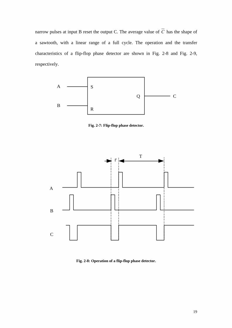
2.3.1.3 Flip-Flop Phase Detector
An edge-sensitive set-reset (SR) type of flip-flop can be used to detect the
phase difference of pulse trains, which do not have 50% duty cycle. The flip-flop
phase detector is shown in Fig. 2-7. Narrow pulses at input A set the output C, while
A
B
⊕ C=A B
τ T
0 0.5 1
/T τ
C
19
narrow pulses at input B reset the output C. The average value of C has the shape of
a sawtooth, with a linear range of a full cycle. The operation and the transfer
characteristics of a flip-flop phase detector are shown in Fig. 2-8 and Fig. 2-9,
respectively.
Fig. 2-7: Flip-flop phase detector.
Fig. 2-8: Operation of a flip-flop phase detector.
A
B
C
τ T
S
R
Q
A
B
C

20
Fig. 2-9: Transfer characteristics of a flip-flop phase detector.
2.3.1.4 Phase Frequency Detector
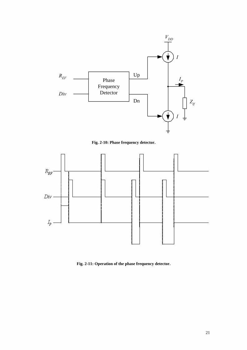
The phase frequency detector (PFD) has an unlimited pull-in range [34],
which is an advantage over the EXOR, flip-flop and multiplier phase detector. The
PFD is usually implemented together with a charge pump, as shown in Fig. 2-10. The
PFD has two outputs, Up and Dn, which open or close the two current sources of the
charge pump. The output current is then converted to a voltage across the impedance
Zlf.
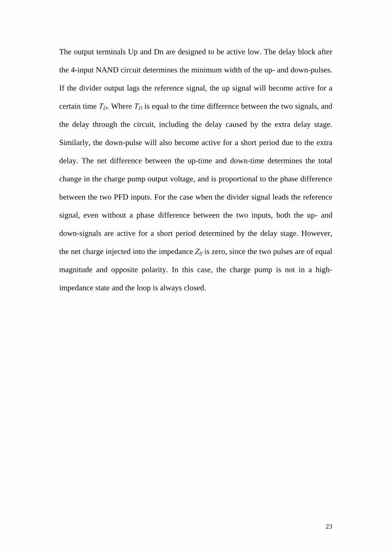
The operation of the PFD is shown in Fig. 2-11. The PFD has two inputs, the
reference signal REF and the feedback signal from the divider Div. The reference pulse
causes the output to change to a positive direction, unless the output is already
positive, in which case the pulse has no effect on the output. Similarly, the loop’s
divider output causes a negative transition unless the output is already negative. The
transfer characteristics of the PFD are plotted in Fig. 2-12 and have a linear phase
range of 4π.
0 0.5 1
/T τ
C
21
Fig. 2-10: Phase frequency detector.
Fig. 2-11: Operation of the phase frequency detector.
I
I
VDD
Zlf
IPREF
Div
Up
Dn
PhaseFrequencyDetector

22
Fig. 2-12: Transfer characteristics of the phase frequency detector.
The PFD in Fig. 2-10 suffers from a “dead zone”, which arises from the
crossover distortion, where changes in gain occurring near the zero phase error [35].
If both the reference pulse and the divider pulse appear at the same time, none of the
outputs becomes active and the charge-pump output is in high-impedance state. Even
if the phase difference changes slightly, the phase detector will not respond
immediately since it requires some finite time for the Up and Dn pulses to propagate
through the circuit. Therefore, the charge pump keeps its high impedance state
although there is a slight phase difference. Hence, the phase detector characteristic
actually has a flat response, which is known as dead zone, near the zero phase
difference.
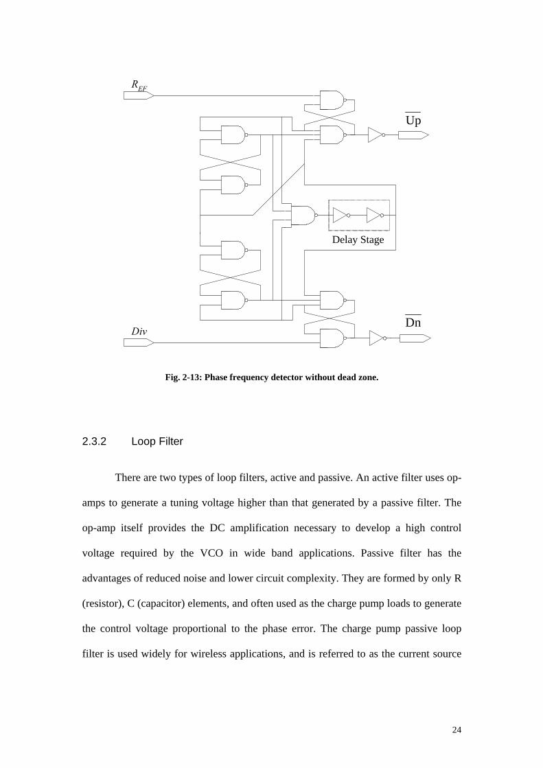
Giving a fixed minimum width to both the charge pump pulses can solve the
problem of the dead zone. Fig. 2-13 shows a PFD circuit that is free of dead zone [36].
0 0.5 1/Tτ
-1 -0.5
C
23
The output terminals Up and Dn are designed to be active low. The delay block after
the 4-input NAND circuit determines the minimum width of the up- and down-pulses.
If the divider output lags the reference signal, the up signal will become active for a
certain time TD. Where TD is equal to the time difference between the two signals, and
the delay through the circuit, including the delay caused by the extra delay stage.
Similarly, the down-pulse will also become active for a short period due to the extra
delay. The net difference between the up-time and down-time determines the total
change in the charge pump output voltage, and is proportional to the phase difference
between the two PFD inputs. For the case when the divider signal leads the reference
signal, even without a phase difference between the two inputs, both the up- and
down-signals are active for a short period determined by the delay stage. However,
the net charge injected into the impedance Zlf is zero, since the two pulses are of equal
magnitude and opposite polarity. In this case, the charge pump is not in a high-
impedance state and the loop is always closed.
24
Fig. 2-13: Phase frequency detector without dead zone.
2.3.2 Loop Filter
There are two types of loop filters, active and passive. An active filter uses op-
amps to generate a tuning voltage higher than that generated by a passive filter. The
op-amp itself provides the DC amplification necessary to develop a high control
voltage required by the VCO in wide band applications. Passive filter has the
advantages of reduced noise and lower circuit complexity. They are formed by only R
(resistor), C (capacitor) elements, and often used as the charge pump loads to generate
the control voltage proportional to the phase error. The charge pump passive loop
filter is used widely for wireless applications, and is referred to as the current source
REF
Div
Delay Stage
Up
Dn

25
loop filter [37]. This is in contrast to the voltage source loop filter for an active loop
filter.
2.3.2.1 Charge Pump PLL
Fig. 2-14 shows a 3rd order, type-2 charge-pump PLL. The phase detector’s
current source outputs pump charge into the loop filter, to produce the VCO’s control
voltage. Compared to a 2nd order charge-pump PLL, the extra capacitor C1 in the 3rd
order PLL is added to smooth out the discrete voltage steps at the control port of the
VCO due to the instantaneous changes in the charge pump current output. At each
cycle of the PFD, a pump current Icp is driven into the filter impedance with an
instantaneous voltage jump of IcpR2. The corresponding frequency jump is
pcpvco RIK ωπω ×=××=∆ 22
which is generally larger than the average frequency increment per cycle [38].
Fig. 2-14: A 3rd order, type-2 charge pump PLL filter.
C 1 C 2
R 2
From Charge Pump, I cp (t)
To VCO
(2.17)
26
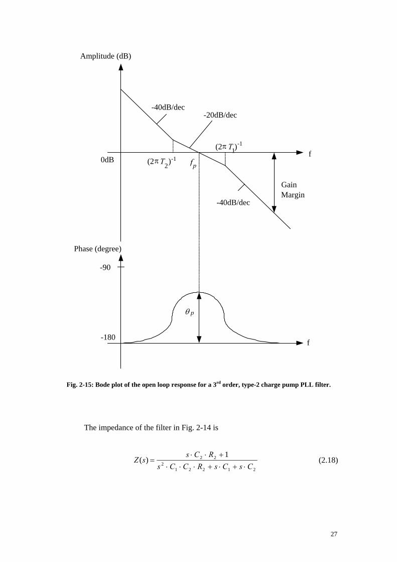
The filter can be designed based on the open loop gain bandwidth and the
phase margin required. Positioning the point of minimum phase shift at the unity gain
frequency of the open loop response as shown in Fig. 2-15 ensures the loop stability.
The phase relationship between the pole and zero also allows the determination of the
loop filter component values. The phase margin θp is defined as the difference
between 180° and the phase of the open loop transfer function at the unity-gain
frequency fp. The phase margin is chosen between 30° and 70° for most applications
[39]. The larger the phase margin, the more stable the loop. However, the transient
response is slower and requires a longer switching time. A loop with a low phase
margin may still be stable but could exhibit oscillator problems associated with an
undamped loop, such as longer switching time and increased noise. A phase margin of
45° is a good compromise between desired stability and the other generally undesired
effects.
27
Fig. 2-15: Bode plot of the open loop response for a 3rd order, type-2 charge pump PLL filter.
The impedance of the filter in Fig. 2-14 is
212212
22 1)(
CsCsRCCsRCs
sZ⋅+⋅+⋅⋅⋅
+⋅⋅= (2.18)
Phase (degree)
Amplitude (dB)
(2 T 2) -1π
-40dB/dec
0dB
-20dB/dec
-40dB/dec
Gain Margin
-180
-90
(2 T 1) -1 π
p θ
p f f
f
28
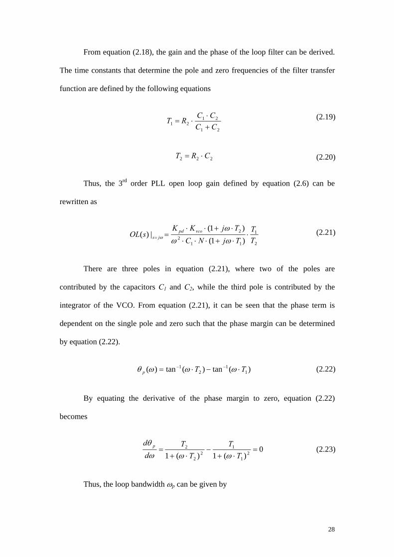
From equation (2.18), the gain and the phase of the loop filter can be derived.
The time constants that determine the pole and zero frequencies of the filter transfer
function are defined by the following equations
21
2121 CC
CCRT
+⋅
⋅=
222 CRT ⋅=
Thus, the 3rd order PLL open loop gain defined by equation (2.6) can be
rewritten as
2
1
112
2
)1()1(
|)(TT
TjNCTjKK
sOL vcopdjs ⋅
⋅+⋅⋅⋅
⋅+⋅⋅== ωω
ωω
There are three poles in equation (2.21), where two of the poles are
contributed by the capacitors C1 and C2, while the third pole is contributed by the
integrator of the VCO. From equation (2.21), it can be seen that the phase term is
dependent on the single pole and zero such that the phase margin can be determined
by equation (2.22).
)(tan)(tan)( 11
21 TTp ⋅−⋅= −− ωωωθ
By equating the derivative of the phase margin to zero, equation (2.22)
becomes
0)(1)(1 2
1
12
2
2 =⋅+
−⋅+
=T
TT
Tdd p
ωωωθ
Thus, the loop bandwidth ωp can be given by
(2.19)
(2.20)
(2.21)
(2.22)
(2.23)
29
121 )( −⋅= TTpω
Sometimes, the 3rd order structure does not provide sufficient rejection to the
reference spur. The reference spur is caused by the current switching noise in the
dividers and that in the charge pump at the reference rate Fref. In wireless
communications, the phase detector operation frequency is generally a multiple of the
RF channel spacing. These spurious sidebands can cause noise in adjacent channels.
This is usually the case in the TDMA digital cellular standards, such as GSM or IS-54.
A narrow loop filter has advantage of better attenuation of the reference spur, but the
requirement of the sub-milliseconds switching between channels makes a relatively
wide loop filter mandatory.
One solution is to use an additional low pass pole for more attenuation of the
unwanted spur. The use of a passive loop filter eliminates the noise contributions from
the op-amp in an active filter. This is critical due to the strict phase error and
integrated phase noise requirements. For example, the integrated phase noise
requirement for the SONET’s OC-192 specification is 1 ps root-mean-square value
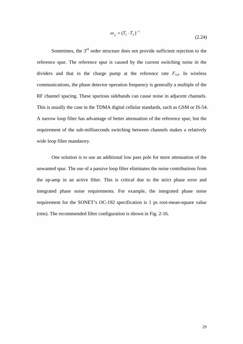
(rms). The recommended filter configuration is shown in Fig. 2-16.
(2.24)
30
Fig. 2-16: A 4th order, type-2 charge pump PLL filter.
The additional pole must be lower than the reference frequency to
significantly attenuate the reference spur, but must be at least 5 times higher than the
loop bandwidth to maintain the loop stability [37]. The additional filter time constant
can be defined as
1333 )( −⋅= CRT
The bode plot of the open loop response for the 4th order charge pump PLL is
shown in Fig. 2-17.
(2.25)
C1
C2
R2
From Charge Pump ,Icp(t)
To VCO
C3
R3

31
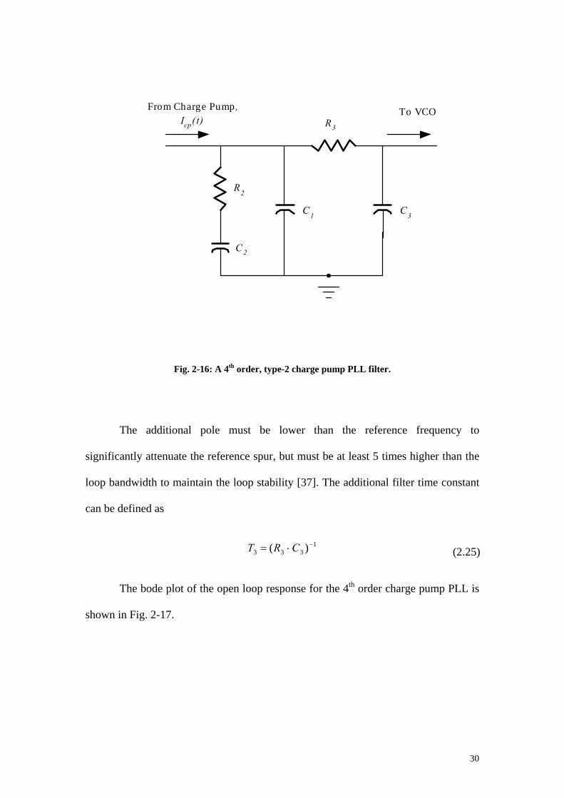
Fig. 2-17: Bode plot of the open loop response for a 4th order, type-2 charge pump PLL.
A charge pump PLL for the GSM applications has been simulated to illustrate
the open loop response of the 3rd order and 4th order charge pump PLLs. Fig. 2-18
shows the filter response and the PLL open loop gain for the 3rd and 4th order cases.
The 3rd order loop filter response shows a 20 dB/dec slope due to the integrator from
the loop filter, flattening out at the zero frequency which is equal to 1/(2πT2) = 4.5
kHz in the example. For the 4th order loop filter, the response again drops at the rate
of 20 dB/dec starting at the pole frequency of 1/(2πT1) = 54 kHz. The slope of the
Phase (degree)
Amplitude (dB)
(2 T 2)-1π
-40dB/dec
0dB
-20dB/dec
-40dB/dec
Gain Margin
-180
-90
(2 T 1)-1π (2 T 3)-1 π
-60dB/dec
p θ
p f f
f

32
open loop gain for the both 3rd and 4th order charge pump PLL is 20 dB/dec more than
their respective loop filters gain due to the integrator from the VCO. The slope before
the zero is 40 dB/dec, it changes to 20 dB/dec after the zero and then changes back to
40 dB/dec after the first pole. For the 4th order loop filter, the slope changes to 60
dB/dec after the second pole at the frequency of 1/(2πT3) = 1 MHz.
Fig. 2-18: Loop filter gain and PLL open loop gain for 3rd and 4th order charge pump PLLs.
The phase responses are shown in Fig. 2-19. For both the 3rd and 4th order
filters, the phase shift at the zero frequency is –90o. The phase approaches 0o after the
zero, and then drops back to –90o after the first pole. For the 4th order filter, the phase
approaches –180o after the second pole. The open loop phase for both cases differs
from their respective loop filters phase by –90o. For both the 3rd and 4th order loop
filters, the phase starts at –180o. It approaches –90o after the zero, and returns to –180o
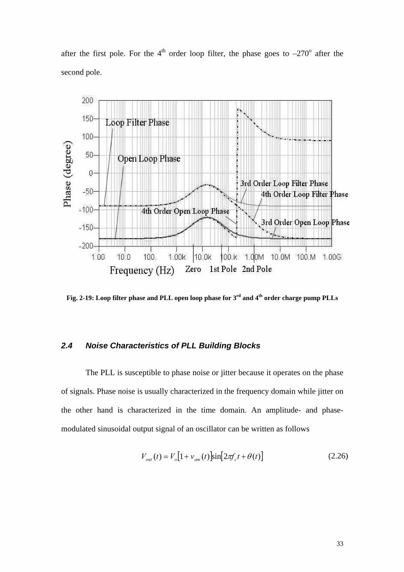
33
after the first pole. For the 4th order loop filter, the phase goes to –270o after the
second pole.
Fig. 2-19: Loop filter phase and PLL open loop phase for 3rd and 4th order charge pump PLLs
2.4 Noise Characteristics of PLL Building Blocks
The PLL is susceptible to phase noise or jitter because it operates on the phase
of signals. Phase noise is usually characterized in the frequency domain while jitter on
the other hand is characterized in the time domain. An amplitude- and phase-
modulated sinusoidal output signal of an oscillator can be written as follows
[ ] [ ])(2sin)(1)( ttftvVtV camoout θπ ++= (2.26)
34
where Vo is the amplitude, fc is the carrier frequency, vam(t) is the amplitude-
modulation (AM) component and θ(t) is the phase-modulation (PM) component. The
AM component will be omitted since only the phase noise is concerned.
[ ])(2sin)( ttfVtV coout θπ +=
For a sinusoidal-angle modulation with a rate of fm
t)πf(f∆fθ(t) c
m
2sin⋅=
Let β = ∆f/fm, equation (2.27) becomes
[ ])2(sin2sin)( tftfVtV mcoout πβπ +=
where fm is the modulation frequency, ∆f is the peak frequency-modulation deviation,
and β is the modulation index. For small-angle modulation, where β < 1,
trigonometric identities can be applied. This leads to
[ ] [ ] tfftfftf(VtV mcmccoout )(2sin)(2sin5.0)2sin)( −−++= ππβπ
From this expression, it can be concluded that a small-angle deviation gives
rise to sidebands on each side of the carrier with an amplitude of β/2. Therefore,
phase noise can be regarded as an infinite number of single FM sidebands [21].
Phase noise indicates the error or random deviation of the frequency of the
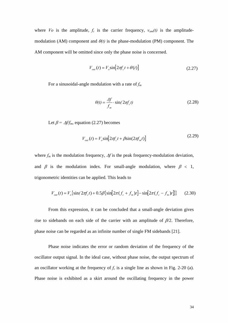
oscillator output signal. In the ideal case, without phase noise, the output spectrum of
an oscillator working at the frequency of fc is a single line as shown in Fig. 2-20 (a).
Phase noise is exhibited as a skirt around the oscillating frequency in the power
(2.30)
(2.29)
(2.28)
(2.27)
35
spectrum. Phase noise is defined as the noise power in a unit bandwidth at an offset of
∆f from the center frequency fc divided by the carrier power as shown in Fig. 2-20 (b).
Fig. 2-20: Output spectrum of (a) ideal oscillator; (b) actual oscillator.
Phase noise can be measured in different ways. One way is to use a spectrum
analyzer where the total power of the signal would firstly be measured. Since the
noise is small, this is essentially equal to the carrier power [21]. Then the phase noise
power would be measured with the receiver tuned to a particular offset ∆f from the
carrier. The ratio of these two measurement results, expressed in decibels, is the
normalized power spectral density (PSD) in one sideband at a frequency offset ∆f
referred to the carrier. This is known as the single-sideband (SSB) phase noise relative
to the carrier level, L(∆f), expressed in decibels as dBc/Hz. A plot of the phase noise
as function of the offset is commonly shown in data sheets in order to characterize
oscillators and frequency synthesizers.
dBc 1 Hz Bandwidth
f∆
fffc
f c
Power (dB)Power (dB)
(a) (b)
36
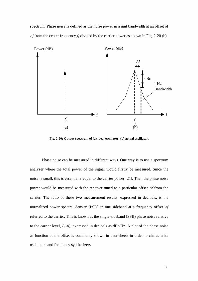
Another method is to demodulate the signal with a phase demodulator. The
output of the phase demodulator is the baseband phase noise and can be analyzed with
a low frequency spectrum analyzer, with a 1Hz resolution-bandwidth filter. The
resulting plot as a function of the baseband offset frequency is the double-sided phase
noise spectrum, S(∆f), expressed in dBc/Hz. As shown in Fig. 2-21, the double-
sideband phase noise is 3 dB more than that of the SSB phase noise.
Fig. 2-21: Single sideband and double sideband phase noise.
In the case where the noise of the PLL circuit is lower than that of the analyzer,
there are alternative phase noise measurement systems. Phase noise can be measured
by comparing the PLL signals in quadrature to a signal source with a noise level
lower than that of the PLL signals and it is calculated at the output of the mixer using
an FFT analyzer [27]. A new method to measure phase noise is the delay line method
[27], which implements a frequency discriminator by mixing the signal with its
delayed replica using a coaxial cable.
L( f) (dB) ∆ S( f) (dB)∆
f ∆
Double Sideband Phase Noise
f ∆
Single Sideband phase Noise
3dB

37
If the input signal or the building blocks of a PLL exhibit noise, the output
signal will also suffer from noise. All loop components, which include the VCO, LF,
phase detector and frequency divider, may contribute to phase noise [22]. The
objectives are to understand how the spectrum of a given noise source is shaped as it
propagates to the output and its effects on the total phase noise. Four important noise
sources will be examined: (1) the VCO, (2) the reference signal, (3) the frequency
divider, and (4) the LF. Note that the noise contribution of the phase detector is not
being considered here. The reason is that at a low operating frequency, phase detector
can be designed to have negligible effects on the overall phase noise of the PLL [23].
Fig. 2-3 can also be used to describe the relationship among individual phase
noise sources, where noise generated by the VCO, noise included in the reference
signal, noise generated by the frequency divider and the loop filter noise are
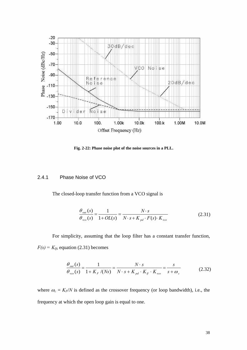
represented by θvco, θref, θdiv and θlf, respectively. The typical phase noise plot of the
VCO noise, reference signal noise and frequency divider noise for a frequency
synthesizer in the GSM application is illustrated in Fig. 2-22 [21]. The loop filter
noise will be discussed in Section 2.4.4 in detail.
38
Fig. 2-22: Phase noise plot of the noise sources in a PLL.
2.4.1 Phase Noise of VCO
The closed-loop transfer function from a VCO signal is
vcopdvco
out
KsFKsNsN
sOLss
⋅⋅+⋅⋅
=+
=)()(1
1)()(
θθ
For simplicity, assuming that the loop filter has a constant transfer function,
F(s) = Klf, equation (2.31) becomes
cvcolfpdFvco
out
ss
KKKsNsN
NsKss
ωθθ
+=
⋅⋅+⋅⋅
=+
=)/(1
1)()(
where ωc = KF/N is defined as the crossover frequency (or loop bandwidth), i.e., the
frequency at which the open loop gain is equal to one.
(2.32)
(2.31)
39
Equation (2.32) shows that the noise transfer function from the VCO to the
output has a high pass characteristic. Noise at high frequencies passes without being
attenuated, because the feedback action of the loop is too slow to suppress these noise
components. Note that although it is assumed that the loop filter has a constant
transfer function, the analysis is applicable for higher order loop filter.
A 4th order charge pump PLL frequency synthesizer for the GSM application
has been simulated to illustrate the noise properties of the PLL. The Leeson-Culter
phase noise model [24]-[26], is used for modeling the VCO noise in the example. The
spectral density of a VCO, Svco(∆ω), is found to be
])2
(1)[1(2)( 203
ωω
ωω
ω∆
+∆
+⋅=∆L
c
svco QP
FkTS
where F is an empirical parameter often called the device excess factor, k is the
Boltzmann’s constant, T is the absolute temperature, Ps is the average power
dissipated in the resistive part of the tank, ω0 is the oscillation frequency, QL is the
effective quality factor of the tank, ∆ω is the offset from the carrier and ωc3 is the
frequency of the corner between the 1/f3 and 1/f2 regions. Let A = FkT/Ps, equation
(2.33) can be rearranged as
AAQA
QA
S c
LL
cvco +
∆+
∆+
∆∆=∆ )())(
4())(
4()( 320
220
23
ωω
ωω
ωω
ωω
ω
Let k3 = Aωc3ω02/(4QL
2), k2 = Aω02/(4QL
2), k1 = Aωc3, and k0 = A, equation
(2.34) can be simplified to be
01
22
33)( k
kkkSvco +
∆+
∆+
∆=∆
ωωωω (2.35)
(2.34)
(2.33)

40
One of the advantages of equation (2.35) is its close resemblance to the actual
phase noise characteristics of the oscillator, which will be discussed in detail in the
next chapter. Another advantage is that the four coefficients of equation (2.35) can be
manually adjusted to yield the correct numerical value of VCO phase noise at all
offset frequencies. The coefficients k3, k2, k1 and k0 of the VCO noise in Fig. 2-22 are
experimentally determined using asymptotic lines with a slope of –30 dB/dec, -20
dB/dec, -10 dB/dec and 0 dB/dec. The values were obtained to be 100.7, 10-3, 10-14.5
and 10-15.5, respectively. For example, using equation (2.35), the calculated phase
noise at 1 kHz offset is
2098210log10 3 .)(Svco −=× dBc/Hz
which agrees with value of VCO noise at 1 kHz offset in Fig. 2-22.
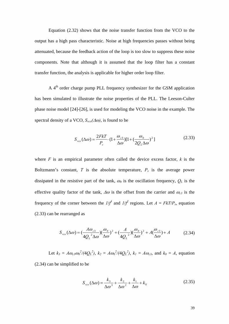
The closed loop transfer function of the VCO noise is shown in Fig. 2-23. By
multiplying the square of the closed loop transfer function of the VCO given in
equation (2.32) with equation (2.35), the contribution of the VCO noise to the total
output noise of a PLL can be obtained as
2_ |
)()(
|)*()(ss
SSvco
outvcoVCOT θ
θωω ∆=∆
Fig. 2-24 shows that while the VCO is very noisy close to the carrier, the noise
is significantly attenuated within the loop bandwidth, which is 3.3 kHz for this
example. The magnitude of the VCO closed loop transfer function determines the
amount of noise attenuation. On a close inspection of Fig. 2-24, the loop has a gain of
40 dB/dec from DC to the zero at 1.7 kHz. From the zero to the gain crossover
frequency at 3.3 kHz, the loop can reject the VCO noise by 20 dB/dec. The VCO has
(2.36)
(2.37)
41
a 30 dB/dec slope from DC to 5 kHz, where it changes to a 20 dB/dec slope. Close to
the gain crossover frequency, the VCO noise is increased by 30 dB/dec but the loop
can only reject noise by 20 dB/dec. Therefore, there exists a net increase of 10 dB/dec
in the total output noise. At the zero, the loop can reject the noise by 40 dB/dec. Thus,
taking into account the 30 dB/dec slope of the VCO noise, there is a net decrease of
10 dB/dec in the total output noise.
Fig. 2-23: Closed loop transfer function of the VCO noise.

42
Fig. 2-24: Effect of the PLL on VCO noise.
2.4.2 Phase Noise of Reference Input Signal
The closed-loop transfer function from a reference input signal is
vcopd
vcopd
ref
out
KsFKsNKsFKN
sOLG
ss
⋅⋅+⋅
⋅⋅⋅=
+=
)()(
)(1)()(
θθ
For simplicity, assuming that the loop filter has a constant transfer function,
F(s) = Klf, equation (2.38) becomes
c
c
vcopd
vcopd
ref
out
sN
KsFKsNKsFKN
ss
ωω
θθ
+⋅=
⋅⋅+⋅
⋅⋅⋅=
)()(
)()(
Equation (2.39) shows that the transfer function from the reference input
signal to the output signal has a low pass characteristic superimposed on a
(2.39)
(2.38)

43
multiplication with a factor N. Note that although it is assumed that the loop filter has
a constant transfer function, the analysis is applicable for higher order loop filter.
The reference input signal generally comes from a crystal oscillator, which has
typically a very high Q. Hence, the reference noise can be modeled according to the
phase noise plot of a crystal oscillator. According to equation (2.33), the phase noise
of an oscillator is a function of the quality factor Q or the bandwidth of the resonator.
The phase noise improves with a higher Q, or a narrower resonator bandwidth. A
lower 1/f corner also improves the noise performance. If a resonator has a low Q, as
typically in most inductive-capacitive (LC) oscillators, the 1/f corner is inside the
resonator bandwidth [21]. This results in a phase noise plot consisting of three
different regions, namely the flat noise region, the 1/f2 region and the 1/f3 region as
shown in Fig. 2-25(a). For a high Q resonator, the resonator bandwidth is smaller than
the 1/f corner. Therefore, after the flat region, the 1/f corner is reached first and then
the phase noise increases at a rate of 10 dB/dec, which is followed by the 1/f3 region
as shown in Fig. 2-25(b). However, the explanation is rather simplified since a more
accurate model will include four regions [21].
Similar to the VCO noise, the reference noise can be modeled by
01
22
33 k
kkk)(S ref +++=
ω∆ω∆ω∆ω∆
where the coefficients k3, k2, k1 and k0 of the reference noise in Fig. 2-22 are
experimentally determined using asymptotic lines with a slope of –30 dB/dec, -20
dB/dec, -10 dB/dec and 0 dB/dec and the values were obtained to be 10-7.8, 10-9.8, 10-
12.7 and 10-15.8, respectively.
(2.40)

44
Fig. 2-25: Phase noise plots (a) low Q; (b) high Q.
The closed loop transfer function of the reference noise is shown in Fig. 2-26.
By multiplying the square of the closed loop transfer function of the reference noise
given in equation (2.39) with equation (2.40), the contribution of the reference noise
to the total output noise of a PLL can be obtained as
2_ |
)()(
|)*()(ss
SSref
outrefREFT θ
θωω ∆=∆
Fig. 2-26 and Fig. 2-27 show that the magnitude of the closed loop transfer
function of the reference noise determines the amount of noise rejection. The
multiplied reference noise is the result of the reference noise multiplied by the
division ratio N of the divider, as shown in equation (2.39). The multiplied reference
noise is then modified by the closed loop transfer function of the reference noise,
denoted as reference noise modified by loop in Fig. 2-27. The loop can reject the
f -1 ∆ FkT/2P s
f/2Q f 1/f
L( f) (dB) ∆
f ∆
FkT/2P s
f/2Q f 1/f
L( f) (dB) ∆
f ∆
f -3 ∆
f -2 ∆
f -3 ∆
(a) (b)
(2.41)
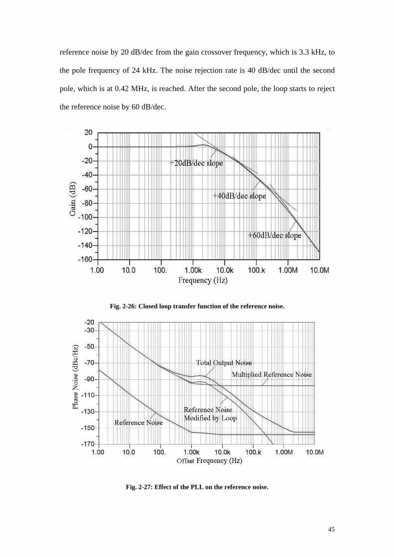
45
reference noise by 20 dB/dec from the gain crossover frequency, which is 3.3 kHz, to
the pole frequency of 24 kHz. The noise rejection rate is 40 dB/dec until the second
pole, which is at 0.42 MHz, is reached. After the second pole, the loop starts to reject
the reference noise by 60 dB/dec.
Fig. 2-26: Closed loop transfer function of the reference noise.
Fig. 2-27: Effect of the PLL on the reference noise.
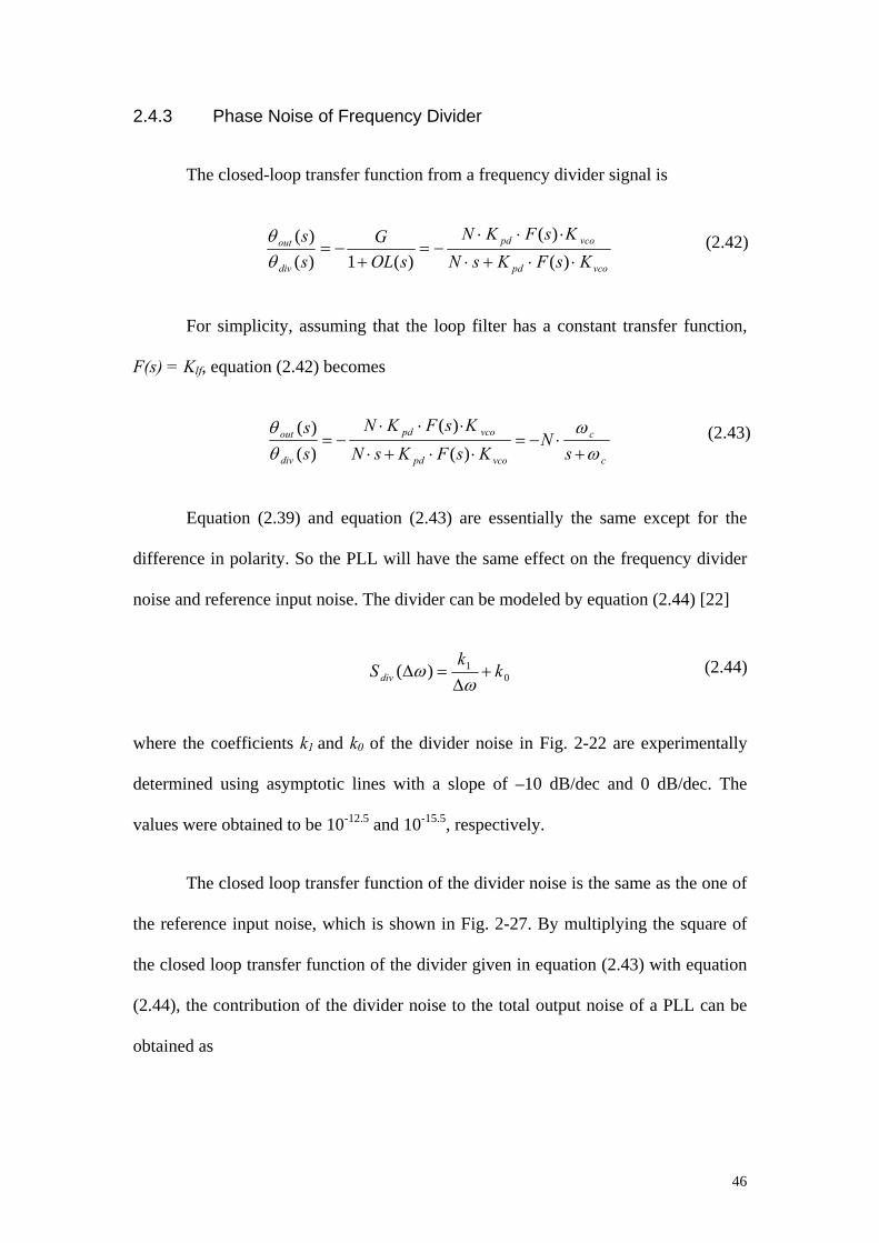
46
2.4.3 Phase Noise of Frequency Divider
The closed-loop transfer function from a frequency divider signal is
vcopd
vcopd
div
out
KsFKsNKsFKN
sOLG
ss
⋅⋅+⋅
⋅⋅⋅−=
+−=
)()(
)(1)()(
θθ
For simplicity, assuming that the loop filter has a constant transfer function,
F(s) = Klf, equation (2.42) becomes
c
c
vcopd
vcopd
div
out
sN
KsFKsNKsFKN
ss
ωω
θθ
+⋅−=
⋅⋅+⋅
⋅⋅⋅−=
)()(
)()(
Equation (2.39) and equation (2.43) are essentially the same except for the
difference in polarity. So the PLL will have the same effect on the frequency divider
noise and reference input noise. The divider can be modeled by equation (2.44) [22]
01)( k
kS div +
∆=∆
ωω
where the coefficients k1 and k0 of the divider noise in Fig. 2-22 are experimentally
determined using asymptotic lines with a slope of –10 dB/dec and 0 dB/dec. The
values were obtained to be 10-12.5 and 10-15.5, respectively.
The closed loop transfer function of the divider noise is the same as the one of
the reference input noise, which is shown in Fig. 2-27. By multiplying the square of
the closed loop transfer function of the divider given in equation (2.43) with equation
(2.44), the contribution of the divider noise to the total output noise of a PLL can be
obtained as
(2.43)
(2.42)
(2.44)

47
2_ |
)()(
|)*()(ss
SSdiv
outdivDIVT θ
θωω ∆=∆
The effect of the PLL on divider noise is shown in Fig. 2-28. The multiplied
divider noise is the result of the divider noise multiplied by the divider division ratio
N as shown in equation (2.43). The multiplied divider noise is then modified by the
divider closed-loop transfer function, which is denoted as the divider noise modified
by loop in Fig. 2-28. From equation (2.45), it is expected that the divider noise will
degrade by a factor of 10logN2 within the loop bandwidth. Thus the multiplied divider
noise with a divider’s division ratio of 1000 is 60dB more than the divider noise as
shown in Fig. 2-28. Similarly, the multiplied reference noise is 60dB more than the
reference noise as shown in Fig. 2-27. Since the reference noise and the divider noise
are non-correlated noise sources, it is possible to combine the effects of the reference
noise and divider noise by power summation as shown in Fig. 2-29.
Fig. 2-28: Effect of the PLL on the divider noise.
(2.45)

48
Fig. 2-29: Effect of the PLL on the divider noise and the reference noise.
2.4.4 Phase Noise of Loop Filter
The closed-loop transfer function from a loop filter noise signal is
vcopd
vco
lf
out
KsFKsNKN
ss
⋅⋅+⋅⋅
=)()(
)(θθ
If the loop filter has a 1st order passive filter function, F(s) = 1/(1+s/ωp),
equation (2.46) becomes
NKKssKs
ss
vcopdpp
vcop
lf
out
/)(
)()(
2 ⋅⋅++
⋅+−=
ωω
ωθθ
Equation (2.47) shows that the closed loop transfer function of the loop filter
noise has a band-pass characteristic. In a simple RC filter, the major noise source is
from the resistors. The noise power density for a resistor with the value of R, can be
modeled using Sres = 4kTR. Fig. 2-30 shows the contribution of the loop filter noise to
(2.47)
(2.46)
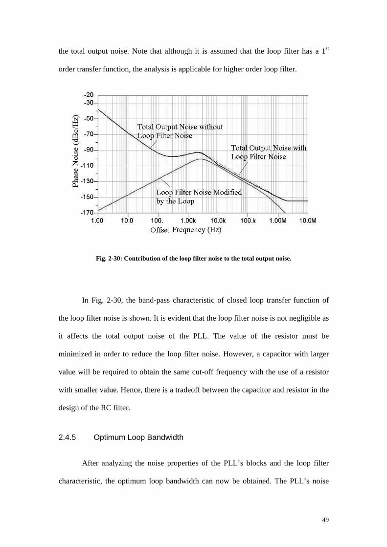
49
the total output noise. Note that although it is assumed that the loop filter has a 1st
order transfer function, the analysis is applicable for higher order loop filter.
Fig. 2-30: Contribution of the loop filter noise to the total output noise.
In Fig. 2-30, the band-pass characteristic of closed loop transfer function of
the loop filter noise is shown. It is evident that the loop filter noise is not negligible as
it affects the total output noise of the PLL. The value of the resistor must be
minimized in order to reduce the loop filter noise. However, a capacitor with larger
value will be required to obtain the same cut-off frequency with the use of a resistor
with smaller value. Hence, there is a tradeoff between the capacitor and resistor in the
design of the RC filter.
2.4.5 Optimum Loop Bandwidth
After analyzing the noise properties of the PLL’s blocks and the loop filter
characteristic, the optimum loop bandwidth can now be obtained. The PLL’s noise
50
sources can be separated into three categories as shown in Fig. 2-31, noise sources
outside the loop, noise sources inside the loop and noise source contributed by the
loop filter.
Fig. 2-31: Phase noise contributions in a PLL.
The VCO noise is said to be the noise source outside the loop because the
VCO noise is not modified by the loop outside the loop bandwidth. Inside the loop
bandwidth, the loop attempts to reject the noise. In order to achieve the most rejection
of VCO noise, the loop bandwidth should be as wide as possible and the zero
frequency should be placed as close to the unity gain frequency ωp as possible.
However, moving the zero closer to the gain crossover frequency will decrease the
phase margin and increase the peaking effect.
Both the reference noise and the divider noise are the noise sources inside the
loop because these noise sources are not modified by the loop inside the loop
Attenuation (dB)
(2 f ) π
0dB
p ω
Noise Inside the Loop
Noise Outside the Loop
Low Pass Response High Pass Response
LoopFilterNoise

51
bandwidth. Outside the loop bandwidth, the loop attempts to reject the noise. The
phase detector noise can also be included in this category. Making the loop bandwidth
narrower will increase the noise rejection inside the loop bandwidth. Moving the pole
closer to the gain crossover frequency will increase the noise rejection within the loop
but decrease the phase margin and increase peaking effect. Note that the loop filter
has a band-pass characteristic, so the loop filter noise is attenuated by both the noise
rejection inside and the noise rejection outside the loop bandwidth.
A rule of thumb to find the optimum loop bandwidth fopt for noise is where the
VCO noise curve intersects with the multiplied (N) sum of the reference noise and
divider noise [21]. Using equations (2.35), (2.40) and (2.44), the optimum loop
bandwidth fopt can be calculated from equation (2.48)
))()(()( 2optdivoprefoptvco StSNS ωωω ∆+⋅=
Using the same example as in Section 2.2, and supposing the division ratio N
is changed to 100 (N = 1000 in the previous example). The reference frequency is thus
changed to 10 MHz, which was 100 MHz. If the phase noise of the reference and the
divider remains unchanged, the new total output noise plot is shown in Fig. 2-32.
Note that there is a large bump on the total output noise plot from 1 kHz to 8 kHz. In
this region, the contribution of the multiplied reference noise and divider noise is
about 13dB lower than the total output noise. The total output noise at this region is
mostly from the VCO noise. This shows that the original loop bandwidth of 3.3 kHz
is not optimized. By applying equation (2.48), the optimum loop bandwidth, fopt can
be derived to be 8.5 kHz. The new noise plot using the fopt of 8.5 kHz is shown in
Fig. 2-33. It is shown that the total output noise has been improved by about 10dB in
the region from 1 kHz to 8 kHz, which is due to the wider loop bandwidth. The loop
(2.48)

52
is now able to reject more VCO noise in this region. Note that noise in the region
from 8 kHz to 20 kHz has increased by about 1dB. This is because less reference
noise and divider noise is being attenuated in this region due to the wider loop
bandwidth.
Fig. 2-32: Phase noise contribution in a PLL with N = 100 and loop bandwidth of 3.3 kHz.
Fig. 2-33: Phase noise contribution in a PLL with N = 100 and loop bandwidth of 8.5 kHz.

53
2.5 Summary
In this chapter, a brief overview of the PLL was presented. The total output
noise is critical to the performance of the PLL and is determined by the noise sources
presented in PLL blocks and by their closed loop transfer functions. The order and
type of the loop as well as the loop bandwidth determine the transient performance of
the PLL. Various types of phase detectors along with their advantages and
disadvantages have been discussed. An analysis of the 3rd order and the 4th order
charge pump PLL was presented, and the optimum loop bandwidth was shown. The
design of VCO will be presented in the following chapter.

54
CHAPTER 3
Voltage-Controlled Oscillator
An oscillator can be described as a positive feedback system and it amplifies
its own noise at a selected frequency ω0, as shown in Fig. 3-1.
Fig. 3-1: Feedback diagram of an oscillator.
The transfer function of the oscillator is
)(1)(
)()(
sGsG
sVsV
Ain
out
−==
From equation (3.1), it can be concluded that the closed loop gain will
approach infinity under the following conditions: (1) the open loop gain is equal to
unity, i.e. ( ) 1=SG , and (2) the total phase shift of the loop is equal to 0o, i.e.
( ) oSG 0=∠ , which are called the Barkhausen’s Criteria.
Σ
Vin(s)
Vout(s)
++ G(s)
(3.1)

55
In an environment with the existence of noise at all frequencies, the
Barkhausen’s Criteria is satisfied only with the noise at a specific frequency ω0. When
the oscillation is properly started, the noise signal at frequency ω0 is amplified and
increased till the amplifying devices are saturated. Hence, the stable oscillation is
maintained. In order to ensure the startup of the oscillation in presence of temperature
and process variations, the small signal loop gain is typically chosen to be 2-3 times
of the required value.
In most applications, it is required that the oscillator to be tunable, where the
output frequency is a function of a control input. Thus, a VCO can be described by
cvcofrout vK ×+= ωω
where ωfr is the free running frequency of the VCO, vc is the control voltage of the
VCO and Kvco is the gain of the VCO specified in rad/s/V. A voltage signal with
magnitude of Vm can be described as
))t((V)t(V mout θcos=
where ∫ +⋅= 0tou dt)t( θωθ . Substituting equation (3.2) into equation (3.3), the
sinusoidal voltage output signal of a VCO is given by
)(cos)( 0∫ ++= θω dtvKtVtV cvcofrmout
where Kvco is assumed to be linear.
Commonly, the CMOS VCOs in today’s technology are implemented as a ring
oscillator or an LC oscillator. The ring oscillator will be studied first followed by two
(3.2)
(3.3)
(3.4)
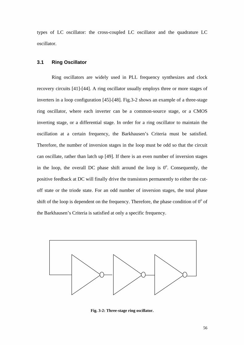
56
types of LC oscillator: the cross-coupled LC oscillator and the quadrature LC
oscillator.
3.1 Ring Oscillator
Ring oscillators are widely used in PLL frequency synthesizes and clock
recovery circuits [41]-[44]. A ring oscillator usually employs three or more stages of
inverters in a loop configuration [45]-[48]. Fig.3-2 shows an example of a three-stage
ring oscillator, where each inverter can be a common-source stage, or a CMOS
inverting stage, or a differential stage. In order for a ring oscillator to maintain the
oscillation at a certain frequency, the Barkhausen’s Criteria must be satisfied.
Therefore, the number of inversion stages in the loop must be odd so that the circuit
can oscillate, rather than latch up [49]. If there is an even number of inversion stages
in the loop, the overall DC phase shift around the loop is 0o. Consequently, the
positive feedback at DC will finally drive the transistors permanently to either the cut-
off state or the triode state. For an odd number of inversion stages, the total phase
shift of the loop is dependent on the frequency. Therefore, the phase condition of 0o of
the Barkhausen’s Criteria is satisfied at only a specific frequency.
Fig. 3-2: Three-stage ring oscillator.

57
The oscillation frequency of a ring oscillator is determined by either the 3-dB
bandwidth of each stage or the time delay of each stage, depending on whether the
circuit is working in a small signal condition with an output resistance or in a large
signal condition with the rail-to-rail swing [49]. Hence, the oscillation frequency of an
N-stage ring oscillator can be tuned by varying the time delay of each stage [46].
In the absence of a frequency selective network, the ring oscillator is easy to
implement with the current integration technology, but it suffers from a relatively
high phase noise level, compared to that of the LC oscillator [45], which will be
discussed in the next section. The switching activities in a ring oscillator introduce a
lot of disturbances in the oscillator. In addition, the multiple-stage design also
increases the noise level, making the ring oscillator unpopular in RF systems. A
general discussion of the ring oscillator phase noise is given in [50] and the resulting
phase noise is given by
202 )()(
ωω
ω∆
⋅⋅=∆A
nk V
kTRAL
where Ak is a factor depending on the noise generation mechanism studied, Rn is an
equivalent noisy resistor, VA is the voltage amplitude of the signal, ω0 is the
oscillation frequency, and ∆ω is the frequency offset. The only way to lower the
phase noise is to lower the equivalent resistance Rn, but this inherently implies larger
power consumption. Typical noise value is –94 dBc/Hz at 1 MHz offset from a 2.2
GHz carrier [50] or –83 dBc/Hz at 100 kHz offset from a 900 MHz carrier [51].
(3.5)

58
3.2 Cross-Coupled LC VCO
Fig. 3-3 shows a parallel LC resonator. The quality factor of a resonator using
an inductor with a series resistor R is given by
CL
RCRLCRL
LR
RLQ
ppp
pp
11=====
ωωωω
where Rp ≈ Q2R [52] is the equivalent parallel resistance of the inductor. The quality
factor can also be defined as [19]
Q = 2π(Peak Energy Stored)/(Energy Loss Per Cycle)
Fig. 3-3: Simplified parallel LC resonator.
For an ideal resonator, the value of R is equal to zero, and Q is infinite. In
other words, the ideal resonator would not need to have active devices and no energy
is needed to maintain the oscillation once the oscillation starts. However, in practice
(3.6)
(3.7)
C
R
L
Z p

59
the Q of an on-chip inductor is quite low, typically from 3 to 20. This is mainly due to
their parasitic series resistance and the substrate loss [12]. An LC Oscillator is usually
implemented in a cross-coupled structure shown in Fig. 3-4, which has differential
outputs. This is an advantage because the most commonly used mixer in RF systems
is the double balanced Gilbert-cell mixer where differential inputs are needed.
Fig. 3-4: The cross-coupled LC VCO.
The operation of the cross-coupled LC VCO can be viewed as two identical
colpitts oscillators in a cross-coupled configuration. Each of them serves the other as
C C
L
Vcont
I tail Vbias
VDD
L
M 1 M 2
X
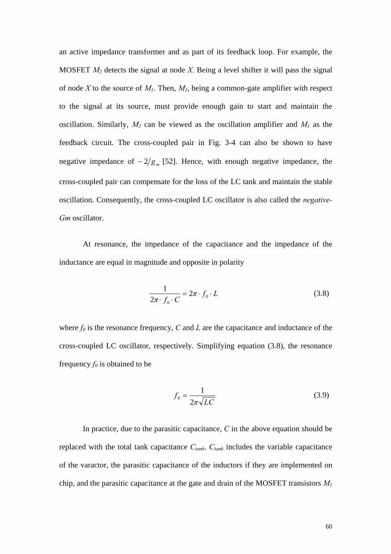
60
an active impedance transformer and as part of its feedback loop. For example, the
MOSFET M2 detects the signal at node X. Being a level shifter it will pass the signal
of node X to the source of M1. Then, M1, being a common-gate amplifier with respect
to the signal at its source, must provide enough gain to start and maintain the
oscillation. Similarly, M2 can be viewed as the oscillation amplifier and M1 as the
feedback circuit. The cross-coupled pair in Fig. 3-4 can also be shown to have
negative impedance of mg2− [52]. Hence, with enough negative impedance, the
cross-coupled pair can compensate for the loss of the LC tank and maintain the stable
oscillation. Consequently, the cross-coupled LC oscillator is also called the negative-
Gm oscillator.
At resonance, the impedance of the capacitance and the impedance of the
inductance are equal in magnitude and opposite in polarity
LfπCfπ
⋅⋅=⋅⋅ 0
0
22
1
where f0 is the resonance frequency, C and L are the capacitance and inductance of the
cross-coupled LC oscillator, respectively. Simplifying equation (3.8), the resonance
frequency f0 is obtained to be
LCπf
21
0 =
In practice, due to the parasitic capacitance, C in the above equation should be
replaced with the total tank capacitance Ctank. Ctank includes the variable capacitance
of the varactor, the parasitic capacitance of the inductors if they are implemented on
chip, and the parasitic capacitance at the gate and drain of the MOSFET transistors M1
(3.8)
(3.9)

61
and M2. Hence, the resonant frequency can be tuned by varying the varactor
capacitance through a control voltage.
3.2.1 Figure of Merit
Compared to Fig. 3-3, where the quality factor of the total parasitic
capacitance QP is not taken into account, a more realistic oscillator’s resonator is
shown in Fig. 3-5. The quality factor of the inductor QL and the quality factor of the
capacitor QC are modeled by series resistance RL = ωL/QL and RC = 1/(QCωC),
respectively. CP describes the loading capacitance due to the total parasitic
capacitance of the cross-coupled transistors and the buffer, and the series resistance is
given by RP = 1/(QPωC). CP is mainly formed by Cgs, Cdb and Cgd of the cross-
coupled transistors and the buffer.
Fig. 3-5: A more realistic model for the resonator tank.
Then, the loaded quality factor Q of this resonator is obtained as
C C P
R C R L
L
R P
62
⎟⎟⎠
⎞⎜⎜⎝
⎛+
++=
P
P
CPL QC
QC
CCQQ111
The Leeson [26] heuristic expression for the phase noise L(∆ω) of an LC VCO
in the 1/f2 region is given by
22
20
2)(
ωω
ω∆
=∆QP
kTFLsig
where Q is the loaded quality factor of the resonator as defined in equation (3.10),
∆ω = 2π∆f is the angular frequency offset, Psig is the average signal power (in watts),
and F is the device noise excess factor. This equation was verified in [86].
The figure of merit (FOM) is commonly used to determine the phase noise
performance of a VCO, with respect to the power and oscillation frequency at a
certain offset frequency [53]
])[(1)( 20
mWLPFOM
vco ωωω
∆∆=
where Pvco is the total power consumption of a VCO in milli-watts. Therefore, from
equations (3.11) and (3.12)
( )212 QkTP
PF
FOMvco
sig ××=
Equation (3.13) shows that the FOM is proportional to the squared quality
factor of the resonator.
In order to compare between VCOs with different Q to reflect a change in
performance that is independent of Q, for example, due to a change in circuit topology,
(3.10)
(3.11)
(3.12)
(3.13)

63
equation (3.13) must be normalized. An arbitrary value of Q = 10 is taken as the
nominal value, the normalized FOM is
210Q
FOMFOMNORM =
In this work, both equation (3.13) and equation (3.14) will be used.
Table 3-1 shows the state-of-the-art LC cross-coupled VCOs, with their
corresponding FOMs.
Table 3-1: Performance comparison of the state-of-the-art cross-coupled LC oscillators.
Ref. 0f (Hz) f∆ (Hz) Phase Noise
@ f∆ (dBc/Hz)
Power (mW)
FOM (dB)
Tuning Range
(%)
[57] 1.80G 3M -130.0 6.0 177.8 4.5
[11] 1.10G 600k -126.0 12.7 180.2 17.0
[58] 1.20G 3M -153.0 9.2 196.0 20.0
[59] 1.80 600k -121.0 6.0 182.7 -
[60] 1.90 100k -100.0 12.0 174.8 14.5
From Table 3-1, it can be seen that [58] has the best FOM. [58] utilized a
filtering technique to lower the LC oscillator’s phase noise. It is reported to be able to
lower the phase noise of differential oscillators to its fundamental minimum permitted
by the resonator quality factor and allocated power consumption. The drawback of
this technique is that the noise filter requires a large inductor of 10nH and a capacitor
of 40pF.
(3.14)
64
In Chapter 5, a novel cross-coupled LC VCO that reduces the intrinsic flicker
noise generation of the tail transistor will be presented. In Chapter 6, a novel VCO for
high frequency application, for example, SONET’s CDR is presented. This VCO is
shown able to operate beyond the transit frequency ft of the transistor used. Notably,
both methods are able to produce a high FOM, without using extra filtering circuitry.
3.3 Quadrature Oscillator
In a transceiver design, quadrature signals are needed for LO inputs of image-
reject mixers, which can achieve a reasonable image rejection without an external RF
filter [62]. The quadrature oscillator is also used in modern transceiver for up and
down conversion of I/Q baseband signals. Most oscillators produce a single-phase
output signal or differential output signals. In order to obtain quadrature signals, a
phase shift network is required. However, an integrated phase shifter suffers from the
amplitude imbalance and phase errors between the quadrature outputs as the oscillator
frequency changes [63]. The quadrature VCO as shown in Fig. 3-6 offers an
alternative solution. It comprises two cross-coupled VCOs as shown in Fig. 3-4 with
additional coupling transistors inserted in parallel with the oscillator. Shown in
Fig. 3-6, the balanced outputs of VCO A are directly coupled to the coupling
transistors in VCO B, and the outputs of VCO B are cross-coupled to the coupling
transistors in VCO A. The two oscillators are forced into quadrature phases by the
coupling topology at the same frequency. The mechanism of the quadrature
generation was explained in [64] and [106].
As shown in Fig. 3-6, the phasors VA and VB are the steady state output
voltages of the two oscillators and are of opposite polarity with -VA and -VB,
respectively. The phasor current I1 is equal to gm(VB - VA), and the phasor current I2 is
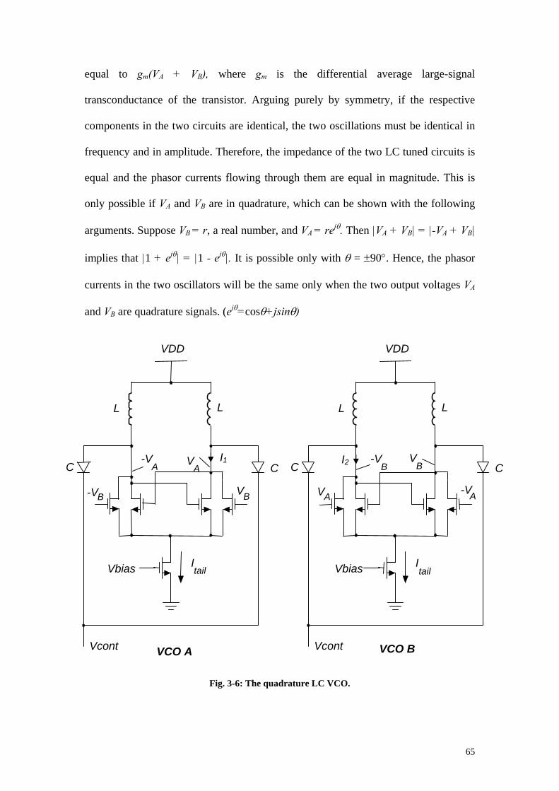
65
equal to gm(VA + VB), where gm is the differential average large-signal
transconductance of the transistor. Arguing purely by symmetry, if the respective
components in the two circuits are identical, the two oscillations must be identical in
frequency and in amplitude. Therefore, the impedance of the two LC tuned circuits is
equal and the phasor currents flowing through them are equal in magnitude. This is
only possible if VA and VB are in quadrature, which can be shown with the following
arguments. Suppose VB = r, a real number, and VA = rejθ. Then |VA + VB| = |-VA + VB|
implies that |1 + ejθ| = |1 - ejθ|. It is possible only with θ = ±90°. Hence, the phasor
currents in the two oscillators will be the same only when the two output voltages VA
and VB are quadrature signals. (ejθ=cosθ+jsinθ)
Fig. 3-6: The quadrature LC VCO.
C C
L
Vcont
I tail Vbias
VDD
L
-V A V
A C C
L
Vcont
I tail Vbias
VDD
L
-VB
V B
-VAVA-V B VB
VCO A VCO B
I1 I2
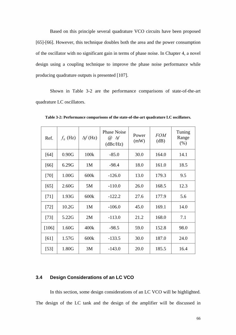
66
Based on this principle several quadrature VCO circuits have been proposed
[65]-[66]. However, this technique doubles both the area and the power consumption
of the oscillator with no significant gain in terms of phase noise. In Chapter 4, a novel
design using a coupling technique to improve the phase noise performance while
producing quadrature outputs is presented [107].
Shown in Table 3-2 are the performance comparisons of state-of-the-art
quadrature LC oscillators.
Table 3-2: Performance comparisons of the state-of-the-art quadrature LC oscillators.
Ref. 0f (Hz) f∆ (Hz) Phase Noise
@ f∆ (dBc/Hz)
Power (mW)
FOM (dB)
Tuning Range
(%)
[64] 0.90G 100k -85.0 30.0 164.0 14.1
[66] 6.29G 1M -98.4 18.0 161.0 18.5
[70] 1.00G 600k -126.0 13.0 179.3 9.5
[65] 2.60G 5M -110.0 26.0 168.5 12.3
[71] 1.93G 600k -122.2 27.6 177.9 5.6
[72] 10.2G 1M -106.0 45.0 169.1 14.0
[73] 5.22G 2M -113.0 21.2 168.0 7.1
[106] 1.60G 400k -98.5 59.0 152.8 98.0
[61] 1.57G 600k -133.5 30.0 187.0 24.0
[53] 1.80G 3M -143.0 20.0 185.5 16.4
3.4 Design Considerations of an LC VCO
In this section, some design considerations of an LC VCO will be highlighted.
The design of the LC tank and the design of the amplifier will be discussed in

67
separated sections. Shown in Fig. 3-7 is a complementary cross-coupled LC VCO.
The inductance is denoted as 2L to reflect the actual implementation of two inductors
with mirror layout strategy for symmetry consideration.
Fig. 3-7: The complementary cross-coupled LC VCO.
3.4.1 Design of the LC Tank
As compared with all the other types of LC VCOs, the cross-coupled LC VCO
suffers from a tradeoff between the phase noise performance and the tuning range at a
given power consumption. From equation (3.9), it can be shown that for a certain
oscillation frequency, the inductance L has to be decreased if the varactor’s
C
VDD
C2L
Vcont
P1 P2
N1 N2
IT

68
capacitance C is increased. In [53], it is said that the power consumption decreases
quadratically with respect to the increment of the tank inductance. Furthermore, in
[54], it is stated that although the inductance L and the series resistance R (refer to
Fig. 3-3) are scaled proportionally, the equivalent parallel resistance Rp still increases
linearly with L. This is because the equivalent parallel resistance of an inductor can be
expressed as Rp ≅ (Lω)2/R. This suggests that the value of the inductance L has to be
maximized for better phase noise performance at a given power consumption.
The power consumption of the resonator in Fig. 3-4 is given by the following
equation [53]
22peakanktpeakloss V
LRCRIP ==
where Vpeak and Ipeak are the peak amplitude voltage across the capacitor and the peak
amplitude current through the inductor respectively. Substituting (3.9) into (3.15)
gives
22
02 peakloss VωLRP =
Fig. 3-8: A simplified physical model of a spiral inductor.
(3.15)
(3.16)
L
C 1 R 1
2
C s
R s
C 1 R 1
1

69
However, in order to know the effect of L on the power consumption, the
relationship between L and R needs to be determined. The assumption made is that ω0
and Vpeak are constant. Fig. 3-8 shows a simplified physical model of a spiral inductor
[55]. Fig. 3.9 (a) is an example illustration of the inductor structure. The two metal
layers used are Top Metal and Metal 4. The width and the spacing of the metal stripe
is denoted as w and s respectively. Fig. 3-9 (b) shows a die photo of a spiral inductor.
(a)
Cross-under
(b)
Fig. 3-9: (a) The structure of a spiral inductor; (b) The die photo of a spiral inductor.
w
Top Metal Metal4
s

70
In Fig. 3-8, L is the inductance, Rs denotes the effective series resistor of the
inductor, i.e. the resistance of the metal line. L and Rs are modeled by the following
equations [56]
αw
/A
/r
L ηηw
AKLr
352
23
=
rAr
metal
metals η
δwwA
tρ
R ⎟⎠⎞
⎜⎝⎛ +=
11
In the equations (3.17) and (3.18), H/me.K L 731 −= , sw
wηw += ,
2
⎟⎟⎠
⎞⎜⎜⎝
⎛=
o
R
metal
metal
ωK
tρ
δ , Hz/Ωm.K R ⋅⋅= 91063 , ηAr is the ratio of the metal area and the
total area, metal
metal
tρ
is the sheet resistance of the metal, Ar is the area of the inductor and
ωo is the operating frequency. This model is accurate for lightly doped substrate as
long as the assumption of a lumped model is valid [55].
The shunt capacitance Cs represents the capacitance that arises from the
overlaps of the cross-under and the main spirals, and is determined by the overlapped
area and the thickness of the oxide between the cross-under and the main spirals. R1
and C1 represent the substrate parasitic resistance and the substrate parasitic
capacitance, respectively. R1 and C1 can be approximated as subwlG
R 21 ≈ and
21subwlC
C ≈ [55], where Gsub and Csub are fitting parameters that are constant for a
given substrate. The typical values of Gsub and Csub are 10-7S/µm2 and 10-3~
10-2fF/µm2, respectively.
(3.17)
(3.18)

71
The plot of the equivalent series resistance R versus the inductance L is shown
in Fig. 3-10. This plot is obtained by varying the number of turns in the inductor while
keeping the diameter of the hollowed center core, metal width and metal spacing
constant. The plot of the quality factor Q versus the inductance L is shown in
Fig. 3-11. As Q = (Lω0)/R, equation (3.16) becomes
2
0
1peakloss V
QLωP =
Fig. 3-10: Plot of the equivalent series resistance R versus the inductance L.
(3.19)

72
Fig. 3-11: Plot of the quality factor Q versus the inductance L.
From Fig. 3-11, the quality factor can be approximated as Q = –kL + Q0,
where –k is the slope of the curve and Q0 is the quality factor when L = 0.
Substituting this equation into equation (3.19) yields
2
00
1peakloss V
)LωQ(-kLP
+=
By taking the derivative of the above equation, the minimum point of Ploss can
be found when L = Q0/(2k). This means that Ploss will increase with an increase in L
after this point, which is undesirable. It can be concluded that L needs to be optimized
in the design. This conclusion is in agreement with the results in [75] and [77]. In
addition, the maximum value of L is limited by the self-resonance frequency of the
inductor [54].
(3.20)
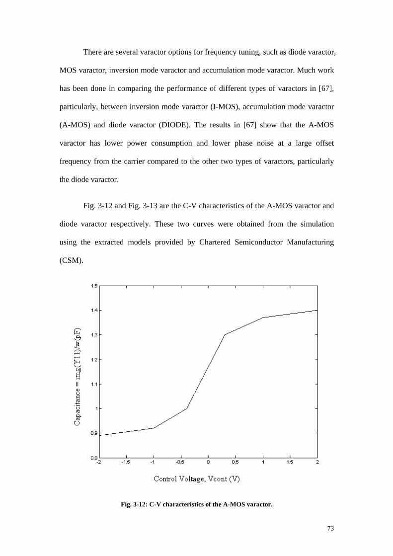
73
There are several varactor options for frequency tuning, such as diode varactor,
MOS varactor, inversion mode varactor and accumulation mode varactor. Much work
has been done in comparing the performance of different types of varactors in [67],
particularly, between inversion mode varactor (I-MOS), accumulation mode varactor
(A-MOS) and diode varactor (DIODE). The results in [67] show that the A-MOS
varactor has lower power consumption and lower phase noise at a large offset
frequency from the carrier compared to the other two types of varactors, particularly
the diode varactor.
Fig. 3-12 and Fig. 3-13 are the C-V characteristics of the A-MOS varactor and
diode varactor respectively. These two curves were obtained from the simulation
using the extracted models provided by Chartered Semiconductor Manufacturing
(CSM).
Fig. 3-12: C-V characteristics of the A-MOS varactor.

74
Fig. 3-13: C-V characteristics of the diode varactor.
From Fig. 3-13, it can be observed that the tuning characteristic of the diode
varactor has a gradual change in slope. From Fig. 3-12, for the A-MOS varactor, the
tuning characteristic is linear in limited region for the control voltage from –0.4V to
0.3V. Fig. 3-12 shows that the slope of the C-V curve is the steepest in the linear
region. Thus, a small change in the control voltage will cause a large deviation of the
capacitance, hence the oscillation frequency. Noise introduced into the control voltage
will result in a large phase noise due to the large Kvco [69]. In [69], an additional term
was added into the Leeson’s formula in equation (2.14) to take into account the noise
generated by the VCO at the varactor terminals that will modulate the carrier and
create additional phase noise. Equation (2.14) is modified to be
])(2
2(
21)
2(1)[1(2)( 20
ωπ
ωω
ωω
ω∆
+∆
+∆
+⋅=∆ mvco
L
c
svco
VKQP
FkTS (3.21)
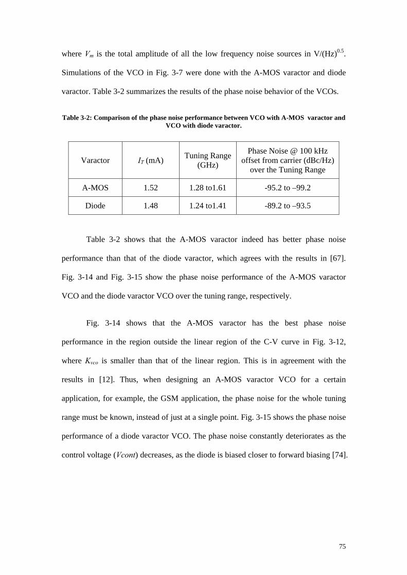
75
where Vm is the total amplitude of all the low frequency noise sources in V/(Hz)0.5.
Simulations of the VCO in Fig. 3-7 were done with the A-MOS varactor and diode
varactor. Table 3-2 summarizes the results of the phase noise behavior of the VCOs.
Table 3-2: Comparison of the phase noise performance between VCO with A-MOS varactor and VCO with diode varactor.
Varactor IT (mA) Tuning Range (GHz)
Phase Noise @ 100 kHz offset from carrier (dBc/Hz)
over the Tuning Range
A-MOS 1.52 1.28 to1.61 -95.2 to –99.2
Diode 1.48 1.24 to1.41 -89.2 to –93.5
Table 3-2 shows that the A-MOS varactor indeed has better phase noise
performance than that of the diode varactor, which agrees with the results in [67].
Fig. 3-14 and Fig. 3-15 show the phase noise performance of the A-MOS varactor
VCO and the diode varactor VCO over the tuning range, respectively.
Fig. 3-14 shows that the A-MOS varactor has the best phase noise
performance in the region outside the linear region of the C-V curve in Fig. 3-12,
where Kvco is smaller than that of the linear region. This is in agreement with the
results in [12]. Thus, when designing an A-MOS varactor VCO for a certain
application, for example, the GSM application, the phase noise for the whole tuning
range must be known, instead of just at a single point. Fig. 3-15 shows the phase noise
performance of a diode varactor VCO. The phase noise constantly deteriorates as the
control voltage (Vcont) decreases, as the diode is biased closer to forward biasing [74].
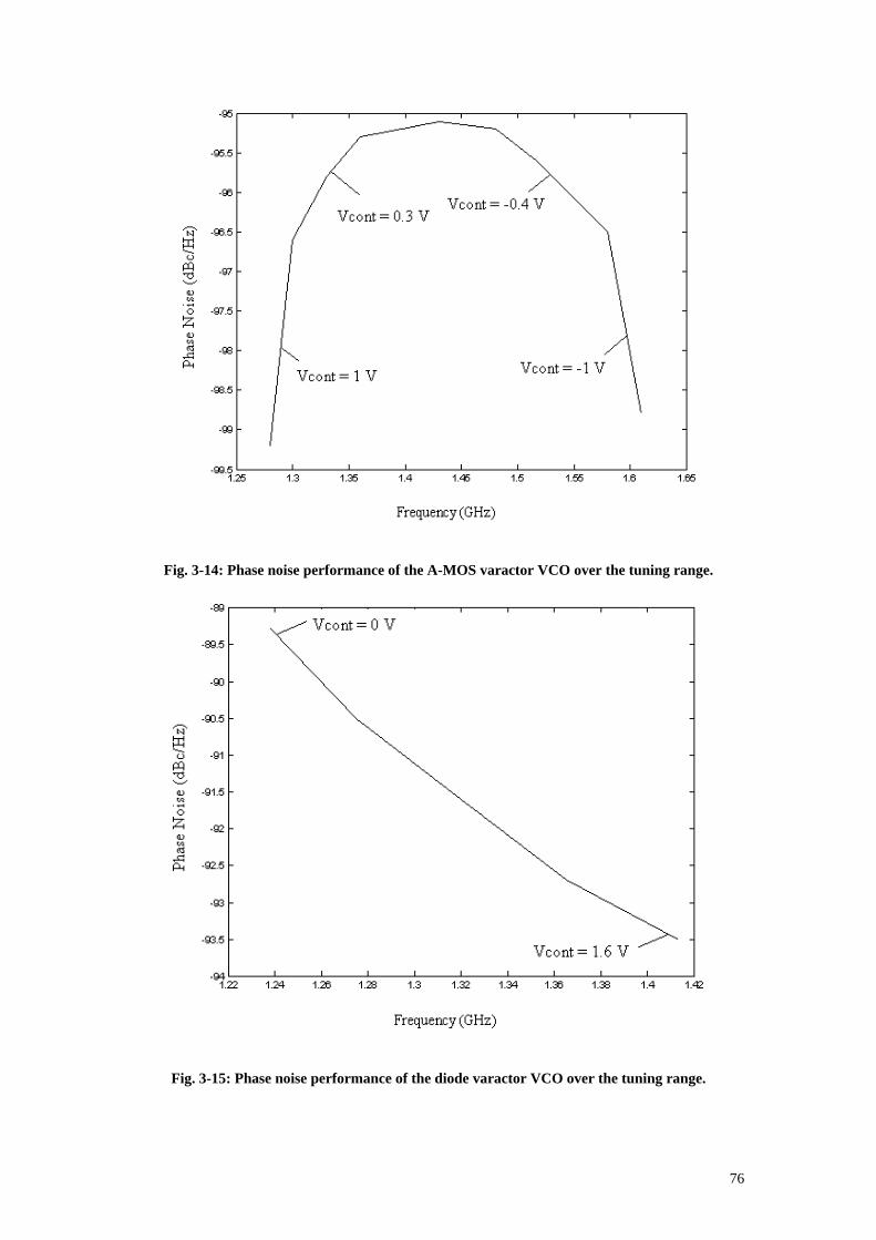
76
Fig. 3-14: Phase noise performance of the A-MOS varactor VCO over the tuning range.
Fig. 3-15: Phase noise performance of the diode varactor VCO over the tuning range.

77
3.4.2 The Design of Amplifier
Fig. 3-16: Tank model of the complementary LC VCO.
The tank model of the complementary LC VCO can be shown as Fig. 3-16
[75]. The load conductance (gtank) is given by
2)/ggg(gg Lvd,pd,nktan +++=
Cdb, p+ Cgs,p Cdb, p+ Cgs,p
-gm,p
4Cgd,p
CL
Rp
RsL
RvCv
4Cgd,n
-gm,n
Cload
Cdb, n+ Cgs,n
-gm,p
4Cgd,p
CL
Rp
Rs
Rv
4Cgd,n
-gm,n
L
Cv
Cload
Cdb, n+ Cgs,n
(3.22)

78
where the effective parallel varactor conductance gv, and the effective parallel
inductor conductance gL, are given by [75]
v
vv Q
ωCg =
LωQ/RL(Rg
TsPL
1)11
2 =+=ω
where QT is the quality factor of the resonator tank and ω is the resonant frequency.
The transconductance of a short channel device can be defined as [79]
50]2[ .dsoxm (W/L)IµCg =
where µ is the mobility of the carriers in the channel, Cox is the oxide capacitance, W
is the transistor width, L is the transistor length, and Ids is the drain-source transistor
current. In order to satisfy the Barkhausen’s Criteria, the following equation must be
satisfied
2)/g(ggα m,pm,nktang +≤
where αg is the small signal gain (or excess gain) of the resonator tank. For a
symmetric tank, gm,n = gm,p, which will improve the 1/f3 corner of the phase noise [59].
αg is typically chosen to be 2 to 3, so that the transconductance of the amplifying
transistors is large enough to ensure the gain of the resonator tank is larger than unity
at the resonant frequency. Thus, the oscillation can be maintained. With noise at other
frequencies being suppressed, the noise component at the resonant frequency is
amplified, passed into the positive feedback loop and further amplified till the
(3.23)
(3.24)
(3.25)
(3.26)

79
transistor enters the saturation region so that the oscillation amplitude is maintained.
Substituting equation (3.25) into equation (3.26) gives
LQIL
W)g/(g dsmg ωα ⋅⋅∝≤ tank1
For low power design, the biasing current Ids must be kept low. In order to
keep the transconductance constant and hence the gain constant in (3.27), larger W/L
for N1, N2, P1 and P2 (in Fig. 3-7) will be required, which increases the parasitic
capacitance to the LC tank. Since the parasitic capacitance cannot be controlled, the
overall controllable capacitance range will be limited and the tuning range of the
VCO will be restricted. Hence, there is a tradeoff between the power consumption and
the frequency range. Therefore, the amplifying transistors must be designed to
provide a good compromise for these two factors.
3.5 Summary
In this chapter, a review of various VCO designs was presented. Some design
considerations, particularly the design of the LC tank and the design of the amplifier,
were discussed. In the next three chapters, three novel implementations of LC VCOs
will be presented.
(3.27)

80
CHAPTER 4
Parasitic-Compensated Quadrature
LC Oscillator
LC voltage-controlled oscillator (VCO) is commonly used as local oscillator
of transceivers. It is a bottleneck in the design of a fully integrated radio frequency
(RF) circuit. Compared to other topologies, such as inverter-based ring oscillator, LC
oscillator is preferred because of its high quality factor (Q). However, the Q value of
an integrated inductor is poor in the CMOS technology due to the high substrate loss,
which generates the thermal noise and causes significant phase noise in the VCO [77].
In order to produce the required quadrature outputs for modern transceivers,
some recent designs [63]-[66] couple two identical differential VCOs. However, this
technique doubles both the area and the power consumption of the oscillator without
any significant gain in terms of phase noise reduction. The design in this chapter aims
to use the coupling technique to improve the phase noise performance while
producing quadrature outputs.
This chapter starts with a brief analysis of the effect of a lossy inductor on the
resonant characteristics of a parallel LC resonator. Then, the parasitic-compensated
circuit topology, which is based on the coupling structure [63]-[66], will be
introduced. This will be followed by the analysis and measured results of a parasitic-
compensated LC oscillator.

81
4.1 Effect of a Lossy Inductor on Phase Noise
Fig. 4-1: Parallel LC resonator.
In order to demonstrate the effect of a lossy inductor on phase noise, the
characteristics of an LC tank need to be described. The discussions will be restricted
to a parallel LC resonator used in the design as shown in Fig. 4-1. The effective
impedance of a parallel resonator (Zp) is:
22 1111 ⎟⎠⎞
⎜⎝⎛ −+⎟
⎠⎞
⎜⎝⎛=⎟⎟
⎠
⎞⎜⎜⎝
⎛⎟⎠⎞
⎜⎝⎛ −+=
ωCωL
LCR
ωCωLj
LCRZp
From the above equation, the maximum impedance value of the parallel
resonator would be |Zpmax| = L/(RC) at the resonant frequency ωp, where ωp =
1/(LC)1/2 for ωL >> R. Fig. 4-2 shows the corresponding resonant characteristics. The
quality factor, which is defined as the sharpness of the impedance magnitude versus
frequency characteristic, can be expressed as follows
Lω||Z
Qp
maxpmaxp =
(4.1)
(4.2)
C
R
L
Z p

82
Fig. 4-2: The resonant characteristic of a parallel LC resonator.
However, due to the parasitic effects, the resonator does not oscillate at the
frequency when |Zp| = |Zpmax|. This consequently lowers the Q value, and causes
degradation in the phase noise performance. The resonant impedance and the resonant
frequency in the above discussions are derived under the assumption that the series
resistance of the inductance is much smaller than its reactance (ωL>>R). However,
the Q value of the CMOS integrated inductor is relatively low, so the above condition
cannot be satisfied. If the series resistance of the inductor is included, the impedance
of the parallel LC tank becomes
( )
⎟⎠⎞
⎜⎝⎛ −+
−=
++
+=
ωCRRωLj
ωLRj
CRL
jCωjLωR
jCωjLωR
Z11
1
1
1
(4.3)
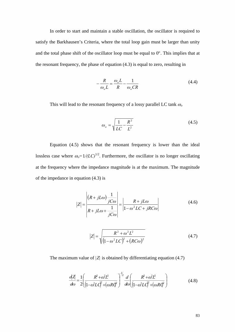
83
In order to start and maintain a stable oscillation, the oscillator is required to
satisfy the Barkhausen’s Criteria, where the total loop gain must be larger than unity
and the total phase shift of the oscillator loop must be equal to 0°. This implies that at
the resonant frequency, the phase of equation (4.3) is equal to zero, resulting in
CRωRLω
LωR
o
o
o
1−=−
This will lead to the resonant frequency of a lossy parallel LC tank ωo
2
21LR
LCωo −=
Equation (4.5) shows that the resonant frequency is lower than the ideal
lossless case where ωo=1/(LC)1/2. Furthermore, the oscillator is no longer oscillating
at the frequency where the impedance magnitude is at the maximum. The magnitude
of the impedance in equation (4.3) is
( )
jRCωLCωjLωR
jCωjLωR
jCωjLωR
Z+−
+=
++
+=
211
1
( ) ( )222
222
1 RCωLCω
LωRZ+−
+=
The maximum value of |Z| is obtained by differentiating equation (4.7)
( ) ( ) ( ) ( ) ⎟⎟⎠
⎞⎜⎜⎝
⎛
+−
+⎟⎟⎠
⎞⎜⎜⎝
⎛
+−
+=
−
222
22221
222
222
1121
ωRCLCωLωR
dωd
ωRCLCωLωR
dωZd
(4.4)
(4.5)
(4.6)
(4.7)
(4.8)
84
When d|Z|/dω = 0, the solution for equation (4.8) will give the frequency at
which the impedance of the lossy parallel LC tank is maximum
LCR
LCR
LCω '
o
22211−+=
Shown in Fig. 4-2, the impedance magnitude peaks at a frequency (ωo’) higher
than the resonant frequency (ωo). Hence, the magnitude of the resonator impedance at
the resonant frequency is lower than its maximum value. Thus, a lower Q value can
be expected, this leads to a degradation of phase noise.
4.2 Parasitic-Compensated LC Oscillator Topology
The parasitic-compensated LC oscillator is based on the coupling structure
[63]-[66], to increase the tuning range [66] and to generate quadrature outputs [64].
However, using the coupling structure to increase the tuning range suffers from the
drawback of the degradation of phase noise as the resonant frequency is shifted
further away from the frequency where the impedance of a LC tank is at maximum.
(4.9)

85
Fig. 4-3: Block diagram of the coupled VCO.
Fig. 4-3 shows the block diagram of the coupled VCO [66]. G1 and G2 are two
identical fixed frequency oscillators. Their outputs are coupled to their inputs with the
coupling coefficients M1 and M2. Both oscillators will synchronize to a single
oscillation frequency ω at the steady state. The outputs of each oscillator must satisfy
the following equations
( ) ( ) XjωGYMX =+ 12
( ) ( ) YjωGXMY =+ 21
where M1 and M2 are scalars, and X and Y are the output phasors for oscillators 1 and
2, respectively. Since the oscillators are identical, G1 = G2 = G and M1 = −M2 = M can
be satisfied. Hence, from equation (4.10) and equation (4.11), it can be shown that
X2 + Y2 = 0 or X = ±jY. Thus, quadrature outputs X and Y are generated [66]. The new
(4.10)
(4.11)
Y G 2
G 1
M 1 M 2
+
+
Vset Vset
X

86
oscillation frequency ω can be found by substituting X = ±jY into equation (4.10) or
equation (4.11)
( ) ( ) 11 =± jωGjM
where ( ) ( ) mGjωZjωG = , and ( )( ) MjωZφ 1tan −±= are the possible conditions for the
oscillation.
The above analysis shows that by selecting a suitable coupling coefficient M,
the resonant frequency can be shifted to the frequency ωo’, where the magnitude of
the impedance is at maximum. The value of M can be controlled by Vset.
(4.12)
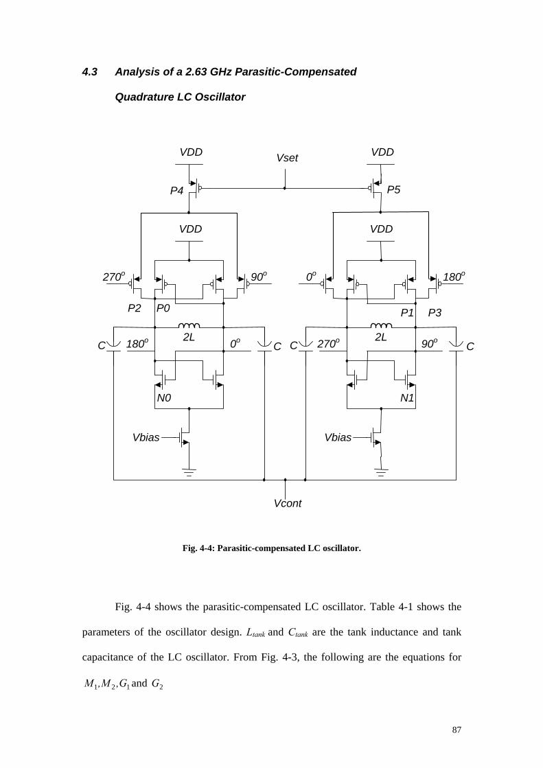
87
4.3 Analysis of a 2.63 GHz Parasitic-Compensated
Quadrature LC Oscillator
Fig. 4-4: Parasitic-compensated LC oscillator.
Fig. 4-4 shows the parasitic-compensated LC oscillator. Table 4-1 shows the
parameters of the oscillator design. Ltank and Ctank are the tank inductance and tank
capacitance of the LC oscillator. From Fig. 4-3, the following are the equations for
121 ,G,MM and 2G
C
VDD
C2L
Vcont
Vbias
VDD
90o 270o
0o 180o
C
VDD
C2L
Vbias
VDD
0o180o
270o 90o
Vset
P2 P0
N0
P1 P3
N1
P4 P5

88
)) 000100
21 (jω)Zg(g(jω;G
gggM PN
PN
P +=+
=
)) 111211
32 (jω)Zg(g(jω;G
ggg
M PNPN
P +=+
=
where gP0, gP1, gP2, gP3, gP4, gP5, gN0 and gN1 are the transconductance of transistors
P0, P1, P2, P4, P5, N0 and N1, respectively. Coupling is achieved through the
coupling coefficients M1 and M2. Equation (4.13) shows that M1 is equal to the
transconductance of transistor P2 divided by the sum of transconductance of
transistors N0 and P0. The transconductance gain of P2 is adjusted by the current
source transistor P4, which is controlled by Vset. From the parameters given in Table
4-1, and by solving equation (4.5), the resonant frequency of a lossy parallel LC tank
ωo is obtained to be 2.59 GHz. Using equation (4.13) and equation (4.14), the
oscillation frequency can be shifted to ωo’= 2.63 GHz with a proper selection of M as
given by equation (4.9), where the maximum impedance is obtained.
Table 4-1: Parameters of the oscillator design.
Tank Inductance, Ltank 1.84nH
Tank Capacitance, Ctank 2.02pF
Series Resistance of Inductor, R 4.30Ω
Using the circuit simulator SpectreRF, the simulated phase noise at the
frequency ωo’ is -112.8 dBc/Hz at 600 kHz offset. The figure was compared with the
phase noise of the same design but without parasitic-compensated circuit. The phase
noise simulations show an improvement of 4dB when parasitic-compensated circuit is
implemented.
(4.13)
(4.14)
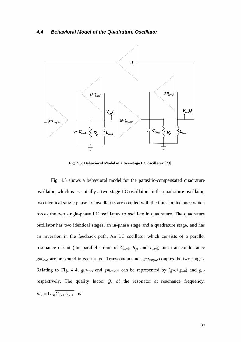
89
4.4 Behavioral Model of the Quadrature Oscillator
Fig. 4.5: Behavioral Model of a two-stage LC oscillator [73].
Fig. 4.5 shows a behavioral model for the parasitic-compensated quadrature
oscillator, which is essentially a two-stage LC oscillator. In the quadrature oscillator,
two identical single phase LC oscillators are coupled with the transconductance which
forces the two single-phase LC oscillators to oscillate in quadrature. The quadrature
oscillator has two identical stages, an in-phase stage and a quadrature stage, and has
an inversion in the feedback path. An LC oscillator which consists of a parallel
resonance circuit (the parallel circuit of Ctank, Rp, and Ltank) and transconductance
gmlevel are presented in each stage. Transconductance gmcouple couples the two stages.
Relating to Fig. 4-4, gmlevel and gmcouple can be represented by (gP0+gN0) and gP2
respectively. The quality factor Qp of the resonator at resonance frequency,
kko LC tantan/1=ω , is
Ctank LtankRP
gmlevel
gmcouple
VoutQ
Ctank LtankRP
gmlevel
gmcouple
VoutI
-1
90
δωδφω
2tan
tan o
k
kpp L
CRQ ==
where δφ/δω is the slope of the phase characteristic of the resonator.
It was shown in [73] that the effective quality factor QN of the N-stage LC
oscillator can be simplified to be
)cos()( respresN QNQ φφ ⋅⋅≈
where N is number of stages of the LC oscillator and φres is the resonator phase
shift. N is 2 in the quadrature oscillator and φres is approximated to be 15°.
As QN ≅ 2Qp, the difference in effective parallel resistance from one frequency
to another frequency is increased, which explains for the large drop in phase noise as
the frequency is moving away from the maximum impedance frequency.
(4.15)
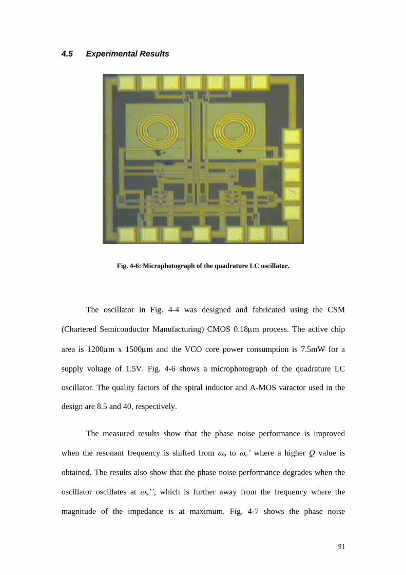
91
4.5 Experimental Results
Fig. 4-6: Microphotograph of the quadrature LC oscillator.
The oscillator in Fig. 4-4 was designed and fabricated using the CSM
(Chartered Semiconductor Manufacturing) CMOS 0.18µm process. The active chip
area is 1200µm x 1500µm and the VCO core power consumption is 7.5mW for a
supply voltage of 1.5V. Fig. 4-6 shows a microphotograph of the quadrature LC
oscillator. The quality factors of the spiral inductor and A-MOS varactor used in the
design are 8.5 and 40, respectively.
The measured results show that the phase noise performance is improved
when the resonant frequency is shifted from ωo to ωo’ where a higher Q value is
obtained. The results also show that the phase noise performance degrades when the
oscillator oscillates at ωo’’, which is further away from the frequency where the
magnitude of the impedance is at maximum. Fig. 4-7 shows the phase noise

92
performance versus Vset. Fig. 4-8 shows the phase noise performance of the oscillator
over the tuning range from 2.59 GHz to 3.13 GHz. Table 4-2 summarizes the
measurement results of the phase noise performance of the VCO. The power spectrum
of the oscillator at ωo’ is shown in Fig. 4-9.
-114
-112
-110
-108
-106
0.00 0.50 1.00 1.50
Vset (V)
Phas
e N
oise
(dB
c/H
z) @
600k
Hz
Fig. 4-7: Phase noise performance versus Vset.
-113
-112
-111
-110
-109
-108
-107
-106
-105
-104
-103
2.59 2.63 2.83 3.03
Frequency (GHz)
Phas
e N
oise
(dB
c/H
z) @
600k
Hz
Fig. 4-8: Phase noise performance over the tuning range from 2.59 GHz to 3.13 GHz.
Vset = 0V
Vset = 1.5V
Vset = 1V

93
Table 4-2: Measurement results of the VCO.
Vset (V) Resonance Frequency
Phase Noise @ 600 kHz offset
0.0 2.59 GHz -108.2 dBc/Hz
1.0 2.63 GHz -112.3 dBc/Hz
1.5 2.65 GHz -109.0 dBc/Hz
Fig. 4-9: Power spectrum of the oscillator at ωo’.
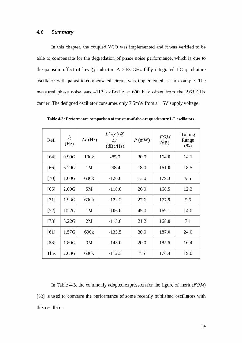
94
4.6 Summary
In this chapter, the coupled VCO was implemented and it was verified to be
able to compensate for the degradation of phase noise performance, which is due to
the parasitic effect of low Q inductor. A 2.63 GHz fully integrated LC quadrature
oscillator with parasitic-compensated circuit was implemented as an example. The
measured phase noise was –112.3 dBc/Hz at 600 kHz offset from the 2.63 GHz
carrier. The designed oscillator consumes only 7.5mW from a 1.5V supply voltage.
Table 4-3: Performance comparison of the state-of-the-art quadrature LC oscillators.
Ref. 0f (Hz)
f∆ (Hz) L( f∆ ) @
f∆ (dBc/Hz)
P (mW) FOM (dB)
Tuning Range
(%)
[64] 0.90G 100k -85.0 30.0 164.0 14.1
[66] 6.29G 1M -98.4 18.0 161.0 18.5
[70] 1.00G 600k -126.0 13.0 179.3 9.5
[65] 2.60G 5M -110.0 26.0 168.5 12.3
[71] 1.93G 600k -122.2 27.6 177.9 5.6
[72] 10.2G 1M -106.0 45.0 169.1 14.0
[73] 5.22G 2M -113.0 21.2 168.0 7.1
[61] 1.57G 600k -133.5 30.0 187.0 24.0
[53] 1.80G 3M -143.0 20.0 185.5 16.4
This 2.63G 600k -112.3 7.5 176.4 19.0
In Table 4-3, the commonly adopted expression for the figure of merit (FOM)
[53] is used to compare the performance of some recently published oscillators with
this oscillator
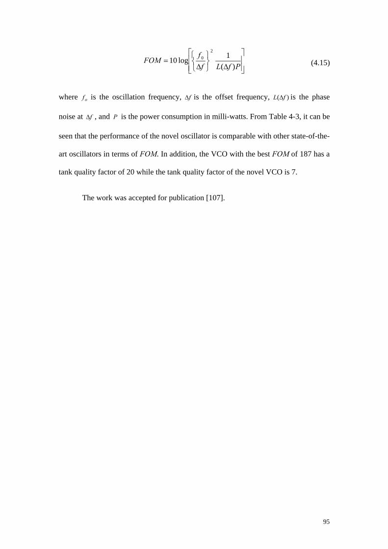
95
⎥⎥⎦
⎤
⎢⎢⎣
⎡
∆⎭⎬⎫
⎩⎨⎧
∆=
PfLff
FOM)(
1log102
0
where of is the oscillation frequency, f∆ is the offset frequency, )( fL ∆ is the phase
noise at f∆ , and P is the power consumption in milli-watts. From Table 4-3, it can be
seen that the performance of the novel oscillator is comparable with other state-of-the-
art oscillators in terms of FOM. In addition, the VCO with the best FOM of 187 has a
tank quality factor of 20 while the tank quality factor of the novel VCO is 7.
The work was accepted for publication [107].
(4.15)
96
CHAPTER 5
RF CMOS Low-Phase-Noise LC Oscillator
Through Memory Reduction Tail Transistor
The challenge in the design of a fully integrated CMOS LC voltage-controlled
oscillator (VCO) is to achieve low phase noise while maintaining low power
consumption. However, the integrated inductor usually has a poor quality factor and
this greatly affects the phase noise performance. While efforts have been made to
improve the phase noise performance by increasing the quality factor of the LC tank
through the implementation of the bond-wire [78],[10] or a special layout technique
[61], others have sought to improve the phase noise performance through improving
the LC VCO circuit topology [12],[79]. Despite these endeavors, the design and
optimization of integrated LC VCOs still pose many challenges to circuit designers as
far as practicality and cost are concerned.
Recently, it was recognized [59],[80] that the tail transistor might be the
largest contributor to the phase noise in a VCO, especially to the 1 / f 3 - shaped phase
noise close to the oscillation frequency [30]. The noise sources from the tail transistor
can be categorized into the high frequency noise source and the low frequency noise
source. The high frequency up-converted flicker noise source of the tail transistor at
twice the oscillation frequency is down-converted into phase noise by a hard
switching oscillator. On the other hand, the low-frequency flicker noise source of the
tail transistor contributes to the phase noise through various mechanisms, such as
AM-to-PM conversion due to the nonlinearity of the varactor, modulation of the bias
point [81], and modulation of tail capacitance [59].

97
In this chapter, a CMOS LC VCO using a new tail transistor topology to
reduce the intrinsic flicker noise is introduced. Section 5.1 and Section 5.2 discuss the
topology of the novel VCO, and the comparison between the novel VCO and the
VCO with a fixed biasing tail transistor (FB) as well as the VCO without tail
transistor (WT). The last section concludes the chapter with an example of a VCO
that meets the system specifications of the WCDMA/CDMA2000.
5.1 VCO Topologies
In this section, three VCO topologies, namely, VCO without a tail transistor,
VCO with a fixed biasing tail transistor and VCO with memory reduced tail transistor
(novel topology) will be discussed.
5.1.1 Without Tail Transistor (WT) Topology
The operation of the VCO with WT topology shown in Fig. 5-1 is as follows.
When the oscillation condition is satisfied, oscillation starts to develop. As the
oscillation amplitude grows larger, it will reach a point where the negative resistance
is not enough to support the positive resistance of the LC tank if the supply voltage
and ground do not first clip the maximum swing. This is where the amplitude stops
growing and a stable oscillation is reached.

98
Fig. 5-1: VCO with without tail transistor topology.
5.1.2 Fixed Biasing (FB) Tail Transistor Topology
Fig. 5-2 shows a VCO with FB topology. The tail transistor is designed to
operate in the saturation region as a current source. Consequently, the tail current
determines the oscillation amplitude. At the resonance frequency, the admittance of L
and C cancel, leaving REQ, the equivalent parallel resistance of the LC tank
ωQLREQ =
The differential voltage swing across the tank is given in first approximation
by
EQtail RIV =tank
C
V D D
C2 L
A
V co n t
(5.1)
(5.2)
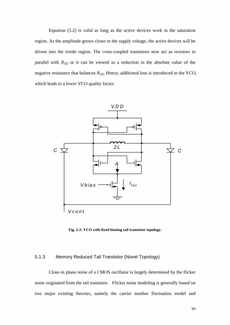
99
Equation (5.2) is valid as long as the active devices work in the saturation
region. As the amplitude grows closer to the supply voltage, the active devices will be
driven into the triode region. The cross-coupled transistors now act as resistors in
parallel with REQ or it can be viewed as a reduction in the absolute value of the
negative resistance that balances REQ. Hence, additional loss is introduced to the VCO,
which leads to a lower VCO quality factor.
Fig. 5-2: VCO with fixed biasing tail transistor topology.
5.1.3 Memory Reduced Tail Transistor (Novel Topology)
Close-in phase noise of a CMOS oscillator is largely determined by the flicker
noise originated from the tail transistor. Flicker noise modeling is generally based on
two major existing theories, namely the carrier number fluctuation model and
C
V D D
C2 L
A
V c o n t
I ta ilV b ia s

100
mobility fluctuation model [82]. The carrier-density fluctuation model predicts an
input referred noise density, which is independent of the gate biasing voltage and is
proportional to the square of oxide thickness. While the mobility fluctuation model
predicts an input referred noise voltage increasing with gate biasing voltage and
proportional to oxide thickness. An often-used model as the basis for circuit
simulations is the unified model [13],[83] with a functional form resembling the
carrier-density fluctuation model at the low bias and the mobility fluctuation model at
the high bias.
The flicker noise is known for its long correlation time and an associated
physical process, which has a “long-term memory” [84]-[85]. The “carrier trapping in
localized oxide states” is a process that plays a significant role in the generation of the
flicker noise in a MOSFET. Moreover, the memory involved with the flicker noise is
related to the long occupation time constants of the traps. As a switched transistor will
force a trap to release its captured electron, rendering the transistor to be memory-less,
the flicker noise is reduced.
Fig. 5-3 shows the simulation setup to investigate the influence of the gate
source voltage switching on the baseband power spectral density of the VCO tail
transistor’s flicker noise current. For comparison, the gates of the two transistors are
driven by a fixed biasing voltage and then by a switched biasing voltage from rail to
rail at 2 GHz. As the supply current for both topologies are made the same, the
difference in the phase noise at point A is mainly due to the VCO’s topology. The
results are shown in Fig. 5-4. The amount of phase noise reduction using switched
biasing compared to fixed biasing is about 8dB at 1 kHz and 5dB at 100 kHz, which
agrees well with the measured results in [84]-[85].

101
Fig. 5-3: Test setup for flicker noise.
D iffe re n tia lIn p u t
V D D
2 L
V G S _ O N
V G S _ O F FV G S
-
+
C C
A
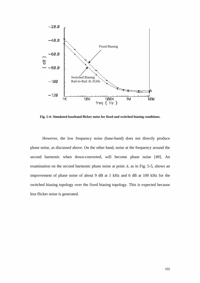
102
Fig. 5-4: Simulated baseband flicker noise for fixed and switched biasing conditions.
However, the low frequency noise (base-band) does not directly produce
phase noise, as discussed above. On the other hand, noise at the frequency around the
second harmonic when down-converted, will become phase noise [49]. An
examination on the second harmonic phase noise at point A, as in Fig. 5-5, shows an
improvement of phase noise of about 9 dB at 1 kHz and 6 dB at 100 kHz for the
switched biasing topology over the fixed biasing topology. This is expected because
less flicker noise is generated.
Fixed Biasing
Switched Biasing Rail-to-Rail At 2GHz

103
Fig. 5-5: Simulated second harmonic flicker noise for fixed and switched biasing conditions.
Fig. 5-6 shows the memory reduced tail transistor VCO. The operation of the
novel oscillator is as follows. Initially, when the circuit is balanced, both the output
voltages and currents flowing in the two sides are set by the size of the tail transistors.
The tail transistors will go into the saturation region first while the cross-coupled
nMOS transistors are still in the cut-off region. When both the tail transistors and
cross-coupled nMOS transistors are in the triode region, the tail transistors determine
the current as the voltages at the source of the cross-coupled nMOS transistors are
floating.
Switched Biasing Rail-to-Rail At 2GHz
Fixed Biasing

104
Fig. 5-6: Memory reduced tail transistor VCO.
Since all the transistors in this VCO topology are switched biasing rather than
fixed biasing, it is expected to have lower flicker noise [84]-[85]. Moreover, as the
transistors operate in the triode region for a large portion of the oscillation period,
they exhibit lower current flicker noise than the transistors that operate in the
saturation region, for example the tail transistor in the FB topology [83].
5.2 Performance Comparisons of the Three VCO Topologies
A comparison of the two conventional topologies with this novel topology will
reveal the advantages and disadvantages of these VCOs.
C
VDD
C2L
A
Vcont

105
The main advantage of the novel topology and WT topology over the FB
topology is that without the tail transistor flicker noise source, the only flicker noise
source now is the cross-coupled transistors, which have an inherently lower flicker
noise due to the switched biasing, resulting in better phase noise performance [84]-
[85].
Another disadvantage of the FB topology compared to the novel topology and
WT topology is that the tail transistor in the FB topology reduces the headroom
available for oscillation by around 0.2 to 0.4 volt in the CMOS 0.25µm technology.
The effect is not negligible for low voltage design. A smaller signal power Psig has an
adverse effect on the phase noise, as phase noise is essentially the noise to signal ratio
of the VCO. The tail transistors of the novel topology mostly work in the triode region,
so the headroom requirement is negligible. The WT topology can achieve the largest
oscillation amplitude among the three topologies.
For the FB topology, extra circuitry is needed to provide biasing voltage to the
tail transistor. This not only increases the power consumption, but also introduces
noise sources to the VCO. The noise current coming from the biasing network will be
mirrored into the tail transistor. Both the novel topology and the WT topology do not
encounter this problem.
The major obstacle in implementing the WT topology is the power
consumption. This is especially true in the case of an over-designed loop gain. For the
complementary LC oscillator, in order to maintain the oscillation, the loop gain
condition is
)R()gg( EQgmpmn 1α>+ (5.3)

106
where αg is the excess gain factor and typically from 2 to 3. gmn and gmp are the
transconductance of the nMOS and pMOS cross-coupled transistors, respectively. The
excess gain factor is a safety margin to guarantee oscillation. However, in the case of
the WT topology, the VCO will consume a lot of “short-circuit current” that is useless
to the functioning of the oscillator. For the same tank characteristics, which include
the excess gain factor αg and the oscillation frequency, the WT topology has the
highest power consumption while both the FB topology and the novel topology have
the same power consumption.
Another disadvantage of the WT topology is the absence of the high tail
transistor impedance in series with the cross-coupled transistors to stop the transistors
from loading the resonator in the triode region [58]. In a balanced circuit, the odd
harmonics circulate in a differential path, while even harmonics flow in a common-
mode path. The even harmonics that are usually dominated by the second harmonic
components travel through the resonator capacitors and the cross-coupled transistors
to ground. The high impedance acts to suppress the noise in the tail transistor by
making it appear noiseless to the VCO, thus improving the phase noise performance.
Compared to the WT topology, the FB topology and the novel topology suppress the
second harmonic noise more and prevent the cross-coupled transistors from loading
the resonator. Thus, an improvement of phase noise in the 1 / f 3 region is expected
from the novel topology and the FB topology over the WT topology. However, the
improvement on the phase noise performance of the VCO with the FB topology is
masked by the up-converted flicker noise of the tail transistor.

107
Finally, the FB topology is less susceptible to the frequency pushing effect,
which is the frequency sensitivity to the voltage supply. Both the WT topology and
the novel topology are affected by the frequency pushing effect.
For comparison, three VCOs with the same tank characteristics and oscillation
frequency are designed and simulated using the three topologies. The excess gain
factor αg is made to be 2.5 and the tank quality factor is about 9.
The oscillators are designed for GSM-1800 applications where the oscillation
frequency is at 1.88 GHz and they are optimized for FOM. All the simulation models
are extracted models from the 0.25µm IBM SiGe 6HP process. However, only CMOS
transistors are used in the simulation. The post-layout simulation performance of the
VCOs for three topologies is summarized in Table 5-1.
Table 5-1: Summary of the performance of the three VCOs.
Without Tail
Transistor Topology (WT)
Fixed Biasing Tail Transistor Topology (FB)
Memory Reduced Tail Transistor
Topology (novel)
Power Consumption
1.7mA * 2V = 3.5 mW
1.4mA * 2V = 2.8mW
1.4mA * 2V = 2.8mW
Phase Noise
-84 dBc/Hz @10 kHz Offset -126.6 dBc/Hz
@600 kHz Offset
-81 dBc/Hz @10 kHz Offset
-126 dBc/Hz @600 kHz Offset
-87 dBc/Hz @10 kHz Offset -127.6 dBc/Hz
@600 kHz Offset
FOM @600 kHz Offset 191.3dB 191.5dB 193dB
Fig. 5-7 shows the phase noise performances of the three VCOs, the stringent
GSM specifications are given as circles in the figure. From Table 5-1, it can be seen
that the novel topology gives the maximum improvement of the phase noise of 6dB

108
from the FB topology and 3dB from the WT topology while consuming lower power
consumption than the WT topology. The novel topology also shows the best FOM of
193dB, which corresponds to a normalized FOM of 194dB using equation (3.14).
Fig. 5-7: Comparison of phase noise performance for the three VCOs.
Evidently, the advantages of the novel topology are that it has a superior phase
noise performance to that of the FB topology while it has lower power consumption
than the WT topology, which gives this novel topology an edge over the other two
topologies.
5.3 Summary
To date, few VCOs have met the specifications of the WCDMA and
CDMA2000 standards due to the stringent phase noise requirement. This is especially
true for fully integrated VCOs due to low Q inductor. Using the novel topology, a
The FB Topology
The WT Topology
The Novel Topology
Stringent GSM Standards: 125 dBc/Hz@600 kHz
Stringent GSM Standards: 112 dBc/Hz@100 kHz

109
VCO optimized for phase noise performance was designed. The specifications of the
VCO are shown in Table 5-2.
Table 5-2: Specifications of the VCO.
Tuning range 2.05 GHz to 2.25 GHz
Excess gain factor, gα 2.5
Estimated tank quality factor 12
Phase Noise @ 600 kHz from 2.05 GHz to 2.25 GHz -129.2 dBc/Hz to –129.3 dBc/Hz
Phase noise @ 8 MHz from 2.05 GHz to 2.25 GHz -152 dBc/Hz to –152.5 dBc/Hz
Power consumption 4.2mA*2V = 8.4mW
Fig. 5-8 shows the phase noise performance of the VCO, and the
WCDMA/CDMA2000 specifications are given as circles. It is shown that the VCO
has exceeded the standard specifications with a low power consumption of 8.4mW.
The FOM for this VCO at 600 kHz offset is 191.5 dB. As a conclusion, the
performance of the novel VCO and other state-of-the-art designs are compared in
Table 5-3.
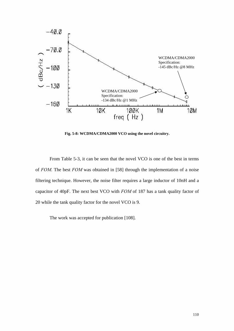
110
Fig. 5-8: WCDMA/CDMA2000 VCO using the novel circuitry.
From Table 5-3, it can be seen that the novel VCO is one of the best in terms
of FOM. The best FOM was obtained in [58] through the implementation of a noise
filtering technique. However, the noise filter requires a large inductor of 10nH and a
capacitor of 40pF. The next best VCO with FOM of 187 has a tank quality factor of
20 while the tank quality factor for the novel VCO is 9.
The work was accepted for publication [108].
WCDMA/CDMA2000 Specification: -145 dBc/Hz @8 MHz
WCDMA/CDMA2000 Specification: -134 dBc/Hz @1 MHz
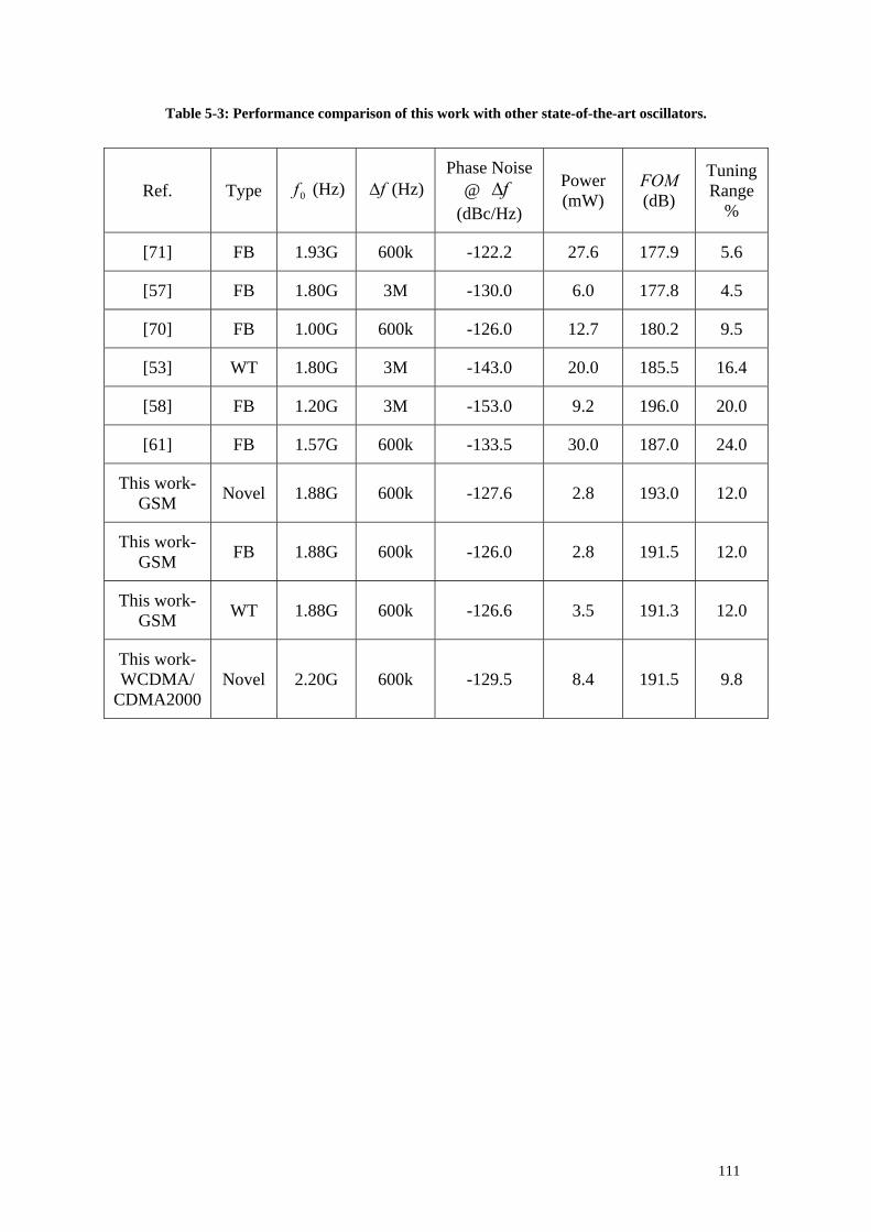
111
Table 5-3: Performance comparison of this work with other state-of-the-art oscillators.
Ref. Type 0f (Hz) f∆ (Hz) Phase Noise
@ f∆ (dBc/Hz)
Power (mW)
FOM (dB)
Tuning Range
%
[71] FB 1.93G 600k -122.2 27.6 177.9 5.6
[57] FB 1.80G 3M -130.0 6.0 177.8 4.5
[70] FB 1.00G 600k -126.0 12.7 180.2 9.5
[53] WT 1.80G 3M -143.0 20.0 185.5 16.4
[58] FB 1.20G 3M -153.0 9.2 196.0 20.0
[61] FB 1.57G 600k -133.5 30.0 187.0 24.0
This work-GSM Novel 1.88G 600k -127.6 2.8 193.0 12.0
This work-GSM FB 1.88G 600k -126.0 2.8 191.5 12.0
This work-GSM WT 1.88G 600k -126.6 3.5 191.3 12.0
This work-WCDMA/
CDMA2000 Novel 2.20G 600k -129.5 8.4 191.5 9.8
112
CHAPTER 6
102 GHz SiGe MOSFETs LC Oscillator
The proliferation of fiber optic communication applications, for example OC-
768 [2], which operates at 40 GHz, has led to a new challenge to the design of a fully
integrated circuit. A good way to compare the performance of different semiconductor
technologies is through tf , which is defined as the frequency where the transistor
current gain becomes unity. To date, the most advanced SiGe technology can achieve
an tf of about 100 GHz. On the other hand, Indium Phosphide (InP) technology can
reach up to 160 GHz. In addition, InP devices will soon reach an tf beyond 200 GHz,
while this seems practically unachievable for SiGe technology due to the very low
break-down voltage. The next generation of optical network that will eventually
replace OC-768 will operate at a frequency beyond 100 GHz.
VCO is an essential component in both multiplexer and demultiplexer for fiber
optical communication applications. In this chapter, a millimeter wave CMOS LC
VCO implementing a push-pull buffer that can double the input frequency was
introduced. The oscillation frequency of the VCO is 102 GHz, which is about twice
the tf of the SiGe CMOS transistors of 52 GHz. Thus, fully integrated VCO using
SiGe can now be realized for applications beyond 100 GHz. The design of high
frequency VCO, layout considerations and the post-layout simulations will be
discussed. The chapter will be concluded with the performance comparison of the
novel VCO with other state-of-the-art high frequency VCOs.
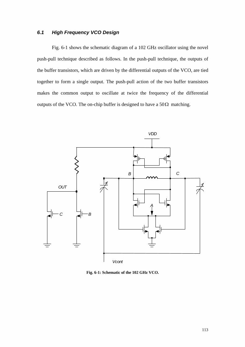
113
6.1 High Frequency VCO Design
Fig. 6-1 shows the schematic diagram of a 102 GHz oscillator using the novel
push-pull technique described as follows. In the push-pull technique, the outputs of
the buffer transistors, which are driven by the differential outputs of the VCO, are tied
together to form a single output. The push-pull action of the two buffer transistors
makes the common output to oscillate at twice the frequency of the differential
outputs of the VCO. The on-chip buffer is designed to have a 50 Ω matching.
Fig. 6-1: Schematic of the 102 GHz VCO.
VDD
A
Vcont
B C
BC
OUT
114
The complementary VCO structure is chosen instead of the nMOS-only
structure as being used in the other two millimeter wave MOSFET VCOs [88], [90],
because of the three disadvantages of the nMOS-only structure [53]. Firstly, for the
nMOS-only structure, the varactor can only be biased with a voltage value larger than
the supply voltage. While the varactor for the complementary structure can be biased
with a voltage value larger than half of the supply voltage. Secondly, to achieve the
same oscillation amplitude, the current must be doubled for the nMOS-only structure
compared to the complementary structure. Thirdly, the output voltage of the nMOS-
only structure is higher than the supply voltage for half the oscillation period, since
the output dc biasing point is at the supply voltage, which limits the long-term
reliability of the circuit.
The post-layout simulation phase noise performance is shown in Fig. 6-2. The
phase noise at B and C is –112 dBc/Hz at 1 MHz offset frequency for the oscillation
frequency of 51 GHz. After the buffer, the frequency is doubled, the oscillation
frequency at OUT is 102 GHz. However, the phase noise deteriorated by 6 dB to –106
dBc/Hz at 1 MHz offset frequency. The reason is that the buffer actually acts as a
frequency multiplier, as the frequency is multiplied by a factor of N, the sideband
noise and spurious response are increased by the multiplication factor. Thus, the phase
noise deteriorates by 20logN [120]. In this case N = 2, as 20log2 ≅ 6 dB, this agrees
with the simulated phase noise drop of 6 dB. The power consumption of the oscillator
and the buffer is 21.4mW at a supply voltage of 2V.
Fig. 6-3 shows the frequency spectrums of the harmonic components of the
102 GHz VCO. The unwanted residual frequency components lie as much as 38.5 dB
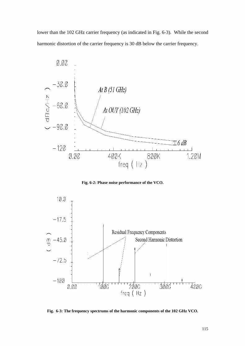
115
lower than the 102 GHz carrier frequency (as indicated in Fig. 6-3). While the second
harmonic distortion of the carrier frequency is 30 dB below the carrier frequency.
Fig. 6-2: Phase noise performance of the VCO.
Fig. 6-3: The frequency spectrums of the harmonic components of the 102 GHz VCO.

116
The main drawback of this structure is the relatively low output swing. At any
one time, one of the buffer transistors will be in the triode region. Hence, a low output
swing is expected, which is obtained to be 210mV. One possible solution to the low
output swing is to add an additional amplification stage after the buffer.
The transistors are optimized for tf , through the selection of the proper
number of fingers, the channel width per finger and the channel length. The S-
parameter post layout simulation results of an nMOS transistor in Fig. 6-4 show that
tf = 52 GHz, and the extrapolated maxf = 98 GHz for =−= TGSeff VVV 0.2V.
Fig. 6-4: ft and fmax plot for Veff = VGS-VT =0.2 V.
The equation for ft is
gdgs
mt CC
gf+
=π2 (6.1)
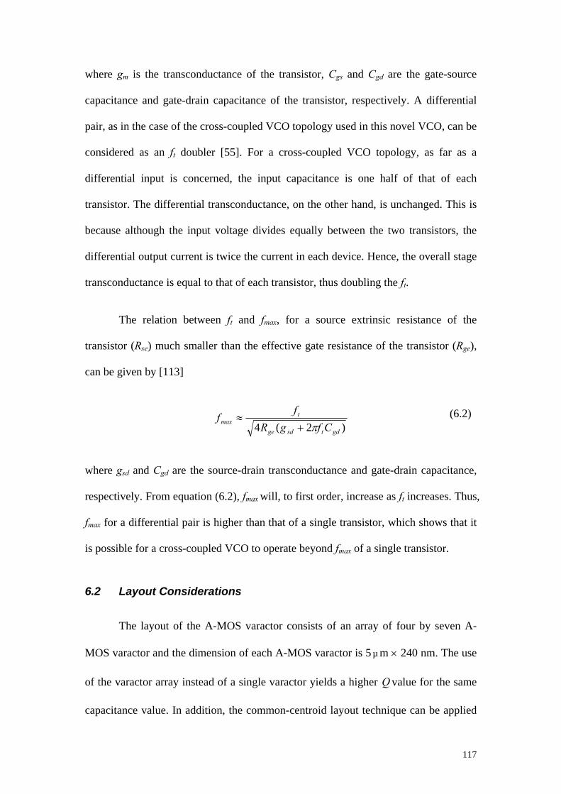
117
where gm is the transconductance of the transistor, Cgs and Cgd are the gate-source
capacitance and gate-drain capacitance of the transistor, respectively. A differential
pair, as in the case of the cross-coupled VCO topology used in this novel VCO, can be
considered as an ft doubler [55]. For a cross-coupled VCO topology, as far as a
differential input is concerned, the input capacitance is one half of that of each
transistor. The differential transconductance, on the other hand, is unchanged. This is
because although the input voltage divides equally between the two transistors, the
differential output current is twice the current in each device. Hence, the overall stage
transconductance is equal to that of each transistor, thus doubling the ft.
The relation between ft and fmax, for a source extrinsic resistance of the
transistor (Rse) much smaller than the effective gate resistance of the transistor (Rge),
can be given by [113]
)2(4 gdtsdge
tmax CfgR
ff
π+≈
where gsd and Cgd are the source-drain transconductance and gate-drain capacitance,
respectively. From equation (6.2), fmax will, to first order, increase as ft increases. Thus,
fmax for a differential pair is higher than that of a single transistor, which shows that it
is possible for a cross-coupled VCO to operate beyond fmax of a single transistor.
6.2 Layout Considerations
The layout of the A-MOS varactor consists of an array of four by seven A-
MOS varactor and the dimension of each A-MOS varactor is 5 µ m × 240 nm. The use
of the varactor array instead of a single varactor yields a higher Q value for the same
capacitance value. In addition, the common-centroid layout technique can be applied
(6.2)

118
to increase the symmetry of the VCO design. Fig. 6-5 shows the frequency response
of the Q and capacitance of the A-MOS varactor. At 51 GHz, the Q and capacitance
of the A-MOS varactor are 66.38 and 132.8fF respectively for the gate to source-drain
voltage of 1V.
Fig. 6-5: Frequency response of the A-MOS varactor.
Stripline inductor is used in the design as it has a remarkable high Q at very
high frequency. Another advantage is its inherently small inductance value, which is
suitable for high frequency design. Three 25 µ m × 100 µ m stripline inductors are used
in parallel to optimize the inductance value, in order to achieve the desired frequency.
Fig. 6-6 shows the frequency response of the Q and inductance of the stripline
inductor. At 51 GHz, the Q and inductance of the stripline inductor are 24.12 and
19.77pH respectively.

119
Fig. 6-6: Frequency response of the stripline inductor.
6.3 Post-Layout Simulation Results
Fig. 6-7: Layout of the 102 GHz VCO.

120
Fig. 6-7 shows the layout of the 102 GHz VCO. The entire chip dimension is
700 µ m × 810 µ m. Table 6-1 shows the results of the post-layout simulation. gα is the
excess gain factor, typically from 2 to 3. For complementary LC oscillator, in order to
maintain the oscillation, the loop gain condition is
)1()( EQgmpmn Rgg α>+
where mng and mpg are the transconductance of the nMOS and pMOS cross-coupled
transistors, respectively.
Table 6-1: Specifications of the 102 GHz VCO.
IBM6HP Process
FOM at offset of 1 MHz 192.9dB
Phase Noise at offset of 1 MHz -106 dBc/Hz to –107.7 dBc/Hz for 98.6 GHz to 102 GHz
Power Consumption VCO Core: 4.5mA*2V = 9mW Buffer: 6.2mA*2V = 12.4mW
Tuning range for control voltage, Vcont from 0.4V to 2.0V
98.6 GHz to 102 GHz (3.4 GHz)
Tank Quality Factor, Q 17
Oscillation Amplitude before buffer (B and C) 1.85 Vpp
Oscillation Amplitude (OUT) 0.21 Vpp
Excess gain factor, gα 2.5
(6.3)

121
6.4 Summary
Table 6-2 shows the performance comparisons of the novel VCO with other
state-of-the-art high frequency VCOs. From Table 6-2, it can be seen that apart from
the very high frequency that has been obtained, the performance of the novel VCO
exceeds the next best VCO by 10.1 dB in terms of FOM.
Table 6-2: Performance comparison of the very high frequency VCOs.
Ref. 0f (GHz)
f∆ (Hz)
Phase Noise (dBc/Hz)
Power (mW) FOM ( dB )
Tuning Range %
[88] 50.0 1M -100.0 13.0 182.8 2.2
[89] 47.3 1M -108.5 280.0 177.5 8.5
[90] 51.6 1M -85.0 1.0 179.3 2.8
This-102 102.0 1M -106.0 21.4 192.9 3.4

122
CHAPTER 7
Frequency Divider
The most apparent feature that differentiates a phase-locked loop (PLL)
synthesizer from other phase-locked loops lies in the frequency divider. Much
attention and efforts have been given to this circuit block to minimize its power
consumption and size and to improve its speed [96]-[99].
This chapter will begin with the discussion on various types of frequency
dividers. The mechanism together with the limitations and advantages of these
frequency dividers will be the focus in the discussion. Subsequently, the design of
several high-speed flip-flops will be compared. Finally, various spur reduction
techniques will be reviewed.
7.1 Types of Frequency Dividers
In this section, a number of divider topologies will be described, namely,
integer-N divider, prescaler, dual-modulus prescaler with swallow counter, and
fractional-N divider.
7.1.1 Integer-N Divider
A popular implementation of an integer-N divider is through a presettable
divider. The presettable divider is used to obtain a variable, controllable division ratio
[29]. A typical element of the divider is the J-K flip-flop with the asynchronous set (S)
and reset (R) capability.

123
A certain preset number can be loaded into the counter, which starts counting
input pulses till the end number is reached and an overflow signal is generated. The
counter is then reset to the original preset number and starts counting again. The
division ratio is equal to (2n – P), where n is the number of bits of the counter and P is
the preset number. An alternative implementation is to start counting input clock
pulses from zero, till a certain preset number P is reached and a reset signal is
generated. Then the counter is reset to zero and the counting process restarts. The
division ratio then equals P. The limitation of the presettable divider is its low
operating frequency.
7.1.2 Prescaler
When the input frequency of the divider is too high to permit a proper
operation of the programmable divider or counter, a prescaler can be used. A
prescaler divides the input frequency by fixed ratios, and can therefore operate at
higher frequencies because it does not suffer from the delays involved in counting and
resetting [29]. Adding a few high-speed prescaler stages will lower the speed
requirement for the subsequent counter stages.
The disadvantage of using the prescaler is that it requires a low reference
frequency for a given frequency resolution (channel spacing/bandwidth). This is
because if the prescaler division ratio is Np, the smallest change in synthesized
frequency is ∆f = Np×F(ref). So, the reference frequency must be a factor Np lower
than the channel spacing. This implies a lower loop bandwidth, which is often
undesirable [28].

124
7.1.3 Dual-Modulus Prescaler with Swallow Counter
In order to resolve the above-mentioned resolution problem, a Dual-Modulus
Prescaler (DMP) can be used. This circuit extends a fixed-ratio prescaler with some
extra logic circuits, which enables a selectable division by Np or by (Np + 1) [29]. Due
to the extra functionality, the speed of the circuit is slowed down. Notably, there are a
few proposals for specialized circuits, for example, NOR/flip-flop combination
circuits [65], which have made much improvement in the performance of the DMP.
Nevertheless, these types of DMP still cannot match the speed of the asynchronous
prescaler.
Fig. 7-1: Dual-modulus prescaler with swallow counter.
The use of such a DMP in a full divider that can handle all integer ratios is
shown in Fig. 7-1. It incorporates a DMP, a Programmable counter (P) and a Swallow
F(out)
Reset
Modulus Control
F(ref) DMP ÷(Np/Np+1)
Swallow Counter ÷S
Programmable Counter ÷P

125
Counter (S). The DMP divides the (high) input frequency by (Np + 1). The S-counter
counts the DMP output pulses, until a number S is reached. It then changes the DMP
modulus control, which starts dividing by Np. The DMP output pulses are also
counted in the P-counter. If this last counter has counted P pulses, it resets itself and
the S-counter. Both counters restart counting from zero, while the DMP divides again
by (Np + 1). So during one output period, the DMP has divided the input frequency S
times by (Np + 1) and (P – S) times by Np, which yields an overall division ratio of N
S P.N]P
S-P . NPS1). P.[(NN ppp +=++=
To obtain the complete range of integer numbers, S must be a variable from 0
to (Np – 1). For a proper reset of the P-counter, P must always be larger than the
largest value of S, or P ≥ Np. So the smallest obtainable division ratio is Nmin = Np2.
This sets a limit on the maximum prescaler division ratio for a given minimum
synthesized frequency and a given frequency resolution.
7.1.4 Fractional-N Divider
The required low reference frequency is a general problem in many PLLs.
Since a frequency divider of modulus N can only be programmed to integer values,
the reference frequency used in the synthesizer must be as low as or lower than the
required resolution, e.g. 200 kHz in GSM. The use of a prescaler decreases the
reference frequency by a factor N. However, a DMP prescaler has a certain minimum
division number, so it may not be able to use a higher reference frequency than a
simple prescaler [57].
(7.1)

126
Two problems are created by a too low value of reference frequency, F(ref).
Firstly, to assure a proper linear operation of the phase detector, the loop bandwidth
must be approximately one tenth of the F(ref). Normally a larger loop bandwidth
would be desirable, because this allows a shorter switching time and a better
suppression of the VCO noise. Secondly, the output noise contributed by the reference
signal noise, the phase detector noise and the loop filter noise will become high due to
the large value of N, because these noise sources are all multiplied by a factor N as
discussed in Chapter 2.
Fractional-N divider allows PLL synthesizers to have a frequency resolution
finer than the reference frequency. Therefore, the tradeoff in the PLL synthesizer with
an integer divider does not apply to fractional-N divider. This technique originates
from an early digiphase synthesizer [3], and a later commercial version is referred to
as fractional-N [4]. Fig. 7-2 shows the block diagram of a fractional-N frequency
synthesizer.
In fractional-N divider, a dual-modulus divider, divide-by-(N/N+1), is used.
The fractional division is obtained by switching between the division value of N and
(N+1). For instance, in order to achieve a divide-by-(N + 1/2), the division by (N + 1)
is done after every one division by N. Thus, the carry of the accumulator follows in
the sequence of 010101…, where the division by (N + 1) corresponds to a “1”. Fig.
7-3 shows the phase error generated in the process to achieve a divide-by-(2 + 1/2),
assuming the VCO frequency remains constant.

127
Fig. 7-2: Block diagram of a fractional-N frequency synthesizer.
Fig. 7-3: Phase error generated in the process to achieve a divide-by-(2 + 1/2) operation.
P
F(ref)
Vvco
F(out) F(ref)
F(div)
Phase Detector
Loop Filter
Frequency Divider
÷(N/N+1)
VCO
k bit Accumulator
Phase Detector Output
÷3
F(ref)
F(div)
F(out)
Phase Error
÷2

128
Unfortunately, this technique generates unwanted low-frequency spur due to
the fixed pattern of the dual-modulus divider. Since these low frequency spur can
reside inside the loop bandwidth, fractional-N frequency synthesizers are not practical
unless fixed inband spur is suppressed to a negligible level.
Nevertheless, fractional-N divider is investigated in this report as this
technique accepts a high reference frequency. Spur reduction methods will be
discussed in the next section.
7.2 Spur Reduction Techniques
As mentioned previously, the fractional-N divider method generates unwanted
low-frequency spur due to the fixed pattern of the dual-modulus divider. Since this
low frequency spur can reside inside the loop bandwidth, fractional-N frequency
synthesizers are not practical unless fixed inband spur is suppressed to a negligible
level. In this section, five spur reduction techniques will be reviewed, and their
prominent features and problems will the discussed.
7.2.1 Phase Estimation by DAC
Phase estimation by DAC was the first spur reduction method employed in the
digiphase synthesizer [29]. Fig. 7-4 shows the basic architecture.
The operation of the Fractional-N divider with phase estimation by DAC is
shown in Fig. 7-5. The value of the accumulator carries the information of the
spurious beat tone, which allows the DAC to predict the phase error for cancellation.
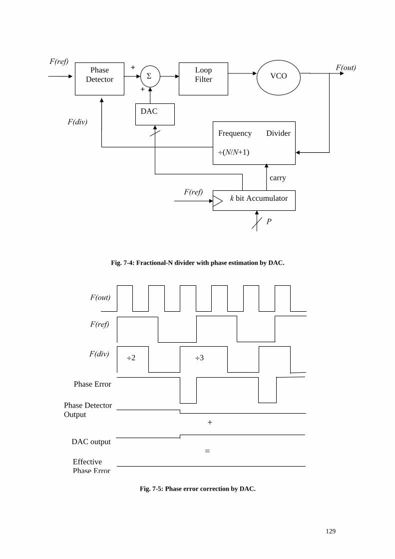
129
Fig. 7-4: Fractional-N divider with phase estimation by DAC.
Fig. 7-5: Phase error correction by DAC.
carry
+
+
P
F(ref)
F(out) Loop Filter
Frequency Divider
÷(N/N+1)
VCO
F(ref)
F(div)
Phase Detector
k bit Accumulator
DAC
Σ
Phase Detector Output
÷3
F(ref)
F(div)
F(out)
Phase Error
÷2
Effective Phase Error
DAC output
+
=

130
Since the phase error is subtracted in the voltage domain, this method suffers
from analog imperfections. This mismatch results primarily from the limited DAC
resolution and the limited accuracy and stability of the DAC. This approach gives the
best results when a sample-and-hold (S/H) phase detector is used. For the S/H phase
detector, the DAC needs to match only the dc voltage during one reference clock
period [111]. For other types of phase detectors, the DAC must generate a waveform
to match with the real-time phase detector output. A synthesizer that operates from
40 MHz to 51 MHz with a reference frequency of 100 kHz using this technique has
been reported to exhibit a resolution of 1 Hz and spurious sidebands typically less
than –70 dBc [5]. Another practical limitation for this technique is the difficulty in
implementing the DAC. For the standards such as the GSM and GPRS standards, a
large DAC (>25 bit DAC) is required to cover the entire frequency range with
reasonable accuracy [5].
7.2.2 Random Jittering
The spur in the fractional-N synthesizer originates from the fixed pattern of
the dual-modulus divider. This periodicity in the control sequence of the dual-
modulus divider can be eliminated by the random jitter injection [96].
While the phase estimation technique using a DAC operates in the analog
domain, this technique solves the spur problem in the digital domain. Fig. 7-6 shows a
block diagram of a fractional-N divider with random jittering [96]. At every output of
the divider, the random or pseudo-random number generator produces a new random
word Pn, which is compared with the frequency word k. If Pn is less than k, a division
by N is performed. If Pn is greater than k, a division by (N + 1) is performed. The

131
frequency word k controls the division by (N/N+1) so that the average value can track
the desired fractional division ratio.
The random jittering process generates a relatively high noise floor because
the injected phase jitter is white. It also suffers from frequency jitter because the white
noise injected in the frequency domain results in the 1/f2 noise in the phase domain
[96]. Since the PLL acts as a low-pass filter for the jitter generated by the fractional-N
divider, the low frequency components of the jitter will pass through the loop and
degrade the phase noise performance of the PLL synthesizer output.
Fig. 7-6: Fractional-N divider with random jittering.
k
Pn
Vvco
F(out) F(ref)
F(div)
Phase Detector
Loop Filter
Frequency Divider
÷(N/N+1)
VCO
Random Number Generator
N-bit Word Comparator
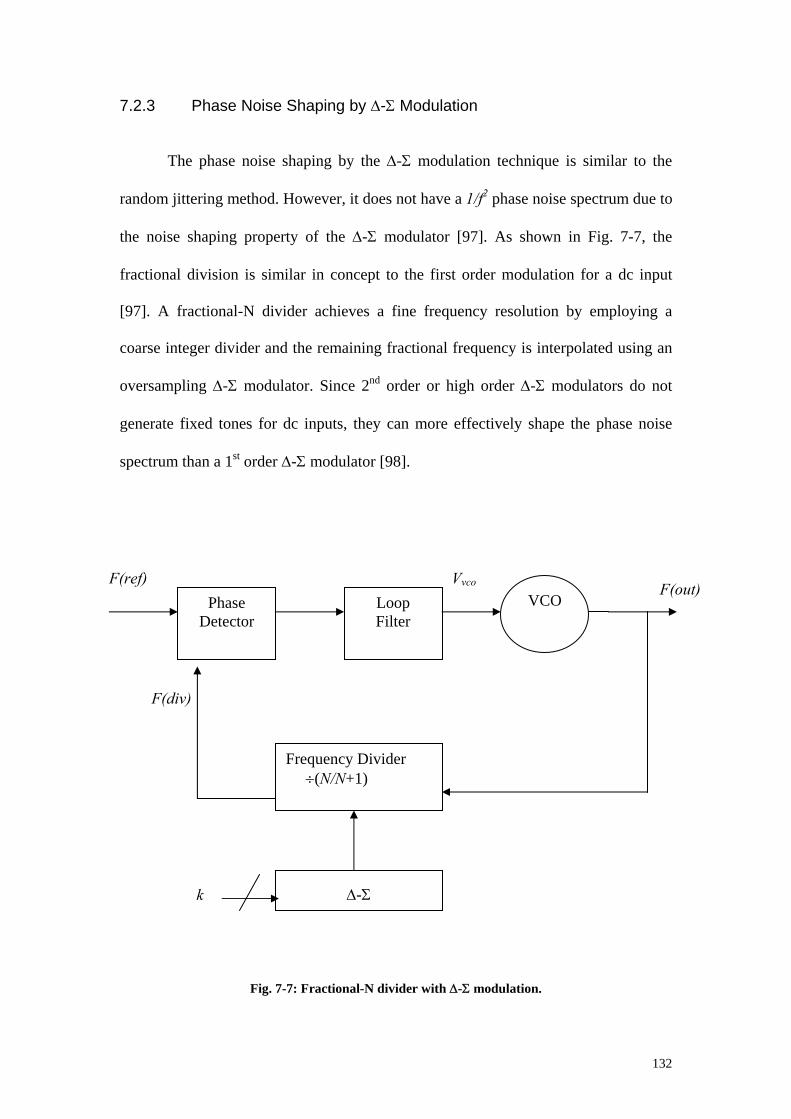
132
7.2.3 Phase Noise Shaping by ∆-Σ Modulation
The phase noise shaping by the ∆-Σ modulation technique is similar to the
random jittering method. However, it does not have a 1/f2 phase noise spectrum due to
the noise shaping property of the ∆-Σ modulator [97]. As shown in Fig. 7-7, the
fractional division is similar in concept to the first order modulation for a dc input
[97]. A fractional-N divider achieves a fine frequency resolution by employing a
coarse integer divider and the remaining fractional frequency is interpolated using an
oversampling ∆-Σ modulator. Since 2nd order or high order ∆-Σ modulators do not
generate fixed tones for dc inputs, they can more effectively shape the phase noise
spectrum than a 1st order ∆-Σ modulator [98].
Fig. 7-7: Fractional-N divider with ∆-Σ modulation.
Vvco
F(out) F(ref)
F(div)
Phase Detector
Loop Filter
Frequency Divider ÷(N/N+1)
VCO
∆-Σ k

133
Considering that the SNR determines the effective accuracy in oversampling
∆-Σ modulation, the unfiltered quantization noise may degrade the fractional division
accuracy [98]. The fractional division accuracy directly determines the carrier
frequency accuracy, which is required to be typically less than 10ppm in most systems.
The effective oversampling ratio can be defined by the ratio of the reference clock
frequency to the PLL bandwidth. By narrowing the bandwidth, the effective
oversampling ratio increases and the fractional division becomes more accurate.
When high-order ∆-Σ modulators are used, the PLL needs more poles in the loop filter
to suppress the quantization noise at high frequencies [97].
7.2.4 Phase Interpolation Technique
As an N-stage ring oscillator generates N different phases, which can be
applied to implement a fractional-N divider [29], combining a fixed divide-by-N
divider with the phase interpolation from a ring oscillator allows an N×k fractional
division. Fig. 7-8 shows an implementation of this type of fractional-N divider. Since
the number of inverters in a ring oscillator is limited by the operating frequency, a
phase interpolator should be used to generate finer phases from the limited phases
available from the VCO. By choosing the correct phases among the interpolated
phases, a fractional division is achieved.
Since the phase edges used for the fractional division are selected periodically,
inaccuracies in the interpolated phase edges generate fixed tones. Similar to the phase
estimation technique using a DAC, this architecture is also limited by analog
imperfections. The phase interpolation is performed by adding two adjacent phase
edges. If the slopes of the phase edges are too steep, there exists a timing uncertainty
due to the not-well-defined zero crossing. To avoid this timing uncertainty, the slope
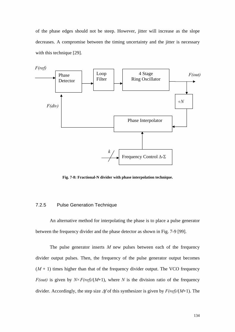
134
of the phase edges should not be steep. However, jitter will increase as the slope
decreases. A compromise between the timing uncertainty and the jitter is necessary
with this technique [29].
Fig. 7-8: Fractional-N divider with phase interpolation technique.
7.2.5 Pulse Generation Technique
An alternative method for interpolating the phase is to place a pulse generator
between the frequency divider and the phase detector as shown in Fig. 7-9 [99].
The pulse generator inserts M new pulses between each of the frequency
divider output pulses. Then, the frequency of the pulse generator output becomes
(M + 1) times higher than that of the frequency divider output. The VCO frequency
F(out) is given by N×F(ref)/(M+1), where N is the division ratio of the frequency
divider. Accordingly, the step size ∆f of this synthesizer is given by F(ref)/(M+1). The
k
F(out) F(ref)
F(div)
Phase Detector
Loop Filter
Frequency Control ∆-Σ
÷N
4 Stage Ring Oscillator
Phase Interpolator
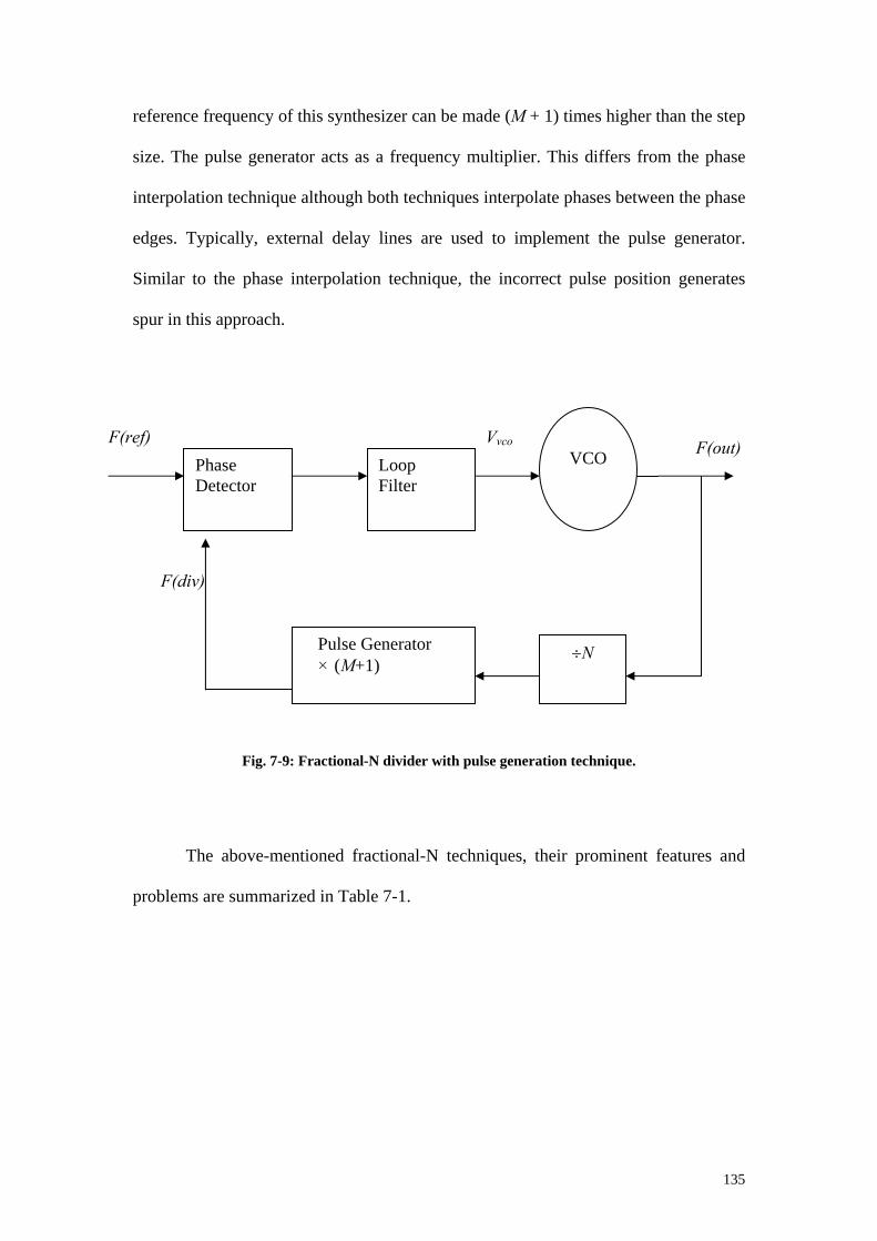
135
reference frequency of this synthesizer can be made (M + 1) times higher than the step
size. The pulse generator acts as a frequency multiplier. This differs from the phase
interpolation technique although both techniques interpolate phases between the phase
edges. Typically, external delay lines are used to implement the pulse generator.
Similar to the phase interpolation technique, the incorrect pulse position generates
spur in this approach.
Fig. 7-9: Fractional-N divider with pulse generation technique.
The above-mentioned fractional-N techniques, their prominent features and
problems are summarized in Table 7-1.
Vvco
F(out) F(ref)
F(div)
Phase Detector
Loop Filter
Pulse Generator × (M+1)
VCO
÷N
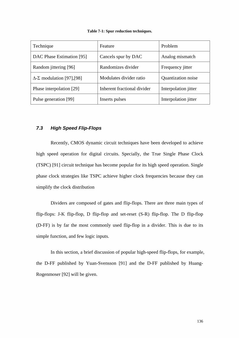
136
Table 7-1: Spur reduction techniques.
Technique Feature Problem
DAC Phase Estimation [95] Cancels spur by DAC Analog mismatch
Random jittering [96] Randomizes divider Frequency jitter
∆-Σ modulation [97],[98] Modulates divider ratio Quantization noise
Phase interpolation [29] Inherent fractional divider Interpolation jitter
Pulse generation [99] Inserts pulses Interpolation jitter
7.3 High Speed Flip-Flops
Recently, CMOS dynamic circuit techniques have been developed to achieve
high speed operation for digital circuits. Specially, the True Single Phase Clock
(TSPC) [91] circuit technique has become popular for its high speed operation. Single
phase clock strategies like TSPC achieve higher clock frequencies because they can
simplify the clock distribution
Dividers are composed of gates and flip-flops. There are three main types of
flip-flops: J-K flip-flop, D flip-flop and set-reset (S-R) flip-flop. The D flip-flop
(D-FF) is by far the most commonly used flip-flop in a divider. This is due to its
simple function, and few logic inputs.
In this section, a brief discussion of popular high-speed flip-flops, for example,
the D-FF published by Yuan-Svensson [91] and the D-FF published by Huang-
Rogenmoser [92] will be given.
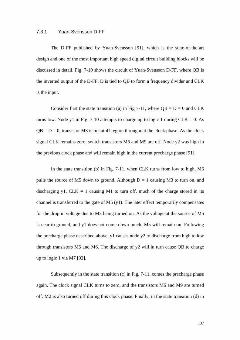
137
7.3.1 Yuan-Svensson D-FF
The D-FF published by Yuan-Svensson [91], which is the state-of-the-art
design and one of the most important high speed digital circuit building blocks will be
discussed in detail. Fig. 7-10 shows the circuit of Yuan-Svensson D-FF, where QB is
the inverted output of the D-FF, D is tied to QB to form a frequency divider and CLK
is the input.
Consider first the state transition (a) in Fig 7-11, where QB = D = 0 and CLK
turns low. Node y1 in Fig. 7-10 attempts to charge up to logic 1 during CLK = 0. As
QB = D = 0, transistor M3 is in cutoff region throughout the clock phase. As the clock
signal CLK remains zero, switch transistors M6 and M9 are off. Node y2 was high in
the previous clock phase and will remain high in the current precharge phase [91].
In the state transition (b) in Fig. 7-11, when CLK turns from low to high, M6
pulls the source of M5 down to ground. Although D = 1 causing M3 to turn on, and
discharging y1. CLK = 1 causing M1 to turn off, much of the charge stored in its
channel is transferred to the gate of M5 (y1). The later effect temporarily compensates
for the drop in voltage due to M3 being turned on. As the voltage at the source of M5
is near to ground, and y1 does not come down much, M5 will remain on. Following
the precharge phase described above, y1 causes node y2 to discharge from high to low
through transistors M5 and M6. The discharge of y2 will in turn cause QB to charge
up to logic 1 via M7 [92].
Subsequently in the state transition (c) in Fig. 7-11, comes the precharge phase
again. The clock signal CLK turns to zero, and the transistors M6 and M9 are turned
off. M2 is also turned off during this clock phase. Finally, in the state transition (d) in
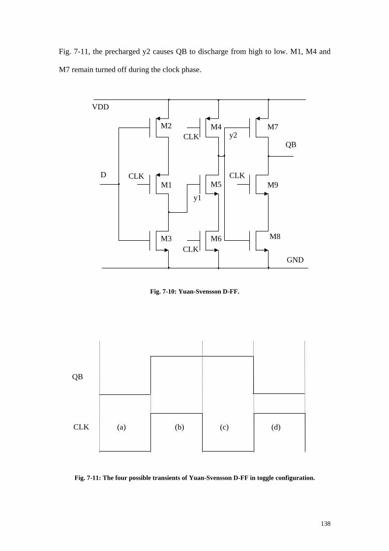
138
Fig. 7-11, the precharged y2 causes QB to discharge from high to low. M1, M4 and
M7 remain turned off during the clock phase.
Fig. 7-10: Yuan-Svensson D-FF.
Fig. 7-11: The four possible transients of Yuan-Svensson D-FF in toggle configuration.
CLK
QB
(d) (b) (a) (c)
M8
M9
M7 M4
M6 M3
M5 M1
M2
VDD
GND
QB
CLK
y2
y1
CLK
CLK
CLK D

139
7.3.2 Huang-Rogenmoser D-FF
Huang-Rogenmoser D-FF [92] is an improved version of Yuan-Svensson D-
FF, thus the operation principle of the Huang-Rogenmoser D-FF is similar to that of
Yuan-Svensson D-FF. Huang-Rogenmoser D-FF is a glitch free, general purpose,
high frequency D-FF with complementary outputs. In addition, Huang-Rogenmoser
D-FF can run at frequencies from tens of hertz to about a couple of gigahertz [92].
Fig. 7-12 shows the circuit diagram of Huang-Rogenmoser D-FF. M13 and M14 are
discharging transistors used to prevent the improper operation of the circuit at low
frequency [110]. M15 and M16 are deglitching transistors while M10 and M11 form
an inverter to provide an inversion of QB. The operations of the discharging transistor
and deglitching transistor are given in [92]. The details of the design of Huang-
Rogenmoser D-FF will be discussed in Section 7.4.
Fig. 7-12: Huang-Rogenmoser D-FF.
QB
D
VDD
GND
M1
M2
M3
M16
M15
M14
M4
M5
M6
M9
M12
M8
M7 M13
M11
M10
CLK CLK
CLK CLK Q
y1

140
7.3.3 Jan Craninckx’s D-FF
Jan Craninckx’s D-FF [94] is based on a standard Master and Slave ECL D-FF
[94]. The circuit exploits the speed enhancement by the reduction in voltage swing.
There are two disadvantages of this circuit. Firstly, the amplitude of the output signal
is approximately 0.7Vp-p operating at 2 GHz under a 3V supply [94]. Hence, an
amplifier might be needed to amplify the output signal, which increases the
complexity of the circuit and introduces extra delay to the frequency divider.
Secondly, an extra biasing voltage is needed in the circuit [94], which again increases
the complexity of the circuit and the power consumption.
7.4 Design of Frequency Divider
Due to the high frequency and wide range of operation, the design of the
frequency divider requires much attention. A frequency divider is designed such that
it is fast enough to operate at the highest frequency, and still be able to operate
properly at lower frequency, with the minimum power consumption. Fig. 7-13 shows
a divide-by-8 frequency divider. Huang-Rogenmoser D-FF is used as the basic
divide-by-2 circuit. The first two flip-flops, which are denoted as A in Fig. 7-13, are
optimized for the high speed. The last two flip-flops, which are denoted as B, are
optimized for the lower speed and minimum power consumption while still be able to
drive the load at the output of the divider.

141
Fig. 7-13: Frequency divider for divide-by-8 operation.
As mentioned previously, both Yuan-Svensson D-FF and Huang-Rogenmoser
D-FF are based on the TSPC circuit technique. An analogy between a dynamic TSPC
toggle-flip-flop and a three-inverter ring oscillator is shown in Fig. 7-14. The toggle-
flip-flop can be regarded as a three-inverter ring oscillator with some additional
control transistors that will regulate the oscillation frequency to about half of the input
frequency from the port CLK [28].
D
Q CLK
QB
A
D
QCLK
QB
A
D
QCLK
QB
B
D
QCLK
QB
B
Fin Fin/8

142
(a)
(b)
Fig. 7-14: Analogy between (a) dynamic TSPC CMOS toggle-flip-flop; and (b) three-inverter ring oscillator.
The design of the flip-flop needs a good understanding of the transistor model.
Fig. 7-15 shows the high frequency model of a MOS transistor [76], where gm is the
transistor transconducance, gs is the backgate transconductance, and rds is the drain-
M8
M9
M7 M4
M6 M3
M5 M1
M2
VDD
GND
QB
CLK
y2
y1
CLK
CLK
CLK
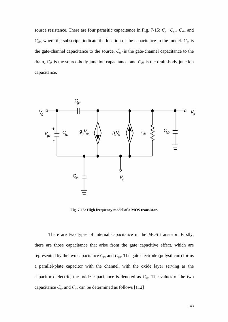
143
source resistance. There are four parasitic capacitance in Fig. 7-15: Cgs, Cgd, Csb, and
Cdb, where the subscripts indicate the location of the capacitance in the model. Cgs is
the gate-channel capacitance to the source, Cgd is the gate-channel capacitance to the
drain, Csb is the source-body junction capacitance, and Cdb is the drain-body junction
capacitance.
Fig. 7-15: High frequency model of a MOS transistor.
There are two types of internal capacitance in the MOS transistor. Firstly,
there are those capacitance that arise from the gate capacitive effect, which are
represented by the two capacitance Cgs and Cgd. The gate electrode (polysilicon) forms
a parallel-plate capacitor with the channel, with the oxide layer serving as the
capacitor dielectric, the oxide capacitance is denoted as Cox. The values of the two
capacitance Cgs and Cgd can be determined as follows [112]
rdsgsVsgmVgs
CdbCgs
Cgd
Vg
+
-Vgs
Csb Vs
Vd
144
1. For a MOS transistor operating in the triode region at small VDS, the channel
will have a uniform depth. The gate-channel capacitance will be WLCox and
can be modeled by dividing equally between the source and gate ends. Thus
OXgdgs WLCCC21
==
2. For a MOS transistor operating in the saturation region, the channel has a
tapered shape and is pinched off at or near the drain end. Thus, Cgd is zero
[113]
OXgs WLCC32
=
0=gdC
3. When the MOS transistor is in the cut off region, the channel disappears
0=gsC
0=gdC
4. The overlap capacitance Cov arises from the fact that the source and drain
diffusions extend slightly under the gate oxide. The overlap length is denoted
as Lov. The overlap capacitance should be added to Cgs and Cgd in all the
preceding formulas.
oxovov CWLC =
(7.2)
(7.3)
(7.4)
(7.5)
(7.6)
(7.7)

145
Secondly, the source-body and drain-body depletion-layer capacitance is
another type of internal capacitance, which are represented by Csb and Cdb. The source
body capacitance can be represented by
0
0
1 VVC
CSB
sbsb
+=
where Csb0 is the capacitance value of Csb at the zero reverse-bias voltage, VSB is the
magnitude of this reverse-bias voltage, and V0 is the junction built-in voltage.
Similarly for the drain diffusion, the drain-body capacitance Cdb can be represented by
0
0
1 VVC
CDB
dbdb
+=
where Cdb0 is the capacitance value at the zero reverse-bias voltage, and VDB is the
magnitude of this reverse-bias voltage. Note that it is assumed that for both junctions,
the grading coefficient m = 0.5 [112].
The circuit in Fig. 7-12 can be optimized using the design flow diagram as
shown in Fig. 7-16. The frequency divider is design to operate from 100 MHz to
1 GHz. The flow starts with the design of the first stage, which consists of M1, M2
and M3 to drive M5, M15 and M16. The second stage consists of discharging
transistor M14, as well as deglitching transistors M15 and M16. The third stage
consists of M4, M5 and M6, which drive M7 and M8. The fourth stage consists of M7,
M8, M9 and M12 to drive M10 and M11. The output stage consists of M10 and M11
to drive M1’, M4’, M6’ and M9’ of the next D-FF, as Q of the present D-FF is
connected to CLK of the next D-FF (refer to Fig. 7.13). In addition, the output stage
(7.8)
(7.9)
146
has a discharging transistor M13. The detailed calculations of the design will be
shown in the next section.
After designing the five stages, the frequency divider is verified through
simulation for the operation frequency from 100 MHz to 1 GHz. If the circuit fails to
operate at high frequency, optimization can be done by fine tuning the aspect ratios of
the transistors in the circuit. Generally, increasing the aspect ratio of the transistor will
decrease the delays in the signal path. However, this will eventually load the nodes in
the circuit. The parasitic capacitance of the transistors increases with their aspect
ratios, this in turn will slow down the circuit.
However, as general guidelines, M2 and M3 can be made smaller, as they only
drive M5, M15 and M16. M15 and M16 are deglitching transistors that require a
minimum aspect ratio [92], so their parasitic capacitance can be neglected. Effectively
the only load that M2 and M3 need to drive comes from M5. The size of M5 can be
increased to drive M7 and M8 faster. The sizes of M7 and M8 can be increased to
drive the output stage faster. The sizes should be adjusted in the mentioned order for
an optimum frequency performance.
If the circuit fails to operate at low frequencies due to the discharging of the
output nodes of each stage, the following guidelines are recommended. Firstly, to
increase the aspect ratios of the discharging transistors M13 and M14. Secondly, to
reduce the aspect ratios of M3, M4 and M7 as this will increase the output resistance
of the respective stages. When the circuit works properly, the layout can be done. The
LVS (layout versus schematic) and parasitic extraction process can be performed to
extract the parasitic introduced by the interconnections. The operation of the circuit is
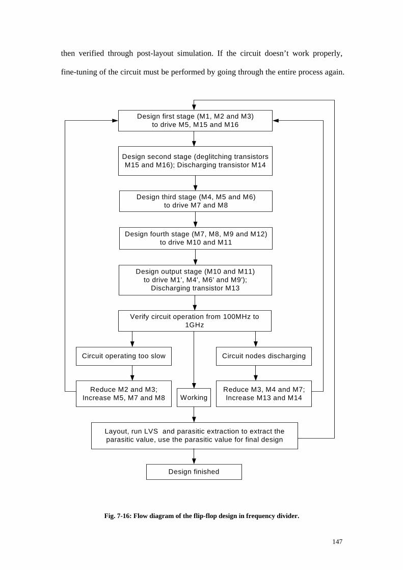
147
then verified through post-layout simulation. If the circuit doesn’t work properly,
fine-tuning of the circuit must be performed by going through the entire process again.
Fig. 7-16: Flow diagram of the flip-flop design in frequency divider.
Design first stage (M1, M2 and M3)to drive M5, M15 and M16
Design second stage (deglitching transistorsM15 and M16); Discharging transistor M14
Design third stage (M4, M5 and M6)to drive M7 and M8
Design fourth stage (M7, M8, M9 and M12)to drive M10 and M11
Design output stage (M10 and M11)to drive M1', M4', M6' and M9');
Discharging transistor M13
Verify circuit operation from 100MHz to1GHz
Circuit operating too slow
Working
Circuit nodes discharging
Reduce M2 and M3;Increase M5, M7 and M8
Reduce M3, M4 and M7;Increase M13 and M14
Layout, run LVS and parasitic extraction to extract theparasitic value, use the parasitic value for final design
Design finished
148
7.5 Detailed Calculations and Experimental Results
Following the design flow in Fig. 7-16, the frequency divider in Fig. 7-12 was
designed using the Chartered Semiconductor Manufacturing (CSM) 0.25µm
technology for GSM applications. The frequency divider was designed to operate
from 100 MHz to 1 GHz.
As mentioned previously, M15 and M16 are deglitching transistors, and M13
and M14 are discharging transistors. All these transistors are designed to have a
minimum aspect ratio to avoid overloading the circuit, which will affect the circuit
performance [92]. The aspect ratios of the PMOS transistors M16 and M13 are set to
0.5µm/0.25µm, while the aspect ratios of the NMOS transistors M15 and M14 are set
to 0.25µm/0.25µm.
Fig. 7-12 shows that the first stage of the flip-flop consists of M1, M2 and M3.
This stage is active when CLK is low. M1 acts as a switch to VDD, which is used to
power the M2-M3 inverter. As a rule of thumb, this inverter must drive the following
parasitic capacitors with a minimum of five times the maximum CLK frequency in
order to switch M5.
5gs5gd14db14gd16gs16gd
15gs15gd3db3gd2db2gd1p
CCCCCC
CCCCCCC
+++++
++++++=
Note that although some of the transistors are actually in the cut off region, the
parasitic capacitance of those transistors is calculated assuming the transistors are in
the saturation region, this will guarantee the operation of circuit at the high speed.
This parasitic capacitance is approximated to be 40fF. Through equation (7.11), it can
be approximated that a switching current of 2.5mA is needed to charge the parasitic
(7.10)
149
capacitor in 32psec to switch M5. This ensures that the flip-flop will operate at the
maximum CLK frequency of 1GHz.
VCtI ×=×
where I is the switching current, t is the charging time, C is the node parasitic
capacitance, and V is the voltage swing at the node. The aspect ratio of M3 is
calculated as follows
µ.µ..
).-(µA/VmA).(
)(VDD-VCµI
LW
tnoxn
25012358
6102310522
2
22
23
≈=
×=
=⎟⎠⎞
⎜⎝⎛
wherer µn, Cox, Vtn are the NMOS transistor mobility, oxide capacitance and threshold
voltage, respectively. M2 is designed for a symmetrical output drive. For simplicity,
assume Vtn = −Vtp
µ.µ.
µ.µ..
µ.µ.
VµAVµA
LW
CµCµ
LW
oxp
oxn
25085
2501272
25012
115310
2
2
32
=⎟⎟⎠
⎞⎜⎜⎝
⎛≈
⎟⎟⎠
⎞⎜⎜⎝
⎛=
⎟⎠⎞
⎜⎝⎛=⎟
⎠⎞
⎜⎝⎛
For high operating frequencies, the aspect ratio of M1 needs to be large to
supply the current to charge-up the inverter. In addition, M1 and M2 are in series, the
delay to charge up the inverter is longer than the delay in a single transistor, so the
aspect ratio of M1 needs to be larger. However, the charge time is not critical in the
(7.11)
(7.12)
(7.13)

150
lower frequency flip-flop B, the size of M1 in flip-flop B is chosen to be half of the
size of M1 in flip-flop A for optimum performance
µ.µ
LW,
µ.µ
LW
BA 2503
2506
11
=⎟⎠⎞
⎜⎝⎛=⎟
⎠⎞
⎜⎝⎛
Fig. 7-12 shows the second stage consisting of the discharging transistor M14,
as well as the deglitching transistors M15 and M16. The aspect ratios of these
transistors are
µ.µ.
LW,
µ.µ.
LW,
µ.µ.
LW
25050
250250
250250
161514
=⎟⎠⎞
⎜⎝⎛=⎟
⎠⎞
⎜⎝⎛=⎟
⎠⎞
⎜⎝⎛
Fig. 7-12 shows the third stage consisting of M4, M5 and M6. This stage is
active when CLK is high. M4 precharges the output of this stage to VDD when CLK
is low. When CLK goes high, M6 supplies power to M5, which turns the voltage at
the node y2 to low. As a rule of thumb, M5 must drive the following parasitic
capacitors with a minimum of five times the maximum CLK frequency in order to
switch M7 and M8.
887744552 gdgsgdgsdbgddbgdp CCCCCCCCC +++++++=
Cp2 is estimated to be 100fF. A switching current of 6.25mA is needed to
charge the parasitic capacitor in 32psec to switch M7 and M8. This ensures that the
flip-flop will operate at the maximum CLK frequency of 1 GHz. Thus the aspect ratio
for M5 is
(7.14)
(7.15)
(7.16)

151
µ.µ.
).-(VµAmA).(
)(VDD-VCµI
LW
tnoxn
25025521
61023102562
2
22
25
≈=
=
=⎟⎠⎞
⎜⎝⎛
For high operating frequencies, the aspect ratios of M4 and M6 need to be
large to supply the current to charge their drain nodes quickly. Since the charging
time is not critical for the lower frequency flip-flop B, the sizes of M4 and M6 can be
smaller. Thus, the size of M4 and M6 are designed to be
µ.µ.
LW,
µ.µ.
LW
BA 250753
25057
44
=⎟⎠⎞
⎜⎝⎛=⎟
⎠⎞
⎜⎝⎛
µ.µ
LW,
µ.µ
LW
BA 2503
2506
66
=⎟⎠⎞
⎜⎝⎛=⎟
⎠⎞
⎜⎝⎛
The fourth stage consists of M7, M8, M9 and M12 to drive M10 and M11.
This stage is active when CLK is high. M9 acts as a switch to GND, which is used to
power the inverter formed by M7 and M8. This inverter must drive the following
parasitic capacitors with a minimum of five times the maximum CLK frequency in
order to switch M10, M11, M2 and M3.
33221111
101088773
gdgsgdgsgdgs
gdgsdbgddbgdp
CCCCC C
CCCCCCC
+++++
++++++=
Cp3 is estimated to be 100fF. A switching current of 6.25mA is needed to
charge the parasitic capacitor in 32psec to ensure that the flip-flop will operate at the
maximum CLK frequency of 1 GHz. For the lower frequency flip-flop B, about
(7.17)
(7.18)
(7.20)
(7.19)
152
3.125mA is needed to charge the parasitic capacitor in about 64psec. Thus the aspect
ratio for M8 is
µm.µm.
).-)(µA/V(mA).(
)(VDD-VCµI
LW
tnoxnA
25025521
61023102562
2
22
28
≈=
=
=⎟⎠⎞
⎜⎝⎛
and µ.µ.
LW
B 25072
8
=⎟⎠⎞
⎜⎝⎛
Since M7 is designed for a symmetrical output drive. The aspect ratio of M7 is
thus
µ.µ.
µ.µ..
µ.µ.
VµAVµA
LW
CµCµ
LW
oxp
oxn
A
250214
25025572
250255
115310
2
2
87
=⎟⎟⎠
⎞⎜⎜⎝
⎛≈
⎟⎟⎠
⎞⎜⎜⎝
⎛=
⎟⎠⎞
⎜⎝⎛=⎟
⎠⎞
⎜⎝⎛
and µ.µ.
LW
B 25027
7
=⎟⎠⎞
⎜⎝⎛
For high operating frequencies, the aspect ratios of M9 and M12 need to be
large to supply the current to charge their drain nodes quickly. Thus, the sizes of M9
and M12 are designed to be
µ.µ.
LW,
µ.µ.
LW
BA 25063
25027
99
=⎟⎠⎞
⎜⎝⎛=⎟
⎠⎞
⎜⎝⎛
µ.µ.
LW,
µ.µ.
LW
BA 25063
25027
1212
=⎟⎠⎞
⎜⎝⎛=⎟
⎠⎞
⎜⎝⎛
(7.21)
(7.23)
(7.22)

153
The output stage consists of M13 and an inverter formed by M10 and M11.
This inverter must drive the following parasitic capacitors with a minimum of five
times the maximum CLK frequency in order to switch M1, M4, M6 and M9.
996644
11111110104
gdgsgdgsgdgs
gdgsdbgddbgdp
CCCCCC
CCCCCCC
+++++
++++++=
Cp4 is estimated to be 100fF. A switching current of 6.25mA is needed to
charge the parasitic capacitor in 32psec to ensure that the flip-flop will operate at the
maximum CLK frequency of 1GHz. Thus the aspect ratio of M11 is
µ.µ.
).-)(µA/V(mA).(
)(VDD-VCµI
LW
tnoxn
25025521
61023102562
2
22
211
≈=
=
=⎟⎠⎞
⎜⎝⎛
Since M10 is designed for a symmetrical output drive. The aspect ratio of M10
is thus
µ.µ.
µ.µ..
µ.µ.
VµAVµA
LW
CµCµ
LW
oxp
oxn
250214
25025572
250255
115310
2
2
1110
=⎟⎟⎠
⎞⎜⎜⎝
⎛≈
⎟⎟⎠
⎞⎜⎜⎝
⎛=
⎟⎠⎞
⎜⎝⎛=⎟
⎠⎞
⎜⎝⎛
While the aspect ratio of the discharging transistor M13 is
µ.µ.
LW
25050
13
=⎟⎠⎞
⎜⎝⎛
(7.24)
(7.25)
(7.26)
(7.27)
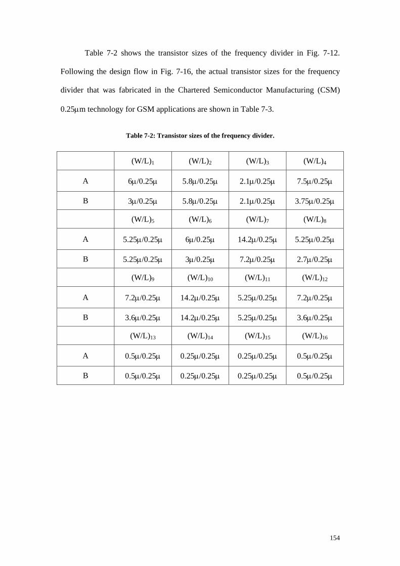
154
Table 7-2 shows the transistor sizes of the frequency divider in Fig. 7-12.
Following the design flow in Fig. 7-16, the actual transistor sizes for the frequency
divider that was fabricated in the Chartered Semiconductor Manufacturing (CSM)
0.25µm technology for GSM applications are shown in Table 7-3.
Table 7-2: Transistor sizes of the frequency divider.
(W/L)1 (W/L)2 (W/L)3 (W/L)4
A 6µ/0.25µ 5.8µ/0.25µ 2.1µ/0.25µ 7.5µ/0.25µ
B 3µ/0.25µ 5.8µ/0.25µ 2.1µ/0.25µ 3.75µ/0.25µ
(W/L)5 (W/L)6 (W/L)7 (W/L)8
A 5.25µ/0.25µ 6µ/0.25µ 14.2µ/0.25µ 5.25µ/0.25µ
B 5.25µ/0.25µ 3µ/0.25µ 7.2µ/0.25µ 2.7µ/0.25µ
(W/L)9 (W/L)10 (W/L)11 (W/L)12
A 7.2µ/0.25µ 14.2µ/0.25µ 5.25µ/0.25µ 7.2µ/0.25µ
B 3.6µ/0.25µ 14.2µ/0.25µ 5.25µ/0.25µ 3.6µ/0.25µ
(W/L)13 (W/L)14 (W/L)15 (W/L)16
A 0.5µ/0.25µ 0.25µ/0.25µ 0.25µ/0.25µ 0.5µ/0.25µ
B 0.5µ/0.25µ 0.25µ/0.25µ 0.25µ/0.25µ 0.5µ/0.25µ

155
Table 7-3: Actual transistor sizes of the frequency divider.
(W/L)1 (W/L)2 (W/L)3 (W/L)4
A 7.5µ/0.25µ 6.5µ/0.25µ 2.25µ/0.25µ 6.25µ/0.25µ
B 3.75µ/0.25µ 6.5µ/0.25µ 2.25µ/0.25µ 3.12µ/0.25µ
(W/L)5 (W/L)6 (W/L)7 (W/L)8
A 5.75µ/0.25µ 6.25µ/0.25µ 8µ/0.25µ 5µ/0.25µ
B 5.75µ/0.25µ 3.125µ/0.25µ 4µ/0.25µ 2.5µ/0.25µ
(W/L)9 (W/L)10 (W/L)11 (W/L)12
A 7.5µ/0.25µ 10µ/0.25µ 5µ/0.25µ 6.25µ/0.25µ
B 3.75µ/0.25µ 10µ/0.25µ 5µ/0.25µ 3.12µ/0.25µ
(W/L)13 (W/L)14 (W/L)15 (W/L)16
A 1µ/0.25µ 0.5µ/0.25µ 0.5µ/0.25µ 1µ/0.25µ
B 1µ/0.25µ 0.5µ/0.25µ 0.5µ/0.25µ 1µ/0.25µ
Fig. 7-17 shows the microphotograph of the frequency divider, which
performs a divide-by-8 operation. Measured results of the frequency divider are
shown in Fig. 7-18.
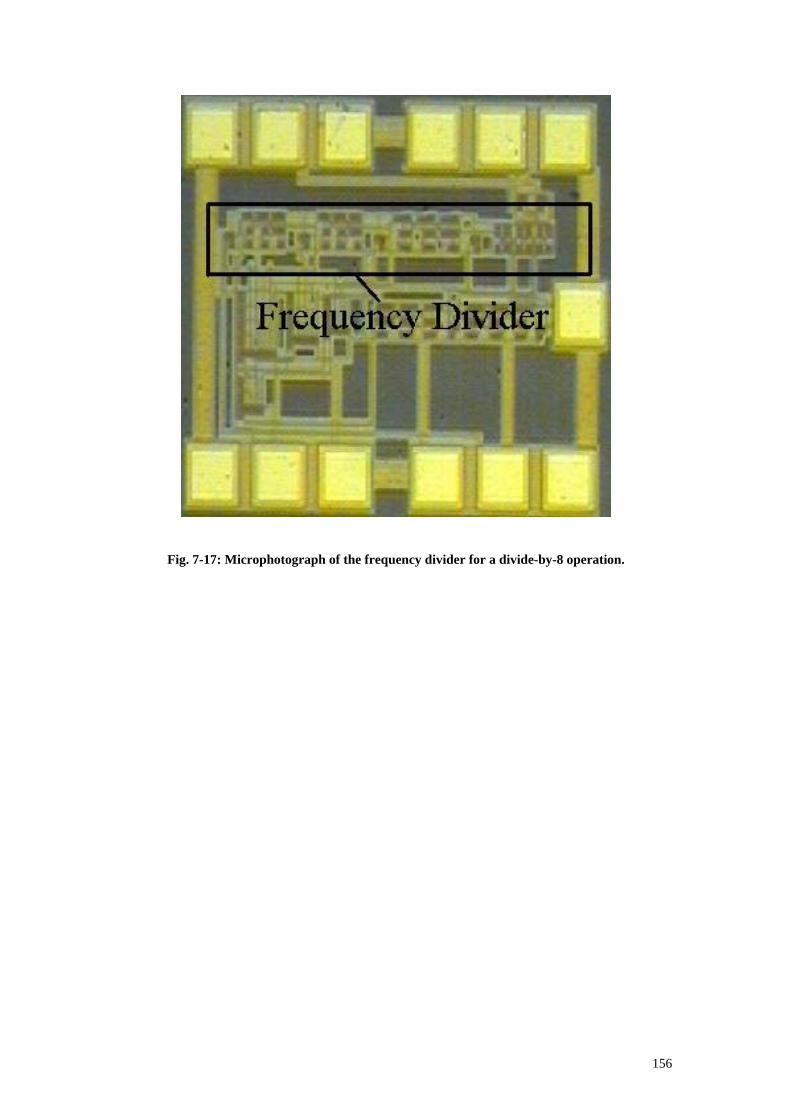
156
Fig. 7-17: Microphotograph of the frequency divider for a divide-by-8 operation.
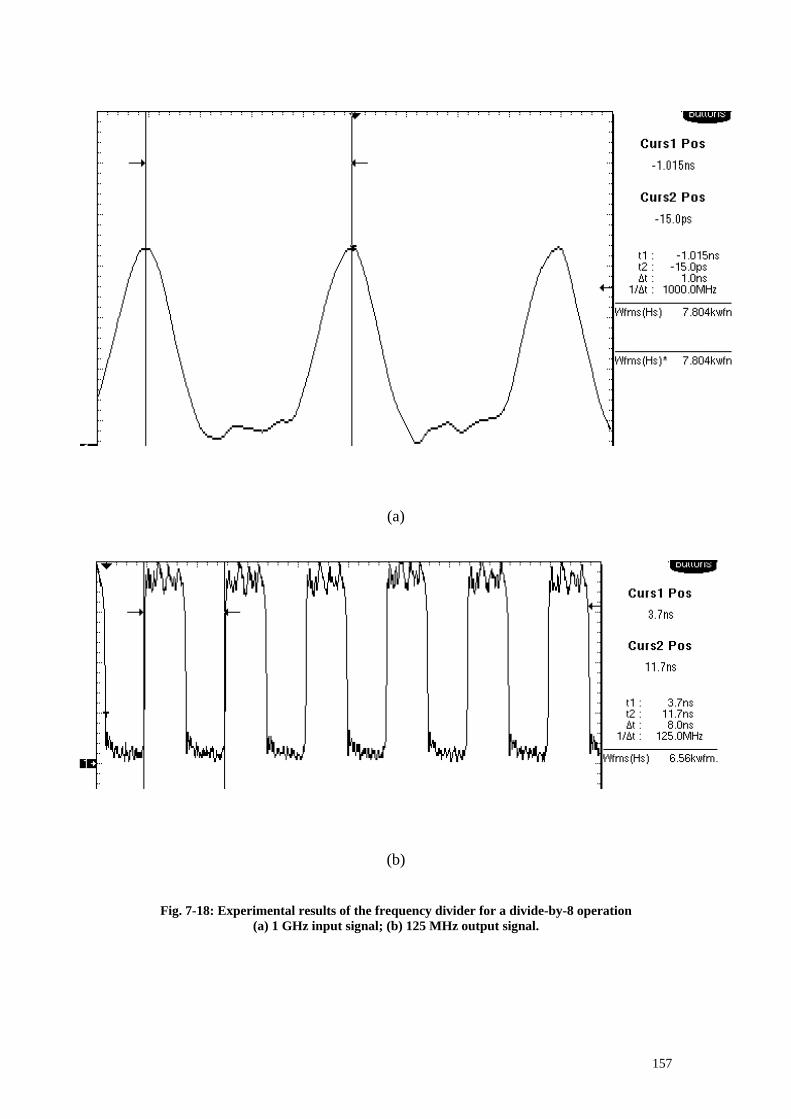
157
(a)
(b)
Fig. 7-18: Experimental results of the frequency divider for a divide-by-8 operation (a) 1 GHz input signal; (b) 125 MHz output signal.

158
7.6 Summary
In this chapter, a review of various spur reduction techniques was presented.
The design of high-speed frequency dividers was discussed. The measured results for
the implemented frequency divider were shown.
In Chapter 8, a novel spur reduction fractional-N frequency divider with a
frequency range, which is 3.5 times larger than that of a conventional fractional-N
divider, will be presented. In Chapter 9, a novel technique that can fully suppress the
fractional spur for fractional-N frequency synthesizer will be presented.
159
CHAPTER 8
Fully Integrated CMOS Fractional-N Frequency
Divider for Wide-Band Mobile Applications
with Spur Reduction
The fractional-N frequency divider has become increasingly popular in RF
applications as it allows PLL Synthesizers to have a frequency resolution finer than
the reference frequency. However, there are two main disadvantages of a fractional-N
divider, namely, fractional spur generation and frequency range limitation. A
fractional-N divider generates fractional spur due to the fixed pattern of the dual-
modulus divider [7]. The frequency range of a fractional-N divider is equal to its
reference frequency. This limits its usefulness especially in wide-band applications.
A dual-band PLL synthesizer for personal communications services (PCS)-
and cellular- code division multiple access (CDMA) systems is demonstrated in [7].
This circuit uses a charge-averaging charge pump to solve the fractional spur problem.
However, this approach is only suitable for a small number of division ratios as it is
limited by the complexity of the charge pump. As the frequency range of a dual-
modulus fractional-N frequency synthesizer is equal to the reference frequency, e.g.
19.8 MHz as in [7], the operating band may not be fully covered.
This chapter describes a new technique for reducing the fractional spur while
providing a wide frequency range. The width of the maximum phase error’s pulse
[100] in the new design is less than a quarter of that of the conventional one. This is
achieved through the introduction of a new division ratio (N + 1/4) in the divider. This

160
frequency divider has a frequency range of 3.5 times larger than that of the
conventional fractional-N divider, as its division modulus ranges from (N-1.75) to
(N+1.75) while a conventional fractional-N divider has only a division modulus of N
to (N+1). This technique also reduces the magnitude of the fractional spur to one
quarter of the usual value.
In the modern transceiver design, the quadrature VCO is often needed to
generate the quadrature signals for the LO inputs of either image-reject mixers [62] or
frequency down converters with I/Q outputs. For multiple standard applications, the
VCO needs to have a wide tuning range in order to cover the entire range of operation
frequency. The quadrature VCOs reported in [66] and [61] have a wide tuning range
of 18.5% and 24%, respectively. The results show that the quadrature VCO is a good
candidate for multiple standard applications. As the quadrature VCO is becoming
more popular in modern communication systems [53],[61],[64]-[66],[70]-[73], these
quadrature outputs are used in this new frequency synthesizer.
8.1 Frequency Divider Topology
In a fractional-N frequency divider, a dual-modulus divider, divide-by-(N/N+1)
is used. The fractional division is obtained by periodically changing the division ratio.
To achieve a divide-by-4.125 operation, seven divide-by-4 operations followed by
one divide-by-5 operation are required. As shown in Fig. 8-1, each of the first seven
cycles of the divided signal is slightly shorter than the reference period. Consequently,
the phase error between the reference and the feedback signal grows in every period
of F(ref) till it returns to zero when the divide-by-5 operation occurs. Thus, the phase
detector produces progressively wider error pulses, creating a ramp at the filter output
of the PLL.

161
Here, it can be concluded that if the VCO output is to be equal to
(N + α)F(ref), (e.g., α = 1/8 and N = 4 in Fig. 8-1), the output of the low pass filter
(LPF) will be a repetitive ramp waveform with a period of 1/(αF(ref)). If the loop is
closed, such a waveform would modulate the VCO, creating sidebands at αF(ref),
2αF(ref), etc. with respect to the center frequency. Such sidebands are called
fractional spur. For example, for α = 1/8, the output of the LPF will be a periodic
ramp waveform with a period of 8/F(ref), creating sidebands at 0.125F(ref),
0.25F(ref), etc. with respect to the center frequency.
Fig. 8-1: Effect of unequal instantaneous frequencies.
The new fractional-N frequency divider with (N + 1/4) modulus is shown in
Fig. 8-2. The operation of the (N + 1/4) division fractional-N frequency divider will
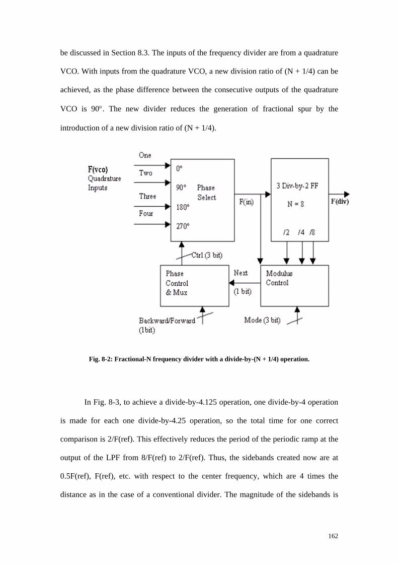
162
be discussed in Section 8.3. The inputs of the frequency divider are from a quadrature
VCO. With inputs from the quadrature VCO, a new division ratio of (N + 1/4) can be
achieved, as the phase difference between the consecutive outputs of the quadrature
VCO is 90°. The new divider reduces the generation of fractional spur by the
introduction of a new division ratio of (N + 1/4).
Fig. 8-2: Fractional-N frequency divider with a divide-by-(N + 1/4) operation.
In Fig. 8-3, to achieve a divide-by-4.125 operation, one divide-by-4 operation
is made for each one divide-by-4.25 operation, so the total time for one correct
comparison is 2/F(ref). This effectively reduces the period of the periodic ramp at the
output of the LPF from 8/F(ref) to 2/F(ref). Thus, the sidebands created now are at
0.5F(ref), F(ref), etc. with respect to the center frequency, which are 4 times the
distance as in the case of a conventional divider. The magnitude of the sidebands is
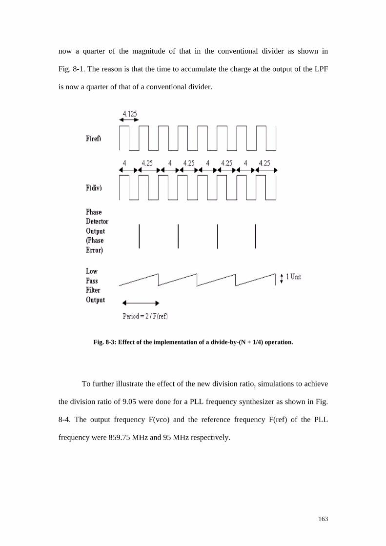
163
now a quarter of the magnitude of that in the conventional divider as shown in
Fig. 8-1. The reason is that the time to accumulate the charge at the output of the LPF
is now a quarter of that of a conventional divider.
Fig. 8-3: Effect of the implementation of a divide-by-(N + 1/4) operation.
To further illustrate the effect of the new division ratio, simulations to achieve
the division ratio of 9.05 were done for a PLL frequency synthesizer as shown in Fig.
8-4. The output frequency F(vco) and the reference frequency F(ref) of the PLL
frequency were 859.75 MHz and 95 MHz respectively.
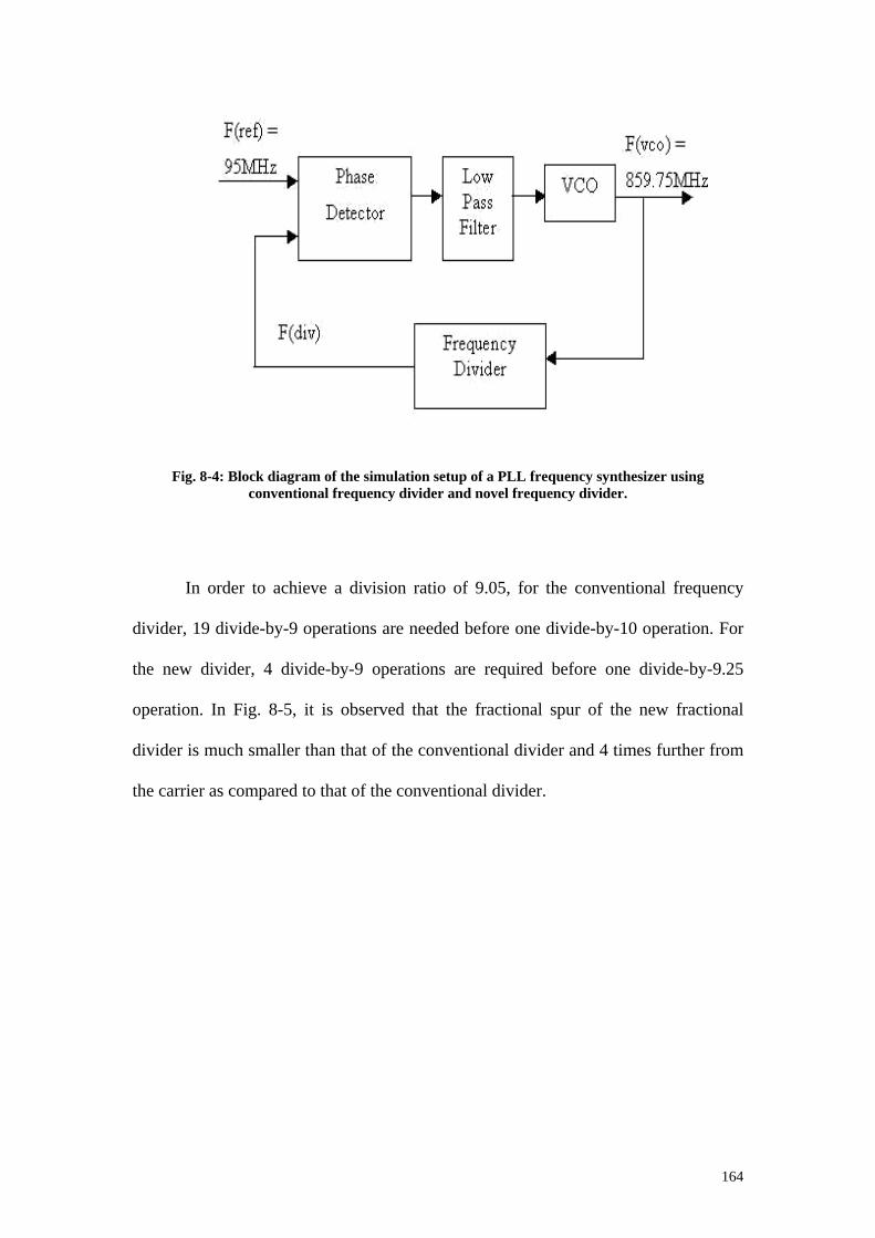
164
Fig. 8-4: Block diagram of the simulation setup of a PLL frequency synthesizer using conventional frequency divider and novel frequency divider.
In order to achieve a division ratio of 9.05, for the conventional frequency
divider, 19 divide-by-9 operations are needed before one divide-by-10 operation. For
the new divider, 4 divide-by-9 operations are required before one divide-by-9.25
operation. In Fig. 8-5, it is observed that the fractional spur of the new fractional
divider is much smaller than that of the conventional divider and 4 times further from
the carrier as compared to that of the conventional divider.
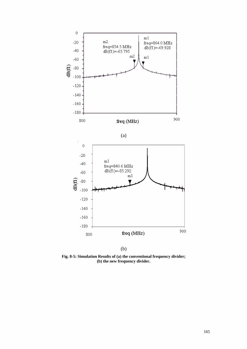
165
(a)
(b) Fig. 8-5: Simulation Results of (a) the conventional frequency divider;
(b) the new frequency divider.

166
8.2 Circuit Description
8.2.1 Modulus Control
Fig. 8-6 shows the modulus control circuitry. The 3-bit division modulus
control word, Mode, determines the modulus of a division by generating 1, or 2 or 4
pulses depending on the settings of the control bits Mode1, Mode2 and Mode3. For
example, when Mode is 100, where Mode3 is high, while Mode1 and Mode2 are low,
four pulses will be generated at the output Next [94]. The inputs F(in), /2, /4 and /8
correspond to the outputs of the phase select, and the three divide-by-2 flip-flop
outputs respectively as shown in Fig. 8-2.
Fig. 8-6: Modulus control circuitry.

167
8.2.2 Phase Control Circuitry
The phase control circuitry is needed to convert the signal Next generated
from the modulus control circuitry to the 3-bit Control Signal in the phase select
circuitry. The 3-bit control signal Ctrl is generated by the two divide-by-2 flip-flops as
shown in Fig. 8-7.
Fig. 8-7: Phase control circuitry.
8.2.3 Phase Select
A phase select circuitry is needed to switch the inputs from One to Two, Two
to Three, Three to Four and then back from Four to One, whenever the Ctrl signal
changes. The multiplexer in the phase select circuitry is implemented using pass
transistors as shown in Fig. 8-8. In this design, Control 1 and Control 2 are the same
signal, so they can be combined into a single bit. When Ctrl is equal to 11 (Control
1/2 Control 3), the output of the phase select circuitry F2 is connected to One. If Ctrl
is 10, F2 is connected to Two. If Ctrl is 01, F2 is connected to Three. Lastly, when
Ctrl is 00, F2 is connected to Four.

168
Fig. 8-8: Phase select circuitry.
8.3 Circuit Operation
For forward propagation division, the new divider operates as follows. As
shown in Fig. 8-2, the input signals namely, One, Two, Three and Four, are fed to the
phase select circuitry. When the 3-bit signal Mode is 000, the phase control block is
disabled and its output signal F(in) is not changed. This means that the output of the
multiplexer will be taken from the same input as the previous clock. Hence, F(div) is
8 times smaller than the input frequency F(in). Depending on the required modulus,
the control signal Ctrl will change in such a way that the division control block will
connect F(in) to the signal that is 90° phase shifted with respect to the present signal,
e.g. from 0° to 90° or 90° to 180°. For example, for a division of 8.25, Mode is equal
to 001. Hence, one pulse will be generated at Next. If F(in) is initially connected to
One, after Ctrl changes, a connection will be made to Two. Hence, a division of 8.25
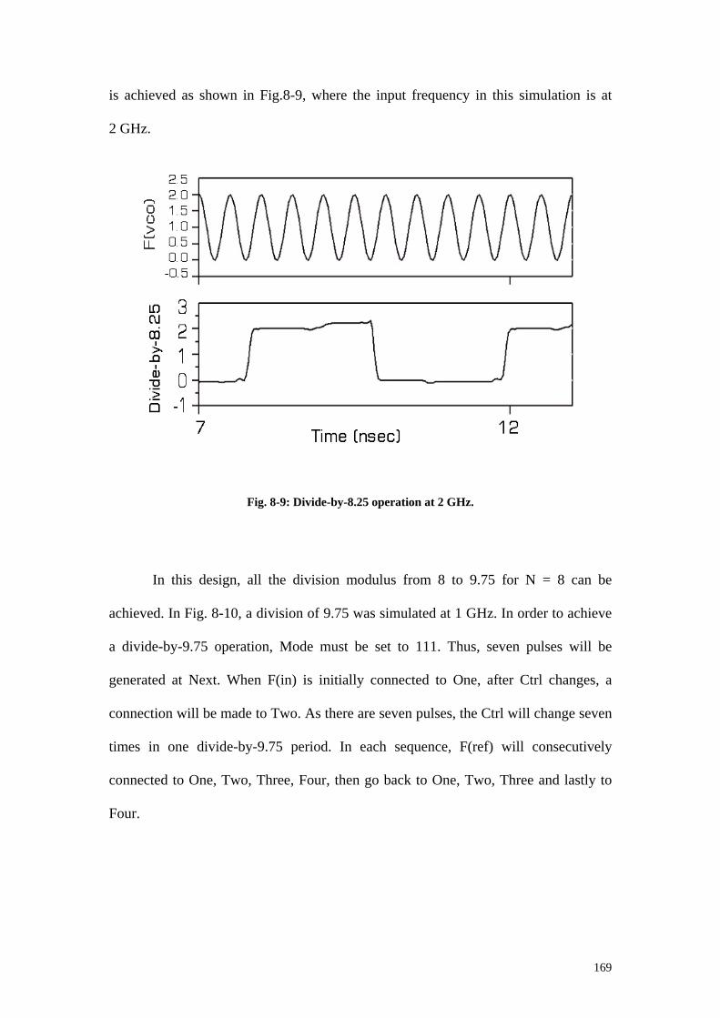
169
is achieved as shown in Fig.8-9, where the input frequency in this simulation is at
2 GHz.
Fig. 8-9: Divide-by-8.25 operation at 2 GHz.
In this design, all the division modulus from 8 to 9.75 for N = 8 can be
achieved. In Fig. 8-10, a division of 9.75 was simulated at 1 GHz. In order to achieve
a divide-by-9.75 operation, Mode must be set to 111. Thus, seven pulses will be
generated at Next. When F(in) is initially connected to One, after Ctrl changes, a
connection will be made to Two. As there are seven pulses, the Ctrl will change seven
times in one divide-by-9.75 period. In each sequence, F(ref) will consecutively
connected to One, Two, Three, Four, then go back to One, Two, Three and lastly to
Four.
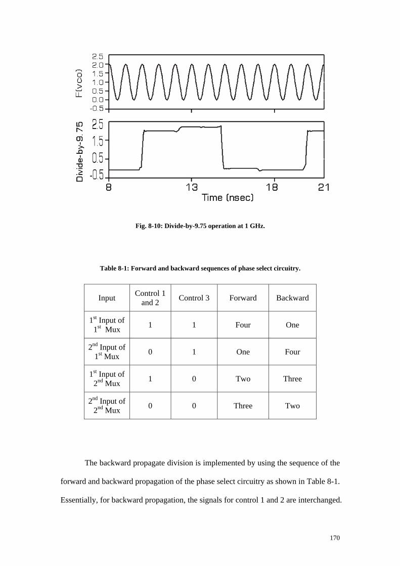
170
Fig. 8-10: Divide-by-9.75 operation at 1 GHz.
Table 8-1: Forward and backward sequences of phase select circuitry.
Input Control 1 and 2 Control 3 Forward Backward
1st Input of 1st Mux 1 1 Four One
2nd Input of 1st Mux 0 1 One Four
1st Input of 2nd Mux 1 0 Two Three
2nd Input of 2nd Mux 0 0 Three Two
The backward propagate division is implemented by using the sequence of the
forward and backward propagation of the phase select circuitry as shown in Table 8-1.
Essentially, for backward propagation, the signals for control 1 and 2 are interchanged.

171
Hence, the range of the division ratio for the prescaler is increased by two times,
which ranges from (N − 1.75) = 6.25 to (N + 1.75) = 9.75 for N=8.
8.4 Experimental Results
The frequency divider of Fig. 8-2 was designed and fabricated using the
CMOS 0.25µm process. A 1.2 GHz frequency quadrature VCO was designed to
generate the quadrature signals into the frequency divider. The quadrature VCO was
designed using the parasitic-compensated quadrature VCO technique discussed in
Chapter 4. The active chip area is 1200µm x 1600µm. The divider and the quadrature
VCO consume 9mW at 2V supply, where 3mW is for the frequency divider and 6mW
is for the quadrature VCO. Fig. 8-11 shows a microphotograph of the frequency
divider with the quadrature VCO.
FrequencyDivider
QuadratureVCO
Fig. 8-11: Microphotograph of the frequency divider and 1.2 GHz quadrature VCO.

172
Fig. 8-12 shows the power spectrum of the VCO output at 1.2 GHz. A divide-
by-9.75 operation is implemented through forward propagation of the phase select
circuitry, which results in an output frequency of 1.2 GHz/9.75 = 123.1 MHz. A
divide-by-7.75 operation is implemented through backward propagation of the phase
select circuitry, which results in an output frequency of 1.2 GHz/7.75 = 154.8 MHz.
Fig. 8-13 and Fig. 8-14 show the power spectrums of the divider output at 123.1 MHz
and 154.8 MHz, respectively.
Fig. 8-12: Power spectrum of the VCO output at 1.2 GHz.

173
Fig. 8-13: Power spectrum of the frequency divider output at 123.1 MHz.
Fig. 8-14: Power spectrum of the frequency divider output at 154.8 MHz.

174
8.5 Summary
A new multiple modulus (N + 1/4) fractional-N frequency divider was
presented. This frequency divider provides a new division of (N + 1/4), which reduces
the generation of fractional spur. In addition, it has a large range of multiple modulus
division from (N - 1.75) to (N + 1.75), as shown in the above example it ranges from
6.25 to 9.75 for N = 8. This will enable the frequency divider to support multiple
standard applications for fixed and mobile radios that operate over a wide range of
frequency. This work was published in [114].

175
CHAPTER 9
A New Spur Reduction Fractional-N
Frequency Divider
In this chapter, another method to overcome the fractional spur generated by
the fractional-N technique is introduced. In the previous chapter, a spur reduction
technique, which greatly reduced the magnitude of the fractional spur and at the same
time increased the division modulus range, has been introduced. In comparison, this
method eliminates the fractional spur generated. Furthermore, it has the advantage of
simplicity where it needs only two extra 2-to-1 multiplexers.
9.1 Circuit Description
In a conventional fractional-N frequency divider, a dual-modulus divider,
divide-by-(N/N+1), is used. The fractional division is obtained by periodically
changing the division value. To achieve a divide-by-461 operation, five divide-by-4
operations are done before one divide-by-5 operation. The carry of the accumulator in
Fig. 9-1 is in the sequence of 000001000001…, where a division by (N + 1) is
corresponding to “1”.
As shown in Fig. 9-2, each of the first five cycles of the divided signal is
slightly shorter than the reference period. Consequently, the phase difference between
the reference and the feedback signal grows in every period of reference frequency
F(ref) till it returns to zero when the divide-by-5 operation occurs. Thus, the phase
detector produces progressively wider pulses, creating a ramp waveform at the output
of the loop filter.

176
Fig. 9-1: A conventional fractional-N frequency divider.
Fig. 9-2: Effect of unequal instantaneous frequencies in a fractional-N synthesizer.
Phase Detector Output

177
Here, it can be concluded that if the VCO output frequency is to be equal to
(N + α)F(ref), (e.g., α = 1/6 and N = 4 in Fig. 9-2), the output of the loop filter (LF)
will be a repetitive ramp waveform with a period 1/(αF(ref)).
If the loop was closed, such a waveform would modulate the VCO, creating
sidebands at αF(ref), 2αF(ref), etc. with respect to the center frequency. Such
sidebands are called fractional spur.
Fig. 9-3 shows the proposed spur reduction frequency divider. A 2-to-1
multiplexer is used to select between F(ref) and ground (Gnd), and another
multiplexer selects between the frequency divider output F(div) and Gnd. When
Change is “0”, both the outputs of the multiplexers are grounded. When Change is “1”,
F(ref) and F(div) will be selected by each of the respective multiplexer. The
multiplexers are implemented using pass transistors.
For a fractional-N divider, in order to achieve a divide-by-(N + s/q) operation,
where s and q are integers, (q - s) divide-by-N operations and s divide-by-(N+1)
operations need to be performed. The control signal Change will be set to “1”
immediately after q falling edges of F(ref) are accumulated by the control circuitry.
Hence, at every (r × q) falling edges of F(ref), Change will be set to “1”, where r is an
integer. At the first and (q+1)th falling edges of F(div), Change will be set to “0”.
Thus, at every (r × q) + 1 falling edges of F(div), Change is equal to “0”.
For example, if a division of (9 + 1/20) is required, where N = 9, s = 1 and
q = 20, then, at the 20th, 40th, 60th…. and every multiple of 20th of the falling edges
of F(ref), Change will be set to “1”. While in the 1st, 21st, 41st, 61st…. and every
multiple of (20 × r + 1)st of falling edges of F(div), Change will be set to “0”.

178
The signal Carry controls the modulus of the frequency divider. When Carry
is “1”, a divide-by-(N + 1) operation is performed, while a divide-by-N operation is
performed when Carry is “0”.
If Change is initially “0”, F2 (ref) and phase detector output F(PD) are both
grounded, which gives the phase detector a zero output. In order to achieve a divide-
by-(N+2/5) operation, two divide-by-(N + 1) operations are done after every three
divide-by-N operations. So, the carry of the accumulator is in the sequence of
0001100011…, where a division by N+1 corresponds to a “1”. Hence, when the
carry of the accumulator is in the sequence of 0001100011…, Change will have the
sequence of 0000100001….
Fig. 9-3: The proposed fractional spur reduction frequency divider.

179
Fig. 9-4 compares the operation results of the two dividers for the case of
N = 2, s = 1 and q = 2. The phase error in (a) has now been eliminated by the
proposed spur reduction technique in (b). This is because at the transient period of the
new fractional-N divider, there is no comparison done between F(ref) and F(div), thus
minimizing the phase error. Only at the last pulse of the five output cycles, F(ref) is
compared to F(div).
(a)
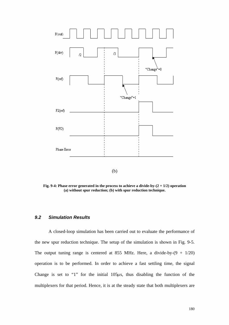
180
(b)
Fig. 9-4: Phase error generated in the process to achieve a divide-by-(2 + 1/2) operation (a) without spur reduction; (b) with spur reduction technique.
9.2 Simulation Results
A closed-loop simulation has been carried out to evaluate the performance of
the new spur reduction technique. The setup of the simulation is shown in Fig. 9-5.
The output tuning range is centered at 855 MHz. Here, a divide-by-(9 + 1/20)
operation is to be performed. In order to achieve a fast settling time, the signal
Change is set to “1” for the initial 105µs, thus disabling the function of the
multiplexers for that period. Hence, it is at the steady state that both multiplexers are
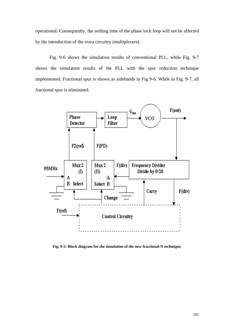
181
operational. Consequently, the settling time of the phase lock loop will not be affected
by the introduction of the extra circuitry (multiplexers).
Fig. 9-6 shows the simulation results of conventional PLL, while Fig. 9-7
shows the simulation results of the PLL with the spur reduction technique
implemented. Fractional spur is shown as sidebands in Fig 9-6. While in Fig. 9-7, all
fractional spur is eliminated.
Fig. 9-5: Block diagram for the simulation of the new fractional-N technique.

182
Fig. 9-6: Simulation results of a conventional fractional-N PLL.
Fig. 9-7: Simulation results of the new fractional-N PLL with spur reduction circuit implemented.
Frequency (MHz)
F(ou
t) in
dB
m
m1 freq=859.3 MHz dB(VCO)=-6.436
No fractional spur
F(ou
t) in
dB
m
Frequency (MHz)
m2 freq=854.5MHz dB(VCO)=-62.988
m1 freq=859.3MHz dB(VCO)=-6.838
Fractional spur

183
9.3 Summary
A new spur reduction frequency divider has been proposed. The advantage of
this technique besides its ability to eliminate all fractional spur is its simplicity
requiring only two extra 2-to-1 multiplexers. The simulation was performed using the
CSM 0.25µm technology, and the HP Advanced Design System. The work was
published in [109].
184
CHAPTER 10
Conclusions & Recommendations
10.1 Conclusions
This thesis describes a wide range of techniques employed in phase-locked
loop. The investigation covers mainly two building blocks of the phase-locked loop,
which are the VCO and the frequency divider.
In Chapter 2, the importance of optimizing the loop bandwidth in order to
achieve the best phase noise performance for a phase-locked loop was shown. The
impact of the noise generated from the resistor in the loop filter was highlighted. In
Chapter 3, an overview of the VCO design was presented, and the design
considerations for an LC VCO were shown. In Chapter 4, a novel parasitic-
compensated quadrature LC oscillator was presented.
A fabricated 2.63 GHz quadrature CMOS LC oscillator with a phase noise of
–112.3 dBc/Hz at 600 kHz offset was demonstrated, with a power consumption of
7.5mW at 1.5V supply using an on-chip spiral inductor.
A novel RF CMOS low-phase-noise LC oscillator using the memory reduction
tail transistor was presented in Chapter 5. A simulated phase noise of -127.6 dBc/Hz
at 600 kHz offset for an oscillation frequency of 1.88 GHz was achieved with a tank
quality factor of 9. An example of a VCO that meets the system specifications of the
WCDMA/CDMA2000 has been achieved through this novel topology. In Chapter 6,
the design of the novel 102 GHz SiGe MOSFETs LC oscillator was presented. The
VCO has an oscillation frequency of 102 GHz with a tuning range of 3.4 GHz. In this
185
tuning range, the phase noise was –106 dBc/Hz to –107.7 dBc/Hz at 1 MHz offset
frequency. Besides being the VCO with the highest frequency reported to date, this
novel VCO also has the best figure of merit (FOM) of 192.9 dB.
In Chapter 7, a literature review of the frequency dividers was given and a
design method was outlined for the implementation of high speed flip-flop, the basic
building block of frequency dividers. In Chapter 8, the design of a novel fully
integrated CMOS fractional-N frequency divider for wide-band mobile applications
with spur reduction technique was described. The frequency divider was fabricated
and experimentally verified. A novel spur reduction fractional-N frequency divider
was proposed in Chapter 9. Simulation results showed that the fractional spur was
fully suppressed with the implementation of this technique.
On-wafer measurements of the above circuits were carried out using the
HP8510C Network Analyzer (as shown in Fig. 10-1) and Cascade Microtech
Coplanar Ground-Signal Ground (GSG) probes. The HP Spectrum Analyzer 8593E
with the frequency range from 9 kHz to 26.5 GHz was connected to the RF probe to
examine the spectrums of the VCO output.
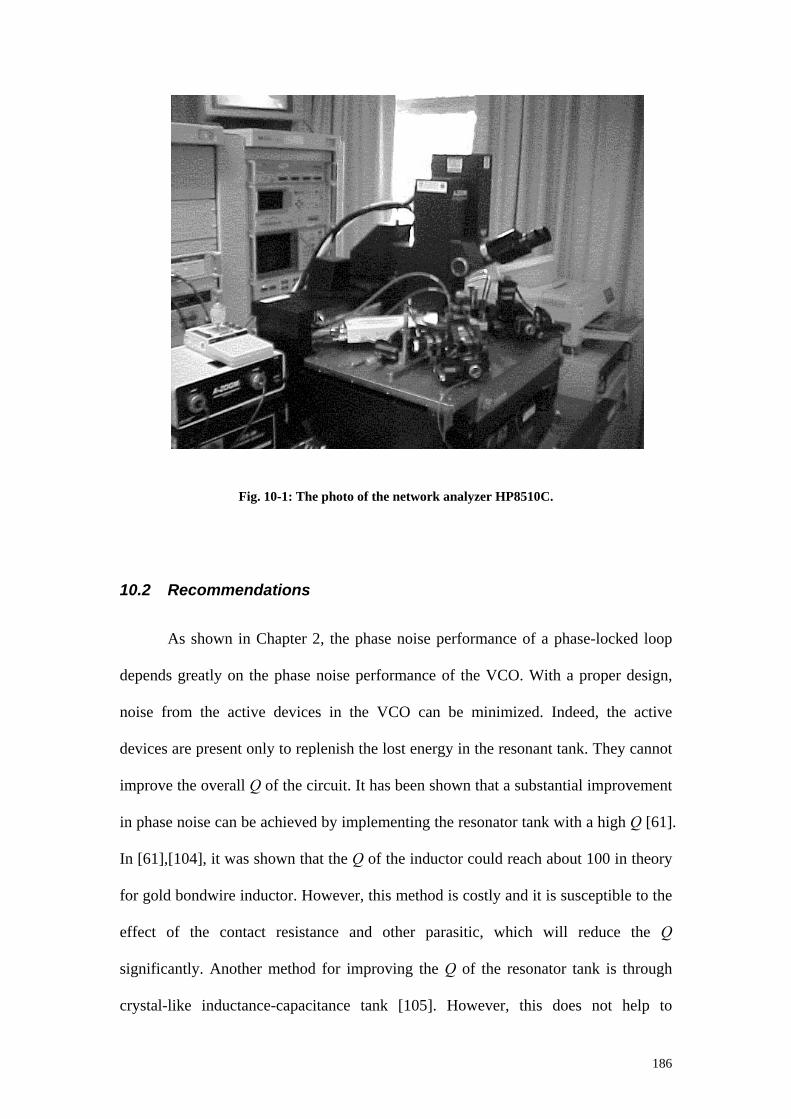
186
Fig. 10-1: The photo of the network analyzer HP8510C.
10.2 Recommendations
As shown in Chapter 2, the phase noise performance of a phase-locked loop
depends greatly on the phase noise performance of the VCO. With a proper design,
noise from the active devices in the VCO can be minimized. Indeed, the active
devices are present only to replenish the lost energy in the resonant tank. They cannot
improve the overall Q of the circuit. It has been shown that a substantial improvement
in phase noise can be achieved by implementing the resonator tank with a high Q [61].
In [61],[104], it was shown that the Q of the inductor could reach about 100 in theory
for gold bondwire inductor. However, this method is costly and it is susceptible to the
effect of the contact resistance and other parasitic, which will reduce the Q
significantly. Another method for improving the Q of the resonator tank is through
crystal-like inductance-capacitance tank [105]. However, this does not help to
187
improve the Q due to the requirement that all the inductors must be integrated on-chip.
More work has to be done in order to provide a resonator tank with high Q that can be
easily integrated.
The frequency divider is a critical block in a phase-locked loop frequency
synthesizer as well as in a clock and data recovery circuitry. One of the most
challenging requirements for a frequency divider is its speed of operation. The D-flip-
flop (FF) is commonly used as a frequency divider due to its high speed [116]-[118].
To date, some of the high speed FFs that have been developed, e.g., 40 Gb/s delayed
flip-flop (D-FF) with GaAs HBT [116], 25 Gb/s D-FF with Silicon bipolar [117],
24 Gb/s Super-Dynamic FF with GaAs MESFET [115], and 13.4 GHz Master-Slave
FF with MOSFET [1]. A conventional Master-Slave D-FF can operate at the speed of
one-fifth to one-fourth of the transistor ft for FET devices and one-fourth to one-third
of the transistor fmax for bipolar devices [118],[119]. For high speed applications, e.g.,
the 40 Gb/s Optical Communication – 768 (OC-768) standards, transistors with an ft
of 200 GHz are needed for a frequency divider circuit employing FET devices. Hence,
circuit innovations are urgently needed to make further speed improvements. This
presents a challenge to an RFIC circuit designer.
188
Author’s Publications
C. C. Boon, M. A. Do, K. S. Yeo, J. G. Ma, and R. Y. Zhao, “Parasitic-
Compensated Quadrature LC Oscillator”, IEE Proceedings : Circuits, Devices &
Systems, Vol. 151, No. 1, Feb. 2004.
C. C. Boon, M. A. Do, K. S. Yeo, J. G. Ma, and X. L. Zhang, “RF CMOS
Low-Phase-Noise LC Oscillator Through Memory Reduction Tail Transistor IEEE
Transaction On Circuits and Systems- II: Express Briefs, Analog and Digital Signal
Processing, Vol. 51, No. 2, Feb. 2004.
C. C. Boon, M. A. Do, K. S. Yeo, and J. G. Ma, “A Spur Reduction
Fractional-N Frequency Divider”, Microwave and Optical Technology Letter, Wiley
Interscience, vol. 33, no. 5, Apr. 2002.
C. C. Boon, M. A. Do, K. S. Yeo, and J. G. Ma, “Fully Integrated CMOS
Fractional-N Frequency Divider for Wide-Band Mobile Applications with Spurs
Reduction”, submitted to IEEE Transaction on Circuits and Systems- I, Dec. 2003.
C. C. Boon, M. A. Do, K. S. Yeo, and J. G. Ma, “102 GHz SiGe MOSFETs
LC Oscillator”, submitted to IEEE Transaction on Circuits and Systems- I, Jan. 2004.
C. C. Boon, M. A. Do, K. S. Yeo, and J. G. Ma, “A New Spur Reduction
Fractional-N Frequency Divider”, Proceedings IEEE International Symposium on
Integrated Circuit, Devices & System, 2001.
C. C. Boon, M. A. Do, K. S. Yeo, and J. G. Ma, “Multiple Modulus N+1/2
Fractional-N Frequency Divider”, Proceedings European Microwave Week, 2001.
189
Bibliography
[1] B. Razavi, K. F. Lee, and R. H. Yan, “Design of High-Speed, Low-Power
Frequency Dividers and Phase-Locked Loops in Deep Submicron CMOS”, IEEE
Journal of Solid-State Circuits, vol. 30, no. 2, pp. 101-109, Feb. 1995.
[2] E. A. Sovero, A. Hendarman, B. Massey, C. Wu, R. McDonough, N.
Hendrickson, A. Huelsman, and I. Deyhimy, “Recent Progress in 40Gb/s IC/OEIC
Design and Manufacturing”, Laser and Electro-Optic Society, LEOS 2001, vol. 2,
pp. 501-502, 2001.
[3] G. Gillette, “The Digiphase Synthesizer”, Proceedings of 23rd Annual Frequency
Control Symposium, 1969.
[4] J. Gibbs and R. Temple, “Frequency Domain Yields Its Data to Phase-Locked
Synthesizer”, Electronics, pp.107-113, Apr. 1978.
[5] D. G. Wilson, W. Rhee, and B. S. Song, “Low Power RF Receiver Front Ends and
Frequency Synthesizers for Wireless”, IEEE ISCAS, Tutorial Workshop, 1996.
[6] V. Manassewitsch, “Frequency Synthesizers – Theory and Design”, Wiley-
Interscience, pp. 283-284, 1987.
[7] Y. Koo, H. Huh, Y. Cho, J. Lee, J. Park, K. Lee, D-K. Jeong, and W. Kim, “A
Fully Integrated CMOS Frequency Synthesizer With Charge-Averaging Charge
Pump and Dual-Path Loop Filter for PCS- and Cellular-CDMA Wireless
Systems”, IEEE Journal of Solid-State Circuits, vol. 37, no. 5, pp. 536-542, May
2002.
[8] J. Zhou, M. Cheng, and L. Forbes, “SPICE Models for Flicker Noise in p-
MOSFETs in the Saturation Region”, IEEE Transactions on Computer-Aided
Design of Integrated Circuits and System, vol. 20, no. 6, pp. 763-767, Jun. 2001.
[9] F. N. Hoogee, “1/f Noise”, Physica, vol. 83B, pp. 14-23, 1976.
190
[10] F. Svelto and R. Castello, “A Bond-Wire Inductor-MOS Varactor VCO Tunable
From 1.8 to 2.4 GHz”, IEEE Transaction on Microwave Theory and Techniques,
vol. 50, no. 1, pp. 403-407, Jan. 2002.
[11] C. M. Hung and K. O. Kenneth, “A Packaged 1.1-GHz CMOS VCO with Phase
Noise of –126 dBc/Hz at a 600-kHz Offset”, IEEE Journal of Solid-State Circuits,
vol. 35, no. 1, pp. 100-103, Jan. 2000.
[12] S. Levantino, C. Samori, A. Bonfanti, S. L. J. Gierkink, A. L. Lacaita, and V.
Bocuzzi, “Frequency Dependence on Bias Current in 5-GHz CMOS VCOs:
Impact on Tuning Range and Flicker Noise Upconversion”, IEEE Journal of
Solid-State Circuits, vol. 37, no. 8, pp. 1003-1011, Aug. 2002.
[13] J. C. Chang, A. A. Abidi, and C. R. Viswananthan, “Flicker Noise in CMOS
Transistors from Subthreshold to Strong Inversion at Various Temperatures”,
IEEE Trans. Electron Devices, vol. 41, pp. 1965-1971, Nov. 1994.
[14] A. Springer, L. Maruer, and R. Weigel, “RF System Concepts for Highly
Integrated RFICs for W-CDMA Mobile Radio Terminals”, IEEE Transactions on
Microwave Theory and Techniques, vol. 50, no. 1, pp. 254-267, Jan. 2002.
[15] J. C. Haartsen, “The Bluetooth Radio System”, IEEE Pers. Commun., vol. 7, pp.
28-36, Feb. 2000.
[16] R. Van Nee, G. Awater, M. Morikura, H. Takanashi, M. Webster, and K. W.
Halford, “New High-Rate Wireless LAN Standards”, IEEE Commun. Mag., vol.
37, Dec. 1999.
[17] H. Sari, “A State-of-the-Art-Review of Broadband Wireless Access”, Proceedings
Eur. Wireless Technology Conference, Paris, France, pp. 310-315, Oct. 2000.
[18] M. Wurzer, J. Bock, H. Knapp, W. Zirwas, F. Schumann, and A. Felder, “A
40-Gb/s Integrated Clock and Data Recover Circuit in 50-GHz fT Silicon Bipolar
191
Technology”, IEEE Journal of Solid-State Circuits, vol. 34, no. 9, pp. 1320-1324,
Sep. 1999.
[19] J. Craninckx and M. S. J. Steyaert, “A Fully Integrated CMOS DCS-1800
Frequency Synthesizer”, IEEE Journal of Solid-State Circuits, vol. 33, no. 12, pp.
2054-2065, Dec. 1998.
[20] B. Razavi, “Design of High-Speed Circuits for Optical Communication Systems”,
IEEE Custom Integrated Circuits Conference, Session 14-1, pp. 315-322, 2001.
[21] E. Drucker, “Model PLL Dynamics and Phase-Noise Performance”, Microwave &
RF, pp. 73-117, Feb. 2000.
[22] V. F. Kroupa, “Noise Properties of PLL Systems”, IEEE Trans. Comm., vol. 30,
no. 10, pp. 2244-2252, Oct. 1982.
[23] A. Hajimiri, “Noise in Phase-Locked Loops”, 2001 Southwest Symposium on
Mixed-Signal Design, pp. 1-6, 2001.
[24] E. J. Baghdady, R. N. Lincoln, and B. D. Nelin, “Short-Term Frequency Stability:
Characterization, Theory, and Measurement”, Proceedings of IEEE, vol. 53, pp.
704-722, Jul. 1965.
[25] L. S. Cutler and C. L. Searle, “Some Aspects of the Theory and Measurement of
Frequency Fluctuations in Frequency Standards”, Proceedings of IEEE, vol. 54,
pp. 136-154, Feb. 1966.
[26] D. B. Leeson, “A Simple Model of Feedback Oscillator Noise Spectrum”,
Proceedings of IEEE, vol. 54, pp. 136-154, Feb. 1966.
[27] C. Barrett, “Fractional/Integer-N PLL Basics”, Texas Instruments Technical Brief
SWRA029, Aug. 1999.
[28] J. Craninckx and M. Steyaert, “Wireless CMOS Frequency Synthesizer Design”,
1st Edition, Boston Kluwer Academic Publishers, 1998.
192
[29] W. F. Egan, “Frequency Synthesis by Phase Lock”, New York Wiley & Sons,
1981.
[30] F. M. Gardner, “Phaselock Techniques”, 2nd Edition, New York Wiley & Sons,
1979.
[31] R. E. Best, “Phase-Locked Loops: Theory and Applications”, New York CRC
Press, 1997.
[32] F. M. Gardner, “Charge-Pump Phase Locked Loops,” IEEE Trans. Comm., vol.
28, pp. 1849-1859, Nov. 1980.
[33] D. H. Wolaver, “Phase-Locked Loop Circuit Design”, New Jersey Prentice Hall,
1991.
[34] M. Souyuer and R. G. Meyer, “Frequency Limitation of a Conventional Phase-
Frequency Dectector”, IEEE Journal Of Solid-State Circuits, vol. 25, no. 4, pp.
1019-1022, Aug. 1990.
[35] A. Hill and J. Surber, “The PLL Dead Zone and How to Avoid It”, RF Design, pp.
131-134, Mar. 1992.
[36] D. Mijuskovic, M. J. Bayer, T. F. Chomicz, N. K. Garg, F. James, P. W.
McEntarfer, and J. A. Porter, “Cell Based Fully Integrated CMOS Frequency
Synthesizers”, IEEE Journal of Solid-State Circuits, vol. 29, no. 3, pp. 271-279,
Mar. 1994.
[37] W. O. Keese, “An Analysis and Performance Evaluation of a Passive Filter
Design Technique for Charge Pump PLLs”, National Semiconductor Application
Note AN012473, 1996.
[38] H. Meyr and G. Ascheid, “Synchronization in Digital Communication, Vol. 1:
Phase-, Frequency Locked Loops and Amplitude Control”, New York Wiley &
Sons, 1990.
193
[39] P. Hugues, “UMA1021M Low Voltage Frequency Synthesizer”, Philips
Semiconductors Application Note AN96083, 1996.
[40] P. R. Gray and R. G. Meyer, “Analysis and Design of Analog Integrated Circuits”,
2nd Edition, New York Wiley, 1984.
[41] D. L. Chen and R. Waldorn, “A Single-Chip 266-Mb/s CMOS
Transmitter/Receiver for Serial Data Communications”, ISSCC Digest of
Technical Papers, San Fransisco, pp. 100-101, Feb. 1993.
[42] M. Banu and A. Dunlop, “A 660-Mb/s CMOS Clock Recover Circuits with
Instantaneous Locking for NRZ Data and Burst-Mode Transmission”, ISSCC
Digest of Technical Papers, San Fransisco, pp. 102-103, Feb. 1993.
[43] A. Pottbacker and U. Langmann, “An 8-GHz Silicon Bipolar Clock Recovery and
Data-Generator IC”, IEEE Journal of Solid-State Circuits, vol. 29, no. 12, pp.
1572-1578, Dec. 1994.
[44] B. Razavi and J. Sung, “A 6-GHz 60-mW BiCMOS Phase Locked Loop with 2-V
Supply”, ISSCC Digest of Technical Papers, San Fransisco, pp. 114-115, Feb.
1994.
[45] S. T. Yan and H. C. Luong, “A 3V 1.3-to-1.8 GHz CMOS Voltage-Controlled
Oscillator with 0.3 ps-Jitter”, 1997 IEEE International Symposium on Circuits and
Systems, Hong Kong, pp. 29-32, Jun. 1997.
[46] Z. M. Lin and C. H. Huang, “A Current-Source Driven CMOS Voltage-Controlled
Oscillator”, Proceedings of ICECS '99. The 6th IEEE International Conference on
Electronics, Circuits and Systems, vol. 3, pp.1337-1339, Sep. 1999.
[47] W. Rhee, “A Low Power, Wide Linear-Range CMOS Voltage-Controlled
Oscillator”, ISCAS '98. Proceedings of the 1998 IEEE International Symposium
on Circuits and Systems, vol. 2, pp.85-88, 1998.

194
[48] H. Chen, E. Lee, and R. Geiger, “A 2 GHz VCO with Process and Temperature
Compensation”, Proceedings of the 1999 IEEE International Symposium on
Circuits and Systems, ISCAS 1999, vol. 2, pp.569-572, 1999.
[49] B. Razavi, “Design of Analog CMOS Integrated Circuits”, McGraw-Hill
International Edition Electrical Engineering Series, 2000.
[50] B. Razavi, “A Study of Phase Noise in CMOS Oscillators”, IEEE Journal of
Solid-State Circuits, vol. 31, no. 3, pp. 331-343, Mar. 1996.
[51] M. Thamsirianunt and T. Kwasniewski, “CMOS VCOs for PLL Frequency
Synthesis in GHz Digital Mobile Radio Communications”, Proceedings of the
IEEE CICC, pp. 331-334, May 1995.
[52] B. Razavi, “RF Microelectronic”, Prentice Hall, 1998.
[53] M. Tiebout, “Low Power Low-Phase-Noise Differentially Tuned Quadrature VCO
Design in Standard CMOS”, IEEE Journal of Solid-State Circuits, vol. 36, no. 7,
pp. 1018-1024, Jul. 2001.
[54] B. Razavi, “A 1.8-GHz CMOS Voltage-Controlled Oscillator”, ISSCC Digest of
Technical Papers, San Fransisco, pp. 388-389, Feb. 1997.
[55] T. H. Lee, “The Design of CMOS Radio-Frequency Integrated Circuits”,
Cambridge University Press, 1998.
[56] J. Crols, P. Kinget, J. Craninckx, and M. Steyaert, “An Analytical Model of Planar
Inductors on Lowly Doped Silicon Substrates for High Frequency Analog Design
up to 3GHz”, 1996 Symposium on VLSI Circuits Digest of Technical Papers, pp.
28-29, 1996.
[57] J. Craninckx and M. Steyaert, “A 1.8-GHz Low-Phase-Noise CMOS VCO Using
Optimized Hollow Spiral Inductors”, IEEE Journal of Solid-State Circuits, vol.
32, pp.736-744, May 1997.

195
[58] E. Hegazi, H. Sjoland, and A. A. Abidi, “A Filtering Technique to Lower LC
Oscillator Phase Noise”, IEEE Journal of Solid-State Circuits, vol. 36, no. 12, pp.
1921-1930, Dec. 2001.
[59] A. Hajimiri and T. H. Lee, “Design Issues in CMOS Differential LC Oscillators”,
IEEE Journal of Solid-State Circuits, vol. 34, pp. 717-724, May 1999.
[60] F. Herzel, M. Pierschel, P. Weger, and M. Tiebout, “Phase Noise in Differential
CMOS Voltage-Controlled Oscillator for RF Applications”, IEEE Trans. On
Circuits and System-II: Analog and Digital Signal Processing, vol. 47, no. 1, pp.
11-15, Jan. 2000.
[61] P. Vancorenland and M. S. J. Steyaert, “A 1.57-GHz Fully Integrated Very Low-
Phase-Noise Quadrature VCO”, IEEE Journal of Solid-State Circuits, vol. 37, no.
5, May 2002.
[62] B. Razavi, “A 5.2-GHz CMOS Receiver with 62-dB Image Rejection”, IEEE
Journal of Solid-State Circuits, vol. 36, no. 5, pp. 402-403, May 2001.
[63] A. Rofougaran, G. Chang, J. J. Rael, J. Y. C. Chang, M. Rofougaran, P. J. Chang,
M. Djafari, J. Min, E. Roth, A. A. Abidi, and H. Samueli, “A Single-Chip 900-
MHz Spread-Spectrum Wireless Transceiver in 1-µm CMOS-Part I: Architecture
and Transmitter Design”, IEEE Journal of Solid-State Circuits, vol. 33, no. 4, pp.
515-534, Apr. 1998.
[64] A. Rofougaran, “A 900MHz CMOS LC Oscillator with Quadrature Outputs”,
ISSCC Digest of Technical Papers, pp.392-393, Feb.1996.
[65] C. Lam and B. Razavi, “A 2.6GHz/5.2GHz CMOS Voltage-Controlled
Oscillator”, ISSCC Digest of Technical Papers, pp.402-403, Feb. 1999.

196
[66] T. P. Liu, “A 6.5GHz Monolithic CMOS Voltage-Controlled Oscillator”, ISSCC
Digest of Technical Papers, pp.404-405, Feb.1999.
[67] P. Andreani and S. Mattisson, “On the Use of MOS Varactors in RF VCO’s”,
IEEE Journal of Solid-State Circuits, vol. 35, no. 6, pp. 905-910, Jun. 2000.
[68] C. Samori, A. L. Lacaita, A. Zanchi, S. Levantino, and F. Torrisi, “Impact of
Indirect Stability on Phase Noise Performance of Fully-Integrated LC Tuned
VCOs”, Proceedings of ESSCIRC 1999, pp. 202-205, Sep. 1999.
[69] J. W. M. Rogers, J. A. Macedo, and C. Plett, “The effect of Varactor Nonlinearity
on the Phase Noise of Completely Integrated VCOs”, IEEE Journal of Solid-State
Circuits, vol. 35, no. 9, pp. 1360-1367, Sep. 2000.
[70] J. J. Kim and B. Kim, “A Low-Phase Noise CMOS LC Oscillator with a Ring
Structure”, IEEE ISSCC Digest of Technical Papers, pp. 430-431, Feb. 2000.
[71] A. M. ElSayed and M. I. Elmasry, “Low-Phase-Noise LC Quadrature VCO Using
Coupled Tank Resonators in a Ring Structure”, IEEE Journal of Solid-State
Circuits, vol. 36, no. 4, pp. 701-705, Apr. 2001.
[72] T. P. Liu, “1.5V 10-12.5 GHz Integrated CMOS Oscillators”, Symposium on VLSI
Digest of Technical Papers, pp. 55-56, 1999.
[73] J. van der Tang, P. van de Ven, D. Kasperkovitz, and A. van Roermund, “Analysis
and Design of an Optimally Coupled 5-GHz Quadrature LC Oscillator”, IEEE
Journal of Solid-State Circuits, vol. 37, no. 5, pp. 657-661, May 2002.
[74] A. S. Porret, T. Melly, and C. C. Enz, “Design of High-Q Varactors for Low-
Power Wireless Applications Using a Standard CMOS Process”, Proceedings of
CICC ’99, pp. 641-644, May 1999.

197
[75] M. D. M. Hershenson, A. Hajimiri, S. S. Mohan, S. P. Boyd, and T. H. Lee,
“Design and Optimization of LC Oscillators”, IEEE/ACM Conference on
Computer-Aided, Design Digest of Technical Paper, pp. 65-69, 1999.
[76] D. A. Johns and K. Martin, “Analog Integrated Circuit Design”, John Wiley &
Sons, 1997.
[77] D. Ham and A. Hajimiri, “Concepts and Methods in Optimization of Integrated
LC VCOs”, IEEE Journal of Solid-State Circuits, vol. 36, no. 6, pp. 896-909, Jun.
2001.
[78] L. E. Frenzel, “Transceiver Chip Set Wrings Out CSM Phone Costs”, Electron.
Design, pp. 78-82, Mar. 2001.
[79] P. Andreani and H. Sjoland, “Tail Current Noise Suppression in RF CMOS
VCOs”, IEEE Journal of Solid-State Circuits, vol. 37, no. 3, pp. 342-348, Mar.
2002.
[80] C. Samori, A. L. Lacaita, F. Villa, and F. Zappa, “Spectrum Folding and Phase
Noise in LC Tuned Oscillators”, IEEE Transactions on Circuits and Systems – II,
vol. 45, pp. 781-790, Jul. 1998.
[81] C. Samori, S. Levantino, and V. Boccuzzi, “A –94dBc/Hz@100KHz, Fully-
Integrated, 5-GHz, CMOS VCO with 18% Tuning Range for Bluetooth
Applications”, Proceedings of CICC 2001, pp. 201-204, May 2001.
[82] S. Kogan, “Electronic Noise and Fluctuations in Solids”, Cambridge, U.K.:
Cambridge University Press, 1996.
[83] K. K. Hung, P. K. Ko, C. Hu, and Y. C. Cheng, “A Unified Model for Flicker
Noise in Metal-Oxide-Semiconductor Field-Effect Transistors”, IEEE Trans.
Electron Devices, vol. 37, pp. 654-665, Mar. 1990.

198
[84] E. A. M. Klumperink, S. L. J. Gierkink, A. P. van der Wel, and B. Nauta,
“Reducing MOSFET 1/f Noise and Power Consumption by Switch Biasing”,
IEEE Journal of Solid-State Circuits, vol. 35, no. 7, pp. 994-1001, Jul. 2000.
[85] S. L. J. Gierkink, E. A. M. Klumperink, A. P. van der Wel, G. Hoogzaad, E. van
Tuijl, and B. Nauta, “Intrinsic 1/f Device Noise Reduction and Its Effect on Phase
Noise in CMOS Ring Oscillators”, IEEE Journal of Solid-State Circuits, vol. 34,
no. 7, pp. 1022-1025, Jul. 1999.
[86] J. J. Rael and A. A. Abidi, “Physical Processes of Phase Noise in Differential LC
Oscillators”, Proceedings of CICC 2000, pp. 569-572, 2000.
[87] H. Ronkainen, H. Kattelus, E. Tarvainen, T. Riihisaari, M. Andersson, and P.
Kuivalainen, “IC Compatible Planar Inductors in Silicon”, IEE Proceedings on
Circuits, Devices and Systems, pp. 25-29, Feb. 1997.
[88] H. M. Wang, “A 50GHz VCO in 0.25 µ m CMOS”, Digest of Technical Papers
ISSCC, pp. 372-373, 2001.
[89] H. Li, H. M. Rein, R. Kreienkamp, and W. Klein, “47 GHz VCO With Low Phase
Noise Fabricated in a SiGe Bipolar Production Technology”, IEEE Microwave
and Wireless Components Letters, vol. 12, no. 3, pp. 79-81, Mar. 2001.
[90] M. Tiebout, H. D. Wohlmuth, and W. Simburger, “A 1V 51GHz Fully-Integrated
VCO in 0.12 µ m CMOS”, Digest of Technical Paper ISSCC, pp. 467-469, 2002.
[91] J. Yuan and C. Svensson, “High-Speed CMOS Circuit Technique”, IEEE Journal
of Solid-State Circuits, vol. 24, no.1, pp.62-70, Feb. 1989.
[92] Q. T. Huang, “Speed Optimization of Edge-Triggered CMOS Circuits for
Gigahertz Single-Phase Clocks”, IEEE Journal of Solid-State Circuits, vol. 31, no.
3, pp. 456-465, Mar. 1996.

199
[93] C. Y. Yang, G. K. Dehng, J. M. Hsu, and S. L. Liu, “New Dynamic Flip-Flops for
High-Speed Dual-Modulus Prescaler”, IEEE Journal of Solid-State Circuits, vol.
33, no. 10, pp. 1568-1571, Oct. 1998.
[94] J. Craninckx and M. S. J. Steyaert, “A 1.75GHz/3V Dual Modulus Divide-by-
128/129 Prescaler in 0.7µm CMOS,” IEEE Journal of Solid-State Circuits, vol.
31, no. 7, pp. 890-897, Jul. 1996.
[95] -, “Dana Series 7000 Digiphase Frequency Synthesizers,” Publication 980428
(Manual), Dana Laboratories, Inc.
[96] V. Reinhardt and I. Shahriary, “Spurless Fractional Divider Direct Digital
Synthesizer and Method”, U.S. Patent 4815018, Mar. 21, 1989.
[97] B. Miller, et al., “A Multiple Modulation Fractional Divider”, Proceedings of 44th
Annual Frequency Control Symposium, pp. 559-568, 1990.
[98] T. A. D. Riley, M. A. Copeland, and T. A. Kwasniewski, “Delta-Sigma
Modulation in Fractional-N Frequency Synthesis”, IEEE Journal of Solid-State
Circuits, vol. 28, pp. 553-559, May 1993.
[99] T. Nakagawa and T. Ohira, “A Phase Noise Reduction Technique for MMIC
Frequency Synthesizers that Uses a New Pulse Generator LSI”, IEEE Trans. On
Microwave Theory and Technique, vol. 42, no. 12, pp. 2579-2582, Dec. 1994.
[100] S. Obote, Y. Sumi, K. Tsuda, K. Syoubu, and Y. Fukui, “Novel Fractional-N PLL
Frequency Synthesizer with Reduced Phase Error”, Proceedings of IEEE Asia
Pacific Conference on Circuits and Systems, pp. 45-48, Nov. 1996.
[101] T. P. Liu and E. Westerwick, “5-GHz CMOS Radio Transceiver Front-End
Chipset”, IEEE Journal of Solid-State Circuits, vol. 35, no. 12, pp. 701-705, Dec.
2000.

200
[102] M. S. J. Steyaert, J. Janssens, B. de Muer, M. Borremans, and N. Itoh, “A 2-V
CMOS Cellular Transceiver Front-End”, IEEE Journal of Solid-State Circuits,
vol. 35, no. 12, pp. 1895-1907, Dec. 2000.
[103] H. S. Kao and C. Y. Wu, “A Compact CMOS 2V Low-Power Direct-Conversion
Quadrature Modulator Merged with Quadrature Voltage-Controlled Oscillator and
RF Amplifier for 1.9 GHz RF Transmitter Applications”, IEEE ISCAS Circuits
and Systems 2000, Geneva, vol. 4, pp. 765-768, 2000.
[104] J. Craninckx and M. S. Steyaert, “A 1.8-GHz CMOS Low-Phase-Noise Voltage-
Controlled Oscillator with Prescaler”, IEEE Journal of Solid-State Circuits, vol.
30, no. 12, pp. 1474-1482, Dec. 1995.
[105] A. L. Lacaita and C. Samori, “Phase Noise Performance of Crystal-Like LC
Tanks”, IEEE Transactions on Circuits and Systems –II: Analog and Digital
Signal Processing, vol. 45, no. 7, pp. 898-900, Jul. 1998.
[106] M. A. Do, R. Y. Zhao, K. S. Yeo, and J. G. Ma, “New Wideband/Dualband
CMOS LC Voltage-Controlled Oscillator”, IEE Proceedings Circuits Devices
Syst., In Press.
[107] C. C. Boon, M. A. Do, K. S. Yeo, J. G. Ma, and R. Y. Zhao, “Parasitic-
Compensated Quadrature LC Oscillator”, IEE Proceedings : Circuits, Devices &
Systems, Vol. 151, No. 1, Feb. 2004.
[108] C. C. Boon, M. A. Do, K. S. Yeo, J. G. Ma, and X. L. Zhang, “RF CMOS Low-
Phase-Noise LC Oscillator Through Memory Reduction Tail Transistor IEEE
Transaction On Circuits and Systems- II: Express Briefs, Analog and Digital
Signal Processing, Vol. 51, No. 2, Feb. 2004.

201
[109] C. C. Boon, M. A. Do, K. S. Yeo, and J. G. Ma, “A Spur Reduction Fractional-N
Frequency Divider”, Microwave and Optical Technology Letter, Wiley
Interscience, vol. 33, no. 5, Apr. 2002.
[110] D. W. Dobberpuhl, R. T. Witek, R. Allmon, R. Anglin, D. Bertucci, S. Britton, L.
Chao, R. A. Conrad, D. E. Dever, B. Gieseke, S. M. N. Hassoun, G. W. Hoeppner,
K. Kuchler, M. Ladd, B. M. Leary, L. Madden, E. J. McLellan, D. R. Meyer, and
J. Montanaro, “A 200-MHz 64-b Dual-Issue CMOS Microprocessor”, IEEE
Journal of Solid-State Circuits, vol. 27, no. 11, pp. 1555-1567, Nov. 1992.
[111] W. Rhee and A. Ali, “An On-Chip Phase Compensation Technique In Fractional-
N Frequency Synthesis”, IEEE ISCAS, vol. 3, pp. 363-366, Jun. 1999.
[112] A. S. Sedra and K. C. Smith, “Microelectronic Circuits”, Oxford University Press,
1998.
[113] Y. Tsividis, “Operation and Modeling of the MOS Transistor”, New York:
McGraw-Hill, 1987.
[114] C. C. Boon, M. A. Do, K. S. Yeo, and J. G. Ma, “Multiple Modulus N+1/2
Fractional-N Frequency Divider”, Proceedings of European Microwave Week,
2001.
[115] T. Otsuji, M. Yoneyama, K. Murata, and E. Sano, “A Super-Dynamic Flip-Flop
Circuit for Broad-Band Applications up to 24 Gb/s Utilizing Production-Level
0.2-µm GaAs MESFET’s”, IEEE Journal of Solid-State Circuits, vol. 32, no. 9,
pp. 1357-1362, Sep. 1997.
[116] Y. Kuriyama, T. Sugishita, S. Honjo, J. Akagi, K. Tsuda, N. Iizuka, and M. Obara,
“A 40 GHz D-Type Flip-Flop Using AlGaAs/GaAs HBT’s”, GaAs IC Symp.
Tech., pp. 182-192, Dec. 1994.

202
[117] A. Felder, R. Steng, J. Hauenschild, H. –M. Rein, and T. F. Meister, “25-40 Gb/s
Si IC’s in Selective Epitaxial Bipolar Technology”, IEEE Int. Solid-State Circuit
Conf. Tech. Dig., pp. 156-157, 1993.
[118] H. Ichino, M. Togashi, M. Ohhata, Y. Imai, N. Ishihara, and E. Sano, “Over 10-
Gb/s IC’s for Future Lightwave Communications”, IEEE J. Lightwave Technol.,
vol. 12, no. 2, pp. 308-319, 1994.
[119] E. Sano, Y. Matsuoka, and T. Ishibashi, “Device Figure-of-Merits for High Speed
Digital IC’s and Baseband Amplifiers”, IEICE Trans. Electron., vol. E78-C, no. 9,
pp. 1182-1188, 1995.
[120] U. L. Rohde, “Microwave and Wireless Synthesizers”, New York Wiley & Sons,
1997.