novel semiconductor alloys based on gasb for domestic pv
TRANSCRIPT
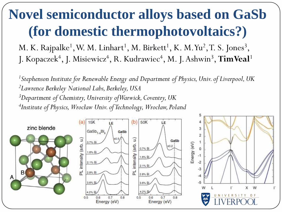
Novel semiconductor alloys based on GaSb
(for domestic thermophotovoltaics?)M. K. Rajpalke1, W. M. Linhart1, M. Birkett1, K. M. Yu2, T. S. Jones3,
J. Kopaczek4, J. Misiewicz4, R. Kudrawiec4, M. J. Ashwin3, TimVeal1
1Stephenson Institute for Renewable Energy and Department of Physics, Univ. of Liverpool, UK2Lawrence Berkeley National Labs, Berkeley, USA3Department of Chemistry, University of Warwick, Coventry, UK4Institute of Physics, Wrocław Univ. of Technology, Wrocław, Poland

Outline…
Summary of research on semiconductor materials for photovoltaics
Thermophotovoltaics
Molecular beam epitaxy of GaSb1-xBix alloys
Structural and compositional characterisation of GaSb1-xBix alloys
FT-IR absorption, photoreflectance and PL studies of GaSb1-xBix
alloys
Band structure of GaSb1-xBix alloys
Conclusions
2

Semiconductor materials for photovoltaics
3
Three main areas of research in progress:
Earth abundant semiconductors for sustainable TW scale solar PV
High mobility transparent conducting oxides
Semiconductors for improved efficiency thermophotovoltaics

4
Optical absorption spectroscopy of CuSbS2 thin films
DFT, Scanlon et al. (2012) Samples from Zaketayev et al., NREL
5
1020
1021
10
1005
1
7
43
2
Ele
ctr
on m
obili
ty (
cm
2V
-1s
-1)
Electron concentration (cm-3)
normal IIS
IIS with remote screening
In2O
3 undoped
In2O
3:Mo
In2O
3:Sn
1
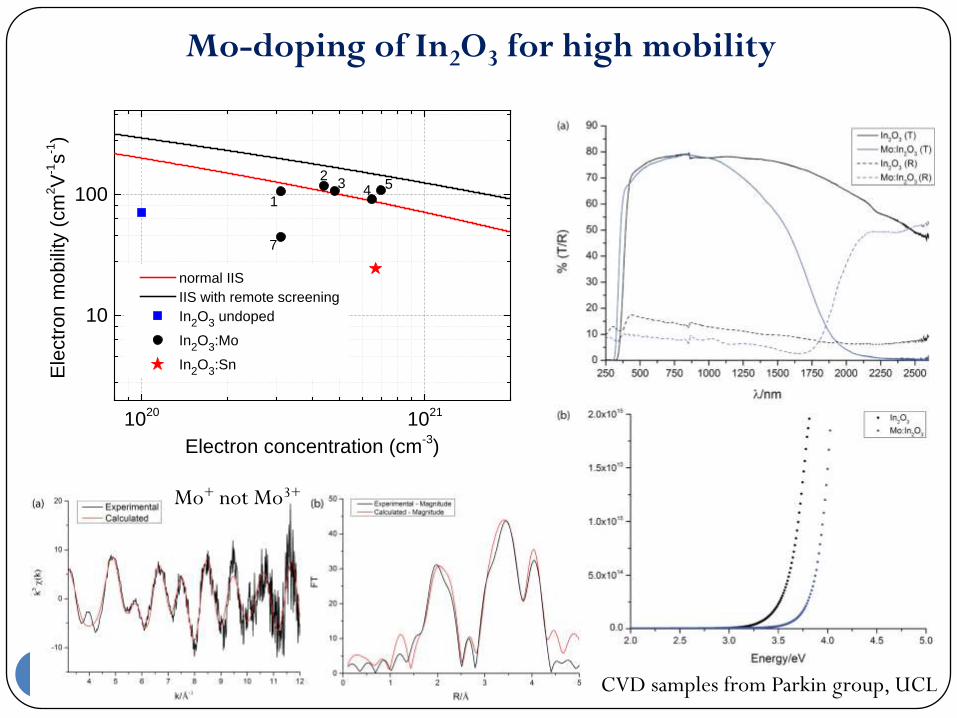
Mo-doping of In2O3 for high mobility
Mo+ not Mo3+
CVD samples from Parkin group, UCL
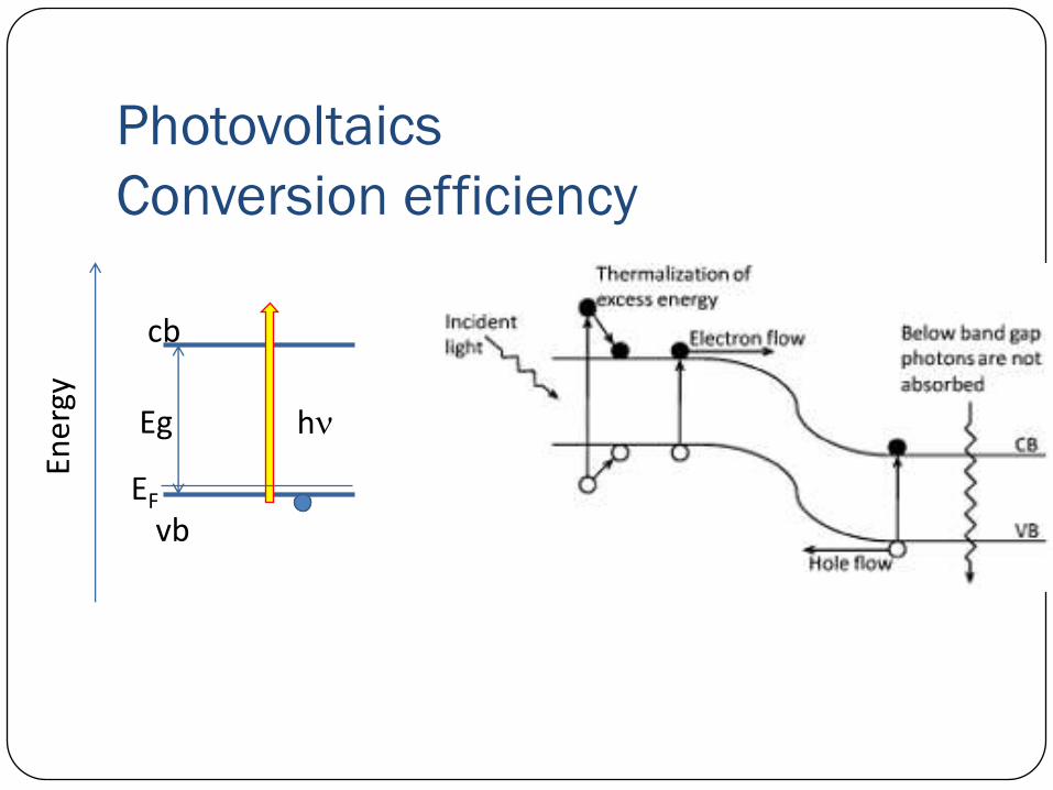
Photovoltaics
Conversion efficiency
Eg
cb
vbEF
hn
Ener
gy

Conversion efficiency
Eg
cb
vbEF
hn
p-type n-type
hn
One electron per photon Eg = energy available from each
K. Durose

Power at ground level is about 1000 W/m2

Thermophotovoltaics (TPV)
Solar photovoltaics can be seen as a special case of the more general thermophotovoltaics (TPV).
TPV systems consist of a heat source, an absorber/emitter material, a spectral filter and a
photovoltaic cell. In solar PV, the heat source is the sun!

Solar PV versus TPV
The Sun is about 1.5x10¹¹ m from the Earth.
So this is the emitter to PV cell distance in solar PV.
The incident power density from the Sun on Earth at ground
level is about 103 W/m2.
Power output from solar PV is about 150 W/m2
In TPV, the emitter is typically 10-1 m from the PV cell.
The incident power density onto PV cell can be 106 W/m2.
Power outputs can be higher than 104 W/m2.

TPV applications
TPV has no moving parts and is quiet. The applications of TPV and associated heat
sources are wide ranging and include:
(i) combined heat and power (CHP) generation from domestic boilers, so-called
micro-CHP, providing central heating and converting waste heat into
electricity;
(ii) CHP in remote (off-grid) locations to avoid the need for a separate generator;
(iii) hybrid cars, where the gas powered engine exhaust heat is converted by a TPV
device to charge the batteries which power the electric drive;
(iv) recovery of waste heat from nuclear power sources, especially for space
applications and submarines;
(v) military use to partly replace batteries or to charge them using logistic fuels;
and
(vi) recovery of waste energy from high temperature industries such as glass, steel
and cement.
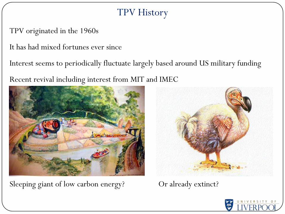
TPV History
TPV originated in the 1960s
It has had mixed fortunes ever since
Interest seems to periodically fluctuate largely based around US military funding
Recent revival including interest from MIT and IMEC
Sleeping giant of low carbon energy? Or already extinct?
13
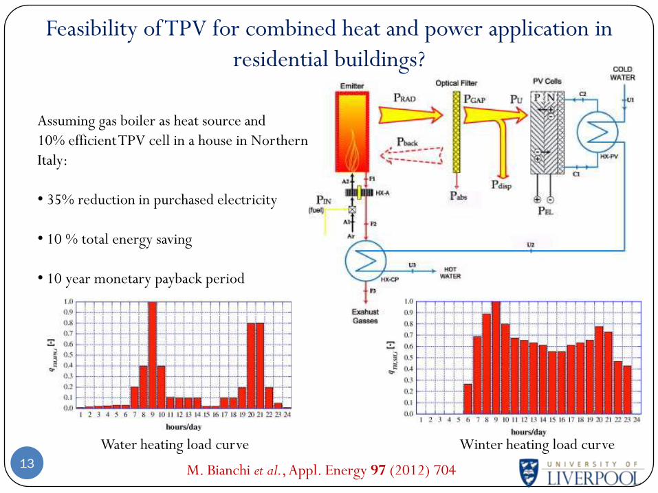
Feasibility of TPV for combined heat and power application in
residential buildings?
M. Bianchi et al., Appl. Energy 97 (2012) 704
Assuming gas boiler as heat source and
10% efficient TPV cell in a house in Northern
Italy:
• 35% reduction in purchased electricity
• 10 % total energy saving
• 10 year monetary payback period
Water heating load curve Winter heating load curve
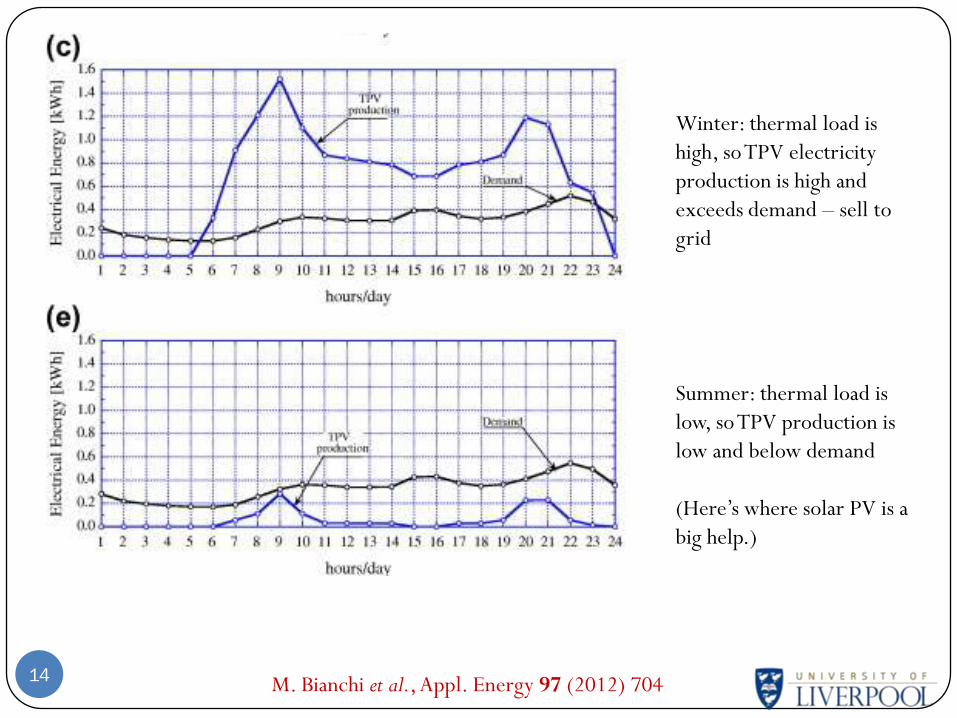
14
Winter: thermal load is
high, so TPV electricity
production is high and
exceeds demand – sell to
grid
Summer: thermal load is
low, so TPV production is
low and below demand
(Here’s where solar PV is a
big help.)
M. Bianchi et al., Appl. Energy 97 (2012) 704

Temperature dependence of black-body spectrum
Planck’s law
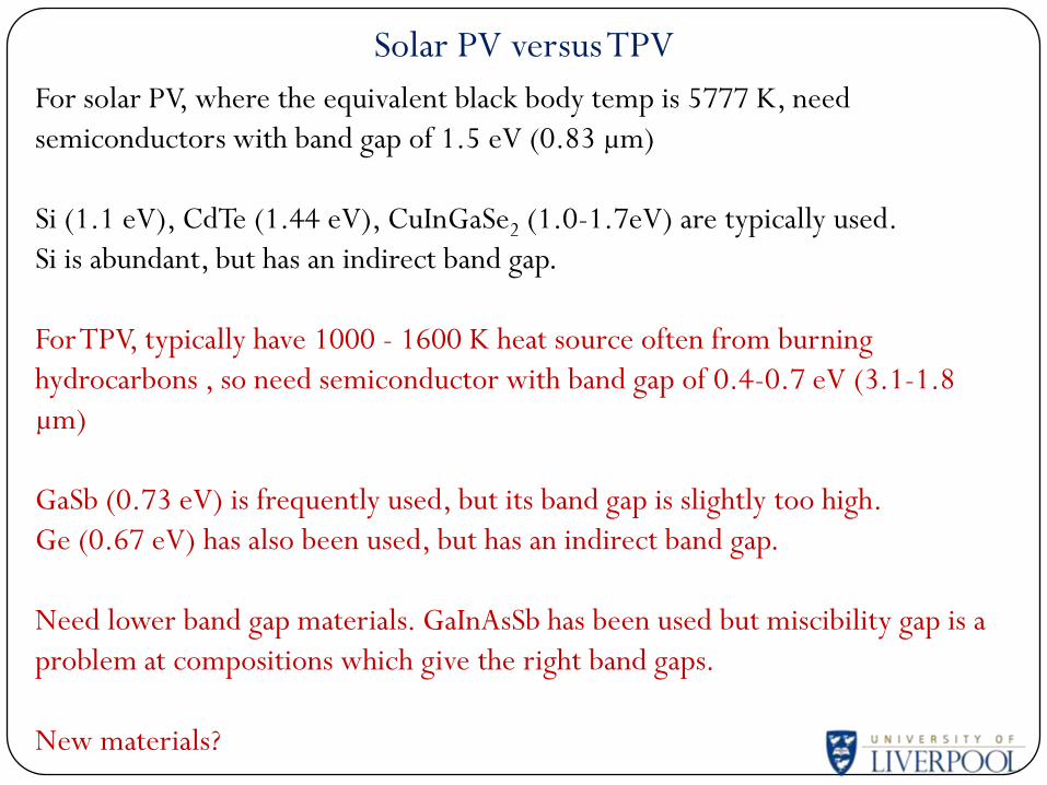
Solar PV versus TPV
For solar PV, where the equivalent black body temp is 5777 K, need
semiconductors with band gap of 1.5 eV (0.83 µm)
Si (1.1 eV), CdTe (1.44 eV), CuInGaSe2 (1.0-1.7eV) are typically used.
Si is abundant, but has an indirect band gap.
For TPV, typically have 1000 - 1600 K heat source often from burning
hydrocarbons , so need semiconductor with band gap of 0.4-0.7 eV (3.1-1.8
µm)
GaSb (0.73 eV) is frequently used, but its band gap is slightly too high.
Ge (0.67 eV) has also been used, but has an indirect band gap.
Need lower band gap materials. GaInAsSb has been used but miscibility gap is a
problem at compositions which give the right band gaps.
New materials?

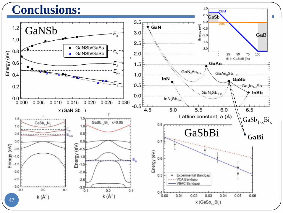
Introduction – dilute nitrides and GaNxSb1-x
17
Incorporation of a small amount of N atoms in III-V
semiconductors leads to a large band gap reduction.
This phenomenon is relatively
unstudied in antimonides.
Offers the possibility of tuning
the band gap with lattice matching
via the incorporation of In or Bi.
The properties of GaNxSb1-x
(and also Ga1-yInyNxSb1-x and
InNSb) have recently been determined.
18J. Wu et al., Semicond. Sci. Technol. 17 860 (2002)
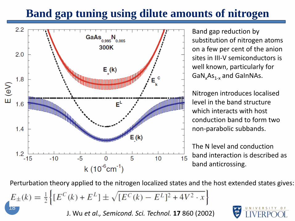
Band gap tuning using dilute amounts of nitrogen
Band gap reduction by substitution of nitrogen atoms on a few per cent of the anion sites in III-V semiconductors is well known, particularly for GaNxAs1-x and GaInNAs.
Nitrogen introduces localised level in the band structure which interacts with host conduction band to form two non-parabolic subbands.
The N level and conduction band interaction is described as band anticrossing.
Perturbation theory applied to the nitrogen localized states and the host extended states gives:

19
Band gap tuning using dilute amounts of nitrogen
The band anticrossinginteraction results in the lowest subband moving to lower energy as the amount of N is increased.
This enables the band gap to be tuned by controlling the amount of N.
Of course, the band gap of GaN is greater than that of GaAs, so initially adding N was expected to result in a larger band gap.
J. Wu et al., Semicond. Sci. Technol. 17 860 (2002)

Introduction – dilute nitrides and GaNxSb1-x
20
• Incorporation of a small amount of N atoms in III-V
semiconductors leads to a large band gap reduction.
• This phenomenon is relatively
unstudied in antimonides.
• Offers the possibility of tuning
the band gap with lattice matching
via the incorporation of In or Bi.
• The properties of GaNxSb1-x
(and also Ga1-yInyNxSb1-x and
InNSb) have recently been determined.
• However, GaNSb does not exhibit PL.

Introduction – dilute bismides and GaSb1-xBix
21
Incorporation of a small amount of Bi atoms in III-As semiconductors has been
shown to lead to a large band gap reduction, 84-90 meV/Bi%, in GaAsBi.
Gowth of InSbBi ternary alloys dates back to 1969
– it was the first “dilute bismide” alloy [eg. 1,2]
GaSb1-xBix grown by liquid phase epitaxy with
x < 0.01 [3]
Very few reports on growth of epitaxial GaSbBi
alloys [4,5]. Previous MBE material had lattice
contraction as Bi was added rather than expected
expansion.
Optical properties of GaSbBi are not yet established.
[1] J. L. Zilka. et.al. J. Appl. Phys. 51,1549 (1980).
[2] J. J. Lee.et.al. Appl. Phys. Lett. 70 , 3266 (1997)
[3] P. Gladkov.et.al. Journal of Crystal Growth 146 ,319 (1995)
[4] S.K. Das, et.al. Infrared Physics & Technology 55 (2012) 156
[5] Y.Song, et.al. J. Vac. Sci. Technol. B 30, 02B114 (2012)
C.A. Broderick, M.Usman,
S.J. Sweeney and E.P. O'Reilly,
Semicond. Sci. Technol. 27
094011 (2012)
GaAsBi

8-14 micron atmospheric transmission window
3-5 micron atmospheric transmission window
3-5 and 8-14 micron wavelengths are used for remote gas sensing, night vision, bio-medical imaging for diagnosis in healthcare and detection in optical spectroscopy.
Also 2-4 microns for thermophotovoltaics for waste heat recovery from glass and steel manufacturing and also from domestic heating systems.
Mid-infrared and long wavelength infrared applications
23
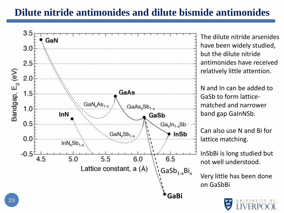
Dilute nitride antimonides and dilute bismide antimonides
GaBi
GaSb1-xBix
The dilute nitride arsenideshave been widely studied, but the dilute nitride antimonides have received relatively little attention.
N and In can be added to GaSb to form lattice-matched and narrower band gap GaInNSb.
Can also use N and Bi for lattice matching.
InSbBi is long studied but not well understood.
Very little has been done on GaSbBi

24
Conduction Band and Valence Band Anticrossing
Bi states located near the valence bands
anticrossing
N states located near the conduction
band anticrossing

25
Interaction between host and impurity p-like
states. Bi introduces 6 p-like localized states Interaction of localized N levels with
extended states of the conduction band.
Conduction Band and Valence Band Anticrossing

Molecular-Beam Epitaxy at Warwick
Gen II MBE system:
Group III cells: Al, Ga, In
Group V cells: As, Sb, BiN plasma source (250 – 500W, 0.01 – 0.5 sccm)
Dopant cells: Si , Te and BeGrowth on 50 mm diameter or ¼ 50mm diameter wafers
26

GaSb1-xBix Growth on GaSb (0 0 1) Substrates
27
GaSb buffer layer growth
Growth of GaSb1-xBix epilayers
Series 1, growth temp.-dependent:
Growth rate: 0.4 µm/h
Growth temp. range: 250-350°C
Series 2, growth rate-dependent:
Growth temps: 250 and 275°C
Growth rate range: 0.4 – 1.3 µm/h
GaSb (0 0 1)
GaSb buffer
GaSb1-xBix
100 nm
400 nm

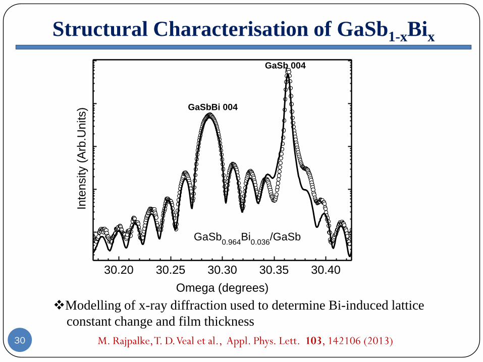
Structural Characterisation of GaSb1-xBix
28
Omega-2 theta scan of GaSb1-xBix on GaSb (001)
Lattice expansion upon Bi incorporation
S.K. Das, et.al. Infrared Physics & Technology 55
(2012) 156
Y.Song, et.al. J. Vac. Sci. Technol. B 30, 02B114 (2012)
x=0.05 x=0.036
Lattice
contraction
Lattice
expansion
M. Rajpalke, T. D. Veal et al.,
Appl. Phys. Lett. 103, 142106 (2013)
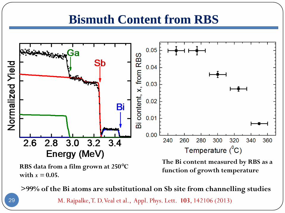
Bismuth Content from RBS
29
RBS data from a film grown at 250°C
with x = 0.05.
The Bi content measured by RBS as a
function of growth temperature
>99% of the Bi atoms are substitutional on Sb site from channelling studies
M. Rajpalke, T. D. Veal et al., Appl. Phys. Lett. 103, 142106 (2013)
30
Structural Characterisation of GaSb1-xBix
Modelling of x-ray diffraction used to determine Bi-induced lattice
constant change and film thickness
30.20 30.25 30.30 30.35 30.40
GaSbBi 004
Inte
nsity (
Arb
.Units)
Omega (degrees)
GaSb0.964
Bi0.036
/GaSb
GaSb 004
M. Rajpalke, T. D. Veal et al., Appl. Phys. Lett. 103, 142106 (2013)
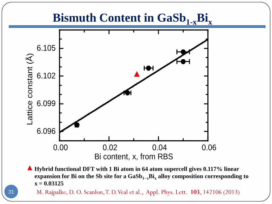
0.00 0.02 0.04 0.06
6.096
6.099
6.102
6.105
Lattic
e c
onsta
nt (Å
)
Bi content, x, from RBS
Bismuth Content in GaSb1-xBix
31
Hybrid functional DFT with 1 Bi atom in 64 atom supercell gives 0.117% linear
expansion for Bi on the Sb site for a GaSb1−xBix alloy composition corresponding to
x = 0.03125
M. Rajpalke, D. O. Scanlon, T. D. Veal et al., Appl. Phys. Lett. 103, 142106 (2013)

Kinetic Modelling of Bi Incorporation in GaSb1-xBix
32
The bismuth content, x, is given by Z. Pan.et.al, Appl. Phys. Lett. 77, 214 (2000)
C. E. C. Wood. et.al, J. Appl. Phys. 53, 4230 (1982)
M. J. Ashwin, T. D. Veal et.al, AIP Advances 1,
032159 (2011)
M. J. Ashwin,T. D. Veal et.al, J. Appl. Phys.113,
033502 (2013)
K is the rate constant for Bi incorporation, αJGa, where JGa is the incident Ga flux
α is a constant
NGa is the Ga atom density
JBi is the incident Bi flux
D is the bismuth desorption rate constant given by
Bi atoms
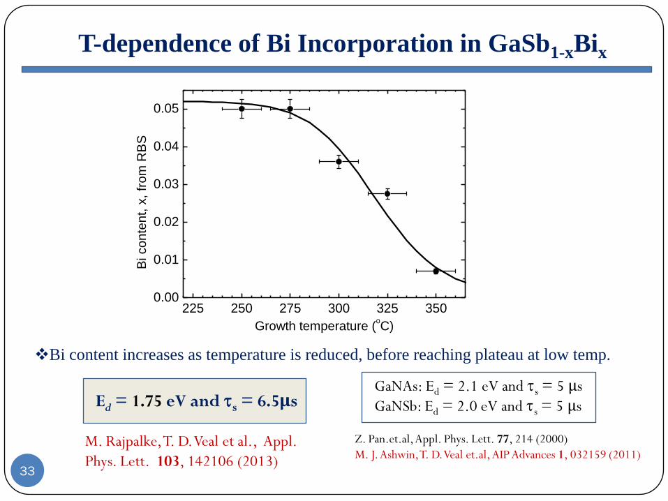
T-dependence of Bi Incorporation in GaSb1-xBix
Bi content increases as temperature is reduced, before reaching plateau at low temp.
Ed = 1.75 eV and s = 6.5μs
33
GaNAs: Ed = 2.1 eV and s = 5 μs
GaNSb: Ed = 2.0 eV and s = 5 μs
Z. Pan.et.al, Appl. Phys. Lett. 77, 214 (2000)
M. J. Ashwin, T. D. Veal et.al, AIP Advances 1, 032159 (2011)
225 250 275 300 325 3500.00
0.01
0.02
0.03
0.04
0.05
Bi co
nte
nt,
x,
fro
m R
BS
Growth temperature (oC)
M. Rajpalke, T. D. Veal et al., Appl.
Phys. Lett. 103, 142106 (2013)

34
Growth rate-dependence of Bi incorporation in GaSb1-xBix
M. Rajpalke, M. J. Ashwin, T. D. Veal et al., J. Appl. Phys. 116, 043511 (2014).
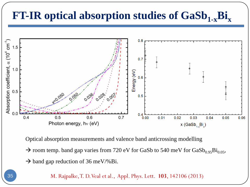
FT-IR optical absorption studies of GaSb1-xBix
35
Optical absorption measurements and valence band anticrossing modelling
room temp. band gap varies from 720 eV for GaSb to 540 meV for GaSb0.95Bi0.05,
band gap reduction of 36 meV/%Bi.
M. Rajpalke, T. D. Veal et al., Appl. Phys. Lett. 103, 142106 (2013)

Valence Band Anticrossing in GaSb1-xBix
36
Large band gap reduction with increasing Bi content
Not explained by the virtual crystal approximation
(VCA) alone
Need VCA lowering of CBM plus VBAC
M. Rajpalke, W. M. Linhart, T. D. Veal et al.,
Appl. Phys. Lett. 103, 142106 (2013)
T = 295 K
k.P method: K. Alberi et al.,
Phys. Rev. B 75, 045203 (2007)

37 K. Alberi et al., Phys. Rev. B 75, 045203 (2007)
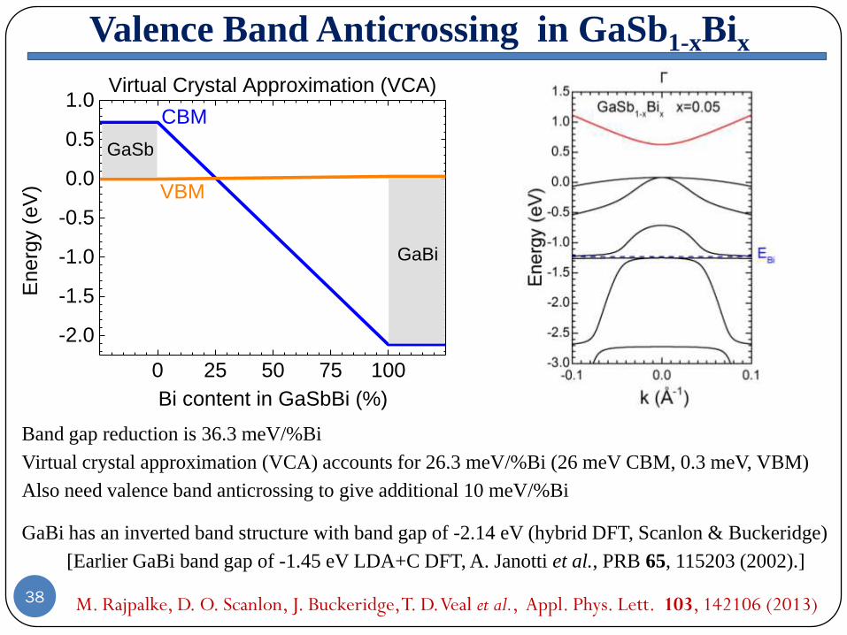
Valence Band Anticrossing in GaSb1-xBix
38
Band gap reduction is 36.3 meV/%Bi
Virtual crystal approximation (VCA) accounts for 26.3 meV/%Bi (26 meV CBM, 0.3 meV, VBM)
Also need valence band anticrossing to give additional 10 meV/%Bi
GaBi has an inverted band structure with band gap of -2.14 eV (hybrid DFT, Scanlon & Buckeridge)
[Earlier GaBi band gap of -1.45 eV LDA+C DFT, A. Janotti et al., PRB 65, 115203 (2002).]
M. Rajpalke, D. O. Scanlon, J. Buckeridge, T. D. Veal et al., Appl. Phys. Lett. 103, 142106 (2013)
0 25 50 75 100
-2.0
-1.5
-1.0
-0.5
0.0
0.5
1.0
GaBi
CBM
En
erg
y (
eV
)
Bi content in GaSbBi (%)
VBM
GaSb
Virtual Crystal Approximation (VCA)
39
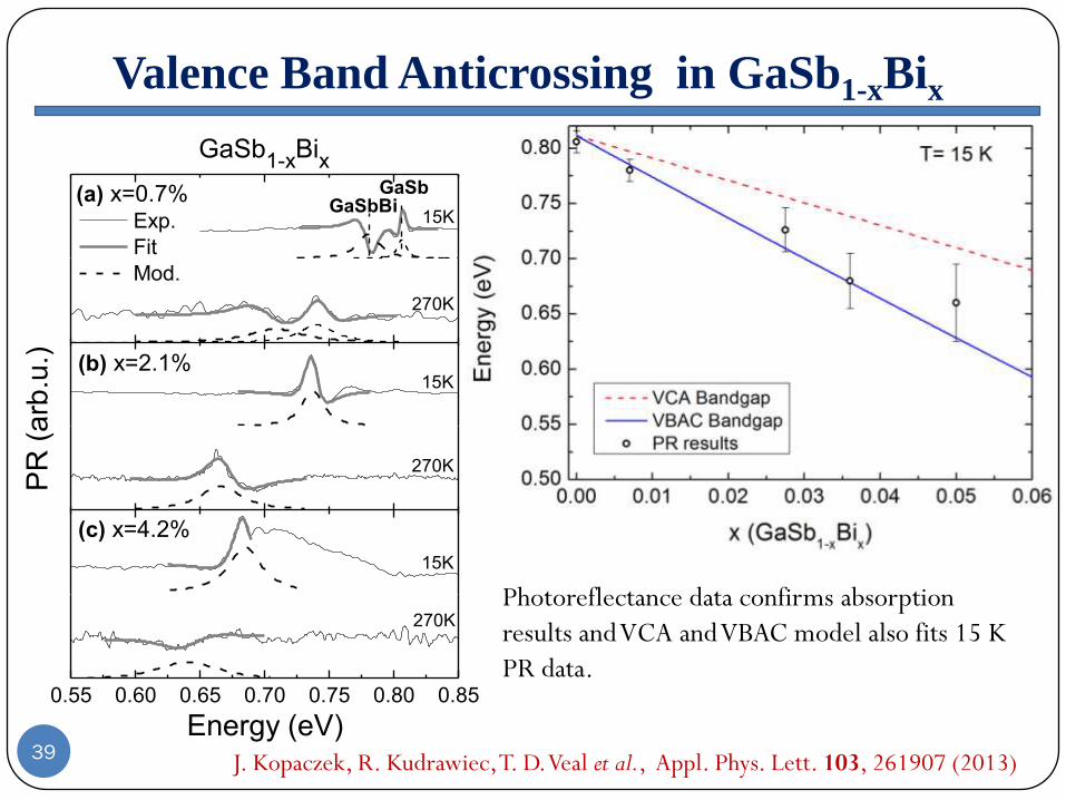
Valence Band Anticrossing in GaSb1-xBix
15K
Exp.
Fit
Mod.
270K
15K(b) x=2.1%
PR
(a
rb.u
.)
270K
15K
GaSbBi(a) x=0.7%
GaSb1-x
Bix
GaSb
0.55 0.60 0.65 0.70 0.75 0.80 0.85
270K
(c) x=4.2%
Energy (eV)
Photoreflectance data confirms absorption
results and VCA and VBAC model also fits 15 K
PR data.
J. Kopaczek, R. Kudrawiec, T. D. Veal et al., Appl. Phys. Lett. 103, 261907 (2013)

40
DFT density of states of GaSbBi with 10%
Bi compared with GaSb, illustrating role of
Bi 6s states in lowering CBM
M. Polak, T. D. Veal et al., J. Phys. D.: Appl. Phys. 47, 355107 (2014)
DFT calculation of GaSb1-xBix band gaps

41
T-dependence of GaSb1-xBix band gap from PR
0.60 0.65 0.70 0.75 0.80
x16x16x16
x16
x16
x8
50K
70K
90K
110K
130K
150K
170K190K
210K
230K
250K
270K
290K
30K
Energy (eV)
Ph
oto
refle
cta
nce
(a
rb.u
.) 15K
x=0.7%
x2
x4
x8
x16
0.60 0.65 0.70 0.75 0.80
GaSb1-x
Bix
50K
70K
90K
110K
130K
150K
170K
190K
210K
230K
250K
270K
290K
30K
Ph
oto
refle
cta
nce
(a
rb.u
.)
Energy (eV)
15K
x=2.1%
x2
x4
x5
x15
0.60 0.65 0.70 0.75 0.80
x6
x6
x2
x2
50K
70K
90K
110K
130K
150K
170K
190K
210K
230K
250K
270K
30K
Ph
oto
refle
cta
nce
(a
rb.u
.)
Energy (eV)
15K
x=4.2%
x2
x6
J. Kopaczek, R. Kudrawiec, T. D. Veal et al., Appl. Phys. Lett. 103, 261907 (2013)

42
T-dependence of GaSb1-xBix band gap from PR
0 50 100 150 200 250 3000.60
0.65
0.70
0.75
0.80
0.85 Exp. data
Varshni fit
B-E fit
En
erg
y(e
V)
Temperature (K)
x=0.7%
x=2.1%
x=4.2%
x=0%
GaSb1-x
Bix
0 50 100 150 200 250 300
10
15
20
25
30 x=0.7%
x=2.1%
x=4.2%
Fit by Eq.(5)
(
me
V)
Temperature (K)
GaSb1-x
Bix
• Band gap variation with temperature for GaSbBi is similar to that for GaSb
• Broadening of PR signal (intrinsic lifetime, alloy scattering) for GaSbBi is 5-10 times lower
than for InGaAsBi – due to lower size mismatch between Sb and Bi compared to As and Bi.
J. Kopaczek, R. Kudrawiec, T. D. Veal et al., Appl. Phys. Lett. 103, 261907 (2013)
43
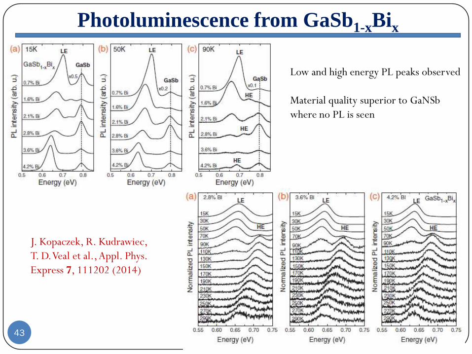
Photoluminescence from GaSb1-xBix
Low and high energy PL peaks observed
Material quality superior to GaNSb
where no PL is seen
J. Kopaczek, R. Kudrawiec,
T. D. Veal et al., Appl. Phys.
Express 7, 111202 (2014)
44
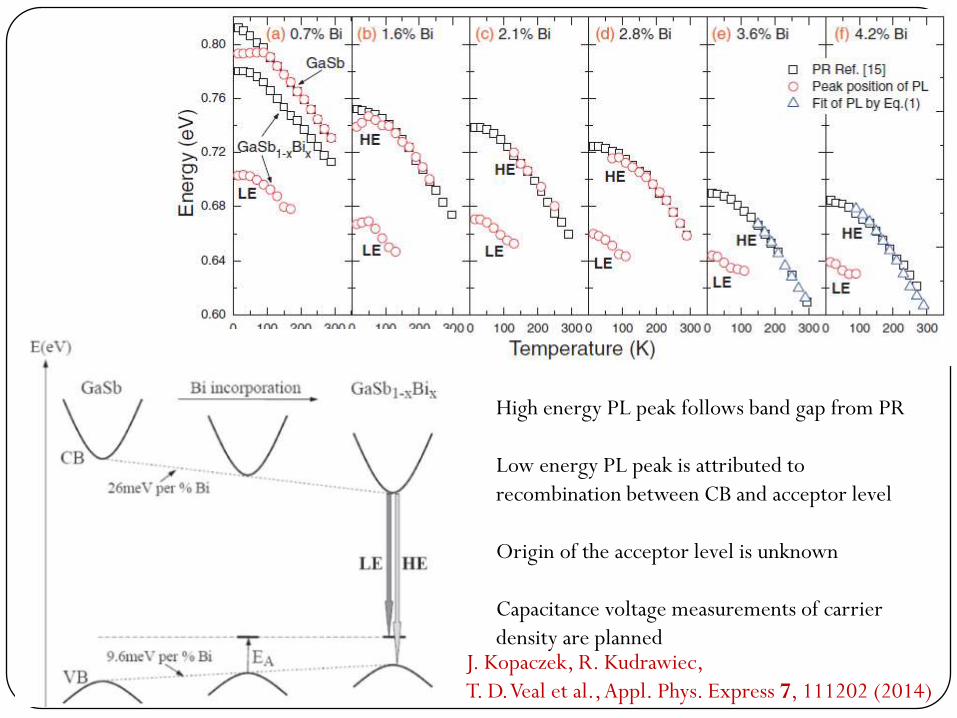
High energy PL peak follows band gap from PR
Low energy PL peak is attributed to
recombination between CB and acceptor level
Origin of the acceptor level is unknown
Capacitance voltage measurements of carrier
density are plannedJ. Kopaczek, R. Kudrawiec,
T. D. Veal et al., Appl. Phys. Express 7, 111202 (2014)

45
Band gap reductions per 0.01Å lattice constant change
GaBi
GaSb1-xBix
In one sense, GaSbBi is one of the
most extreme highly mismatched
alloys.
Band gap reductions for 0.01Å
change of lattice constant:
210 meV for GaSbBi
105 meV for GaNSb
157 meV for GaNAs
125 meV for GaAsBi
This is largely a consequence of the relatively close proximity of the GaSb and
zinc-blende GaBi lattice parameters.
M. Rajpalke, T. D. Veal et al., Appl. Phys. Lett. 103, 142106 (2013)
46
MBE growth of GaSbBi alloys up to 5% Bi incorporation
Lattice expansion observed, contrary to previous reports of MBE of GaSbBi
99% of the Bi atoms are substitutional from RBS
Reduction in band gap of 36meV/% Bi observed.
VCA and valence band anticrossing model fits absorption and PR data
Band gap change in GaSbBi is high per 0.01Å lattice constant change compared
with other highly mismatched alloys
GaSbBi alloys with band gaps in the range for domestic TPV (0.4 to 0.6 eV) have
been demonstrated.
Observation of photoluminescence suggests better quality than GaNSb. This is
expected due to better atomic size match between Sb and Bi than for Sb and N
Next steps: GaNSbBi alloys lattice matched to GaSb – only very small amounts of
N will be required, hopefully insufficient to turn the material to “cardboard”
Then doping and devices…
Conclusions:
47
Conclusions:
GaBi
GaSb1-xBix
0 25 50 75 100
-2.0
-1.5
-1.0
-0.5
0.0
0.5
1.0
GaBi
CBM
En
erg
y (
eV
)
Bi in GaSbBi (%)
VBM
GaSb
GaSbBi
GaNSb
Acknowledgments
48
RBS measurements at Lawrence Berkeley National Lab were supported the U.S. Department of Energy under Contract No. DE-AC02-05CH11231.
Calculations were funded by the EPSRC via the Centre for Innovation (EP/K000136/1 and EP/K000144/1) and the UK’s HPC Materials Chemistry Consortium (EP/F067496)
The work at Wroclaw is funded by the Polish National Science Centre (NCN grant no. 2012/07/E/ST3/01742)
Funding is acknowledged from University of Liverpool and the UK Engineering and Physical Sciences Research Council (Grant nos EP/G004447/2 and EP/H021388/1).
49
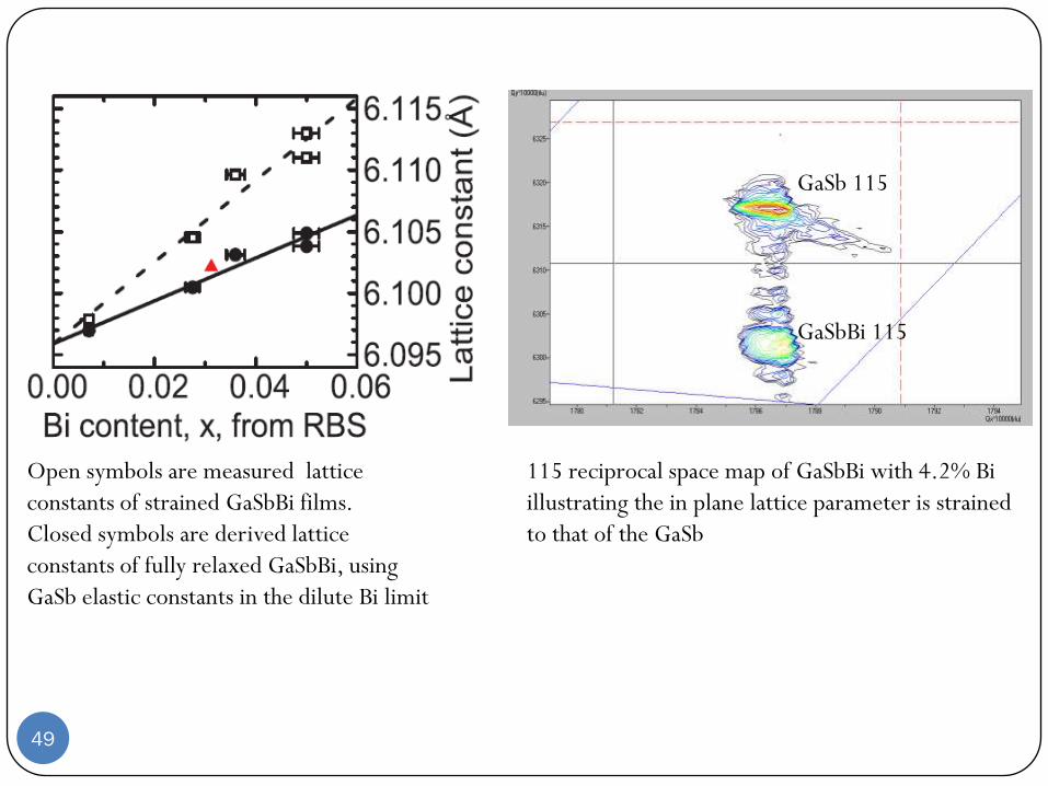
115 reciprocal space map of GaSbBi with 4.2% Bi
illustrating the in plane lattice parameter is strained
to that of the GaSb
GaSb 115
GaSbBi 115
Open symbols are measured lattice
constants of strained GaSbBi films.
Closed symbols are derived lattice
constants of fully relaxed GaSbBi, using
GaSb elastic constants in the dilute Bi limit
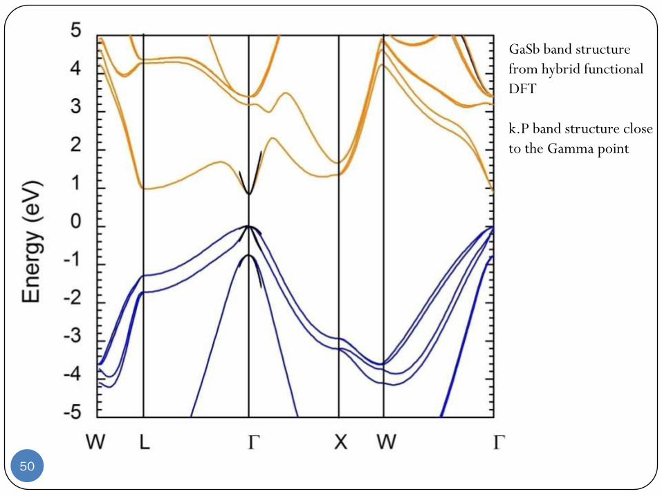
50
GaSb band structure
from hybrid functional
DFT
k.P band structure close
to the Gamma point