novel optimization tool for analog integrated circuits design
TRANSCRIPT
Czech Technical University in Prague
Faculty of Electrical Engineering
Doctoral Thesis
June 2013 Ing. Miloslav Kubař
Czech Technical University in Prague
Faculty of Electrical Engineering
Department of Microelectronics
Novel Optimization Tool
for Analog Integrated Circuits Design
Doctoral Thesis
Ing. Miloslav Kubař
Prague, June 2013
Ph.D. Programme: Electrical Engineering and Information technology
Branch of Study: Electronics
Supervisor: Ing. Jiří Jakovenko, Ph.D.

i
Acknowledgements
I am grateful to my supervisor Ing. Jiří Jarkovenko, Ph.D. for his patience and guidance
throughout my entire work. He has provided me with lot of valuable remarks, comment and
advices helping my thesis to be successful. He has led my work toward the goal and helped
me to overcome many difficulties. I also appreciate helpful advices and discussions of my
colleagues from the Department of Microelectronics.
I thank to my family for the valuable support, especially to my wife. She has encouraged
me greatly especially in the last years of my Ph.D. work.

ii
Table of Contents
Acknowledgements i
Content ii
Annotation iv
Anotace v
List of Used Abbreviations and Symbols vi
1 Introduction and Author’s Contributions 1
1.1 Background and Motivation 1
1.2 Organization of this Thesis 2
1.3 Objectives of the Work and the Scientific Contributions 3
1.4 State of the Art 6
1.5 Solution Methods of the Work 10
2 Optimization Algorithm 12
2.1 Evolutionary Algorithms 12
2.2 Differential Evolution 15
2.3 Differential Evolution Enhancements 19
3 Optimization Tool 22
3.1 User Interface 23
3.2 Optimization Tool Core 27
3.3 Simulator Interface 35
3.4 Optimization Watchdog 36
4 Design Examples 40
4.1 Two-Stage Miller OTA 45
4.2 Folded Cascode OTA 48
4.3 Voltage Regulator 51
4.4 New Design Example 54
4.5 Optimization Watchdog Verification 55
4.6 Comparison with Other Works 56

iii
5 Chip Design and Measurements 63
5.1 Chip Design 63
5.2 Measurement Board 68
5.3 Circuit Measurements 70
5.3.1 Two-Stage Miller OTA Measurements 71
5.3.2 Folded Cascode OTA Measurements 76
5.3.3 Voltage Regulator Measurements 81
6 General Conclusions 86
6.1 Discussion, Issues and Future Work 89
7 References 91
8 List of Publications 94
8.1 List of Works Related to the Doctoral Thesis 94
8.2 List of Works which are not Related to the Doctoral Thesis 94

iv
Annotation
The main goal of this Ph.D. thesis is to create an of the optimization tool (OT) for the
sizing of analog IC. The OT shall be usable in practise industry design work to save most of
the design time of basic generic circuits. Thus the proposed OT has a very short setup time, it
uses a robust optimization algorithm and produces accurate ready-to-use results.
Moreover I implemented two novel features to the OT. Optimization watchdog was
implemented to shorten optimization time, to improve convergence of the optimization and
thus to create better results. Also the novel feature called Advanced current mirror sizing
algorithm was developed and implemented. It serves for current mirror transistor sizing and
ensures a good transistor matching.
The OT is implemented in the GUI (Graphical User Interface) of the Cadence design
environment for the convenience of use. At the input, it is just needed to fill a form with the
specification for the desired circuit. The OT performs a full PVT (Process Voltage
Temperature) simulation automatically. Therefore the result of the optimization by the
designed OT is circuit that usually needs no additional schematic change and is ready for
layout.
The OT is implemented to the Cadence CIW (Command Interpreter Window) by the
Skill language. The core of the OT is created using Ocean scripting language. A robust
version of a differential evolution is used as the optimization method. An accurate simulation
based optimization approach was used for this tool.
Three types of analog circuits were optimized by the OT. The layout of these circuits
was designed, and the circuits were fabricated in the AMIS 0.35 μm technology by
Europractice. The verification of the OT was finalized by the chip measurements. Also the
complete design flow of the analog circuit from the circuit specification to the fabricated chip
measurements was finalized by the measurements.

v
Anotace
Hlavní cíl mé disertační práce je tvorba optimalizačního nástroje (ON) pro optimalizaci
analogových integrovaných obvodů. ON má být použitelný při praktickém firemním návrhu
obvodů, aby ušetřil většinu času potřebného při návrhu libovolných základních obvodů. Proto
navržený ON potřebuje velmi krátký čas pro svoje nastavení, užívá robustní optimalizační
algoritmus a vytváří přesné obvody.
Navíc jsem do ON přidal dvě zcela nové funkce – optimalizační hlídač – pro zkrácení
doby optimalizace a zlepšení konvergence optimalizace, tudíž pro možnost tvořit lepší
obvody. Dále jsem implementoval novou funkci pro návrh proudových zrcadel. Tato funkce
umožňuje návrh proudových zrcadel s malým proudovým rozptylem.
Kvůli snadnému používaní je ON integrován do grafického uživatelské rozhraní
návrhového prostředí Cadence. Stačí pouze vyplnit formulář se specifikací obvodu a počkat
na výsledky. ON simuluje obvod ve všech rozích (technologických, napájecích a teplotních),
takže výstupem optimalizace je obvod, který obvykle nepotřebuje žádnou změnu a je
připravený k layoutu.
ON je integrováno do návrhového prostředí Cadence pomocí jazyka Skill. Jádro ON je
vytvořeno pomocí skriptovacího jazyka Ocean. Robustní verze diferenční evoluce je použita
jako optimalizační metoda. Optimalizace je založena na obvodových simulacích, což vede
k přesným výsledkům.
Pomocí ON byly optimalizovány tři typy analogových obvodů, byl vytvořen jejich
layout a dále čip byl vyrobený v AMIS 0,35 μm technologii ve firmě Europractice. Měřením
těchto čipů byla ověřena funkce ON a také uzavřen proces návrhu od specifikace až po měření
vyrobeného čipu.

vi
List of Used Abbreviations and Symbols
List of Abbreviations
AC Alternating Current
CAP Capacitor
CIW Command Interpreter Window
CMOS Complementary Metal-Oxide-Semiconductor
CPU Central Processing Unit
DC Direct Current
EA Evolutionary Algorithm
GUI Graphical User Interface
IC Integrated Circuit
LVT Low Voltage Transistor
MPW Multi Purpose Wafer
NMOS N channel Metal-Oxide-Semiconductor transistor
OT Optimization Tool
OTA Operational Transconductance Amplifier
PMOS P channel Metal-Oxide-Semiconductor transistor
PVT Process Voltage Temperature
RAM Random Access Memory
RES Resistor
List of Symbols
A0 gain
BW Bandwidth
CMRR Common Mode Rejection Ratio
CR Crossover Ratio (probability)
DTMP Temperature Drift
F Fitness Function
GBW Gain Bandwidth
IB Bias Current

vii
IDD Current consumption
IL Load Current
L Length
n Population size
PM Phase Margin
PSRR Power Supply Rejection Ratio
REGLD Load Regulation
REGLN Line Regulation
SF Scaling Factor
SR Slew Rate
Temp Temperature
VDD Positive voltage supply
VGS Gate-Source Voltage
VIN Input Voltage
VREF Reference Voltage
VSS Negative voltage supply
VTH Threshold Voltage
W Width
WDC Watchdog - Count
WDD Watchdog - Difference
WDP Watchdog - Populations
(further abbreviations and symbols are explained in the text)

1
1 Introduction and Author’s Contributions
1.1 Background and Motivation
ICs are used in every industry field at present. Demands on their performance are
increasing rapidly. Therefore their complexity and the number of devices in one IC is growing
quickly.
Since the digital part of a chip usually covers 90 % of the chip area, the development of
IC technology focuses mainly to improve digital circuits. The switching time, the complexity
and the power consumption are the main criteria that push the IC technology towards shorter
L of the transistors. Thus the chip area is reduced, the operating frequency is increased and
the supply voltage is lowered decreasing power consumption.
The software to automate design of the chip digital part is available and frequently used
for many decades. Digital synthesizers from hardware description language (HDL) and tools
for place and route of the synthesized net-list into the final optimized layout are used in
everyday industry work, saving a lot of the digital circuit design time.
Analog part of the IC covers just about 10 % of the chip area. But, the design and
validation of this part takes about 90% of the time needed to design the whole circuit. This
portion increases because of the trends in IC technology development. The requirements of a
lower supply voltage and shorter transistor L make the analog design more complicated and
challenging.
The aforementioned reasons lead to the growing needs for robust tools that would
automate certain parts of the analog design flow. An automated design of the analog circuits
can save an enormous part of the design time and expenses needed to design the chip. At
present, much effort is being spent to develop an analog synthesis tool or OT that would
shorten the design time of the analog circuits. Many scientists and research institutions all
around the world have been trying to develop and improve such a tool [1][2][3][4][5].
It is not usual that the design teams use tools for automated design for the analog part of
the IC. The development of OT is not in such a stage yet to be able to use it in industry design
fully. While commercial optimization tool [6] exists, it is used only as a support tool, for
example to fine tune a certain parameter of an already designed circuit. This tool is not used
to create final schematics of an analog circuit from scratch.
2
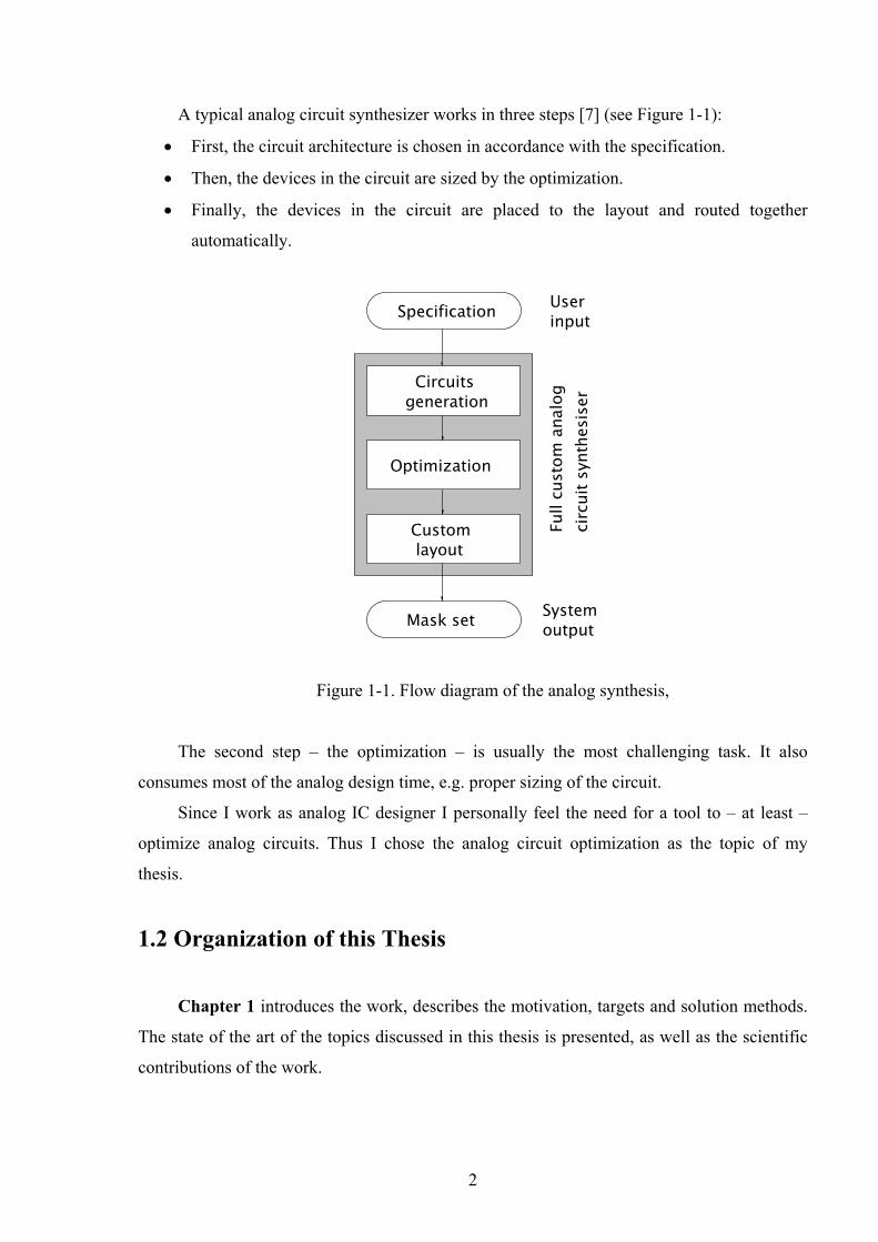
A typical analog circuit synthesizer works in three steps [7] (see Figure 1-1):
• First, the circuit architecture is chosen in accordance with the specification.
• Then, the devices in the circuit are sized by the optimization.
• Finally, the devices in the circuit are placed to the layout and routed together
automatically.
Mask set
Specification Userinput
Systemoutput
Full
cust
om a
nalo
gci
rcui
t syn
thes
iser
Circuitsgeneration
Custom layout
Optimization
Figure 1-1. Flow diagram of the analog synthesis,
The second step – the optimization – is usually the most challenging task. It also
consumes most of the analog design time, e.g. proper sizing of the circuit.
Since I work as analog IC designer I personally feel the need for a tool to – at least –
optimize analog circuits. Thus I chose the analog circuit optimization as the topic of my
thesis.
1.2 Organization of this Thesis
Chapter 1 introduces the work, describes the motivation, targets and solution methods.
The state of the art of the topics discussed in this thesis is presented, as well as the scientific
contributions of the work.
3
Chapter 2 “Optimization Algorithm” contains details of the optimization algorithms.
Mainly, evolutionary algorithms are listed as they were found to be suited best for the analog
circuit sizing task. Moreover, differential evolution – the optimization algorithm chosen for in
this work – is described in more detail, together with the recent improvements of this method.
Reasons of this choice are given.
Chapter 3 “Optimization Tool” describes the OT created for the analog circuit sizing.
Details about the OT algorithm are given together with those about the user interface that was
created to facilitate the usage of the OT. A detailed description of the OT core script, the
interface between the OT and the Spectre circuit simulator used to extract the values of the
circuit parameters and novel Optimization watchdog feature are listed further. The procedure
to change the fabrication technology is described.
Chapter 4 “Design Examples” presents the details about the design examples
implemented to the developed OT. Optimizations of those examples are presented.
Verification of the novel optimization watchdog feature verification is described. Procedure to
implement an arbitrary analog circuit design examples is discussed as well as design in
different technology. Finally, comparison with other optimization procedures presented
recently is given. The novel current mirror sizing feature is described.
Chapter 5 “Chip Design and Measurements” describes measurements of the chip
containing optimized circuits. Chip design and layout are presented. Measurements board
description and all circuit measurements are given. The measurements are discussed together
with comparison simulations.
Chapter 6 gives general conclusions of my work, scientific contribution of my thesis,
discussion of concerned issues and future research plans.
1.3 Objectives of the Work and the Scientific Contributions
This work is mainly focused on the optimization of analog circuits. During the
completion of my thesis I decided to change its original title (defined at the beginning of my
research) from Design and optimization of the linear low-power regulators for integrated
circuits to the current one, which captures the scope of the work more appropriately. I
extended the scope of my work by additional research areas. So, a new title Novel
optimization tool for analog integrated circuits design has been chosen. My research was not
focused strictly on voltage regulators optimization. Rather, an automated design of several

4
types of analog circuits was included in this thesis. Moreover, I worked on the creation of a
novel OT for everyday industry design work. This OT was presented at the Workshop on
Symbolic and Numerical Methods, Modeling and Applications to Circuit Design (SM2ACD)
in Tunisia [8]. The tool shall be able to generate sized circuit schematic ready for the
application, reducing the design time significantly. The optimization of a voltage regulator –
the original scope of my work – was also performed using the newly developed design tool.
The main goal of this work was to create an OT that shall be able to size the devices of
various analog circuits in accordance with their circuit specification. The resulting OT was
tested successfully on the optimization of two OTA architectures and one voltage regulator
architecture. The presented tool is universal and can be used to optimize circuits of any type
and architecture.
The OT was enhanced by two novel features that were developed in this thesis. The
Optimization watchdog reduces the optimization time of the design task and makes it possible
to converge to better results. The Advanced current mirror sizing algorithm generates current
mirrors with good matching and thus with a higher accuracy. These novel features were
presented in the Radioengineering journal [9].
The tool was verified by measurements of the chip containing optimized circuits to
cover the complete analog circuit design flow from the circuit specification to the fabricated
chip measurement.
The novel OT shall be usable in the industry design work, satisfying the following
requirements:
• Very short setup time of the OT. This is the time needed to setup the tool according to
the specific design task before the automated optimization is started. If the setup time
was long (several hours or even days) the development of the circuit using standard
design ways would be equivalent to the automated one or even shorter.
• Accurate ready-to-use results produced by the novel OT. The optimization of the
circuit must take into account PVT corners because the PVT analysis is able to find
the worst case of each specified circuit parameter. Moreover, the simulations of the
optimized circuit must be done by using realistic models of the devices used in IC
technology (transistors, resistors, capacitors etc.). This makes the results of the
automated design more reliable.
• Robustness of the tool. The OT must be able to converge to the solution for a generic
circuit, specification and initial conditions (not only for limited range of circuits). An

5
application of a robust optimization algorithm is also needed to ensure the
convergence to the global extreme and not stuck during the optimization course.
The tasks solved in the thesis are listed below:
• Creation of the OT for analog circuit optimization.
o Design of the OT core – implementation of the chosen optimization algorithm.
o Design of a OT user interface to reduce the OT setup time.
o Implementation of the PVT analysis to make possible a robust circuit design in
a reasonable time.
• Design and implementation of an Optimization watchdog feature.
o Feature design and implementation to the optimization algorithm.
o Verification of its benefits on design examples optimization.
• Novel algorithm of the current mirror design.
o Simulation of mirror transistors for different currents.
o Creation of the algorithm for automated transistor sizing.
o Implementation of the novel algorithm to the OT.
• Optimization of several analog circuits using the OT to verify its function.
o Design of the test-benches needed to extract circuit parameters.
o Using the OT to optimize the circuits.
• Creation of a chip - containing the optimized circuits - to verify the complete design
flow from the specification to the measurement of the chip.
o Chip design.
o Chip layout.
o Fabricated chip measurements.
Scientific contributions of this work are:
• The Optimization watchdog feature reduces the design space during the course of
optimization, improving both convergence and the quality of the results.
• The first OT ever that is able to optimize an analog circuit by means of a full PVT
simulation using real technology models.
• OT with very short setup time.
o No need to create circuit schematic, test-benches and define extraction of the
circuit parameters.

6
o OT implemented to the widely used design environment.
• Possible optimization of a generic circuit.
• Optimization independent of the design technology.
• Novel algorithm for the design of accurate current mirrors.
• Verification of the OT by the measurement of the chip containing circuits optimized
by the created OT.
1.4 State of the Art
The topic of the analog circuit synthesizer is quite old [7] and has generally been
considered a difficult problem [2]. No powerful, reliable and versatile tool for automated
analog circuit design has been created yet. No optimization tool is widely used in industry
analog circuit design.
The approaches to automate the analog design that have been published so far for typical
analog ICs are [10][11]:
• Knowledge based [2]. They are first to appear. They are defined by including a
complete design plan describing how the circuit components must be sized to solve
the design problem. But, there is no guarantee of finding the optimum solution. The
main idea of this approach is to encapsulate the designer’s knowledge to build a pre-
design plan. The plan contains design equations and a design strategy that produces
the component sizes in order to meet the performance requirements. The drawback of
these approaches is the large amount of work needed to define a new design plan. It is
necessary to reformulate the entire design plan when expanding the system to new
technologies. Another disadvantage is the time consuming encoding of the design
knowledge for a given set of specifications.
The three following approaches to design automation are optimization based. They use
an optimization engine instead of a design plan to perform the design task. The optimization
process is an iterative procedure where the design variables are updated in each iteration until
an equilibrium point is reached. The optimization algorithm searches through the design space
for values of each circuit component. The performance evaluation tool verifies if the
performance constraints are met.

7
• Equation based approaches [3][12][13] use analytic design equations to evaluate the
circuit performance. These equations can be derived manually or automatically by
symbolic analysis tools. Then, the problem can be formulated as an optimization
problem and usually solved using a numerical algorithm. The main drawback is that
analytical models have to be used to derive the design equations for each new
topology. Another drawback is that, despite recent advances in symbolic circuit
analysis, not all design characteristics can be easily captured by analytical equations.
The approximations introduced in the analytical equations yield a low accuracy design
especially in complex circuit designs.
• Simulation based approaches [14][15][16][17] use simulations to evaluate the circuit
performance. The optimal values of circuit parameters are extracted from the
simulation results. This is pointed out as a very flexible solution when compared with
other methodologies (equation-based, knowledge-based) because it can be
accommodated to any type of circuit topology and yields a superior accuracy
(depending on the device models). The same circuit can be optimized several times for
different specifications as long as the fitness function is adapted. Therefore virtually
all types of circuits can be optimized with a short setup time with this approach. The
drawback of these methods is that it is computationally very expensive to evaluate the
performance of the optimized circuit by electrical simulations.
• Learning strategy based [18][19]. The behavior of the circuit to be optimized is
modeled by a learning mechanism based on the distribution of variations. It allows a
quick evaluation of the performance for a specific set of design parameters, which is
clearly more time efficient. A set of training samples must be evaluated at the
beginning of the optimization with a high-accuracy evaluation engine like the circuit
simulator, which increases the setup time. The amount of training data will influence
the accuracy of the performance predictions made by the learning machine. Like in the
equation-based methods, there will always be a trade-off between accuracy and
efficiency.
The equation based methods are not accurate enough to design analog ready-to-use
circuits automatically. The learning based strategies can produce powerful circuits but their
setup time can be longer than a design without any OT because of the creation of training
samples. The simulation based tools produce the most accurate circuits and the setup time is

8
the shortest. Therefore the simulation based approach was chosen despite the fact that the
computation time is the longest in this approach [11].
Many studies about the automated analog circuit design published recently are quite
sophisticated and present powerful analog circuit synthesis ideas and improvements. On the
other hand, these approaches or the principles they present are not really usable in industry
OT since they do no meet the requirements mentioned in Chapter 1.3.
The optimization methods [3][14][20][21] use equation based optimization method that
produces not very accurate results generally. The reason is that the equation based
optimization uses just a simplified description of the circuits by the equations and usually uses
simplified transistor models.
Labrar et al. [22] use an equation based rough pre-optimization, which can be also
difficult for more complex circuits that are not easy to describe by equations. This work uses
it to describe the well know two-stage Miller OTA.
The optimization method used by Pereira-Arroyo et al. [12] generates only a map of
results and the user needs to choose the solution manually. This can take a long time in case
of complicated designs.
The automation algorithm presented by Jafari et al. [1] uses a simulation based method
only in the initialization phase, and this may lead to inaccurate results.
Somani et al. [2] use a knowledge based initial setup in their method, resulting in a long
setup time.
The method presented by Bo et al. [4] is not very robust since it would take a long time
to find the value of the penalty coefficient, which is used in their tool. The search for
coefficients can cause a long setup time as well.
The tool presented by Barros et al. [18] is not very useful since a long setup time is
required with their learning strategy. The accuracy of the tool is questionable as well because
it depends on the number of training samples strongly.
OT presented by Mishra et al. [19] uses a knowledge based learning mechanism. It can
be inaccurate, cause wrong decisions and it can be also problematic for more complex
circuits.
The algorithm presented by Fakhfakh et al. [5] just replaces all of the design variables
by a single variable (substitution), making it impossible to use the most accurate simulation
based optimization approach.
The optimization approach presented by Thakker et al. [15] would not produce a very
robust design because of performing PVT (Process Voltage Temperature) corner simulations

9
after the optimization to save the computation time. Moreover, Doménech-Asensi et al. [23]
presented a tool that does not perform a PVT analysis at all.
A quite powerful commercial tool [6] is used widely to automate the design work partly.
It is very difficult to design circuits purely automatically. It needs a long setup time to create
the test-benches needed for the optimization. It also requires manual definition of the design
task that can take longer time than optimization using the proposed tool. The created design
examples are also technology dependent. Moreover, the optimization method is not under
control. Note that this is the opposite in the proposed optimization method using the novel
optimization watchdog feature.
The state of the art of the analog circuit design automation is described in [10][11] well.
Moreover, the open research points in this field are discussed in [10]. The main open points of
the automated analog circuit sizing to be solved in the future are:
• Definition of design variables bounds (design space limitations) to ensure the
feasibility of the optimal solution. The limits must be set to also ensure a good
matching of the devices and a reasonable circuit area. A wide design space enables the
OT to find a better circuit, but the convergence is very slow, thus the time required to
find a powerful circuit can be very long.
• The tuning of the multi-objective evolutionary algorithms to deal with different types
of ICs and IC technologies (mainly for nanometer technologies). The performance of
the analog IC does not scale with the scaling of W/L dimensions of the transistors and
can introduce a significant complexity because of the high parameter dimensionality.
• Sets of feasible solutions can be found by analog circuit sizing. To find the optimal
solution among the feasible ones is quite problematic.
I have proposed a novel feature to deal with the first open point described above – to
reduce the design space of the optimization task (to reduce the intervals of width and length of
the transistors in the design) by means of a novel optimization watchdog feature. This
reduction leads to a faster convergence of the optimization and thus to the reduction of the
computation time. It also helps the optimization algorithm to find a better circuit if the design
space is limited to an area that does not include the optimal circuit.
I have implemented another novel feature, to size the current mirror transistors to be
more accurate than the approaches used in [16][17][24][25][26]. It is based on transistor
sizing dependent of the current flowing through the transistor. The transistor sizes are based
on interpolation or extrapolation using a look-up table with simulated transistor sizes.

10
1.5 Solution Methods of the Work
Since a lot of companies all around the world use Cadence design environment, the OT
user interface developed in this work is implemented in the main Cadence CIW. This kind of
implementation has been used to ensure easy usage of the OT and to minimize the setup time.
A new “Optimize” toolbar has been introduced by a script written in the Skill language [27],
exploiting the modular characteristic of the Cadence design environment, which written in
Skill and can extended using this language. A modification can be inserted conveniently as a
module/script in text format, which is loaded by Cadence at start-up.
The new toolbar contains a sub-menu for each circuit type that can be optimized by the
proposed OT. The specification of the circuit is filled in a simple form that appears after
choosing the type of circuit to be optimized. This form can be filled very quickly, ensuring a
very short setup time of the new OT. The OT core is executed after the form has been filled.
The OT core is written as an Ocean [27] script. This language is made by Cadence thus
cooperate with Cadence and Skill scripts well. The main reasons to implement the OT core in
the Ocean scripting language are:
• An Ocean script can be launched from the Cadence CIW by a Skill script.
• The mathematical function of the optimization algorithm can be programmed in an
Ocean script.
• Pre-created net-lists of the circuits to be optimized can be loaded by the Ocean script.
• Ocean can run Spectre simulation to perform circuit analysis.
• Spectre simulation results can be post-processed by Ocean to extract the circuit
parameters.
• The corners of simulations can be controlled by the script to perform PVT simulations.
• The parameters (design variables) of the circuit that is being optimized can be loaded
from a parameter file for the Spectre simulator.
Text output files are created by the script. These files contain details of the optimization
process. Thus the optimization progress is track-able, enabling to assess the circuit,
specification and bounds of the design variables.
The OT core uses net-list of the test-benches of the optimized circuits, enabling the
execution of circuit simulations to extract parameters of the circuit, which is optimized. These

11
test-benches and their net-lists are pre-created for the OT in the Cadence design environment
for each circuit, which can be optimized by the proposed OT.
The Optimization watchdog is simple but effective algorithm, which requires for its
function only several variables and several arithmetic operations to be defined. It has been
implemented to the OT core by the Ocean language.
The current mirror design algorithm is based on several simulation of transistor. The
results of these simulations are implemented to the OT by the definition of several variables.
The arithmetic operations needed by the algorithm (interpolations and extrapolations of the
simulated values) are implemented using the Ocean language.
The circuits optimized by OT are designed in the AMIS 0.35 μm CMOS technology and
are optimized by PVT simulations. The technology can be changed – see Chapter 3.3 for more
details.
The circuit optimizations are tested. The layout of the chip containing the optimized
circuits is created in the Cadence Virtuoso tool and the gds data are sent to Europractice to be
manufactured. Finally, the parameters of the optimized circuits are measured to verify the OT
and to complete the design flow from the circuit specification to the fabricated chip
measurements.

12
2 Optimization Algorithm
Recently requests to optimize various engineering tasks appeared. Examples of these
tasks can be fuel consumption of jet engines or wall thickness of pressure tanks. Electrical
tasks as analog IC designs can be found as well [28].
Solving of these electrical examples is transferred to pure mathematical problems.
Optimization tasks are usually defined by properly defined cost (fitness) function. Solving of
these problems is done by finding minimum (maximum) of the cost function. Analytical
solution of these tasks is sometimes possible but usually complicated and lengthy. Therefore
optimization algorithms are used to find extremes of the cost function.
Suitable optimization method is required to make a robust OT for analog IC design. I
needed an algorithm that is able to optimize analog circuits (multi-objective optimization task
using real numbers). Moreover robust method is needed to be able to optimize a generic
circuit and converge to the global extreme.
Typical optimization methods (like gradient based algorithms) that are frequently used
in OT have several drawbacks. They can be easily trapped in local minimum, need good
initial conditions, can not optimize more complex circuits, can not optimize circuits using
realistic models of its devices, can not optimize multi-criterion tasks etc.
Evolutionary algorithms (subgroup of the so called heuristic algorithms) proved to
overcome those difficulties and be good candidates for analog circuit sizing tasks [29][30].
They are designed to converge to the global extreme because of their stochastic behavior [13].
These techniques are also well suited for multi-criterion optimization [14] which is the case of
analog circuit optimization.
2.1 Evolutionary Algorithms
The members of one generation fight among each other in nature to survive and to
reproduce themselves. The result of the fight is based on the strength of the individual and its
adaptation to the environment. The structure of the population evolves. This evolution is
based on Darwin’s law of the natural choice. The individual that survives has the biggest
strength and fitness.
Evolution algorithms use models of the evolution processes that can be found in the
nature. They use it to find the solution of the complex and hard tasks. They work with

13
populations of individuals (circuits in our case). Evolution of these individuals is simulated.
Each individual represents vector of design variables (for example widths and lengths of the
transistors in the designed circuit). A rating (fitness) of each individual is then computed
using fitness function. This rating represents the deviation of the individual parameters from
the specified parameters. This rating also determines the progress of the search through the
design space [28][29]. Evolutionary algorithms use mechanisms inspired by biological
evolution [30][31]:
• Reproduction – new offspring individual is produced from its parents.
• Mutation – the offspring is altered (usually randomly) from its parents due to an error
in the genetic information (due to an external force).
• Recombination – altered genetic information of the offspring is generated as the
combination of the genetic information of the (two or more) parents.
• Selection - the offspring with more fitness is selected to the next population.
Similar evolutionary techniques differ in the implementation details and the nature of
the particular applied problem [31]:
• Genetic algorithm - one seeks the solution of a problem in the form of strings of
numbers (usually binary, although the best representations are usually those that
reflect something about the problem being solved). It is done by applying operators
such as recombination and mutation (sometimes one of them, sometimes both). This
type of EA is often used in optimization problems.
• Genetic programming - here the solutions are in the form of computer programs and
their fitness is determined by their ability to solve a computational problem.
• Evolutionary programming - similar to genetic programming. But the structure of the
program is fixed and its numerical parameters are allowed to evolve.
• Gene expression programming (GEP) - like genetic programming GEP also evolves
computer programs but it explores a different (genotype-phenotype) system. Computer
programs of different sizes are encoded in linear chromosomes of fixed length in this
system.
• Evolution strategy - works with vectors of real numbers as representations of
solutions. It uses self-adaptive mutation rates typically.

14
• Differential evolution - based on vector differences. It is therefore primarily suited for
numerical optimization problems. I chose it for my OT. See Chapter 2.2 for reasons
for that choice and more details about the differential evolution.
• Neuro-evolution - similar to genetic programming. The genomes (the information that
characterizes a specific individual completely) represent artificial neural networks by
describing structure and connection weights. The genome encoding can be direct or
indirect.
• Learning classifier system (LCS) - an adaptive system that learns to perform the best
action given by its input. An LCS is "adaptive" in the sense that its ability to choose
the best action improves with experience. This experience is usually gained by testing
of some number of test individuals.
All these evolution algorithms have several common features:
• They work with complete group of possible solutions more likely than with one single
solution.
• First population is generated randomly (in the design space).
• They improve the solution step by step by trying of new candidate solutions. These
possible solutions are generated as a combination of the previous solutions.
• Combinations of the possible solutions are followed by random changes and
elimination of the inadequate possible solutions.
• Population of specific number of individuals is repeatedly recreated and modified to
find as good solution as possible.
• Algorithm usually ends by finding the optimum solution or after predefined number of
population generations.
Combinations of the evolutionary algorithms and gradient-type methods were found to
be more efficient than evolutionary algorithm only. Combined method of differential
evolution and Gauss-Newton algorithm was presented in [32]. Combined method of specific
genetic algorithm and Lavenberg-Marquardt method was published in [33]. Both algorithms
combine advantages of genetic algorithm to be able to converge to the global optimum and
fast convergence speed of the gradient-type methods. Nevertheless I can not use similar
algorithms. The reason is that derivations requested by the gradient-type algorithm can not be
computed in simulation based OT.

15
2.2 Differential Evolution
Differential evolution optimization algorithm was developed by Storn and Price [34]. It
belongs to the group of evolutionary algorithms that works with functions of several real
variables. They presented this algorithm in 1996 and in the same year differential evolution
was outstanding at the First International Contest on Evolutionary Computation held in
Nagoya. Differential evolution turned out to be the best evolution type of algorithm for
solving the real-valued test function [29][28][35][36]. Differential evolution was found to be a
very good choice for analog circuit sizing [13] [35][37] in terms of:
• Optimization stability of non-convex, multi-modal and non-linear functions.
• Rapid convergence speed.
• Solving multi-variable real-valued functions.
• Operations of the differential evolution are simple and easy to program.
• Simple and efficient algorithm.
Differential evolution uses three main parameters during its optimization process
[35][38]:
• n - population size.
• SF - scale factor.
• CR - crossover probability.
The basic version of the differential evolution optimization algorithm is explained
below. Simple example using single-stage OTA (Figure 2-1) zero-frequency gain
optimization is used for this explanation.
The gain (fitness of the circuit in this case) is optimized in this example by three design
variables:
• ibias - bias current.
• wdif - width of the transistors in the differential pair.
• wmir - width of the transistors in the active load.

16
vdd
vss
inninp
out
ibias
wdifwdif
wmir wmir
Figure 2-1. Single-stage OTA.
The optimization process is composed from 4 steps [35][39] and is shown on Figure 2-2
for better understanding:
• Initialization - first step of the optimization is to randomly generate - but in specific
range (design space) – first population. The population has 6 individuals in this
example (n = 6). The design variables (ibias, wdif and wmir) of each individual
(circuit) are randomly chosen in the ranges defined by the bounds of each design
variables. Those ranges/bounds define the design space of the optimized circuit. Then
the fitness (gain of the optimized circuit in this example) of each individual in the
population is computed (for example by the circuit simulation). More circuit
parameters are optimized usually together. Then the fitness function is necessary for
the circuit fitness determination (see Chapter 2.3 for the fitness function used in my
OT).
• Mutation – is done for each (target) individual in the population. Three random (and
different from each other and different from the target individual) individuals are
chosen from the current population. The second, third and fifth individuals are chosen
for the first one in this example. Each design variable of the third individual are
subtracted from the variables of the second individual and the result is multiplied by
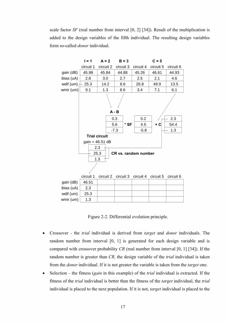
17
scale factor SF (real number from interval [0, 2] [34]). Result of the multiplication is
added to the design variables of the fifth individual. The resulting design variables
form so-called donor individual.
gain (dB)ibias (uA)wdif (um)wmir (um)
circuit 1 circuit 2 circuit 3 circuit 4 circuit 5 circuit 6I = 1 A = 2 B = 3 C = 5
A - B
* SF + C
Trial circuit
gain (dB)ibias (uA)wdif (um)wmir (um)
circuit 1 circuit 2 circuit 3 circuit 4 circuit 5 circuit 6
CR vs. random number
gain = 46.51 dB
45.98 45.84 44.88 45.26 46.61 44.932.8 3.0 2.7 2.5 2.1 4.625.3 14.2 8.6 26.8 49.9 13.59.1 1.3 8.6 3.4 7.1 6.1
0.3 0.2 2.35.6 4.5 54.4-7.3 -5.8 1.3
25.32.3
1.3
46.512.325.31.3
Figure 2-2. Differential evolution principle.
• Crossover - the trial individual is derived from target and donor individuals. The
random number from interval [0, 1] is generated for each design variable and is
compared with crossover probability CR (real number from interval [0, 1] [34]). If the
random number is greater than CR, the design variable of the trial individual is taken
from the donor individual. If it is not greater the variable is taken from the target one.
• Selection – the fitness (gain in this example) of the trial individual is extracted. If the
fitness of the trial individual is better than the fitness of the target individual, the trial
individual is placed to the next population. If it is not, target individual is placed to the

18
next population. This procedure is done for each individual in the population resulting
in new population.
Last three steps are repeated over and over to create new populations until the fitness
(gain in this example) of some individual meets the specified objective (in this example until
the gain is higher or equal to the specified value defined by user of the OT). The flow diagram
of the differential evolution algorithm is shown on Figure 2-3.
First population generation
First populationfitness extraction
Mutationoperation
Crossoveroperation
Selectionoperation
No Yes
End
Begin
Satisfy endcondition ?
No
Output results
Satisfy endcondition ?
Yes
Figure 2-3. Differential evolution flow diagram.
There is a danger of the dead lock in the OTs based on differential evolution. It can
happen when the specification is set too demanding. Then the optimization algorithm is
creating new populations over and over, it never gets to the solution thus never ends. It is
usually solved by setting of the maximum number of the population to be created.
19
2.3 Differential Evolution Enhancements
The basic version of differential evolution was developed further from its creation in
1996 to improve its performance [35][38]. This chapter presents some of those improvements
and its comparison with the default version. The goal is to find a suitable version of the
optimization algorithm for the proposed OT.
Different modes of the differential evolution can be used [38]. The different evolution
mode structure is following:
ZYXDE /// (2-1)
DE is the differential evolution algorithm. X is the disturbed individual (usually best or
random).Y is the number of differences used in the mutation operation (usually one or two). Z
is the cross pattern used in the crossover operation (usually binomial, exponential or binary
type). Most frequently used modes are listed below.
Mode DE/rand/1/bin
This is the basic differential evolution mode described in details in Chapter 2.2. For
each target individual x from population P of size n (i =1,2,...,n) a donor individual y is
generated by the following formula:
)( 213 rrri xxSFxy ++= (2-2)
Variables r1, r2 and r3 belong to the interval [1, n]. They are three random mutually
different integers and also chosen to be different from the running index i. SF is the scale
factor.
Mode DE/best/1/bin
Mode DE/best/1/bin works in the same way as mode DE/rand/1/bin except that it
generates the individual y according to the following formula:
)( 21 rrbi xxSFxy ++= (2-3)
20
The individual to be perturbed is the best individual b of the current population
(generation).
Mode DE/best/2/bin
Mode DE/best/2/bin uses two difference individuals as a perturbation according to the
following formula:
)()( 4321 rrrrbi xxSFxxSFxy ++++= (2-4)
Variable r1, r2, r3 and r4 belong to the interval [1, n]. They are four mutually different
integers and also chosen to be different from the running index i.
Mode DE/current to best/1/bin
Mode DE/current to best/2/bin also uses two difference individuals but one between the
best individual xb of the current population and the current individual xi as follows:
)()( 21 rribii xxSFxxSFxy ++++= (2-5)
The individual to be perturbed is the current individual xi of the current population.
Mode DE/rand/2/bin
Mode DE/rand/2/bin uses two difference individuals according to the following
formula:
)()( 43215 rrrrri xxSFxxSFxy ++++= (2-6)
Variables r1, r2, r3, r4 and r5 belong to the interval [1, n]. They are five random
mutually different integers and also chosen to be different from the running index i.
Mode DE/best/1/bin has the fastest convergence time among all the modes described
above. On the other hand it has also the biggest possibility to converge to the local extreme of
the optimized function. The lowest possibility to converge to the local extreme has mode
DE/rand/2/bin but this mode is slowest one. I chose the basic mode DE/rand/1/bin for my OT.
21
It is a good trade-off between convergence time and possibility to converge to the local
extreme.
Another improvements focus on evolution operation and parameter settings [35].
Differential evolution algorithm operations include mutation, crossover and selection
operations, most improvements concentrate on the mutation operation. The improvements that
focus on differential evolution parameters are mainly focused on scale factor and crossover
probability. For example scale factor should be higher at the beginning of the optimization
process and lower in the later period.
Those improvements can speed up the convergence of the optimization or help to
converge to the global extreme. On the other hand the cost is definition of another
optimization variables and functions that must be tested, works differently for different tasks
etc. It usually prolongs the setup time of the OT and can affect non-robustness of the OT for a
generic task. Optimization algorithm improvement is beyond the scope of my work thus I
chose robust DE/rand/1/bin version of the differential evolution for my OT.
Finally the fitness function was needed to use in the proposed OT since multi-criterion
optimization tasks is solved in the analog circuit optimization task (optimization of several
circuit parameters). I used the fitness function presented in [11] that showed good
optimization convergence speed and results:
0
0
1
2
==
>−
=
= ∑=
SPiSIMi
SPiSPi
SIMiSPi
m
i
CPforCPX
CPforCP
CPCPX
XF
(2-7)
where CPSP represents the circuit parameter specification and CPSIM denotes the
simulation value of a circuit parameter. The sum is done for m optimized circuit parameters.
The circuit parameter which satisfies its specification does not contribute to that sum. The
lower fitness function value the better circuit is created. Fitness function is equal to 0 if all
simulated circuit parameters meet the specification. If some individual has its fitness function
equal to 0 optimization is finished since the goal of the optimization is met.

22
3 Optimization Tool
This chapter presents details about the proposed OT creation, its options and features.
This OT is the first one that is implemented to the Cadence design environment to be easily
used, has very short setup time and uses full PVT simulations to create robust and accurate
circuits. The implementation of novel optimization features (optimization watchdog described
in Chapter 3.6 and novel algorithm of current mirror sizing described in Chapter 4) enables
creation of better circuits in shorter time. The proposed OT can be easily extended to enable
optimization of a generic circuit and gives possibility to control the optimization algorithm. I
created the OT based on the differential evolution optimization algorithm in the following
main steps:
• Optimization core design using Ocean language. It is created as a hierarchical script of
two levels – main short script launching several second order scripts.
• Implementation of the differential evolution to the core. It was introduced to the core
script since the Ocean language support all mathematical functions needed by the
differential evolution algorithm.
• Implementation of the optimization watchdog feature to the optimization method. It
was also written using Ocean language to the core scripts.
• Creating of the interface between the OT core and the circuit simulator. Ocean scripts
are able to run Spectre circuit simulations thus Ocean functions are used as the
interface. It is also possible to post-process simulation outputs by the Ocean functions
and extract optimized circuit parameters from these outputs.
• Design of the OT user interface in the Cadence design environment. The interface is
created by Skill language and implemented to the Cadence design environment CIW
as a new “Optimize” toolbar. It enables to control the proposed OT very easily and to
shorten the setup time of the optimization tasks down to few tens of seconds.
The flow diagram of the OT is shown on Figure 3-1. The Cadence GUI is used only to
choose the circuit to be optimized, to enter the specification of the circuit and to run the
optimization (see Chapter 3.1 for details about the OT user interface).
The specification of the circuit is send to the optimization core like text file in the format
of Ocean scripting language. The optimization core performs the optimization process using
differential evolution optimization algorithm (see Chapter 3.2 for the OT core description). It

23
uses pre-created net-lists of the optimized circuit test-benches to run Spectre simulations.
These simulations are needed to extract the circuit parameters (see Chapter 3.3 for the
simulator interface). Design variables (like transistors widths and lengths) are sent to the
circuit simulator by a text file in the Spectre format. The output of the OT is text files
containing the details of all circuits in all created populations. The novel optimization
watchdog feature controls optimization progress at the end of each population creation. It is
described in detail in Chapter 3.4.
Design GUI
No Yes
Firstpopulation creation
Core of the optimization tool
Circuit simulatorPVT simulations
Parametersextraction Fitnessderivation
Populationof trial circuits
Requirements satisfied oroptim. watchdog indicated
Circuit testbenches
Population saved
Evolution step Output files
Netlist platformM1 d g s b w= l=
Schematic platform
Parameters Waveforms
Text files w1 l1 r12.6 1.2 2537.6 0.5 120
Figure 3-1. Algorithm of the OT.
3.1 User Interface
The core of the OT – that is in fact the hearth of the OT -needs to have a good interface
between itself and the user of the tool to be easily usable. I created that interface (shown on
Figure 3-2) in the Cadence design environment. That choice was made because of the
following reasons:

24
Figure 3-2. The OT user interface in Cadence CIW.
• Cadence design system is widely used in the industry IC design.
• The optimized circuit layout must be done in some design environment anyway.
• The OT core is designed in Ocean scripting language that can be easily controlled
from Cadence design environment.

25
• It enables to create the user interface for the OT to have very short setup time – about
few tens of seconds.
The interface is designed using Skill scripting language. The advantage of this approach
is that the complete Cadence design environment is created in Skill. Thus the interface script
can create or change almost everything needed. Another advantage is an easy way to modify
or enhance the user interface by the Skill scripting language. Moreover Ocean scripting
language is created by the Skill language therefore the core script can be controlled by the
interface well.
The script is loaded during the start of the Cadence thus OT can be easily accessed. This
feature is achieved by the modification of the Cadence user .cdsinit file that has a section to
insert Skill script to modify Cadence in accordance with the user needs. The user interface
script is divided to three parts:
• Menu script to create new toolbar optimize in the Cadence CIW where the user can
choose the circuit to be optimized (see Figure 3-2). The script draft is shown on Figure
3-3.
;*** 2-stage opamp item ***trA1_MenuItem = hiCreateMenuItem( ?name 'trA1_MenuItem ?itemText "2-stage" ?callback "load(\"/home/kubarmil2/Skill/2_stage.il\")")
;*** slider menu for Opamp ***hiCreatePulldownMenu('tr1SubMenu""list(trA1_MenuItem))
;*** first sub-menu ***tr1SliderMenuItem = hiCreateSliderMenuItem(?name 'tr1SliderMenuItem?itemText "Opamp"?subMenu tr1SubMenu)
;*** CIW menu definition ***hiCreatePulldownMenu('trPulldownMenu_optimize"Optimize"list( tr1SliderMenuItem ))
;*** menu insertion to Cadence CIW ***hiInsertBannerMenu( window(1) trPulldownMenu_optimize 10 )
Figure 3-3. The draft of the menu script.

26
• Form script is needed for each circuit that can be optimized. It creates the filler form
to insert circuit specification and the optimization settings (see Figure 3-2 for the form
of the two-stage OTA design example). The script draft is shown on Figure 3-4.
• One Data script is needed per circuit that can be optimized. It sends the input data to
the optimization core in the form of the Ocean scripting language. The script draft is
shown on Figure 3-5.
;;; creating the button box fieldtrButtonBoxField = hiCreateButtonBoxField(?name 'trButtonBoxField?prompt "Run optimization"?choices '("Optimize")?callback '("load(\"/home/kubarmil2/Skill/run_opt_2s.il\")"))
;;; creating the PM floating fieldtrPmField = hiCreateFloatField(?name 'trPmField?prompt "PM (degrees)"?callback "pm=trSampleForm->trPmField->value")
;;; creating the SR floating fieldtrSrField = hiCreateFloatField(?name 'trSrField?prompt "SR (V/us)"?callback "sr=trSampleForm->trSrField->value")
;;; creating the formhiCreateAppForm(?name 'trSampleForm?formTitle "Optimize 2-stage opamp"?callback "println( 'FormAction )"?fieldslist(trPmFieldtrSrFieldtrButtonBoxField)?unmapAfterCB t)
;;; displaying the formhiDisplayForm( trSampleForm )
Figure 3-4. The draft of the form script.
The menu script purpose is creation of the “Optimize” toolbar in the Cadence CIW. It
also creates toolbar items of the circuits that can be optimized. There is a draft of that script
contained in Figure 3-3. It is the script part needed for optimization of two-stage OTA to
describe the function of the Skill script. It consists of (in bottom-up direction) the code for
toolbar insertion to the Cadence CIW (the optimize toolbar definition), creation of the sub-
toolbars for the OTA (several OTA architectures are possible to be optimized) and finally the
toolbar item definition for two-stage OTA optimization.

27
If other circuit architecture is needed to be optimized, the upper part of the script
(hiCreateMenuItem function) can be copied and its specification changed.
If the two-stage OTA is chosen the form script is loaded (see the callback in the
hiCreateMenuItem function in the Figure 3-3). It consists of the code aimed to create a filling
form for insertion of the circuit specification.
The draft of the script is shown on Figure 3-4 for the two-stage OTA. It consist of (in
bottom-up direction) function to display the form, creating the form from the form items,
definition of two items in the form (fields to enter the specification of the phase margin PM
and slew-rate SR) and finally creation of the optimize button. This button is used to start the
optimization process after the specification is entered. Other points can be added to the form
by another hiCreateFormField functions. This style of the user interface implementation is
very user friendly in terms of the OT modifications.
Finally, the data script is loaded when the optimize button is clicked (see the Figure 3-5
for its draft). It saves the data out of the form to the text file. This file is loaded by the OT
core script. The data are saved using the Ocean syntax to be readable by the Ocean scripting
language. The core script is loaded and optimization is started after the file creation.
;*** specification file creation ***o_file = outfile("/home/kubarmil2/scripts/2stage_ota/skill_out.ocn" "w")
fprintf(o_file "pmaim = %4.2f\n" pm)fprintf(o_file "sraim = %4.2f\n" sr)
close( o_file )
;*** optimization tool core Ocean script loading ***load("/home/kubarmil2/scripts/2stage_ota/top.ocn")
Figure 3-5. The draft of the data script.
3.2 Optimization Tool Core
The OT core is the Ocean script called from the OT user interface in Cadence design
environment after the specification of the optimized circuit is inserted.
The purpose of the core is the optimization of the circuit (to find the sizes of the devices
in the optimized circuit to meet the user’s specification), to create output files of the OT
(including optimized circuit devices values and information about the progress of the
optimization) and to extract most important features of the best optimized circuits by the

28
novel optimization watchdog feature to speed-up the optimization progress (see Chapter 3.4
for the optimization watchdog details).
The main OT core top script is shown on Figure 3-6. I use the example of the two-stage
OTA optimization to describe the optimization core. The top script launches several second-
order scripts that are listed below with their description. This style of the top script is very
clear to understand and to write or modify it. It is also much easier to write or modify the
second-order scripts. The second-order scripts serve to specific functions in the optimization
process and their names are chosen in accordance with these functions.
End
Begin
First_params
random ¶ms_evo
First sim & output
DONE = 1 ?YES
NO
evo_sim
Skill_out &declaration
evo_new_pop. & output
final_output
load("/2s_ota/skill_out.ocn")load("/2s_ota/declaration.ocn")of=outfile("/2s_ota/results/outputfile.scs"))xff=outfile("/2s_ota/results/xfactor_file.scs"))
for(i 1 n load("/2s_ota/first_params.ocn")) load("/2s_ota/first_sim.ocn") load("/2s_ota/output_data.ocn") done = if(((F[i]=0.0)||(done==1)) 1 0))
z = z + 1
while((done<1) for(i 1 n load("/2s_ota/random.ocn") load("/2s_ota/param_evo.ocn")) load("/2s_ota/evo_sim.ocn"))
delta = F[i] - Ftmp stuck = if(((delta>=wdd)||(stuck==0)) 0 1)
load("/2s_ota/evo_new_population.ocn")) done = if(((F[i]=0.0)||(done==1)) 1 0) load("/2s_ota/output_data.ocn")) ) z = z + 1 wdc = if((stuck==1) (wdc+1) 0) stuck = 1 done = if((wdc>=wdp) 1 done))
load("/2s_ota/final_output.ocn"))close(of)close(xff)
Figure 3-6. OT core top script.
The script flow diagram is also shown in Figure 3-6 to better illustrate the top script
function. The function names in the boxes of the flow diagram are chosen in accordance with
the names of the second-order OT core scripts.

29
First of all the initialization of the OT is made in accordance with the inserted
specification of optimized circuit (script skill_out.ocn generated by the user interface – see
Chapter 3.1) and the setting of the optimization algorithm (script declaration.ocn that is not
shown in my thesis since it is trivial).
Parameters of the differential evolution (SF, CR, n) are set in this script. CR is set in
percents and n is an exception since it is set by user’s interface. Thus is not declared in the
declaration.ocn script. Variables for saving the design variables, optimized circuit parameters
and the fitness of each circuit are declared. Temporary variables of these numbers are
declared for needs of the optimization algorithm. Design variables bounds are also set. The
bounds are chosen not to simulate circuit with devices smaller or larger than the design rules
define. High bounds are also chosen to ensure reasonable area of the circuit.
The Optimization watchdog (that is described in Chapter 3.4 in detail) parameters (WDC,
WDP and WDD) are also set here.
End
Begin
First_params
random ¶ms_evo
First sim & output
DONE = 1 ?YES
NO
evo_sim
Skill_out &declaration
evo_new_pop. & output
final_output
;;; random design variables generationw1[i] = w1min + (((w1max-w1min)/1000)*random(1001))l1[i] = l1min + (((l1max-l1min)/1000)*random(1001))ibias[i] = ibiasmin + (((ibiasmax-ibiasmin)/1000)*random(1001))
;;; NMOS current mirror l and w generationwtol = if((ibias[i]>0.0000015) if((ibias[i]>0.000003) ((ibias[i]*1e6)/2.4) ((ibias[i]*1e6)/2.2)) ((ibias[i]*1e6)/2.05))
unless((wtol<0.96)||(wtol==0.96)lmir[i] = if((wtol>2) 1.1 1.6)lmir[i] = if((wtol>4) 0.8 lmir[i])lmir[i] = if((wtol>8) 0.55 lmir[i])wmir[i] = wtol*lmir[i])
unless(wtol>0.96wmir[i] = if((wtol<0.48) 1.1 1.55)wmir[i] = if((wtol<0.24) 0.8 wmir[i])wmir[i] = if((wtol<0.12) 0.55 wmir[i])wmir[i] = if((wtol<0.06) 0.4 wmir[i])lmir[i] = wmir[i]/wtol)
;;; parameters file creationpf=outfile("/2s_ota/parameters_first.scs")fprintf(pf "parameters wmir=%4.2f lmir=%4.2f w1=%4.2f l1l=%4.2f" wmir[i] lmir[i] w1[i] l1[i])close(pf)
Figure 3-7. First_params.ocn script draft.
Last step of the initialization phase (written in the top script) is the opening of the output
files (design variables values and circuit parameters values).

30
After the initialization phase the first population of the optimized circuits is created and
simulated. The script first_params.ocn shown on Figure 3-7 generates values of the design
variables in the first population. They are set randomly in range defined by lower and upper
bounds of the design variables. The variables are saved to the text file in the format readable
by the circuit simulator.
The lengths and widths of the transistors in the current mirrors are generated differently.
They are computed in accordance with the value of the circuit bias current (ibias variable on
Figure 3-7) to have proper operational point to achieve good matching (strong inversion). All
the transistors in the current mirrors have the same dimensions to ensure their good matching.
This is the advantage over the works [16][17][24][25][26]. Good operational point and
matching of the transistors are not strictly met in these works. More details about the current
mirror transistor dimension generation are given in Chapter 4.
The simulations of the first population circuits are run after that population creation.
Their goal is to get the optimized circuits parameters of the generated circuits to be able to
compute fitness of those circuits. First simulations are managed by the first_sim.ocn script.
Draft of this script is shown in Figure 3-8.
The draft contains only simulation of one circuit parameter – zero frequency gain of the
OTA. The extraction of other parameters works in similar style. First, the parameter is
initialized to be good since the worst case is extracted. Then the simulation corners are
defined (corners of temperature, supply voltage, bias current, transistors, resistors and
capacitors in this case). Only the worst case corners are run to save significant amount of the
simulation/optimization time in comparison with the full PVT simulations. Those corners
were found by simulations in all corners. The worst ones (the worst one can be different for
different sizing of the circuit) from these simulations are taken into account in OT.
Then simulation is run and gain is extracted from its results by the Ocean functions of
the simulation post-processing. Ocean contains a lot of post-processing functions. It gives the
ability to optimize various parameters of many different circuits easily to the proposed OT.
Pre-created test-bench net-list is loaded by the design command. The design variables
are loaded by the definitionFile command. Last step is to compute fitness of the circuit (F
variable). The fitness is computed from three circuit variables (computation of two of them is
not shown in this example). The fitness is computed from all the circuit parameters that are
optimized thus the number can vary.
The values of all design variables, all simulated circuit parameters and values of the
fitness function of all circuits in the first population are saved to the output text file using

31
output_data.ocn script. The script takes into account different lengths of the values thus
creates easily readable text file.
End
Begin
First_params
random ¶ms_evo
First sim & output
DONE = 1 ?YES
NO
evo_sim
Skill_out &declaration
evo_new_pop. & output
final_output
gain[i] = 1e9
;;; PVT corner definitionTempList=list( tempmin )VddList=list( vddmin )IbiasList=list((ibias[i]*((100-ispr)/100)) (ibias[i]*((100+ispr)/100)))lvList=list("awcp")resList=list("min")capList=list("min")foreach( Temp TempListforeach( Vdd VddListforeach( Ibias IbiasListforeach( lvCase lvListforeach( resCase resListforeach( capCase capList
;;; simulator settings definitionsimulator('spectre)desVar( "vdd" Vdd )desVar( "ibias" Ibias )design("/2s_ota/netlist")modelFile(list("/amis_350n/mos-Default.scs" sprintf( nil "%s" lvCase ))list("/amis_350n/res-Default.scs" sprintf( nil "%s" resCase ))list("/amis_350n/cap-Default.scs" sprintf( nil "%s" capCase )))resultsDir(".")definitionFile("/2s_ota/parameters_first.scs")temp(Temp)
;;; simulation and circuit parameter extractionac(1m 1000G 20)run()selectResults('ac)gaint = value(db20(v("out")) 10m)gain[i] = if((gaint<gain[i]) gaint gain[i])))))))
;;; fitnes computationgainx=if(gain[i]>=gainaim 0 ((gainaim-gain[i])/gainaim)*((gainaim-gain[i])/gainaim))pmx =if(pm[i]>=pmaim 0 ((pmaim-pm[i])/pmaim)*((pmaim-pm[i])/pmaim))srx =if(srworst[i]>=sraim 0 ((sraim-srworst[i])/sraim)*((sraim-srworst[i])/sraim))F[i] = if((gainx + pmx + srx)<=0 0 sqrt(gainx + pmx + srx))
Figure 3-8. First_sim.ocn script draft.
If the first population does not contain an individual that meets the specification (its
fitness function value equal to zero) evolution of this population is started. First of all three
random indexes are computed for each individual. The indexes are different from each other
and also different from the index of the target individual (the individual the indexes are
generated for). This part of the optimization algorithm is performed by the random.ocn script.
32
Indexes a, b and c are generated randomly in range from 1 to n (population size) for
each individual in the population with index i. Those indexes are used in the following script
that performs evolution operations.
The indexes generated by random.ocn script are used for mutation operation of the
circuits in the last population. This operation is performed together with crossover operation
in the param_evo.ocn script to extract design variables of the trial circuits (see Chapter 2.2 for
its definition). Draft of that script is shown on Figure 3-9 (together with the
evo_new_family.ocn script that is described below).
End
Begin
First_params
random ¶ms_evo
First sim & output
DONE = 1 ?YES
NO
evo_sim
Skill_out &declaration
evo_new_pop. & output
final_output
w1tmp = (w1[a] - w1[b])*f + w1[c]w1tmp = if((w1tmp<=w1min) w1min w1tmp)w1tmp = if((w1tmp>=w1max) w1max w1tmp)
l1tmp = (l1[a] - l1[b])*f + l1[c]l1tmp = if((l1tmp<=l1min) l1min l1tmp)l1tmp = if((l1tmp>=l1max) l1max l1tmp)
w1tmp = if((cr>random(101)) w1[i] w1tmp)l1tmp = if((cr>random(101)) l1[i] l1tmp)
pft=outfile("/2s_ota/parameterstmp.scs")fprintf(pft "parameters w1=%4.2f l1=%4.2f" w1tmp l1tmp)close(pft)
------------------------------------------------------
w1[i] = if((xfactortmp<xfactor[i]) w1tmp w1[i])l1[i] = if((xfactortmp<xfactor[i]) l1tmp l1[i])
gain[i] = if((xfactortmp<xfactor[i]) gaintmp gain[i])pm[i] = if((xfactortmp<xfactor[i]) pmtmp pm[i])
xfactor[i] = if((xfactortmp<xfactor[i]) xfactortmp xfactor[i])
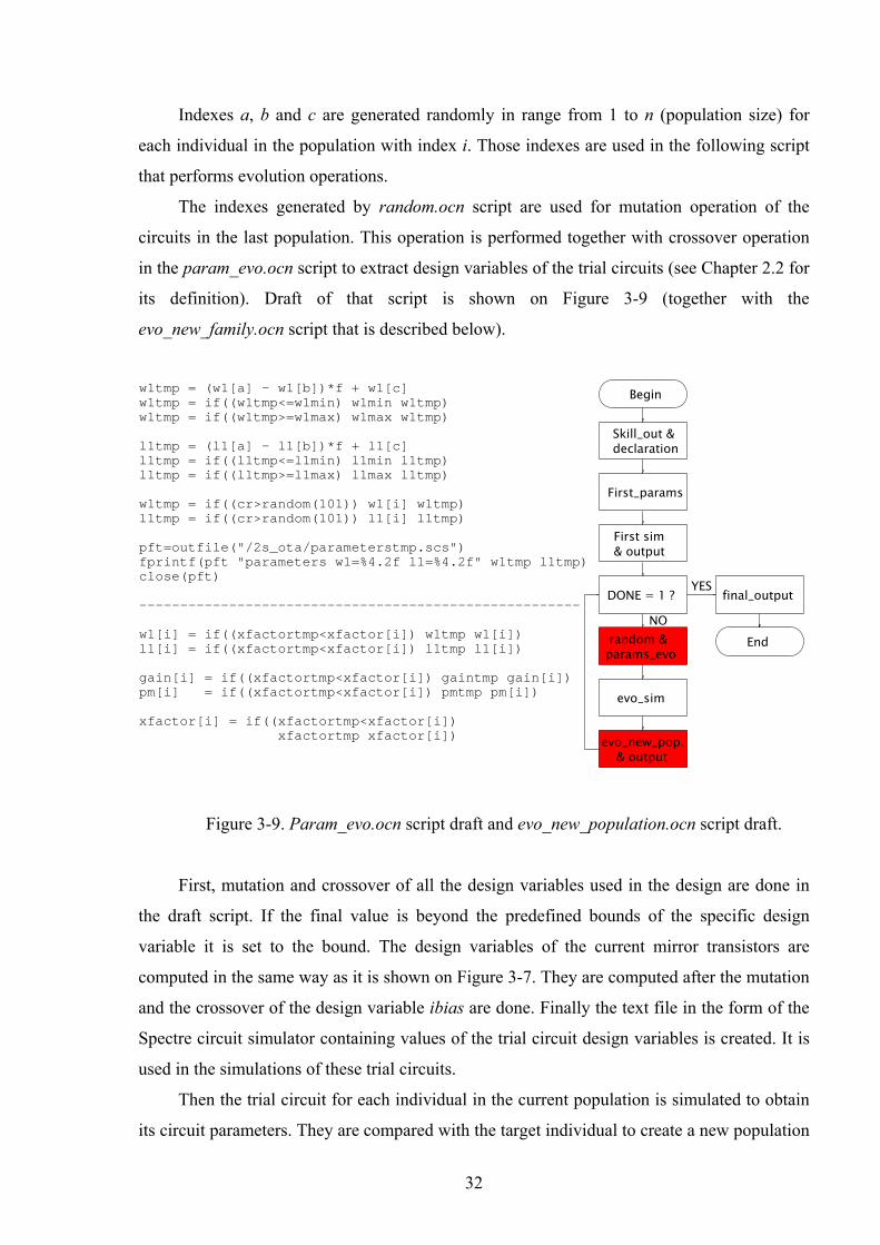
Figure 3-9. Param_evo.ocn script draft and evo_new_population.ocn script draft.
First, mutation and crossover of all the design variables used in the design are done in
the draft script. If the final value is beyond the predefined bounds of the specific design
variable it is set to the bound. The design variables of the current mirror transistors are
computed in the same way as it is shown on Figure 3-7. They are computed after the mutation
and the crossover of the design variable ibias are done. Finally the text file in the form of the
Spectre circuit simulator containing values of the trial circuit design variables is created. It is
used in the simulations of these trial circuits.
Then the trial circuit for each individual in the current population is simulated to obtain
its circuit parameters. They are compared with the target individual to create a new population

33
with the most fitting individuals. The simulations are done in a similar way to the first
population as described above using the first_sim.ocn script shown in Figure 3.8. The script
that takes care of the trial circuits simulations is called evo_sim.ocn. It is not shown here since
it is very similar to the first_sim.ocn one. The changes are following:
• Circuit variables are taken from parameterstmp.scs file created by param_evo.ocn
script (not the parameters_first.scs file as in the first population simulations).
• Simulated circuit parameters and value of the fitness function are saved to the
paramtmp variable (not the param[i] since just one circuit data are needed in time).
Otherwise same circuit test-benches are simulated by this script in the same PVT
corners. Same functions are used to extract the specified circuit parameters.
When all the trial circuits are simulated, new population is created using the script
evo_new_population.ocn script. Its draft is shown on Figure 3-9.
The fitness of each trial individual is compared with the target one. If the fitness of the
trial one is better (lower in my case), the trial individual is taken to the new population.
Otherwise the target individual remains in the new population. There is an example for the
individuals with design variables w1 and l1 and with the circuit parameters gain and pm given
in the draft on Figure 3-9.
After the new population creation the details about the new population are saved to the
output files. New population is searched if it contains an individual that meets the
specification. If not, the process of the evolution is repeated until the solution is found.
Another end conditions are defined by the novel optimization watchdog feature that is
described in Chapter 3.4.
Last step of the optimization core (except of the closing of the output files) is the
final_output.ocn script. Draft of that script is shown in Figure 3-10.
The purpose of that script is to help to modify the OT settings to obtain better circuit in
the next OT run (also with help of the novel optimization watchdog feature – see Chapter 3.4
for its description).
The script works as follows. First, it finds the fittest individual in the last population that
represents the best circuit that was found by the optimization. Then the script checks the
values of its circuit parameters and design variables and put a note to the output files about the
circuit parameters that do not meet the specification and about the design variables that are
equal to the upper or lower limit of those variables.

34
End
Begin
First_params
random ¶ms_evo
First sim & output
DONE = 1 ?YES
NO
evo_sim
Skill_out &declaration
evo_new_pop. & output
final_output
i = 1for(j 1 n for(k 1 n
i = if((F[k]<F[i]) k i)
))
fprintf(of "\nBEST CIRCUIT OPTIMIZED:\n")
load("/2s_ota/output_data.ocn")
if((gain[i]<gainaim) fprintf (of "Gain lower about %3.1f dB\n" gainaim-gain[i])) if((pm[i]<pmaim) fprintf (of "PM lower about %3.1f degrees\n" pmaim-pm[i]))
if((w1[i]<=w1min) fprintf(of "w1 at the bottom limit\n"))if((l1[i]<=l1min) fprintf(of "l1 at the bottom limit\n"))if((w1[i]>=w1max) fprintf(of "w1 at the upper limit\n"))if((l1[i]>=l1max) fprintf(of "l1 at the upper limit\n"))
Figure 3-10. Final_output.ocn script draft.
This information can help in the following decisions and actions:
• If the best optimized circuit does not meet the user’s specification and if some design
variable of this circuit is equal to its bound, better circuit can be reached by the change
of this bound.
• Similarly – if the best optimized circuit meets the specification and some of its design
variable is equal to its bound, better circuit can be reachable by the changing of the
design variables bounds.
• If the design variables bounds can not be changed (for example to make lower bound
of transistor channel length because of a bad transistor matching) and the best
optimized circuit does not meet the specification, the circuit specification relaxing can
be considered.
The optimization core process ends by running the final_output.ocn script. At that point
the optimization process is finished and the output files should be checked. If the optimization
process does not find the task solution, optimization watchdog feature described in Chapter
3.4 can be used to help to optimize to the result that meets its specification.

35
Second part of the final_output.ocn script is shown on Figure 3-12 in Chapter 3.4 about
the optimization watchdog feature. It shows how this novel feature advices how to modify the
search space to shorten optimization time.
3.3 Simulator Interface
Usage of the circuit simulator is needed because the simulation based optimization
approach is used in my OT. The simulation results post-processing tool must be available and
under the control of the OT to be able to extract the specified parameters from the output of
the simulations. The interface between the OT core designed by the Ocean scripting language
and the Spectre circuit simulator is described in this chapter.
The simulator interface is included in the optimization core script, specifically in the
first_sim.ocn script and in the evo_sim.ocn script. Description of those scripts was given in
Chapter 3.2. Detailed description of the simulator interface is listed here. The simulator
interface is shown on Figure 3-11. as it is implemented in my OT.
First, the list of all corners (temperature, voltages, currents and technology corners) that
will be used is defined in variables like TempList and lvList. This is very useful for
performing of PVT simulation and worst case simulations.
This definition is used to create a set of simulations in specific PVT corners using the
foreach function. It means that the simulation, which is described below this function, is done
for each combination of the above mentioned corners.
After that definition the specific simulation is set and run. The Spectre simulator is
chosen as the simulator to be used. The simulation corners defined at the beginning of the
script are used to specify the simulation conditions using the functions like desVar, modelFile
and temp. If different IC technology is used, device models defined by modelFile are simply
changed.
Other design variables are set by the loading of the parameters_first.scs file by the
definitionFile function. This gives the ability to the optimization core to change the simulation
condition when the design variables are changed by the optimization algorithm during the
optimization process.
The test-bench net-list is loaded by design command. This approach makes the OT easy
to modify. The net-list, which is loaded by the simulation interface, can be changed by
Cadence design environment without changing of optimization core script.
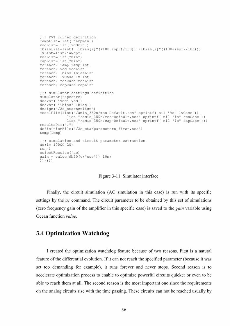
36
;;; PVT corner definitionTempList=list( tempmin )VddList=list( vddmin )IbiasList=list( (ibias[i]*((100-ispr)/100)) (ibias[i]*((100+ispr)/100)))lvList=list("awcp")resList=list("min")capList=list("min")foreach( Temp TempListforeach( Vdd VddListforeach( Ibias IbiasListforeach( lvCase lvListforeach( resCase resListforeach( capCase capList
;;; simulator settings definitionsimulator('spectre)desVar( "vdd" Vdd )desVar( "ibias" Ibias )design("/2s_ota/netlist")modelFile(list("/amis_350n/mos-Default.scs" sprintf( nil "%s" lvCase ))
list("/amis_350n/res-Default.scs" sprintf( nil "%s" resCase )) list("/amis_350n/cap-Default.scs" sprintf( nil "%s" capCase )))
resultsDir(".")definitionFile("/2s_ota/parameters_first.scs")temp(Temp)
;;; simulation and circuit parameter extractionac(1m 1000G 20)run()selectResults('ac)gain = value(db20(v("out")) 10m)))))))
Figure 3-11. Simulator interface.
Finally, the circuit simulation (AC simulation in this case) is run with its specific
settings by the ac command. The circuit parameter to be obtained by this set of simulations
(zero frequency gain of the amplifier in this specific case) is saved to the gain variable using
Ocean function value.
3.4 Optimization Watchdog
I created the optimization watchdog feature because of two reasons. First is a natural
feature of the differential evolution. If it can not reach the specified parameter (because it was
set too demanding for example), it runs forever and never stops. Second reason is to
accelerate optimization process to enable to optimize powerful circuits quicker or even to be
able to reach them at all. The second reason is the most important one since the requirements
on the analog circuits rise with the time passing. These circuits can not be reached usually by

37
the standard optimization methods. They require advanced approaches like the novel
optimization watchdog feature.
The optimization watchdog feature introduces additional final condition to the
differential evolution algorithm. The first natural final condition is the occurrence of an
individual with fitness function equal to zero. It is the circuit that meets the user specification.
That is the goal of the optimization.
The final condition introduced by the optimization watchdog feature is the occurrence of
predefined number of populations (parameter WDP) in a row without significant progress of
the optimization (defined by specific difference between fitness of the trial and target circuit –
parameter WDD). This indicates that the optimization is not able to get much better (specified
by the WDD parameter) circuit in reasonable time (defined by the WDP parameter). It is
implemented as follows:
otherwiseWDWDWDtFtFniWD
CC
DiiC
1)()1( ,...,1for 0
+=−≤+=∃=
(3-1)
Where WDC, WDD and WDP are special watchdog variables, n is the number of
individuals in one population. The optimization ends without satisfying the specification if
WDC is equal to WDP.
WDD and WDP parameters are set to their default values by the OT. On the other hand
the setting can be changed by the tool user. WDC variable is evaluated during the optimization
process by the tool as shown on Figure 3-6.
The implementation of the (3-1) in the optimization core can be seen on the Figure 3-6.
which is the top script of the OT core. The variable done signalizes the optimization end. It is
controlled not only by the fitness of the individuals in the population but also by the
optimization watchdog.
The optimization watchdog feature can be used (not only) in following cases and with
following settings:
• First of all the optimization watchdog feature was implemented to fix the differential
evolution disadvantage. Its optimization process can never stop if the specification is
set too demanding for given design variables bounds. This feature is corrected if the
optimization watchdog is just used. WDD shall be set rational positive and WDP also
positive but whole.

38
• Optimization watchdog can be used for the first impression with the circuit, its
abilities and parameters. The settings of the optimization watchdog ensure that the
optimization ends if the first symptom of the optimization stuck occurs. It results in
quick optimization time and optimized circuits that most probably do not meet the
specification but their parameters values are close to those that can be expected from
the chosen type of the circuit. The optimization watchdog should be close to the
following one: WDD = 0.05 to 0.2 (lower value is proposed for more complicated
circuits) and WDP = 1. Also the ranges of the design variables shall be set as wide as
possible to not limit the circuit by the design variables limits.
• The setting for the classical optimization is to give the OT some reasonable time to
find the circuit that meets the user’s specification but to stop it when the progress of
the optimization is too slow. The proposed setting of the optimization watchdog
parameters is: WDD = 0.01 to 0.05 (lower value is proposed for more complicated
circuits) and WDP = 5. Again the parameter values should be adjusted depending on
the complexity of the optimized circuit.
• The novel approach to optimize powerful circuits in shorter time is performed in two
steps. The optimization watchdog setting for the first step is: WDD = 0.05 to 0.2 (lower
value is proposed for more complicated circuits), WDP = 1 and using wide ranges of
the design variables for short optimization that examines the circuit, specification set
for the circuit and the limits of the optimization variables quickly. The OT does not
get to the solution but find the part of the design space where the solution can be
found. Then the design variables limits are changed in accordance with that part of the
design space. The setting for the second step is: WDD = 0.01 to 0.05 (lower value is
proposed for more complicated circuits) and WDP = 5 for precise optimization that has
faster progress since the design space is smaller. Thus the OT can achieve powerful
circuit in shorter time.
• There can be also the situation that designer of the circuit realizes after first short
optimization that his specification is beyond the limit of the circuit. Thus he can
change his specification for example by some tradeoff between consumption and slew-
rate of the circuit. Practical demonstration of the optimization watchdog feature with
the results that prove the power of this novel optimization approach is listed in the
Chapter 4.5.

39
WDP can be set also higher in every case if the circuit is more complicated. The WDD
should be set lower and WDP higher if the specification of the optimized circuits is more
challenging.
The simplified Ocean script that recommends how to modify the design variables
bounds is shown on Figure 3-12. The script is a part of the final_output.ocn script listed in
Chapter 3-2.
m = n - 1Ftmp=F[1]for(i 1 m
for(j 1 mwhile((F[j+1]<F[j])
Ftmp=F[j]F[j]=F[j+1]F[j+1]=Ftmp
w1tmp=w1[j]w1[j]=w1[j+1]w1[j+1]=w1tmp
)))
if((mod(n 2)>0) m=((n-1)/2) m=(n/2))
w1min_new = w1[1]w1max_new = w1[1]
for(i 2 mif((w1[i]<w1min_new) w1min_new=w1[i])if((w1[i]>w1max_new) w1max_new=w1[i]))
Figure 3-12. Ocean script – design variables bounds modification.
First, individuals in the final population are sorted from the best one to the worst one.
Then m variable is counted. It specifies the number of the best circuits taken into account in
the bounds modification. I chose m to be 50 % of n (rounded down). It is a tradeoff between
optimization optimality in terms of convergence to the local minimum danger and the
optimization acceleration. The last step of the script creates new bounds of the design
variables. Figure 3-16 shows an example with only one design variable w1.
40
4 Design Examples
This chapter describes implementation of the several analog circuit architectures to the
OT in details. The purpose of this implementation is the possibility to optimize these circuits
in accordance with the input specification in the proposed OT. These circuits optimization has
very short set-up time and are optimized using full PVT simulations. Therefore the resulting
circuits are robust and usually ready for layout. I created novel optimization watchdog feature
(verified in this chapter) that can be used to optimize circuits in shorter time. The proposed
OT can be conveniently extended to be able to optimize a generic circuit in whatever
technology. Details about these possibilities are listed in this chapter. The comparison with
the works published recently is listed here. Following topics are contained in this chapter:
• The implementation of several design examples to the OT to be able to optimize them
using my OT. Design of the schematics of those design examples. Test-benches
creation for the design examples needed to extract the optimized circuit parameters.
That, among others, ensures a very short setup time of my OT and provides reusability
of the design examples. The design examples I implemented are:
o Two-stage Miller OTA that is described in Chapter 4.1. This design example
was chosen to test and debug my OT. It is suitable to compare the proposed
OT with other works since it is used in lot of works published so far.
o Folded cascode OTA that is described in Chapter 4.2. This circuit was chosen
to enable the optimization of different OTA architecture to choose better
architecture for the specific application and circuit specification.
o Voltage regulator that is described in Chapter 4.3. The optimization of this
circuit is the main scope of my thesis.
• Full PVT simulations of each design example in every corner for every optimized
circuit parameter. Determination of the worst case corner for each optimized circuit
parameter. Running of the simulation in the worst case corner improves greatly the
optimization time.
• Possible optimization of an arbitrary circuit. All steps needed to implement a generic
circuit to my OT are listed in Chapter 4.4.
• Verification of the novel Optimization Watchdog feature. Example showing how the
Optimization Watchdog feature can speed up the optimization more than two times.

41
• Comparison with other works is given in Chapter 4.6. The comparisons show that my
OT is up-to-date and is usable in present days for everyday design of the analog ICs.
All the design examples mentioned in this chapter use AMIS 0.35 μm CMOS
technology device models. A test-chip to verify my OT by manufactured chip measurements
was designed in that technology. More details about this test-chip design, layout and
measurement are listed in Chapter 5. My OT can work with any other technology. It is just
needed to change conveniently the references to the technology models in the first_sim.ocn
and evo_sim.ocn scripts of the OT core described in Chapter 3. and Figure 3-9. If the model
corners have different names in the different technology it is needed to change their names in
these scripts as well.
All circuits were designed for temperature range from -10 °C to 50 °C, supply (input)
voltage range from 1.8 V to 2.0 V and with bias current variations of ± 30%. The
optimizations were running on the machine using 2.5 GHz two core Intel processor with 4 GB
RAM.
Population size n was chosen to 15 individuals for all optimized circuits. It was proven
to be large enough for the optimization convergence and on the other hand small enough for
the optimization speed. Scaling factor SF was set to 0.8 and crossover constant CR to 0.7 for
all optimizations. These values were found as a good compromise between the optimization
convergence speed and the possibility to obtain powerful circuits.
Accurate approach to size the current mirror transistors was used for all design
examples. It is based on using the same width and length of all current mirror transistors.
Multiple transistors in parallel are used to increase or decrease bias current in the specific
branch of the circuit. It is much better transistor matching approach than to size widths and
lengths of the current mirror transistor independently as in [16][17][24][25][26].
The width and length of the current mirror transistors are not optimized (they are not
design variables). They are set to be in correct mode in accordance with the bias current that
is optimized. It is done by “rule of thumb” used in analog circuit design:
mVVV THGS 100+≥ (4-1)
Where VGS is gate-source voltage of the current mirror transistor and VTH is its threshold
voltage. This rule must be fulfilled for all PVT corners.

42
I used a look-up table for setting correct dimensions of the current mirror transistors. I
simulated width and length of the transistors to have correct operation point (to be in the
strong inversion). The simulation details are listed in Table 4-1. for various bias currents and
for PMOS and NMOS transistors.
NMOS PMOS Current
IB (μA) W (μm) L (μm) W/L/IB
(μA-1) W (μm) L (μm)
W/L/IB
(μA-1)
0.1 1.0 16.5 0.61 0.5 1.6 3.13
0.2 1.0 8.5 0.59 1.0 1.6 3.13
0.5 1.0 3.5 0.57 1.4 1.0 2.80
1.0 1.0 2.0 0.50 2.7 1.0 2.70
1.5 1.0 1.4 0.48 3.9 1.0 2.60
2.0 0.9 1.0 0.45 5.0 1.0 2.50
3.0 1.3 1.0 0.43 7.3 1.0 2.43
5.0 2.0 1.0 0.40 12.0 1.0 2.40
10.0 4.0 1.0 0.40 10.2 0.5 2.04
20.0 8.0 1.0 0.40 20.0 0.5 2.00
Table 4-1. W/L of the current mirror transistors for correct operation point.
The dimensions of the transistors are finally sized in accordance with the following rules
and to bias current. Those rules for NMOS transistor are used in first_params.ocn script
shown on Figure 3.9 in Chapter 3.2. First W/L of the transistors is computed in accordance
with the bias current IB:
W/L of the NMOS transistor is:
• If (IB > 3 μA) then (W/L = (IB * 1e6) / 2.4).
• If (3 μA ≥ IB > 1.5 μA) then (W/L = (IB * 1e6) / 2.2).
• If (IB ≤ 1.5 μA) then (W/L = (IB * 1e6) / 2.05).
W/L of the PMOS transistor is:
• If (IB > 5 μA) then (W/L = (IB * 1e6)*2.7).
• If (5 μA ≥ IB > 1.5 μA) then (W/L = (IB * 1e6) * 2.3).

43
• If (IB ≤ 1.5 μA) then (W/L = (IB * 1e6) * 2.1).
The generation of width W and length L of the current mirror transistor is the same for
NMOS and PMOS transistors. W and L are derived in the way to ensure minimum transistor
area of 2 μm2:
For W/L > 0.96:
• If (W/L > 8) then (L = 0.55 μm).
• If (8 ≥ W/L > 4) then (L = 0.8 μm).
• If (4 ≥ W/L > 2) then (L = 1.1 μm).
• If (W/L ≤ 2) then (L = 1.6 μm).
• W = W/L * L μm.
For W/L ≤ 0.96:
• If (W/L < 0.06) then (W = 0.4 μm).
• If (0.06 ≤ W/L < 0.12) then (W = 0.55 μm).
• If (0.12 ≤ W/L < 0.24) then (W = 0.8 μm).
• If (0.24 ≤ W/L < 0.48) then (W = 1.1 μm).
• If (W/L ≥ 0.48) then (W = 1.55 μm).
• L = W / W/L μm.
W and L of the PMOS and NMOS current mirror transistors are shown on Figure 4-1.
for various bias currents. Values for current higher than 20 μA and lower than 0.1 μA are
extrapolated. The dimensions generation is not very sophisticated but simple and well
working.
All design examples were designed using PVT simulations. All technology, voltage,
current and temperature corners were taken into account. Circuit parameter values in the
worst case corner are taken into account in the fitness function derivation for each individual
in each population. It is needed to produce robust circuits. Those circuits are usually ready to
use without any need of another verifications and schematic changes.
The drawback of this approach is much longer time of the optimizations process. If 5
corners are taken into account the optimization time is 32 times longer (considering that the
most of the optimization time is taken by the circuit simulations). I solved this issue by
simulating several random circuits to identify the worst case corner(s) for each circuit
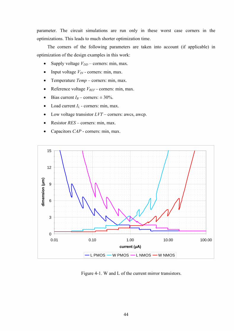
44
parameter. The circuit simulations are run only in these worst case corners in the
optimizations. This leads to much shorter optimization time.
The corners of the following parameters are taken into account (if applicable) in
optimization of the design examples in this work:
• Supply voltage VDD – corners: min, max.
• Input voltage VIN - corners: min, max.
• Temperature Temp – corners: min, max.
• Reference voltage VREF - corners: min, max.
• Bias current IB – corners: ± 30%.
• Load current IL - corners: min, max.
• Low voltage transistor LVT – corners: awcs, awcp.
• Resistor RES – corners: min, max.
• Capacitors CAP - corners: min, max.
0
3
6
9
12
15
0.01 0.10 1.00 10.00 100.00
current (μA)
dim
ensi
on (μ
m)
L PMOS W PMOS L NMOS W NMOS
Figure 4-1. W and L of the current mirror transistors.

45
4.1 Two-Stage Miller OTA
Circuit schematic of the design example is shown on Figure 4-2. with design variables
highlighted in red. Width and length of the transistors M1, M2 and M3 (parameters W1 and
L1) are not strictly optimized but derived from the bias current by the novel approach. The
current flowing through branches of transistors M2 and M3 are optimized by design variables
M1 and M2. These variables specify the number of transistors in parallel. The number of
design variables is 11. Load of the OTA was chosen to be purely capacitive (10 pF).
vdd
vss
inn inp out
biasIb
M1M2M3
M4 M5
M6 M7
M8
R1
C1
W1L1
W1L1M2
W1L1M1
W2L2
W2L2
W3L3
W3L3
W4L4
R
C
out_n
Figure 4-2. Two-stage Miller OTA.
I optimized following circuit parameters of this design example:
• Zero frequency voltage gain – A0.
• Unity gain bandwidth – GBW.
• Phase margin – PM.
• Slew rate – SR
• Current consumption – IDD.

46
I have designed two test-benches of the circuit to extract these circuit parameters. First
one was designed to simulate SR and IDD and second one to simulate A0, GBW and PM.
The first test-bench is shown on Figure 4-3. to explain how they are created. Transient
simulation of this test-bench is performed in the optimization process. The circuit contains the
design example, its capacitive load Cload, Vdd supply voltage source, Vdd/2 reference voltage
source and Ib bias current source. The voltage source that generates voltage at inp node has
pulse behavior. It switches the inp node from vss to vdd in one time and from vdd to vss in
another one. Thus rising and falling slew-rate can be simulated. The worse one of them is
taken into account during the fitness function evaluation. The static consumption is computed
for two cases. The first one is derived when the inp node is at vdd and second one when the
inp node is at vss. The worse value is used to compute circuit fitness.
inn
out+
-
inp
Ib
Vdd/2Vdd
vdd
vss
Cload
two-stage OTA
Figure 4-3. Test-bench for slew-rate and current consumption simulations.
The second test-bench is very similar and also very simple. From that reason its
description is not given in this thesis. I created net-lists of those test-benches. Links to those
net-lists are used in first_sim.ocn (Figure 3-9) and evo_sim.ocn scripts of the optimization
core described in Chapter 3.2. Simulations of the created test-benches are performed via these
links thus the test-benches to be simulated can be conveniently modified if needed.
The worst case corners of the optimized circuit parameters are summarized in Table 4-2.
Their determination was the last step of the design example implementation.

47
Parameter Temp VDD IB LVT RES CAP
A0 Min Min ± 30% awcp Min Min
PM Min Max + 30% Awcp/awcs Min Min
GBW Max Min - 30% Awcs Max Max
SR Min Min - 30% Awcp/awcs Max Max
IDD max max + 30% Awcs Max Min
Table 4-2. Circuit parameter worst case corners of the two-stage Miller OTA.
Parameter A0 (dB) PM (°) GBW (MHz) SR (V/μs) IDD (μA)
Specification 70.0 60.0 1.00 0.50 50.0
Result 89.6 62.8 1.65 1.05 48.8
Table 4-3. Circuit parameters - two-stage Miller OTA.
Variable Lower bound Upper bound Result
W1 (μm) N/A N/A 3.35
L1 (μm) N/A N/A 1.1
W2 (μm) 1.0 50 43.0
L2 (μm) 0.5 5 3.0
W3 (μm) 1.0 10 10.0
L3 (μm) 1.0 10 9.6
W4 (μm) 5.0 50 47.1
L4 (μm) 0.5 5 0.5
R (kΩ) 0.1 10 6.04
C (pF) 0.1 10 4.21
M1 (-) 1 10 1
M2 (-) 1 10 4
Ib (μA) 0.1 30 7.27
Table 4-4. Optimization variables – two-stage Miller OTA.

48
The first_sim.ocn script was modified to simulate all corners, identify the worst case
corners and to create output text file containing results of those simulation. I run the script for
several randomly created circuits and chose the worst case corners. The worst case corner can
change for different sizing of the circuit. Therefore several corners are specified for some
circuit parameters.
I performed the optimization with the specification shown in Table 4-3. The WDP
optimization watchdog variable was set to 5 and WDD variable to 0.05. The setting of the
design variables for the optimization is shown in Table 4-4.
The optimization time was 4 hours and 10 minutes (solution was found in the 21st
population). The circuit parameters of the resulting circuit are listed in Table 4-3.
Optimization variables of the found solution are in Table 4-4.
4.2 Folded Cascode OTA
Circuit schematic of the design example is shown on Figure 4-4. with design variables
highlighted in red.
vdd
vss
inninpout
Ib
M1M2M4M5
M9 M10
M6
W1L1
W3L3
bias
W1L1
W1L1
W1L1M
W1L1M
W2L2M
W2L2
W2L2
W3L3
W4L4
W4L4
W5L5
W5L5
W6L6
W6L6
W7L7
W7L7
W8L8
W8L8
M7M8 M11 M12
M15 M16
M14M13
M3
M18
M17
M19
M20
Figure 4-4. Folded cascode OTA.
Width and length of the transistors M1, M2, M3, M4, M5, M6, M7 and M8 (parameters
W1, L1, W2 and L2) are not strictly optimized but derived from the bias current by novel
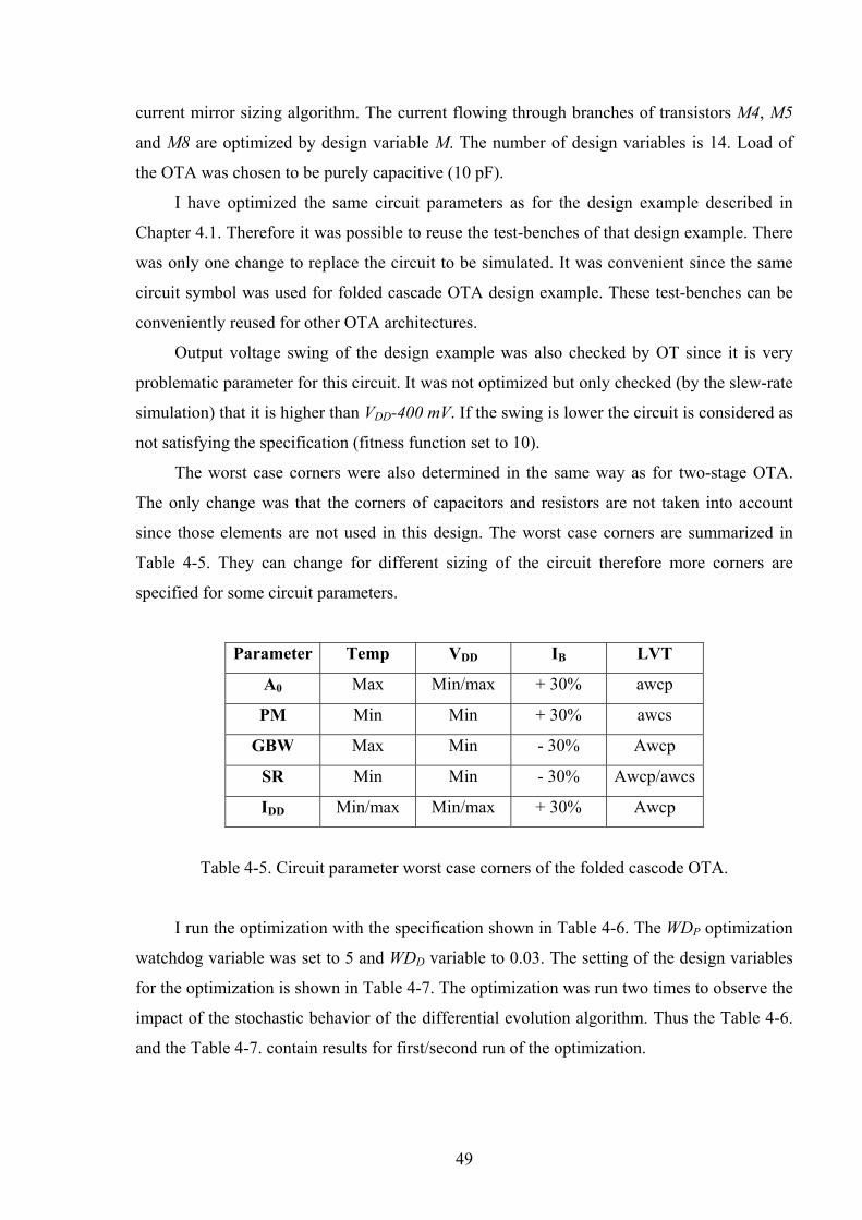
49
current mirror sizing algorithm. The current flowing through branches of transistors M4, M5
and M8 are optimized by design variable M. The number of design variables is 14. Load of
the OTA was chosen to be purely capacitive (10 pF).
I have optimized the same circuit parameters as for the design example described in
Chapter 4.1. Therefore it was possible to reuse the test-benches of that design example. There
was only one change to replace the circuit to be simulated. It was convenient since the same
circuit symbol was used for folded cascade OTA design example. These test-benches can be
conveniently reused for other OTA architectures.
Output voltage swing of the design example was also checked by OT since it is very
problematic parameter for this circuit. It was not optimized but only checked (by the slew-rate
simulation) that it is higher than VDD-400 mV. If the swing is lower the circuit is considered as
not satisfying the specification (fitness function set to 10).
The worst case corners were also determined in the same way as for two-stage OTA.
The only change was that the corners of capacitors and resistors are not taken into account
since those elements are not used in this design. The worst case corners are summarized in
Table 4-5. They can change for different sizing of the circuit therefore more corners are
specified for some circuit parameters.
Parameter Temp VDD IB LVT
A0 Max Min/max + 30% awcp
PM Min Min + 30% awcs
GBW Max Min - 30% Awcp
SR Min Min - 30% Awcp/awcs
IDD Min/max Min/max + 30% Awcp
Table 4-5. Circuit parameter worst case corners of the folded cascode OTA.
I run the optimization with the specification shown in Table 4-6. The WDP optimization
watchdog variable was set to 5 and WDD variable to 0.03. The setting of the design variables
for the optimization is shown in Table 4-7. The optimization was run two times to observe the
impact of the stochastic behavior of the differential evolution algorithm. Thus the Table 4-6.
and the Table 4-7. contain results for first/second run of the optimization.

50
Parameter A0 (dB) PM (°) GBW (MHz) SR (V/μs) IDD (μA)
Specification 50 60 0.5 0.2 50
Result 68.0 / 66.3 86.5 / 87.9 0.58 / 0.64 0.21 / 0.30 35.8 / 32.7
Table 4-6. Circuit parameters - folded cascade OTA.
Variable Lower bound Upper bound Result
W1 (μm) N/A N/A 2.9 / 3.0
L1 (μm) N/A N/A 1.1 / 1.6
W2 (μm) N/A N/A 7.4 / 5.6
L2 (μm) N/A N/A 0.55 / 0.8
W3 (μm) 1.0 50 28.4 / 22.1
L3 (μm) 0.5 5 1.1 / 2.6
W4 (μm) 1.0 20 19.7 / 14.2
L4 (μm) 1.0 20 6.9 / 7.3
W5 (μm) 0.5 50 7.4 / 16.2
L5 (μm) 0.5 50 17.6 / 4.8
W6 (μm) 0.5 50 6.5 / 29.3
L6 (μm) 0.5 50 3.4 / 5.6
W7 (μm) 0.5 50 1.3 / 1.5
L7 (μm) 0.5 50 22.8 / 3.6
W8 (μm) 0.5 50 2.9 / 4.2
L8 (μm) 0.5 50 10.2 / 46.8
M (-) 1 9 1 / 3
Ib (μA) 0.1 20 17.0 / 3.0
Table 4-7. Design variables – folded cascade OTA.
The optimization time was 2 hours and 2 minutes (solution was found in the 16th
population) for the first run and 10 minutes for the second run. Solution of the second run was
found in the first population thus no evolution of the individuals was needed. This is just a
good luck that the solution was chosen by the random generation of the individuals in the first
population. It would be not so easy for more demanding circuit. The part of the design space
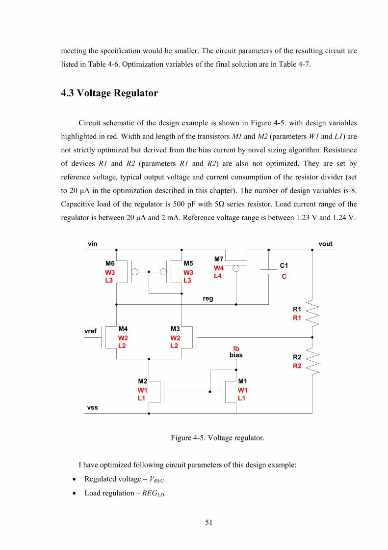
51
meeting the specification would be smaller. The circuit parameters of the resulting circuit are
listed in Table 4-6. Optimization variables of the final solution are in Table 4-7.
4.3 Voltage Regulator
Circuit schematic of the design example is shown in Figure 4-5. with design variables
highlighted in red. Width and length of the transistors M1 and M2 (parameters W1 and L1) are
not strictly optimized but derived from the bias current by novel sizing algorithm. Resistance
of devices R1 and R2 (parameters R1 and R2) are also not optimized. They are set by
reference voltage, typical output voltage and current consumption of the resistor divider (set
to 20 μA in the optimization described in this chapter). The number of design variables is 8.
Capacitive load of the regulator is 500 pF with 5Ω series resistor. Load current range of the
regulator is between 20 μA and 2 mA. Reference voltage range is between 1.23 V and 1.24 V.
vin
vss
vref
biasIb
M1M2
M4 M3
M6 M5 M7C1
W1L1
W1L1
W2L2
W2L2
W3L3
W3L3
W4L4 C
vout
R1R1
R2R2
reg
Figure 4-5. Voltage regulator.
I have optimized following circuit parameters of this design example:
• Regulated voltage – VREG.
• Load regulation – REGLD.

52
• Line regulation – REGLN.
• Temperature drift – DTMP.
• Power supply rejection ration at the frequency of 50 Hz – PSRR50.
• Phase margin – PM.
• Bandwidth – BW.
• Current consumption – IDD.
I have designed five test-benches of the voltage regulator to extract above mentioned
circuit parameters:
• Simple one to simulate VREG, DTMP and IDD. The test-bench consist of the voltage
regulator, load capacitance and DC sources to create the load current and to bias input
voltage and reference voltage. Other test-benches were created as a modification o this
one.
• The source to create load current was modified in the test-bench to extract REGLD. The
source was replaced by the source that changes the load in time. It would be possible
to extract the REGLD from results of two simulations using first test-bench (for
minimum and maxim load). On the other hand it would last longer than one simulation
using this special test-bench.
• The input voltage source was modified in the test-bench to simulate REGLN. The
source was replaced by the source that changes the input voltage in time.
• The feedback loop in the voltage regulator (created by devices R1, M3, M5, M6 and
M7) was divided in the test-bench to extract PM and BW. AC-killer circuit was used to
observe AC characteristics of the feedback loop.
• The input voltage source was modified in the test-bench to simulate PSRR50. The
source with AC component was used to observe behavior of the regulated voltage in
dependence to the noisy input voltage.
I created net-lists of those test-benches and use them in the same way as in the previous
design example cases (links to those net-lists are used in first_sim.ocn and evo_sim.ocn of the
optimization core). The worst case corners were determined in the same way as in previous
design examples using modified first_sim.ocn script. The resulting worst case corners are
summarized in Table 4-8.

53
Parameter Temp VREF VIN IB IL LVT RES CAP
VREG Max Min Min - 30% Max Awcs Max Min
REGLD Max Max Min - 30% N/A Awcps Min Min
REGLN Max Max N/A - 30% Max Awcs Min Min
DTMP N/A Min Min + 30% Min Awcp Max Max
PSRR50 Max Max Min - 30% Max Awcs Min Min
PM Max Min Max + 30% Min Awcs Max Max
BW Max Max Min + 30% Min Awcp Max Max
IDD Min Max Max + 30% Min Awcp Min Max
Table 4-8. Circuit parameter worst case corners of the voltage regulator.
The setting of the design variables for the optimization is shown in Table 4-9. I run the
optimization with the specification shown in Table 4-10. The WDP optimization watchdog
variable was set to 3 and WDD variable to 0.05.
Variable Lower bound Upper bound Result
W1 (μm) 0.4 50 0.4
L1 (μm) 0.55 50 8.2
W2 (μm) 1.0 20 12.2
L2 (μm) 1.0 20 10.2
W3 (μm) 1.0 20 18.7
L3 (μm) 1.0 20 10.2
W4 (μm) 250 500 434.8
L4 (μm) 0.5 1 0.5
C (pF) 0.1 5 0.85
R1 (kΩ ) N/A N/A 13.25
R2 (kΩ) N/A N/A 61.75
Ib (μA) 0.1 10 0.1
Table 4-9. Design variables – voltage regulator.

54
The circuit parameters of the resulting circuit are listed in Table 4-10. Optimization
variables of the final solution are in Table 4-9. Lower and upper bounds of design variables
R1 and R2 are not needed. Their values depend just on the circuit specification (reference
voltage, output voltage and current consumption of the resistor divider).
Parameter VREG (V) REGLN (mV). REGLD (mV) DTMP (mV/°C)
Specification 1.5±0.05 30 30 0.5
Result 1.5±0.008 0.4 1.2 0.003
Parameter PM (°) BW (kHz) PSRR50 (dB) IDD (μA)
Specification 60 150 40 50
Result 91.3 171 51.6 37.1
Table 4-10. Circuit parameters – voltage regulator.
Optimization time was 48 minutes (solution was found in the 5th population).
Optimization had very good progress since the number of optimization parameters is low
despite the high number of optimized circuit parameters.
4.4 New Design Example
It is possible to extend the proposed OT to an arbitrary circuit. This chapter summarized
the actions needed to extend my tool to be able to optimize other kinds of analog circuits. The
following points must be fulfilled:
• Creation of the new design example schematic and symbol. Parameters of the circuit
devices must be equal to the names of the design variables to be used in the
optimization process.
• Creations of the circuit test-benches and their net-lists for the new design example.
Every circuit parameter to be optimized must be extractable from the simulation
results of those test-benches. Creation of the test-benches must not be done if a same
design example is implemented in the tool. If different architecture of OTA or voltage
regulator is needed, test-benches from the implemented design examples can be
reused.

55
• Definition of the circuit parameter extracts. Creation of the extract must not be done if
a same design example is implemented in the tool.
• Definition of the design variables. The design variables used in the new design
example schematic must be defined in the tool core script.
• Determination of the circuit parameters worst cases (optional to speed up the circuit
optimization).
• New toolbar item in the OT interface. The toolbar shall be extended by the
modification of the user interface scripts described in Chapter 3.1.
4.5 Optimization Watchdog Verification
The verification of the novel optimization watchdog feature contribution is given in this
chapter. The purpose of this verification is to show that the reduction of the design space
described in Chapter 3.4 (optimization watchdog feature details) can speed up the
optimization process. The two-stage OTA design example is used for the watchdog
verification.
Demanding specification of the circuit was used. The optimization watchdog parameters
WDP and WDD were set to 1 and 0.1 respectively for the first rough optimization. The bounds
of the design variables were updated in accordance with the result of the first optimization (to
cover all values from the best half of the individuals in the last population). The second
optimization using reduced search space was run with watchdog parameter WDP and WDD set
to 5 and 0.03 respectively. Parameter WDP was set to 5 and parameter WDD to 0.01 for the
optimization without using of the watchdog.
Table 4-11. contains circuit specification, optimization results with and without using of
the optimization watchdog.
The time of the first watchdog optimization was 120 minutes (optimization lasted 10
populations). The second watchdog optimization lasted 276 minutes. Thus the complete
optimization time was 396 minutes (solution was found in the 23rd population) with using of
the watchdog. The optimization time was 960 minutes (solution was found in the 80th
population) without using of the watchdog. Thus the optimization time was reduced more
than two times. Design variables with their bounds before/after the reduction of the search
space and optimization results values are in Table 4-12.

56
Parameter A0 (dB) PM (°) GBW (MHz) SR (V/μs) IDD (μA)
Specification 90 60 2.0 2.0 20
Result - WD 90 64 2.8 2.3 16
Result - WD 94 60 2.4 2.2 13
Table 4-11. Circuit parameters - two-stage Miller OTA.
Variable Lower bound Upper bound Result - WD Result - WD
W1 (μm) 0.4 50 2.6 1.6
L1 (μm) 0.55 50 1.6 2.7
W2 (μm) 0.5/10 50 37.2 50.0
L2 (μm) 0.5 20 1.7 5.5
W3 (μm) 0.5/8 50 41.0 18.1
L3 (μm) 0.5/13 50 49.4 50.0
W4 (μm) 0.5/9 50 38.4 46.5
L4 (μm) 0.5 10/7 0.7 0.5
R (k Ω ) 0.1 10 0.1 0.1
C (pF) 0.1 10/5 0.58 0.38
M1 (-) 1 10 1 2
M2 (-) 1 10 2 6
Ib μA 0.1 30/9 4.0 1.2
Table 4-12. Design variables – two-stage Miller OTA.
Large differences between two optimized circuits are apparent. The reason of these
differences can be seen in presence of more solutions for one specification (see Chapter 4.6
for more details).
4.6 Comparison with Other Works
The comparison of my OT with other optimization approaches presented so far is given
in this chapter. I used two-stage Miller OTA design example to perform the comparisons
since it is the most frequently used design example in the papers published recently.

57
The comparison was a difficult task since not all details needed to compare fully the
results were presented for example in works [13][16][17][24][25][26]. Those important
details are:
• Bounds of the design variables. An optimization with wider variable ranges takes
generally longer time.
• Time of the optimization task. This is the main criterion to compare the optimization
approaches. The only way to compare the tools without its value is to find if my tool is
able to achieve same results.
• Supply voltage of the OTA.
• Bias current of the design example.
• Capacitive load of the optimized circuit.
The proposed OT was compared with works [13][16][17]. These works present results
with inaccurate current mirrors in term of matching. My solutions use more accurate approach
of the mirrors sizing described in Chapter 4. Thus resulting circuits of my optimizations are
accurate in comparison with the works [13][16][17] even if the typical circuit parameters are
the same.
First, the comparison with work [13] is given. This article consists of comparison of
various optimization algorithms. I compared my OT with the result of the most similar
optimization algorithm given in [13]. On the other hand the comparison was not easy since
there is not mentioned value of the load capacitance of the sized circuit in [13]. I chose load
capacitance of 1 pF. WDD was set to 0.05 and WDP to 5. Supply voltage of the circuit is 2 V.
The circuit specification and resulting circuit parameters are listed in Table 4-13. Table 4-14
contains bounds and resulting values of the design variables.
Parameter A0 (dB) PM (°) GBW (MHz) SR (V/μs) IDD (μA)
Specification 70 60 1.0 1.0 75
Result 1 86 68 2.5 1.0 42
Result 2 86 66 3.3 1.7 28
Result - [13] 92 63 1.7 1.0 70
Table 4-13. Circuit parameters – comparison with [13].

58
Tables 4-13 and 4-14 contain two different optimization results found for the same
conditions by my OT. Stochastic behavior of the optimization algorithm is apparent from
difference of these solutions. It also explains the reason why my solutions are different from
the one presented in [13]. Another reason is that the specification is not a global optimum of
the optimization task. Thus more different solutions exist for the given specification.
Variable Lower limit Upper limit My Results 1/2 Result [13]
W1 (μm) 5 20 2.8/2.4 17.0
W2 (μm) 50 150 84.5/65.6 71.4
W3 (μm) 5 20 12.3/8.2 12.6
W4 (μm) 50 250 158.6/186.2 141.5
C (pF) 0.1 10/5 3.7/2.0 2.6
M2 (-) 1 10 4/4 N/A
Ib μA 1 20 6.15/5.27 2.03
Table 4-14. Design variables – comparison with [13].
Work [13] uses SF = 0.5, CR = 0.8 and n = 30. Lengths of the transistors are not swept
and are set to 1 μm. Resistance R1 is not used (thus it is set to 0 Ω in my optimization).
Transistors M1 and M2 has the same size, transistor M3 has higher W and the same L that can
lead to inaccurate current mirroring. I solved it by setting variable M1 to 1 and to sweep
variable M2 in my optimization.
The differences between [13] and my optimization are that CMRR is optimized to 90 dB
and typical simulations only are run in [13]. I do not optimize CMRR (Common Mode
Rejection Ratio) but use PVT simulation to obtain my result. The results in Table 4-12 are
typical results in comparison with my worst case results. Corners were set equal to those
mentioned in Chapter 4.1.
Optimization time of [13] was 32 minutes and my one 51 and 63 minutes (solution
found in 5th and 6th population) that is a very good result for optimization using PVT
simulations.
Second comparison was done with work [16]. It presents optimization approach based
on adaptive genetic algorithm. The comparison was not easy since [16] does not contain
information about bias current of the circuit. 3dB frequency and noise is optimized in addition
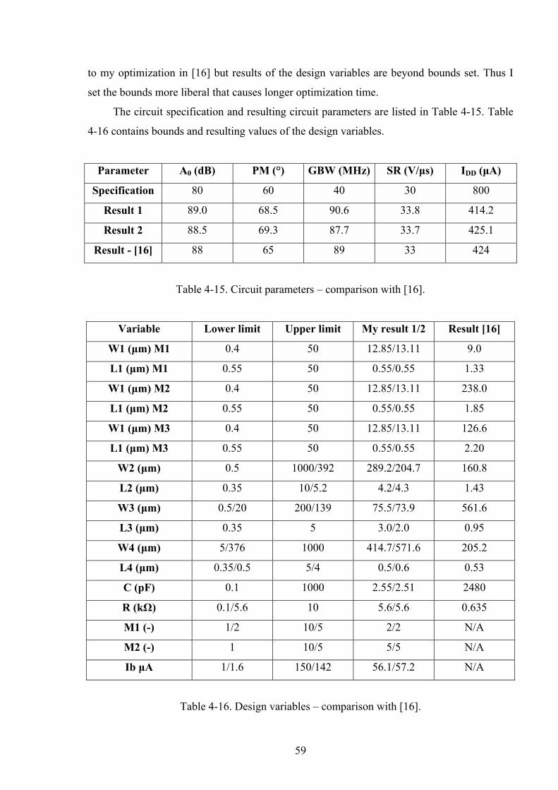
59
to my optimization in [16] but results of the design variables are beyond bounds set. Thus I
set the bounds more liberal that causes longer optimization time.
The circuit specification and resulting circuit parameters are listed in Table 4-15. Table
4-16 contains bounds and resulting values of the design variables.
Parameter A0 (dB) PM (°) GBW (MHz) SR (V/μs) IDD (μA)
Specification 80 60 40 30 800
Result 1 89.0 68.5 90.6 33.8 414.2
Result 2 88.5 69.3 87.7 33.7 425.1
Result - [16] 88 65 89 33 424
Table 4-15. Circuit parameters – comparison with [16].
Variable Lower limit Upper limit My result 1/2 Result [16]
W1 (μm) M1 0.4 50 12.85/13.11 9.0
L1 (μm) M1 0.55 50 0.55/0.55 1.33
W1 (μm) M2 0.4 50 12.85/13.11 238.0
L1 (μm) M2 0.55 50 0.55/0.55 1.85
W1 (μm) M3 0.4 50 12.85/13.11 126.6
L1 (μm) M3 0.55 50 0.55/0.55 2.20
W2 (μm) 0.5 1000/392 289.2/204.7 160.8
L2 (μm) 0.35 10/5.2 4.2/4.3 1.43
W3 (μm) 0.5/20 200/139 75.5/73.9 561.6
L3 (μm) 0.35 5 3.0/2.0 0.95
W4 (μm) 5/376 1000 414.7/571.6 205.2
L4 (μm) 0.35/0.5 5/4 0.5/0.6 0.53
C (pF) 0.1 1000 2.55/2.51 2480
R (kΩ) 0.1/5.6 10 5.6/5.6 0.635
M1 (-) 1/2 10/5 2/2 N/A
M2 (-) 1 10/5 5/5 N/A
Ib μA 1/1.6 150/142 56.1/57.2 N/A
Table 4-16. Design variables – comparison with [16].

60
The bounds are listed as before/after the reduction of the search space since I used
optimization watchdog feature. Because [16] presents powerful circuit I optimized the circuit
only in typical conditions. I was not able to get the same circuit parameters with PVT
analysis.
Optimization time of [16] was 10 hours. Simulation times achieved by developed OT
and watchdog feature were 124 and 120 minutes. First watchdog optimization ended by 8th
population. Solutions were found in the 116th and the 112th populations of the second
watchdog optimizations. Thus the design time using my OT is about 5 times faster. Results of
my simulations were obtained with WDD=0.1 and WDP=1 for the first short optimization and
WDD=0.03 and WDP=5 for the second optimization with modified design variables bounds in
accordance with the first optimization. Conditions of both optimizations were: supply voltage
equal to 2.5 V and load capacitance to 5 pF.
Tables 4-15 and 4-16 contain two optimization results found by my OT where two runs
of the second watchdog optimization were performed. The solutions are very close to each
other. The explanation can be that the tool converges to the same part of the design space with
same optimum. Both solutions of my tool are different from the one mentioned in [16].
Explanations of this fact are the same as those mentioned in other comparison examples.
Last comparison was done with work [17] that is really recent work. It describes
powerful simulation based optimization approach based on Particle Swarm Optimization
algorithm. The comparison was again not easy since results in that article lack the information
about design variables bounds, value of the bias current of the OTA and optimization time of
the design example. Thus the comparison of the optimization running time was not possible.
The goal of the comparison was to achieve as powerful circuit as in [17] and in reasonable
time. Since no specification was mentioned in [17], results of its optimization are used as a
specification in my case.
The circuit specification and resulting circuit parameters are listed in Table 4-17. Table
4-18 contains bounds and resulting values of the design variables (they are listed as
before/after the reduction of the search space since I used optimization watchdog feature).
Because [17] presents powerful circuit I optimized only in typical case. I was not able to get
the same circuit parameter with PVT analysis.
Simulation times achieved by developed OT and watchdog feature were 186 and 192
minutes. First watchdog optimization ended by 11th population. Solutions were found in 82nd
and 85th populations of the second watchdog optimizations. It is very good result if we take
into account that bounds of the design variables were not available and were set very liberally.

61
Results of my simulations were obtained with WDD=0.1 and WDP=1 for the first short
optimization and WDD=0.03 and WDP=5 for the second optimization with modified design
variables bounds in accordance with the first optimization. Conditions of both optimizations
were: supply voltage equal to 3.3 V and load capacitance to 1 pF.
Parameter A0 (dB) PM (°) GBW (MHz) SR (V/μs) IDD (μA)
Specification 81 60 100 288 1819
Result 1 82 63 123 307 1817
Result 2 82 99 122 299 1814
Result - [17] 81 60 N/A 288 1819
Table 4-17. Circuit parameters – comparison with [17].
Variable Lower bound Upper bound My results 1/2 Result [17]
W1 (μm) M1 0.4 100 62.5/36.1 310.0
L1 (μm) M1 0.55 50 0.55/0.55 4.6
W1 (μm) M2 0.4 100 62.5/36.1 432.0
L1 (μm) M2 0.55 50 0.55/0.55 4.1
W1 (μm) M3 0.4 100 62.5/36.1 309.0
L1 (μm) M3 0.55 50 0.55/0.55 2.0
W2 (μm) 5/10 500 87.1/50.1 199.0
L2 (μm) 0.35/1 20/15 6.7/2.9 0.6
W3 (μm) 5/50 500/400 400.0/400.0 245.0
L3 (μm) 0.35/5 20 8.4/13.9 1.3
W4 (μm) 5/20 500 331.8/343.4 360.0
L4 (μm) 0.35 20/11 0.4/0.4 1.4
C (pF) 0.5/5 50 5.0/5.0 3.2
R (kΩ) 0.5 50/30 18.2/15.1 0.545
M1 (-) 1 10 2/3 N/A
M2 (-) 1/2 10 4/7 N/A
Ib (μA) 5/50 500/300 272.8/157.7 N/A
Table 4-18. Design variables – comparison with [17].

62
Tables 4-17 and 4-18 contain two optimization results found by my OT where two runs
of the second watchdog optimization were performed. Another explanation of the result
difference is my different current mirror sizing algorithm mentioned at the beginning of
Chapter 4.1.

63
5 Chip Design and Measurements
I finalized the verification of my OT by measurement of the fabricated chip containing
optimized circuits. The measurement is needed to cover complete analog circuit design flow
from the circuit specification to the fabricated chip measurement. The goal of the verification
is to prove that my OT sizes the circuits in accordance with the input specification.
Following actions were needed to fulfill this task (details of those actions are listed in
this chapter):
• Chip design. I designed the chip schematic containing optimized circuits, pads, bias
distribution circuit and enable logic (to select only the measured circuit to be able to
measure circuit consumption).
• Chip layout. I created the layout of the chip schematic to be sent to the production.
• Chip fabrication. The device was fabricated by the Europractice using AMIS 0.35 μm
CMOS technology.
• Measurements of the chip circuit parameters. I constructed a measurement boards and
measured several fabricated circuits in several corners.
• Discussion of the measurements. I verified the measurement results and compared
measurement conditions with the simulation ones. I performed simulations with the
same conditions as the measurement ones (if they are different) to be able to compare
the measurement results.
5.1 Chip Design
The chip schematic I designed is shown on Figure 5-1. It contains following building
blocks:
• Pads. They are shown in simplified form (as ports) on the figure. The used design kit
contains library with pre-created pads. I used those pads since their design is not the
scope of my work and since their usage speeds-up the chip design significantly. I used
supply and ground pads for supply voltage and ground connections. They are
highlighted in red. I used analog pads for input and output signals. They are
highlighted in blue.

64
• Optimized circuits. They are highlighted in yellow. I placed two-stage Miller OTA
(described in Chapter 4.1), folded cascade OTA (described in Chapter 4.2 – version
with bias current equal to 3.0 μA) and voltage regulator (described in Chapter 4.3) to
the chip.
• Enable logic circuit. It is used to enable just one optimized circuit to enable current
consumption measurement.
• Bias distribution circuit. It is used to enable biasing of all optimized circuits by one
bias current input.
inn
out_ts
inp
vdd
out_fc
vss
out_vr
cs1ibias
voltage reg.
+
-2-stage OTA
+
-fol. cas. OTA
enable logic
en_ts
en_ota
en_t
sib
_ts
en_f
cib
_fc en
_vr
ib_v
r
biasdistributor
ib_tsib_fcib_vr
cs2
en_fcen_vr
Figure 5-1. Chip schematic.
The optimized circuits were slightly modified to be in a defined state when they are
disabled. This is important to not disturb other signals and to be able to measure current
consumption. Disabled circuits are in the state to consume no DC current (except leakage
current). These changes influence the circuit parameters but the effect is negligible. The
modifications of the circuits are:
• Two-stage Miller OTA. Node bias was connected to vss to disable the current
consumption of the circuit. Node out_n was connected to vdd to make the circuit
output floating to not fight with other circuits.

65
• Folded cascode OTA. Node bias_n was connected to vss and node bias_p was
connected to vdd to disable the current consumption of the circuit. Node out_n was
connected to vdd to make the output of the circuit floating not to fight with other
circuits.
• Voltage regulator. Node bias was connected to vss to disable the current consumption
of the circuit. Node reg was connected to vdd to make the circuit output floating to
disable the consumption of the resistor divider.
Bias current for the measured circuits is distributed by the circuit shown on Figure 5-2.
Currents for OTA are generated by one common current mirror since their values are similar
(7.27 and 3.0 μA). Thus it is easy to size the mirror transistors if the transistors in the branch
generating higher current have two transistors in parallel. Separate current mirror is used to
generate current of 100 nA for voltage regulator. All the transistors are sized to be in correct
operation point (strong inversion and saturation) in all corners. The circuit branches are
enabled in accordance with the selected circuit. Transistors dimensions are given in the W/L
format and in μm.
vdd
ibias
M=15.5/0.35
M=25.5/0.35
M=15.5/0.8
M=15.5/0.35
ib_ts ib_fc
M=11.1/0.35
M=11.1/4.1
ib_vr
M=25.5/0.8
M=15.5/0.8
M=11.1/4.1
en_ota_n en_ts_n en_fc_n en_vr_n
M=11.1/0.35
Figure 5-2. Chip bias current distribution circuit schematic.
The enable logic circuit is shown on Figure 5-3. It is used to disable circuits that are
not measured, to enable only the measured circuit and to disable unused branches of the bias
distribution circuit. Chip select cs1 and cs2 input signals are used for this function. It is

66
designed using standard logic cells included in the design kit. The truth table of the circuit is
shown on Figure 5-3.
cs1 en_ts_n
cs2
invcs1_n
invcs2_n
cs2_ncs1 en_ts
cs1_ncs2
inv
inven_fc_n en_fc
nand
nand
cs1cs2
inven_vr_n en_vr
nand
noren_tsen_fc
en_ota_n
cs1 cs200
0
01
11 1
enable
ts OTAfc OTA
v. reg.
none
Figure 5-3. Chip enables logic circuit schematic and its truth table.
Layout of the chip I designed is shown on Figure 5-4. Its dimensions are 871 μm and
775 μm. It was created to be placed to the corner of the MPW (Multi Purpose Wafer). It
contains more structures (not shown on the figure) to be measured in one common pad ring.
My part of the pad ring shown on Figure 5-4 (highlighted by red poly-line) contains
the pads mentioned above in this chapter and one corner pad. This pad is included in the
design kit library and is used only to connect other pads (their metal and diffusion rings). It is
not used to propagate signals outside the chip.
I placed the circuits to be measured (highlighted by red rectangle) inside the pad ring.
There is a gap between these circuits and the pad ring. The gap serves as a routing channel to
propagate signals from the circuits to the pads. Wide supply and ground metal lines are
layouted in the routing channel.
The detailed layout of the measured circuits is shown on Figure 5-5. Its dimensions are
289 μm and 176 μm. It contains both OTA (two-stage and folded cascade), voltage regulator
and support circuits (bias distributor and enable logic). These circuits are highlighted by red
rectangles.

67
Figure 5-4. Chip layout.
Figure 5-5. Chip layout – measured circuits.

68
The capacitor C1 of the two-stage OTA consumes more than 60 % of the circuit area.
If the area is too big for the application, it can be solved by resetting of the higher bound of
the design variable C. It can be also solved by introduction of the area optimization to the OT.
The question is if the same specification can be reached with lower value of the C1
capacitance.
The resistors R1 and R2 of the voltage regulator consume more than 75 % of the
circuit area. If the area is too big for the application, it can be solved by increasing of the
resistor divider consumption or by using of the resistor with higher sheet resistance.
The chip layout gds file was sent to the Europractice to be fabricated. Its photo is not
shown in my thesis since my circuits are not visible because of metal fillers.
5.2 Measurement Board
The chip was encapsulated to the DIL40 package. Table 5-1 summarizes connections
of my circuit to the package terminals. Names of nodes in my circuit are the same as on
Figure 5-1.
Terminal number Node in the circuit Terminal number Node in the circuit
1 vdd 6 Inp
2 ibias 7 Inn
3 cs1 8 out_ts
4 cs2 9 out_fc
5 vss 40 out_vr
Table 5-1. Connection of my circuit to the chip package.
I took the following considerations into account during the measurements board
design:
• Impossible to measure the zero frequency OTA gain. The stable input AC signal with
amplitude lower than 1 mV is needed to measure the gain higher than 60 dB. It was
not possible to achieve such a signal because of noise and available measurement
instruments. PM and GBW are measured using the typical inverting amplifier

69
connection with 20 dB zero frequency gain. This configuration has the same AC
characteristic around unity gain bandwidth frequency [40] thus it is sufficient for GBW
and PM measurement.
• Impossible to measure bandwidth and phase margin of the voltage regulator feedback
loop. The reason is that the feedback loop is inside the voltage regulator (inside the
chip).
• Impossible to measure PSRR of the voltage regulator at the 50 Hz frequency. The
reason is the noise caused by the 50 Hz supply of the measurement instruments. The
noise caused by other equipment in the laboratory with 50 Hz supply disturbed the
measurement as well.
• It must be possible to insert the chip to the temperature chamber for temperature
measurements. The only available chamber is so small, that the complete measurement
board is not fitting to it.
• The bias current and voltage regulator current load are generated by resistors
connected to ground. Bias current corner measurements are not swept. It was decided
not to measure them to decrease significant number of the measurement corners. If the
specification meets the measurement, it is clear from other measurement anyway.
The layout of the measurement board is shown on Figure 5-6. The photo of the
constructed board is shown on the figure as well. The yellow highlighting of the measurement
board layout determines the board shape. The red highlighting shows the position of the chip
package. The dashed lines represent the connection made via wires. The black dots show the
connections of those wires to the board. The terminals are used to connect supply sources and
measurement equipment. The jumpers are used to choose:
• The circuit to be measures by cs1 and cs2 signals.
• Resistors for the OTAs connections to form inverting amplifier with 20 dB gain.
• OTA output to be connected to the board.
• Load of the voltage regulator.
• Resistor to create bias current for the measured circuits.
The x and y dimensions of the board are 10 cm and 16 cm respectively. The chip is
inserted to the narrow part of the board that can be inserted to the temperature chamber.

70
Figure 5-6. Measurement board.
5.3 Circuit Measurements
I measured all circuit on three samples except the current consumption measured on
one sample. The current consumption was disturbed by other circuits present on the MPW
even when the circuits were disabled by the board modification. Thus it was difficult to
achieve stable not disturbed current consumption. One chip measurement was done for the
information purposes not for real verification.
It was found that the worst cases of some circuit parameters were determined
incorrectly during the measurement and optimization comparison. The reason is that the worst
cases were determined in accordance with three circuit versions only. An improvement of the
OT will be made. The circuit parameters worst cases will be based on several tenths of
random circuit simulations. The optimized circuit parameter values and real worst case
simulation results (based on all corner simulations) of those circuits are listed below for each
71
design examples. Also the change in the worst case corner is listed there. The corner is
different in some cases but the parameter value is the same. It means that the specific PVT
corner does not impact that parameter much.
I discovered that the resistor used in the chip circuits (two-stage OTA and voltage
regulator) has different resistance on the chip than in the optimized circuits. The resistors had
width 1.5 μm and number of squares was the design variable. The width was changed to 0.8
μm to decrease the area of the circuits. But I changed the number of squares thinking I need to
change the length of the resistors. This leads to different AC characteristics of the two-stage
OTA. It causes also higher consumption of the voltage regulator resistor divider.
5.3.1 Two-Stage Miller OTA Measurements
The optimized circuit parameter values, real worst case values and change in the worst
case corners are listed in Table 5-2. The circuit parameters I measured are highlighted in bold
type.
Parameter Optimized value Worst case value Corner change
A0 (dB) 89.6 89.6 no change – corner correct
PM (°) 62.8 60.9 Temp max, VDD min, IB min
GBW (MHz) 1.65 1.458 RES min
SR (V/μs) 1.05 0.94 RES min
IDD (μA) 48.8 50.1 CAP min, VDD min
Table 5-2. The worst case corner changes of the two-stage Miller OTA.
The probes are needed for the AC characteristic measurements (to be able to measure
using phase meter and oscilloscope). Only available probes create load of 96 pF and 10 MΩ.
This load is different from the one used in optimization (10 pF only). Thus the simulation of
the circuit with the probe load is needed to compare measurement with simulation. Moreover
the measurement using phase meter creates capacitance between inputs of the phase meter.
This capacitance must be also taken into account in these comparison simulations. GBW and
PM of the OTA are measured in the inverting amplifier configuration. The load of the
resistive feedback is also taken into account in the comparison simulations. The 10 kΩ and the
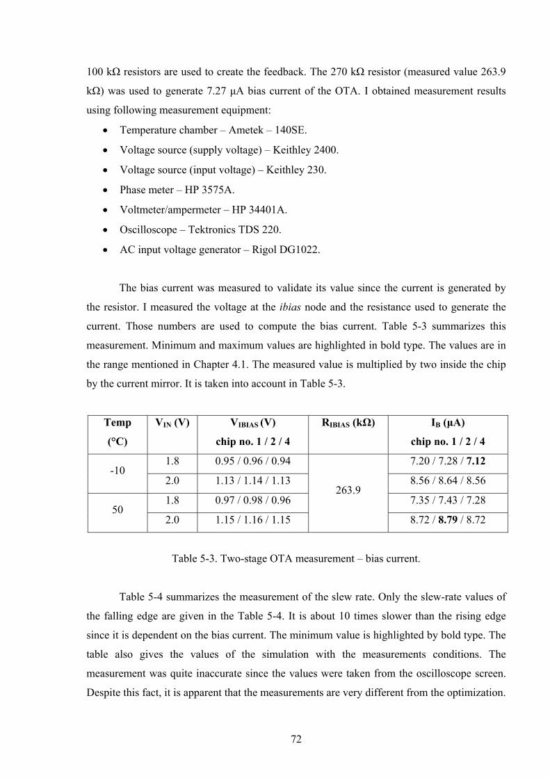
72
100 kΩ resistors are used to create the feedback. The 270 kΩ resistor (measured value 263.9
kΩ) was used to generate 7.27 μA bias current of the OTA. I obtained measurement results
using following measurement equipment:
• Temperature chamber – Ametek – 140SE.
• Voltage source (supply voltage) – Keithley 2400.
• Voltage source (input voltage) – Keithley 230.
• Phase meter – HP 3575A.
• Voltmeter/ampermeter – HP 34401A.
• Oscilloscope – Tektronics TDS 220.
• AC input voltage generator – Rigol DG1022.
The bias current was measured to validate its value since the current is generated by
the resistor. I measured the voltage at the ibias node and the resistance used to generate the
current. Those numbers are used to compute the bias current. Table 5-3 summarizes this
measurement. Minimum and maximum values are highlighted in bold type. The values are in
the range mentioned in Chapter 4.1. The measured value is multiplied by two inside the chip
by the current mirror. It is taken into account in Table 5-3.
Temp
(°C)
VIN (V) VIBIAS (V)
chip no. 1 / 2 / 4
RIBIAS (kΩ) IB (μA)
chip no. 1 / 2 / 4
1.8 0.95 / 0.96 / 0.94 7.20 / 7.28 / 7.12 -10
2.0 1.13 / 1.14 / 1.13 8.56 / 8.64 / 8.56
1.8 0.97 / 0.98 / 0.96 7.35 / 7.43 / 7.28 50
2.0 1.15 / 1.16 / 1.15
263.9
8.72 / 8.79 / 8.72
Table 5-3. Two-stage OTA measurement – bias current.
Table 5-4 summarizes the measurement of the slew rate. Only the slew-rate values of
the falling edge are given in the Table 5-4. It is about 10 times slower than the rising edge
since it is dependent on the bias current. The minimum value is highlighted by bold type. The
table also gives the values of the simulation with the measurements conditions. The
measurement was quite inaccurate since the values were taken from the oscilloscope screen.
Despite this fact, it is apparent that the measurements are very different from the optimization.

73
The possible explanation is higher load of the probe than the specified number. Since it
explains also differences of the GBW and PM measurements and also the differences of the
folded cascade parameter measurements, the higher load of the probe is more probable. The
simulation values shown in Table 5-4 were performed for 300 pF probe capacitive load,
measured bias current values, typical silicon corners and temperature and bias corners the
same as the measured ones. Measured values are much closer to the simulated ones than to the
optimized value (0.94 V/μs).
Temp (°C) VIN (V) SRMEAS (V/μs) chip no. 1 / 2 / 4 SRSIM (V/μs)
1.8 0.19 / 0.19 / 0.19 0.050 -10
2.0 0.22 / 0.22 / 0.24 0.060
1.8 0.18 / 0.19 / 0.19 0.051 50
2.0 0.22 / 0.22 / 0.24 0.057
Table 5-4. Two-stage OTA measurement – slew-rate.
Table 5-5 gives results of the current consumption measurement results. The OTA
current consumption IDD is given as:
BYSDDBMEASDDDD IIII −−∗−= __ )5.1( (5-1)
where IDD_MEAS is the measured value, IB is the OTA bias current and IDD_S-BY is the
stand-by current of the chip including other structures than my circuit. The IDD_S-BY current
was very unstable thus it was hard to measure this parameter. Maximum measured IDD is
highlighted by bold type in Table 5-5. This value is lower than the optimized one.
Temp (°C) VIN (V) IB (μA) IDD_MEAS (μA) IDD_S-BY (μA) IDD (μA)
1.8 7.20 41.2 0.0 30.4 -10
2.0 8.56 49.5 0.0 36.7
1.8 7.35 105.0 62.8 31.2 50
2.0 8.72 116.3 65.8 37.5
Table 5-5. Two-stage OTA measurement – current consumption.

74
-10
-5
0
5
10
15
20
25
1 10 100 1000
Frequency (kHz)
Gai
n (d
B)
chip 1 -10/1,8 chip 1 -10/2,0 chip 1 50/1,8 chip 1 50/2,0chip 2 -10/1,8 chip 2 -10/2,0 chip 2 50/1,8 chip 2 50/2,0chip 4 -10/1,8 chip 4 -10/2,0 chip 4 50/1,8 chip 4 50/2,0
Figure 5-7. Measurement results of two-stage Miller OTA gain.
-10
10
30
50
70
90
110
130
150
170
190
1 10 100 1000
Frequency (kHz)
Phas
e (°
)
chip 1 -10/1,8 chip 1 -10/2,0 chip 1 50/1,8 chip 1 50/2,0chip 2 -10/1,8 chip 2 -10/2,0 chip 2 50/1,8 chip 2 50/2,0chip 4 -10/1,8 chip 4 -10/2,0 chip 4 50/1,8 chip 4 50/2,0
Figure 5-8. Measurement results of two-stage Mille OTA phase.

75
Measured gain and phase characteristics of the inverting amplifier using measured
two-stage Miller OTA are shown ion Figure 5-7 and Figure 5-8 for all measured chips and all
measured corners.
Measured values of PM and GBW are in Table 5-6 together with simulated values in
the specific corners using the measured bias current. These simulations were done for
different conditions than the optimization since the conditions are different.
Temp (°C) VIN (V) PMMEAS (°) chip
no. 1 / 2 / 4
PMSIM (°) GBWMEAS (kHz)
chip no. 1 / 2 / 4
GBWSIM
(kHz)
1.8 10.0 / 8.9 / 8.7 6.4 820 / 820 / 850 720 -10
2.0 10.1 / 9.9 / 8.8 6.1 910 / 930 / 940 837
1.8 9.3 / 9.7 / 9.1 6.8 770 / 800 / 810 658 50
2.0 10.9 / 9.6 / 9.1 6.5 860 / 880 / 890 758
Table 5-6. Two-stage OTA measurement – GBW and PM.
The differences between optimization and measurement conditions are inductance of
the bonding wires, pads of the IC, different OTA resistor value as mentioned in Chapter 5.3
and additional disabling circuitry of the OTA. The main factors affecting different
optimization and measurement results are:
• Different load of the OTA caused by the measurement probe. The specified load of the
probe is 96 pF and 1 MΩ but it seems that the actual capacitive load is about 300 pF.
• Feedback loop to create inverting amplifier with 20 dB gain from the OTA. It was
used to be able to measure the frequency characteristics.
• Additional unknown capacitance between phase meter probes. One probe was
connected to the output of the OTA and the second was to the input signal source.
This capacitance was estimated to 200 pF.
Table 5-7 gives details of the optimized (the worst case simulation results mentioned
in Table 5-2) and measured circuit parameters values. Additionally, results of the comparison
simulations are given there (if applicable) to be compared with measured ones.
A0 was not measured and IDD measured value is better then the optimized one. Other
measurements are far from the optimized ones mainly due to different load of the circuit.
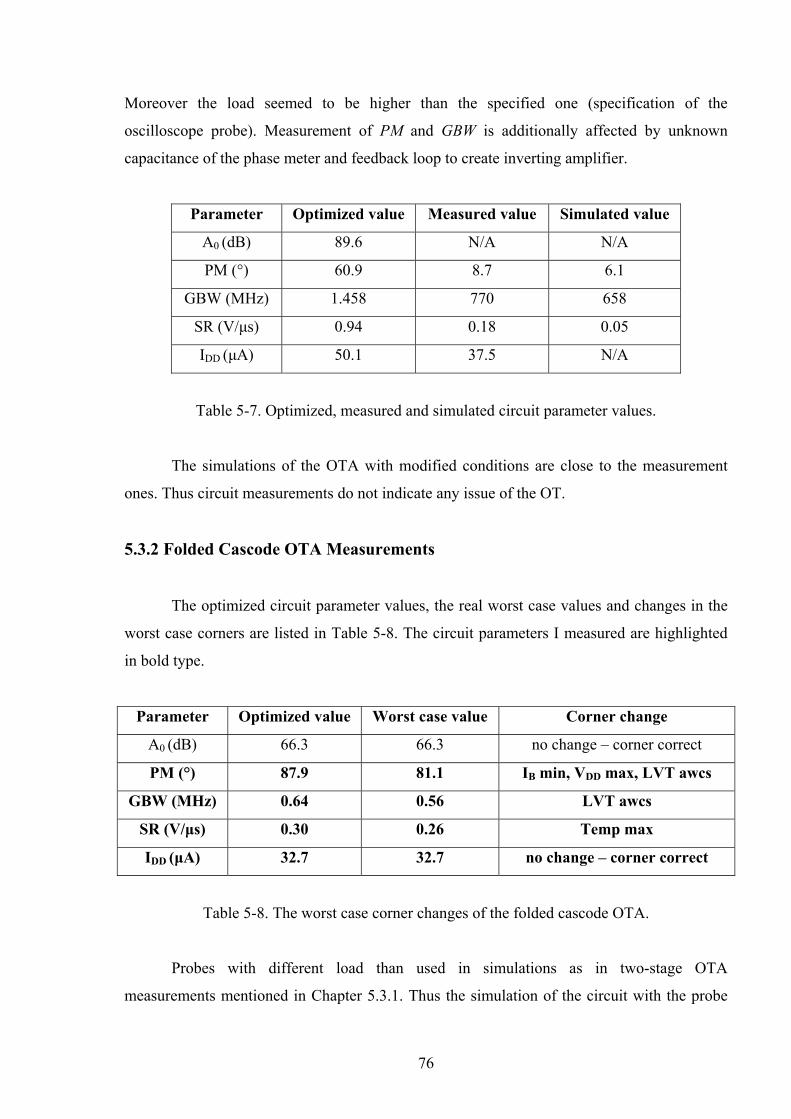
76
Moreover the load seemed to be higher than the specified one (specification of the
oscilloscope probe). Measurement of PM and GBW is additionally affected by unknown
capacitance of the phase meter and feedback loop to create inverting amplifier.
Parameter Optimized value Measured value Simulated value
A0 (dB) 89.6 N/A N/A
PM (°) 60.9 8.7 6.1
GBW (MHz) 1.458 770 658
SR (V/μs) 0.94 0.18 0.05
IDD (μA) 50.1 37.5 N/A
Table 5-7. Optimized, measured and simulated circuit parameter values.
The simulations of the OTA with modified conditions are close to the measurement
ones. Thus circuit measurements do not indicate any issue of the OT.
5.3.2 Folded Cascode OTA Measurements
The optimized circuit parameter values, the real worst case values and changes in the
worst case corners are listed in Table 5-8. The circuit parameters I measured are highlighted
in bold type.
Parameter Optimized value Worst case value Corner change
A0 (dB) 66.3 66.3 no change – corner correct
PM (°) 87.9 81.1 IB min, VDD max, LVT awcs
GBW (MHz) 0.64 0.56 LVT awcs
SR (V/μs) 0.30 0.26 Temp max
IDD (μA) 32.7 32.7 no change – corner correct
Table 5-8. The worst case corner changes of the folded cascode OTA.
Probes with different load than used in simulations as in two-stage OTA
measurements mentioned in Chapter 5.3.1. Thus the simulation of the circuit with the probe

77
load is needed to compare measurement with simulation. Capacitance created by the phase
meter and load of the resistive feedback (1 MΩ and 10 MΩ) are takes into account in this
simulation as well. The 270 kΩ resistor (measured value 263.9 kΩ) was used to generate 3.0
μA bias current of the OTA. I obtained measurement results using same measurement
equipment as in the measurement case mentioned in Chapter 5.3.1.
The bias current was measured to validate its value since the current is generated by
the resistor. I measured the voltage at the ibias node and the resistance used to generate the
current. Those numbers are used to compute the bias current. Table 5-9 summarizes this
measurement. Minimum and maximum values are highlighted in bold type. The values are in
the range mentioned in Chapter 4.2.
Temp
(°C)
VIN (V) VIBIAS (V)
chip no. 1 / 2 / 4
RIBIAS (kΩ) IBI (μA)
chip no. 1 / 2 / 4
1.8 0.95 / 0.96 / 0.95 3.60 / 3.64 / 3.60 -10
2.0 1.13 / 1.14 / 1.13 4.28 / 4.32 / 4.28
1.8 0.97 / 0.98 / 0.96 3.68 / 3.71 / 3.64 50
2.0 1.15 / 1.16 / 1.14
263.9
4.36 / 4.40 / 4.32
Table 5-9. Folded cascode OTA measurement – bias current.
Table 5-10 summarizes the measurement of the slew rate. Only the worst case values
are given in the Table 5-10. Falling edge is the worst case. The same result was obtained by
the simulations. The minimum value is highlighted by bold type.
Temp (°C) VIN (V) SRMEAS (V/μs) chip no. 1 / 2 / 4 SRSIM (V/μs)
1.8 0.036 / 0.039 / 0.035 0.023 -10
2.0 0.057 / 0.059 / 0.055 0.033
1.8 0.039 / 0.040 / 0.036 0.024 50
2.0 0.057 / 0.059 / 0.055 0.034
Table 5-10. Folded cascode OTA measurement – slew-rate.

78
The table gives the values of the simulation with the measurements conditions. The
measurement was quite inaccurate since the values were taken from the oscilloscope screen as
in the two-stage OTA case mentioned in Chapter 5.3.1.
The simulation values shown in Table 5-9. were performed for 300 pF capacitive load
as in the case mentioned in Chapter 5.3.1. Other simulation conditions are: measured bias
current values, typical silicon, temperature and bias corners equal to the measured ones.
Measured values are very close to the simulated ones for the modified capacitive load.
Table 5-11 gives results of the current consumption measurement results. Maximum
measured IDD is highlighted by bold type.
Temp (°C) VIN (V) IB (μA) IDD_MEAS (μA) IDD_S-BY (μA) IDD (μA)
1.8 3.60 62.9 25.1 30.6 -10
2.0 4.28 63.4 18.1 36.8
1.8 3.68 102.8 64.7 30.8 50
2.0 4.36 114.6 68.8 37.1
Table 5-11. Folded cascode OTA measurement – current consumption.
The OTA current consumption IDD is given as:
BYSDDBMEASDDDD IIII −−∗−= __ )2( (5-2)
where IDD_MEAS is the measured value, IB is the OTA bias current and IDD_S-BY is the
stand-by current of the complete chip. It is about 4.4 μA higher than the maximum simulated
one. It can be explained by very unstable IDD_S-BY.
Measured gain and phase characteristics of the inverting amplifier using measured
folded cascode OTA are shown on Figure 5-9 and Figure 5-10 for all measured chips and all
measured corners. The measured values of PM and GBW are in Table 5-12.
It is apparent that the feedback resistors overloaded the OTA thus the A0 is only about
17.5 dB. Table 5-12 contains simulated values in the specific corners using the measured bias
current (the worst cases are highlighted by bold type). These simulations were done for
different conditions than the optimization since the conditions are different. The conditions
were the same as mentioned in Chapter 5.3.1.

79
-5
0
5
10
15
20
0.01 0.10 1.00 10.00 100.00
Frequency (kHz)
Gai
n (d
B)
chip 1 -10/1,8 chip 1 -10/2,0 chip 1 50/1,8 chip 1 50/2,0chip 2 -10/1,8 chip 2 -10/2,0 chip 2 50/1,8 chip 2 50/2,0chip 4 -10/1,8 chip 4 -10/2,0 chip 4 50/2,0 chip 4 50/2,0
Figure 5-9. Measurement results of folded cascade OTA gain.
40
60
80
100
120
140
160
180
0.01 0.10 1.00 10.00 100.00Frequency (kHz)
Pha
se (
°)
chip 1 -10/1,8 chip 1 -10/2,0 chip 1 50/1,8 chip 1 50/2,0chip 2 -10/1,8 chip 2 -10/2,0 chip 2 50/1,8 chip 2 50/2,0chip 4 -10/1,8 chip 4 -10/2,0 chip 4 50/1,8 chip 4 50/2,0
Figure 5-10. Measurement results of folded cascade OTA phase.

80
Temp (°C) VIN (V) PMMEAS (°) chip
no. 1 / 2 / 4
PMSIM (°) GBWMEAS (kHz)
chip no. 1 / 2 / 4
GBWSIM
(kHz)
1.8 67.0 / 67.3 / 66.8 72.3 14.3 / 14.5 / 14.2 10.3 -10
2.0 68.0 / 68.1 / 67.8 72.4 16.2 / 16.3 / 16.1 13.9
1.8 67.2 / 67.5 / 67.6 73.5 14.0 / 14.1 / 13.8 9.9 50
2.0 68.6 / 68.8 / 68.4 72.6 15.6 / 15.6 / 15.5 12.9
Table 5-12. Folded cascode OTA measurement – GBW and PM.
Table 5-13 gives details of the optimized (the worst case simulation results mentioned
in Table 5-8) and measured circuit parameters values. Additionally, results of the comparison
simulations are given there (if applicable) to be compared with measured ones.
A0 was not measured. IDD measured is slightly higher than the optimized one. It can be
explained by the consumption of the other blocks on the chip. Other measurements are far
from the optimized ones due to the same effects as in the two-stage OTA case mentioned in
Chapter 5.3.1. They are different load of the circuit, unknown capacitance of the phase meter
and feedback loop to create inverting amplifier.
Parameter Optimized value Measured value Simulated value
A0 (dB) 66.3 N/A N/A
PM (°) 81.1 67.0 72.3
GBW (kHz) 560 13.8 9.9
SR (V/μs) 0.26 0.035 0.023
IDD (μA) 32.7 37.1 N/A
Table 5-13. Optimized, measured and simulated circuit parameter values.
The simulations of the OTA with modified conditions are close to the measurement
ones. Thus circuit measurements do not indicate any issue of the OT.
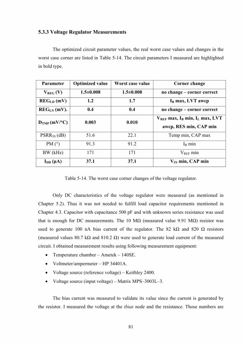
81
5.3.3 Voltage Regulator Measurements
The optimized circuit parameter values, the real worst case values and changes in the
worst case corner are listed in Table 5-14. The circuit parameters I measured are highlighted
in bold type.
Parameter Optimized value Worst case value Corner change
VREG (V) 1.5±0.008 1.5±0.008 no change – corner correct
REGLD (mV) 1.2 1.7 IB max, LVT awcp
REGLN (mV). 0.4 0.4 no change – corner correct
DTMP (mV/°C) 0.003 0.010 VREF max, IB min, IL max, LVT
awcp, RES min, CAP min
PSRR50 (dB) 51.6 22.1 Temp min, CAP max
PM (°) 91.3 91.2 IB min
BW (kHz) 171 171 VREF min
IDD (μA) 37.1 37.1 VIN min, CAP min
Table 5-14. The worst case corner changes of the voltage regulator.
Only DC characteristics of the voltage regulator were measured (as mentioned in
Chapter 5.2). Thus it was not needed to fulfill load capacitor requirements mentioned in
Chapter 4.3. Capacitor with capacitance 500 pF and with unknown series resistance was used
that is enough for DC measurements. The 10 MΩ (measured value 9.91 MΩ) resistor was
used to generate 100 nA bias current of the regulator. The 82 kΩ and 820 Ω resistors
(measured values 80.7 kΩ and 810.2 Ω) were used to generate load current of the measured
circuit. I obtained measurement results using following measurement equipment:
• Temperature chamber – Ametek – 140SE.
• Voltmeter/ampermeter – HP 34401A.
• Voltage source (reference voltage) – Keithley 2400.
• Voltage source (input voltage) – Matrix MPS–3003L–3.
The bias current was measured to validate its value since the current is generated by
the resistor. I measured the voltage at the ibias node and the resistance. Those numbers are

82
used to compute the bias current. Table 5-15 summarizes this measurement. Minimum and
maximum values are highlighted in bold type. The values are in the range mentioned in
Chapter 4.3. The bias current is measured only for temperature and input voltage corners
since only those corners influence the current value.
Temp
(°C)
VIN (V) VIBIAS (V)
chip no. 1 / 2 / 4
RIBIAS (MΩ) IBI (nA)
chip no. 1 / 2 / 4
1.8 0.95 / 0.97 / 0.93 96.9 / 97.9 / 93.8 -10
2.0 1.12 / 1.12 / 1.10 113 / 113 / 111
1.8 0.96 / 0.98 / 0.94 96.9 / 98.9 / 94.9 50
2.0 1.14 / 1.14 / 1.12
9.91
115 / 115 / 113
Table 5-15. Voltage regulator measurement – bias current.
Temp (°C) VIN (V) VREF (V) IL (μA) VREG (V) – chip no. 1 / 2 / 4
18.5 1.4907 / 1.4901 / 1.4911 1.23
1830 1.4816 / 1.4812 / 1.4829
18.6 1.5027 / 1.5021 / 1.5031 1.8
1.24
1840 1.4936 / 1.4931 / 1.4947
18.5 1.4908 / 1.4901 / 1.4911 1.23
1830 1.4820 / 1.4813 / 1.4831
18.6 1.5027 / 1.5021 / 1.5031
-10
2.0 1.24
1840 1.4939 / 1.4933 / 1.4950
18.5 1.4905 / 1.4901 / 1.4918 1.23
1830 1.4804 / 1.4788 / 1.4820
18.6 1.5025 / 1.5020 / 1.5038 1.8
1.24
1840 1.4923 / 1.4903 / 1.4938
18.5 1.4905 / 1.4901 / 1.4919 1.23
1830 1.4808 / 1.4800 / 1.4822
18.6 1.5025 / 1.5021 / 1.5039
50
2.0 1.24
1840 1.4927 / 1.4919 / 1.4945
Table 5-16. Voltage regulator measurement – regulated voltage.

83
Table 5-16 summarizes the measurement of the regulated voltage. The minimum and
maximum values are highlighted by bold type (for each measured chip). The table also
summarizes load current of the voltage regulator generated by resistors.
The measured value of VREG is 1.491±0.013 V. The difference between simulation and
measurement is 8 mV of the nominal values and 4 mV of the voltage spread. The difference is
very small and can be explained partly by uncertainty of the measurement equipment and
noise present during the measurements. It would be better to compare simulations and
measurements for the circuit with higher values of the circuit parameter – spread of the VREG
in this case. Other explanations can be:
• Resistor mismatch. Layout of the resistors R1 and R2 is not ideal and could be
improved to minimize the nominal VREG value mainly. A change of their ratio by 1%
causes 2.7 mV nominal VREG values change. This effect was not taken into account in
the optimization.
• Reference voltage instability. A change of VREF by 1 mV would cause 1.2 mV VREG
change.
• Differential pair offset. The offset of the differential pair in the feedback loop can
cause similar VREG change as the reference voltage instability.
• Resistance of the output pad. Simulations of the pad shows that the voltage drop on
the pad is 0.015 mV thus this effect is negligible.
• Resistance of the chip package bonding and metal routing inside chip. This
phenomenon has the same effect as the pad resistance but can not be simulated. Every
1 Ω of this resistance creates drop of 2 mV with 2 mA ILOAD current.
Measured values of VREG were used to compute REGLD, REGLN and DTMP. Maximum
measured values of those circuit parameters are:
• REGLN – 1.6 mV (conditions: Temp = 50 °C, VREF = 1.24 V, IL = 1840 μA)
• REGLD – 11.7 mV (conditions: Temp = 50 °C, VREF = 1.24 V, VIN = 1.8 V)
• DTMP – 0.047 mV/°C (conditions: VREF = 1.24 V, VIN = 1.8 V, IL = 1840 μA)
Those values are about 5 times higher than those I simulated. On the other hand they
are hard to measure precisely due to low values close to measurement equipment possibilities.
Higher value of REGLD can be explained by resistive paths of few Ω between the voltmeter
and the voltage regulator (caused by chip bonding and chip routing metals).
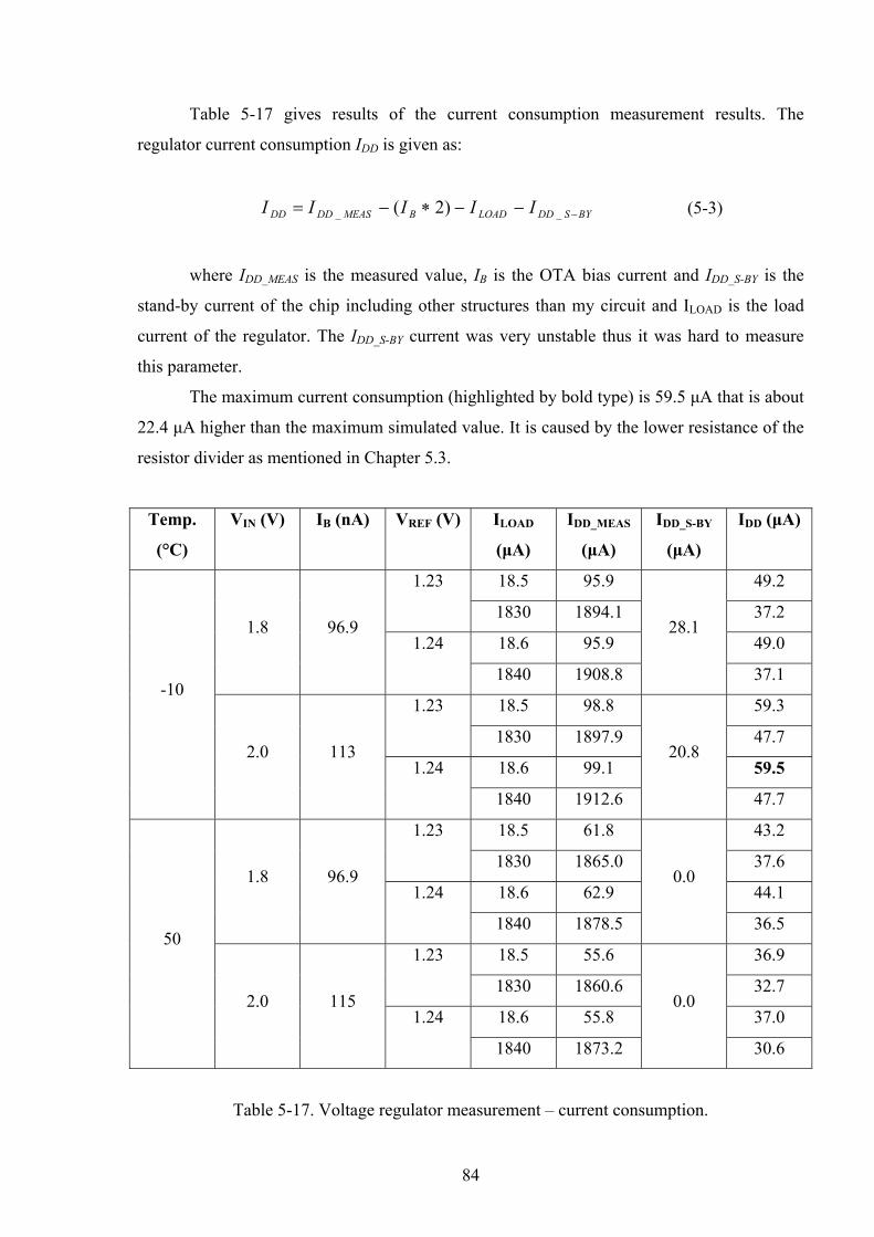
84
Table 5-17 gives results of the current consumption measurement results. The
regulator current consumption IDD is given as:
BYSDDLOADBMEASDDDD IIIII −−−∗−= __ )2( (5-3)
where IDD_MEAS is the measured value, IB is the OTA bias current and IDD_S-BY is the
stand-by current of the chip including other structures than my circuit and ILOAD is the load
current of the regulator. The IDD_S-BY current was very unstable thus it was hard to measure
this parameter.
The maximum current consumption (highlighted by bold type) is 59.5 μA that is about
22.4 μA higher than the maximum simulated value. It is caused by the lower resistance of the
resistor divider as mentioned in Chapter 5.3.
Temp.
(°C)
VIN (V) IB (nA) VREF (V) ILOAD
(μA)
IDD_MEAS
(μA)
IDD_S-BY
(μA)
IDD (μA)
18.5 95.9 49.2 1.23
1830 1894.1 37.2
18.6 95.9 49.0 1.8 96.9
1.24
1840 1908.8
28.1
37.1
18.5 98.8 59.3 1.23
1830 1897.9 47.7
18.6 99.1 59.5
-10
2.0 113 1.24
1840 1912.6
20.8
47.7
18.5 61.8 43.2 1.23
1830 1865.0 37.6
18.6 62.9 44.1 1.8 96.9
1.24
1840 1878.5
0.0
36.5
18.5 55.6 36.9 1.23
1830 1860.6 32.7
18.6 55.8 37.0
50
2.0 115 1.24
1840 1873.2
0.0
30.6
Table 5-17. Voltage regulator measurement – current consumption.

85
Table 5-18 gives details of the optimized (the worst case simulation results mentioned
in Table 5-14) and measured circuit parameters values.
Parameter Optimized value Measured value
VREG (V) 1.500±0.008 1.491±0.013
REGLD (mV) 1.7 11.7
REGLN (mV). 0.4 1.6
DTMP (mV/°C) 0.010 0.047
PSRR50 (dB) 22.1 N/A
PM (°) 91.2 N/A
BW (kHz) 171 N/A
IDD (μA) 37.1 59.5
Table 5-18. Optimized, measured and simulated circuit parameter values.
PSRR50, PM and BW were not measured. IDD measured value is higher then the
optimized one. It can be explained by lower resistance of the resistor divider.
VREG measurements are slightly beyond the optimized range. Main explanations are
resistor divider mismatch, reference voltage instability and differential pair mismatch. The
target values are also easily disturbed by the noise (are in range of mV).
Other measured parameters - REGLD, REGLN and DTMP – are beyond the optimized
values. Since these parameters are derived from VREG measurements, they are affected by
same disturbing phenomenon. Since their values are quite low the measurements are affected
by uncertainty of the measurement equipment. High measured value of REGLD can be
explained by additional output resistance created by routing inside chip and chip.
The measured values are close to the measurement ones. Thus circuit measurements
do not show any issue of the OT.

86
6 General Conclusions
I have created a novel OT for automated industry design of analog IC. The tool is
implemented in the Cadence design environment, and a very short setup time is achieved. The
integration with Cadence also makes the use of the OT convenient and any improvements and
extensions possible. The tool uses the most accurate simulation based optimization approach
and a robust version of differential evolution algorithm, thus it is able to optimize a generic
circuit architecture. The OT optimizes circuits using a full PVT analysis, ensuring robust
resulting circuits that are usually ready to use.
An Optimization watchdog feature was developed to enhance the circuit optimization.
This novel feature was implemented to the OT. Its main purpose is to reduce the search space
and thus to accelerate the optimization progress leading to a shorter automated design time.
This acceleration even allows the OT to find better circuits, which would not be found
otherwise. The reason is that their optimization would take so long time that the optimization
would be stopped before they are found. The optimization watchdog can speed up the
optimization by a factor more than two as described in Chapter 4.5.
Another novel feature for accurate current mirror automated design was introduced,
and implemented to the OT. It is based on extracting the dimensions of transistors in
accordance with the current flowing through the transistors. Their matching is more accurate
in comparison with the random transistor sizing presented in [16][17][24][25][26]. This novel
approach was used successfully in the optimization of three design examples described in
Chapters 4.1, 4.2 and 4.3.
Most important scientific contributions of this work are:
• Novel optimization watchdog feature
o reduces the design space during the optimization progress to improve the
convergence and the quality of results.
o controls the optimization progress to reduce the optimization time.
• Novel algorithm for design of accurate current mirrors
o computes the size of the transistors in accordance with the current flowing
through them, as opposed to random sizing used elsewhere..
o all transistors in the mirror have the same dimensions. Different currents in
different branches are achieved by placing several transistors in parallel.

87
• The first OT ever able to optimize analog circuits by full PVT simulation. The PVT
simulations usually ensure accurate ready-to-use resulting circuits.
• OT with a very short setup time.
o No need to create circuit schematic, test-benches and to define extraction of the
circuit parameters. Design examples are re-usable.
o OT is implemented in a widely used design environment.
I compared my OT with the works presented recently [13][16][17], on the basis of a
two-stage Miller OTA design example, which is the most frequently used circuit in automated
design approaches. The comparison was slightly difficult since not all details needed to
compare the results fully were presented, as mentioned in Chapter 4.6.
Load capacitance of the sized circuit is not mentioned in [13]. I chose load capacitance
of 1 pF. The value of the bias current of the circuit is not presented in [16]. Design variables
bounds are not defined in [17]. Also the bias current value is not mentioned there. This works
lacks the information about the optimization time of the design example, which cannot be
compared therefore. So, the goal was to achieve as powerful circuit as in [17] in a reasonable
time.
Another point of difference is that optimizations done by the proposed OT use the novel
current mirror sizing approach. Thus my results are more accurate generally. The
specifications, the resulting circuit parameters and the optimization times are given in Tables
6-1, 6-2 and 6-3.
Parameter A0 (dB) PM (°) GBW (MHz) SR (V/μs) IDD (μA) Time (min)
Specification 70 60 1.0 1.0 75 N/A
Result 1 86 68 2.5 1.0 42 51
Result 2 86 66 3.3 1.7 28 63
Result - [13] 92 63 1.7 1.0 70 32
Table 6-1. Circuit parameters – comparison with [13].
The differences between [13] and my optimization are that CMRR is optimized to 90
dB and typical simulations only are used in [13]. I do not optimize CMRR and I use PVT

88
simulation to obtain the result. The optimization time of [13] is shorter, on the other hand, I
used PVT simulations, resulting in a robust circuit.
Parameter A0 (dB) PM (°) GBW (MHz) SR (V/μs) IDD (μA) Time (min)
Specification 80 60 40 30 800 N/A
Result 1 89.0 68.5 90.6 33.8 414.2 124
Result 2 88.5 69.3 87.7 33.7 425.1 120
Result - [16] 88 65 89 33 424 600
Table 6-2. Circuit parameters – comparison with [16].
3dB frequency and noise are optimized in [16] in addition to optimization using
proposed OT, on the other hand, results of the design variables are beyond their bounds. Thus
I set the bounds more liberally, causing a longer optimization time. I optimized the circuit
only in typical conditions and used optimization watchdog feature, so that a much shorter
optimization time was achieved.
Parameter A0 (dB) PM (°) GBW (MHz) SR (V/μs) IDD (μA) Time (min)
Specification 81 60 100 288 1819 N/A
Result 1 82 63 123 307 1817 186
Result 2 82 99 122 299 1814 192
Result - [17] 81 60 N/A 288 1819 N/A
Table 6-3. Circuit parameters – comparison with [17].
The comparison with [17] was run using typical simulations only. The Optimization
watchdog feature was used to reduce optimization time. The OT comparison is not
unambiguous since the optimization conditions of the approaches differ considerably. Still my
OT seems to be at least comparable with other works presented so far. Thus it seems that my
OT is competitive to other tools for analog circuit automated design. Moreover, my OT
involves three novel features, improving the optimization leading to better result. These
features are:
• The Optimization watchdog.

89
• The novel current mirror sizing algorithm.
• An option to use the PVT analysis.
The simple but robust differential evolution method was chosen as the best candidate
for the optimization algorithm. It makes the tool robust, i.e. able to converge to the optimal
solution for every design example.
I proposed and implemented a simulation acceleration feature to reduce the number of
corners to be simulated in PVT analysis. It is based on finding the worst case corner of each
circuit parameter and simulating only in this corner.
Three design examples were implemented to the presented OT: Miller two-stage OTA,
folded cascade OTA and voltage regulator. The design examples were optimized successfully
with my tool using the AMIS 0.35 μm CMOS technology. The tool is able to optimize a
generic circuit in any technology.
My optimized circuits were layouted and fabricated as a chip in Europractice in the
AMIS 0.35 μm CMOS technology. The circuits on this chip were measured to verify their
performance and thus to validate the OT. Some measurements of small values were affected
by the noise and the accuracy of measurement equipment. Another difficulty was the different
conditions of simulation and measurement. The measurement conditions were unknown in
some cases (OTA PM and GBW measurements). IDD measurements were disturbed by other
circuits on the chip. Nevertheless, the measurements were successful, and the results were
close to or better than the optimized values.
6.1 Discussion, Issues and Future Work
The goal of my work – to create OT for everyday industry work – was achieved. The
obtained OT meets all of the specified criteria:
• Very short setup time of the tool.
• Accurate resulting circuits.
• Robustness in terms of optimization leading to the solution for a generic design
example.
The first part of the verification was the successful optimization of implemented
design examples. Following design examples were implemented to the tool:
90
• Two-stage Miller OTA.
• Folded cascode OTA.
• Voltage regulator.
The second part of the verification was a measurement of the chip containing the
circuits optimized by the OT. The performance of the OT was compared with previous works
of other authors. It showed that my OT is competitive to these tools and approaches presented
recently.
The OT benefits from the novel features improving the optimization convergence and
the accuracy of the resulting circuits, which are:
• Optimization watchdog feature.
• Current mirror sizing algorithm.
My OT is enhanced by a full PVT analysis to generate accurate circuits that are
usually ready for use. An issue of my OT is that accelerated PVT simulations do not work
properly for all circuit topologies. The acceleration is based on finding the worst case corner
for each optimized circuit parameter. Then the simulations to extract these parameters are run
only in these corners. The problem is that the worst case corners were extracted only from full
PVT simulations of several random circuits.
Further development is required to improve this behavior. A first idea is to determinate
the worst case corners in accordance with a larger number of circuit simulations. Circuits with
all combinations of the lower/upper bounds of design variables will be simulated to extract
them.
The next step of my work will be the cooperation with the ASICentrum spol. s r.o.
design house to fit the OT to their needs. This will include extending of the OT by additional
design examples like voltage and current references. Then, an improved OT user interface
will be created, containing advanced user options. These will make it possible to choose the
design variables to be swept, the design variables to be held constant (and to set its value) and
to define the circuit parameters to be optimized.
91
7 References
[1] A. Jafari, S. Sadri, M. Zekri, Design Optimization of Analog Integrated Circuits by Using Artificial Neural Networks, International Conference of Soft Computing and Pattern Recognition, 2010, p. 385-388.
[2] A. Somani, P.P. Chakrabarti, A. Patra, An Evolutionary Algorithm-Based Approach to Automated Design of Analog and RF Circuits Using Adaptive Normalized Cost Functions, IEEE Transactions on Evolutionary Computation, 2007, vol. 11, p. 336-353.
[3] A. Bennour, A. Sallem, M. Kotti, E. Gaddour, M. Fakhfakh, M. Loulou, Application of the PSO technique to the Optimization of CMOS Operational Transconductance Amplifiers, 5th International Conference on Design and Technology of Integrated Systems in Nanoscale Era, 2009, p. 1-5.
[4] L. Bo, W. Yan, Y. Zhiping, L. Leibo, L. Miao, W. Zheng, L. Jing, V.F. Francisco, Analog circuit optimization system based on hybrid evolutionary algorithms, Integration, the VLSI Journal, 2009, vol. 2, p. 137-148.
[5] M. Fakhfakh, A novel Alienor-based heuristic for the optimal design of analog circuits, Microelectronics Journal, 2009, vol. 40, p. 141-148.
[6] Cadence Design Systems, Inc., Virtuoso NeoCircuit, http://www.cadence.com/ rl/Resources/datasheets/VirNeoCircuit_ds.pdf (Accessed February 2012).
[7] R. Spence, C. Toumazou, P. Cheung, C. Makris, C. Berrah, M. Singha, Xiao Xiangming, J. Stone, Approaches to Analogue IC synthesis, IEE Colloquium on VLSI Analogue Design, 1989, p. 1-6.
[8] M. Kubař, J. Jakovenko, Novel Analog Synthesis Tool Implemented to the Cadence Design Environment, Proc. of SM2ACD, 2010.
[9] M. Kubař, J. Jakovenko, A Powerful Optimization Tool for Analog Integrated Circuits Design, Radioengineering (in press).
[10] E. Tlelo-Cuautle, I. Guerra-Gomez, M.A. Duarte-Villasenor, L.G. de la Fraga, G. Flores-Becerra, G. Reyes-Salgado, C.A. Reyes-Garcia, G. Rodriguez-Gomez, Applications of Evolutionary Algorithms in the Design Automation of Analog Integrated Circuits, Journal of Applied Sciences, 2010, vol. 10, p. 1859-1872.
[11] M.F.M. Barros, J.M.C. Guilherme, N.C.G. Horta, State-of-the-art on Analog Design Automation, Studies in Computational Intelligence, 2010, vol. 294, p. 19-47.
[12] R. Pereira-Arroyo, F. Nicaragua-Guzmán, A. Chacón-Rodríguez, Design of an Operational Transconductance Amplifier applying multiobjective optimization, Argentine School of Micro-Nanoelectronics Technology and Applications, 2010, p. 12-17.
[13] S.L. Sabat, K.S. Kumar, S.K. Udgata, Differential Evolution and swarm intelligence techniques for analog circuit synthesis, World Congress on Nature & Biologically Inspired Computing, 2009, p. 469-474.
[14] J. Maršík, O. Šubrt, P. Martinek, Developing Automated Design Procedure for Operational Amplifier blocks, International Conference on Signals and Electronic Systems, 2008, p. 269-272.
[15] R.A. Thakker, M.S. Baghini, M.B. Patil, Low-Power Low-Voltage Analog Circuit Design Using Hierarchical Particle Swarm Optimization, 22nd International Conference on VLSI Design, 2009, p. 427-432.

92
[16] Y. Jianhai, M. Zhigang, A design method in CMOS operational amplifier optimization based on adaptive genetic algorithm, WSEAS Transactions on Circuit and Systems, 2009, vol. 8, no. 7, p. 548-558.
[17] P. Prem Kumar, K. Duraiswamy, An optimized device sizing of analog circuits using particle swarm optimization, Journal of Computer Science, 2012, vol. 8, no. 6, p. 930-935.
[18] M. Barros, J. Guilherme, N. Horta, Analog circuits optimization based on evolutionary computation techniques, Integration, the VLSI Journal, 2009, vol. 43, p. 136-155.
[19] B.K: Mishra, S.S India, Novel CAD Design Methodology for Two Stage Opamp with Noise-Power Balance, International Conference on Signal Acquisition and Processing, 2010, p. 287-290.
[20] B. Dimov, V. Boos, T. Reich, C. Lang, E. Hennig, R. Sommer, A novel technique for CAD-optimization of analog circuits with bipolar transistors, Advances in Radio Science, 2009, vol. 7, p. 219-223.
[21] B. Sahu, A.K. Dutta, Automatic Synthesis of CMOS Operational Amplifiers: A Fuzzy Optimization Approach, 15th International Conference on VLSI Design, 2002.
[22] L. Labrak, T. Tixier, Y. Fellah, N. Abouchi, A hybrid approach for analog design optimisation, 50th Midwest Symposium on Circuits and Systems, 2007, p. 718-721.
[23] G. Doménech-Asensi, J.A. López-Alcantud, R.R. Merino, Simulation-based low-level optimization tool for analog integrated circuits, The International Society for Optical Engineering, 2005.
[24] Y. Jianhai, M. Zhigang, Automated design method for parameters optimization of CMOS analog circuits based on adaptive genetic algorithm, 7th International Conference on ASIC, 2007, p. 1217-1220.
[25] P. K. Meduri, S. K. Dhali, A methodology for automatic transistor-level sizing of CMOS opamps, Annual Conference on VLSI Design, 2011, p. 100-105.
[26] P. K. Meduri, S. K. Dhali, A framework for automatic CMOS opamp sizing, 53rd IEEE International Midwest Symposium on Circuits and Systems, 2010, p. 608-611.
[27] Ocean reference, https://secure.engr.oregonstate.edu/wiki/ams/files//Cadence.Writing CadenceOCEANScripts/oceanref.pdf (Accessed February 2013).
[28] P. Žiška, Využití evolučních algoritmů v syntéze lineárních časově invariantních (LTI) obvodů, 2006.
[29] J. Vondraš, Aplikace evolučních algoritmů při návrhu selektivních obvodů, 2003. [30] R.P. Wiegand, An Analysis of Cooperative Coevolutionary Algorithms, 2003. [31] Evolutionary algorithm, http://en.wikipedia.org/wiki/Evolutionary_algorithm (Accessed
May 2012). [32] X. Guanglong, X. Jishuang, A hybrid method for electromagnetic propagated resistivity
logging data inversion, IEEE Transactions on Geoscience and Remote Sensing, 2007, vol. 45, no. 3, p. 649-655.
[33] Q. Zhou, W. Yao, W. Wu, X. Li, Z. Zhu, G. Gildenblat, Parameter extraction for the PSP MOSFET model by the combination of genetic and Levenberg-Marquardt algorithms, IEEE International Conference on Microelectronic Test Structures, 2009, p. 137-142.
[34] R. Storn, K. Price, Differential Evolution - A Simple and Efficient Heuristic for Global Optimization over Continuous Spaces, Journal of Global Optimization, 1997, vol. 11, p. 341–359.

93
[35] L. Gao-Yang, L. Ming-Guang, The Summary of Differential Evolution Algorithm and its Improvements, 3rd International Conference on Advanced Computer Theory and Engineering, 2010, p. V3-153 – V3-156.
[36] Differential evolution, http://www.icsi.berkeley.edu/~storn/code.html (Accessed May 2012).
[37] P. Martinek, D. Ticha, The Improved DE Algorithm for Filter Design, Radioelektronika, 2008, p. 1-4.
[38] A. Youyun, C. Hongqin, Experimental Study on Differential Evolution Strategies, Global Congress on Intelligent Systems, 2009, vol. 2, p. 19-24.
[39] I. Zelinka, Predikce a analýza chování dynamických systémů pomocí umělé inteligence a synergetiky, 2001.
[40] J. Dostál, Operační zesilovače, BEN – technická literatura, 2005.
94
8 List of Publication 8.1 List of Works Related to the Doctoral Thesis
Publications in Impacted Journals
[1] M. Kubař, J. Jakovenko, A Powerful Optimization Tool for Analog Integrated Circuits
Design, Radioengineering, impact factor 0.739 (in press).
Other Publication
[2] M. Kubař, J. Jakovenko, A novel Tool for Analog Integrated Circuits Optimization, Proc.
of EDS IMPAS CS 2013 (in press).
[3] M. Kubař, Optimization of Analogue Integrated Circuits Using Ocean and Differential
Evolution, Proc. of POSTER 2010, ISBN 978-80-01-04544-2, 2010, p. 1-4.
[4] M. Kubař, J. Jakovenko, Novel Analog Synthesis Tool Implemented to the Cadence
Design Environment, Proc. of SM2ACD 2010, ISBN 978-1-4244-6815-7, 2010.
[5] M. Kubař, J. Jakovenko, Novel Methods of the Analogue Integrated Circuit Design
Teaching, Proc. of EDS IMAPS CS 2010, ISBN 978-80-214-4138-5, 2010, p. 190-195.
8.2 List of Works which are not Related to the Doctoral Thesis
Publications in Reviewed Journals
[6] M. Kubař, J. Jakovenko, Návrh osmibitového A/D převodníku s dvojí integrací,
Slabopruodý obzor, ISSN 0037-668X, 2011, vol. 67, no. 1, p. 26-29.
Other Publication
[7] M. Kubař, O. Šubrt, J. Jakovenko, P. Martinek, Versatile Engine for Virtual Testing of
ADC/DAC Non-Linearity, Proc. of SMACD 2010, ISBN 978-1-4244-6815-7, 2010.
[8] M. Kubař, J. Jakovenko, Design and Measurement of the 8-bit dual-slope A/D Converter,
Proc of. EDS IMPAS CS 2009, ISBN 978-80-214-3933-7, 2009, p. 325-330.

95
[9] M. Kubař, O. Šubrt, P. Martinek, J. Jakovenko, Experience in Virtual Testing of RSD
Cyclic A/D converters, Proc. of DDECS 2009, ISBN 978-1-4244-3339-1, 2009, p. 178-
181.
[10] O. Šubrt, M. Kubař, P. Martinek, J. Jakovenko, Virtual Testing Method for Static ADC
Non-Linearity - RSD Cyclic A/D Converter Case, Proc. of IMEKO 2009, ISBN 978-963-
88410-0-1, 2009.
[11] M. Kubař, J. Jakovenko, Design of the State Machine for A/D Converter, Proc. of
ASDAM 2008, ISBN 978-1-4244-2325-5, 2008, p. 171-174.
[12] M. Kubař, J. Jakovenko, Tutorial of the Control Logic Design for Analogue Integrated
Circuits Designers, Proc. of SMACD 2008, ISBN 978-3-00-025761-2, 2008, p. 237-240.
[13] M. Kubař, J. Jakovenko, Tutorial of the Design of the State Machine for Analogue
Integrated Circuits, Proc. of EDS IMAPS CS 2008, ISBN 978-80-214-3717-3, 2008, p.
336-340.
[14] M. Kubař, Design of High NMR A/D Converter for RFID Devices, Proc. of ECS 2007,
ISBN 978-80-227-2697-9, 2007, p. 23-28.
[15] M. Kubař, Design of High NMR A/D Converter for RFID Devices, Moderní metody
řešení, návrhu a aplikace elektronických obvodů, ISBN 978-80-214-3535-3, 2007, p. 51-
54.
[16] M. Kubař, Design of High NMR A/D Converter for RFID Devices, POSTER, 2007.
[17] M. Kubař, A/D převodník s dvojí integrací, diplomová práce, 2007.