novel matrix converter topologies with reduced transistor...
TRANSCRIPT

Novel Matrix Converter Topologies with Reduced Transistor Count
S. M. Sajjad Hossain Rafin Electronic Systems Engineering
Hanyang University Ansan, South Korea [email protected]
Thomas A. Lipo Electrical & Computer Engineering University of Wisconsin-Madison
Madison WI, USA [email protected]
Byung-il Kwon Electronic Systems Engineering
Hanyang University Ansan, South Korea
Abstract—This paper proposes several alternative novel matrix converter topologies based on the structure of a dual bridge matrix converter with certain advantages over the conventional matrix converter topologies. It is demonstrated that, by utilizing 3-transistor inverter at the load side of any indirect matrix converter family could lead to a major reduction in the high performance but expensive transistor count. One matrix converter topology is realized by employing only 12 transistors as opposed to 18 transistors as in the conventional or dual bridge or 15 transistors in the sparse matrix converter. Despite the reduced number of transistors, this topology ensures four-quadrant operation, unity power factor, no dc-link energy storage, and high quality voltage-current waveform. This paper also shows a realization which could reduce the transistor count further to only 6, which fulfills all the desirable features of a matrix converter except that it has unidirectional power flow capability which is still attractive for suitable applications. Thus, these circuits could prove to be attractive in applications requiring high cost switching components such as new silicon carbide or gallium nitride based devices. Proposed topologies are analyzed theoretically to verify the characteristics of this converter family. Simulation results of a 6-transistor topology are provided to validate the performance and feasibility of the novel topologies.
I. INTRODUCTION Traditional AC-AC frequency converters convert AC
electrical power of one frequency into AC electrical power of another frequency. Additionally, these converters, conventionally known as DC linked rectifier-inverter type power frequency converter. They have the capability to control the load voltage amplitude, the load displacement angle relative to source voltage, the displacement angle between source currents and voltages and the capability to control bi-directional or unidirectional power flow through the converter. Thus, the most desirable features of an AC-AC converter are as follows,
1. Simple and compact circuit arrangement
2. Generation of output voltage with changeable amplitude and frequency
3. High quality input and output current
4. Operations with unity power factor for any load
5. Regeneration capability
The matrix converter, shown in Fig. 1, can also fulfil these ideal characteristics. Moreover it assures sinusoidal input and output waveforms, with minimal higher order harmonics and no sub-harmonics. Last but not least, it has a minimal energy storage requirement, which allows one to eliminate bulky and lifetime- limited DC-link energy-storing capacitors [1]-[4]. In 1980, Venturini introduced the first actual single-stage matrix converter (MC) consisting of an array of bidirectional switches [1], and in a following landmark work [2] the required algorithms were presented. However, industrial acceptance of the conventional matrix converter (CMC) had been limited due to its 18 power switches, complex commutation, bipolar snubbers, and limited voltage transfer ratio (up to 87%) [2]. However, since its introduction, intensive research has been conducted for the development of different modulation and control strategies [5]-[11].
As an alternative structure [12]-[16] propose a comparable indirect topology based on dual bridge concept. In [12] this arrangement is treated as a rectifier/inverter, where line (rectifier) and load (inverter) side switches are controlled separately. In addition, [13]-[16] start to label this arrangement as an indirect CMC approach also known as an indirect matrix converter (IMC). Moreover, in [14] [15], the complicated commutation scheme of this converter was reduced under the name of Dual Bridge Matrix Converter (DBMC). In addition, in [15], bulky clamp protection circuit was greatly simplified and in [15][16] the large number of power switches (transistors) were reduced gradually under certain constraints. e.g. from 18 to 15 is entitled as Sparse Matrix Converter (SMC), from 15 to 12 is termed as Very Sparse Matrix Converter (VSMC) and Inversing Link Matrix Converter (ILMC), and finally from 12 to 9 is called as Ultra Sparse Matrix Converter (USMC).
978-1-4799-5776-7/14/$31.00 ©2014 IEEE 1078

Figure 1. Common emitter based bidirectional trans
Figure 2. Dual bridge matrix converter t
This paper introduces several additionawith reduced number of transistors. Theybased on the structure of an IMC or DBMC the proposed structure as shown in Fig. 3, Drealized with 3 less transistors than thstructure. A literature survey on the MC sthat in case of any BDMC family, the trantechniques are utilized mostly on the lintopology, i.e. the rectifier circuit. Howediscusses a major transistor reduction technibe realized by utilizing a 3-transistor invertethe load side converter of any conventionaThis type of inverter topology (Load side cowas first proposed in [19] describingoperational principle, and its commutaMoreover, conventional PWM methods caboth the rectifier and inverter circuits, therescheme is simplified. Furthermore, a simpleused in between to connect the rectifier andMoreover, the derivation and the basic opethe switching sequence and PWM techrectifier and inverter circuits are discusseFinally, system level simulation results of are provided to verify the characteristics otopologies using MATLAB/ SIMULINK.
II. DERIVATION OF THE NOVEL MCConventionally, if a converter has “m”
outputs, the number of power switches req
sistor CMC topology
topology
al MC topologies y are developed (cf. Fig. 2). With
DBMCs could be heir conventional suggests [1]-[16] nsistors reduction ne side converter ever, this paper ique which could er circuit forming al DBMC family. onverter of Fig. 3) g the topology, ation technique. an be utilized on efore, the control e clamp circuit is d inverter circuit. eration alongside
hniques for both ed in this paper. f 6-transistor MC of the novel MC
C TOPOLOGY ” inputs and “n” quired for energy
conversion are mxn[1]. In accordanm-phase voltage source to an n-phaan array of mxn bidirectional powconverter of 33× switches shown practical interest because it connecsource with a three-phase load, typic
If the switching function of a sw
⎪⎩
⎪⎨⎧
= openedswitch,0closedswitch,1
jkS jkS
S jk
where,
w,v,uandc,b,a ∈∈ k ,j
Then the restriction of the CMCas,
0=++ ckbkak SSS
The input and output voltagesexpressed as vectors,
swVsvVsuV
oV
scVsbVsaV
iV⎥⎥⎥
⎦
⎤
⎢⎢⎢
⎣
⎡=
⎥⎥⎥
⎦
⎤
⎢⎢⎢
⎣
⎡=
The relation between these two vas follows,
⎢⎢⎢
⎣
⎡
⎥⎥⎥
⎦
⎤
⎢⎢⎢
⎣
⎡
=⎥⎥⎥
⎦
⎤
⎢⎢⎢
⎣
⎡
sc
sb
sa
cwbwaw
cvbvav
cubuau
VVV
SSSSSSSSS
VVV
sw
sv
su.
Thus, equation 4 can be rewritten
io VV .T=
where, T is the instantaneous transfe
In the same manner the relatioand output currents can be obtained
oiTi i.T=
iii
i iii
i
sw
sv
su
o
sc
sb
sa
i⎥⎥⎥
⎦
⎤
⎢⎢⎢
⎣
⎡=
⎥⎥⎥
⎦
⎤
⎢⎢⎢
⎣
⎡=
where, TT is the transpose matrix of
In contrast, the DBMC topologseries connected line and load side cDC link in-between. Here, a convinverter (VSI) is fed by bidirectiona(CSR) [3]. This structure decouplescurrent and output voltage.
Again, for a balanced 3 phase sy
0=++ scsbsa VVV
nce to that, to connect an ase load, a CMC requires
wer switches. The matrix in Fig. 1, has the highest cts a three-phase voltage cally a motor.
witch, Sjk in Fig. 1 is
d (1)
C topology can be written
(2)
s of such CMC can be
(3)
voltages can be expressed
⎥⎥⎥
⎦
⎤
c
b
a (4)
n as,
(5)
er matrix.
onship between the input as follows,
(6)
(7)
T.
gy (cf. Fig. 2) consists of converter with a fictitious ventional voltage source al current source rectifier s the control of the input
ystem line voltages are,
(8)
1079
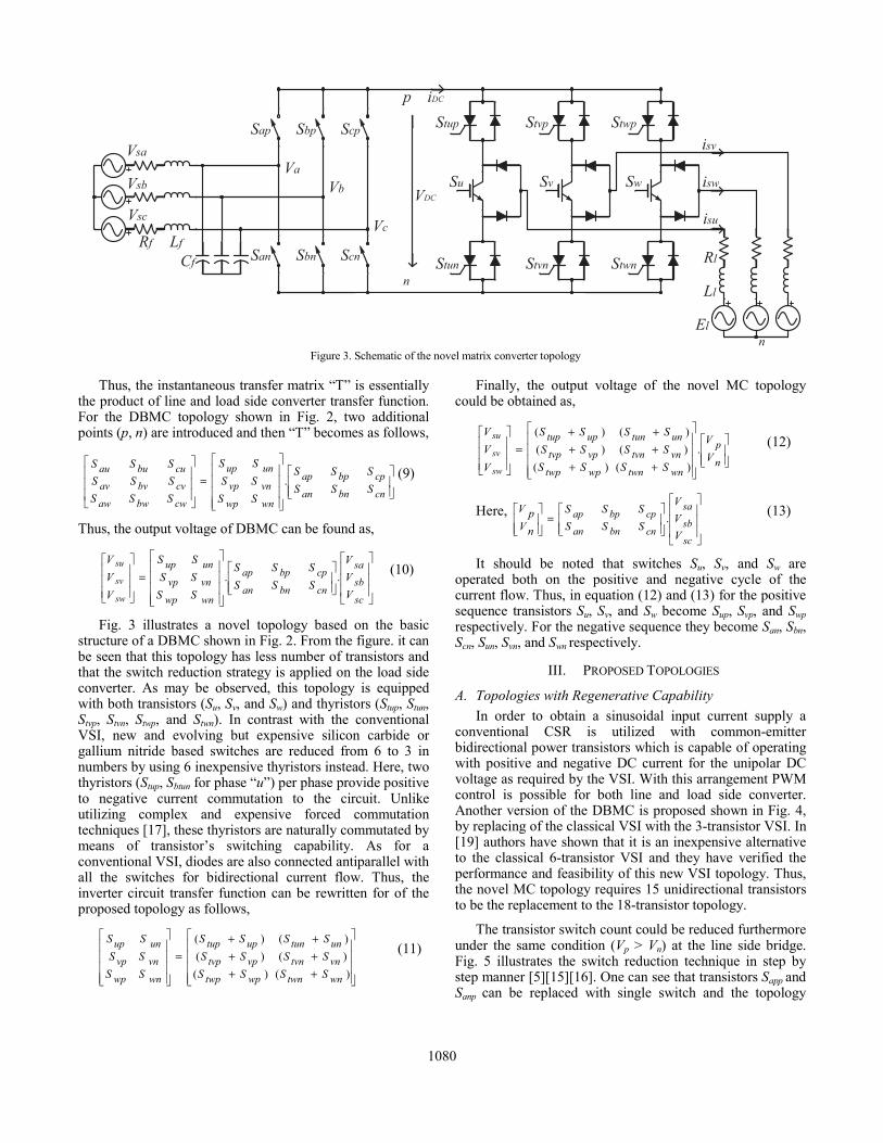
Figure 3. Schematic of the novel matrix converter topology
Stup Stvp Stwp
Stun Stvn Stwn
Su Sv Sw
p iDC
n
Rl
Ll
El
isv
isu
isw
Sap Sbp Scp
San Sbn Scn
VDC
n
Vsb
Vsa
Vsc
Rf Lf Cf
Va Vb
Vc
Thus, the instantaneous transfer matrix “T” is essentially the product of line and load side converter transfer function. For the DBMC topology shown in Fig. 2, two additional points (p, n) are introduced and then “T” becomes as follows,
⎥⎥⎦
⎤
⎢⎢⎣
⎡
⎥⎥⎥⎥
⎦
⎤
⎢⎢⎢⎢
⎣
⎡
=⎥⎥⎥
⎦
⎤
⎢⎢⎢
⎣
⎡
cn
cp
bn
bp
an
ap
wnwp
vnvp
unup
cwbwaw
cvbvav
cubuau
SS
SS
SS
SS SS SS
SSSSSSSSS
. (9)
Thus, the output voltage of DBMC can be found as,
⎥⎥⎥
⎦
⎤
⎢⎢⎢
⎣
⎡
⎥⎥⎦
⎤
⎢⎢⎣
⎡
⎥⎥⎥⎥
⎦
⎤
⎢⎢⎢⎢
⎣
⎡
=⎥⎥⎥
⎦
⎤
⎢⎢⎢
⎣
⎡
sc
sb
sa
cn
cp
bn
bp
an
ap
wnwp
vnvp
unup
VVV
SS
SS
SS
SS SS SS
VVV
sw
sv
su.. (10)
Fig. 3 illustrates a novel topology based on the basic structure of a DBMC shown in Fig. 2. From the figure. it can be seen that this topology has less number of transistors and that the switch reduction strategy is applied on the load side converter. As may be observed, this topology is equipped with both transistors (Su, Sv, and Sw) and thyristors (Stup, Stun, Stvp, Stvn, Stwp, and Stwn). In contrast with the conventional VSI, new and evolving but expensive silicon carbide or gallium nitride based switches are reduced from 6 to 3 in numbers by using 6 inexpensive thyristors instead. Here, two thyristors (Stup, Sbtun for phase “u”) per phase provide positive to negative current commutation to the circuit. Unlike utilizing complex and expensive forced commutation techniques [17], these thyristors are naturally commutated by means of transistor’s switching capability. As for a conventional VSI, diodes are also connected antiparallel with all the switches for bidirectional current flow. Thus, the inverter circuit transfer function can be rewritten for of the proposed topology as follows,
⎥⎥⎥⎥
⎦
⎤
⎢⎢⎢⎢
⎣
⎡
++++++
=
⎥⎥⎥⎥
⎦
⎤
⎢⎢⎢⎢
⎣
⎡
)()()()()()(
wntwnwptwp
vntvnvptvp
untunuptup
wnwp
vnvp
unup
SS SSSS SSSS SS
SS SS SS
(11)
Finally, the output voltage of the novel MC topology could be obtained as,
⎥⎥⎦
⎤
⎢⎢⎣
⎡
⎥⎥⎥⎥
⎦
⎤
⎢⎢⎢⎢
⎣
⎡
++++++
=⎥⎥⎥
⎦
⎤
⎢⎢⎢
⎣
⎡
n
p
wntwnwptwp
vntvnvptvp
untunuptup
VV
SS SSSS SSSS SS
VVV
sw
sv
su.
)()()()()()(
(12)
Here, ⎥⎥⎥
⎦
⎤
⎢⎢⎢
⎣
⎡
⎥⎥⎦
⎤
⎢⎢⎣
⎡=
⎥⎥⎦
⎤
⎢⎢⎣
⎡
sc
sb
sa
cn
cp
bn
bp
an
ap
VVV
SS
SS
SS
nVpV
. (13)
It should be noted that switches Su, Sv, and Sw are operated both on the positive and negative cycle of the current flow. Thus, in equation (12) and (13) for the positive sequence transistors Su, Sv, and Sw become Sup, Svp, and Swp respectively. For the negative sequence they become San, Sbn, Scn, Sun, Svn, and Swn respectively.
III. PROPOSED TOPOLOGIES
A. Topologies with Regenerative Capability In order to obtain a sinusoidal input current supply a
conventional CSR is utilized with common-emitter bidirectional power transistors which is capable of operating with positive and negative DC current for the unipolar DC voltage as required by the VSI. With this arrangement PWM control is possible for both line and load side converter. Another version of the DBMC is proposed shown in Fig. 4, by replacing of the classical VSI with the 3-transistor VSI. In [19] authors have shown that it is an inexpensive alternative to the classical 6-transistor VSI and they have verified the performance and feasibility of this new VSI topology. Thus, the novel MC topology requires 15 unidirectional transistors to be the replacement to the 18-transistor topology.
The transistor switch count could be reduced furthermore under the same condition (Vp > Vn) at the line side bridge. Fig. 5 illustrates the switch reduction technique in step by step manner [5][15][16]. One can see that transistors Sapp and Sanp can be replaced with single switch and the topology
1080

Figure 4. Novel 15-transistor MC topology
Figure 5. Transistor reduction stretegy
Figure 6. Schemetic of the novel 12-transistor MC topology
Sapn Sbpn Scpn
Sapp Sbpp Scpp
Sanp Sbnp Scnp
Sann Sbnn Scnn
Vsa
Vsb
Vsc
Rf Lf
Cf
Stup Stvp Stwp
Stun Stvn Stwn
Su Sv Sw
p idc
n
Vdc
Rl
Ll
El
Va Vb Vc
isu isv isw
n
Sapn Sbpn
Sapp Sbpp
Sanp Sbnp
Sann Sbnn
Sap
Sa
Sbp
p iDC p iDC p iDC
n n n
Vsa
Vsb
Vsc
Rf Lf
Cf
P iDC
n
VDC
Sap Sbp Scp
Sa Sb Sc
San Sbn Scn
Stup Stup Stwp
Stun Stvn Stwn
Su Sv Sw
Rl
Ll
El
Figure 7. Novel 9-transistor VSMC topology
Figure 8. Novel 9-transistor ILMC topology
Figure 9. 11-transistor ILMC topology
Figure 10. Schemetic of the novel 6-transistor MC topology
isu uisw wisv v
abc
p iDC
VDC
n
abc
isu u
isw w
isv v
p iDC
VDC
n
abc
isu u
isw w
isv v
p iDC
VDC
n
Stup Stvp Stwp
Stun Stvn Stwn
Sa Sb Sc Su Sv Sw
isu isv isw
Rl
Ll
El
Vsa
Vsb
Vsc
Rf Lf
Cf
P iDC
n
VDC
n
Cc RcCc
possesses the same performance as CMS. This type of MC was denoted as SMC in [15] and it requires 15 unidirectional power transistors. However, Fig. 6 illustrates another novel MC topology using the switch reduction technique and the 3-transistor VSI discussed above. This novel topology consists of only 12 unidirectional transistors having the same characteristics as the 15-transistor MC or CMS.
Furthermore, the DBMC topology could reduce its power transistor count by employing zero DC link current commutation technique at the line side converter as shown in Fig. 7. This strategy of switch reduction is proposed in [15][16] and denoted as VSMC or 12-transistor MC. Nevertheless, this MC topology could be replaced by the novel 9-transistor MC topology shown in Fig. 7 which resembles the same characteristics as the 12-transistor VSMC.
B. Topologies with Non-regenerative Capability With the condition iDC ≥ 0, further switch reduction could
be achieved by connecting a conventional 6-transistor CSR
and VSI in series, as a result of a 12-transistor MC [15][16] (Fig. 8). By using the same strategy described above, this topology could be substituted by the novel 9-transistor MC topology shown in Fig. 8. Here, the bidirectional power flow can be realized by two power transistor and two diodes placed between the CSR and VSI as shown in Fig. 9.
Finally, by utilizing a two-quadrant buck-type PWM rectifier suggested in [15][16] and the 3-transistor VSI, one could realize the DBMC with further reduced number of transistors. Where, no current flows through transistors Sjp and Sjn ( c,b,a∈j ). Thus, a new 6-transistor MC could be obtained as shown in Fig. 10.
This circuit structure of the 6-transistor MC and 9-transitor MC topologies are such that, they restrict the
1081

operation to unidirectional power flow. Andused when the value of the DC link curreequal to 0 (iDC ≥ 0). Due to this, the phasethe input voltage and current fundamental isAs a result of that, the power factor on the be always greater than 0.866. Neverthelesslow number of power transistors, this 6-tranbe of interest and in the future this novel reported in detail with experimental results.
C. Clamp Circuit Under normal or fault conditions the cl
essential component for both CMC and DBMpath for the commutation energy stored in threactance. However, in faulty condition energize the load current for the protection devices. The conventional clamp circuit of dual six-pack diode rectifiers and oneHowever, IMC topologies require a muchcircuit.
Moreover, in [15] the clamp circuit for 9-transistor MC or the USMC, is greatly simone diode and one capacitor. Likewise, a sand single capacitor (Cc) clamp circuit is u6-transistor MC as shown in Fig. 10. At stall the line side switches are on, the clamp is charged up to the maximum peak line vothe Cc shows higher voltage than the dc lHowever, to avoid high voltage spikescondition, with all the transistors off, the stoinductive load flows in to the Cc. Also, capacitor value depends on the load current,and the highest allowable capacitor voltage [
IV. COMMUTATION AND PWM CONT
For the purpose of simplified analysiscomponents Rf, Lf, and Cf are considerSwitching frequency of the rectifier side is higher than the input and output frequency. positive DC voltage is maintained by the reswitching functions, and the input voltage. Hcurrent and output voltage are determinedswitching functions and output current. Nevclamp circuit an additional damping resisparallel with the clamp capacitor (Cc) and dito minimize the fluctuations of the output wcan be considered as the conduction lcomponent.
In addition, the input source voltages cafollows,
⎪⎪⎪
⎩
⎪⎪⎪
⎨
⎧
+=
−=
=
)3
2tcos(
)3
2tcos(
tcos
i
i
i
πω
πω
ω
msc
msb
msa
VV
VV
VV
Figure 11. Six intervals of a switching cy
Figure 12. (a) Positive (b) negative switchin
d they can only be ent is positive or e displacement of s limited to ± π/6.
load side should s, because of the sistor MC should topology will be
amp circuit is an MC. It provides a he load’s leakage it serves to de-of the switching
f a CMC requires e capacitor [6]. h simpler clamp
the conventional mplified with only single diode (Dc) sed for the novel tarting point with capacitor voltage oltage. Normally, link voltage VDC. s under a fault ored energy in the
the size of the , load inductance, [6].
TROL SCHEME , values of filter red to be zero. considered much Input current and
ectifier circuit, its However, the DC d by the inverter vertheless, in the stor (Rc) is used iode (Dc) in order
waveform. This Rc losses switching
an be assumed as
(14)
And the input current equations a
⎪⎪⎪
⎩
⎪⎪⎪
⎨
⎧
++=
−+=
+=
)3
2tcos(
)3
2tcos(
)tcos(
ooi
ooi
ooi
πϕωθ
πϕωθ
ϕωθ
ow
ov
ou
Ii
Ii
Ii
The quantities Vm and I are thvoltage and output current, ωi andoutput angular frequency, finally φthe phase output current.
A. Switching Principle of the Line SThe switching sequence of the re
six intervals of the input voltage scan be observed from the Fig. 11 thphase input voltage has the higheeach interval. For example, in intervabsolute value. Furthermore, in onsequence is split into two portions voltage. In addition, in each portion
ycle of the rectifier circuit
ng technique of the inverter
are written bellow,
(15)
he maximum peak input d ω are the input and φ is the initial angle of
Side Converter ectifier circuit is based on synchronization angle. It hat, only one of the three st absolute value during
val one Vsa has the highest ne interval the switching
to maintain the DC link n the switching sequence
1082

Figure 13. (a) Naturally sampled sine-triangle PWM; (b) and (d) thyristor firing pulses and their conduction periods; (c) and (e) transistors switching
pulses
of line side transistor is fixed and the VDC is equal to one of the two highest positive line voltages.
Corresponding to Vsc, the highest absolute voltage, the largest positive line voltages are Vsa-Vsb and Vsa-Vsc. Finally, the rectifier switching state in each portion can be determined by following sequence. In portion 1, for the first 30o conduction period Sa and Sb remain turned on with Sc is turned off. Thus the DC side voltage is Vsa-Vsb. The dc link current iDC is equal to isab and –isc, and isa is zero. Again for the next 30o conduction period Sa and Sc are turned on with Sb is turned off, that makes the DC side voltage is equal to Vsa-Vsc. The basic strategy continues according to the phase order as shown in Table I. The detailed switching and PWM scheme for the load side converter can be found in [15].
TABLE I. LINE SIDE SWITCH AND DC VOLTAGE IN EACH INTERVAL
Interval
Portion 1 Portion 2 On Switch VDC On Switch VDC
1 Sb , Sa Vsa –Vsb Sc , Sa Vsa -Vsc 2 Sb , Sc Vsb -Vsc Sa , Sc Vsa -Vsc 3 Sc , Sb Vsb -Vsc Sa , Sb Vsb -Vsa
4 Sc , Sa Vsc -Vsa Sb , Sa Vsb -Vsa
5 Sa , Sc Vsc –Vsa Sb , Sc Vsc –Vsb
6 Sa , Sb Vsa -Vsb Sc , Sb Vsc -Vsb
B. Commutation of the Load Side Converter The commutation technique for the load side converter is
described in this section. For positive iu current, thyristor Stup is first turned on with Stun off. Transistor Su is then switched on and off using an appropriate PWM technique. Within this period, positive current flows through Stup, Su, D2, and Dt2 (cf. Fig. 12(a)). At the end of this positive half cycle; when current reaches zero, Stup is turned off by removing the gate signal from Su. After the recovery period of Stup, Stun is turned on with Stup remaining off. Again, for this negative half cycle Su is turned on and off using pulse width modulation. Also, in this period, negative current flows through D1, Dt1, Su, and Stun (cf. Fig. 12(b)). The basic strategy continues for the rest of the legs according to their phase order.
Similar to the classical VSI, this converter also has six active and two zero switching states. Eight switching states are given in Table II, where state 1 and 8 provide zero and the reaming states provide non-zero.
TABLE II. SWICHING STATES OF THE NOVEL TOPOLOGY
Switching state
Devices Output line voltages Stup+Sup Stup+Sup Stup+Swp Vab Vbc Vca
1 0 0 0 0 0 0 2 0 0 1 0 - VDC VDC 3 0 1 0 -VDC VDC 0 4 0 1 1 - VDC 0 - VDC 5 1 0 0 VDC 0 - VDC 6 1 0 1 VDC - VDC 0 7 1 1 0 0 VDC VDC 8 1 1 1 0 0 0
C. Sine-Trangle PWM control scheme In this section the PWM scheme of the inverter circuit
will be described. Here, naturally sampled sine-triangle PWM (ST-PWM) method was selected to analyze the 6-transistor MC topology. The ST-PWM method uses a single triangular carrier signal to compare against three sinusoidal reference waveforms displaced in time by 120o [18]. This type of modulation is generally termed double-edge naturally sampled modulation.
The equations for phase voltages using ST-PWM are given below,
⎪⎪⎪
⎩
⎪⎪⎪
⎨
⎧
+=+=
−=−=
==
)3
2tcos(MV)3
2tcos(
)3
2tcos(MV)3
2tcos(
tcosMVtcos
oDCo
oDCo
oDCo
πωπω
πωπω
ωω
mswz
msvz
msuz
VV
VV
VV (16)
The fundamental target three-phase line-line output voltages are,
⎪⎪⎪
⎩
⎪⎪⎪
⎨
⎧
+=−=
+=−=
+=−=
)6
cos(3
)6
cos(3
)6
cos(3
πω
πω
πω
tVMVVV
tVMVVV
tVMVVV
oDCsuzswzswu
oDCswzsvzsvw
oDCsvzsuzsuv
(17)
where, Vm = output voltage peak magnitude, M = modulation index = Vm/VDC, and the reference waveforms are defined by considering “z” as a fictitious DC bus center point.
For simplification, it is considered that no delay is given between the conduction periods of the per phase thyristors. That implies, the PWM switching of the transistors will also have no delay between the positive and negative current flow. In addition, the PWM pulses for any leg transistor’ (i.e. Su) are identical for both positive and negative current. Eventually the combination of these devices per phase ensures a typical 3 phase PWM control scheme.
1083

Fig. 13(a) illustrates the ST-PWmethodology by comparing triangular carsinusoidal reference waveforms for phase “switching pulses by ST-PWM method per are shown accordingly in Fig. 13(c) and thyristor firing pulses and their conduction ppictorially in Fig. 13(b) and 13(d). It is to those Fig.s, small blocks represent the firinbigger rectangular blocks denote the conducthyristors.
V. SIMULATION RESULT
Proposed 6-transistor MC topology has investigated utilizing system level sMATLAB/SIMULINK to observe its pfeasibility. The simulation software repswitches and the components as ideal. Simthe novel MC topology are illustrated in System level simulation has been perforutilizing open loop control arrangemenperformance. Simulation parameters taken shown in Table III.
TABLE III. SIMULATION PARAME
Parameter Value ParameterInput line voltage (p-p) 220 V Rectifier swit
frequency Input filter capacitance 250 μF Inverter swit
frequency Input filter inductance 220 μH Modulation
(M) Input filter resistance 0.02 Ω Load inductanceInput-output frequency 60 Hz Load resistance Clamp capacitance (Cc) 1 μF Back EMF (El)
Fig. 14(a) shows the output DC voltage circuit of the converter. From the Fig. it cansix intervals switching technique of the stable DC output voltage. Again in Fig.observe the DC current waveform with the cIt is to be noted that the switching frequencyalgorithm used for the rectifier circuit is 540with improved control scheme, better waachieved.
Fig. 14(c) depicts 3 phase output currenutilizing ST-PWM with switching frequenThe waveforms found through simulatiosinusoidal, however better performance cthrough improved or developed control sche
In Fig. 14(d) output line to line voAlthough the waveforms are slightly distortbe improved by developing or utilizing technique, and control scheme. It is to be nPWM technique cannot utilize the maximumto produce maximum peak fundamental outo the load, whereas the third harmonic injecspace vector PWM (SVPWM) gives fundamental output with better quality
Figure 14. Simulation results: (a) Output DCof the rectifier circuit iDC, (c) three phase o
voltage, (e) Input current
Figure 15. THD of the output current at 4.5 k
WM generation rrier signal to a
“a”. The resulting phase transistors 13(e). Moreover, periods are given be noted that in
ng pulses but the tion period of the
TS been extensively
simulation with performance and presents all the
mulation results of Fig. 14 and 15.
rmed extensively nt to verify its
for analysis are
ETERS
r Value tching 5400 Hz
tching 4500 Hz
index 0.8
e (Ll) 20 μH (Rl) 1 Ω
100 V (p-p)
from the rectifier n be seen that by rectifier ensures
. 14(b) one can condition iDC ≥ 0. y of the ST-PWM 00 Hz. However, aveforms can be
nt of the inverter ncy of 4500 Hz. on are not pure can be achieved eme.
oltage is shown. ted but it can also better switching
noted that the ST-m DC bus voltage utput line voltage cted ST-PWM or 15% enhanced
[15]. Fig. 14(e)
displays the waveforms of the inputV) and phase current (ia = 5 Amp) anphase regardless the load type. Thertype this converter will provide unitybecause of the line side filter, thephase voltage in this figure.
Finally Fig. 15 depicts the THDa 4500 kHz switching frequency. Bcurrent intervals needed to allow
C voltage VDC, and (b) current output current, (d) output line and voltage
kHz switching frequency of the
t phase voltage (Vsa = 220 nd they are found to be in refore, regardless the load y power factor. However, phase current leads the
D of the output current for Because of the slight zero w the thyristors recover
1084

blocking ability a slight increase in the current THD was obtained compared to the conventional inverter.
VI. CONCLUSION The focal point of this paper is developing several
attractive yet inexpensive alternative topologies at the mid to high power level system. The performance and feasibility has been substantiated with system level simulation with utilizing open loop control scheme. Performance wise it resembles conventional topologies but with certain advantages. Thus, these variations of previous topologies could be a useful alternative solution considering the attractive features provided by these topologies. They are,
• Reduction in expensive power transistor count
• High quality input and output current
• Operations with unity power factor with any load type
• Simple clamp circuit with one diode and one capacitor is required
• Practical implementation of the load side converter could provide greater DC link voltage utilization because it requires significantly less dead time. Unlike the conventional VSI this VSI requires dead times only at zero crossing instance of the output current since it consists of only one transistors per phase.
The 6-transistor and the 9-transistor MC allows uni-directional power flow due their rectifier circuit arrangement. However, its low transistor count makes the 6-transistor MC a very attractive alternative in suitable applications, such as permanent magnet motor load. Nevertheless, rest of the topologies proposed here, are capable of work in bidirectional power flow. The comparison table in terms of transistor switches of conventional DBMC and the novel topology are summarized in Table IV
TABLE IV. REALIZATION EFFORT OF DIFFERENT MC TOPOLOGIES
Converter Type Transistors Novel Topology Transistors
IMC 18 15-transistor IMC 15 SMC 15 12-transistor SMC 12 VSMC 12 9-transistor VSMC 9 ILMC 12 9-transistor ILMC 9 B-ILMC 15 11-transistor B-ILMC 11 USMC 9 6-transistor USMC 6
Furthermore, future topics of research will concern, improvement of the switching technique to improve the output and input voltage waveforms, and their transfer ratio, reduction of the harmonic contents of output waveforms. Switching losses minimization of the topologies. Moreover, utilization of a closed loop control scheme could improve the performance of the topology in all aspects. These converters and the extended multi-level topologies based on these converters can be investigated for a number of future power system applications in both medium and high power systems.
REFERENCES [1] M. Venturini, “A new sine wave in sine wave out conversion
technique which eliminates reactive elements,” Proceedings of POWERCON 7. 1980, pp. E3_1-E3_15.
[2] A. Alesina, and M. Venturini, “Solid-state power conversion: A Fourier analysis approach to generalised transformer syntheses,” IEEE Transactions on Circuits and Systems. 28. (4). April 1981, pp. 319-330.
[3] P. Wheeler, J.Rodrigues, J.C. Clare, L. Epringham, and A. Weinstein, “Matrix converters: A technology review”, IEEE Trans. On Industrial Electronics, Vol. 49, No. 2, April, 2002, pp. 276-288.
[4] Jose Rodriguez, Marco Rivera, et. al., “A review of control and modulation methods for matrix converters”, IEEE Trans. On Industrial Electronics, Vol. 59, No. 1, January, 2012, pp. 58-70.
[5] M.A. Rahim, T.C. Green, and B.W. Williams, “Three-phase step-down reversible AC-DC power converter,” Proceedings of the 26th IEEE PESC, Atlanta, USA, Vol.2, pp. 973-978, 1995.
[6] P. Nielsen, F. Blaabjerg and J. K. Pedersen, “New protection issues of a matrix converter: design considerations for adjustable speed drives”, IEEE Trans. on Industry Applications, vol. 35, No. 5, 1999, pp. 1150-1161.
[7] J.-H. Youm, and B.-H. Kwon, “Switching technique for current-controlled ac-to-ac converters,” IEEE Trans. on Industrial Electronics, vol. 46, No. 2, 1999, pp. 309-318.
[8] F. Blaabjerg, D. Casadei, C. Klumpner, and M. Matteini, “Comparison of two current modulation strategies for matrix converters under unbalanced input voltage conditions,” IEEE Trans. Ind. Electron., vol. 49, no. 2, Apr. 2002, pp. 289–296.
[9] S. Muller, U. Ammann, and S. Rees, “New time-discrete modulation scheme for matrix converters,” IEEE Trans. Ind. Electron., vol. 52, no. 6, Dec. 2005, pp. 1607–1615.
[10] M. Rivera, R. Vargas, J. Espinoza, and J. Rodriguez, “Behavior of the predictive DTC based matrix converter under unbalanced AC-supply,” in Proc. IEEE PESC., Sep. 2007, pp. 202–207.
[11] C. Klumpner, F. Blaabjerg and et. al., "A new modulation method for matrix converters", In Proceedings of IEEE Industry Applications Socieiy Conference (IAS' 200v, vol. .3, pp. 2143-2150, USA, 2001
[12] M. Muroya, K. Shinohara et. al., “Four-step commutation strategy of PWM rectifier of converter without DC link components for induction motor drive”. In Proc. IEMDC 2001, pp. 770-772.
[13] J. Holtz, and U. Boelkens, “Direct frequency converter with sinusoidal line currents for speed-variable motors”, IEEE Trans. On Industrial Electronics, vol. 36, No. 4, 1989, pp. 475-479.
[14] L. Wei, and T.A. Lipo, “A novel matrix converter with simple commutation”, In Proceedings of 36th IEEE Industry Applications Society Conference. (IAS’2001), vol.3, pp.1749-1754, IL,USA, 2001.
[15] L. Wei, and T.A. Lipo, “Matrix converter with reduced number of switches”, In Conf. Record of the 20th WEMPEC anniversary meeting, Madison, WI, USA, Oct. 24 –25th, 2001.
[16] J.W. Kolar, M. Baumann, and et. al., “Novel three-phase AC-DC-AC sparse matrix converter”, In Proceedings of 17th IEEE APEC., 2002, Vol. 2, pp. 777-791.
[17] G. K. Dubey, “Classification of thyristor commutation methods”, IEEE Trans. On Industry Applications, Vol. IA-19, No. 4, July/Aug 1983, pp. 600-606.
[18] D. G. Holmes, T. A. Lipo, “Pulse width modulation for power converters: principles and practice” (book), IEEE Press Series on Power Engineering, 2003.
[19] S. M. Sajjad Hossain Rafin, T. A. Lipo and Byung-il Kwon, “A novel topology for a voltage source inverter with reduced transistor count and utilizing naturally commutated thyristors with simple commutation,” In Proceedings of 22nd IEEE Int. Sym. on Power Electronics, Electrical Drives, Automation and Motion, SPEEDAM, Iscia, Italy, June 18-20, 2014.
1085