nonlinear optics in titanium dioxide: from bulk to integrated
TRANSCRIPT
Nonlinear optics in titanium dioxide: from bulk to integrated opticaldevices
(Article begins on next page)
The Harvard community has made this article openly available.Please share how this access benefits you. Your story matters.
Citation Evans, Christopher Courtney. 2013. Nonlinear optics in titaniumdioxide: from bulk to integrated optical devices. Doctoraldissertation, Harvard University.
Accessed May 11, 2017 10:08:11 PM EDT
Citable Link http://nrs.harvard.edu/urn-3:HUL.InstRepos:11181139
Terms of Use This article was downloaded from Harvard University's DASHrepository, and is made available under the terms and conditionsapplicable to Other Posted Material, as set forth athttp://nrs.harvard.edu/urn-3:HUL.InstRepos:dash.current.terms-of-use#LAA
Nonlinear optics in titanium dioxide: from bulk tointegrated optical devices
A thesis presented
by
Christopher Courtney Evans
to
The School of Engineering and Applied Sciences
in partial fulfillment of the requirements
for the degree of
Doctor of Philosophy
in the subject of
Applied Physics
Harvard University
Cambridge, Massachusetts
August 2013

©2013 - Christopher Courtney Evans
All rights reserved.
Thesis advisor Author
Eric Mazur Christopher Courtney Evans
Nonlinear optics in titanium dioxide: from bulk to integrated
optical devices
AbstractIn this thesis, we explore titanium dioxide (TiO2) for ultrafast, on-chip nonlinear
optics by studying it in bulk, thin films, and in integrated nonlinear optical devices.
TiO2’s large nonlinear index of refraction (30 times that of silica) and low two-photon
absorption can enable all-optical switching, logic, and wavelength conversion across
wavelengths spanning the telecommunications octave (800–1600 nm). In addition,
its high linear index of refraction can enhance optical confinement down to nano-
scale dimensions and facilitate the tight waveguide bends necessary for dense on-chip
integration. Throughout this thesis, we develop TiO2 as a novel on-chip nonlinear
optics platform.
We begin by studying nonlinear refraction and multiphoton absorption in bulk
rutile TiO2 using the Z-scan technique. We quantify nonlinear refraction and mixed
two- and three-photon absorption near TiO2’s half-bandgap (800 nm). This data
shows that we can avoid parasitic two-photon absorption by operating at wavelengths
longer than 813 nm.
Planar integrated photonic devices require high-quality thin films that can act
as low-loss planar waveguides. We deposit thin films of TiO2 on oxidized silicon
wafers using reactive sputtering of titanium metal in an oxygen environment. Our
iii
optimized amorphous and polycrystalline anatase TiO2 thin films have high refractive
indices from 2.4–2.8 at visible wavelengths and planar waveguiding losses as low as
0.4 dB/cm (826 nm).
Using electron-beam lithography, we structure these films to fabricate waveg-
uides with sub-micron features. We quantify propagation losses at wavelengths from
633 to 1550 nm and observe losses as low as 4 dB/cm. Next, we demonstrate devices
including bends, directional couplers, and racetrack resonators that form the basic
building-blocks for more advanced photonic devices.
Finally, we observe the first nonlinear optics in integrated TiO2 waveguides. By
measuring the spectral broadening of femtosecond pulses in TiO2, we quantify the
nonlinear index of anatase TiO2 around 1565 and 794 nm. In addition, we explore
stimulated Raman scattering and third-harmonic generation in our waveguides. With
this first demonstration of an integrated nonlinear optical device in TiO2, we conclude
that TiO2 is a viable and promising material for all-optical applications.
iv
Contents
Title Page . . . . . . . . . . . . . . . . . . . . . . . . . . . . . . . . . . . . iAbstract . . . . . . . . . . . . . . . . . . . . . . . . . . . . . . . . . . . . . iiiTable of Contents . . . . . . . . . . . . . . . . . . . . . . . . . . . . . . . . vCitations to previously published work . . . . . . . . . . . . . . . . . . . . viiiAcknowledgments . . . . . . . . . . . . . . . . . . . . . . . . . . . . . . . . ixDedication . . . . . . . . . . . . . . . . . . . . . . . . . . . . . . . . . . . . xiv
1 Introduction 11.1 Organization of the dissertation . . . . . . . . . . . . . . . . . . . . . 3
2 Linear and nonlinear optics 62.1 Linear optics . . . . . . . . . . . . . . . . . . . . . . . . . . . . . . . 6
2.1.1 Plane waves . . . . . . . . . . . . . . . . . . . . . . . . . . . . 72.1.2 Dielectric function . . . . . . . . . . . . . . . . . . . . . . . . 112.1.3 Pulse propagation . . . . . . . . . . . . . . . . . . . . . . . . . 172.1.4 Temporal pulse broadening . . . . . . . . . . . . . . . . . . . . 21
2.2 Nonlinear optics . . . . . . . . . . . . . . . . . . . . . . . . . . . . . . 282.2.1 Nonlinear polarization . . . . . . . . . . . . . . . . . . . . . . 282.2.2 Nonlinear index of refraction . . . . . . . . . . . . . . . . . . . 332.2.3 Self-phase modulation effects . . . . . . . . . . . . . . . . . . . 37
2.3 Nonlinear optics at the nanoscale . . . . . . . . . . . . . . . . . . . . 432.3.1 Waveguides . . . . . . . . . . . . . . . . . . . . . . . . . . . . 442.3.2 Nonlinear pulse propagation . . . . . . . . . . . . . . . . . . . 562.3.3 Nonlinear properties of silica nanowires . . . . . . . . . . . . . 64
2.4 Summary . . . . . . . . . . . . . . . . . . . . . . . . . . . . . . . . . 66
3 Nonlinearities in bulk rutile TiO2 683.1 The Z-scan technique . . . . . . . . . . . . . . . . . . . . . . . . . . . 69
3.1.1 Closed-aperture Z-scan analysis . . . . . . . . . . . . . . . . . 713.1.2 Open-aperture Z-scan analysis . . . . . . . . . . . . . . . . . . 76
3.2 Nonlinear refraction in bulk rutile TiO2 . . . . . . . . . . . . . . . . . 79
v
Contents
3.2.1 Introduction . . . . . . . . . . . . . . . . . . . . . . . . . . . . 793.2.2 Experimental . . . . . . . . . . . . . . . . . . . . . . . . . . . 813.2.3 Analysis methods . . . . . . . . . . . . . . . . . . . . . . . . . 823.2.4 Results and analysis . . . . . . . . . . . . . . . . . . . . . . . 833.2.5 Discussion . . . . . . . . . . . . . . . . . . . . . . . . . . . . . 853.2.6 Nonlinear refraction summary . . . . . . . . . . . . . . . . . . 87
3.3 Multiphoton absorption in bulk rutile TiO2 . . . . . . . . . . . . . . . 873.3.1 Introduction . . . . . . . . . . . . . . . . . . . . . . . . . . . . 883.3.2 Experimental . . . . . . . . . . . . . . . . . . . . . . . . . . . 903.3.3 Results and discussion . . . . . . . . . . . . . . . . . . . . . . 923.3.4 Conclusion . . . . . . . . . . . . . . . . . . . . . . . . . . . . . 1033.3.5 Acknowledgements . . . . . . . . . . . . . . . . . . . . . . . . 103
4 Optimizing TiO2 thin films 1054.1 Experimental . . . . . . . . . . . . . . . . . . . . . . . . . . . . . . . 106
4.1.1 Characterization methods . . . . . . . . . . . . . . . . . . . . 1064.2 Results and discussion . . . . . . . . . . . . . . . . . . . . . . . . . . 109
4.2.1 The effects of deposition temperature on film crystallinity . . . 1094.2.2 Optimizing amorphous TiO2 films . . . . . . . . . . . . . . . . 1114.2.3 Optimizing anatase TiO2 films . . . . . . . . . . . . . . . . . . 114
4.3 Conclusion . . . . . . . . . . . . . . . . . . . . . . . . . . . . . . . . . 116
5 Linear optical properties of integrated TiO2 waveguides and devices1185.1 Linear waveguides . . . . . . . . . . . . . . . . . . . . . . . . . . . . . 118
5.1.1 Introduction . . . . . . . . . . . . . . . . . . . . . . . . . . . . 1195.1.2 TiO2 thin films . . . . . . . . . . . . . . . . . . . . . . . . . . 1225.1.3 Submicrometer-wide TiO2 waveguides . . . . . . . . . . . . . . 1265.1.4 TiO2 microphotonic features . . . . . . . . . . . . . . . . . . . 1285.1.5 Discussion . . . . . . . . . . . . . . . . . . . . . . . . . . . . . 1335.1.6 Conclusion . . . . . . . . . . . . . . . . . . . . . . . . . . . . . 136
5.2 Racetrack resonators for visible photonics . . . . . . . . . . . . . . . . 137
6 Nonlinear properties of TiO2 waveguides 1466.1 Spectral broadening . . . . . . . . . . . . . . . . . . . . . . . . . . . . 146
6.1.1 Introduction . . . . . . . . . . . . . . . . . . . . . . . . . . . . 1476.1.2 Experimental Procedure . . . . . . . . . . . . . . . . . . . . . 1506.1.3 Numerical simulation . . . . . . . . . . . . . . . . . . . . . . . 1526.1.4 Experimental and simulation results . . . . . . . . . . . . . . . 1556.1.5 Discussion . . . . . . . . . . . . . . . . . . . . . . . . . . . . . 1586.1.6 Conclusion . . . . . . . . . . . . . . . . . . . . . . . . . . . . . 162
6.2 Third-harmonic generation . . . . . . . . . . . . . . . . . . . . . . . . 1636.2.1 Third-harmonic generation in multimode waveguides . . . . . 164
vi

Contents
6.2.2 Experimental . . . . . . . . . . . . . . . . . . . . . . . . . . . 1686.2.3 Results . . . . . . . . . . . . . . . . . . . . . . . . . . . . . . . 1696.2.4 Discussion . . . . . . . . . . . . . . . . . . . . . . . . . . . . . 1726.2.5 Conclusion . . . . . . . . . . . . . . . . . . . . . . . . . . . . . 176
7 Conclusions and outlook 177
A Z-scan model for mixed two- and three- photon absorption 184
B Photodarkening in amorphous TiO2 films 187B.1 Standard Z-scan measurements . . . . . . . . . . . . . . . . . . . . . 188
B.1.1 Experimental . . . . . . . . . . . . . . . . . . . . . . . . . . . 188B.1.2 Results and analysis . . . . . . . . . . . . . . . . . . . . . . . 189B.1.3 Discussion . . . . . . . . . . . . . . . . . . . . . . . . . . . . . 192
B.2 Time-dependent photodarkening . . . . . . . . . . . . . . . . . . . . . 193B.2.1 Experiment . . . . . . . . . . . . . . . . . . . . . . . . . . . . 193B.2.2 Results and analysis . . . . . . . . . . . . . . . . . . . . . . . 193B.2.3 Discussion . . . . . . . . . . . . . . . . . . . . . . . . . . . . . 194
B.3 Thermal nonlinearities in photodarkened amorphous TiO2 . . . . . . 196B.3.1 Experiment . . . . . . . . . . . . . . . . . . . . . . . . . . . . 196B.3.2 Results and analysis . . . . . . . . . . . . . . . . . . . . . . . 197B.3.3 Discussion . . . . . . . . . . . . . . . . . . . . . . . . . . . . . 199
B.4 Conclusion . . . . . . . . . . . . . . . . . . . . . . . . . . . . . . . . . 200
C Simulation of TiO2-based Sagnac interferometers 202C.1 Sagnac interferometers . . . . . . . . . . . . . . . . . . . . . . . . . . 203C.2 Analysis of a Sagnac interferometer . . . . . . . . . . . . . . . . . . . 205C.3 All-optical switching . . . . . . . . . . . . . . . . . . . . . . . . . . . 209C.4 All-optical logic . . . . . . . . . . . . . . . . . . . . . . . . . . . . . . 210C.5 Pulse propagation in a nonlinear Sagnac interferometer . . . . . . . . 212C.6 All-optical switching in TiO2 waveguides . . . . . . . . . . . . . . . . 216C.7 Conclusion . . . . . . . . . . . . . . . . . . . . . . . . . . . . . . . . . 217
Bibliography 219
vii

Citations to previously published work
Parts of this dissertation cover research reported in the following articles:
1. C. C. Evans and E. Mazur, "Nanophotonics: Linear and nonlinear optics at
the nanoscale", in Nano-Optics for Enhancing Light-Matter Interactions on a
Molecular Scale: Plasmonics, Photonic Materials and Sub-Wavelength Resolu-
tion, edited by B. Di Bartolo and J. Collins (Springer London, Limited, 2012).
2. C. C. Evans, J. D. B. Bradley, E. A. Martí-Panameño, and E. Mazur, "Mixed
two- and three-photon absorption in bulk rutile (TiO2) around 800 nm," Optics
Express, 20 (3), 3118-3128, 2012.
3. C. C. Evans, K. Shtyrkova, J. D. B. Bradley, O. Reshef, E. Ippen, and E. Mazur,
"Spectral broadening in anatase titanium dioxide waveguides at telecommuni-
cation and near-visible wavelengths," Optics Express, 21 (15), 18582-18591,
2013.
4. J. D. B. Bradley, C. C. Evans, J. T. Choy, O. Reshef, P. B. Deotare, F. Parsy,
K. C. Phillips, M. Lončar, and E. Mazur, "Submicrometer-wide amorphous
and polycrystalline anatase TiO2 waveguides for microphotonic devices," Optics
Express, 20 (21), 23821-23831, 2012.
5. J. T. Choy, J. D. B. Bradley, P. B. Deotare, I. B. Burgess, C. C. Evans, E.
Mazur, and M. Lončar, "Integrated TiO2 resonators for visible photonics," Op-
tics Letters, 37 (4), 539-541, 2012.
viii

Acknowledgments“Listen Lad, I’ve built this kingdom up from nothin’. When I startedhere, all there was was swamp. Everyone said I was daft to build acastle on a swamp, but I built it all the same, just to show ’em! It sankinto the swamp, so... I built a second one... that sank into the swamp...so I built a third one... That burned down, fell over, then sank into theswamp, but the fourth one STAYED UP! And that’s what you’re goingto get, Lad, the strongest castle in these islands.”
The King of the Swamp Castle, Monty Python and the Holy Grail
Success in research and in life often requires failure, however, I have been very
lucky to have a network of people who have helped me navigate and persevere through
these pitfalls to find success and fulfilment in science. I am very thankful for countless
people who helped me find my way to graduate school and the many more that helped
me get through it.
Getting to graduate school has been a long journey that was only possible
thanks to many amazing mentors. Early on, my uncle Steve encouraged creativity and
inquiry through lively debate. Equally inspiring was my uncle Charlie, who possessed
unbounded knowledge and had the patience to explain population inversion to a
curious 10 year old. At the end of high school before I headed off to pursue a music
career, my math teacher, Mr. Kaczowka, reminded me to “keep up with calculus”. I
had many mentors when I was learning to become a recording engineering, including
Mark Wessel, Carl Beatty, Will Sandalls, and Jesse Henderson. They helped me
develop the confidence, independence, eyes and ears for detail, and the “whatever
it takes” attitude that has stayed with me throughout graduate school. When I
began repairing audio equipment, Bill Gitt and Burt Price helped me develop trouble-
shooting skills and introduced me to “The Art of Electronics”, which later enticed
me to study electrical engineering at the University of Massachusetts, Lowell. I am
ix

Acknowledgments
deeply indebted to my physics professors David Pullen, Kunnat Sebastian, Robert
Giles, and Albert Altman at UMass Lowell for reawakening the passion for physics
that I had forgotten about since high school. The focus and follow-through I learned
in music, powered by my revitalized excitement for physics, lead me to pursue a PhD
at Harvard, thanks to all of my mentors along the way.
I would like to thank Eric Mazur for giving me such a wonderful opportunity
to work in his group. Eric has given me the freedom and responsibility to plan and
execute my research that, with his encouragement and respect, has developed my
skill and self-confidence as a researcher. Eric’s elegance for presentations has allowed
me to study the “magic” he brings to what could be a dry scientific talk. Eric has
also been a great friend outside of the lab. We have shared many adventures from
mountain biking and hiking to cross-country skiing, and we managed to squeeze in
the occasional squash game into our busy schedules. As I go forth and explore new
directions, I realize and appreciate how much Eric has helped me grow both as a
scientist and as a person.
My adjustment to the research and lifestyle at Harvard was made easier by all
of the senior students and postdocs. First, I want to thank Jonathan Bradley for
the dedication, and push that made this work successful. I am truly grateful for his
guidance and his friendship. Many senior students reminded me to focus on the bigger
picture: Sam Chung (for giving me “the speech”), Tina Shih (for reminding me that
“reviewers will just get lost in too many details”), Eric Diebold (for his “go big or go
home” attitude), and Paul Peng (my Photonics West “roomie”, who demonstrates the
value of keeping an open mind). Additionally, Rafael Gattass, Geoff Svacha, Mark
x

Acknowledgments
Winkler, Prakriti Tayalia, and Jessica Watkins provided a warm welcome and were
exemplary role models. I would also like to thank the many postdocs within the
Mazur Group: Julie Schell (for conversations that “go a little too far”), Laura Tucker
(for reminding me of my music beginnings), Jin Suntivich (for the amazing scientific
discussions), and Valeria Nuzzo (for telling me to “just graduate”).
I feel I could not have made it through without the support and friendship of
every member of the Mazur Group. I would like to thank all of my peers including
Jason Dowd (for switching projects), Kevin Vora (for all the help figuring out various
optical toys), and Renee Sher (my go-to person for advice). I have had a lot of fun
learning what it means to be a graduate student from such a great group of mentors
and peers. I also greatly appreciate the younger students and visitors who have made
life in the lab fun: Sally Kang (“um ma!”), Yu-Ting Lin (for the occasional help
writing text messages), Michael Moebius (for being a good sport, “Mickey”), Kasey
Phillips (for all the writing help and for organizing impromptu group activities), Phil
Munoz (for making the Mazur Group men look classy), Kelly Miller (“Squaaasssh!!”),
Ben Franta (for all the adventures), Orad Reshef (for singing about his dislike for
e-beam), Sarah Greisse-Nascimento (for the colorful nickname), Guoliang Deng (for
all the spicy food), Nabiha Saklayen (for bringing an upbeat attitude to the lab),
Fauzy Wan (for all the squash), Erwin Marti (mi amigo), Markus Pollnau (for the
music in “The Marsala Room”), Virginia Casas (for being on top of all the details),
and Sebastien Courvoisier (for making the office sound like an airport). I will truly
treasure all of the memories, from Erice to hiking, skiing, mountain biking, canoeing,
and squash. I am honored to say the Mazur Group has been my family throughout
xi

Acknowledgments
graduate school. I could not ask to be surrounded by a better group of people.
This research would not be possible without the extended nanophotonics team.
I owe the silica nanowire team a great amount of thanks as their work directly in-
spired this research: Limin Tong, Rafael Gattass, Geoff Svacha, and Jason Dowd.
It has been an honor to collaborate with so many great professors: Marko Loncar,
Markus Pollnau, Erwin Marti, Erich Ippen, Anming Hu, Tobias Voss, and Hamed
Majedi. I want to thank all of the students and postdocs who helped pioneer this
work (Jennifer Choy, Jonathan Bradley, Parag Deotare, Ruwan Senaratne, Kasey
Phillips, and Ian Burgess) and everyone else who helped realize its potential (Fran-
cois Parsy, Orad Reshef, Katia Shtyrkova, and Michael Moebius). I would also like
to recognize all of the undergraduate students who have supported my research over
the years: Lili Jiang, Grisel Rivera Batista, Stephanie Swartz, Vivek Thacker, and
Cavanaugh Welch. These last few months have been a fun and dynamic time for re-
search, thanks to the unique makeup of our extended subgroup. Orad’s creativity and
passion to realize actual devices has allowed him to persevere, even when banished to
the cleanroom. Michael’s curiosity, versatility, and camaraderie have helped me see
the forest through the trees. Katia’s skill, excitement, and unbounded dedication to
“getting it right” reminds me of my favorite recording sessions that were so electrify-
ing, the energy kept us working well into the next morning. Although she has just
joined, working with Sarah has been fantastic and I am excited to see where her fresh
perspective, dependability, and eagerness to learn will take her. Finally, I would like
to say that I am thrilled for the next generation of the nanophotonics team and wish
them continued success.
xii

Acknowledgments
Lastly, and most importantly, I would like to thank my family. I am very
fortunate to have parents who are so supportive of all the different directions I have
taken. I am also extremely grateful for my wife, Lesley. She has been an amazing
partner whose support and understanding has allowed me to follow my passions. I
have always believed life is not a straight line. My winding journey to graduate school
is a testament to this belief, and has only been possible and enjoyable thanks to a
near countless number of people, for whom I am deeply indebted.
Christopher C. Evans
Cambridge, Massachusetts
September, 2013
Acknowledgements of Financial Support
The research described in this thesis was supported by the National Science Foun-
dation under contracts ECCS-0901469 and ECCS-1201976, by the MRSEC Program
of the National Science Foundation under contract DMR-0819762, with additional
funding from the Harvard Quantum Optics Center.
xiii

To my family.
xiv
Chapter 1
Introduction
As the information age progresses, our demand for telecommunications bandwidth
and computing power continues to skyrocket. By 2020, the demand for single-channel
bandwidth is predicted to exceed 1 Tb/s [1]. Such high bitrates will require process-
ing ultrafast optical signals. One potential solution is to use all-optical processing to
avoid the speed limitations imposed by electron transport times in conventional op-
toelectronic devices. An ideal photonic material should enable ultrafast optical signal
processing from the interconnect band (800–900 nm) to telecommunications bands
(1300–1600 nm). Additionally, integration of such a material will enable a compact,
low-cost, mass-producible solution that can be further integrated with other electronic
and photonic components, all on a chip. To achieve these goals, we seek to push the
boundaries of ultrafast devices by developing a new integrated photonics medium:
titanium dioxide (TiO2).
While promising all-optical devices have been demonstrated using current ma-
terials [2–5], most nonlinear photonic materials suffer from a variety of limiting fac-
1

Chapter 1: Introduction
tors [6]. These limitations include: high materials cost (III-V semiconductors), poor
stability (polymers), large device size due to low nonlinearity and low refractive index
contrast (various glasses), high linear absorption (plasmonic materials), high multi-
photon absorption (silicon [7]), and low maximum operating intensities (chalcogenide
glasses [8]). In addition, nearly all of these technologies address the 1.5-µm telecom-
munications band exclusively and neglect wavelengths around 1300 nm as well as the
interconnect band (800–900 nm). We see an imminent need for a novel integrated
material that overcomes many of these limits and bridges the gap between these
communication bands.
Ultrafast all-optical processing demands a near-instantaneous material response.
For bit rates greater than 1 Tb/s, this is currently only achievable with passive,
non-resonant nonlinearities such the electronic Kerr effect. Therefore, the goal is to
maximize the Kerr nonlinearity while minimizing parasitic two-photon absorption.
Given that the onset of two-photon absorption occurs at 2~ω = Eg [9] and the
nonlinearity in semiconductors scales at E−4g [10], the solution is simple: choose a
material with a bandgap energy that is just over twice the single photon energy. For
operation from 800–1600 nm, these scaling rules suggests a bandgap energy of 3.1 eV.
Titanium dioxide’s band gap of 3.1 eV provides transparency throughout the
visible spectrum and ultrafast all-optical capabilities for wavelengths greater than 800
nm. It has a high nonlinear refractive index that is 30 times silica, with vanishing
two-photon absorption around 800 nm [11]. Its high linear refractive index (2.4–2.8)
enables dense on-chip integration of nanophotonic waveguides, adaptable waveguide
dispersion, and high confinement. This high confinement produces effective nonlin-
2
Chapter 1: Introduction
earities up to 100,000 times that found in standard silica fiber. By exploiting the
ultrafast nonlinear Kerr effect in TiO2, our devices can achieve theoretical bitrates
in excess of 1 Tb/s. In addition, TiO2 is inexpensive, abundant, and nontoxic. By
using deposited TiO2 and conventional fabrication procedures, we present a scalable
technology that is readily integrated into electronic or other photonic systems. These
properties make TiO2 an excellent candidate material for all-optical processing.
In this thesis, we explore and develop integrated TiO2 devices for nonlinear
optical applications. We first gain insight into the nonlinear properties of TiO2 by
studying the bulk material near its half-bandgap (800 nm). Next, we develop and
characterize thin films of TiO2. Using these films, we form waveguides and then
demonstrate several linear optical building-block devices. Finally, we characterize
the nonlinear optical properties of integrated TiO2 waveguides and compare with
our bulk measurements. By developing and exploring this novel photonic material,
we demonstrate that TiO2 is a promising material platform for integrated nonlin-
ear optics at wavelengths ranging from the interconnect band (800–900 nm) to the
telecommunication band (1300–1600 nm).
1.1 Organization of the dissertation
We introduce TiO2 by first studying the bulk material, then we optimize thin-films to
serve as a preform for devices, and lastly, we develop and explore integrated nanowire
devices.
Chapter 2 serves as an basic introduction to linear and nonlinear optics of bulk
materials. This lays the foundation for all the work covered in this thesis. We discuss
3
Chapter 1: Introduction
how to evaluate a potential nonlinear optical material using nonlinear coefficients.
Next, we show the additional control that nanoscale structure can have for nonlinear
optical applications. To demonstrate these principles, we summarize previous work
using silica nanowires.
Chapter 3 explores the nonlinear properties of bulk rutile TiO2 around its half-
bandgap (800 nm) using the Z-scan technique. We first describe the experimental
and analytical methods, then present two studies. The first study measures nonlinear
refraction, then the second quantifies mixed two- and three-photon absorption.
Chapter 4 summarizes a series of deposition studies to develop high-quality
thin films suitable for device fabrication. This results in two varieties of TiO2 films,
depending on the deposition temperature. Lower temperature results in amorphous
TiO2; at higher temperature, we obtain polycrystalline anatase.
Chapter 5 uses these thin films to fabricate waveguides. Using these waveguides,
we explore their linear optical properties. Lastly, we form them into basic devices
including bends, directional couplers, and racetrack resonators.
Chapter 6 reports on the nonlinear properties of polycrystalline anatase waveg-
uides. Nonlinear effects include spectral broadening, stimulated Raman scattering,
and third-harmonic generation.
Chapter 7 concludes this thesis and presents an outlook for the future of TiO2
photonics.
Appendix A describes a theoretical model we developed to extract mixed two-
and three-photon absorption coefficients from open-aperture Z-scan measurements.
Appendix B presents a preliminary study of photodarkening of amorphous TiO2
4

Chapter 1: Introduction
thin films using femtosecond pulses around 800 nm.
Appendix C presents the nonlinear Sagnac interferometer as a promising device
for all-optical modulation, switching, and logic. In this section, we present the basic
theory of nonlinear Sagnac interferometers. We conclude with simulation results
using theoretically and experimentally obtained parameters for TiO2 and present key
milestones necessary to achieve full modulation in a Sagnac interferometer.
5

Chapter 2
Linear and nonlinear optics
Light propagation in sub-wavelength waveguides enables tight confinement over long
propagation lengths to enhance nonlinear optical interactions. Not only can sub-
wavelength waveguides compress light spatially, they also provide a tunable means
to control the spreading of light pulses in time, producing significant effects even
for small pulse energies. By exploring linear and nonlinear light propagation, first
for free-space conditions, then for sub-wavelength guided conditions, we demonstrate
how sub-wavelength structure can enhance nonlinear optics at the nanoscale.
2.1 Linear optics
We begin by developing a fundamental understanding of light propagation in materials
that we will build upon as we cover linear and nonlinear light propagation in nano-
scale structures. We introduce plane-wave propagation in bulk materials and develop
a simple model to explain the frequency dependence of the dielectric function. We
6

Chapter 2: Linear and nonlinear optics
observe how this frequency dependence affects optical pulse propagation. With this
foundation, we will later explore nonlinear optics in TiO2.
2.1.1 Plane waves
Throughout this chapter, we will develop and use several different wave equations.
Each wave equation makes assumptions to localize energy both in time, using pulses,
and in space, using waveguides. The first wave equation assumes plane waves at a
single frequency (continuous wave). To localize in time, an optical pulse requires the
interference of multiple frequencies. Therefore, we model a pulse as a single frequency
modulated by an envelope function using the slowly varying envelope approximation
(SVEA). We use waveguides to confine light spatially by taking advantage of sus-
tained propagating solutions of Maxwell’s equations, known as modes. Light guided
within a mode propagates in an analogous way to plane waves using the guided-wave
equation. Finally, we will augment this equation using the SVEA to form a fourth
wave equation to describe pulses in waveguides. Strong light-matter interactions cre-
ate a nonlinear polarization that we must include. We will introduce the physics
of nonlinear optics in the simplest way possible, using plane waves. Lastly, we will
modify the pulsed waveguide equation to include third-order nonlinear optical effects
to form the Nonlinear Schroedinger Equation (NLSE).
7
Chapter 2: Linear and nonlinear optics
Wave equation for plane waves
We start with Maxwell’s equations in a linear, homogeneous material with no free
charges or currents:
(i) ~∇ · ~E = 0 (iii) ~∇× ~E = −∂ ~B∂t
(ii) ~∇ · ~B = 0 (iv) ~∇× ~B = µrεrc2
∂ ~E∂t.
(2.1)
In this set of coupled differential equations, the vectors ~E and ~B are the electric
and magnetic fields, εr and µr are the relative electric permittivity and the relative
magnetic permeability and we define c ≡ 1/√ε0µ0, which is the speed of light in
vacuum. If we take the curl of equation (2.1) (iii) and substitute equations (i) and
(iv), the wave equation is commonly derived as [12]:
∇2 ~E − µrεrc2
∂2 ~E
∂t2= 0. (2.2)
To gain physical insight into this equation, we define k2/ω2 ≡ µrεr/c2 and solve
this differential equation in one dimension for ~E (z, t):
~E (z, t) =1
2
[~E0e
i(kz−ωt) + c.c.]
= Re[~E0e
i(kz−ωt)], (2.3)
where ~E0 is the complex electric field vector, z is the position, t is the time and
c.c. denotes the complex conjugate of the previous term, insuring the field is a real
quantity. The last expression uses phasor notation, which is mathematically more
compact. Consequently, we will use phasor notation occasionally and leave it to the
reader to take the real part.
8
Chapter 2: Linear and nonlinear optics
Velocity of plane waves in a material
The first question one might ask is: what is the speed of this wave? For a fixed
location, the time between crests is T = 2π/ω = 1/f , where f is the frequency and
the quantity ω = 2πf is the angular frequency. In a similar way, the spacing between
crests is given by the wavelength in the material, λmat = 2π/k, and we refer to
k = 2π/λmat as the wavevector. In three dimensions, k is a vector that points in the
direction of the phase velocity; however, we will use it as a scalar for one dimension.
This wavelength in the material λmat should not be confused with the wavelength in
vacuum λ0. For most materials we can approximate µr ≈ 1 [12]. We also allow the
relative permittivity εr to be frequency dependent using εr (ω). We determine the
speed of the wave v by observing how long it takes a single crest to propagate one
wavelength:
v =λmatT
= λmatf =ω
k=
c√εr (ω)
≡ c
n (ω). (2.4)
Here, we define the index of refraction as n (ω) ≡ ck (ω) /ω. If εr and µr are unity
(their values in vacuum), the velocity is the speed of light in vacuum c. We refer to
the velocity at which the crests and the troughs of the wave propagate as the phase
velocity, to distinguish it from the pulse or group velocity.
Propagation losses
We have defined the refractive index in terms of the square root of the dielectric
function. What happens if the dielectric function is complex? A complex dielectric
constant causes k to be complex and we must consider the consequences of a complex
index of refraction, n (ω). Therefore, we must further define the index of refraction
9

Chapter 2: Linear and nonlinear optics
as:
n (ω) ≡ Re
[ck (ω)
ω
]= Re
[√εr (ω)
]. (2.5)
Considering a complex wavevector for a single frequency given by k = k′ + ik′′,
we get immediate physical insight by observing the propagation of a plane wave in a
medium with a complex wavevector:
~E (z, t) =1
2
[~E0e
i[(k′+ik′′)z−ωt] + c.c.]
=1
2
[~E0e
−k′′zei(k′z−ωt) + c.c.
]. (2.6)
We see that k′′ exponentially attenuates the wave as it propagates.
We rarely measure the electric field directly and instead measure the time-
averaged power. For a plane wave, the time-averaged power per unit area is the
intensity or irradiance I defined by:
I =cε0n
2
∣∣∣ ~E (z, t)∣∣∣2. (2.7)
Writing equation (2.6) in terms of intensity, the expression becomes:
I =1
2cε0n
∣∣∣ ~E0
∣∣∣2e−2k′′z, (2.8)
and the imaginary part of the wavevector k′′ is responsible for intensity attenuation.
Attenuation is important because high intensities are critical for efficient nonlinear
interactions, thus, attenuation is a limiting factor. We use this expression to define
the attenuation coefficient given by α = 2k′′, having units of inverse length. When
the attenuation is due to absorption, we refer to α as the absorption coefficient. In a
similar manner, if we allow the index of refraction to become complex, we define n ≡
n+ iκ and this new term κ is known as the extinction coefficient κ (ω) ≡ ck′′ (ω) /ω.
10

Chapter 2: Linear and nonlinear optics
In the optical engineering literature, losses are usually notated in units of deci-
bels per length, and it is convenient to relate this convention to the absorption coef-
ficient. For a distance L, the intensity decreases from I0 to I(L) and the loss is given
by [13]:
loss in dB = −10log10
(I (L)
I0
)= −10log10
(I0e−αL
I0
)= 10 (αL) log10 (e) ≈ 4.34αL.
(2.9)
Using this equation and assuming the losses are due to absorption, we can relate all
of these quantities:
κ (ω) [unitless] = k′′ (ω) cω
[k′′ in m−1]
= α(ω)2
cω
[α in m−1] ≈ loss8.68
cω
[loss in dB/m] .
(2.10)
Although we have assumed that the loss of light is due to absorption, any
source of attenuation, such as absorption and scattering from inhomogeneities within
the materials, limits nonlinear interactions. Therefore, we should use the inclusive
definition of α (the attenuation coefficient) when analyzing nonlinear devices.
2.1.2 Dielectric function
The frequency-dependent dielectric function produces a frequency-dependent wavevec-
tor that is important for pulse propagation. To understand the origins of the frequency
dependent dielectric function, we will develop a simple model here.
Drude-Lorentz Model
We classically model the interaction between an electromagnetic wave and electrons
bound to their respective ion-cores using the Drude-Lorentz model. By modeling the
11

Chapter 2: Linear and nonlinear optics
electron-ion interaction as a one-dimensional simple harmonic oscillator, we explore
the features of the dielectric function. The binding force between an electron and its
ion is given by:
Fbinding = −mω02x, (2.11)
where m is the mass of the electron, ω0 is the resonant frequency of the electron-
nucleus system, and x is the displacement of the electron. While in motion, the
electron is also subject to a damping force with strength proportional to a constant
γ, resisting its movement. The damping force is given by:
Fdamping = −mγdxdt. (2.12)
Lastly, a steady oscillating electric field, using equation (2.3) with z = 0, provides
the driving force given by:
Fdriving = −eE = −eE0e−iωt, (2.13)
proportional to the charge of the electron e. The equation of motion thus becomes:
md2x
dt2+mγ
dx
dt+mω0
2x = −eE0e−iωt, (2.14)
whose solution is:
x (t) = x0e−iωt, x0 ≡ −
( em
) 1
(ω02 − ω2)− iγω
E0. (2.15)
The oscillating electron creates a dipole moment given by:
p (t) = −ex (t) =
(e2
m
)1
(ω02 − ω2)− iγω
E0e−iωt. (2.16)
12

Chapter 2: Linear and nonlinear optics
In a bulk material, we have N of these dipoles per unit volume and we must
express the dipole moment as a vector:
~P (t) =Ne2
m
1
(ω02 − ω2)− iγω
~E (t) ≡ ε0χe ~E (t) . (2.17)
From the polarization, with the definitions for the susceptibility ~P (t) ≡ ε0χe ~E (t)
and the relative dielectric function εr (ω) ≡ 1 +χe, we solve for the relative dielectric
function:
εr (ω) = 1 +Ne2
mε0
1
(ω02 − ω2)− iγω
. (2.18)
Dielectric function for a single resonance
We realize that the relative dielectric function is a complex quantity εr (ω) = εr′ (ω)+
iεr′′ (ω). For a single resonance, we separate equation (2.18) into real and imaginary
parts:
εr′ (ω) + iεr
′′ (ω) =
(1 +
Ne2
mε0
(ω02 − ω2)
(ω02 − ω2)2 + γ2ω2
)+ i
(Ne2
mε0
γω
(ω02 − ω2)2 + γ2ω2
).
(2.19)
Plotting the displacement of the electron x as a function of frequency ω in Figure 2.1
(left, solid line), we see that the amplitude on-resonance is largest. The phase shift
(dashed line) is initially in-phase for frequencies below resonance and lags behind at
higher frequencies. This results in a complex dielectric function which has a strong
imaginary component εr ′′ (ω) on resonance (Figure 2.1, right, dashed line). Observing
the real component εr ′ (ω), the bound charges keep up with the driving field and
the wave propagates more slowly, corresponding to a higher refractive index. At
resonance, energy is transferred to the bound charges and the wave is attenuated.
13

Chapter 2: Linear and nonlinear optics
Above the resonance, the bound charges cannot keep up and the dielectric acts like
a vacuum.
ε
ε'
ε"
ωωjωj
1
x0
ω
f
Figure 2.1: The displacement amplitude x0 and phase φ versus frequency forthe Drude-Lorentz model (left). The complex frequency-dependent dielectricfunction for a single resonance (right).
Multiple resonances
In a bulk material, the electric field becomes a vector and we sum over all dipoles,
creating a material polarization given by:
~P (t) =
(Ne2
m
)∑j
fj(ωj2 − ω2)− iγjω
~E0 (t) ≡ ε0χe ~E (t) . (2.20)
Here, we sum over the individual electrons for each molecule of the bulk material. The
subscript j corresponds to a single resonant frequency ωj with a damping coefficient
γj, of which there are fj electrons per molecule and there are N molecules per unit
volume. This model is most quantitatively accurate in the dilute gas limit [12];
however, it provides a qualitative insight into solid materials. Using this polarization,
14

Chapter 2: Linear and nonlinear optics
the complex relative dielectric function is given by:
εr (ω) = 1 +
(Ne2
ε0m
)∑j
fj(ωj2 − ω2)− iγjω
. (2.21)
We can extend the dielectric function to include other resonances, as shown in
Figure 2.2. At very high frequencies, the dielectric acts like a vacuum. At ultravi-
olet and visible frequencies, electronic resonances play a dominant role. Lastly, for
low frequencies, the driving fields are slow enough to access both ionic and dipolar
resonances.
frequency (rad/s)
MW IR VIS UV X
diel
ectr
ic c
onst
ant
106 108 1010 1012 1014 1016 1018
vacuum
dipolar
ionic
electronic
Figure 2.2: Schematic illustration of the various contributions to the dielec-tric constant across the electromagnetic spectrum.
Metals
Now, let us consider the case where the binding energy is very weak, as in the case
of a metal. Here, we have Fbinding ≈ 0. The equation of motion reduces to:
md2x
dt2+mγ
dx
dt= −eE0e
−iωt, (2.22)
15
Chapter 2: Linear and nonlinear optics
which has a solution of:
x (t) =( em
) 1
ω2 + iγωE0e
−iωt. (2.23)
Metals are known for their conductivity. In the low frequency limit, where
ω γ, the generated current J is proportional to the velocity, charge, and number
of electrons per unit volume, given by:
J = −Nedxdt
=Ne2
m
1
γ − iωE (t) ≈ Ne2
mγE (t) ≡ σE (t) . (2.24)
From this expression, we readily defined the conductivity σ. In the high frequency
limit ω γ we find that:
J =Ne2
m
1
γ − iωE (t) ≈ −iNe
2
mωE (t) ≡ σE (t) , (2.25)
and that the conductivity σ is complex and that J is out of phase with E(t).
At optical frequencies, if the frequency is large relative to the damping (ω γ)
we can approximate γ ≈ 0, and we obtain the free electron model:
ε (ω) = 1− Ne2
mε0
1
ω2≡ 1− ωp
2
ω2. (2.26)
Here, we define the plasma frequency as ωp ≡ Ne2/(mε0). For a typical metal,
having 1022 electrons/cm3, this density corresponds to a plasma frequency of 6×10¹⁵
rad/s or a vacuum wavelength of 330 nm. When the frequency of light is above the
plasma frequency, εr ′′ = 0 and the metal is transparent. At the plasma frequency,
the real part of the dielectric function becomes zero. Below the plasma frequency,
the dielectric function is completely imaginary; the wave does not propagate and is
reflected instead. Therefore, the metal acts as a high-pass filter and can be used as a
mirror.
16

Chapter 2: Linear and nonlinear optics
2.1.3 Pulse propagation
Short optical pulses are a key tool for nonlinear optical research as they can achieve
high intensities even with small pulse energies and low average powers. However,
pulsed transmission requires multiple frequencies propagating coherently together, as
shown in Figure 2.3 (left). The frequency-dependent phase velocity causes the pulse
envelope to propagate at its own velocity and can lead to temporal pulse spreading
during propagation shown in Figure 2.3 (right). In this section, we will address these
issues and develop the mathematical framework to handle pulses.
vg
v1
v2
v3
v4
v5
v6
Figure 2.3: A pulse is made up of many frequencies (left) that propagatewith their own phase velocities yet travel together at one group velocity. Ifthe group velocity is frequency dependent, this can lead to temporal pulsespreading (right).
Phase versus group velocity
To understand how a pulse propagates, let us begin with a simple model (two continu-
ous waves of differing angular frequencies and wavevectors) and explore what happens
17

Chapter 2: Linear and nonlinear optics
when they propagate together. The two propagating waves are given by:
y1 = A sin (k1z − ω1t) and y2 = A sin (k2z − ω2t) , (2.27)
where A is the amplitude of the waves (identical values here), k1 and k2 are the wave
vectors, and ω1 and ω2 are the frequencies for the first and second waves (respectively).
Each wave has a speed, or phase velocity, given by:
v1 =ω1
k1
= f1λ1 and v2 =ω2
k2
= f2λ2. (2.28)
If we superimpose these waves by adding, then apply the trigonometric identity:
sinα + sin β = 2 cos
(α− β
2
)sin
(α + β
2
), (2.29)
we arrive at the following result:
y ≡ y1 + y2 = 2A cos
[1
2(z (k1 − k2)− t (ω1 − ω2))
]sin
[k1 + k2
2z − ω1 + ω2
2t
].
(2.30)
We can simplify this expression using the following definitions:
∆k ≡ k1 − k2 and ∆ω ≡ ω1 − ω2,
k ≡ k1+k2
2and ω ≡ ω1+ω2
2,
(2.31)
to show:
y = 2A cos
[1
2(z∆k − t∆ω)
]sin (kz − ωt) . (2.32)
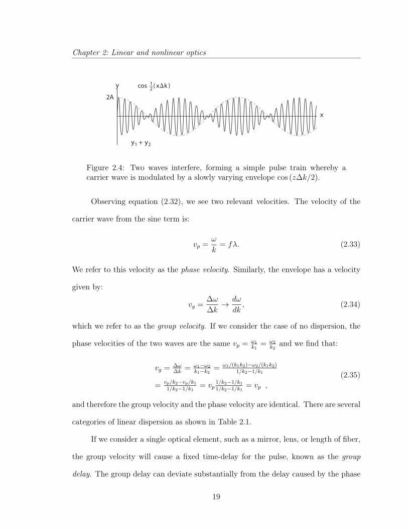
This expression takes the form of a fast oscillating term (the sine function)
modulated slowly by the cosine function. To visualize this behavior, we set t = 0 and
plot equation (2.32) in Figure 2.4. We see the beating between these two frequencies
forms the basis of a simple pulse or group. We call the cosine function the envelope,
and the fast oscillatory part the carrier.
18
Chapter 2: Linear and nonlinear optics
x
y
2A
y1 + y2
12 s o c ( x k )
Figure 2.4: Two waves interfere, forming a simple pulse train whereby acarrier wave is modulated by a slowly varying envelope cos (z∆k/2).
Observing equation (2.32), we see two relevant velocities. The velocity of the
carrier wave from the sine term is:
vp =ω
k= fλ. (2.33)
We refer to this velocity as the phase velocity. Similarly, the envelope has a velocity
given by:
vg =∆ω
∆k→ dω
dk, (2.34)
which we refer to as the group velocity. If we consider the case of no dispersion, the
phase velocities of the two waves are the same vp = ω1
k1= ω2
k2and we find that:
vg = ∆ω∆k
= ω1−ω2
k1−k2= ω1/(k1k2)−ω2/(k1k2)
1/k2−1/k1
= vp/k2−vp/k1
1/k2−1/k1= vp
1/k2−1/k1
1/k2−1/k1= vp ,
(2.35)
and therefore the group velocity and the phase velocity are identical. There are several
categories of linear dispersion as shown in Table 2.1.
If we consider a single optical element, such as a mirror, lens, or length of fiber,
the group velocity will cause a fixed time-delay for the pulse, known as the group
delay. The group delay can deviate substantially from the delay caused by the phase
19

Chapter 2: Linear and nonlinear optics
Table 2.1: Types of linear dispersion
dndω> 0 normal dispersion vg < vp
dndω
= 0 no dispersion vg = vp
dndω< 0 anomalous dispersion vg > vp
velocity (inversely dependent on the index) in a dispersive media. The difference
between the phase and group velocity within a single optical element will cause an
offset between the absolute phase of the carrier and the envelope of the pulse, known
as the carrier-envelope offset.
Gaussian pulse
In our simple model, we have only considered two propagating waves. As we add
more waves in between these initial waves, the envelope is no longer defined by a
simple cosine function and the pulses can separate in time, as shown in Figure 2.3.
To describe such a pulse, we use the slowly-varying envelope approximation (in phasor
notation):
~E (z, t) = A (z, t) ei(kz−ω0t)x. (2.36)
Here, A (z, t) is the envelope function and exp (i (kz − ω0t)) is the carrier. A Gaussian
is a common shape for an ultrashort pulse, given by:
~E (z, t) = ~E0 exp(−1
2
(tτ
)2)ei(kz−ω0t)
= ~E0 exp
(−2 ln (2)
(t
τFWHM
)2)ei(kz−ω0t),
(2.37)
Here, ~E0 is the amplitude of the electric field, t is time and both τ and τFWHM reflect
the pulse duration. Additionally, ω0 and k are the angular frequency and wavevector
20

Chapter 2: Linear and nonlinear optics
of the carrier wave (respectively).
We can measure the pulse duration in several ways by applying different clipping
levels (1/e,1/e2, full-width at half maximum) and calculating these in terms of either
the electric field or the power. Using equation (2.37), we define two definitions for
the pulse duration with respect to the time-averaged power:
P (t) = Pp exp(−(t/τ)2) = Pp exp
(−4 ln (2) (t/τFWHM)2) . (2.38)
Here, P (t) is the power as a function of time t, and Pp is the peak power. In the
first pulse-duration definition, τ is the duration from the peak to the 1/e-clipping
level and is often used for its mathematical simplicity. Experimentally, we use the
full-width at half-maximum duration, related to τ using τFWHM = 2√
ln 2τ .
A Gaussian pulse is very convenient because the spectrum also takes the shape
of a Gaussian. A pulse is as short as possible if the spectral phase is frequency-
independent. We refer to such a pulse as being transform limited and we use the time-
bandwidth product: τ∆ν ≈ 0.44 (for a Gaussian). Alternatively, we can write this
expression in terms of wavelength to show: τ ≈ 0.44λ2/(c∆λ). Thus, the transform
limited pulse duration is inversely dependent on the spectral width. For example, a
transform limited 100-fs pulse has a spectral width of ∆λ ≈ 9.4 nm at 800 nm and a
width of ∆λ ≈ 35.3 at 1550 nm.
2.1.4 Temporal pulse broadening
We observed how a frequency-dependent propagation constant gives rise to phase
velocity and group velocity. If we continue to expand the propagation constant in a
21

Chapter 2: Linear and nonlinear optics
Taylor series, we see:
k (ω) = k0 + dkdω
∣∣ω0
(ω − ω0) + 12d2kdω2
∣∣∣ω0
(ω − ω0)2 + . . .
= k0 + k′ (ω − ω0) + 12k′′(ω − ω0)2 + . . . .
(2.39)
Of these coefficients, we recall that k0 and k′ are related to the phase and group
velocities, respectively. We find that higher order dispersion, beginning with k′′,
begins to change the shape of the pulse, reducing the peak intensity, and is therefore
a critical factor for many nonlinear experiments.
Group velocity dispersion
There is a simple way to think about the spreading of a pulse as it propagates in
a material. Consider a transform limited pulse of light, consisting of a spectrum of
colors. If we cut the spectrum in half, we will have a higher-energy “blue” pulse and
a lower-energy “red” pulse. If we propagate these partial pulses in a media with only
linear dispersion (k′ is constant and k′′ = 0), both will propagate with the same group
velocity, and we can recombine the blue and red pulses to obtain the original pulse
duration. If the medium has higher order dispersion, k′′ 6= 0 and the group velocity
changes as a function of frequency, causing the red and blue pulses to separate in time
as they propagate. When we recombine them, there will be a delay between the red
and blue pulses, and their combination will be of longer duration than the original
pulse. This fixed delay is known as the group delay dispersion (GDD). An optical
element, such as a fixed length of fiber or a microscope objective, will have a fixed
amount of GDD.
If we care about the pulse duration as we propagate, we require the GDD per
22
Chapter 2: Linear and nonlinear optics
unit length, which is known as the group velocity dispersion (GVD). We define the
group velocity dispersion in a material as:
GVD =∂
∂ω
(1
vg
)=
∂
∂ω
(∂k
∂ω
)=∂2k
∂ω2, (2.40)
GVD has units of time squared per length (often fs2/mm).
We can clarify the difference between GDD and GVD by considering an exper-
iment that consists of several optics (mirrors, lenses, etc.) leading up to a nonlinear
pulse propagation experiment (for example, a fiber or a photonic chip). Each optical
element before the fiber adds a fixed amount of GDD, broadening the pulse. However,
we must consider the interplay between the nonlinearity and dispersion as the pulse
propagates within the fiber and therefore, we consider the fiber’s GVD.
Just as we have normal and anomalous dispersion previously, the group velocity
dispersion can be normal or anomalous. Here, we consider positive values of the GVD
as normal and negative values as anomalous. This labeling convention is because most
materials at visible wavelengths show normal GVD. For example, the GVD of silica is
normal (positive) in the visible, reaches zero around 1.3 µm, and becomes anomalous
(negative) for longer wavelengths, such as 1.5 µm.
To make things slightly more confusing, the optical engineering community takes
the derivative of the refractive index with respect to the wavelength, producing an-
other term, known as the dispersion parameter D given by:
D = −λc
d2n
dλ2= −2πc
λ2GVD = −2πc
λ2
∂2k
∂ω2. (2.41)
The dispersion parameter has units of time per length squared, often specified in
ps/nm/km. These units are convenient when we estimate strong pulse broadening.
23
Chapter 2: Linear and nonlinear optics
It is important to note that the sign of the dispersion parameter is opposite to that
of GVD, and thus, a material with anomalous dispersion has a positive dispersion
parameter. These are often used interchangeably, so one should avoid saying “positive”
and “negative” dispersion and instead use “normal” and “anomalous” dispersion.
Dispersive pulse broadening
To observe dispersive broadening, we can consider the Gaussian pulse from equa-
tion (2.37) and apply the effects of group velocity dispersion given by k′′. To simplify
the analysis, we assume k0 = 0 and k′ = 0, both of which will not broaden our pulse,
as we have shown. We take the Fourier transform of equation (2.37):
E (z = 0, ω) =1√2π
∫ ∞−∞
E0e−t22τ2 e−iω0teiωtdt = E0τe
−τ2(ω0−ω)2
2 . (2.42)
From here, we can add the spectral phase and take the inverse Fourier transform:
E (z = L, t) = 1√2π
∫∞−∞E0τe
−τ2(ω0−ω)2
2 e−ik′′2
(ω−ω0)2Le−iωtdω
= τE0√τ2+ik′′L
e
−t2
2τ2(
1+( k′′Lτ2 )
2)2
ei k′′Lt2
2((k′′L)2+τ4) e−iω0t.
(2.43)
We notice that the amplitude changes as the pulse broadens and there is additional
phase from the propagation. We also observe that the middle term closely resembles
the form of equation (2.42) if we let:
τ ′ = τ
√1 +
(k′′L
τ 2
)2
, (2.44)
thus, the pulse broadens in time by√
1 + (k′′L/τ 2)2. We can write this expression in
terms of the full-width at half-maximum to show:
τ ′FWHM = τFWHM
√1 +
(4 ln 2
GVD
τFWHM2d
)2
≈ 4 ln 2GVD
τFWHMd, (2.45)
24
Chapter 2: Linear and nonlinear optics
as it propagates through a distance d. This approximation is valid for strong dispersive
broadening. For silica fiber at 800 nm, GVD = 36 fs2/mm, which corresponds to a
dispersion parameter D of −106 ps/nm/km. Consider a 100 fs pulse at 800 nm;
after propagating through 1 m of silica fiber, it will have a duration of 1 ps. As the
broadening is very strong, we see that using the dispersion parameter is convenient
to estimate the pulse duration. For this situation, a 100-fs pulse at 800 nm has a
spectral bandwidth of ∆λ ≈ 9.4 nm, thus ∆τ ≈ |−106 ps/nm/km| (9.4 nm× 1 m) =
996 fs, which is approximately correct. However, this expression is invalid for small
broadening, for example, from a 10-cm length of fiber. Recall that a short pulse has
a wide bandwidth and is therefore more susceptible to dispersive broadening than
a longer pulse with a reduced bandwidth. This phenomenon creates the counter-
intuitive effect where a narrowed spectrum can produce a shorter pulse for a given
amount of dispersion.
Group velocity dispersion compensation
To facilitate strong nonlinear interactions with low pulse energies, we require very
short pulses. As each optical element adds dispersion, potentially broadening the
pulse, we address the practical concern of pulse compression here. As the change in
pulse duration is a linear effect, we can counteract an amount of normal GDD with
an equal amount of anomalous GDD to recover the original pulse duration. With
sufficient GDD, we can pre-compensate additional optics to form the shortest pulse
somewhere later in the optical path. For visible and most NIR optical elements, the
dispersion is normal. To compensate, we can use a device that has tunable anomalous
25

Chapter 2: Linear and nonlinear optics
GDD known as a pulse compressor.
Tunable anomalous group delay dispersion can be achieved using both gratings
and prisms, as shown in Figure 2.5 (top and bottom, respectively). These configura-
tions consist of four elements (gratings or prisms) such that the first two provide half
of the intended group delay dispersion starting with a collimated beam and ending
with parallel, spatially dispersed colors. The second pair provides the second half
of the GDD and reforms the collimated beam. Very often, we use a single grating
or prism pair with a mirror that reflects the spatially dispersed colors backward to
“fold” the compressor onto itself. This folding-mirror is angled slightly so that the
compressed, retroreflected beam can be diverted by another mirror that is initially
missed by the incoming beam
Figure 2.5: Schematic of a two types of pulse compressors: a grating com-pressor (top) and a prism compressor (bottom).
To determine the GDD through a grating or prism pair, we determine the
26
Chapter 2: Linear and nonlinear optics
wavelength-dependent path length and the resulting phase through a single pair.
From here, we calculate d2ϕ/dω2. For the case of a grating pair, the total GDD
is [14]:d2ϕ
dω2= − (1/ω2) (λ/Λ) (2πL/Λ)[
1− (sin θi − λ/Λ)2]3/2 . (2.46)
Here, ω is the angular frequency, λ is the wavelength, Λ is the spatial period, θi is
the angle of incidence of the incoming light, and L is the separation of the gratings.
We tune the amount of dispersion compensation by changing the separation of the
gratings, L.
For the case of a prism pair, the situation is more complicated because of the
additional material dispersion within the prism itself. We find the following approx-
imation is useful for small amount of material dispersion when the prism pair is cut
and aligned to the Brewster angle (for maximum efficiency) [15]:
d2ϕ
dω2≈ λ3
2πc2
[−8L
(dn
dλ
)2
+ 8
(d2n
dλ2
)(D1/e2
)]. (2.47)
Here, L is the separation of the prisms, D1/e2 is the beam diameter (at the 1/e2
clipping level), n is the index of refraction, and c is the speed of light. The first term
provides tunable anomalous dispersion and depends on the prism material and the
separation of the prisms (similar to gratings). The second term is very often normal
and depends on the propagation length in the prism material.
For a fixed separation L, the amount of dispersion compensation obtained using
gratings is very large compared to prisms, making for shorter separation distances
and potentially smaller footprints. For example, to compensate 1000 fs2 around 800
nm, fused silica prisms require a separation of 77 cm and SF10 glass prisms require
21 cm [15]. A grating compressor with 600 grooves/mm and a 13° angle requires
27
Chapter 2: Linear and nonlinear optics
only 2.8 mm of separation to achieve the same dispersion compensation. Although,
gratings compressors can correct for very strong dispersion, they typically have high
amounts of loss and cannot be used for all applications, such as intra-cavity dispersion
compensation for a femtosecond laser.
2.2 Nonlinear optics
The strong electric fields achievable in a laser can drive the motion of electrons and
atoms to create a nonlinear polarization. This nonlinear polarization gives rise to
many effects, from the generation of new frequencies to light-by-light modulation. In
this section, we will explore these effects and establish a foundation to later explore
all-optical devices.
2.2.1 Nonlinear polarization
For weak electric fields, the polarization depends linearly on the material susceptibility
(in SI units):
~P = ε0χ~E. (2.48)
For stronger electric fields, we expand equation (2.48):
P = ε0
(χ(1)E + χ(2)E2 + χ(3)E3 + ...
), (2.49)
to produce a series of polarizations:
P = P (1) + P (2) + P (3) + ..., (2.50)
where P (1) ≡ ε0χ(1)E is the linear polarization, P (2) = ε0χ
(2)E2 is the second-order
nonlinear polarization, and so on. Although we have written this polarization in
28

Chapter 2: Linear and nonlinear optics
terms of scalars, the electric field is a vector quantity and therefore χ(1) is a second
rank tensor (with 9 elements), χ(2) is a third rank tensor (27 elements), and χ(3) is
a fourth rank tensor (81 elements), to which we often apply symmetry arguments to
isolate unique, non-zero terms [16].
These nonlinear polarization terms act as a driving field in the wave equation,
forming the nonlinear wave equation:
∇2 ~E − n2
c2
∂2 ~E
∂t2=
1
ε0c2
∂2 ~PNL
∂t2. (2.51)
Here, n is the linear index of refraction and PNL is the nonlinear polarization (ex-
cluding the linear term from equation (2.50) contained within n). This driving term
acts as a source of new propagating waves.
Second-order nonlinear polarization
The second order nonlinear polarization is responsible for several effects involving
three photons. For example, two photons can combine to make a third photon. If the
two initial photons are of the same (different) frequency, this effect is second harmonic
generation (sum-frequency generation). Alternatively, one photon can split to make
two photons through difference frequency generation.
Not all bulk crystals exhibit second-order nonlinearities. Let us consider the
centrosymmetric case where a crystal has inversion symmetry. For the second order
polarization, we find that:
~P (2) = ε0χ(2) ~E ~E. (2.52)
If we invert the sign of the fields, we expect the same polarization, only with an
29
Chapter 2: Linear and nonlinear optics
opposite sign, therefore:
− ~P (2) = ε0χ(2)(− ~E)(− ~E)
= ε0χ(2) ~E ~E. (2.53)
Both equations cannot be simultaneously true in a centrosymmetric material unless
χ(2) vanishes. Therefore, materials possessing inversion symmetry do not exhibit
second-order nonlinearities within the bulk material. Only a handful of materials,
typically crystals, are non-centrosymmetric and exhibit χ(2) nonlinearities. Mean-
while, most materials have inversion symmetry including many crystals such as TiO2,
amorphous materials such as glasses, as well as liquids and gases. However, inversion
symmetry is broken at an interface, leading to second-order nonlinearities even for
materials with bulk inversion symmetry [17,18].
Now, let us consider second-harmonic generation in a non-centrosymmetric crys-
tal. Here, we have an electric field given by:
~E (~r, t) =1
2
(E (~r, t) e−iω0t + c.c.,
)x, (2.54)
where we consider a single polarization in the x-direction. We use the slowly varying
envelope approximation through the use of the scalar field E (~r, t), which we will refer
to simply as E. The nonlinear polarization is given by:
~PNL (~r, t) =1
2
(PNL (~r, t) e−iωNLt + c.c.
)x, (2.55)
which produces a second-order polarization:
~P (2) = ε0χ(2) ~E ~E = ε0χ
(2)
[EE∗
2+
1
2
(E2
2e−i2ω0t + c.c.
)]xx. (2.56)
From this expression, we see two terms. The first is at zero frequency, and is not
responsible for generating a propagating wave as it vanishes when operated on by the
30
Chapter 2: Linear and nonlinear optics
time-derivative in the wave equation. The next term is at twice the initial frequency,
known as the second harmonic. We can solve this expression for the slowly varying
amplitude of the nonlinear polarization and the frequency to show:
P(2)2ω0
= ε0χ(2)E2
2and ωNL = 2ω0. (2.57)
The process of generating second-harmonic signal efficiently requires additional con-
siderations, known as phase matching, which is often achieved using birefringent
crystals [19]. In a similar way, a field consisting of two different frequencies can gen-
erate terms at the second harmonic of each frequency, as well as for their summation
and difference.
Third-order nonlinear polarization
The majority of materials are centrosymmetric and therefore, the first non-zero non-
linear polarization is usually the third-order polarization. Writing this polarization
out, we find:
~P (3) (t) = ε0χ(3) ~E ~E ~E = ε0χ
(3)
[1
2
(E3
4e−i3ω0t + c.c.
)+
1
2
(3
4|E|2Ee−iω0t + c.c.
)]xxx.
(2.58)
Two terms emerge, leading to distinct physical processes. As before, the slowly
varying envelope amplitude and nonlinear frequency for the first term is:
P(3)3ω0
= ε0χ(3)E3
4and ωNL = 3ω0, (2.59)
respectively. This term is responsible for third harmonic generation. This process is
often not efficient unless we use phase-matching techniques.
31
Chapter 2: Linear and nonlinear optics
Meanwhile, the second term is extremely relevant, as the polarization occurs at
the original frequency. The slowly varying amplitude and nonlinear frequency are:
P(3)ω0 = 3ε0χ(3)|E|2E
4and ωNL = ω0. (2.60)
This effect leads to a nonlinear index of refraction and is extremely important for
devices. The nonlinear index is perhaps the most frequently observed nonlinearity.
Not only do all materials exhibit third-order nonlinearities, but also, phase-matching
is automatically satisfied as the polarization is at the original frequency. Therefore,
we can observe this nonlinear effect without the specialized configurations required
of other nonlinearities, such as second- and third-harmonic generation.
Anharmonic oscillator model
In the same way that we used the Drude-Lorentz model to gain physical insight into
the linear dielectric function, we can use the classical anharmonic oscillator model to
explore electronic nonlinearities. We base this nonlinear model on the same principles
as before, but replace the binding force with an altered, nonlinear force. Just as the
binding force for the Drude model is proportional to an electron’s displacement from
its equilibrium position (x), the second-order polarization requires a term proportional
to x2. For the (more applicable) third-order case, the binding force is:
Fbinding = −mω02x+mbx3, (2.61)
where we have introduced a force term proportional to x3 with a phenomenological
proportionality constant of b. Typically, b is on the order of ω20/d
2, where d is on the
32
Chapter 2: Linear and nonlinear optics
order of the Bohr radius [16]. The equation of motion becomes:
md2x
dt2+mγ
dx
dt+mω0
2x−mbx3 = −eE0e−iωt. (2.62)
We proceed in much the same way as before, which we will not show here. For the
case of self-phase modulation, we arrive at [16]:
χ(3) =Nbe4
ε0m3D(ω)3D (−ω), (2.63)
where D (ω) = ω20 − ω2 − iγω. This expression takes a very similar form as χe from
equation (2.18), with additional factors of e2 andm−2, along with multiple degenerate
resonances given by D(ω). We can approximate this expression if we are far from
resonance using:
χ(3) ≈ Ne4
ε0m3ω60d
2. (2.64)
2.2.2 Nonlinear index of refraction
The third-order nonlinear polarization gives rise to a nonlinear index of refraction that
we use to make all-optical devices. An intensity-dependent index leads to self-phase
modulation (SPM) for coherent waves and cross-phase modulation for non-coherent
waves. In addition, by allowing χ(3) to take on complex values, we discover a new
source of nonlinear absorption, analogous to the linear absorption caused by a complex
χ(1).
33

Chapter 2: Linear and nonlinear optics
Intensity-dependent refractive index
If we take the slowly varying envelope amplitudes for the linear polarization P (1) =
ε0χ(1)E and add this new term, we can write an effective linear susceptibility:
P (1) + P (3)ω0
= ε0χ(1)E +
3ε0χ(3)|E|2
4E = ε0
(χ(1) +
3χ(3)
4|E|2
)E = ε0χ
(1)effE. (2.65)
This effective susceptibility creates an effective index of refraction:
n =√
Re (ε) =
√Re(
1 + χ(1)eff
)=
√1 + Re (χ(1)) +
3Re (χ(3))
4|E|2, (2.66)
which we can simplify by expanding around small |E|2:
n ≈√
1 + Re (χ(1)) +3Re
(χ(3))
8√
1 + Re (χ(1))|E|2 = n+
3
8nRe(χ(3))|E|2 = n+ n2|E|2.
(2.67)
This derivation produces our first definition of the nonlinear refractive index (in terms
of |E|2):
n2 =3
8n0
Re(χ(3)). (2.68)
In terms of the intensity, equation (2.67) becomes:
n = n0 + n2I = n0 +3
4n20ε0c
Re[χ(3)]I. (2.69)
The nonlinear index is often referred to as the Kerr effect. For a single wave
propagating in a Kerr-medium, the wave’s intensity modulates the index of refraction,
which modulates the phase of the wave as it propagates. We refer to this process as
self-phase modulation. A similar effect occurs across different, non-coherent waves,
known as cross-phase modulation [16]. We note that n2 can be either positive or neg-
ative, depending on the origin of the nonlinearity (electronic polarization, molecular
34
Chapter 2: Linear and nonlinear optics
orientation, thermal, etc.). For the electronic, non-resonant nonlinear polarization in
silica, n2 is positive and therefore, we will assume a positive value of n2. For silica,
the nonlinear index of refraction is 2.2–3.4 ×10⁻²⁰ m2/W [20,21].
We have used SI units during this derivation, thus χ(3) is in units of m2/V2.
Often χ(3) is given in electrostatic units (cm3/erg, or simply esu). Meanwhile, the
nonlinear index is typically quoted in units of cm2/W. The conversion is [16]:
n2
(cm2
W
)=
12π2
n20c
107χ(3)esu. (2.70)
Two-photon absorption
Using a complex valued χ(3), we see that the third-order nonlinear polarization implies
a nonlinear extinction coefficient, given by:
κ = κ0 + κ2I = κ0 +3
4n20ε0c
Im[χ(3)]I. (2.71)
Using α = 2ω0κ/c, we can write this expression as the nonlinear absorption:
α (I) = α0 + α2I = κ0 +3ω0
2n20ε0c2
Im[χ(3)]I. (2.72)
The new term is responsible for two-photon absorption and has units of length per
power. For two-photon absorption to occur, the total energy of both photons must
be large enough to promote an electron from the valence to the conduction band,
and therefore χ(3) must necessarily be frequency dependent. For degenerate (same
frequency) two-photon absorption, the single-photon energy must be at least half of
the band-gap energy.
We note that two-photon absorption is a third-order process and not a second-
order process. We can see this distinction by observing equation (2.58), whereby
35
Chapter 2: Linear and nonlinear optics
the imaginary third-order nonlinear polarization produces a wave at the original fre-
quency. This out-of-phase wave adds destructively with the original wave, resulting
in attenuation.
Nonlinear index scaling
Understanding how n2 scales with bandgap energy helps us select candidate materi-
als for all-optical applications. To understand how n2 scales, we consider a direct-
bandgap semiconductor with bandgap energy of Eg and photon energies less than Eg.
Sheik-Bahae et al. developed a simple model for an instantaneous nonlinearity which
neglects one-photon processes to describe the scaling of two-photon absorption and
the nonlinear index [10, 22]. We find that, under these approximations, two-photon
absorption has the form:
α2 =K√Ep
n20E
3g
F2 (2~ω/Eg) , (2.73)
where K is an empirical constant found to be 3.1 × 10³ when Ep and Eg are in eV
and n2 is in units of cm2/W, and Ep = 21 eV. Here, we use the universal function:
F2 (2x) = (2x−1)3/2
(2x)5 for 2x > 1. (2.74)
We can related this expression to n2 using a nonlinear version of the Kramers-Kronig
relation to show:
n2 = K~c√Ep
2n20E
4g
G2 (~ω/Eg) , (2.75)
where:
G2 (x) =−2 + 6x− 3x2 − x3 − 3
4x4 − 3
4x5 + 2(1− 2x)3/2Θ (1− 2x)
64x6, (2.76)
36
Chapter 2: Linear and nonlinear optics
with Θ(y) being the Heaviside step function.
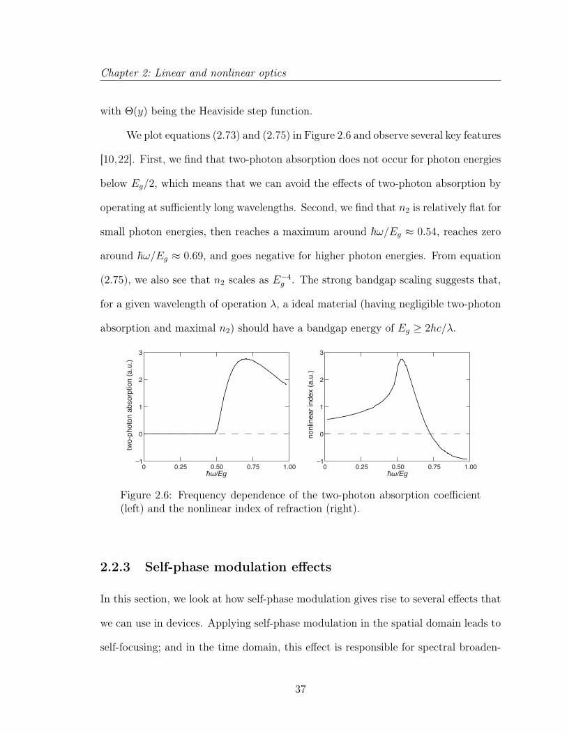
We plot equations (2.73) and (2.75) in Figure 2.6 and observe several key features
[10,22]. First, we find that two-photon absorption does not occur for photon energies
below Eg/2, which means that we can avoid the effects of two-photon absorption by
operating at sufficiently long wavelengths. Second, we find that n2 is relatively flat for
small photon energies, then reaches a maximum around ~ω/Eg ≈ 0.54, reaches zero
around ~ω/Eg ≈ 0.69, and goes negative for higher photon energies. From equation
(2.75), we also see that n2 scales as E−4g . The strong bandgap scaling suggests that,
for a given wavelength of operation λ, a ideal material (having negligible two-photon
absorption and maximal n2) should have a bandgap energy of Eg ≥ 2hc/λ.
ħω/Eg
two-
phot
on a
bsor
ptio
n (a
.u.)
0 0.25 0.50 0.75 1.00
3
2
1
0
–1
ħω/Eg
nonl
inea
r in
dex
(a.u
.)
0 0.25 0.50 0.75 1.00
3
2
1
0
–1
Figure 2.6: Frequency dependence of the two-photon absorption coefficient(left) and the nonlinear index of refraction (right).
2.2.3 Self-phase modulation effects
In this section, we look at how self-phase modulation gives rise to several effects that
we can use in devices. Applying self-phase modulation in the spatial domain leads to
self-focusing; and in the time domain, this effect is responsible for spectral broaden-
37

Chapter 2: Linear and nonlinear optics
ing, supercontinuum generation, and four-wave mixing. These processes require high
intensities to be efficient; therefore, all sources of loss are important for materials
and devices. With losses in mind, we explore the nonlinear figures of merit to assess
current and future materials for third-order nonlinear optical applications.
Nonlinear phase
Understanding the accumulation of nonlinear phase is essential, as it forms the basis
for many all-optical devices. Starting with equation (2.3), we realize that as the wave
propagates, it accumulates a phase given by ϕ = kL, where L is the distance traveled.
Adding the nonlinear index we see:
ϕ = k (I)L =2π
λ(n+ n2I)L =
2πnL
λ+
2πn2L
λI = ϕL + ϕNL. (2.77)
The intensity alters the phase accumulated by a factor of:
φNL =2πn2L
λI, (2.78)
through a process known as self-phase modulation (SPM). For a plane wave at a single
frequency, the wave gains a fixed phase change per unit distance. As we will show in
Appendix C, we can use this nonlinear phase to modulate nonlinear interferometers.
Self-focusing
If we make the intensity non-uniform in space or in time, these gradients results
in self-focusing or spectral-broadening, respectively. To demonstrate the effects of
a spatial non-uniformity, let us consider a Gaussian beam profile passing through a
thin, flat, nonlinear-material. At the center of the beam, the intensity is higher than
38
Chapter 2: Linear and nonlinear optics
at the edges, therefore the center accumulates a larger amount of nonlinear phase. For
a material with a positive nonlinear index, the distribution of nonlinear phase shifts is
analogous to a positive lens and causes the wave to focus. The Z -scan technique uses
this intensity-dependent lens to measure the nonlinearity of bulk samples [23,24].
Spectral broadening
If we make the intensity non-uniform in time using a pulse, self-phase modulation
broadens the pulse’s spectrum. Consider a pulse at a fixed location in space that
has an intensity that changes in time, I(t). Using equation (2.77), we can take a
derivative with respect to time, to find a change in frequency given by:
∆ω = −dϕdt
= −2π
λLn2
dI (t)
dt. (2.79)
For the case of a Gaussian pulse, we remember that equation (2.38) can be
converted to intensity by dividing by an area and replacing Pp → I0. With equa-
tion (2.79), we find the frequency shift for a Gaussian pulse is:
∆ω =2π
λLn2
8 ln (2)
τ 2tI (t) . (2.80)
From this equation, we realize that I(t) is always positive and tI(t) goes from negative
to positive. At a fixed position, negative time is the front of the pulse and therefore,
the front of the pulse experiences a negative frequency shift, creating longer, “red”
wavelengths in the front. Oppositely, the back end of the pulse (positive time values)
is frequency shifted positively and the wavelengths appear “blue-shifted”. These are
new frequencies that are not present in the original pulse. Alternatively, one can
picture this process as the peak of a pulse traveling with a slower phase velocity and
39

Chapter 2: Linear and nonlinear optics
therefore, the carrier wave “stretches out” in the front and “bunches up” in the back,
creating red and blue wavelengths in the front and back, respectively.
Group velocity dispersive effects are extremely important in a real system. For
a positive nonlinearity and normal GVD, both effects cause a “red” wave-packet to
move toward the front of the pulse and a “blue” wave-packet to the back, reducing
the intensity, leading to a limited amount of spectral broadening. If GVD is low,
the broadening can be very strong, forming a continuum of wavelengths, known as
supercontinuum or “white light” generation. In the case of anomalous GVD, the
effects of self-phase modulation and GVD are opposite and can lead to a situation
where the two effects balance one another, creating stable packets of light, known as
solitons.
Nonlinear figures of merit
Material losses limit the performance of SPM-based all-optical switches. Switches
made using nonlinear interferometers, for example, require a specified total nonlinear
phase for full modulation [25–27]. Total losses (both intrinsic and from fabrication)
limit the maximum amount of nonlinear phase by attenuating the wave as it propa-
gates, making full modulation impossible for certain materials [25]. We quantify these
limitations using dimensionless parameters known as the nonlinear figures of merit.
To proceed, we ask: for a given material, what is the maximum amount of
nonlinear phase that the wave can accumulate? Let us consider the simplest case of a
monochromatic plane-wave experiencing both linear and nonlinear attenuation. Our
40

Chapter 2: Linear and nonlinear optics
first step must be to determine the intensity as a function of distance using:
dI (z)
dz= − [α0 + α2I (z)] I (z) . (2.81)
This differential equation has a solution of the form:
I (z) = I0e−α0z
[1 + I0α2
(1− e−α0z
α0
)]−1
. (2.82)
The total nonlinear phase accumulated over a distance L is therefore:
total ϕNL =
∫ L
0
2πn2
λI (z) dz = 2π
(n2
α2λ
)ln
[1 + I0α2
(1− e−α0L
α0
)]. (2.83)
From this expression, we define the effective length for plane-waves and in waveguides
as [24]:
Leff =1− e−α0L
α0
. (2.84)
Taking L→∞, the effective length becomes 1/α0 and the maximum nonlinear phase
is given by:
max ϕNL = 2π
(n2
α2λ
)ln
[1 +
(n2
α2λ
)−1(n2I0
α0λ
)]. (2.85)
From this result, we can define two figures [6, 27]:
W ≡(n2I0α0λ
)and T−1 ≡
(n2
α2λ
), (2.86)
and we can rewrite equation (2.85) as:
max ϕNL = 2πT−1 ln [1 + TW ] . (2.87)
The W and T−1 figures of merit are associated with linear losses and two-photon
absorption, respectively.
41

Chapter 2: Linear and nonlinear optics
Now, let us look at the simplest case, where we have only linear losses, by taking
the limit of equation (2.87) as T−1 → ∞. The maximum nonlinear phase amounts
to 2πW , and if we require max ϕNL > 2π, we require that W > 1. This result sug-
gests the need for a minimum operating intensity: for a given attenuation coefficient
α0 we require an intensity of I0 > α0λ/n2. The damage threshold of the material
or additional nonlinear effects (particularly two- and three-photon absorption) pose
limits for all-optical switching. Alternatively, for a given operating intensity, we must
achieve total losses (absorption and scattering) of α0 < n2I0/λ.
Usually, we are only interested in materials with no intrinsic linear absorption
and therefore, two-photon absorption and imperfections from the fabrication are lim-
iting factors. For strong two-photon absorption, T−1 is small, and the wave is strongly
absorbed at the start of propagation. After the intensity quickly drops, we will con-
tinue to accumulate nonlinear phase at a reduced rate, requiring very large devices
for full modulation. For a fixed value of T−1, we can determine the required value of
max ϕNL > 2π:
Wreq >
(eT − 1
)T
= 1 +1
2T +
1
6T 2 + .... (2.88)
For reasonable values of Wreq (near unity), we use the following guidelines [6, 27]:
W =(n2I0α0λ
)> 1 and T−1 =
(n2
α2λ
)> 1. (2.89)
These two figures of merit are a simple and effective way to evaluate a nonlin-
ear material. Although the intrinsic nonlinearity of silica fiber is relatively low, it
is a fantastic nonlinear material, having exceptionally low loss and low two-photon
absorption. These factors become much more critical in new materials systems with
high nonlinearity and serve as a check for applications. For example, silicon has a
42

Chapter 2: Linear and nonlinear optics
very strong intrinsic nonlinearity, 200–300 times silica glass [7]. However, this high
nonlinearity is accompanied by strong two-photon absorption, and thus the T−1 figure
of merit is below unity for all telecommunications wavelengths and is only above unity
for wavelengths longer than 1800 nm [7]. Although low figures of merit make ultrafast
interferometric switches impractical in silicon, other effects are used for switching [28].
2.3 Nonlinear optics at the nanoscale
In this section, we will explore sub-wavelength waveguides both theoretically and
experimentally and use these later to enhance nonlinear interactions. To motivate
the use of waveguides for nonlinear optics, we observe that the total accumulated
nonlinear phase depends on the intensity and the effective length in equation (2.83).
We can reach high intensities by focusing a laser using a lens; however, the beam will
quickly diverge, leading to few accumulated nonlinearities. Considering a Gaussian
beam, the peak intensity is I0 = 2P0/ (πw20), where P0 is the power, and w0 is the
beam waist. For a focused beam, the divergence limits the length of nonlinear phase
accumulation. If the effective length for a Gaussian beam is given by the Rayleigh
distance zR = πw20/λ, the intensity-length product for a focused beam is [20]:
I0zR =
(2P0
πw20
)(πw2
0
λ
)=
2P0
λ. (2.90)
The intensity is inversely proportional to the square of the spot size, w0; meanwhile,
the focused spot will diverge based on the Rayleigh distance, which is directly pro-
portional to the square of the spot size. These combined effects lead to a situation
whereby tight focusing, alone, does not change the accumulated nonlinearity. We can
43

Chapter 2: Linear and nonlinear optics
achieve much stronger nonlinear interactions if we can counteract the divergence by
keeping the wave confined as it propagates. Such confinement is precisely what we
achieve using a waveguide. If the waveguide has a loss of α0, using equation (2.84),
the intensity-length product is [20]:
I0Leff =
(2P0
πw20
)(1− e−α0L
α0
)≈ 2P0
πw20α0
. (2.91)
The maximum intensity-length product (for a waveguide of infinite length) depends
completely on the loss of the waveguide and is far greater than for a focused beam.
This ability to accumulate a large amount of nonlinear phase in a waveguide is an
essential tool for nonlinear optics. In addition, we see that the nonlinear interaction
scales inversely with the area. Therefore, the highest nonlinear interactions will occur
for waveguides with the smallest effective area and thus, by employing nano-scale
waveguides, we can achieve very large nonlinear interactions efficiently.
2.3.1 Waveguides
Waveguides use multiple reflections to confine light signals into discrete channels,
known as modes. By considering geometrical arguments, we will first develop an
intuitive understanding of the guiding condition using reflections from metallic mir-
rors. Similarly, we will use total internal reflection to form waveguides in dielectric
materials. By observing the wavelength-dependence of the guiding condition, we will
demonstrate how waveguides can alter the effective propagation constant and use
it to engineer the effective dispersion within a waveguide. Lastly, we will observe
the field distributions within waveguides, which will enable us to create enhanced
nonlinearities using sub-wavelength structure.
44

Chapter 2: Linear and nonlinear optics
Metal mirror waveguide
We will start by considering the simplest waveguide formed by two parallel metallic
mirrors. Considering the geometry of Figure 2.7 (left), we see that for the wave to
sustain itself, the phase accumulated from multiple bounces must add constructively
with the original wave. Each bounce off a metal mirror adds a phase shift of π.
Therefore, the total phase from the path length and from each bounce, must be an
integer multiple of 2π. From the geometry in Figure 2.7, this condition is [29]:
2πλ0
(AC − AB)− 2π = 2πλ0
(AC − AC cos (2θ))− 2π
= 2πλ0
2d sin θ − 2π = 2πm′,
(2.92)
where m′ is an integer (starting from zero). Simplifying this expression and using
m = m′ + 1, we obtain:
2d sin θ = mλ0 m = 1, 2, .... (2.93)
Therefore, we have a discrete number of propagating solutions, as shown in Figure 2.7
(right). Each solution is known as a mode and acts like a channel for an electromag-
netic wave. The number of guided modes for a single polarization is given by:
M =·2d
λ0
. (2.94)
We find that no guiding can occur when the distance becomes less than half of the
wavelength.
Depending on the orientation of the electric field, two unique waves can propa-
gate. If the electric field of the wave is transverse to the plane of the mirror, we find the
transverse-electric polarization (TE) and there is no electric field in the direction of
45
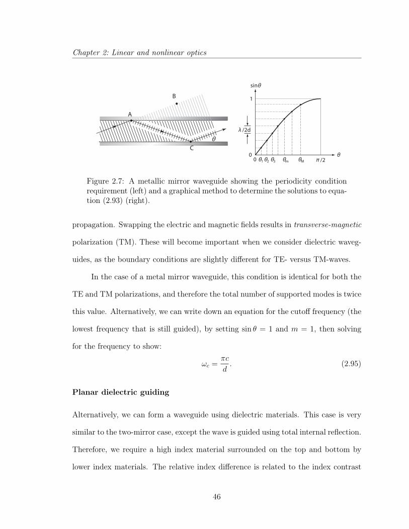
Chapter 2: Linear and nonlinear optics
θ
A
C
B
d
00
1
sinθ
θπ /2
/2dλ
θ mθ 1 θ 2 θ 3 θ M
Figure 2.7: A metallic mirror waveguide showing the periodicity conditionrequirement (left) and a graphical method to determine the solutions to equa-tion (2.93) (right).
propagation. Swapping the electric and magnetic fields results in transverse-magnetic
polarization (TM). These will become important when we consider dielectric waveg-
uides, as the boundary conditions are slightly different for TE- versus TM-waves.
In the case of a metal mirror waveguide, this condition is identical for both the
TE and TM polarizations, and therefore the total number of supported modes is twice
this value. Alternatively, we can write down an equation for the cutoff frequency (the
lowest frequency that is still guided), by setting sin θ = 1 and m = 1, then solving
for the frequency to show:
ωc =πc
d. (2.95)
Planar dielectric guiding
Alternatively, we can form a waveguide using dielectric materials. This case is very
similar to the two-mirror case, except the wave is guided using total internal reflection.
Therefore, we require a high index material surrounded on the top and bottom by
lower index materials. The relative index difference is related to the index contrast
46

Chapter 2: Linear and nonlinear optics
and determines parameters including the number of modes, the phase and group
velocities, GVD and the confinement.
For total internal reflection, the angle between the wavevector and the normal
to the interface must be greater than the critical angle. The critical angle is given by
sin θc = n2/n1, where n1 is the index in the guiding layer and n2 is the cladding index.
We should note that our current waveguide discussion uses the complimentary angle.
In our present notation, waves will be totally internally reflected if θ < (π/2− θc).
Using these conditions, we modify equation (2.92) by scaling the length by the index
of the guiding layer, n1, and we replace the phase-shift upon reflection, previously π,
with a new material- and polarization-dependent phase-shift, ϕ:
2π
λ0
n1 (2d sin θ)− 2ϕ = 2πm′. (2.96)
If we use the convention that λ = λ0/n1, the condition becomes [29]:
2π
λ2d sin θ − 2ϕ = 2πm. (2.97)
The phase change depends on the materials (through θc) and on the polarization
[30]:
ϕTE = 2tan−1
(√cos2θcsin2θ
− 1
), and (2.98)
ϕTM = 2tan−1
(csc2θc
√cos2θcsin2θ
− 1
), (2.99)
for TE- and TM-polarizations, respectively. Using these expressions, we determine
the guiding condition to be:
tan[πdλ
sin θTE − mπ2
]=√
sin2(π/2−θc)sin2θTE
− 1, and (2.100)
47

Chapter 2: Linear and nonlinear optics
sinθ
m = 0 1 2 3 4 5 6 7
LHS
00 sin
/(2d)λ
RHS
sin( /2– c)θπ
Figure 2.8: Graphical solutions to the waveguiding condition from equa-tion (2.101).
tan
[πd
λsin θTM −
mπ
2
]= csc2θc
√sin2 (π/2− θc)
sin2θTM− 1. (2.101)
To find the modes graphically, we can plot both the left- and right-hand sides in terms
of sin θ, the solutions occur whenever the two curves intersect, as shown in Figure 2.8.
In addition, we can calculate the number of modes by determining the number
of crossings. We realize that the left-hand side is periodic in sin θ and we can expect
a solution for each period until the right hand side goes to zero. Considering both
even and odd values of m, the function has a periodicity of λ/ (2d) in terms of sin θ.
We find that the right-hand side goes to zero when sin θ = sin (π/2− θc). Therefore,
the number of modes, M , for TE-polarization is given by:
M=sin (π/2− θc)
λ/ (2d). (2.102)
Note that we must round up in this case. Alternatively, we can write this expression
in terms of the refractive indices use by using:
sin (π/2− θc) = cos θc =√
1− sin2θc =√
1− n22/n
21 =
√n2
1 − n22
n1
, (2.103)
48
Chapter 2: Linear and nonlinear optics
to show:
M=2d
λn1
√n2
1 − n22 =
2d
λ0
√n2
1 − n22, (2.104)
for TE-polarization [29]. (Note the substitution of the free-space wavelength.) This
expression is not correct if we consider an asymmetric waveguide with a different
upper and lower cladding. Similarly, we have a cutoff frequency of [29]:
ωc =πc
d
1√n2
1 − n22
, (2.105)
above which multiple modes of one polarization will propagate.
Multiple modes in a waveguide can make designing and fabricating devices dif-
ficult. Although modes are linearly independent, small perturbations in real systems
can couple multiple modes to one another. Therefore, we often try to make waveguides
single-mode. We consider a waveguide single-mode if it only supports a single guided
mode for a particular polarization (TE or TM). We can obtain single-mode operation
by adjusting the waveguide materials and geometry, as shown in equations (2.94) and
(2.104).
Comparing the single-mode condition for mirror versus dielectric guiding, we
find that using 600-nm light, the single-mode thickness d for mirror guiding is in the
range from 300–600 nm, below which, no modes are supported. On the other hand,
for fused silica, we find single-mode guiding for thicknesses less than 283 nm, with
no minimum thickness, in contrast to the mirror guided case. If we reduce the index
contrast between the core and the cladding, we can increase the size of the waveguide,
as is done for standard silica fiber.
49
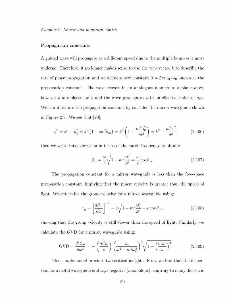
Chapter 2: Linear and nonlinear optics
Propagation constants
A guided wave will propagate at a different speed due to the multiple bounces it must
undergo. Therefore, it no longer makes sense to use the wavevector k to describe the
rate of phase propagation and we define a new constant β = 2πneff/λ0 known as the
propagation constant. The wave travels in an analogous manner to a plane wave,
however k is replaced by β and the wave propagates with an effective index of neff .
We can illustrate the propagation constant by consider the mirror waveguide shown
in Figure 2.9. We see that [29]:
β2 = k2 − k2y = k2
(1− sin2θm
)= k2
(1− m2λ2
0
4d2
)= k2 − m2π2
d2, (2.106)
then we write this expression in terms of the cutoff frequency to obtain:
βm =ω
c
√1−m2
ω2c
ω2=ω
ccos θm. (2.107)
The propagation constant for a mirror waveguide is less than the free-space
propagation constant, implying that the phase velocity is greater than the speed of
light. We determine the group velocity for a mirror waveguide using:
vg =
[dβmdω
]−1
= c
√1−m2
ω2c
ω2= c cos θm, (2.108)
showing that the group velocity is still slower than the speed of light. Similarly, we
calculate the GVD for a mirror waveguide using:
GVD =d2βmdω2
= −(m2ω
c
)(ωc
ω2 −m2ω2c
)2√
1−(mωc
ω
)2
. (2.109)
This simple model provides two critical insights. First, we find that the disper-
sion for a metal waveguide is always negative (anomalous), contrary to many dielectric
50
Chapter 2: Linear and nonlinear optics
ky
z
kβm
Figure 2.9: Propagation constant for a metallic mirror waveguide.
materials. Secondly, we find that the GVD depends heavily on the cutoff frequency
of the waveguide ωc = πc/d and becomes very strong as we approach the cutoff fre-
quency. Therefore, the GVD is heavily dependent on the waveguide geometry. Thus,
by changing the mirror separation d, we have the ability to tune the GVD, which we
have seen is a critical parameter for pulse propagation.
In a similar way, we determine the propagation constant for a dielectric waveg-
uide starting with:
2d
√ω2
c21
− β2 = 2ϕr + 2πm, (2.110)
with integer values of m. Similar to the mirror waveguide, we can use this condition
to derive the group velocity for a dielectric waveguide. The derivation is rather
mathematical and is of limited use in the present context. Therefore, we refer the
51
Chapter 2: Linear and nonlinear optics
reader to the derivation presented in [29], and present the result here:
vg =d cot θ + ∆z
n1d csc θ/c+ ∆τ. (2.111)
Here, n1 is the refractive index of the core, θ is the angle associated with the
planar mode. In addition, we have introduced ∆z, which corresponds to the additional
distance that the wave propagates along the boundary in the form of an evanescent
wave for each round trip. This additional propagation takes a time ∆τ . We can
relate this result to our previous result, if we have no evanescent field by setting
∆z = ∆τ = 0. Equation (2.111) reduces to equation vg = (c/n1) cos θ, which is
identical to (2.108), with the addition of a dielectric between the two mirrors.
Just as for a metal mirror waveguide, the group velocity depends on the thickness
of the dielectric waveguide. The dielectric’s intrinsic GVD alters the total GVD, which
is sometimes approximated as the sum of the material dispersion and the waveguide
dispersion [31, 32]. We must also consider the penetration of the evanescent wave
into the cladding. Because of these considerations, and the complications of a two-
dimensional waveguide cross-section, we often use numerical simulations.
As many materials display normal GVD at optical frequencies, we are often
interested in reducing the amount of normal dispersion by introducing anomalous
waveguide dispersion. For this case, we see two general design considerations. First,
we should design our waveguides with dimensions that are comparable to the wave-
length of interest (near cutoff). Second, we should use core and cladding materials
with high index-contrasts to reduce the penetration of the evanescent field and better
approximate the strong anomalous dispersion found in the mirror waveguide.
52
Chapter 2: Linear and nonlinear optics
Waveguide equation
Light propagates differently in a waveguide than it does in free-space; however, it
is similar to plane wave propagation. To reflect this similarity, we can rewrite the
wave equation and look for solutions that take the same form as plane waves. We
use a spatially varying dielectric constant εr (x, y) that is infinite in the z-direction.
We start with the equation for the time-harmonic vector and scalar potentials in a
source-free, non-magnetic, non-uniform, dielectric medium [14]:
∇2 ~A+ ω2 εrc2~A = −i ω
c2∇εrΦ. (2.112)
The electric field is determined by ~E = −iω ~A−∇Φ. We see that the right hand side
of equation (2.112) couples the vector and scalar potential. If we assume that ∇εr is
small and set it to zero, we can obtain:
∇2 ~A+ω2
c2εr ~A = 0. (2.113)
We can look for solutions that resemble plane waves of the form:
~A = ~yF (x, y) e−iβz, (2.114)
where we assume that all the of z dependence is in e−iβz, and therefore F (x, y) is the
modal distribution, which describes the spatial profile of the mode. After substitution,
the differential equation for F (x, y) is:
∇2TF +
(−β2 +
ω2
c2εr (x, y)
)F = 0, (2.115)
where ∇2T is the Laplacian in the transverse spatial direction. This equation has
the same form as the time-dependent Schrodinger equation for a two-dimensional
53

Chapter 2: Linear and nonlinear optics
potential well with a potential of −ω2µ0ε (x, y). Therefore, this equation’s solutions
are completely analogous to those for a quantum well and, as we’ve seen previously,
requires specific values of the propagation constant β.
Waveguide field distributions
For the case of a metallic mirror waveguide, the electric field must necessarily be zero
at the metallic boundary. However, for the case of dielectric waveguides, the field ex-
tends beyond the boundary as a decaying evanescent field. Solving equation (2.115),
a TE mode has an internal field given by [29]:
Fm (y) ∝
cos(2π sin θm
λy), m = 0, 2, 4, ...
sin(2π sin θm
λy), m = 1, 3, 5, ...
− d
26 y 6
d
2, (2.116)
with λ = λ0/n1. Outside of the waveguide core, the evanescent field is given by:
Fm (y) ∝
exp[−(n2k0
√cos2θm
cos2(π/2−θc) − 1)y],
exp[(n2k0
√cos2θm
cos2(π/2−θc) − 1)y],
y > d/2
y < −d/2.
(2.117)
We see the evanescent field decays into the surrounding medium, as shown in equa-
tion (2.117). The higher order modes, having larger angles θm, will extend further
into the cladding [29].
Just as for quantum wells, there are analogous oscillatory solutions for waveg-
uides, as shown in Figure 2.10. For mirror waveguides, the modes resemble an infinite
quantum well, with the wave going to zero at the boundaries (Figure 2.10, left). Al-
ternatively, we see that waves guided by a dielectric extend beyond the boundaries
and propagate in the form of an evanescent wave, analogous to a finite quantum well
(Figure 2.10, right).
54
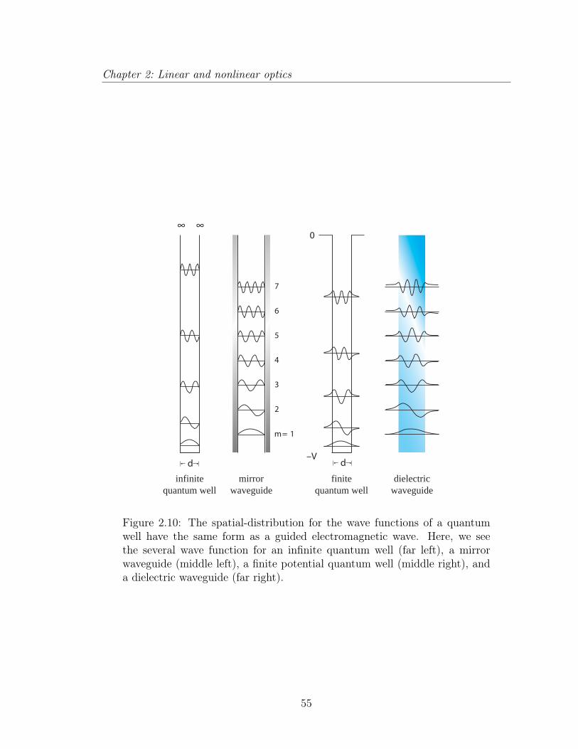
Chapter 2: Linear and nonlinear optics
m= 1
2
3
4
5
6
7
0
–Vd
∞ ∞
d
infinitequantum well
mirrorwaveguide
finitequantum well
dielectricwaveguide
Figure 2.10: The spatial-distribution for the wave functions of a quantumwell have the same form as a guided electromagnetic wave. Here, we seethe several wave function for an infinite quantum well (far left), a mirrorwaveguide (middle left), a finite potential quantum well (middle right), anda dielectric waveguide (far right).
55

Chapter 2: Linear and nonlinear optics
We have only dealt with planar waveguides so far, for simplicity. We can confine
the wave in the other transverse dimension as well, which enables us to concentrate
light strongly in two-dimensions. Adding an additional degree of freedom leads to
many different type of waveguides including cylindrical waveguides, such as fibers, as
well as rectangular waveguides such as channel, strip, and ridge waveguides [13].
2.3.2 Nonlinear pulse propagation
The generalized nonlinear Schroedinger equation (NLSE) is the workhorse of nonlinear
fiber and integrated optics. It adds a third-order nonlinear response to the waveguide
equation and describes the temporal evolution of a pulse in a nonlinear waveguide.
Although we will discuss the simplest version here, we can extend this model to
include wide-bandwidth pulses, a delayed nonlinearity, and two-photon absorption.
Nonlinear Schroedinger equation
To develop the nonlinear Schroedinger equation, we will follow the derivation by
Agrawal [20]. Let us consider the wave equation in terms of the linear and nonlinear
polarization in the time domain:
∇2 ~E − 1
c2
∂2 ~E
∂t2= µ0
∂2 ~PL∂t2
+ µ0∂2 ~PNL∂t2
. (2.118)
Our strategy for simplifying this differential equation starts by including the nonlinear
polarization into an effective dielectric constant εeff (ω). Next, we use separation of
variables to isolate a transverse-wave equation from the propagation equation, as
we did when analyzing the modes in a waveguide. We incorporate the nonlinear
polarization by solving the transverse equation and using the nonlinear part of εeff (ω)
56
Chapter 2: Linear and nonlinear optics
as a perturbation. The lowest order perturbation alters the propagation constant,
while keeping the distribution of the mode intact. We apply the resulting linear and
nonlinear propagation constants to the propagation equation to arrive at the NLSE,
which describes the temporal evolution of a pulse in a nonlinear waveguide.
As we have seen in previously, the effects of dispersion are easiest to handle in
the frequency domain. For clarity, we will denote variables in frequency domain using
a tilde above. Therefore, we take the Fourier transform of equation (2.118), to show:
∇2E − εeff (ω) k20E = 0, (2.119)
and we define an effective relative dielectric constant in the frequency domain:
εeff (ω) = 1 + χ(1)xx (ω) + εNL. (2.120)
Although not explicitly stated, the effective dielectric constant varies in the transverse
direction to form the waveguide. By combining both the linear and nonlinear terms
into an effective dielectric constant, we simplify the analysis.
Next, we combine the slowly varying amplitude approximation from equation (2.36)
with the modal distribution from equation (2.114) in the time domain:
~E = F (x, y)A (z, t) exp (iβ0z − ω0t) x. (2.121)
Here, we have a carrier wave given by exp (iβ0z − ω0t) that is slowly modulated by
an envelope function, A (z, t). Taking the Fourier transform of this expression, we
substitute:
E = F (x, y) A (z, ω − ω0) exp (iβ0z) , (2.122)
into (2.119). Now, we perform a separation of variables to show:
∂2F
∂x2+∂2F
∂y2+[εeff (ω) k2
0 − β(ω)2]F = 0, (2.123)
57
Chapter 2: Linear and nonlinear optics
and:
2iβ0∂A
∂z+(β2 (ω)− β2
0
)A = 0. (2.124)
We have used the slowly varying amplitude approximation and assumed the term
∂2A/∂z2 is negligible compared to β (ω)(∂A/∂z
). Equation (2.123) closely resembles
(2.115), determines the modal distribution F (x, y) and the propagation constant
β (ω), and includes the nonlinear dielectric constant εeff (ω).
We incorporate the nonlinearity by using first-order perturbation theory. We
replace ε with n2 and approximate ε = (n+ ∆n)2 ≈ n2 + 2n∆n. Next, we use:
∆n = n2|E|2 +iα
2k0
, (2.125)
where n2 is the nonlinear index of refraction and α is the attenuation coefficient. Using
perturbation theory results in a modal distribution F (x, y) that is unaffected by the
nonlinearity, to first order. Meanwhile, the nonlinearity comes into play through a
perturbation of the propagation constant:
β (ω) = β (ω) + ∆β (ω) , (2.126)
where:
∆β (ω) =ω2n (ω)
c2β (ω)
∫ ∫∞−∞∆n (ω) |F (x, y)|2dxdy∫ ∫∞
−∞ |F (x, y)|2dxdy, (2.127)
This expression is completely analogous to self-phase modulation using a nonlinear
wavevector k from equation (2.77), except applied to the propagation constant. This
situation is slightly more complicated because we must consider the modal distribu-
tion. However, we can use the waveguide geometry, through F (x, y), to increase the
rate of nonlinear phase accumulation.
58

Chapter 2: Linear and nonlinear optics
Solving equation (2.123) and applying (2.127), we obtain the modal distribution
and both the linear and nonlinear propagation constants. Now, we can apply these
results to equation (2.124). To further simplify equation (2.124), we assume that the
frequency-dependent propagation constant remains close to the propagation constant
of the carrier wave β (ω) ≈ β0, and we approximate β2 (ω)− β20 ≈ 2β0
(β (ω)− β0
).
Now, the Fourier transform of the slowly varying envelope A (z, ω − ω0) satisfies:
∂A
∂z= i [β (ω) + ∆β (ω)− β0] A. (2.128)
As we are only concerned with the spectral bandwidth around the carrier frequency
of the pulse, we Taylor expand the propagation constant in the frequency domain:
β (ω) = β0 + (ω − ω0) β1 +1
2(ω − ω0)2β2 +
1
6(ω − ω0)3β3 + ..., (2.129)
where β0 = β (ω0) is the propagation constant of the carrier wave and:
βm ≡(dmβ
dωm
)ω=ω0
. (2.130)
Similarly, we expand ∆β (ω):
∆β (ω) = ∆β0 + (ω − ω0) ∆β1 +1
2(ω − ω0)2∆β2 + ..., (2.131)
using a comparable definition of ∆βm to equation (2.130). Using these definitions for
the propagation constant to second order in β (ω), and first order in ∆β (ω), we take
the inverse Fourier transform of equation (2.128) to arrive at:
∂A
∂z+ β1
∂A
∂t+iβ2
2
∂2A
∂t2= i∆β0A. (2.132)
We note that both the nonlinearity and the losses are contained in the ∆β0 term.
Using the assumption that the modal distribution F (x, y) does not vary considerably
59

Chapter 2: Linear and nonlinear optics
over the pulse bandwidth and β (ω) ≈ n (ω)ω/c, we can write:
∂A
∂z+ β1
∂A
∂t+iβ2
2
∂2A
∂t2+α
2A = iγ (ω0) |A|2A. (2.133)
This equation is related to the nonlinear Schroedinger equation from quantum me-
chanics if the loss term α is zero. We have also introduced the nonlinear parameter,
or effective nonlinearity [20]:
γ (ω0) =2π
λ
∫ ∫∞−∞ n2 (x, y) |F (x, y)|4dxdy(∫ ∫∞
−∞ |F (x, y)|2dxdy)2 . (2.134)
The effective nonlinearity has units of W−1m−1 when |A|2 represents the optical
power.
Equation (2.133) is approximately valid for pulses that are longer than 1 ps and
does not include the effects of Raman or Brillouin scattering. Raman scattering re-
quires the inclusion of a delayed (non-instantaneous) nonlinearity. Meanwhile, shorter
pulses have a much larger bandwidth that requires several modifications. For short,
large-bandwidth pulses propagating in the linear regime, β (ω) cannot be sufficiently
modeled unless we include higher-order dispersive terms beyond β2. Additionally, for
short pulses in the nonlinear regime, the nonlinear parameter’s frequency dependence
must also be included, leading to an effect known as self-steepening [20]. These ad-
ditional effects change the details of how a pulse evolves as it propagates; however,
equation (2.133) describes many of the major features.
The NLSE is only solvable analytically under certain conditions [33]. However,
an efficient method for numerically simulating the NLSE exists, which is known as
the split-step Fourier method [34, 35]. The technique discretizes pulse propagation
in the z-direction. We split each discrete step into two parts. We apply only the
60
Chapter 2: Linear and nonlinear optics
nonlinear phase in the time domain during the first part. Subsequently, we Fourier
transform and apply linear dispersion in the frequency domain, followed by second
Fourier transform back to the time domain, which completes the z-step. This method
is both efficient and straightforward to apply.
Effective nonlinearity
The effective nonlinearity is the nonlinear phase per distance, per power, thus, large
value of γ enable smaller and more efficient devices. With the effective nonlinearity,
we can rewrite equation (2.77) for the nonlinear phase within a waveguide by including
the propagation constant β the effective nonlinearity γ (ω):
ϕ = βL+ γ (ω)LP = ϕL + ϕNL. (2.135)
We note that γ takes both the distribution of the mode into account and a
location-dependent nonlinearity. The importance of the modal distribution is criti-
cal for the high-index contrast waveguides because the only significant nonlinearity
occurs within the core and not the cladding. The spatially dependent nonlinearity is
also important for waveguides formed from multiple materials with different intrinsic
nonlinearities.
If the field is contained within a single material, such as in optical fiber, we can
write:
γ (ω0) =n2 (ω0)ω0
cAeff, (2.136)
where the effective mode area is:
Aeff =
(∫ ∫∞−∞ |F (x, y)|2dxdy
)2
∫ ∫∞−∞ |F (x, y)|4dxdy
. (2.137)
61
Chapter 2: Linear and nonlinear optics
Alternatively, we can write the effective area in terms of the mode-field diameter
(MDF) d, related to the effective area by Aeff = π(d/2)2.
Pulse propagation using the nonlinear wave equation
Pulse propagation within a nonlinear waveguide is considerably different from the
continuous-wave case. For large nonlinear interactions, high powers are necessary.
This requirement benefits from restricting the wave spatially by reducing the effective
area, and controlling the spreading of the pulse in time using dispersion. Therefore,
there is an interplay between the nonlinearity and the group velocity dispersion.
To get a sense of which effects are dominant, we look to equation (2.133) and
determine length scales on which these relative effects become important. The length
associated with group velocity dispersion is:
LD =T 2
0
|β2|, (2.138)
known simply as the dispersion length. Similarly,
LNL =1
γP0
, (2.139)
is known as the nonlinear length. When the physical length of the waveguide is
comparable to these lengths scales, the associated effects become important.
There are four relevant combinations of these lengths scales [20]. For LD L
and LNL L, both the dispersion and the nonlinearity are minimal and the pulse
passes through unaffected, ideal for transmission systems. When LD 6 L and LNL
L, the pulse undergoes significant dispersive broadening, but the spectrum remains
constant. If LD L and LNL 6 L, the pulse is affected primarily by the nonlinearity
62
Chapter 2: Linear and nonlinear optics
and the spectrum will change via self-phase modulation. This regime is important
for wide spectral broadening because the pulse remains relatively short due to the
minimal dispersive broadening.
The final combination requires special attention [20]. When both LD 6 L
and LNL 6 L, the interplay between the dispersion and the nonlinearity produces
dramatically different results depending on relative signs of the two effects. If both
effects are positive (n2 > 0 and β > 0, dispersion in the normal regime), spectral
broadening can occur and even temporal pulse compression can be achieved under
certain conditions [20]. If the dispersion is anomalous with β < 0 and n2 > 0, stable
solutions, known as solitons, can form [20, 36]. Under these conditions, the group
velocity dispersion causes the red to move toward the front and blue toward the back;
however, the nonlinearity causes the opposite effect and the two effects balance one
another. These solutions are quantized in the sense that the shape repeats itself after
a regular, fixed distance. Solitons are extremely stable because they can shed excess
energy in the form of a dispersive wave until a stable solution is formed [37].
The lowest order (fundamental) soliton is of particular interest for commu-
nications systems because the dispersion and nonlinearity are in constant balance
(LD = LNL) and the pulse maintains its shape as it propagates [38, 39]. In addition,
the spectral phase across the pulse is flat, which has two advantages for all-optical
switching [40–42]. First, a fundamental soliton is intrinsically transform-limited, lead-
ing to efficient switching. Secondly, unlike other pulses, the flat-phase guarantees that
the entire pulse will undergo switching, avoiding pulse distortions.
63
Chapter 2: Linear and nonlinear optics
2.3.3 Nonlinear properties of silica nanowires
We will now theoretically explore the advantages of using waveguides for nonlinear
optics by exploring silica nanowires as a canonical example. This discussion will illus-
trate how high index-contrast sub-wavelength waveguides can achieve large effectively
nonlinearities and tunable group velocity dispersion.
Effective nonlinearities
The high index contrast between silica and air enables strong light confinement, fa-
cilitating large effective nonlinearities (γ) [43]. High confinement within a waveguide,
alone, does not increase γ. Instead, we must consider both the effective mode area
and the distribution of the mode, as shown in equation (2.134).
To study how we can maximize γ in silica nanowires, we will first consider the
how the MFD changes as we change the physical diameter (PD) of the nanowire [43].
Figure 2.11 (left) shows the MFD versus the PD. For illustration, we also plot the PD
versus itself (a dashed line with a slope of unity). We see that for large diameter fibers,
the MFD is smaller than the PD [43]. As we reduce the PD, the MFD becomes equal
to the PD. Then the evanescent field increases rapidly, causing the MFD to become
much larger than the PD. Because the nonlinearity of air is negligible, we expect
the largest γ when the MFD is smallest, while remaining in the core. This crossover
occurs when the MFD is equal to the PD, which corresponds to a diameter around
550 nm for 800-nm light.
From the simple structure of silica nanowires, we expect the highest effective
nonlinearity when the MFD coincides with the PD. We calculate and plot the effective
64
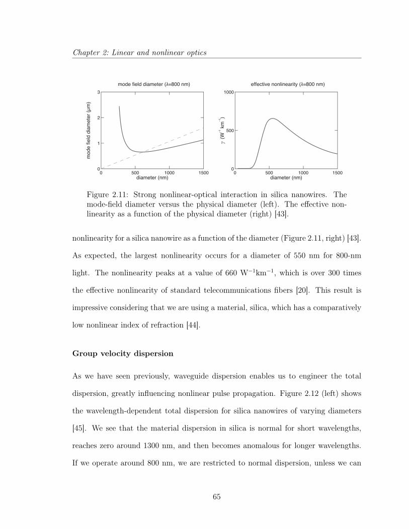
Chapter 2: Linear and nonlinear optics
diameter (nm)
mod
e fie
ld d
iam
eter
(μm
)
0 500 1000 1500
3
2
1
0
diameter (nm)
γ (W
–1 k
m–1)
0 500 1000 1500
1000
500
0
mode field diameter (λ=800 nm) effective nonlinearity (λ=800 nm)
Figure 2.11: Strong nonlinear-optical interaction in silica nanowires. Themode-field diameter versus the physical diameter (left). The effective non-linearity as a function of the physical diameter (right) [43].
nonlinearity for a silica nanowire as a function of the diameter (Figure 2.11, right) [43].
As expected, the largest nonlinearity occurs for a diameter of 550 nm for 800-nm
light. The nonlinearity peaks at a value of 660 W−1km−1, which is over 300 times
the effective nonlinearity of standard telecommunications fibers [20]. This result is
impressive considering that we are using a material, silica, which has a comparatively
low nonlinear index of refraction [44].
Group velocity dispersion
As we have seen previously, waveguide dispersion enables us to engineer the total
dispersion, greatly influencing nonlinear pulse propagation. Figure 2.12 (left) shows
the wavelength-dependent total dispersion for silica nanowires of varying diameters
[45]. We see that the material dispersion in silica is normal for short wavelengths,
reaches zero around 1300 nm, and then becomes anomalous for longer wavelengths.
If we operate around 800 nm, we are restricted to normal dispersion, unless we can
65

Chapter 2: Linear and nonlinear optics
counteract the normal dispersion with anomalous waveguide dispersion.
diameter (nm)
tota
l dis
pers
ion
(ns
nm–1
km–1
)
0 500 1000 1500
2.5
0
–2.5
–5.0
total dispersion versus diameter (λ=800 nm)
wavelength (nm)
tota
l dis
pers
ion
(ns
nm–1
km–1
)
0 500 1000 1500
1
0
–1
–2
800 nm 200 nm 400 nm 600 nm 800 nm
1200 nm
total dispersion for several diameters
material
Figure 2.12: Dispersion engineering in silica nanowires. The dispersion pa-rameter D versus wavelength for several waveguide dimensions (left). Thedispersion parameter D as a function of silica nanowire dimension for 800-nmlight (right) [45].
Figure 18 (right), shows the dispersion for 800-nm light as a function of nanowire
diameter [45]. For diameters of 700–1200 nm, strong anomalous waveguide dispersion
overcomes the material dispersion and results in anomalous total dispersion. For
diameters near 700 nm, total dispersion is very low. For even smaller dimensions, the
dispersion becomes extremely normal. This ability to tune the total dispersion is a
key element for engineering efficient nonlinear interactions.
2.4 Summary
We have shown the advantages of using sub-wavelength dielectric waveguides for
nonlinear optics. We have developed a theoretical basis for linear and nonlinear prop-
agation of continuous-wave and pulsed optical signals in free-space, within materials,
and using waveguides. We have seen how nano-scale, high-index contrast waveguides
66
Chapter 2: Linear and nonlinear optics
are capable of enhancing nonlinear interactions spatially using strong confinement
and temporally using tunable dispersion. Lastly, we have observed how to optimize
nonlinear interactions in a real photonic system. These principles serve the basis for
the proceeding chapters as we develop TiO2 photonics.
67
Chapter 3
Nonlinearities in bulk rutile TiO2
In this chapter, we study nonlinear refraction and multiphoton absorption in the bulk
TiO2 to establish a baseline that we can use when designing all-optical devices. Two-
photon absorption acts as the short-wavelength limit for many all-optical applications
and therefore, we investigate this around limit in TiO2 (800 nm). The interplay
between nonlinear refraction and absorption determines the usefulness of a nonlinear
material for all-optical processing. The Z-scan technique can characterize both of
these effects in a simple system. This chapter is divided into three section. First,
we will develop the theory of the Z-scan technique. Second, we will study nonlinear
refraction in bulk rutile TiO2 using the “closed-aperture” Z-scan technique. Lastly, we
will study multiphoton absorption using “open-aperture” Z-scan and evaluate TiO2
as a candidate material for all-optical applications.
68

Chapter 3: Nonlinearities in bulk rutile TiO2
3.1 The Z-scan technique
The Z-scan technique is popular technique to characterize nonlinear refraction and
absorption in bulk samples. It requires a single laser beam, can determine both
magnitude and sign of the nonlinearity, and is straightforward to analyze. The ex-
perimental and analytical simplicity of the Z-scan technique makes it an efficient
and powerful method to characterize bulk samples. We begin by discussing how to
measure nonlinear refraction using closed-aperture Z-scan.
aperture
detector
lens
laser in
Figure 3.1: A basic closed-aperture Z-scan setup consisting of a focusedbeam, an aperture, and a detector.
The setup of a typical Z-scan experiment is shown in Figure 3.1. It consists
of a focused Gaussian beam, an aperture, and a detector. We perform a Z-scan
measurement by scanning the sample through the focus and measuring the amount
of transmitted light that passes through the aperture with a photodetector (Figures
3.2 and 3.3). The location of the sample relative to the natural focus determines
the intensity incident on the sample and therefore, the strength of the nonlinear
lens created (self-focusing). This nonlinear lens changes the size of the beam in the
far-field, resulting in more or less power seen by the detector.
We can gain intuition for the Z-scan technique if we consider a positive n2
69
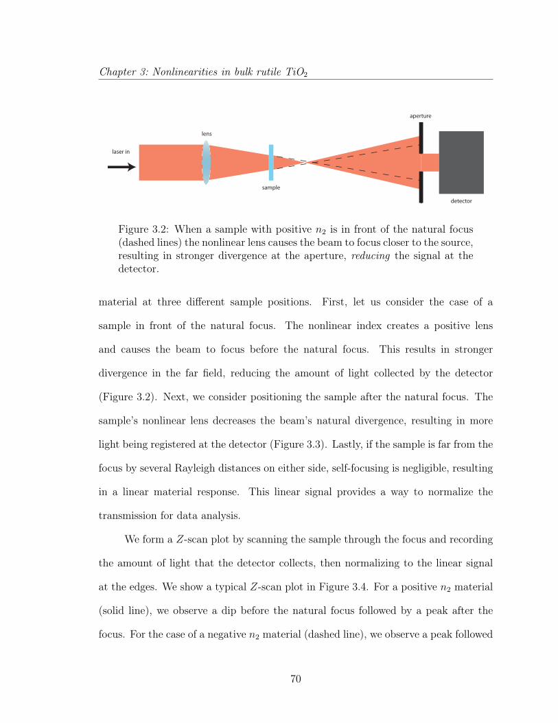
Chapter 3: Nonlinearities in bulk rutile TiO2
aperture
detector
lens
laser in
sample
Figure 3.2: When a sample with positive n2 is in front of the natural focus(dashed lines) the nonlinear lens causes the beam to focus closer to the source,resulting in stronger divergence at the aperture, reducing the signal at thedetector.
material at three different sample positions. First, let us consider the case of a
sample in front of the natural focus. The nonlinear index creates a positive lens
and causes the beam to focus before the natural focus. This results in stronger
divergence in the far field, reducing the amount of light collected by the detector
(Figure 3.2). Next, we consider positioning the sample after the natural focus. The
sample’s nonlinear lens decreases the beam’s natural divergence, resulting in more
light being registered at the detector (Figure 3.3). Lastly, if the sample is far from the
focus by several Rayleigh distances on either side, self-focusing is negligible, resulting
in a linear material response. This linear signal provides a way to normalize the
transmission for data analysis.
We form a Z-scan plot by scanning the sample through the focus and recording
the amount of light that the detector collects, then normalizing to the linear signal
at the edges. We show a typical Z-scan plot in Figure 3.4. For a positive n2 material
(solid line), we observe a dip before the natural focus followed by a peak after the
focus. For the case of a negative n2 material (dashed line), we observe a peak followed
70
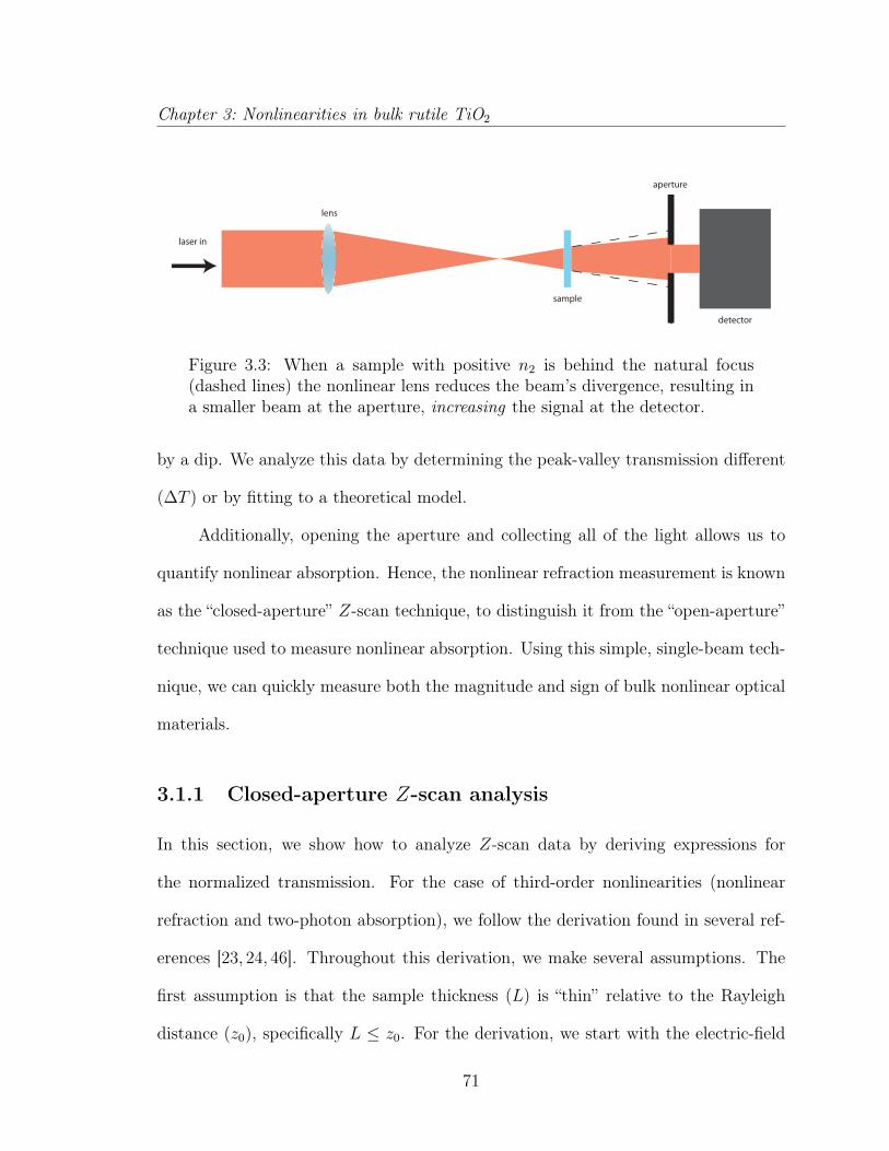
Chapter 3: Nonlinearities in bulk rutile TiO2
aperture
detector
lens
laser in
sample
Figure 3.3: When a sample with positive n2 is behind the natural focus(dashed lines) the nonlinear lens reduces the beam’s divergence, resulting ina smaller beam at the aperture, increasing the signal at the detector.
by a dip. We analyze this data by determining the peak-valley transmission different
(∆T ) or by fitting to a theoretical model.
Additionally, opening the aperture and collecting all of the light allows us to
quantify nonlinear absorption. Hence, the nonlinear refraction measurement is known
as the “closed-aperture” Z-scan technique, to distinguish it from the “open-aperture”
technique used to measure nonlinear absorption. Using this simple, single-beam tech-
nique, we can quickly measure both the magnitude and sign of bulk nonlinear optical
materials.
3.1.1 Closed-aperture Z-scan analysis
In this section, we show how to analyze Z-scan data by deriving expressions for
the normalized transmission. For the case of third-order nonlinearities (nonlinear
refraction and two-photon absorption), we follow the derivation found in several ref-
erences [23, 24, 46]. Throughout this derivation, we make several assumptions. The
first assumption is that the sample thickness (L) is “thin” relative to the Rayleigh
distance (z0), specifically L ≤ z0. For the derivation, we start with the electric-field
71

Chapter 3: Nonlinearities in bulk rutile TiO2
z/z0
norm
aliz
ed tr
ansm
ittan
ce
–8 –4 0 4 8
1.2
1.1
1.0
0.9
0.8
n2 < 0 n2 > 0
Figure 3.4: A typical Z-scan plot showing the normalized transmission versusz position for a material with n2 > 0 (solid line) and n2 < 0 (dashed line).
profile at the front interface within the sample E(Z, r, t) and calculate the nonlinear
phase and absorption accumulated during propagation through the sample, then ob-
tain the electric field at the exit Ee(Z, r, t). With this, we calculate how the exiting
beam will propagate to the far field where we place an aperture Ea(Z, r, t). We in-
tegrate over the aperture (r from 0 to the aperture radius ra) and then we integrate
in time to determine the amount of energy that reaches the detector. Finally, we
normalize this transmission to the transmitted energy with no nonlinearities present
to determine the normalized Z-scan transmission T (Z).
Closed-aperture derivation
We start with a focused Gaussian beam given by:
E (z, r, t) = E0 (t)w0
w (z)exp
[− r2
w2 (z)+ i
πr2
λR (z)+ iφ
], (3.1)
where E (z, r, t) is the complex amplitude and phase of the electric field within the
front surface of the sample, z is the sample position relative to the natural focus, r is
72

Chapter 3: Nonlinearities in bulk rutile TiO2
the radial distance, t is the time, E0 (t) is the on-axis time-dependent electric field,
w0 is beam waist, and with w (z) = w0
√1 + z2/z2
0 , where z0 = πw20/λ is the Rayleigh
distance and R (z) = z (1 + z20/z
2). In addition, φ is a constant phase term across
the beam profile and can be ignored here. We note that the power corresponding
to E(z, r, t) is the power before the sample, less the Fresnel reflection at the front
surface.
We have previously solved equation (2.81), which describes nonlinear absorp-
tion, and determined the intensity through propagation (equation (2.82)). With this,
we calculated the total nonlinear phase accumulated in equation (2.83). Rewriting
the intensity equation to include spatially varying intensity (through r and the sample
position z):
Ie (z, r, t) =I (z, r, t) e−αL
1 + q (z, r, t), (3.2)
and similarly, we rewrite the nonlinear phase equation as:
∆φ (z, r, t) =k0n2
α2
ln [1 + q (z, r, t)] . (3.3)
Here k0 = 2π/λ0 is the free space propagation constant, q (z, r, t) = α2I (z, r, t)Leff
and Leff is the effective length (equation (2.84)). We note that the on-axis phase shift
is given by:
∆Φ0 = ∆φ (z, 0, t) =k0n2
α2
ln [1 + q (z, 0, t)] , (3.4)
and, in the limit when α2 → 0, this becomes:
∆Φ0 = k0n2I0Leff , (3.5)
providing an easy way to calculate n2.
73

Chapter 3: Nonlinearities in bulk rutile TiO2
Using these expressions, the complex electric field at the exit of the sample:
Ee = E (z, r, t) e−αL/2(1 + q (z, r, t))(ik0n2/α2−1/2). (3.6)
For the case of a Gaussian beam and |q(z, r, t)| < 1, we can perform a binomial
expansion around q(z, r, t) to arrive at:
Ee(z, r, t) = E (z, r, t) e−αL/2∞∑m=0
Fm exp(2mr2/w2 (z)
), (3.7)
where
Fm =(i∆φ0 (z, r = 0, t))m
m!
m∏j=1
[1 + i
(j − 1
2
)λα2
2πn2
]. (3.8)
This expansion is known as the Gaussian decomposition method. Using this ex-
pression, we perform a zeroth-order Hankel transform to determine the electric field
distribution at the aperture at a distance d away:
Ea (r, t) = E (z, r = 0, t) e−αL/2∞∑m=0
Fmwm0
wmexp
[− r2
w2m
+iπr2
λRm
+ iθm
], (3.9)
with the following parameters:
w2m0 = w2(z)
2m+1, dm =
kw2m0
2, w2
m = w2m0
[g2 + d2
d2m
],
Rm = d[1− g
g2+d2/d2m
]−1
, θm = tan−1[
gd/dm
], g = 1 + d/R (z) .
(3.10)
Now, if the time-dependence is due to the power at the entrance of the sample P (t),
we can arrive at solutions for continuous-wave and pulsed transmission. First, we
integrate over the aperture:
TCW (z, P (t)) =
∫ ra0|Ea (z, r, P (t) , d)|2rdr∫ ra
0|Ea(z, r, P (t) , d)linear|
2rdr. (3.11)
We note that the denominator is the same as the numerator, except we take the limit
where n2 and multiphoton-absorption go to zero, thus it is the ratio of the power
74
Chapter 3: Nonlinearities in bulk rutile TiO2
with and without nonlinearities. If P (t) = constant, this is the solution for a laser
in continuous-wave operation. To arrive at the pulsed solution, we need to integrate
over time using:
Tpulsed (z, P (t)) =
∫∞−∞ P (t)TCW (z, P (t)) dt∫∞−∞ P (t)TCW (z, 0) dt
. (3.12)
This is the ratio of the energy with and without nonlinearities. It is essentially a
weighted average of transmission functions. We note that this model does not take
group velocity dispersion into account.
The distance d and the radius of the aperture ra are related through the S
parameter, which is the transmittance through the aperture. For a Gaussian beam,
the S parameter is:
S = 1− e(−2r2a/w
2a) (3.13)
with wa = w0(1 + d2/z20)
1/2. In the limit where S goes to unity, we arrive at the
open-aperture solution.
Closed-aperture simplifications
Although equations (3.9) and (3.11) are quite complicated, we can obtain immediate
insight if we take the limit when S → 0 for a very small aperture (d z0). This
can be accomplished by taking the limit when r → 0. Additionally, we assume the
nonlinear phase shift |∆Φ| 1. With these simplifications, we find equation (3.11)
becomes:
TCW (z,∆Φ0) ' 1 +4∆Φ0
(zz0
)(z2
z20
+ 9)(
z2
z20
+ 1) . (3.14)
This is a relatively good approximation. For example, using a ∆T of 50% corresponds
to an error of roughly 5%. Alternatively, we can find the peak and valley locations,
75

Chapter 3: Nonlinearities in bulk rutile TiO2
then look at the change in transmission to find an approximate value for the ∆Φ0:
∆Tp−v ' 0.406∆Φ0. (3.15)
In addition, we can calculate the peak-valley separation in the z-direction to be:
∆Zp−v ' 1.7Z0. (3.16)
These expressions serve as a quick method to estimate the Rayleigh distance and cal-
culate the nonlinear phase shift (and hence n2) of an unknown sample. We note that
for higher intensities, larger nonlinear phase shifts cause the signal to become asym-
metric and consequently, all of our analysis uses the full calculation using equations
(3.9), (3.11), and (3.12).
3.1.2 Open-aperture Z-scan analysis
Z-scan is a very convenient technique for measuring not only nonlinear refraction,
but nonlinear absorption using a small adjustment. By opening the aperture, S → 1,
and we collect all of the transmitted light. Here, nonlinear absorption is strongest at
the focus, appearing as a dip in the Z-scan plot. In this section, we provide a basic
analytical framework for measuring both two- and three-photon absorption in bulk
samples using the open-aperture Z-scan technique.
Open-aperture Z-scan with two-photon absorption
For two photon absorption, the open-aperture Z-scan derivation requires that we
determine the intensity change through a sample material for an arbitrary beam
waist and z location. For the simplest derivation, we assume that the beam does
76
Chapter 3: Nonlinearities in bulk rutile TiO2
not change its shape as it passes through the medium in the absence of two-photon
absorption and linear losses. This simply requires that the sample is smaller than
the Rayleigh distance. Using this approximation, for each point in the beam’s cross
section at the entrance of the material, there is a corresponding point at the exit
that is determined solely by the entrance intensity, linear and nonlinear loss, and the
length of the material. This also implies that our beam does not exhibit significant
self focusing within the material. Once we have this expression, we integrate over the
beam profile.
We begin our derivation with a Gaussian input profile:
Iin (z, r, P (t)) =2P (t)
πw2 (z)e−2r2
w2(z) , (3.17)
where P (t) is the instantaneous power of the beam at time t, r is the radial coordinate
and:
w (z) = w0
√1 +
(z
z0
)2
, (3.18)
is the beam waist at sample position z, where z = 0 is the focus. In addition, we
define the Rayleigh distance as z0 = πw20/λ. Now, we calculate the intensity at the
exit of the sample Ie(z, r, P (t)) using equation (3.2), and integrate over the area at
the exit of the sample to determine the transmitted power:
Pe (z, P (t)) = 2π
∫ ∞0
Iin (z, r, t) e−αL
1 + α2LeffIin (z, r, t)rdr = P (t) e−aL
ln (1 + q0 (z, P (t)))
q0 (z, P (t)),
(3.19)
where:
q0 (z, P (t)) =2α2Leffz0
λ (z2 + z20)P (t) =
α2Leffw20
w2 (z)I0 (t) . (3.20)
77

Chapter 3: Nonlinearities in bulk rutile TiO2
To determine the normalized transmission, we take the limit of this expression
as α2 → 0:
Plinear (z, t) = P (t) e−aL, (3.21)
then normalize equation (3.19) using this expression to arrive at the normalized trans-
mission:
T (z, P (t)) =ln (1 + q0 (z, P (t)))
q0 (z, P (t)). (3.22)
Equation (3.22) is a simple, closed-from expression for open-aperture Z-scan. If
P (t) is constant, this can be used for continuous-wave light. Most often, two-photon
absorption coefficients are very small, and therefore, pulsed light is necessary to obtain
measurable signal. Therefore, we integrate this equation as we have previously done
in equation (3.12).
Open-aperture Z-scan with three-photon absorption
We perform an identical procedure to the two-photon absorption case to derive three-
photon absorption. Now, we solve:
d
dlI (l) = −
(α1 + α3I
2 (l))I (l) , (3.23)
where l is the distance within the sample. This equation has a solution of:
Ie (z, r, t) =I (z, r, t) e−αL√
1 + 2α3Leff2I2 (z, r, t), (3.24)
where we have defined an effective length for three-photon absorption:
Leff2 ≡1− e−2αL
2α. (3.25)
78

Chapter 3: Nonlinearities in bulk rutile TiO2
Using equations (3.17), performing a similar integration to (3.19) and normal-
izing using (3.21), we arrive at the normalized transmission:
T (z, P (t)) =sinh−1 (q3 (z, P (t)))
q3 (z, P (t)), (3.26)
with
q3 (z, P (t)) =2√
2α3Leff2
λ
z0
z2 + z20
P (t) . (3.27)
Again, if P (t) is constant, this is the continuous-wave solution for three-photon ab-
sorption and we apply similar methods we used in the two-photon case to arrive at
pulsed solutions.
3.2 Nonlinear refraction in bulk rutile TiO2
We quantify nonlinear refraction in bulk rutile (TiO2) around 800 nm using the closed
aperture Z-scan technique. By fitting our data to theoretical models, we obtain
nonlinear refraction coefficients of n2 = 8.2× 10⁻¹⁹ for E⊥c and n2 = 9.7× 10⁻¹⁹ for
E||c. The strong nonlinearities observed in TiO2 around 800 nm are promising for
all-optical applications.
3.2.1 Introduction
Titanium dioxide (TiO2) possesses a high linear and nonlinear index of refraction
with minimal two-photon absorption for wavelengths longer than 800 nm, making
it a promising candidate material for integrated nonlinear optics applications [11,
44]. However, such devices often contain multiple materials in close proximity, which
makes isolating and studying a particular component material difficult. It is therefore
79

Chapter 3: Nonlinearities in bulk rutile TiO2
advantageous to quantify the optical nonlinearity of bulk TiO2 to facilitate the design
of integrated optical components.
TiO2 exists in several crystalline phases rutile, anatase and brookite, thus, es-
tablishing a reference value for the nonlinear index of refraction may be difficult.
These phases have similar bandgap energies (Eg) of 3.1 eV for rutile and brookite and
3.2 eV for anatase, with rutile being the most stable phase [47, 48]. Around 800 nm,
their indices of refraction range from 2.52 –2.79 in rutile, to 2.48 in anatase and 2.63 in
brookite [49–51]. Theoretically, the similar indices and bandgap energies should pro-
duce comparable optical nonlinearities [10,44,52]. Experimentally, reported values of
n2 in thin film anatase and rutile are similar when measured in the same study [53,54].
Even though all three phases should have consistent nonlinearities, their availability
in bulk form is very different. Reports on the optical properties anatase are nearly
restricted to powder or thin-film form and there are very few reports using brookite.
Meanwhile, high-quality single-crystal rutile is commercially available. The availabil-
ity and high quality of bulk rutile allow us to establish a robust value for the nonlinear
index of TiO2 that can be used as a first approximation for all-phases of TiO2.
In this study, we quantify nonlinear refraction in bulk rutile near 800 nm using
the closed-aperture Z-scan technique [23]. We fit our data to a theoretical model
to determine the nonlinear index of TiO2. These measurements, in conjunction with
nonlinear absorption measurements will allow us to calculate nonlinear figures of merit
for TiO2 in Section 3.3.
80

Chapter 3: Nonlinearities in bulk rutile TiO2
Table 3.1: Measured laser parameters
λ0 τ t z0 w0 d0 S M2 max I0
(nm) (fs) (mm) (mm) (µm) (m) GW/mm2
800 50 1.00 3.2 28 0.54 0.02 < 1.06 0.43
3.2.2 Experimental
We perform closed-aperture Z-scan measurements to quantify nonlinear refraction
in bulk rutile TiO2. We measure a 1-mm-thick single-crystal rutile sample grown
using the floating zone method, then cleaved along the (100) plane [55]. This cut
allows us to measure both the ordinary (E⊥c) and extraordinary (E||c) axes by
changing the crystal orientation. Our measured systems parameters are summarized
in Table 3.1. We use a chirped-pulse amplified Ti:Sapphire system with a full-width
at half-maximum (FWHM) pulse durations τ of 50 fs and energies up to 3 µJ at a
repetition rate of 250 kHz, similar to that described in [23]. We optimize dispersion
using a grating compressor and measure the pulse duration using frequency-resolved
optical gating (FROG) [56]. We spatially filter the beam to obtain a Gaussian profile,
then focus through 0.15-m focal length lens. A scanning slit detector on a single axis
stage measures the caustic (beam width versus z-position), which defines the beam
waist w0 and the quality factor (M2). A pick off mirror and a reference detector
before the lens allows us account for small power fluctuations [24].
We carry out a set of closed-aperture Z-scan measurements at several different
pulse energies for each orientation. Each measurement set consists of five different
Z-scan curves for different incident powers. Measurements taken at low irradiances
81

Chapter 3: Nonlinearities in bulk rutile TiO2
(0.02 GW/mm2) characterize linear signal caused by sample imperfections, which is
typically less than a few percent. We use these measurements to remove the linear
“background” signal from the four higher-power measurements. Additionally, we mea-
sure laser noise to be ±1–2 %. Using a reference detector reduces the system noise
to less than ±0.0015 in all but the lowest energy measurements.
3.2.3 Analysis methods
We fit our data to a standard theoretical model for thin samples to extract a value
of the nonlinear index of refraction (n2, defined using n = n0 + n2I) [23] [7]. Our
system has an S parameter of 0.02, which allows us to analyze our data in the S = 0
limit to within 0.5%. We assume a Guassian pulse shape and perform a weighted
average of continuous-wave solutions (see equation (3.12)). We note that this method
implicitly neglects chromatic dispersion in the sample, which we must correct for.
Our fit parameters are n2 and the waist location (as this is not determined during
measurement).
The strong material dispersion in TiO2 reduces the peak intensity, lowering the
apparent value of n2 if not accounted for. Using β2 = 985 fs2/mm for E⊥c and
β2 = 1240 fs2/mm for E||c for rutile around 800 nm, we calculate dispersion lengths
(τ 21/e/β2) of 0.9 and 0.7 mm (ordinary and extraordinary, respectively), where τ1/e is
the pulse duration measured from the 1/e point. These dispersion lengths are shorter
than our 1-mm sample and reduce the peak intensity by as much as 40% at the exit.
We incorporate group velocity dispersion into our model by rescaling the n2 value
extracted without GVD to reflect the effects of dispersion.
82
Chapter 3: Nonlinearities in bulk rutile TiO2
We calculate the GVD correction factor by first considering the duration (FWHM)
of a Gaussian pulse as it propagates:
τ (z) = τ0
√1 +
(4 ln 2
β2
τ 2L
)2
. (3.28)
For a material with negligible higher-order dispersion, the pulse will maintain its
Gaussian shape while becoming longer in duration. If there is negligible linear and
nonlinear absorption, the peak intensity within the sample is the intensity at the
entrance of the sample scaled by the duration:
I0 (z) = I0 (0)
(1 +
(4 ln 2
β2
τ 2L
)2)−1/2
. (3.29)
We calculate the nonlinear phase by integrating this expression over the sample length:
∆Φ0 = k0n2I0 (0)∫ L
0
(1 +
(4 ln 2β2
τ2 l)2)−1/2
dl
= k0n2I0 (0) τ2
β24 ln(2)sinh−1
(4 ln (2) β2
τ2L) . (3.30)
Our Z-scan measurement determines the nonlinear phase shift ∆Φ0, thus, we can
rescale our value of the nonlinear index of refraction without dispersion, nβ2=02 , to a
value that includes dispersion, nβ2 6=02 , using:
nβ2 6=02 = nβ2=0
2
β24 ln (2)L
τ 2sinh−1(4 ln (2) β2
τ2L) . (3.31)
This expression allows us to analyze our data using standard techniques, extracting
an effective nβ2=02 , then we scale this value to determine the actual nonlinear index
nβ2 6=02 that takes GVD into account.
3.2.4 Results and analysis
We present closed-aperture Z-scan measurements and theoretical fits for bulk rutile
in Figures 3.5 and 3.6 using ordinary (E⊥c) and extraordinary (E||c) polarizations
83

Chapter 3: Nonlinearities in bulk rutile TiO2
(respectively). We attribute the increased noise in the lowest powers measured to
the poor signal-to-noise ratio in the reference detector. These plots show a maximum
∆T of 58% for (E⊥c) and 62% for (E||c) when probed with the same pulse energy
(as measured before the sample). The birefringence we observe in the data should be
even stronger than it appears if we note that the higher index for E||c (n = 2.792)
results in a larger reflection off the front surface than for E⊥c (n = 2.52). From this
data, we see evidence of strong birefringence in the nonlinear index of refraction of
rutile.
z/z0
norm
aliz
ed tr
ansm
ittan
ce
–8 –4 0 4 8
1.4
1.2
1.0
0.8
0.6
3 nJ
9 nJ
15 nJ
28 nJ
Figure 3.5: Z-scan data and theoretical fit (solid lines) for bulk rutile TiO2
with E⊥c.
We find good agreement between our data and theoretical fits, shown in Figures
3.5 and 3.6. After correcting for group-velocity dispersion, we calculate n2 = 8.2 ×
10−19 for E⊥c and n2 = 9.7×10⁻¹⁹ for E||c. Subsequent open-aperture measurements
show that nonlinear absorption accounts for <2% of the measured ∆T , therefore, we
are justified neglecting multiphoton absorption and applying the dispersion correction
84

Chapter 3: Nonlinearities in bulk rutile TiO2
factors. These corrections result in a 16% and a 23% increase over the values we
calculate neglecting dispersion (E⊥c and E||c, respectively). Our analysis shows
an 18% birefringence in the nonlinear index of rutile, which may have important
consequences for devices made using single-crystal rutile.
z/z0
norm
aliz
ed tr
ansm
ittan
ce
–8 –4 0 4 8
1.4
1.2
1.0
0.8
0.6
3 nJ
9 nJ
15 nJ
28 nJ
Figure 3.6: Z-scan data and theoretical fit (solid lines) for bulk rutile TiO2
with E||c.
3.2.5 Discussion
We summarize reported values for bulk and thin film TiO2 in Table 3.2, along with
our measurements. Theory suggests that measurements using photon energies near
or below the half-bandgap (~ω = 1.55 eV, 800 nm) should be in reasonably good
agreement in terms of magnitude and sign [10, 52]. We find our measurements agree
well with reports using 1064 nm [44,57]. The 18% birefringence in the nonlinear index
may be partially attributed to the differences in the linear index, which predicts a
39% increase for E||c using an empirical model [44].
85

Chapter 3: Nonlinearities in bulk rutile TiO2
Table 3.2: Reported values of n2 in TiO2. Daggers (†) denote effective n2
values converted from third-harmonic measurements. Asterisks (∗) denotethis work.
form phase n2 (m2/W) λ0 (nm) index reference notesbulk rutile −1.1× 10⁻¹⁷ 532 2.97 [58] c||Ebulk rutile −1.0× 10⁻¹⁷ 532 2.66 [58] c⊥Ebulk rutile 9.7× 10⁻¹⁹ 800 2.79 [11] c||E∗bulk rutile 8.2× 10⁻¹⁹ 800 2.52 [11] c⊥E∗bulk rutile 9.4× 10⁻¹⁹ 1064 2.48 [44]bulk rutile 2× 10⁻¹⁸ 1064 2.48 [57]
thin film anatase −6.3× 10⁻¹⁷ 800 2.1 [53] PLDthin film rutile −2.7× 10⁻¹⁷ 800 2.3 [53] PLDthin film rutile 2.7× 10⁻¹⁸ 1900 2.4 [54] sol-gel†
thin film anatase 1.8× 10⁻¹⁸ 1900 2.29 [54] sol-gel†
thin film anatase 5.2× 10⁻¹⁸ 800 2.32 [59] sputtered†
nanocluster anatase 5.2× 10⁻¹⁸ 850 - [60]nanoparticle anatase 1× 10⁻¹⁹ 800 - [61]nanoporous anatase 2.2× 10⁻¹¹ 1064 1.9 [62]
While our measurements are consistent with other bulk rutile measurements,
they do not agree with reported thin-film values around 800 nm in either magnitude
or sign [53, 59]. This disagreement is even larger if we consider nanocluster, nano-
particle, and nanopourous thin-films of TiO2 [60–62]. Whereas the negative values
around 532 nm are consistent with theoretical models for direct-bandgap semicon-
ductors [10, 58], the negative values observed in thin-films around 800 nm are in-
consistent with theory [53]. These differences in reported n2 values may suggests a
different physical mechanism is responsible for the nonlinearities in thin films that is
not present in the bulk material [62]. Alternatively, these discrepancies may simply
reflect the experimental difficulty of working with thin films, which suffer from etalon
effects, nonlinear background signal caused by the substrate, and are susceptible to
damage [63,64]. Our values for n2 in bulk rutile TiO2 agree with other reported bulk
86

Chapter 3: Nonlinearities in bulk rutile TiO2
values, which suggests that different physical mechanisms may be responsible for the
nonlinearities in TiO2 thin films.
If we can integrate single-crystal rutile into devices, future designs should con-
sider the birefringence in n2, either to avoid potential problems or to take advantage
of this unique effect. This birefringence may produce a power-dependent polarization
rotation, potentially leading to unexpected results when used in conjunction with
polarization optics. Therefore, strategies to mitigate this nonlinear birefringence may
be necessary. Alternatively, designs which predominantly use E||c may benefit from
the increased value of n2. In addition, we may use this effect for nonlinear mode-
conversion or in new phase-matching schemes. The birefringence we observe in bulk
rutile may have important impacts for integrated nonlinear optical devices.
3.2.6 Nonlinear refraction summary
We quantify nonlinear refraction in bulk rutile around 800 nm using the closed-
aperture Z-scan technique. We measure strong nonlinearities that are 30 and 35
times those found in silica [21]. We observe an 18% birefringence in our measured
values of n2 that correlates with the higher linear index of refraction for E||c. By
studying bulk rutile, this study provides representative values for the nonlinear in-
dex of TiO2. These values, in conjunction with nonlinear absorption measurements,
provide a baseline to evaluate TiO2 for integrated nonlinear optical devices.
3.3 Multiphoton absorption in bulk rutile TiO2
The following paper appears in Optics Express 20 (3), 3118-3128, 2012.
87
Chapter 3: Nonlinearities in bulk rutile TiO2
Mixed two- and three-photon absorption in bulk
rutile (TiO2) around 800 nm
C. C. Evans,1 J. D. B. Bradley,1 E. A. Martì-Panameño,2 and Eric Mazur1
1School of Engineering and Applied Sciences, Harvard University,
9 Oxford Street, Cambridge, Massachusetts 02138, USA
2FCFM, Benemèrita Universidad Autònoma de Puebla, Av. San Claudio y Rio Verde,
C.P. 72570, Puebla, Puebla, Mèxico
Abstract: We observe mixed two- and three-photon absorption in bulk rutile (TiO2)
around 800 nm using the open aperture Z-scan technique. We fit the data with an
extended model that includes multiphoton absorption, beam quality, and ellipticity.
The extracted two- and three-photon absorption coefficients are below 1 mm/GW
and 2 mm3/GW2, respectively. We observe negligible two-photon absorption for 813-
nm light polarized along the extraordinary axis. We measure the nonlinear index of
refraction and obtain two-photon nonlinear figures of merit greater than 1.1 at 774
nm and greater than 12 at 813 nm. Similarly, we obtain three-photon figures of merit
that allow operational intensities up to 0.57 GW/mm2. We conclude that rutile is a
promising material for all-optical switching applications around 800 nm.
3.3.1 Introduction
Rutile (titanium dioxide) is a wide-bandgap semiconductor, advantageous for many
optical applications due to its high refractive index, birefringence, and transparency
for wavelengths ≥ 400 nm. In addition, it is naturally abundant, and highly stable.
88

Chapter 3: Nonlinearities in bulk rutile TiO2
Rutile also has a large Kerr nonlinearity (n2 = 9×10⁻¹⁹ m2/W) [44]. These properties
make rutile a promising material for nonlinear all-optical applications such as ultrafast
switching, logic [65] and wavelength conversion [66].
Even with a high Kerr nonlinearity, two- and three-photon absorption (2PA
and 3PA, respectively) impose limitations for nonlinear optical devices that rely on
high intensities [6]. For semiconductors, we expect 2PA (3PA) to occur for photon
energies equal to or greater than the half- (third-) bandgap energy (Eg) [9, 10]. The
half- (third-) bandgap energy corresponds to 800 nm (1200 nm) in rutile (Eg = 3.101
eV) [47]. We expect device properties to be strongly wavelength dependent around 800
nm due to the transition from pure 3PA to mixed two- and three-photon absorption.
Studies have quantified pure 2PA in bulk rutile for visible wavelengths (532–750
nm) [58,67,68] and 3PA for near-infrared wavelengths (1054 µm) [69]. In bulk rutile,
two-photon absorption was observed via weak luminescence for pump wavelengths
near 800 nm, however two-photon absorption coefficients were not reported [70].
Meanwhile, the nonlinear properties of TiO2 films [53, 54, 71–76] and TiO2 compos-
ites [71,72,74,75,77,78] have been extensively investigated. Of these thin film studies,
those that address pure-phase TiO2 near 800 nm report effective two-photon absorp-
tion coefficients that vary in both magnitude and sign [53,71,73–76]. However, there
are no reports on two-photon absorption in the bulk material using similar laser pa-
rameters for comparison. In addition, 3PA near 800 nm in bulk rutile has not been
reported. Therefore, our understanding of multiphoton absorption in bulk rutile is
incomplete and requires further study around 800 nm.
In this paper, we investigate multiphoton absorption near 800 nm in bulk rutile
89
Chapter 3: Nonlinearities in bulk rutile TiO2
using the open aperture Z-scan technique [23]. We develop a theoretical model to
fit the experimental data and extract two- and three-photon absorption coefficients
for different wavelengths and crystal orientations. Using the extracted multiphoton
absorption coefficients, we discuss nonlinear absorption processes near rutile’s half-
bandgap and evaluate its applicability as a material for all-optical devices.
3.3.2 Experimental
We perform open-aperture Z-scan measurements using two commercially available
1-mm-thick single-crystal rutile samples grown using the floating zone method [55].
One sample is cleaved along the (001) plane and the second is cleaved along the
(100) plane. The (001)-cut allows for measurements with the incident laser beam
polarized along the ordinary axis of the crystal (E⊥c), while the (100)-cut allows for
polarization along both the ordinary and extraordinary axes (E||c).
Our experimental setup is similar to that described in [23]. We use a chirped-
pulse amplified Ti:Sapphire system with pulse durations τ ≥ 50 fs, energies up to 3
µJ at a repetition rate of 250 kHz. We measure the pulse duration using frequency-
resolved optical gating (FROG). The beam is spatially filtered to obtain a Gaussian
shape then focused through a lens with a 0.15-m focal length. A scanning slit detector
on a single axis stage measures the caustic (beam width versus z-position). The
caustic determines the beam waist (wx0, wy0 in the x and y directions, respectively),
quality factor (M2) and ellipticity (wx0/wy0). A reference detector before the lens
allows us account for small power fluctuations [24]. We adjust the central wavelengths,
λ0, of the fs-pulses by spectrally filtering the seed using a physical aperture within
90
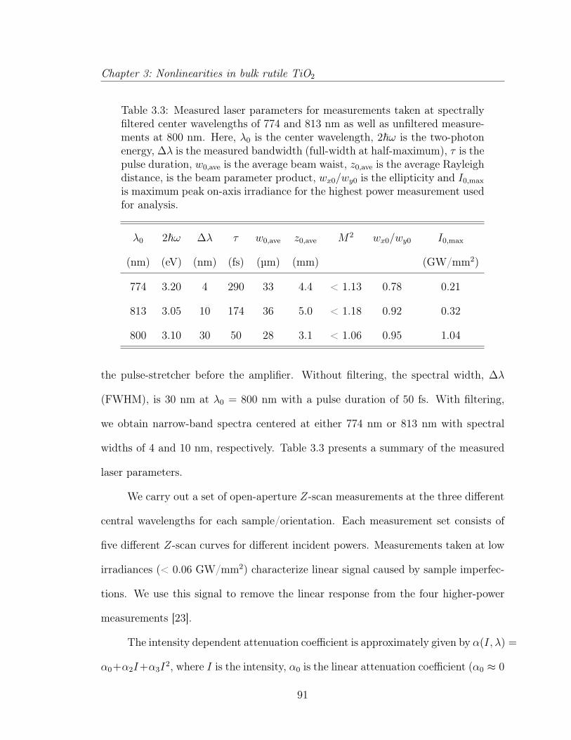
Chapter 3: Nonlinearities in bulk rutile TiO2
Table 3.3: Measured laser parameters for measurements taken at spectrallyfiltered center wavelengths of 774 and 813 nm as well as unfiltered measure-ments at 800 nm. Here, λ0 is the center wavelength, 2~ω is the two-photonenergy, ∆λ is the measured bandwidth (full-width at half-maximum), τ is thepulse duration, w0,ave is the average beam waist, z0,ave is the average Rayleighdistance, is the beam parameter product, wx0/wy0 is the ellipticity and I0,max
is maximum peak on-axis irradiance for the highest power measurement usedfor analysis.
λ0 2~ω ∆λ τ w0,ave z0,ave M2 wx0/wy0 I0,max
(nm) (eV) (nm) (fs) (µm) (mm) (GW/mm2)
774 3.20 4 290 33 4.4 < 1.13 0.78 0.21
813 3.05 10 174 36 5.0 < 1.18 0.92 0.32
800 3.10 30 50 28 3.1 < 1.06 0.95 1.04
the pulse-stretcher before the amplifier. Without filtering, the spectral width, ∆λ
(FWHM), is 30 nm at λ0 = 800 nm with a pulse duration of 50 fs. With filtering,
we obtain narrow-band spectra centered at either 774 nm or 813 nm with spectral
widths of 4 and 10 nm, respectively. Table 3.3 presents a summary of the measured
laser parameters.
We carry out a set of open-aperture Z-scan measurements at the three different
central wavelengths for each sample/orientation. Each measurement set consists of
five different Z-scan curves for different incident powers. Measurements taken at low
irradiances (< 0.06 GW/mm2) characterize linear signal caused by sample imperfec-
tions. We use this signal to remove the linear response from the four higher-power
measurements [23].
The intensity dependent attenuation coefficient is approximately given by α(I, λ) =
α0+α2I+α3I2, where I is the intensity, α0 is the linear attenuation coefficient (α0 ≈ 0
91

Chapter 3: Nonlinearities in bulk rutile TiO2
for λ = 800 nm in rutile), α2 is the 2PA coefficient, and α3 is the 3PA coefficient.
These coefficients are wavelength dependent. We extract multiphoton absorption co-
efficients by numerically fitting the measured data to a theoretical model that takes
into account the experimental beam and sample parameters (see Appendix A). Our
mixed multiphoton absorption model has four degrees of freedom (α2, α3, waist po-
sition, and astigmatism). Using this model, we fit the multiple Z-scan curves taken
at different peak irradiances simultaneously to extract a single value of α2 and α3 for
a given wavelength and polarization.
3.3.3 Results and discussion
Open aperture Z-scan measurements
Here, we show open aperture Z-scan measurements of bulk rutile for different incident
wavelengths and pulse durations. Figure 3.7 (left) shows a typical experimental open
aperture Z-scan curve in rutile for 800-nm, 50-fs pulses with E||c. Figure 3.7 (right)
shows the transmittance change (∆T = 1−T , at the focus) as a function of the peak
on-axis irradiance for the same sample and pulse duration (referred to here as a ∆T -
plot). Figure 3.8 shows data collected using λ0 = 774 nm and an input beam polarized
with E⊥c and E||c (Figs. 3.8, left and right, respectively). Similarly, Figures 3.9 and
3.10 show measurements and fits for λ0 = 813 nm and λ0 = 800, respectively.
The primary sources of uncertainty in our Z-scan measurements are the noise
of the laser and sample imperfections. We measure laser noise to be ±1–2 %. Using
low intensity and by adjusting the sample position, we reduce the linear background
variations caused by sample imperfections to less than 1%. To reduce the overall
92
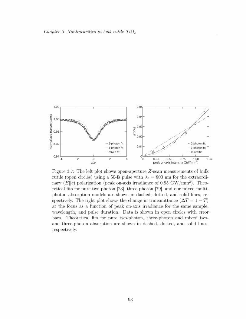
Chapter 3: Nonlinearities in bulk rutile TiO2
z/z0
norm
aliz
ed tr
ansm
ittan
ce
–4 –2 0 2 4
1.02
1.00
0.98
0.96
0.94
peak on-axis intensity (GW/mm2)
DT
(%)
0 0.25 0.50 0.75 1.00 1.25
0.05
0.04
0.03
0.02
0.01
0
Figure 3.7: The left plot shows open-aperture Z-scan measurements of bulkrutile (open circles) using a 50-fs pulse with λ0 = 800 nm for the extraordi-nary (E||c) polarization (peak on-axis irradiance of 0.95 GW/mm2). Theo-retical fits for pure two-photon [23], three-photon [79], and our mixed multi-photon absorption models are shown in dashed, dotted, and solid lines, re-spectively. The right plot shows the change in transmittance (∆T = 1− T )at the focus as a function of peak on-axis irradiance for the same sample,wavelength, and pulse duration. Data is shown in open circles with errorbars. Theoretical fits for pure two-photon, three-photon and mixed two-and three-photon absorption are shown in dashed, dotted, and solid lines,respectively.
93
Chapter 3: Nonlinearities in bulk rutile TiO2
noise, we use a reference photodiode, drift detection, temporal averaging, and back-
ground subtraction. These methods suppress the normalized transmittance variation
to ±0.0015. Consecutive scans resulted in measurements that were within this trans-
mittance variation. To characterize the repeatability of our technique, we analyzed
four measurement sets using E⊥c, taken over non-consecutive days for both the (001)-
and (100)-cut. We could not compare these measurements on a point-for-point basis,
consequently, we analyzed these measurement sets using our mixed two- and three-
photon model (see section A) and determined the standard deviation of α2 and α3.
We obtain a standard deviation of 5% for α2 and 18% for α3. In addition, we have
tested our system using CS2 with a 50-fs pulse at 800 nm and we obtain a 2PA co-
efficient of 0.06 mm/GW using standard analysis. This value falls within the range
of values obtained for CS2 in previous studies using 110-fs pulses [80,81] and thermal
methods [82,83].
Sample damage [63] and thermal effects [82,83] can mask electronic nonlineari-
ties. We verified that no damage or alterations occurred to the sample by comparing
low irradiance scans taken directly before and after each high intensity measurement
set. We performed thermally managed Z-scan [82, 83] using our bulk rutile samples
in both open- and closed-aperture configurations. By utilizing an optical chopper and
fast photodiodes to resolve pulse-to-pulse transmittance changes, we did not observe
cumulative (i.e. thermal) changes in the signal. Similarly, measurements taken at 10
kHz produced equivalent measurements to those taken at 250 kHz, confirming that
no cumulative effects were present.
94
Chapter 3: Nonlinearities in bulk rutile TiO2
Justification and fitting of the mixed-multiphoton absorption model
To establish the optimum fitting procedure, we first fit our data with standard open-
aperture Z-scan models and compare to our mixed-multiphoton absorption model.
Figure 3.7 (left) presents a typical experimental Z-scan curve that is fit using a pure
2PA-model [23], a pure 3PA-model [79] and our mixed-multiphoton model (dashed,
dotted, and solid lines, respectively). In Fig. 3.7 (right), we show an experimental
∆T -plot which is fit using a pure 2PA-, 3PA- and our mixed-multiphoton model
(dashed, dotted, and solid lines, respectively).
Comparing a pure 2PA to a pure 3PA model, we find that fitting individual Z-
scan curves appears to favor the 2PA model. However, a 2PA model predicts a very
different ∆T behavior with increasing irradiance. Three-photon absorption better fits
the high intensity ∆T data, yet is insufficient for low intensity data and individual
Z-scan curves. We see that our mixed-multiphoton model provides an excellent fit
to both Z-scan curves and ∆T -plots. These observations highlight two important
points. First, neither a pure 2PA- nor a pure 3PA-model can describe the data
sufficiently, necessitating a mixed-multiphoton absorption model. Second, both curve
fitting and the ∆T -plot method provide complimentary information. Curve fitting
is advantageous because signal away from the focus always contains the lowest order
absorption, such as 2PA. However, curve fitting can mask higher order absorption and
is susceptible to beam distortions. In contrast, the ∆T -plot provides a fast measure
on higher order absorption processes. Yet, this method may overlook lower order
absorption if sufficient low irradiance data is not included.
Quantifying mixed two- and three-photon absorption requires a balance between
95
Chapter 3: Nonlinearities in bulk rutile TiO2
the curve fitting and the ∆T -plot methods. It also requires further constraint to
account for the additional fitting coefficients. Consequently, we use a more robust
method whereby we fit an entire measurement set, consisting of several full Z-scan
curves taken at different peak irradiances, using a single set of parameters. This
technique produces equivalent results to the ∆T -plot method within the uncertainty.
We tested the optimization algorithm by using various starting points while
keeping all other parameters at experimentally determined values. These variations
included starting both α2 and α3 at zero as well as other magnitudes and signs of α2, α3
and the astigmatism. Other combinations, such as two- and four-photon absorption
(with astigmatism) could produce reasonable fits in some, but not all cases (notably
the 813-nm data set). We found that including two- and three-photon absorption in
our model resulted in good fits for all experimental data while minimizing the number
of fitted parameters.
We quantitatively compare the fit quality using standard 2PA [23] and 3PA [79]
models to our mixed-multiphoton model. Fitting a full data set (for example, a 50
fs pulse, E||c) using a 2PA or 3PA model produces R2 values of 0.974 and 0.925
for ±4 Rayleigh distance (respectively). We fit the same data set with our mixed-
multiphoton model and observe an R2 of 0.991 (solid lines, Fig. 3.10 right). We
performed a similar analysis with the 813-nm data set (E||c) and obtain R2 values
of 0.841, 0.944 and 0.950 (2PA, 3PA and mixed-multiphoton models, respectively).
From this analysis, the R2 correlation shows that the mixed-multiphoton model fits
the data better than either a pure two- or three-photon absorption model in all cases.
Therefore, we conclude that our mixed-multiphoton model is adequate for fitting our
96
Chapter 3: Nonlinearities in bulk rutile TiO2
experimental data and use this model to fit the Z-scan data in Figs. 3.8, 3.9, and
3.10 (shown in solid lines).
Two additional fitting parameters were included in the two- and three-photon
absorption fitting method. We fit the beam waist location, which aligns the model to
the experimental waist position. We found that fitting the astigmatism resulted in a
significant improvement in fit quality that we could not achieve by other means (i.e.
using additional multiphoton absorption terms or fitting the waist). However, the fit
astigmatism is relatively large, ranging from 25% to 100% of the measured Rayleigh
distance. We find the largest fit astigmatism using 50-fs pulses. Meanwhile, the
measured astigmatism is only up to 12% of the Rayleigh distance. This discrepancy
represents the largest source of uncertainty within our analysis. By including the
effects of fitting with and without the astigmatism, we estimate the uncertainty to
be ±15% in α2 and a factor of 2 for α3.
Two- and three-photon absorption coefficients
Table 3.4 summarizes bulk rutile two- and three-photon absorption coefficients. Over-
all, α2 ranges from less than 10−7 mm/GW to 0.9 mm/GW (±15%). Comparing 774
nm to 813 nm measurements, we find that the 2PA coefficients at these two wave-
lengths differ considerably. At 774 nm, α2 is 0.54 mm/GW (E⊥c) and 0.89 mm/GW
(E||c). At 813 nm and E||c, α2 is below the measureable limit. For E⊥c, we ex-
tract a value of 0.08 mm/GW. Lastly, two-photon absorption coefficients for 800 nm
are between the 774 nm and 813 nm coefficients. Rutile has typical values of α3
on the order of 1 mm3/GW2 as shown in Table 2. The values of α3 at 800 nm are
97
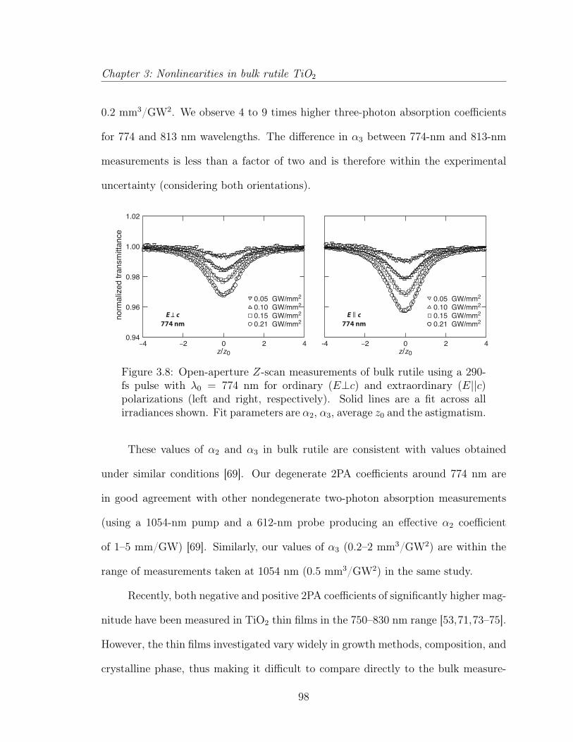
Chapter 3: Nonlinearities in bulk rutile TiO2
0.2 mm3/GW2. We observe 4 to 9 times higher three-photon absorption coefficients
for 774 and 813 nm wavelengths. The difference in α3 between 774-nm and 813-nm
measurements is less than a factor of two and is therefore within the experimental
uncertainty (considering both orientations).
774 nmE ± c
0.21 GW/mm20.15 GW/mm20.10 GW/mm20.05 GW/mm2
z/z0
-4 –2 0 2 4
E c774 nm 0.21 GW/mm2
0.15 GW/mm20.10 GW/mm20.05 GW/mm2
z/z0
norm
aliz
ed tr
ansm
ittan
ce
–4 –2 0 2 4
1.02
1.00
0.98
0.96
0.94
Figure 3.8: Open-aperture Z-scan measurements of bulk rutile using a 290-fs pulse with λ0 = 774 nm for ordinary (E⊥c) and extraordinary (E||c)polarizations (left and right, respectively). Solid lines are a fit across allirradiances shown. Fit parameters are α2, α3, average z0 and the astigmatism.
These values of α2 and α3 in bulk rutile are consistent with values obtained
under similar conditions [69]. Our degenerate 2PA coefficients around 774 nm are
in good agreement with other nondegenerate two-photon absorption measurements
(using a 1054-nm pump and a 612-nm probe producing an effective α2 coefficient
of 1–5 mm/GW) [69]. Similarly, our values of α3 (0.2–2 mm3/GW2) are within the
range of measurements taken at 1054 nm (0.5 mm3/GW2) in the same study.
Recently, both negative and positive 2PA coefficients of significantly higher mag-
nitude have been measured in TiO2 thin films in the 750–830 nm range [53,71,73–75].
However, the thin films investigated vary widely in growth methods, composition, and
crystalline phase, thus making it difficult to compare directly to the bulk measure-
98
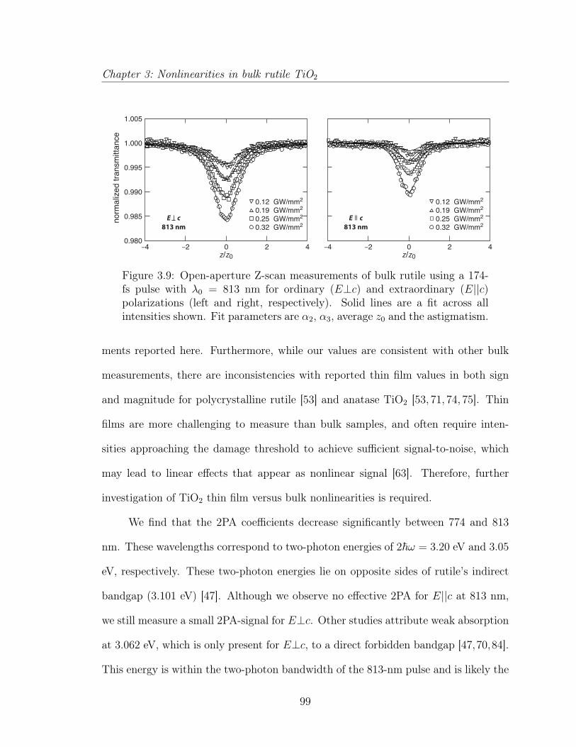
Chapter 3: Nonlinearities in bulk rutile TiO2
813 nmE ± c
0.32 GW/mm20.25 GW/mm20.19 GW/mm20.12 GW/mm2
z/z0
–4 –2 0 2 4
E c813 nm 0.32 GW/mm2
0.25 GW/mm20.19 GW/mm20.12 GW/mm2
z/z0
norm
aliz
ed tr
ansm
ittan
ce
–4 –2 0 2 4
1.005
1.000
0.995
0.990
0.985
0.980
Figure 3.9: Open-aperture Z-scan measurements of bulk rutile using a 174-fs pulse with λ0 = 813 nm for ordinary (E⊥c) and extraordinary (E||c)polarizations (left and right, respectively). Solid lines are a fit across allintensities shown. Fit parameters are α2, α3, average z0 and the astigmatism.
ments reported here. Furthermore, while our values are consistent with other bulk
measurements, there are inconsistencies with reported thin film values in both sign
and magnitude for polycrystalline rutile [53] and anatase TiO2 [53, 71, 74, 75]. Thin
films are more challenging to measure than bulk samples, and often require inten-
sities approaching the damage threshold to achieve sufficient signal-to-noise, which
may lead to linear effects that appear as nonlinear signal [63]. Therefore, further
investigation of TiO2 thin film versus bulk nonlinearities is required.
We find that the 2PA coefficients decrease significantly between 774 and 813
nm. These wavelengths correspond to two-photon energies of 2~ω = 3.20 eV and 3.05
eV, respectively. These two-photon energies lie on opposite sides of rutile’s indirect
bandgap (3.101 eV) [47]. Although we observe no effective 2PA for E||c at 813 nm,
we still measure a small 2PA-signal for E⊥c. Other studies attribute weak absorption
at 3.062 eV, which is only present for E⊥c, to a direct forbidden bandgap [47,70,84].
This energy is within the two-photon bandwidth of the 813-nm pulse and is likely the
99
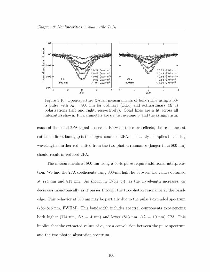
Chapter 3: Nonlinearities in bulk rutile TiO2
800 nmE ± c
z/z0
–4 –2 0 2 4
E c800 nm 1.04 GW/mm2
0.83 GW/mm20.63 GW/mm20.42 GW/mm20.21 GW/mm2
1.04 GW/mm20.83 GW/mm20.63 GW/mm20.42 GW/mm20.21 GW/mm2
z/z0
norm
aliz
ed tr
ansm
ittan
ce
–4 –2 0 2 4
1.02
1.00
0.98
0.96
0.94
Figure 3.10: Open-aperture Z-scan measurements of bulk rutile using a 50-fs pulse with λ0 = 800 nm for ordinary (E⊥c) and extraordinary (E||c)polarizations (left and right, respectively). Solid lines are a fit across allintensities shown. Fit parameters are α2, α3, average z0 and the astigmatism.
cause of the small 2PA-signal observed. Between these two effects, the resonance at
rutile’s indirect bandgap is the largest source of 2PA. This analysis implies that using
wavelengths further red-shifted from the two-photon resonance (longer than 800 nm)
should result in reduced 2PA.
The measurements at 800 nm using a 50-fs pulse require additional interpreta-
tion. We find the 2PA coefficients using 800-nm light lie between the values obtained
at 774 nm and 813 nm. As shown in Table 3.4, as the wavelength increases, α2
decreases monotonically as it passes through the two-photon resonance at the band-
edge. This behavior at 800 nm may be partially due to the pulse’s extended spectrum
(785–815 nm, FWHM). This bandwidth includes spectral components experiencing
both higher (774 nm, ∆λ = 4 nm) and lower (813 nm, ∆λ = 10 nm) 2PA. This
implies that the extracted values of α2 are a convolution between the pulse spectrum
and the two-photon absorption spectrum.
100

Chapter 3: Nonlinearities in bulk rutile TiO2
Table 3.4: Fitted nonlinear absorption coefficients, calculated 2PA figures ofmerit and maximum intensities from 3PA (using n2 = 7.9×10⁻¹⁹m2/W [85]).Here, λ0 is the center wavelength, 2~ω is the two-photon energy, α2 is the2PA coefficient, α3 is the 3PA coefficient, n2/(α2λ) is the 2PA figure of meritand I3PA
max is the maximum intensity calculated from the 3PA figure of merit,1 < [n2/(α3λImax)] [6]. The uncertainty for measurements at 774 nm and813 nm is ±15% for α2 and a factor of 2 for α3. For 800 nm, the uncertaintyis ±80% for α2 and a factor of 6 for α3.
ordinary polarization (E⊥c) extraordinary polarization (E||c)
λ0 2~ω α2 α3n2
α2λI3PA
max α2 α3n2
α2λI3PA
max
(nm) (eV)(mmGW
) (mm3
GW2
) ( GWmm2
) (mmGW
) (mm3
GW2
) ( GWmm2
)774 3.20 0.54 1.1 1.9 0.93 0.89 1.8 1.1 0.57
813 3.05 0.08 0.8 12.1 1.20 < 10−7 0.9 > 106 1.10
800 3.10 0.15 0.2 6.6 4.90 0.09 0.2 11.0 4.90
Nonlinear figures of merit
Multiphoton absorption has important implications for nonlinear optical devices. Ma-
terial performance is quantified by the nonlinear figures of merit [6]. The 2PA figure
of merit (FOM) is given by n2/(α2λ) and the 3PA FOM is given by n2/(α3λImax),
where Imax is the peak operational intensity. Both FOMs should be greater than unity
for all-optical applications. By setting the 3PA FOM equal to one, we calculate the
intensity at which 3PA becomes a limit, given by I3PAmax = n2/(α3λ). We measured the
nonlinear index of refraction around 800-nm (50-fs pulse) using closed-aperture Z-
scan and obtain a value of 7.9× 10⁻¹⁹ m2/W 1 using standard analysis methods [85].
Although theory predicts a resonant enhancement of the nonlinear index near the1This value is without the dispersion correction in Section 3.2.3. This is more applicable for the
present analysis as our nonlinear absorption model does not take dispersion into account either.
101
Chapter 3: Nonlinearities in bulk rutile TiO2
half-bandgap [10], we did not measure a significant deviation from values reported at
1064 nm [44], which may be due to dispersive broadening as explained in the previous
section. Therefore, the calculated nonlinear figures of merit should be considered a
lower limit. Using the nonlinear index and multiphoton absorption coefficients, we
evaluate rutile as a candidate material for all-optical applications around 800 nm by
calculating its nonlinear figures of merit.
Table 3.4 shows the calculated 2PA FOMs and I3PAmax for each measurement.
The 2PA FOMs at 774 nm are the lowest observed (1.9 and 1.1 for E⊥c and E||c,
respectively). At 813 nm, we obtain a FOM of 12.1 for E⊥c and greater than 106 for
E||c. Calculated I3PAmax is lowest for E||c using 774 nm, with a value of 0.57 GW/mm2,
and greater than 0.93 GW/mm2 for all other measurements.
All 2PA figures of merit calculated are greater than 1.1, which implies that rutile
is compatible with all-optical applications. Measurements at 813 nm show extremely
large FOMs, which is favorable for devices. We observe that 2PA can be neglected
at 813 nm (E||c) and expect similar results for E⊥c at longer wavelengths [86].
These FOMs imply compatibility with popular femtosecond pulsed sources such as
Ti:Sapphire and fiber lasers.
Although 2PA may be negligible for certain wavelengths, we must still avoid
significant 3PA by operating below I3PAmax . For the largest 3PA measured, I3PA
max is 0.57
GW/mm2 (E||c, 774 nm). This limit is far below thin-film damage thresholds for
TiO2 [87, 88] and provides a reasonable upper limit for integrated photonic devices
[89–92].
102
Chapter 3: Nonlinearities in bulk rutile TiO2
3.3.4 Conclusion
We observe mixed two- and three-photon absorption in bulk rutile around 800 nm. By
fitting open aperture Z-scan data to a numeric model, we separate the effects of mixed
multiphoton absorption. Two- and three-photon absorption coefficients are below 1
mm/GW and 2 mm3/GW2, respectively. Two-photon absorption falls below our
measurement capabilities for 174-fs pulse with a central wavelength of 813 nm (E||c).
We determine 2PA FOMs greater than 1 above and below rutile’s half-bandgap. We
expect superior performance for λ0 ≥ 813 nm, where the 2PA FOMs are greater
than 12.1. Additionally, 3PA is sufficiently small to enable all-optical applications for
intensities below 0.57 GW/mm2. From the low two- and three-photon absorption, we
conclude that rutile TiO2 is a promising material for all-optical applications such as
switching and logic near 800 nm.
3.3.5 Acknowledgements
Several people contributed to the work described in this paper. C.E. and E.M-P. con-
ceived of the basic idea for this work. C.E., E.M-P., and J.B. planned the experiments.
C.E. designed and carried out the experiments, implemented the model/fitting, and
analyzed the results. E.M., E.M-P. and J.B. supervised the research and the devel-
opment of the manuscript. C.E. wrote the first draft of the manuscript; all authors
subsequently took part in the revision process and approved the final copy of the
manuscript. Benjamin Franta, Phillip Munoz and Orad Reshef provided feedback on
the manuscript throughout its development. The research described in this paper
was supported by the NSF under contract ECCS-0901469. One of the authors, EM-
103

Chapter 3: Nonlinearities in bulk rutile TiO2
P, thanks CONACYT Mexico for the support through the project 120346, as well as
the David Rockefeller Center for Latin American Studies and the Mazur Group for
additional financial support.
104

Chapter 4
Optimizing TiO2 thin films
Fabricating integrated TiO2 optical devices requires high-quality thin films that can
serve low-loss planar waveguides, additionally, these films should have similar or im-
proved properties to bulk rutile in terms of their linear and nonlinear optical proper-
ties. Optimizing thin films, separate from fabricating nanowire devices, allows us to
isolate sources of loss attributed to the deposited film. This is particularly critical for
deposited materials, where there may be several sources of loss [93–96]. In this chap-
ter, we summarize a series of thin-film studies to develop and optimize amorphous and
polycrystalline (anatase phase) TiO2 thin films using reactive radio frequency (RF)
sputtering and then we compare representative films in Section 5.1.2. By develop-
ing suitable thin films, this provides us with a high-quality, well-understood starting
material from which we can fabricate integrated optical devices.
105
Chapter 4: Optimizing TiO2 thin films
4.1 Experimental
We deposited TiO2 thin films by reactive RF magnetron sputtering using a metallic
Ti target in an Ar and O2 atmosphere. We deposited the layers on 0.5-mm-thick
silicon substrates with a 2.2-µm-thick thermal oxide layer. We controlled the chamber
pressure, percentage of oxygen in the chamber given by the O2 flow rate/(Ar + O2
flow rates), as well as the substrate temperature. In addition, we either controlled
the applied power or DC substrate bias, the opposite parameter varies depending on
the specific conditions within the vacuum chamber. We conducted three studies: in
the first, we controlled the temperature to obtain either amorphous or anatase TiO2,
in the two remaining studies we optimized the oxygen percentage for each phase to
obtain high-quality TiO2 thin films.
4.1.1 Characterization methods
We summarize our thin-film characterization methods here.
Raman spectroscopy
The presence or absence of crystalline structure can lead to a large variation in optical
properties, including losses [97]. We determine which crystalline phases are present
in our deposited samples using micro Raman spectroscopy.
In Raman spectroscopy, photons are inelastically scattered by optical phonons in
a material, resulting in outgoing photons of lower energy (Stokes shift) that we detect
with a spectrometer. Mapping these energy shifts reveals which phonons are present
within the sample. Crystalline materials have long-range order that creates sharp
106
Chapter 4: Optimizing TiO2 thin films
Raman peaks while amorphous materials do not display discernible peaks. Using
Raman spectroscopy, we quickly characterize the crystallinity of our thin films.
Ellipsometry
We determine the thickness and index of refraction of our thin films using variable-
angle spectroscopic ellipsometry. Ellipsometry analyzes the outgoing polarization of
light reflected from the surface of a sample. By performing a series of measurements
at different wavelengths, polarization, and angles, we can fit the resulting data to a
model in order to extract the thickness and optical constants of our planar sample.
We determine the index of refraction over the wavelength range of 600–1700 nm
by fitting spectroscopic ellipsometry data to a Sellmeier model, given by:
n2 (λ) = 1 +B1λ
2
λ2 − C1
+B2λ
2
λ2 − C2
+B3λ
2
λ2 − C3
. (4.1)
Here, λ is the wavelength (in µm) and the Bn’s and Cn’s are fitting coefficients. This
relation provides us with the refractive index across a wide wavelength range that we
can use to quantify dispersion in our nanowire devices.
Prism coupling
Prism coupling is a complimentary technique to spectroscopic ellipsometry that, in
addition to estimating index and thickness, allows us to measure planar optical prop-
agation losses [98]. In prism coupling, we press a prism against the film under test,
forming a point of close contact. Next, we shine laser through the prism to this
contact point. Now, we rotate the prism-film system causing light to encounter the
prism-film interface at different angles. If the angle corresponds to an angle asso-
107
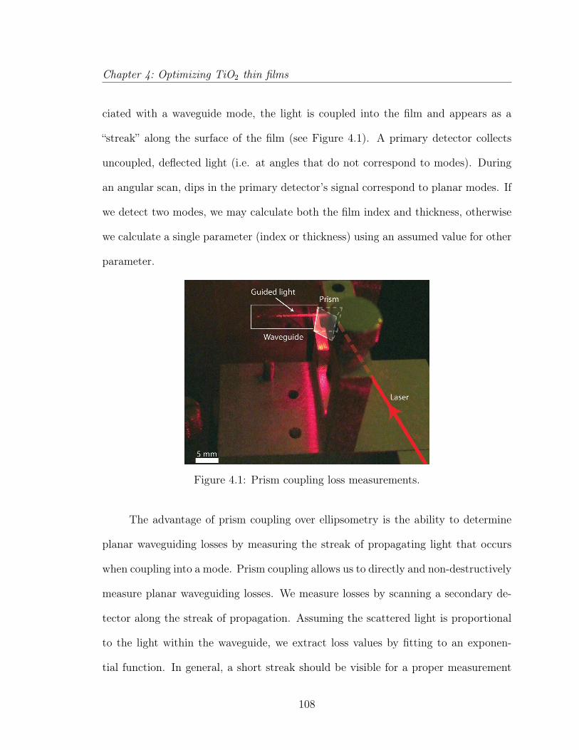
Chapter 4: Optimizing TiO2 thin films
ciated with a waveguide mode, the light is coupled into the film and appears as a
“streak” along the surface of the film (see Figure 4.1). A primary detector collects
uncoupled, deflected light (i.e. at angles that do not correspond to modes). During
an angular scan, dips in the primary detector’s signal correspond to planar modes. If
we detect two modes, we may calculate both the film index and thickness, otherwise
we calculate a single parameter (index or thickness) using an assumed value for other
parameter.
Figure 4.1: Prism coupling loss measurements.
The advantage of prism coupling over ellipsometry is the ability to determine
planar waveguiding losses by measuring the streak of propagating light that occurs
when coupling into a mode. Prism coupling allows us to directly and non-destructively
measure planar waveguiding losses. We measure losses by scanning a secondary de-
tector along the streak of propagation. Assuming the scattered light is proportional
to the light within the waveguide, we extract loss values by fitting to an exponen-
tial function. In general, a short streak should be visible for a proper measurement
108
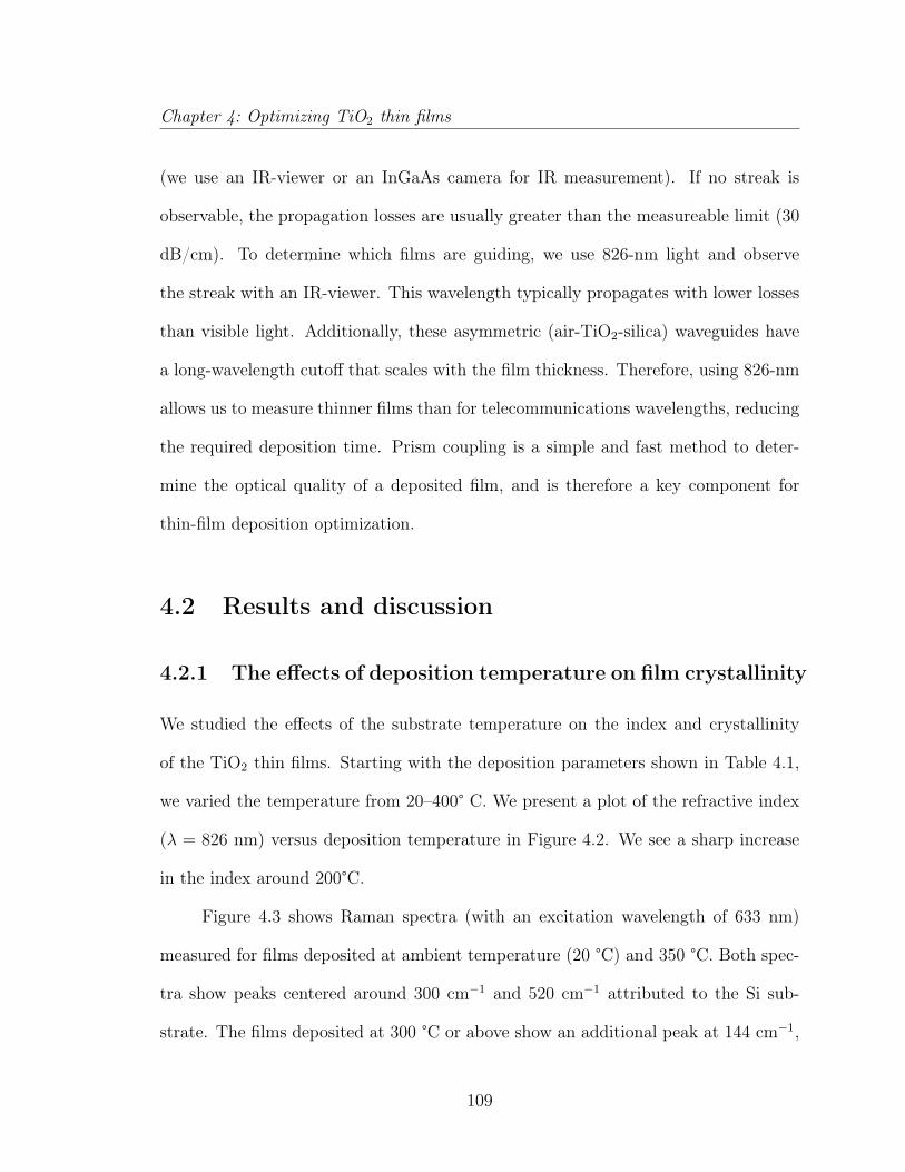
Chapter 4: Optimizing TiO2 thin films
(we use an IR-viewer or an InGaAs camera for IR measurement). If no streak is
observable, the propagation losses are usually greater than the measureable limit (30
dB/cm). To determine which films are guiding, we use 826-nm light and observe
the streak with an IR-viewer. This wavelength typically propagates with lower losses
than visible light. Additionally, these asymmetric (air-TiO2-silica) waveguides have
a long-wavelength cutoff that scales with the film thickness. Therefore, using 826-nm
allows us to measure thinner films than for telecommunications wavelengths, reducing
the required deposition time. Prism coupling is a simple and fast method to deter-
mine the optical quality of a deposited film, and is therefore a key component for
thin-film deposition optimization.
4.2 Results and discussion
4.2.1 The effects of deposition temperature on film crystallinity
We studied the effects of the substrate temperature on the index and crystallinity
of the TiO2 thin films. Starting with the deposition parameters shown in Table 4.1,
we varied the temperature from 20–400° C. We present a plot of the refractive index
(λ = 826 nm) versus deposition temperature in Figure 4.2. We see a sharp increase
in the index around 200°C.
Figure 4.3 shows Raman spectra (with an excitation wavelength of 633 nm)
measured for films deposited at ambient temperature (20 °C) and 350 °C. Both spec-
tra show peaks centered around 300 cm−1 and 520 cm−1 attributed to the Si sub-
strate. The films deposited at 300 °C or above show an additional peak at 144 cm−1,
109

Chapter 4: Optimizing TiO2 thin films
Table 4.1: Deposition parameters for TiO2 temperature dependence study.
temperature∗ power DC bias pressure O2 flow time
(°C) (W) (V) (mTorr) (% of total) (min)
20–400∗ not controlled 300 2 10 90
consistent with the anatase phase of TiO2 [99]. The films deposited at ambient tem-
perature show no discernible peaks associated with the known crystalline phases of
TiO2. Therefore, we expect those layers to be primarily amorphous. We represent
the depositions with discernible anatase peaks as filled circles in Figure 4.2.
temperature (°C)
refr
activ
e in
dex,
λ =
826
nm
0 100 200 300 400 500
2.42
2.40
2.38
2.36
2.34
2.32
anatase
amorphous
Figure 4.2: The effects of the substrate temperature on the refractive indexof TiO2 films.
This deposition study shows that temperatures of 300°C and above facilitates
the crystallization of TiO2 into the anatase phase. This transition temperature is
consistent with other reports [100]. Additionally, the higher index of refraction is
correlated to the crystallinity. Using the deposition temperature, we are able to
control the crystallinity of our films to produce anatase or amorphous TiO2. From
110

Chapter 4: Optimizing TiO2 thin films
this point forward, we separate our deposition studies by substrate temperature to
optimize these two varieties of TiO2.
TiO2
100 nm
TiO2
639 cm–1
Raman shift (cm–1)
inte
nsity
(a.u
.)
100 300 500 700
520 cm–1 (Si)
520 cm–1 (Si)
300 cm–1 (Si)
300 cm–1 (Si) 399 cm–1
141 cm–1 350 ºC
20 ºC
Figure 4.3: Raman spectroscopy of TiO2 thin films deposited at two substratetemperatures. The film deposited at ambient temperature (top) displaysonly peaks attributed to the silicon substrate. The film deposited at 300 °C(bottom) shows peaks associated with the anatase crystalline phase of TiO2.
4.2.2 Optimizing amorphous TiO2 films
We optimized our amorphous TiO2 films by controlling the oxygen flow rate, then
study its effects on refractive index, deposition rate, and optical propagation losses.
Our deposition parameters are summarized in Table 4.2. Figure 4.4 (left) shows the
refractive index versus O2 flow rate and Figure 4.4 (right) shows the deposition rate
versus O2 flow rate. We observed wave guiding (for λ = 826 nm) only in the film
deposited with an O2 flow rate of 10 % (notated with filled circles).
We see three interesting features in this data. First, we observe that an increased
O2 flow rate greatly reduced the deposition rate. Second, the refractive index is very
111

Chapter 4: Optimizing TiO2 thin films
Table 4.2: Deposition parameters for amorphous TiO2 oxygen flow-rate op-timization.
temperature power DC bias pressure O2 flow time
(°C) (W) (V) (mTorr) (% of total) (min)
20 200 power dependent 2 2 –20 90
similar for all films with O2 flow rates from 5–20%. Lastly, only film deposited at a
10% O2 flow rate exhibited guiding. The film deposited at an O2 flow rate of 20%
was 40-nm thick and was therefore too thin to support a guided mode due to the
asymmetrical waveguide formed by the silica-TiO2-air stack. A longer deposition at
this flow rate may also produce high-quality TiO2 films, however the deposition rate
is very slow, making proper optimization a time-consuming and costly process. The
10% O2 process is also very consistent, for example, over 20 separate depositions using
this process, the average index around 826 nm was 2.356±.024. Although further
optimization may be possible, our results using a 10% O2 flow rate are sufficient for
many of the first devices in TiO2.
The films deposited with a 10% O2 flow rate have a high refractive index and
exhibit low loss. The index typically varies between 2.29–2.40 between 632 –1550 nm.
The Sellmeier equation for this amorphous TiO2 recipe is:
n2 (λ) = 1 +3.3977λ2
λ2 − 0.045576+
0.76661λ2
λ2 − 0.062507, (4.2)
where λ is the wavelength in µm. This film has relatively strong material dispersion
of −2300 ps/nm/km around 800 nm. The dispersion reduces to −260 ps/nm/km
around 1550 nm, which is lower than silicon around 1550 nm (−900 ps/nm/km).
112

Chapter 4: Optimizing TiO2 thin films
oxygen partial flow (%)
refr
activ
e in
dex
0 5 10 15 20 25
2.40
2.35
2.30
2.25
oxygen partial flow (%)
depo
sitio
n ra
te (n
m/m
in)
0 5 10 15 20 25
2.5
2.0
1.5
1.0
0.5
0
guiding
non-guiding
Figure 4.4: Refractive index (left) and deposition rate (right) versus O2 flowrate for TiO2 films deposited at 20 °C. Filled circles indicate that guidingwas observed using a wavelength of 826 nm.
We show the wavelength-dependent losses of a 250-nm thick film in Figure 4.5.
Shorter wavelengths have higher losses that decrease and reach a constant value of
0.4 dB/cm from 1310–1550 nm. The sharp increase in losses at short wavelengths is
consistent with theoretical models that consider surface scattering alone [98].
wavelength (nm)
loss
(dB/
cm)
600 800 1000 1200 1400 1600
1.5
1.0
0.5
0
Figure 4.5: Wavelength dependent planar waveguiding losses in a 250-nmthick amorphous TiO2 film.
113

Chapter 4: Optimizing TiO2 thin films
4.2.3 Optimizing anatase TiO2 films
We performed a series of depositions to optimize the O2 flow rate using temperatures
greater than 200 °C with parameters presented in Table 4.3. We show the index and
deposition rate as a function of O2 flow rate in Figure 4.6 (left and right, respectively).
Table 4.3: Deposition parameters for amorphous TiO2 oxygen flow-rate op-timization.
temperature power DC bias pressure O2 flow time
(°C) (W) (V) (mTorr) (% of total) (hours)
200–350 130–200 power dependent 2 10–33 1.5–36
There is considerable variability in the quality of the deposited films. Aside
from one film, only films deposited with O2 flow rates of 33% guided around 826 nm.
Of the three guiding films with an O2 flow rate of 33%, the 77-nm thick film displayed
losses of 4.5 dB/cm, meanwhile 100-nm and 250-nm thick films had losses of 15 and
20 dB/cm, respectively.
We were unable to extend the low loss achieved in the thinnest film to thicker
films. Therefore, the low losses in the 77-nm thick film are likely due to weak confine-
ment, allowing the wave to travel predominantly in the low-loss SiO2 undercladding.
Additionally, we observe an increased loss of 21 dB/cm for oxygen flow rates of 27%
(100-nm thick).
Although additional optimization may be possible, we have focused predomi-
nantly on an O2 flow rate of 33%. We note that the deposition rate of anatase is
highly dependent on the O2 flow rate. Unfortunately, a flow rate of 33% results in
exceptionally long deposition times (for example, the 250-nm film was deposited for
114

Chapter 4: Optimizing TiO2 thin films
oxygen partial flow (%)
depo
sitio
n ra
te (n
m/m
in)
0 10 20 30 40
2.5
2.0
1.5
1.0
0.5
0
guiding
non-guiding
oxygen partial flow (%)
refr
activ
e in
dex
0 10 20 30 40
2.48
2.44
2.40
2.36
2.32
2.28
guiding
non-guiding
Figure 4.6: Refractive index (left) and deposition rate (right) versus O2 flowrate for TiO2 films deposited at 350 °C (films deposited at 10% O2 flow ratehad a substrate temperature between 200–300 °C). Filled circles indicate thatguiding was observed with using a wavelength of 826 nm.
over 23 hours). The narrow window and slow deposition rates dramatically affect our
ability to conduct a proper study.
Anatase films deposited with a substrate temperature of 350 °C and an oxygen
flow rate of 33% exhibit higher indices of refraction than our amorphous films. The
index of refraction ranges from 2.41–2.52 between 632 –1550 nm. The Sellmeier
equation for a typical film is given here:
n2 (λ) = 1 +3.3973λ2
λ2 − 0.0392+
1.3204λ2
λ2 − 0.062776. (4.3)
Although the index is higher in anatase than amorphous TiO2, the group velocity dis-
persion is experimentally identical in both films. The higher index in anatase enables
slightly stronger dispersion engineering for integrated nonlinear optical devices.
We present the wavelength dependent losses for a 250-nm thick anatase film in
Figure 4.7. We notice that the losses are very high for visible wavelengths and dras-
tically decrease to 4.2 dB/cm around 1550 nm. Although these longer wavelengths
115

Chapter 4: Optimizing TiO2 thin films
wavelength (nm)
loss
(dB/
cm)
600 800 1000 1200 1400 1600
40
30
20
10
0
Figure 4.7: Wavelength dependent planar waveguiding losses in a 250-nmthick anatase TiO2 film.
have increasingly lower losses, they do not appear to reach a constant value as we
observed in the amorphous film. The dominant loss mechanism may be due to the
poly-crystallinity of our films, which is apparent in Figure 5.2b and after channel
waveguide etching in Figure 5.3b. From this trend, we expect significantly improved
performance for mid-infrared wavelengths.
4.3 Conclusion
We have deposited two varieties of TiO2 planar waveguides with typical propagation
losses at 826 nm of 0.6 dB/cm (amorphous thin films) and 20 dB/cm (anatase thin
films). The losses are as low as 0.4 and 4.2 dB/cm around 1550 nm (amorphous and
anatase, respectively). The low losses and high refractive index confirm that these
TiO2 films are useful for integrated nanophotonic devices. Although the anatase phase
116

Chapter 4: Optimizing TiO2 thin films
is slightly higher in index, the losses in our amorphous TiO2 films are significantly
lower. Based on these results, amorphous TiO2 appears to have a distinct advantage
for linear optical applications.
117
Chapter 5
Linear optical properties of integrated
TiO2 waveguides and devices
In this chapter, we present two papers that explore the linear optical properties of
integrated TiO2 waveguides and devices. The first paper presents additional details
on representative amorphous and polycrystalline-anatase TiO2 not included in Chap-
ter 4, then develops linear waveguides, bends, and directional couplers. The second
paper presents integrated optical resonators for visible wavelengths. These linear
devices serve as the basis for more complex linear and nonlinear devices.
5.1 Linear waveguides
The following paper appears in Optics Express 20, 23821-23831, 2012.
118

Chapter 5: Linear optical properties of integrated TiO2 waveguides and devices
Submicrometer-wide amorphous and polycrystalline
anatase TiO2 waveguides for microphotonic devices
J. D. B. Bradley, C. C. Evans, J. T. Choy, O. Reshef, P. B. Deotare,
F. Parsy, K. C. Phillips, M. Lončar, and E. Mazur
School of Engineering and Applied Sciences, Harvard University,
9 Oxford Street, Cambridge, Massachusetts 02138, USA
Abstract: We demonstrate amorphous and polycrystalline anatase TiO2 thin films
and submicrometer-wide waveguides with promising optical properties for micropho-
tonic devices. We deposit both amorphous and polycrystalline anatase TiO2 using
reactive sputtering and define waveguides using electron-beam lithography and reac-
tive ion etching. For the amorphous TiO2, we obtain propagation losses of 0.12±0.02
dB/mm at 633 nm and 0.04 ± 0.01 dB/mm at 1550 nm in thin films and 2.6 ± 0.5
dB/mm at 633 nm and 0.4 ± 0.2 dB/mm at 1550 nm in waveguides. Using single-
mode amorphous TiO2 waveguides, we characterize microphotonic features including
microbends and optical couplers. We show transmission of 780-nm light through mi-
crobends having radii down to 2 µm and variable signal splitting in microphotonic
couplers with coupling lengths of 10 µm.
5.1.1 Introduction
The development of nanoscale optical waveguides with low losses has led to miniature,
efficient photonic devices for applications in the fields of communications, computing,
metrology, and sensing [101–108]. Nanoscale waveguides strongly confine light by
119
Chapter 5: Linear optical properties of integrated TiO2 waveguides and devices
utilizing high-refractive-index-contrast materials, resulting in high optical intensities
for efficient nonlinear light-matter interactions [109–111], small bending radii, and
microscale device footprints [112, 113]. Furthermore, controlling nanoscale features
enables one to engineer critical waveguide properties, such as the number of sup-
ported modes, the strength of signal coupling between adjacent waveguides, effective
nonlinearity, and waveguide dispersion [43,114].
Standard nanoscale waveguide materials, such as silica and silicon, have limi-
tations despite their low cost and compatibility with current photonic and electronic
platforms. Fiber-based silica nanowires have limited scalability due to labor-intensive
assembly [112]. Meanwhile silicon, a scalable material with mature fabrication pro-
cesses, offers transparency only at wavelengths above 1.1 µm. Limited transparency
inhibits its use in emerging applications such as quantum photonics, where promising
single-photon sources emit at visible wavelengths [115]. Silicon also exhibits strong
two-photon absorption at telecommunications wavelengths, which leads to free-carrier
absorption and prohibits many nonlinear devices [7, 92, 111]. Therefore, we require
complimentary nanoscale waveguide materials to meet the demands of future visible
and near infrared linear and nonlinear microphotonic systems.
Recently titanium dioxide (TiO2) has attracted attention as a prospective pho-
tonic material [116–122]. Amorphous and polycrystalline TiO2 thin films can be
deposited at low temperatures (< 650 K) using conventional, scalable methods [97],
allowing for straightforward integration with other on-chip devices [123]. TiO2 has a
high refractive index (n ≈ 2.4), which allows for high-refractive-index-contrast waveg-
uides and strong light confinement. Due to its large bandgap (Eg = 3.1 eV), TiO2 is
120
Chapter 5: Linear optical properties of integrated TiO2 waveguides and devices
transparent over a broad wavelength range that includes the visible and near-infrared.
In addition, TiO2 is a promising nonlinear photonic material, having a high nonlin-
earity (≥ 25 times higher than silica) [11, 44, 53] and low two-photon absorption for
wavelengths above 800 nm [11]. This combination of properties puts TiO2 into a
similar class as silicon nitride; however, TiO2 exhibits both a higher linear refractive
index (2.4 for TiO2 versus 2.0 for silicon nitride at 800 nm) and nonlinear refractive
index (9 × 10⁻¹⁹ m2/W for bulk rutile TiO2 versus 2.4 × 10⁻¹⁹ m2/W for silicon
nitride) [44, 124].
Amorphous TiO2 waveguides on oxidized silicon [119,121] and waveguides formed
in single-crystal rutile [120, 122] have been demonstrated. The reported amorphous
waveguide structures were limited to large dimensions (> 1 µm) [119] or only in-
vestigated for visible-wavelength operation [121]. For practical on-chip devices, such
waveguides must have submicrometer dimensions to support single-mode operation.
Small dimensions are also necessary for flexibility in the design of basic features such
as waveguide bends and optical couplers on the microscale. In addition, anatase mi-
crophotonic waveguides have not been developed, despite having a higher reported
nonlinearity [53] and requiring lower fabrication temperatures than crystalline rutile
waveguides.
In this paper, we report on TiO2 strip waveguides with submicrometer dimen-
sions and promising optical properties for on-chip photonic devices. We fabricate
both amorphous and polycrystalline anatase TiO2 thin films and compare their struc-
tural and optical properties. We then fabricate strip waveguides and measure their
propagation losses at visible and near-infrared wavelengths. Finally, we investigate
121

Chapter 5: Linear optical properties of integrated TiO2 waveguides and devices
Table 5.1: Reactive RF sputtering parameters applied to deposit 0.25-µm-thick amorphous and polycrystalline anatase TiO2 films.
deposition parameter amorphous TiO2 anatase TiO2
temperature (K) 290 625pressure (mTorr) 2 2Ar flow (sccm) 40 40O2 flow (sccm) 4.4 20RF power (W) 158 200time (min.) 300 1390
microphotonic features to assess the prospective application of TiO2 waveguides in
photonic devices.
5.1.2 TiO2 thin films
Thin-film deposition
We deposit TiO2 thin films on oxidized silicon substrates (3-µm-thick SiO2) using
reactive radio frequency (RF) magnetron sputtering. We prepare 0.25-µm-thick TiO2
films under the conditions summarized in Table 5.1. Films deposited at a substrate
temperature of 290 K and 625 K yield amorphous and anatase TiO2 thin-films, respec-
tively [97]. We select optimal O2 flow rates and RF powers to obtain stoichiometric,
highly transparent TiO2 thin films [118].
Thin-film characterization
We determine the crystalline structure of the TiO2 thin films using Raman spec-
troscopy. To avoid background signal from the silicon substrate, we measure Raman
spectra of thin films deposited on glass substrates using identical deposition param-
122
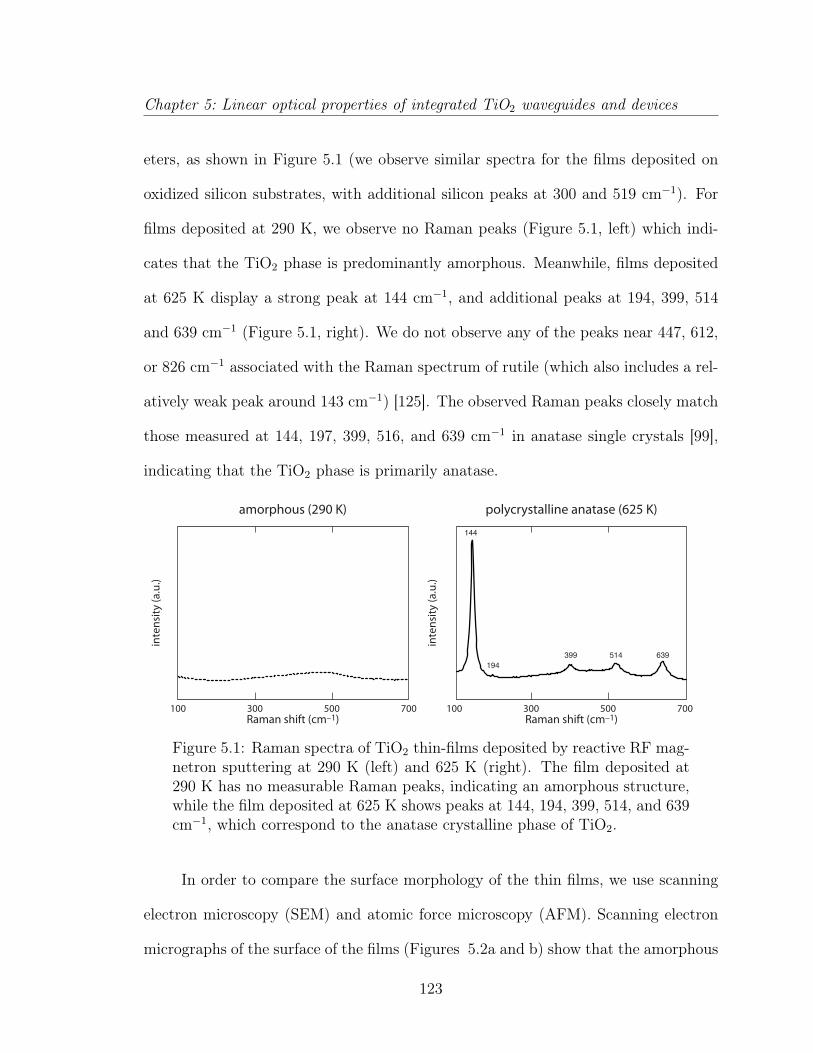
Chapter 5: Linear optical properties of integrated TiO2 waveguides and devices
eters, as shown in Figure 5.1 (we observe similar spectra for the films deposited on
oxidized silicon substrates, with additional silicon peaks at 300 and 519 cm−1). For
films deposited at 290 K, we observe no Raman peaks (Figure 5.1, left) which indi-
cates that the TiO2 phase is predominantly amorphous. Meanwhile, films deposited
at 625 K display a strong peak at 144 cm−1, and additional peaks at 194, 399, 514
and 639 cm−1 (Figure 5.1, right). We do not observe any of the peaks near 447, 612,
or 826 cm−1 associated with the Raman spectrum of rutile (which also includes a rel-
atively weak peak around 143 cm−1) [125]. The observed Raman peaks closely match
those measured at 144, 197, 399, 516, and 639 cm−1 in anatase single crystals [99],
indicating that the TiO2 phase is primarily anatase.
100 300 500 700
inte
nsity
(a.u
.)
144
399194
514 639
100 300 500 700Raman shift (cm–1)
inte
nsity
(a.u
.)
amorphous (290 K) polycrystalline anatase (625 K)
Raman shift (cm–1)
Figure 5.1: Raman spectra of TiO2 thin-films deposited by reactive RF mag-netron sputtering at 290 K (left) and 625 K (right). The film deposited at290 K has no measurable Raman peaks, indicating an amorphous structure,while the film deposited at 625 K shows peaks at 144, 194, 399, 514, and 639cm−1, which correspond to the anatase crystalline phase of TiO2.
In order to compare the surface morphology of the thin films, we use scanning
electron microscopy (SEM) and atomic force microscopy (AFM). Scanning electron
micrographs of the surface of the films (Figures 5.2a and b) show that the amorphous
123

Chapter 5: Linear optical properties of integrated TiO2 waveguides and devices
structure is granular, while the anatase film consists of densely packed nanocrystals.
AFM scanning images, obtained in non-contact alternating current mode with a 9-
nm-radius cantilever tip, reveal root mean square (RMS) roughness of 0.4 and 2.7 nm
for the amorphous and anatase films, respectively (Figures 5.2c and d).
100 nm100 nm
anatase (625 K)amorphous (290 K)a b
c d anatase (625 K)amorphous (290 K)
Figure 5.2: Surface morphology of TiO2 thin films: SEM images of (a) amor-phous and (b) polycrystalline anatase thin-film surfaces; and AFM surfacescans of (c) amorphous and (d) polycrystalline anatase thin-films showingRMS roughness of 0.4 and 2.7 nm, respectively.
We measure the optical properties of both TiO2 films in the visible and near-
infrared spectrum using a variable angle prism coupling system [98]. Table 5.2 summa-
rizes the refractive indices of the TiO2 films at 633, 826, 1310 and 1550 nm measured
using transverse-electric (TE) polarized light. Both films have refractive indices of
124

Chapter 5: Linear optical properties of integrated TiO2 waveguides and devices
Table 5.2: Refractive indices and propagation losses of TiO2 thin films. Thefilms are 0.25 µm thick, consisting of amorphous and polycrystalline anataseTiO2 on oxidized silicon substrates. Both indices and losses are determinedby prism coupling using TE-polarization. We estimate an uncertainty of±0.002 for the refractive index measurements and ±20% for the loss mea-surements.
Amorphous TiO2 Anatase TiO2
wavelength refractive propagation loss refractive Propagation loss(nm) index (dB/mm) index (dB/mm)633 2.426 0.12 2.486 > 2.0
826 2.372 0.06 2.427 2.01310 2.323 0.04 2.375 0.911550 2.315 0.04 2.366 0.42
around 2.4 at 826 nm, with the anatase film having a slightly higher refractive index.
Measurements using transverse-magnetic (TM) polarized light at 826 nm reveal a
slight birefringence for both films, the TM indices being 0.006 and 0.012 higher in
the amorphous and anatase films, respectively. Table 5.2 also shows the thin-film
propagation losses measured by scanning a fiber along the coupled planar waveguide
mode normal to the surface of the film. Using a germanium detector, we collect scat-
tered light versus position and fit the data to an exponential curve. The anatase films
exhibit losses ranging from > 2.0 dB/mm at 633 nm (beyond the measurable limit of
the prism coupling system) to 0.42 ±0.08 dB/mm at 1550 nm. The amorphous TiO2
thin-film propagation losses are significantly lower and are less wavelength-dependent,
varying from 0.12 ±0.02 dB/mm at 633 nm to 0.04 ±0.01 dB/mm at 1550 nm.
125

Chapter 5: Linear optical properties of integrated TiO2 waveguides and devices
5.1.3 Submicrometer-wide TiO2 waveguides
Waveguide fabrication
We apply standard top-down fabrication methods to define submicrometer-wide waveg-
uides in our amorphous and anatase TiO2 thin films. First, we expose the waveguide
pattern into a 300-nm-thick positive electron-beam (e-beam) resist layer (ZEP) on
top of the TiO2 film using a 100-keV electron-beam lithography system. The applied
e-beam parameters include a 300 × 300 µm write window, a beam current of 100
pA, and a dose of 400 µC/cm2. After developing the exposed resist, we deposit a
50-nm-thick chromium film by e-beam evaporation and perform metal lift-off to form
a metal etch mask. We then transfer the metal pattern into the TiO2 film using
electron cyclotron resonance reactive ion etching. The etch parameters include a CF4
and H2 gas mixture in a ratio of 4:1, a microwave power of 300 W, a substrate power
of 150 W, and a chamber pressure of 5 mTorr. Using surface profilometry, we find
that the etch rates of the amorphous and anatase films are approximately 50 and
60 nm/min, respectively. After etching, we remove the remaining metal mask using
Cr-etchant, and apply a 1.6-µm-thick fluoropolymer top-cladding layer (n = 1.39).
Finally, we cleave the chips to prepare waveguide end-facets.
Figures 5.3a and 5.3b show scanning electron micrographs of the resulting amor-
phous and anatase TiO2 waveguides (without top-cladding), respectively. Both types
of waveguides have relatively smooth, uniform sidewalls with slopes of approximately
75°. The cross-section of the anatase TiO2 waveguide facet reveals the TiO2 core to
consist of close-packed vertical nanocrystalline columns (Figure 5.3b).
126
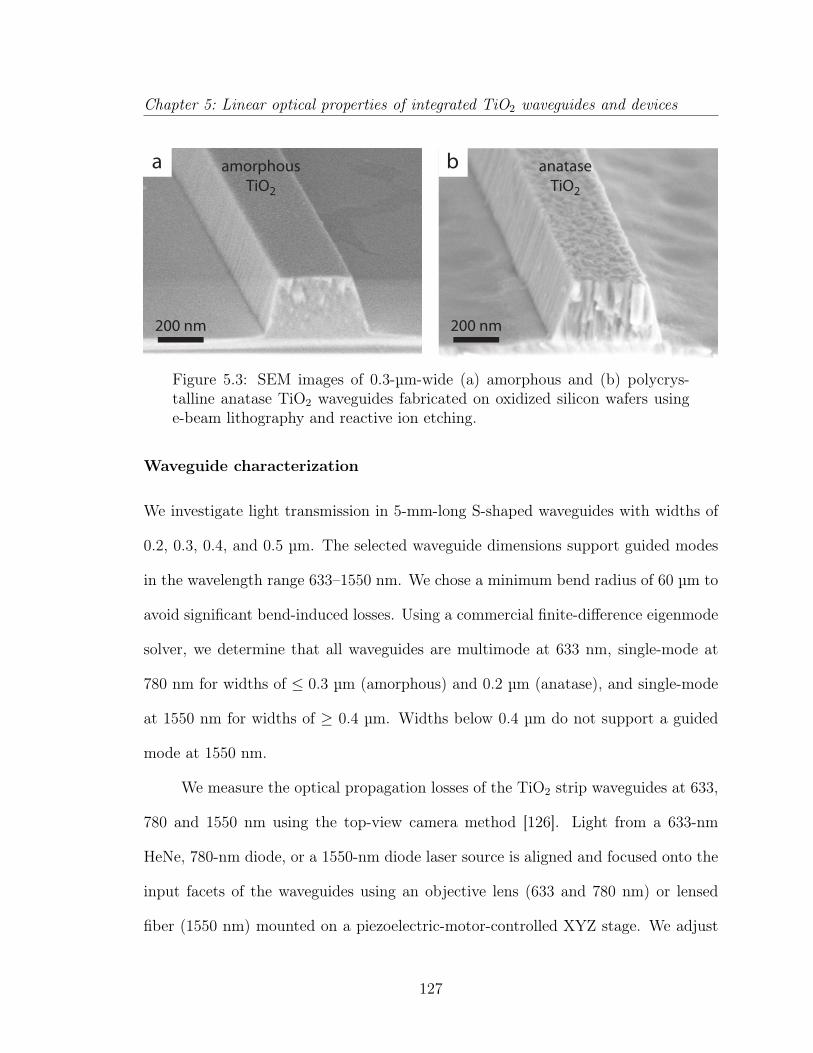
Chapter 5: Linear optical properties of integrated TiO2 waveguides and devices
200 nm200 nm
amorphousTiO2
anataseTiO2
a b
Figure 5.3: SEM images of 0.3-µm-wide (a) amorphous and (b) polycrys-talline anatase TiO2 waveguides fabricated on oxidized silicon wafers usinge-beam lithography and reactive ion etching.
Waveguide characterization
We investigate light transmission in 5-mm-long S-shaped waveguides with widths of
0.2, 0.3, 0.4, and 0.5 µm. The selected waveguide dimensions support guided modes
in the wavelength range 633–1550 nm. We chose a minimum bend radius of 60 µm to
avoid significant bend-induced losses. Using a commercial finite-difference eigenmode
solver, we determine that all waveguides are multimode at 633 nm, single-mode at
780 nm for widths of ≤ 0.3 µm (amorphous) and 0.2 µm (anatase), and single-mode
at 1550 nm for widths of ≥ 0.4 µm. Widths below 0.4 µm do not support a guided
mode at 1550 nm.
We measure the optical propagation losses of the TiO2 strip waveguides at 633,
780 and 1550 nm using the top-view camera method [126]. Light from a 633-nm
HeNe, 780-nm diode, or a 1550-nm diode laser source is aligned and focused onto the
input facets of the waveguides using an objective lens (633 and 780 nm) or lensed
fiber (1550 nm) mounted on a piezoelectric-motor-controlled XYZ stage. We adjust
127

Chapter 5: Linear optical properties of integrated TiO2 waveguides and devices
the polarization of the incident light using a half-wave plate and a polarizer prior to
the objective lens (633 and 780 nm) and a paddle-based polarization controller before
the lensed fiber (1550 nm). We capture images using microscope-mounted CMOS
(633 and 780 nm) and InGaAs (1550 nm) cameras and determine the transmission
through the TiO2 waveguides by analyzing the relative intensity of scattered light
along the waveguides in the resulting images.
In Figure 5.4 we show representative top-view camera images of visible and
infrared light propagation in our amorphous (Figures 5.4a, c and e) and polycrystalline
anatase (Figures 5.4b, d and f) waveguides. The propagation loss data corresponding
to the representative images is shown in Figures 5.5a and b. Table 5.3 summarizes the
propagation-loss data measured for different waveguide widths. The amorphous losses
are considerably lower than the anatase losses at 633 and 780 nm. The uncertainty in
the fit for the InGaAs camera measurements is rather high (±50%) due to the large
relative background intensities in the images. Therefore, we measure similar losses at
1550 nm in both types of TiO2 waveguide within the experimental uncertainty.
5.1.4 TiO2 microphotonic features
Design and fabrication of microphotonic features
As a proof of principle, we investigate microphotonic features at 780 nm, near TiO2’s
half-bandgap and where nonlinear optical devices are feasible in bulk rutile TiO2 [11].
We base our devices on a 0.3-µm-wide amorphous TiO2 waveguide, which supports a
single, well-confined TE-mode and has lower losses than similar anatase waveguides
around 800 nm. To investigate waveguide bending losses, we fabricate waveguides
128

Chapter 5: Linear optical properties of integrated TiO2 waveguides and devices
100 µm
anataseλ = 1550 nm
500 µm
anataseλ = 780 nm
500 µm
anataseλ = 633 nm
100 µm
amorphousλ = 1550 nm
500 µm
amorphousλ = 780 nm
500 µm
amorphousλ = 633 nm
a b
c d
fe
Figure 5.4: Top-view CMOS (633 nm and 780 nm) and InGaAs (1550 nm)camera images showing light propagation at different wavelengths λ in amor-phous and polycrystalline anatase TiO2 waveguides. The waveguides are0.2-µm wide (a–d) and 0.5-µm wide (e and f).
129
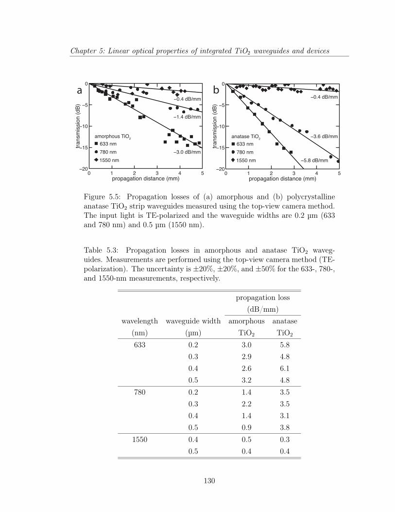
Chapter 5: Linear optical properties of integrated TiO2 waveguides and devices
−0.4 dB/mm
−3.6 dB/mm
−5.8 dB/mm
anatase TiO2
1550 nm
780 nm
633 nm
propagation distance (mm)
tran
smis
sion
(dB
)
0 1 2 3 4 5
0
−5
−10
−15
−20
amorphous TiO2
−0.4 dB/mm
−1.4 dB/mm
−3.0 dB/mm
1550 nm
780 nm
633 nm
propagation distance (mm)
tran
smis
sion
(dB
)
0 1 2 3 4 5
0
−5
−10
−15
−20
a b
Figure 5.5: Propagation losses of (a) amorphous and (b) polycrystallineanatase TiO2 strip waveguides measured using the top-view camera method.The input light is TE-polarized and the waveguide widths are 0.2 µm (633and 780 nm) and 0.5 µm (1550 nm).
Table 5.3: Propagation losses in amorphous and anatase TiO2 waveg-uides. Measurements are performed using the top-view camera method (TE-polarization). The uncertainty is ±20%, ±20%, and ±50% for the 633-, 780-,and 1550-nm measurements, respectively.
propagation loss(dB/mm)
wavelength waveguide width amorphous anatase(nm) (µm) TiO2 TiO2
633 0.2 3.0 5.80.3 2.9 4.80.4 2.6 6.10.5 3.2 4.8
780 0.2 1.4 3.50.3 2.2 3.50.4 1.4 3.10.5 0.9 3.8
1550 0.4 0.5 0.30.5 0.4 0.4
130

Chapter 5: Linear optical properties of integrated TiO2 waveguides and devices
with multiple bends having radii of 1–20 µm. In addition, we fabricate optical couplers
consisting of two waveguides with adiabatic sine-bends into and out of a parallel
coupling region. The spacing of the coupling region is 0.2 µm and its length, L, varies
from 0 to 4 µm. We measure the transmission characteristics of the bends and optical
couplers using the top-view camera method.
Micro-bends
Figure 5.6 summarizes the measurements and characterization of the TiO2 microbends.
Figure 5.6a shows the simulated electric field profile of the fundamental 780-nm TE
mode confined by the amorphous-TiO2 waveguide. In Figure 5.6b, we display a top-
view SEM image of a representative TiO2 waveguide with micro-bends having radii
r of 5 µm prior to cladding layer deposition. In Figure 5.6c, we show camera images
of light transmission through cladded micro-bend features with r = 20 µm (top), 10
µm (middle) and 5 µm (bottom). Figure 5.6d displays the measured transmission
for varying r. The plot shows a minimal change in transmission as r is decreased to
a value of 3 µm. At r = 2 µm we observe a change in transmission of −9 dB that
corresponds to an added loss of < 1 dB/90° bend. For r = 1 µm, the transmission is
below the measurable limit (−40 dB).
Optical-couplers
Figure 5.7a displays an SEM image of an optical-coupler (prior to cladding deposition)
with a parallel interaction length L = 4 µm. Figure 5.7b shows optical images of light
transmission in couplers with L = 0 µm (top), L = 2 µm (middle) and L = 4 µm
(bottom). By measuring the scattered intensity in each output branch of the coupler
131

Chapter 5: Linear optical properties of integrated TiO2 waveguides and devices
bend radius (μm)
tran
smis
sion
(dB
)
experimental data
simulated data
0 5 10 15 20
0
−5
−10
−15
−2050 µm
r = 20 µm
r = 10 µm
r = 5 µm
10 µm
r
0
0.2
0.4
0.6
0.8
1
500 nm
x
y
TE0 mode, Exλ = 780 nm
ba
dc
Figure 5.6: Calculated TE-like field profile of the fundamental 780-nm modein a straight 0.25 µm × 0.3 µm amorphous TiO2 waveguide; (b) SEM top-view image of a bend-transmission test-feature consisting of a 0.25 µm ×0.3 µm amorphous TiO2 waveguide with fourteen consecutive 90° bends witha radius r of 5 µm; (c) CMOS camera images showing light transmissionthrough test features with r = 20 µm (top), r = 10 µm (middle), and r = 5µm (bottom); (d) measured and simulated transmission for varying bendradii.
132

Chapter 5: Linear optical properties of integrated TiO2 waveguides and devices
(Iupper and Ilower) we determine splitting ratios Iupper/(Iupper + Ilower) of 0.3, 0.6, and
0.9, respectively.
50 µm
L = 4 µm
L = 2 µm
L = 0 µm
10 µm
L
ba
Figure 5.7: TiO2 microphotonic couplers: (a) SEM image of a TiO2 optical-coupler with adiabatic input/output transitions and a parallel interactionregion with a waveguide spacing of 0.2 µm and length, L, of 4 µm; (b) CMOSimages showing splitting ratios (light transferred to the upper waveguidedivided by the total transmitted intensity) of 0.3 (top), 0.6 (middle), and 0.9(bottom) for L = 0, 2 and 4 µm, respectively (780-nm light, TE polarization).
5.1.5 Discussion
We show that by adjusting substrate temperature, oxygen flow rate and RF sputtering
power, we can deposit waveguide-quality amorphous and polycrystalline-anatase TiO2
thin films. At visible and near-infrared wavelengths, our amorphous TiO2 thin films
exhibit significantly lower propagation losses. The difference in propagation loss is
most evident in the visible. In the 0.25-µm-thick films prepared for this study, we
observe a pronounced visible streak of light across tens of mm in the amorphous
film, but observe no measureable 633-nm-light propagation in the polycrystalline
film. We partially attribute the difference in loss to the larger surface roughness
in the anatase thin film. Despite having higher thin-film losses, the anatase phase
133

Chapter 5: Linear optical properties of integrated TiO2 waveguides and devices
of TiO2 offers potential advantages for microphotonic devices in terms of greater
thermal stability [127], higher refractive index, and higher nonlinearity [53]. Reduced
nanocrystal size and smoother surfaces may lead to lower losses in the polycrystalline
films.
We also demonstrate a suitable method for fabricating submicrometer-wide strip
waveguides using both types of TiO2 thin film. The amorphous TiO2 strip waveguides
have lower propagation losses at 633 and 780 nm than the anatase waveguides. As
with the thin films, the difference is most significant at 633 nm, where we have recently
demonstrated amorphous TiO2 microring resonators for visible-light systems [121]. In
both amorphous and polycrystalline waveguides, we measure losses on the order of
0.3–.5 dB/mm at 1550 nm, which are comparable to those initially reported in other
high-refractive-index-contrast photonic waveguides [94, 102, 128]. The comparable
losses at 1550 nm can be explained by the reduced influence of surface and edge
roughness, and the low optical confinement within the TiO2 core (< 40%) whereby
the majority of light propagates in the low-loss cladding layers.
The measured strip-waveguide propagation losses are sufficiently low for mi-
crophotonic devices requiring µm and mm waveguide lengths. However, we observe
significantly higher propagation losses in our TiO2 strip waveguides compared to
the unstructured planar films, as is typical in high-refractive-index-contrast waveg-
uides [129]. Moreover, the waveguide losses exhibit greater wavelength dependence
than the thin film losses based on the relative values measured at 633 and 1550
nm. Several mechanisms may introduce additional losses in our strip waveguides,
including radiation of higher-order modes, scattering due to core-cladding interfacial
134

Chapter 5: Linear optical properties of integrated TiO2 waveguides and devices
roughness, and e-beam write-field stitching errors [129, 130]. Each loss mechanism
theoretically scales inversely with wavelength, consistent with observation. We may
reduce waveguide losses towards the thin-film values using alternative waveguide ge-
ometries [131], complimentary fabrication methods [132], or specialized e-beam writ-
ing strategies [133].
By investigating amorphous TiO2 microphotonic features, we show that light is
transmitted through waveguide bends with radii down to 2 µm and demonstrate TiO2
optical couplers. To gain insight into the loss mechanisms of the investigated bend
structures, we compare the simulated transmission properties of TiO2 microphotonic
bends with our experimental results. In Figure 5.6d we show the calculated trans-
mission through micro-bends as a function of bend radius. The total calculated loss
includes the losses due to modal overlap mismatch at the interface between straight
and bent waveguides and between 90°-bends of opposite direction, radiation losses
from the 90°-bends, and the experimental propagation loss of 2 ± 0.4 dB/mm mea-
sured in 300-nm-wide amorphous TiO2 waveguides. We observe a good agreement
between the calculated and experimental data. In the calculated data, the primary
contribution to the total loss is the modal overlap mismatch at the interfaces, and
not radiative loss due to the bend itself. For example, we calculate a bend-bend
transition loss of 0.75 dB compared with a radiation loss of 0.01 dB for a 90° bend
with r = 2 µm. For micro-bends with r ≤ 2 µm, the transmission can be improved by
incorporating adiabatic transitions. We also expect that comparably small bend radii
are feasible in anatase waveguides due to their similar dimensions and refractive in-
dices. These results, combined with the high optical confinement in TiO2 waveguides,
135
Chapter 5: Linear optical properties of integrated TiO2 waveguides and devices
demonstrate that TiO2 devices can be densely integrated on photonic chips.
To compare our optical-coupler measurements to the theoretical splitting ratios,
we calculate the coupling distance by solving for the even and odd TE-polarized
modes in the investigated structures. We calculate effective indices of 1.919 and
1.885, respectively, for which coupled-mode theory predicts a 100% coupling length
of 12 µm. This value is consistent with the experimentally observed coupling ratios
and lengths when we account for the additional effective coupling length introduced
by the adiabatic input and output regions (6 µm). We measure a splitting-ratio of
approximately 90% for an effective length of 10 µm. Our data shows that we can
achieve strong coupling over short lengths, allowing for small footprints for devices
such as ring resonators.
5.1.6 Conclusion
In conclusion, we have fabricated amorphous and polycrystalline anatase TiO2 thin
films and strip waveguides with submicrometer widths. We observe light propagation
over mm-length scales at 633 and 780 nm, and measure losses of 0.4 ± 0.2 dB/mm
in amorphous and anatase strip-waveguides at 1550 nm. The consistency between
simulated and experimental micro-bend and optical-coupler results suggest that real-
izing complex micro-scale TiO2 photonic devices can be achieved using the techniques
reported here. These results demonstrate TiO2 to be a novel and promising platform
for visible to infrared microphotonic devices.
136

Chapter 5: Linear optical properties of integrated TiO2 waveguides and devices
Acknowledgements
Several people contributed to the work described in this paper. All authors provided
contributions to the basic ideas described in this work. JDBB, CCE., JTC, OR,
PBD, FP, and KCP designed and carried out the experiments, and analyzed the re-
sults. ML and EM supervised the research and the development of the manuscript.
JDBB. wrote the first draft of the manuscript; all authors subsequently took part in
the revision process and approved the final copy of the manuscript. Rafael Gattass
and Ruwan Senaratne contributed to the preliminary research and Laura Tucker and
Phillip Munoz provided feedback on the manuscript throughout its development. The
devices were fabricated at the Center for Nanoscale Systems at Harvard University.
The research described in this paper was supported by the National Science Foun-
dation under contract ECCS-0901469, the Harvard Quantum Optics Center, and the
Fonds de recherche du Québec - Nature et technologies. JTC and PBD were partially
supported by the Center for Excitonics, an Energy Frontier Research Center funded
by the U.S. Department of Energy, Office of Science, Office of Basic Energy Sciences
under Award Number DE-SC0001088.
5.2 Racetrack resonators for visible photonics
The following paper appears in Optics Letters 37 (4), 539-541, 2012.
137
Chapter 5: Linear optical properties of integrated TiO2 waveguides and devices
Integrated TiO2 resonators for visible photonics
J. T. Choy, J. D. B. Bradley, P. B. Deotare, I. B. Burgess, C. C. Evans, E. Mazur,
and M. Lončar
School of Engineering and Applied Sciences, Harvard University,
9 Oxford Street, Cambridge, Massachusetts 02138, USA
Abstract: We demonstrate waveguide-coupled titanium dioxide (TiO2) racetrack res-
onators with loaded quality factors of 2.2 × 10⁴ for the visible wavelengths. The
structures were fabricated in sputtered TiO2 thin films on oxidized silicon substrates
using standard top-down nanofabrication techniques, and passively probed in trans-
mission measurements using a tunable red laser.
Optical microresonators are ubiquitous components in optical telecommunica-
tion systems and provide a compact means for studying cavity quantum electro-
dynamics [134]. The integration of microresonators into classical and quantum net-
works relies on materials that support high-quality optical components on a chip-scale
[135,136]. In the growing field of quantum photonics, quantum emitters [137–139] op-
erate primarily in the visible wavelengths. Therefore, the development of a chip-scale
platform for the visible is a critical step toward the realization of quantum communica-
tion networks, and can be beneficial to classical applications, such as light generation
and on-chip sensing. While gallium phosphide [140], silicon nitride [136, 141, 142],
silicon dioxide [143], and diamond [144] are all promising materials, certain chal-
lenges remain, including intrinsic luminescence [141], difficulty of generating thin
membranes with low optical loss [145], poor refractive index contrast with the sur-
138

Chapter 5: Linear optical properties of integrated TiO2 waveguides and devices
rounding medium [143], and low tolerance for fabrication imperfections due to inher-
ently small characteristic lengths.
Titanium dioxide (TiO2) can be added to the family of viable integrated visible
photonics platforms. It is a widebandgap semiconductor (with a bandgap energy
between 3 –3.5 eV, depending on the crystalline phase [146]) with a moderately high
index for the visible wavelengths (n ≈ 2.4) and a wide transparency window from
the near UV to the IR. It is also naturally abundant and is compatible with a host
of conventional growth techniques. While the optical properties of TiO2 have been
exploited in three-dimensional photonic crystals [147], gratings [117], and waveguides
[119, 148], planar resonator structures in this material had yet to be demonstrated.
Here we show scalable and integrable TiO2 racetrack resonators, having loaded quality
factors (Q) of the order of 104 with efficient coupling to a feeding waveguide.
Amorphous TiO2 thin films of thickness 170 nm have been deposited on oxidized
silicon substrates using RF sputtering of a Ti target in an O2/Ar environment [148].
Prism coupling experiments [148] indicated that the deposited films have propagation
losses as low as 2 dB/cm. These losses suggest that the material-limited Q for optical
cavities is around 5 × 10⁵. We used racetrack resonators since they allow for con-
trollable coupling to a waveguide via the coupling length. The fabricated parameters
were designed to minimize bending losses (by making bending radii R = 30 µm). Ad-
ditionally, the waveguide-resonator separation g and coupling length L were chosen to
ensure efficient transfer of light signal between the cavity and waveguide. To optimize
the coupling, we set g = 130 nm and waveguide width w = 250 nm, and calculated
the coupling efficiency as a function of L, using the difference between the effective
139

Chapter 5: Linear optical properties of integrated TiO2 waveguides and devices
indices of the even (ne) and odd (no) eigenmodes of the coupled structure [149]. For
the range of wavelengths between 630 and 640 nm, L = 15 µm provides near critical
coupling for transverse electric (TE) polarized light.
We realized the designed structures using conventional top-down fabrication
techniques, which include electron beam lithography on a positive electron beam
resist (ZEP 520A), electron beam evaporation and liftoff of a chromium mask layer,
and reactive ion etching in a CF4/H2 environment. The recipe has an etch rate of
approximately 60 nm/min and leads to slightly slanted sidewalls with an angle of
75° [148]. The mask was subsequently removed by an etchant and polymer pads
(SU-8 2002, with cross sections 3 µm × 3 µm) were written using electron beam
lithography [150]. These pads overlap with the ends of the TiO2 waveguides and
extend to the edges of the chip (Figure 5.8 a). The edges of the polymer waveguides
were then cleaved to facilitate in- and out-coupling of light. The input and output
facets are offset from one another to avoid direct scattering of uncoupled light into
the collection fiber. The devices have surfaces with a roughness of around 10 nm and
gaps of approximately 130 nm in the coupling regions Figure 5.8 b–d).
We simulated the mode profiles of the fabricated devices (insets of Figure 5.8
b) using the finite element method (FEM). From Figure 5.8, the waveguides have an
etch depth of 150 nm and a width of 250 nm on their top facets. These dimensions
support one fundamental mode in each of the TE and transverse magnetic (TM)
polarizations with respective effective indices of 1.80 and 1.61 at a wavelength of 630
nm. The pedestal layer, which resulted from non-uniformity in our etching process,
is roughly 20 nm thick and can be beneficial for waveguide-resonator coupling [136].
140

Chapter 5: Linear optical properties of integrated TiO2 waveguides and devices
Figure 5.8: (a) Optical image of a set of TiO2 waveguide-racetrack devicesintegrated with polymer pads. Inset: overlapping region between the TiO2
waveguide and polymer pad. SEM images of (b) a TiO2 waveguide-resonator,(c) its coupling region, and (d) etch profile taken at a 45° tilt. Insets: crosssections of the fabricated waveguide-resonator with simulated electric fieldprofiles of the TE (top) and TM (bottom) modes. Propagation is in the xdirection. Scalebar = 200 nm.
141

Chapter 5: Linear optical properties of integrated TiO2 waveguides and devices
In our structure, this layer improves coupling into the TM-polarized modes, so that
the simulated coupling efficiencies are around 90% for both TE- and TM-polarized
light.
The resonators were characterized by transmission measurements using a tun-
able red laser with a scanning range of 634.4–639.6 nm. The output of the laser was
coupled to a single mode, tapered lens fiber that was rotated such that the input
signal into the sample was polarized along either the TE or TM direction. Light with
a spot size of 0.8 µm in diameter was focused onto the facet of the polymer pad by the
tapered lens fiber and transmitted into the waveguide-resonator device. The output
was coupled through a polymer pad on the opposite end of the chip and collected by
another tapered lens fiber that was connected to a high-speed silicon detector. For
this experiment, the coupling loss from the fiber to the TiO2 waveguide is roughly
14.5 dB at each end. This loss can be reduced by polishing the facets and optimizing
the geometry of the TiO2 waveguide to reduce light reflections that arise from the
refractive index mismatch.
The resonator transmission spectra are shown in Figure 5.9. All spectra shown
here have not been normalized. The transmission spectra have periodically spaced
dips corresponding to whispering gallery modes with either the TE (Figure 5.9 a)
or TM (Figure 5.9 b) polarization. The small dips observed in (Figure 5.9 b) are
due to imperfect polarization filtering of TE-polarized signals. The loaded quality
factors (Qloaded = λ/∆λ, where λ is the cavity resonance wavelength and ∆λ is the
linewidth of the resonance) were extracted by fitting the transmission dips to the Fano
model [151]. The model is necessary due to interference between the transmitted sig-
142
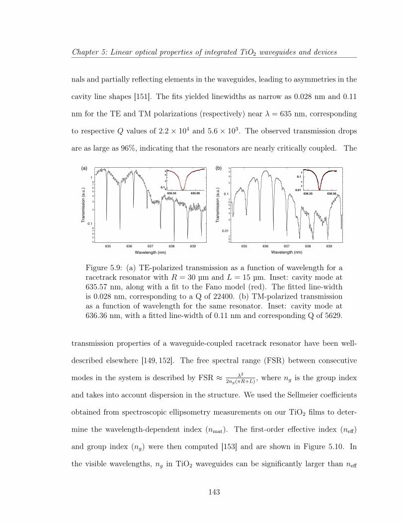
Chapter 5: Linear optical properties of integrated TiO2 waveguides and devices
nals and partially reflecting elements in the waveguides, leading to asymmetries in the
cavity line shapes [151]. The fits yielded linewidths as narrow as 0.028 nm and 0.11
nm for the TE and TM polarizations (respectively) near λ = 635 nm, corresponding
to respective Q values of 2.2 × 10⁴ and 5.6 × 10³. The observed transmission drops
are as large as 96%, indicating that the resonators are nearly critically coupled. The
4
5
678
0.1
2
3
4
5
678
1
Tra
nsm
issi
on (
a.u.
)
639638637636635
Wavelength (nm)
80.1
2
4
6
635.60635.55
(a)
567
0.01
2
3
4
567
0.1
2
3
4
5
Tra
nsm
issi
on (
a.u.
)
639638637636635
Wavelength (nm)
0.01
2
4
0.1
2
636.50636.25
(b)
Figure 5.9: (a) TE-polarized transmission as a function of wavelength for aracetrack resonator with R = 30 µm and L = 15 µm. Inset: cavity mode at635.57 nm, along with a fit to the Fano model (red). The fitted line-widthis 0.028 nm, corresponding to a Q of 22400. (b) TM-polarized transmissionas a function of wavelength for the same resonator. Inset: cavity mode at636.36 nm, with a fitted line-width of 0.11 nm and corresponding Q of 5629.
transmission properties of a waveguide-coupled racetrack resonator have been well-
described elsewhere [149, 152]. The free spectral range (FSR) between consecutive
modes in the system is described by FSR ≈ λ2
2ng(πR+L), where ng is the group index
and takes into account dispersion in the structure. We used the Sellmeier coefficients
obtained from spectroscopic ellipsometry measurements on our TiO2 films to deter-
mine the wavelength-dependent index (nmat). The first-order effective index (neff)
and group index (ng) were then computed [153] and are shown in Figure 5.10. In
the visible wavelengths, ng in TiO2 waveguides can be significantly larger than neff
143
Chapter 5: Linear optical properties of integrated TiO2 waveguides and devices
(a difference of approximately 57% for the TE mode and 70% for the TM mode).
The greater difference observed in the TM polarization is due to larger waveguide
dispersion, which can be estimated by calculation of the group index ng,w of the given
waveguide without considering the wavelength-dependence in nmat. The large dis-
crepancy between ng and neff can thus be attributed to both waveguide and material
dispersion, although the contribution from the latter decreases with increasing wave-
lengths, as indicated by the diminishing difference between the group index with and
without material dispersion (ng and ng,w, respectively). Dispersion must therefore be
considered when designing optical components in TiO2 and can be exploited to gen-
erate small FSRs without significantly increasing the device footprint. The calculated
ng values are in good agreement with the experimentally obtained value, in which an
FSR of 0.64 nm (Figure 5.9 a) corresponds to a group index of 2.92 in the 635 to 640
nm range in the TE polarization.
Finally, the propagation loss in a critically coupled resonator can be estimated
using αr = πngλQloaded
[154]. Based on a TE-polarized mode with a Q of 22400 and
transmission drop of 92% (inset of Figure 5.9 a), the corresponding propagation loss
is 28 dB/cm. The deviation from the planar loss value can be attributed to scattering
losses from surface roughness introduced by the fabrication process, which might be
reduced by using a top-cladding material.
We have demonstrated planar resonators in TiO2 thin films for visible light
operation with efficient coupling to waveguides for delivering light on- and off-chip.
The methods and devices shown here could help advance the TiO2 material platform
toward integration with active emitters for novel and integrated classical and non-
144
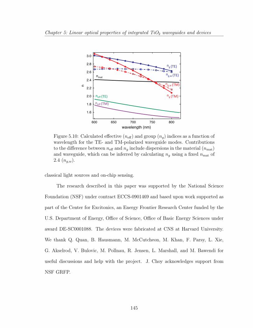
Chapter 5: Linear optical properties of integrated TiO2 waveguides and devices
3.0
2.8
2.6
2.4
2.2
2.0
1.8
1.6
n
800750700650600
wavelength (nm)
Figure 5.10: Calculated effective (neff) and group (ng) indices as a function ofwavelength for the TE- and TM-polarized waveguide modes. Contributionsto the difference between neff and ng include dispersions in the material (nmat)and waveguide, which can be inferred by calculating ng using a fixed nmat of2.4 (ng,w).
classical light sources and on-chip sensing.
The research described in this paper was supported by the National Science
Foundation (NSF) under contract ECCS-0901469 and based upon work supported as
part of the Center for Excitonics, an Energy Frontier Research Center funded by the
U.S. Department of Energy, Office of Science, Office of Basic Energy Sciences under
award DE-SC0001088. The devices were fabricated at CNS at Harvard University.
We thank Q. Quan, B. Hausmann, M. McCutcheon, M. Khan, F. Parsy, L. Xie,
G. Akselrod, V. Bulovic, M. Pollnau, R. Jensen, L. Marshall, and M. Bawendi for
useful discussions and help with the project. J. Choy acknowledges support from
NSF GRFP.
145

Chapter 6
Nonlinear properties of TiO2
waveguides
In this chapter, we present two studies on the nonlinear optical properties of inte-
grated polycrystalline-anatase TiO2 waveguides. The first paper describe spectral
broadening of femtosecond pulses which allows us to quantify nonlinear refraction,
multiphoton absorption, and stimulated Raman scattering. In the following section,
we present a preliminary results on third-harmonic generation in similar waveguides.
These simple wavelength conversion devices demonstrate TiO2’s potential for more
complex integrated nonlinear devices.
6.1 Spectral broadening
The following paper in appears in Optics Express 21 (15), 18582-18591, 2013.
146
Chapter 6: Nonlinear properties of TiO2 waveguides
Spectral broadening in anatase titanium dioxide
waveguides at telecommunication and near-visible
wavelengths
C. C. Evans,1 K. Shtyrkova,2 J. D. B. Bradley,1,2 O. Reshef,1
E. Ippen,2 and E. Mazur1
1School of Engineering and Applied Sciences, Harvard University,
9 Oxford Street, Cambridge, Massachusetts 02138, USA
2Department of Electrical Engineering and Computer Science, Massachusetts Institute of
Technology, 77 Massachusetts Avenue, Cambridge, Massachusetts 02139, USA
Abstract: We observe spectral broadening of femtosecond pulses in single-mode
anatase-titanium dioxide (TiO2) waveguides at telecommunication and near-visible
wavelengths (1565 and 794 nm). By fitting our data to nonlinear pulse propagation
simulations, we quantify nonlinear optical parameters around 1565 nm. Our fitting
yields a nonlinear refractive index of 0.16× 10⁻¹⁸ m2/W, no two-photon absorption,
and stimulated Raman scattering from the 144 cm−1 Raman line of anatase with a
gain coefficient of 6.6× 10⁻¹² m/W. Additionally, we report on asymmetric spectral
broadening around 794 nm. The wide wavelength applicability and negligible two-
photon absorption of TiO2 make it a promising material for integrated photonics.
6.1.1 Introduction
Integrated nonlinear optical devices have enabled many applications for traditional
telecommunication wavelengths (1300–1600 nm), ranging from all-optical switches,
147

Chapter 6: Nonlinear properties of TiO2 waveguides
wavelength converters, amplifiers and lasers, to applications in metrology and quan-
tum information [66, 89, 103, 155–161]. However, few materials are optimal for the
unique features of the near-visible window (NVIS, 800–1300 nm). Devices with
NVIS compatibility could link and process signals between different communications
bands throughout the full communications octave (800–1600 nm) and exploit efficient
sources for optical interconnects [162,163]. Additionally, such devices would open up
applications in biology (exploiting the low water absorption in the NVIS) [164–167]
and integrated quantum optics (utilizing inexpensive, high-performance silicon single-
photon detectors) [168]. Despite their promise, nonlinear optical applications for
NVIS wavelengths are almost completely unexplored due to insufficient integrated
materials.
Material properties dictate the operating wavelength for optimal performance
in all-optical devices. An ideal nonlinear optical material will achieve a maximum
effective nonlinearity while minimizing two-photon absorption (2PA) and have a high
refractive index to enable strong dispersion engineering for all wavelengths of interest.
The nonlinear index of refraction (n2) depends on the bandgap energy (Eg) and
scales as E−4g , strongly favoring narrow-bandgap materials [10,52,169]. This bandgap-
dependence explains silicon’s high nonlinearity (Eg = 1.1 eV, n2 = 4–6×10⁻¹⁸ m2/W
[170, 171]). However, strong 2PA in silicon at telecommunication wavelengths limits
many all-optical devices [27, 92]. Many materials such as chalcogenide glass [108],
AlGaAs [172,173] and GaInP [174] have excellent nonlinear optical properties for the
1300–1600 nm telecommunication band, yet are limited by 2PA in the NVIS window.
For maximum performance at a given operating wavelength, the scaling rules suggest
148
Chapter 6: Nonlinear properties of TiO2 waveguides
avoiding this limit by selecting a material with bandgap energy of slightly more than
twice the single-photon energy. Using these guidelines, we should achieve maximum
performance in the NVIS window using a material with a bandgap energy of 3.1 eV.
Titanium dioxide’s (TiO2) unique balance of large optical nonlinearity and wide
wavelength compatibility makes it optimal for NVIS operation. TiO2 exists in several
crystalline phases including rutile (Eg = 3.1 eV), anatase (Eg = 3.2 eV), and brookite
(Eg = 3.1 eV) making it ideal for wavelengths near 800 nm [47, 48]. The nonlinear
index of bulk and thin-film TiO2 typically ranges from 0.8–3 ×10⁻¹⁸ m2/W in the
NVIS window [11, 44, 54, 57, 60], which is an order of magnitude greater than the
nonlinear index of silica fiber (2.48 × 10⁻²⁰ m2/W [21]). However, values obtained
from thin-films measurements have been reported as large as 5 × 10⁻¹⁷ m2/W [59],
and as small as 1 × 10⁻¹⁹ m2/W [61] and −6 × 10⁻¹⁷ m2/W [53]. Although there
are no reported nonlinearity measurements of bulk anatase, for thin films the value
of n2 for anatase is very similar to that for rutile [53, 54]. The visible transparency
and minimal 2PA near 800 nm make TiO2 most comparable to silicon nitride [103].
However, TiO2 has a reported Kerr nonlinearity that is over three-times greater than
silicon nitride, it possesses a greater refractive index (2.4 versus 2.0), and it can be
deposited at low temperatures (< 400 C), allowing for back-end integration with
silicon microphotonic devices [11,121,148]. Even though TiO2 is well suited for NVIS
applications, integrated nonlinear optical devices in TiO2 remain undeveloped and
unexplored.
In this study, we demonstrate and characterize nonlinear pulse propagation in
recently developed anatase TiO2 waveguides [148]. We observe nonlinear spectral
149
Chapter 6: Nonlinear properties of TiO2 waveguides
broadening of femtosecond pulses with central wavelengths (λ0) of 1565 and 794
nm, spanning the communications octave. We fit our measurements to simulations
to quantify nonlinear optical parameters and we discuss potential applications for
this new material platform. This study represents the first demonstration of optical
nonlinearities in integrated TiO2 devices.
6.1.2 Experimental Procedure
We investigate waveguides of various dimensions to ensure strongly confined single-
mode operation at widely spaced wavelengths. We fabricate polycrystalline anatase
strip-waveguides on silicon substrates with SiO2 lower cladding and fluoropolymer
top cladding using previously reported methods [148]. The waveguides reported here
are 250-nm high, have top-widths of 900 and 200 nm, and are 9 and 6 mm long
for measurements at 1565 and 794 nm, respectively. Figure 6.1(a) shows a typical
cross section of a polycrystalline anatase waveguide before applying the top cladding,
making evident both the polycrystallinity of the anatase material and the 75 side-
wall angle. Figures 1(b) and 1(c), show simulated optical intensity profiles for the
waveguides (at 1565 nm and 794 nm, respectively). Our fabricated waveguides are
single-mode and strongly confine the light at each wavelength of interest, facilitating
measurement and parameter extraction.
We observe nonlinear pulse propagation by comparing the input versus output
spectra of pulses propagating within our waveguides as a function of the input pulse
energy. Our measurements are taken with two laser systems: an optical parametric
oscillator tuned to 1565 nm and a Ti:Sapphire oscillator centered at 794 nm. We
150
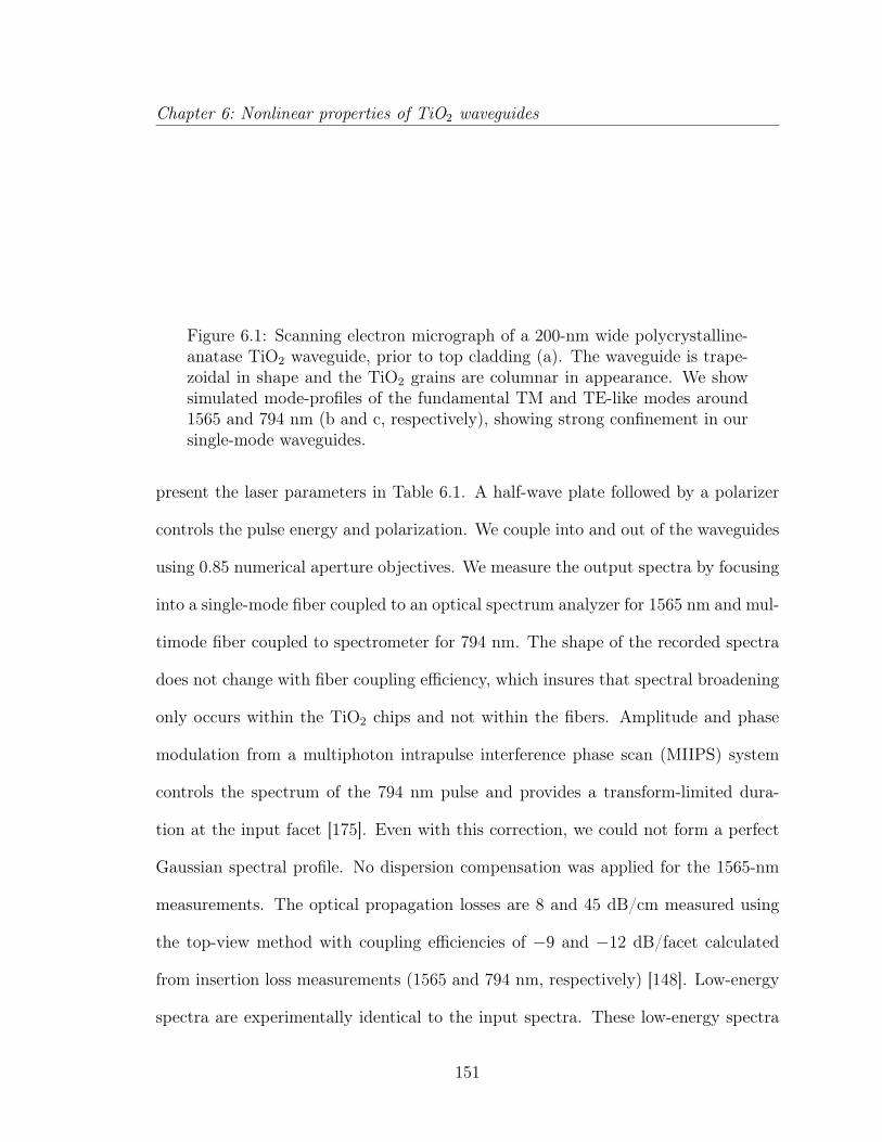
Chapter 6: Nonlinear properties of TiO2 waveguides
λ = 794 nm
0
1
λ = 1565 nm400 nm
TiO2
SiO2
a b c
Figure 6.1: Scanning electron micrograph of a 200-nm wide polycrystalline-anatase TiO2 waveguide, prior to top cladding (a). The waveguide is trape-zoidal in shape and the TiO2 grains are columnar in appearance. We showsimulated mode-profiles of the fundamental TM and TE-like modes around1565 and 794 nm (b and c, respectively), showing strong confinement in oursingle-mode waveguides.
present the laser parameters in Table 6.1. A half-wave plate followed by a polarizer
controls the pulse energy and polarization. We couple into and out of the waveguides
using 0.85 numerical aperture objectives. We measure the output spectra by focusing
into a single-mode fiber coupled to an optical spectrum analyzer for 1565 nm and mul-
timode fiber coupled to spectrometer for 794 nm. The shape of the recorded spectra
does not change with fiber coupling efficiency, which insures that spectral broadening
only occurs within the TiO2 chips and not within the fibers. Amplitude and phase
modulation from a multiphoton intrapulse interference phase scan (MIIPS) system
controls the spectrum of the 794 nm pulse and provides a transform-limited dura-
tion at the input facet [175]. Even with this correction, we could not form a perfect
Gaussian spectral profile. No dispersion compensation was applied for the 1565-nm
measurements. The optical propagation losses are 8 and 45 dB/cm measured using
the top-view method with coupling efficiencies of −9 and −12 dB/facet calculated
from insertion loss measurements (1565 and 794 nm, respectively) [148]. Low-energy
spectra are experimentally identical to the input spectra. These low-energy spectra
151
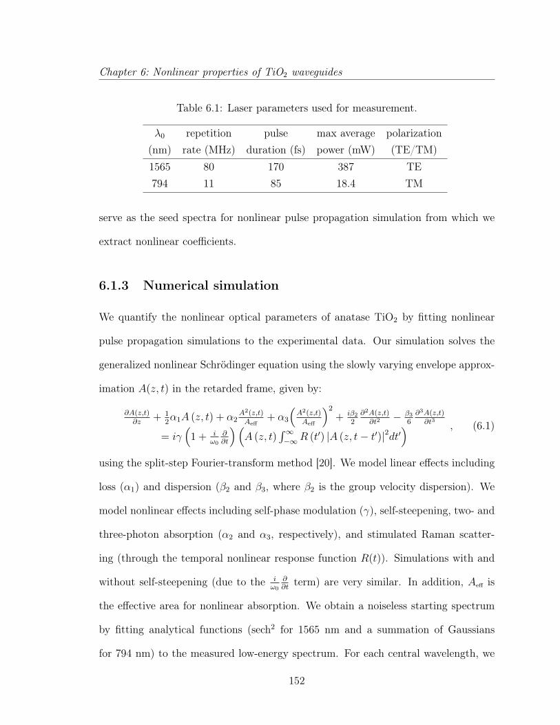
Chapter 6: Nonlinear properties of TiO2 waveguides
Table 6.1: Laser parameters used for measurement.
λ0 repetition pulse max average polarization(nm) rate (MHz) duration (fs) power (mW) (TE/TM)1565 80 170 387 TE794 11 85 18.4 TM
serve as the seed spectra for nonlinear pulse propagation simulation from which we
extract nonlinear coefficients.
6.1.3 Numerical simulation
We quantify the nonlinear optical parameters of anatase TiO2 by fitting nonlinear
pulse propagation simulations to the experimental data. Our simulation solves the
generalized nonlinear Schrödinger equation using the slowly varying envelope approx-
imation A(z, t) in the retarded frame, given by:
∂A(z,t)∂z
+ 12α1A (z, t) + α2
A2(z,t)Aeff
+ α3
(A2(z,t)Aeff
)2
+ iβ2
2∂2A(z,t)∂t2
− β3
6∂3A(z,t)∂t3
= iγ(
1 + iω0
∂∂t
)(A (z, t)
∫∞−∞R (t′) |A (z, t− t′)|2dt′
) , (6.1)
using the split-step Fourier-transform method [20]. We model linear effects including
loss (α1) and dispersion (β2 and β3, where β2 is the group velocity dispersion). We
model nonlinear effects including self-phase modulation (γ), self-steepening, two- and
three-photon absorption (α2 and α3, respectively), and stimulated Raman scatter-
ing (through the temporal nonlinear response function R(t)). Simulations with and
without self-steepening (due to the iω0
∂∂t
term) are very similar. In addition, Aeff is
the effective area for nonlinear absorption. We obtain a noiseless starting spectrum
by fitting analytical functions (sech2 for 1565 nm and a summation of Gaussians
for 794 nm) to the measured low-energy spectrum. For each central wavelength, we
152

Chapter 6: Nonlinear properties of TiO2 waveguides
calculate linear waveguide parameters that determine light-matter interactions such
as the effective area and chromatic dispersion. We extract the nonlinear coefficients
by minimizing the mean squared error between simulated and measured data while
leaving linear parameters fixed. The values extracted represent a single model that
applies to all of the measured data at one wavelength.
Simulating the mode structure of the waveguides allows us to calculate the num-
ber of modes and linear waveguide parameters. We determine the energy distribu-
tions, F (x, y), and propagation constants within the waveguide (shown in Figs. 1(b)
and 1(c), 1565 and 794 nm, respectively) using a finite-difference eigenmode solver.
The 900-nm waveguide only supports a TE mode for λ0 = 1565 nm and the 200-nm
waveguide supports fundamental TE-like and TM-like modes for λ0 = 794 nm, sim-
plifying pulse propagation simulation. Having identified the number and distributions
of the modes, we calculate the effective nonlinearity and chromatic dispersion.
The strength of the nonlinear interaction is given by the effective nonlinearity
γ, which we calculate from the energy distribution using [20]:
γ =2π
λ
∫ ∫∞−∞ n2 (x, y) |F (x, y)|4dxdy(∫ ∫∞
−∞ |F (x, y)|2dxdy)2 . (6.2)
Using n2 = 3 × 10⁻²⁰ m2/W for both silica and the fluoropolymer top cladding and
γ determined during fitting, we solve this equation for n2 in the TiO2 core. The
nonlinearity attributed to the cladding is 10 % for 1565 nm and less than 1 % for 794
nm. Assuming no nonlinear absorption in the cladding, we use a similar expression
to calculate effective nonlinear absorption areas, Aeff, of 0.43 and 0.16 µm2 for 1565
nm and 794 nm, respectively [20].
Our model includes the waveguide’s group velocity dispersion (GVD), which
153
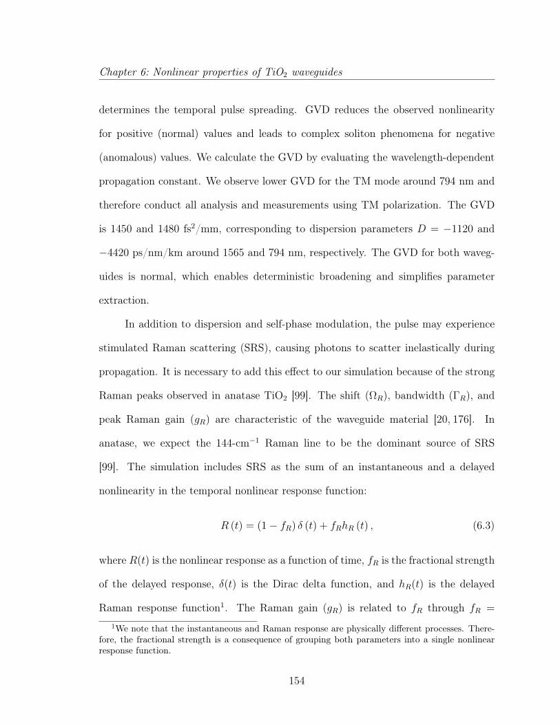
Chapter 6: Nonlinear properties of TiO2 waveguides
determines the temporal pulse spreading. GVD reduces the observed nonlinearity
for positive (normal) values and leads to complex soliton phenomena for negative
(anomalous) values. We calculate the GVD by evaluating the wavelength-dependent
propagation constant. We observe lower GVD for the TM mode around 794 nm and
therefore conduct all analysis and measurements using TM polarization. The GVD
is 1450 and 1480 fs2/mm, corresponding to dispersion parameters D = −1120 and
−4420 ps/nm/km around 1565 and 794 nm, respectively. The GVD for both waveg-
uides is normal, which enables deterministic broadening and simplifies parameter
extraction.
In addition to dispersion and self-phase modulation, the pulse may experience
stimulated Raman scattering (SRS), causing photons to scatter inelastically during
propagation. It is necessary to add this effect to our simulation because of the strong
Raman peaks observed in anatase TiO2 [99]. The shift (ΩR), bandwidth (ΓR), and
peak Raman gain (gR) are characteristic of the waveguide material [20, 176]. In
anatase, we expect the 144-cm−1 Raman line to be the dominant source of SRS
[99]. The simulation includes SRS as the sum of an instantaneous and a delayed
nonlinearity in the temporal nonlinear response function:
R (t) = (1− fR) δ (t) + fRhR (t) , (6.3)
where R(t) is the nonlinear response as a function of time, fR is the fractional strength
of the delayed response, δ(t) is the Dirac delta function, and hR(t) is the delayed
Raman response function1. The Raman gain (gR) is related to fR through fR =
1We note that the instantaneous and Raman response are physically different processes. There-fore, the fractional strength is a consequence of grouping both parameters into a single nonlinearresponse function.
154

Chapter 6: Nonlinear properties of TiO2 waveguides
gRΓR/(n2k0ΩR), where k0 is the free-space wavevector. We model the Raman response
as a Lorentzian using [177]:
hR (t) =τ 2
1 + τ 22
τ1τ 22
exp (−t/τ2) sin (t/τ1) . (6.4)
The parameters τ1 and τ2 relate to the frequency shift, ΩR/(2π), and width, ΓR/π,
of the Raman gain spectrum through τ1 = 1/(Ω2 − Γ2R)1/2 and τ2 = 1/ΓR [20, 176,
178]. By including SRS, this simulation models all linear and nonlinear optical effects
expected in our measurements, except for the wavelength-dependence of 2PA, which
only occurs near the half-bandgap (775 nm), and third-harmonic generation.
6.1.4 Experimental and simulation results
Figure 6.2 shows measured and simulated spectra for a 900-nm wide anatase TiO2
waveguide using a 170-fs pulse at λ0 = 1565 nm. We present the extracted nonlinear
parameters in Table 6.2. Comparing the lowest and highest energies, we observe
broadening by a factor of 3.8, measured −15 dB below the peak. We observe a
reasonably good fit for pulse energies up to 229 pJ, while the modulation of the peak
at 443 pJ is stronger experimentally than in our simulations.
We observe two distinct features in the 1565-nm data. First, we see a rounding of
the central peak for energies of 172–229 pJ (corresponding to a 3/4- π nonlinear phase
shift in the simulation) followed by an M-shaped oscillatory structure for 443 pJ. This
structure corresponds to a π phase shift in the simulation and is a result of self-phase
modulation. Second, we observe an additional asymmetric peak around 1600 nm for
a pulse energy of 120 pJ. This peak corresponds to an energy difference of 140 cm−1
from the 1565 nm peak and is similar to the 144 cm−1 Raman shift in anatase [99].
155
Chapter 6: Nonlinear properties of TiO2 waveguides
wavelength (nm)
inte
nsity
(a.u
.)
1450 1500 1550 1600 1650 1700
443 pJ
229 pJ
172 pJ
120 pJ
29 pJ
Figure 6.2: Measured (thick) and simulated (thin) spectral broadening fora 900-nm wide polycrystalline-anatase TiO2 waveguide at λ0 = 1565 nm atincident energies from 29 pJ to 443 pJ. As the energy is increased, oscillatoryfeatures appear in the central peak and a secondary peak around 1600 nmemerges for energies greater than 120 pJ.
Therefore, we fix τ1 to 37 fs to correspond to 144 cm−1. Additionally, the peak red
shifts with higher pulse energies, an effect which becomes strongly pronounced at 443
pJ. Setting fR to zero in the simulation turns off SRS and removes the asymmetric
peak while retaining the dominant features in the central peak.
Figure 6.3 shows measured and simulated spectra for a 200-nm wide anatase
TiO2 waveguide using a 85-fs pulse (λ0 = 794 nm) with the simulation parameters
shown in Table 6.2. We were unable to reliably fit all Raman parameters. Conse-
quently, we fix τ1 to reported bulk values, then fit τ2 and fR [99]. The pulse spectrum
broadens by a maximum factor of 3.2 for a 56-pJ pulse. Both the output energy and
broadening factor saturate at high pulse energy. Turning off 2PA in the simulation
removes this saturation. The oscillatory structure that appears in the 794-nm data
156

Chapter 6: Nonlinear properties of TiO2 waveguides
Table 6.2: Nonlinear optical parameters determined from fitting simulationto experimental data (Figs. 2 and 3). We estimate an uncertainty of ±20% for 1565 nm. Parameters around 794 nm should be considered order ofmagnitude estimates. Parameters with asterisks were not fit.
λ0
(nm)
γ
(W−1m−1)
n2
(m2/W)
α2
(m/W)
τ1
(fs)
τ2
(ps)fR
1565 1.5 0.16× 10⁻¹⁸ 0 37* 1.4 0.18
794 79 1.6× 10⁻¹⁸ 7× 10⁻¹² 37* 0.4 0.64
is more chaotic than the 1565-nm data set. We observe an asymmetry whereby the
central peak appears red-shifted; this is much stronger than for 1565 nm. Setting
fR to zero removes the asymmetry in the simulation. The maximum phase shift ob-
served in the simulation is 1.1π. Although the spectral broadening is relatively strong
around 794 nm, we are unable to model all the features in the data accurately.
wavelength (nm)
inte
nsity
(a.u
.)
760 780 800 820 840
48 pJ
23 pJ
10 pJ
3 pJ
1 pJ
Figure 6.3: Measured (thick) and simulated (thin) spectral broadening fora 200-nm wide polycrystalline anatase TiO2 waveguide at incident energiesfrom 1 pJ to 48 pJ. The data show a strong red-shifted asymmetry withincreasing energy at λ0 = 794 nm.
157

Chapter 6: Nonlinear properties of TiO2 waveguides
6.1.5 Discussion
Designing nonlinear optical devices in anatase TiO2 requires that we understand
the distinct features in this new material platform, from nonlinear refraction and
absorption to stimulated Raman scattering. We will first focus on the 1565-nm data
set, as it has low noise and displays simple features that we can readily model, and
then we comment on the 794-nm data set. The largest source of uncertainty is the
measured loss (±50%) [148]. Performing a fit using these extremes corresponds to a
maximum uncertainty of ±20% for all parameters. The quality of the 1565-nm data
set enables reliable parameter extraction that we can use to assess TiO2’s applicability
to all-optical devices.
Telecommunication wavelengths
Understanding the interplay between nonlinear refraction and absorption in TiO2
is critical for all-optical devices. Our value of n2 around 1565 nm (0.16 × 10⁻¹⁸
m2/W) is an order of magnitude lower than typical values for TiO2 (0.8–3 × 10⁻¹⁸
m2/W [11,44,54,57,60]). The decreased value of n2 at telecommunication wavelengths
is consistent with theoretical models [10, 52]. In our simulation, we neither expected
nor included 2PA at 1565 nm. A small amount of three-photon absorption (α3 = 0.1
mm3/GW2) was included in the model to account for output saturation. We observe
a similar trend when using continuous-wave excitation at similar average powers;
therefore, this effect may be the result of thermal coupling drift. Our measured value
of n2 is lower in anatase (0.16 × 10⁻¹⁸ m2/W) than for silicon nitride (0.24 × 10⁻¹⁸
m2/W, 1550 nm) [124]. However, the higher linear refractive index of TiO2 (2.4
158

Chapter 6: Nonlinear properties of TiO2 waveguides
in TiO2 versus 2.0 in silicon nitride) results in stronger confinement and leads to
effective nonlinearities (γ) 1.1 times stronger in TiO2 than in silicon nitride [43]. Our
measurement around 1565 nm shows strong effective nonlinearities that are unaffected
by 2PA, making TiO2 a promising material for applications at telecommunication
wavelengths.
A high nonlinearity enables maximal nonlinear phase accumulation in devices,
however physical effects, such as loss and dispersion, limit the achievable phase shift.
The π phase-shift we observe (443-pJ, 1565 nm) is sufficient for distributed feedback
gratings, and a 2π phase-shift (needed for a nonlinear Mach-Zehnder interferometer)
is achievable with nJ pulses [27]. To reduce this energy requirement, we identify the
strongest effects by comparing the length scales at which different effects become rel-
evant. Using the peak power P0, pulse duration T0, group velocity dispersion β2, and
the loss α1, we calculate a minimum nonlinear length (γP0)−1 of 0.27 mm (443 pJ,
1565 nm), a loss length α−11 of 5.4 mm, and a dispersion length T 2
0 /|β2| of 19 mm. For
this 9-mm device, linear loss is the dominant parasitic effect. This loss may be the
result of the deposited material’s polycrystallinity and sidewall roughness, as seen in
Fig. 6.1(a). Therefore, future research should focus on reducing linear propagation
losses. Low-loss TiO2 waveguides would benefit from dispersion engineering to en-
able applications such as all-optical switching, four-wave mixing, and supercontinuum
generation.
In addition to balancing nonlinear refraction and absorption, SRS is an impor-
tant effect for all-optical devices. SRS appears as a secondary peak in the 1565-nm
data, causing a pronounced asymmetry that we must model when simulating devices.
159

Chapter 6: Nonlinear properties of TiO2 waveguides
If we perform a second fitting that includes τ1, we extract a τ1 value of 33 fs, which
corresponds to a Stokes shift of 161 cm−1 (ΩR/(2π) = 4.8 THz), which is close to the
144-cm−1 line in the spontaneous Raman spectrum and observed in other studies [61].
This energy shift is smaller than silica (402 cm−1, τ1 = 12.2 fs) [177] and silicon (520
cm−1, τ1 = 10.2 fs) [171]. SRS becomes relevant when our pulse bandwidth spans the
Raman energy shift and thus, should be included when modeling short pulses (< 200
fs) in anatase.
The bandwidth and strength of SRS opens up additional applications for TiO2.
Anatase’s crystallinity results in a measured response time of τ2 = 1.4 ps, which
is similar to other reported values (1 ps) [61]. This response time corresponds to a
bandwidth (ΓR/π = 230 GHz) that is much narrower than amorphous silica (10 THz)
and comparable to other crystalline materials such as silicon (105 GHz). Additionally,
our extracted value of the Raman fraction, fR = 0.18, is consistent with silica (fR =
0.18) [177] and larger than silicon (fR = 0.0664) [171]. The strength of fR leads to peak
Raman gain coefficients of 6.6×10⁻¹² m/W, which is 130 times that of silica (5×10⁻¹⁴
m/W) and an order of magnitude lower than silicon (2 × 10⁻¹⁰ m/W) [171]. Unlike
silicon, the extended transparency of anatase allows Raman amplification throughout
the NVIS spectrum, and the narrow shift reduces problems associated with pulse
walk-off. The high gain and narrow bandwidth of SRS in anatase may enable ps-
pulse and continuous-wave Raman amplifiers, extending into the visible and NVIS
windows.
160

Chapter 6: Nonlinear properties of TiO2 waveguides
Near-visible wavelengths
Our 794-nm studies provide the first observation of spectral broadening in TiO2
waveguides in the NVIS window. Our value of n2 around 794 nm agrees well with most
literature values for the nonlinear index of bulk and thin-film TiO2 [11,44,54,57,60].
In addition, the wavelength-independent 2PA (7× 10⁻¹² m/W) is of the same order
of magnitude as that measured in bulk rutile and may pose a limit for all-optical
devices around 800 nm [11,27]. As was the case with the 1565-nm data set, thermal
coupling drift may be the source of the apparent 2PA. Although 2PA may be present,
we expect that operating at longer wavelengths (i.e., 850 nm) will eliminate 2PA.
The complex structure and additional un-modeled nonlinear effects increase the
uncertainty in our analysis around 794 nm compared to 1565 nm. The intricacies
around 794 nm may be a result of the input pulse’s structure. The delayed Raman
effect attempts to model the asymmetry in the simulation, resulting in an extremely
high Raman fraction (0.64), which may be unphysical. This asymmetry may be par-
tially attributed to wavelength-dependent 2PA, which we did not model. This effect
is significant in rutile TiO2 around its half-bandgap (800 nm) [11]. The expected 2PA
edge of anatase (775 nm) should not affect the majority of our data, however, a linear
absorption (Urbach) tail may extend the linear and nonlinear absorption to lower
energies [179]. Alternatively, the crystalline phase may have partially transformed to
rutile during fabrication, leading to stronger 2PA for wavelengths shorter than 800
nm. In addition, uncertainties in the input pulse’s shape may affect our analysis.
We expect that including wavelength-dependent 2PA would reduce the delayed Ra-
man fraction to values similar to those around 1565 nm. The lower quality of the
161

Chapter 6: Nonlinear properties of TiO2 waveguides
794-nm data and un-modeled physical processes imply that our analysis should only
be considered an order of magnitude estimate, warranting further study in the NVIS
spectrum.
6.1.6 Conclusion
We observe and quantify spectral broadening in polycrystalline anatase TiO2 waveg-
uides at two wavelengths ranging from NVIS to telecommunication wavelengths. Us-
ing pulse energies of tens to hundreds of pJ, we observe broadening factors greater
than 3. Around 1565 nm, the strong effective nonlinearity and the absence of two-
photon absorption can facilitate ultrafast, non-resonant all-optical switching applica-
tions. Additionally, the small energy shift and high Raman gain of SRS may enable
efficient devices such as Raman amplifiers and lasers. The first spectral broadening
measurements in the NVIS spectrum show a nonlinearity that agrees well with bulk
TiO2 values. Finally, as we expect little 2PA, we are unable to accurately quan-
tify 2PA in our devices. Based on these first nonlinear results in TiO2 waveguides,
we show that TiO2 is a promising material for future integrated nonlinear photonics
applications throughout the communications octave.
Acknowledgements
Several people contributed to the work described in this paper. C.E. and J.B. con-
ceived of the basic idea for this work. C.E. performed measurements near 800 nm
and C.E. and K.S. performed measurements near 1565 nm. C.E. performed the sim-
ulations and fitting. J.B. fabricated the waveguides. O.R. aided in the fabrication
162
Chapter 6: Nonlinear properties of TiO2 waveguides
and the mode simulations. E.M. and E.I. supervised the research and the develop-
ment of the manuscript. The authors would like to thank Markus Pollnau, Erwin
Martí-Panameño, and Ruwan Seneratne for help developing the basis for this work.
C.E. wrote the first draft of the manuscript; all authors subsequently took part in the
revision process and approved the final copy of the manuscript. Kasey Phillips and
Sarah Griesse-Nascimento provided feedback on the manuscript throughout its devel-
opment. Nonlinear pulse propagation simulations were performed using RP Photonics
Fiber Power software. The research described in this paper was supported by the Na-
tional Science Foundation under contracts ECCS-0901469 and ECCS-1201976, by
the MRSEC Program of the National Science Foundation under DMR-0819762, and
by AFOSR under FA9550-12-1-0499. C.E. acknowledges support from the Harvard
Quantum Optics Center. The authors acknowledge the use of facilities in the Center
for Nanoscale Systems, which is supported by the National Science FoundationâĂŹs
National Nanotechnology Infrastructure Network.
6.2 Third-harmonic generation
In this section, we explore the nature of green light generated in polycrystalline TiO2
waveguides when pumped with femtosecond pulses around 1565 nm, as shown in Fig-
ure 6.4. Although the pump’s central wavelength is 1565 nm (FWHM of 17 nm),
we observe strong green light at a wavelength of 534 nm (FWHM of 1 nm), which
is substantially offset from the energy shifted pump’s central wavelength. This light
generation could be a parametric (instantaneous) or a non-parametric (using an elec-
tronic state) process. To understand the nature of green-light generation in our TiO2
163

Chapter 6: Nonlinear properties of TiO2 waveguides
waveguides, we present the results to two preliminary experiments, from which we
infer that the process is third-harmonic generation (THG) and we show evidence of
phase-matching using a higher-order mode at signal wavelengths.
1565 nm
wavelength (nm)
inte
nsity
(a.
u.)
500 520 540 560 580 600
534
Figure 6.4: Green light generation in a polycrystalline anatase TiO2 waveg-uide using a 1565 nm pump: optical image (left) and corresponding visiblespectrum (right). We see a shift from the expected third-harmonic valuepredicted considering energy conservation alone (517.7 nm).
6.2.1 Third-harmonic generation in multimode waveguides
Converting three pump photons to one signal photon using THG is often not efficient
unless both energy and momentum are conserved. For the degenerate case (three
identical pump photons), energy conservation requires:
3~ωp = ~ωs, (6.5)
where, ~ωp is the pump photon energy and ~ωs is the signal photon energy. To
make this process efficient, we must conserve momentum by minimizing the phase-
mismatch. Neglecting self-phase modulation, this expression is given by:
∆β = βs − 3βp. (6.6)
164

Chapter 6: Nonlinear properties of TiO2 waveguides
Here, βp is the pump photon momentum in the waveguide and βs is the signal pho-
ton momentum. In terms of physical parameters, this simply states that the pump
and signal effective refractive indices should match: np(λp) = ns(λp/3). If photon
momenta (phase) are not matched during propagation, photons will cycle between
pump and signal periodically, resulting in periodic conversion and minimal efficiency.
Therefore, finding a way to minimize this phase-mismatch is the central problem for
THG.
The technical challenge is to circumvent the material dispersion to achieve
phase-matching conditions for efficient THG. Typical material dispersion at visible
and near-infrared wavelengths results in higher indices at shorter signal wavelengths.
To equalize these indices, we use various phase-matching schemes. For the case of
second harmonic generation, using polarized light with birefringent crystals provides
a simple means to minimize phase-mismatch [16, 180]. For THG, the wide wave-
length difference makes phase matching difficult using birefringence alone. Recently,
an alternative technique has been developed to phase-match within a multi-mode
waveguide.
Multi-mode waveguides provide a novel means to phase-match between the
widely separated pump and signal wavelengths [181,182]. In a single-mode dielectric
waveguide (such as a low-index-contrast fiber), waveguide dispersion in the funda-
mental mode cannot overcome the strong material dispersion at such widely spaced
wavelengths. Meanwhile, in a high-index-contrast waveguide, higher order modes
(HOMs) have very strong waveguide dispersion that can result in much lower effec-
tive indices than the fundamental mode. This allows us to pump the fundamental
165
Chapter 6: Nonlinear properties of TiO2 waveguides
mode in the infrared and efficiently generate THG signal a phase-matched HOM.
This multimode (MM) phase-matching scheme provides a new way to generate THG
signal utilizing the strong and sustained nonlinearities in nanowires devices.
To understand how we can apply MM phase-matching to a real system, we show
the dispersion for two typical waveguide modes in Figure 6.5. The x-axis on the bot-
tom corresponds to the pump wavelength and the x-axis on the top corresponds to the
energy-matched signal wavelength. The crossing point for these two modes indicates
the phase-matched wavelength for this pair of modes: np(λp) = ns(λp/3). The differ-
ence in the group velocities, related to the relative slopes of the dispersion curves, de-
termines the phase-matching bandwidth. In the limit where we can neglect self-phase
modulation, the spectral width of the peak is given by ∆ω ≈ 2π(|vs−1 − vp−1| z)−1,
where vs and vp are the group velocities at the signal and pump wavelengths (respec-
tively) and z is the distance in the waveguide [181, 182]. This expression shows a
decrease in the spectral width for larger group-velocity mismatches and longer dis-
tances. For the waveguides modes considered here, the bandwidth is typically 1 nm
(z = 0.5 mm). For comparison, we can observe the energy scaled pump (ESP) spec-
trum, λp/3, which provides an idea of the expected THG spectrum if phase-matching
is not considered. We find that the pump spectrum is typically 10–20 nm in the
infrared (with λp/3 from 3–7 nm in the visible), thus, the phase-matched THG spec-
trum is significantly narrower. The bandwidth may also display an offset from the
central peak around λp/3. If we consider that spectral broadening can increase the
available pump spectrum for THG, this may further increase this offset. From this
analysis, phase-matched THG should appear stronger than non-phase matched THG,
166

Chapter 6: Nonlinear properties of TiO2 waveguides
it should also be significantly narrower than the ESP spectrum, and we should observe
that the THG peak may be offset from the ESP-peak.
pump wavelength (nm)
effec
tive
refr
activ
e in
dex
400 800 1200 1600 2000
signal wavelength (nm)200 300 400 600500
3.0
2.5
2.0
1.5
1.0
pump mode
signal mode
fundamental mode
higher-order mode
Figure 6.5: Phase-matching between the fundamental and a higher-orderwaveguide mode. By overlaying the two dispersion plots to show energy con-servation (3λp = λ2), the phase-matched wavelength is shown by the crossingpoint. This wavelength results in the highest third-harmonic conversion effi-ciency.
In this section, we explore phase-matched THG in polycrystalline anatase TiO2
waveguides. We conduct two experiments, first to observe different waveguide ge-
ometries at a fixed pump wavelength, and second, to measure THG signal in a single
waveguide as a function of pump wavelength. These preliminary experiments suggest
that we are achieving THG using a MM phase-matching scheme. We conclude this
section with a discussion on future experiments and potential applications for THG
in this new material platform.
167
Chapter 6: Nonlinear properties of TiO2 waveguides
6.2.2 Experimental
In our first experiment, we observe visible-light generation for a series of differently
sized TiO2 waveguides using a fixed pump wavelength. We utilize the TiO2 strip-
waveguides fabricated as described in [148]. These polycrystalline TiO2 waveguides
are 250-nm thick and 600, 700, 800, and 900-nm wide, have a sidewall angle of 75°,
and have an SiO2 under-cladding and a fluoropolymer top-cladding. We utilize a
setup identical to the optical parametric oscillator described in [183], except we tune
to a central wavelength of 1550 nm (180 fs pulse duration, 360 mW average power)
and excite the fundamental transverse-electric mode. No dispersion compensation
was applied. For each waveguide, we pump using the full laser power and collect
the generated visible light using a multimode fiber placed in close proximity to the
waveguide. We adjust the fiber placement to maximize signal and then record each
spectrum using a spectrometer. Because the coupling, chip, and fiber placement
varies for each measurement, the visible signal strength only qualitatively indicates
efficiency.
In the second experiment, we observe a single-waveguide as a function of pump
wavelength. We fabricate a 250-nm thick, 280-nm wide waveguide, similar to the
previous waveguides, however, we apply a 4-µm thick cladding of SiO2 using chemical
vapor deposition. This choice of cladding extends the cutoff condition past 1560 nm
and allows us to confirm that our observed signal is not the result of the fluoropoly-
mer cladding. We observe visible light generated for central pump wavelength from
1440–1560 nm using 20 mW of average power. Over this tuning range, our pump laser
bandwidth varies from 10–31 nm, which corresponds to transform limited durations
168
Chapter 6: Nonlinear properties of TiO2 waveguides
between 110–310 fs.
6.2.3 Results
We present the visible spectra generated in polycrystalline anatase TiO2 waveguides
for a fixed pump wavelength of 1550 nm with design widths of 600, 700, 800, and
900 nm in Figure 6.6. In Figure 6.6 d, we show the spectra for two different physical
waveguides, both designed to be 900 nm wide, on the same chip to show the ef-
fects of small fabrication variations. For reference, we plot the ESP spectrum (λp/3),
which approximately corresponds to the expected third-harmonic spectrum, neglect-
ing phase-matching. For the 600, 700, and 800-nm wide waveguides (Figure 6.6 a–c),
the recorded spectra resemble the ESP spectrum. The amount is signal is very low
and close to the noise floor of the spectrometer. On visual inspect, visible light is
generated only near the waveguide facets. Meanwhile, the waveguides designed to be
900-nm wide show a streak of green light, similar to Figure 6.4. The visible peaks
around 521.8 and 526.8 nm are strong and do not resemble the ESP spectrum in
terms of central wavelength (516.7 nm) or width (6.9 nm). We note that both third-
harmonic spectra fall within the ESP spectrum. Additionally, reducing the average
power from 330 to 200 mW does change the third-harmonic spectrum. This data
shows that strong visible signal is only generated in the 900-nm wide waveguide and
appears to be sensitive to fabrication variations.
In Figure 6.7, we show THG wavelengths in a 280-nm wide waveguide as a func-
tion of pump wavelength. We plot each visible signal spectrum as an intensity plot
(vertically) at each central pump wavelength. For reference, we plot the energy con-
169

Chapter 6: Nonlinear properties of TiO2 waveguides
wavelength (nm)
norm
aliz
ed in
tens
ity (a
.u.)
500 510 520 530 540wavelength (nm)
500 510 520 530 540
wavelength (nm)
norm
aliz
ed in
tens
ity (a
.u.)
500 510 520 530 540wavelength (nm)
500 510 520 530 540
a b
dc
600 nm 700 nm
900 nm800 nm
Figure 6.6: Visible spectra for different waveguide dimensions (with two sim-ilar 900-nm wide waveguides). For reference, we show the ESP spectrum(λp/3) as a dashed line. Waveguide widths from 600–800 nm have low sig-nal (observable here via the poor SNR) and approximately follow the ESPspectrum. Meanwhile, the 900-nm wide waveguides generate strong, narrow-bandwidth signal that is offset from the central ESP wavelength and appearsto be sensitive to small fabrication variations.
170
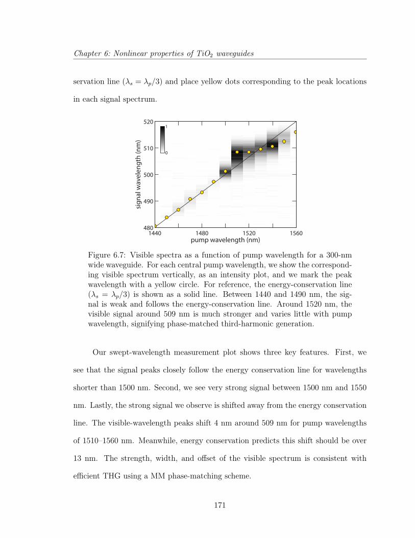
Chapter 6: Nonlinear properties of TiO2 waveguides
servation line (λs = λp/3) and place yellow dots corresponding to the peak locations
in each signal spectrum.
0
1
pump wavelength (nm)
sign
al w
avel
engt
h (n
m)
1440 1480 1520 1560
520
510
500
490
480
Figure 6.7: Visible spectra as a function of pump wavelength for a 300-nmwide waveguide. For each central pump wavelength, we show the correspond-ing visible spectrum vertically, as an intensity plot, and we mark the peakwavelength with a yellow circle. For reference, the energy-conservation line(λs = λp/3) is shown as a solid line. Between 1440 and 1490 nm, the sig-nal is weak and follows the energy-conservation line. Around 1520 nm, thevisible signal around 509 nm is much stronger and varies little with pumpwavelength, signifying phase-matched third-harmonic generation.
Our swept-wavelength measurement plot shows three key features. First, we
see that the signal peaks closely follow the energy conservation line for wavelengths
shorter than 1500 nm. Second, we see very strong signal between 1500 nm and 1550
nm. Lastly, the strong signal we observe is shifted away from the energy conservation
line. The visible-wavelength peaks shift 4 nm around 509 nm for pump wavelengths
of 1510–1560 nm. Meanwhile, energy conservation predicts this shift should be over
13 nm. The strength, width, and offset of the visible spectrum is consistent with
efficient THG using a MM phase-matching scheme.
171
Chapter 6: Nonlinear properties of TiO2 waveguides
6.2.4 Discussion
In the first experiment, we observe that changing waveguide dimensions produces
two distinct phenomena, which we broadly categorize as phase-matched and non-
phase-matched. First, we see weak, broad signal that follows the ESP spectrum for
waveguide widths between 600–800 nm. This is consistent with non-phase-matched
third-harmonic generation near the facet. Second, for the 900-nm wide waveguide,
we observe strong, narrow signal that is within the ESP bandwidth of the pump, but
does not follow the central ESP wavelength. The peak around 526.8 nm is shifted
near the edge of the ESP’s bandwidth, however, we expect that this peak falls within
a spectrally broadened ESP spectrum. The increased efficiency, bandwidth, and
wavelength offset we observe in the 900-nm wide waveguide suggests that only this
waveguide achieves MM phase-matching around 1550 nm.
Comparing our data with simulation allows us to understand and ultimately
control MM phase-matching in TiO2 waveguides. We calculate the total dispersion
for all guided modes from 400 nm to the cutoff condition using a finite-difference
eigenmode solver. For each pair of modes, we calculate the phase-matching wave-
length, if it exists. Additionally, these asymmetrical waveguide geometries do not
support pure TE or TM modes, and instead support hybrid modes (this is particu-
larly the case for higher order modes). To quantify the polarization, we report the
TE-fraction of the mode, given by:
TE− fraction =
∫|Ex|2dxdy∫ (
|Ex|2 + |Ey|2)dxdy
. (6.7)
MM phase-matching only occurs when pumping the fundamental transverse-
electric-like (TE-like) and transverse-magnetic-like (TM-like) modes. We show the
172

Chapter 6: Nonlinear properties of TiO2 waveguides
nearest three phase-matched wavelengths around 1550 nm for a pump in the funda-
mental TE-like mode in Table 6.3. Additionally, we report the TE-fraction calculated
around our starting wavelength of 400 nm for these hybrid modes.
Table 6.3: Phase-matching wavelengths between the fundamental TE-likemode and several higher-order modes in 250-nm thick waveguides with widthsbetween 600 and 900 nm. We present the TE-fraction, calculated around 400nm, to quantify the polarization of these hybrid modes.
600 nm 700 nmpump (nm) 1517.6 1591.4 1614.0 1499.1 1599.9 1652.2signal (nm) 505.9 530.5 538.0 499.7 533.3 550.7TE-fract. 0.969 0.044 0.063 0.928 0.016 0.984
800 nm 900 nmpump (nm) 1564.4 1590.8 1594.1 1555.5 1564.2 1648.9signal (nm) 521.5 530.3 531.4 518.5 521.4 549.6TE-fract. 0.016 0.075 0.076 0.879 0.057 0.033
Our simulation results provide key insights for THG in terms of polarization
and waveguide fabrication. The small, broad signal we observe for the 600 and 700-
nm waveguides is consistent with the absence of phase-matching wavelengths within
the pulse bandwidth. Meanwhile, the 800 and 900-nm wide waveguides have phase-
matching wavelengths within the bandwidth of the pump. The 800-nm wide waveg-
uide is phase-matched around 521.5 nm, however its TE-fraction is low, indicating the
signal mode is cross-polarized with the pump. Similar to second-harmonic generation,
we expect the tensor element responsible for co-polarized THG to be larger than the
cross-polarization term [16]. Therefore, the absence of measurable signal may simply
reflect the lower efficiency. If this is the case, the strongest signal should be for the
900-nm wide waveguide around 518.5 nm. The additional offset we observe may be
173

Chapter 6: Nonlinear properties of TiO2 waveguides
due to variations in the dimensions or material dispersion between the simulated and
fabricated devices. We estimate that a width increase of 20 nm (2.2%) will shift
the 518.5 nm signal to the 521.8 nm we observe experimentally, similarly a width
increase of 47 nm (5.2%) will shift this further to 526.5 nm. These variations are
close to our typical fabrication tolerance (5%). Using simulation as a guide, we see
that both the polarization and specific waveguide dimensions determine the efficiency
phase-matching wavelengths for THG in TiO2 waveguides.
Our swept pump data using a single-waveguide shows that efficient THG de-
pends most strongly on waveguide dimensions. We see two major features that show
both phase-matched and non-phase-matched conditions within the same waveguide.
First, for pump wavelengths between 1510–1550 nm, we observe strong signal that we
attribute to phase-matching. The shift away from the nominal energy conservation
line for pump wavelengths between 1510–1550 nm suggests a visible phase-matched
wavelength of 509 nm. There is a slight tilt in the signal around this 509-nm sig-
nal that corresponds to pump’s central wavelength. The abrupt shift in wavelength
(slightly shifted from the nominal energy conservation line) and strong signal around
1500 nm may be due to an additional phase-matched pump wavelength. Second, the
weak signal we observe from 1440–1490 nm closely follows the scaled pump’s central
wavelength, which is consistent with non-phase-matched THG. Longer transform-
limited pulse durations at shorter wavelengths and uncompensated dispersion may
play a role in the decreased efficiency. We expect that tuning over a wider range
should produce additional phase-matched wavelengths. The signal strengths and off-
sets demonstrate MM phase-matching within this TiO2 waveguide.
174
Chapter 6: Nonlinear properties of TiO2 waveguides
Our preliminary data suggests the process we observe is parametric THG, thus
enabling ultrafast applications. Parametric (instantaneous) processes often require
phase-matching to be efficient and are polarization dependent, as we have observed
experimentally. A non-parametric process adds many complications. For example,
this may be multiphoton absorption followed by fluorescence from a mid-gap state.
In this case, we would expect geometry-independent signals at visible wavelengths,
contrary to our experiments. Additionally, we would require an electronic state for
fluorescence to occur either in TiO2 or in the cladding material, which we do not
expect. Also, the measurement using a silica cladding rules out the fluorescence from
the fluoropolymer cladding. Further experiments to explore the ultrafast dynamics
of this process, such as pump-probe, should determine the true nature of the THG
we observe. Our evidence favors a parametric over a non-parametric process, which
may enable ultrafast frequency conversion between telecommunications and visible
wavelengths.
These results open up many future experiments, applications, and challenges for
THG in TiO2 waveguides. Two-key experiments should be further investigated: quan-
tifying THG efficiency and resolving multiple phase-matched wavelengths within the
same waveguide. These first experiment provide a basis for comparison to other inte-
grated materials and will establishes a stronger link between theory and experiment.
As for applications, our THG device provides a means to convert telecommunica-
tion to visible wavelengths. The narrow bandwidth may enable selective THG from
a wavelength-multiplexed source. Additionally, the sensitivity to waveguide geome-
try suggests thermal tuning is possible. Future work should focus on increasing the
175
Chapter 6: Nonlinear properties of TiO2 waveguides
reliability and efficiency of both generating and extracting THG signal. The geom-
etry sensitivity demands tight fabrication tolerances for predictable phase-matched
wavelengths. Additionally, efficient extraction of the HOM signal is more challenging
than from fundamental modes. Our preliminary results provide a basis for future
experiments and applications utilizing the high efficiency and wavelength specificity
of THG in TiO2 waveguides.
6.2.5 Conclusion
We observe THG in polycrystalline anatase TiO2 waveguides and show that this
process is phase-matched utilizing higher-order waveguide modes. We observe that
phase-matched THG has increased efficiency, a narrow bandwidth, and can have a
wavelength that is offset from the wavelength expected from the central pump wave-
length. Tuning the pump reveals that phase-matching wavelengths are highly depen-
dent on the waveguide’s geometry. Our demonstration of THG in TiO2 waveguides
shows new applications for this exciting material.
176
Chapter 7
Conclusions and outlook
We have explored and developed titanium dioxide for integrated nonlinear optical
devices. We have quantified the optical nonlinearities of bulk rutile TiO2 around 800
nm, which represents the material’s wavelength limit for many all-optical devices.
We have presented a series of studies to produce high-quality thin films of TiO2
suitable for planar integrated photonics. Using these films, we have fabricated linear
waveguides and devices, demonstrating many of the building blocks of more complex
integrated photonic circuits. Lastly, we have explored, observed, and quantified the
first nonlinear optics in TiO2. Having presented the foundation for titanium dioxide
integrated optical circuits, we now summarize the major conclusions and suggest
directions of future research.
Our study of the nonlinear optical properties of bulk TiO2 around 800 nm shows
the onset of two-photon absorption and reveals birefringence in both the nonlinear
index and multiphoton absorption coefficients. Our measurements demonstrate that
two-photon absorption can be avoided in rutile TiO2 by operating at wavelengths as
177

Chapter 7: Conclusions and outlook
short as 813 nm. This is promising for all-optical applications utilizing near-visible
wavelengths, particularly around 850 nm, where two-photon absorption should be
negligible. The low two-photon absorption enables ultra-wide bandwidth devices that
could operate from 800–1600 nm. To support such work, extending bulk measure-
ments to telecommunications wavelengths is both an important and straightforward
study that will serve as the foundation for advanced devices operating throughout
the telecommunications octave (800–1600 nm).
In Chapter 4, we developed high-index optical-quality thin films in both amor-
phous and anatase TiO2 using reactive sputtering. Of these varieties, amorphous
TiO2 has superior losses, particularly for visible wavelengths, and can be deposited
at a higher rate than anatase. The lower losses are likely due to the small grain size
and low surface roughness. Meanwhile, polycrystalline anatase films have a higher
index, yet they exhibit much higher losses. We cannot explain these losses using
surface roughness alone and therefore, we believe scattering from the crystallites (be-
ing comparable to the wavelength) is likely responsible. Even with these increased
losses, they are reasonable when compared to other polycrystalline materials such as
silicon [94–96,154].
To develop the higher-quality thin films necessary for many devices, there are
two paths forward: optimize current thin-film deposition methods or explore alter-
native thin-film sources. Both the amorphous and anatase films can be optimized to
further reduce the losses by exploring the large deposition parameter space. Although
amorphous TiO2 is considerably more consistent, there was some unexplained vari-
ability in both film varieties, resulting in a handful of very high-loss films, even with
178
Chapter 7: Conclusions and outlook
well-established recipes. We have seen improved results from careful wafer handling
and cleaning procedures, as well as pre-depositions to “season” the chamber, which
avoids contamination from previous depositions. Target depletion during long depo-
sitions causes the DC bias voltage to change when using fixed power, and complete
depletion results in the deposition of copper from the target holder. Careful target
control or a series of short deposition may improve results. Improving the losses of
deposited films is an ideal solution that is flexible and scalable, however, the param-
eter space is large and so far, we can only achieve high-quality TiO2 within a narrow
parameter range.
In addition to optimizing the deposition, we recommend exploring alternative
sources of TiO2 thin films. For deposited films, electron-beam evaporation has pro-
duced some reasonable films, however the results were inconsistent. We anticipate
that atomic layer deposition (ALD) should achieve excellent quality films, however,
none of our ALD-deposited films guide. Lastly, we expect single-crystal films should
permit extremely low-loss devices, similar to the benefits of using silicon-on-insulator
wafers versus deposited polycrystalline silicon [94–96]. Single-crystal anatase or ru-
tile may be achievable using epitaxial growth methods on a lattice-matched substrate.
Alternatively, bulk rutile can be adhered to a substrate, then ground to a thickness of
several microns followed by chemical mechanical polishing to produce single-crystal
films. Improving film quality may increase the cost per device, however a high-quality
starting material may be necessary to create devices that can exploit the unique fea-
tures of TiO2.
In Chapter 5, we demonstrated and evaluated waveguides and devices in TiO2
179
Chapter 7: Conclusions and outlook
using visible to telecommunications wavelengths. These devices can serve as the
building blocks for integrated linear and nonlinear optical devices. For linear-optical
devices, we found that amorphous TiO2 outperforms polycrystalline anatase. Similar
to thin films, reducing losses in TiO2 waveguides is necessary for devices, particularly
resonators and nonlinear interferometers. In addition to higher-quality thin films,
refining structuring methods may reduce losses. Even with these challenges, there
are many opportunities to demonstrate new or even well-known devices in this new
material.
In Chapter 6, we explored the first nonlinear optics in anatase TiO2 waveguides.
We observed spectral broadening at wavelengths of 1565 and 794 nm, then extracted
values for n2 nonlinearities of approximately 5 and 50 times silica, respectively. From
the shape of the broadened spectra around 1565 nm, we observed a delayed Raman
nonlinearity that we attribute to the 144 cm−1 Raman line. From this, we estimated
a Raman gain coefficient that is two orders of magnitude greater than silica fiber.
These first nonlinear measurements are promising for TiO2 and demonstrate a strong
nonlinearity over an extended range.
There are several directions for future nonlinear studies and devices. First, a
careful study of the nonlinearity of polycrystalline anatase TiO2 may shed light on
the difference in n2 between 1565 and 794 nm. For devices, we find that losses are the
dominant parasitic effect for both wavelengths studies. Once we reduce the losses,
dispersion engineering will become more effective for telecommunications wavelengths
(1300–1600 nm), enabling devices that utilize four-wave mixing and soliton propaga-
tion. Additionally, increasing the coupling efficiency will be necessary to make energy
180
Chapter 7: Conclusions and outlook
efficient devices. Lastly, the Raman effect is an interesting phenomenon in TiO2
waveguides that we may be exploit for such devices as Raman amplifiers and lasers.
The small energy shift from the Raman line should also avoid many of the problems
of pulse-walk off, leading to more efficient devices.
For nonlinear applications near 800 nm, the material’s group velocity disper-
sion is very strong and normal in both bulk and thin films (–3000 ps/nm/km). This
prohibits efficient four-wave mixing and soliton propagation (due to n2 > 0 for near-
visible wavelengths) without dispersion engineering. Our preliminary studies suggest
that we cannot compensate this strong dispersion around 800 nm using nanowire
dispersion engineering alone. Dispersion engineering may be possible using pho-
ton crystals, adding complimentary materials with anomalous dispersion, or utilizing
higher-order modes for their unique dispersion properties.
We presented our preliminary work on photodarkening in amorphous TiO2 in
Appendix B. Whereas the linear losses of amorphous TiO2 are superior to anatase, we
have observed photodarkening of amorphous TiO2 when films and waveguides were
exposed to femtosecond light pulses around 800 nm. Understanding and avoiding pho-
todarkening will be necessary for integrated nonlinear optical devices in amorphous
TiO2. This preliminary work suggests that the onset of photodarkening may be
related to multiphoton absorption. This implies that for telecommunications wave-
lengths, multiphoton absorption will be a higher order process (i.e. four-photon
instead of two-photon absorption), which may result in a higher threshold for photo-
darkening, allowing for measurement. Additionally, the long-term stability of amor-
phous films should be carefully investigated. If photodarkening can be mitigated,
181
Chapter 7: Conclusions and outlook
nonlinear optical devices in amorphous TiO2 would benefit from the low propagation
losses.
Although there are many ways to improve upon current TiO2 technology, per-
haps the most captivating future applications will exploit the unique properties of
TiO2 in terms of its bandwidth, near-visible compatibility, and its chemical prop-
erties. The high bandwidth of TiO2 should allow for nonlinear optical processing
between widely-spaced communications bands. For example, a signal in the inter-
connect band around 850 nm could control a telecommunications signal around 1550
nm, all within a single chip. Many single and entangled-photon sources as well as
high-efficiency photon counters operate at visible and near-visible wavelengths. Thus,
the extended transparency of TiO2 may be well suited for quantum information ap-
plications. Alternatively, the low-absorption of water for near-visible wavelengths is
excellent for biological applications. Thus, TiO2’s extended wavelength compatibility
and nontoxicity may also enable biophotonic applications such as chemical sensors.
Lastly, TiO2 is a very well-known photocatalyst [184, 185]. Current applications of
bulk and nanoparticle TiO2 include photo-induced water splitting and the decom-
position of organic materials. The high-surface area and strong light confinement
in nanostructured TiO2 waveguides may facilitate light-controlled surface chemical
reactions or self-cleaning devices. We expect further research will identify additional
applications that exploit the distinctive features of TiO2.
The work presented in this thesis lays much of the foundation for TiO2 photon-
ics. Although there are many ways to explore and refine the devices presented here
for all-optical processing applications, TiO2 may also enable novel applications at the
182

Chapter 7: Conclusions and outlook
interface between the fields of integrated photonics, biology, and chemistry. We hope
that future research will unlock the breadth of applications possible in this new and
exciting field of titanium dioxide photonics.
183

Appendix A
Z-scan model for mixed two- and
three- photon absorption
Several reports of modeling multiphoton absorption using the Z-scan method ex-
ist in the literature [23, 79, 186–189]. Models including single nonlinear absorption
mechanisms such as pure 2PA [23], higher-order nonlinear absorption [79], and mixed
multiphoton absorption [186–188] have been presented. In contrast to single absorp-
tion processes, mixed multiphoton absorption is only occasionally observed [190] and
measured [191–193]. Non-idealities, such as ellipticity [189] and laser beam qual-
ity [46, 194], can obscure interpretation of mixed multiphoton data by changing the
shape of the Z-scan curve. For example, beam ellipticity reduces the total signal and
can cause asymmetry [189]. Meanwhile, the beam quality factor, M2, reduces the ap-
parent Rayleigh distance by 1/M2 while maintaining the waist [46, 194, 195]. Mixed
multiphoton absorption is particularly sensitive to such shape changes [186–188].
These effects are not included in the previous models. Thus, we develop a mixed
184

Appendix A: Z-scan model for mixed two- and three- photon absorption
multiphoton absorption model that includes these non-idealities here.
We apply an open aperture Z-scan derivation using an elliptical beam, similar
to that presented in Ref. [189] and highlight the differences. We start with equation
(10) for an elliptical Gaussian beam from reference [189]:
Iin [x, y, z, P (t)] =2P (t)
π wx (z) wy (z)exp
[− 2x2
w2x (z)
− 2y2
w2y (z)
]. (A.1)
Here, z is the sample position, x and y are the transverse spatial coordinates, P (t)
is the instantaneous power as a function of time, and wx(z) and wy(z) are the beam
widths as a function of the sample position, z. We include the beam quality factor
through the width as follows:
wx (z) =
√wx0
2 +
(M2
xλ0
πwx0
)2
(z − zx0)2. (A.2)
In this equation, wx0 is the beam waist,Mx2 is the beam quality factor [195], zx0
is the location of the waist and λ0 is the center wavelength. We use a similar expression
in the y-direction. We define the ellipticity by wx0/wy0 and the astigmatism by zx0zy0.
We include 3PA in the attenuation coefficient, defined for a single wavelength by
α(I) = α0 +α2I+α3I2. Here I is the intensity, and α0, α2, and α3 are the one-, two-,
and three-photon absorption coefficients, respectively. Rutile is highly transparent
for 800 nm, so we set α0 to zero. We solve the following ordinary different equation
using standard numerical methods along the sample length, L:
dI
dz′= −α (I) I (A.3)
Here, z′ is the position inside the sample. We solve for each point in x and y
at a fixed sample position (z). Then, we integrate over x and y at the entrance and
185
Appendix A: Z-scan model for mixed two- and three- photon absorption
exit of the sample to calculate the transmittance (power out normalized to power in).
It should be noted that by following conventional theory [23], we do not include the
effects of self-phase modulation, self-focusing (e.g. filamentation), or dispersion. We
model pulsed transmittance using a Gaussian shape, given by P (t), integrated over
time using:
T (z) =
∫P (t) T [z, P (t) ] dt∫
P (t) dt=Eout (z)
Ein(A.4)
In this equation, T (z) is the observed energy transmittance, T [z, P (t)] is the in-
stantaneous power transmittance, and Ein and Eout are the input and output energies,
respectively. We take into account the reflection from the front surface. Numerical
methods require that we discretize our parameters including the x- and y-position
and time. Consequently, we test for the convergence of all discretization parameters.
Additionally, we find excellent agreement between this model and analytical solutions
for two- [23] and three-photon absorption [79].
Unless otherwise stated, we fit each data set (multiple Z-scan traces at different
powers) using this model to a single set of fit parameters, keeping all others fixed to
experimental values. We fit our data using the Levenberg-Marquardt method. Our fit
parameters are α2, α3, the average z-position of the waist (z0) and the astigmatism.
From this fit, we determine a single value for α2 and α3 that describes the Z-scan
traces for all irradiances measured.
186

Appendix B
Photodarkening in amorphous TiO2
films
Our original aim in this section was to study the nonlinear properties of our optimized
TiO2 films to correlate these results with our bulk TiO2 measurements, however dur-
ing our experiments we discovered an important phenomenon: photo-induced dark-
ening of our amorphous TiO2 films. Compared to bulk samples, the small interaction
lengths in thin films makes studying their nonlinear properties directly using the Z-
scan technique challenging. This is especially the case in anatase thin films, where the
slow deposition rate limits film thickness, making them unsuitable for measurement.
Nonetheless, by exploiting the comparatively high deposition rate of amorphous TiO2,
we have achieved films sufficiently thick to permit nonlinear measurement.
In this section, we summarize our observations of photodarkening in amorphous
TiO2 films. First, we present standard Z-scan measurements which first revealed
photodarkening. Next, we quantify the accumulation of photodarkening using time-
187

Appendix B: Photodarkening in amorphous TiO2 films
dependent transmission measurements. Lastly, we present two measurements of dark-
ened TiO2 to measure electronic and thermal nonlinearities. We will conclude with a
discussion on the implications that photodarkening may have on future devices.
B.1 Standard Z-scan measurements
We perform standard open and closed aperture Z-scan measurements using TiO2
thin films around 800 nm. The signal to background ratio for thin film measurements
is approximately given by tfilmn2film/(tsubstraten2substrate). This ratio must be approx-
imately twice the signal-to-noise ratio (SNR) of the system for proper measurement
(a substrate measurement must be subtracted from the measurement with the film).
For an SiO2 substrate thickness of 500 µm, a SNR of 2%, and an estimated n2 of
8.2 × 10⁻¹⁹ m2/W, we require a minimum film of approximate 1 µm. Considering
this thickness criteria, the low deposition rate of anatase makes proper measurement
impractical and thus, we proceed to measure a 2.2-µm thick amorphous TiO2 film.
B.1.1 Experimental
Our measurement parameters for amorphous TiO2 thin-films are summarized in Table
B.1. Our maximum fluence of 80 mJ/cm2 is well below the reported damage threshold
for TiO2 films (550 mJ/cm2 at 800 nm) [87]. Damage can produce errors that can
be mistaken for Z-scan signal that remains even for low powers [63]. Therefore,
we conduct three sequential measurements to determine the stability of the sample.
First, a low-power measurement provides a pre-baseline, a high-power measurement
shows the nonlinear response of the sample, and a subsequent low-power measurement
188
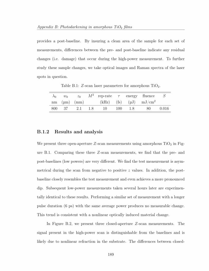
Appendix B: Photodarkening in amorphous TiO2 films
provides a post-baseline. By insuring a clean area of the sample for each set of
measurements, differences between the pre- and post-baseline indicate any residual
changes (i.e. damage) that occur during the high-power measurement. To further
study these sample changes, we take optical images and Raman spectra of the laser
spots in question.
Table B.1: Z-scan laser parameters for amorphous TiO2.
λ0 w0 z0 M2 rep-rate τ energy fluence S
nm (µm) (mm) (kHz) (fs) (µJ) mJ/cm2
800 37 2.1 1.8 10 100 1.8 80 0.016
B.1.2 Results and analysis
We present three open-aperture Z-scan measurements using amorphous TiO2 in Fig-
ure B.1. Comparing these three Z-scan measurements, we find that the pre- and
post-baselines (low powers) are very different. We find the test measurement is asym-
metrical during the scan from negative to positive z values. In addition, the post-
baseline closely resembles the test measurement and even achieves a more pronounced
dip. Subsequent low-power measurements taken several hours later are experimen-
tally identical to these results. Performing a similar set of measurement with a longer
pulse duration (6 ps) with the same average power produces no measurable change.
This trend is consistent with a nonlinear optically induced material change.
In Figure B.2, we present three closed-aperture Z-scan measurements. The
signal present in the high-power scan is distinguishable from the baselines and is
likely due to nonlinear refraction in the substrate. The differences between closed-
189

Appendix B: Photodarkening in amorphous TiO2 films
z/z0
norm
aliz
ed tr
ansm
issi
on
–6 –2 2 6
1.02
1.00
0.98
0.96
0.94
0.92
low (pre): 2 mJ/cm2
z/z0
–6 –2 2 6
full power: 80 mJ/cm2
z/z0
–6 –2 2 6
low (post): 2 mJ/cm2
Figure B.1: Open-aperture Z-scan using a 2.2 µamorphous TiO2 thin film.We see the low-power pre-high-power scan does not match the post-high-power scan, indicating a permanent change.
aperture pre- and post-baselines are comparable to the differences in open-aperture
measurements. We note, there is an asymmetry in the post-baseline measurement,
likely due to misalignment between the laser and translation directions.
z/z0
norm
aliz
ed tr
ansm
issi
on
-6 -2 2 6
1.15
1.10
1.05
1.00
0.95
0.90
low (pre): 2 mJ/cm2
z/z0
-6 -2 2 6
full power: 80 mJ/cm2
z/z0
-6 -2 2 6
low (post): 2 mJ/cm2
Figure B.2: Closed-aperture Z-scan using a 2.2 µamorphous TiO2 thin film.We see the low-power pre-high-power scan does not match the post-high-power scan, indicating a permanent change.
To investigate the potential sample damage, we take optical images of the laser
spots in question at a series of different fluences, shown in Figure B.3 (normal image
on top, color-enhanced on bottom to show spot location). In Figure B.4, we present
a Raman measurement on one of the laser spots, showing no discernible peaks. This
signal is expermentally identical to measurements adjacent to, but away from the laser
spot. We see that the amorphous TiO2 film appears darker with increasing fluence
190
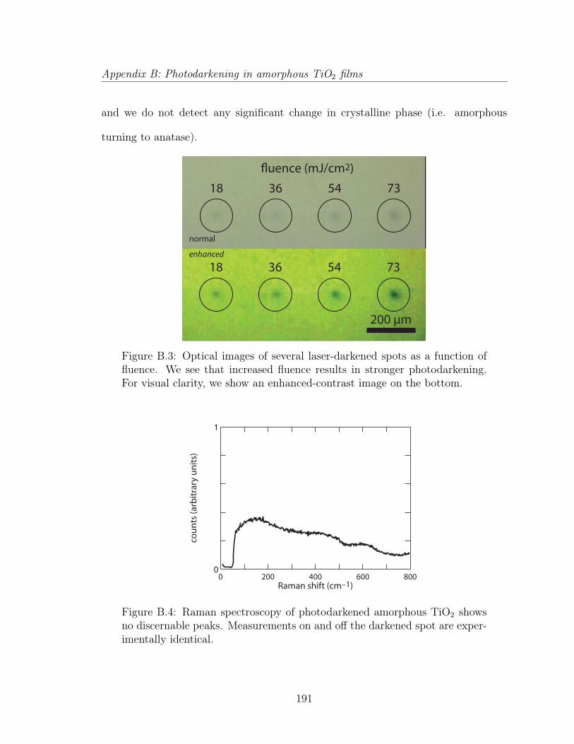
Appendix B: Photodarkening in amorphous TiO2 films
and we do not detect any significant change in crystalline phase (i.e. amorphous
turning to anatase).
200 μm
73543618
73543618
fluence (mJ/cm2)
normal
enhanced
Figure B.3: Optical images of several laser-darkened spots as a function offluence. We see that increased fluence results in stronger photodarkening.For visual clarity, we show an enhanced-contrast image on the bottom.
Raman shift (cm–1)
coun
ts (a
rbitr
ary
units
)
0 200 400 600 800
1
0
Figure B.4: Raman spectroscopy of photodarkened amorphous TiO2 showsno discernable peaks. Measurements on and off the darkened spot are exper-imentally identical.
191
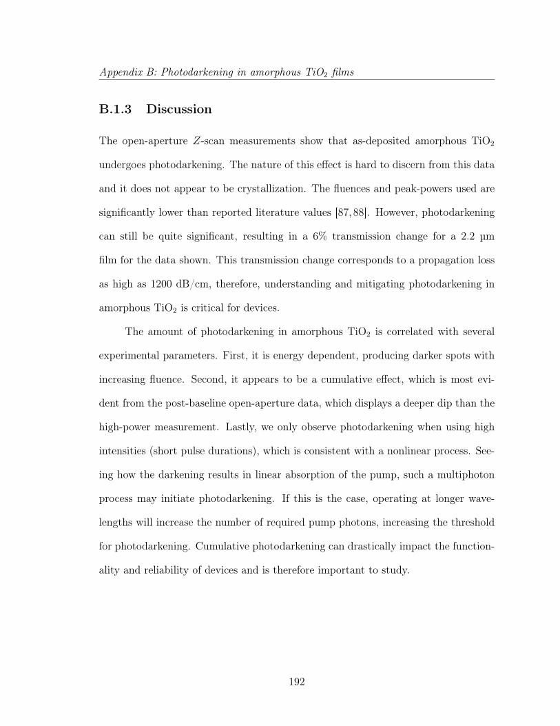
Appendix B: Photodarkening in amorphous TiO2 films
B.1.3 Discussion
The open-aperture Z-scan measurements show that as-deposited amorphous TiO2
undergoes photodarkening. The nature of this effect is hard to discern from this data
and it does not appear to be crystallization. The fluences and peak-powers used are
significantly lower than reported literature values [87, 88]. However, photodarkening
can still be quite significant, resulting in a 6% transmission change for a 2.2 µm
film for the data shown. This transmission change corresponds to a propagation loss
as high as 1200 dB/cm, therefore, understanding and mitigating photodarkening in
amorphous TiO2 is critical for devices.
The amount of photodarkening in amorphous TiO2 is correlated with several
experimental parameters. First, it is energy dependent, producing darker spots with
increasing fluence. Second, it appears to be a cumulative effect, which is most evi-
dent from the post-baseline open-aperture data, which displays a deeper dip than the
high-power measurement. Lastly, we only observe photodarkening when using high
intensities (short pulse durations), which is consistent with a nonlinear process. See-
ing how the darkening results in linear absorption of the pump, such a multiphoton
process may initiate photodarkening. If this is the case, operating at longer wave-
lengths will increase the number of required pump photons, increasing the threshold
for photodarkening. Cumulative photodarkening can drastically impact the function-
ality and reliability of devices and is therefore important to study.
192
Appendix B: Photodarkening in amorphous TiO2 films
B.2 Time-dependent photodarkening
Photodarkening in amorphous TiO2 thin films appears to be a cumulative effect that
can result in strong linear absorption. In this section, we observe the photodarkening
of amorphous TiO2 as a function of time and pulse energy to understand how this
effect accumulates to determine if a parameter space exists that either avoids or
stabilizes photodarkening.
B.2.1 Experiment
We quantify the rate and energy dependence of photodarkening by performing time-
dependent measurement using 100-fs pulses around 800 nm at various pulse energies.
We use the same laser parameters in Table B.1. We start with a clean amorphous TiO2
sample with a thickness of 2.2 µm on a glass substrate. We record the transmission
of our 800-nm laser through the sample as a function of time.
B.2.2 Results and analysis
We present the time dependent transmission in Figure B.5 for several pulse energies.
We observe a stronger change in transmission for higher pulse energies and longer
times. We measure a maximum transmission change of 22% in a 2.2 µm film after a
total exposure time of 4000 seconds (4× 10⁷ shots, 73 mJ/cm2).
The time-dependent transmission change has two distinct features, first we see
a sharp decrease for within the first 500 seconds (5×10⁶ shots). Second, we see a slow
decline in transmission for timescales longer than 1000 second (1 × 10⁷ shots) that
does not appear to saturate over 4000 seconds. We fit each data set to an empirical
193

Appendix B: Photodarkening in amorphous TiO2 films
time (sec x 103)
norm
aliz
ed tr
ansm
issi
on18 mJ/cm2
36 mJ/cm2
54 mJ/cm2
73 mJ/cm2
0 1 2 3 4
1.00
0.96
0.92
0.88
Figure B.5: Time-dependent photodarkening of amorphous TiO2 at severalfluences. We fit this to a bi-exponential function (black lines).
model that takes form of a biexponential:
T (t) = A1 (P ) e−tτ1 + A1 (P ) e
−tτ2 , (B.1)
as shown in Figure B.5. Using this model, we extract two time-scales for photodark-
ening. We find an average short time-scale of τ1 = 350 seconds (3.5× 10⁶ shots) and
an average long timescale of τ2 = 32 hours (1× 10⁹ shots). For increasing pulse ener-
gies, we find A1(P ) increases monotonically while A2(P ) decreases monotonically. In
our fitting the average A1(P ) was 4% and the average A2(P ) was 90%. These values
should total 100%, however the uncertainty in the start time may effect this value.
B.2.3 Discussion
Photodarkening in amorphous TiO2 around 800 nm appears to have two time-scales.
The shortest time-scale is 350 seconds, which is responsible for a maximum change
of 5% for the fluences considered here. Darkening attributed to this short time-scale
194

Appendix B: Photodarkening in amorphous TiO2 films
increases with increasing pulse energy A1(P ). This is consistent with multiphoton
absorption, although we cannot determine the order of the process (i.e two- ver-
sus three-photon absorption) from the current data. Meanwhile, the long-timescale
process decreases when we increase the pulse energy A2(P ).
Photodarkening may be related to a surface chemical reaction. TiO2 is well
known as a photocatalyst, however, such processes require photons which can bridge
the bandgap (3.25 eV, 381 nm). Instead of the linear absorption, this may be due
to nonlinear absorption (i.e. three-photon absorption) that initiates the surface re-
action. Subsequently, the products of this reaction may linearly absorption pump
photons. This strong linear absorption then would lead to local heating, which may
then thermally drive this or a different chemical reaction. Future research should
try to resolve which, if any, chemical reaction may be occurring at the surface of, or
within the film.
Given these two processes, it is difficult to find a pulse energy that is sufficiently
large enough to enable nonlinear measurement while inhibiting photodarkening under
current experimental conditions. However, we do find that for long-time-scales, the
photodarkening saturates, which allows us to measure nonlinearities in photodarkened
TiO2 films.
195
Appendix B: Photodarkening in amorphous TiO2 films
B.3 Thermal nonlinearities in photodarkened amor-
phous TiO2
From the previous section, we have seen how photodarkening is a significant effect
in amorphous TiO2 that saturates with sufficient exposure. Using this stability as a
guide, we now perform two sets of measurements on photodarkened amorphous TiO2
around 800 nm, the first to measure electronic nonlinearities, the second to mea-
sure thermal nonlinearities. In the first measurement, we perform closed-aperture
Z-scan with a repetition rate of 10 kHz to avoid thermal nonlinearities. By com-
paring samples with and without the TiO2 film, we determine the strength of the
electronic nonlinearity. For the second experiment, we perform thermally managed
closed-aperture Z-scan measurements of photodarkened films using a repetition rate
of 250 kHz. This chopper-technique quantifies thermal nonlinearities in our samples
and allows us to resolve the effective sign of dn/dT .
B.3.1 Experiment
We perform two sets of closed-aperture Z-scan measurements using 2.2 µm-thick
photodarkened amorphous TiO2 on 0.5-mm fused silica substrates using the laser
parameters listed in Table B.1. In the first measurement, use a repetition rate of
10 kHz and compare measurements with a thin film to substrate-only measurements.
We guarantee our sample is sufficiently darkened and aligned with our measurement
by conducting multiple Z-scan measurements until we observe reproducible results.
Additionally, the reflection from the front surface changes with and without the film
196

Appendix B: Photodarkening in amorphous TiO2 films
alters the power within the substrate and changes the background signal. Therefore,
we insure that the same energy is within the substrate by adjusting the power so that
we measure the same average power after the sample.
In the second set of measurements we increase the repetition rate to 250 kHz
and perform thermally managed Z-scan. Thermally managed Z-scan uses an optical
chopper to provide a burst of pulses, followed by dead-time to allow the sample to
reach thermal equilibrium. Our chopper has a duty cycle of 6% (4 ms on, 67 ms
off). By comparing Z-scan measurements using data from the beginning and end of
the window, we infer the sign and strength of the effective thermal nonlinearity. In
addition, observing individual time-traces allows us to estimate the time-scale of the
thermal nonlinearity.
B.3.2 Results and analysis
We present two closed aperture Z-scan measurements using a repetition rate of 10
kHz in Figure B.6. We find that adding the film does not produce a change beyond
our estimated experimental uncertainty (±2%). We note that the largest source of
uncertainty comes from matching the power with and without the thin film.
We present two thermally managed Z-scan curves for darkened amorphous TiO2
in Figure B.7. We see at the end of the 4-ms window, the relative Z-scan signal
increases, indicating a positive thermal nonlinearity (dn/dT ) within the film-substrate
system. This effect is quite large, resulting in a ∆T which increases from 15% to 21%.
In Figure B.8 we present time traces for pre- and post- focal positions corre-
sponding to the minimum and maximum transmission values (respectively). Using
197

Appendix B: Photodarkening in amorphous TiO2 films
z/z0
–6 –2 2 6
with TiO2
z/z0
norm
aliz
ed tr
ansm
issi
on
–6 –2 2 6
1.04
1.02
1.00
0.98
0.96
without TiO2
Figure B.6: Closed-aperture Z-scan of the substrate (left) and fully darkenedamorphous TiO2 and substrate (right) at a repetition rate of 10 kHz.
z/z0
–8 –4 0 4 8z/z0
norm
aliz
ed tr
ansm
issi
on
–8 –4 0 4 8
1.10
1.05
1.00
0.95
0.90
0.85
t = 0 ms t = 4 ms
Figure B.7: Thermally managed Z-scan at the beginning (t = 0ms) and end(t = 4ms) of the chopper window. We attribute the differences between theseplots to thermal nonlinearities.
198

Appendix B: Photodarkening in amorphous TiO2 films
this data, we fit to an exponential and find a response time of 0.6 ms in both cases.
time (ms)
norm
aliz
ed tr
ansm
issi
on
0 1 2 3 4
0.94
0.92
0.90
0.88
0.86
time (ms)0 1 2 3 4
1.09
1.08
1.07
1.06
1.05
prefocal postfocal
Figure B.8: Thermally managed Z-scan time-traces during open-chopperwindows at z locations corresponding to the prefocal minimum (left) and thepostfocal maximum (right) transmission.
B.3.3 Discussion
In this section, we look into the electron and thermal nonlinearities in thin films
of amorphous TiO2. We were unable to measure an electronic nonlinearity above
the experimental uncertainty, due to power-matching considerations. To resolve the
electronic nonlinearity, future experiments could utilize a dual-arm Z-scan technique
[196, 197]. In this technique, two matching substrates (with and without the thin
film) are measured simultaneously to remove the effects of the substrate.
Whereas we do not observe clear signal from an electronic nonlinearity, we
measure a thermal nonlinearity that is both strong and positive. Given the size of
the thermal signal, we do not expect that this effect is purely due to the film for two
reasons. First, dn/dT is negative for bulk rutile TiO2 [49] and positive for silica [198].
Second, the magnitude of the change is very large, which would produce a large
value of dn/dT in the TiO2 layer. Although photodarkened amorphous TiO2 may be
199
Appendix B: Photodarkening in amorphous TiO2 films
sufficiently different than rutile, the sign of dn/dT suggests that either the thermal
nonlinearity is positive for the film or (more likely) weak enough to be masked by
the thermal nonlinearity in the silica substrate. Instead, it is reasonable that the
additional absorption caused by the film is diffusing into the silica and the resulting
refractive index change is purely due to the substrate.
The nonlinear signal that we observe in photodarkened amorphous TiO2 is sig-
nificant and can lead to a strong thermal effect which can either be mitigated or
exploited. For many devices, photodarkening may be a mechanism for device failure
both within the TiO2 and within neighbouring components on the same chip. On the
other hand, if this thermal nonliearity leads to local heating, photodarkened TiO2
may be a component used to heat and thermally tune nearby components using an
external laser.
B.4 Conclusion
In this chapter, we have presented several preliminary observation of photodarken-
ing in amorphous TiO2 thin-films. We find that the photodarkening is an important
process, resulting in effective losses as high as 1200 dB/cm. The effect appears to
be nonlinear in nature, it increases with increasing pulse energy and could not be
observed with longer pulse durations of 6 ps. Darkening has two time-scales, one of
only a few minutes while the other is 32 hours. There are several further experiments
that can be performed to determine the source and laser parameter space for photo-
darkening. In particular, future work should look into the microscopic morphology
of laser spots. In addition, TiO2 is a well known photocatalyist, therefore, this phe-
200
Appendix B: Photodarkening in amorphous TiO2 films
nomenon may be related to a chemical reaction that occurs within the laser spot. The
strength of this photodarkening severely limits potential devices using this material,
although some applications may benefit. Understanding the cause of photodarken-
ing may reveal a way to mitigate this effect, which would enable nonlinear devices
that can exploit the very low propagation losses we have demonstrated in amorphous
TiO2.
201

Appendix C
Simulation of TiO2-based Sagnac
interferometers
Now that we have developed TiO2 as a novel integrated material for all-optical pro-
cessing, we will explore one way to enable light-by-light modulation, switching, and
logics: using Sagnac interferometers. In this section, we will look at Sagnac interfer-
ometers as a prototype for all-optical modulation, switching, and logic. We will begin
by developing a simple understanding of these nonlinear devices, then describe how
to form them into simple all-optical logic circuits. Our analysis will be restricted to
self-switching that utilizes the self-phase modulation, for simplicity. Similar results
can be derived for cross-phase modulation [36]. Lastly, we will present simulation
results using typical material parameters for TiO2 and highlight how to design such
devices for all-optical logic applications.
202

Appendix C: Simulation of TiO2-based Sagnac interferometers
C.1 Sagnac interferometers
A Sagnac interferometer, as shown in Figure C.1, is an excellent configuration to
demonstrate all-optical modulation, switching, and logic. These interferometers are
perhaps the simplest nonlinear interferometer configuration achievable in a nanowire
device. These symmetric, self-balancing interferometers utilize counter-propagating
waves and are therefore stable, immune to temperature gradients, and easy to work
with [41,199–201]. Sagnac interferometers provide a tunable balance between switch-
ing energy and device size simply by changing path lengths. These devices are non-
resonant and therefore can sustain extremely high bit-rates [202]. Although we will
only consider all-optical switching and logic as a final application, Sagnac interfer-
ometers are versatile, enabling operations including multiplexing and demultiplexing,
switching, logic [65], and signal regeneration [203].
couplingregion
input transmitted
cw ccw
Figure C.1: Diagram of a Sagnac interferometer showing the input pulse,the coupling region, the clockwise and counter-clockwise paths as well as thetransmitted pulse [204] [36].
To understand how a Sagnac interferometer works, we can consider a nonlinear
interferometer using a quasi-continuous-wave pulse in an interferometer. We form
203

Appendix C: Simulation of TiO2-based Sagnac interferometers
these by making a loop as shown in Figure C.1, then input light into the waveguide
on the left of the loop and observe the output in the waveguide to the right.
The linear version of a Sagnac interferometer acts as a mirror [36]. A pulse enters
the input in Figure C.1, and then encounters a directional coupler. A fraction of the
pulse energy couples into the adjacent waveguide, adding a π/2 phase-shift, then it
propagates around the loop in the counter-clockwise direction. The other fraction
remains within the same waveguide (no phase-shift), and proceeds in the clockwise
direction. These two pulses collect identical amounts of phase as they traverse the
loop and then recombine at the directional coupler. The output is a summation of
the counter-clockwise pulse and the clockwise pulse. The counter-clockwise pulse
picks up a second π/2 phase-shift at the directional coupler, resulting in a total phase
shift of π relative to the clockwise pulse at the output. This phase-shift results in
destructive interference at the output. Meanwhile, constructive interference occurs
on the input-side and the pulse is reflected back toward input, creating a mirror. For
a 50-50 directional coupler, the Sagnac interferometer acts as a ”perfect mirror”. If
the ratio is different from 50-50, part of the light will reach the output.
A Sagnac interferometer can be made nonlinear, sometimes referred to as a
nonlinear optical loop mirror (NOLM) [42,65,200,201,205–213], by forming the loop
using a nonlinear optical material. When traversing the loop, the clockwise and
counter-clockwise pulses collect both linear and nonlinear phase. Both pulses collect
identical linear phase. If the coupling ratio is anything other than 50-50, there will be a
nonlinear phase difference between the pulses, causing power-dependent interference
at the output. Just as we observe fringes in a Michelson interferometer when we
204
Appendix C: Simulation of TiO2-based Sagnac interferometers
change one of the path lengths, we observe power-dependent fringes in a Sagnac
interferometer. These fringes form a basic, all-optical modulator that we can extend
to perform all-optical switching and logic applications. The speed of these devices is
only limited by the response time of the nonlinearity, although a delay in the device
will occur as the pulses propagate. For a pure electronic nonlinearity, this response
is on the order of several femtoseconds [16], making such a device compatible with
Tb/s operations [202].
C.2 Analysis of a Sagnac interferometer
The operation of a nonlinear Sagnac interferometer can be quite complex if we include
all possible effects to correctly model pulse propagation; however, we can get a very
good sense of how one works if we consider a quasi-continuous-wave pulse [36]. Es-
sentially, we modulate a carrier wave with a square envelope, simplifying the analysis
by using a continuous-wave approximation using peak-powers, (not pulse energies).
For this approximation, we ignore dispersion and temporal phenomena, such as spec-
tral broadening. For simplicity, we will also ignore cross-phase modulation between
the counter-propagating pulses. This effect is negligible if the pulse durations are
much shorter than the loop-propagation time. In the continuous-wave regime, cross-
phase modulation is the dominant source of nonlinear phase, however the results are
identical [36].
Analysis in the quasi-continuous-wave regime first requires us to determine the
power that is traveling in the clockwise versus the counter-clockwise directions. We
define a coupling parameter ρ that represents the fraction of the power that stays
205

Appendix C: Simulation of TiO2-based Sagnac interferometers
within the input leg of the directional coupler and traverses the loop in the clockwise-
direction. Thus, ρPin is the clockwise power in the loop, corresponding to an electric
field of magnitude √ρEin, for an input power of Pin and input electric field of Ein.
Similarly, in the counter-clockwise direction, the power and electric field magnitudes
are (1− ρ)Pin and√
1− ρEin, respectively. When we build our devices, we can
change ρ within the directional coupler by adjusting the separation between the two-
waveguides and/or adjusting the distance of the parallel section (described using
coupled-mode theory [14]).
Now, we determine the total phase accumulated in both directions, which re-
quires that we define the length of the loop, L. We consider three sources of phase:
from the directional coupler, linear propagation, and nonlinear propagation. Within
the directional coupler, the power transferred from the input pulse to the counter-
clockwise pulse receives a phase shift of π/2. This phase shift occurs a second time
when the counter-clockwise pulse is transferred to the output, leading to total phase
shift of π for the counter-clockwise pulse only (the clockwise pulse remains in the
original waveguide). Combining this phase-shift with the linear and nonlinear phase
from equation (2.135), we obtain the total phase at the output for the clockwise and
counter-clockwise pulses:
ϕCW = ϕL + ϕCWNL = βL+ γ (ω)LρPin, and (C.1)
ϕCCW = ϕL + ϕCCWNL + ϕDC = βL+ γ (ω)L (1− ρ)Pin + 2 (π/2) . (C.2)
Here, ϕCW is the total phase in the clockwise direction at the output, made up of
a linear and a nonlinear contribution, ϕL and ϕCWNL, respectively. In the counter-
clockwise direction, these terms are ϕCCW , ϕL, and ϕCCWNL, respectively. Addition-
206

Appendix C: Simulation of TiO2-based Sagnac interferometers
ally, there is a phase shift ϕDC from the directional coupler in the counter-clockwise
direction.
Lastly, we sum the electric fields at the output to determine the transmission.
The magnitude of the electric field for the clockwise pulse becomes ρEin at the output,
having picked up an additional factor of √ρ from the directional coupler. Similarly,
the magnitude of the electric field for the counter-clockwise pulse is (1− ρ)Ein at the
output. The electric field at the output is:
Eout = ρEineiϕCW + (1− ρ)Eine
iϕCCW =(ρEine
iϕCWNL − (1− ρ)EineiϕCCWNL
)eiϕL .
(C.3)
We can solve this equation for the transmission to show:
T =|Eout|2
|Ein|2= 1− 2ρ (1− ρ) 1 + cos [(1− 2ρ) γPinL] . (C.4)
From this equation, we see that if ρ is 0.5, the transmission is zero and therefore, we
require that ρ 6= 0.5 to achieve modulation.
We can understand the nature of this device by plotting the output power,
PinT , as a function of the input power, as shown in Figure C.2. We also note that
we can change the spacing of the fringes relative to the input power, using the cou-
pling parameter. For small values of ρ, the fringes are closely spaced in power and
the modulation is minimal. As the coupling parameter ρ approaches 0.5, the first
minimum requires higher powers while the modulation increases.
Although changing the coupling parameters is straightforward experimentally,
simply making longer devices is not always possible and requires that we consider both
linear and nonlinear losses. Linear losses, as we have seen in previously, effectively
207
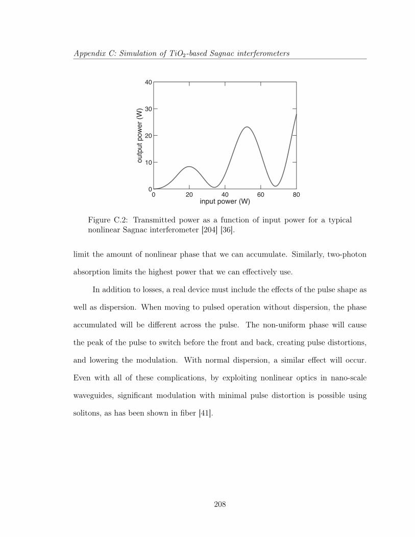
Appendix C: Simulation of TiO2-based Sagnac interferometers
input power (W)
outp
ut p
ower
(W
)
0 20 40 60 80
40
30
20
10
0
Figure C.2: Transmitted power as a function of input power for a typicalnonlinear Sagnac interferometer [204] [36].
limit the amount of nonlinear phase that we can accumulate. Similarly, two-photon
absorption limits the highest power that we can effectively use.
In addition to losses, a real device must include the effects of the pulse shape as
well as dispersion. When moving to pulsed operation without dispersion, the phase
accumulated will be different across the pulse. The non-uniform phase will cause
the peak of the pulse to switch before the front and back, creating pulse distortions,
and lowering the modulation. With normal dispersion, a similar effect will occur.
Even with all of these complications, by exploiting nonlinear optics in nano-scale
waveguides, significant modulation with minimal pulse distortion is possible using
solitons, as has been shown in fiber [41].
208

Appendix C: Simulation of TiO2-based Sagnac interferometers
C.3 All-optical switching
In all-optical switching devices, the power ratio between “on” and “off” states, as
well as the power required for full modulation, are important design considerations.
The ratio of the “off” to the “on” power is the depth of modulation or extinction
ratio [13]. We can approximate the depth of modulation for our Sagnac interferometer
by evaluating equation (C.4) when the argument of the cosine function is equal to π
(the approximate location of the first maximum) and 2π (the approximate location
of the first minimum). The extinction ratio is approximately given by:
Pmax
Pmin
≈ 1
2(1− 2ρ)2 . (C.5)
For example, we find that the extinction ratio reaches 3 dB when ρ = 0.25 and 17 dB
when ρ = 0.45.
Stronger modulation requires higher input powers or longer length devices;
therefore, we consider this trade-off by observing the power required to reach the
first minimum, given by:
Pswitch ≈2π
(1− 2ρ)Lγ. (C.6)
As we approach a coupling ratio of 0.5, the required power for full switching increases
as (1− 2ρ)−1. Comparing this expression to equation (C.5), as ρ approaches 0.5,
the extinction ratio improves as (1− 2ρ)−2. Therefore, we can achieve a substantially
increased extinction ratio for only a moderate operational power increase. In addition,
we can design a longer device to offset the additional power requirements.
209
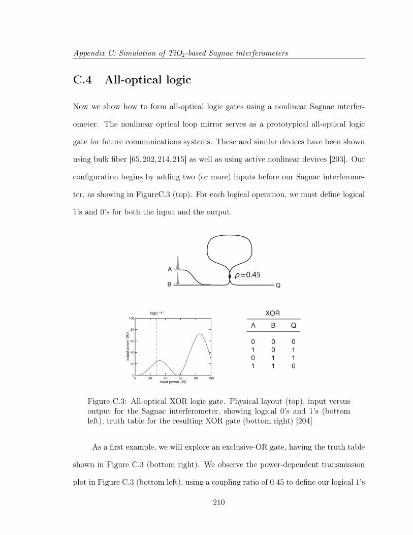
Appendix C: Simulation of TiO2-based Sagnac interferometers
C.4 All-optical logic
Now we show how to form all-optical logic gates using a nonlinear Sagnac interfer-
ometer. The nonlinear optical loop mirror serves as a prototypical all-optical logic
gate for future communications systems. These and similar devices have been shown
using bulk fiber [65,202,214,215] as well as using active nonlinear devices [203]. Our
configuration begins by adding two (or more) inputs before our Sagnac interferome-
ter, as showing in FigureC.3 (top). For each logical operation, we must define logical
1’s and 0’s for both the input and the output.
ρ=0.45
input power (W)
logic “1”
outp
ut p
ower
(W
)
0 20 40 60 80 100
100
80
60
40
20
0
A
QB
A B Q
0 0 0 1 0 1 0 1 1 1 1 0
XOR
Figure C.3: All-optical XOR logic gate. Physical layout (top), input versusoutput for the Sagnac interferometer, showing logical 0’s and 1’s (bottomleft), truth table for the resulting XOR gate (bottom right) [204].
As a first example, we will explore an exclusive-OR gate, having the truth table
shown in Figure C.3 (bottom right). We observe the power-dependent transmission
plot in Figure C.3 (bottom left), using a coupling ratio of 0.45 to define our logical 1’s
210

Appendix C: Simulation of TiO2-based Sagnac interferometers
and 0’s. On the input, a logical 1 has an input power greater of 28 W. On the output,
we define a logical 1 as an output power greater than 18 W. Using the Sagnac’s
transmission function, we can construct the truth table. If neither A nor B is present
at the input, the device produces a logical 0. If only input A or input B is present,
the output is close to the first maximum, resulting in a logical 1. If both A and B are
present at the input, the device produces a logical 0. This demonstrates the truth
table for an XOR gate.
ρ =0.435
input power (W)
logic “1”
outp
ut p
ower
(W
)
0 20 40 60 80 100
100
80
60
40
20
0
A
QB
clock
A B Q
0 0 1 1 0 1 0 1 1 1 1 0
N A N D
Figure C.4: All-optical NAND logic gate. Physical layout (top), input versusoutput for the Sagnac interferometer, showing logical 0’s and 1’s (bottomleft), truth table for the resulting NAND gate (bottom right) [204].
We can construct other gates by adjusting the coupling coefficient, and possibly
adding a clock signal. We are particularly interested in constructing a “universal”
logic gate. These gates can be configured together to form the entire set of Boolean
logic operations. One particular universal logic gate we can construct using a Sagnac
211

Appendix C: Simulation of TiO2-based Sagnac interferometers
interferometer is a NAND gate. A NAND gate has the truth table shown in Figure C.4
(bottom right). As we can see, this gate is more difficult to create than an XOR-gate
because we require a logical 1 when there is no input. Therefore, we add an additional
input to our Sagnac interferometer and deliver a clock pulse with every set of input
pulses. By adjusting our coupling parameter to 0.435, we find that for no inputs in
either A nor B, the clock pulse produces a logical 1 at the output. For an input in
either A or B, the output of the device is around 15 W, constituting a logical 1 at the
output. Now, if both A and B are present, the device reaches the second minimum,
resulting in a logical 0. This prototypical device shows how we can construct an
all-optical NAND gate and thereby create all other Boolean logic gates.
C.5 Pulse propagation in a nonlinear Sagnac inter-
ferometer
These simple continuous wave results provide a clear example of all-optical modulation
in a nonlinear Sagnac interferometer. However, once we include additional effects,
such as dispersion, we quickly see that full-modulation may not be possible even
in a lossless loop as shown in Figure C.5. In this section, we conduct a series of
simulations to determine the parameter range where good modulation is possible in
a Sagnac interferometer with anomalous dispersion.
We simulate nonlinear Sagnac interferometers with different amount of loss and
dispersion to understand how to balance these parameters in a real device. We utilize
a nonlinear-pulse propagation simulation that includes the effects of self-phase mod-
212
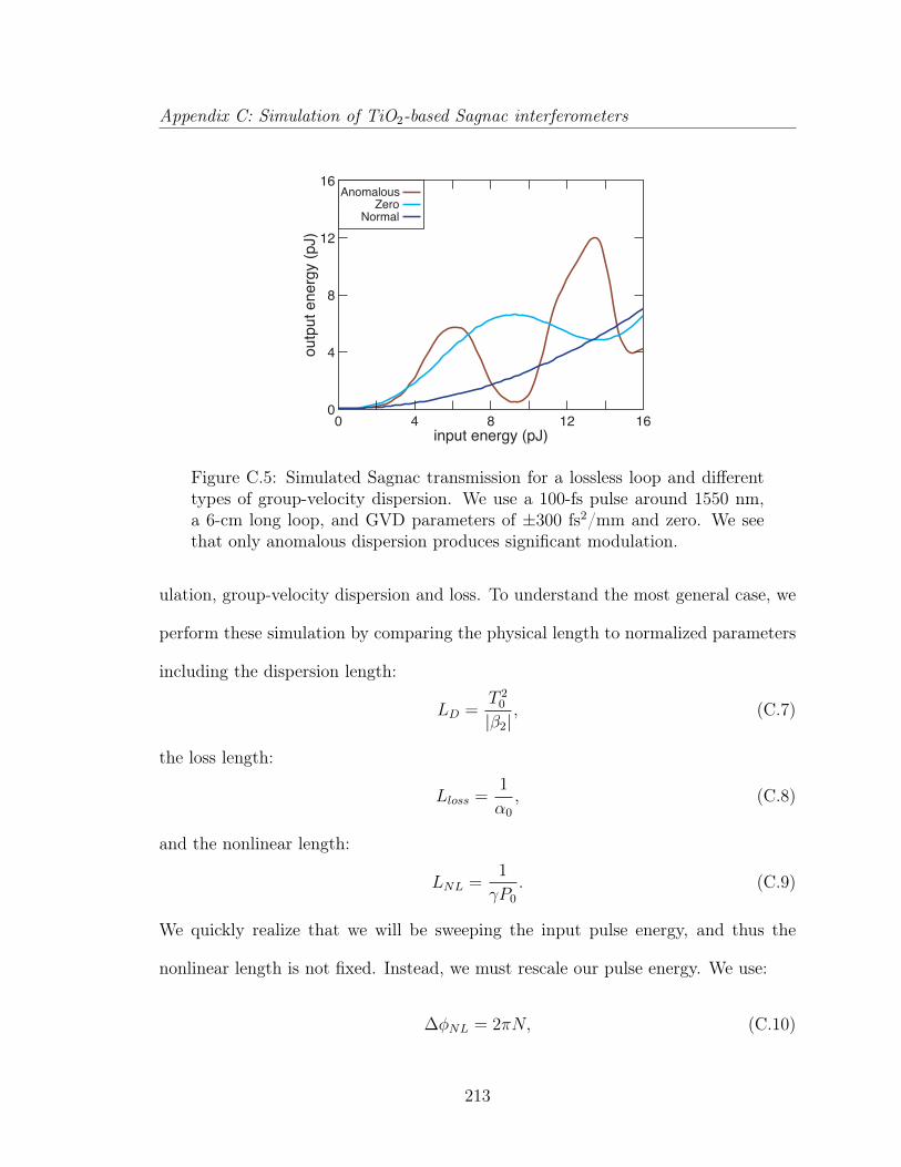
Appendix C: Simulation of TiO2-based Sagnac interferometers
input energy (pJ)
outp
ut e
nerg
y (p
J)
0 4 8 12 16
AnomalousZero
Normal
16
12
8
4
0
Figure C.5: Simulated Sagnac transmission for a lossless loop and differenttypes of group-velocity dispersion. We use a 100-fs pulse around 1550 nm,a 6-cm long loop, and GVD parameters of ±300 fs2/mm and zero. We seethat only anomalous dispersion produces significant modulation.
ulation, group-velocity dispersion and loss. To understand the most general case, we
perform these simulation by comparing the physical length to normalized parameters
including the dispersion length:
LD =T 2
0
|β2|, (C.7)
the loss length:
Lloss =1
α0
, (C.8)
and the nonlinear length:
LNL =1
γP0
. (C.9)
We quickly realize that we will be sweeping the input pulse energy, and thus the
nonlinear length is not fixed. Instead, we must rescale our pulse energy. We use:
∆φNL = 2πN, (C.10)
213
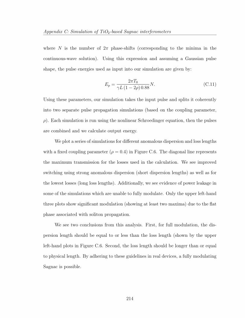
Appendix C: Simulation of TiO2-based Sagnac interferometers
where N is the number of 2π phase-shifts (corresponding to the minima in the
continuous-wave solution). Using this expression and assuming a Gaussian pulse
shape, the pulse energies used as input into our simulation are given by:
Ep =2πT0
γL (1− 2ρ) 0.88N. (C.11)
Using these parameters, our simulation takes the input pulse and splits it coherently
into two separate pulse propagation simulations (based on the coupling parameter,
ρ). Each simulation is run using the nonlinear Schroedinger equation, then the pulses
are combined and we calculate output energy.
We plot a series of simulations for different anomalous dispersion and loss lengths
with a fixed coupling parameter (ρ = 0.4) in Figure C.6. The diagonal line represents
the maximum transmission for the losses used in the calculation. We see improved
switching using strong anomalous dispersion (short dispersion lengths) as well as for
the lowest losses (long loss lengths). Additionally, we see evidence of power leakage in
some of the simulations which are unable to fully modulate. Only the upper left-hand
three plots show significant modulation (showing at least two maxima) due to the flat
phase associated with soliton propagation.
We see two conclusions from this analysis. First, for full modulation, the dis-
persion length should be equal to or less than the loss length (shown by the upper
left-hand plots in Figure C.6. Second, the loss length should be longer than or equal
to physical length. By adhering to these guidelines in real devices, a fully modulating
Sagnac is possible.
214
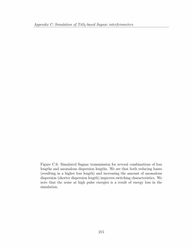
Appendix C: Simulation of TiO2-based Sagnac interferometers
anomalous dispersion length (normalized)
loss
leng
th (n
orm
aliz
ed)
physical length = 1, ρ = 0.4
5
1
0.2
0.2 1 5input energy (normalized)
outp
ut e
nerg
y (n
orm
aliz
ed)
0 1 2 3 40.00
0.01
0.02
0.03
input energy (normalized)
outp
ut e
nerg
y (n
orm
aliz
ed)
0 1 2 3 40.00
0.01
0.02
0.03
input energy (normalized)
outp
ut e
nerg
y (n
orm
aliz
ed)
0 1 2 3 40.00
0.01
0.02
0.03
input energy (normalized)
outp
ut e
nerg
y (n
orm
aliz
ed)
0 1 2 3 40.0
0.5
1.0
1.5
input energy (normalized)
outp
ut e
nerg
y (n
orm
aliz
ed)
0 1 2 3 40.0
0.5
1.0
1.5
input energy (normalized)
outp
ut e
nerg
y (n
orm
aliz
ed)
0 1 2 3 40.0
0.5
1.0
1.5
input energy (normalized)
outp
ut e
nerg
y (n
orm
aliz
ed)
0 1 2 3 40
1
2
3
4
input energy (normalized)
outp
ut e
nerg
y (n
orm
aliz
ed)
0 1 2 3 40
1
2
3
4
input energy (normalized)
outp
ut e
nerg
y (n
orm
aliz
ed)
0 1 2 3 40
1
2
3
4
Figure C.6: Simulated Sagnac transmission for several combinations of losslengths and anomalous dispersion lengths. We see that both reducing losses(resulting in a higher loss length) and increasing the amount of anomalousdispersion (shorter dispersion length) improves switching characteristics. Wenote that the noise at high pulse energies is a result of energy loss in thesimulation.
215
Appendix C: Simulation of TiO2-based Sagnac interferometers
C.6 All-optical switching in TiO2 waveguides
Having developed the guidelines for full modulation in a Sagnac interferometer, we
now define specific goals for future Sagnac interferometers in TiO2 for operation
around 1550 nm. Our current results show that we can achieve losses as low as 3
dB/cm, which corresponds to a loss length of 14 mm at 1550 nm. Our simulation re-
sults show that TiO2 nanowire waveguides can attain anomalous dispersion as strong
as −300 fs2/mm (250 ps/nm/km) resulting in a loss length of 33 mm. If we assume
a 100 fs pulse, this results in a dispersion length of 31 mm. Using this parameter set
as a guide, we show three ways to achieve full modulation.
First, improving losses down to roughly 1 dB/cm will result in loss length of
43 mm. This will result in a functioning device, however the loop length should be
roughly 4 cm. In terms of fabrication on a single chip, this length would require some
variety of coiled structure. Therefore, minimizing bending losses will be an additional
challenge, beyond simply reducing the waveguide losses. Although this device would
fully modulate, the length of the device would be considerably large.
Second, increasing anomalous dispersion to −600 ps/nm/km would result in a
dispersion length of 16 mm, thus approximately matching the loss length. Our cur-
rent simulation results have exclusively explored rectangular nanowire waveguides,
therefore, alternative geometries or photonic crystals may be able to achieve stronger
anomalous dispersion. However, additional complications when fabricating alterna-
tive waveguide geometries can increases the losses substantially (notably in photonic
crystals).
Lastly, using even shorter pulse duration (below 70 fs) would decrease the dis-
216
Appendix C: Simulation of TiO2-based Sagnac interferometers
persion length to coincide with the loss length. This may seem like the simplest
method to first observe all-optical switching in a TiO2 waveguide, however, the addi-
tional bandwidth poses a new challenge. The bandwidth of a 70-fs pulse around 1550
nm is 50 nm (for a Gaussian pulse). For shorter pulses (which would enable signifi-
cantly smaller devices) require even more bandwidth, therefore, common directional
couplers begin to show signs of their frequency dependence.
Perhaps to best way to approach the problem of full modulation in a TiO2
nanowire devices is to simultaneously make slight improvements using all three ap-
proaches. Reducing losses is necessary for many other applications, additionally,
stronger anomalous dispersion may be well within reach, either by optimizing geome-
try or by pairing the device with a shorter pulsed laser. If we can make several small
improvements, a fully modulating TiO2 Sagnac interferometer may be well within
reach.
C.7 Conclusion
We have explored Sagnac interferometers for all-optical modulation, switching, and
logic for use with TiO2 nanowire devices. These unique non-resonant devices show
many advantages for all-optical processing in terms of speed and stability. We have
developed a basic understanding of these devices using simple theory and provided
examples of how to implement switching and logic devices. Lastly, we have conducted
several simulation with realistic parameters to show which combination of physical
parameters (loss, dispersion, and loop-length) results in full modulation and applied
these principles to pinpoint the challenges for future TiO2 devices. By further de-
217

Appendix C: Simulation of TiO2-based Sagnac interferometers
veloping TiO2, we believe that an integrated TiO2 Sagnac interferometer can form
the basic building block of an integrated all-optical logic device for ultrafast signal
processing.
218
Bibliography
[1] R. Essiambre and R. W. Tkach, Proc. IEEE 100, 1035 (2012).
[2] K. F. MacDonald, Z. L. Samson, M. I. Stockman, and N. I. Zheludev, NaturePhoton. 3, 55 (2009).
[3] M. Galili, J. Xu, H. C. Mulvad, L. K. Oxenlowe, A. T. Clausen, P. Jeppesen,B. Luther-Davies, S. Madden, A. Rode, D.-Y. Choi, M. Pelusi, F. Luan, andB. J. Eggleton, Opt. Express 17, 2182 (2009).
[4] B. Corcoran, M. D. Pelusi, C. Monat, J. Li, L. O’Faolain, T. F. Krauss, andB. J. Eggleton, Opt. Lett. 36, 1728 (2011).
[5] Y. Henry Wen, O. Kuzucu, T. Hou, M. Lipson, and A. L. Gaeta, Opt. Lett. 36,1413 (2011).
[6] G. I. Stegeman and W. E. Torruellas, Philos. Trans. R. Soc. London, Ser. A354, 745 (1996).
[7] Q. Lin, J. Zhang, G. Piredda, R. W. Boyd, P. M. Fauchet, and G. P. Agrawal,Appl. Phys. Lett. 91, (2007).
[8] N. Hô, J. M. Laniel, R. al Vallée, and A. Villeneuve, Opt. Lett. 28, 965 (2003).
[9] E. W. Van Stryland, M. A. Woodall, H. Vanherzeele, and M. J. Soileau, Opt.Lett. 10, 490 (1985).
[10] M. Sheik-Bahae, D. J. Hagan, and E. W. Van Stryland, Phys. Rev. Lett. 65,96 (1990).
[11] C. C. Evans, J. D. B. Bradley, E. A. Martì-Panameño, and E. Mazur, Opt.Express 20, 3118 (2012).
[12] D. J. Griffiths, Introduction to electrodynamics, 3rd ed. (Prentice Hall, UpperSaddler River, NJ, 1999).
[13] R. G. Hunsperger, Integrated optics: theory and technology, 6th ed. (Springer,New York, 2009).
219
Bibliography
[14] H. A. Haus, Waves and fields in optoelectronics, (Prentice-Hall, EnglewoodCliffs, NJ, 1984).
[15] Newport Corporation, Application note: Prism Compressor for Ultrashort LaserPulses, 2006.
[16] R. W. Boyd, Nonlinear optics, 3rd ed. (Academic Press, Boston, 2008).
[17] J. M. Chen, J. R. Bower, C. S. Wang, and C. H. Lee, Opt. Commun. 9, 132(1973).
[18] Y. R. Shen, Nature 337, 519 (1989).
[19] R. W. Boyd, Nonlinear optics, 2nd ed. (Academic Press, San Diego, CA, 2003).
[20] G. P. Agrawal, Nonlinear fiber optics, 4th ed. (Elsevier / Academic Press,Boston, 2007).
[21] D. Milam, Appl. Opt. 37, 546 (1998).
[22] M. Sheik-Bahae, D. C. Hutchings, D. J. Hagan, and E. W. Van Stryland, IEEEJ. Quantum. Electron. 27, 1296 (1991).
[23] M. Sheik-Bahae, A. A. Said, T. H. Wei, D. J. Hagan, and E. W. Van Stryland,IEEE J. Quantum. Electron. 26, 760 (1990).
[24] E. W. Van Stryland and M. Sheik-Bahae, in Characterization techniques andtabulations for organic nonlinear optical materials, edited by Mark G. Kuzykand Carl William Dirk (Marcel Dekker, New York, 1998).
[25] G. I. Stegeman, E. M. Wright, N. Finlayson, R. Zanoni, and C. T. Seaton, J.Lightwave Technol. 6, 953 (1988).
[26] G. Stegeman and E. Wright, Opt. Quant. Electron. 22, 95 (1990).
[27] G. I. Stegeman, Proc. SPIE 1852, 75 (1993).
[28] V. R. Almeida, C. A. Barrios, R. R. Panepucci, M. Lipson, M. A. Foster, D. G.Ouzounov, and A. L. Gaeta, Opt. Lett. 29, 2867 (2004).
[29] B. E. A. Saleh and M. C. Teich, Fundamentals of photonics, 2nd ed. (Wiley-Interscience, Hoboken, N.J., 2007), pp. xix, 1177 p.
[30] J. D. Jackson, Classical electrodynamics, 3rd ed. (Wiley, New York, 1999).
[31] D. Gloge, Appl. Opt. 10, 2442 (1971).
[32] D. Marcuse, Appl. Opt. 18, 2930 (1979).
220
Bibliography
[33] V. E. Zakharov and A. B. Shabat, Sov. Phys. JETP 34, 62 (1972).
[34] R. H. Hardin and F. D. Tappert, SIAM Rev. Chronicle 15, 423 (1973).
[35] R. A. Fisher and W. Bischel, Appl. Phys. Lett. 23, 661 (1973).
[36] G. P. Agrawal, Applications of nonlinear fiber optics, 2nd ed. (Elsevier, Boston,2008).
[37] R. Paschotta, Encyclopedia of laser physics and technology (Wiley-VCH, Wein-heim, 2008).
[38] A. Hasegawa and Y. Kodama, Proc. IEEE 69, 1145 (1981).
[39] K. J. Blow and N. J. Doran, Electron. Lett. 19, 429 (1983).
[40] S. Trillo, S. Wabnitz, E. M. Wright, and G. I. Stegeman, Opt. Lett. 13, 672(1988).
[41] K. J. Blow, N. J. Doran, and B. K. Nayar, Opt. Lett. 14, 754 (1989).
[42] M. N. Islam, E. R. Sunderman, R. H. Stolen, W. Pleibel, and J. R. Simpson,Opt. Lett. 14, 811 (1989).
[43] M. A. Foster, K. D. Moll, and A. L. Gaeta, Opt. Express 12, 2880 (2004).
[44] R. Adair, L. L. Chase, and S. A. Payne, Phys. Rev. B 39, 3337 (1989).
[45] S. Leon-Saval, T. Birks, W. Wadsworth, P. St. J. Russell, and M. Mason, Opt.Express 12, 2864 (2004).
[46] P. B. Chapple, J. Staromlynska, J. A. Hermann, T. J. McKay, and R. G. Mc-Duff, J. Nonlinear Opt. Phys. Mater. 6, 251 (1997).
[47] J. Pascual, J. Camassel, and H. Mathieu, Phys. Rev. B 18, 5606 (1978).
[48] D Reyes-Coronado, G Rodríguez-Gattorno, M E Espinosa-Pesqueira, C Cab,R de Coss, and G Oskam, Nanotechnology 19, 145605 (2008).
[49] J. Rams, A. Tejeda, and J. M. Cabrera, J. Appl. Phys. 82, 994 (1997).
[50] Jr G. E. Jellison, L. A. Boatner, J. D. Budai, B. S. Jeong, and D. P. Norton,J. Appl. Phys. 93, 9537 (2003).
[51] J. Li, T. Ishigaki, and X. Sun, J. Phys. Chem. C 111, 4969 (2007).
[52] M. Dinu, IEEE J. Quantum. Electron. 39, 1498 (2003).
221
Bibliography
[53] H. Long, A. Chen, G. Yang, Y. Li, and P. Lu, Thin Solid Films 517, 5601(2009).
[54] T. Hashimoto, T. Yoko, and S. Sakka, Bull. Chem. Soc. Jpn. 67, 653 (1994).
[55] M. Higuchi, T. Hosokawa, and S. Kimura, J. Cryst. Growth 112, 354 (1991).
[56] D. J. Kane and R. Trebino, IEEE J. Quantum. Electron. 29, 571 (1993).
[57] S. Friberg and P. Smith, IEEE J. Quantum. Electron. 23, 2089 (1987).
[58] Y. Watanabe, M. Ohnishi, and T. Tsuchiya, Appl. Phys. Lett. 66, 3431 (1995).
[59] S. Kumar Das, C. Schwanke, A. Pfuch, W. Seeber, M. Bock, G. Steinmeyer, T.Elsaesser, and R. Grunwald, Opt. Express 19, 16985 (2011).
[60] H. A. Castillo-Matadamas, R. M. Lima-García, and R. Quintero-Torres, J. Mod.Optic. 57, 1100 (2010).
[61] E. Portuondo-Campa, A. Tortschanoff, F. van Mourik, and M. Chergui, J.Chem. Phys. 128, (2008).
[62] V. Gayvoronsky, A. Galas, E. Shepelyavyy, T. Dittrich, V. Y. Timoshenko,S. A. Nepijko, M. S. Brodyn, and F. Koch, Appl. Phys. B 80, 97 (2005).
[63] B. M. Patterson, W. Roc White, T. A. Robbins, and R. J. Knize, Appl. Opt.37, 1854 (1998).
[64] R. L. Sutherland, Appl. Opt. 33, 5576 (1994).
[65] M. Jinno and T. Matsumoto, IEEE J. Quantum. Electron. 28, 875 (1992).
[66] M. A. Foster, A. C. Turner, R. Salem, M. Lipson, and A. L. Gaeta, Opt. Express15, 12949 (2007).
[67] A. Penzkofer and W. Falkenstein, Opt. Commun. 17, 1 (1976).
[68] H. S. Waff and K. Park, Phys. Lett. A 32, 109 (1970).
[69] P. Sathy and A. Penzkofer, Appl. Phys. B 61, 127 (1995).
[70] K. Watanabe, K. Inoue, and F. Minami, Phys. Rev. B 46, 2024 (1992).
[71] D. Torres-Torres, M. Trejo-Valdez, L. Castañeda, C. Torres-Torres, L. Tamayo-Rivera, R. C. Fernández-Hernández, J. A. Reyes-Esqueda, J. Muñoz-Saldaña,R. Rangel-Rojo, and A. Oliver, Opt. Express 18, 16406 (2010).
222
Bibliography
[72] M. Trejo-Valdez, R. Torres-Martínez, N. Peréa-López, P. Santiago-Jacinto, andC. Torres-Torres, J. Phys. Chem. C 114, 10108 (2010).
[73] H. Long, G. Yang, A. Chen, Y. Li, and P. Lu, Opt. Commun. 282, 1815 (2009).
[74] M. Kyoung and M. Lee, Bull. Korean Chem. Soc. 21, 26 (2000).
[75] H. I. Elim, W. Ji, A. H. Yuwono, J. M. Xue, and J. Wang, Appl. Phys. Lett.82, 2691 (2003).
[76] L. Irimpan, B. Krishnan, V. P. N. Nampoori, and P. Radhakrishnan, J. ColloidInterface Sci. 324, 99 (2008).
[77] A. H. Yuwono, B. Liu, J. Xue, J. Wang, H. I. Elim, Wei Ji, Ying Li, and T. J.White, J. Mater. Chem. 14, 2978 (2004).
[78] Q. F. Zhou, Q. Q. Zhang, J. X. Zhang, L. Y. Zhang, and X. Yao, Mater. Lett.31, 39 (1997).
[79] D. S. Corrêa, L. De Boni, L. Misoguti, I. Cohanoschi, F. E. Hernandez, andC. R. Mendonça, Opt. Commun. 277, 440 (2007).
[80] S. Couris, M. Renard, O. Faucher, B. Lavorel, R. Chaux, E. Koudoumas, andX. Michaut, Chem. Phys. Lett. 369, 318 (2003).
[81] R. A. Ganeev, A. I. Ryasnyansky, M. Baba, M. Suzuki, N. Ishizawa, M. Turu,S. Sakakibara, and H. Kuroda, Appl. Phys. B 78, 433 (2004).
[82] M. Falconieri and G. Salvetti, Appl. Phys. B 69, 133 (1999).
[83] A. Gnoli, L. Razzari, and M. Righini, Opt. Express 13, 7976 (2005).
[84] K. Watanabe and K. Inoue, Phys. Rev. B 41, 7957 (1990).
[85] C. C. Evans, J. D. B. Bradley, F. Parsy, K. C. Phillips, R. Senaratne, E. A.Martì-Panameño, and E. Mazur, Thermally managed Z-scan measurements oftitanium dioxide thin films, presented at Photonics West, San Francisco, CA,USA, 27 Jan. 2011.
[86] B. Imangholi, M. P. Hasselbeck, and M. Sheik-Bahae, Opt. Commun. 227, 337(2003).
[87] J. Yao, Z. Fan, Y. Jin, Y. Zhao, H. He, and J. Shao, Thin Solid Films 516,1237 (2008).
[88] M. Mero, J. Liu, W. Rudolph, D. Ristau, and K. Starke, Phys. Rev. B 71,115109 (2005).
223
Bibliography
[89] V. G. Ta’eed, N. J. Baker, L. B. Fu, K. Finsterbusch, M. R. E. Lamont, D. J.Moss, H. C. Nguyen, B. J. Eggleton, D. Y. Choi, S. Madden, and B. Luther-Davies, Opt. Express 15, 9205 (2007).
[90] S. J. Madden, D. Y. Choi, D. A. Bulla, A. V. Rode, B. Luther-Davies, V. G.Ta’eed, M. D. Pelusi, and B. J. Eggleton, Opt. Express 15, 14414 (2007).
[91] I. D. Rukhlenko, M. Premaratne, and G. P. Agrawal, Opt. Lett. 35, 55 (2010).
[92] P. Koonath, D. R. Solli, and B. Jalali, Appl. Phys. Lett. 93, 3 (2008).
[93] K. Worhoff, J. D. B. Bradley, F. Ay, D. Geskus, T. P. Blauwendraat, and M.Pollnau, IEEE J. Quantum. Electron. 45, 454 (2009).
[94] J. S. Foresi, M. R. Black, A. M. Agarwal, and L. C. Kimerling, Appl. Phys.Lett. 68, 2052 (1996).
[95] A. M. Agarwal, L. Liao, J. S. Foresi, M. R. Black, X. Duan, and L. C. Kimerling,J. Appl. Phys. 80, 6120 (1996).
[96] L. Liao, D. Lim, A. Agarwal, X. Duan, K. Lee, and L. Kimerling, J. Electron.Mater. 29, 1380 (2000).
[97] J. M. Bennett, E. Pelletier, G. Albrand, J. P. Borgogno, B. Lazarides, C. K.Carniglia, R. A. Schmell, T. H. Allen, T. Tuttle-Hart, K. H. Guenther, and A.Saxer, Appl. Opt. 28, 3303 (1989).
[98] P. K. Tien, Appl. Opt. 10, 2395 (1971).
[99] T. Ohsaka, F. Izumi, and Y. Fujiki, J. Raman Spectrosc. 7, 321 (1978).
[100] M. Yamagishi, S. Kuriki, P. K. Song, and Y. Shigesato, Thin Solid Films 442,227 (2003).
[101] A. Villeneuve, C. C. Yang, P. G. J. Wigley, G. I. Stegeman, J. S. Aitchison,and C. N. Ironside, Appl. Phys. Lett. 61, 147 (1992).
[102] L. Tong, R. R. Gattass, J. B. Ashcom, S. He, J. Lou, M. Shen, I. Maxwell, andE. Mazur, Nature 426, 816 (2003).
[103] V. R. Almeida, C. A. Barrios, R. R. Panepucci, and M. Lipson, Nature 431,1081 (2004).
[104] M. T. Hill, H. J. S. Dorren, T. de Vries, X. J. M. Leijtens, J. Hendrik denBesten, B. Smalbrugge, Y.-S. Oei, H. Binsma, G.-D. Khoe, and M. K. Smit,Nature 432, 206 (2004).
224
Bibliography
[105] H. Park, A. W. Fang, R. Jones, O. Cohen, O. Raday, M. N. Sysak, M. J.Paniccia, and J. E. Bowers, Opt. Express 15, 6044 (2007).
[106] C. Koos, P. Vorreau, T. Vallaitis, P. Dumon, W. Bogaerts, R. Baets, B. Es-embeson, I. Biaggio, T. Michinobu, F. Diederich, W. Freude, and J. Leuthold,Nature Photon. 3, 216 (2009).
[107] X. Guo, M. Qiu, J. Bao, B. J. Wiley, Q. Yang, X. Zhang, Y. Ma, H. Yu, andL. Tong, Nano Lett. 9, 4515 (2009).
[108] B. J. Eggleton, B. Luther-Davies, and K. Richardson, Nature Photon. 5, 141(2011).
[109] R. Espinola, J. Dadap, R. Osgood, S. McNab, and Y. Vlasov, Opt. Express 12,3713 (2004).
[110] R. R. Gattass, G. T. Svacha, L. M. Tong, and E. Mazur, Opt. Express 14, 9408(2006).
[111] R. Dekker, A. Driessen, T. Wahlbrink, C. Moormann, J. Niehusmann, and M.Först, Opt. Express 14, 8336 (2006).
[112] L. Tong, J. Lou, R. R. Gattass, S. He, X. Chen, L. Liu, and E. Mazur, NanoLett. 5, 259 (2005).
[113] T. Tsuchizawa, K. Yamada, H. Fukuda, T. Watanabe, T. Jun-ichi, J. Takahashi,T. Shoji, E. Tamechika, S. Itabashi, and H. Morita, Selected Topics in IEEE J.Quantum. Electron. 11, 232 (2005).
[114] M. A. Foster, A. C. Turner, M. Lipson, and A. L. Gaeta, Opt. Express 16, 1300(2008).
[115] J. T. Choy, B. J. M. Hausmann, T. M. Babinec, I. Bulu, M. Khan, P. Maletinsky,A. Yacoby, and M. Lončar, Nature Photon. 5, 738 (2011).
[116] R. Mechiakh, F. Meriche, R. Kremer, R. Bensaha, B. Boudine, and A. Boudri-oua, Opt. Mater. 30, 645 (2007).
[117] T. Alasaarela, T. Saastamoinen, J. Hiltunen, A. Säynätjoki, A. Tervonen, P.Stenberg, M. Kuittinen, and S. Honkanen, Appl. Opt. 49, 4321 (2010).
[118] J. D. B. Bradley, C. C. Evans, F. Parsy, K. C. Phillips, R. Senaratne, E. Marti,and E. Mazur, in IEEE Photonics Society, 2010 23rd Annual Meeting of the(2010), pp. 313–314.
[119] M. Furuhashi, M. Fujiwara, T. Ohshiro, M. Tsutsui, K. Matsubara, M.Taniguchi, S. Takeuchi, and T. Kawai, AIP Advances 1, 032102 (2011).
225
Bibliography
[120] K. Abe, E. Y. M. Teraoka, T. Kita, and H. Yamada, Proc. of SPIE 7940,79401G–7 (2011).
[121] J. T. Choy, J. D. B. Bradley, P. B. Deotare, I. B. Burgess, C. C. Evans, E.Mazur, and M. Lončar, Opt. Lett. 37, 539 (2012).
[122] Z.-F. Bi, L. Wang, X.-H. Liu, S.-M. Zhang, M.-M. Dong, Q.-Z. Zhao, X.-L. Wu,and K.-M. Wang, Opt. Express 20, 6712 (2012).
[123] N. Sherwood-Droz and M. Lipson, Opt. Express 19, 17758 (2011).
[124] K. Ikeda, R. E. Saperstein, N. Alic, and Y. Fainman, Opt. Express 16, 12987(2008).
[125] S. P. S. Porto, P. A. Fleury, and T. C. Damen, Phys. Rev. 154, 522 (1967).
[126] N. Daldosso, M. Melchiorri, F. Riboli, F. Sbrana, L. Pavesi, G. Pucker, C. Kom-pocholis, M. Crivellari, P. Bellutti, and A. Lui, Mater. Sci. Semicond. Process.7, 453 (2004).
[127] N. Martin, C. Rousselot, D. Rondot, F. Palmino, and René Mercier, Thin SolidFilms 300, 113 (1997).
[128] Y. Vlasov and S. McNab, Opt. Express 12, 1622 (2004).
[129] T. Barwicz and H. I. Smith, J. Vac. Sci. Technol., B 21, 2892 (2003).
[130] M. Gnan, J. Vac. Sci. Technol. B 25, 2034 (2007).
[131] S. Lardenois, D. Pascal, L. Vivien, E. Cassan, S. Laval, R. Orobtchouk, M.Heitzmann, N. Bouzaida, and L. Mollard, Opt. Lett. 28, 1150 (2003).
[132] J. Cardenas, C. B. Poitras, J. T. Robinson, K. Preston, L. Chen, and M. Lipson,Opt. Express 17, 4752 (2009).
[133] R. J. Bojko, J. Li, L. He, T. Baehr-Jones, M. Hochberg, and Y. Aida, J. Vac.Sci. Technol., B 29, 06F309 (2011).
[134] K. J. Vahala, Nature 424, 839 (2003).
[135] M. Lipson, J. Lightwave Technol. 23, 4222 (2005).
[136] E. Shah Hosseini, S. Yegnanarayanan, A. H. Atabaki, M. Soltani, and A. Adibi,Opt. Express 17, 14543 (2009).
[137] C. Kurtsiefer, S. Mayer, P. Zarda, and H. Weinfurter, Phys. Rev. Lett. 85, 290(2000).
226
Bibliography
[138] C. B. Murray, C. R. Kagan, and M. G. Bawendi, Annu. Rev. Mater. Sci. 30,545 (2000).
[139] B. Lounis and W. E. Moerner, Nature 407, 491 (2000).
[140] K. Rivoire, A. Faraon, and J. Vuckovic, Appl. Phys. Lett. 93, 063103 (2008).
[141] M. Barth, N. Nusse, J. Stingl, B. Lochel, and O. Benson, Appl. Phys. Lett. 93,021112 (2008).
[142] M. Khan, T. Babinec, M. W. McCutcheon, P. Deotare, and M. Lon?ar, Opt.Lett. 36, 421 (2011).
[143] Y. Gong and J. Vuckovic, Appl. Phys. Lett. 96, 031107 (2010).
[144] A. Faraon, P. E. Barclay, C. Santori, K.-M. C. Fu, and R. G. Beausoleil, NaturePhoton. 5, 301 (2011).
[145] C. F. Wang, R. Hanson, D. D. Awschalom, E. L. Hu, T. Feygelson, J. Yang,and J. E. Butler, Appl. Phys. Lett. 91, 201112 (2007).
[146] S. A. Campbell, H. S. Kim, D. C. Gilmer, B. He, T. Ma, and W. L. Gladfelter,IBM J. Res. Develop. 43, 383 (1999).
[147] G. Subramania, Y.-J. Lee, A. J. Fischer, and D. D. Koleske, Adv. Mater. 22,487 (2010).
[148] J. D. B. Bradley, C. C. Evans, J. T. Choy, O. Reshef, P. B. Deotare, F. Parsy,K. C. Phillips, M. Lončar, and E. Mazur, Opt. Express 20, 23821 (2012).
[149] M. K. Chin, C. Youtsey, W. Zhao, T. Pierson, Z. Ren, S. L. Wu, L. Wang, Y.Zhao, x, G, and S. T. Ho, IEEE Photon. Technol. Lett. 11, 1620 (1999).
[150] Q. Quan, P. B. Deotare, and M. Loncar, Appl. Phys. Lett. 96, 203102 (2010).
[151] S. Fan, Appl. Phys. Lett. 80, 908 (2002).
[152] L. Zhou and A. W. Poon, Opt. Express 15, 9194 (2007).
[153] A. Guarino, G. Poberaj, D. Rezzonico, R. Degl’Innocenti, and P. Gunter, Na-ture Photon. 1, 407 (2007).
[154] K. Preston, B. Schmidt, and M. Lipson, Opt. Express 15, 17283 (2007).
[155] P. P. Absil, J. V. Hryniewicz, B. E. Little, P. S. Cho, R. A. Wilson, L. G.Joneckis, and P. T. Ho, Opt. Lett. 25, 554 (2000).
227
Bibliography
[156] A. A. Savchenkov, A. B. Matsko, W. Liang, V. S. Ilchenko, D. Seidel, and L.Maleki, Nature Photon. 5, 293 (2011).
[157] Y. Okawachi, K. Saha, J. S. Levy, Y. H. Wen, M. Lipson, and A. L. Gaeta,Opt. Lett. 36, 3398 (2011).
[158] M. A. Foster, J. S. Levy, O. Kuzucu, K. Saha, M. Lipson, and A. L. Gaeta,Opt. Express 19, 14233 (2011).
[159] O. Boyraz and B. Jalali, Opt. Express 12, 5269 (2004).
[160] C. Xiong, L. G. Helt, A. C. Judge, G. D. Marshall, M. J. Steel, J. E. Sipe, andB. J. Eggleton, Opt. Express 18, 16206 (2010).
[161] S. Azzini, D. Grassani, M. J. Strain, M. Sorel, L. G. Helt, J. E. Sipe, M.Liscidini, M. Galli, and D. Bajoni, Opt. Express 20, 23100 (2012).
[162] M. Pollnau, Y. E. Romanyuk, F. Gardillou, C. N. Borca, U. Griebner, S. Rivier,and V. Petrov, Selected Topics in IEEE J. Quantum. Electron. 13, 661 (2007).
[163] F. Koyama, J. Lightwave Technol. 24, 4502 (2006).
[164] J. W. Hall and A. Pollard, Clin. Chem. 38, 1623 (1992).
[165] R. W. Boyd and J. E. Heebner, Appl. Opt. 40, 5742 (2001).
[166] H. Obrig and A. Villringer, JCBFM 23, 1 (2003).
[167] J.-C. G. Bunzli and C. Piguet, Chem. Soc. Rev. 34, 1048 (2005).
[168] R. H. Hadfield, Nature Photon. 3, 696 (2009).
[169] B. S. Wherrett, J. Opt. Soc. Am. B 1, 67 (1984).
[170] M. Dinu, F. Quochi, and H. Garcia, Appl. Phys. Lett. 82, 2954 (2003).
[171] R. M. Osgood, N. C. Panoiu, J. I. Dadap, X. Liu, X. Chen, I. W. Hsieh, E.Dulkeith, W. M. Green, and Y. A. Vlasov, Adv. Opt. Photon. 1, 162 (2009).
[172] J. S. Aitchison, D. C. Hutchings, J. U. Kang, G. I. Stegeman, and A. Villeneuve,IEEE J. Quantum. Electron. 33, 341 (1997).
[173] G. A. Siviloglou, S. Suntsov, R. El-Ganainy, R. Iwanow, G. I. Stegeman, D. N.Christodoulides, R. Morandotti, D. Modotto, A. Locatelli, C. De Angelis, F.Pozzi, C. R. Stanley, and M. Sorel, Opt. Express 14, 9377 (2006).
[174] S. Combrie, Q. V. Tran, A. De Rossi, C. Husko, and P. Colman, Appl. Phys.Lett. 95, 221108 (2009).
228

Bibliography
[175] V. V. Lozovoy, I. Pastirk, and M. Dantus, Opt. Lett. 29, 775 (2004).
[176] L. Yin, Ph.D. thesis, 2009.
[177] K. J. Blow and D. Wood, IEEE J. Quantum. Electron. 25, 2665 (1989).
[178] Q. Lin, O. J. Painter, and G. P. Agrawal, Opt. Express 15, 16604 (2007).
[179] H. Tang, F. Lévy, H. Berger, and P. E. Schmid, Phys. Rev. B 52, 7771 (1995).
[180] Y. R. Shen, The principles of nonlinear optics (Wiley, New York, 1984), pp.xii, 563 p.
[181] A. M. Zheltikov, Phys. Rev. A 72, 043812 (2005).
[182] A. Zheltikov, J. Opt. Soc. Am. B 22, 2263 (2005).
[183] C. C. Evans, K. Shtyrkova, J. D. B. Bradley, O. Reshef, E. Ippen, and E. Mazur,Opt. Express 21, 18582 (2013).
[184] K. Hashimoto, H. Irie, and A. Fujishima, Japanese J. Appl. Phys. Part 1 44,8269 (2005).
[185] A. Fujishima, X. Zhang, and D. A. Tryk, Surf. Sci. Rep. 63, 515 (2008).
[186] B. Gu, J. Wang, J. Chen, Y.-X. Fan, J. Ding, and H.-T. Wang, Opt. Express13, 9230 (2005).
[187] B. Gu, X. Q. Huang, S. Q. Tan, M. Wang, and W. Ji, Appl. Phys. B 95, 375(2009).
[188] J. Wang, B. Gu, X.-W. Ni, and H.-T. Wang, Opt. Laser Technol. 44, 390 (2012).
[189] S. M. Mian, B. Taheri, and J. P. Wicksted, J. Opt. Soc. Am. B 13, 856 (1996).
[190] M. G. Vivas, T. Shih, T. Voss, E. Mazur, and C. R. Mendonça, Opt. Express18, 9628 (2010).
[191] G. Boudebs, S. Cherukulappurath, M. Guignard, J. Troles, F. Smektala, andF. Sanchez, Opt. Commun. 232, 417 (2004).
[192] M. Chattopadhyay, P. Kumbhakar, C. S. Tiwary, A. K. Mitra, U. Chatterjee,and T. Kobayashi, Opt. Lett. 34, 3644 (2009).
[193] T. Sarma, P. K. Panda, P. T. Anusha, and S. V. Rao, Org. Lett. 13, 188 (2010).
[194] A. Eriksson, M. Lindgren, S. Svensson, and P.-O. Arntzen, J. Opt. Soc. Am. B15, 810 (1998).
229

Bibliography
[195] International Organization for Standardization, ISO 11146-1:2005 Lasers andlaser-related equipment - Test methods for laser beam widths, divergence anglesand beam propagation ratios (ISO, Geneva, Switzerland, 2005).
[196] M. R. Ferdinandus, M. Reichert, T. R. Ensley, H. Hu, D. A. Fishman, S. Web-ster, D. J. Hagan, and E. W. Van Stryland, Opt. Mater. Express 2, 1776 (2012).
[197] T. R. Ensley, H. Hu, A. R. Ernst, C. Fuentes-Hernandez, A. Dindar, B. Kippe-len, D. J. Hagan, and E. W. Van Stryland, in Nonlinear Refraction Measure-ments of Thin Films by the Dual-arm Z-scan Method, OSA Technical Digest(online),(Optical Society of America, 2013), p. NTu1B.4.
[198] M. J. Weber, Handbook of optical materials, CRC Press laser and optical scienceand technology series (CRC Press, Boca Raton, 2003), p. 512.
[199] K. Otsuka, Opt. Lett. 8, 471 (1983).
[200] D. B. Mortimore, J. Lightwave Technol. 6, 1217 (1988).
[201] N. J. Doran, D. S. Forrester, and B. K. Nayar, Electron. Lett. 25, 267 (1989).
[202] A. Huang, N. Whitaker, H. Avramopoulos, P. French, H. Houh, and I. Chuang,Appl. Opt. 33, 6254 (1994).
[203] D. Cotter, R. J. Manning, K. J. Blow, A. D. Ellis, A. E. Kelly, D. Nesset, I. D.Phillips, A. J. Poustie, and D. C. Rogers, Science 286, 1523 (1999).
[204] G. Svacha, Ph.D. thesis, 2008.
[205] N. J. Doran and D. Wood, Opt. Lett. 13, 56 (1988).
[206] K. Uchiyama, H. Takara, S. Kawanishi, T. Morioka, M. Saruwatari, and T.Kitoh, Electron. Lett. 29, 1870 (1993).
[207] M. Asobe, T. Ohara, I. Yokohama, and T. Kaino, Electron. Lett. 32, 1396(1996).
[208] L. Jiun-Haw, W. Ding-An, C. Hsin-Jiun, H. Ding-Wei, S. Gurtler, C. C. Yang,K. Yean-Woei, B. C. Chen, M. C. Shih, and T. J. Chuang, IEEE Photon.Technol. Lett. 11, 236 (1999).
[209] M. D. Pelusi, Y. Matsui, and A. Suzuki, IEEE J. Quantum. Electron. 35, 867(1999).
[210] A. Bogoni, M. Scaffardi, P. Ghelfi, and L. Poti, Selected Topics in IEEE J.Quantum. Electron. 10, 1115 (2004).
230
Bibliography
[211] O. Pottiez, E. A. Kuzin, B. Ibarra-Escamilla, J. T. Camas-Anzueto, and F.Gutierrez-Zainos, Electron. Lett. 40, 892 (2004).
[212] E. Simova, I. Golub, and M.-J. Picard, J. Opt. Soc. Am. B 22, 1723 (2005).
[213] M. Sumetsky, Appl. Phys. Lett. 86, 161108 (2005).
[214] M. Jinno and T. Matsumoto, Opt. Lett. 16, 220 (1991).
[215] Y. Miyoshi, K. Ikeda, H. Tobioka, T. Inoue, S. Namiki, and K. Kitayama, Opt.Express 16, 2570 (2008).
231