nonlinear circuits and antennas for microwave
TRANSCRIPT

NONLINEAR CIRCUITS AND ANTENNAS FOR
MICROWAVE ENERGY CONVERSION
by
JOSEPH ALEXEI HAGERTY
B.S., University of Houston, 1998
M.S., University of Colorado, 2001
A thesis submitted to the
Faculty of the Graduate School of the
University of Colorado in partial fulllment
of the requirements for the degree of
Doctor of Philosophy
Department of Electrical and Computer Engineering
2003

This thesis for the Doctor of Philosophy degree by
Joseph Alexei Hagerty
has been approved for the
Department of
Electrical and Computer Engineering
by
Zoya Popovic
Regan Zane
Date
The nal copy of this thesis has been examined by the signatories, and we
nd that both the content and the form meet acceptable presentation
standards of scholarly work in the above mentioned discipline.

Hagerty, Joseph Alexei (Ph.D., Electrical Engineering)
Nonlinear Circuits and Antennas for Microwave Energy Conversion
Thesis directed by Professor Zoya Popovic
This thesis covers theory and experiment for four distinct applications
involving RFDC and DCRF energy conversion between 1 and 18GHz. Mi-
crowave circuits and antennas containing nonlinear elements are used with
high-efficiency operation techniques in a microwave rectier, broadband recti-
fying antenna array, switched-mode oscillator, and switched-mode oscillating
antenna. The applications include dc-dc conversion at microwave switching
speeds, broadband energy recycling with microwave rectifying arrays, and a
high-efficiency transmitting antenna for free-space power combining.
Switched-mode operation for rectiers is discussed in terms of nonlinearly
driven diodes used with proper harmonic terminations and impedance match-
ing. The results are organized in terms of classes of operation in the same
way as is done for microwave ampliers. What is unique for this thesis is the
application of these switched-mode classications to microwave rectiers.
The next topic is a broadband rectenna for low-power ambient energy
recycling (the term rectenna is simply a neologism for rectifying antenna). A
broadband rectenna element and 64-element array are extensively character-
ized for energy recycling of arbitrarily polarized stray elds in the microwave
region to usable DC energy. Concepts gathered from the rectier analysis are
iii

used together with a nonlinear simulation technique and antenna analysis to
design the rectenna and rectenna array.
Next, the class-E mode of amplication is applied to a free-running os-
cillator at 10-GHz. This highly nonlinear, switched-mode class of operation,
which has been documented at 10GHz for ampliers, is analyzed further for
application in a high-efficiency oscillator. The analysis techniques provide
a framework for future, improved versions of the class-E oscillator and the
oscillator is evaluated as the DCRF stage of a DCDC converter.
Finally, a class-E oscillating annular ring antenna for a high-efficiency
transmitting array. An extensive characterization of this active antenna is
presented for class-E operation, antenna geometry, and oscillatory behavior.
Future work is proposed for a 24-element array with a concentration on the
phase-locking and coupling of individual elements.
Future and related work is suggested for each of the four previously men-
tioned topics along with a proposal for new work on a DCDC converter
which makes use of the high-efficiency rectiers and oscillators.
iv

Dedication
To family, friends, and dogs
v

Acknowledgments
I would like to acknowledge, offer thanks, and otherwise recognize the
positive in uence of a few dozen or more friends and colleagues. As a Ger-
man friend pointed out to me, the people on this list might rather appreciate
a beer than a mention on paper, and that offer hereby stands. Nevertheless,
let this list limn historical, from the fall of 1997 to the summer of 2003, my
time in the electromagnetics world.
From the University of Houston:
Lori Basilio, Amit Mehrotra, Stuart Long, Jeff Williams and Michael Khayat
From my brief post as a practicing EMI engineer:
Mark Upcavage
From the beginning at the University of Colorado:
Thanks very much to Zoya Popovic for the tutelage, the nancial support and
the opportunity; Helen Frey, Michael Forman, Wayne Shiroma, and Manoja
vi

Weiss
My forefathers and good friends in the Antenna Lab:
Jan Peeters Weem, Joe Tustin, Jim Vian, and Todd Marshall
My successors and new friends:
Nestor and Ileana, Sebastien Rondineau, Christi Walsh, Alan Brannon, Nar-
isi Wang, Patrick Bell, Matt Osmus, and Deki Filipovic
My contemporaries and friends in suffering:
Paja Pajic, Paul Smith, Darko Popovic, Stefania R•omisch, Rachael Tearle,
Jason Breitbarth, Edeline Fotheringham, and Naoyuki (Nao) Shino
Meinen Deutschen, Osterreichischen, Italienischen, Koreanishen und Bay-
erischen Bekannten und Bierkumpeln bei der Technischen Universitat Munchen:
Florian Helmbrecht, Paul Matyas, Martin Kaleja, Johannes Russer, Fabio
Coccetti, Mark K•uhn, Michael Zedler, Robert Wanner, Jung Han Choi, Klaus
Heppenheimer, Tobias Hermann and Bruno Biscontini
vii

Contents
1 Introduction and Background 1
1.1 Thesis Organization . . . . . . . . . . . . . . . . . . . . . . . . 2
1.1.1 Microwave Rectier . . . . . . . . . . . . . . . . . . . . 2
1.1.2 Microwave Rectifying Array . . . . . . . . . . . . . . . 2
1.1.3 Microwave Oscillator . . . . . . . . . . . . . . . . . . . 3
1.1.4 Microwave Oscillating Antenna . . . . . . . . . . . . . 3
1.1.5 Related and Future Work . . . . . . . . . . . . . . . . 3
1.2 Microwave Energy Conversion . . . . . . . . . . . . . . . . . . 4
1.3 High-Efficiency Operation . . . . . . . . . . . . . . . . . . . . 5
1.4 Analysis Methods . . . . . . . . . . . . . . . . . . . . . . . . . 7
2 RF–DC Conversion:
Microwave Rectifiers 9
2.1 Rectication . . . . . . . . . . . . . . . . . . . . . . . . . . . . 10
2.1.1 Figures of Merit . . . . . . . . . . . . . . . . . . . . . . 11
2.1.2 IV Curves . . . . . . . . . . . . . . . . . . . . . . . . . 13
viii

2.1.3 RF Diode Impedance . . . . . . . . . . . . . . . . . . . 13
2.1.4 Diode Waveforms . . . . . . . . . . . . . . . . . . . . . 15
2.1.5 Diode Matching . . . . . . . . . . . . . . . . . . . . . . 16
2.2 Special Modes of Rectication . . . . . . . . . . . . . . . . . . 17
2.2.1 Class-E Rectication . . . . . . . . . . . . . . . . . . . 17
2.2.2 Class-F Rectication . . . . . . . . . . . . . . . . . . . 19
2.2.3 Inverse Class-E and Class-F . . . . . . . . . . . . . . . 20
2.2.4 Comparison of Waveforms . . . . . . . . . . . . . . . . 20
2.3 Harmonic Terminations . . . . . . . . . . . . . . . . . . . . . . 23
2.3.1 Simulations Using an Exponential Switch . . . . . . . . 24
2.3.2 Simulations Using a Diode Model . . . . . . . . . . . . 26
2.3.3 Measurements . . . . . . . . . . . . . . . . . . . . . . . 27
2.4 Rectier Source-Pulling . . . . . . . . . . . . . . . . . . . . . . 29
2.4.1 Simulated Source Pulls for the Diode Model . . . . . . 29
2.4.2 Measured Source Pulls . . . . . . . . . . . . . . . . . . 32
2.5 Switched Mode Rectier Performance . . . . . . . . . . . . . . 33
2.5.1 Comparison of Simulated and Measured Results . . . . 33
2.5.2 Circuit Designs for Switched Mode Rectiers . . . . . . 36
3 RF Energy Recycling:
A Broadband Rectenna Array 38
3.1 Introduction . . . . . . . . . . . . . . . . . . . . . . . . . . . . 38
3.2 Microwave Rectication and the Rectenna . . . . . . . . . . . 43
ix

3.2.1 Analysis and Design Method . . . . . . . . . . . . . . . 44
3.2.2 Diode Source-Pull . . . . . . . . . . . . . . . . . . . . . 45
3.3 Broadband Rectenna Design . . . . . . . . . . . . . . . . . . . 47
3.3.1 Integrated Rectenna Analysis . . . . . . . . . . . . . . 48
3.3.2 The Spiral Antenna . . . . . . . . . . . . . . . . . . . . 49
3.4 Performance of a Broadband
Rectenna Array . . . . . . . . . . . . . . . . . . . . . . . . . . 52
3.4.1 Array Design . . . . . . . . . . . . . . . . . . . . . . . 53
3.4.2 Frequency Response . . . . . . . . . . . . . . . . . . . 55
3.4.3 DC-Power Response and Radiated Harmonics . . . . . 56
3.4.4 DC Receive Patterns and Polarization . . . . . . . . . 58
3.4.5 A Statistical Study of Multitone Performance . . . . . 60
3.5 Energy Storage and Management for Low Power Applications 62
4 DC–RF Conversion:
Microwave Oscillators 68
4.1 Microwave Oscillators . . . . . . . . . . . . . . . . . . . . . . . 69
4.2 Class-E Operation . . . . . . . . . . . . . . . . . . . . . . . . 72
4.2.1 Class-E Theory . . . . . . . . . . . . . . . . . . . . . . 72
4.2.2 Figures of Merit . . . . . . . . . . . . . . . . . . . . . . 74
4.2.3 Class-E Performance . . . . . . . . . . . . . . . . . . . 75
4.2.4 Diagnostic Tools for Class-E Behavior and Performance 76
x

4.3 Class-E Oscillator Design Based on Class-E Amplier Mea-
surements . . . . . . . . . . . . . . . . . . . . . . . . . . . . . 78
4.3.1 Amplier Measurements for Oscillator Design . . . . . 78
4.4 A low-Q X-Band Class-E Oscillator . . . . . . . . . . . . . . . 81
4.5 Improved class-E Oscillator Design . . . . . . . . . . . . . . . 85
4.5.1 Asymmetric Branch-line Coupler . . . . . . . . . . . . 85
4.5.2 Resonator Design . . . . . . . . . . . . . . . . . . . . . 87
4.5.3 Two-stage Amplier Analysis . . . . . . . . . . . . . . 89
4.5.4 Phase Measurements . . . . . . . . . . . . . . . . . . . 93
4.5.5 Mid-Q Oscillator . . . . . . . . . . . . . . . . . . . . . 94
5 DC–Radiated RF Waves:
A Self-Oscillating Annular Ring 96
5.1 Motivation . . . . . . . . . . . . . . . . . . . . . . . . . . . . . 96
5.2 The Active Ring . . . . . . . . . . . . . . . . . . . . . . . . . 98
5.2.1 Analysis Tools . . . . . . . . . . . . . . . . . . . . . . . 98
5.2.2 Figures of Merit . . . . . . . . . . . . . . . . . . . . . . 100
5.3 Antenna Design . . . . . . . . . . . . . . . . . . . . . . . . . . 101
5.3.1 Lateral Radiation . . . . . . . . . . . . . . . . . . . . . 101
5.3.2 Modal Analysis . . . . . . . . . . . . . . . . . . . . . . 103
5.3.3 Passive Measurements . . . . . . . . . . . . . . . . . . 106
5.4 Antenna and Amplier Integration . . . . . . . . . . . . . . . 107
5.4.1 Class-E Oscillation . . . . . . . . . . . . . . . . . . . . 108
xi

5.4.2 Port Matching . . . . . . . . . . . . . . . . . . . . . . . 109
5.4.3 Loop Analysis . . . . . . . . . . . . . . . . . . . . . . . 113
5.5 Measurements . . . . . . . . . . . . . . . . . . . . . . . . . . . 115
5.5.1 Oscillator Performance . . . . . . . . . . . . . . . . . . 115
5.5.2 Antenna Performance . . . . . . . . . . . . . . . . . . . 117
5.5.3 DCRadiated RF Performance . . . . . . . . . . . . . . 121
5.5.4 A Proposed Active Ring Array . . . . . . . . . . . . . 125
6 Related and Future Work 127
6.1 Microwave Rectication . . . . . . . . . . . . . . . . . . . . . 127
6.2 Low-Power Rectenna Arrays . . . . . . . . . . . . . . . . . . . 128
6.3 Microwave Oscillators . . . . . . . . . . . . . . . . . . . . . . . 129
6.4 Oscillating Antenna Arrays . . . . . . . . . . . . . . . . . . . 131
6.5 DCDC Conversion . . . . . . . . . . . . . . . . . . . . . . . . 132
Bibliography 137
xii

Tables
2.1 Most suitable rectication mode vs. diode reverse break-
down, VrB and series resistance, Rs. . . . . . . . . . . . . . . 23
2.2 1-GHz Rectier simulated results for special modes . . . . . . 35
2.3 1-GHz Rectier measurements for special modes . . . . . . . 35
3.1 Rectication efficiency for a 22 sub-array and the 88 array
with three DC-connection schemes for a low and high incident
power density. Quartiles are dened as the 44 subarrays. . . 57
4.1 Solid-state device selection based on output power and mi-
crowave frequency [1]. . . . . . . . . . . . . . . . . . . . . . . 71
4.2 Comparison of previous work in the eld for high-efficiency
ampliers and oscillators. PSD refers to the power spectral
denisty at a given offset from the carrier. . . . . . . . . . . . 75
4.3 Summary of the two-stage test (refer to Figure 4.9) . . . . . 92
xiii

5.1 Summary of design parameters for the passive ring. The sub-
strate parameters are relative dielectric, r, substrate thick-
ness, h, and metalization layer thickness, t. The physical
parameters of the ring are dened by b and a, the outer and
inner radii. . . . . . . . . . . . . . . . . . . . . . . . . . . . . 106
5.2 Summary of measured parameters for the passive ring. . . . . 107
5.3 Active ring performance for a high-power bias point, high-
efficiency point, compromise between the two, and theoreti-
cally attainable performance. . . . . . . . . . . . . . . . . . . 122
5.4 Comparison of previous work in the eld for oscillator and
amplier elements and arrays. The parameter class refers
to the class of operation in the amplication stage. Refer-
ences marked ∗ are ampliers. The last two rows refer to
the theoretical 24 element array mentioned below based on
the class-E annular ring single element measurements(y) and
theoretically attainable results(z) as given in Table 5.3. . . . 122
xiv

Figures
2.1 Standard rectier (a) and microwave model of the rectier (b) 12
2.2 Simulated (a) and measured (b) IV-curves . . . . . . . . . . . 14
2.3 Simulated voltage and current waveforms for a non-harmonically
terminated diode . . . . . . . . . . . . . . . . . . . . . . . . . 15
2.4 Source-pull diagram for un-terminated case . . . . . . . . . . 16
2.5 Class-F (a) and Class-Ei (b) switch waveforms . . . . . . . . 21
2.6 Class-E (a) and Class-Fi (b) switch waveforms . . . . . . . . 22
2.7 Simulated second and third harmonic termination phase sweeps
for an idealized exponential switch . . . . . . . . . . . . . . . 25
2.8 Simulated second and third harmonic-termination phase sweeps
for the spice model of the diode . . . . . . . . . . . . . . . . 26
2.9 Measured second and third harmonic termination phase sweeps
for the MA4E2054 diode . . . . . . . . . . . . . . . . . . . . 28
2.10 Class-F source-pull diagrams . . . . . . . . . . . . . . . . . . 30
2.11 Class-E source-pull diagrams . . . . . . . . . . . . . . . . . . 30
2.12 Class-Ei source-pull diagrams . . . . . . . . . . . . . . . . . . 31
xv

2.13 Class-Fi source-pull diagrams . . . . . . . . . . . . . . . . . . 31
2.14 Measurement set-up . . . . . . . . . . . . . . . . . . . . . . . 33
2.15 Class-E and class-F measured source-pulls. . . . . . . . . . . 34
2.16 Class-F (a) and class-Ei (b) circuit layouts . . . . . . . . . . 37
2.17 Class-E (a) and class-Fi (b) circuit layouts . . . . . . . . . . 37
3.1 Diagram of various microwave power sources . . . . . . . . . 39
3.2 Block diagram of the rectenna array and control system . . . 41
3.3 Diode test circuit diagrams . . . . . . . . . . . . . . . . . . . 46
3.4 Range of optimal source impedances . . . . . . . . . . . . . . 47
3.5 Measured and Simulated source-pull diagrams . . . . . . . . 48
3.6 Comparison of commercial diodes . . . . . . . . . . . . . . . 49
3.7 Layout of the spiral antenna . . . . . . . . . . . . . . . . . . 50
3.8 Simulated and measured spiral rectenna frequency response . 51
3.9 Simulated and measured Vivaldi-rectenna frequency response 52
3.10 Diagram of the 64-element array . . . . . . . . . . . . . . . . 54
3.11 Frequency response for various input powers . . . . . . . . . 56
3.12 Re ected, rectied, and reradiated power . . . . . . . . . . . 58
3.13 Sampled points for the 3D-DC patterns . . . . . . . . . . . . 59
3.14 Measured DC power patterns . . . . . . . . . . . . . . . . . . 60
3.15 Two-tone power combining measurements . . . . . . . . . . . 61
3.16 Two-tone power increase versus tranmitter frequency . . . . . 63
3.17 Simulated IV-curves . . . . . . . . . . . . . . . . . . . . . . . 65
xvi

4.1 Simulated source-pull (a) and Load-pull (b) . . . . . . . . . . 77
4.2 Class-E amplier PAE,Pout, and G design implications . . . 80
4.3 Drawing of the low-Q 10-GHz oscillator prototype . . . . . . 82
4.4 Power and efficiency contours for the low-Q oscillator prototype 83
4.5 Oscillator Ids, ηosc, and fosc versus Pout . . . . . . . . . . . . 84
4.6 Photograph of the asymmetric branch-line coupler . . . . . . 86
4.7 Photograph of the two-port microstrip ring resonator. . . . . 88
4.8 Schematic of the class-E oscillator . . . . . . . . . . . . . . . 90
4.9 Photograph of the two-stage test amplier . . . . . . . . . . . 91
4.10 Measurements of nonlinear amplier phase response. . . . . . 94
4.11 Photograph of the improved design class-E oscillator . . . . . 95
5.1 Diagram of a self-oscillating antenna . . . . . . . . . . . . . . 97
5.2 Photograph and current distribution of the active ring . . . . 99
5.3 Calculated Eplane patterns vs. b/a ratio . . . . . . . . . . . 102
5.4 Calculated Eplane radiation at azimuth vs. b/a ratio . . . . 103
5.5 Simulated current distributions . . . . . . . . . . . . . . . . . 104
5.6 Mode chart for the annular ring . . . . . . . . . . . . . . . . 105
5.7 Measured and simulated return loss of the passive annular ring107
5.8 Measured and simulated passive radiation patterns . . . . . . 108
5.9 Efficiency and power vs. feedback . . . . . . . . . . . . . . . 110
5.10 Impedance matching for the class-E match . . . . . . . . . . 111
5.11 Impedance matching for the coupling factor . . . . . . . . . . 112
xvii

5.12 Simulated loop gain and phase . . . . . . . . . . . . . . . . . 114
5.13 Measured frequency of oscillation vs. applied gate and drain
bias . . . . . . . . . . . . . . . . . . . . . . . . . . . . . . . . 116
5.14 Measured output power and efficiency vs. applied gate and
drain bias . . . . . . . . . . . . . . . . . . . . . . . . . . . . . 118
5.15 Measured Eplane and Hplane radiation patterns . . . . . . 119
5.16 Measured co and cross-polarized 3D radiation patterns (Mer-
cator) . . . . . . . . . . . . . . . . . . . . . . . . . . . . . . . 120
5.17 Measured co and cross-polarized 3D radiation patterns (or-
thographic) . . . . . . . . . . . . . . . . . . . . . . . . . . . . 120
5.18 Active Antenna Performance . . . . . . . . . . . . . . . . . . 123
5.19 Evidence for class-E match and over-coupling . . . . . . . . . 124
5.20 Proposed phase-locked array . . . . . . . . . . . . . . . . . . 125
6.1 Proposed class-E oscillator with series feedback. . . . . . . . 130
6.2 Drawing of a proposed 10-GHz DCDC converter . . . . . . 134
6.3 10-GHz rectier and computed DCDC converter performance135
xviii

Chapter 1
Introduction and Background
The phrase Nonlinear Circuits and Antennas used in the title of this thesis
refers to passive microwave transmission lines and wave-guiding structures
that are integrated with nonlinear semiconductor devices such as diodes and
transistors. The nonlinearity of the device is used to transfer or convert en-
ergy in one form to another, such as DC to radio frequency (RF). The process
of performing this conversion efficiently using microwave circuit techniques
and nonlinear analysis is the task of this thesis. While energy conversion at
microwave frequencies has been done for over 40 years, the high-efficiency
techniques and applications discussed herein are either less than 8 years old
or introduced here for the rst time.

1.1 Thesis Organization
Four types of microwave energy conversion are covered in this thesis. In
each case, the conversion is between electric potential (the expenditure of
which is referred to as DC), and electromagnetic wave energy both guided
and radiated, in the RF/microwave frequency range.
1.1.1 Microwave Rectifier
The rst form of microwave energy conversion discussed is RF-DC conver-
sion as performed by a microwave rectier (Chapter 2). In this project, a
transmission line loaded with a nonlinear Schottky diode is used to convert
guided RF into usable and/or storable energy for DC loads. Chapter 2 looks
at circuit methods for achieving high efficiency RF-DC conversion at 1GHz
using proper impedance matching and harmonic terminations. The results
are organized into special classes or modes of microwave rectication based
on denitions used for high-efficiency ampliers.
1.1.2 Microwave Rectifying Array
A second kind of RF-DC conversion, free-space RF waves to DC, is addressed
in Chapter 3. Such an instrument is known as a rectenna which is a portman-
teau word for Rectifying Antenna. This converter uses antennas loaded with
diodes at the antenna feed points to capture and convert low-power, stray,
ambient RF as efficiently as possible. The chapter explores solutions for recti-
2

cation of multi-frequency (between 1 and 18GHz), random orientation, and
low-power RF and pursues novel measurement methods of such a system.
1.1.3 Microwave Oscillator
Energy conversion in the reverse direction, DCRF is the topic of Chapters 4
and 5. Chapter 4 looks at the generation of guided RF at 10GHz from DC
in the form of a high-efficiency transmission line oscillator. The important
points in this chapter are methods used and conclusions drawn in designing
a high efficiency oscillator around a high efficiency amplier.
1.1.4 Microwave Oscillating Antenna
Finally, in Chapter 5, an active antenna is presented which efficiently radiates
the RF it converts from DC. The principle of operation is nearly the same
as the oscillator in Chapter 4, only that instead of using a 50Ω output the
feedback loop of the oscillator is used as an antenna. Special attention is
given to the antenna design and overall conversion of DC to RF contained in
the main beam of the antenna.
1.1.5 Related and Future Work
Each of the four converters can be used together for additional forms of
energy conversion as well: A proposed application of the rectenna is for
conversion of stray energy at multiple frequencies rst to DC, then to use
3

the DC over time to intermittently power transmission at another frequency.
Such a system would constitute an RFRF converter involving both an RF
DC and DCRF stage. The DCRF stage can take the form of an oscillator
or amplier in this case.
Conversely, DCDC conversion can be used to regulate and/or provide
Galvonic isolation between a DC-supply and DC-load. This would involve
a DCRF and RFDC stage in the opposite order from the RFRF con-
verter. The reason for performing the energy conversion back and forth from
microwave frequencies is discussed throughout the thesis.
1.2 Microwave Energy Conversion
The term energy conversion is used instead of power conversion throughout
this thesis. The reason stems from the applications and modes of operation
intended for the circuits and antennas discussed: In most of the hypothetic
applications for either RFDC or DCRF conversion the input is typically not
a continuous source. In fact, for the rectenna array (Chapter 3), the input is
a superposition of electromagnetic waves of time varying frequency and am-
plitude. Furthermore, the output is not continuous, but rather stored energy
dissipated intermittently as DC power. The DCRF oscillators may be used
as high-efficiency, battery controlled communication components with strict
power consumption requirements, or as the rst stage in a DCDC converter
with similar constraints. For these reasons the term energy conversion used
4

to emphasize the non-continuous operation of each converter as well as its
application under limited energy reserve.
1.3 High-Efficiency Operation
Semiconductors, composed of materials which become lossier with increas-
ing operation frequency, are also limited by physical dimensions leading to
device reactances which also become signicant at higher frequencies. In
the microwave region, between 1 and 30GHz, semiconductor deciencies are
manifested in the form of ohmic losses in the device. Circuit efficiencies
dened by DCRF, RFDC, RFRF, and DCDC conversion scale directly
with energy consumption and battery lifetime: A circuit with twice the ef-
ciency of another uses half as much power for the same application with
operating twice as long on the same supply. Furthermore, the higher the
efficiency, the less heat is produced.
One way to remedy the losses incurred at higher frequencies is to continue
to tailor the semiconductor for high frequency operation. Such has been done
with MESFET and HEMT technologies which have sought to reduce physi-
cal dimensions, transit times, and loss mechanisms at the expense of power
handling capability. The other approach is to introduce external circuits de-
signed to overcome deciencies in the semiconductor. Such is the purpose of
the well-documented amplier classes B through H and S, [2, 3]. The strategy
of each of these classes of transistor operation is to move the device out of a
5

small-signal, linear regime into a mode which allows greater performance in
terms of power and/or efficiency. Of course improved performance is usually
gained at the expense of linearity and bandwidth. Furthermore, a transistor
driven with nonlinear transconductance, to the point of switch-like behavior,
is necessarily attended by signicant harmonic content. It is typically the de-
gree of nonlinearity (how hard the device is driven and bias level), attention
to the device output impedance (based on device reactances), and storage of
the energy created at the harmonics that is of concern to the high-efficiency
microwave circuit designer.
The rectiers presented in Chapter 2 address the concerns of high effi-
ciency in just this way. A diode driven with a relatively large input (com-
pared to the diode power handling limits) is terminated with appropriate
impedances at DC, the fundamental, and harmonics to shape the diode volt-
age and current waveforms. Optimized waveforms are those which avoid
regions of high ohmic loss in the diode operation. The result is a set of four
rectication classes dened by optimized impedance values for a given diode.
The well-established class-E mode of amplication is used for the oscilla-
tors of Chapter 4 and Chapter 5. This class of operation notably considers
the internal reactance of the device and seeks to control when and when not
energy is stored in the transistor. In this way, ohmic losses are minimized
during the switch-like class-E operation.
The high-efficiency nonlinear regimes discussed here are responsible for
energy conversion ratios 1.2 to 2 times higher than conventional operation
6

modes. The implications this has on energy consumption and battery lifetime
form the crux of the emphasis placed on high-efficiency.
1.4 Analysis Methods
In this thesis an emphasis is placed on measurement solutions to problems
that numerical analysis can not fully address. The nonlinear phenomena
encountered typically have parameters which vary with applied RF power,
frequency, DC power, and harmonic content. Not surprisingly, analytic meth-
ods for optimizing a particular parameter lead quickly to intractable coupled
differential equations. An example can be found in [4] for optimizing DCRF
conversion efficiency in microwave switched-mode amplication. There, the
nonlinearly operated transistor was reduced to a switch circuit element with
harmonic content. For microwave switched-mode oscillators, the dynamics
of chaos and stability also enter the picture, further limiting the power of
numerical analysis.
As nonlinear circuit equations become more complex, the Harmonic Bal-
ance technique becomes indispensable. Explanations of this nonlinear-circuit
analysis method are given in [5, 1]. In [6], for instance, a static analysis of
diode IV characteristics was used to predict RFDC conversion properties
for rectennas. This method was integral in the design of some of the most
important and successful rectenna work to date. In this thesis, a more com-
plex diode analysis is necessary to take into account multiple frequency and
7

harmonic content not taken into account by [6]. In this way HB is used, for
example, to compare rectier performance with various harmonic termina-
tions and for various types of diodes and to study performance trends as a
function of source and load impedances for the class-E oscillator.
In still other cases, HB and the nonlinear models used in HB are simply
not accurate enough to use for a nal circuit design: for example, nding
the operating point for a switched mode oscillator in terms of loop gain,
output power, gate and drain bias, and source and load impedance. In this
case, separate measurements on isolated portions of the oscillator are used to
predict oscillator performance as a function of each of these. This can require
thousands of data points taken over all dimension of interest. In this case
computerized techniques are developed to both take and process the data.
In Chapters 2 and 4, the HB routine from Agilent ADS is used exten-
sively for analysis and design in terms impedance terminations and nonlin-
ear response to power. In Chapter 2 a impedance tuning system known as
a source-pull/load-pull system is used to compare results to the HB simula-
tions. In Chapter 4, the oscillator design relies most heavily on measurements
made on individual components of the oscillator, such as the amplier and
resonator. In Chapter 3, antenna and diode measurements are used in equal
weight with MoM and HB simulations in the rectenna design. Results of the
oscillator study in Chapter 4 are used together with MoM simulations and
eld equations to design the active antenna in Chapter 5.
8

Chapter 2
RF–DC Conversion:
Microwave Rectifiers
Microwave rectication has predominately been used and discussed in the
context of microwave rectennas (rectifying antennas). Rectennas and rec-
tiers have a wide variety of applications including dc-dc conversion [7],
space solar power stations [8], remote actuation [9], signal detection [10],
and stray-energy recycling [11]. In each of these cases high RFDC conver-
sion efficiency is a primary concern. Typically the rectier can be optimized
separately from the antenna or converter as an independent circuit compo-
nent. In the past, this has been done only by impedance matching at the
fundamental frequency. Little attention, however, has been given to study-
ing the effects of properly terminating the harmonic content generated by
the diode during rectication. In this chapter, switched-mode principles of
operation for which proper termination of the harmonics is essential, are ap-
plied to microwave rectiers in much the same way as those methods are
applied to high-efficiency microwave ampliers. The main goal of this chap-
ter is to assess various rectication modes in terms of high and/or optimal
dc-rf conversion efficiency for realistic diodes at microwave frequencies.
2.1 Rectification
Rectication, or ac-dc conversion, has long been understood for low frequency
operation. In its simplest form, a series diode may be used to pass one-half
of the ac-cycle to an RC circuit where the time-varying content is ltered
and only the DC component appears across the load. Such a half-wave
rectier is limited to 50% AC-DC power conversion for an ideal diode. At
microwave frequencies, the rectier circuit must be looked at as a resonant
circuit, containing a nonlinear element (i.e. shunt diode) which traps modes
of the fundamental frequency and its harmonics. If the circuit is matched
at each frequency, the rectier acts as a full-wave rectier (even though only
one diode is used).
In addition to harmonics, the nonlinear diode creates a dc-bias in the res-
onant circuit which can be extracted without affecting the RF characteristics
of the resonant circuit. The time varying voltage and current relationship
at the physical point of the diode in the cavity determines the loss in the
diode and, consequently, the RFDC efficiency. If the cavity is high-Q for the
10

fundamental and harmonics (not much energy is lost in the diode or escapes
the cavity), the dc-rf efficiency can approach 100%. If the RF circuit is well
designed, the losses can be limited to the forward voltage, reverse breakdown
voltage, and series resistance of the diode.
Figure 2.1 depicts the principle of microwave rectication. In the fol-
lowing subsections, the generalized microwave rectier is further explained
before the high-efficiency methods are discussed.
2.1.1 Figures of Merit
The critical denition of efficiency relates the total input power to the the
total DC output power delivered to a load, RL:
ηrf−dc =Prf(in)
Pdc(out)
=Prf(in)
V 2dc/RL
: (2.1)
The main sources of loss are due to I2/R dissipation in the diode, re ected
power at the fundamental, and power lost in the harmonics generated by the
diode. Some have dened a conversion efficiency which does not take into
account the re ected power of the fundamental:
ηconv =Prf(in) − Prf(refl)
Pdc(out)
: (2.2)
This denition only takes into account the efficiency of the diode and not
the efficiency of the entire circuit. The usable DC power is always dened
as the DC power dissipated in a DC load, RL. The re ected power is always
11

(a)
(b)
Figure 2.1: Standard half-wave rectier (a) and microwave model of therectier (b) with impedance matching at dc, the fundamental, and harmonics.
dened here as the power re ected in the fundamental not including the
power lost to the source in the harmonics:
Prefl = P (fo)refl and Prefl−tot =∞Xi=1
P (fi)refl (2.3)
The re ected can also be dened, though not for this study, as the ratio
of the total power re ected at the fundamental and harmonics to Pin.
12

2.1.2 IV Curves
The dc characteristics of a diode can be described by a variable resistor with
an IV relationship given by
I(V ) = Is(eV
KT/q − 1): (2.4)
A very convenient way of predicting rectier behavior and identifying loss
mechanisms is by using diode IV curves relating the drawn current to the
applied diode voltage. Figure 2.2 (a) and Figure 2.2 (b) show IV curves for
Equation 2.4, the Spice model of a MA4E2054, and the measured curves for
the the MA4E2054 and SMS7630 diodes.
2.1.3 RF Diode Impedance
To compute the input impedance of a diode, Zin(!, V ), the expression
Gd =1
Rj
=dI
dV
V =Vo
(2.5)
can be used to include the voltage dependence. Since we also have the for-
mula relating current and voltage across the nonlinear resistor given in Equa-
tion 2.4, a Taylor expansion can be used to obtain
Rj =1
IseV jV =Vo
(2.6)
for small signals. To calculate Zin the junction capacitance Cj, package
inductance Lp, package capacitance Cp, and series resistance Rs, are included
13

−7 −6 −5 −4 −3 −2 −1 0 1 2−40
−30
−20
−10
0
10
20
30
40
Voltage [V]
Cur
rent
[mA
]
current
−7 −6 −5 −4 −3 −2 −1 0 1 2−50
−40
−30
−20
−10
0
10
20
Pow
er [dBm
]
dissipated power
exponentialswitch
−7 −6 −5 −4 −3 −2 −1 0 1 2−40
−30
−20
−10
0
10
20
30
40
Voltage [V]
Cur
rent
[mA
]
MA4E2054
−7 −6 −5 −4 −3 −2 −1 0 1 2−40
−30
−20
−10
0
10
20
30
40
Current [m
A]
SMS7630
(a) (b)
Figure 2.2: Simulated (a) and measured (b) IV-curves. The curves in (a)are for an exponential and Spice model of the MaCom MA2E2054 Schottkydiode. The measured characteristic of the MA2E2054 is compared in (b)with the Alpha SMS7630 diode used in Chapter 3. In (a) it is also shownhow the power dissipated in the diode is large in the case of operation nearthe reverse breakdown region.
in parallel with Rj so that
Zin = Cp k (Lp + Rs + Cj k Rj) (2.7)
and nally
Zin(!, V ) =
j!Cp + (j!Lp + Rs +
1
IseV + j!Cj
)−1
−1
: (2.8)
However, Equation 2.8 is a only a useful predictor of the nonlinear diode
input impedance under small-signal conditions. As with similar denitions
of small-signal transistor input and output impedances, this denition is of
limited use when large-signal matching of the fundamental frequency and
harmonics are necessary.
14

For this reason, the Harmonic Balance (HB) method of nonlinear circuit
analysis is used here to simulate and analyze the RF rectier. HB intrinsically
uses Equation 2.4 and the equivalent circuit represented by Equation 2.8. In
addition, HB takes into account the energy at DC, the fundamental fre-
quency, and a specied number of harmonics in the circuit.
0 0.5 1 1.5 2
0
2
4
6
8
10
12
Time [ns]
Vol
tage
[V
]
Voltage
0 0.5 1 1.5 2
0
10
20
30
40
50
60
Current [m
A]
Current
Matched case
No terminations
Figure 2.3: Simulated voltage and current waveforms at 1GHz for a diodematched at the fundamental for efficiency without additional matching forthe harmonics. Waveforms appear across a switch modeled by an exponentialcurve in parallel with a capacitor.
2.1.4 Diode Waveforms
The simulated waveform of Figure 2.3 is obtained using HB in Agilent ADS
for a variable resistor given by Equation 2.4 in parallel with a junction ca-
pacitance of 0.1 pF. The idealized diode is matched at the fundamental fre-
quency for optimal rectication efficiency. The voltage and current levels
15
can be compared to Figure 2.2 (a) to see how normal operation of the diode
breaches the high-loss regions of the IV curve. If either of the Spice models
had been used, the voltage waveform would have been clipped at the reverse
breakdown voltage.
0.2 0.5 1 2
j0.2
−j0.2
0 ∞
j0.5
−j0.5
0 ∞
j1
−j1
0 ∞
j2
−j2
0 ∞
30
40
40
45
45
45
5055
45
0.2 0.5 1 2
j0.2
−j0.2
0 ∞
j0.5
−j0.5
0 ∞
j1
−j1
0 ∞
j2
−j2
0 ∞
−3 −6−9 −12
(a) (b)
Figure 2.4: Source-pull diagram of the un-harmonically terminated case.Rf-dc conversion efficiency (a) normalized rf re ected power (b). Contoursof constant efficiency [%] and relative re ected power [db] are plotted overvarying source impedance.
2.1.5 Diode Matching
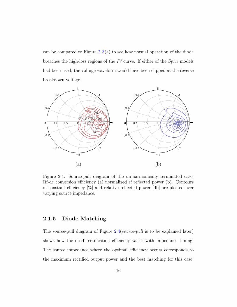
The source-pull diagram of Figure 2.4(source-pull is to be explained later)
shows how the dc-rf rectication efficiency varies with impedance tuning.
The source impedance where the optimal efficiency occurs corresponds to
the maximum rectied output power and the best matching for this case.
16

However, this case does not include harmonic terminations. Later sections
show how proper impedance matching at the fundamental, DC and harmon-
ics can improve the efficiency further.
2.2 Special Modes of Rectification
Class-E behavior was rst introduced in the context of an amplier by Sokal
and Sokal in 1975 [12]. The theory was modied in 1988 in [13] for rectiers
to be used in high-efficiency DC-DC converters [14, 15]. In both cases the
frequency of operation was around 1MHz. Mader further developed class-
E theory for transmission line ampliers at microwave frequencies in 1995
[16]. Mader's work is modied here, for the rst time, for microwave trans-
mission line rectiers. The outline of Mader's approach is paraphrased here
for brevity and details are left out where they are identical to his original
analysis.
2.2.1 Class-E Rectification
The development of the simplied class-E rectier theory begins with the as-
sumptions that 100% RFDC efficiency can be achieved with an ideal switch
in parallel with a linear capacitance, Cs. This corresponds to the nonlinear
resistor, Rj, and the junction capacitance, Cj, in the diode. The RF volt-
age that drives the switch is assumed to generate a 50% duty cycle. During
the OFF (open) cycle of the switch, Cs stores energy which is partially dis-
17
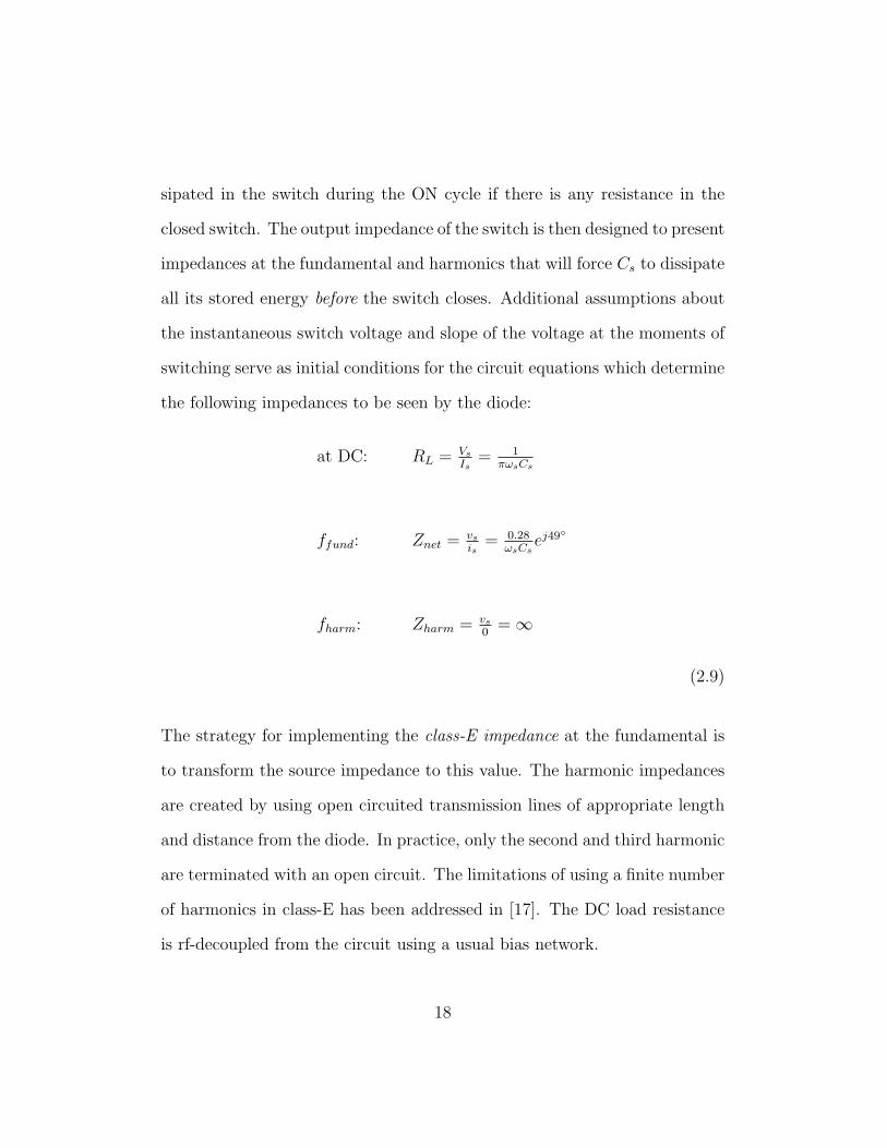
sipated in the switch during the ON cycle if there is any resistance in the
closed switch. The output impedance of the switch is then designed to present
impedances at the fundamental and harmonics that will force Cs to dissipate
all its stored energy before the switch closes. Additional assumptions about
the instantaneous switch voltage and slope of the voltage at the moments of
switching serve as initial conditions for the circuit equations which determine
the following impedances to be seen by the diode:
at DC: RL = Vs
Is= 1
π!sCs
ffund: Znet = vs
is= 0:28
!sCsej49
fharm: Zharm = vs
0= 1
(2.9)
The strategy for implementing the class-E impedance at the fundamental is
to transform the source impedance to this value. The harmonic impedances
are created by using open circuited transmission lines of appropriate length
and distance from the diode. In practice, only the second and third harmonic
are terminated with an open circuit. The limitations of using a nite number
of harmonics in class-E has been addressed in [17]. The DC load resistance
is rf-decoupled from the circuit using a usual bias network.
18

In order to solve for the anticipated Vdc, Idc, v(t)max, and i(t)max, Equa-
tion 2.9 must be solved for using VdcIdc = Pin for 100% efficiency. The
resulting class-E voltage and current waveforms across the switch-element of
the diode are shown in Figure 2.6. As will be shown, this rst order ap-
proximation of the class-E impedances will have limitations for large signal
operation and alternative design methods are discussed and proposed.
2.2.2 Class-F Rectification
Class-F theory has been developed in a less extensive manner than class-
E for microwave transmission line circuits. The critical aspect of class-F
behavior is the wave-shaping accomplished by the harmonic terminations:
even harmonics are terminated with an open circuit, odd harmonics with
a short circuit such that the switch voltage achieves a square wave shape.
The determination of the fundamental impedance is designed for maximal
power transfer to the load in the case of an amplier. It has been shown
that a real impedance equal to 2Vds/Idss can be used (even in saturation)
for the fundamental impedance. However, like the class-E impedances, the
optimal fundamental impedance for class-F will be better found using non-
linear simulation techniques rather than rst order approximations.
19

2.2.3 Inverse Class-E and Class-F
The less common inverse modes of class-E and class-F are dened by their
harmonic terminations which are opposite in phase angle from their counter-
parts. In inverse class-E, or class-Ei, each harmonic termination is a short
circuit. The class-Ei circuit design and switch waveforms bear no resemblance
to class-E and do not employ the philosophy of draining the stored charge in
Cs before the switch turns on. Similarly, in class-Fi, the even harmonics are
terminated with a short circuit and the odd harmonics with opens. In both
cases there are no design guidelines for the optimal DC and fundamental
impedances. Therefore, nonlinear simulations will be used to nd these. The
reason for considering these two classes for rectiers is that class-Ei has a
short conduction period and high current peak, while class-Fi has a squared
current waveform. Each case can provide special advantages and disadvan-
tages depending on the diode, RF input level, and/or load resistance.
2.2.4 Comparison of Waveforms
The effect of these special cases of impedance terminations on the diode
waveforms are demonstrated in this section for an idealized rectier at 1GHz
with a diode based on Equation 2.4 in parallel with a capacitor. The same
scale is used for each case as was used in Figure 2.3 for the matched diode.
Each waveform is also taken at the optimal fundamental impedance and DC
load resistance for that particular mode.
20
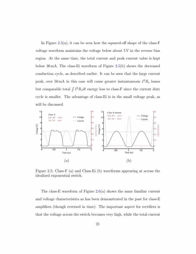
In Figure 2.5(a), it can be seen how the squared-off shape of the class-F
voltage waveform maintains the voltage below about 5V in the reverse bias
region. At the same time, the total current and peak current value is kept
below 30mA. The class-Ei waveform of Figure 2.5(b) shows the decreased
conduction cycle, as described earlier. It can be seen that the large current
peak, over 50mA in this case will cause greater instantaneous I2Rs losses
but comparable totalR
I2Rsdt energy loss to class-F since the current duty
cycle is smaller. The advantage of class-Ei is in the small voltage peak, as
will be discussed.
0 0.5 1 1.5 2
0
2
4
6
8
10
12
Time [ns]
Vol
tage
[V]
Voltage
0 0.5 1 1.5 2
0
10
20
30
40
50
60
Current [m
A]
Current
Class−F 2nd, 4th − short3rd, 5th − open
0 0.5 1 1.5 2
0
2
4
6
8
10
12
Time [ns]
Vol
tage
[V]
Voltage
0 0.5 1 1.5 2
0
10
20
30
40
50
60
Current [m
A]
Current
Class−E inverse
2nd, 4th − short
3rd, 5th − short
(a) (b)
Figure 2.5: Class-F (a) and Class-Ei (b) waveforms appearing at across theidealized exponential switch.
The class-E waveform of Figure 2.6(a) shows the same familiar current
and voltage characteristics as has been demonstrated in the past for class-E
ampliers (though reversed in time). The important aspect for rectiers is
that the voltage across the switch becomes very high, while the total current
21

0 0.5 1 1.5 2
0
2
4
6
8
10
12
Time [ns]
Vol
tage
[V]
Voltage
0 0.5 1 1.5 2
0
10
20
30
40
50
60
Current [m
A]
Current
Class−E
2nd, 4th − open
3rd, 5th − open
0 0.5 1 1.5 2
0
2
4
6
8
10
12
Time [ns]
Vol
tage
[V]
Voltage
0 0.5 1 1.5 2
0
10
20
30
40
50
60
Current [m
A]
Current
2nd, 4th − open
3rd, 5th − short
Class−F inverse
(a) (b)
Figure 2.6: Class-E (a) and Class-Fi (b) waveforms appearing at across theidealized exponential switch.
draw is very small. Similarly, in class-Fi shown in Figure 2.6(b) the current
approaches a square shape (only 4 harmonics are used) and the totalR
I2Rsdt
energy loss is small compared to classes F and Ei. However, like class-E, the
voltage peak is high.
The voltage and current waveforms are direct consequences of the har-
monic terminations. Class-E includes the additional rigorous denition of
the fundamental impedance. Each special case has an advantage for four
particular cases of operating condition and diode type.
As can be seen in Table 2.1 Class-F is ideal for the worst (and most realis-
tic) kind of diode, low reverse-voltage breakdown and high series resistance.
Class-E and class-Fi can be used if the input RF power is so low that the
peak voltage becomes less than the reverse breakdown voltage. However, as
the input RF decreases, each class begins to operate with approximately the
22
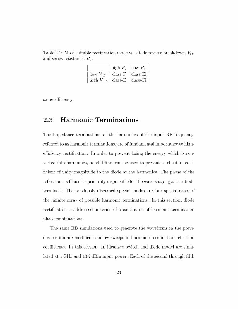
Table 2.1: Most suitable rectication mode vs. diode reverse breakdown, VrB
and series resistance, Rs.
high Rs low Rs
low VrB class-F class-Eihigh VrB class-E class-Fi
same efficiency.
2.3 Harmonic Terminations
The impedance terminations at the harmonics of the input RF frequency,
referred to as harmonic terminations, are of fundamental importance to high-
efficiency rectication. In order to prevent losing the energy which is con-
verted into harmonics, notch lters can be used to present a re ection coef-
cient of unity magnitude to the diode at the harmonics. The phase of the
re ection coefficient is primarily responsible for the wave-shaping at the diode
terminals. The previously discussed special modes are four special cases of
the innite array of possible harmonic terminations. In this section, diode
rectication is addressed in terms of a continuum of harmonic-termination
phase combinations.
The same HB simulations used to generate the waveforms in the previ-
ous section are modied to allow sweeps in harmonic termination re ection
coefficients. In this section, an idealized switch and diode model are simu-
lated at 1GHz and 13.2 dBm input power. Each of the second through fth
23

harmonics are terminated with a re ection coefficient of magnitude 0.92 and
variable phase. The second and fourth harmonics are stepped in increments
of 9 as the third and fth harmonic are swept every 9. The result is shown
as a plot of rectied voltage vs. even and odd harmonic termination phase
angle.
A fundamental impedance and load resistance between the optimal val-
ues of Zfund and RL for class-E and class-F are also chosen in each case.
This allows comparison of harmonic-termination response between these two
classes which does not depend on the termination of the fundamental. This
also means however that the class of operation is not optimal class-E or F
when the harmonics reach their class-E or F values.
2.3.1 Simulations Using an Exponential Switch
An idealized diode is created using the resistance given by Equation 2.4 in
parallel with a 0.10 pF capacitor and both in series with a resistance of 11Ω
(Cj and Rs for the MA4E2054). In this case there is no reverse breakdown
voltage and the diode is referred to here as an exponential switch. Therefore
the main source of loss is expected to be during current conduction through
the series resistance.
The results of Figure 2.7 show that optimal rectication performance
results for regions near the class-F and class-E terminations. This is due
to the near 180 current conduction angle and smooth transition of charge.
In the case of short-circuited even harmonics, the conduction angle becomes
24
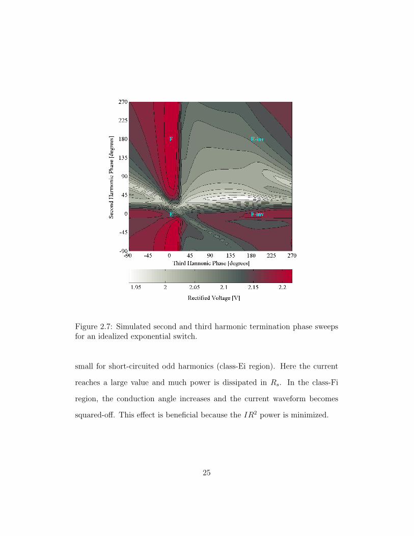
Figure 2.7: Simulated second and third harmonic termination phase sweepsfor an idealized exponential switch.
small for short-circuited odd harmonics (class-Ei region). Here the current
reaches a large value and much power is dissipated in Rs. In the class-Fi
region, the conduction angle increases and the current waveform becomes
squared-off. This effect is benecial because the IR2 power is minimized.
25

2.3.2 Simulations Using a Diode Model
Figure 2.8: Simulated second and third harmonic-termination phase sweepsfor the spice model of the diode.
The spice model for the MA4E2054 diode is simulated with the same
frequency and power as the exponential switch, but with slightly modied
fundamental input impedance for comparison purposes. In this case the
breakdown voltage of 5V becomes a large factor, as demonstrated by Fig-
26

ure 2.5 and Figure 2.6.
Figure 2.8 shows that the favored region is now purely the case where the
voltage is squared-off and kept below the breakdown voltage. Furthermore,
the low-conduction angle, high current peak case (class-Ei) actually becomes
much more favorable than class-E and class-Fi simply due to its low voltage
prole. A saddle point in rectied voltage occurs at class-E, while class-Fi
exhibits the poorest performance.
2.3.3 Measurements
A measurement set-up was created at dBm Engineering using a Focus impedance
tuner and 2nd and 3rd harmonic tuner (see Figure 2.14 below) to produce
measurements comparable to the previous simulation. The MA4E2954 diode
was placed in a test xture and measured at the same frequency and input
power level. The fundamental impedance tuner is used to vary the input
impedance as desired. A harmonic tuner was capable of presenting, on aver-
age, a 0.92 magnitude re ection coefficient at the second and third harmonics.
The phase is then variable to a precision better than a degree. The Focus
control software is able to adjust the fundamental impedance tuner as the
harmonic tuner changes so that the fundamental impedance is always the
same. However, the correction is limited and it is not guaranteed that a
particular fundamental impedance can be reached for every position of the
harmonic tuner without the use of pre-matching. In the present case, pre-
matching was not available. As a result, desired fundamental impedances
27

Figure 2.9: Measured second and third harmonic termination phase sweepsfor the MA4E2054 diode.
could not be reached for second harmonic phase angles in the rang of -15
to 15. Therefore the points on the measured phase sweep near class-E and
class-Fi (2nd harmonic phase = 0) are interpolated between -15 to 15. The
rest of the points are separated by 30 for the second harmonic and 30 for
the third harmonic.
The results are similar to those of the simulated diode model in Figure 2.8
28

in that the optimal regions occur near the class-F and Ei cases while the
poorest performance occurs along the class-E to Fi region.
2.4 Rectifier Source-Pulling
A source-pull measurement or simulation is the name given to the method of
sweeping the impedances seen by a device looking back towards the source.
As in the previous section, the phase of the harmonic impedances are varied
to nd optimal rectication performance, the source-pull allows the funda-
mental impedance to be varied for a particular set of harmonic terminations.
In this section, simulated load pulls are demonstrated for a large-signal case
to show how the optimal impedance, rectication efficiency, and re ected
power reacts to fundamental impedance.
2.4.1 Simulated Source Pulls for the Diode Model
The following gures show the resulting RFDC efficiency and normalized re-
ected power (Prefl(db)−Pin(dB)) at the fundamental versus source impedance.
In each case, the source impedance is varied using a single-stub matching
section as in Figure 2.4. In the following cases, however, the harmonic ter-
minations are maintained using the proper lengths of open transmission line.
The operating conditions for these simulations using the MA4E2054 diode
are f = 1GHz, Pin = 13:2 dBm, and RL = 300 Ω.
The voltage and current levels of the waveforms demonstrated in the
29

0.2 0.5 1 2
j0.2
−j0.2
0 ∞
j0.5
−j0.5
0 ∞
j1
−j1
0 ∞
j2
−j2
0 ∞
3040 50 60
70
0.2 0.5 1 2
j0.2
−j0.2
0 ∞
j0.5
−j0.5
0 ∞
j1
−j1
0 ∞
j2
−j2
0 ∞
−3
−6 −9 −12
(a) (b)
Figure 2.10: Class-F source-pull diagram of RFDC efficiency (a) and nor-malized rf re ected power (b).
0.2 0.5 1 2
j0.2
−j0.2
0 ∞
j0.5
−j0.5
0 ∞
j1
−j1
0 ∞
j2
−j2
0 ∞
20
10
3035
40
0.2 0.5 1 2
j0.2
−j0.2
0 ∞
j0.5
−j0.5
0 ∞
j1
−j1
0 ∞
j2
−j2
0 ∞
−3
−6
−9 −12
(a) (b)
Figure 2.11: Class-E source-pull diagram of RFDC efficiency (a) and nor-malized rf re ected power (b).
30

0.2 0.5 1 2
j0.2
−j0.2
0 ∞
j0.5
−j0.5
0 ∞
j1
−j1
0 ∞
j2
−j2
0 ∞
30
40 50
60
70 0.2 0.5 1 2
j0.2
−j0.2
0 ∞
j0.5
−j0.5
0 ∞
j1
−j1
0 ∞
j2
−j2
0 ∞
−3
−6 −9 −12
(a) (b)
Figure 2.12: Class-Ei source-pull diagram of RFDC efficiency (a) and nor-malized rf re ected power (b).
0.2 0.5 1 2
j0.2
−j0.2
0 ∞
j0.5
−j0.5
0 ∞
j1
−j1
0 ∞
j2
−j2
0 ∞
10
20
30
350.2 0.5 1 2
j0.2
−j0.2
0 ∞
j0.5
−j0.5
0 ∞
j1
−j1
0 ∞
j2
−j2
0 ∞
−3
−6−9 −12
(a) (b)
Figure 2.13: Class-Fi source-pull diagram of RFDC efficiency (a) and nor-malized rf re ected power (b).
31

previous section apply for these source-pull diagrams and help explain why
the class-E and Fi cases had poorer results. The reverse breakdown voltage
for these simulations was 5V and voltages in excess of this value are the
main contributors to loss and low efficiency. In fact, for class-E, the optimal
source impedance no longer corresponds to the class-E impedance, but simply
to where the diode is best matched in terms of re ection.
2.4.2 Measured Source Pulls
A source-pull measurement system was used on the MA4E2054 diode using
the same Focus Microwaves measurement system used for the harmonics
sweep in Section 2.4.2. The system includes an RF source, passive source-
impedance tuner, passive 2nd and 3rd harmonic tuner, and diode test xture
(Figure 2.14) courtesy of dBm Engineering.
Source-pull measurements were taken for several combinations of RL and
harmonic terminations. Graphical results of the class-E and class-F termi-
nated source-pulls are shown in Figure 2.15. The results for each of the
four classes are summarized in the next section and compared with simu-
lated values. The same operating conditions (fo,Pin,RL) were used in the
measurements as were used for the above simulated source-pulls.
32

Figure 2.14: Measurement set-up used for the diode source pull with funda-mental impedance tuner and second and third harmonic phase tuners. Laband equipment courtesy of dBm Engineering and Focus Microwaves.
2.5 Switched Mode Rectifier Performance
The performance of four switched-mode rectiers is summarized and com-
pared with simulated results for the MA4E2054 diode operating at 1GHz
with 13.2 dBm input power. Subsequently, four microstrip circuit designs
are presented as show how each class can be realized outside of the source-
pull system.
2.5.1 Comparison of Simulated and Measured Results
The results of the previous simulated source-pulls are summarized in Ta-
ble 2.2. For each class, the source impedance is chosen based on the optimal
rectication efficiency. Not shown in the table is the result of the matched
33

0.2 0.5 1 2
j0.2
−j0.2
0 ∞
j0.5
−j0.5
0 ∞
j1
−j1
0 ∞
j2
−j2
0 ∞
21
2733 37
39 41
27
35
Source Pull:
Efficiency contoursfor class−E terminations
0.2 0.5 1 2
j0.2
−j0.2
0 ∞
j0.5
−j0.5
0 ∞
j1
−j1
0 ∞
j2
−j2
0 ∞
39
39
47
51
5559
Source Pull:
Efficiency contoursfor class−F terminations
(a) (b)
Figure 2.15: Source-pull diagrams for Class-E (a) and class-F (b) terminateddiodes showing contours of constant RFDC efficiency.
diode with no harmonic terminations. By comparison, its simulated maxi-
mum efficiency was 49% with an optimal source impedance of 153 + j14 Ω.
Similarly, Table 2.3 shows the optimal source impedance for maximum rec-
tication efficiency for each class under the same operating conditions as
Table 2.2.
The discrepancies between the measured and simulated rectication ef-
ciencies are mostly due to the poor representation of actual reverse-bias
behavior given by the Spice model of the MA4E2054. A smaller effect can
be attributed to the non-ideal harmonic terminations of the measurement
system which led to extra loss in the circuit.
34
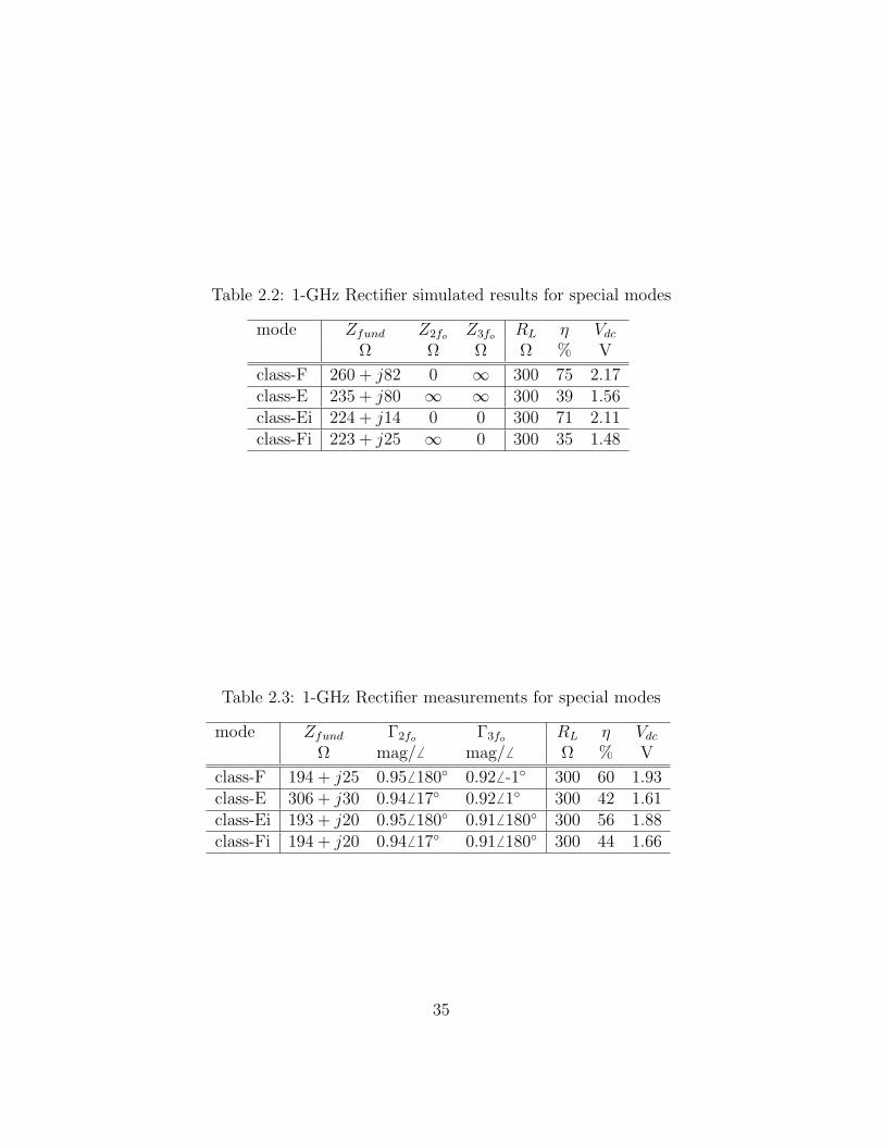
Table 2.2: 1-GHz Rectier simulated results for special modes
mode Zfund Z2fo Z3fo RL η Vdc
Ω Ω Ω Ω % V
class-F 260 + j82 0 1 300 75 2.17class-E 235 + j80 1 1 300 39 1.56class-Ei 224 + j14 0 0 300 71 2.11class-Fi 223 + j25 1 0 300 35 1.48
Table 2.3: 1-GHz Rectier measurements for special modes
mode Zfund 2fo 3fo RL η Vdc
Ω mag/ 6 mag/6 Ω % V
class-F 194 + j25 0.956 180 0.926 -1 300 60 1.93class-E 306 + j30 0.946 17 0.926 1 300 42 1.61class-Ei 193 + j20 0.956 180 0.916 180 300 56 1.88class-Fi 194 + j20 0.946 17 0.916 180 300 44 1.66
35

2.5.2 Circuit Designs for Switched Mode Rectifiers
Rectier designs are presented for each of the four classes of rectication
mentioned above. The transmission line scheme of terminating the harmonics
used in the simulations above are shown below for a putative microstrip
circuit. While the given electrical lengths of the open stubs provide exact
open and short circuits in simulation, the fringing capacitance and effective
propagation constant must be carefully taken into account in practice to
achieve the desired impedances at the harmonics. Microstrip implementation
should, however, provide greater accuracy than the source-pull system with
harmonic tuner.
The method used for fundamental-impedance matching used in the sim-
ulation was to use a pre-match single stub section followed by a ne-tuning
single stub section. In effect this comprised a double-stub matching section;
however, since single stub matching would be adequate, the fundamental-
impedance matching scheme is left as a block in Figure 2.16 and Figure 2.17.
Designing impedance matching circuits based on source-pull measure-
ments and method of moments simulations has been successfully carried out
and documented in [18] for power ampliers between 1 and 2GHz.
36

fundamentalmatching
short ckt for2nd harmonic
open ckt for3rd harmonic
~
50W
30o
30o
41o
45o
fundamentalmatching
short ckt for2nd harmonic
short ckt for3rd harmonic~
50W
30o
45o
(a) (b)
Figure 2.16: Class-F (a) and class-Ei (b) circuit layouts demonstrating pos-sible harmonic termination schemes in microstrip form. Line dimensions aregiven in electrical length referenced to the fundamental frequency.
fundamentalmatching
open ckt for2nd harmonic
open ckt for3rd harmonic
~
50W
30o
30o
8o
45o
fundamentalmatching
open ckt for2nd harmonic
short ckt for3rd harmonic
~
50W
30o15o
45o
(a) (b)
Figure 2.17: Class-F (a) and class-Ei (b) circuit layouts demonstrating pos-sible harmonic termination schemes in microstrip form. Line dimensions aregiven in electrical length referenced to the fundamental frequency.
37

Chapter 3
RF Energy Recycling:
A Broadband Rectenna Array
3.1 Introduction
Rectication of microwave signals for supplying dc power through wireless
transmission has been proposed and researched in the context of high power
beaming since the 1950s, a good review of which is given in [19]. In microwave
power transmission, the antennas have well-dened polarization and high rec-
tication efficiency enabled by single-frequency, high microwave power densi-
ties incident on an array of antennas and rectifying circuits. Applications for
this type of power transfer have been proposed for helicopter powering [19],
solar-powered satellite-to-ground transmission [8], inter-satellite power trans-
mission [20] including utility power satellites [21], mechanical actuators for
space-based telescopes [9], small dc motor driving [22], and short range wire-
less power transfer, e.g. between two parts of a satellite. Both linear [23],[24]
dual-linear [9],[25] and circular polarization [8], [26] of the receiving antennas
were used for demonstrations of efficiencies ranging from around 8590% at
lower microwave frequencies to around 60% at X-band and around 40% at
Ka-band [21].
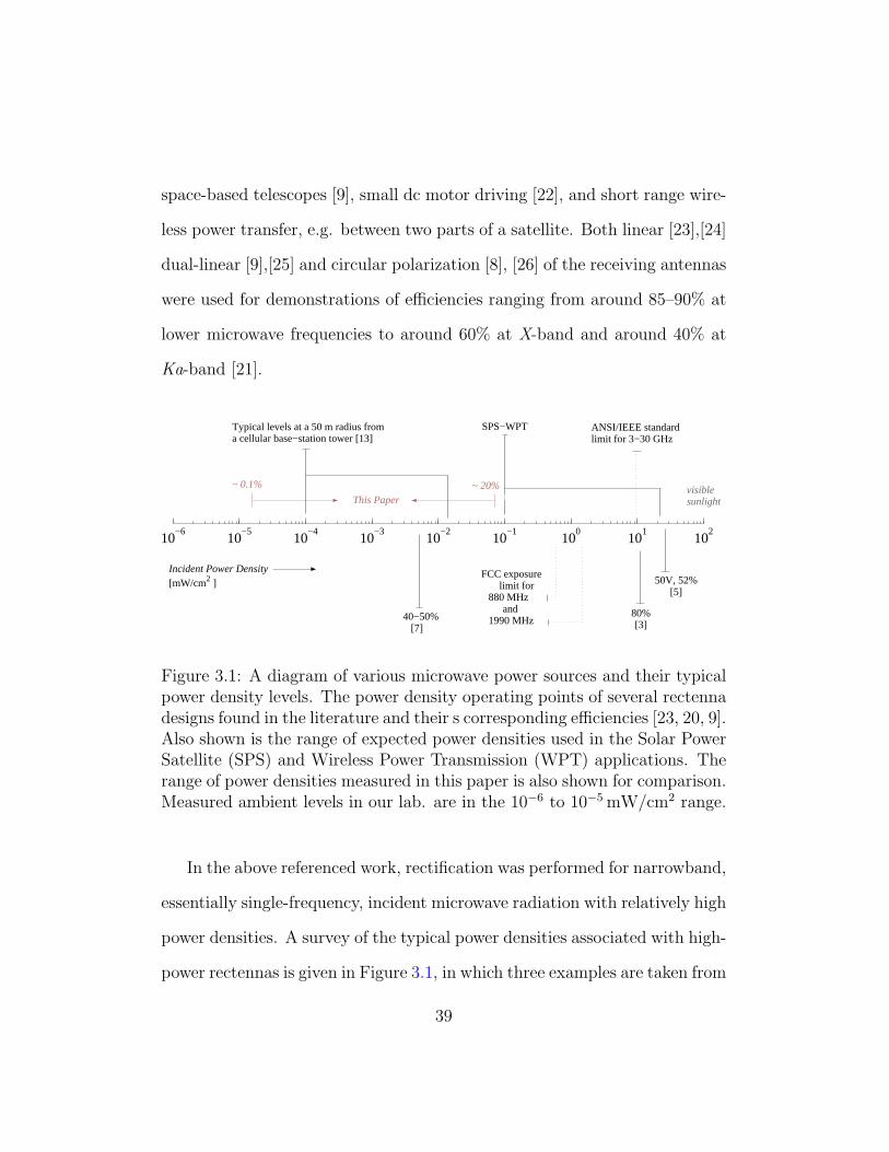
10−6
10−5
10−4
10−3
10−2
10−1
100
101
102
SPS−WPT
80%[3]
ANSI/IEEE standard limit for 3−30 GHz
visible sunlight
Incident Power Density [mW/cm2 ]
This Paper
Typical levels at a 50 m radius from a cellular base−station tower [13]
40−50%[7]
FCC exposurelimit for
880 MHz and
1990 MHz
50V, 52%[5]
~ 20%~ 0.1%
Figure 3.1: A diagram of various microwave power sources and their typicalpower density levels. The power density operating points of several rectennadesigns found in the literature and their s corresponding efficiencies [23, 20, 9].Also shown is the range of expected power densities used in the Solar PowerSatellite (SPS) and Wireless Power Transmission (WPT) applications. Therange of power densities measured in this paper is also shown for comparison.Measured ambient levels in our lab. are in the 10−6 to 10−5 mW/cm2 range.
In the above referenced work, rectication was performed for narrowband,
essentially single-frequency, incident microwave radiation with relatively high
power densities. A survey of the typical power densities associated with high-
power rectennas is given in Figure 3.1, in which three examples are taken from
39

[20],[9], and [23] along with the corresponding operating rectication efficien-
cies. Also shown in the gure are expected power densities near a typical
base station tower operating at 880 and 1990MHz [27]. Concerns have been
expressed in terms of possible health hazards [28]. In [23], rectication of low
power levels was discussed for battery-free transponders, with power densi-
ties on the order of 10−2 mW/cm2. More recently, broadband rectication of
very low-power incident radiation (less than 1mW/cm2) was demonstrated
in [29]. This paper focuses on incident power densities and input power levels
that are orders of magnitude lower than those associated with the projects
in the literature cited above.
In this paper, simulation, design and performance of a broadband rectenna
array (tested from 218GHz) for rectication of comparatively low-power
(10−5 to 10−1 mW/cm2), arbitrarily polarized incident radiation is presented.
The work is motivated by two types of applications: powering of low-power
sensor networks and rf energy recycling. Because of the low input power
levels, a nonlinear decrease in efficiency is expected when compared to power
beaming applications. The goal of this paper is to determine the usefulness
of low power rectication.
The general block-diagram of the rectenna array discussed in this paper
is shown in Figure 3.2. Multiple sources of different frequencies are radiating
power in all directions in a rich scattering environment. The DC powers from
many rectenna elements are added by current and voltage summing with a
40
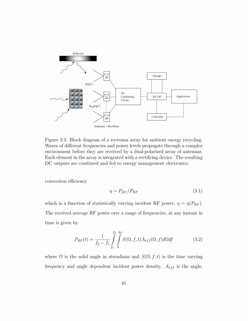
Storage
DC-DC Application
Controller
Antennas + Rectifiers
DCCombining Circuit
Reflector
S(Q,f)
Aeff(q,f)
Figure 3.2: Block diagram of a rectenna array for ambient energy recycling.Waves of different frequencies and power levels propogate through a complexenvironment before they are received by a dual-polarized array of antennas.Each element in the array is integrated with a rectifying device. The resultingDC outputs are combined and fed to energy management electronics.
conversion efficiency
η = PDC/PRF (3.1)
which is a function of statistically varying incident RF power, η = η(PRF ).
The received average RF power over a range of frequencies, at any instant in
time is given by
PRF (t) =1
f2 − f1
f2∫f1
4π∫0
S(Ω, f, t)Aeff (Ω, f)dΩdf (3.2)
where Ω is the solid angle in steradians and S(Ω, f, t) is the time varying
frequency and angle dependent incident power density. Aeff is the angle,
41

frequency, and polarization dependent effective area of the antenna. The DC
power at a single frequency, fi, is given by
PDC(fi) = PRF (t, fi)η[PRF (t, fi), ] (3.3)
where represents the diode mismatch to the antenna. Because of the nonlin-
earity of the diode, the mismatch is dependent on power as well as frequency.
The issues related to low-power arbitrarily-polarized reception, rectica-
tion and power management are addressed in this paper as follows:
Section 3.2 discusses rectication of low power microwave signals. Non-
linear simulations of the rectifying device are conrmed with source-pull
measurements over a broad frequency range and broad range of input
powers. The result is a range of RF impedances presented to the diode
for optimal rectication efficiency.
Section 3.3 discusses design of an antenna integrated with a rectier.
Electromagnetic eld simulations are coupled to nonlinear circuit sim-
ulations to ensure optimal broadband match between the antenna and
rectier. Based on known range of input power levels, a rectier diode
is chosen among several candidates. Measurements on single antenna
elements are compared to analysis results.
Section 3.4 describes the design and characterization of a 64element
dual circular polarized rectenna array. The frequency response, receive
radiation patterns, DC power rectication efficiency, and radiated har-
monics are measured. Finally, given the statistical nature of incident RF
42

radiation, the DC rectied power was measured over 10,000 trials with
varying frequency and power.
Section 3.5 presents a discussion on storage and management of the ex-
tracted DC power with two example applications.
3.2 Microwave Rectification and the Rectenna
At low RF frequencies (kHz to low MHz), both pn-diodes and transistors are
used as rectiers. At microwaves (1GHz and higher), Schottky diodes (GaAs
or Si) with shorter transit times are required. In the present case, we have
chosen silicon based on availability, low-cost, and simulated performance.
Similar to low-frequency, high-power applications, the diode is driven as a
half-wave rectier with an efficiency limited to
ηmax =1
1 + VD
2Vout
(3.4)
where Vout is the output DC voltage and VD is the drop across the conducting
diode. In this work it is more appropriate to measure the efficiency dened
by Equation 3.1 which includes the loss due to re ected power.
For low power applications, as is the case for collected ambient energy,
there is generally not enough power to drive the diode in a high efficiency
mode. Furthermore, rectication over multiple octaves requires a different
approach from standard matching techniques. In a rectenna application,
43

the antenna itself can be used as the matching mechanism instead of using
a transmission-line matching circuit as in [21][26]. The antenna design is
therefore heavily dependent on the diode characteristics. The following sec-
tion presents various techniques for analyzing diode operation at microwave
frequencies. The results are then used to design the antenna and integrated
rectenna for relevant ambient power levels.
3.2.1 Analysis and Design Method
A useful time domain analysis has been applied by McSpadden et al. in a
number of papers dealing with single-frequency rectennas at microwave fre-
quencies up to Ka-band [21]. The method uses current/voltage properties
of the diode as a basis for predicting rectied power levels and conversion
efficiencies. The method has proved a successful predictor of conversion ef-
ciencies over a broad range of incident power levels and load impedances.
In general this approach has been used for well ltered, well matched diodes
integrated with antennas for narrowband use.
Several properties of the diode at microwave frequencies require a more
comprehensive frequency domain approach: (1) The nonlinear capacitance
of the diode needs to be taken into account past a few GHz for most devices.
(2) Re ected harmonic energy from the source or load side of the diode can
alter the voltage across the diode. (3) The diode also begins to bias itself as
it produces more DC current, thus moving the DC operating point of the IV
curve in a nonlinear fashion.
44

Certain qualities of microwave rectication can be visualized best in the
time domain, i.e. monitoring the complex waveform across the diode. In the
frequency domain, the Harmonic Balance (HB) method of analysis presents a
more comprehensive treatment of the multi-spectral diode problem. Though
less helpful diagnostically and heavily dependent on the accuracy of the non-
linear model of the diode, HB provides a tool for addressing all previously
mentioned aspects of microwave rectication. The method intrinsically takes
into account the DC component and a specied number of harmonics, while
allowing the ability to specify the source impedance and harmonic termina-
tions.
3.2.2 Diode Source-Pull
A source pull of the diode is a sweep of RF input source impedance values
over a given area of the Smith chart. Figure 3.3 (a) shows the HB simula-
tion approach using Agilent ADS as well as the measurement approach using
impedance tuners. In both simulation and measurements, for a variety of in-
put powers the resulting DC voltage is quantied for each source impedance
and plotted on the Smith chart as shown in Figure 3.4. The region of op-
timal source impedance is later used for optimizing the antenna design so
that the antenna presents an equivalent source impedance to the diode. In
the simulation an assumption must be made for the impedance seen by the
re ected harmonics, and in the presented case this impedance was set to the
impedance of a broadband, self-complementary antenna, 189Ω.
45

Zs
~
dc-block
RL
dc-feed dc-probe
dio
de m
odel
rf- source
dc-lo
ad
(a)
50 V
~
RL
dc-feed dc-probe
dc-lo
ad
rf-source
impedance tuner
test fixtu
re
(b)
Figure 3.3: Circuit diagram of the Harmonic Balance simulation (a) anddiagram of the equivalent source-pull measurement setup (b).
Figure 3.4 demonstrates the range of optimal source impedances across
the range of 1 to 16GHz and -30 to 10 dBm input power. The magnitude
of the optimal source impedance becomes smaller with increasing incident
power. The same occurs as the DC load approaches the optimal value, how-
ever the effect is not as dramatic. More signicantly, the optimal source
impedance moves counter-clockwise along a constant admittance circle with
increasing frequency due to the junction capacitance.
The Smith chart plots of Figure 3.5 show a comparison between a simu-
46

0.2 0.5 1 2
j0.2
−j0.2
0 ∞
j0.5
−j0.5
0 ∞
j1
−j1
0 ∞
j2
−j2
0 ∞
Incr. finc
Incr. Pin
Incr. Pin
A B
C
D
Figure 3.4: Simulated range of optimal source impedances for the SMS7630Schottky diode as the frequency (finc) and input power (Pin) are varied.Within the shaded area, region A corresponds to high input power and lowfrequency, region B corresponds to low power and low frequency, etc.
lated source-pull using HB and measurements using a source-pull/load-pull
measurement system. A Focus 9-GHz coaxial tuner was used in the mea-
surement setup as described in Figure 3.3 (b).
3.3 Broadband Rectenna Design
Given the good agreement between simulation and experiment, HB was used
to evaluate several diodes. The rectication performance is seen to depend
most signicantly on saturation current, junction capacitance, built-in po-
47

0.2 0.5 1 2
j0.2
−j0.2
0 ∞
j0.5
−j0.5
0 ∞
j1
−j1
0 ∞
j2
−j2
0 ∞0.
4 V
0.48
0.56
0.64
MeasuredSource Pull
0.2 0.5 1 2
j0.2
−j0.2
0 ∞
j0.5
−j0.5
0 ∞
j1
−j1
0 ∞
j2
−j2
0 ∞
0.4
V
0.48 0.5
6
0.64
0.667
SimulatedSource Pull
(a) (b)
Figure 3.5: Measured (a) and simulated (b) source-pull of the MA4E2054diode at 1GHz. The contours show constant levels of DC voltage over sourceimpedance with constant RF input power.
tential, and series resistance. Figure 3.6 shows qualitatively the efficiency
performance of three different Schottky diodes obtained by HB simulations.
Based on these results the Alpha Industries SMS7630-079 zero-bias device
was selected.
3.3.1 Integrated Rectenna Analysis
In most rectenna designs the narrowband antenna is used to feed a trans-
mission line followed by space-consuming, traditional matching and ltering
sections. In contrast, in the work presented here the diode is integrated di-
rectly into the antenna. Consequently, the antenna is called upon to provide
48

1 3 5 7 9 11 13 15−20
−15
−10
−5
0
5
10
Frequency [GHz]
Inpu
t RF
Pow
er [d
Bm
]
MaCom − MA4E2054
Alpha − SMS7630
Is = 5E−6 A R
s = 20 Ω
Vj = 0.34 V C
j=0.24 pF
Alpha − SMS1546
Is = 3E−7 A R
s = 4 Ω
Vj = 0.51 V C
j=0.38 pF
Is = 3E−8 A R
s = 11 Ω
Vj = 0.4 V C
j=0.1 pF
Figure 3.6: Simulated qualitative comparison for three commercially avail-able diodes. This plot shows which diode will have optimal efficiency for agiven power and frequency. For the low power region, the Alpha SMS7630performs best over the frequency range.
both matching and ltering of the output signal, reducing the required area
and increasing the bandwidth. The antenna is included in the HB simulation
as the internal impedance of the power source used to drive the circuit. This
Thevenin equivalent model allows use of measured or simulated S-parameters
in the rectenna simulation Figure 3.3 (a).
3.3.2 The Spiral Antenna
As seen in the previous section, the major problem in broadband rectenna
design lies in the nature of the antenna and diode frequency dependent
49

mm
19 mm
1.5 mm
0.2
5m
m
1.5 mm
AlphaSMS7630-07923
Figure 3.7: Layout of the spiral antenna element with a packaged Schottkydiode connected directly at the feed. The size of the package limits the upperfrequency for this broadband antenna, while the overall size limits the lowfrequency limit.
impedance. For maximal power transfer, the antenna impedance would
match the optimal diode impedance for all frequencies. Our approach is to
present a constant impedance to the diode by using a frequency independent
antenna element.
The equiangular spiral is chosen for its convenient feed point where the
diode can be connected. A spiral with dimensions shown in Figure 3.7 was
designed using full wave MoM simulations with Ansoft Ensemble and Zeland
IE3D and has a measured frequency response shown in the Figure 3.8 (a).
The following measurements characterize the extent to which this spiral
rectenna achieves favorable rectication over a multi-octave band.
Figure 3.8 (b) shows the frequency dependence of the rectied voltage for
50

0.2 0.5 1 2
j0.2
−j0.2
0 ∞
j0.5
−j0.5
0 ∞
j1
−j1
0 ∞
j2
−j2
0 ∞
2 GHz
3 GHz
4 GHz
5 GHz
6 GHz
7 GHz
8 GHz
2 3 4 5 6 7 80
0.05
0.1
0.15
0.2
0.25
0.3
0.35
Frequency [GHz]
DC
Vol
tage
[V
]
Measured
2 3 4 5 6 7 80
0.05
0.1
0.15
0.2
0.25
0.3
0.35
Simulated
SpiralAntenna
(a) (b)
Figure 3.8: (a) Simulated S-parameters of the spiral antenna along with op-timal diode source impedance from 2 to 8GHz. (b) Resulting HB simulationand measurements of the DC rectied voltage response across a 600Ω load.
approximately 0 dBm input to the diode. The disagreement at around 4GHz
is beleived to be caused by a resonance in the unbalanced coaxial feed. There-
fore, an idependent validation for the simulation method was performed on
a well characterized Vivaldi tapered slot antenna with a balanced antipodal
feed [30]. In this case the nonlinear simulation and measured performance
agree closely (Figure 3.9).
51
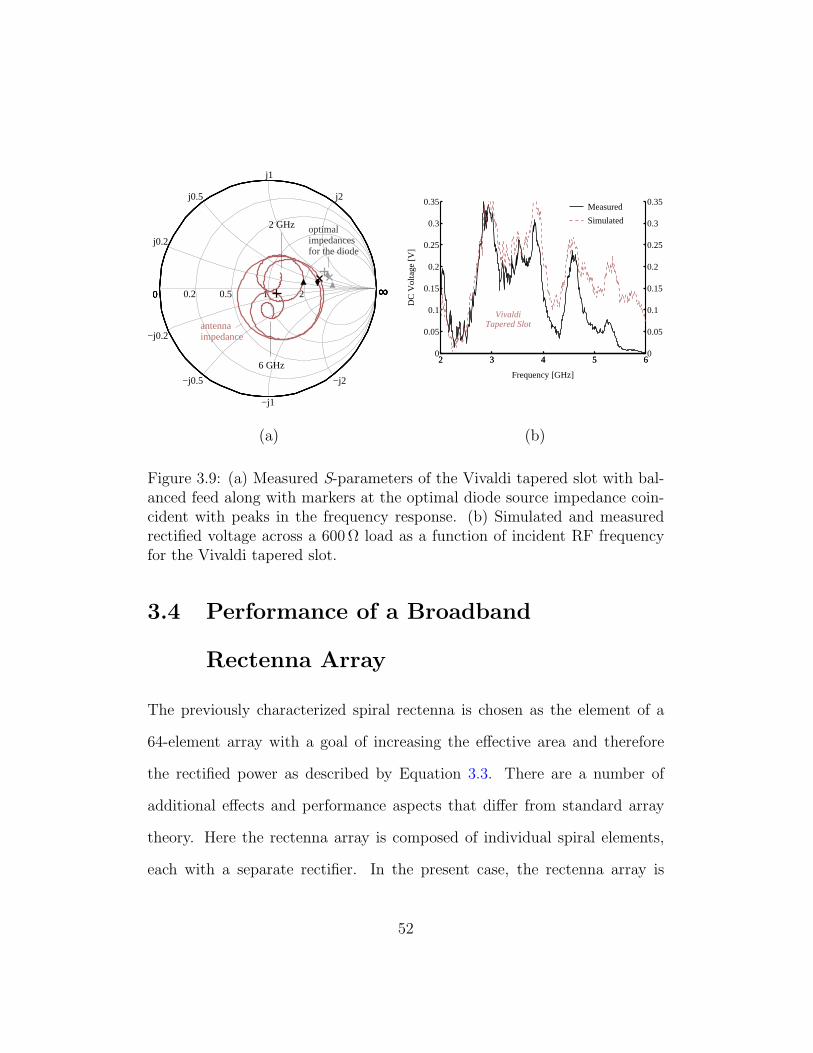
0.2 0.5 1 2
j0.2
−j0.2
0 ∞
j0.5
−j0.5
0 ∞
j1
−j1
0 ∞
j2
−j2
0 ∞
2 GHz
6 GHz
antennaimpedance
optimalimpedances for the diode
2 3 4 5 60
0.05
0.1
0.15
0.2
0.25
0.3
0.35
Frequency [GHz]
DC
Vol
tage
[V
]
Measured
2 3 4 5 60
0.05
0.1
0.15
0.2
0.25
0.3
0.35
Simulated
VivaldiTapered Slot
(a) (b)
Figure 3.9: (a) Measured S-parameters of the Vivaldi tapered slot with bal-anced feed along with markers at the optimal diode source impedance coin-cident with peaks in the frequency response. (b) Simulated and measuredrectied voltage across a 600Ω load as a function of incident RF frequencyfor the Vivaldi tapered slot.
3.4 Performance of a Broadband
Rectenna Array
The previously characterized spiral rectenna is chosen as the element of a
64-element array with a goal of increasing the effective area and therefore
the rectied power as described by Equation 3.3. There are a number of
additional effects and performance aspects that differ from standard array
theory. Here the rectenna array is composed of individual spiral elements,
each with a separate rectier. In the present case, the rectenna array is
52

composed of individual spiral elements, each independent rectiers. The
fundamental property of such an array is that the energy is rectied at each
element, and the DC voltages are subsequently combined. The radiation
pattern for a single element at a single frequency incident wave measured at
DC can be dened as
GDC(, ) = η(PRF )4 PRF
S(, )2= η(PRF )G(, ) (3.5)
where G(, ) is the RF radiation pattern. The DC radiation pattern, GDC ,
is different from the RF radiation pattern due to the nonlinear dependence
of efficiency on RF power. The resulting pattern obtained by measuring the
DC voltage across an optimal load exhibits lower gain at larger angles and
. The radiation pattern for the n-element array is given by
GnDC(, ) = (PRF )GDC(, ) (3.6)
where is a function of incident RF power and DC combining circuit. To
rst order, is not a funtion of incidence angle.
3.4.1 Array Design
Figure 3.10 depicts the compact element spacing. At lower frequencies the
increased mutual coupling between elements and the presence of the bias
lines increases the power delivered to the diodes by effectively increasing
the effective aperture of each element. The problem of polarization perfor-
mance is addressed by alternating left and right circular polarization between
53

neighboring elements, and by an additional rotation by 90 from element to
element. This means that the array suffers an average 3 dB input polariza-
tion loss for every possible polarization of the incident energy. However, this
strategy ensures a at polarization response.
Figure 3.10: Diagram of the 64-element array. Received RF power is rectiedat each spiral locally and the combined DC power for all elements is extractedusing two bias lines at the edges of the array (not shown). A number ofpossible DC connections and their effect on efficiency are described in thetext.
54

The crucial design step for the array is to acheive optimal DC combin-
ing efficiency. Previous work shows that predominately parallel connections
(current-summing) lead to smaller matched loads for the rectenna [31]. For a
series connected array (voltage-summed), the matched load is much higher.
This can be seen by reducing the array to a combination of DC Thevenin
sources where the matched load corresponds to the total source resistance.
The nonlinear performance of the diodes must again be considered when con-
sidering the DC connections. Increased current or voltage in a predominately
series or parallel-connected array can lead to over-biasing of the individual
diodes such that the rectication process is uniformly degraded over the ar-
ray. Furthermore, the DC power level is very sensitive to under illumination.
For these reasons, the 64 element array was connected using 2 1 parallel
pairs connected in series to form a 2 2 sub-subarray: four of these are
connected in parallel to create a 4 4 subarray: four more of these are then
left as units to comprise the 8 8 array with recongurable connectivity.
3.4.2 Frequency Response
The frequency dependence is measured in two ways: three-dimensional pat-
terns are integrated from 2 to 8GHz where sufficient power was available for
the measurement. Since the radiation patterns are reasonably smooth, only
the broadside frequency response was measured. Higher input powers were
used for 2 to 8GHz and a low power level was used for the broad range from
2 to 18GHz. The broadside frequency response was also measured using a
55

uniform incident power density to synthesize constant input power to the
diodes. The results for three input power levels are shown in Figure 3.11.
2 4 6 8 10 12 14 16 18−60
−50
−40
−30
−20
−10
0
10
Frequency [GHz]
DC
Rec
tifie
d P
ower
[dB
m]
2 4 6 8 10 12 14 16 18−60
−50
−40
−30
−20
−10
0
10
Pr / G
r = 17.5 dBm
Pr / G
r = 7.5 dBm
Pr / G
r = −15.5 dBm
ambient
Figure 3.11: Measured broadband frequency response for various incidentpower levels related to the power density, S, by Pr/Gr = S2/(4). Theshaded area represents the range of rectied power levels resulting from am-bient RF background signal present in the building.
3.4.3 DC-Power Response and Radiated Harmonics
To gain a better understanding of the nonlinear power dependence of the
rectenna, a sweep of the input power is performed and the resulting DC
output and reradiated power is quantied (Figure 3.12). The measurement
is made with broadside linearly polarized radiation at 3GHz with incident
power densities ranging from tens of nW/cm2 to 0.1 mW/cm2. The reradi-
ated energy is measured with a second antenna placed at broadside on the
56

Table 3.1: Rectication efficiency for a 22 sub-array and the 88 arraywith three DC-connection schemes for a low and high incident power density.Quartiles are dened as the 44 subarrays.
22 88 88 88
power density 2 in series, 2 in series, quartiles quartiles[mW/cm2] 2 in parallel 2 in parallel all in parallel all in series
S = 6:2 10−2 0.4% 16% 20% 13%
S = 6:2 10−4 0.03% 1.1% 2.3% 0.95%
opposite side of the rectenna. The DC is extracted with bias lines and mea-
sured across a 100Ω load. The rectication efficiency reaches the 20% range
for an incident power density of 0.1 mW/cm2 and arbitrary polarization.
Also shown in the plot is the relative amount of re ected power along with
the radiated power of the 2nd through 5th harmonics. The re ected power is
found from a time-gated S11 measurement using a vector network analyzer.
The result, consistent with simulation results, indicates that the re ected
varies linearly with input power up to 0.1mW/cm2. Simulations suggest,
however, that the re ections begin to drop as higher power levels are applied
(as more incident power becomes converted to DC and harmonics).
For different DC connections the diodes across the array are biased at dif-
ferent quiescent points on the diode IV curve. Table 3.1 shows efficiency mea-
sured across a 600Ω load for a 22 sub-array and the 88 array with three
DC-connection schemes for a low and high incident power density. Quartiles
57

are dened as the 44 subarrays. For this array the parallel conguration
of the subarrays gave the highest efficiency over the range of incident power
densities.
10−4
10−3
10−2
10−1
−50
−40
−30
−20
−10
0
10
20
Incident Power Density [mW/cm2]
Pow
er [
dBm
]
10−4
10−3
10−2
10−1
−50
−40
−30
−20
−10
0
10
20
2nd
3rd
4th 5t
hDC
reflected
incident power
Figure 3.12: Measured re ected, rectied, and reradiated harmonic power asa function of incident power density. The measurement was performed at3.4GHz.
3.4.4 DC Receive Patterns and Polarization
The radiation patterns of the rectenna array are found by measuring the
output DC rectied power over a hemisphere sampled at 1012 points, Fig-
ure 3.14 (a) and Figure 3.14 (b). These patterns are a superposition of the
response to two orhtogonally linearly polarized incident waves. At higher
frequencies the spiral element is predominately circularly polarized. In order
58
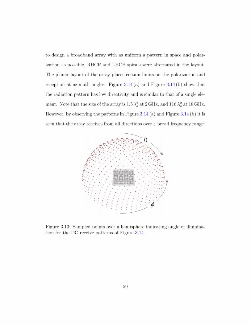
to design a broadband array with as uniform a pattern in space and polar-
ization as possible, RHCP and LHCP spirals were alternated in the layout.
The planar layout of the array places certain limits on the polarization and
reception at azimuth angles. Figure 3.14 (a) and Figure 3.14 (b) show that
the radiation pattern has low directivity and is similar to that of a single ele-
ment. Note that the size of the array is 1.52o at 2GHz, and 1162
o at 18GHz.
However, by observing the patterns in Figure 3.14 (a) and Figure 3.14 (b) it is
seen that the array receives from all directions over a broad frequency range.
Figure 3.13: Sampled points over a hemisphere indicating angle of illumina-tion for the DC receive patterns of Figure 3.14.
59

(a) (b)
Figure 3.14: Measured DC Power as a function of angle of incidence over ahemisphere for two orthogonally linearly polarized input waves at 2GHz, (a),and 4.6GHz, (b). The pattern is related to an RF radiation pattern throughEquation 3.5 and Equation 3.6.
3.4.5 A Statistical Study of Multitone Performance
As a nal test, the array is placed in a controlled, multitone environment.
The point of this test is to demonstrate how the DC response improves or
degrades when more waves of more than one frequency are incident simul-
taneously. Two signal sources, separated by 20 in incidence angle from the
rectenna and 45 in polarization, are used to represent multiple inputs with
variable frequency and power. In order to ensure uncorrelated input waves,
paired frequencies and power levels are generated randomly with a uniform
60

distribution using Matlab.
The experiment is run by rst generating one randomized frequency be-
tween 2 and 8GHz and one incident power level between approximately
0.1W/cm2 and 0.1mW/cm2. Each source is turned on separately to record
the independent DC rectied powers. Both sources are then turned on simul-
taneously and the new rectied power recorded. This process is repeated for
10,000 randomized input pairs. The sums of the two independent rectied
powers for each trial were then sorted and compared with the corresponding
rectied power from the simulataneous illumination from both sources.
0 2000 4000 6000 8000 10000−30
−25
−20
−15
−10
−5
0
DC
Rec
tifie
d P
ower
[dB
m]
0 2000 4000 6000 8000 10000−30
−25
−20
−15
−10
−5
0
Trials
mean increase: × 1.61
1.41
1.28
Simulataneous illumination
Independent illumination
Figure 3.15: Comparison of total recitied power for independent and si-multaneous dual-frequency illumination as explained in Section 4 E. Theresults of 10,000 trials are rank-ordered by DC power to illustrate the powerdependent increase in rectication efficiency.
The result (Figure 3.15) reveals the phenomenon that the independent
61

sources combine nonlinearly, when simulataneously incident, to produce more
rectied power in every instance. The amount of power increase (Psimul/Pindep)
when both sources are on correlates roughly with the amount of rectied
power when both sources are off. This correlation is much stronger than the
frequency or incident power correlation. For this reason, Figure 3.15 was
plotted according to Pindep. Also shown is the mean increase in power for
three portions of the curve.
It should also be noted that in general, the power-increase diminishes as
the two frequencies approach one another. Furthermore, local power-increase
minima occur for certain difference frequencies, i.e. jf j. This is thought to
be due to a spiral input impedance which efficiently radiates the difference
frequency rather than further rectifying the energy. A map of simultaneous
illumination power increase is show in Figure 3.16 for frequencies over 2 to
8 GHz with constant Pr/Gr.
3.5 Energy Storage and Management for Low
Power Applications
To summarize, a study of rectication of broadband statistically-varying rf
radiation is presented in this paper. The experimental results show that
the combined electromagnetic eld analysis for the radiating element and
harmonic balance nonlinear circuit simulations result in predictable rectenna
performance. The work focuses on arbitrary polarized low incident power
62

Figure 3.16: Psuedocolor representation of the power increase of simultane-ous illumination over the independently summed case. In this plot, the xand y-axis represent the frequency of each of the two transmitters while thePr/Gr ration for each was kept constant.
density reception and rectication and shows that rectication efficiencies
with average 20% over time, frequency and polarization are achieved. If
one of these requirements is relaxed, i.e., high-power, narrowband, linearly-
polarized and/or time-constant power is transmitted, higher efficiencies up
to 60% at X-band [21] can be expected. The motivation for considering
63

the low-power random case are applications in ambient energy recycling and
low-power batteryless sensors.
The rst type of application addresses using otherwise wasted power,
which in some cases can also help reduce health hazards. For example, the
rooftops of buildings in city centers are often leased to a number of wireless
providers and technical staff has reported health problems when servicing
a transmitter in the presense of other operating transmitters [29]. In this
environment, a variety of output powers, frequencies, and polarizations are
present, and interference between a number of antennas in each other's near
elds changes their radiation properties, accounting for more wasted power.
The results of this paper show that this power can be absorbed (received),
rectied and stored for future use.
Figure 3.1 shows the more typical levels of ambient power densities in
the microwave frequency range, with power levels that are too low for most
continuous electronic functions. However, if this energy is stored over time
efficiently, realistic functions can be performed in discrete time intervals.
The ambient rf power levels vary by several orders of magnitude, implying
a varying DC load as re ected in the IV characteristics of a single rectenna
element, shown in Figure 3.17. For maximum DC power generation, it is
necessary to either match the output characteristics of the source with the
load, or to insert an intermediate dc-dc converter with peak power tracking.
Many techniques for low-power dc-dc conversion are described in [33], with an
emphasis on pulse-width modulated (PWM) converters. Traditional PWM
64

converters are likely to consume far too much power in the control and gate
drive circuitry and/or require large off-chip inductor(s) for low-frequency op-
eration. As an alternative, switched-capacitor (SC) converters can provide
high efficiency conversion at low power levels over a discrete range of con-
version ratios determined by the circuit size and complexity [34]. Although
parasitics in silicon processing have limited efficiency of SC converters, recent
advances in technologies such as fully-depleted silicon-on-insulator (FD-SOI)
have enabled fully integrated efficiencies of greater than 90% [35].
10−6
10−5
10−4
10−3
10−2
10−1
100
10−9
10−8
10−7
10−6
10−5
10−4
10−3
10−2
Voltage [V]
Cur
rent
[A
]
Pin
= −40 dBm
63 kΩ
−30 dBm
−20 dBm
63 kΩ
4 kΩ
630 Ω
250 Ω
100 Ω
−10 dBm
0 dBm
10 dBm
Figure 3.17: Simulated IV-curves as a function of load resistance and inputRF power to the diode. The peaks in rectied power are indicated by circleswith the corresponding optimal load resistance.
Referring to the block diagram in Figure 3.2, two options for energy stor-
age include capacitors and micro-batteries [36]. Capacitive energy storage is
appropriate for applications where repeated functions of storing and utilizing
65

small energy packets is performed, using on-chip (up to 10's of pJ of off-chip,
up to 10's of J) capacitors. For prolonged operation or larger energy pack-
ets, up to four orders of magnitude higher energy densities can be achieved
using microbatteries [37].
To illustrate the application of the rectenna energy source, we consider
the ability to generate 10J energy packets, which is sufficient for a 1mW,
10s load operation. The energy packet size was selected arbitrarily, but
could be used for example for RF transmission of up to 10 kbit data packets,
or simple sensory and signal processing functions. Over the range of incident
power densities under consideration Figure 3.1, and assuming
A = Aeff = 25 cm2 (3.7)
array, we estimate incident power levels of
PRFmin = 250 nW, PRFmax = 2:5 mW: (3.8)
Assuming a DC-DC conversion efficiency of 90% and rectication efficiencies
of
η(PRFmin) = 1%, η(PRFmax) = 20%: (3.9)
an average DC power output is obtained as
PDCmin = 2nW, PDCmax = 450W: (3.10)
The above estimated power levels can be recycled using this kind of a
device. In another important application, batteryless sensors, this power is
66

used to transmit power from this sensor. There are two possible scenarios:
(1) vary integration time to achieve xed energy level, or (2) x integration
time and vary energy packet level. Following approach (1), the system would
be capable of a xed 10J operation at discrete intervals varying from 1.4
hours in the worst case to 20ms in the best case. Thus if a simple sensor
required one energy packet to perform the sensory function, and one packet
to transmit data, it would be able to transmit new data around 20 times per
second in the best case.
An example of this application is a manufacturing environment, where a
large number of sensors occasionally transmit data such as stress, tempera-
ture, pressure, etc. A large number of such sensors with no batteries that
need replacing (or recycling) can be charged with a low-power transmitter
overnight. In such an indoor multipath propagation environment, the spatial
distribution of polarization and power varies statistically [38]. The results of
this paper show that it is possible to efficiently collect such energy by receiv-
ing and rectifying two orthogonal polarizations independently and adding
the power upon rectication.
67

Chapter 4
DC–RF Conversion:
Microwave Oscillators
A design methodology for a high-efficiency, switched mode oscillators is pre-
sented in the context of present high frequency oscillators and switched mode
ampliers. This chapter seeks to provide the framework for a class-E X-
band oscillator with maximized DCRF efficiency without regard to circuit
size, complexity, or phase-noise performance. Instead this chapter focuses
on a measurement-based nonlinear design methodology for acheiving class-E
performance. An external feedback topology is used in order to be able to
compare the oscillator performance to well documented class-E amplier per-
formance. The goal is that future class-E oscillators using different devices or
topologies can be designed and evaluated based on the methods and results
of this work.

4.1 Microwave Oscillators
Present day power oscillators are used mostly for communication and radar
systems [1]. These are typically made with Si BJTs, MESFETs, IMPATT
diodes, or GUNN diodes depending on the frequency of operation, noise
requirements, or desired output power. Microwave signals generated for fre-
quency and phase purity are typically multiplied up from a MHz range crystal
oscillator. Some oscillator needs require octave, or better, tuning in the mi-
crowave range. In each of these cases, power, signal purity, and tunability
are one or more of the primary concerns and each comes at the expense of
the DCRF efficiency.
Transistor power oscillators have been implemented in planar circuits
with some form of feedback mechanism. Feedback is necessary to make the
transistor unstable, unlike two-terminal devices. Series feedback has been
implemented with open lengths of transmission lines, utilizing the internal
feed-back of the transistor; Parallel feedback can be used to directly connect
two of the terminals RF-wise; Resistive feedback using lumped components
is also commonly used as with the Colpitts and Clapp-Gouriet models [39, 1].
These types of oscillators are usually run in large signal mode and operate
with compressed gain of the device. This helps achieve the maximum amount
of output power from the device as well as lower amplitude noise. Improved
phase noise in power oscillators is usually accomplished by increasing the Q
of the circuit, typically by using a dielectric resonator, or phase locking to
69

a cleaner signal. The selection of the nonlinear device particularly affects
the low-frequency phase noise characteristics. For instance, silicon devices
have signicantly lower icker noise than GaAs devices and therefore exhibit
superior phase noise performance [40].
In energy conversion applications, the DCRF conversion efficiency be-
comes more important to the designer, but not at the expense output power
which should remain high. DCDC conversion typically uses a switched or
pulse modulated oscillator to regulate a DC power source. In most cases the
oscillator or pulse generator is desired to be a near lossless circuit element
so that the DC-DC conversion is as efficient as possible. DC-DC conver-
sion at microwave switching speeds is now receiving attention in applications
ranging from low-transient voltage regulation [7] to satellite-to-earth power
beaming [8]. In these cases phase noise and tunability are not important
because usually only one frequency is of interest and it is not used as a signal
carrier.
In another example, wireless devices can benet from improved DCRF
conversion efficiency. In general, a higher oscillation efficiency leads to a
longer battery lifetime. Furthermore, some applications may impose strict
requirements on power consumption of the signal generator. Again, how-
ever, such requirements on the efficiency will put a strain on the achievable
phase noise, tunability, and size, and therefore this trade-off must always be
considered.
It is with this high-efficiency angle in mind that a class-E oscillator is
70

Table 4.1: Solid-state device selection based on output power and microwavefrequency [1].
Device Frequency Corresponding CorrespondingRange: Max Pout: Max PAE:
Si BJT 15GHz 50020W > 60%GaAs MESFET 525GHz 305W 6040%IMPATT 25200GHz 5W30mW < 15%(GUNN) 25150GHz 1W1mW
considered in this chapter. This focus limits the types of circuits to be con-
sidered. For instance the Colpitts and Clapp-Gouriet models suffer from too
much loss in resistive elements to be be used in a high-efficiency design. A
series feedback design is desirable for its simplicity, but provides less control
over feedback level and class-E performance. The parallel feedback topology
allows direct implementation of existing class-E amplier topologies into the
oscillator. Therefore, this circuit method is the main focus of this chapter.
The following sections will discuss high efficiency class-E operation, meth-
ods for designing with this highly nonlinear mode, and a characterization
of what to expect from a class-E oscillator in terms of output power and
efficiency. Experimental results are given for a low-Q design and extensive
considerations and design guidelines are posited for a higher-Q design.
71

4.2 Class-E Operation
The advantage of operating the active device in an oscillator in class-E mode
lies in improved DCRF efficiency and consequent increased battery lifetime.
Using a switched mode of operation can have several drawbacks including in-
creased phase noise, AMPM conversion, and reduced tunability. In general,
the output power is not compromised by using class-E. But for a class-E
oscillator operating at 50% efficiency, the battery lifetime is twice that of a
typical standard oscillator operating at 25% efficiency. Furthermore, half as
much energy is lost and one third less is converted to heat.
4.2.1 Class-E Theory
This section discusses basic class-E theory as has been developed by Sokal
and Sokal [12], Raab [41], Mader [16], and Pajic [42] for frequencies ranging
from 3.9MHz to 10GHz. First introduced by the Sokals in 1975, Class-E
uses a transistor in common base/source conguration with an AC input
drive at the gate/emitter used to switch the drain-to-source impedance from
a low to high resistance. The gate and drain bias and input tuning are set
so that there is minimal transition time on the switch. The output tuning
circuit is designed so that the stored energy in the circuit is not dissipated
in the switch itself, but rather released to the load. Furthermore, the output
tuning must also lter the harmonic content of the switch waveform so that
the output is sinusoidal (and at the frequency of the drive). As outlined in
72

[16], the solution to the circuit problem of smooth switch-voltage turn off
with no switch-current overlap is to present the impedance
Znet =0:28
!sCs
ej49 (4.1)
to the output of the device at the fundamental. Here, Cs is the switch
capacitance of the transistor which can be de-embedded from measured S-
parameters. At 10GHz, the second harmonic is presented with a transmission
line open circuit, and the third harmonic is left unattended. The effects of
using nite harmonic ltering is addressed in [17] where results suggested a
lower achievable efficiency for a lower number of harmonics used.
Time domain waveforms on the theoretical switch are usually shown to
demonstrate how the energy stored in the internal capacitance (mainly Cgs) is
released before the switch closes [41]. Additionally, it useful to keep in mind
the quasi-static IV characteristics of the device. Class-E requires a drive
voltage large enough to force the transistor into pinch-off (no conduction)
during a fraction of the period, while opening the gate for the remainder
of the drive cycle. Ideally, the load line of a class-E operating circuit will
move along the Ids and Vds axes so that the two are never simultaneously
non-zero. This is equivalent to having no current and voltage overlap in the
time-domain waveforms.
73

4.2.2 Figures of Merit
Amplier efficiency is dened in terms of the input and output RF power,
Prf(in) and Prf(out), and the DC power consumed, Pdc. The conversion of DC
power to RF power, neglecting the amount of input RF used to drive the
amplier, is given by the drain efficiency, ηD:
ηD =Prf(out)
Pdc
=Prf(out)
VdsIds
: (4.2)
The overall efficiency η takes into account the RF input power and DC
power to compute the ratio of available power to total input power:
η =Prf(out)
Prf(in) + Pdc
=Prf(out)
Prf(in) + VdsIds
: (4.3)
The power added efficiency, or PAE, indicates the ratio of RF power
gained from DC to DC power consumed:
η =Prf(out) − Prf(in)
Pdc
=Prf(out) − Prf(in)
VdsIds
: (4.4)
For an amplier modied with feedback to create an oscillator, the DC
RF efficiency is given by
ηosc =Prf(out)
Pdc
=Prf(out)
VdsIds
: (4.5)
Though equations are identical in form, ηosc is not analogous to the drain
efficiency. From these descriptions the important result becomes evident that
the oscillator DCRF efficiency is tantamount to the amplier PAE. In other
74

words, the amount of RF energy used to drive the oscillator,Prf(in) must be
subtracted from the transistor output as feedback. Then the remaining RF,
Prf(out) −Prf(in) is the available power from the oscillator and the DC power
is the only input power. Therefore, the maximum achievable PAE of an
amplier determines the maximum DCRF conversion of an oscillator based
on that amplier.
4.2.3 Class-E Performance
Switched-mode operation has only been applied to transmission line mi-
crowave ampliers and oscillators above 1GHz since the 1990's. Table 4.2
summarizes the performance that has been achieved for various classes at
various frequencies for both switched mode ampliers and oscillators:
Table 4.2: Comparison of previous work in the eld for high-efficiency am-pliers and oscillators. PSD refers to the power spectral denisty at a givenoffset from the carrier.
f Pout ηosc PSDcircuit class [GHz] [dBm] [%]
Sokal [12] amp E 0.004 44 96 NAMader [16] amp E 1.0 30 73 NAPajic [42] amp E 10.0 20 57 NA
Bryerton [43] osc E 5.0 25 59 -70dBcHz
at 100 kHzPrigent [44] osc F 1.6 24 67 NAMcSpadden [45] osc AB 14.5 12 60 NA
75

4.2.4 Diagnostic Tools for Class-E Behavior and Per-
formance
Class-E theory has been somewhat experimentally veried using time domain
photo-conductive sampling of X-band ampliers [46]. In the case of the class-
E oscillator, evidence of class-E performance is further blurred due to the
increased number of unknowns over the amplier. Therefore the oscillator
cannot be analyzed solely in terms of a specic bias point, input power, and
output matching: instead, these must be allowed to vary in the analysis.
Nonlinear Harmonic Balance (HB) simulations have provided much insight
on the behavior of this class-E amplier and have produced good agreement
with measurements. Its accuracy cannot compare with a measurement based
analysis, however. A three-dimensional bias sweep of the gate and drain bias
and input power can provide a signicant amount of design information, as
will be discussed in the next section. The class-E impedance as derived from
Equation 4.1 is also an approximation which may not yield optimal results. A
load-pull analysis can provide insight into how parameters such as efficiency
and output power vary with load impedance. In this way a range of load
(and source) impedances can be determined rather than a single point. In
lieu of a load-pull measurement system at 10GHz, the HB simulation can be
used as convenient analysis tool [47, 18].
Simulated source and load-pull plots (Figure 4.1) show the sensitivity of
the efficiency and output power to the impedances presented to the input
76

0.2 0.5 1 2
j0.2
−j0.2
0 ∞
j0.5
−j0.5
0 ∞
j1
−j1
0 ∞
j2
−j2
0 ∞
6061 63
68
71
73
70
60
60
design input impedance
amp input impedance
0.2 0.5 1 2
j0.2
−j0.2
0 ∞
j0.5
−j0.5
0 ∞
j1
−j1
0 ∞
j2
−j2
0 ∞
2834
4046
48
4034
28
design class−E impedance
(a) (b)
Figure 4.1: Simulated source-pull (a) and load-pull (b) performed on theTOM model of the Alpha AFM04P2 MESFET in ADS HB.
(source) and output (load) of the device. Additional load-pull diagrams for
various input powers provided the insight that the optimal load reactance
increases with input power, while the load resistance stays roughly constant.
Such information was then used in the design to adjust the analytically de-
rived class-E impedance. Furthermore, post production tuning of the input
and output stubs is driven by the trends suggested by Figure 4.1.
77

4.3 Class-E Oscillator Design Based on Class-
E Amplifier Measurements
The following study shows how a parametric analysis based on measurements
can be used to help design the oscillator instead of relying on typical quasi-
linear methods. The optimal bias point, feedback level, and output power are
determined for highest DCRF efficiency based on amplier measurements.
Each of these operating conditions depend on highly nonlinear phenomena
stemming from driving the transistor in a switched-mode class and driving
it into compression as well.
4.3.1 Amplifier Measurements for Oscillator Design
Transistors operated in Class-E mode have S-parameters which can be signif-
icantly different from small-signal values specied by the manufacturer. For
instance, the S21 amplitude (amplier gain) is typically much smaller in class-
E compared to the small-signal class-A case. Furthermore, the impedance
looking into a switch is much more difficult to characterize. For these reasons,
the circular function
C =S11S
′11 + S21S
′12 − (S11S22 − S12S21)(S
′11S
′22 − S ′
12S′21)
1− S22S ′22 − S12S ′
21
(4.6)
(where Sij refer to transistor S-parameters and S ′ij refer to loop-network S-
parameters) is a poor approximation if small-signal transistor S-parameters
are used. If large signal S-parameters are not available as a function of bias
78

and input power (as is the case here) then the following characterization
becomes necessary to be able to select the optimal operating point, and to
design the loop-network.
A 10-GHz class-E amplier using the AFM04P2 MESFET transistor pro-
duced by Alpha Industries Inc. has been designed and optimized by Srdjan
Pajic in [42]. One of the Pajic ampliers was then characterized in light of
this work by performing a three-dimensional sweep over gate bias, drain bias,
and input power. The ranges used were -1 to -2V for the gate voltage, 2 to
5V for the drain, and -8 to 15 dBm for the input power. At each sweep level,
the PAE, Pout, G, and Prefl were measured.
The results are summarized in two ways: The contour plot of Figure 4.2 (a)
shows how the PAE and Pout vary with bias point for one particular input
power level. The accompanying plot of Figure 4.2 (b) demonstrates how that
power level was chosen, i.e. it was chosen where the PAE is maximum. Fig-
ure 4.2 (b) also demonstrates the important result that the PAE reaches a
maximum at a point where Pout is still expanding. Furthermore, the optimal
PAE occurs at a different bias point than the optimal output power. There-
fore, if output power is a concern, a compromise can be made by allowing
more gain and using a bias point between the two optimal points.
The oscillator design then begins with the following specications based
on Figure 4.2 (a) and (b): The optimal bias is expected to occur at Vgs = 1:4V
and Vds = 3:8V (note that this can be a different bias point than would
be considered optimal for the amplier). At the same time, it is desired
79

1 1.2 1.4 1.6 1.8 22
2.5
3
3.5
4
4.5
5
17
18
19
2020.5
50 5152
53 54
55
Dra
in V
olta
ge [V
]
Gate Voltage [−V]
PAE [%]
Pout
[dBm] G = 7.1 dB
(a)
13 14 15 16 17 18 19 200
10
20
30
40
50
60
Pout
[dBm]
PA
E [
%]
PAE
13 14 15 16 17 18 19 204
5
6
7
8
9
10
Gain [dB
]
Gain
Vds
= 3.8 V
Vgs
= −1.4 V
(b)
Figure 4.2: Measured 10-GHz class-E amplier contours for PAE and Pout
over bias voltage (a) and PAE along with G versus output power (b).
80

that the amplier gain be near 7 dB. Therefore, the feedback network should
be designed to couple near 7 dB back to the input of the amplier, while
Pout=-0.97 dB is delivered to the output load. The feedback coupler should
maintain the power level associated with the maximum PAE by maintaining
the correct amount of amplier gain, given that the loop phase is also correct.
It must be stressed that the class-E oscillator cannot be operated with
sets of parameters different from those measured in the class-E amplier. For
instance, a gain of 10 and 50% PAE will not be possible simultaneously with
18 dBm input power at the optimal bias point for PAE. Each parameter
(bias, feedback, anticipated frequency, output power and efficiency) must
be chosen together based on what the amplier measurements predict is
possible. To summarize, the predicted best case oscillator performance based
on amplier measurements is ηosc =56% with Pout =18.5 dB and G = 7:1 dB.
4.4 A low-Q X-Band Class-E Oscillator
A preliminary design for a 10-GHz oscillator was designed and tested using
a simplied low-Q feedback circuit. In this approach, a tee-junction is used
to split the feedback and output paths from the amplier circuit. Since this
three-port junction cannot be matched, lossless, and reciprocal, the mismatch
is incorporated into the class-E load. Furthermore, the line length of the
feedback loop and input matching are adjusted for the 2n loop electrical
path-length and for approximately 7 dB coupling. Designing the oscillator
81

in this manner avoids the use of a 4-port coupler and allows for a relatively
short feedback loop. However, the Q of the feedback loop is determined only
by the input and output matching stubs and the path length. Furthermore,
the amount of feedback is sensitive to the loading of the tee-junction. This
means that variations in input and output impedance of the device, which
depend on bias and RF power levels, create varying feedback levels. For these
reasons the phase and amplitude noise of this oscillator are expected to be
poor. In addition, it is expected that the class-E impedance will be hard to
obtain simultaneous with proper biasing and input power.
Figure 4.3: Drawing of the low-Q 10-GHz oscillator prototype. This feedbackoscillator is more compact than the subsequent design but suffers from poorphase and amplitude noise.
This oscillator achievs 17.6 dBm output power at 10.35GHz and 29% DC
RF efficiency at its high-power bias point, Vds = 5 V and Vgs = −1:2 V. At
the anticipated optimal bias point, Vds = 3:8 V and Vgs = −1:4 V, 15.9 dBm
82
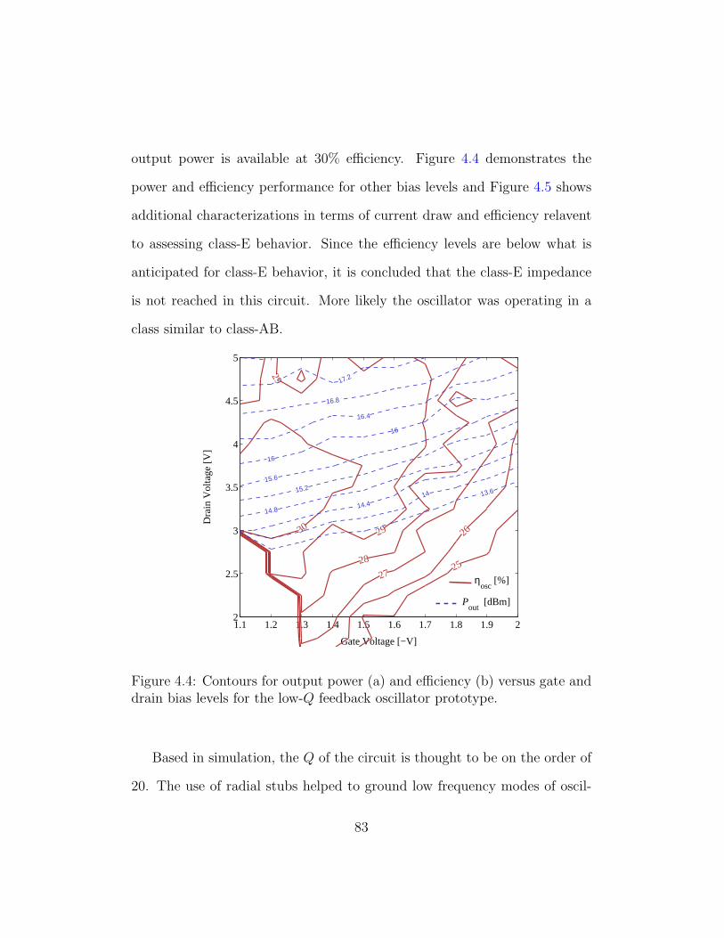
output power is available at 30% efficiency. Figure 4.4 demonstrates the
power and efficiency performance for other bias levels and Figure 4.5 shows
additional characterizations in terms of current draw and efficiency relavent
to assessing class-E behavior. Since the efficiency levels are below what is
anticipated for class-E behavior, it is concluded that the class-E impedance
is not reached in this circuit. More likely the oscillator was operating in a
class similar to class-AB.
1.1 1.2 1.3 1.4 1.5 1.6 1.7 1.8 1.9 22
2.5
3
3.5
4
4.5
5
Gate Voltage [−V]
Dra
in V
olta
ge [V
]
25
26
2728
2930
29 17.2
16.8
16.4
16
15.6
16
15.2
14.814.4
13.614
ηosc
[%]
Pout
[dBm]
Figure 4.4: Contours for output power (a) and efficiency (b) versus gate anddrain bias levels for the low-Q feedback oscillator prototype.
Based in simulation, the Q of the circuit is thought to be on the order of
20. The use of radial stubs helped to ground low frequency modes of oscil-
83
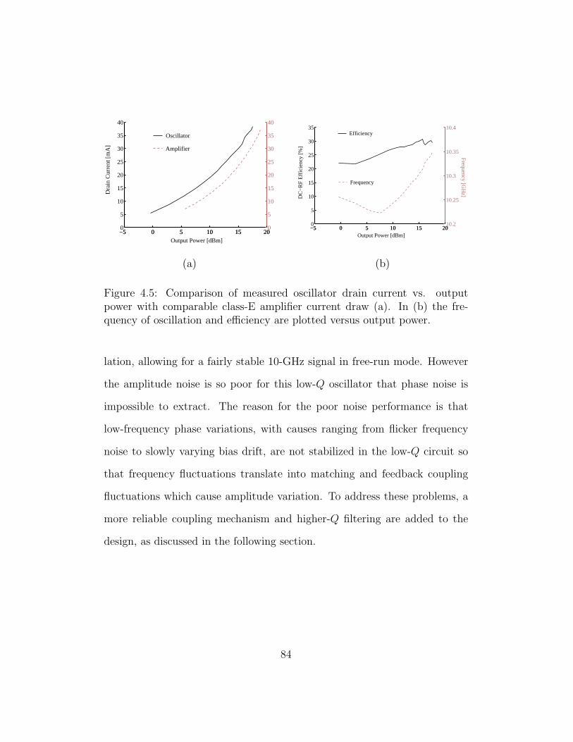
−5 0 5 10 15 200
5
10
15
20
25
30
35
40
Output Power [dBm]
Dra
in C
urre
nt [m
A]
Oscillator
−5 0 5 10 15 200
5
10
15
20
25
30
35
40
Amplifier
−5 0 5 10 15 200
5
10
15
20
25
30
35
Output Power [dBm]
DC
−R
F E
ffici
ency
[%]
Efficiency
−5 0 5 10 15 2010.2
10.25
10.3
10.35
10.4
Frequency [G
Hz]
Frequency
(a) (b)
Figure 4.5: Comparison of measured oscillator drain current vs. outputpower with comparable class-E amplier current draw (a). In (b) the fre-quency of oscillation and efficiency are plotted versus output power.
lation, allowing for a fairly stable 10-GHz signal in free-run mode. However
the amplitude noise is so poor for this low-Q oscillator that phase noise is
impossible to extract. The reason for the poor noise performance is that
low-frequency phase variations, with causes ranging from icker frequency
noise to slowly varying bias drift, are not stabilized in the low-Q circuit so
that frequency uctuations translate into matching and feedback coupling
uctuations which cause amplitude variation. To address these problems, a
more reliable coupling mechanism and higher-Q ltering are added to the
design, as discussed in the following section.
84

4.5 Improved class-E Oscillator Design
To gain more control on parameters such as feedback coupling ratio and os-
cillation frequency, the previous low-Q design is modied in ve important
ways: 1) A well characterized 4-port coupler is used for the feedback; 2) A
resonator with Q on the order of 150 is added to the circuit; 3) The oscilla-
tor is designed around an independent amplier design; 4) The oscillator is
modeled as two back-to-back ampliers; 5) Measurements of the nonlinear
phase through the transistor are used to design the closed-loop path length.
4.5.1 Asymmetric Branch-line Coupler
A coupler is desired which can provide low return loss and specic coupling
over the bandwidth of potential oscillating frequencies. The tee-junction
used in the previous section was seen to contribute to amplitude noise due to
its frequency sensitive coupling characteristics. In this section a branch-line
coupler is investigated as an alternative which requires an isolated port but
also provides a good handle on the feedback mechanism in the oscillator.
Since a specied amount of coupling is desired, a convenient design for
an asymmetric 4-port branch-line coupler is used. The coupler is designed
according to guidelines given in [48] by using the following equations:
Za = 50jS21jjS31j
and Zb = 50
sjS21j2
jS21j2 + jS31j2(4.7)
where Za is the characteristic impedance of the series sections of the
85

Figure 4.6: Photograph of the asymmetric branch-line coupler designed for-7.4 dB coupling (S31).
branchline coupler and Zb that of the shunt sections: S21 refers to scattering
to the through port and S31 to the coupled port referenced to the input port.
Based on the analysis of optimal feedback level performed earlier, a cou-
pling ratio of -7.1 dB was designed for. A photograph of the resulting coupler
is shown in Figure 4.6. For -7.1 dB coupling from port-1 to port-3 in Fig-
ure 4.6, 106Ω and 45.2Ω lines were required. Measurements on the coupler
86
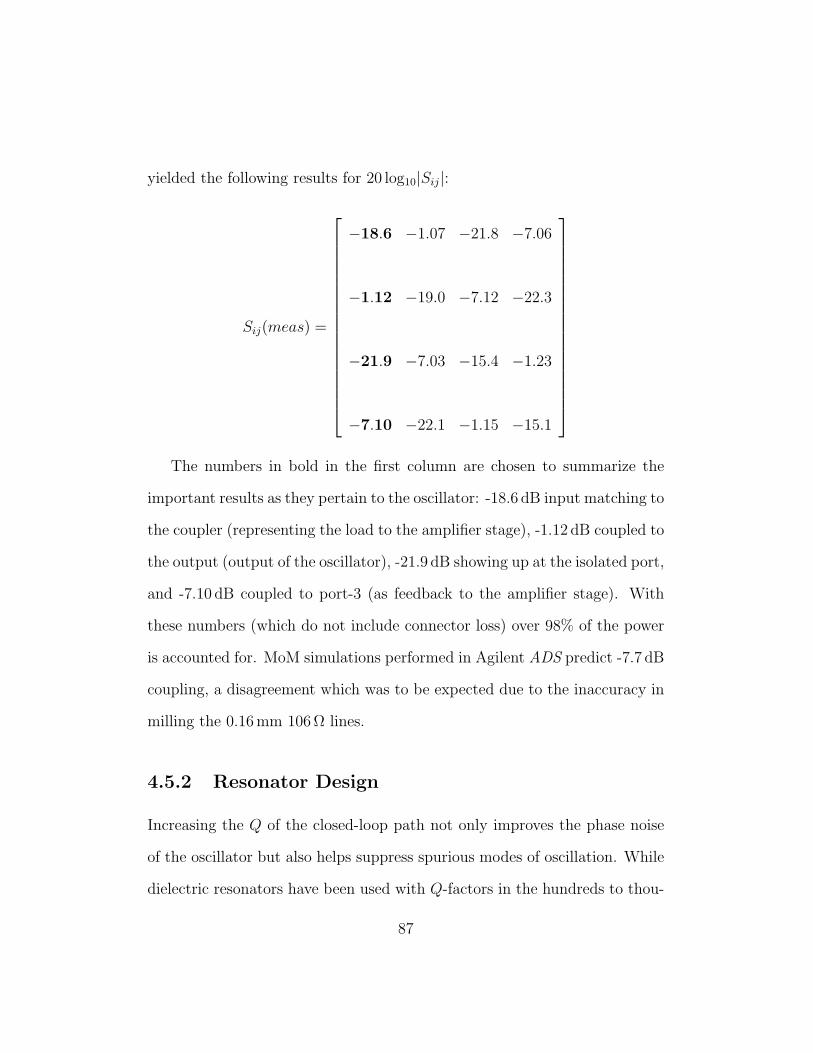
yielded the following results for 20 log10jSijj:
Sij(meas) =
2666666666666666664
−18:6 −1:07 −21:8 −7:06
−1:12 −19:0 −7:12 −22:3
−21:9 −7:03 −15:4 −1:23
−7:10 −22:1 −1:15 −15:1
3777777777777777775The numbers in bold in the rst column are chosen to summarize the
important results as they pertain to the oscillator: -18.6 dB input matching to
the coupler (representing the load to the amplier stage), -1.12 dB coupled to
the output (output of the oscillator), -21.9 dB showing up at the isolated port,
and -7.10 dB coupled to port-3 (as feedback to the amplier stage). With
these numbers (which do not include connector loss) over 98% of the power
is accounted for. MoM simulations performed in Agilent ADS predict -7.7 dB
coupling, a disagreement which was to be expected due to the inaccuracy in
milling the 0.16mm 106Ω lines.
4.5.2 Resonator Design
Increasing the Q of the closed-loop path not only improves the phase noise
of the oscillator but also helps suppress spurious modes of oscillation. While
dielectric resonators have been used with Q-factors in the hundreds to thou-
87
sands, a more convenient microstrip ring coupler is used here as implemented
by [49, 50, 51]. What is more, the coupling arms to the ring can be adjusted
(using an x-acto knife) to tune the resonance frequency and, in turn, the
closed-loop phase. Therefore the ring coupler is used as the primary post-
production tuning mechanism. The layout of the ring coupler is shown as it
was used in the oscillator in Figure 4.7.
Figure 4.7: Photograph of the two-port microstrip ring resonator with cou-pling arms.
Based on measured results, the loaded Q of the ring coupler was approx-
imately 100. It was also found that frequency and phase can be tuned from
10.1GHz down to 9.97GHz (f = −40MHz) with a thru-phase change of
= −38 by shortening the coupling arms 16 (from the center of the
ring). By comparison, a 50Ω line on this substrate changes by = −10:4
88

over the same frequency span. The thru loss, or S21, of the coupler was mea-
sured to be -0.5 dB before tuning. The loss increases as much as 1.2 dB as
the arms are shortened by 70. Not unimportantly, the coupled lines to the
ring also provides isolation from DC to 10GHz between its input and output
ports, both helping to block low frequency oscillations and serving to replace
a dc-blocking capacitor.
4.5.3 Two-stage Amplifier Analysis
The class-E amplier is placed in the environment of an oscillator by pre-
senting its output with the coupled input of an identical amplier operating
under the same conditions. By doing this, it is possible to draw several
conclusions about theoretical oscillator performance before building the os-
cillator itself. In fact every aspect of the oscillator is determined except for
the phase path (length of 50 Ω required for the oscillation condition) and
additional resonator.
The design layout of Figure 4.8 shows the feedback oscillator divided
into two parts: the active amplier stage with matching networks and the
passive 4-port coupler consisting of input (1), output (2), isolated (3), and
coupled(4) ports. The design procedure addresses the following questions
and unknowns:
1) Can the amplier, operating in the nonlinear class-E mode, be modeled
as a 50Ω Thevenin source to drive the coupler at b1.
2) Is the input impedance of the amplier sufficiently matched to 50Ω to
89

Figure 4.8: Schematic of the class-E oscillator with ports labeled for compar-ison to the two-stage circuit. Ports a1 and b1 relate to the input and outputports shown in Figure 4.9, while the output refers to Psigh. The unknownwill remain the phase lengths l.
properly load the coupler at a1.
3) If not well matched, how much power is then lost in the isolated port.
4) How much output power and what DCRF efficiency can we expect
from the oscillator.
5) Are there any spurious oscillations due to amplier S12 or other reasons.
The phase through the amplier and through the coupler will be measured
separately using a Network Analyzer. The remaining path length needed
for 2n total phase will be estimated using MoM simulations together with
additional Network Analyzer measurements.
90

Figure 4.9: Photograph of the two-stage amplier with identical class-E am-pliers and asymmetric branch-line coupler.
The two stages behave differently when the gain of the rst stage deviates
from 7.1 dB, i.e. the input power to the second stage is different from the
input power to the rst stage. Therefore we are interested in the instances
where the gain of both stages are near 7.1 dB for the same bias point on
each amplier. After locating a set of operating points (bias point and in-
put power) where the two gains are equal, the power levels at the various
ports must be compared. If they are roughly equal, then we can conrm the
assumption that the two-stage amplier is operating in an equivalent envi-
ronment to an oscillator. Table 4.3 shows ve cases where the gains of each
stage are equal.
To extend these results to a hypothetical oscillator, the oscillator output
power corresponds to Psig and the DCRF efficiency corresponds to (either)
91

Table 4.3: Summary of the two-stage test (refer to Figure 4.9)
bias G1 G2 Pout1 Pout2 Pin1 Pin2
dB dB dBm dBm dBm dBm
Vds = 3.8 VVgs = −1.2 V 7.06 7.01 18.4 18.3 11.3 11.3Vds = 3.9 V
Vgs = −1.3 V 7.08 7.04 18.4 18.3 11.3 11.3Vds = 4.3 V
Vgs = −1.4 V 7.11 7.14 18.9 18.9 11.8 11.8Vds = 4.1 V
Vgs = −1.5 V 7.02 7.12 18.3 18.3 11.2 11.3Vds = 3.9 V
Vgs = −1.6 V 7.07 7.25 17.4 17.6 10.3 10.3
bias PAE1 PAE2 Psig Piso Prefl
% % dBm dBPout1 dBPin1
Vds = 3.8 VVgs = −1.2 V 43.8 44.9 17.2 -13.1 -13.4Vds = 3.9 V
Vgs = −1.3 V 44.4 46.1 17.3 -13.7 -14.8Vds = 4.3 V
Vgs = −1.4 V 43.7 46.7 17.8 -14.2 -15.5Vds = 4.1 V
Vgs = −1.5 V 44.2 47.8 17.2 -14.8 -16.6Vds = 3.9 V
Vgs = −1.6 V 43.8 48.8 16.3 -15.7 -15.9
92

PAE. The best case scenario found in these measurements is a Psig =
17:8 dBm at roughly 45% efficiency. As mentioned before, higher PAE can
result by allowing higher gain. This is done by altering the coupler for less
coupling (S31 < −7:1 dB) which will also allow more output power Psig.
The result that more gain is needed is part of what this design test was
meant to reveal. It has also been shown that we can observe class-E behavior
in an oscillator environment. These results can then be used together with
a phase path study to nish the oscillator design.
4.5.4 Phase Measurements
The closed loop phase of the oscillator must be 2n to optimize the oscillation
condition. This is equivalent to setting the reactance of the output of the
transistor to the negative of the transistor reactance. The phase (reactance)
of the transistor, however, is a function of input power to the device and
bias level. Therefore a characterization of the thru phase is in order. The
phase through the same class-E test amplier is measured as a function of
gate bias, drain bias and input power (Figure 4.10). The result is used for
design of the excess transmission line path length and for post fabrication
ne tuning.
93

4 6 8 10 12 14−105
−100
−95
−90
−85
Input Power [dBm]
Am
p th
ru P
hase
[deg
rees
]
4 6 8 10 12 14−105
−100
−95
−90
−85Vds
= 3 VVds
= 2 V Vds
= 4.2 VVds
= 3.5 V
upper line: Vgs
= −1.7 V
middle line: V
gs = −1.5 V
lower line: Vgs
= −1.3 V
Figure 4.10: Measurements of nonlinear amplier phase response.
4.5.5 Mid-Q Oscillator
The stand alone class-E oscillator, asymmetric branch-line coupler and micro-
strip ring resonator are incorporated into a class-E oscillator design (Fig-
ure 4.11. To date, two iterations of the oscillator have not produced 10-GHz
oscillations. The immediate culprit is the path length of the feedback loop.
Since 90 at 10GHz in this substrate is x mm, and the overall path length
is y mm, the room for fabrication error turns out to be substantial. The
best solution appears to be to build several oscillators each with graded path
lengths (rather than adding a lossy tuning mechanism). As mentioned be-
fore, tuning the ring couplers coupling arms provides 20 or more of tuning,
therefore a limited number of iterations should nd the proper phase.
While 10-GHz oscillations proved elusive after two iterations, the fact
94

Figure 4.11: Photograph of the oscillator design with implementation ofthe stand alone class-E amplier, asymmetric branch line coupler, and ringresonator.
that the circuit did not oscillate anywhere is a promising result. This proves
that the Q of the circuit is high enough to block oscillations at all frequencies
except at its resonance frequency, and possibly harmonics of that frequency.
However since an open circuit at 20GHz is presented at the output of the
device, and since the device can support little gain at 30GHz, oscillations at
these frequencies are not anticipated.
As a sanity check, a coaxial probe was used to inject the circuit with power
near 10GHz. It was concluded that the biased device successfully amplied
this injected power. However, since no oscillations could be coaxed, the
conclusion was further substantiated that the feedback was destructive.
95

Chapter 5
DC–Radiated RF Waves:
A Self-Oscillating Annular Ring
5.1 Motivation
Free-space power combining of distributed oscillating elements presents a
high-efficiency solution to microwave dc-rf conversion. By distributing sources
in an array, transmission lines, combiners, and associated losses can be re-
duced or eliminated. Furthermore, the circuit size of the individual oscillat-
ing elements can be greatly reduced by incorporating the antenna element
directly as a resonator and feedback circuit. Early designs have combined
the radiating element as a load with a stand-alone oscillator and separate
feedback loop. More recent designs have used rectangular patches as a radia-
tor in the feedback path [54, 55, 56]. FETs were also directly integrated into

the radiating element using modied antenna geometries for direct match-
ing [57, 58]. Similarly a 100-MESFET grid oscillator capable of high output
power and gain was rst reported in [59].
DC RF
transistor
feedback loop
transmittingantenna
receiver
Figure 5.1: Diagram of a self-oscillating antenna with DC supply and ra-diation mechanism. The amount of RF available to the receiver system isdescribed by the ERP . The efficiency at which the DC is converted to thereceived RF is described by the isotropic conversion gain, Giso.
In this chapter, the advantages of using a compact single layer, high gain,
switched mode integrated oscillating antenna are investigated. The perfor-
mance of the unit cell is then assessed as an element for a high-efficiency
power combining array. A microstrip annular ring has been chosen to im-
prove the radiation characteristics and to reduce microstrip circuitry over
conventional designs. The entire circuit is enclosed inside the ring allow-
ing for straight-forward, compact array design. High-efficiency is afforded
by switched mode transistor operation, high antenna gain, and potential for
high array packing density.
The fundamental role of self-oscillating antennas is to convert as much
97

available DC energy to RF at a distant receiving aperture. Applications in-
clude short range free space power beaming as in [20] and long range systems
as in the Space Power System (SPS) [8] where sunlight is converted to DC
on a satellite, then converted to RF and beamed to a ground-based collector
site. Another application is Doppler sensing as in [60]. As will be shown, the
linear frequency tuning of the oscillator allows for local mixing of a re ected
signal. Interestingly, neither application requires low phase noise. In fact, a
tunable oscillator must have higher phase noise for a greater tuning range.
The ring presented here is a low-Q resonator for the oscillator and no attempt
is made in this work to improve the phase noise.
5.2 The Active Ring
5.2.1 Analysis Tools
To aid in the design of the active ring antenna, analytical equations and
method of moments (MoM) solvers (for antenna design), linear and non-linear
circuit solvers (ADS and Momentum), and measurement-based models (from
switched-mode ampliers) were used. A modal analysis of the ring structure
was performed by solving the transcendental equation
J′
n(kb)Y′
n(ka)− J′
n(ka)Y′
n(kb) = 0 (5.1)
where the mth zero of the nth order Bessel function corresponds to the
resonant frequency of the TMnm mode and b and a are the outer and inner
98

(a) (b)
Figure 5.2: Photograph of the 10-GHz active ring (a) and simulated depictionof the total current density distribution for the TM12 operating mode (b).
radii of the annulus. Equation 5.1 and the equations for the E and Hplane
radiation given by
E = jn 2Eo
knm
e−jkor
rkoh
J ′
n(koa sin)− J ′n(knma)
J ′n(knmb)
J ′n(kob sin)
cosn (5.2)
E = −njn 2Eo
knm
e−jkor
rkoh
Jn(koa sin)
koa sin− J ′
n(knma)
J ′n(knmb)
Jn(kob sin)
kob sin
sinn cos
(5.3)
are derived from a cavity model of the annular ring [61]. More accurate solu-
tions for input impedance, radiation patterns, and two-port behavior of the
ring were performed using Zeland IE3D and Ansoft Ensemble MoM solvers.
The linear circuit solver and nonlinear harmonic balance solver from Agilent
ADS were also used to simulate the integrated antenna and transistor. In
99

addition to simulation, the ring design is also heavily based on measurements
of passive rings and class-E ampliers, as done in Chapter 4.
5.2.2 Figures of Merit
Figures of merit for the active ring fall into the following three categories:
Oscillator performance:
Pout: the output power in the fundamental frequency leaving the device.
ηosc = Pout/Pdc: DCRF efficiency where Pdc = VdsIds.
Antenna performance:
Plat: lateral radiatied power in the Eplane normalized to broadside.
Gant: the antenna gain.
Integrated performance
ERP = (4πR)2·Prcv
2Grcv= PoutGant: effective isotropic radiated power.
Giso = ERP/Pdc = Gant ηosc: the isotropic conversion gain.
The effective radiated power and DC power are the directly measurable
quantities. Their quotient, Giso, is a measure of how efficiently DC power
has been converted into a directed, linearly polarized beam. The isotropic
conversion gain is the most important parameter for an active antenna whose
goal is efficient power transfer.
100

5.3 Antenna Design
The microstrip annular ring, operating in the TM12 mode is chosen primarily
for its convenience as a two port coupling mechanism and the ease with which
its radiation pattern can be controlled. Analysis of the antenna as a two-port
is addressed in the following section while the design and characterization of
a passive one-port annular ring are the topics of this section.
5.3.1 Lateral Radiation
In order to operate in a densely packed array, the single element is designed
for minimal lateral radiation. Lateral radiation is dened as the radiated
power at the angels = −90, +90 (also radiation in the azimuth plane).
In fact it has been shown that lateral radiation is a greater contributer to
mutual coupling between nearest neighbors than surface wave excitation [62].
At the same time, the two are related by the patch geometry and suppres-
sion of one leads to suppression of the other. In most patch antennas, lateral
radiation and surface wave excitation are not easily suppressed without elab-
orate designs [63]. However, operating the annular ring in the TM12 mode
allows for optimization of the b/a ratio (outer/inner ratio) for minimal lateral
radiation, Plat. Furthermore, reducing Plat leads to an increase in antenna
gain and therefore, improved Giso.
The lateral co-polarized radiation in the Hplane is theoretically null,
and is therefore typically very low (30 to 40 dB down from the broadside
101

Figure 5.3: Calculated Eplane radiation patterns from Equation 5.2 as afunction of b/a ratio.
radiation) in practice. The lateral co-polarized Eplane radiation, however,
is directly dependent on the ring geometry, as is evident from Equation 5.2.
This can also be understood from Figure 5.2 (b) which shows that the two
regions of current maxima form an effective two-element array. If the array
is spaced properly, then lateral nulls can be achieved in the Eplane as well
with greatly reduced radiation in all other lateral directions including cross-
polarized radiation (which is a concern for the TM12 mode).
The three cases shown in Figure 5.3 illustrate how the Eplane radiation
pattern changes with ring geometry (a change in b/a ratio requires rescaling
to maintain resonance at the same frequency). The level of Plat in the E
plane is computed as a function of b/a using Equation 5.2 and the chosen
substrate parameters and plotted in Figure 5.4. The curves of Figure 5.4 are
specic to the substrate parameters chosen, in this case the Rogers TMM10i
102
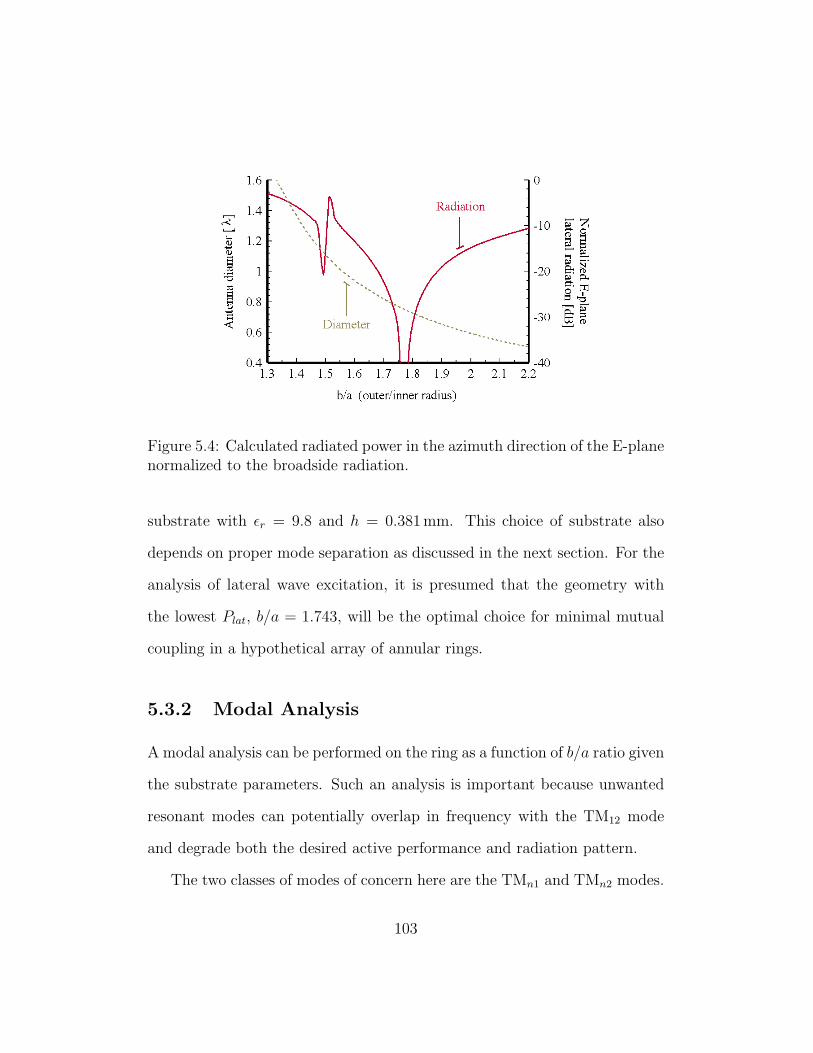
Figure 5.4: Calculated radiated power in the azimuth direction of the E-planenormalized to the broadside radiation.
substrate with r = 9:8 and h = 0:381mm. This choice of substrate also
depends on proper mode separation as discussed in the next section. For the
analysis of lateral wave excitation, it is presumed that the geometry with
the lowest Plat, b/a = 1:743, will be the optimal choice for minimal mutual
coupling in a hypothetical array of annular rings.
5.3.2 Modal Analysis
A modal analysis can be performed on the ring as a function of b/a ratio given
the substrate parameters. Such an analysis is important because unwanted
resonant modes can potentially overlap in frequency with the TM12 mode
and degrade both the desired active performance and radiation pattern.
The two classes of modes of concern here are the TMn1 and TMn2 modes.
103
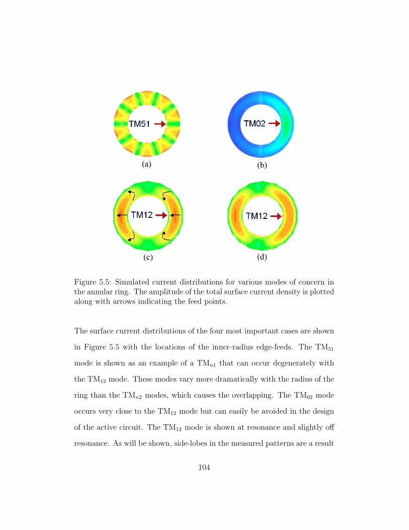
Figure 5.5: Simulated current distributions for various modes of concern inthe annular ring. The amplitude of the total surface current density is plottedalong with arrows indicating the feed points.
The surface current distributions of the four most important cases are shown
in Figure 5.5 with the locations of the inner-radius edge-feeds. The TM51
mode is shown as an example of a TMn1 that can occur degenerately with
the TM12 mode. These modes vary more dramatically with the radius of the
ring than the TMn2 modes, which causes the overlapping. The TM02 mode
occurs very close to the TM12 mode but can easily be avoided in the design
of the active circuit. The TM12 mode is shown at resonance and slightly off
resonance. As will be shown, side-lobes in the measured patterns are a result
104
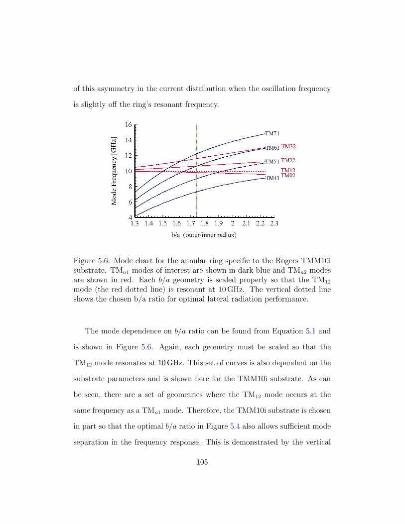
of this asymmetry in the current distribution when the oscillation frequency
is slightly off the ring's resonant frequency.
Figure 5.6: Mode chart for the annular ring specic to the Rogers TMM10isubstrate. TMn1 modes of interest are shown in dark blue and TMn2 modesare shown in red. Each b/a geometry is scaled properly so that the TM12
mode (the red dotted line) is resonant at 10GHz. The vertical dotted lineshows the chosen b/a ratio for optimal lateral radiation performance.
The mode dependence on b/a ratio can be found from Equation 5.1 and
is shown in Figure 5.6. Again, each geometry must be scaled so that the
TM12 mode resonates at 10GHz. This set of curves is also dependent on the
substrate parameters and is shown here for the TMM10i substrate. As can
be seen, there are a set of geometries where the TM12 mode occurs at the
same frequency as a TMn1 mode. Therefore, the TMM10i substrate is chosen
in part so that the optimal b/a ratio in Figure 5.4 also allows sufficient mode
separation in the frequency response. This is demonstrated by the vertical
105

dotted line in Figure 5.6 which represents the optimal b/a for minimal lateral
radiation.
A third consideration for substrate choice is the electrical size of the
antenna. The thin substrate allows for additional suppression of substrate
modes while the high dielectric constant and the chosen b/a ratio lead to a
ring whose diameter is approximately 0.75o.
5.3.3 Passive Measurements
The design of the ring is based on minimized lateral radiation, mode separa-
tion, and convenient circuit and array size. The design is shown in Figure 5.2
and is summarized in Table 5.1.
Table 5.1: Summary of design parameters for the passive ring. The substrateparameters are relative dielectric, r, substrate thickness, h, and metalizationlayer thickness, t. The physical parameters of the ring are dened by b anda, the outer and inner radii.
r h t b a b/a
9.8 25 mil 9 10.79mm 6.19mm 1.743
The measured frequency response of the passive ring compares well with
the predicted results of Figure 5.6 and with MoM simulations as shown in
Figure 5.7. Adequate separation of the TM51 and TM61 modes is achieved
and TM12 resonance occurs at 9.95GHz.
Radiation patterns were taken in a 4-m anechoic chamber and again com-
pared with MoM simulations. The results, displayed in Figure 5.8, show the
106
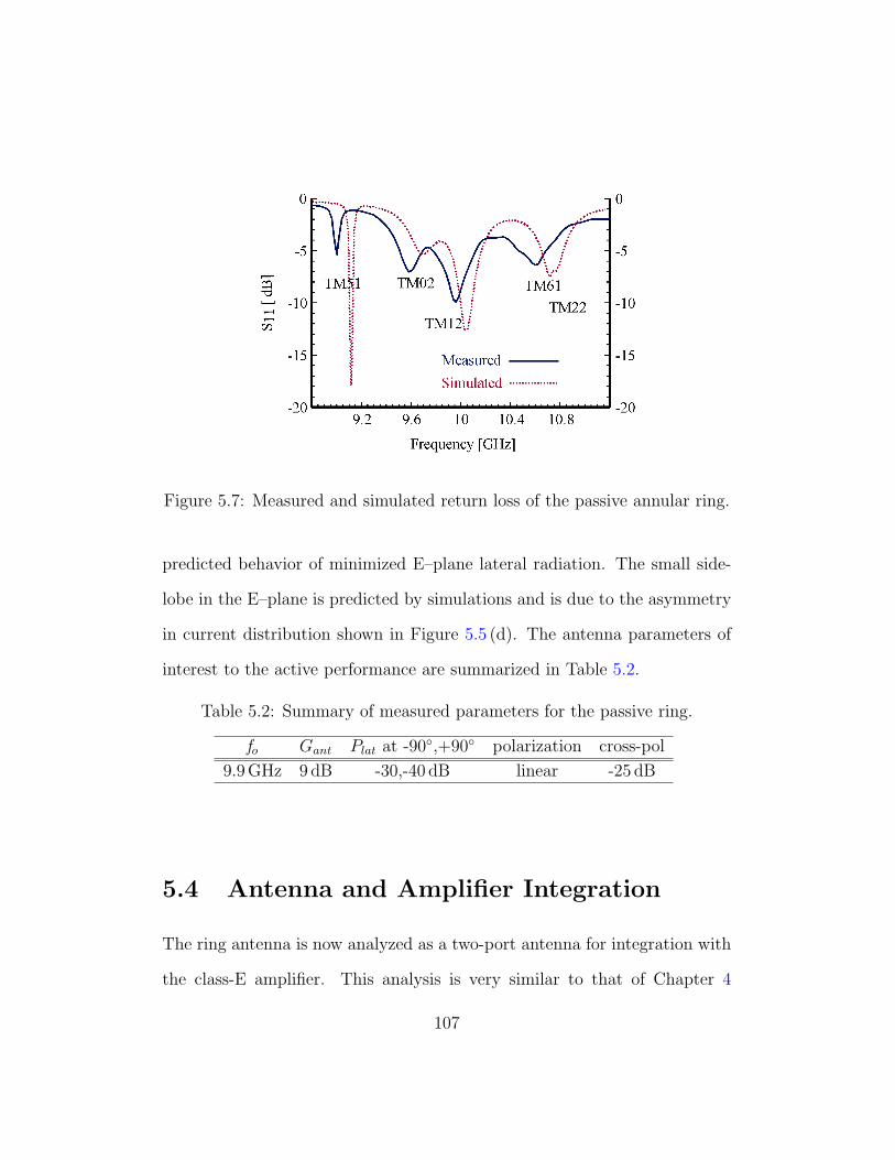
Figure 5.7: Measured and simulated return loss of the passive annular ring.
predicted behavior of minimized Eplane lateral radiation. The small side-
lobe in the Eplane is predicted by simulations and is due to the asymmetry
in current distribution shown in Figure 5.5 (d). The antenna parameters of
interest to the active performance are summarized in Table 5.2.
Table 5.2: Summary of measured parameters for the passive ring.
fo Gant Plat at -90,+90 polarization cross-pol
9.9GHz 9 dB -30,-40 dB linear -25 dB
5.4 Antenna and Amplifier Integration
The ring antenna is now analyzed as a two-port antenna for integration with
the class-E amplier. This analysis is very similar to that of Chapter 4
107

(a) (b)
Figure 5.8: Measured and simulated radiation patterns in the Eplane (a)and Hplane (b) for the passive annular ring.
with the exception that the ring antenna is used in place of the asymmetric
branch-line coupler.
5.4.1 Class-E Oscillation
As in Chapter 4, a stand-alone class-E amplier with 50-Ω input and output
impedances is swept over a large range of bias levels and input powers. The
measured Pout, Gamp, return loss (RL), and PAE over the swept values pro-
vided signicant insight into the anticipated class-E oscillator performance.
The two plots of Figure 5.9 show how Pout and ηosc vary with bias and feed-
back level. While Chapter 4 deals with varying feedback levels for a small
108

range of bias points, Figure 5.9 shows how the efficiency varies beyond the
standard class-E bias point. The design and fabrication steps for the active
ring are much more difficult than those for the planar oscillator, and there-
fore the actual feedback level is harder to pinpoint. Therefore, these two
additional graphs are an important tool not only for the design, but also
for diagnosing sub-optimal performance. Essentially, Figure 5.9 shows that
an optimal feedback region between -6 and -9 dB can be used provided the
correct bias.
5.4.2 Port Matching
The class-E oscillator in Chapter 4 uses a four-port coupler with 50-Ω input,
coupled, isolated, and output ports. Here, the ring can be considered as a
three-port coupler with unmatched input, coupled, and output ports where
the output port is free-space radiation. The two-port antenna, shown in
Figure 5.10, must provide the proper coupling ratio from port-1 to port-2
while presenting the proper load at port-1 for class-E operation. The design
process is necessarily iterative and only the nal result will be shown here.
Figure 5.10 (b) and Figure 5.11 (b) will be used to show how the microstrip
circuitry connecting the transistor to the antenna are used together with the
antenna to force the desired coupling and class-E match.
As described in Figure 5.10 (b), the port-1 impedance looking into the
antenna is known, approximately, from measurements and simulation, but
also depends on the port-2 load. The region is in effect a region on the Smith
109

(a)
(b)
Figure 5.9: Bias regions for various feedback levels where predicted 50%efficiency and within 3 dB of the maximum power (indicated) occur together(a). Maximum efficiency and associated power for any bias point as a functionof feedback (b).
110

(a) (b)
Figure 5.10: The impedance looking into port-1 of the antenna (a) is known tobe in the red solid region on the smith chart in (b). The actual location of theimpedance depends on the subsequent loading of port-2. The impedance ofport-1 is transformed by the tuning stubs on the output side of the transistorto the class-E impedances at the rst and second harmonics.
chart that moves as a function of the port-2 loading and which can be trans-
formed with the transistor output stubs to the class-E output impedance.
The Smith chart of Figure 5.11 (b) represents the possible impedance
transformations of the transistor input (gate). This is simulated by nding
the two-port S-parameters of the ring with MoM solvers and simulating a
source and load-pull over the Smith chart on the two ports. Figure 5.11 (b)
primarily demonstrates the resulting coupling factor as a function of the
port-2 load. It can be seen that the desired coupling factor (around -7 dB
in this case) can be achieved for a set of transformations forming a ring on
111
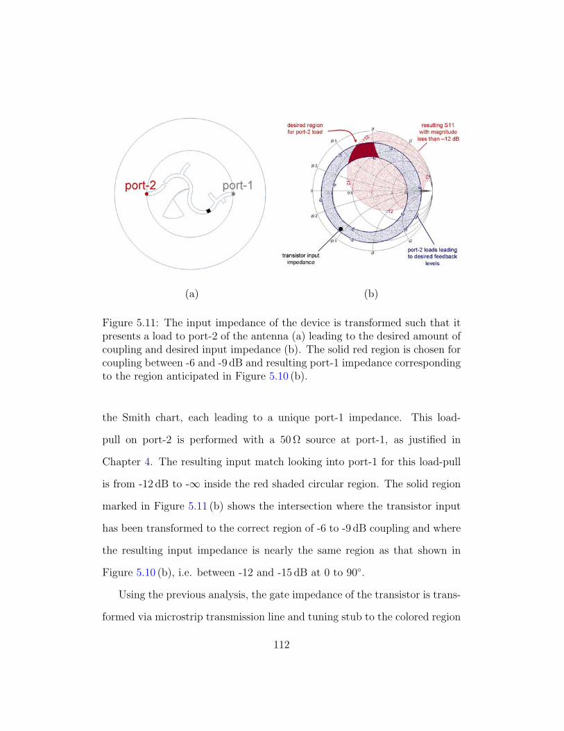
(a) (b)
Figure 5.11: The input impedance of the device is transformed such that itpresents a load to port-2 of the antenna (a) leading to the desired amount ofcoupling and desired input impedance (b). The solid red region is chosen forcoupling between -6 and -9 dB and resulting port-1 impedance correspondingto the region anticipated in Figure 5.10 (b).
the Smith chart, each leading to a unique port-1 impedance. This load-
pull on port-2 is performed with a 50Ω source at port-1, as justied in
Chapter 4. The resulting input match looking into port-1 for this load-pull
is from -12 dB to -1 inside the red shaded circular region. The solid region
marked in Figure 5.11 (b) shows the intersection where the transistor input
has been transformed to the correct region of -6 to -9 dB coupling and where
the resulting input impedance is nearly the same region as that shown in
Figure 5.10 (b), i.e. between -12 and -15 dB at 0 to 90.
Using the previous analysis, the gate impedance of the transistor is trans-
formed via microstrip transmission line and tuning stub to the colored region
112

on the Smith chart in Figure 5.11 (b). Subsequently, the resulting impedance
looking into the antenna at port-1 can be transformed in the same way to
present the class-E match at the output of the transistor. The second har-
monic impedance seen by the transistor output should be an open circuit
and is accomplished using an open stub (the stub nearest the device). This
section has addressed the matching necessary to connect the antenna with
the active device. The following section completes the design considerations
and summarizes the three-port active behavior.
5.4.3 Loop Analysis
A loop analysis is performed in order to test the integrated antenna and
amplier as a potential oscillator. The loop gain is set by the amount of
feedback designed into the passive structure. The loop phase must now be
designed for 2n radians in order to meet the oscillation condition. This
is done with the circuit simulator in ADS by rst breaking the loop after
the device, as shown in Figure 5.12. The simulation is then performed on
the microstrip lines and S-parameter blocks representing the two-port device
and two-port antenna. The microstrip lines are designed to simultaneously
provide the matching required by the previous section and the 2n round-
trip phase. A solution for the microstrip layout favorable for the amount of
room inside the ring is subsequently realized using meander lines and open
stubs.
The loop simulation can also provide some insight into the loop behavior
113

(a) (b)
Figure 5.12: The loop gain and phase described by the path in (a) is analyzedby breaking the circuit at the output of the device and driving it with a testvoltage (using ADS). The result of the loop S21 (b)can be compared withFigure 5.7 to see how the TM12 mode is excited while other modes can notsupport oscillations. The ow of power in (a) is from left to right in themicrostrip lines, then right to left around the upper and lower arcs of thering.
as a function of frequency, as shown in Figure 5.12 (b). It should be noted
rst, however, that the gain and phase through the transistor are approximate
because the given S21 was originally measured under small-signal conditions
for one particular bias. Still, it can be seen how adjacent modes (compare to
Figure 5.7) are ltered and kept from oscillating, while there is positive loop
gain and proper phase within the TM12 mode.
114

5.5 Measurements
The ring is made using a milling machine and the transistor mounted with
conductive epoxy and connected using a pair of wire bonds each on the gate
and drain pads. As can be seen in Figure 5.2, a radial stub with via is used to
bring in the gate bias. An 8.2 pF high-frequency capacitor is used as a DC-
block from the drain bias which is supplied by a second via at the location
of a current maximum on the ring. This location is chosen as a secondary
measure to lter out other ring modes while leaving the TM12 mode relatively
unperturbed. Finally, the ring is mounted on a circular ground-plane with
30 cm diameter.
Measurements were taken in a computer controlled anechoic chamber
with 4m range. The DC-bias, RF-spectrum analysis, and antenna position
were controlled and monitored using Matlab. In this way the quantities fosc,
Prcv, and Ids were recorded as a function of Vgs and Vds or as a function of
, to measure the oscillation performance or antenna patterns, respectively.
5.5.1 Oscillator Performance
The bias voltages, Vgs and Vds, are the only inputs to the self-oscillating ac-
tive ring. The oscillation frequency as a function of Vgs and Vds is shown in
Figure 5.13. Each voltage is incremented in steps of 0.1V, and the measure-
ment represents 648 data points. The ring oscillates in the TM12 mode for all
bias points except for the region of very low Vgs where the gate was pinched
115
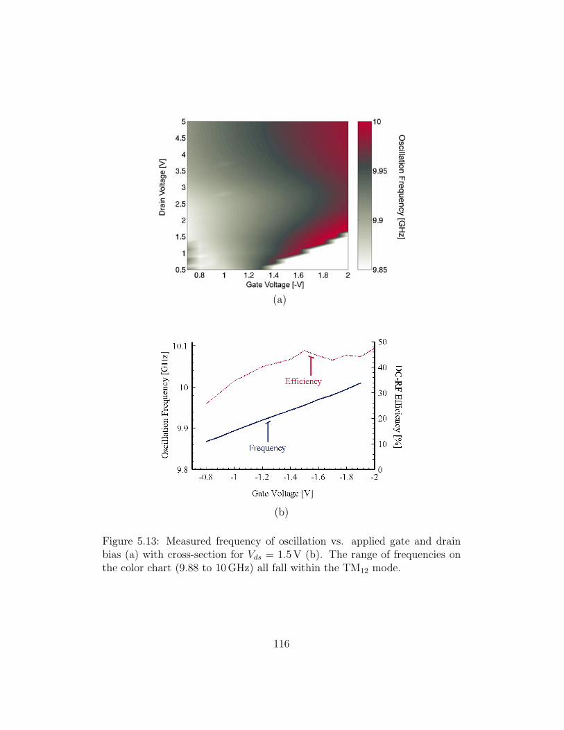
(a)
(b)
Figure 5.13: Measured frequency of oscillation vs. applied gate and drainbias (a) with cross-section for Vds = 1:5V (b). The range of frequencies onthe color chart (9.88 to 10GHz) all fall within the TM12 mode.
116

off and no current drawn. The range of oscillation frequencies spanned from
9.86 to 10.0GHz, a tuning range of 1.4% which ts safely in the bandwidth
of the TM12 mode (c.f. Figure 5.7).
The resulting Pout and ηosc are backed out from the measured Prcv and
Gant as discussed previously. The color plot of Figure 5.14 shows the optimal
region for efficiency over the same bias with additional contours for Pout.
The output power increases with drain voltage as expected. However, as will
be discussed, the high-efficiency region (dark-red region) coincides with the
lower power levels.
The plots of Figure 5.13 and Figure 5.14 re ect the amount of coupling
and quality of impedance matching, or how well the ring works as an oscil-
lator. They do not represent, however, any of the radiative properties of the
integrated antenna.
5.5.2 Antenna Performance
The active antenna patterns are investigated in order to characterize the
lateral radiation, analyze polarization, and compare the patterns to those
of the passive ring. The Eplane and Hplane cuts shown in Figure 5.15
are taken for the active ring oscillating at 9.9GHz along with corresponding
patterns for the passive ring, driven at the same frequency. Lateral radiation
in the Eplane is contained to -34 dB on one side of the antenna, but only
to -18 dB on the other. The most likely reason for this is that the via in the
patch used to bring in the drain bias not only radiates, but also perturbs
117

(a)
(b)
Figure 5.14: Color plot of the measured DC-RF efficiency with contoursfor the associated output power (a). A cross-section of ηosc and Pout forVgs = −1:3V is shown in (b).
118

(a) (b)
Figure 5.15: Measured Eplane (a) and Hplane (b) radiation patterns at9.95GHz compared to the passive patterns taken at the same frequency.
the currents more than was intended. Nevertheless, the agreement between
active and passive patterns is very close. This important result permits
the assumption that Gant(active) = Gant(passive), and consequently that
Pout = ERP/Gant(passive). Back-scattering is also increased for the active
ring due to bias, however still kept under -18 dB.
Three-dimensional patterns are taken by allowing the active ring to ro-
tate in both the and directions of a spherical coordinate system given by
(, , r). The receiving horn is also turned simultaneously in so that a com-
plete co or cross-polarized pattern can be taken over a hemisphere. Mercator-
type projections of the normalized 3D radiation patterns with color-scale in
119

(a) (b)
Figure 5.16: Measured co-polarized (a) and cross-polarized (b) radiationpatterns taken over a hemisphere of radiation shown in a Mercator-typeprojection.
(a) (b)
Figure 5.17: Measured co-polarized (a) and cross-polarized (b) radiationpatterns taken over a hemisphere of radiation shown in a three-dimensionalorthographic projection.
120

dB are shown for both polarizations in Figure 5.16. For comparison purposes,
an orthographic projection in the (, , r) coordinates is given in Figure 5.17
where color and r both represent the dB-normalized radiation. Both styles
of display show how the lateral radiation is well contained at -20 dB or lower
except for cross-polarized radiation in the Hplane. Furthermore, it can be
seen that while the main beam is linearly polarized, a signicant amount of
energy is lost to cross-polarized radiation off boresite. The antenna parame-
ters are summarized in the following section.
5.5.3 DC–Radiated RF Performance
The combined performance of the class-E oscillator and antenna is sum-
marized in Table 5.3. The table lists three bias points: one for the point
of maximum output power (or ERP ), another for maximum efficiency (or
Giso), and a third point compromising between the two. A fourth instance
is given for what is believed to be attainable for this design. Among the
numerous references on active antennas mentioned previously, the following
listed in Table 5.4 standout as a basis of comparison.
The active ring combines a high gain antenna (8.1 dB) with high DCRF
conversion (-3.1 dB) to achieve 5 dB isotropic conversion gain in a compact
element. Using the ring in the TM12 mode sacrices increased physical area
for antenna gain; however, the larger antenna size is made up for by the
compact nature of the microstrip circuitry. Therefore, this active antenna
design has the highest recorded isotropic conversion gain at 10GHz or above.
121

Table 5.3: Active ring performance for a high-power bias point, high-efficiency point, compromise between the two, and theoretically attainableperformance.
bias fosc Pout ηosc Gant Plat ERP Giso DC[V] [GHz] [dBm] [%] [dB] [dB] [dBm] [dB] [mW]
Vds = 3.5Vgs = −1.6 9.96 15 22 8 -17,-35 23 2.0 145Vds = 1.8Vgs = −1.4 9.95 11 45 8 -17,-35 19 4.5 28Vds = 2.0Vgs = −1.1 9.96 13 35 8 -17,-35 21 3.4 57
attainable:Vds = 4.3Vgs = −1.4 10.0 17.8 45 9 -30,-40 26.8 5.5 134
Table 5.4: Comparison of previous work in the eld for oscillator and ampli-er elements and arrays. The parameter class refers to the class of operationin the amplication stage. References marked ∗ are ampliers. The lasttwo rows refer to the theoretical 24 element array mentioned below based onthe class-E annular ring single element measurements(y) and theoreticallyattainable results(z) as given in Table 5.3.
fosc Pout ηosc Gant Plat ERP Giso
class [GHz] [dBm] [%] [dB] [dB] [dBm] [dB]
Martinez [55] C 10 NA 45 NA -10 26.1 NAHo [58] A 7.7 13.3 18 7.5 -13 20.8 0.1Birkland [64] A 6 NA NA NA -26 44.5 9.9Popovic [59] NA 5 27.2 20 16 NA 43.2 9Radisic∗ [65] F 2.6 24.4 63 5.8 -10 30.2 3.8Pajic∗ [42] E 10 32.3 52 19.8 -26 52.1 16.8
Array† E 10 24.8 45 20.5 < -20 41.8 17Array‡ E 10 31.6 45 20.5 < -30 52.1 17
122

Figure 5.18: ERP and Giso vs. Vds.
Figure 5.18 demonstrates the behavior of ERP and Giso over drain bias.
As mentioned previously, if designed properly these two parameters should
reach the same peak at roughly the same drain bias. The fact that they
do not indicates that the either the coupling factor or the class-E match
was substantially off. In Figure 5.19, the amplier measurements are used
to diagnose the problem by attempting to match the measured response of
the ring with various coupling scenarios. It was found that the ring mea-
surements agree well with a -3 dB coupling factor over a large bias region
in terms of output power, efficiency, and drain current. While this analysis
assumes that the class-E match for the ring was relatively close, the result
that the oscillator was over-coupled is plausible. It is in fact likely that the
microstrip lines and ring coupled more than anticipated. A -3 dB coupling
ratio would lead to deep compression levels at higher drain biases, accounting
123
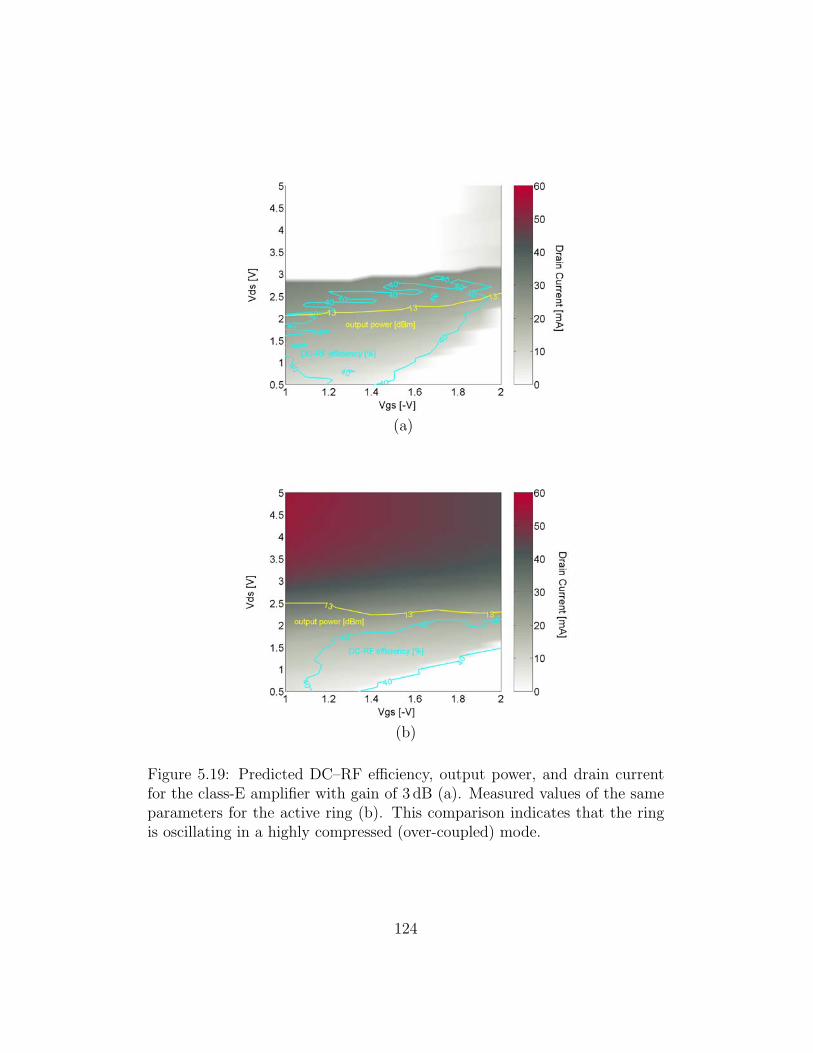
(a)
(b)
Figure 5.19: Predicted DCRF efficiency, output power, and drain currentfor the class-E amplier with gain of 3 dB (a). Measured values of the sameparameters for the active ring (b). This comparison indicates that the ringis oscillating in a highly compressed (over-coupled) mode.
124

for the lower efficiency at those levels. The coupling problem is addressed in
Chapter 6 (future and related work).
5.5.4 A Proposed Active Ring Array
Figure 5.20: Depiction of a proposed phase-locked array of ring oscillatorsfor a focused beam application.
The results shown above are a culmination of several fabrication attempts
at the same design. While fabrication tolerances can be a signicant source
of error, MoM simulations should also be performed on both the ring and
microstrip structures together to test for unintended coupling mechanisms.
It has been shown, however, that the ring can be used as a high-gain antenna
125

and two-port coupler appropriate for a high efficiency, self oscillating antenna.
Furthermore, the active appears to be a good candidate for an array based
on its reduced lateral radiation.
A proposed 24-element array, depicted in Figure 5.20, would require
proper phasing between the elements in order to focus the radiated energy
to a broadside beam. The reason for limiting the lateral radiation in the
single element was not only to increase the antenna gain, but also to allow
for controlled inter-element coupling. Inter-element coupling will allow the
individual rings to injection lock with a given phase delay. Surface-wave or
lateral-wave coupling does not allow precise control of the relative phase dif-
ferences. The addition of microstrip lines between the elements could provide
good control. However, the coupling carried by the microstrip lines must be
greater than the lateral wave coupling. Therefore, the lower the lateral wave
excitation, the better. The feasibility and application of such an array is
discussed further in Chapter 6.
126

Chapter 6
Related and Future Work
6.1 Microwave Rectification
On the topic of optimal RFDC conversion efficiency using harmonic ter-
minations, it was shown in Chapter 2 how the reverse breakdown voltage
is an impediment for certain rectication modes while the series resistance
is a greater factor in other modes. Therefore, the rst major challenge for
high efficiency microwave rectiers lies in selecting a diode with optimal pa-
rameters for the chosen class of operation. While semiconductor limitations
are always a convenient culprit for degraded efficiency performance, proper
semiconductor diode choice based on the Chapter 2 conclusions (Table 2.1)
can make a signicant difference in rectier performance.
A second challenge is fabrication related: Switched-mode rectiers are
only as efficient as the number of harmonic terminations that can be made

in the circuit [17]. However as a higher number of harmonic terminations
are required, the more difficult the fabrication and sensitive the impedance
value. Furthermore, physical space for transmission line terminations be-
comes crowded as the physical length of a quarter-wave section for a given
harmonic nears the cross-sectional size of the transmission line. In this case,
lumped-element terminations may become necessary.
6.2 Low-Power Rectenna Arrays
Unlike the high-efficiency rectiers discussed in Chapter 2, Chapter 3 dealt
with low-power RF-DC conversion of free-space waves with limited conver-
sion efficiency. While choice of the diode is an area of future concern, the
choice of the antenna element will make the most dramatic difference effi-
ciency numbers. While the spiral has many advantages for the application
of ambient energy recycling in planar form, it may be possible to optimize
a non-frequency independent geometry for a chosen diode over a certain fre-
quency band. As was stated in Chapter 2 the antenna can be optimized
separately once the diode has been characterized over the frequencies and
power of interest.
In addition to the antenna element, a study should be done to optimize
the effective aperture of a unit-cell relative to the range of wavelengths con-
sidered. This is tantamount to optimizing the number of diodes per center-
wavelength. For instance, if the surface of the rectenna array is divided into
128

too many rectifying elements, the response at lower band of interest will suf-
fer from aperture efficiency while the upper band will suffer from too little
input power per diode. If the antenna size is increased so that the number of
elements per surface area is small, then the aperture efficiency at the higher
frequencies will suffer, again resulting in too little input power. The optimal
solution is likely an array of graduated-sized antennas which make best use
of aperture efficiency and received power per diode.
6.3 Microwave Oscillators
The class-E oscillator presented in Chapter 4 was carried out with limited suc-
cess. Oscillations in class-E mode were never reached, which can be proved by
comparison with the predicted results. Instead a suboptimal class-E mode was
attained where the output power suffers slightly but the efficiency reached
was 30% rather than the anticipated 50%. On the other hand, a signicant
amount of progress was made towards optimizing a 10-GHz oscillator for
efficiency using the class-E mode. It was shown how proven high-efficiency
performance in the class-E amplier can be transferred to oscillator perfor-
mance by correct choice of the bias level in conjunction with the correct
feedback level. In addition, it was shown how the nonlinear phase response
of the transistor can be taken into account.
The major problem with the topology chosen here was the sensitivity
to path length in the feedback loop. Therefore, it is proposed that a dif-
129
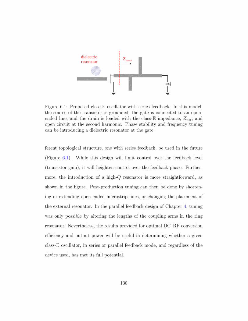
dielectricresonator
50W
Zclass-E
Figure 6.1: Proposed class-E oscillator with series feedback. In this model,the source of the transistor is grounded, the gate is connected to an open-ended line, and the drain is loaded with the class-E impedance, Znet, andopen circuit at the second harmonic. Phase stability and frequency tuningcan be introducing a dielectric resonator at the gate.
ferent topological structure, one with series feedback, be used in the future
(Figure 6.1). While this design will limit control over the feedback level
(transistor gain), it will heighten control over the feedback phase. Further-
more, the introduction of a high-Q resonator is more straightforward, as
shown in the gure. Post-production tuning can then be done by shorten-
ing or extending open ended microstrip lines, or changing the placement of
the external resonator. In the parallel feedback design of Chapter 4, tuning
was only possible by altering the lengths of the coupling arms in the ring
resonator. Nevertheless, the results provided for optimal DCRF conversion
efficiency and output power will be useful in determining whether a given
class-E oscillator, in series or parallel feedback mode, and regardless of the
device used, has met its full potential.
130

6.4 Oscillating Antenna Arrays
In Chapter 5, an integrated class-E oscillating annular ring was demonstrated
with 4.5 dB isotropic conversion gain. However the true advantages of using
using a high-efficiency, self-oscillating antenna manifest when the elements
are used in an array. The reason for this stems from the fact that the isotropic
conversion gain can be broken up into the product of DCRF efficiency and
antenna gain. In an array it is possible to increase the overall antenna gain
dramatically with no effect on the DCRF conversion rate. This is not true of
power combining amplier arrays using spatial or corporate feeds [69, 70]. In
those cases, losses increase with number of elements. Conversely, oscillating
arrays have no RF input, do not suffer from feed losses, and power-combining
is done purely spatially.
The drawback in using a large number of self-oscillating elements in a
power combining array (Figure 5.20) is the complexity of phase-locking the
outputs in unison. Each oscillating antenna must be operating at the same
frequency and with relative phase shift designed to direct the main beam
in the desired direction. This can be done by introducing coupling between
adjacent elements so that, in effect, one element injection locks the other.
This will allow all coupled elements to operate at the same frequency, but
does not ensure the correct phase. If the phase was of no concern, then
coupling mechanisms such as surface-wave coupling could be used. Instead,
it is proposed that coupling be introduced by microstrip lines connecting
131

the elements. In this way the amount of coupling, and phase can be con-
trolled by tuning stubs, meander lines, and/or location of the feed to the
ring. It is estimated that coupling should be on the order of -15 dB; and for
this reason special attention was given to radiation in the lateral directions,
so that intentional coupling would be much greater in magnitude than the
unintentional mutual coupling between elements.
The integrated annular ring has demonstrated the highest isotropic con-
version gain for a single element at X-band found in the literature. It has
great potential for high-efficiency power beaming with compact size. While
an array of the active rings has not been tested yet, a number of array design
considerations have been built into the single element design. While there re-
mains some room for improvement in the class-E performance (it is believed
that the efficiency could be raised by 5 to 10%), the logical next step for this
research is to test the performance of an array.
6.5 DC–DC Conversion
A useful application of growing interest for both the high-efficiency rectiers
and high-efficiency oscillator is a microwave DCDC converter. This was
rst presented in [7] at 4.5GHz. The motivation for this work was to create
a converter with size requirements less than the standard kHz to MHz DC
DC converters which typically use bulky ferrite components. The ferrite
cores use in the low frequency converters are also responsible for their upper
132

frequency limit. The microwave DCDC converter gets around the use of
ferrite components by using electromagnetic coupling for Galvonic isolation
and planar microstrip layouts.
The prototype DCDC converter of [7] claims a DCRF efficiency of up
to 86% at 4.5GHz and an RFDC overall efficiency of 77%. It should also be
noted that the DCRF conversion was dened as the PAE of a class-E am-
plier that drove the rectier (not an oscillator). Therefore, approximately
10 to 20mW of RF power were necessary along with the DC input. Ideally
the combined performance of the two should have yielded 66% DCDC con-
version efficiency. However the two combined stages produced only a DCDC
conversion rate of only 50%.
At 10GHz, the anticipated efficiency numbers drop signicantly. The
highest measured PAE for the class-E amplier presented in [42] was 57%,
and the highest recitication efficiency measured for this thesis at 10GHz was
30% (Figure 6.3). For this 10-GHz rectier, an attempt was made at switched
mode behavior using a tunable section of transmission line as in the class-Ei
circuit presented in Chapter 2. This means that a maximum anticipated DC
DC conversion efficiency would be 18.2% with only 20mW output power. A
drawing of a proposed DCDC converter design is shown in Figure 6.2. Using
the results of the low-Q oscillator presented in Chapter 4, and the rectier
presented in this section, a plot of computed DCDC conversion efficiency is
made as a function of Vin (Vds of the oscillator) and Vout (the rectied voltage
measured across a variable resistor). The result (Figure 6.3) (b) shows that
133

Figure 6.2: Drawing of a proposed 10-GHz DCDC converter using the suc-cessfully tested oscillator from Chapter 4 and a 10-GHz rectier characterizedbelow. The DC input is the drain voltage to the oscillator and the DC outputis the rectied voltage separated from the input by a dc blocking capacitor.The direction of RF power ow is indicated by a red arrow.
voltage regulation can not be achieved over a broad range of Vout/Vin with
the optimal efficiency of the converter.
Operation at such a high frequencies with mostly distributed circuit com-
ponents limits the operational exibility of the converter. Therefore the
ranges of voltage regulation achieved by standard converters can not neces-
sarily be approached by the proposed microwave converters which operate 3
to 4 orders of magnitude higher in frequency. However, there may be still
other uses for such converters: The high switching speed of the converter may
134

(a)
(b)
Figure 6.3: Plot of rectication efficiency for a 10-GHz rectier as a functionof RF input power and DC load resistance (a). The results of this plot can beused together with the results of the low-Q oscillator from Chapter 4 to pre-dict the overall DCDC performance of the converter proposed in Figure 6.2.The computed results in terms of Vout and Vin are shown in (b).
135

allow for transient responses signicantly faster than previously achieved. In
some low power applications, [71], the converter is called upon to switch
between active and sleep modes. The transient response between the two
modes can, in some cases, be deemed more important than the DCDC con-
version efficiency during the active time period. As an area of interest for
future work, a study could be made of the transient behavior of a microwave
DCDC converter with switched drain or gate bias at the rate of 1MHz and
higher to turn the oscillator on and off. HP 547580A Digitizing oscilloscope
54752A 50-GHz module could be used to generate eye diagrams, a useful
way of qualifying the switch response of the converter. Such a demonstra-
tion of transient response at MHz frequencies would prove the worth of the
microwave DCDC converter more convincingly than the size or efficiency
arguments.
136

Bibliography
[1] E. L. Holzman and R. S. Robertson, Solid-State Microwave Power Os-cillator Design, Artech House, Boston, MA, 1992. xiii, 7, 69, 71
[2] Steve C. Cripps, RF Power Amplifiers for Wireless Communications,Artech House, Boston MA, 1999. 5
[3] Herbert L. Krauss, Charles W. Bostian, and Frederick H. Raab, SolidState Radio Engineering, chapter 14, pp. 432476, John Wiley, NewYork, 1980. 5
[4] Thomas B. Mader, Quasi-Optical Class-E Power Amplifiers, Ph.D.thesis, Univ. of Colorado at Boulder, Boulder, CO, 1995. 7
[5] Stephan A. Maas, Nonlinear Microwave Circuits, chapter 3, IEEEpress, New York, NY, 1997. 7
[6] James O. McSpadden, Rectifying and Oscillating Integrated Antennas,Ph.D. thesis, Texas A&M University, College Station, TX, 1998. 7, 8
137

[7] S. Djukic, D. Maksimovic, and Z. Popovic, \A planar 4.5 GHz dc-dc power converter," IEEE Transactions on Microwave Theory andTechniques, vol. 47, no. 8, pp. 14571460, Aug. 1999. 9, 70, 132, 133
[8] N. Shinohara and H. Matsumoto, \Experimental study of large rectennaarray for microwave energy transmission," IEEE Transactions on Mi-crowave Theory and Techniques, vol. 46, no. 3, pp. 261267, Mar. 1998.9, 38, 39, 70, 98
[9] L.W. Epp, A.R. Khan, H.K. Smith, and R.P Smith, \A compact dual-polarized 8.51-GHz rectenna for high-voltage (50V) actuator applica-tions," IEEE Transactions on Microwave Theory and Techniques, vol.48, no. 1, pp. 111120, Jan. 2000. 9, 39, 40
[10] R.H. Rasshofer, M.O. Thieme, and E.M. Biebl, \Circularly polarizedmillimeter-wave rectenna on silicon substrate," IEEE Transactions onMicrowave Theory and Techniques, vol. 46, no. 5, pp. 715718, May1998. 9
[11] J.A Hagerty, F.B. Helmbrecht, W. McCalpin, R. Zane, and Z. Popovic,\Recycling ambient microwave energy with broadband rectenna arrays,"Submitted to IEEE Transactions on Microwave Theory and Techniques,March 2003. 9
[12] N. O. Sokal and A. D. Sokal, \Class-E - A new class of high efficiencytuned single-ended switching power ampliers," IEEE Journal of Solid-State Circuits, vol. SSC-10, pp. 168176, June 1975. 17, 72, 75
[13] W. A. Nitz, W. C. Bowman, F. T. Dickens, and F. M. Magalhaes, \Anew family of resonant rectier circuits for high-frequency dc-dc convert-
138

ers applications," Applied Power Electronics Conference and Exposition,Conference Proceedings, pp. 1222, Feb. 1988. 17
[14] M. K. Kazimierczuk and J. Jozwik, \Analysis and design of class ezero-current-switching rectier," IEEE Transactions on Circuits andSystems, vol. 37, no. 8, pp. 10001009, Aug. 1990. 17
[15] M. K. Kazimierczuk, B. Tomescu, and A. Ivascu, \Class e resonantrectier with a series capacitor," IEEE Transactions on Circuits andSystems-I: Fundamental Theory and Applications, vol. 41, no. 12, pp.885890, Dec. 1994. 17
[16] T.B. Mader and Z. Popovic, \The transmission-line high efficiency class-e amplier," IEEE Microwave and Guided Wave Letters, vol. 5, no. 9,pp. 290292, Sept. 1995. 17, 72, 73, 75
[17] F. H. Raab, \Class-E, class-C, and class-F power ampliers based upona nite number of harmonics," IEEE Transactions on Microwave The-ory and Techniques, vol. 49, pp. 14621468, Aug. 2001. 18, 73, 128
[18] W. McCalpin, \1 ohm broadband impedance matching network designmethodology for hpas," IEEE Topical Workshop on Power Amplifiersfor Wireless Communications, http://paworkshop.ucsd.edu/, Sept. 2002.36, 76
[19] W.C. Brown, \The history of power transmission by radio waves,"IEEE Transactions on Microwave Theory and Techniques, vol. 32, no.9, pp. 12301242, Sept. 1984. 38
139
[20] J.O. McSpadden, F.E. Little, M.B Duke, and A. Ignatiev, \An in-spacewireless energy transmission experiment," IECEC Energy ConversionEngineering Conference Proceedings., vol. 1, pp. 468473, Aug. 1996.38, 39, 40, 98
[21] T. Yoo and K. Chang, \Theoretical and experimental development of10 and 35 GHz rectennas," IEEE Transactions on Microwave Theoryand Techniques, vol. 40, no. 6, pp. 12591266, June 1992. 38, 39, 44,63
[22] Y. Fujino, T. Ito, M. Fujita, N. Kaya, H. Matsumoto, K. Kawabata,H. Sawada, and T. Onodera, \A driving test of a small DC motorwith a rectenna array," IEICE Trans. Commun., vol. E77-B, no. 4, pp.526528, Apr. 1994. 39
[23] W.C. Brown, \An experimental low power density rectenna," IEEEMTT-S International Microwave Symposium Digest, pp. 197200, 1991.39, 40
[24] J.O McSpadden, R.M. Dickinson, L. Fan, and Kai Chang, \Design andexperiments of a high-conversion-efficiency 5.8-GHz rectenna," IEEEMTT-S International Microwave Symposium Digest, vol. 2, pp. 11611164, 1998. 39
[25] J.O. McSpadden and K. Chang, \A dual polarized circular patch rec-tifying antenna at 2.45GHz for microwave power conversion and detec-tion," IEEE MTT-S International Microwave Symposium Digest, pp.17491752, 1994. 39
[26] B. Strassner and K. Chang, \A circularly polarized rectifying antenna
140

array for wireless microwave power transmission with over 78% effi-ciency," IEEE MTT-S International Microwave Symposium Digest, pp.15351538, 2002. 39, 44
[27] J. C. Lin, \Radio frequency exposure and safety associated with basestations used for personal wireless communication," IEEE Antennasand Propagation Magazine, vol. 44, no. 1, pp. 180183, Feb. 2002. 40
[28] J. C. Lin, \Space solar-power stations, wireless power transmissions,and biological implications," IEEE Microwave Magizine, pp. 3642,Mar. 2002. 40
[29] J.A Hagerty and Z. Popovic, \An experimental and theoretical charac-terization of a broadband arbitrarily-polarized rectenna array," IEEEMTT-S International Microwave Symposium Digest, vol. 3, pp. 18551858, 2001. 40, 64
[30] J. Peeters Weem and Z. Popovic, \Vivaldi antenna arrays for SKA,"IEEE Transactions on Antennas and Propagation, vol. 1, pp. 174177,2000. 51
[31] N. Shinohara and H. Matsumoto, \Dependence of dc output of arectenna array on the method of interconnection of its array elements,"Electrical Engineering in Japan, vol. 125, no. 1, pp. 917, 1998. 55
[32] Cosmo Kramer, Seinfeld: The Puerto Rican Day Parade, NBC, NewYork, New York, 1999.
[33] A. Stratakos, R. Sullivan, S. Sanders, and R. Broderson, \High-
141

efficiency low-voltage dc-dc conversion for portable applications," inLow-Voltage/Low-Power Integrated Circuits and Systems, chapter 12.IEEE Press, Piscataway, NJ, 1999. 64
[34] M. Makowski and D. Maksimovic, \Performance limits of switched-capacitor dc-dc converters," IEEE Power Electronics Specialists Con-ference, pp. 12151221, 1995. 65
[35] J. Kajiwara, M. Kinoshita, S. Sakiyama, and A. Matsuzawa, \Highefficiency and latch-up free switched capacitor up converter on FD-SOItechnology," IEEE Symposium on VLSI Circuits, pp. 288291, 2002.65
[36] P. Koeneman, I. Busch-Vishniac, and K. Wood, \Feasibility of micropower supplies for MEMS," Journal of Microelectromechanical Systems,vol. 5, no. 4, pp. 355362, Dec. 1997. 65
[37] R. LaFollette, J. Harb, and P. Humble, \Microfabricated secondarybatteries for remote, autonomous, electronic devices," IEEE SixteenthAnnual Batter Conference on Applications and Advances, pp. 349354,2001. 66
[38] William C. Jakes, Microwave Mobile Communications, IEEE Press,New Jersey, 1974. 67
[39] U. L. Rohde, \Oscillator basics and low-noise techniques for microwaveoscillators and VCOs," GaAs 2000 - Paris, France, Oct. 2000. 69
142

[40] W. P. Robbins, Phase Noise in Signal Sources, IEE Telecummunica-tions Series 9, Exeter England, 1982. 70
[41] F. H. Raab, \Idealized operation of the class-E tuned power amplier,"IEEE Transactions on Circuits and Systems, vol. CAS-24, pp. 725735,Dec. 1977. 72, 73
[42] S. Pajic and Z. Popovic, \An efficient X-band 16-element spatial com-biner of switched mode power ampliers," Accepted to IEEE Transac-tions on Microwave Theory and Techniques, Mar. 2003. 72, 75, 79, 122,133
[43] E. W. Bryerton, W. A. Shiroma, and Z. Popovic, \A 5-ghz high-efficiency class-e oscillator," IEEE Microwave and Guided Wave Letters,vol. 6, pp. 441443, Dec. 1996. 75
[44] M. Prigent, M. Camiade, G. Pataut, D. Reffet, J. M. Nebus, and J. Obre-gon, \High efficiency free running class-f oscillator," IEEE MTT-SInternational Microwave Symposium Digest, pp. 13171320, 1995. 75
[45] J. O. McSpadden, L. Fan, and K. Chang, \High-efficiency ku-bandoscillators," IEEE Transactions on Microwave Theory and Techniques,vol. 46, no. 10, pp. 15661571, Oct. 1998. 75
[46] M.D. Weiss, M. H. Crites, E. W. Bryerton, J. F. Whitaker, andZ. Popovic, \Time-domain optical sampling of switched-mode mi-crowave amplier and multipliers," IEEE Transactions on MicrowaveTheory and Techniques, vol. 47, pp. 25992604, Dec. 1999. 76
143

[47] S. C. Cripps, \A theory for the prediction of GaAs FET load-pullcontours," in 1983IEEE MTT-S International Microwave SymposiumDigest, Boston, MA, June 1983, pp. 221223. 76
[48] H. R. Ahn and I. Wolff, \Asymmetric four-port and branch-line hy-brids," IEEE Transactions on Microwave Theory and Techniques, vol.48, pp. 15851588, Sep. 2000. 85
[49] I. Wolff and N. Knoppik, \Microstrip ring resonator and dipersion mea-surements," Electronics Letters, vol. 7, No. 26, pp. 779781, Dec. 1971.88
[50] Kai Chang, Microwave Ring Circuits and Antennas, John Wiley &sons, New York, NY, 1996. 88
[51] L. Hsieh and K. Chang, \Equivalent lumped elements G,L,C, and un-loaded Q's of closed- and open-loop ring resonators," IEEE Transactionson Microwave Theory and Techniques, vol. 50, pp. 453460, Feb. 2002.88
[52] Manoja D. Weiss, Switched-Mode Microwave Circuits for High-Efficiency Transmitters, Ph.D. thesis, Univ. of Colorado at Boulder,Boulder, CO, 2001.
[53] Eric Bryerton, High-Efficiency Switched-Mode Microwave Circuits,Ph.D. thesis, Univ. of Colorado at Boulder, Boulder, CO, 1999.
[54] W.J. Tseng and S.J. Chung, \Analysis and application of a two-port aperture-coupled microstrip antenna," IEEE Transactions on Mi-
144

crowave Theory and Techniques, vol. 46, no. 5, pp. 530535, May 1998.96
[55] R.D. Martinez and R.C. Compton, \High-efficiency FET/microstrip-patch oscillators," IEEE Antennas and Propagation Magazine, vol. 36,no. 1, pp. 1619, Feb. 1994. 96, 122
[56] K. Chang, K.A. Hummer, and G.K. Gopalakrishnan, \Active radiatingelement using FET source integrated with microstrip patch antenna,"Electronics Letters, vol. 24, no. 21, pp. 13471348, Oct. 1988. 96
[57] D. Bonefacic and J. Bartolic, \Compact active integrated antenna withtransistor oscillator and line impedance transformer," Electronics Let-ters, vol. 36, no. 18, pp. 15191521, Aug. 2000. 97
[58] C. Ho and K. Chang, \New FET active slotline ring antenna," Elec-tronics Letters, vol. 29, pp. 521522, Mar. 1993. 97, 122
[59] Z. Popovic, R.M. Weikle, M. Kim, and D.B. Rutledge, \A 100-MESFETplanar grid oscillator," IEEE Transactions on Microwave Theory andTechniques, vol. 39, pp. 193200, Feb. 1991. 97, 122
[60] M.M. Kaleja and E.M. Biebl et al., \Low-cost automobile crash-sensorusing a 61GHz active integrated SIMMWIC antenna," IEEE MTT-SInternational Microwave Symposium Digest, vol. 3, pp. 19691972, 2000.98
[61] R. Garg, P. Bhartia, I. Bahl, and A. Ittipiboon, Microstrip AntennaDesign Handbook, chapter 5, Artech House, Boston, 2001. 99
145

[62] M.A. Khayat, J.T. Williams, D.R. Jackson, and S.A. Long, \Mutualcoupling between reduced surface-wave microstrip antennas," IEEETransactions on Antennas and Propagation, vol. 48, no. 10, pp. 15811593, Oct. 2000. 101
[63] I. Papapolymerou, R.F. Drayton, and L.P.B. Katehi, \Micromachinedpatch antennas," IEEE Transactions on Antennas and Propagation,vol. 46, no. 2, pp. 275283, Feb. 98. 101
[64] J. Birkland and T. Itoh, \A 16 element quasi-optical FET oscillatorpower combining array with external injection locking," IEEE Transac-tions on Microwave Theory and Techniques, vol. 40, pp. 475481, Mar.1992. 122
[65] V. Radisic, Y. Qian, and T. Itoh, \Class f power amplier integratedwith circular sector microstrip antenna," IEEE MTT-S InternationalMicrowave Symposium Digest, vol. 2, pp. 687690, 1997. 122
[66] Y.S. Wu and F.J. Rosenbaum, \Mode chart for microstrip ring res-onators," IEEE Transactions on Microwave Theory and Techniques,vol. 21, pp. 487489, 1973.
[67] A. Bhattacharyya and R. Garg, \Analysis of annular ring micro-strip antenna using cavity model," Archiv fur Elektronik undUbertragungstechnik, vol. 39, pp. 185189, 1985.
[68] R.A. York and R.C. Compton, \Quasi-optical power combining usingmutually synchronized oscillator arrays," IEEE Transactions on Mi-crowave Theory and Techniques, vol. 39, no. 6, pp. 10001009, June1991.
146

[69] Todd Marshall, Design and Characterization of Low-Cost Ka-Band Am-plifier Antenna Arrays, Ph.D. thesis, Univ. of Colorado, Boulder, CO,2000. 131
[70] Robert A. York, \Quasi-optical power combining," in Active andQuasi-optical arrays for solid-state power combining, Robert A. Yorkand Zoya B. Popovic, Eds. John Wiley, New York, 1997. 131
[71] M. T. Zhang, M. M. Javanovic, and F. C. Lee, \Design considerationsfor low-voltage on-board dc/dc modules for next generations of dataprocessing circuits," IEEE Transactions on Power Electronics, vol. 11,pp. 328337, Mar. 1996. 136
[72] Michael A. Forman, Active Antenna Arrays For Power Combining andCommunication, Ph.D. thesis, Univ. of Colorado at Boulder, Boulder,CO, 2001.
147