non-volatile memory technology symposium 2001 - … · non-volatile memory technology symposium...
TRANSCRIPT

t ,
i
JPL Publication 01 -15
Proceedings
Non-Volatile Memory Technology
Symposium 2001
r ' /l
http ://nvm.jpl. nasa. gov
Humphrey's Half Moon Inn
2303 Shelter Island Dr., San Diego, California
November 7-8, 2001
National Aeronautics and
Space Administration
Jet Propulsion LaboratoryCalifornia Institute of TechnologyPasadena, California
https://ntrs.nasa.gov/search.jsp?R=20020028797 2018-06-04T11:14:22+00:00Z
JI=)LProceedings
Non-Volatile Memory TechnologySymposium 2001
http ://nvm.jpl. nasa.gov
November 7-8, 2001
Humphrey's Half Moon Inn2303 Shelter Island Dr., San Diego, California
Hosts
Center for Integrated Space Microsystems UPI,)Remote Exploration and Experimentation Project (JPL)
Technical Co-SponsorsIEEEAerospace and Electronic Systems Society (AESS)IEEEElectron Devices Society (EDS)
SponsorsNational Aeronautics and Space Administration (NASA)Defense Threat Reduction Agency (DTRA)AirForce Research Laboratory (AFRL)
Sponsors:

Form ApprovedREPORT DOCUMENTATION PAGE oMaNo.oro4-om8
Publicreportingburdenfor thiscoliect_ ofinformationisestimatedtoaverage 1hour per response,includingthe time for reviewinginstructions, searchingexistingdata sources,gatheringandmaintaining the data needed, and completingand reviewingthecollectionof information, Send commentsregardingthisburdenestimate or any otheraspectof thiscollectionof information.
inctudingsuggestionsfor reducingthi_ burden,toWashingtonHeadquartersServices,Directoratefor InformationOpera,one and Reports, 1215 JeffersonDavisHighway, Suite 1204, Arlington,VA 22202-4302, and tothe Office of ManagementandBudget, PaperworkReductionProject (0704-0188), Washington,DC 20503.
1. AGENCY USE ONLY (Leave b/ank) 2. REPORT DATE 3. REPORT TYPE AND DATES COVERED
November, 2001 JPL Publication
4. TITLE AND SUBTITLE 5. FUNDING NUMBERS
Proceedings
Non-Volatile Memory Technology Symposium 2001 C-NAS7-1407
6. AUTHOR(S)
Nazeeh Aranki
Taher Daud
Karl Strauss
7. PERFORMING ORGANIZATION NAME(S) AND ADDRESS(ES)
Jet Propulsion Laboratory
California Institute of Technology
4800 Oak Grove Dr.
Pasadena, CA 91109-8099
9. SPONSORING/MONITORING AGENCY NAME(S) AND ADDRESS(Eel
National Aeronautics and Space Administration
Washington, DC 20546-001
8. PERFORMING ORGANIZATION
REPORT NUMBER
JPL Publication 01-15
10. SPONSORING/MONITORING
AGENCY REPORT NUMBER
11. SUPPLEMENTARY NOTES
12a. DISTRIBUTION/AVAILABILITY STATEMENT
Subject Category: 33
Availability: NASA CASI (301) 621-0390
13. ABSTRACT (Maximum 200 words)
Distribution: Nonstandard
12b. DISTRIBUTION CODE
This publication contains the proceedings for the Non-Volatile Memory Technology Symposium
2001 that was held on November 7-8, 2001 in San Diego CA. The proceedings contains a a wide
range of papers that cover current and new memory technologies including Flash memories,
Magnetic RAM (MRAM and GMRAM), Ferro-electric RAM (FeRAM), Chalcogenide RAM (CRAM). The
papers presented in the proceedings address the use of these technologies for space
applications as well as radiation effects and packaging issues.
14. SUBJECT TERMS
Non-Volatile Memory
Magnetic RAM (MRAM)
Ferroelectric Memory (FeRAM)
Flash and EEPROM
Radiation Effects
17. SECURITY CLASSIFICATION
OF REPORT
Unclassified
18. SECURITY CLASSIFICATION
OF THIS PAGE
Unclassified
t9. SECURITY CLASSIFICATION
OF ABSTRACT
Unclassified
15. NUMBER OF PAGES
208
16. PRICE CODE
20. LIMITATION
OF ABSTRACT
Unlimited
NSN 7540-01-280-5500 Standard Form 298 (Rev. 2-89)
Prescribed by ANSI Std. Z-39-18
298 - 102

This publication was prepared by the Jet Propulsion Laboratory, Calilk_rnia Institute of Technology,
under a contract with the National Aeronautics and Space Administration.
Reference herein to any specific commercial product, process, or service by trade name, trademark,
manufacturer, or otherwise does not constitute or imply its endorsement by the United States government
or the Jet Propulsion Laboratory, California Institute o1 Technology.

JPL
Non-Volatile Memory TechnologySymposium 2001
November 7-8, 2001
Humphrey's Half Moon Inn
2303 Shelter Island Dr., San Diego, California
NVMTS 2001 Organizing Committee
General ChairTaher Daud (JPL)
Co-ChairKenneth Hunt (AFRL)
Program and Technical ChairKarlStrauss (]eL)
Program and Technical CommitteeLeon Alkalai UPL)Nazeeh Aranki (]eL)Gary Derbenwick (Celis Semiconductor)AllanJohnston (JeL)Sammy Kayali UPL)Jagdish eatel UPL)Raphael Some (]PL)Scott Tyson (AFRL)Jimmy Zhu (CMU)

WEI ,COME
On behalf of N ASAis Jet Propulsion Laboratory, the Center for Integrated Space Microsystems. theRemote Exploration and Experimentation Project, and all who worked so hard to makc this Symposiumhappen, we bid you Welcome to the Second Annual Non-Volatile Memory' Technology' Symposium
Our first Symposium, held last year in the Washington. DC area was a resounding success In those 28papers and talks presented by two keynote speakers, our audiencc learned about many new and excitingthings: developments, processes, applications, and problems
This yearis meeting promises to be even better
Just months ago we received notification from not one, but two, IEEE Societies, of their recognition andco-sponsorship of this event, W_tat this brings to us is an acknowledgment by our peers that Symposia suchas this do, indeed, carry to the forefront all the hard work that our Speakers present to you today
This Symposium was founded on the basis of being open to all Non-Volatile Memory technologies, not justfocusing on one or the other fi cross-pollination, from Process to Design, Discipline to Implementer, and allplaces in between, will occur. We hope that the talks we have selected for you over these next two daysare both informative and compelling: that they have the right mixture of detail and brevity, interest and
applicability.
A copy of the Program follows.
For such a young undertaking, this is our second year, we are indeed flattered of the interest we havereceived by journals, academia, and industry We begin each day with a Keynote address by leadersrenowned for the vision: l.eon Alkalai of JPL, and l.ew Cohn of I)TRA Each day also includes four
specially invited talks: ideas that we find fascinating, clearly in the forcfront of technology, and of bcnefitto all.
We have broken the Symposium into 6 sessions, each chaired by a person well-regarded in Academia andIndustry. We begin with lnnovauve ('oncepts, chaired by Jimmy, Zhu of Carnegie-Mellon Universi_'.followed by Envtronment, Rellabdtty & ('haractertzamm, chaired by Alan Johnston of the Jet Propulsion
Laboratory. We conclude Day 1 with Processing, chaired by Marvin White of Lehigh University
We commence Day 2 with Apphcatmns, chaired by Scott Anderson of SEAKR Engineering, and EmergtngTechnologies chaired by Scott Tyson of the Air Force Research Laboratory We conclude the day and theSymposium with Magnettc Memories chaired by Jimmy Zhu
As with all Symposia or Conferences, it is important to pay tribute to the Authors and Contributors of thesefine papers; if it were not for the hard work of these fine folk, we would not be here today
Like any fledgling enterprise, certain bumps will occur on the road to success. We encourage yourthoughts and comments, please see anyone of us to help us make your stay pleasant and informative. Atthe back of this publication, you will find a short survey, please complete and return it at your leisure
Please take a moment to visit our Industrial Exhibitors
See you next year at IEEE NVMTS2002
Taher DaudGeneral Chair
Nazeeh ArankiPublications Chair
Karl Strauss
Program and Technical Chair
iii

TUESDAY Nov 6
i 6:00pro 10 REGISTRATION
i! B:00pm RECEPTION
WEDNESDAY Nov. 7
0:4S Introduction & Welcoming Address
Kaynote Address: Developments from the
9:00 [1] Center for Itltegrated Space Microsystems;
L AlkalaJ. Jet Propulsion Laboratory
Invited Talk: MEMS Memory Elements; R
9:40 [2] Carfey, Carnegie-Mellon UntVenlily
Invited Talk: Integrating EEPROM, Relistor,
Capacitor, PIN Diode, Schottky Diode and
10:10 [3] Bipolar Modules into a 0.35 micron CMOS
process optimised for Low Voltage
Applications; J Ellis, Zadlnk Semiconductor
10:30 BREAK
INNOVATIVE CONCEPTS, J Zhu, _-
I_ Ur_nvty, Ch_
Nom_ameRad-HardHo_0rap_,_Memory;,T-10:50 [4] H Chao. JPL : : _:
A New Conmld for Non-Voldle Memory:. The
ElecMc-Pul_ Induced Rea_ltlve Change Effect
11:10 [5] in COtOUII M•gnelorasklUVe Thin Fitm:l; A
/gnsbv. Univ. of Houston
Hlgil-Deneily ForroelectllC MlmlOd_ Ueir_ •
11:30 [5] One-Transistor Cell; D Ka//_, Ca(It .. : ::Semiconductor
12:00 LUNCH
Invited Talk: Requirements and Usage of
1:00 [TJ NVM in Advanced Onboard Data ProcessingSystems; R Some, Jet Propulsion
Laboratory
Invited Talk: Europa Orbiter Mall Memory
1:20 [8] Requirements and Status; D Karmon, Jet
Propulsion Laboratory
ENVIRONMENT, REL/AB/L/1Y &
CHARACTER/ZAT/ON. A Johmmn, Jet
PmpawonLaVomSW.c_w
Space Radlllllon EIl•cls in Advanced Flash
1:40 [9] Menode¢ A Jot_do_ J_ Pmpolak)n
Labmm_i
_laUBly an__ _o. of an2:00 [10] SOt EEPROM4qm[q .MemoP/Cell; C Tabben',
Evl_ltOn ol0IIM Re_ntl0n C_iracawls_s [_2:20 [11] FerroelmcM¢ Ram:lore Aocem Memories; A
To_wowAy,_ddar_ Sp=e R_ Ce.W
2:40 BREAK
_ _ dsmm_r_A.3:00 [12] T_md_W_ t, Sdw_, _ Pmpo_n
_ _ gcalad._:)NC_ NVSM "
3:20 [13] 0_14 _r _=ade-afld MIIIIa_ _K ..R
wn=_,, L_h umm,y
01Rmdew ol N0n-V01llllo TaMing and Scmenln_
Melhodt; F/am, Jel Pmpuls_n _3:4o [14]
An _ Tes_-b_ kx Reg_By and4:00 [15] Endla'an(:e Chara¢ll_.alk_ of Nor_Votatile
4'.20 CIS]
4:40 [tTJ
S:00 [10]
ADJOURNS:30
THURSDAY Nov. 8
8:45 Recovenlng Rimarks
Keynote Addfen: Non-Volatile Memory
9:00 [1 9] Technology for Space and Missile SystemAppkcatiofl: Past, Present and Future; L
Cohn, DTRA
Invited Talk: Drivers, Accelerators and
9:40 [20] Inhibitore for Solid State DrNe Markets; R
Andre_, Web-Feet Research
Invited Talk: NonVolatile Memory Systems
10:10 [21] Design: Concept-to-Reality & Trades Along
the Way; S Anderson, SEAKR Engineering
10:30 BREAK
APPLICATtONS, S Anderson, SEAKR
Englneedng, Char
Experiermes in Qualifying a Commercial MNOS
10:50 [22] EFPROM for Space: E _1 A_O_
Comoratton
Neo-Stacldng of Packaged Flash Merno_: K11:10 [23] Gann, lrvtne Sensors
High Speed MRAM Buffer for High Cagac_ty
11:30 [24] Nonvolalile Shock Recorders; R Sinclair, NVE
Corporation
12:00 LUNCH
Invited Talk: Design Hardness Techniques for
1:00 [25-1.] Radiation Hardened Non Volatile Memory; J
Benedetto, U'rMC Aeroflex
1:20 [2TJ
1:40 [28] _"_,,_w_ __
2:00 BREAK
Magnebc Memor_s, d Zhu, C.amegte-Me_lon
University, Chair
MRAM and its prospects; K-M Lan_en, Philtps2:20 [29] Semiconductor
Vedical MagenioresiMive Random Access
2:40 [30] Memory: Promises a_d Challenges; J Zhu,
Ca m eglo-Mellon
Criteria 1or Magnelbc Tunnel Juncbons; B
3:00 [31] Jonsson-Akermam, Unlv_rsily ol California al
San Diego
A Modified MRAM Ceil PJ'chiteclure without a
3:20 [32] Currenl Roctifler _er Cell; F Wa¢_g, Universuty of
North London
3:40 END ol SYMPOSIUM
" V

Map of Surrounding Area
: 300111
Conference Facilities
3
/NVMT 2001SymposiumSite
_ri

Keynote Addresses
Wednesday, November 7
9:00 AM Developments from the Center for Integrated Space Microsystems;
L. AIkalai, JPL
Thursday, November 8
9:00 AM Non-Volatile Memory Technology for Space and Missile System
Application: Past, Present, and Future: L Cohn, DTRA
vii

Invited Talks
Wednesday, November 7 Pagc
9:40AM MEMS Memory Elements: R, Carlev, Carnegie-Mellon University ................. 1
l O: 10 AM Integrating EEPR()M, Resistor, Capacitor, PIN Diode, Schottky Diode
and Bipolar Modules into a 0.35 micron CMOS process optimised for
Low Voltage Applications: J. Ellis, Zarlink Semiconductor. ............................. 6
1:00 PM Requirement and Usage of NVM in Advanced Onboard Data
Processing Systems; R. Some, JPL ................................................................... 29
1:20 PM Europa Orbiter Mass Memory Requirements and Status;
D. Karmon, JPL ................................................................................................ 42
Thursday, November 8
9:40 AM Drivers, Accelerators and lnhibitors for Solid State Drive Markets;
R. Andrei, Web-Feet Research ........................................................................ 124
10:10AM Non-Volatile Memory Systems Design: Concept-to-Reality & Trades
Along the Way; S. Anderson, SEAKR Engineering ....................................... 147
1:00 PM Design Hardness Techniques for Radiation Hardened Non-Volatile
Memory; J. Benedetto. UTMC Aeroflex ........................................................ 165
viii

Table of Contents JPL
PageWelcome Message ............................................................................................................................. iii
Table of Contents .............................................................................................................................. iv
NVMT2001 Symposium Schedule/Program ................................................................................... v
Maps of Surrounding Area and Conference Facilities .................................................................. vi
Keynote Addresses ........................................................................................................................... vii
Invited Talks .............................................................................................................................. viii
Session #1 - Innovative Concepts .................................................................................................... 11T-H Chao Nonvolatile Rad-Hard Holographic Memory
A [gnarler A New Concept For Non-Volatile Memory: The Electric-Pulse Induced Resistive Change Effect in
Colossal Magnetoresistive Thin Films
D Kamp High-Density Ferroelectnc Memories Using a One-Transistor Cell
Session #2 - Environment, Reliability & Characterization ......................................................... 57A Johnston
C. Tabben
A. Teverovsky
L Scheick
S. Wrazien
F. lrom
J Patel
Space Radiation Effects in Advanced Flash Memories
Reliability and Radiation Characterization of an SOl EEPROM/Flash Memory Cell
Evaluation of Data Retention Characteristics tbr Ferroelectric Random Access Memories
Radiation Response of Emerging FeRAM Technology
Characterization of Scaled SONOS NVSM Devices for Space and Military Applications
Overview of Non-'vblatile Testing and Screening Methods
An FPGA-based Test-bed tbr Reliability and Endurance Characterization of Non-Volatile Memory
Session #3 - Processing .................................................................................................................. 107V. Shekhar Copper/low-k Interconnect Integration into 0.15 [am Single Poly E EPROM Technology
D. Burgess Process Optimization for MOCVD of SrBi:Ta209 tbr Non-Volatile Memory Applications
X. Zhou Atomic Scale Structure of Giant Magentoresistive Multilayers: Energetic Adatom and Surfactant Effects
Session #4 - Applications .............................................................................................................. 150E King Experiences in Qualifying a Commercial MNOS EEPROM for Space
K Gann Neo-Stacking of Packaged Flash Memory
R Sinclair High Speed MRAM Buffer for High Capacity Nonvolatile Shock Recorders
Session #5 - Emerging Technologies ............................................................................................ 166S. Philpy Future Development of Dense Ferroelectnc Memories tbr Space Applications
F, Gnadinger Commercialization of IT-Cell Ferroelectric Memories for Space Applications
Session #6 - Magnetic Memories .................................................................................................. 176K-M Lenssen MRAM and its Prospects
J. Zhu Vertical Magentoresistive Random Access Memory
B Jonsson-Akerman Criteria tbr Magnetic Tunnel Junctions
F. Wang A Modified MRAM Cell Architecture without a Current Rectifier per Cell
NVMTS2001 Attendees Questionnaire
iv

Form ApprovedREPORT DOCU MENTATION PAGE oMeNo.070_-o_ee
PublicrepQrtmgburdenforIhis collectioaof information isestimatedto average 1hour per response, including the lime for reviewing instructions, searching existingdata sources,gatheringandrnainlainiogthe data needed, andcompletingar',dreviewingthe collectionof informabon Send commentsregardingIhi$ burdeneslimate or anyother aspectof Ihiscollectionof information,includingsuggestionsforreducingthis burden,toWashingto, HeadquartersServices,Directoralefor InformationOperationsand Reports, 1215 JeffersonDavis Highway,,Suite1204. Arlington.VA 222024302, and to theOfficeof Management andBudget,PaperworkReductionProject(0704-0188}, Washington,DC 20503
1. AGENCY USE ONLY (Leave b/ank) 2. REPORT DATE 3. REPORT TYPE AND DATES COVERED
November, 2001 JPL Publication
4. TITLE AND SUBTITLE 5. FUNDING NUMBERS
Proceedings
Non-Volatile Memory Technology Symposium 2001 C-NAS7-1407
6. AUTHOR(S)
Nazeeh Aranki
Taher Daud
Karl Strauss
7. PERFORMING ORGANIZATION NAME(S) AND ADDRESS(ES)
Jet Propulsion Laboratory
California Institute of Technology
4800 Oak Grove Dr.
Pasadena, CA 91109-8099
9. SPONSORING/MON_ORING AGENCY NAME(S) AND ADDRESS(ES)
National Aeronautics and Space Administration
Washington, DC 20546-001
&PERFORMING ORGANIZATION
REPORT NUMBER
JPL Publication 01 15
t0. SPONSORING/MONITORING
AGENCY REPORT NUMBER
11. SUPPLEMENTARY NOTES
12a. DISTRIBUTION/AVAILABILITY STATEMENT
Subject Category: 33
AvailabilitT: NASA CASI (30l) 621-0390
Distribution: Nonstandard
12b. DISTRIBUTION CODE
13. ABSTRACT (Maximum 200 words)
This publication contains the proceedings for the Non-Volatile Memory Technology Symposium
2001 that was held on November 7-8, 2001 in San Diego CA. The proceedings contains a a wide
range of papers that cover current and new memory technologies including Flash memories,
Magnetic RAM (MRAM and GMRAM), Ferro-electric RAM (FeRAM), Chalcogenide P_AM (CRAM). The
papers presented in the proceedings address the use of these technologies for space
applications as well as radiation effects and packaging issues.
14. SUBJECT TERMS
Non-Volatile Memory
Magnetic RAM (MRAM)
Ferroelectric Memory (FeRAM)
17. SECURITY CLASSIFICATION
OF REPORT
Unclassified
18. SECURITY CLASSIFICATION
OF THIS PAGE
Unclassified
NSN 7540-01-280-5500
Flash and EEPROM
Radiation Effects
19. SECURITY CLASSIFICATION
OF ABSTRACT
Unclassified
15. NUMBER OF PAGES
2O8
'_6. PRICE CODE
20. LIMITATION
OF ABSTRACT
Unlimited
Standard Form 298 (Rev. 2-89)
Prescribed by ANSI Std. Z-39-18
298-102

J
//
5r ,o
MEMS Memory Elements
L. Richard ('arley, [email protected]: Ranv Ta_fik El-Saved, rat(a)ece.cmu.edu, David F. Guilhm.
[email protected]: Fernando Al[aro, lhlfaro(a_ri.cmu.edu: Gary K. Fedder. [email protected]:
Steven W. S_ hlo,_ _er, schlos(a)cmu.edu: John L. Gri_in ([email protected]): David F. Nag/e,
dna,_,le(a_ece.cmu.cdu: Grego O' R. Ganger, [email protected], .lames Bain, [email protected]
I)epartmenl of Electrical and Computer Engineering, Carnegie Melhm [!nix.. I'ittsburgh PA 15213 USA
Abstract-- This paper presents a design example that
illustrates the potential of microelectromechanical
systems (MEMS) to pertkJrm the mechanical positioning
required fi,)r addressing stored data and to enable an
entirely new mechanism tier reading and writing magnetic
data. Specifically, MEMS sensors and actuators can be
used to achieve active servo control ot" the separation
between magnetic probe tips and a media surlhce with
sub-nanomctcr accuracy. ]'his allows mechanical
position to be used to selectively write magnetic marks in
a continuous thin-film magnetic media. In addition,
MEMS sensors can be used to measure the separation
between a magnetic probe tip and the media with a noise
lloor of roughly 22 picometcrs, allowing them to be used
as position sensors in a magnetic force microscope
(MFM) style data detection system.
TABI,E ()F C()NTENTS
1. INTR()I)UCI'I()N
2. MEDIA P()SITIONIN(I
3. PR()I-IE HEAl) I'()SITI()NING
4. MAGNETIC PR()I,IE REC()RDING HEAI)S
5. SYSTEM PERFORMANCE SIMUI_ATION
6. C()NCI,USI()NS
7. ACKN()WI,EI)GMENTS
1. INTRODUCTION
Mass data storage devices in which data is addressed by
positioning some form of storage media with respect to an
array of sharp probe tips using microelectromechanical
systems (MEMS) have the potential to create a whole new
storage technology capable of achieving a quantum
decrease in entry cost, access time, volume, mass, power
dissipation, failure rate, and shock sensitivity when
compared with today's hard disk drives. At the same
time, MEMS-based mass storage devices have the
potential to achieve a cost / bit stored that is one to two
orders of magnitude cheaper than that of patterned
nonw)latile storage technologies: e.g., EEPROM, MRAM,
FeRAM, etc. This is because they do not rely on
lithography to precisely define a data storage cell - they
rely on mechanical positioning for addressing.
MEMS-based nrass storage devices could enable many
new applications capable of exploiting the low entry cost
and extremely small size o1 these new hybrid devices:
e.g., "'intelligent" appliances, sophisticated teaching toys,
biomedical monitoring devices, civil infrastructure
monitoring devices, micro- and nano-satellites, highly-
integrated archival storage systems, highly-secure storage
systems, etc.. For many of these applications the needed
computing power is already available at low cost. What
has kept many of them from becoming a reality is the lack
of low cost mass data storage device storing a few
gigabytes of data and costing only $1()-$21}.
Thc technologies needed to build these hybrid devices arc
already emerging, making it likely that a broad market for
MEMS-positioned nonvolatile rewritable mass storage
devices will develop within the next five years, This
paper examines one approach to crcating a MEMS-bascd
data storage technology being developed in the Center l\)r
ttighly Integrated Information Processing and Storage
Systems (CHIPS) at Carnegie Melhm University.
In this paper, we will first describe the design of a MEMS
media positioning system. Next, we will describe a
MEMS probe tip positioning system that can control the
spacing between the probe tip and the media, We will
discuss the feasibility and performance of using
electrostatic actuation and capacitive sensing to actively
control the height of each probe tip with respect to the
media. Then, we will describe an approach to creating a
large array of permanent magnet nanometer size probe
tips. Finally, we will describe results of computer
simulation of both the writing and reading processes for
this type of MEMS-positioned permanent magnet probe
based mass storage device.
2. MEDIA POSITIONING
Microelectromechanical systems (MEMS) are being
developed as actuators for positioning the media in new
mass-manufactured silicon-based non-volatile storage
devices al a number of companies and research
universities: e.g., IBM 111, HI' [21[31, Kionix [41151 and
CMU [6]. In general, all of these approaches include

Media
Coating onBottom
Surface Tip
"91 1 4 cm m_-
Fig 1: Conceptual diagram MEMS-Actuated data storage deviceswith X-Y motion of the media and Z motion of the Probe Tipfor a 4x5 array of Probe Tips with electrostatic actuators.
some form of storage media on the surface of a large
nearly flat rnicromachined plate that is suspended by
springs and moved in X and Y as a result of the force
generated by electrostatic, piezoelectric, or magnetic
actuators. The micmmachined plate has the potential to
move with nanometer resolution because there are no
rubbing mechanical contacts between components and
hence, there are no stiction problems. For structures with
micrometer dimensions, the surface area to volume ralio
is high: therefore, stiction forces between any two
surfaces that touch (e.g., the surfaces in any mechanical
bearing) arc extremely large and make precise positioning
nearly irnpossihle.
Unfortunately, most MEMS spring suspension systems
exhibit repeatable linear motion only for deflections that
arc a small fraction of their length (typically 1(/':_,). In
order to scan data stored on the entire media plate, a large
array of probe tip read / write heads is necessary. As long
as the pitch of the array in X and Y is smaller than the
peak motion of the media plate in X and Y, then the
complete media area can be used for data storage. Fig. 1
illustrates a simplified diagram of a MEMS-actuated
probe-based storage device constructed from two silicon
wafers that arc bonded together.
Because the cost to manufacture devices using a VI,SIC
photolithographic fabrication process is roughly
proportional to the total area of the device, one important
figure of merit for MEMS-actuated data storage devices is
the percentage swept area, which we define to be the
fraction of the total area of the die containing the probe
tip array that can be addressed by all of the lips. For a
fixed minimum line width used to define the springs, the
maximum deflection achievable in an electmstatically
actuated media positioning system rises roughly as the
square of the X or Y dimension of the overall structure.
Therefore, bigger actuators and bigger media plates result
in higher percentage swept areas.
A simplified conceptual layout of one proposed media
actuator is shown in Fig. 2. The anchors (black squares)
in the four corners are al[ connected It) the media sled.
They are held near electrical ground and a high-frequency
meclla an,: hor
to handle wate_
CMOS chip
standoff
eler;trosta[ic
× aceuator
and s,_nsor
beam spnng
moving staqe
anchor point handle
of rnedma stage wafer
f/
¢Oxl de
in_u(atlng
layer
tips /
/ ,-,
/ tmp-rnedma
CMOS di_ spacer
I¢" patkaoe
Fig. 2: Simplified pictorial diagram of the MEMS media actuator.
Below is a cross-section illustrating how the single crystal
silicon actuator water can be assembled onto an IC with
an array o1 probe tips
excitation signal is applied in order to allow capacitancemeasurements to be made. The comb-like structures on
the four sides are the actuator stators. Both the media
anchors and the actuator stators are bonded to the
underlying silicon wafer that holds the probe tip array and
the CM()S electronics in a wafer-to-wafer bonding
process. This avoids hand assembly of individual
devices. X and Y positioning will be performed by a
closed-loc)p control systern that senses the position of the
stage by measuring the capacitance of each actuator using
high frequencies and cc)ntrolling the lbrce of each actuatc)r
by applying a low frequency signal.
This design for the media actuator is based on a
decoupled-mode X-Y micmstage originally conceived for
use as a vibratory-rate gyroscope [121. A box-spring
suspension is used to decouple the two in-plane
directions of actuation so that comb fingers can be used
for X and Y actuation without mechanical interference.
High-aspect-ratio silicon structures allow the actuator to
remain extremely fiat even though it is a large structure.
In addition, in order to decrease the mass of the media
plate, much of the mass is etched away leaving only
stiffening beams to maintain flatness. The high aspect
ratio also greatly diminishes the vertical motion resulting
from external accelerations of lhe device. Note that the
fabrication and operation of the media actuator have been
described further by Carley et al [61.
SustainedDataRate(Mb/s)2.001801.601,401.201.()0080OfiO0.40
0.20 •
0.00o.oo
80g Peak Acceleration
mill
•i
lfXI 2.00 3.00 4,00 5.00
I'eak Tip Access Data Rate (Mb/s)
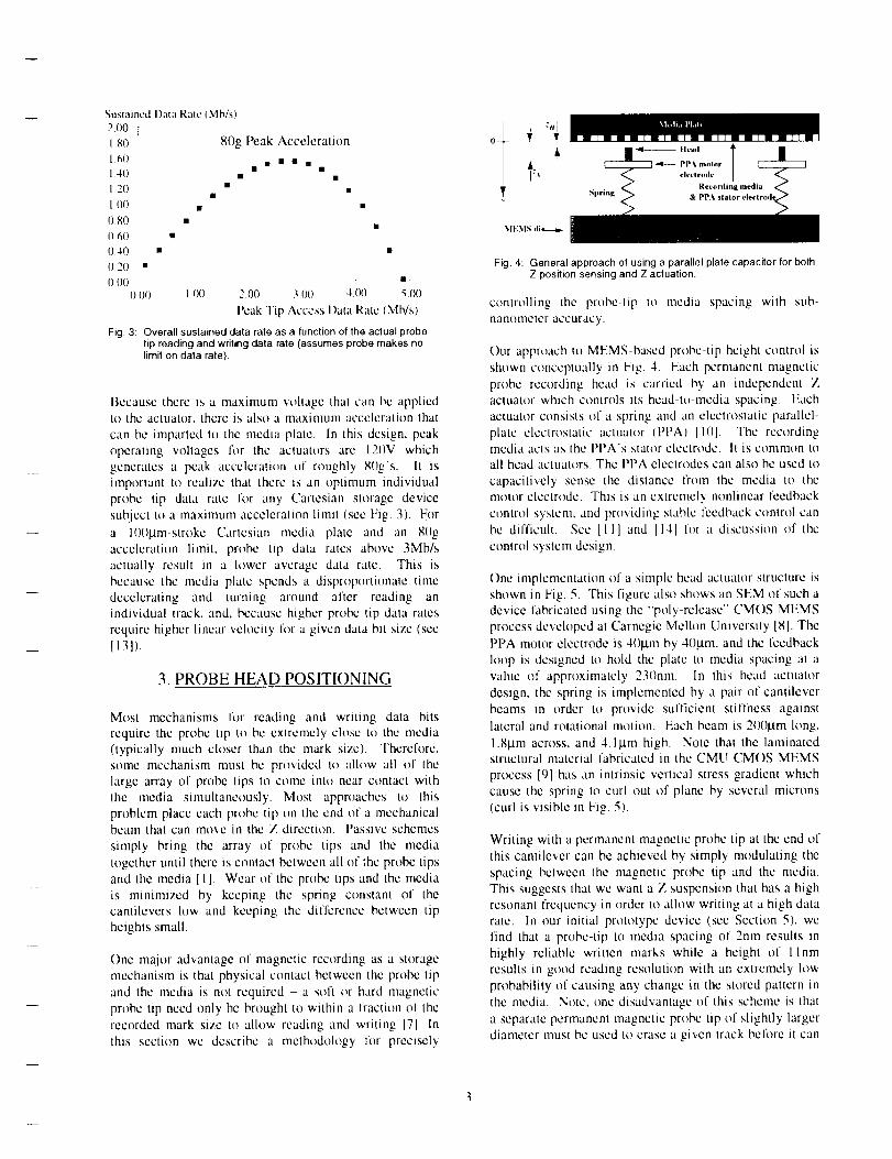
Fig. 3: Overall sustained data rate as a function of the actual probetip reading and writing data rate (assumes probe makes nolimit on data rate).
Because there is a maximum voltage that can bc applied
to the actuator, there is also a maximum acceleration that
can be imparted to the media plate. In this design, peak
operating w)ltages for the actuators are 120V which
generates a peak acceleration of roughl 3, 80g's. It is
important to realize that there is an optimum individual
probe tip data rate for any Cartesian storage device
subject to a maximum acceleration limit (see Fig. 3). For
a lOObtm-stroke Cartesian media plate and an 811g
acceleratitm limit, probe tip data rates above 3Mb/s
actually result in a lower average data rate. This is
because the media plate spends a disproportionate time
decelerating and turning around after reading an
individual track, and. because higher probe tip data rates
require higher linear velocity for a given data bit size (see
1131).
3. PROBE HEAD POSITIONING
Most mechanisms for reading and writing data bits
require the probe tip to be extremely close to the media
(typically much closer than the mark size). Therefore,
some mechanism must be provided to allow all of the
large array of probe tips to come into near contact with
the media simultaneously. Most approaches to this
problem place each probe tip on the end of a mechanical
beam that can move in the Z direction. Passive schemes
simply bring the array of probe tips and the media
together until there is contact between all of the probe tips
and the media [ 1 ]. Wear of the probe tips and the media
is minimized by keeping the spring constant of the
cantilevers low and keeping the difference between tip
heights small.
One major advantage of magnetic recording as a storage
mechanism is that physical contact between the probe tip
and the media is not required - a soft or hard magnetic
probe tip need only be brought to within a fraction of the
recorded mark sizc to allow reading and writing [71. In
this section we describe a methodology for preciscly
Ile_md 4
PPX motorz t electrode
T & PPASprin_
MEMS di w--_,.-
Fig. 4: General approach of using a parallel plate capacitor for bothZ position sensing and Z actuation,
controlling the probe-tip to media spacing with sub-
nanometer accuracy.
Our approach to MEMS-bascd probe-tip height control is
shown conceptually in Fig. 4. Each permanent magnetic
probe recording head is carried by an independent Z
actuator which controls its head-to-media spacing, t-ach
actuator consists of a spring and an electrostatic parallel-
plate clcctrostatic actuator (PPA) [10]. The recording
media acts as the Pl'A's stator electrode. It is common to
all head actuators. The PPA electrodes can also bc used to
capacitively sense the distance from the media to the
motor electrode. This is an extremely nonlincar feedback
control system, and providing stable feedback control can
be difficult. See I111 and 1141 for a discussion of the
control system design.
One implementation of a simple head actuator structure is
shown in Fig. 5. This figure also shows an SEM of such a
device fabricated using the "'poly-release" CM()S MEMS
process developed at Carnegie Mellon University [81, The
F'F'A motor electrode is 4llbtm by 4()btm. and the feedback
loop is designed to hold the plate to media spacing at a
value of approximately 230nm In this head actuator
design, the spring is implemented by a pair of cantilever
beams in order to provide sufficient stiffness against
lateral and rotational motion. Each beam is 200btm long,
I.Sbtm across, and 4.1btm high. Note that the laminatedstructural material fabricated in the CMU CMOS MEMS
process [9] has an intrinsic vertical stress gradient which
cause the spring to curl out of plane by several microns
(curl is visible in Fig. 5).
Writing with a permanent magnetic probe tip at the end of
this cantilever can be achieved by simply modulating the
spacing between the magnetic probe tip and the mcdia.
This suggests that wc want a Z suspension that has a high
resonant frequency in order to allow writing at a high data
rate. in our initial prototype device (scc Section 5), wc
find that a probe-tip to media spacing of 2nm results in
highly reliable written marks while a height of l lnm
results in good reading resolution with an cxtrcmely low
probability of causing any change in the storcd pattcrn in
the media. Note, one disadvantage of this scheme is that
a separate permancnt magnetic probe tip of slightly larger
diameter must be used to erase a given track before it can

be rewritten.Thereli_re,twoseparateZ mechanicalPP_. motor _ii¢
L t
Fig. 5: MEMS implementation of parallel plate capacitor for bothZ position sensing and Z actuation, Note, an SEM of sucha structure is shown at right without a head in place
suspensions must be able to access the same data area -
one for reading/writing and one for erasing. In essence, a
stripe of data on this devices (approximately 1()0() bit
positions long) is like a sector on a hard disk drive. It
must all be read or written at once.
When we are reading the data, we create what amounts to
a magnetic force microscope. The RMS equivalent
disturbance force noise due to the fronl end electronics
noise is approximately 38 17_/sqrl(Hz), which gives an
RMS input referred force noise floor that is about 12pN
assuming a 5()KHz bandwidth. For more details on the
noise lloor lk_r this sensor, see [ 141. Since the interaction
force between a permanent magnetic tip and a thin-film
magnetic media can be hundreds of pN, this means that
we can actually read the magnetic state of the media by
simply sensing the force the media exerts on the
permanent magnet read/write head. Nole, one other
source of disturbance is the Brownian noise associated
with the air between the actuator plate and the media. In
this case, we are assuming that we are operating in a near
vacuum and can neglect the Brownian noise contribution.
4. MAGNETIC PROBE RECORDING HEADS
Optimization of the design of permanent magnetic probe
heads interacting with a thin-film magnetic media would
leads to an extremely high aspect ratio cylinder of
permanent magnetic material. Fortunately, dropping the
aspect ratio down to 4:1 causes only a small drop in the
magnetic field at the tip of the probe.
In manufacturing, deposition of an array of permanent
magnet probe tips could be done using the Spindt tip
process [15] widely used in making field emission
displays with minimum effect on the other parts of the
structure. In this case we would have probe tips in the
shape of a cone, Alternatively, a combination of wide
area optical lithography with small area e-beam
lith_graphy can he used to cost effectively manufacture an
array of phomresist dots where tips are desired down to
5()nm in diameter [16J. l{y using this comhinati(m of
optical lithography and e-beam lithography to pattern a
magnetic thin film, 5{)nm diameter cylinders of a
permanent magnetic material with a height of l(l()nnT can
be created cost effectively [ 11],
5. SYSTEM PERFORMANCE SIMULATION
In order to assess the viahilit_ of the prop_sed storage
system, we created a detailed simulation thal includes the
effects of media noise, electronics noise. Brownian noise,
and manufacturing variations. We generate a distribution
of magnetic grain size. and orientation to match that of
today's commercial vertically oriented magnetic media.
Optimizing the selection of the magnetic probe tip
geometry for the best signal-to-noise ratio (SNR) resulted
in a cylindrical magnetic probe tip 40nm in diameter and
10(Into in height, The track pitch was 6grim and the bit
length (with run length coding) was l()()nm. For these
parameters, the simulation of 40110 recorded bits,
including the up and down movement of the probe tip
during writing and then a second pass scan for reading.
resulted in an RMS-Io-RMS SNR of 13 dB which is quite
sufficient for reliable signal detection.
6. CONCLUSIONS
Assuming a 2()_7, overhead fi)r error correction coding, the
track pitch and bit pitch determined for the initial
demonstration system results in approximatel_ 1.5 million
user bits being addressed by an individual magnetic probe
tip that scans over a 1001am by 100lure media area. The
overall system would consists of 6,4(1() of these individual
probe tip elements, resulting in a total storage capacity of
approximately 1Gbyte of user data on a 1.4cm x 1.4cm x
lmm 2 wafer silicon sandwich. The density of the
magnetic data stored on this media is limited by thermal
decay of the smaller magnetic grains over time. In our
simulations, we are assuming that a 1{) year lifetime is
required when we set the grain size. Fortunately,
researchers at companies that manufacture hard disk
drives are working hard to develop thermally stable media
with smaller grain sizes and as these developments
become available, we would expect the be able to increase
the density t)f data stored on MEMg-positioned magnetic-
probe-based mass storage devices.
7. ACKNOWLEDGEMENTS
We wish to specifically thank John Griffin, Arthur
l)avidson, Suresh Santhanam, 1)r. l,eon Abelmann, I)r.
Tamal Mukherlee, and the students and staff of both
CHIPS and lhe CMU MFMS research group who have
made many contributions to the work presented in this

paper.ThisresearchwassponsoredmparthytheNSFundergrantno.E('1)-89()7()68.inpartbyI)ARPAundertheAFRI,,AirForceMaterielCommand.USAF,underagreementF3()6(12-97-2-0323, in part by the National
Aeronautics and Space Administration, and in part by an
NSF Graduate Student t:ellowship. The United Slates
government has certain rights to this material. In
addition, we would like to acknowledge the equipment
donations by INTH, and IBM thai helped to support this
research. More information on this project can be found at
http://www.c hips.ece.cmu.edu.
8. REFERENCES
[11 M. I. l,ulwych, G. Cross. M. 1)espont, U. I)rechsler,
U. I)t, rig, W. tiaberle, H. Rothuizen, R. Shutz, R.
Widmer, (;. K. Binnig, P. Vettiger, "Millipede - A
highly-parallel dense scanning-probe-based data-
storage system," Dik, e._t or Technical Papers, IEEE
International Solid-State Circuits Conference, pp.126-127, Feb. 2()()1).
[21 S. Hoen, I'. Merchant, (L Koke, and J. Williams,
'+l{lectrostatic Surface 1)rives: theoretical
considerations and fabrication," Proceedings of the
9th Int. Con[i on Soli,t-State Sen_or_ and Actuators
(Transducers "97), Chicago, 1I,, pp 41-44, .lunc 1997.
[31 C. Morehousc, "A decadc away: atomic resolution
storage," sidebar in J. W. Toigo, "Awfiding a Data
Crunch." Scientifi_ American, May 2000.
[4] .l.J. Yao, S,C. Arney, and N.C MacDonald,
"'Fabrication of high freqt, cncy two-dimensional
nanoactuators for scanned probe devices", J.
Microelectromechanical Svstem,_, vol. 1, no. 1, pp.14-22, March 1992.
[5] T. Davis, "Realizing a completely micromechanical
data storage system," Proceedings of the IDEMA
DISKCON, Session 1, pp. 1-14, Santa Clara, CA, 21
Sept. 1999.
16] I,. R. Carley, J. A. Bain, (L K. Fcddcr, I) W Greve,
l). F, Guillou, M. S. C. l,u, T. Mukherjee, S.
Sanlhanam, l,. Abelmann, and S. Min, "Single-chip
computers with microclectromechanical systems-
based magnetic memory." J. qf Applied Phys., vol.
87, no. 9, pp. 6680-85, 1 May 2000.
[7] I,. Ahelmann, S. K Khizroev, 1). I,itvimw, J.-G. Zhu,
J. A. Bain, M. H. Kryder, K. Ramstock, and C.
I,otter, "Micromagnetic simulation of an ultrasmall
single-pole perpendicular write head," Journal eg
Applied Physics, vol. 87, no. 9, pp. 6636-38, May2OO{}.
[8[ I).F. Guillou, S. Santhanam and I,.R. Carley,
"I,aminated, sacrificial-poly MEMS technology instandard CM()S," Proc. Eurosensor,_ XIII, The
Hague, N[,, pp. 339-340, Sept. 12-15. 1999.
[9] G. K. Fedder, S. Santhanam, M.I,. Reed, S.C. Eagle,
I).F. Guillou, MS.-C. l,u and I,.R. Carley,
"laminated high-aspccl-ratio microstructures in a
cof_vcntional ('M()S process," Sensors and Actuator_
A, vol. 57 pp. 103-11(). 1996.
[10l(i, T. A. Km,,acs. Micromachined Tran,_duc'er_
Soureebook, New York. NY: McGraw-tlill, 1998.
[1111). F. (ku[lou, Design ol a MEMS-Based Data
Storage System. I'h.1). Thesis, 1)opt. of Electrical and
Comp. Eng, Carnegie Melhm Univ., Pittsburgh, PA.Dec. 2{)01.
[12IM. S. Kranz and (L K Fcdder, "Micromechanical
Vibratory Rate Gyroscopes Fabricated in
Conventional CM()S," Proc. of the Syrup. on Gvro
Technology, Stuttgart, Germany, pp. 30-3.8, Sept.16-17, 1997.
[13]Griffin, J. et. al. Modeling and Performance of
MEMS-Based Storage Devices, in Proceedings of
ACM SIGMETRICS '2000, ACM. New York, N.Y,
June 2()(){).
[14] I,. R. Carlcy, (keg Ganger, I)a_id Guillou, and David
Naglc. "System 1)esign Considerations for MEMS-
Actuated Magnetic Probe Based Mass Storage",
IEEE Transactions on Magnetics, vol. 37, no. 2, pp.657-662, March 20(11,
[15]C A. Spindt, C E. ilolland, A. Rosengreen, and I.
l?,rodie, Field-emitter arrays for vacuum
micmelectronics IEEE Trans. Electron Devices, vol.
38, no. l[},Oct 1991.
[161Y. Kondoh, J. Seeger, and P. Merchant, Fabrication
of nanoscale tungsten tip arrays for scanning probe
microscopy-based devices Journal o[
Microelectromechanical Sv,_'tems, Vol. 7, No. 4, pp.428-434, I)ec. 1998.

Integrating EEPROM, Resistor, Capacitor, PIN Diode,
Schottky Diode and Bipolar Modules into a 0.35 micron
CMOS process optimised for Low Voltage Applications.
John Ellis
Zarlink Semiconductor, Plymouth, Devon, U.K.
Abstract
We have integrated EEPRO,_, resistors,
capacitors, PL_ r diodes, Schottky diodes, an
isolated NPN &polar transistor and dual-
poly gate CMOS transistotw into a 0.35
micron technolo_'. This provides low
threshold voltage transistors for 1-3 V
battery operation, high voltage transistors
./'or EEPROM programming and a number
of passive components for mixed-signal
functions. Applications for this technolo_,
include Zarlink's medical products where
programmabili O, enables complex circuits
to be optimised .lot" individual customer
requirements.
1. Introduction
The integration of non-volatile memory
with passive components, transistors with a
low threshold voltage, PIN diodes,
Schottky diodes, high voltage transistors
and bipolar transistors offers a very diverse
range of options for custom, mixed-signal
products. We have integrated these into a
new 0.35 micron CMOS technology, called
ANV TM * for analogue, non-volatile, which
is compatible with our core 0.35 micron
digital process. It is intended for mixed
signal products in a range of low power
applications.
2. Quadruple Wells
The core 0.35 lam digital technology
begins with the field oxide formation. The
wells are implanted through the field oxide
using high energy implantation, but give
junction breakdown voltages of around 10-
12V, for circuitry operating at 3.3V. The
gate electrode on the core process is n-type
polysilicon. Two key requirements for the
new process were a low leakage, low
threshold voltage transistor, and secondly,
high voltage transistors for EEPROM
programming. We incorporated high
voltage wells in front of the field oxide,
which also use high energy allowing a
moderate thermal cycle to be used to drive
them. This has enabled us to provide
transistors with >I8V breakdown voltage
for EEPROM programming. The low
voltage transistors retain their normal well
implants post-field oxide. In this way the
new process steps are fully modular and do
not impact the core transistors.
To provide low threshold voltage
transistors we used N+ and P+ poly gatesfor the NMOS and PMOS transistors
respectively. The NMOS transistor is
identical to the one on the core digital
process but the PMOS is able to operate
* ANV is a trademark of Zarlink Semiconductor lnc
6

with 500 mV threshold, some 200 mV
lower than the partially-buried channel,
digital transistor. In addition, lower leakage
currents have been obtained. At longer
channels the P+ gate maintains a lower
threshold whereas the earlier N+ gate
exhibits an increase. Fig I illustrates the
new transistors. The PMOS device has
improved on the sub-threshold
characteristics compared with the NMOS.
Fig 2 compares the sub-threshold
characteristics of the high voltagetransistors.
NMZS _3S_n
, _o4 , ;
3 2 1 o 1 2 3
Fig. I l,ow Voltage Transistors
Vd=0.1, 3.3V: Vg=0... 3.3V
g
t gE 0"_
O_ 0 5
OE 0
OE -0
OE -0
50Y,OO, 'O OF+GO 5OE*O0
Vg (volts)
Fig. 2: lligh voltage transistors
Vd=0.1, 10V; Vg=0 ... 10V
3. EEPROM module
The EEPROM cell we integrated into the
low voltage process is a single-poly type
using a tunnel oxide window for Fowler-
Nordheim tunnelling for both writing and
erasing. This is an ideal solution for low
power non-volatile applications, and can be
supported from low current, on-chip
programming voltages. The single poly
process enables the EEPROM to be built as
a module and fully supports the Company's
double poly capacitor for analogue
applications.
The cell operates with 12-14V
programming voltage, typical write-erase
characteristics are shown in fig. 3.
7 00E-06
6 00E-06
5 00E-06
_" 400E-06
300E-06
200E-06
100E-06
000E+O0
/_ivate nt Vt
vandow=4 6V
4
0 1 2 3 4 5
Vg (volts)
erased
Fig. 3: EEPROM Erase and ProgrammingCharacteristics
4. Passive components
The number of resistors possible are so
extensive we only support a sub-set. For
battery operation from 1 to 3 V, and
analogue circuitry, a high value resistor is
desirable. We developed a 10 kohm/sq
resistor in polysilicon to meet this need.
Fig. 4 shows a typical resistor spread.
The resistor has a negative temperature
coefficient. At high voltages, above the
normal 3.3 V operating voltage, self-
heating can cause the resistance to drop.
For use in high voltage applications the
power must be limited to avoid this effect.
However, it may also serve as a
temperature indicator for sensor
applications.

2O
18
16
14
12
i ,o
6
4
2
0
Fig 4 High Value Resistor Distribution
In addition, several process resistors
arising from the P+ poly, N+ poly, buried N
layer and two sets of Nwells are supported
for designers to use. The high voltage,
silicide-protected I,DD regions are not
supported for design. Most resistors are
also available silicided, which tends to give
a similar value of about 3 ohms/sq for all.These are summarised in table 1.
P+ poly
N+ polyP+ diffusion
320
5O
9O
N+ diffusion 90
Nwell 1 kohm
10 kohmPoly 1 t liRes
Silicided (all) 3 (typ.)
Fable I: Supported Resistors
(ohms/sq unless stated otherwise)
Capacitors are available using the gate
oxide (4.5 fF/_tm2), high voltage gate oxide
(I.2 fF/_m 2) and a low parasitic, double
poly component (0.8fF/_tm-_).
5. Bipolar transistor
For some applications bipolar transistors
have advantages over MOS. Utilising the
deep, retrograde, high voltage Nwell as a
collector a reasonable quality' isolated NPN
transistor can be provided with the addition
of one base implant.
90
8O
70
6O
• " 40
30
20
10
0
1E-12 1E-10 1E-08 1E-06 00001 001
Log (Ic}
Fig. 5: Bipolar gain characteristics
(Emitter 0.6x0.6, poly defined)
6. Diodes
A fully isolated "P-I-N" diode in
polysilicon is available which uses the high
value resistor implant for the lightly doped
region, and has N+ and P+ end contact
diffusions. The breakdown voltage is
limited to approximately 7V but several
devices can be operated in series for higher
voltages.
A Schottky barrier diode is provided
using the titanium barrier metallisation
available in the process Fig. 6 shows
typical characteristics.

1 00E-04
9 00E-05
8 00E-05
7 00E-05
6 00E-05
5 00E-05,=,.
400E-05
3 00E-05
2 00E-05
100E-05
000E+O0
01 02 03 04 05
Vf (volts)
Fig. 6: Schottky Barrier Diode
(top: forward; bottom: reverse)
(minimum geometry)
001
0001
0 0001
1 E-05
--_ 1E-06
_1E-07
1E-08
1E-09
1E-I0
1E-11
i
5
Mr (volts)
10 15
7. Modular Flow
The ANV TM process is built using
Zarlink's 0.35 micron core digital
technology but has a number of fullymodular additions to form the new
components. The flow is illustrated in fig.
6, showing how the new modules may be
used flexibly.
Prior to growing the field oxide, high
voltage wells are implanted and driven.
After growing the field oxide, the standard
low-voltage (digital) wells are implanted. A
number of masking stages are used to
define the EEPROM coupling diffusion,
dual gate oxides, bipolar and poly gate
material. After poly 1 the only additional
high voltage I--wells
EEPROMBuried gateTunnel oxide
Bipolarmodule
HRes Res stor
low voltagewells
Ngate, Pgate
P2 Capacitor
Fig. 7: Modularised Flow
module is for high voltage LDD regions.
Poly 2 and low voltage LDDs are standard.
8. Applications
This technology is suitable for many low
power applications. Test chips for
logic/DSP and memory are shown in fig. 8
(a) and (b). Some applications operate from
single cells and low power is key to
extending the battery life.
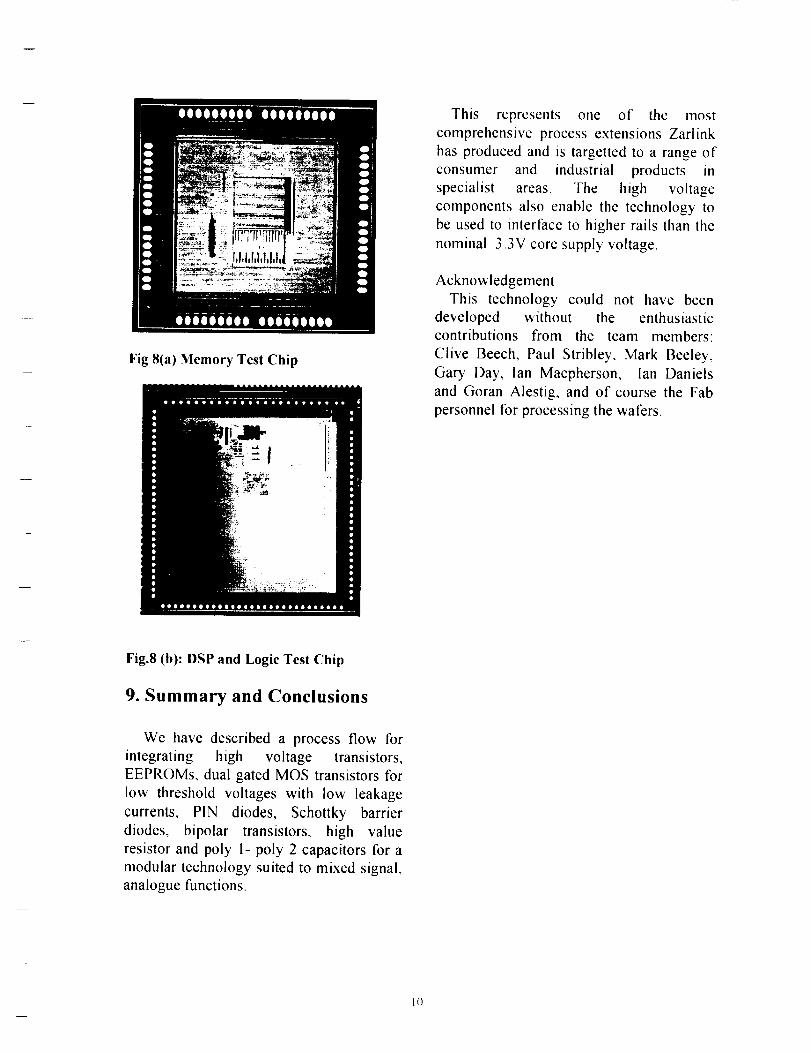
Fig 8(a) Memory Test Chip
This represents one of the most
comprehensive process extensions Zarlink
has produced and is targetted to a range of
consumer and industrial products in
specialist areas. The high voltage
components also enable the technology to
be used to interface to higher rails than the
nominal 3,3V core supply voltage.
Acknowledgement
This technology could not have been
developed without the enthusiastic
contributions from the team members:
Clive Beech, Paul Stribley, Mark Beeley,
Gary Day, lan Macpherson, lan Daniels
and Goran Alestig, and of course the Fab
personnel for processing the wafers.
Fig.8 (b): DSP and Logic Test Chip
9. Summary and Conclusions
We have described a process flow for
integrating high voltage transistors,
EEPROMs, dual gated MOS transistors for
low threshold voltages with low leakage
currents, PIN diodes, Schottky barrier
diodes, bipolar transistors, high value
resistor and poly 1- poly 2 capacitors for a
modular technology suited to mixed signal,
analogue functions.
10
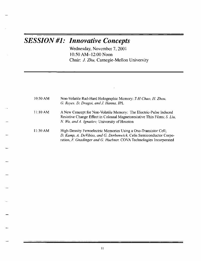
SESSION #1: Innovative ConceptsWednesday, November 7, 2001
10:50 AM-12:00 Noon
Chair: J. Zhu, Carnegie-Mellon University
10:50 AM
ll:10AM
11:30 AM
Non-Volatile Rad-Hard Holographic Memory; T-H Chao, H. Zhou,
G. Reyes, D. Dragoi, and J. Hanna, JPL
A New Concept for Non-Volatile Memory: The Electric-Pulse Induced
Resistive Change Effect in Colossal Magnetoresistive Thin Films; S. Liu,
N. Wu, and A. Ignatiev; University of Houston
High-Density Ferroelectric Memories Using a One-Transistor Cell;
D. Kamp, A. DeVibiss, and G. Derbenwick, Celis Semiconductor Corpo-
ration, F. Gnadinger and G. Huebner, COVA Technologies Incorporated
I1
Nonvolatile Rad-Hard Holographic Memory
Tien-t Isin Chao, I lanying Zhou, George Reyes, l)anut l)ragoi, and Jay ttanna
Jet Propulsion I.aboratoryCalifonia Institute of Technology,
4800 Oak Grove Drive
Pasadena, CA 91109
ABSTRACT
We are investigating a nonvolatile radiation-hardened (rad-hard)holographic memory
technology. Recently, a compact holographic data storage (CHDS) breadboard utilizing aninnovative Electro-optic scanner has been built and demonstrated for high-speed holographic data
storage and retrieval. The successfiil integration of this holographic memory breadboard has
paved the way for follow-on radiation resistance test of the photoreffactive (PR) ct3'stal,Fe:l,iNbO_ Wc have also started the investigation of using 2-photon PR crystals that are doubly
doped with atoms of iron group (Ti, Cr, Mn, Cu) and of rare-earth group (Nd, Tb) for nonvolatile
holographic recordings.
!. INTRODIICTION
NASA's fiiture missions would require massive high-speed onboard data storage
capability II1 This is a particularly challenging technology' isstie fbr long-life, deep spacemissions. The memory technology required to support these missions have to be rad-hard and
nonvolatile (i.e. no loss of stored data after power switched off). Nonvolatile memory is critical to
spacecraft's abili_' to survive fault conditions (i.e. no loss in stored science data when spacecraftenters the "safe mode") and autonomously recover from them. In addition, this nonvolatile
memou' has to be rad-hard to survive the stringent space environment (e.g. very high radiation
around Europa where radiation exceeding I Mrad) It should also operate effectively andefficiently for a vet3' long time ( 10 years), and sustain al least a billion ( 10 t2) write cycles
Current technology, as driven by the personal computer and commercial electronics
market, is focusing on the development of various incarnations of Static Randorn Access Memory
(SRAM), Dynamic Random Access Memory (DRAM), and Flash memories [2, 3]. Both DRAMand SRAM are volatde. The Flash memory, being nonvolatile, is rapidly gaining popularity
Densities of flash memory of 512 Mbits per die exist today. However, Flash memory is presently
faced with two insurmountable limitations: 1) poor radiation-resistance (due to simplification inpower circnitry tbr ultra-high density package); and 2) Limited endurance tbreakdown after
repeated read/write cycles).
JPL, tinder sponsorship from NASA Earth Science Technology' Office, is currently
developing a high-density, nonvolatile and rad-hard Compact !tolographic Data Storage (CHDS)
system to enable large-capacity, high-speed, low power consumption, and read/write of data for
potential commercial and NASA space applications [4,5]. The CHDS stores data in the fonn of
holograms inside a photorefractive (PR) crystal. In operation, pages of holograms would berecorded and retrieved with random access and high-speed Since these holographically recorded
images are stored m three dimensions and uniformly spread out throughout the entire recordingvolume, massive redundancy is built into the holograms, and the stored data would not stiffer
from imperfections m the media or point defects This massive redundancy forms the basis for
12

radiation-resistanceOntheotherband,recentadvancesinnewphotorefractivematerialresearchmakeit possibletoextendthelifetimeof thehologramsrecordedin PRc_'stalsfrommonthstodecadesor longer[6].Thenonvolatile,rad-hardcharacteristicsof theholographicmemo_'willprovidea revolutionarymemo_,technologyto enhancethedatastoragecapabilityfor allNASA'sEarth Science Missions.
In this paper, we will first briefly report the most recent progress in developing this
CI[DS at JPI,. Ongoing and future research effort m developing nonvolatile tad-had
photorefractive recording materials will then be discussed m detail
!!. CHDS BREADBOARD DEVELOPMENT AND EXPERIMENTAL
DEMONSTRATION
JPI. has recently built a fidly fimctional book-size Cttl)S breadboard using liquid c_stal SI.M as
beam steering device [4,5]. Figure l a shows the CHDS architecture, and Fig. l b is a photograph ofthe CttDS breadboard. In this breadboard we have implemented a I-D scanning scheme using a
single beam steering SLM (from Boulder Nonlinear System, Inc ) which is capable of recording128 resolvable holograms to date. A LabView based system controller has been developed to
perfonn holographic data recording/retrieval in an autonomous manner
We have successfully perfonned hologram recording/retrieval demonstrations nsmg this
breadboard. Dnnng this experiment, we have utilized a sequence of grayscale images of the near
earth asteroid, Toutatis, as the input. A few retrieved images from the holograms recorded in the
LiNbO_, presenting the Toutatis viewed in several aspect angles, are shown m Figure 2.
In the next step, a pair of this BSSLM will be cascaded to enable 2-D scanning of the referencebeam to increase the number of stored holograms This 2-D beam multiplexing would result in a
total of 11,520 resolvable scanning angles. Thus it will enable the storage of more than 11,000
pages of holographic data within a ]-cm _ volume of a PR crystal. The total storage capacity,
when using a 1000xl000 pixel size SI,M as input device, would exceed 10 Gbs. Further increasethe input flame size (e.g. 5000x5000 pixels) would further increase the memory size to 250 Gbs.
Photodetector
Arra_
Laser Diode _1
|, I_V '4"-
...................................................................!Readout ModuleWrite Module
Figure
a b
l a. System schematic architecture of an Advanced Holographic Memo_'
I b A book-sized CHDS breadboard under development at JPI.
13

Thepotentialof stackingamultipleof ve_,compactholographicmemor3_cubesona memor3'card(e.g.10x 10cubesoneachcard)will provideupto I terabitsstoragecapacitypercardThetransferraterangesfrom200Gbs/sec(withnematicliquidc_'stalBSSI,M)to2000See/see(withfcrroelectricliquid c_'stalBSSS1,M).In summary,primaryadvantagesof this holographicmemorysysteminclude:highstoragedensity,hightransferratevia randomlyaccessibleE-Obeamsteenng,compactandraggedness, low voltage and low power consumption.
Figure 2 Experimental results showing retrieved laolographic images of asteroid Toutatis
!11. NONVOI,ATILE PHOTOREFRACTIVE MATERIAL
Recently, technology breakthrough in extending storage lifetime of photorefractive memo_' frommonths to decades or longer have been reported by researchers at Caltech and elsewhere A new
Wpe of two-photon recording material, doubly doped Fe:Mn:LiNbO._, has been developed. Thismaterial possesses a deep traps partially filled with electronics and a shallow (intermediate) traps
to trap photo-generated electrons with very long lifetime. Doubly doped extrinsic dopants (Fe z ,
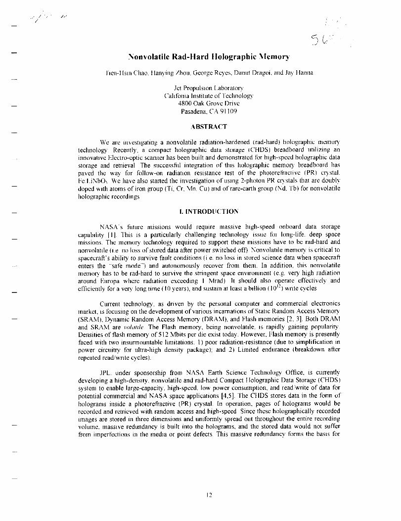
Mn 2) would provide this intermediate state. As illustrated in Figure 3: During recording, a first
photon (from an ultraviolet light source) is used to excite an electron form the Valence band to anintermediate state A hologram wntmg photon is then used to bring the electron up to the
Conduction band. The electron will then migrate and get trapped to record the interferencepattern During readout, the readout beam will readout the hologram but is with insufficient
energy to elevate the electron to the conduction band Hence the stored hologram will not be
erased during readout
More recently, more doping ions from the iron group ions (Ti, Cr, Mn, Cu) [6] and the rare-earth
group iotas (Nd, Tb) [7] have been investigated for nonvolatile performance in a l.iNbO3 crystal. To
date, it has been reported that doubly doped Cr:Cu:LiNbO_ as well as Fe: Tb:ViNbO_ are effective mnonvolatile holographic recordings.
14
inter_ hv2
statehvl
Donor site
Trap Intermediatesite state
Donor site
hv2
Acceptorsite
a. Recording b. Readout
Figure 3. Two-photon nonvolatile hologram a) recording and b) reade
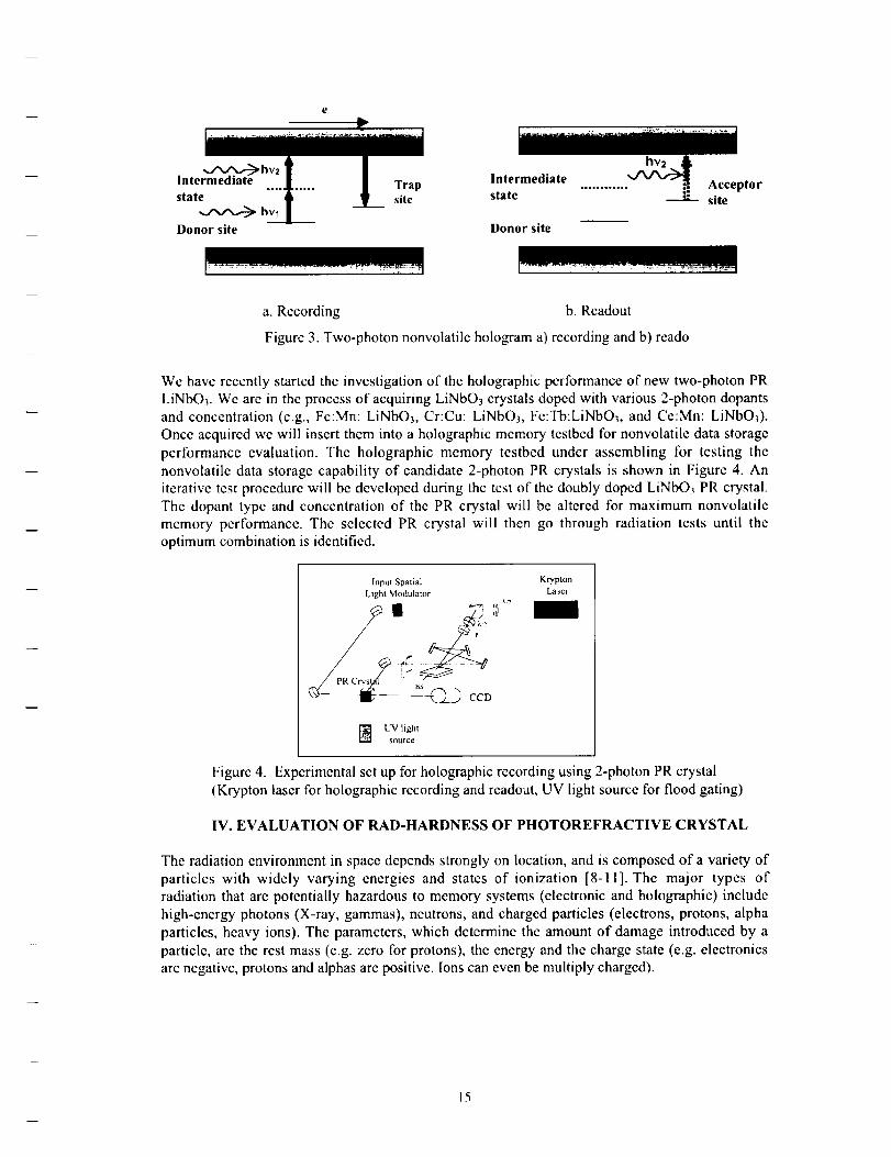
We have recently started the investigation of the holographic performance of new two-photon PR
LiNbO3. We are in the process of acquiring LiNbO3 crystals doped with various 2-photon dopants
and concentration (e.g., Fc:Mn: LiNbO3, Cr:Cu: LiNbO_, Fc:Tb:LiNbO_, and Ce:Mn: LiNbO3).
Once acquired we will insert them into a holographic memory testbed for nonvolatile data storage
performance evaluation. The holographic memory testbed under assembling for testing the
nonvolatile data storage capability of candidate 2-photon PR crystals is shown in Figure 4. An
iterative test procedure will be developed during the test of the doubly doped LiNbO3 PR crystal.
The dopant type and concentration of the PR crystal will be altered for maximum nonvolatile
memory performance. The selected PR crystal will then go through radiation tests until the
optimum combination is identified.
Input Spatial
Light Modulator
Krypton
Laser
k2
UV lightSOIIICd
Figure 4. Experimental set up for holographic recording using 2-photon PR crystal
(Krypton laser for holographic recording and readout, UV light source for flood gating)
IV. EVALUATION OF RAD-HARDNESS OF PHOTOREFRACTIVE CRYSTAL
The radiation environment in space depends strongly on location, and is composed of a variety of
particles with widely varying energies and states of ionization [8-11]. The major types of
radiation that are potentially hazardous to memory systems (electronic and holographic) include
high-energy photons (X-ray, gammas), neutrons, and charged particles (electrons, protons, alpha
particles, heavy ions). The parameters, which determine the amount of damage introduced by a
particle, are the rest mass (e.g. zero for protons), the energy and the charge state (e.g. electronics
are negative, protons and alphas are positive. Ions can even be multiply charged).
15

Theradiationill spacehasa degradingeffecton tile microelectronicdevices.Forexample.neutronsbombardmentsofSiatomswillconverttheln into Plaosphorous/Neutron TransmutationEffect) that will adversely affected the performance of electronics. The radiation effect on the
I,iNbO_, the most important PR material, has been partially investigated ill literature, hi generalthe degrading effect of radiation on l,ithium Niobate is a fimction of the type of the dopants andof the radiation dose [8-II ].
The primary radiation effects on PR cryslals due to all types of aforemenlioned radiation sources
include variations m refraction index, spectral absorption (coloring), and change of density{volume expansion and striation). A summary of tile previous study of the radiation effects on thedoped LiNbO_ is shown m Table II
Table !. Radiation types and their damages to doped LiNb03 holographic material
Types of damages
Source of Radiation
X-rays, y-rays
Neutrons/charged
particles
Refractive index
fan,,) changes
A(n,,) increases withdose
Decrease with dose
Density changes
Nolle
Vohune increases at
very high nuclear
deposited enerb, y
Spectral absorption
Spectral absorption ill
blue spectral regionobserved
NOlle
The preliminary results of radiation test of doped LiNbO_ crystal have shown enconraging results
that those damages occnrred in orders of magnitude higher dose than that of the electronics.
These tests indicated that rad-hard holographic memory could be developed using iron(s) dopedLiNbO_ PR crystal
We will conduct a comprehensive radiation test of several doubly doped LiNbO_ PR crystals.Specifically, we will measure the following key PR material parameters before and after the
radiation tests: photoreffactive sensitivity, recording time-constant, and material dynamic range(or maximum refractive index change). In addition, other material properties, such as optical
uniformity, scattering noise, etc. would also be measured to evahlate the qualib' of tile retrievedholographic data
CONCI,USION
In summary, we have built a fully fimctional book-size CHDS breadboard using liquidcrystal SLM as beam steering device and demonstrated the recording and retrieval of holograms
with high quality. Radiation resistance test of the PR crystal LiNbO3 is under way. In addition,we have also started the investigation of new 2-photon PR crystals for nonvolatile holographicrecording
ACKNOWLEDGMENT
The research described in this paper was carried out by the Jet Propulsion Laboratory, Califonlia
Institute of Technology, under a contract with the National Aeronautics and SpaceAdministration.
16

REFERENCES
1 K I=Strauss,T. l)aud,"'Overviewof radiationtolerantunlimiledwritecyclenonvolatilememory".Proceeding of IEEE Aerospace Conference 2000.
2 W. Schobcr, F. Lansing, K Wilson, and E Webb, "ltigh Data Rate Instrtunen! Study", JPI.
publication 99-4.3 A K Shanna. Semiconductor memories, IEEE Press, 1996
4 T f I Chao, I I Zhou, and G Reyes, "lligh-density holographic memor) and its applications to
optical pattern recognition," proceedings of SPIE on ISOM.ODS'99 VOL 3864, pp 181-183
July. 19995 _I H (,hao. tt Zhou and G Reyes, "Advanced compact holographic data storage system,"
Proceedings of Non-volatile memory technology symposium 2000. pp 100-105, November.2000
6 K Buse, A ._dibi, and I) Psaltis, '_Non-Volatile lfolographic Storage m I)oubl) Doped l.ithium
Niobate Crystals," Nature 393, 665668 (1998)7 M I.ee, S Takekawa, Y. Furukawa, K. Kitamura, and tt Hatano, "Nonvolatile and quasi-
nonvolatile holographic recording in near-stoichiometric lithiurn niobtae doubly-doped with Tb
and Fe". E/VIRS 200(I [n{emational Conference on Electronic Materials, Strasbourg France (Max
2000)8 R Yu Azimzadc. A Kh. Zeinally, 1. S Kogan, and A l. Timofeev. "Effect of gama radiation
on hologram recording", Sov. Phys Tech Phys 24(9), p.1143, 1979
9 T R Volk, S A. Shramchenko, and k A Shuvalov, "Changes in birefringence of LiNbO3
crystals undel the influence of x-rays (x-ra) refraction effect)" Soy Phys Solid State.
28( 12).p2135-.2138 198410 S B Ubizskii. A O Matkovskii, N A Mironova-Ulmane, V Skvortsova A Suchocki, Y
A Zhydachevskii. P Potera. "Radiation displacement detect formation in some complexoxide c_stals", J Nucl Instr and Meth in Phys Res B 166-167 (2000) 40-46.
11 G. Gotz, "Radiation effects in optoelectronic materials", Radiation Effects, 98_ pp 189-210,1986
17

/,'
i /]
A New Concept for Non-Volatile Memory: The
Electric-Pulse Induced Resistive Change Effect in
Colossal Magnetoresistive Thin Films
S.Q. Liu, N. J. Wu and A. lgnatiev
Space Vacuum Epitaxy ('enter
University of tlouslon
Houston, TX 77204-5004
713-743-3621
I.qnatiev_,UH.edu
I. Abstract
A novel electric pulse-induced resistive
change (EPIR) effect has been found in thin film
colossal magnetoresistive (CMR) materials, and
has shown promise for the development of
resistive, nonvolatile memory. The EPIR effect
is induced by the application of low voltage (<
4V) and short duration (< 20ns) electrical
pulses across a thin film sample of a CMR
material at room temperature and under no
applied magnetic field. The pulse can directlyeither increase or decrease the resistance of the
thin film sample depending on pul_ polarity.
The sample resistance change has been shown
to be over two orders of magnitude, and is
nonvolatile after pulsing. The sample resistance
can alto be changed through multiple levels - as
many as 50 have been shown. Such a device
can provide a way for the development of a
new kind of nonvolatile multiple-valued memory
with high density, fast write/read speed, low
power-consumption and potential high
radiation-hardness.
II. Introduction
A great amount of effort is being
applied to the development of nonvolatile
memories (NVM) in response to a huge
demand for non-powered high-density data
storage [I,2]. Recently more and more interest
has moved to two-terminal resistive-type
devices, including the utilization of crystalline-
amorphous phase transition effect [3],
ferroelectric diode effect [2], the dielectric
dispersion effect [4], and magnetoresistive
memories [5]. Although NVM innovation and
technology are experiencing great growth, new
memory concept and technologies are needed
to support the rigid challenges to the
requirements: low power and low voltage for
reading and writing, non-volatility with infinite
retentivity, fast, inexpensive, radiation-hard, and
infinitely rewritable.
The hysteretic behavior of the resistivity
of the colossal magnetoresistance (CMR)
materials under high magnetic fields and low
temperatures has incited interest to develop
new nonvolatile memory devices in this
materials system [6,7]. However, the high
magnetic fields and the low operating
temperatures are hindrances to applications.
Much effort has been expended to overcome
the_ difficulties including utilizing the extnnsic
effects of grain boundaries [8], field focusing
[9], and the intrinsic effect of tunneling [10,11].
However, only small changes in resistance of
from 2 to 20% were obtained.
We have recently found that an electric
field can alto induce resistance change in CMR
materials at room temperature and under no
18
applied magnetic field [12]. By applying short
electrical pulses with moderate voltage to the
magnetoresisnve thin films, a new resistive effect
with a large room-temperature nonvolatile
resistance change ratio (>20,000%) has been
achieved. Based on this electrically variable and
reversible resistance change effect, we report
here a new nonvolatile, rewritable binary and
mulu-valued memory elements driven by
electrical field, and made of thin
magnetoresistivc material which can be read
and written randomly at high speeds. More than
50 nonvolatile resistance levels (bit level) have
been demonstrated in a simple two-terminal
storage element with no requirement for initial
forming or poling.
111.Device Fabrication
l)r_; 7(% _Mn()_ (PCMO) thin films of
thmkness range of 300nm-800nm were grown
epitaxially by pulsed laser deposition (PI,D) on
atomically ordered Yba2CmOv_, (YBCO) and
platinum substrates. The YBCO and Pt films
were epitaxially grown by pulse laser deposition
(PLD) and e-beam vaporization respectively on
the (100) LaAIO_ (LAO) substrates, and were
used as the bottom electrodes and the atomic
templates for PCMO epitaxial growth. The
epitaxial PCMO films were nominally grown at
700"C-750°(7 in an atmosphere of ~200
mTorr of flowing oxygen, and then were cooled
to room temperature under one atmosphere of
oxygen. Pattemed metal (Ag, Au or l°t)
contacts were fabricated on top of the PCMO,
YBCO and base-Pt layers by room
temperature sputtering.
IV. Results And Discussion
Write and erase electrical pulses were
applied to the samples through the metal
contact pads on the top PCMO and the bottom
YBCO or Pt layers. Applied pulses with
amplitude and duration values over a set of
values called "the start threshold values"
resulted in change in sample resistance. The
start threshold values depend on the film
thickness and composition, and are nominally
1V-3V at pulse widths of ~ 10ns or less. Pulses
with negative polarity (negative pulse applied to
the top electrode on PCMO film) resulted in an
increase in ,sample resistance to a high
saturation value. Pulses of opposite polarity'
resulted in a decrease in sample resistance to a
low saturation value. The high and low
,saturation values depend on the applied pulse
amplitude and duration which must be below
another set of values called "the break
threshold values", over which the sample will be
damaged. When the amplitude and duration of
the pulses are between the "start" and "break"
threshold values and are selected suitably, the
sample resistance can be switched between
binary states by single pulse or multi-pulses, as
well as can be changed in a gradual and
stepwlsc manner resulting m multitudinous
intermediate hysteresis resistance levels.
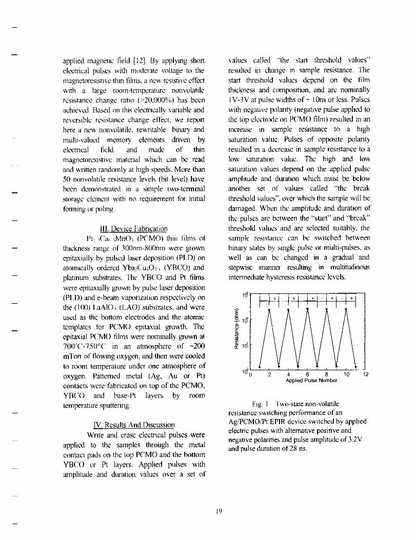
g_I_
oE
r, _d
lO0 12
i"-+ • i+i
_1 i i i i i
2 4 6 8 10
Applied Pulse Number
Fig. 1 Two-state non-volatile
resistance switching performance of an
Ag/PCMO/Pt EPIR device switched by applied
electric pulses with alternative positive and
negative polarities and pulse amplitude of 3.2V
and pulse duration of 28 ns.
19
Switchingperformanceby singlepulsefor an Ag/PCM()(100)/Pt(100)two-terminaldeviceis shownin Fig. I, wherethethicknessof theactivePCMOlayeris 300rim,andthepulseamplitudeis 3.2V with a durationof28ns.At roomtemperature,thepositivepulseinducesa low nonvolatileresistancestate,andthenegativepulseinducesa highnonvolatileresistancestatcindicatingidealtwo-statelogicbehavior.An EPIR ratio, defined as: AR/RMIN =
(RM,xx RMIN),_XMIN, where RMAXand RMENare
the maximum and minimum nonvolatile
resistances induced by write and erase pulses,
can be used to describe the device resistance
change. The induced EPIR ratio of this device is
more than 20,000% at room temperature.
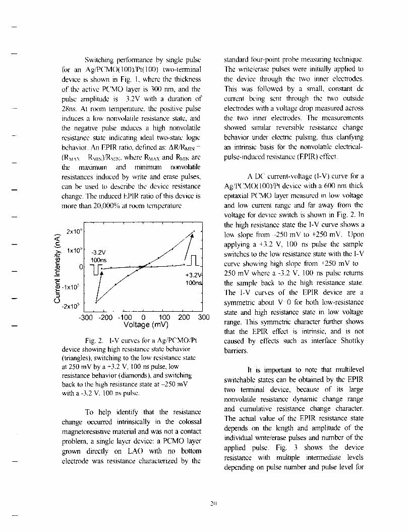
<t"
v
O9
(D
c"
t-0at-
cO
2x10 "_
lx10 s
0
-lx10 _'
-2x10si
-300
T I ' _ I 1
100ns
+3.2V.lOOns
I I t , I , I +
-200 -100 0 100 200Voltage (mV)
Fig. 2. I-V curves for a Ag/PCMO/Pt
device showing high resistance state behavior
(triangles), switching to the low resistance state
at 250 mV by a +3.2 V, 100 ns pulse, low
resistance behavior (diamonds), and switching
back to the high resistance state at -250 mV
with a -3.2 V, 100 ns pulse+
300
To help identify that the resistance
change occurred intrinsically in the colossal
magnetoresistive material and was not a contact
problem, a single layer device: a PCMO layer
grown directly on LAO with no bottom
electrode was resistance characterized by the
standard four-point probe measuring technique.
11ae write/erase pulses were initially applied to
the device through the two inner electrodes.
This was fbllowed by a small, constant dc
current being sent through the two outside
electrodes with a voltage drop measured across
the two inner electrodes. The measurements
showed similar reversible resistance change
behavior under electric pulsing, thus clarifying
an intrinsic basis l'br thc nonvolatile electrical-
pulse-induced resistance (EPIR) effect.
A D(" current-voltage (i-V) curve for a
Ag/PCMO( 100)/Pt device with a 600 nm thick
epitaxial PCMO layer measured in low voltage
and low current range and far away from the
voltage for device switch is shown in Fig. 2. In
the high resistance state the I-V curve shows a
low slope from 250 mV to _-250 mV. Upon
applying a +3.2 V, 100 ns pulse the sample
switches to the low resistance state with the I-V
curve showing high slope from _250 mV to
250 mV where a -3.2 V, 100 ns pulse returns
the sample back to the high resistance state.
The I-V curves of the EPIR device are a
symmetric about V O for both low-resistance
state and high resistance state in low voltage
range. This symmetric character further shows
that the EPIR effect is intrinsic, and is not
caused by effects such as interface Shottky
barriers.
It is important to note that multilevel
switchable states can be obtained by the EPIR
two terminal device, because of its large
nonvolatile resistance dynamic change range
and cumulative resistance change character.
The actual value of the EPIR resistance state
depends on the length and amplitude of the
individual write/erase pulses and number of the
applied pulse. Fig. 3 shows the device
resistance with multiple intermediate levels
depending on pulse number and pulse level for
2[)

a device with Ag/P(,M()(ll)O)/c-oriented
YB(;() structure. Each resistance level could
corrcsponds to a specific state of memory, and
thus Fig. 3 clearly shows that more than 50nonvolatile resistance levels can be stored m a
simple two terminal storage element. The insert
m Figure 3 also shows that with appropriate
pulse numbers and pulse levels and polarities,
any resistance state of the device is attainable.
It is projected that a larger number of resistance
levels will be able to be obtained upon
optimization of the resistance element
heterostructure and the pulsing and sampling
process
1200C
1000C
80000
6000
(D4000
2000
_ _l_
- I I" I " I " I" I "
i
0
L, I i I I I i i i I , I
10 20 30 40 50
Applied Pulse
Fig. 3. The resistance change versus
write pulse number for aPr0vCal_ _MnO3/Yba2CmO7 device. The write
pulse duration was lOOns and the pulse amplitudewas varied from 5V to 10V in increments of
-1V. 53 discrete resistance steps can be seen forthis sample. The insert shows the possibility of
ramping sample resistance up and down with
appropriate number of pulses and pulse heights.
An endurance test has shown that the
present experimental devices, which have not
yet been optimized for performance, canwithstand much more than 10s resistance
switches. Fig. 4 shows the results for a
PCMO/YBCO device to which more than
100,000 pulses of 12V and 80ns were applied
at a frequency of 1011z. llae EPIR ratio
approaches a non-zero saturation value of
about 50% of the maximum value at high pulse
numbers with this saturation behavior indicating
the possibility' of much higher pulse numbers
I'hc changed resistance value, that is, a given
resistance memory, state, was also stable withtime with a resistance shift of less than 1°4, over
2.5× I0 _ seconds
O
t_
n-g_I..U
IDN
EO
z
100
80
60
40
20
0
10 _
...... , ........ 4 .... ,,,,I _ -_a..._a..a4_
102 103 104 10 _
Applied Pulse Number
Fig. 4. A normalized EPIR ratio versus
write and erase pulse number for a
Pr07Ca0_MnO_/Yba2Cu307 device cycled atroom temperature. Note the plateau behavior
with pulse number projecting good resistance
ration stability at much higher pulse numbersthan shown.
As the present time devices are aimed
at the experimental demonstration of the initial
operation of an electrical-pulse-induced
resistance change device, and thus they have
not yet been fabricated in small size. The topelectrode contacts for the devices were either
2001am or 5001am diameter. As a result, there
are possibilities to improve device performance
by decreasing device size to micron or
submicron levels. For example, when the device
becomes smaller the write energy is expected to
be reduced. For a 500 lam device with write
voltage of 5V and resistance of 200f_ the write
energy is ~2nJ. This is already lower than rome
21

present CMOS-related devices [1] Thereduction of device area for the EPIR device
will increase its resistance resulting in a further
decrease in write energy.It is well to note that the EPIR device
reported here is not seen to depend on the
storing ol charge as most semiconductol
nonvolatile memories do [13]. l he EPlR effec!
is believed to depend on fizrromagnetic cluster
arrangements of polarons and/or residual Jahn-
Teller distorted Mn_'O :' stripes (JTS) in the thin
PCM() films which are accompanied by lattice
distortions and phase separation [14-16]. Such
cooperative phenomena are not expected to be
greatly affected by high energy particles, and
hence the EPIR devices should be radiation
hard.
V. Conclusion
A novel kind of rewritable, non-volatile
resistance memory has been demonstrated
experimentally in perovskite oxide thin films,
particularly CMR material films, based on
electrically-induced resistance changes at rc-_m
temperature. The electrically switched
resistance devices have shown two-state
behavior at switching voltages of <4V, and
because of the large resistance change
capability and cumulative behavior, an EPIR
memory element with a simple two terminal
structure has shown a storage ability of morethan 50 discrete nonvolatile levels. The data
write times are less than 20ns, and the write
energy is lower than 2nJ. Preliminary endurancetests have shown that the devices can withstand
much more than 10s resistance switching cycles.
The EPIR effect is very different from
the previously known resistive memory effects
such as the ferroelectnc diode effect, the
semiconductor crystalline-amorphous phase
transition effect, and the dielectric dispersion
effect, and is projected to be radiation hard.
The mechanism responsible for the effect is
currently being investigated, however, it is clear
that the EPIR effect is a new physical
phenomenon which provides the possibility, to
built a solid state, electrically operated, directly
overwntablc, low' excitation energy, ve_' fS.st
switching, nonvolatile, and multileveled high
density resistive memory system.
VII. Acknowledgments
]'his work was supported in part by
NASA, the Texas Advanced Research
Program, the R. A. Welch Foundation and
Sharp Laboratories of America, Inc
Vll. References
[1] M. I)ax, "The non-volatile memory
challenge," Semiconductor International, p 84.
Sept. 1997.
[2] M. Okano, and Y. Watanabe, "Nonvolatile
programmable two-terminal diodes using a
ferroelectnc semiconductor," Appl. Phys Lett.,
76, 233 (2000).
[31 W. D. Buckley, "Filament-type memory
semiconductor device and method of making
the same," U.S. Patent, No. 3886577, (1975).
[4] M. J. Rose, J. Hajto, P. G. LeComber, S. M.
Gage, W. K. Choi, A. J. Snell, and A. E. Owen,
"Amorphous silicon analogue memory devices," J.
Non-Cryst. Solids 115, 168 (1989).
[5] G. A. Prinz, "Magnemelectronics,"
Science, 282, 1660 (1998).
[6] G. C. Xiong, Q. Li, H. L. Ju, S. M. Bhagat,
S. E. Lofland, R. L. Greene, and T.
Venkatesan, "Giant magnetoresistive memory
effect in N& vSra0 _MnOz films," Appl. Phys.
Lett., 67, 3031 (1995).
[7] Y. Tomioka, A. Asamitsu, tt. Kuwahara,

Y. Moritomo,andY. lokura,"Magnetic-field-inducedmetal-insulatorphenomenain PrL,('a_Mn()_ with controlled change-ordering
instability," Phys. Rex,. B, 51. R1689 (1996).
18[ S t'. Isaac, N. 1) Mathur. ,1. t t-veils,
and M (i Blamire "'Magnetoresistance ol
artificial l,a_j 7Sr,:,_Mn(); grain boundaries as a
function of misorientalion angle," Appl Phys
l_ctl., 72, 2038 (1998).
19[ It Y Hwang, S-W. ('heong and B.
Batlogg, "Enhancing the low field
magnetoresistive response in perovskite
manganites,'" Appl. Phys, Lett., 68, 3494
(1996).
[10] K.-I, Kobayashi, 1. kimura, H. Sawada,
K. Terakura, and Y. Tokura, "Room-
temperature magnetoresistance," Nature 395,
677 (1998).
Jill F. J. Cadieu, I,. (_:hen, B. I,i, and T.
Theodoropoulos, "Room temperature
Lao vSr0 _MnO_ magnetoresistive prototype
memory element," Appl. Phys. Lett., 75, 3369
(1999).
[12] S. Q. IAu, N. J. Wu, and A. Ignatiev,
"Electric-pulse-induced reversible resistance
change ett_ct in magnetoresistive films," Appl.
Phys. Lett., 76, 2749 (2000).
[13] Nonvolatile Semiconductor Memory
Technology, Edited by W. D. Brown, and J. E.
Brewer, (IEEE Press, New York, 1998).
[14] J. M. De Teresa, M. R. lbarra, P. A.
Algarabel, C. Ritter, C. Marquina, J. Blasco, J.
Garcia, A. Del Moral, and Z. Arnold, "
Evidence for magnetic polarons in the
magnetoresistive perovskites," Nature, 386,
256 (1997).
[ 15] P. Littlewood, "Phases of resistance,"
Nature, 399, 529 (1999).
[16] A J. Millis, "'Lattice effects in
magnetoresistive manganese perovskites,'"
Nature, 392, 147 (1098).
Vii Biographies
Shangqing Liu received the Ph I) degree from
Anhui Institute of Optics and Fine Mechanics of
the Chinese Academy of Sciences, Hefei China,
and did his postdoctoral work at the Institute of
Physics of the Chinese Academy of Sciences,
Beijing, (Thina. tie has spent over 15 years in
optical information technology and devices In
1997 he became a Member of Research Stall"
at the Space Vacuum Epitaxy Center at the
University of Houston. His current research
interests include oxide thin film growth, memory
device design and colossal magnetoresistive
material application.
Naijuan Wu completed her PhD degree in
solid state physics from Institute of Physics,
Chinese Academy Sciences, and spend more
than ten years there as a faculty member for
development of the semiconducting,
superconducting and magnetic films and
devices, and surface science. She joined the
University of tlouston as a Research Associate
Professor in 1989. Her current research
interests include oxide thin films processing ,
oxide electronic and photonic devices, and
surfaces/interfaces for memory devices, bionic
eyes, uncooled infrared detectors and high
efficiency fuel cells.
Alex Ignatiev is the Director of the Space
Vacuum Epitaxy Center and Professor of
Physics, Chemistry, and Electrical and
Computer Engineering at the University of
Houston (Utl). Ignatiev received a B.S. in
Physics and Applied Mathematics fi'om the
University of Wisconsin and his Ph.D. in
23

MaterialsSciencefiom (i_mell(Jniversity.ttisresearchinterestshave been focusedonadvancedthin film matenalsanddevicesandsurthccchemicalinteractionsthatformthebasis|i}l thinfilm growth His eflbrts have led to thc
development ol high perfonnance
superconducting oxide thin fihns and then
application to superconducting wire
development: to the derek)preen1 of advanced
thin film ferr_lectnc oxides fbr infrared
sen_rs, to the developmenl of thin film solid
oxide fuel cells, and to the development of
oxide optical micro-detectors for implantation
into the eye to restore sighl
24

/j Sc,)
High-Density Ferroelectric Memories Using aOne-Transistor Cell
David _ Kamp, AlanD DeVitbissandGaryF Derbenwick
('ells Semicondticior ('orpolation
5475 Mark l)abling Bird, Suite 102
(olorado Springs, ('() 80918
{7191 26(I-91 _3_ ( 719) 593-8540 {fax); daveCa_,cehs-semi corn
and
l_red Gnadmgel and Oreg Huebnet
COVA Technologies Incorporated2860 South Circle Drive. Suite 2323
Colorado Springs, ('O 80906
1719) 440-5968; (719) 540-8855 (fax): f'red(61_covatech corn
Abstract--Discovery of new classes ol ferroelectric
materials that have low dielectric permiltivities _ allows
nonvolatile ferroelectric random access memories that use
a single ferroelectric transistor for the memory storage
device to become practical, providing non-destructive
read out and density comparable to a Flash memory cell
Ferroelectric memories using this new memory cell have
programming times orders of magnitude faster than Flash
memory and are capable of providing very dense non-
volatile memory for space applications, Previous
attempts to incorporate a ferroelectric material into the
gate dielectric of a memory transistor have been hindered
by the formation of an unwanted oxide interfacial layer
between the ferroelectric material and the silicon that has
made low voltage programming difficult and caused the
devices to be unstable. These new ferroelectric materials
allow the oxide interracial layer to grow under the ferro-
electric while maintaining low voltage programming char-
acteristics because of the low permittivity. An under-
lying oxide is desirable because the low interface state
density gives superior transistor channel characteristics.
Memory window hysteresis of 2-3 volts on capacitor
structures has been demonstrated and high-speed mea-
surements of the ferroelectric switched charge correlate
well with the observed memory window. Integrating the
ferroelectric transistor into a memory array without the
need for additional access devices is a challenge
TABLE OF CONTENTS
1. INTRODUCTION
2. DEVICE STRUCTURE
3. MEMORY HYSTERESIS
4. SWITCHING CHARACTERISTICS
5. RETENTION and ENDURANCE
6 MEMORY ARRAY
7. CONCI,USIONS
8. REFERENCES
1. INTRODIJC lION
The idea of using a ferroelectric transistor as a memory
element is not new. In 1967, Fatuzzo and Merz" stated,
"'with a ferroelectric semiconductor combination one can
build a field-effect device (similar to an MOS transistor)
which has a memory and allows continuous, non-
destructive read-out of information'" I low'ever, attaining
this goal has proven to be elusive Attempts to incor-
porate a ferroelectric material into the gate dielectric of a
transistor have been hindered by the tbrmation of an
unwanted oxide interfacial layer between the ferroelectric
material and the silicon. Because of the high permittivity
of most ferroelectric materials and low permittivity of this
unwanted oxide layer, low voltage programming has been
prevented and the devices have been unstable. Re-
searchers have searched for a high permittivity dielectric
layer to deposit under the ferroelectric materials that also
inhibits SiO._ formation on the silicon m the channel
region without much success. Therefore, the densest
ferroelectric memories currently available use larger one-
transistor, one-capacitor memory cells and destructive
read out schemes.
Recently, new classes of ferroelectric materials have been
discovered that have low permittivities. _ These materials
also have low ferroelectric switched charge, but only
approximately 1% of the switched charge needed to
operate a conventional ferroelectric memory using a one-
transistor, one-capacitor memory cell is required to oper-ate the ferroelectric transistor. These new ferroelectric
materials allow an oxide interfacial layer to grow under
the ferroe[ectric material while maintaining low voltage
programming characteristics. In fact, an underlying
interfacial oxide layer is desirable in this case because a
low interface state density gives superior transistor
channel characteristics.
25

Nonvolatilememoriesusingasingleferroelectrictransis-tormemorycellol"- 5F:,whereF is thelithographicfeaturesize,areexpectedto havesimilardensitiestoFlashmemories.I[owevcr, ferroelectric memories have
programming times and endurances orders of magnitude
better than Flash memories. When combined with
radiation hardened CMOS, dense ferroelectric memories
can be used in space applications because the ferroelectric
layer is radiation tolerant.
Adequate memory window' hystereses of 2-3 volts are
observed on silicon capacitor structures. High-speed
measurements of the ferroe[ectric switched charge co-
relate well with the observed memory window. Major
challenges are to integrate the memory cells into an array
with small cell size and to obtain acceptable retention.
2. DEVICE STRUCTURE
For these studies, simple MOS-type capacitor structures
were used The ferroelectric material was deposited
directly on the silicon and annealed in oxygen. During
the oxygen anneal, an underlying interracial oxide layer
was grown. Top electrodes of platinum were then de-
posited and defined Figure 1 shows a cross section of the
test capacitor structure
Top Electrode
ProprietaryFerroelectric
Layer
Interfacial
Oxide Layer
;ilicon Substrate
Figure 1. Cross Section of the capacitor test structure,
3. MEMORY HYSTERESIS
Hysteresis measurements were made by ramping the
voltage applied to the gate of the test capacitor structure.
A typical hysteresis plot is shown in Figure 2. The
change in threshold voltage of a transistor similarly
fabricated would be approximately the same as the shift in
the C-V curve, or 2-3 volts. This is more than adequate
for memory array sensing.
Using the capacitance value in accumulation, an effective
dielectric permittivity for the dielectric stack is calculated
to be approximately 13.
14.0
12
-6.0 -40 -20 O0 20 40
v,_am(v)
Figure 2 Hysteresis C-V plot on capacitor test
structure for applied voltages from -6 to 6 volts.
4. SWITCHING CHARACTERISTICS
High-speed switching measurements were made on the
test capacitor structures using special circuitry that
assured impedance matching This circuitry also provides
a variable reference to assure that the full applied voltage
was across the capacitor, unlike a Sawyer-Tower circuit
where a variable portion of the applied voltage is dropped
across a sensing device in series with the capacitor.
Because measurements using contact to /he back of the
silicon wafer is difficult at these high speeds, a large
capacitor on the front of the wafer was used to couple to
the silicon to obtain the measurements. This large capaci-
tor in series with the test capacitor has a negligible effect
on the measurements.
Figures 3 and 4 show the switched and non-switched
current for applied voltages of 5V and 1V, respectively.
The non-switching current is for an applied voltage pulse
to keep the ferroelectric in the same polarization state and
is comprised of the linear capacitive current and a small
amount of switching. The switching current is for an
applied voltage pulse that switches the ferroelectric
polarization to the opposite state and is comprised of the
linear capacitive current and image charge that flows
between the electrodes of the capacitor because of the
shift in charge centroid in the ferroelectric.
Figure 5 shows the switching charge as a function of time
for the two applied voltages. For the rise time of 100 ns,
the switching is complete within 200 ns Figure 6 shows
the switched charge resulting from a subtraction of the
switched and non-switched charge measured for a 20 ns
rise time. Integration of the area under this curve gives a
switched polarization of approximately 2 fC/pm 2 (0.2
p.C/cm-'). This switched charge is only approximately 1%
of the switched charge needed in a one-transistor, one-
capacitor ferroelectric memory cell. The switching time
6O
26

is limitedbythemeasurementandis lessthan20ns,consistentwith ferroelectricbehavior. Such fastswitchingtimesarenotpossiblefor ionicmotionorchargeinjectionandtrapping.
2O1816
1412
lO8
c
4
20
0.0 0.2 0.4 0.6 0.8
Time (us)
Figure 3 Switching current measurements at 5V,
Switching Current
_ Rise Time: 100ns, Width: 11¢s, Amp: 5V
Capacitor Diameter: 240 lain
| _ Switching
_ --Non Swilching
, , 1 i
1.0
3
cP
tJ
00.0 0.2 0.4 0.6 0.8
Time (us)
Figure 4. Switching current measurements at lV.
Switching Current
RiseTime:100ns,Width:lps,Amp:1V
CapacitorDiameter:240lu_
--Swilching
--Non Switching
, i_.-_: .... ,, .... : .... ,,1.0
4.0 Switching Charge (Integrated)3.5 RiseTime:100ns,Width:1_, Amp:5V3.0 CapacitorDiameter:240lu_
E 2.5
1.5m
="- 1.0 _Switching
o 0.5 _Non-Switching
0.O . " " " ', .... ', .... : .... ',0.0 0.2 0.4 0.6 0.8 1.0
Time(us)
Figure 5, Switching time dependence.
co
O
130
110
90
7O
50
10
-100_
(Fast) Ferroelectrlc Current
(Non Switching Subtracted from Switching)
Rise Time: -20ns, Width: ll_s, Amp: 10V
Capacitor Diameter: 240 p.m
._. ,,,_v,A,.._ .._ .__,_:_. ..... _._.:_,_:
0.1 0.2 0.3 0.4Time (us)
Figure 6. Switched charge for 20ns rise time,
0.5
Table I shows the measured electrical characteristics of
the test capacitor structures.
Table 1. Electrical Characteristics
Parameter Value
Non-switching permittivity (stack) _ 7
Switching permittivity (stack) _ 16
Switching speed < 20 ns
Switching voltage ~ 1 V
Polarization _ 2 fC.'pm 2
Memory window "_ "_-D g
Leakage current !ai ± 5 V ± 5x10 -_ A.."cm z
5. RETENTION and ENDURANCE
With a nonvolatile ferroelectric transistor, care must be
taken to avoid charge injection into the structure resulting
in charge trapping and compensation of the electric field
established by the polarization within the gate dielectric.
This compensation effectively blocks control of the
channel of the transistor by the polarization, shortening
retention time, Reducing the charge injection or tunnel-
ing probability and the number of traps in the gate
dielectric structure should lengthen the retention time.
To predict retention, charge injection and leakage current
measurement conditions must correspond to the applied
potentials during the passive storage condition of the
memory cell and under worst case disturb conditions. For
example, a current of 10 s A/cm z under storage or deselect
conditions for the polarization shown in Table 1 may
cause sufficient compensation of the polarization electric
field to give unacceptably short retention times.
Therefore, the circuit design must be such that the applied
voltage across the dielectric structure under standby
conditions is very small or zero and during read or de-
selected conditions is sufficiently small to allow long
retention. Westinghouse investigators have shown ten
year extrapolated retention on ferroe[ectric transistors in-
corporating PZT, as shown in Figure 7. _
Endurance has not yet been measured on the test capacitor
structures. Ferroelectric endurance is typically at least 10 s
and sometimes virtually infinite, depending on the
ferroelectric material and the electrodes, ttigh endurance
for the ferroelectric transistor is expected with the new
ferroelectric materials.
Ten year retention and high ferroelectric endurance levels
are key attributes for nonvolatile memories used in space
applications, especially for deep space missions. It is
expected that this new technology will meet the necessary
nonvolatile memory requirements.
27

Early PZT FEMFET Gate Stack Result
i i iiili i i ii:ii i iiiiiii"_ ; ! ! :!::! ! !!!! : : !!!!;! ! ! ! !:!,-r ; ' i ii i i i i ;;i; ; i ! iii;i i i i ;ii
• ....................... : : : :::•_ 26÷ _ ...............
i i iiiiii i i_:iiii _ _ iiiill ! i i!ili_ j " _ : ::': i ii:iiii _ _ _:_:_ _ _ _
: : : ::::: : : : :::: : : : ::::: : : ; ;::
ze!l ) to IOe Ioee
Time After Programming (Minutes)
J o *IOV Progr=mming × *IOV Progrsrnrning 1-IOV Regression _ ÷IOV Regression I
Figure 7. Retention measurements on a PZT ferroelectrictransistor showing extrapolated ten year retention.
6. MEMORY ARRAY
Integrating a single transistor memory cell into a memoryarray without disturb of deselected memory cells duringread and write operations is a challenge. This is because
thc gate and bulk arc shared by adjacent memory cells andthe programmed state of a memory transistor is deter-mined by the gate to bulk voltage. A single accesstransistor with each memor3_ cell can float the drain orsource of the memory transistor but cannot isolate thegate and bulk. Addition of an access transistor to eachmemory cell increases the cell size above the 5-6 F2
obtainable with just a single transistor memory cell,similar to Flash
Ishiwara _ and Ma s have both investigated ferroelectric
transistors. Ren et. al have suggested using depletion
operation tbr both the access transistor and ferroelectricstorage transistor to overcome the array architectureissues/' Ullman et. al. evaluated NAND, AND and NOR
memory architectures and suggest the use of an ANDarchitecture with single transistor memory cells. 7
However, this architecture requires decoding both thesource and drain lines which increases the cell size. More
work must be done investigating array architectures tosolve these issues.
7. CONCLUSIONS
New classes of low dielectric permittivity ferroelectricshave enabled MOS-type capacitor test structures to befabricated. Use of low permittivity ferroelectric materialsallows a conventional oxide interfacial layer to form be-tween the ferroelectric and the silicon bulk, solving themajor problem for memories that use ferroelectric transis-
tors for the memory storage element.
Electrical measurements on capacitor test structures givea memory window of approximately 2-3 V, switching
times less than 20 ns, the limit of the measurements, and
switched charge of approximately 2 fC]am-'. Althoughtwo transistor memory cells using depletion access anddepletion ferroelcctric storage devices or AND memoryarrays using single transistor ferroelectric storage deviceshave been shown theoretically to give acceptable arrayarchitectures, more work must be done in this area to
realize memory cell sizes of the order of 5F 2.
When combined with radiation hardened ('M()S, fcrro-
electric memories using the low permittivity ferroelectricmaterials may meet high-density nonvolatile memory re-quirements for space missions.
8. REFERENCES
litCova Technologies ferroelectric FEI development
supported by the Ballistic Missile Defense Organizationunder an SBIR grant administered by thc U.S Army
Space and Missile Defense CommandIZIE. Fatuzzo and W. J. Merz, Ferroelectricitv. North-
Holland Publishing Co., Amsterdam, 1967, p. 272.I_ID. R. Lampe, H. Buhay, M It Francombe, D A.Adams, J. W. Dzimianski and S. Sinharoy, "'Ferroelectric
Oxide Memory FET (FEMFET) Development," FinalTechnical Report, Office of Naval Research, DARPAOrder No. 7503, DARPA Contract No. N00014-90-C-
0159, 1994, p. 91.IqE.K. Aizawa and tt. lshiwara, -Fabrication and Char-
acterization of MFSFET Arrays using AI/BaMgF,/Si( 111 )Structures," Integrated Ferroelectrics 27, 1999, p. 1045.I51j_p. Han and T P. Ma, Ferroelectric Gate Transi.stor as
a Capacitor-Less DRAM Cell (t"EDRAM). IntegratedFerroelectrics 27, 1999, p. 1053.16IT. L. Ren, W-Q Zhang, C-X I,i, J. Zhu, "A Novel Cell
and Array Architecture for FET-Type Ferroelectric Non-volatile Memories", 13" hTternatiomtl Symposittm on Int-
egrated Ferroelectrics, Colorado Springs, 2001, p. 190.IVIS.M. Ullmann, H. Goebe, T. Haneder and W. H6nlein,
"A Nonvolatile Single Ferro FET Memory Concept withDisturb Free Operation Scheme," 13" Inter'nationalSymposium on Integrated Ferroelectrics, Colorado
Springs, 2001,p 191.
About the Author
David Kamp is the Chief Operating Officer and ExecutiveVice President of Cells Semiconductor Corporation.
After receiving his BSEE degree from the University ofMichigan in 1981, he joined lnmos Corporation where heworked on product engineering of semiconductor mem-ories. In 1987 he joined Simtek Corporation and was
responsible for design of nonvolatile memories. In 1994and 1995 he designed nonvolatile ferroelectric memoriesfor Ceram, Inc and Ramtron Corporation, respectively.Mr. Kamp holds several patents for memory design andhas developed models for ferroelectric devices.
28

m
q
om
o_
o_
29
E
©
©00
o_
>Z
=_
<_N
.o .m
Z =
0
0 0
o
= E=>,E
0 "_
_-.E
_ E•_ Q.)
°_ _
c_ e'
o<
=Z
• _ 0
_[ r;
.._'_
_ ._ _:_
o 0
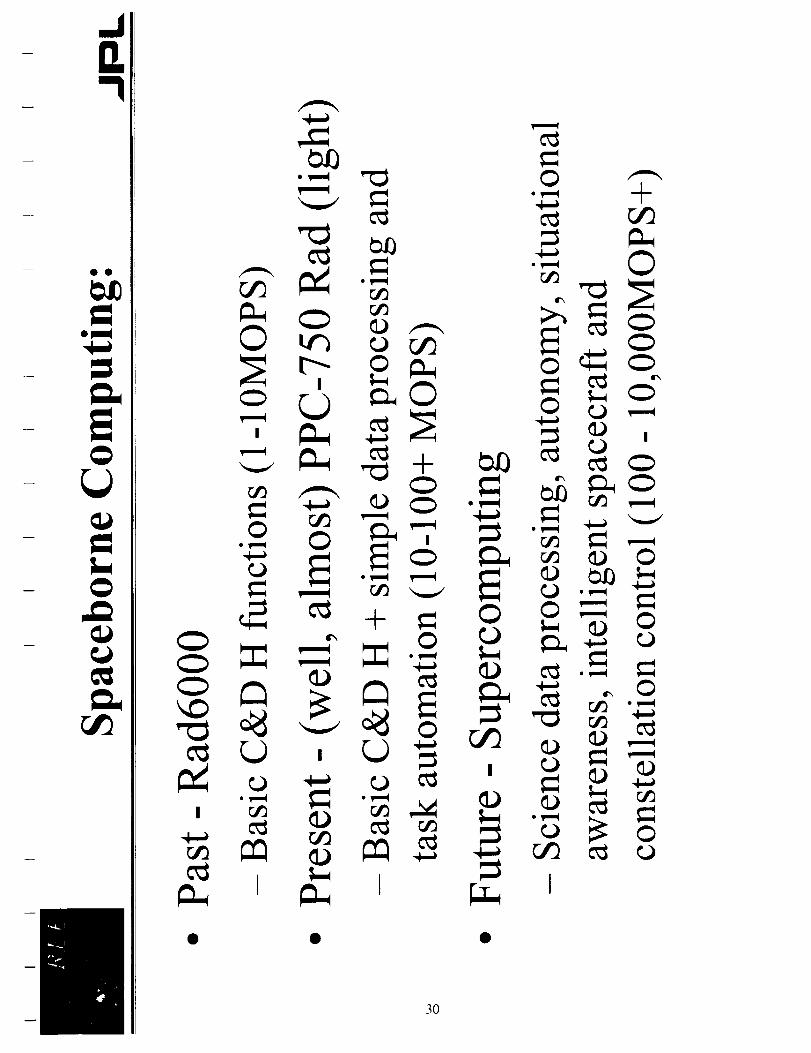
000
I
+©
• _ ° _..,,=I
3O
©°_ +
cf_
©
© 0f_
_J_
_j_
0 @ ---
.,_o _ o

_0
r,_
e_
""_ 0
0
,..0 '
.,_ ¢)
¢)
0r._r._
° I,'-_
°_
0
¢,..)
0
,.o0_,_
;>
©0 _0 _ 0
31
o_,_
O
©0_
,_o
;> 0
o O'-a
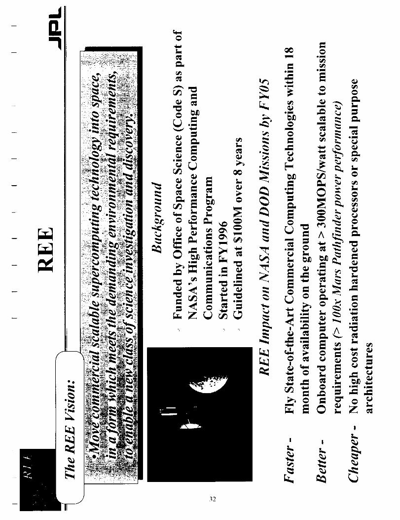
!
32

m°_
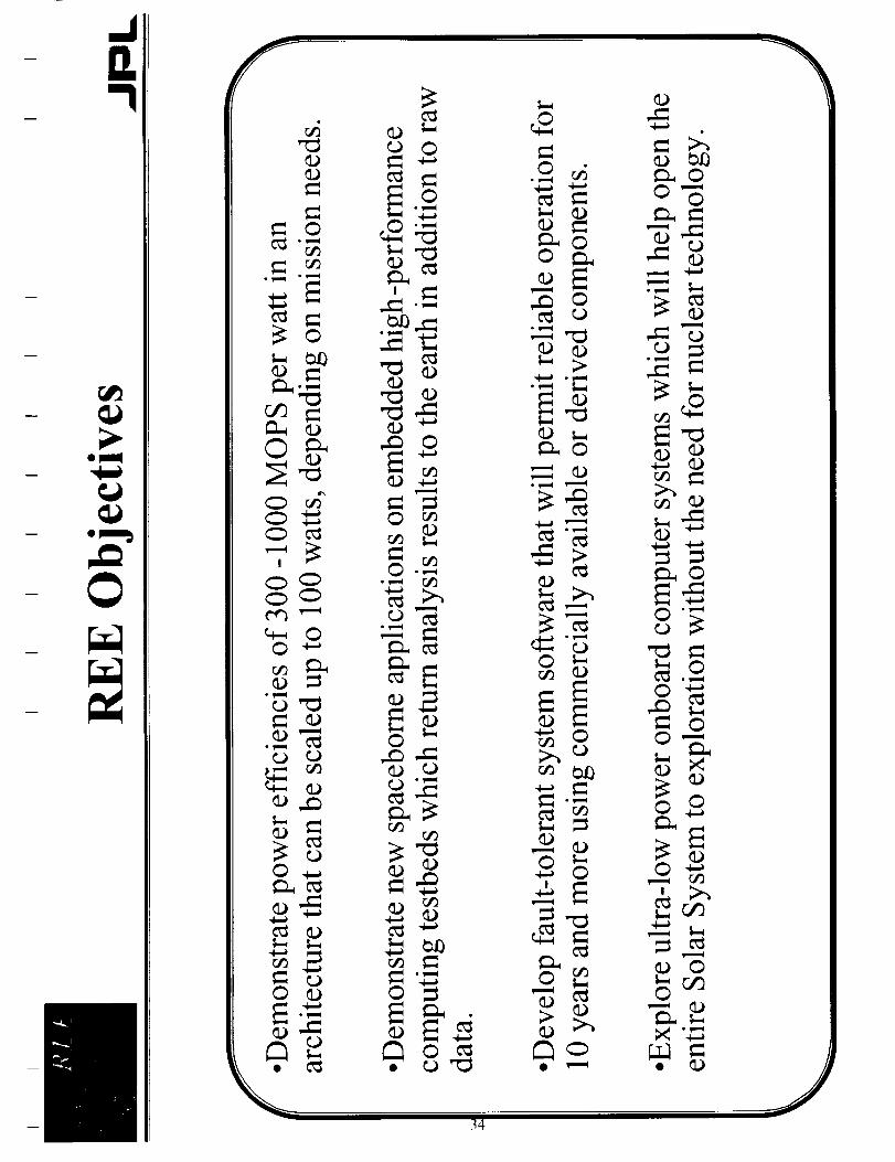
n
34


c_
c_
°_,,_
•_ o__
1.-0
0
0
_ C_
_s
L.m
36
0 0 0 0


opiq
©,,I--)
b0
©
° v.,-,I
0
.v.mq
I • •
,v,i-.q
• 'v,_l
- <= ,,,-,
.vm(©
00
• ,,,,,,
_ _-n _ ,-
I • _,--,I
i (L_ I
I I I I
38
=
0
0
C_
C_fx

n
o_
r_
39
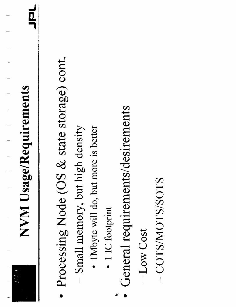
41
h
0
0
0
<
c'-I
[--.
i
42

i
0
0
0
43

0
*llqr_
mm
ol,ml
o _
*till
cn _
ew_
C_I •II II o_
u__
t-
_ °"_
.- = © > _
8_C/)
LL
_6
8
8-=_
o
=1-4
c_
_L
t_
_L_
0
c_
(L)
Z
0 0 _

o_m
olU
n_
E
0
°_
g.
°,.._
0
0
X
I
0
m
0
°_
_dn_
<_o
0
.o
n_
o
o
-o
.o
o
F-
0
0
0
n_
0
0
0
0
.0
_9
b0
E
E
0
E
E°_
0°_
0
0
0
"0
_0
°_
0
.ID
t_
0
E
n_
°_
.o < _,
_ d
E _
o _ _:*-.' 0
m _- b
_ .--.
X _
0 0 d m _.
-N _
m e, .-- "_
E E _
-- _oo
E _= oo
0
45
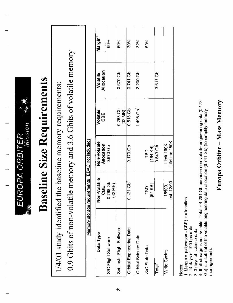
.=,
0
46

imm
i
II •
_J9
°v--_
I11
011
47

m
> E E E
= A_ -- Z_ Z_ Z_
>- >- Z Z Z Z Z Z
caI° ,,,,,,_
m
>
oJ_ C-I
I
0
F"
' o _ <
48
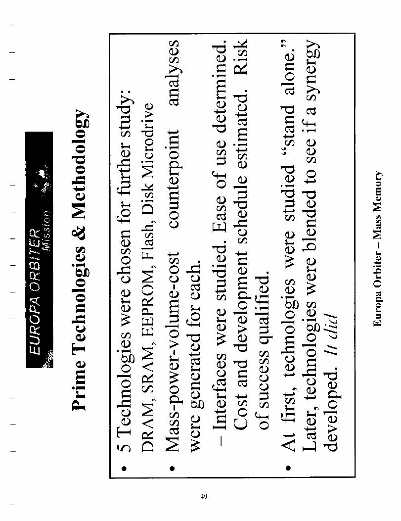
._L
49

• • • •
5O

r_
Imq
ojaq
I_u
mJml
51

r_
m
+
r_
<
r,.)
oo!IS aolaOAUOO
oo!IS
aolndtuoo lq_!IH
oo!IS INVBO
oo!IS HSV'-Id
r_
I
t-
52

0 ©
© © o,I
I
0
b.O
,_,ul
_0
0
-..x-
¢)
r._©
×
ot_

m
im
4-P
i
0
<
"dJ--,PI
r I|
_mPI
_mm_l
dmmql
_bmgl
_am_ I
_...,
i *
ina
_Z
o rm __ < _
= N a,
"_ _'J
I3_ I
@
54

rJ_
_o_
°_,mq
_ 0
_ 0©
©
< _0
_ .,_
_ Er_
_ b
I
oi
t,1
55

=
E

SESSION #2: Environment, Reliability &CharacterizationWednesday, November 7,2001
1:40 AM--4:20 PM
Chair: A. Johnston, JPL
1:40 PM
2:00 PM
2:20 PM
2:40 PM
3:00 PM
3:20 PM
3:40 PM
4:00 PM
Space Radiation Effects in Advanced Flash Memories; A. Johnston, JPL
Reliability and Radiation Characterization of an SOI EEPROM/FIash Memory
Cell; H. Peterson, C. Tabbert, F. Wright, H. Anthony, R. Reedy, and J. Cable,
Peregrine Semiconductor Corp.
Evaluation of Data Retention Characteristics for Ferroelectric Random Access
Memories; A. Sharma andA. Teverovsk3', Goddard Space Flight Center (NASA),
BREAK
Radiation Response of Emerging FeRAM Technology; D. Nguyen and L. Scheick,JPL
Characterization of Scaled SONOS NVSM Devices for Space and Military
Applications; S. Wrazien, J. Faul, Y Zhao, and M. White, Lehigh University,
D. Adams, Northrop Grumman Corporation, J. Murray, Sandia NationalLaboratories
Overview of Non-Volatile Testing and Screening Methods; F. lrom, JPL
An FPGA-Based Test-bed for Reliability and Endurance Characterization of Non-
Volatile Memory; V. Rao and J. Patel, University of Illinois, J. Patel and
J. Namkung, JPL
57

Space Radiation
l:j:'.:'.x
Effects in Advanced Flash MemoriestA 11. Johnston
Jet Propulsion Laboratory.California Instmtte of Yechnolo_
Pasadena, Cahfornia, USA
I, INTRODUCTION
Memory storage requirements in space systems
have steadily increased, much like storagerequirements in terrestrial systems. Large arrays of
dynamic memories (DRAMs) have been used insolid-state recorders, relying on a combination of
shielding and error-detection-and correction (EDAC)to overcome the extreme sensitivity of DRAMs to
space radiation. For example, a 2-Gbit memory(with 4-Mb DRAMs) used on the Clementine
mission functioned perfectly during its moon
mapping mission, in spite of an average of 71memory bit flips per day from heavy ions.
Although EDAC worked well with older types of
memory circuits, newer DRAMs use extremelycomplex internal architectures which has made it
increasingly difficult to implement EDAC Somenewer DRAMs have also exhibited catastrophic
latchup.
Flash memories are an intriguing alternative toDRAMs because of their nonvolatile storage and
extremely high storage density, particularly for
applications where writing is done relativelyinfrequently. This paper discusses radiation effects
in advanced flash memories, including generalobservations on scaling and architecture as well as
the specific experience obtained at the Jet
Propulsion Laboratory in evaluating high-densityflash memories for use on the NASA mission to
Europa, one of Jupiter's moons. This particular
mission must pass through the Jovian radiation belts,which imposes a very demanding radiation
requirement
The natural space radiation environment can
affect flash memories in four basic ways:
( I ) Macroscopic ionization damage from theinteraction of many electrons and protons,
producing a buildup of charge in gate andisolation oxides;
"l'The research m thts paper was carried out at the JetPropulsion Laboratory., Cahfomia Institute of Technology,under contract with the National Aeronautics and SpaceAdministration, Code AE, under the NASA ElectronicParts and Packaging Program (NEPP)
(2) Transient effects from the interaction of a
single galactic cosmic ray or high-energy
proton, causing upsets in the state machine,buffer or other digital regions of the flashmemory (this is analogous to upset effects from
alpha particles, but the particles in space
produce far more intense track densities);
(3) Microscopic tontzatton damage from the charge
produced by a single cosmic-ray heavy-ion in
the gate region; and
(4) Microscopic catastrophtc damage from highenergy protons or galactic cosmic ray particles
which can permanently increase the leakagecurrent of the floating gate
The first two mechanisms have been observed in
older flash memory technologies [1-3], as well as in
conventional memories and CMOS integratedcircuits. Evidence for the last two mechanisms has
been seen in evaluations of other memory'
technologies (particularly DRAMs), but they havenot been examined in detail for flash memories
II. FI,ASH TECHNOI.OGY EVOI.UTION
Flash memory applications can be divided into
two basic categories: code storage, which requiresfast, random access to all memory locations; andfile
storage, which mainly requires access to sequentialdata. Code storage flash memories usually use NORarchitecture, with independent read access for each
internal storage location. The cell size of aconventional NOR flash cell with LOCOS isolation
is _ 10-11 F 2, where F is the feature size of the
technology. Modern NOR flash devices use multi-
level storage (storing 3 different levels within each
cell and providing 2 binary bits) in order to improvethe effective storage density. This decreases the
effective cell size to approximately 6F 2, taking intoaccount the requirement for additional circuitry.
Multi-level storage reduces the margin between thethreshold voltage of the various levels in the floating
gate, and also requires a more sophisticated readouttechnology that can recognize the different charge
levels within the floating gates
58

FilestorageflashmemoriesuseNANDarchitecture,whichstacksncellstogethertoformaNANDlogicarraythatcanonly'beaccessedsequentiallySixteenor32cellsaretypicallyused,alongwithtwocontroltransistorsI4]. ThebasicNANDcelloccupiesonlyabout50%oftheareaof acorrespondingNORcell(withoutconsideringmulti-levelstorage)becausetheNANDcelldoesnotrequireseparateaccesstothesourceanddrainregionsof individualtransistorsin theNANDmemo_'stack.
Scalinginbothtechnologiesislimitedbytherequirementfor relativelyhighvoltagesforeraseandwritefunctions(12-20V). Aninternalchargepumpisnearlyalwaysusedto providethosevoltages.Specialtransistorswiththickergateoxidesarerequiredwithinthechargepumpaswellasin thecontrollogicforwritinganderasing.
NORflashmemorieshavebeenproducedwithmulti-levelstoragesince1998.Currently64-Mbdevicesareavailable,fabricatedwitha0.25_tmprocess,andhigherdensitydevicesareindevelopmentusingaprocesswithafeaturesizeofO18_tm[51.
NANDflashmemorytrendsareshowninFigure1,adaptedfromCoi,etal. [6]. There are two"'steps" in cell size trends that have reduced the cellsize. The first is due to shallow trench isolation in
1998; the second is due to the anticipated use of
multi-level cell technologies by mid-2001. NOR cellsizes are shown for comparison. Multi-level cell
technology was introduced in the NOR technologyin 1999. Dashed lines in the figure show
anticipated trends during the next year.
10
0_
o01
001
L r+"+'°=uJ 0"',, Multi-level
_',, , storage
N
Trench'_ch_ -_isolation
M ulti-level //
storage /
(projected)
I I I I1993 1995 1997 1999 2001
Time of Introduction
I2003 2005
Figure 1 NAND flash memory evolution The effective cell
size decreases by a factor of four when multi-level cell structures
are introduced NOR flash trends are shown for general
comparison
II] GLOBAL IONIZATION DAMA(iE
A. Basic Issues
Ionization from high-energy electrons andprotons in space produces electron-hole pairs within
gate and isolation oxides of MOS devices. Some ofthe excess chargc is trapped at the interfacc region,
changing the threshold voltage of the transistor. Forbasic MOS transistors the shift i11threshold voltage
scales with the square of the oxide thickness 171,
which has generally reduced the importance of total
dose damage in highly scaled devices
Although this same scaling scenario applies toflash memories, the internal transistors used for the
charge pump and erase/write control have muchthicker oxides because of the requirement for high
voltage This causes flash devices to be
considerably more sensitive to total dose damage
compared to other UI,SI technologies. It alsoimplies that write and erase functions will be the
first parameters to fail from total dose.
Figure 2 shows the results of probemeasurements of the internal charge pump for a 128-Mb NAND flash device The charge pump voltage
starts to degrade at about 6 krad(Si), and falls
rapidly at higher levels. At about 8 krad(Si) thedevice can no longer be erased. The shaded region
in the figure shows the range of failure levels fordifferent units from the same group of devices
14
12 [
10>g 8
>
_ 6
4
2
0
0
I I I I I I I 1
q
Measurements made on \
unlidded unit with special probe
\Fa#ed to erase "---'--"_-_11
Figure 2
7Samsung 128 MbFlash memory ] Range of feOure
levels for other _ ,4
unffs in ERASEor WRI TE mode
I I I I I I l I I
1 2 3 4 5 6 7 8 9 10
Total Dose [krads (Si)]
Degradation of the internal charge pump of a 128-Mb
NAND flash memory after irradiation wath garnma rays
The gate oxide thickness of high-voltage
transistors in this device is nominally' 200 A. At 8krad(Si), the shift in threshold voltage is about 70
mV, assuming 50% hole trapping
Flash memories will work at much higherradiation levels in the read mode. Figure 3 showstest results for an older NOR flash device that
compares functional operation for biased andunbiased devices (charge trapping is reduced when
no electric field is applied during exposure). When
59

the device is biased, field oxide inversion causes ahighly nonlinear increase in power supply current atabout 20 krad(Si)
0.8 , , , , r
Device Evaluated in "READ" Mode
_, ~1000 Read
0.6 I] Biased errors
I I irradiation ] _
II (static) I 11 to 13 /
_ o.4
0.2 | I Unbiased Il I ..... I _ One cell flipped
_ ' Irraa7 from0,o/"
........................................ £,_);c-t_m'ff.....
0 20 40 60 80 100 120 140
Total Dose [krad(Si)]
Figure 3 Effect of ionizing radiation on read mode operation of
a 16-Mb NOR flash memory The large increase in power
supply current at low total dose levels ts due to inversion of the[,OCOS field oxide structure
French isolation is used in more advanced flash
devices. Similar isolation leakage effects can occurin trench isolation structures. Processing detailsplay a large role in determining their sensitivity toradiation damage
IV. SINGLE-EVENT UPSET EFFECTS
d. Bamc Issues
Single-event upset sensitivity of flash memoriesis highly dependent upon the operating mode. If anion strike causes the internal state machine to bealtered, then the device will no longer workproperly This type of functional error is verydifficult to categorize because of the limitedinformation on the state machine that can be inferred
from external pins. Read, write and erase functionscan all be affected. In addition to the state machine,errors can also be introduced into buffers or other
active internal memory regions.
Although many different operating conditionscan be used for radiation testing, most tests are donewith the device in the read mode after a specificpattern is loaded (this assumes that write operationsare done infrequently, and that the probability of anion strike hitting a sensitive node during write orerase operations is small). After the device isexposed to a flux of ions, the memory contents areread out to see if the data has been altered or if the
device will still operate without being shut down andreinitialized
B, Repre.s'entatlve Text Results (Static Ah_de)
Tests on 16-Mb NAND flash technology with thedevice in a static mode during irradiation are shownin Figure 4. The ion used for these tests has anionization track density that is slightly above the"iron threshold" in the distribution of galacticcosmic rays, and thus is a reasonable measure of thedevice sensitivity to galactic cosmic ray effects. Thesame fluence ( 106 ions/era2) was used for each ofthe four test runs
Two points can be made concerning these data.First, functional operation was only affected duringtwo of the four test runs. When functional errors
occurred, they could either affect readout of thememory or other internal operation of the device inthe read mode (such as page-mode errors).ttowever, because the results are inconsistent fromrun to run, it is not possible to get the samestatistical precision about error rates compared withtests that show less ambiguous results.
Second, during the test run there were abruptincreases and decreases in the power supply currentThe current changes are likely due to upsets incontrol logic which cause conflicts in bidirectionallogic. The presence of the current steps indicate thatmany internal regions are affected However, upsetsin regions of the device that affect write or erasefunctions will not be detected by post-irradiationtests in the read mode.
E20
if?
"_"_ Run 1
30- I Mer'loryI P_rlors
_rffL -o
,,e-_ Run2_T _Run3 ---_, .,_--- Run4_
LET = 37 MeV-cm2/mgFluence = 106 ions/cm 2 per run
Time
Figure 4 Steps m power supply current during a heavy ion test
of a 16-Mb flash memory
Fortunately the cross section for upsets in thestate machine is relatively small compared to thetotal device area. The lower curve in Figure 5 showsthe upset cross section for a 16-Mb flash memory,dominated by upsets in the controller. Because ofthe small cross section, the error rate in space isrelatively low, corresponding to one error in timeperiods of several days to weeks (depending on theparticular orbit and other application details). The
6(1
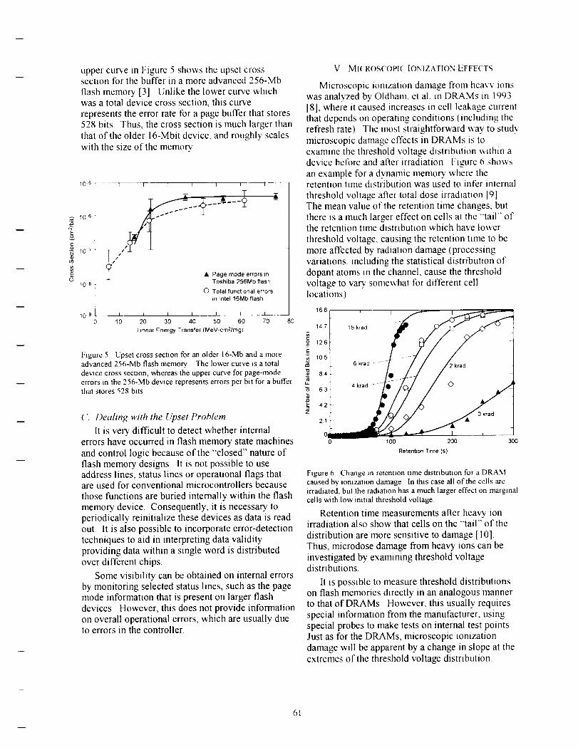
upper curve in Figure 5 shows the upset crosssection for the buffer in a more advanced 256-Mb
flash memory [3] Unlike the lower curve whichwas a total device cross section, this curve
represents the error rate for a page buffer that stores528 bits. Thus, the cross section is much larger than
that of the older 16-Mbit device, and roughly scales
with the size of the memory
10 5
10 6
_ 10_
......... 1
t0-8
10 9 10
I ; i I I i
_ T
//
/s
• Page mode errors mToshiba 256Mb flash
C) Total functional errors
in lntel 16Mb flash
1 I I I I I10 20 30 40 50 60 70 80
Linear Energy Transfer (MeV-cm2/mg)
Figure 5 Upset cross section for an older 16-Mb and a more
advanced 256-Mb flash memory The lower curve is a total
device cross section, whereas the upper curve for page-mode
errors m the 256-Mb device represents errors per bit for a buffer
that stores 528 bits
('. l)eahng with the Upset Problem
It is very difficult to detect whether internalerrors have occurred in flash memory state machines
and control logic because of the "closed" nature offlash memory designs. It is not possible to useaddress lines, status lines or operational flags thatare used for conventional microcontrollers because
those functions are buried internally within the flash
memory device. Consequently, it is necessary to
periodically reinitialize these devices as data is readout. It is also possible to incorporate error-detection
techniques to aid in interpreting data validityproviding data within a single word is distributed
over different chips.
Some visibility can be obtained on internal errorsby monitoring selected status lines, such as the pagemode information that is present on larger flash
devices. However, this does not provide informationon overall operational errors, which are usually dueto errors in the controller.
V MICROSCOPIC [ON1ZATION EFFE('TS
Microscopic ionization damage from heavv ions
was analyzed bv Oldham, et al. in DRAMs in L993[8], where it caused increases in cell leakage current
that depends on operating conditions (including therefresh rate) The most straightforward way to study
microscopic damage effects in DRAMs is toexamine the threshold voltage distribution within a
device before and after irradiation Figure 6 shows
an example for a dynamic memoo' where theretention time distribution was used to infer internal
threshold voltage after total dose irradiation [9]The mean value of the retention time changes, but
there is a much larger effect on cells at the -tail'" ofthe retention time distribution which have lower
threshold voltage, causing the retention time to bc
more affected by radiation damage (processing
variations_ including the statistical distribution ofdopant atoms in the channel, cause the threshold
voltage to vary somewhat for different celllocations)
168
147
126
105
84
63
42
21
00
n=,
E=z
6krad /0 (_/ /2krad '
/'A/
100 200 300
Retention Time (s)
Figure 6 Change m retennon time distribution for a DRAM
caused by iomzanon damage In this case all of the cells are
irradiated, but the radmnon has a much larger effect on marginal
cells vclth low inmal threshold voltage
Retention time measurements after heavy, ionirradiation also show that cells on the "tail" of the
distribution are more sensitive to damage [I 0]
Thus, microdose damage from heavy ions can be
investigated by examining threshold voltagedistributions.
It is possible to measure threshold distributionson flash memories directly in an analogous mannerto that of DRAMs. However, this usually requires
special information from the manufacturer, usingspecial probes to make tests on internal test points.
Just as for the DRAMs, microscopic ionizationdamage will be apparent by a change in slope at the
extremes of the threshold voltage distribution.
61

=io
,,QE
Z
Microscopic ionization damage has beenobserved in multi-level flash devices after irradiation
with heavy ions. "['he net effect was a shift of theinternal state of some of the internal memory cellsThis is shown schematically in Figure 7, where 18cells with the highest internal storage level wereshifted to the next level, 23 from the second highestto the third highest, and 2 from that level to theground level. This is caused by ionization(microdose) that changes the storage level of thecharge 'packet" within the floating gate. Althoughthis changes the stored intbrmation, it does not causea permanent change in the device; rewriting the cellcan be done to restore the information These typesof errors are expected to become more severe forfuture multi-level flash memories, particularly iflarger numbers of bits are stored within each cell,because the internal margin for changes in thresholdvoltage is reduced
100000
10000
1000
100
10
1
i i
2
2 3
i i
23 18
12 Ill
: o I
I, IL, :4 5
Cell Threshold Voltage (V)
%t!
I
°t
6
Figure 7 Change in higher-level storage locations m a multi-
flash memory after irradiation with heavy ions
VI. PERMANENT ERRORS CAUSED BY MICROSCOPIC
DAMAGE
l'ermanent changes in thin oxide can occur dueto the detailed interaction of the intense ionization
track from a single heavy ion with the gate region,which produces localized damage in the structure ofthe gate [10]. The earlier work was done with 4-MbDRAMs, and similar effects have been observed in16 and 64-Mb DRAMs. This effect has been studied
more recently in capacitor test structures [11], andcan cause the leakage current to increase by severalorders of magnitude. Figure 8 shows an example ofthis effect. Although the change in leakage currentis small, it can affect the ability of the floating gateto store charge over long time periods. This is apermanent effect, and may limit the ability to usevery advanced flash memories in space unless they
are refreshed periodically The magnitude of theleakage current depends on the thickness of the gateregion as well as the quality of the oxide.
102 --T 1 f r ?--Jt--f--
10 _ Hard '
Breakdown_" 10 °E
,;,',il//tlo-2 Au(82 . J i111 I-
I-,7, 10-3 ,..; :,,-,Soft Breakdown ,,¢_ • .' .'# I t /, I
10 .4 --.,_/ • .. • I l/" A -
..,.4.,,i.----"i='-_- -- ,_'." I ,P/I10-_, _.,r - _ =-"i,_lk-'ll lilt #1 -
"._" ll,"i . - ..l_lET- I 1I II10-6 ;:;;;;;_;;iill dl<ilt= "'= ...... _""1(60) IlJ,, 'x .
10 -7 _(375)-
10 8 _ , _ 10 1 2 3 4 5
Stress Voltage, Va_ (IVl)
Figure 8 Increase in leakage current of a thin oxide after
irradiation with heavy ions
Although high electric fields are required in orderto get large current changes (hard breakdown), softbreakdown can occur at very low electric fields andrequired only a single ion strike. It is possible todeal with this issue by rewriting the memoryperiodically (similar to refresh in a DRAM, but on amuch longer time scale), but this failure mode isclearly an important issue for applying advancedflash memories in space. It may become moreimportant for flash memories in the near futurebecause of the constant requirement to decrease cellsize and increase erase/write efficiency.
Other microscopic damage mechanisms may alsobe important for more highly scaled devices,including microscopic displacement damage fromprotons. More work is required in order todetermine how small cell geometries and moreelaborate memory' architectures are affected byspace radiation.
VII. CONCLUSIONS
Flash memories have unique design requirementsthat cause them to be more susceptible to radiationdamage compared to more conventionalmicroelectronic components. The high voltagerequired for the erase and write functions requirethat some of the internal transistors are designedwith thicker gate oxides and more lightly dopedchannel regions compared to conventional digitallogic transistors, making them far more susceptibleto radiation damage. The charge pumps that arerequired to generate the high voltage for erasing andwriting are usually the most sensitive circuit
62

functions, usually failing below 10 krad(Si) Someimprovement can be realized by operating the flashmemory devices without bias except during the timeperiods that they are required to operate, and thatmethod has been proposed for possibleimplementation of advanced flash memories on theJPL Europa mission.
Single-event upset effects are far more difficultto deal with The very complicated devicearchitecture used in advanced flash devices causes
their basic functionality to be affected by hea_ ionsand protons, and it is difficult to recognize andcategorize these types of upsets because of thelimited visibility about internal operating conditionsIn some cases the device clearly does not function atall, but in others the errors may be difficult to detect-- such as errors in buffers or page address registersFortunately the overall error rate for those types ofmalfunctions is relatively small, allowing systemmitigation with EDAC
Permanent errors are a far more difficult problemfor several reasons. First, tests of permanent errorsare difficult and costly to perform. Second, sometypes of errors may occur even for devices that arenot biased during the time that a heavy ion strikeoccurs. Error detection and correction may be aviable way to recognize this type of failuremechanism, but it is also necessary to understandhow and why the errors are generated within thedevice, as well as whether internal errors in thememory controller will affect their operation in
space
[7] N S Saks, M G Ancona and J A Modolo, 'Radlanon
[-ffects in MOS Capacitors with \'e_' Thin OxMes at gO K'
[EEE Trans Nucl Scl , 31(6) 124 _) (1084)
[8] T Oldham et al , _'Tolal Dose Fadures m Advanced
Electronics from Single Ions," ll!f-E Trans Nucl Sc_
40(6), 1820 (19c)3)
[91 L Z Schetck, S M Guerttn and G M S_aI't, "Analysis of
Radiation Effects on Individual DRAM Cells ' IEEE Trans
Nuc[ Sct , 47(6), 2534 (2000)
[10] G M Swift D J PadgettandA I1 Johnston, "A Nev,
Class of Single-l-vent Hard Errors," IEliE Trans Nucl Scl
41(6), 2043 (1994)
[ 11 ] J E Conley, el al , ""Heavy Ion Induced Soft Breakdov, n of
Thin Gate Oxides," presented at the 2001 IEEE Nuclear
and Space Ra&anon Effects Conference. Vancouver
Brmsh Columbia, July 16-20, 2001, accepted for
pubhcation in the [EEE Trans Nucl Sc_ December. 200l
REFERENCES
[I] H R Schwartz, D K Nichols and A H Johnston,_'Smgle-
Event Upset in Flash Memories," IEEE Trans Nucl Sci,
44(6), 2315 (1997)
[2] D N Nguyen, et al, "Radiation Effects in Advanced Flash
Memories," IEEE Trans Nucl Sci, 46(6), 1744 (1999)
[3] D R Roth, et al, "SEU and TID Testing of the Samsung
128 Mbit and the Toshiba 256 Mbit Flash Memory," 2000
IEEE Radiation Effects Data Workshop, p 96
[4] S Antome, "Advanced Flash Memory Technology and
Trends for File Storage Applications," 2000 IEDM
Technical Digest, p 763
[5] A Fazlo, "A Htgh-Density High-Performance 180 tam
Generatton ETOX Flash Memory Technology," L999
[EDM Technical Digest, p 267
[6] J-D Col, et al, "A 0 15 lam NAND Flash Technology w_th
0 1 I p.m 2 (,,ell Size for l-Gbit Flash Memory.," 2000 IEDM
Technical Digest, p 767
63

c_
// /
LII
Reliability and Radiation Characterization of an SOl EEPROM/FiashMemory Cell
i lank Peterson, Chuck Tabbert, Frank Wright, I lal Anthony', Ron Reedy, Jim Cable
Peregrine Semiconductor Corp, 6175 Nancy' Ridge Drive, San Diego, CA 92121
Abstract
This paper describes the on-going work,sponsored through the Defense ThreatReduction Agency (DTRA) SBIR program,at Peregrine Semiconductor Corp tocharacterize radiation and endurance
behavior of the Peregrine's patentedPlusCellr'_ a new nonvolatile memory cell
which utilizes a standard CMOS process on
Vi_ s +
: ,t3
_tt, ra[anch¢ iniechon/
l'loating gate j/ of holes
___
";apphirc
Silicon island _n._ gale
r . ._,ll i............. r?f,,,, _ecn_ln ,k
i ! pV [
i i
IN
i
Figure l PlusCell IM EEPROM basic cell
a silicon on insulator technology.
Introduction
The Peregrine's patented PlusCell r,_t shownin Figure ! is one of several technologies
Figure 3 Turning on the N-channel byavalanche injection of holes (Cross-section B)
currently under development which offer thepotential for radiation hardness, goodendurance and solid data retention The
PlusCell r,u using both hole and electron
injection (see Figures 2 and 3), has severalkey advantages, including elimination of anyover-erase mechanism, a dense cell,
availability of bi-directional read, andefficient block erase. The layout of the
1.21am PlusCell nt is shown in Figure 4.
Figure 2 Turning on P-channel transistor by
avalanche injection of electrons (Cross-section A)
Figure 4 1.2xl.2 lttm E 2 Cell for
DTRA Characterization
64
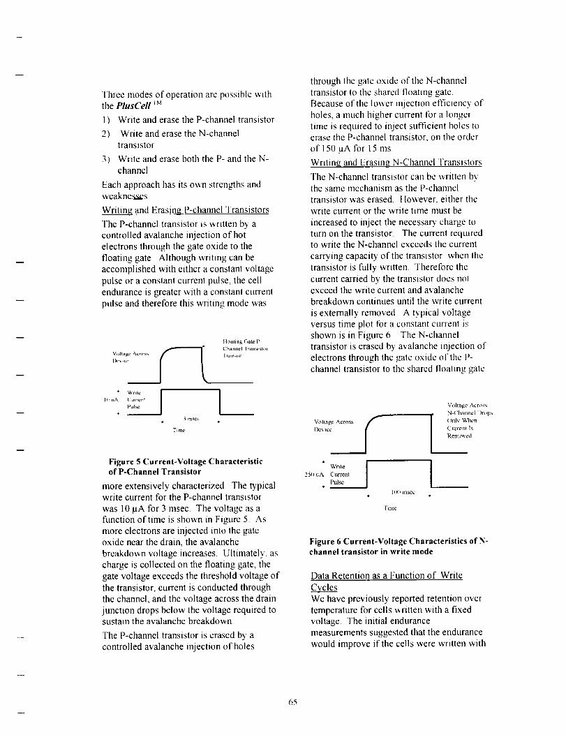
Three modes of operation arc possible withthe PlusCell _M
I) Write and erase the P-channel transistor
2) Write and erase the N-channel
transistor
3) Write and erase both the P- and the N-channel
Each approach has its own strengths andweaknesses.
Writing and Erasing P-channel Transistors
The P-channel transistor is written by a
controlled avalanche injection of hot
electrons through the gate oxide to the
floating gate. Although writing can be
accomplished with either a constant voltage
pulse or a constant current pulse, the cell
endurance is greater with a constant current
pulse and therefore this writing mode was
DeviccV°hagc,\cms_
• _'rilc J
IO uA Curren_
Pulsc
3 msec
Time
Floating Gate P-
Channel I ransislOl
I urn-on
LI
Figure 5 Current-Voltage Characteristicof P-Channel Transistor
more extensively characterized The typicalwrite current for the P-channel transistor
was 10 taA for 3 msec. The voltage as a
function of time is shown in Figure 5. As
more electrons are injected into the gateoxide near the drain, the avalanche
breakdown voltage increases. Ultimately, as
charge is collected on the floating gate, the
gate voltage exceeds the threshold voltage of
the transistor, current is conducted through
the channel, and the voltage across the drain
junction drops below the voltage required tosustain the avalanche breakdown.
The P-channel transistor is erased by a
controlled avalanche injection of holes
through the gate oxide of the N-channel
transistor to the shared floating gate
Because of the lower rejection efficiency of
holes, a much higher current for a longer
time is required to inject sufficient holes toerase the P-channel transistor, on the order
of 150 gA for 15 ms
Writing and Erasing N-Channel Transistors
The N-channel transistor can be written bythe same mechanism as the P-channel
transistor was erased. However, either the
write current or the write time must be
increased to inject the necessau charge to
turn on the transistor. The current requiredto write the N-channel exceeds the current
can3'ing capacity of the transistor when the
transistor is fully written Therefore the
current carried by the transistor does nolexceed the write current and avalanche
breakdown continues until the write current
is externally removed A typical voltage
versus time plot for a constant current is
shown is in Figure 6 The N-channel
transistor is erased by avalanche injection of
electrons through the gate oxide of the P-
channel transistor to thc shared floating gate
Voltagc Across
I )_'vic("
Write
25ql uA Current
Pulse,r
f
Voltage Across
N-Channel I)rops
( )nl', _tmn
Current Is
Removed
1(_) msccP
Time
Figure 6 Current-Voltage Characteristics of N-channel transistor in write mode
Data Retention as a Function of Write
_C__.vcles
we have previously reported retention over
temperature for cells written with a fixed
voltage. The initial endurance
measurements suggested that the endurance
would improve if the cells were written with
65
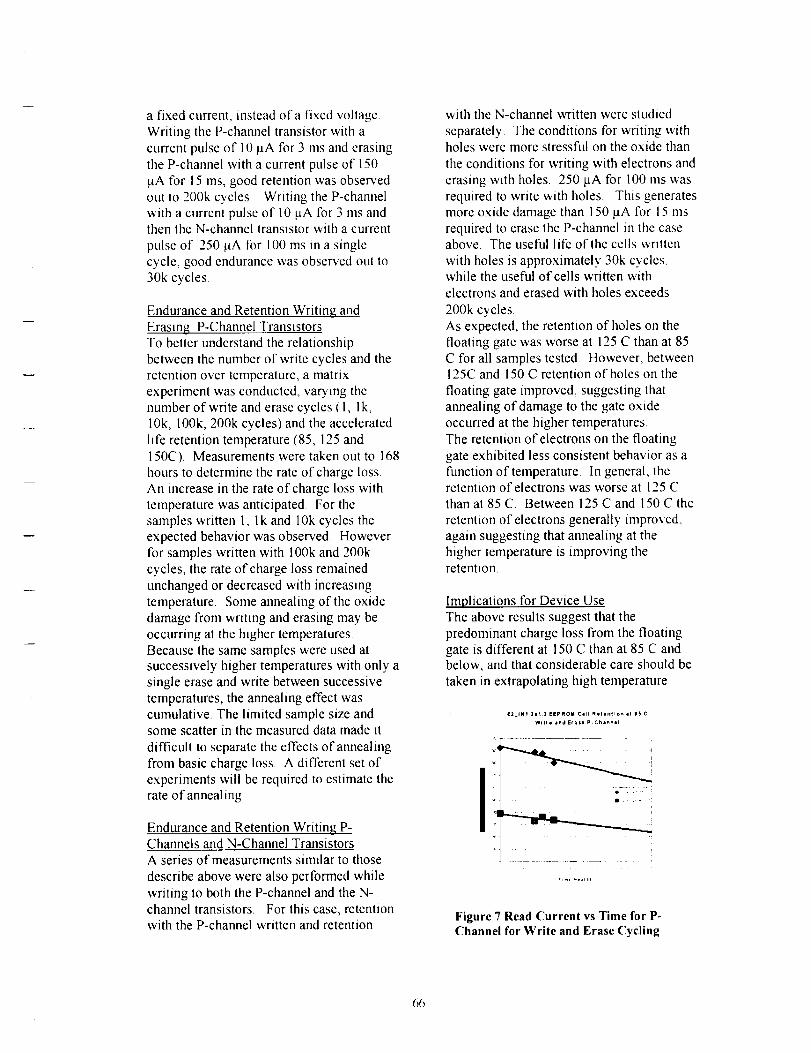
a fixed current, instead of a fixed voltage.
Writing the P-channel transistor with acurrent pulse of 10 p.A for 3 ms and erasingthe P-channel with a current pulse of 150
gA for 15 ms, good retention was observedout to 200k cycles. Writing the P-channelwith a current pulse of 10 pA for 3 ms andthen the N-channel transistor with a current
pulse of 250 gA for 100 ms in a singlecycle, good endurance was observed out to
30k cycles.
Endurance and Retention Writing and
Erasing P-Channel TransistorsTo better understand the relationship
between the number of write cycles and theretention over temperature, a matrixexperiment was conducted, varying thenumber of write and erase cycles (1, lk,10k, 100k, 200k cycles) and the accelerated
life retention temperature (85, 125 and150C) Measurements were taken out to 168hours to determine the rate of charge loss.An increase in the rate of charge loss withtemperature was anticipated. For thesamples written 1, Ik and 1Ok cycles the
expected behavior was observed. Howeverfor samples written with 100k and 200kcycles, the rate of charge loss remainedunchanged or decreased with increasingtemperature. Some annealing of the oxidedamage from writing and erasing may beoccurring at the higher temperatures.
Because the same samples were used atsuccessively higher temperatures with only a
single erase and write between successivetemperatures, the annealing effect wascumulative. The limited sample size andsome scatter in the measured data made it
difficult to separate the effects of annealing
from basic charge loss. A different set ofexperiments will be required to estimate therate of annealing
Endurance and Retention Writing P-Channels and N-Channel TransistorsA series of measurements similar to those
describe above were also performed whilewriting to both the P-channel and the N-channel transistors. For this case, retentionwith the P-channel written and retention
with the N-channel written were studied
separately. The conditions for writing withholes were more stressful on the oxide than
the conditions for writing with electrons anderasing with holes. 250 laA for 100 ms wasrequired to write with holes. This generatesmore oxide damage than 150 laA for 15 msrequired to erase the P-channel in the caseabove. The useful life of the cells written
with holes is approximately 30k cycles,while the useful of cells written with
electrons and erased with holes exceeds
200k cycles.As expected, the retention of holes on thefloating gate was worse at 125 C than at 85C for all samples tested, ttowever, between125C and 150 C retention of holes on the
floating gate improved, suggesting that
annealing of damage to the gate oxideoccurred at the higher temperatures.The retention of electrons on the floating
gate exhibited less consistent behavior as afunction of temperature. In general, theretention of electrons was worse at 125 Cthan at 85 C. Between 125 C and 150 C the
retention of electrons generally improved,again suggesting that annealing at thehigher temperature is improving theretention.
Implications for Device UseThe above results suggest that thepredominant charge loss from the floatinggate is different at 150 C than at 85 C andbelow, and that considerable care should be
taken in extrapolating high temperature
_q
E2_INt 111 / IEIEPROIII CiII Relen_lon at IS C
WrHI 8ha [riSl P-Channel
II <.. - -'
Figure 7 Read Current vs Time for P-Channel for Write and Erase Cycling
66

results back to normal operating
temperatures, particularly for devices which
have seen a large number of write and erase
cycles. In applications where the number of
write and erase cycles is large, writing with
electrons and erasing with holes will yield
superior results. The retention for cells with
100k and 200k cycles is shown in Figure 7
Radiation Hardness
The EEPROM cell was tested for radiation
hardness as a stand-alone element. The
retention as a function of x-ray radiation
dose is shown in Figures 8 and 9 in the two
modes of operation
Reading P-Channel Transistor
(After 10k C-_les )
0
v
-to
-15"Ot_
-20
-25
A"1" /"
Prerad Post 100k
Figure 8 Radiation response of EEPROMcell for a P-Channel read
Reading the P-channel transistor is similar in
operation to conventional EEPROM cells,i.e. the current from the P-channel transistor
25<
20
_ 5o
Reading N-Channel Transistor
(After 10kCy:le$)
"0"_
Prerad Post 100k
X-ray Radiation Exposure
Figure 9 Radiation response of EEPROM cellfor an N-channel read
is detected by a sense amp as a "'1""or a '0""
As can be seen in Figure 8, the current
difference between a ""1""and a "0"" is greatlyreduced after 100 krads. Tile N-channel
transistor can be read in a similar manner.
Note that at 100 krad the difference between
a "1"" and a "'0" has not collapsed as much
for the N-channel transistor (Figure 9) as for
the P-channel transistor (Figure 8).
The PlusCell IM can also be incorporated in
a latch using a shared gate for both the
EEPROM cell and an output inverter. By
writing with the P-channel transistor
(electron inJection) and the N-channel
transistor (hole injection), the inverter output
will switch between the power supply rails
The performance of this cell is shown in
Figure 10 for x-ray radiation doses up to 300krads
EEPROM Latch Output Voltage
(Vdd=3.0V)
_ 3¢ # # # # ¢ ¢ ¢ ¢ ¢ ¢ @ tA
o_
0 _0 200 300
X-Ray Radiation Exposure (kRads)
Figure 10 EEPROM latch output voltage as afunction of x-ray dose
Conclusions
The characterization data has shown that the
PiusCell 7;_tshould become a viable memory
cell for use in military and spaceapplications. The PiusCell 7_ will be the
basis for embedded EEPROM applications
by the Space & Defense community' along
with introductions of high-density EEPROM
devices Peregrine Semiconductor Corp. is
also using the PlusCell 7_ in its RF and
photonics products for both trimming andtuning.
67

_' I_
Evaluation of Data Retention Characteristics for
Ferroelectric Random Access Memories
(FRAMs).
Ashok K. Sharma/NASA. Greenbelt MD 20771
Ashok.k.Sharma. 1(a).._zsfc.n asa. _zov
Alexander Teverovsky/QSS Group, Inc./NASA, Greenbelt MD 20771
Alexgndel'.A.Teverovskv. l (a!_s fc.nasa._zov
Abstract. Data retention and fatigue characteristicsof 64 Kb PZT-based FRAM microcircuits
manufactured by Ramtron were examined over
temperature range from -85°C to _310 °C for ceramic
packaged parts and from -85°C to _175 °C for plastic
parts, during retention periods up to several thousand
hours. Intrinsic failures, which were caused by a
thermal degradation of the ferroelectric cells,
occurred in ceramic parts after tens or hundreds hours
of aging at temperatures above 200 °C. The
activation energy of the retention test failures was
1.05 eV and the extrapolated mean-time-to-failure
(MTTF) at room temperature was estimated to be
more than 280 years. Multiple write-read cycling (up
to 3x10⁷) during the fatigue testing of plastic and
ceramic parts did not result in any parametric or
functional failures. However, operational currents
linearly decreased with the logarithm of number of
cycles thus indicating fatigue process in PZT films.
Plastic parts, that had more recent date code as
compared to ceramic parts, appeared to be using die
with improved process technology and showed
significantly smaller changes in operational currentsand data access times.
TABLE OF CONTENTS
1.0
2.0
3.0
4.0
5.0
6.0
INTRODUCTION
EXPERIMENTAL DETAILS
DATA RETENTION TEST RESULTS
FATIGUE TESTING
CONCLUSIONS
ACKNOWLEGMENTS
1.0 INTRODUCTION
Low power consumption and high operation speed
make ferroelectric random access memory
microcircuits (FRAM) very attractive for space
applications, especially for long-duration missions.
The FRAMs have two orders of magnitude less write
access time and require three orders of magnitude
less energy per bit write compared to conventional
nonvolatile memory devices (EEPROMs and/or Flash
Memory) Driven by variety of commercial
applications, the density of ferroelectric memories
has improved dramatically over the last years. The
first, 4 kb, commercially available FRAMs were
manufactured by Ramtron less than ten years ago and
now memory densities of 1 Gb based on 0.18 um
technology appear to be technically feasible [1 ].
Ferroelectric memories have potentially high
radiation tolerance. The ferroelectric capacitors,
which are used as memory cells, had been shown to
be tolerant to total ionization dose grater than 1
Mrad(Si) without loss of polarization [2], [3]. In
many cases the radiation tolerance of the FRAM
microcircuits is limited by CMOS circuit elements.
By this reason the radiation response of commercial
devices with and without ferroelectric films was
similar for both parts [4].
One of the major reliability issues for all nonvolatile
memory devices, FRAM including, is data retention,
which is defined as the ability of a microcircuit to
maintain stored data between the time of writing and
subsequent reading of the stored information.
Temperature significantly accelerates retention
failures due to thermal depolarization of the poled
state in the ferroelectric material and is conTnonly
used to accelerate this failure mechanism.
Experiments on low density Ramtron FRAM
microcircuits have demonstrated the failure rate of
less than 60 fits with a 60% confidence level for 10-
year data storage at room temperature [5]. However,
retention characteristics depend on multiple
manufacturing and design factors and remain a major
reliability concern for new generations of FRAM
microcircuits.
68

Anotherdegradationmechanism,whichisknowntoaffect reliability of ferroelectricmemorymicrocircuitsis fatigue. Fatiguein ferroelectricmaterialsis a decreaseof switchablepolarizationwith increasednumberof switchingcyclesorpolarizationreversals.Thisdegradationprocessisrelatedto the electrodeinterfacialareasof thememorycellsandcanbesignificantlydecreasedbyusingappropriateelectrodematerials,for exampleRuO2/PZTstructures,insteadof Pt/PZTstructures[6]. "['he electric-field-assisted migration of charged
species (most likely oxygen vacancies) within
ferroelectric materials may be also responsible for the
degradation/fatigue behavior [ 7 ], [8 ].
[n addition to retention and fatigue failures, other
failure modes and mechanisms, such as aging,
imprint and reducing environment degradation are
known to be specific to ferroelectric memory cells in
microcircuits.
Aging is defined as a mechanism which causes
signal loss during a retention period which does not
recover after a rewrite and immediate read. This
differentiates it from the retention failures, where a
signal recovers aftra rewrite and immediate read
Aging is considered as a gradual stabilization of the
domain structure due to which the ferroelectric
becomes less responsive to applied fields [9], [10].
Imprint is a phenomenon specific to the ferroelectric
materials. Oace a capacitor spent significant time in
one polarity, it is reluctant to switch polarities [11].This effect is due to accumulation with time of
charges in the ferroelectric cell, which compensates
the created polarization.
Annealing of Pt/PZT system in a hydrogen-
containing ambient (e.g,, forming gas) might cause
severe degradation of PZT thin film [12]. Hydrogen
that reaches the platinum-PZT interface is a strong
enough reducing agent, with Pt as a catalyst, to take
oxygen from the lead lattice of the PZT. This results
in forming a water molecule, which reduces the
adhesion between the PZT and platinum and
degrades the signal from the ferroelectric cell. It was
shown [131 that the hydrogen evolved from plastic
packaging during molding and post mold rare can
affect data retention reliability of FRAMs. Another
mechanism of polarization suppression in PZT films
is related to high temperature reducing treatments in
dry nitrogen at 400 °C [14]. This treatment creates
oxygen vacancies which might lock domains. The
trapped charges are believed to inhibit the domain
motion and cause failures of memory cells.
Ferroelectric memory is a relatively new, emerging
technology, which requires in-deep understanding of
the related reliability issues and extensive testing at
extreme conditions beli_re it can be approved for
space applications, fhe objective of this work was to
evaluate reliability of commercial 64 kb FRAMs.
available from Ramtron. over a wide temperature
interval with a focus on data retention characteristics
2.0 EXPERIMENTAl. DETAIl .S
2.1 Parts Description.
Fifty [-'RAM microcircuits in ceramic 28-DIP
packages (FM1608S-250CC) and filly microcircuits
in 28-DIP plastic packages (FM 1608-P)
manufactured by Ramtron were used for thisevaluation. The FM1608 i; a 64 Kbit. nonvolatile
memory; organized as 8,192 x 8 bits The complete
address of 13-bits specifies each of the 8, t92 bytes
uniquely. The microcircuit is based on two-
transistors, two-capacitors memory cells 12T2C).
which had been proved to provide most robust data
retention reliability [1 ]
2.2 Test Description.
A total of 100 parts, 50 each of ceramic 28-pro DIPs
and plastic 28-pin DIPs were divided into various
groups and subjected to high temperature storage
aging tests at 150 °C, 175 °C, 200 °C*, 225 X'*, 250
°C*, and 275 _C* (* ceramic packages only) for up to
several thousand hours cumulative The interim and
final electrical measurements (EM) for each group
were performed at room temperature. Low
temperature testing was performed on a lot of parts at
85°C Temperature cycling was performed
between 65°C and +150°C for 425 cycles with
interim and final EM In addition, fatigue testing by
extensive read-write cycling, and total dose ionizing
radiation testing were performed on some lots of
parts
2.3. Electrical measurements.
Electrical measurements were performed using
HP82000 digital tester and included parametric andfunctional measurements. The parametric
measurements incorporated the measurements of
input and output voltages and leakage currents (VOL,
VOH, IlL, IIH, ILO_L, ILO_H), stand-by and active
power supply currents (ICCSB_cmos, ICCSB_ttl,
ICCOP) and chip enable access time, tCE. During
the functional testing, six data patterns ("scan 1",
"'scan 0", "'check error board" and three pseudo-
random patterns) were consequently written and then
read in each test sample. The functional test
frequency was I MHz.
To evaluate retention characteristics, each sample
was subjected to parametric measurements and then
functionally tested with the pseudo-random pattern 1
69

(PRP1). Electrical measurements after the parts had
been stressed for a specified period of time (retention
period) at specified environmental conditions, began
with reading the PRPI and followed by the
parametric measurements. A number of failed
vectors obtained after the first PRP1 reading was
used to estimate proportion of the failed cells
All parts passed radiography and PIND testing and
then were preconditioned by 10,000 write-read
cycles No failures during preconditioning and/or
initial electrical measurements were observed.
3.0 DATA RETENTION TES]
RESUI,TS
l'he li)llowing sections summarize retennon test
results for high temperature aging, low temperature
exposure testing, total dose radiation testing, and
temperature cycling.
3.1 High Temperature Step-Stress Tes!
']'he lead zirconate titanate (PZT) remains
ferroelectric up to +350 °C (Curie temperature for
PZT is about 670 K) tlov_ever, thermal bakes at
temperatures below the Curie point can degrade
ferroe[ectric capacitors as a result of the relaxation
phenomenon and aging [13]. Besides, it was not
clear whether the CMOS circuits in the parts and the
used packaging system can withstand temperatures
above 150 °C
To estimate the temperature range, which causes high
rate of the retention failures, and to assure that the
ceramic parts can withstand high temperature bakes
without catastrophic failures, a high temperature step-
stress was performed. Three ceramic parts were
subjected to one-hour temperature bake in the range
of150 °C to 310 °C. Test results are summarized in
Table 1. Two vectors failed in one of the parts after
175 °C, but then this part passed 200 °C test and no
failures were observed up to the step-stress of 285 °C
with only a few vectors failed at l0 °C. These
results suggest a good thermal tolerance of the parts
and indicate the possibility of performing high
temperature storage testing.
3.2 High Temperature Aging
Initial electrical testing (at 25°C) was performed on
two lots of 5 ceramic and 5 plastic parts, with
interim/final EM at 168, 273, 1000, and 5124 hours.
All ceramic parts passed all EM. Two out of five
plastic parts failed some test vectors on post-273
hours EM, but then passed post-1000 and 5124 hourstests. Test results are summarized in Table 2
Table I Data Retention Results (failed vectors) [\_r
the Step-Stress Test.
T,'CI 77I SN7.I SN150 0 0 0
175 0 0 2
200 0 0 0
225 0 0 0
240 0 0 0
255 0 0 0
270 0 0 0
285 0 0 1
300 1 0 1
310 1 2 1
79
Table 2 Data Retention Iest._ al Room Temperature
(25°C)
RT, Ceramic Parts
Hrs Failed Failed
parts vectors
168 0/5 0
273 0/5 0
1000 0/5 0
5124 0/5 0
Plastic Parts
Failed Failed
parts vectors
1/5 4
2/5 3
0/5 0
0/5 0
High temperature aging at 150 °(' was performed on
two lots of 5 ceramic and 5 plastic parts, with interim
and final EM up to 6330 cumulative hours. The same
vector in one out of five ceramic parts failed at
retention time (RT) of more thenl5 hours. A
significant increase in failed vectors was observed in
ceramic parts at RT > 1000 hours. Intermittent
failures were observed for the plastic parts during
some interim EM, which cleared up during the
following EM, but then again reappeared. Test
results are summarized in Table 3.
Table 3. Data Retention Tests at 150 °C.
Total iRT, Ceramic Parts Plastic Parts
time, hrs Failed Failed Failed Failed
hrs parts vectors parts vectors
3 3 0/5 0 1/5 1
18 15 1/5 1" 3/5 9
98 80 1/5 1" 0/5 0
268 170 1/5 1" 2/5 7
698 430 1/5 l* 2/5 3
1698 1000 1/5 5* 3/5 5
6330 4632 _5 23* 2/5 5
same vectors
70
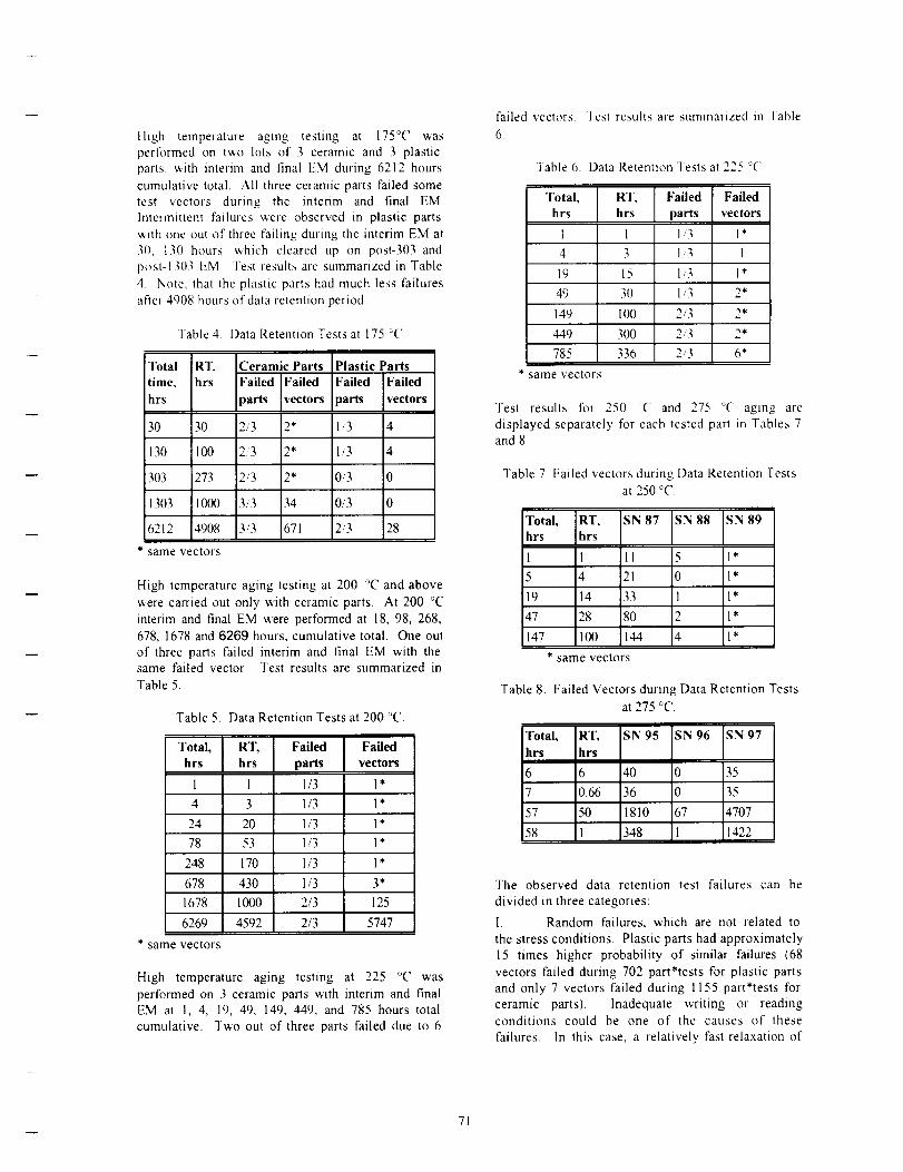
[ligh temperature aging testing at 175°C was
performed on t_o lots of 3 ceramic and 3 plastic
parts, with interim and final EM during 6212 hours
cumulative total. All three ceramic parts failed some
test vectors during the interim and final EM
Intermittent failures were observed in plastic parts
,,'_ith one out of threc failing during the interim EM at
30, 130 hours, which cleared up on post-303 and
post-1303 iiM Test results are summarized in Table
4. Note, thai the plastic parts had much less failures
afte) 4908 hours of data retention period.
Table 4. Data Retention Tests at 175 '>('
Total
time,
hrs
30
130
303
1303
6212
RT, Ceramic Parts Plastic Parts
hrs Failed Failed Failed Failed
parts vectors parts vectors
30 2/3 2* 1/3 4
I00 2/3 2* I/3 4
273 2/3 2* 0/3 0
1000 3/3 34 0/3 0
4908 3/3 671 2/3 28
* same vectors
High temperature aging testing at 200 °C and above
were carried out only with ceramic parts. At 200 °C
interim and final EM were performed at 18, 98, 268,
678, 1678 and 6269 hours, cumulative total. One out
of three parts failed interim and final EM with thesame failed vector Test results are summarized in
Table 5.
Table 5. Data Retention Tests at 200 °C
Total,hrs
1
4
24
78
248
678
1678
6269
* same vectors
RT, I Failed Failedhrs parts vectors
1 1/3 1"
1/3 1"
1/3 1"
1/3 1"
20
53
170 1/3 1 *
430 1/3 3'
1000 2/3 125
4592 2/3 5747
High temperature aging testing at 225 °C was
performed on 3 ceramic parts with interim and final
EM at 1, 4, 19, 49, 149, 449, and 785 hours total
cumulative. Two out of three parts failed due to 6
failed vectols, lest results are summarized m lable
6
Table 6 Data Retention Tests at 225 :('
Total, RT, Failed [ Failed
hrs hrs parts ] vectors
1 1 1/'3 1"
4 3 I:_ I
19 15 1,'3 I*
49 30 1/3 2*
149 I00 2/3 2*
449 300 2/3 2*
785 336 2/3 6*
* same vectors
Test results for 250 _( and 275 _'(' aging are
displayed separately for each tested part in Tableb 7
and 8
Table 7 Failed vectors during Data Retention Tests
at 250 °C
"°'a"l"ISN"71S'""IS',r,,r,l 1 II 5 l*
5 4 21 0 l*
19 14 33 1 1"
47 28 80 2 I*
147 100 144 4 1"
89
* same vectors
Table 8. Failed Vectors during Data Retention Tests
at 275 °C.
Total,hrs hrsRT' ISN95 ISN96 ISN97
6 6 40 0 35
7 0.66 36 0 35
57 50 1810 67 4707
58 1 348 1 1422
The observed data retention test failures can be
divided in three categories:
I. Random failures, which are not related to
the stress conditions. Plastic parts had approximately
15 times higher probability of similar failures (68
vectors failed during 702 part*tests for plastic parts
and only 7 vectors failed during 1155 part*tests for
ceramic parts). Inadequate writing or reading
conditions could be one of the causes of these
failures. In this case, a relatively fast relaxation of
71
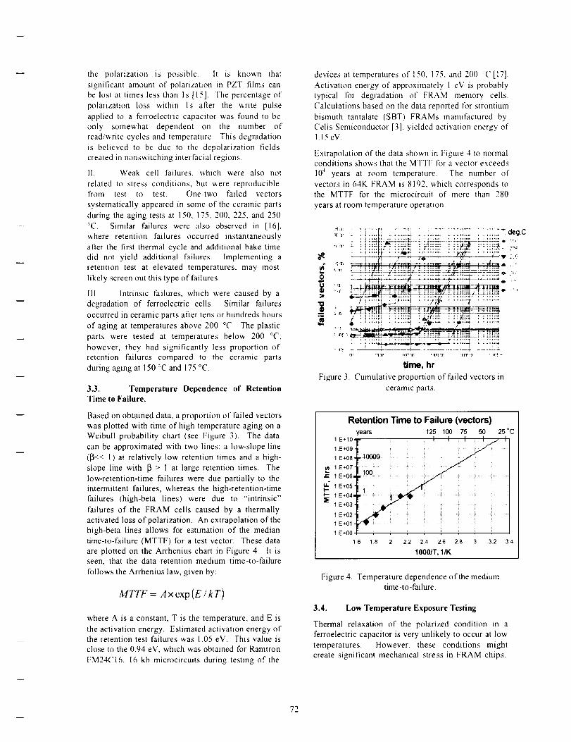
the polarizationis possible. It is knov_nthatsignificantamountof polarizationin PZT films can
be lost at times less than ls [15]. "['he percentage of
polarization loss within Is after the ,,,,rite pulse
applied to a ferroelectric capacitor was found to be
only somewhat dependent on the number of
readiv+rite cycles and temperature. This degradation
is believed to be due to the depolarization fields
created in nonswitching interracial regions.
II. Weak cell failures, which were also not
related to stress conditions, but were reproducible
from test to test One-two failed vectors
systematically appeared in some of the ceramic parts
during the aging tests at 150, 175, 200, 225, and 250
°('. Similar failures were also observed in [16],
where retention failures occurred instantaneously
after the first thermal cycle and additional bake time
did not yield additional failures. Implementing a
retention test at elevated temperatures, may most
likely screen out this type of failures.
III Intrinsic failures, which were caused by a
degradation of ferroelectric cells. Similar failures
occurred in ceramic parts after tens or hundreds hours
of aging at temperatures above 200 °C. The plastic
parts were tested at temperatures belov, 200 °C;
however, they had significantly less proportion of
retention failures compared to the ceramic parts
during aging at 150 °C and 175 °C.
3.3• Temperature Dependence of RetentionTime to Failure.
Based on obtained data, a proportion of failed vectors
was plotted with time of high temperature aging on a
Weibult probability chart (see Figure 3). The data
can be approximated with two lines: a low-slope line
(!3<< I) at relatively low retention times and a high-
slope line with 13 > 1 at large retention times. The
low-retention-time failures were due partially to the
intermittent failures, whereas the high-retention-time
failures (high-beta lines) were due to "intrinsic"
failures of the FRAM cells caused by a thermally
activated loss of polarization. An extrapolation of the
high-beta lines allows for estimation of the median
time-to-failure (MTTF) for a test vector. These data
are plotted on the Arrhenius chart in Figure 4+ It is
seen, that the data retention medium time-to-failure
follows the Arrhenius law, given by:
MTTF = A x exp (E / k T)
where A is a constant, Y is the temperature, and E is
the activation energy. Estimated activation energy ofthe retention test failures was 1.05 eV. This value is
close to the 0.94 eV, which was obtained for Ramtron
FM24('16, 16 kb microcircuits during testing of the
devices at temperatures of 150, 175, and 200 °(" [17].
Activation energy of approximately I eV is probably
typical for degradation of FRAM memory cells.
Calculations based on the data reported for strontium
bismuth tantalate (SBT) FRAMs manufactured by
Cells Semiconductor [3], yielded activation energy of
1.15 eV.
Extrapolation of the data shown in Figure 4 to normalconditions shows that the MfTF for a vector exceeds
104 years at room temperature• The number of
vectors in 64K FRAM is 8192. which corresponds to
the MTTF for the microcircuit of more than 280
years at room temperature operation
_<r ; i,; ........ ..i . :,,: ......... , dcg.C
, i , ,,_, + • . * .++1.+ • +' ++.+++ . *, • ...... ,'.: •
±:'-_v :,1 - r _I,Q. r i Y'.:m . I .... l.+ ,:_A,i ........ ii __,_+:Ai . J,-.-A
.... ,r=..,_ ...... + ...... +++..,T.++::+4-. ....... _._,++-++-_+ +++++_---.i--_.+-+.+ :+ +
'_ i, - .... _...+ l.t./+fi_ ++++...i... ---t--'x+ TX+lill
,_ i ...... !'i ...... ,f ; ."_r+++t -"+,"-+t ......
,,++,,_._,__ -+!+_ .-+-,t++_................. +n; ............
• ,:_ _ __+-+LL2_ =.... _ ........... --4-rr "q rll, 1,_ +lp , _o_ ,1_ F1Fll""J" , I'T_
time, tit
Figure 3. Cumulative proportion of failed vectors in
ceramic parts.
Retention Time to Failure (vectors)ears 125 100 75 50
1 E+10- I I
1.E+09-1 E+08• - 10000
1 E+07-e- 1 E+06=
1 E+05"
_ 1 E+04.1 E+03-
1 E+02-1 E+01
1 E+00
25 °C
16 18 2 22 24 26 28 3 32 34
1000IT, 1/K
Figure 4. Temperature dependence of the medium
time -to-failure.
3.4. Low Temperature Exposure Testing
Thermal relaxation of the polarized condition in a
ferroelectric capacitor is very unlikely to occur at low
temperatures. However, these conditions might
create significant mechanical stress in FRAM chips.
72

lhesestressescandegradethecapacitorsbyalteringthetetragonalstructureoftheperovskitelattice[13].Lowtemperatureexposuretestingwasperformedat85°Contwolotsof 5 ceramicand5 plasticparts,withinterimandfinalEMat3,28,128,373,1373and6473hourscumulativeIntermittentfailureswereobservedinceramicaswellasinplasticpartswithsomefailuresappearingduringinterimEMthatclearedupduringfollowingmeasurements.TestresultsaresummarizedinTable9.
Table9. DataRetentionTestsat-85°C
Total
time,hrs
3
28
128
373
1373
6473
RT, Ceramic Parts
hrs Failed I Failed
parts I vectors
3 1/5 1
25 2/5 3
100 0t5 0
245 1/5 I
1000 0/5 0
5110 0/5 0
Plastic parts
Failed i Failedparts vectors
0t5 0
2/5 2
1/5 1
O/5 0
3/5 5
1/5 3
3.5 Temperature Cycling
Temperature cycling can significantly degrade theretention characteristics of FRAM microcircuits. A
study [10] was performed to evaluate the effects of
thermal excursions on the remnant polarization level
in polycrystalline films in test capacitors An
excursion to elevated temperature was been found to
cause a reduction in retained polarization. Up to 60%
of the initial polarization was lost when a device was
cycled from -25 °C to +125 °C. In mother study
[20], the thermal cycle dependent retentivity problem
was attributed to pyroelectric charges that are
developed during temperature cycling.
In our evaluation 5 ceramic and 5 plastic parts were
subjected to temperature cycling from - 65°C to
150°C with dwell times of 10 minutes at each
temperature extreme. Interim and final EM were
performed at 10, 40, 140, and 425 cycles cumulative
total. All ceramic parts passed all EM. Intermittent
failures were observed in one out of five plastic parts
that failed during two interim EM, but then passed
final EM. Test results are summarized in Table 10.
These results show that the parts can sustain more
than 285 temperature cycles, without loosing stored
in formati on
Yable 10 Data Retention lest for Temperature
Cycling (- 65 _(' to ÷ 150 _C)
Total RT, Ceramic Parts
Cycles cycles Failed [Failed
parts [ vectors
10 10 0/5 0
40 30 0/'5 0
140 100 0/5 0
425 285 0/5 0
Plastic parts
Failed ] Failedparts vectors
0,_5 0
1/5 4
1/5 4
0/5 0
3.6 Total Dose Radiation Testing
Total dose radiation testing was performed on two
lots of 4 ceramic parts and 4 plastic parts, using Co-
60 irradiation source, at exposure level steps of 10,
50, and 90 krad(Si) cumulative total, in accordance
with MII,-STD-883, Method 1019 Interim and final
EM were performed at each of the steps and after
final exposure All four ceramic parts passed EM at
al all steps including final exposure level of 90
krad(Si). Intermittent failures were observed in
plastic parts that failed at some ntermediate step
levels, but then passed at final exposure step level of
90 krad(Si) Test results are displayed in Table 11.
Table I 1 Data Retention Results tbr Radiation
Testing
Total RT
dose dose
(krad) (krad)
0 0
10 10
50 4O
90 40
Ceramic parts
Failed ] Failedparts vectors
0/4 0
0/4 0
0/4 0
0/4 0
Plastic parts
Failed IFailedparts vectors
1/4 3
I/4 1
314 8
0/3 0
4.0 FATIGUE TESTING
One ceramic and one plastic part were subjected to
3×10⁷ write-read cycles to get preliminary evaluation
of the fitigue tolerance of the parts. During the
testing, parametric and functional measurements
were performed with logarithmic increments in
number of cycles to check for any parametric
changes or functional anomalies. No failures
occurred during the testing; however, some
parametric degradation was observed
73

Initialparametricmeasurementsof themicrocircuitsrevealedpatterndependenceof the operationalcurrent(I('COP).Figure5showstheeffectof the"'l"-to-"O'"proportionin vectorpatternson theoperationalcurrentmeasuredintwomicrocircuits.Inbothcasesthecurrentlinearlyincreasedwith theproportionof bit"1""vdththesameslopeof0.0053mA/%.Theresultcanbeexplained,assumingthatasignificantproportionofthemeasuredcurrentisdueto thesumof elementaryswitchingcurrentsin theferroelectriccells. Whena bit "1" is written,theelementaryswitchingcurrentisasumofa linear(ornonswitching)responseandaswitchingresponseofacell.Whenabit"0"iswritten,thecellcurrentisdueto onlynonswitchingresponse.Thepossibilitytoestimateswitchingcurrentallowsmonitoringfatigueprocessesin ferroelectriccells by comparingoperationalcurrentswithdifferentpatterns.
876[
=
o. 4
03_0 2
1
0
0 100
[] [] []
[] SN 96 C
[] SN 22 P
[] []
i i i
25 50 75proportion of bit "1", %
Figure 5. Effect of bits "'1" to "0" ratio in the test
pattern on operational current in a ceramic and a
plastic part.
rest results shown in Figure 5 indicate that the
operational currents decreased linearly with a
logarithm of number of cycles: lop = lop(0)*o.*lg(t),
where lop(0) is the initial current and ct is the slope.
Results of calculations of the slope values are shownin Table 12.
Table 12. Operational current fatigue curve slope, oq
(p,A/decade).
Pattern Ceramic Plastic
part part
-0.8234IC Cop I -67.16
ICCop0 -56.12 -1.2972
A : ICCopI-ICCop0-11.27 0.4508
_6866
_84
m
58/
1 E+02
Ceramic SN 90 Operational Currentvs. WlR cycles
;--- . _ I ii_c(;pO [
1 E÷03 1 E+04 1 E+O5 1 L÷06 1 E+O/
number of cycles
J1 E+08
a)
Operation Current vs. WIR Cycles.
1 E+O0 1 E÷01 1 E+02 1 E÷03 1F_*04 1 E+05 1 E+06 1 E+O? 1 £-+Oe
number of cycles
b)
Figure 6. Fatigue test results for (a) ceramic, and (b)
plastic parts
For both patterns ("1" and "'0"), the slope was
negative, indicating a decrease in the nonswitching
polarization. The plastic part had 50 to 80 times less
slope than the ceramic part. This was probably due
to some improvements in the process of wafer
manufacturing of dice used in the plastic parts.
[nternal examination confirmed that the plastic and
ceramic parts were manufactured using different
processes. The die size, pattern size and layouts were
different. The dice used in plastic parts were
manufactured using 1998 photomasks and the dice,
which were used in ceramic parts, were dated 1996.
For the ceramic part the difference between ICCopl
and ICCop0 decreased with time, indicating some
fatigue-related decrease of the switching polarization.
5.0 CONCLUSIONS
Data Retention characteristics of 64k FRAM
microcircuits were characterized in temperature
range from -85°C to _310 °C during retention
periods, up to several thousand hours with the
following results:
1.1. No parametric or functional failures, which
would suggest aging degradation, had
occurred during multiple ceramic and plastic
74

2.
parts testing at aging temperatures belo,,_, 250
° C
I 2 l'he observed retention test failures can be
divided in three categories:
• Random failures, which are not related to
stress conditions. Plastic parts had
approximately 15 times higher probability of
similar failures.
• Weak cell failures, which were also not
related to a stress condition, but were
reproducible from test to test. One-two
failed vectors systematically appeared in
some parts during the aging tests
Implementing a high temperature retention
test most likely could screen out similarfailures.
• Intrinsic failures, which were caused by a
thermal degradation of the ferroelectriccells. Similar failures occurred in ceramic
parts after tens or hundreds hours of aging at
temperatures above 200 °C An estimated
activation energy of the retention test
failures was 1.05 eV and the extrapolated
mean time to failure at room temperature is
more than 280 years
1 3 No parametric ot functional failures of
ceramic or plastic parts were detected during
multiple (up to 425 cycles) temperature
cycling from -65 °C to +150 °C. Both type
of parts (ceramic and plastic) withstood data
retention test with 285 temperature cycles
between writing and reading.
14 Retention test at -85 °C did not reveal any
intrinsic failures. However, some random
failures occurred both in ceramic and in
plastic parts. The long-term storage (more
then 5000 hrs retention time) of the parts did
not result in any parametric or functional
degradation.
1.5 No retention, parametric, or functional
failures occurred with ceramic parts during
the radiation tests with cumulative total dose
of 90 krad (St). Plastic parts had some
random retention test failures.
Operational current measurements with different
patterns allow for estimation of the levels of
switching and non-switching polarization in theferroelectric cells. The difference between these
two currents depends on the average remnant
polarization and can be used for monitoring
degradation processes in the memory cells.
However, additional analysis should be
performed to reliably establish the relationship
bet',seen the operational currents and the le,_el of
cell polarization.
Multiple write-read cycling (up to 3x10 v) during
fatigue testing of plastic and ceramic parts did
not result in any parametric or functional
failures. However operational currents linearly
decreased with the logarithm of number of
cycles, thus indicating fatigue process in the PZT
films. Plastic parts manifested significantly
smaller changes in operational currents, _hich
could be due to the different die lots used in
manufacturing of these parts
Test results confirmed that PZT-based FRAM
microcircuits potentially might have perfect
retention and virtually fatigue-free characteristics
over a wide interval of temperatures and write-
read cycles This. as well as a high radiation
tolerance, low power and ',,,'rite time makes these
devices very attractive for space applications.
However, further improvements in the
manufacturing process and'or testing and
screening system are necessary to reduce random
soft failures in these devices
6. ACKNOWI.EDGEMENTS
The authors would like to thank the personnel of the
Parts Laboratory of the Goddard Space Flight
Center/0SS: in particulaz Sam Archer-Devis and
Alix Duvalsant for thei_ support
References
[11 A.Sheikholeslami, P.Gulak, A survay of circuit
innovations in ferroelectric memories, Proc.
[EEE, v.88, N5, 2000, pp.667-689.
[2] K.F. Strauss, et al, "'Overview of radiation
tolerant unlimited write cycle non-volatile
memory", Aerospace Conference Proceedings,
2000 IEEE, Volume: 5,2000, pp. 399 -408.
[3] S.C. Philpy, et al., "'Ferroelectric memory
technology for aerospace applications", IEEE
Aerospace Conference Proceedings, 2000, v. 5,
pp. 377 -383.
[4] J.M. Benedetto, et al.., "Radiation evaluation of
commercial ferroelectric nonvolatile memories",
IEEE Transactions on Nuclear Science, v. 38,
Issue 6, Part: 1, Dec. 1991, pp. 1410 -1414.
[5] E.M. Philofsky, "FRAM-the ultimate memory",
Sixth Biennial IEEE International Nonvolatile
Memory Technology Conference, 1996, pp.: 99
104.
75

[6] J.J.Lee,et al.. "'ElectrodecontactsonferroelectricPZTandSBTthinfihnsandtheirinfluenceonfatigueproperties",J.Appl.Phys,v.78,#8,1995,pp5073-5077.
171J.Chen,et al., "'Compositional control of
ferroelectric fatigue in pervoskite ferroelectric
ceramics and thin films". J Appl Phys, v76, #9,
1994, pp5394-5398.
[8] J. ('hen, et al, "'Polarization fatigue in perovskite
l'erroelectric ceramics and thin- films",
Proceedings of the Eighth IEEE International
Symposium on Applications of Ferroelectrics.
ISAF'92,1992, pp 111 115.
191 D. E. Fisch, et al., "'Analysis of thin film
ferroelectric aging", IEEE, IRPS. 1990, pp 237-242.
[lO]Gregory, A_ et al.., "'Thermal stability of
ferroelectric memories", 30th Annual
Proceedings, International Reliabilib, Physics
Symposium 1992., Page(s): 91 -94.
[11 ] D Hadnagy, "'Making ferroelectric memories".
The industrial physicist, Dec 1999, pp.26-28
1121Woo Sik Kim et al, "'Fabrication andcharacterization of Pt-oxide electrode for
FeRAM application" International Conference
Microprocesses and Nanotechnology. 2000
Page/s): 186 187
1131EM Philofsky, et al., "The evolution of
hydrogen from plastic molding compound and
it's effect on yield and reliability of ferroelectric
memories", 36th Annual Proceedings,
International Reliability Physics Symposium
1998, Page(s): 232 237.
[14] W.LWarren, et al., "'Polarization suppression in
Pb(Zr,Ti)O_ thin films", JAppl. Phys, v.77, (12),
1995, pp. 6695-6701.
[15]J.M. Benedetto, et al., "'Effect of operating
conditions on the fast-decay component of the
retained polarization in lead zirconate titanate
thin films", J. Appl. Phys., v. 75 (1), 1994, pp.
460-466.
[16]S.D Traynor, "'Polarization as driving force in
accelerated retention measurements on
ferroelectric thin films", 1998, pp. 15-18,
[171 Ramtron Application Note: FRAM* Technology
Backgrounder, Technology notes,
www.ramtron.com
analysis and evaluation o1 hybrids, microcircuits and
discrete active and passive components. Currently,
he is involved in several projects aimed to evaluate
new technologies and components tbr space
applications.
Dr. Teverovsky is an author of more than 50
technical publications and holds several patents on
test techniques
Alexander Teverovsky Alexander Teverosky
received Ph.D in electrical engineering from Moscow
University of Electronics, Russia. He worked in
Moscow Institute of Electronic Machine Building
developing techniques and specializing in reliability
physics of semiconductor devices. Dr. Teverovsky
jointed Goddard space flight center parts analysis lab
in 1994 as a senior failure analyst performing failure
76

l/
Radiation Response of Emerging FeRAM
TechnologyD. N. Nguyen and L Z. Scheick
Ahstra('t---- The test results of measurements performed
on two different sizes of ferroelectric RAM (FeRAM)
suggest the degradation is due to the low radiation
tolerance of sense amplifiers and reference voltage
generators which are based on commercial CMOS
technology. This paper presents TID testing of 64KbRamtron FMI608 and 256Kb Ramtron FMI808.
1. INTRODUCTION
F erroelectric memories have received moreresearch attention in recent years. In term of the
number of inventions granted by the U.S patent office,
there were 120 for the year of 1999 alone. Fast
programming time with low power consumption and the
rising demands of smart cards and digital cameras have
driven the recent activity. In addition, many deep space
and near earth missions are looking for alternatives to
traditional NVM Floating-gate memories such as flash
memories and EEPROMs with larger storage capability
currently dominated the digital camera applications are
due in part to its mature process technology. But
ferroelectric memories possess superior features over
floating-gate devices. These are write-access time and
overall power consumption [1]. Table I compares flashmemories, EEPROMs and ferroelectric memories.
Digital cameras for use in future space rovers andminiature smart instruments will benefit from the fast
frequent writes and low power usages of ferroelectricmemories.
In addition to fast write requirements, banery-less smart
cards operate from power supplied by an r-f signal fromthe card reader.
II, DEVICES DESCRIPTIONS
A Ferroelectric Technology
The ferroelectric effect is characterized by the remnant
polarization that occurs after an electric field has been
applied. The unique chemical atomic ordering of these
materials allows a single ion to change its physical
location. Figure 1 shows simplified models of a
ferroelectric material. The center atom (zirconium or
titanium) will move into one of the two stable states
upon an external applied electric field. After theexternal electric field is removed, the atom remains
polarized in either state; this effect is the basis of the
ferroelectric as a nonvolatile memory. An electric field
can reverse the polarization state of the center atom,
changing from a logic state "0" to "1" or vice versa.
m,-.,_stateo T
Positwe Electrnc Faeld
Positive Polarization
State 1 1 _ ; _lxl(Zrgerl
Binary 0 PbNegative Electric Field
Negative Polarization
TABLE I
Comparison of Nonvolatile MemoriesFeRAM EEPROM Flash
Write (ns) 100 106- 107 104- 10_
Write Voltage I-3V 12-18V 12-2 IVWrite cycles >10 t2 10s l0 s- 106Overwrite Yes No No
The work described in this paper was carried out by the Jet Propulsion
Laboratory., California Institute of Technology, under contract with theNational Aeronautics and Space Administration, Code AE, under the NASA
Microelectronics Space Radiation Effects Program (MSREP),
The authors are ',,_,ith the Jet Propulsion Laboratory, California Institute of
Technology, Pasadena, California, 91109, USA
Fig I. Two stable states in a ferroelectric material
The ferroelectric thin-film material of RAMTRON
product is lead-zirconate-titanate (PZT). Figure 2 shows the
hysteresis loop exhibited by a PZT ferroelectric capacitor.The total charge for a relaxed "'0" state is Q_ and -Q_ for a
relaxed "1" state. By applying a negative voltage across the
capacitor, a "0" state can be changed to "1", andconsequently the total charge on the capacitor is reduced by
2Q_. With a positive voltage across the capacitor, a "'1"canbe switched back to"0", and the total charge restores to _Q_.
]'he nonvolatile polarization, P,,, is the difference betweenthe relaxed states, the charge density that can be sensed by
the sense amplifier circuitry
77
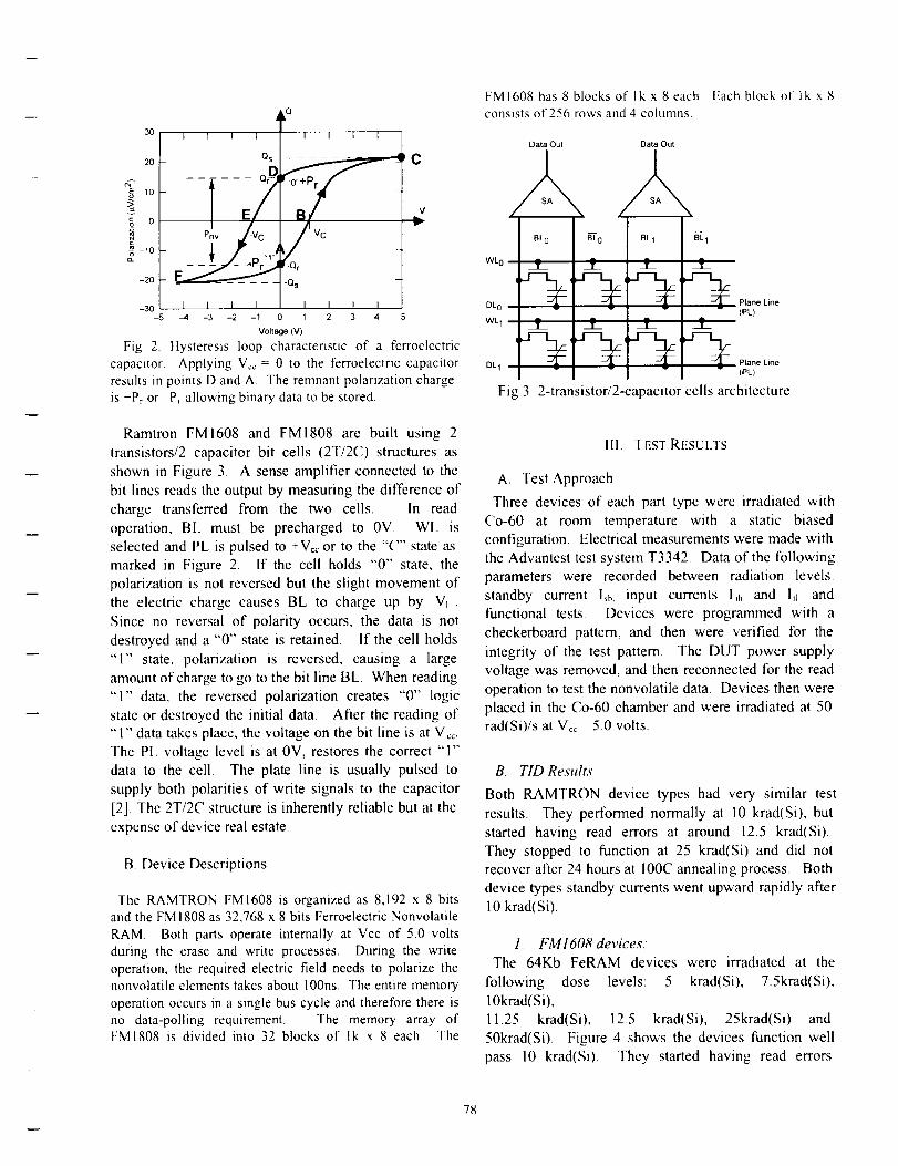
30
2O
>__ 0
-10
-20
-30
I ; I _ t Q I I I I
Qs
m
Pnv /Vc J Vc
_Os --
I I I I I I I I
C
-5 _4 -3 -2 -1 0 1 2 3 4
Voltage (V)
Fig 2. ltysteresis loop characteristic of a ferroelectriccapacitor, Applying V_ = 0 to the ferroelectric capacitor
results in points D and A. The remnant polarization chargeis +Pr or Pr allowing binary data to be stored.
Ramtron FM1608 and FMI808 are built using 2
transistors/2 capacitor bit cells (2T/2C) structures as
shown in Figure 3. A sense amplifier connected to the
bit lines reads the output by measuring the difference of
charge transferred from the two cells. In read
operation, B[. must be precharged to 0V. WL is
selected and PL is pulsed to + Vc_ or to the "C" state as
marked in Figure 2. If the cell holds "0" state, the
polarization is not reversed but the slight movement of
the electric charge causes BL to charge up by V_.
Since no reversal of polarity occurs, the data is not
destroyed and a "0" state is retained. If the cell holds
"l" state, polarization is reversed, causing a large
amount of charge to go to the bit line BL When reading
"1" data, the reversed polarization creates "0" logic
state or destroyed the initial data. After the reading of
"1" data takes place, the voltage on the bit line is at V_.
The PL voltage level is at 0V, restores the correct "1"
data to the cell. The plate line is usually pulsed to
supply both polarities of write signals to the capacitor
[2]. The 2T/2C structure is inherently reliable but at the
expense of device real estate.
B Device Descriptions
The RAMTRON FMI608 is organized as 8,192 x 8 bitsand the FM1808 as 32,768 x 8 bits Ferroelectric Nonvolatile
RAM. Both parts operate internally at Vcc of 5.0 voltsduring the erase and write processes. During the write
operation, the required electric field needs to polarize thenonvolatile elements takes about lOOns. The entire memory
operation occurs in a single bus cycle and therefore there isno data-polling requirement. The memory array ofFMIS08 is divided into 32 blocks of lk x 8 each. The
FM1608 has 8 blocks of Ik x 8each. Each blockof lk x 8consists of 256 rows and 4 columns.
Data Out
2,B[ o
WL 0 -- __
DL0 i _
WL 1 -- __
DL1 I J_
_o
i
-%i
-%
Data Out
BLI _1
EL EL
___ __k
Plane Line
(PL)
Plane Line
(PL)
Fig 3 2-transistor/2-capacitor cells architecture
III. TEST RESUHS
A rest Approach
Three devices of each part type were irradiated with
('o-60 at room temperature with a static biased
configuration. Electrical measurements were made with
the Advantest test system T3342. Data of the following
parameters were recorded between radiation levels:
standby current l_b, input currents l,h and I,_. and
functional tests. Devices were programmed with a
checkerboard pattern, and then were verified for the
integrity of the test pattern. The DUT power supply
voltage was removed, and then reconnected for the read
operation to test the nonvolatile data. Devices then were
placed in the Co-60 chamber and were irradiated at 50rad(Si)/s at V¢_- 5.0 volts.
B. TID Results
Both RAMTRON device types had very similar test
results. They performed normally at 10 krad(Si), but
started having read errors at around 12.5 krad(Si).
They stopped to function at 25 krad(Si) and did not
recover after 24 hours at 100C annealing process. Both
device types standby currents went upward rapidly after
10 krad(Si).
1. FM1608 devices.
The 64Kb FeRAM devices were irradiated at the
following dose levels: 5 krad(Si), 7.5krad(Si),
10krad(Si),
ll.25 krad(Si), 12.5 krad(Si), 25krad(Si) and
50krad(Si). Figure 4 shows the devices function well
pass 10 krad(Si). They started having read errors
78

around12.5krad(Si)whenthestandbycurrentwentintomA range•Butalterrewritewiththe same pattern, the
parts were functional again At 25krad(Si), devices
fhiled to read all 8,192 cells. DUTs were programmed
with all zeros and then read back. None of the 8,192
locations had registered a "0" state. At 50krad(Si), the
input current l,h is marginally over the specifications
limit of 10p.A, precisely at 12.31aA
10000
• _ ] Failed Functional
_._ 1000 _'_ q , Stuck at 1 |_ Few Read Errors, but OK
100 j_ J After Rewrde
J10<
1 I I I I I10 20 30 40 50
Total Dose [krad(Si)]
Fig 4. Standby Current vs. Total Dose of 64Kb FeRAM
60
Figure 5 shows standby currents of two post-irradiatedDUTs after more than 100 hours unbiased room
temperature anneal versus the number of write/read
cycles Serial number 4278 part had 2 read errors prior
to the cycling test. The two read errors stayed until the
end of the 9 millionth cycles
c
¢D
1000OI I I I I I I I I
[ 2 ReadErrors ]
1000 I
100 C1-
10 + 4278_post_12 5k
I --[_- 4275 ,oosl 10k
f I I I I I ] I I I1E6 2E6 3E6 4E6 5E6 6E6 7E6 BE6 9E6
Number of Cycles
Fig 5. Standby current vs. cycling of FM 1608
2 t:M1808 devices.
The 256Kb FeRAMs were exposed at the following
dose levels: 5 krad(Si), 75krad(Si), 10krad(Si),
12.5krad(Si), and 25 krad(Si) Figure 6 illustrates its
response of standby current versus the total dose, Like
the FMI608 parts, DUTs passed at 10 krad(Si) with
standby current recorded under 20 IuA Three read
errors were observed at 125 krad(Si) and standby
current started going upward to 100 /aA range
,0ooo IT,reel .aad[ /
1000
100
co10
I 1 I 1 I1
0 5 10 15 20 25 30
Total Dose [krad(Si)]
Fig 6 Standby current vs. Total Dose of255Kb FeRAM
IV CONCLUSIONS
The FRAM is affected and seems to have TID
problems at around 12.5 krad(Si) and ceases to function
at 25 krad(Si). Since writing to FeRAM cells is a direct
overwrite process, there is no pre-erase and polling to
monitor and keep track of how many write errors
accumulated during programming. Ferroelectric thin
films have been seen to be inherently resistant to
ionizing radiation [3]. In order to operate normally in a
radiation environment, ferroelectric technology will
need to combine with a radiation hardened CMOS
process in order to withstand higher TID levels.
Samples of devices of large sizes, 1Mb to 32Mb are
being procured. Samples from other manufacturers also
are being investigated.
V. REFERENCES
[1] A. Sheikholeslami and PG Gulak, "A survey of circuit mnovalions in
ferroelectric random-access memories," 2000 Proceedm._s o[ the IEt'E,
vol. 88, no. 5, pp 667-689, May 2000.
[2] E.M. Philofsky, "FRAM-the ultimate memory," hlt'l NonVolatile
Memory Technolo&v Conl?rence 1996, pp. 99-104
[3] S.C. Lee, G. Teovvee, R.D. Schnmpf. D.P. Birnie, lit, DR Uhlmann,
and KF. Galloway, "Total dose radiation effects on Sol-Gel den'_ed PZT
thin films," IEEE l'rans On Nucl Set . vol 39. no 6. pp 2036-2043,
December 1992.
79
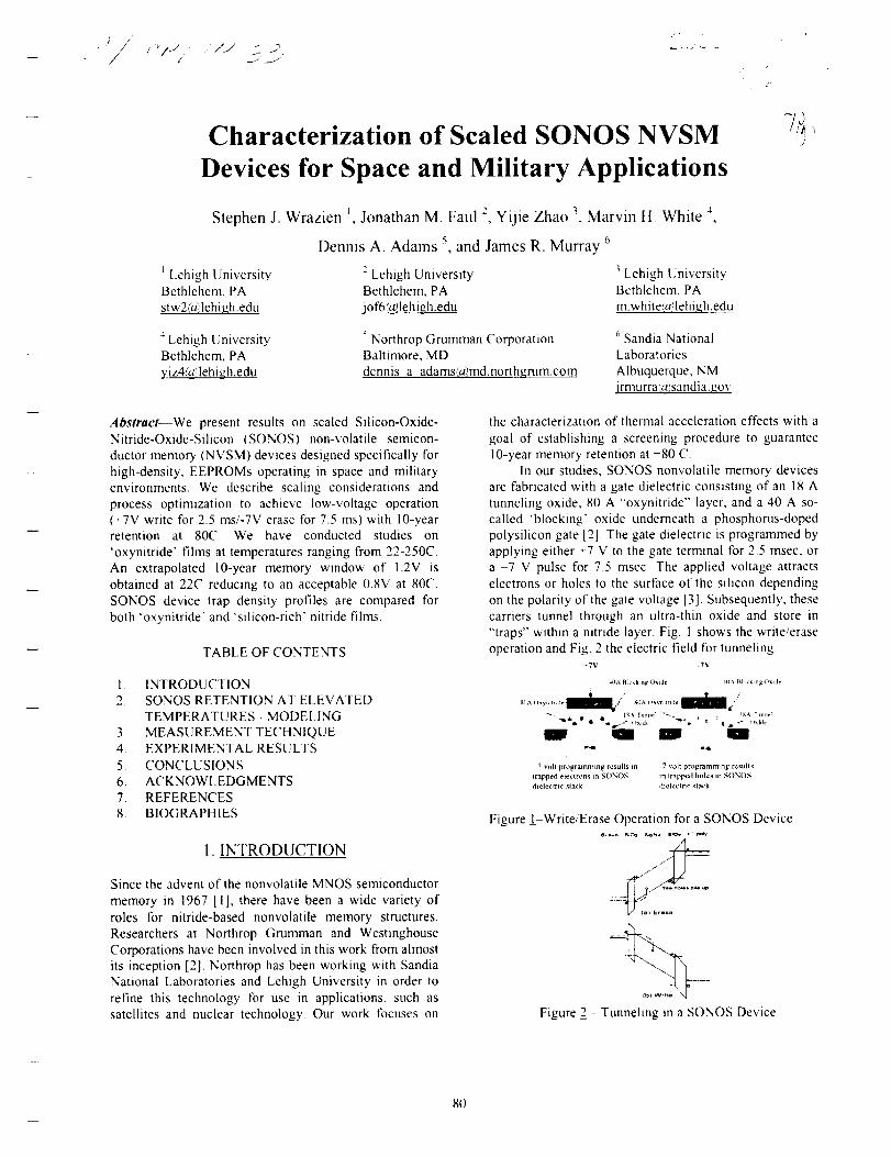
/( _/2J
/
/
Characterization of Scaled SONOS NVSM
Devices for Space and Military Applications
71'_ "/
Stephen J. Wrazien _, Jonathan M. Faul : Yijie Zhao 3 Marvin l I. White _
Dennis A. Adams 5, and James R. Murray 6
t Lehigh University -' Lehigh University _Lehigh UniversityBethlehem, PA Bethlehem, PA Bethlehem, PA
stw2(a)lehi.c_h.edu jof6(a!lehigh.edu m white(@ehi,_h.edu
4Lehigh UniversityBethlehem, PA
yiz4(ailehigh.edu
Northrop Grumman CorporationBaltimore, MD
dennis a adams(a;,md.northgrumcom
6Sandia NationalLaboratories
Albuquerque, NMirmurra',alsandia.t_ov
Abstract--We present results on scaled Silicon-Oxide-Nitride-Oxide-Silicon (SONOS) non-volatile semicon-
ductor memory (NVSM) devices designed specifically forhigh-density, EEPROMs operating in space and militaryenvironments. We describe scaling considerations andprocess optimization to achieve low-voltage operation( +7V write for 2.5 ms/-7V erase for 7.5 ms) with 10-yearretention at 80C. We have conducted studies on
'oxynitride' films at temperatures ranging from 22-250C.An extrapolated 10-year memory window of 1.2V isobtained at 22C reducing to an acceptable 0.8V at 80C.SONOS device trap density profiles are compared for
both 'oxynitride' and 'silicon-rich' nitride films.
TABLE OF CONTENTS
1. INTRODUCTION2. SONOS RETENTION AT ELEVATED
TEMPERATURES - MODEI3NG
3. MEASUREMENT TECHNIQUE4. EXPERIMENTAL RESULTS
5. CONCLUSIONS6. ACKNOWI,EDGMENTS7. REFERENCES8, BIOGRAPHIES
1. INTRODUCTION
Since the advent of the nonvolatile MNOS semiconductor
memory in 1967 [1], there have been a wide variety ofroles for nitride-based nonvolatile memory structures.Researchers at Northrop Grumman and Westinghouse
Corporations have been involved in this work from almostits inception [2]. Northrop has been working with SandiaNational Laboratories and Lehigh University in order torefine this technology for use in applications, such assatellites and nuclear technology. Our work focuses on
the characterization of thermal acceleration effects with a
goal of establishing a screening procedure to guarantee10-year memory retention at +80 C.
In our studies, SONOS nonvolatile memory devicesare fabricated with a gate dielectric consisting of an 18 A
tunneling oxide, 80 A "oxynitride" layer, and a 40 A so-called 'blocking" oxide underneath a phosphorus-doped
polysilicon gate [21. The gate dielectric is programmed byapplying either +7 V to the gate terminal [br 2.5 msec, ora -7 V pulse for 7.5 msec. The applied voltage attractselectrons or holes to the surface of the silicon depending
on the polarity of the gate voltage [3]. Subsequently, thesecarriers tunnel through an ultra-thin oxide and store in"traps" within a nitride layer. Fig. 1 shows the write/eraseoperation and Fig. 2 the electric field for tunneling.
_-TV -7_
+0A Fllockin_ OxltJ¢ ;o.\ t_.[,,ckmgOxlde
"-. lg _, luanel "-.. i , [unnel_,t,.ll • • oxide "1" J "
Dw.a m41,
7 volt programming results In -7 volt programming r¢_ulls
flapped eleclrons m SONOS m trapped holes m SONOS
dielectric slack dlelectnc stack
Figure 1-Write/Erase Operation for a SONOS Device
./
Figure 2 Tunneling in a SONOS Device
8O

_' 1.5
• 1.0
0> 0.0
"6 -0.5
8 -lo
,, 22*C _"I_ %u._rl
x 125"C
+ 150+C
A 175+C=.,._ .t_B,fl_i,_5 A
_1i'_'_1t_i_1_ Xn = 62 A
_= Xob= 42 A
-1.5 -4 -2 0 2 4 0 610 10 10 10 10 1
Read delay time trd (8ec)
Figure 3 Threshold Voltage decay vs. Temperature for a
"silicon-rich' Scaled SONOS NVSM Device. The device
has experienced 10 _ erase/write cycles. The initial V-rH is
set with a series of erase/write pulses of_+7V lmsec [13].
2. SONOS RETENTION AT ELEVATED
TEMPERATURES MODELING
The decay of the charge stored in the nitride layer at
room temperature has been modeled by a number of
investigators, such as White and Cricchi [4], Lundkvist,
Lundstrom, Svensson [5], Roy and White [6], Kamagaki
and Minami [7,8], and Hu and White [9]. These models
invoke back tunneling of charge from the nitride to the
semiconductor substrate. An internal field due to trapped
charges enhances the process of tunneling.
The characterization of charge trapped in a nitride
dielectric at elevated temperatures had been investigated
for SNOS devices by Sandia researchers [10,11] and
researchers from Chalmers University in Sweden [12].
Recently, with the advent of scaled SONOS devices,
Lehigh researchers Yang and White [13] have examined
the temperature dependence with an amphoteric trap
model, which attributes the electron and hole charge
storage to a silicon dangling bond. Their results, shown in
Fig. 3, indicate the trapped 'electrons' in the nitride layer
are thermally excited at elevated temperatures and 'back
tunnel' through an ultra-thin tunnel oxide to the silicon.
In contrast, the distribution of trapped 'holes' is
influenced very little with increasing temperature. This
result was explained by suggesting the activation energy
for the electron traps lies closer to the conduction band
edge in the silicon nitride than the activation energy for
hole traps to edge of the valence band in the silicon
nitride as shown in Figure 4.
Using this trap model, Yang and White [13] derived
an expression for the charge trapped in the nitride,
p,, ( x, Er,+, t) = - qg( x, El:4)/- (I)
where EtA is the energy level of the trap, f is the trap
occupancy function for electrons, and g(x,ErA) is the
density of traps in the nitride (traps/cm_eV) at a distance
"x' from the tunnel oxide-nitride interface into the nitride.
excess electron slate
EF5 .... : ..... EFG
S O N O $
excess hole stale
E F£ L];
s 0 oN
.... EF_
Figure 4 Storage of Nitride Trapped Charge
The charge stored in the nitride causes a shift in the
threshold voltage of the device, AVrH, which can be
written as l 13 ],
=-2.3k_TX, ( _ + X°B ]g(E,:4 )81og(t) ' _,2ev eox)
(2)
where Xx and X(m are the thicknesses of the nitride and
blocking oxide, respectively, while Ex and e(>x are the
dielectric constants of the nitride and blocking oxide,
respectively. Equation (2) assumes a uniform distribution
of nitride traps and the activation energy responsible for
the decay rate is [13]
E[,_ = kl+Tln(AT2t) (3)
where A is a constant given as
2ran k#/A = 2_,, / (4)
where c, is the trap capture cross-section, m* the effective
electron mass in the nitride and 'h' is Planck's constant.
These relationships were used to interpret measurements
of retention at elevated temperatures for retention times
out to 10 s seconds for the written state of a scaled
SONOS device (See Fig. 3). Since the thermal activation
energy of electron traps is near the conduction band edge,
the electrons are thermally excited from these traps and
back-tunnel through the tunneling oxide. Eqn. (3) shows
the trap energy may be probed at a given temperature by
measuring the slope of the decay characteristics as a
81

function of retention time. The capture cross-section, Gn,may have temperature dependence.
3.0
g2.0
'u1.o
_'";'° °'%,.,. 175°C
°, o
'Qt
Xot= 15 A "°',,Xn = 62 A "1,,.%,,.Xob=42A
-4 -2 0 2 4 610 10 10 10 10 10
Read delay time trd (sec)
Figure 5 Threshold Voltage decay versus retention timefor a Scaled SONOS NVSM device at T = 175C. The
device is fabricated with a 'silicon-rich' nitride [13].
Using Eqns. !-4, the decay rate of the threshold voltage[Fig 5] was used to extrapolate the trap profile in thenitride of the silicon-rich nitride, as shown in Fig. 6.
•r 3.0>
O
ra
2.0 _'r3
1.0rl
Lq_ _
0.0 , , ,0.7 0,9
-3Q
nrl
B B
D
i i i i
m 1.1 1.3 1.5
Trap energy level, E;A(eV)
Figure 6 Nitride Trap Density versus Energy for a ScaledSONOS NVSM device with a silicon-rich nitride [[3].
3. MEASUREMENT TECHNIQUE
Retention measurements at elevated temperatures
are performed at the wafer level. As in the experiments ofYang and White, we use a hot chuck, ring probe stand,oscilloscope and an analog circuit [3,14] controlled by adesktop PC. The PC controls the oscilloscope through aGPIB interface with programs written in a LabVIEW rMenvironment. Fig. 6 illustrates a block diagram of theexperimental set-up for dynamic measurements. Thesemeasurements include Erase/Write, data retention andendurance measurements as a function of temperature. Ifwe include radiation performance, then these tests are theultimate tests for NVSM devices from a user's standpoint.
The FPGA-based measurement system in Fig. 7 canexecute all of these measurements. The function generatoris designed and simulated with XILINX FoundationSoftware. The bit-streams are generated and downloadedto the FPGAs through a parallel download cable. Theanalog detection circuit, under the control of the specific
erase/write/read pulses sets the operational modes to theSONOS device under test (DUT) and determines the
change of the memory-state of the SONOS nonvolatilememory transistor. The TEK460 oscilloscope digitizes theanalog threshold voltage output and sends the latter to thecomputer (P('). The data is filtered and averaged with aLabVIEW rM program on the computer and displayed onthe monitor in real time.
The SONOS retention characteristics are monitored
by applying programming pulses to the device, waiting acertain time t_,and then forcing a constant current throughthe device and measuring the source voltage of the deviceas shown in the analog Detection Circuit of Fig. 8.
GAs Design
i Soft_at.e ] Data Proce_hlg
Figure 7 A Block Diagram of the Experimental Setup forDynamic Erase/Write/Read Measurements [3].
SW-IRd
VE Vw DUI
SW-2
RI "-, RI
.....-_1-+ sw-3-, _ ]t ::--7.4,, 'Vref I
....-IH" o._ vo_, I
Isw., q_.. I
_,,__.] R, j.
RI ! RI
Figure _8A constant-current, threshold-voltage detectioncircuit implemented with switches (SW) controlled byFPGAs[3,14] The threshold voltage is monitored at Vout.
82

The measurements are performed on a hot chuck, which
controls the temperature of the measurement environment
and the wafer, as shown in Figs. 9 and 10.
Figure 9 SONOS Wafer & tim Chuck
Figure 10 Close-up View of Hot-Chuck Probes on Wafer
The hot chuck is held at temperatures of 22 C, 80 C,
150C, and 250 C. The hot chuck used to collect this data
has been operated routinely at temperatures up to 400 C.
Due to this wear on the hot chuck, the surface where the
wafer is placed is no longer planar. This created some
difficulty in making good contacts with the probes onto
the terminals of the device. When the device is heated and
cooled, there is a degree of vibration associated with the
operation of the hot chuck. When the temperature is
increased to 125 C, the probes, which make contact on the
device expand, and often slide offofthe contact windows,
scratching the device, and losing contact with the
appropriate device terminals - especially for long-term
retention measurements to 104 seconds. We compensate
for these effects with special expansion probes and using
smaller sections of the wafers. The smaller pieces are not
affected by, the hot chuck surface or by vibrations in the
laboratory.
4. EXPERIMENTAL RESULTS
In this section, we describe retention measurements
at Lehigh University on SONOS devices from the
Northrop Gmmman Corporation 0.8 um CMOS/SONOS
1M EEPROM project. The 'oxynitride' storage dielectric
contrasts with devices fabricated with a "silicon-rich'
nitride. The thermally activated SONOS retention model
is applied using Eqns 1-4 to the retention data of
'oxynitride' SONOS devices taken at elevated
temperatures to extract the energy distribution of the
electron traps in the nitride The retention measurements
are performed, as described above, at temperatures of 22,
80, 150, and 250 C. A hot-chuck probe stand regulates the
temperature. The SONOS devices are programmed with a
7V pulse applied to the gate for 2.5msec and erased with a
7V pulse applied to the gate for 7.Smsec. The threshold
voltage of the device is read for times ranging from 10 7 to
103 seconds.
The threshold voltage of the device in the Write and
Erase states at elevated temperatures is shown in Fig. 11.
The results demonstrate the decay rate of the written state
is affected by increasing the temperature.
2s ==: i i i
2015
0s ....Zii.i 00
¢ _o.s-10
-1 5 : :
1 E-07 1 E-05 1E-03 1 E-01 1 E+01 1 E+03
Time is)
Figure 1_.1.1- VTI ! VS time at various temperatures for an
Oxynitride SONOS NVSM Device. The Write (excess
electron) state of the device is affected by temperature. In
contrast, the Erase (excess hole) state displays very little
temperature sensitivity.
The Write state threshold voltage decay rate increases as
the temperature increases. The Erase state decay rate is
virtually unchanged These trends are the same for both
the 'oxynitride' [Fig. 11] and 'silicon-rich' nitride films
[Fig. 3]. In both films we observe, for Write and Erase
states, a small initial shift of the threshold voltage with
increasing temperature.
83

Threshold Voltage Versus Time at Elevated
Temperatures - NGC Lot #.63850D - wafer #2
25
2.0_
15
_1o05
O0
-1 0
-15
1E+O0 1E+02 1E+04 1E+06 1E+08 1E+10 1E+12
Time (s)
Figure 12 - Extrapolated VIII VS Temperature
Long-term retention with temperature and radiation
is of concern for space and military applications. The
retention data has been extrapolated as shown in Fig. 12.
At 3xlO _ sec ( 10 years) and room temperature (22C) we
have a 1.2V window. At 80C the window has decreased
to 0.8V at 10 years and at 150C the window decreases to
0.3V. The data indicates these SONOS devices should be
acceptable for 7 V programming and 10 year memory
retention applications for operating temperatures below
125 C Further optimization is continuing for the 1Mb
SONOS EEPROM project.
The trap density in the nitride layer of the SONOS
device is determined as a function of trap energy using
Eqns. 1-4. Eqn. 3 is used to calculate the energies of the
traps in the nitride layer. At 250 C the trap energy ranges
from 0.6 eV to 1.43 eV. Eqn. 2 is used to calculate the
density at points along the threshold voltage curve. The
change in threshold voltage divided by the logarithm of
the change in time is calculated at each decade of time.
The electron trap density, g(EIA), is plotted versus trap
energy, E,A, as shown in Fig. 13.
[/ "I
/ \
[+Write 250 C]
06 08 10 12 14 16
Trap energy level, ETa, (eV)
Figure 13 - SONOS Oxynitride Trap Density, g(E[A), vs
trap energy, E_ ,_, for the Write (excess electron) state.
The electron trap density tbr the "oxynitride" film
peaks at 1.1 eV below the edge o1" the nitride conductionband - similar to the 'silicon-rich' nitrides film shown in
Fig. 6. The trap density of the 'oxynitride" fihn is less
than the 'silicon-rich' nitride film. This expected as the
presence of oxygen will "tie-up' silicon dangling bonds,
which cause the memory traps in the nitride.
5. C()NCL[JSI()NS
The temperature effect on the threshold voltage of
scaled (7V prograrnming) SONOS "oxynitride" NVSM
devices has been investigated At elevated temperatures,the Write state threshold voltage decay rate, 0V rn/Olog(t),
of 'oxynitride' and "silicon-rich' nitride SONOS devicesincreases with increasing temperature, while the Erasestate threshold voltage decay rate remains unchanged. We
see from Fig. 12 the extrapolated memory retentionwindow at 3 x 10* sec (10 years) and 22C is 12V, a 0.8Vwindow at 80C, and a 0.3V window at 150C. We will
take longer-term retention data in the future to see if thereis a change in the decay rates, since the electric fields will
be modified in the device with the loss of memory charge.
The nitride trap density is extrapolated from the
decay rate of the Write state at 250 C. This allows us tosee the trap distribution within the 'oxynitride' band gap.
In previous studies of elevated temperature affects, Yangand White [13] have extrapolated the electron trap densityfor a SONOS device with a 'silicon-rich' nitride layer at175 C as shown in Fig. 6. The trap density for a silicon-
rich nitride layer is roughly three times greater than thedensity for an 'oxynitride' layer as shown in a comparison
chart of Fig. 14. The 'oxynitride' and "silicon-rich' nitride
trap densities peak at the same activation energy, 1.1 eV
_25
.8_2
.8_.., 1
_05
0
04
|
Silicon-rich /
Nitride_ .....
[_,,-WriCe 250_ _' ii
• ¥=ng175 ! i'
/ •
Oxynitride /
06 08 10 12 14 16
Trap Energy Level, Er. {eV)
Figure 14 - A Comparison of Trap Densities in 'silicon-rich' and 'oxynitride' SONOS NVSM devices.
These preliminary measurements on scaled SONOS
NVSM devices support the validity of high temperature
screening measurements in the determination of long-term
retention.
84

6. ACKNOWLEDGEMENTS
The authors would like to thank the Department ofEnergy, the Army Space and Defense and MissileCommand in I luntsville, Ala., the National ScienceFoundation, and Northrop Grumman Corporation for their
continual support of SONOS NVSM technology.
7. REFERENCES
[1] tl.A.R. Wegener, A. J. Lincoln, II. C. Pao, M.R.O'('onnel, and R. E.Oleksiok, "'Metal Insulator Semicon-
ductor Transistors as a Nonvolatile Storage", 1967 IEEEInternational Electron Devices Meeting (IEDM), Abstract59, Washington, D.C.[2] D. Adams, J. Murray, and M.tl. White, "SONOSNonvolatile Semiconductor Memories for Space andMilitary Applications", NVMTS, San Diego, CA, 2001[31 J. Bu and M H White, "Design Considerations inScaled SONOS Nonvolatile Memory Devices", Solid-State Electronics, 45, 113 (2001).[4] M. H. White and J. R. Cricchi, "Characterization of
Thin-Oxide MNOS Memory Transistors", IEEE Trans.Electron Devices, ED 19, 1280 (1972).
[5] L. Lundkvist, I. Lundstrom, C. Svensson, "Dischargeof MNOS Structures", Solid State Elect, 16, 811(1973).
[6] A. Roy and M. H. White, "'Determination of theTrapped Chafe Distribution in Scaled Silicon NitrideMONOS Nonvolatile Memory Devices by TunnelingSpectroscopy, Solid-State Electronics, 34, 1083 (1991).[7] Y. Kamagaki, S. Minami, tt. Kato, "A New Portrayalof" Electron and Hole Traps in Amorphous Silicon Nitride,J. Appl. Phys., 68,2211, (1990).[8] Y. Kamigaki, S. Minami, T. Hagiwara, K Furusawa,T. Furuno, K. Uchida, M. Terasawa, and K. Yamazaki,"Yield and reliability of MNOS EEPROM products,"IEEE J. Solid-State Circuits, 24, 1714 (1989).
[9] Y. Hu and M. H. White, "Charge Retention in ScaledSONOS Nonvolatile Semiconductor Memory DevicesModeling and Characterization", Solid-State Elect., 36,1401 (1993).[10] S. I,. Miller, "Effect of Temperature on DataRetention of SNOS transistors", 8'h IEEE NVSM
Workshop, Vail, Co. August 1986.[11] P.J. McWhorter, S. L. Miller,T. A. Dellin, "Modelingthe Memory Retention Characteristics of Silicon-Nitride -Oxide Silicon Nonvolatile Transistors in a Varying
Thermal. Environment, J. Appl. Phys, 68, 1902 (1990).[12] L Lundkvist, C. Svennsson, B. Hansson, "Dischargeof MNOS structures at Elevated Temperatures", Solid-State Elect., 19,221 (1976).[13] Y. Yang and M.H. White, "Charge Retention ofScaled SONOS Nonvolatile Memory Devices at ElevatedTemperatures", Solid State Elect., 44, 949 (2000).[14] A. Roy, F. R. Libsch and M H. White, "A
Microcomputer-controlled Multichannel ProgrammablePattern Generator", IEEE Trans., on Instr. and Meas., IM-36, March 1987.
8. BIOGRAPHIES
Stephen J. Wrazien was born inWindsor, Connecticut on May 7,1978. He received a BS. degree inElectrical Engineering from theUniversity of Scranton in 2000,
and is currently pursuing an M.S.degree in Electrical Engineeringfrom Lehigh University to becompleted in June of 2002. lie is
currently working as a research assistant at LehighUniversity's Sherman Fairchild I.ab and studying SONOSnonvolatile memory devices.
Jonathan M. Faul was born in
Bethlehem, Pennsylvania onFebruary 15, 1981. He is
currently pursuing a B.S. inPhysics with a concentration inAstrophysics at the tlarveyMudd College, to be completed
in May 2003 As part of I,ehigh University's SummerPhysics Program 2001, Jon worked at the ShermanFairchild Lab with graduate students focusing on SONOSdevice characterization.
Yijie Zhao was born inShanghai, China on July 24,1977. She received her B.S. in
Communication Engineeringfrom Shanghai Jiao TongUniversity in 1999. She joinedLucent Technologies Opticalnetworking in China aftergraduation, where she worked
as an electrical engineer for two years. She enrolled as agraduate student at Lehigh University in September of2001, and is pursuing her M.S. in Electrical Engineeringas a research assistant at Lehigh University's ShermanFairchild Laboratory. She is conducting research focusingon SONOS nonvolatile memory devices.
Marvin H. White was born inthe Brortx, New York on
September 6, 1937. Hereceived an A.S. degree in
Engineering from the HenryFord Community College(1957) a B.S.E. degree inPhysics and Math (1960), M.S.
degree in Physics (1961) fromthe University of Michigan and
a PhD. degree in Electrical Engineering (1969) from theOhio State University. In 1961 he joined the
85
WestinghouseSolid-StateLaboratoryin Baltimore, MD,where he worked on advanced military and NASAimaging systems. From 1961 - 198[ he worked at
Westinghouse as an Advisory Engineer in the design oflow-power, custom integrated circuits with technologiesof CMOS, Bipolar, MNOS and CCDs. During this periodhe was an adjunct Professor at the Electrical EngineeringDepartment of the University of Maryland and a visitingFulbright Professor at the Catholique Universite' deLouvain in kouvain-la-Neuve, Belgium.
In 1981, he became the Sherman Fairchild Professor in
Solid-State Studies and Electrical Engineering at LehighUniversity. At Lehigh he has developed a graduateprogram in microelectronics with research on SONOS
nonvolatile memory devices, CMOS device modeling,studies of the Si-SiO_, interface, SiC devices, and custom
integrated circuits and sensors. He has graduated 25 Ph.D.students in microelectronics. He has served as a VisitingResearcher at the Naval Research Laboratories (1987) anda Program Director in Solid- State and Microstructures atthe National Science Foundation (1995-96). In 1997 he
received the Eleanor and Joseph I,ibsch Research Awardat Lehigh University. He is currently the Director of theSherman Fairchild Center for Solid-State Studies.
Prof. White is an [EEL Fellow (1974) and the recipientof the J. J. Ebers Award (1997) and the Masaru IbukaIEEE Consumer Electronics Award (2000). He is also amember of the National Academy of Engineers (200 l ). In
1982 he was the IEEE Electron Devices Society (EDS)National Lecturer and is presently a Distinguished EDSLecturer. He has served on IEEE/EDS committees, inparticular, membership, and education, tie is a member
of Eta Kappa Nu and Sigma Xi
Dennis A. Adams is a
Consulting Engineer inthe Northrop GrummanCorporation Silicon Tech-nology department. Hejoined Northrop Grum-man Corporation (nee
_ Westinghouse Electric) in1976 after receiving a
BSEE degree from Northwestern University in Evanston,Illinois. He completed his MSEE at the University ofMaryland in College Park, Maryland in 1979.
During his 25year career at Northrop Grumman, Mr.
Adams has been involved with all aspects of developmentof digital, analog and memory silicon integrated circuitsfor avionics and space applications. His work has
included bipolar, CMOS and CCD technologies on bothbulk silicon and silicon on insulator (SOI) startingmaterials. He has successfully served as technical directorfor numerous products including 16K/64K SRAMs,64K/256K EEPROMs, IOK/20K/60K CMOS Gate
Arrays, 30K Custom ASICs, 45K SOS 1750A CPU, 4KFPGAs and various BiCMOS smart-power devices. Hehas specialized in radiation-hardened technology and haspersonally been responsible for several process
integration innovations that have led to the current
company portlblio of 100 Krad to 1 Mrad technologies.Mr. Adams chairs a Yield Enhancement 1"ask Force
that is responsible for resolving manufacturing issues andimproving product yields for all NGC silicon products.He is also involved in new process technology develop-ment. Current activities include 5V/ ISV,J40V/ ]00V
BiCMOS, 0.5 btm BiCMOS (with SiGc(" tIBl"s),
submicron t0.12 _am/0.5 _m) ('MOS,'SOI and radiationhard 0.8 I.tm CMOS/SONOS.
Mr. Adams has authored over 35 technical papers and
made 20 conference presentations in the area of digitaland memory integrated circuit technology for avionicsand space applications lie has received 7 patentdisclosure awards.
James R. Murray was born inMt Clemens, Michigan onAugust 6, 1960. tie received theB.S. and MS. degrees inelectrical engineering fromTexas A&M University in 1982and 1983, respectively. In 1984,he .joined Sandia NationalLaboratories, Albuquerque, NM
where is currently a Principal Member of Technical Staff.
From 1984 to 1988 he was involved in the design ofradiation hardened mixed signal ASICs. Since 1988 hehas been involved in the design of radiation hardenednonvolatile memories. He is currently working on aradiation hardened I Mb EEPROM, cache memories for a
radiation-hardened microprocessor, and a radiation-hardened FPGA
86

t/j"
Overview of Non-Volatile Testing and Screening Methods _'_
Farokh lrom
Jet Propulsion I,aboratory
California Institute of technology
Pasadena, CA 9 i 109
The research in this paper was carried out at the Jet Propulsion
Laboratory, California Institute of Technology, under contract with the
National Aeronautics and Space Administration (NASA), under the
NASA Electronics Parts and Packaging Program (NEPP).
_7

Abstract
Testing methods for memories, and non-volatile memories are have become increasingly
sophisticated as they become denser and more complex High frequency and faster re-
write times as well as smaller feature sizes have led to many testing challenges This
paper outlines several testing issues posed by novel memories and approaches to testing
tbr radiation and reliability effects. We discuss methods fbr measurements of Total
Ionizing Dose (TID).
88

!. INTRODUCTION
Complementary metal-oxide-semiconductor (CMOS) memories can be divided into t_vo
main categories random access memories (RAM%), which are volatile, ie they lose
stored inibrmation once the power supply is switched off, and read-only memories
(ROM's). which are non-volatile_ ie, they keep stored intbrmation when the power
supply is switched off Flash memories combine those two features There are different
ways to design flash memory cells, and they have different characteristics, depending on
the cell design In flash memories a single cell can be electrically programmed and a
large number of cells called block are electrically erasable at the same time Flash
memories provide a high-density storage technology for applications that do not require
frequent write/erase operations The basic structure of a flash-memory cell uses a dual
sandwiched gate structure, interposing a floating gate between the body of the device and
the control gate Its structure is similar to EEPROM, but uses a much thinner oxide
between the floating gate and channel region The thin oxide allows charges to be
transferred to and from the floating gate by either Fowler-Nordheim (F-N) tunneling
from the source or body, or hot-electron injection from the channel region for erasing and
writing Most manufacturers use F-N tunneling for erasure_ but different write
mechanisms [1]
Two basic approaches have been used to develop high-density flash memories The
NAND structure is shown in Figure I. The NAND cell is more compact because it does
not provide contacts to individual source and drain regions tlowever, the read and write
time is inherently slower in this technology because cells cannot be accessed
individually; the read path goes through other cells in the stack In order to deal with this,
the device architecture divides the memory into pages. A page buffer is used to improve
read time.
The NAND structure uses Fowler-Nordheim tunneling for erasing and writing. The oxide
between the floating gate and body is about 250 A This requires higher voltages -
typically 20 Volts for erasing and writing
The NOR structure is shown in Figure 2. In this technology, random access of individual
cells is allowed. This approach minimizes access time compared to the NAND structure.
The erase function is done at the block level by applying a high voltage (Vpp) to the
source, grounding the control gate and allowing the drain to float. Charge in the floating
gate is transferred to the source by Fowler-Nordheim tunneling. Programming is done by
grounding the source, and applying (Vpp) to the control gate [2,3]. The oxide between the
floating gate and channel is around 100 A, to enhance the tunneling effect. Cells in the
NOR structure require about 12 Volts for erasing and writing which is lower than the 20
Volts of the NAND structure Some flash memories produced by Intel can operate at
89

Bit line
Select gate 1
C ontrol gate 16
Contr_l gate 15
fF Ioaling gate
[C oil83 to 14 not shown]
F Ioallng g_te
Control gate 2
D •
• •
C611s can only beaccessed sarialty(no direct connection)
W rite: Fowler-Nordhoim
tunneling from body
Erase: Fowler-Nordheim
tunneling 1o body
C on_rol gate 1
Select gste 2
Memory stack height is 16 ceils, plus 2 select cells
Fig. I. Cell architecture ofa NAND flash memory organized in 16-bitstacks
either 3.3 or 5 Volts. A boosted word-line voltage is required with the lower power
supply voltage; internal circuitry detects the voltage and automatically applies the boost
voltage [4]
90

l_l "¢g t_
- _ BL BL BEQ _
"_ _ _ _ /Cells can be
wL ! -I..,=,....-I=.rI ...
I ----' I _ I _ Write: HotelectrensWL " _' ' , - - from channel
{ --I0 { "I0 { II0 Erase:Fowler-Nordheim
_'-_ i _ i [""_ ,4Jnne,linofromWL. "' j i ! I sourceI m I _ t-Q4
---,=h-I,,%II ; ¢• • ,D
3 wordltnes and :3 bit tires shown
Fig. 2 Cell architecture of a NOR flash memory
The overall architecture of either type of flash memory is very complex Reading can be
done relatively rapidly for either cell architecture using conventional circuitry for access
and readout. However, erasing and writing are very slow operations (on the order of
milliseconds) compared to conventional memories To overcome this limitation, flashmemories are subdivided into blocks, allowing erasing and writing to be done at the
block level. Internal registers and buffers provide temporary storage for pages of data,
allowing more transparent interface. A write state machine and a command state machine
are used to control the complex sequences of operations that are needed A charge-pump
circuit is also required in order to provide the high internal voltages that are needed for
erase and write operations. Because of this complexity, flash memories cannot be treated
as simple memories. It is quite challenging to determine how' they respond in radiationenvironments
91

II. TOTAL DOSE TESTING
Flash memories can be used in live basic w'ays [21 (I} unpowered mode. which only
applies power during the relatively shon duration thai the memory contents are used: (2)
a continuall,, powered standby mode. in which the device is read,, to begin reading_ but
the address lines are static: (3) a read-only mode, which applies continuous power to the
device, along with address, clock and control sequences for reading, but never applies
power to the write circuitry, (4) a read-mostly mode, or powered static mode, which is
similar to the previous mode, but applies voltage to the charge pump and may also
include brief periods for active writing; and (5) a mixed read and write mode, which
involves many write cycles so that write duty cycle is a significant fraction of the total
use period These modes are briefly summarized in Table 1 below
Description
Read Only
Read Only
Read Mostly
Read MostlyIntensive
Read/Write
Bias Condition
OFF
ON
OFF
ON
ON
Sensitive to charge
PumpNO
NO
SIJGHT
YES
YES
Sensitive to Wear
Out
NO
NO
SIJGHT
SLIGHT
HIGH
Table I. Possible Operating Modes for Flash Memories
In evaluating flash memories for use in space, it is important to recognize how they will
be used. Read mostly applications such as code storage are natural fits because of the
very slow write and erase time In these applications they might not be powered except
for brief periods when it is necessary to read their contents. Mode 5 is may be used in
some applications (such as data storage during planetary flybys), but usually involve
relatively short time durations. We consider two bias conditions that are likely to be
encountered during the majority of the time that flash memories are used in space: (I)
unbiased (Mode 1); and (2) static biased, where the device is powered, but no address
cycling or data access operations are used (Mode 2).
Total dose studies of earlier devices implicated the charge pump circuitry as responsible
for device failures in both technologies [5]. This was clearly demonstrated for the 16 Mb
[ntel NOR device where the erase/programming voltage could be externally supplied;
much higher dose levels were achieved when the internal charge pump was not used
Less direct methods were used to show that the charge pump is also the weakest link for
the 16Mb Samsung NAND device, based on higher required voltages for erasing and
programming after irradiation
92

!) Nguyen et ali3J pertbrmed total dose measurements using JPI cobalt-60 test tacilit__
at either of two dose rate 25 rad(Si)/s and 0012 rad(Si)/s using a series of stepped
irradiations They used a non-repeating pattern generated b} a linear congruential pseudo-
random generator with a slight modification: discarding every 31 s_number The algorithrn
produces a reproducible random sequence of states, starting with a _seed" number Two
seeds were used. 31 and 59_ which are both prime numbers When the second seed is
used, the pattern developed by the algorithm produces the opposite state in '/2 the bits
used with the first seed This tests the ability to prograrn the opposite state m 72 of the bit
locations after each irradiation These complex patterns are the basis of a more
comprehensive functionality check which is capable of detecting address o_ detecting
errors, unlike simple patterns. Befbre the first irradiation, the devices were written with a
random pattern (seed-31 ). The pattern was verified by reading the contents of flashdevices before and after each irradiation level for all parts that were evaluated in the"read" mode. For full functional mode: the devices were erased and a new random
pattern (seed-59) was written to the memory after the first level After the second level
the original pattern (seed 31 ) was used, interchanging each pattern after each irradiation
step in order to verify that a different pattern could be written into each storage location
In their studies, some post-irradiation measurements were limited to the "read" mode_
making no attempt to verify operation of either erase or write function of the memory
This condition was selected because many applications require very infrequent writing
Other devices were tested more completely after each irradiation level, subjecting each
device to a complete erase-write-read cycle (Mode 5). This tests the full functional
capability of the memory, and requires that the charge pump and verification circuitry
function correctly.
Figure 3 shows test results or their studies fbr the 32-Mb Intel multi-level flash memory
tbr statically biased and unbiased conditions. With bias applied, the device would no
longer function after the second irradiation level [I 2 krad(Si)] When tested without bias,
the device continued to operate close to 16 krad(Si) Thus, the first versions of the multi-
level flash technology tailed at lower level than the earlier generation devices ( 16 Mb atabout 25 krad(Si) in erase-write-read mode)
9_

<
,D
1,0
0.8
0.6
I .... I I I .... 1 I 1 I
Device EvBiuated fn "READ_'_' ModB Only
Nonfunctional after
12 krad(Si)
Biased
Irradiation
reed IIrradiation
\3546 bit
Failures
0 I I _ __==1.... t I _ I
0 2 4 6 8 10 12 14 t6 18 20
Total Dose [krad(8i)]
Figure 3. Total dose results for the lntel 32Mb flash memory evaluatedin read mode
The 64-Mb multi-level flash memory behaves somewhat differently The standby current
increased much more rapidly with increasing radiation levels when bias was applied
compared to results for the 32 Mb devices in Figure 4. The 64 Mb devices typically
operated to levels well above 20 krad(Si). These results are shown in Figure 5. Whentested without bias, the 64Mb devices passed read functionality up to 50 krad(Si) and
showed only slight increases in standby current. However, at 75 krad(Si) a large number
of addressing errors occurred These were severe enough to make the device unusable atthat level
97
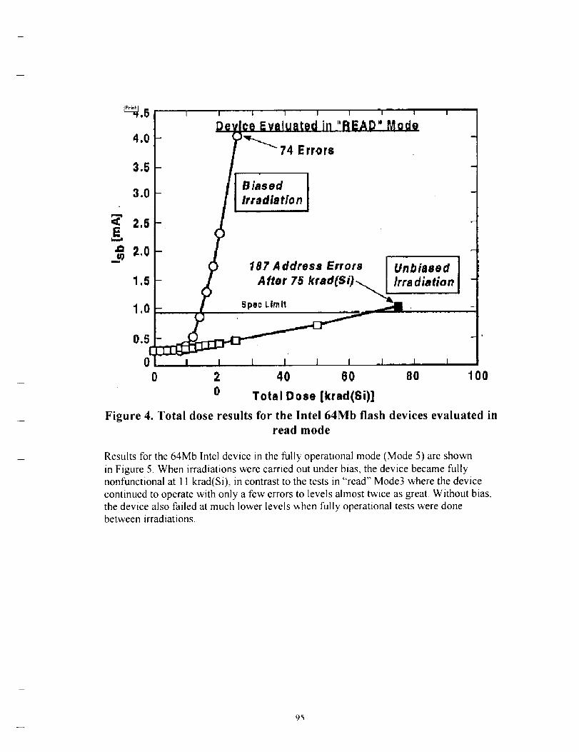
I I t 1 I
4,0
3.5-
3.0-
2,5-
2,0-
1,5-
1,0-
0.5
74 Errors
BiasedIrradia rio n
187 Address ErrorsAfter 75 kraal,
SpmcLimit
Unbiased ]lrra dia rio n
0 I I I
0 2 40 60 80 100
0 Total Dose [krad(Si)]
Figure 4. Total dose results for the [ntel 64Mb flash devices evaluated in
read mode
Results for the 64Mb Intel device in the fully operational mode (Mode 5) are shown
in Figure 5. When irradiations were carried out under bias, the device became fully
nonfunctional at 11 krad(Si), in contrast to the tests in "read" Mode3 where the device
continued to operate with only a few errors to levels almost twice as great. Without bias,
the device also failed at much lower levels when fully operational tests were donebetween irradiations.
95

0,6
0,5
0.4
_0.3
0.2
i).1
00
I I I
.FUnblesed- /IrradJalion / i -
Biased Nonfunctional t ,___.,__Irradiation "' o"'" ""e' _ /
- (static) ;'""'"'_ F 956'Write
L, _ _ ¢ _ 773 Wrfte
F Nonel 3 Write .... t_- errors Intel 64 M b I
/ Flash memory I/ i _ I I i I i
10 20 30 40
Total Dose [krad{Si)]
Figure 5. Total dose test results for the lntel 64Mb flash memory
evaluated in full functional mode
Test results for 128 Mb Samsung devices in the "read" mode are shown in Figure 6.
Without biased irradiation, the standby current increased by several order of magnitude at
about 20 krad(Si). When tested without bias the device functioned to levels above 100
krad(Si) with only a small number of"read" errors.
96

O,B
0.S
-- m,,.' ''[ i I ---_ 1 i
(Devl(;a Evaluated In "READ', Mode
IBiased ]I Irrad iatlon J
~1000 ReadErrors
f f to 13 f
Read Errors \ _
k
o.2- u.b,..d I J J• Irradiation [ _ One Cell Flipped I
"°°°°10 ............................... §_ggL]r_ff....
0 20 40 80 80 100 120 140
Total Dose [krad (81)]
Figure 6. Total dose results for the 128Mb Samsung flash device, tested in
read mode
In studies with full functionality tests erase-mode (Mode 5) failures were observed at
around 8 krad(Si) under bias irradiation as shown in Figure 7. When fully functional tests
were done on devices that were unbiased during irradiation, erase failures occurred at 45
krad(Si)
97

40Failed to erase 511 blocks .---__.__,.
3O
J_2O
10
One cell flipped
Failed to erase 1024 blocks, me
BiasIrradiation
(static)
UnbiasedIrradiation
0 I ..... I_
0 10 20 30 40 50
Total Dose [krad(Sl)]
Figure 7. Total dose test results for the 128 Mb Samsung flash memory evaluated in
Erase/Write/Read mode (Mode 5).
II!. CONCLUSION
Designing systems to effectively use flash memory while avoiding radiation problems,
including destructive effects, is becoming more difficult as the devices are scaled to
smaller feature sizes and larger overall arrays size. Charge pump degradation continues to
be the most significant degradation mode, even for more advanced flash memories.
Microdose effects, although they affecting only a small number of bits, may be on the
verge of becoming a serious problem as transistor sizes scale and manufactures pushtoward the next step in multi-level flash memory designs.
98

REFERENCES
Ill
[21
I31
[41
151
P Pavan, R Bcz P Olivo, and E. Zanom, "Flash MemoD' Cells- An ()vervie\_',
Proceeding of the IEEF. vol 85_ p 1248. (1997)
I1 R Schwartz, D K Nichols and A tt Johnston, "Single-Evenl IJpsel in Flash
Memotries.' IEEEl'rans Nucl Sci.. vol 44, p 2315 (1977)
D N Nguyen, S M Guertin, G M Swift and A. H Johnston. "Radiation Effects onAdvanced Flash Memories," IEEE Trans Nucl Sci, vol.46, p 1744 (1999)
A Baker, R Alexis, S Bell. V Dalvi, R Durante, E Bauer. M Fandrich, O
Jungroth, J Kreifels. M Lansgraf, K. Lee, H. Pon, M Rashid, R Rozman, J. Tsang
K. underwood and C Yarigadda," A 33 V 16 Mb Flash Memory with Advanced
Write Operation," Digest of Papers from the 1994 international Solid-state ircuits
Conference, pp 146-147
D N Nguyen, C I l.ee and A H Johnston,"Total Ionizing Dose Effects on FlashMemories," 1998 IEEE Radiation Effects Data Workshop Record, P 100
99

•- . '/" . ./j , .
7p);
An FPGA-Based Test-bed for Reliability andEndurance Characterization of Non-Volatile
Memory
) * *Vikiam Rao. Jagdish I atel , Janak Patel. and Jeffre). Namkung
Coordinated Science Laborato D, 1308 W Main St, Urbana, I1.61801
Departmenl of Electrical and Computer Engineering, [ lniversib of Illinois al
[ lrbana-Champaign
• Jel Propulsion l,aboratory, 4800 Oak Groove Dr Pasadena. CA 91109
Memory Technology Background:
Memory technologies are divided into two categories The first
category nonvolatile memories, are traditionally used in read-only or read-
mostly applications because of limited write endurance and slov, write
speed. These memories are derivatives of ROM technology, which includesEPROM, EEPROM, Flash, and more recent Ferroelectric non-volatile
memory technology Nonvolatile memories are able to retain data in the
absence of power The second category, volatile memories, are RAM-
devices including SRAM and DRAM Writing to these memories is fast and
write endurance is unlimited, so they are most often used to store data that
change frequently, but they cannot store data in the absence of power Non-
volatile mernory technologies with better future potential are FRAM,
Chalcogenide, GMRAM, Tunneling MRAM and SONOS EEPROM
FRAM is a uses a ferroelectric capacitor to store the data. This
storage mechanism is quite different from that of other non-volatile
memories, that use floating gate technology where the charge is stored Theferroelectric effect is the ability of a material to store a state of electric
polarization in the absence of an applied electric field. An FRAM memory
cell is created by depositing a film of ferroelectric material in crystal form
between two electrode plates to form a capacitor very similar to a DRAM
capacitor FRAM cell could be one transistor one capacitor (IT1C) or a
more robust design using two transistors two capacitors (2T2C) for better
thult tolerance (complementary storing). However, rather than storing data
as a charge on the capacitor, a ferroelectric memory stores data within a
crystalline structure known as Perovskite The Perovskite crystals maintain
two stable polarization states resulting from the alignment of internal
dipoles, which are used to represent '1' and '0' states. Since no external
electric field is required for the ferroelectric material to remain its
polarization, a ferroelectric memory device can retain data in the absence of
power
EEPROM (electrically erasable programmable read-only memory)use memory cells with transistors that are very similar to normal MOS
I0()
transistors, but the transistors have a second, floating gate Applying a
programming voltage VPP (usually greater than 12 V) to the drain of the n-channel EFPROM transisto_ programs the EEPROM cell A high electric
field causes electrons flowing toward the drain to move so last the)' "jump"
across the insulating gate oxide where they are trapped on the bottom.
floating, gate The energetic electrons are referred to as hot and the effect is
known as hot-electron injection or avalanche injection EEPROM
technology is sometimes called _floating-gate avalanche M()S '_ ( FAMOS )
Electrons trapped on the floating gate raise the threshold voltage of the n-
channel EEPROM Once programmed an n-channel EEPROM deviceremains off even with a logic high applied to the top gate An un-
programmed n-channel device will turn on as normal with a logic high top-
gate voltage The programming voltage is applied either from a special
programming box or by using on-chip charge pumps In programming anEEPROM, an electric field is used to remove electrons from the floating gate
of a programmed transistor This is in contrast to EPROMs, which must be
exposed to a UV-lamp to remove electrons from the floating gate This
usually requires the removal of the EPROM from the system
Reliability Issues of FRAM
The major non-fabrication-related issues of FRAM reliability includedata retention, fatigue, aging, imprint, and radiation. Data retention, one of
the most important characteristics of non-volatile memories, is defined as the
ability of a memory to maintain stored data between the time it is writtenand the time it is subsequently read. Although data retention is influenced at
a fundamental level by design and manufacturing factors, retention failures
are accelerated by high temperatures, which cause thermal depolarization ofthe poled state in the ferroelectric material The signal loss due to dataretention thilures recovers after a rewrite and immediate read.
Fatigue occurs in ferroelectric materials with an increased number of
switching cycles (read or write cycles) and is characterized by a decrease in
switchable polarization. This process is related to the electrode interfacial
areas of the memory cells and electric-field assisted migration of oxygenvacancies within ferroelectric materials.
Aging is similar to retention failure in that it is characterized by
signal loss over time, but, unlike retention failures, failures due to aging
occur during the retention period and do not recover after a rewrite and
immediate read. During the aging process, a gradual stabilization of thedomain structure occurs, which causes the ferroelectric material to become
less responsive to applied electric fields.
Imprint is a reliability issue specific to ferroelectric material.
Accumulation of charge in the ferroelectric cell over time make a capacitor
1()1

that has spent a significant amount m one polarity reluctant to s\vitch
polarities
The radiation tolerance of ferroelectric memor_ is limited by the
CMOS circuit elements Prior studies have shown no significant difference
between the radiation tolerance of commercial memo_ _ devices with and
without ferroelectric material
Reliability Issues of EEPROM
The reliability issues with EEPROM are very similar with the
exception of imprint, which is specific to FRAM In addition, the process by
which fatigue occurs differs, and charge-trapping is an aspect specific to
EEPROMs During programming, the control gate of an EEPROM cell is
made positive relative to the source-drain area The floating gate is
capacitatively coupled to the control gate, and when sufficient voltage is
generated and the tunneling threshold is exceeded, electrons tunnel throughthe thin "tunnel" oxide window into the floating gate The negative charge
then remains trapped in the floating gate since inadequate voltage exists.
normally to allow the electrons to tunnel back out. To erase the memory cell,
the process is simply reversed To read the cell, the control gate and source
are brought to predetermined reference voltages and the current through thecells is measured. The transistor of a programmed cell is "on" and thetransistor of an erased cell is "off".
Two basic types of failure occur when EEPROM cell are repeatedly
written and erased: dielectric failure and charge trapping Dielectric failures
are the source of very low level random failures. They are caused by leakage
through minor unscreenable flaws in the tunnel oxide. On contemporary
production EEPROMs, dielectric failures are typically too rare to be noticed
by standard lot sampling techniques until several hundred thousand write-
erase cycles have passed. After this, they create a very low but visible levelof random bit failures
Charge trapping is the effect that creates intrinsic failure inEEPROMs During write-erase cycling, small amounts of isolated negative
and positive charge become trapped in imperfections in the tunnel oxide.
Once trapped, the charge is no longer free to tunnel out of the oxide. In
practice, electrons are more commonly trapped, and their presence creates a
barrier to the tunneling of other electrons through the tunnel oxide. The
apparent voltage needed to tunnel in either direction through the oxideincreases. This reduces the amount of charge that can be moved in and out of
the floating gate. When the accumulation of trapped charge becomes severe
enough, it is no longer possible to move enough charge to clearly distinguisha one from a zero. At this point, the memory cells affected must be
abandoned.
102

It ,s desirable to be able to program EEPR()Ms as quickl 5 as
possible I lowever_ accelerating the programming of EEPROM cells
requires the use of higher programming voltages, which accelerate the
charge trapping mechanism and general b degrade the endurance of theEEPROM
ll might seem intuitive that tunnel oxide might degrade with
endurance cycling and that data retention would suffer as a result But the
effecl of cycling on the retention characteristics of EEPROM memory is
very slight l'hat does occur is not due to increasing leakage through normaltunnel oxide, but the statistical influence of the random failures which are in
fact caused by leakage through rarefied defects The effect of cycling on the
retention characteristics of before reaching the intrinsic limit of EEPROM
memories is so slight, in tact, that it is usually ignored
Tester Design
A custom memory tester was designed to create a low-cost, user-
customizable testing fbr non-volatile memory that could perform reliability
and endurance tests. The objective was to evaluate the reliability and
endurance characteristics of various non-volatile memories for potential use
in space applications
A XII,INX XC4010E 10,000 gate, 5V FPGA was chosen tbr the 5Vmemories, and a XII,INX XC4010XL, a 3.3V version of the XC4010E, was
chosen/br the 3.3V memories. The tester board contains a parallel port tbr
communication with a PC, an LED for error readout, and an EEPROM
socket for PC-independent operation
The tester can be configured to perform reliability or endurance tests,
and each test can log errors in one of two ways. The error data can either be
logged on a PC through the parallel port, or the tester can be used by itself,
independent of a PC, by using an EEPROM to load the bit stream file and
"scrolling" the error information on a 7-segment LED display The memory
tester configuration for a parallel FRAM is shown below
This test bench offers several advantages over commercial testers
when used/'or reliability and endurance testing. Endurance testing to a chip'sspecifications could involve more than 10l° read/write cycles, which can
take up to 28 days for the Ramtron FM24C04 serial FRAM Commercially
available memory testers with high hourly rates may prove extremelyexpensive for testing NVMs with 1012 to 1015 read/write cycles. In
comparison, the FPGA-based testers are inexpensive and more flexible. Ifseveral FPGA boards are used, many chips can be tested simultaneously at a
fraction of the cost compared to the commercial testers. The highly portable,
PC-independent nature of the test bench would also make it suitable for use
in radiation testing, given proper shielding for the tester
103
PARALLEL
PORT
EEPROM
SOCKETRAM FPGA CONTROL
YT_
Figure 1: Non-volatile memory tester
ERROR
DISPLAY
Test Methodology
A MATS+ test was chosen to test the reliability of the non-volatile
memories. In order to understand the test procedure, a brief example and
explanation of Van de Goor's memory test notation is provided below:
UP(W]0101010; R; W0101OI0])
UP - Perform the entire set of operations
from the first memory address to the last
WI0101010 = Write the data pattern _I0101010'
R Read back the data
W01010101 Write the data pattern 0]010]0]
(Increment address and loop)
in parentheses
The MATS+ reliability test can detect address decoder faults and stuck-at
faults, and was programmed to cycle through all the addresses in thememory. This reliability test was chosen because it met the minimum test
criteria while fitting into the relatively small FPGA Again using Van de
Goor's notation, the MATS+ test is described as follows:
UP (W01010101)
:P(R; WI0101010)
DOWN(R; W01010101)
LOOP BACK TO
In order to test the endurance of the non-volatile memories, the
following basic endurance test was used:
. (W01010101; R; Wl0101010; R)
LOOP BACK TO (I)
1()4
Due to the prohibitive amount of time required to exhaust alladdresses in the memories with an endurance test, it was decided that a
single address or small range of addresses would be used instead.
Upon an error in during either test, the tester logs the total number oferrors that have occurred, the number of read and write cycles at the point
the error occurred, the memory address at which error occurred, the incorrect
data value read, and (on the reliability test) it indicates the part of the
memory test the failure occurred on. If the parallel port version of the tester
is used, a simple program logs the data on the screen and gives the user the
option of saving the data to a file. The other version of the tester, which isindependent of the PC, scrolls the error information corresponding to the
most recent error across the LED display, using various symbols to describe
the data about to be displayed. An EEPROM is used in this tester so that a
PC is not required to download the FPGA bit stream, which makes it
completely independent of the PC.
Test Procedure and Preliminary Results
Memory testing is ongoing, and the results to date are preliminary.Three non-volatile memories are under test: Ramtron FM24C04 serial
FRAM, Ramtron FMI808 Parallel FRAM, and the Northrop-Grumman's
256 kb Rad-ttard EEPROM Reliability tests have produced no errors in any
of the memories Endurance testing on the Ramtron FM24C04 serial FRAM
has exceeded the endurance specification of the chip (I.0xl0 _° read write
cycles) by over four times (it has undergone 4.2x10 I° read/write cycles) with
no errors. Endurance testing on the Ramtron FM1808 parallel FRAM has
not yet exceeded the endurance specifications, but no errors have surfaced todate.
Ramtron
Serial FRAM
RamtronParallel FRAM
NG EEPROM
Status
Testbed
complete:Both tests
runningTestbed
partiallycomplete:endurance
tests runningTestbed work
in progress
# R/W Cycles(Endurance)
4.2E10
.6E10
N/A
Endurance
Spec
1E10
1E10
10,000
Table I: Preliminary Results
Full test results will be available by December, 2001.
I o5

Concluding remarks
A custom memory tester was designed to create a low-cost, user-
customizable testing fbr non-volatile memory that could perform reliabilityand endurance tests. The tester board contains a parallel port for
communication with a PC, an I,ED for error readout, and an EEPROM
socket for PC-independent operation. The main objective is to evaluate the
reliability and endurance characteristics of various non-volatile memories
for potential use in space applications Testing is currently in progress for
various memory chips. Results are expected l-brm various tests in next twomonths.
Acknowledgments
Research described in this paper, was carried out at the Jet
Propulsion Laboratory, California Institute of Technology, and was
sponsored by the National Aeronautics and Space Administration's
Electronics Parts and Packaging Program (NASA/NEPP). The authors
acknowledge the help received from Dr. Charles Barnes and Mr Choon Lee.The authors are grateful to Mr. Michael Fitzpatrick of the Northrop
Grumman for the samples of EEPROM parts.
References
[1 ]. Ramtron Application Note: FRAM Technology Backgrounder
[2]. T. Hadnagy, et al., "Retention After Fatigue of Ferroelectric Memories"
http://www.ramtron.com/products/techpaperlibrarg/Reten& Fatigue
Domokos.pdf
[3]. A Sharma and Alexander Teverovsky, "Preliminary Evaluation of DataRetention: Characteristics for Ferroelectric Random Access Memories
(FRAMs)", NASA Goddard Space Flight Center, pp I-4
[4]. A. J. Van de Goor. "Testing Semiconductor Memories'John Wiley &
Sons, Inc.
106

SESSION #3: ProcessingWednesday, November 7,2001
4:20 PM - 5:30 PM
Chair: M. White, Lehigh University
4:20 PM
4:40 PM
5:00 PM
Copper/low-k interconnect integration into 0.15 _tm single poly
EEPROM technology; V. Shekhar, I. Rahim, C. Sardana, and
G. Thalapaneni, Altera Corporation, C. Lin, M. Ho, Y Wang,
and D. Kuo, Taiwan Semiconductors Manufacturing Company
Process Optimization for MOCVD of SrBiJa:Q for Non-Volatile
Memory Applications; D. Burgess, Aixtron Incorporated
Atomic Scale Structure of Giant Magnetoresistive Multilayers:
Energetic Adatom and Surfactant Effects; X. Zhou, W. Zou,
R. Johnson, and H. Wadley, University of Virginia
107
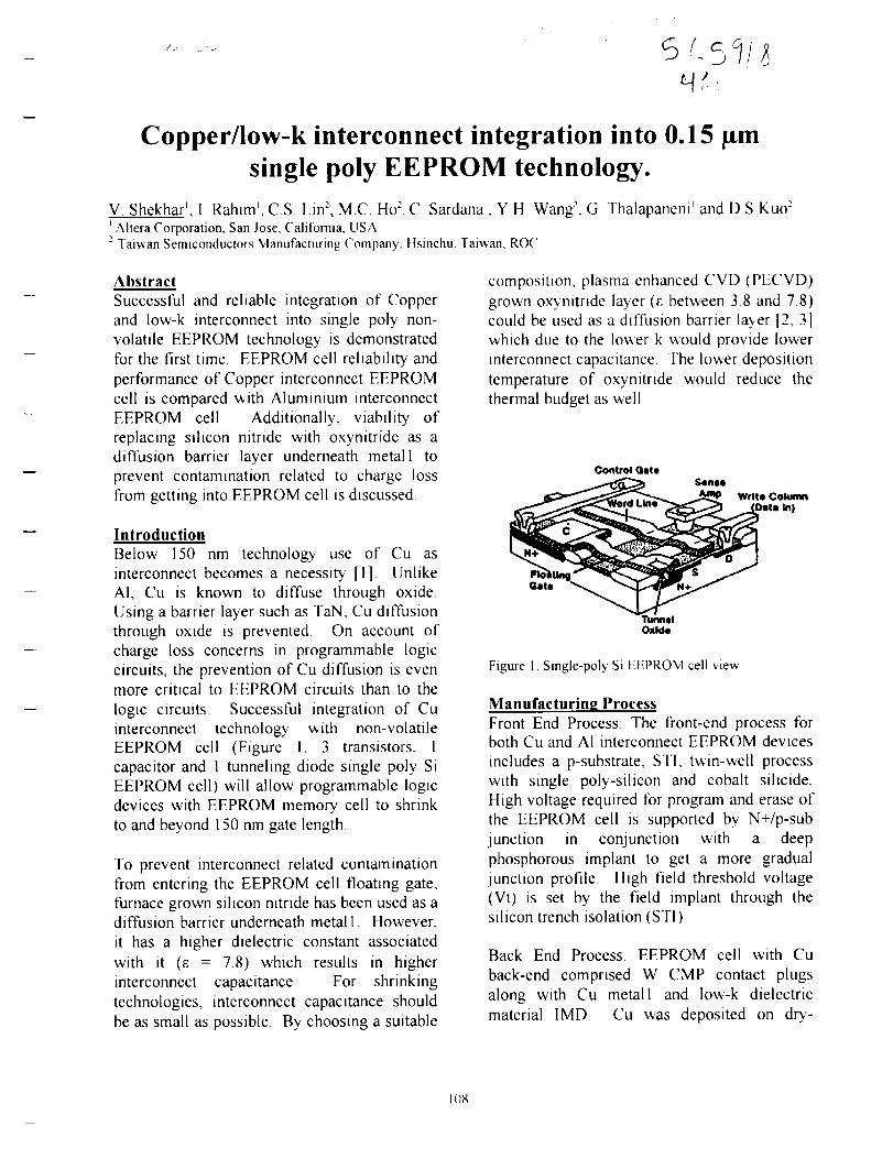
Copper/iow-k interconnect integration into 0.15 lttm
single poly EEPROM technology.
V. Shekhar', I Rahim', C.S IAn e, M.C. Ho e, C Sardana _, Y H Wang:, G Thalapaneni _and DS Kuo:I/\ltera Corporation, San Jose, California, USA
-_Taiwan Semiconductors Manufacturing Company, tlsinchu. Taiwan, RO('
Abstract
Successful and reliable integration of Copper
and Iow-k interconnect into single poly non-
volatile EEPROM technology is demonstrated
for the first time. EEPROM cell reliability and
performance of Copper interconnect EEPROM
cell is compared with Aluminium interconnect
EEPROM cell. Additionally, viability of
replacing silicon nitride with oxynitride as a
diffusion barrier layer underneath metal l to
prevent contamination related to charge loss
from getting into EEPROM cell is discussed.
Introduction
Below 150 nm technology use of Cu as
interconnect becomes a necessity [I], UnlikeAI, Cu is known to diffuse through oxide,
Using a barrier layer such as TaN, Cu diffusion
through oxide is prevented On account of
charge loss concerns in programmable logic
circuits, the prevention of Cu diffusion is evenmore critical to EEPROM circuits than to the
logic circuits Successful integration of Cu
interconnect technology with non-volatile
EEPROM cell (Figure I: 3 transistors, 1
capacitor and 1 tunneling diode single poly Si
EEPROM cell) will allow programmable logic
devices with EEPROM memory cell to shrink
to and beyond 150 nm gate length.
To prevent interconnect related contamination
from entering the EEPROM cell floating gate,
furnace grown silicon nitride has been used as adiffusion barrier underneath metal l. However,
it has a higher dielectric constant associated
with it (_ = 7.8) which results in higher
interconnect capacitance. For shrinking
technologies, interconnect capacitance should
be as small as possible. By choosing a suitable
composition, plasma enhanced CVD (PECVD)
grown oxynitride layer (c between 3.8 and 78)could be used as a diffusion barrier layer [2, 3]
which due to the lower k would provide lower
interconnect capacitance. The lower deposition
temperature of oxynitride would reduce the
thermal budget as well
Controt Gste
Senso
w,,,.,,,,,;,,,
P
Tunne!Oxide
Figure 1. Single-poly Si EI:,PROM cell view'
Manufacturinlz Process
Front End Process: The front-end process forboth Cu and AI interconnect EEPROM devices
includes a p-substrate, STI, twin-well process
with single poly-silicon and cobalt silicide.
High voltage required for program and erase of
the EEPROM cell is supported by N+/p-sub
junction in conjunction with a deep
phosphorous implant to get a more gradual
junction profile High field threshold voltage
(Vt) is set by the field implant through the
silicon trench isolation (STI).
Back End Process: EEPROM cell with Cu
back-end comprised W CMP contact plugs
along with Cu metal l and Iow-k dielectric
material IMD Cu was deposited on dry-
t()8

etched oxide trenches (single damascene) using
a combination of sputtering (TaN liner/Cu
seed) and electro-chemical plating (ECP) The
Cu film was subsequently planarized with CMP
followed by nitride passivation The AI test
chip comprised W CMP contacts and via plugswith a FiN/AICu/TiN liner stack and SiO2 ILD
Splits for silicon nitride (furnace grown) and
oxynitride blanket layer (PECVD-grown using
Sill4 ÷ N20 constituenl gases) underneathmetal l was used with AI back-end wafers to
compare the effecl of these layers as a diffusion
barrier layer for unwanted species A brief
process flo,a is shown in "Fable I
]'ABI.E 1 Process Flow
Logic {(7ore)OD/STI
Twin-well
Field hnplanl
Gate Poly
EEPROM Module
{additional steps to the Logic steps)
N 4 imp under Tunnel Windo_
Tunnel Oxide
Deep P Implant at HV S/D
LDD Imp for all devices
Spacer FormationNMOS S/D
PMOS S/D
Diffusion Barriel Layer
Contact and Metallization
Experimental Results and Discussions:Characterization of EEPROM cells with AI and
Cu interconnects as well as silicon nitride and
oxynitride diffusion barrier layers were
pedbrmed for reliability and perfbrmance, The
erase and program cycling for the EEPROM
cell is done through a Fowler-Nordheim (F-N)
tunneling mechanism Erase and program
verification is done through the read path
Reliability and performance comparison ofEEPROM cells with AI and Cu interconnects
Performance comparison of EEPROM cells
with both types of interconnects was done by
taking erase Vt versus erase time and lcell
versus program time measurements in figure 2
and figure 3 respectively Icell is the current
through the sense amp when EEPROM cell is
programmed (electrons are tunneled back into
the substrate) and word line is high (figure I).
According to the graph in figure 2, after 1000ms of erase time, the difference in Vt between
the AI and Cu interconnects EEPROM cells is
less than 1% According to the graph in figure
3, after 100 ms of program time, difference inIcell between the AI and Cu interconnect
EEPROM cells is less than 1% The graphs in
figure 2 and 3 reflect, as expected, that
performance of EEPROM cells with A1 and Cuinterconnects is almost the same
55
ab
m
35
3
2s|
?
" ]u
+ A
. . ...,++'_.. : , "f
-L__ . •. +7
{32 ?4 06 08 12
T:me (See)
Figure 2: Erased VI versus erase time graph for single bit
EEPROM cells with Cu and AI interconnects.
270
0 001 002 003 004 005 006 007 008 009 O" 011
TiltMI (81_)
Figure 3: lcell versus program time graph for single bit
EEPROM cells with Cu and AI interconnects•
109

l)ata Retention: Water level bake was done on
both wafbrs with AI and Cu backend The
following procedure was adopted for the data
retention test (1) program/erase cycling (2)
erase margin Vt (3) bake at 125 °C (4) erase
margin Vt Step 3 followed by step 4 was
repealed for differen! bake times
l:tase margin after 500 hours bake time at 125°C shd'ted less than 15% for the EEPROM cell
with Cu interconnecl This is comparable to
the erase margin shift under the same bakeconditions for the identical EEPROM cell with
AI interconnect The graph in figure 4 plotserase Vt versus bake time for both AI and Cu
interconnect EEPROM cells. This
demonstrates that Cu interconnect technology
can be integrated reliably with the non-volatileEEPROM cell
0 100 200 300 400 500 600
Bake Time (Hour_l)
Figure 4: Graph showing erase margin versus bake timefor single poly EEPROM cell with AI and Cuinterconnect,
Reliability comparison of EEPROM cells with
silicon nitride and oxynitride barrier layers.
Furnace grown silicon nitride was used as a
diffusion barrier layer to prevent contamination
from reaching the floating gate of the non-
volatile cell Oxynitrides as barrier layers have
received an increasing amount of interest due to
the possibili_ that. by choosing the proper
compositioa the excellent electricalcharacteristics of SiO: and the barrier
properties against moisture and other sources of
contamination of silicon nitride may be
preserved [2] Additionally, oxynitrides
deposited b} PECVD at lox_ temperature \_ould
be a bette_ choice than furnace-deposited
silicon nitride at higher temperature for
shrinking technologies due to smaller thermal
budget of the former [4-6]
Data Retention. Wafer level bake at 125 °C was
done on both wafers with identical EEPROM
cells but different diffusion barrier layers of
nitride and oxynitride The same procedure
described earlier in this paper was used for the
data retention test The graph in figure 5 shows
erase margin versus erase bake time after 500hours of bake at 125 C for both EEPROM cells
Erase margin shift for EEPROM cell with
oxynitride as diffusion barrier blanket layerwas more than 12% while that fbr EEPROM
cell with silicon nitride as a diffusion barrier
blanket layer was less than 15%. However,
there was no erase Vt margin shift from 168hours to 500 hours. On account of shift in the
Vt margin from zero hour to 168 hours, it is
concluded that plasma enhanced oxynitride is
an unsuitable choice for diffusion barrier layer.
The possible cause of erase Vt margin shift
from zero hour erase margin to 168 hours
might not be due to real charge flow from the
floating gate but could be as a result of charges
in the oxynitride layer that couple voltage to
the floating gate thereby shifting the margin.
Charges in the oxynitride layer deposited byPECVD could arise from the creation of
dangling bonds (DB) which are enhanced as
more O atoms are incorporated in the
oxynitride film. However, the formation
mechanism of defects in oxynitride films with
different compositions is unclear [7]. Also,
conventional plasma-assisted CVD with Sill4
ll(_

as silicon sourceintroduceshydrogenin thedepositedfilms that causesthermalinstabilityof physical and electrical propertiesduringsubsequentprocessing[2, 8] D. R Coteandco-authors[9] have suggestedthat PECVDoxynitride film with higherrefractiveindex1.80to 185 mightbemoredesirablelbr barrierapplication The bondingstructural analysesand electrical measurementson PECVDoxynitride films done by these authors haveshown that films with refractive indices of 1.75
to 1.80 have low surface states with minimal
leakage
5 ! .............
51
4
g
200 400 600 800 1000
Bake Time (Nour)
Figure 5: Graph showing erase margin versus bake timecomparison for EEPROM cell with silicon nitride andoxynitirde as diffusion barrier layers underneath AImetal I.
Conclusions
The experimental results show that Cu/Iow-kinterconnect can be used as an interconnect of
choice with non-volatile EEPROM devices
without causing significant reliability and
performance concerns Experimental results
also indicate that PECVD oxynitride may not
be a good substitute for furnace grown silicon
nitride presently used as a diffusion barrier
layer underneath metal l in the EEPROM cell
due to increased charge loss possibly, caused by
the creation of dangling bonds and charge
states in PECVD oxynitride.
Acknowledgments
The authors v_'ould like to thank Myron Wong
and Brad Vest from Altera design engineering
for their valuable inputs related to the cell
design as well as Samit Sengupta from Altera
technology' engineering for inputs related to Cu
structures design Authors would also like to
thank TSMC lab and processing R&D groups
for manufacturing and providing the wafers in a
timely manner
References
[1] International Technology Roadmap forSemiconductors, 1999, p-167
[21 O. Sanchcz, J. M. Martinez-Duart, R. J. Gomez-Sanroman, R Perez-Cascro, J of Mat. Sci 34 (1997)3007-3012
[3] E.P Gusev. H.-C I.u, E I.Garfunkel, "[.Gustafsson,Ml..Green, IBM J.Res. Dev VOI,. 43 No.3 May 1999[4] B. ttajji, P. Temple-Boyer, F. Olivie, A. MartinezThin Solid Films (1999) vol. 354, no. I-2, p 9-12[5] D R Harding, L.U.T. Ogbuji, M. J Freeman, J.Appl. Phys. 78 (1995) 1673
[6] O. Sanchez, M A Aguilar, C Falcony, J.M.Martinez-Duart, J. M. Albella, J. Vac. Sci. Technol. A14(1996) 2088.[7] S. Hasegawa, S. Sakamori, M. Futatsudera, T.Inokuma and Y. Kurata J Appl. Phys vol 89 number 5 P2598[8] R C. Sun, J. T. Clements, J. J. Nelson, 18th AnnualProc. Reliability Phys (IEEE, Las Vegas, 1980) P. 244.
[9] D R. Cote, S V Ng, A K. Stamper, D S. Armbrust,D. Tobben, R. A. Conti, G Y Lee, IBM J. Res. Dev. Vol43 No. 12 Jan/Mar 1999
111

Process Optimization for MOCVD of SrBizTa20,_ tbr Non-Volatile MemoD Applications
Presenter: D Burgess, Aixtron
Material for this presentation was not available at the time of publication
112

Atomic Scale Structure of Giant Magnetoresistive
Multilayers: Energetic Adatom and Surfactant Effects
X. W Zhou (Xz8n@virginiaedu). W Zou. R A Johnson, H N G. Wadley
Department of Materials Science and Engineering, School of Engineering and Applied Science, University
ot Virginia, Charlottesville, VA 22903, US A
Abstract--The deposition ol higher quality giant
magnetoresistive (GMR) metal multilayers is essential fo[
improving the performance of magnetic field sensors and
nonvolatile random access memories. Improved
performance requires reduction of both the atomic scale
interracial roughness and interlayer mixing in the as
deposited films. The first step is to develop relationships
between controllable process parameters and the atomic
scale interracial composition/structure. We have used
atomistic simulation and controlled experiments to begin
to address this issue. We show that control of the adatom
energy and the use of a silver surfactant can improve the
interface structurc of multilayers Increasing the adatom
energy causes surface flattening due to enhanced surface
reconstruction, but results in interlayer mixing due to
impact induced atomic exchanges. A modulated energy
deposition scheme was found to reduce both roughness
and mixing The addition of a small quantity of silver was
found to reduce the activation barriers for surface atomic
assembly and to enable the assembly process kinetics to
be shifted to a regime where conventional deposition
processes are able to create high quality interfaces.
TABI.E OF CONTENTS
1 INTRODUCTION
2 ATOMISTIC SIMULATION METHODS
3. EFFECTS OF HYPERTHERMAI. ENERGY
DEPOSITION
4. tlYPERTHERMAL ENERGY IMPACT
MECHANISMS
5, IMPROVED DEPOSITION PROCESS
6 SURFACTANT EFFECTS
7 SURFACTANT MECHANISM
8. CONCLUSIONS
9, ACKNOWLEDGMENTS
1. INTRODUCTION
In 1988, Baibich et al discovered that nanoscale Fe/Cr/Fe
multilayers exhibit a very large drop in electrical
resistance when a moderate magnetic field was applied I_l
Since then, many other multilayer systems composed of
(_50A thick) ferromagnetic metal layers separated by
(~20A thick) nonferromagnetic conductive metal layers
have been found to possess this giant magnetoresistivc
(GMR) property. The most frequently studied systems
have either a Co/Cu/Co I-_'31ol a NiFe(Co)/Cu/NiFet Co) 14:1
repeated unit. These GMR materials are well suited for
sensing small magnetic fields. Intensive research has
quickly resulted in the development of sensors for thereadheads of hard disk drives. This contributed to thc ver'_
large recent increases in the hard drive storage capacity M.
Many groups are now also exploring the application ol
these materials to create nonvolatile magnetic random
access memot3.' (MRAM)I_l
Both the readhead sensors and MRAM applications of
GMR materials are greatly improved if better GMR
properties can be achieved. Relevant GMR properties
include a high GMR ratio (defined as the maximum
resistance change divided by the resistance at magnetic
saturation), a low magnetic saturation field, a high
thermal stability, minimal coercivity, and weak
temperature dependence. However, efforts to develop a
deposition process that can reliably produce a superior
combination of these properties have been prolonged
because many deposition conditions sensitively affect the
atomic scale structure of the multilayers which in turn
control GMR properties
When pairs of ferromagnetic layers are separated by an
appropriate thickness, the RKKY interaction causes their
magnetic moments to align antiferromagnetieally in a
zero magnetic field FI. Spin dependent electron scattering
then results in a relatively high electrical resistance 18.,_1.If
an external magnetic field is applied to align the magnetic
moments of the ferromagnetic layers, the spin-dependent
electron scattering is reduced, and so is the electrical
resistance of the film. Experiments indicated that a
significant change of the GMR ratio could occur when the
spacing between the ferromagnetic layers is varied by as
little as 2 A t-_l. In mtfltilayers with rough interfaces, Neel
coupling occurs which greatly increases the coercivity of
the device. This becomes increasingly significant as the
roughness amplitude and wavelength approach the layer
spacing. Alloying (mixing) of one layer with the atoms of
113

anothercausesan increasein spin independentscatteringI_1anda lossor localmagneticalignmentI>1whichalsoreducethesizeor theGMReffect.HighqualityGMRmultilayersmustthereforehaveapreciselycontrolledlayerthickness,verylowinterracialroughnessandminimalinterlayermixing.Thedevelopmentofprocessesthat resultin relativelysmooth,unmixedinterfacesiscriticalif the(;MRratiosof multilayersaretobcincreasedI_l
t:xperimcntsprovidccluestoidentif:_the key processing
parameters sensitive to GMR properties Similar
architectur_ (-}MR multilayers have been synthesized b}
ambicnt temperature sputtering lal, ion beam deposition It:l.
and molecular beam epitaxy (M BE)Ill The reported GMR
ratio fo) ('o,"('u(~20A)/Co multila_'ers deposited usingthese different deposition methods [L I are shown in Fig. 1.
In the MBE case the GMR ratio data was measured at 4.2
K Parkin et al have measured the GMR ratio of the
[Co(10A/Cu(93A)]t_, multilayers as a function oftemperature 171.Their experiments indicated that the room
temperature GMR ratio is about 63% that at 4.2 K, so in
Fig 1 wc have converted the low temperature MBE data
to room temperature by multiplying a factor of 63% Fig. 1
indicates that multilayers deposited using low-pressure
magnetron sputtering and ion beam deposition (IBD) are
generally superior to those produced using MBE. This is
somewhat surprising considering that the GMR
multilayers were first discovered using MBE {_1 and that
MBE has been so successful to deposit high purity, highly
crystalline semiconductor films. A notable feature of
MBE method is that the energy of its deposition flux is
near thermal equilibrium, which is much lower than the
other sputter deposition methods. The question is if this
low energy contributes to the poor quality of the films,
and why
100.0
80,0
o_ 6o.o
m
2_ 40.0
20.0
0.0
©
°
rf diode/MBE* triode IBD Magnetron
sputtering sputtering
Fig. 1. GMR values reported for different deposition
processes. *MBE data were converted (see text).
1:[14], E:[15], #:[16], O:[17], e:[18], O:
[19], _: [20], ®: [12], _D: [21], +: [29], X: [22],
*: [23], A: [24], A: [3], V: [25], V: [26], =: [2],
,: [7], .,: [27], o: [28]
Kano et al I-",t studied the effects of deposition
temperature on the GMR ratio of the [Co(10A
(-'u( 10A)]>_, multilayers. Their data are shown m Fig. 2. It
indicates that at substratc temperatures above 100"(', the
GMR ratio rapidly decreases as the substrate temperature
is increased. On the other hand, the GMR ratio gradually
increases as substrate temperature is decreased from
100°(" The (]MR ratio is seen to approach a saturated
high value at near room temperature. The results above
appear to indicate that process conditions that promote
thermally activated atomic assembly during deposition arc
not favorable tbt GMR multiplayer growth
8O
70 -/----_
\.
8-.° 60 \" \
50
40
30
[Co(lOA)/Cu(lOA)}.0_
\"\
0 20 40 60 80 1O0 120
Substrate temperature (°C)
Fig. 2 GMR ratio as a function ofsubstrate temperature.
A simple thermodynamics analysis shown in Fig. 3 can
explain some of the observations in Figs 1 and 2.
Consider the growth of an A/B/A multilayer stack.
Suppose that the bond energy between A atoms is higher
than that between B atoms. If atoms A and B are about
the same size, then B can wet A because the more
strongly bonded A atoms can pull B atoms onto their
surface, Fig. 3(a). ttowever, A will then not wet B
because the relatively weakly bonded B atoms cannot
reconstruct A clusters, Fig. 3(b). This indicates that
during the deposition of an A/B/A multilayer system
under thermally equilibrated conditions (i.e. kinetic
conditions that permit the equilibrium structure to be
achieved), the step flow growth mode can only be
achieved at either the A on B or B on A interface but not
both. It should also be noted that even when the bond
strength argument favors the step flow growth mode,
surface roughness could still arise when a large strain
energy exists due to size differences between the differentelements.
In GMR multilayers the surface roughness at completion
of each layer growth sets the roughness of the interface
created by overgrowth with the next metal. This
mechanism is presumed to contribute to the poor GMR
multilayers deposited using MBE as seen in Fig. 1. The
sharp drop of GMR ratio for films deposited at
temperatures above 100"C, Fig 2, can also be a result of
114

significantinterlayermixingductoenhancedinterlayerdiffusion
(a) B atoms wet A surface
g y _---_,
A
surface energies satisfy YB + YAB < YA
(b) A atoms do not wet B surface
B
e defined by YACOS(0) + YAB = _'B
Fig 3. Surface morphology under thermal equilibrium
growth conditions.
The atomic scale structure of multilayers results from
atomic assembly processes active during deposition. This
assembly can be mediated by controlling the temperature
of the surface and the deposition rate which in effect
control the time available for a thermal fluctuation to
induce an atom to hop from one site to another [,0]. Hops
can also be induced by other (nonthermal) processes such
as hyperthermal metal impacts m.,-'l inert gas ionassistance ml, and the heat of reaction when atoms are
condensed on the film ml. The relative success of the
magnetron sputtering and IBD processes reviewed above
suggest that the use of growth conditions that constrain
thermally assisted processes combined with "hot" metal
atoms may be preferred for the growth of GMR
multilayers. Atomistic simulations provide a route to
explore these ideas in detail.
2. ATOMISTIC SIMULATION METHODS
If the atomic scale interfacial structttres are sensitively
affected by the fluxes incident upon a growth surface, it is
important that they be well understood For the low
pressure sputter and IBD processes that can produce good
GMR multilayers, the adatoms can have a wide
distribution of energies with an average in the 5-10 eV
range and a tail extending to above 30 eV 1_41 The adatom
energy can be reduced by increasing the chamber pressure• 1_51
and target to substrate d_stance -. Recent experiments
have also linked strong variations in the GMR ratio to the
existence of secondary inert gas flux incidence upon the
growth surface l a6].
"fo realistically predict the effects of energetic impacts, a
highly prcdictivc atomistic simulation method must bc
used. In our work, a molecular dynamics (MD) approach
is used to simulate the multilayer growth, including the
transition of atoms from vapor to a solid suffacc and the
subsequent surface reconstruction. Because Newton's
equations of motion are used to describe the evolution of
atomic positions, the detailed atomic structures of a
deposited film and many of the mechanisms active during
the deposition can be correctly described provided a high
fidelity interatomic potential is used to calculate the
interatomic forces. We have adapted the embedded atom
method (EAM) potential initially developed by Daw and
Baskes [37] EAM assumes that the total crystal energy is
the sum of a pairwise potential and an energy required to
embed each atom into its local medium with a given
electron density. Because this embedding energy dependson the net local environment of each atom, EAM well
accounts for the many-body effects. EAM models hence
provide a good format for solving problems involving
surfaces and other defect states.
EAM potentials developed for atoms of a single element
cannot generally be applied to model the behavior of
alloys. This arises because the reference states adopted fordifferent elements are often not consistent, and the
analytical forms and cut-off parameters of the interatomic
potentials of individual elements are incompatible.
However, by normalizing the EAM potential I_sl and using
a unified potential cutoff function, we have recently
developed a generalized EAM potential database that
enables calculation of alloys with any combination of
sixteen metals (Cu, Ag, Au. Ni, Pd. Pt, AI. Pb, Fe, Mo.
Ta, W, Mg, Co, Ti, and Zr) i_.40I. These potentials are
well fitted to basic material properties such as lattice
constants, elastic constants, bulk moduli, vacancy
formation energies, sublimation energies, and heats of
solution.
Details of our MD simulation can be found in ref. [41].
Briefly, a computational crystal was created by assigning
atom positions according to lattice sites. Periodic
boundary conditions were used in the lateral x and z
directions to extend the crystal dimensions and a free
boundary condition was used for the vertical y direction.
Atoms with prescribed kinetic energies were randomly
injected (from far above) to the top y surface at a
frequency that gave rise to a desired deposition rate. The
evolution of atom positions (and hence the atomic
structure of the entire system) was then solved from
Newton's equation of motion. To calculate the stress and
account for relaxation of the crystal size under the
influence of the lattice mismatch between different layers,
a Lagrangian form of Newton's equation of motion was[42 I
used . To prevent the crystal shift due to momentum
transfer at the top y surface, the positions of the two
bottom monolayers of the substrate atoms were fixed
during simulation. Isothermal growth is achieved by
applying a temperature control scheme 14_1 to
115

unconstrained part of the substrate crystal+ This regionwas then advanced upwards as deposition progressed in away that left several free mono[ayers at the surface. Thisenabled the effects of energetic impacts to be realisticallysimulated.
3. EFFECTS OF HYPERTHERMAL ENERGY
DEPOSITION
The simulation methodology has been used to analyze thegrowth of a Cn(20A)/Ni(20A) unit as a ftmction of
adatom energy at a fixed normal adatom incident angle, asubstrate temperature of 300 K and a deposition rate of Inm/ns. The detailed atomic structures of the simulated
muhilayers are shown in Fig 4, where Ni and Cu atomsare marked with black and white balls respectively. It canbe seen that at the low incident energies (-0.1 eV or less)typical of either MBE or high pressure sputtering, theinterfaces exhibited both significant roughness and Cu
mixing in the subsequently deposited Ni layer.Interestingly, little mixing of Ni is seen in either of the
copper layers. This phenomenon has recently beenexperimentally observed in the atomic scale structures ofmultilayer stacks E+01
Increasing the incident energy from 0.1 to 5.0 eVsignificantly reduces the roughness of both the Cu-on-Niand the Ni-on-Cu interfaces. The Ni-on-Cu interface isflatter than the Cu-on-Ni interface at low incident
energies, but this difference becomes small when theincident energy increases to 5.0 eV where both interfacesapproach a saturation flatness. Increasing the incidentenergy from 0.1 to 1.0 eV appears to reduce the mixing ofCu in the Ni layer, but the mixing is significantlyincreased as the incident energy is further increased.
Again Cu atoms are dispersed in the subsequentlydeposited Ni layer much more significantly than Ni atomsare dispersed in the subsequently deposited Cu layer.
Both the amplitude and wavelength of interracialroughness are expected to influence the GMR ratio. Anaverage amplitude to wavelength ratio rt was used tocharacterize the roughness of the simulated structures m iThe value of rt as a function of incident energy is plotted
in Fig. 5(a) for both the Cu-on-Ni and the Ni-on-Cuinterfaces. Fig. 5(a) shows that the interfacial roughnessinitially decreases with increasing incident energy,reaches a minimum between about 2.0 and 3.0 eV for theNi-on-Cu interface and at about 4.0 eV for the Cu-on-Ni
interface, and then begins to rise as the incident energy isincreased beyond 4.0 eV.
When surface roughness is experimentally measured sayby atomic force microscopy, the average deviation r_,,of asurface profile from the mean surface height, is usuallyobtained [41 If the surface roughness is sinusoidal, r_,can
be linked to q. The r, surface roughness is also shown (onthe right coordinate) in Fig. 5(a).
o o o o o
T= 300K
normal incidence
-..L " :-_ ..
(a) E =0 leVy[1111_
Ni substrate L__,._""_ _
loA t'z [11o](b) E,= lOeV
i/('c) E, = 50eV
Fig. 4. Simulated multilayer structure as a function ofadatom energy.
Kools u41has experimentally measured the r_, surfaceroughness during the growth of NisuFe_,0/Cu/Ni80Fe_,uexchange-biased spin-valves. His results are included inFig. 5(b). The samples used in Kools' experiments weregrown using magnetron sputtering at a constant target-substrate distance of 109 mm and various chamber Ar
pressures between I and 10 reTort. Using MD predictionsof the energy spectrum of sputtered Cu i34] and a binarycollision model for copper transport in an argonatmosphere i,_l the average incident atom energy wasestimated to be about 0.1 eV at 10 mTorr and about 4.0
eV at I mTorr. These energies and the equivalent
pressures are indicated in Fig. 5. It can be seen that thepredicted decrease of roughness with incident energy inthe low (thermal) energy range, the existence of aminimum roughness in the intermediate energy range, andthe increase of roughness with incident energy in the high(hyperthermal) energy regime all agree well with the
experiments.
116

(a) simulated interracial roughness for sputtered Ni/Cu/Ni
P_r " l()r_T_r Pa = m* r
L
d; 3L
o_2 • ,.,
Or'r
Ni o'_ CJ
%-;. --__. __ __ _J- - ---
f;iJ cjr, %
Incident energy E (eV)
(b) experimental surface roughness for sputtered NiFe/Cu/NiFe*
,2
/
./
n3
&$
5
3
<
1
L,-: I ev L,-4 bev
L'
17 I; ; 4
Pressu_e PA (mTorr)
Fig 5 Interfacial roughness as a function of adatomenergy.
Fig 4 qualitatively indicates that the degree of Cu mixingin the Ni layer is affected by the adatom incident energy.The extent of Cu mixing in the Ni layer can be quantifiedby the probability of finding a Cu atom with many Niatom neighbors. The probability, p, of a Cu atom havingat least eight Ni nearest neighbors was calculated and isshown in Fig. 6(a) as a function of incident energy.Fig6(a) more graphically shows that Cu mixing initiallydecreases with increasing incident energy, reaches aminimum at an energy of 1.0-2.0 eV, and then increasessignificantly with increasing incident energy. Serious Cumixing (p = - 1.7%) occurs when the incident energyapproached 5.0 eV.
A direct experimental measurement of the Cu mixingprobability, p, shown in Fig. 6(a), has not been made. InKeels' experiments with the exchangc-biased spin-valveNisoFe2()Cu/Nis0Fe_,0 multilayers I_l, the extent of Cumixing into a Ni rich permalloy layer was related to athickness, t_, within which the permalloy lost itsmagnetism due to Cu contamination. Measured 2 t,_valuesare shown in Fig. 6(b) as a function of Ar backgroundpressure, where the argon pressure range has beenconverted into estimated incident energy range as
described above. The predicted trend of the Cu mixingwith adatom energy is clearly seen in the td data of Keels"
experiment. In partictdar, the existence of a minimum
mixing at a pressure of about 8 mTorr (near 1 eV) is in
good agreement with the simulations. The experimentaldata in Fig. 6(b) also indicate that the degree of mixingafter high-energy deposition is significantly greater thanafter a low energy deposition as seen in the MDsimulations.
(8) simulated interlayer mixing for sputtered Ni/Cu/Ni
P., - 10mTorr P_r = I mTorr
0 020
Simulated data for sputtered NI/Cu/Fe
z
o
o_
8"6
r&
0 Ot 5 ,/
//
/"
0 010 ./,/
"_.. • _, j-J.
0000O 1 2 3 4
Incident energy E, (eV)
(b) experimental interlayer mixing for sputtered NiFe/Cu/NiFe"
E
8
t0
9
8
7
6
5
4
3
2
I
01 2
Expenmetal data for sputtered N_Fe/Cu/NIFe"
E=O 1 o'v E,. 4 0 ev
J/
//"
_o 8 6 4 ; o
Pressure PA (mTorr)
Fig. 6 Interlayer mixing as a function of adatom energy.
4. HYPERTHERMAL ENERGY IMPACTMECHANISMS
To explore the mechanisms of the adatom energy effectsobserved above, time resolved MD simulations were used
to examine individual Cu adatom impacts with a surface
asperity on a ( I 11 ) Cu surface. The change of the asperityduring a low (0.1eV) and a high (5.0 eV) energy atomimpact is shown in Fig. 7, where the adatom is markedwith "A". It can be seen that at the lower energy, theadatom promoted surface roughness by attaching to thesidewall of the asperity. However, the higher energyimpact resulted in momentum transfer to the atoms in theasperity and subsequent rapid rearrangement on thesurface. This resulted in a local flattening effect. Thisflattening occurred within a few picoseconds, which is
generally much faster than the thermally activatedprocesses. Hyperthermal energy metal atom depositionunder thermally constrained conditions therefore mayprovide potent routes for avoiding interfacial roughness.
117

BecauseimpactsmoreeasilycausereconstructiononweaklybondedCuthanstronglybondedNi,theNi-on-Cuinterfaceis flatterthantheCu-on-Niinterfaceat lowadatomenergies.
(,:1) before impact
Cu atom OCu (111)
(b) 0.1eV
T-- 300K
(¢) Ei = 5.0 eV
GMR multilayer growth. The exchange probability islower on a perfect surface than on a detective (rough)surface, and increases with increasing impact energy. Theapparent increase in interfacial roughness at very highadatom energies seen in Fig. 5 is in fact the result of
diffnsed interfacial boundary due to significant interlayermixing. The exchange probability is also much higherwhen a Ni atom impacts a Cu surface than when a Cuatom impacts a Ni surface. This arises because surfacesegregation of Cu in a Ni film is energetically favored,and the lower cohesive energy Cu surface can be moreeasily penetrated. This finding accounts well for theobservations in Fig 4 that the Cu-on-Ni interface isrelatively sharp while the Ni-on-Cu interface is morediffuse, and Cu mixing occurred preferentially in the
subsequently deposited Ni layer.
(a) before impact /
Ni atom _ Cu (111)
_T = 300K
(b) E_= 15.0 eV
Fig. 7. lmpact induced flattening mechanism.
However, energetic atom impacts can cause otherphenomena. Fig. 8 shows MD results for a high-energy Niadatom (marked with "A") impact with a flat (111) Cusurface. It can be seen that during this impact, the Ni atomexchanged with a surface copper atom. This occurredwhen the Ni adatom penetrated the Cu lattice sufficientlythat it was embedded in the Cu lattice and ejected a Cu
atom on to the top of the surface. The atom exchangeprobability has been found to depend on many factorsincluding the adatom, the surface composition, the defectstructure of the surface and the energy and angle of the
impact [4_.._1.These results have shown that impact atominduced exchange is the cause of significant mixingduring the low temperature deposition condition used for
Fig. 8. Impact induced mixing mechanism.
5. IMPROVED DEPOSITION PROCESS
The MD simulations have provided compelling evidence
that increasing the metal atom kinetic energy helps flatteninterfaces. It is presumably this effect that leads to animproved GMR ratio in energetic deposition processeslike magnetron sputtering and ion beam deposition.However, the energetic adatoms also induce interlayer
mixing at interfaces, especially when the underlyingmaterial has a strong tendency to segregate to the surfaceof the material being deposited. While lowering theadatom energy can sharpen the chemical boundary of theinterface, it is accompanied by an increase of theinterfacial roughness. As a result, the best GMR
properties are obtained from materials grown at anintermediate adatom energy _,t-'l.
118

The identification of the asymmetric interfacial structures
and their formation mechanisms suggests that the use of
different adatom energies to deposit the Cu and the Ni
layers may be more beneficial than the use of a single
"optimum" energy for the deposition of all layers. In
particular, the use of a lower adatom energy for the
deposition of the Ni layer on Cu than for the Cu on Ni
(interlayer energy modulation) can effectively sharpen theNi-on-Cu interface. A search of the literature reveals that
such a strategy has been experimentally tested and was
found to improve the GMR ratio r_i. Even better films are
anticipated if a process can be developed that allows a
modulation of the adatom energy during deposition of
each layer (intralayer energy modulation)
To investigate this idea, a simulation was conducted
where the first few monolayers of a new layer were
deposited using a fixed low energy (E_) of 0.1 eV and the
remainder of that layer was deposited at a higher energy
(Eh). The calculated Cu(20,_)/Ni(20,_) atomic structures
at normal adatom incident angles are shown as a function
of Eh in Fig. 9.
T= 300K
normal incMence
(,,11) Eh=20eV Y [111] l
} E,_
-_-.... _-o,ev
Jr....- 20A Cu }'-- E_
_- .... _ 01oV
Ni substrate _ _Z X [112]IOA [1i0]
(b) E_=3OeV
(6.) E_ : 50eV
Fig. 9. Simulated multilayer structure as a function of
modulated energy.
When compared with the best outcome of the single
energy strategy (Fig. 4), Fig. 9 shows that the energy
modulation strategy resulted in a significant reduction in
both the intcffacial roughness and the degree of
intermixing. To quantify the improvement, the roughness
of both interfaces and the degree of Cu mixing in the Ni
layer were calculated as a function of Eh, Fig. 10. It can
be seen that because the atom exchange mechanism was
more difficult on flat surfaces, increasing Eh not only
improved the interracial smoothness, but it also reduced
the mixing.
(,_) intedacial roughness predicted for modulated energy deposition
04 4
T= 300K
• E,=O 1 eVnormal incidence
03
..So
_ :_,_®
Ol
Cu or_ N:
,3 _) 00 6
Energy E h (eV)
(b) interlayer mixing predicted for modulated energy deposition
0020
T = 300K_=_ E.=O leV
_- 0 O15 normat incidence
!
4= 00_0
0005 ".t
o o (K)OE _] 1 2 3 4 fi
Energy E h (eV)
3_
o
&a_
<
Fig. 10. Multilayer roughness and mixing as a function of
modulated energy.
The results and conclusions described above have been
found to also apply to Co/Cu/Co and CoFe/Cu/CoFe
multilayers 1401 Direct experimental validation using three
dimensional atom probe methods has been recently
achieved for the CoFe/Cu/CoFe system 14ol
6. SURFACTANT EFFECTS
When strongly bonded materials are deposited on a more
weakly bonded surface, the more strongly bound atoms
tend to form islands and high surface roughness. The
potent effects of hyperthermal adatoms can be used to
flatten these islands but the degree to which it can be used
is limited by adatom penetration into the more weakly
bonded surface. An alternative strategy to promote
119

flatnessis tomodifythecompositionof thesurface(byaddingadditionalelements)sothattheislandscanbeflattenedusinglowerenergyadatoms.Ideally,theelementstobeaddedshouldhaveahighsurfacemobilityandcanremainonthegrowthsurface(thereforebeonlyminimallysolublein thefilml. PossiblecandidatesofsuchelementsincludeAgandAu,whichcanbeaddedduringthedepositionoftheconductivelayers.
MD simulationsof thedepositionof theCu(20/k)/Nb_Co_,,(20A t and the Cus.Agl 5Au_ ( 20,_ )/Ni75Co25(20A )
multilayers have been performed. An adatom incident
encrgy of 1.0 eV, an adatom incident angle of 45 '7, a
substrate temperature of 300 K, and a deposition rate of 4
nm/ns were employed. The oblique angle of incidence
was used because it promoted surface roughening (by flux
shadowing) and therefore could more clearly reveal any
surface flattening effects due to Ag and Au additions I_l
The results of the simulated atomic scale structures with
and without Ag and Au are shown in Figs. l l(a) and
I I(b) respectively. To better show the contrast, only three
grayscale levels are used in Fig. 11. The dark spheres are
used for atoms in the magnetic layers (Ni and Co), white
balls are used for Ag atoms, and gray balls are used for
other atoms in the conductive layers (Cu and Au). Ag
atoms are distinguished because they were found to
distribute differently from Cu and Au atoms. Fig. l l(a)
indicates that at the oblique incident angle, shadowing can
exclude the incoming atoms from parts of the valleys
between the randomly formed surface asperities. This
results in very high surface roughness during Cu(20]t)/
NiT_Co2s(20,_) deposition. The roughness not only
develops during the deposition of NiCo layer, but also
during deposition of the Cu layer. A remarkable finding in
Fig. ll(b) is that the surface roughness of the
Cus,,Ag_sAus(20/k)/NiTsCO,_5(20tk) unit is greatly reduced.
This is accompanied by a significant Ag surface
segregation. It can be seen that even though Ag were only
added to the conductive layer, many Ag atoms migrated
through both the conductive and the magnetic layers to
reach the surface• Because this was achieved even at a
very high deposition rate used in simulation, a more
complete Ag segregation can be expected at experimental
deposition rates where atoms have more time to diffuse tothe surface. Additional simulations without the addition of
Au confirmed that the improved smoothness of the films
is the result of the addition of the small amount of Ag
during deposition.
To experimentally evaluate the significance of these
effects, diode sputter deposited Cu and CusoAglsAu5
single layer films were grown at an Ar pressure of 20.0
mTorr, a plasma power of 175 W, and a target-substrate
distance of 38.1 mm. The deposition was stopped at
different film thickness, and the surface morphology of
the films was characterized using atomic force
microscopy The measured RMS roughness of both the
Cu and the Cus0Agt_Au_ films is shown in Fig. 12 as a
fnnction of film thickness. It can be seen that surface
roughness increased as film thickness increased. For the
entire fihn thickness range studied, the roughness of the
Cus, Ag_sAu, films was much lower than that of the Cu
films. Scanning Auger microscopy was used to obtain the
composition profile though the fihn thickness. Fig. 13
indicates that the Au and Cu compositions were nearly
constant in the bulk of the film. but both dropped near
snrface. In contrast, strong Ag surface segregation was
seen as a sharp rise of the Ag composition near thesurface.
E i = 1.0eV,. , 0=45 _
T = 300K
('a) Ni75Co25/Cu/Ni75C025
Y [111] t
- 20 A NiCo
- 20 A Cu
lO,&' / x [112]
z [11-0]
(b) Ni75Co25/Cu80Ag 15Au5/NiFsC025Ag
- 20 ,h,NiCo
- 20 A CuAgAu
Fig. 1 I. Simulated effects of Ag surfactant on multilayerstructure.
Both simulations and experiments indicated very strong
Ag surface segregation and surface flattening effects. It is
anticipated that the improved interfaces will enhance the
magnetoresistance. Evidence of this is reported in a recent
study of diode sputter deposited films 14_
To examine this further, GMR samples containing stacks
of both [Ni65FeL_Co20(20.A)/Co_Fe_(15,_)/Cus0Ag,_Au_
(16A)/Co95Fes(15A)]_ and [Ni65FetsCo20(20A)/Co,_sFe5
( 15A)/Cu( 16A)/Co95Fe5 ( !5A t], multilayers were grown
under the same conditions as the single layers above. The
GMR ratios were measured and are shown in Fig. 14 as a
function of stack repeating number n. Fig. 14 indicates
that the GMR ratio for the multilayer stack with Ag and
Au added is about 8% at n = I and 18% at n = 3, while the
multilayer stack with no Ag or Au added had no
12(1
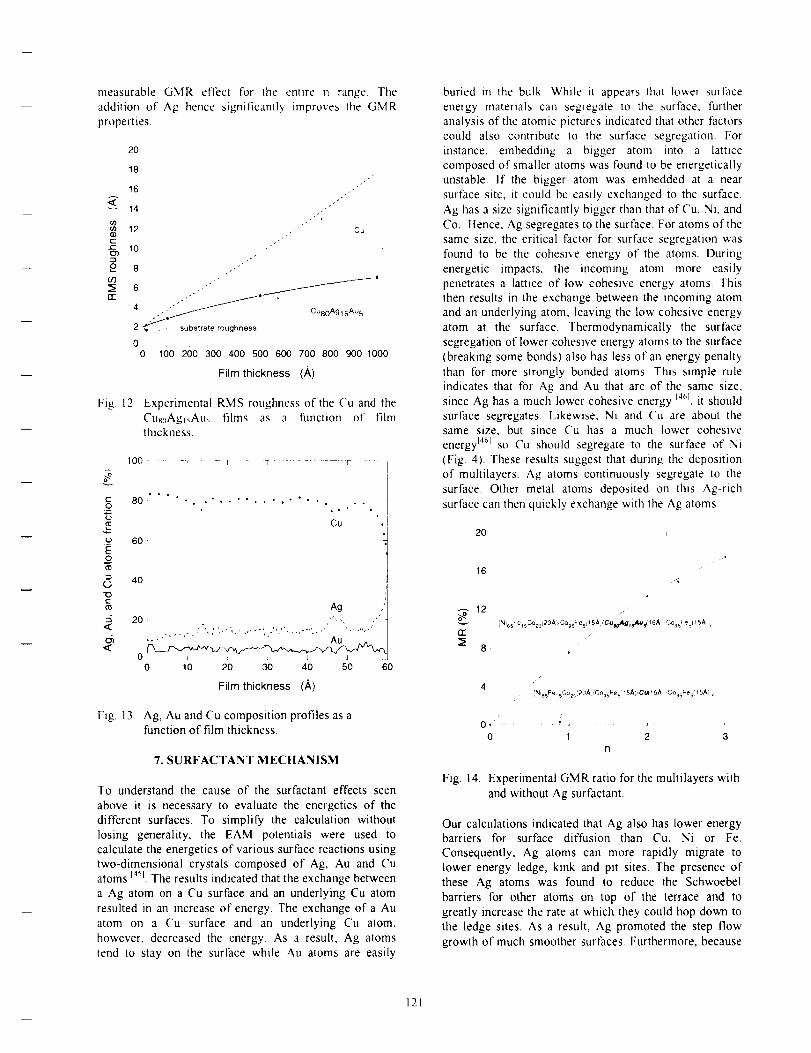
measurable GMR effect ['or the entire n range The
addition of" Ag hence significantly improves the GMR
properties.
cc-
O
n_
20
18
16
14
12
10 "/
8 .,'''"
6 "''''" m
2 _ substrate roughness
oo
Cu
Cu8oAg 15Au5
100 200 300 400 500 600 700 800 900 1000
Film thickness (A)
Fig 12 Experimental RMS roughness of the ('u and the
(-'u_Ag_Au_ films as a function of filmthickness.
o_
CO
-gO
(D
c
<6_
<
100 I
80"" "
6O
4O
2O
00
-_ - T T - T
° . " ° . ° ° ° , ° ° ° ° , • ° o .
Cu '. J
Ag ,"
10 20 30 40 50 60
Film thickness (A)
Fig. 13. Ag, Au and Cu composition profiles as a
function of film thickness.
7. SURFACTANT MECHANISM
To understand the cause of the surfactant effects seen
above it is necessary to evaluate the energetics of the
different surfaces. To simplify the calculation without
losing generality, the EAM potentials were used to
calculate the energetics of various surface reactions using
two-dimensional crystals composed of Ag, Au and Cu
atoms 14Sl The results indicated that the exchange between
a Ag atom on a Cu surface and an underlying Cu atom
resulted in an increase of energy. The exchange of a Au
atom on a Cu surface and an underlying Cu atom,
however, decreased the energy. As a result, Ag atoms
tend to stay on the surface while Au atoms are easily
buried in the bulk While it appears that lower surface
energy materials can segregate to the surface, [hrther
analysis of the atomic pictures indicated that other factors
could also contribute to the surface segregation. For
instance, embedding a bigger atom into a lattice
composed of smaller atoms was found to be energetically
unstable. If the bigger atom was embedded at a near
surface site, it could be easily exchanged to the surface.
Ag has a size significantly bigger than that of Cu, Ni, and
Co. Hence, Ag segregates to the surface. For atoms of the
same size, the critical factor for surface segregation was
found to be the cohesive energy of the atoms• During
energetic impacts, the incoming atom more easily
penetrates a lattice of low cohesive energy atoms• This
then results in the exchange between the incoming atom
and an underlying atom, leaving the low cohesive energy
atom at the surface• Thermodynamically the surface
segregation of lower cohesive energy atoms to the surface
(breaking some bonds) also has less of an energy penalty
than for more strongly bonded atoms. This simple rule
indicates that for Ag and Au that are of the same size,
since Ag has a much lower cohesive energy 1461 it should
surface segregates. Likewise, Ni and Cu are about the
same size, but since Cu has a much lower cohesive
energy 1461 so Cu should segregate to the surface of Ni
(Fig• 4). These results suggest that during the deposition
of multilayers. Ag atoms continuously segregate to the
surface• Other metal atoms deposited on this Ag-rich
surface can then quickly exchange with the Ag atoms
20
16
o_" 12 /•{N,6sFe1_Co2ci20ApOogs_esl_5Al_Cum_Igf_.4u#,16A C%5F esHSA)[ r
rr
8
{N esFet 5Co20{2 )AI,'Cn£sFesl ' 5A _CI._ '6A] CogsFe5fl 5A I_
0. i,0 1 2
Fig• 14. Experimental GMR ratio for the multilayers with
and without Ag surfactant.
Our calculations indicated that Ag also has lower energy
barriers for surface diffusion than Cu, Ni or Fe.
Consequently, Ag atoms can more rapidly migrate to
lower energy ledge, kink and pit sites. The presence of
these Ag atoms was found to reduce the Schwoebel
barriers for other atoms on top of the terrace and to
greatly increase the rate at which they could hop down to
the ledge sites. As a result, Ag promoted the step flow
growth of much smoother surfaces. Furthermore, because
121

energeticimpactreducedflatteningmoreeasilyoccursona surfacecomposedof mobileatoms,thehyperthermalprocessingconditionsthatcanleadtosmoothgrowtharereadilyaccessibleif aAg-richsurfaceis formedduringdeposition.Themechanismofrapidlysmoothingthelocalsurfaceasperitiesalsogreatlyreducestheprobabilityofcausingsurfaceshadowingduringobliquedeposition.Asaresuh,surfactantssuchasAgsignificantlyimprovethesmoothnessof the surfaceand the interfacesofmuhilayers
8. CONCIJUSIONS
The se0J-ch ota method f¢u the synthesis o! improved
quality GMR multilayers has been a prolonged process.
Atomistic simulation and accompanying experiments
have led to the discovery that control of adatom energy
and manipulation of surfactants can both significantly
improve GMR multilayer structure and transport
properties High adatom energy promotes surface
flattening due to enhanced surface reconstruction, but is
accompanied by interlayer mixing due to impact induced
atomic exchanges While a low combination of roughness
and mixing can be obtained at an intermediate adatom
energy, a modulated energy deposition scheme was found
to further reduce both the roughness and mixing. The
addition of surfactants such as Ag was found to lead to
significant flattening without intralayet energymodulation
9. ACKNOWLEDGMENTS
We are grateful to the Defense Advanced Research
Projects Agency (A. Tsao, D. Healy, and S. Wolf,
Program Managers) for their support of this work.
10. REFERENCES
M.N Baibich, J.M. Broto, A. Fert, F. Nguyen Van
Dau, F. Pel:off, P. Etienne, G. Creuzet, A. Friederich,
and J. Chazelas, Phys. Rev. Lett. 61, 2472(1988).
-_ S. Honda, S. Ohmoto, R. lmada, and M. Nawate, J.
Magn. Magn. Mater 126, 419(1993).
S.S.P. Parkin, Z.G. Li, and D.J. Smith, Appl. Phys.
Lett. 58, 2710( 1991 ).
J.C.S. Kools, J. Appl. Phys. 77, 2993119951.
K. Meguro. S. Hirano, M. Jimbo, S. Tsunashima, and
S. Uchiyama, J. Magn. Magn. Mater 140-144,
601(1995).
_' G.A. Prinz, Science 282, 1660(1998).
: S.SP. Parkin, R. Bhadra, and KP. Roche, Phys. Rev.
Lett. 66, 2152(1991).
s WH. Butler, X.G. Zhang, D.MC. Nicholson, and J.M.
Macl,aren, J. Magn Magn. Mater. 151. 354(1995).
_ P.M. Levy, Z Magn. Magn. Mater. 140-144,
485(1995)
" I).M.C. Nicholson. W.H. Butler. X.G Zhang. J M
Macl,aren, B.A. Gurney. and VS Speriosu. J Appl.
Phys. 76. 680511994).
_ J.P. Nozieres, V.S. Speriosu. B.A. Gurney. B. Dieny,
11. Lefakis, and T.C. Hnang, J. Magn. Magn. Mater
121,386(1993).
:-_ S. Schmensser. G Rupp. and A Hubert. J Magn
Magn. Mater. 166, 26711997).
_' XW. Zhou, and tlN.G. Wadley. m preparation
H T. Thomson, P.C. Riedi, and D Greig. Phv_ Rev
B50. 1031911994).
_ K.P. Wellock, BJ. Hickey. J. Xu, M.J. Walkel. and
N. Wiser. J. Magn. Magn. Mater. 140-144
58511995)
_ K.P. Wellock, B.J. Hickey, !) Greig. MJ Walker
and J. Xu, J. Appl. Phys. 75, 705511994)_7 D.H Mosca, F. Petroff, A [:ert, P.A Schroeder,
W.P. Pratt Jr., and R. Laloee. J. Magn. Magn. Mater.
94, LI11991).
_ JB. Youssef, K. Bouziane, O Koshkina. IlL (;all,
M.E Harfaoui, M.E. Yamani, J.M. l)esvignes, and A
Fert, J. Magn. Magn. Mater. 165. 28811997)
_'_ H. Zhang, R.W. Cochrane. Y Huai. M. Mao, X
Bian, and WB. Muir. J. Appl. Phys. 75, 6534119941
-_'_ Y. Saito, K. lnomata, and K Yusu, Phys. Rev B52,
6500(1995)
-'_ K. lnomata, Y. Saito, and S. Hashimoto, J Magn
Magn. Muter. 121,350(1993).
-'-_ K Kagawa, H. Kano, A. Okabe. A Suzuki. and K
Hayashi, J. Appl. Phys. 75. 6540(1994).
-" G. Rupp, and H.A M. van den Berg, IEEE Trans
Magn. 29, 3102( 1993 ).
_,4 HAM. van den Berg and G Rupp, IEEE Trans
Magn. 30, 809(1994).
-'_ G. Rupp, and K. Schuster, J. Magn. Magn. Mater.
121,416(1993).
__6 H. Ueda. O. Kitakami, Y. Shimada, Y. Goto, and M.
Yamamoto, Jpn. J. Appl. Phys. 33, 6173(1994).
27 R.J. Highmore, W.C. Shih, R.E. Somekh, and J.E
Evetts, J. Magn. Magn. Mater. 116, 249(1992).
-'s J.D. Kim, A.K. Petford-Long, JP. Jakubovics, J.E.
Evetts, and R. Somekh, J. Appl. Phys. 76,
6513(1994).
-_'_ H Kano, K. Kagawa, A. Suzuki, A. Okabe, K
Hayashi, and K. Aso, Appl. Phys. Lett. 63,
2839(1993).
_0 Y.G Yang, R.A. Johnson, and HN.G Wadley. Acta
Mater. 45, 1455(1997).
_: X.W. Zhou, and tI.N.G Wadley, Surf S_# 431,
42(1999).
_-" X.W. Zhou, and H.N.G. Wadley, Surf Sci. 431,
58(1999).
_3 X.W. Zhou, and H.N.G. Wadley, J. Appl Phys. 87,
8487(2000).
" X.W. Zhou, S. Subha, and H.N.G. Wadley, in
preparation.
_ H.N.G. Wadley, W. Zou. X.W. Zhou, J.F. Groves, S.
Desa, R. Kosut, E. Abrahamson, S. Ghosal, A. Kozak.
122

andI).X.Wang,Mat Re_ 5"o_. Svml_ Proc 538,
323_ 1999).
_s W. Zou, HN.G. Wadley, X.W. Zhou. D Brownell. S.
Ghosal. and R. Kosut. submitted to JVST.
_ M.S. Daw, and M.I. Baskes, Phv_. Rev. B29.
6443(1984).
_s R.A Johnson, Phvs Rev B39, 12554(1989)
_" II.N.G. Wadley, X.W Zhou, RA Johnson. and M
Neumck, Proj¢. Mater. S_i. 46. 329_ 2001).
_' X.V_ Zhou, I[.N.G. Wadley. R A Johnson, DJ
l,arson N Tabat, A Cerezo. A.K Petford-l,ong
G.D.W. Smith. PH Cliflon, R.I Martens. and'l.l
Kelly, submitted to Acta Mater
4_ X.W Zhou, and lING. Wadley ./ Al)pI. Phv._ 84
2301¢1998)
_" M. Parrinello, and A Rahman, J Appl. Phv._ 52.
7182(1981 ).
'_ X.W Zhou, and H.N.G Wadley. ,/ Appl Phys. 87.
553_2000)
4, T.L. Hylton, K.R. Coffey, M.A. Parker, and JK
Howard, J. Appl. Phys. 75, 7058(1994).
_" W Zou, H.N.G. Wadley, XW. Zhou, RA Johnson
D Brownell, submitted to Phys. Rev. B
" Metal Reference Book, 5th ed edited by Smith C. I
( Bt, tterworth, I.ondon. 1976)
123

t_
09"0iim
"609
0
0
c" .._C '--
-- t_
C
_'r"_a0
COt__
00
<
124
!
0
(I)
C)C
O9
c-Ot_(D¢/)
(1)Ii_6
S-Q..i..a¢0
_-o
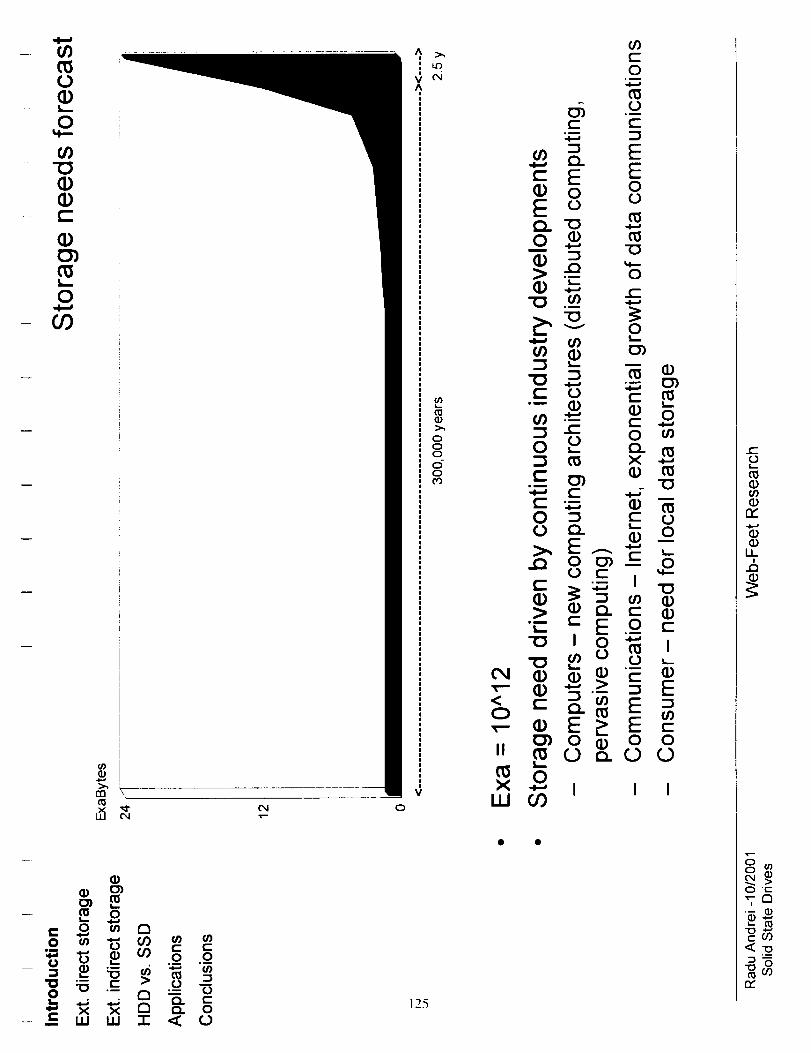
O
O
-OG)
C
G)
O
O9
A
^
OOO
oo¢O
M
G)
c-0
.o_
00E o oQ. "O ,_,o N _
8 _ E_
.= _-_-_o_
s_g_o_ 8oII _ O Q.
_5
>
08'§ _
n-

0
5,--
0
001,,,_
.m
"OI:::
.u
00
5_
: _e_./:-_I
0
00
• 0
t_00
t-O)
e- o -_"0
_. o L.)
0 0¢" X _
_ 0-_ 0 _
0
0
0 ._ 09
I
@ •
t-O
0_30
r_
00
LI_I
.Q
0 "C
"7,oo

E-__ ___ _'_ .___
__o .-izozz_:
_6
_)

_ C C
,_ ,¢,_n .o .o'6_ __-
_. 0 128- _ w 111 7- < o
, 0

¢-
E
EL't
nX
EL
F_ oX
×
×
uJX
.x2_ n.
S..
B __ __
E a ._
_: g_,, ,, ,, ,, ,,_ ,, ,,
0 _ _ I I I I I I I I
&
_ _'_" _+-- _ I.i.I -1- <_
ID
O"J.m
Ii
129
_6
>0 "t-
e_
'¢-o
0¢,0
r_

(/)C
_ •C_ \
0 0 0 0 0 C) 0 0 0 0 0(._ 0 (3*) O0 I'-- rid Lt) _ _ C',l ,r-
o _ _ _
-- _ W "I- _ 0
oo
Lt)000,1
00
00C_
cx,Ioo('Xl
aO9
oo(N
121121Z
130
E!,,,-
0
"0!,,,..
"0c
L,--
04.--
ES,--
0
• cCL •
o _-0 o-_ E"0 •• E0
._ ("
0 (_C)..
LL
"_ 0")
("" ._
• u)t_
-o • oCl _ o_Jc0 o_C _
' (II I ILl- 4--
t-O
0(/)0
n_
00
U-!
0 "r-
"7, O

c C
(D
_ _ ._o._o,_ _ _ _ -__.__ ._o . . a N _°_-_ X X _ O. 0
-- _ W W T _
131
II
[-.¢/J
•_ __
0 _ o o 0
¢-
c_
rY
ii
0 '_-
7-1D
0G)

CDE
t--
L_
- 0
I_ a
a
o_ o o
co co
o o o o o o
_F- _ o
_'_ _
o . m _ _°X X _ _'_ 0
_ c w w _ < o
ooc_
u_ooc'x#
O3"0
m
OO _ ¢"
o
_'- LL >00
_'__.- _.9 _
_ m
¢_ o 00 = ¢_ o.00 o..._ "0
•-_ _ 2_ .- ._ rr
m
o
c
+ooc_
87-
I
o
c
l--
tO
÷
132
r"o
o3
ur,¢'_
>
I

(/)o.rn
o o o o o ot.o o t.0 o t,o o0") 0") _ _ _ x-.-
(D
& &"
_, ,,,_ ,..,-
_ _ _ _ =_ __=o._R_
-- _ W W "r' ,_
oi.o
o
cOooc_l
i,oooc_
ooc',l
EimJ
(_m
m
I,,--
O.
"0(b(/)(II
.g "6 _
_> o_.-_
_._ (_ (n _.__- 0 h-T
0 rO _ <C (_
133
_6
I
e¢

- (I)
im
S,--
"0
LO
C_v
.m
c-O
.m
.m
CO0O_
0
0
n
f
O0 o
ol
s,..m
o fn
C0 _•_ _0in
"-_ 3 I
if)
_ _ "_ ,-.,-_ _ ,o .o
'_e,_ _ _ ___ ._o m _ =°"_" X X f'_ r_ 0
_ _c uJ uJ -I- <134
§

E
L..
O_
0C
E0
O_
0
#
/
O.
c_ o
0 _ 0 _ 0 t.e) 00") O_ _ T- T- 0 0
o o o 0 c_ o o
- ._ o
• _ .o .o
_ c w w -I- < o
00
E
o _CY
0C
0o _
ID
_m if)
+f'400
E--,1
00_ (2
C
o _g ®
8I
135
m
.0 Cmm m
•"_ 0
I,,....
> 0
"0 "0_D c
c
o • _
c o _z_A_ 0 •
_D_m 09 >n_ 00 o
AZ0
n_
(D
U_
_S
0 "_-
_cn
n_
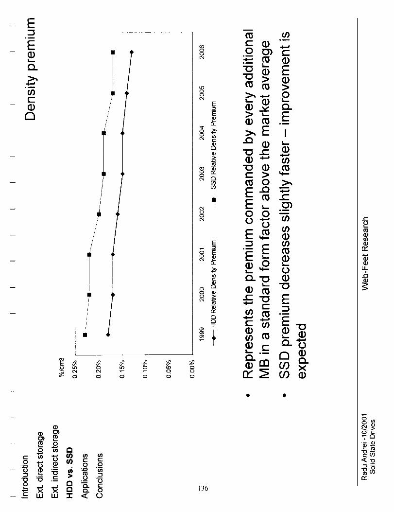
L_
Cl
>_
09c-(DD
!
m
I
/!
o_ o_ _ _ o_ o_
"" C_ CJ _'- T- 0 0o_ 0 0 0 0 0 O
(D
__ _ ,_ _ o o
____._ .__ -_O. 0
-- _ W W "I" _: 0
ooc_
oo
E
EID
c
.__
if)
OP4
E-1
c
o_o ID
_N
IDn-
O121n-
136
m
im
_ .__>.,E i
•_ _
_ .__
m_
f-O
11I
.Q
O "_
ne
(fJ00
._ _ .o .o
"_ Q. 0 137-- _ w w -1- < o
t-O
(Dt_
n,"
(D
1.1_!
>o
_m
r_

EE
c-(D
E
D a £3 £3a co a (D
I (D "i- CO
_Fo _
_ _ o.o-- iii "I" .Q_ S 138
g:
_5
>o 'r"
O0e==0
im
t_L==
im
C00
(==
(-=
Cim
0(==.(D_==
t_
(1)
oo
7-__ W
e-G
L.
b
b
_2
°,.._
b
r_°_
_2
139
©
0
°_
b
°_
b
r_
t'-t_
Ii!
>o .t-
ocO
c-O
mm
C
E
r_
r_© 0
:2
0
l-.9
"oo
_ 0
o (_ a,¢,,a
_ .__0
× × DLIJ U.I 7-
W
0 c._o
mu
c_. o 140
L,¢J
0
c-o
_J
(1)!.1_..&
_J0 "r-
_-o

c-O
,m
k...,
:3
t-O0
0
n,'
0..0
O)
•*-, 0 141_ c w w 7- ,_ o
0_0
t-O
_K
!
_0
>o _-

- O0im
c
m V
(/)
0(I,)
0
"0c-
E(I)"0m
- 0
I
CO
(/}
c
"occO
o"7 o0 o
0 0 0 0 00 0 0 0 00 0 0 0 0
CO000,I
o (_ t7
o.6 _ ._ *-• _ 0
::} .-- U
o "- 0 _. °• C:"-' X X (:::::) 0,. 0
_ c: uJ uJ 7- ,,,(
o
ooo,I
,_-ooo,I
eoooo,I
oTM
o
0
coeJ []
o oJo o
co00
o_
oi
OOO0
[]
142
00
i 0 _ _ 0
0I I I I
n."
<0
m
(_ e_l _--
I I I I
0
r_
0 '_--.
r_

...... !
v
!,.,.
0
C
E
m
0
- na
n
c-O._ 0 0 0 0 0 0
o o o o o oO O O O O
O
(OOO
tOOo CD
OOC_
U
o Oo
OC_
[KC.9o
o
O
°_ O_
o
I i ¢J
e5a
11)
o_

E3O9O9
0 C4- 0
X
z E
O"0n_
t-
dm
_ o g _-'_ • 0
"- "- _ _ ':o .o_•-- 0'),_o_Ol E _o
0 _..
o>0
:= E _ .EW o m oE "-'
t_mm
O 0 ct-- 0 ._ • t--
0 "_
:_ _- • 4-; _ .--
c t- 0 0 _ _w w < 0 r7 n" 0
0
_ " _ _ o
__'_- __ w uJ -1- < o
144
t-Of,--
0
0n-
o0
Ll_
_5
0 "r-

,m
8._70
Cv
0 _ --
_e
_g
0 1 I
g
8-- _ w w I145
I
8
,
QJ>
0 ,r-
O_
03<-o
n-

c-O
m
0C0
0
eo
o __ " _ _ _ o
_ o'6 ._ _
_ W W 7- ,_
c-
I=--
(-0")
_C
(P
Eim
1.0
0
c_
E "_
0 o _ o
'¢- O
o b "_ "" "-
09 1 I I09
146
00
>"r-
"Ta
c_
O9
_-o
_COe_

Non Volatile Memory Systems Design: Concept to
Reality and Trades along the Way
Author: Scott R. Anderson. Vice President SEAKR Engineering, Inc. 6221 S. Racine Circle, Centennial
co 8011 ], Scott_,seakr.com
Abstract--SEAKR Engineering is engaged in designing
and building memory systems using non-volatile memory
electronics. Primary targeted applications are highly
reliable spacecraft data recorders, aircraft reconnaissance
recorders, and board level products. This paper identifies
the steps that SEAKR takes in determining a preferred
system level solution and its implementation. Some key
obstacles encountered in past programs are identified
along with their solutions.
TABLE OF CONTENTS
1. 1NTRODU('TION
2. MISSION TRADE
3. MEMORY TECHNOLOGY SEI,ECTION
4. DEVICE QUAI,[FICATION
5. X2000 NVMS CASE EXAMPLE
6. ACKNOWI.EDGMENTS
1. INTRODUCTION
Due to their low cost per bit storage, mechanical based
data storage systems such as tape recorders and disk
drives have historically been the technology of choice for
remote data collection. Recent advancements in non-
volatile solid state memory technology have opened
opportunities for 100% solid state based solutions.
Nowhere is this more accepted than for applications
where maintenance is unavailable or mission failure is
quite costly. Key examples of such missions are
spacecraft and aircraft memory systems.
While solid state electronics are inherently more reliable
than mechanical based systems, a number of issues must
be addressed before usage of solid state can be assured.
One of the most critical items to address for spacecraft
applications are radiation effects and their impacts onnon-volatile solid state memories. JPI,'s X2000 is such a
program where non-volatile memory is to be used in a
Non Volatile Memory Slice (NVMS) under development
by SEAKR Engineering.
2. MISSION TRADES
Each application has its own unique mission critical
items. These critical items can be categorized as either
performance based or survival based. Performance based
mission critical specifications include items such as data
rate, data access time, operational scenario, operational
temperature range, power consumption, storage capacity,
size and mass. Survival specifications are primarily
environmental including radiation, shock, vibration,
temperature extremes, sah/fog, and dust. Most of these
critical mission items are extracted directly from
procurement documents, while some must be
experimentally derived.
Once mission critical issues are identified, a design team
commences a series of inter-related trades in an attempt to
achieve a paper concept that satisfies mission
performance and survival requirements at the lowest cost
& risk. At SEAKR, our preliminary 1fade teams are
composed of electrical design engineers, mechanical
design engineers, component engineers, and the technical
program manager.
Trades that are constantly performed for memory
technology are performance vs. cost vs. risk. For
instance, the newest memory technology consistently
provides higher performance over earlier generations.
However, it is rare that the newest state-of-the-art
memory technology does not need a costly qualification
effort. Furthermore, the immaturity of new technology
carries a risk that some unknown mechanism leads to
premature device failure in the intended environment. As
a rule of thumb, the latest state-of-the-art technology fairs
poorly in these trades unless performance cannot be
achieved with more mature technology.
On the other hand, if the intended product that the
memory technology is targeted for, has a long production
life, then the latest technology becomes preferred. This
reversal of trade results is primarily due to cost. For long
running production programs, obsolescence of mature
technology becomes assured demanding a qualification at
some point as newer technology is inserted.
147

3. MEMORY TECttNOLOGY SELECTION
Historically, non-volatile memory technology has been
more expensive, with lower performance, than volatile
memory technologies. These two critical facts have
limited technology trades such that non-volatile memo_
technology is only considered for those applications that
require data retention when powered down, or for
extremely large capacity systems that have very low
operational pov_'er consumption restrictions
Today some non-volatile memory technologies boast
single device capacities equal to volatile memory with
costs per bit comparable. Technology selection is now
made more on performance and intended application
rather than capacity and cost. In general, high data rate
systems with extensive read/write cycles are still best
satisfied with volatile memory technologies.
Once a memory technology has been identified, how the
device is to be packaged is addressed. Standard
commercial packaging is universally preferred if possible,
however, system mass limitations often dictate denser
solutions than standard packaging can achieve. In such
cases, stacked memory can be an attractive alternative.
SEAKR's preferred approach for stacked memory is to
procure stacked solutions from one of the many specialty
packaging houses, although in-house stacking is used
when extensive customer involvement is anticipated
specifications. More recently, automotive industry
standards have begun to be used to augment, and in some
cases replace historical approaches to device
qualification
Since most of SEAKR Engineering's applications are
high-rel, our device qualifications are more extreme than
desk top or benign applications require. A typical device
qualification program includes 1000 hours of elevated
temperature life testing, 100 temp cycles from 55 ° C to
+150 ° C, solderability, salt spray, shock, outgassing, and
resistance to solvents.
In addition to the above qualifications tests for all high ret
applications, for spacecraft applications, the most
interesting survival requirements arise due to the radiation
environment and long mission life.
5. X2000 NON-VOLATILE MEMORY SLICE
CASE EXAMPLE
In the spring of 1999, SEAKR Engineering was selected
to develop and manufacture a number of 256 Mbyte non-
volatile memory boards compliant to the Compact PCI
bus protocol. Missions targeted by JPL for use of the
X2000 NVMS include a science collecting experiment
around Jupiter's moon Europa. The radiation environment
at Europa is extreme with ionizing radiation exposure for
the mission exceeding hundreds of thousands of rads St.
In addition, high energy, heavy ion particle bombardment
is also present. Our task was to identify a solution and
qualify a non-volatile memory technology that willsurvive this extreme environment
4. DEVICE QUALIFICATION
If not previously qualified, once a preferred memory
technology and packaging approach has been identified, a
qualification program is initiated. Device qualification is
primarily focused on demonstrating robustness and ability
to satisfy survival requirements. In general, a
qualification program follows established military
Initial technology evaluation efforts targeted technologies
with inherent immunity to radiation effects. These
technologies included GMRAM, specifically radiation
hardened EEPROM, and FRAM. Unfortunately, these
technologies were low in density, extremely expensive, or
carried a high risk factor due to immaturity. Our
technology trade then shifted to more commercial
148

technologieswithFlashEPROMemergingasa likelycandidate.WeselectedseveraldifferentFlashEPROMdevicesfromseveraldifferentmanufacturersandwithassistancefromJPLperformedradiationtesting.ThesetestingsincludedexposingdevicestoTotalIonizingDose(TID)radiationandheavyions. Resultswerenotencouragingas FlashEPROMdevicesshowedTIDradiationfailuresoccurringatlevelswhichwereorders-of-magnitudesless than the expectedenvironment.Furthermore,someof the [:lashdevicesrevealedsensitivitytodestructivelatchupinducedbyhigh-energyparticles.
Undernormalcircumstances,thesensitivityoftheFlashdevicewouldhavedisqualifiedthemfrom furtherconsideration,however,theperformanceandcostimpactsof usingotherapproachesencouragedustocontinueourevaluation."I'hree strategies were undertaken in an
attempt to qualify the flash device for X2000:
1) Closer examination of the true enviromnent that the
devices would be in.
2) Further testing to determine if any operational
constraint or system design approach might improvetolerance.
_,) Modification of the environment through the addition
of shielding material in an attempt to lessen ionizing
radiation exposure
Once it was determined that the Flash devices could not
achieve mission TID requirements, our customer, JPI.,
performed detailed sector and shadowing analyses on the
spacecraft and X2000 processor that our NVMS would be
inserted into, and determined a lower TID exposure level
than originally expected In conjunction with this effort,
we resumed radiation testing while modifying the
operational mode of the devices. We determined that by
power cycling the devices, rather than maintaining them
at 100% duty cycle, their tolerance to TID could be
dramatically improved. Furthermore, we determined that
by inserting current limiting resistors, destructive latchup
could be prevented on some manufacturer's devices
With this improved information, we were able to identify
that by adding additional spot shielding at the Flash
device, we could achieve mission survivability.
In addition to radiation induced device failures, the Flash
devices have a wear-out mechanism that limits life and
they have demonstrated random loss of data known aserratic bit errors. For a mission critical function such as
our NVMS, such loss of data is unacceptable. Our
solution was to develop a novel error detection and
correction (EDAC) circuit design which fully corrected
large block failures as well as the erratic bit errors and
soft single event upsets. Diagnostic routines can be
implemented by the user to determine if the erroneous
data is due to a hard permanent device failure or just a
random single event effect. For soft single event effects,
the data can be corrected and rewritten effectively
removing the error. For hard failures, the corrected data
can be v_ritten into unused nev, memory locations and the
old failed memory "'mapped" out of usable address space
6. A('KNOWLEDGMENI'S
SEAKR Engineering would like to express our
appreciation to Valerie Thomas, Karl Strauss, Audrey
Doran, Gary Swift and the rest of the JPL X2000 NVMS
team for their assistance and teamwork in successfully
developing the X2000 NVMS.
149

SESSION #4: ApplicationsThursday, November 8, 2001
10:50 AM - 12:00 Noon
Chair: S. Anderson, SEAKR Engineering
10:50 AM
ll:10AM
11:30 AM
Experiences in Qualifying a Commercial MNOS EEPROM for Space;
E. King, R. Lacoe, G. Eng, and M. Leung, The Aerospace Corporation
Neo-Stacking of Packaged Flash Memory; K. Gann, Irvine Sensors
Corporation
High Speed MRAM Buffer for High Capacity Non-Volatile Shock
Recorders," R. Sinclair and R. Beech, NVE Corporation
150

< ,"---J/' _ //
<'-', 0 .... :. /
i
Experiences in Qualifying a Commercial MNOS
EEPROM for Space
E E King, R C Lacoe, G Eng, and M S Leung
The Aerospace Corporation
2350 E El Segundo Blvd
(310) 336-7898, everett e king@aero org
AbstractfifiQuahfying a commermal Non-Volatile
Memory. (NVM) component for space poses several
challenges detailed reformation about the process and
design is not hkely to be available, long-term reliability
data are uncertain or insufficient, httle, if any, radiation
data exist; and the data retention reqmrement for a space
applicauon generally exceeds ten years In this paper, we
describe our experiences m qualifying a commercial l-
Mb]t EEPROM (the ltitachi IIN58CIO01) for space
Since the umque attribute of a NVM is its ability to retain
stored data over long periods of time with no power
applied to the component, our work focused on
determining the data retentmn lifeUmc and developing a
procedure to screen potential earl), failures from the part
popular]on
The MNOS trans]stor Ls programmed to a el i by applying
15 V across the gate insulator 5 V to the gate, and about
ill0 V to the body (well) Under this bias condmon,
electrons are injected into the gate insulator from the
channel, where some of them are trapped (stored) in the
electron traps that are inherently found m sihcon nitride
To erase this eli (program a e0i), the fil 0 V bias is applied
to the gate and 5 V is applied to the well Under this bias
condition, holes are rejected into the gate insulator from
the silicon substrate where they neutralize the trapped
electrons The ill0 V bias is generated by an on-chip
negative high-voltage generator c_rcu]t The erase/wr_te
nine is about 10 ms, and is controlled by an on-chip rimer
A sense amphfier discriminates between the written and
erased (el i and e0i states, respectively) states
TABI.E OF CONTENTS
1 INTRODUCTION
2 EXPERIMENT
3 SCREEN DEVELOPMENI
4 CONCIJ_JSIONS
5 REFERENCES
6 ACKNOVv'I.EDGMENTS
I INTRODUCTION
The tIN58ClO01 _s a 128k by 8 bit electrically erasable
and programmable read-only memo_ The part ]s
fabricated usmg a CMOS process with the addmon of a
Metal-NitrMe-Oxlde-Sihcon (MNOS) transistor that ]s
used as the data storage element [1] The MNOS
trans]sto) is schemat]cally illustrated m Figure 1 A data
bit Is stored m the MNOS transistor m the form of charge
that Is trapped m the silicon mtride film that is formed
above the channel The presence or absence of charge
results in a change m threshold voltage between two
states that are defined as a eli and e0i The transistor _s
interrogated by detecting the channel current that flows
when the gate voltage ]s set at 0 V
.Memory gale
." _; ' ...
P-wel| Si02 : 1.6 nm
N - substrate
Figure 1 Schematic ]llustratmn of the type of MNOS
memory transistor used for the HN58C l O01
The memo_' exhlb,ts a high degree of non-volauhW due
to the retentmn of the trapped charge m the gate insulator
even when the power to the device is turned off The
memory_ transistor is not totally nonvolanle, however.
because the trapped charge (whether holes or electrons)
leaks out of the mmde over time, resulting in the decay of
fl_e programmed threshold vohage The dominant charge
decay mechanism for the MNOS transistor has been
151

foundto bethermalemissionof thechargeoutof thetraps[2] Theretentionofthenettrappedchargecanalsobeimpactedbyanexposuretoionizingradiation,becausetheelectron-holepairswhicharecreatedbytheradiationcanalsobecometrapped,therebychangingthethresholdvoltage
2. EXPERIMENT
There are three unique characteristics of an MNOS
memory device programming speed, data retention, and
endurance In the primary application under consideration
here, data retentmn was the key characteristic of interest,
since the memoLy was to be written at the beginning of
the mission (before any aging or radiation-induced
degradation of the part had occurred) and no rewriting of
the memory was planned during the mission The purpose
of our experiments was to verify that these memory
components were capable of retaining data throughout the
mission and to develop a test that could be used to
eliminate parts from the part population that were prone
to early failure As a result, we conducted aging tests,
total lomzing dose radiation tests, and a variety of
electrical tests on the parts
Accelerated,4gmg 7_,sts The usual method to determine a
dewcc-agmg characteristic of a component is to attempt
to accelerate the failure mechanism by thermally stressing
the part in an oven Temperature accelerated aging
assumes that the intrinsic device life is limited by a
thermally accelerated process that can be characterized by
an acUvatmn energy, and that no intervening processes
occur between the accelerated aging temperatures and the
lower device use temperatures that would cause the
extrapolation of the high temperature data to the low
operating temperatures to be incorrect Based on both the
intended application and the obJective of isolating the data
retennon hfeume of the MNOS transistor from any aging
of the peripheral circuitry, our aging tests were conducted
without power being apphed to the part
the manufacturer claimed that this MNOS memory was
capable of retaining data for 20 years There were two
issues with accepting this lifetime value First, it is based
on an activation energy of 1 1 eV for charge leakage from
the storage transistor; whereas, _t _s generally
acknowledged that charge leakage is characterJzed by a
range of acmatlma energies rather than a single value [2]
In fins case. it _s m_portant to know the minimum
act> auon energy to be able to predict that the parts will
meet the data retennon mission requirement with high
confidence Second, the manufacturer did not disclose the
failure criteria that had been used to determine his
actxvauon energy Because of the exponenual relationship
between activation energy and lifetime, even a small
change m the choice of activation energy can result m a
change m hfctlme prediction of an order of magnitude, ormore In this work, therefore, we conducted thermally
accelerated aging tests both to determine a worst-case
actlvatmn energy, and to collect degradation data that
could be used to predict the data retention lifetime in the
application
Our part population consisted of 21 commercial parts in
plastic (epoxy) 32-pin dual ln-hne packages The parts all
had the same date code We wanted to expose the parts to
a relatively high temperature to accelerate the time-to-
failure and shorten the test time, however, there was a
concern that the parts would fail because of the plastic
package if the oven temperature was set much higher than
the spemfied maximum storage temperature, which was
only 125 C However, tests on the plasUc packaging
material showed that it could withstand exposure to
temperatures up to 275 C before decomposing As a
result, we felt comfortable with using a maximum
temperature of 200 C in our accelerated aging tests
Therefore, since data at two temperatures are necessary to
determine an activation energy, accelerating temperatures
of 175 and 200 C were chosen for these aging tests Of
the 21 parts in our population, 10 were aged at each
temperature and one was used as a control
The parts were preconditioned by writing them with an
alternating set of checkerboard (CKBD) and reverse
checkerboard (NCKBD) patterns a total of 220 times,
checking them for any failures after each write ttalf were
begun with a CKBD and the other half with an NCKBD
The parts were then soaked m a 150 C oven for 48 hours.
and re-tested The final pattern written into a part prior to
the aging test was the reverse of the last written pattern so
that there would never be more charge stored on a
memory transistor in the part than that assocmted w_th a
single write
The parts that were aged at 200 C were pulled out of the
oven and tested after every four hours, while the parts
aged at 175 C were tested at 22 hour intervals l'oward the
end of the aging tests these times were extended since no
failures had been observed and it was very much desired
to determine a tlme-to-fadure from these experiments
before the end of the project
During these tests, however, no spec_ficatlon failures
were observed for final aging times of 755 and 1305
hours at 200 and 175 C. respectwely While finding no
errors was posmve in some respects, these results did not
provide an,,' failure data from which to determine the
achvahon energy or predict the lifetune at normal
operating temperatures On the other hand, we did collect
parametric electrical charactenzatmn data on the parts
during aging from which we could draw conclusions In
particular, the readout access hme (time fiom chip enable
assertion to valid data out) turns oul to be sensmve to the
charge flow through the memm5 _ transistor when _t _s lead
out This allowed us to use measurements of the number
of errors versus the chip enable access time to estimate a
tlme-to-thflure at each of our accelerated aging
temperatures Examples of this errol dlsmbutlon dam (t"ol
152

one quarter of the partis addresses) for two parts, one
exposed to 200 (7 and the other to 175 (2, are shown m
Figures 2 and 3, respecnvely
The push out of the access time with thermal exposure
can be clearly seen in these figures; although, there is still
considerable margin at the times measured to when the
access time would have failed the manufactureris
specificaUon llmm which is at 150 ns I1 is not obvious
how to use these push out data to calculate the data
retention lifetime, due to the pronounced ledges that
develop over the course of aging in the error distributions
These ledges appear to be primarily due to varianons inthe stretch-out associated with individual Data 1/O hnes
For example, Figure 4 shows the error distribution for the200 C error distribunon curve measured at 533 hours that
IS shown in Figure 3 broken into the error distributions for
each of the eight Data 1/O lines We conclude that the
large ledge that occurs at 8000 errors m Figure 4 is
primarily due to the behavior of the Data 1/O3 line m this
part Furthermore, this ledge, in combination with one or
more of the even numbered Data I/O lines (which will add
to the number of failures observed for DIO3 because an
even number output will tend to fail on an address for
which DIO3 passes) also produces a ledge at 16,000errors Other variations m the access rime failures
between these ledges are probably due to slight
differences m the propaganon delays to the various
memory_ transistors These variations will stretch out the
portions of the curves that lie between these ledges
35000
30000
25000
0
20000W
150006
z 10000
5000
0 -
70 80
-__--" -- Control-Q2
'_, ' 553 hours
951 hours
1036 hours
t 1305 hours
",, Rewritten
tl t /I_1
90 100 110
CE Access Time (ns)
Figure 2 Number of errors m the second quarter of the
memor?_' address space for an example part versus the chip
enable access time. w=th aging time at 200 C as a
parameter
It is a good assumption that a large percentage of this
observed access trine stretch out is caused by charge
leakage off of the MNOS lnemo_' transistors
Unfortunately. other factors are also likely to be revolved
m the stretch out, not the least of whch might be
153
variations in the sense amps, whose characteristics
determine how long it takes for them to determine
whether the current out of the MNOS transistor Is a eli or
a eO i In general, then, the stretch out m access time will
be some combination of how much charge was initially
stored in the memory transistor, how much charge has
leaked off the memory transistor during aging, the
characteristics of the sense amp associated with that
memory transistor_ and, probably to a lesser extent.
variations in propagation delay related to the decoder
circuitry and output amphfiers
To determine an acnvation energy for the charge leakage
mechanism, data should be used for which the
degradation is due solely to charge leakage Arguably, the
best we can do with the number of errors versus access
time data we have is to estimate the number of hours it
takes at the two test temperatures to produce the same
push out of the access time, and to then use these two
temperatures and times to calculate an acnvatlon energy
For example, we see in Figures 2 and 3 that the error
distribution at 226 hours at 200 C is similar to the error
distribution at 1305 hours at 175 C An analysis of our
data using this approach establishes a time-temperature
eqmvalence that results in an activanon energy of about
12 eV for charge loss/data retention This value is
consistent with, but _s a bit higher than the manufactureris
value of I 1 eV
35000
30000
25000
9 20000
w
• 15000oz
10000
500O
70 80 110
-- Control-Q2
162 hours
[ -- 226 hours
-2.Z':,,,.
g0 100
CE Access Time (n$)
Figure 3 Example of data similar to that shown in l:lgure
2 except that the aging temperature was 175 C
We can now predict the data retention lifetime at 70 C
based on the worst-case data push out rate measured at the
two aging temperatures using this 12 eV activation
energy The estimated rime-to-failure (where fadure is
defined as the point at which the access time reaches 150
ns) is found to be a few hundred years using this
approach, which is well beyond the mission reqmrement

Tolendcredibihtytotheassumptionthattheaccesstimepushoutwasdueonlytochargeleakageoffthememorytransistorandwasnotcausedbycircuitdegradation,thepartswererewrittenandtestedaftertheseagingtestsAllpartscontinuedtomeetspecificationandallaccesstimesreturnedtotheirinitialvaluestowithin1ns
18000
16000
14000
12000
o
10000w
80006Z 6000
4000
2000
--DIO7
DIO6
DIO5
DIO4
DIO3
DIO2 , \
\DIO1
-- moo
70 80 90
CE Access Time (ns)
\
100
Figure 4 Example of the number of address errors versus
the chip enable access time for each Data I/O line Data
correspond to an aging time of 533 hours at 200 C, which
is shown in Figure 2 for the combined Data 1/O lines
]'he acUvauon energy for de-trapping charge m silicon
nltride given m the literature is 0 35 eV [3] Even when
we use this worst-case activaUon energy to describe the
charge loss m the memory transistor, the predicted time-to
failure at 70 C based on extrapolating our access time
push out data to failure ( 150 ns) is 52 years
Even though we did not find any failures in our small part
population during these aging tests, a review of other data
in the community suggested that there was a finite
probability of having, perhaps, 1 part in 30 faihng earlier
than those in the normal population The one intermittent
failure we saw in our aging tests, which is described
below, also raises a concern of an early failure issue
Obviously such an early failure would pose a great risk
for a space application Therefore, a considerable effort
was invested in developing a stringent test to screen parts
subject to such early failure out of the production part
population
Iota/lontzmg l)ose Tests
Since power was only rarely to be applied to these
memory parts during the mission under consideration, the
parts were irradiated unbiased (all leads shorted together)
The same parts used in the accelerated aging tests were
rewrmen with a complementary checkerboard pattern and
lrradmted in a Co-60 source at a dose rate of 3
krad(Sl)<mmute to 78 krad(Sl) in 26 krad(Si) increments
No significant degradation was observed after 78
krad(Si)
154
Parts were then divided into two groups and a second
aging experiment was begun using temperatures of 175
and 200 C Although these aging tests were not carried
out as long as the original aging tests, the push out of the
read out access times for the times we measured were
essentially the same For example, the average change in
access time during the post-irradiation aging stress at 157
hours at 200 C was 102 ns This value compares
favorably to the average change in access time of 10 0 ns,
which was found after 162 hours m the 200 C tests that
had been conducted prior to the irradiation
A word of caution based on experience with other part
types, the on-chip bias generator is likely to fall at
relatively low total dose levels when the part is irradmted
trader normal operating voltage conditions Such bias
generator circuits are known to fail at levels in the range
of 10 to 20 krad(Si)
]ntermtttent Errors
Some anecdotal data about this part type raised a concern
that it was prone to an intermittent failure problem
During our aging test, we saw two instances of an
intermittent error problem w_th one part that may have
been the same problem that had been reported by others
In the first instance of this part falling specification, the
failure was repeatable over a period of a few hours, but
the part passed with no problem the following day In the
second instance the part continued to fail over a two day
period, glwng us a chance to characterize the failure
behav]or It was discovered that the failure was sens]tlve
to power supply voltage, passing at 5 25 V. being
marginal at 500 V, and consistently failing at less than
5 O0 V Scope traces of the data signals from Data I/O1
and Data I/O2 for normal (passing) operation are shown
in Figure 5 At this voltage, the data are correct (Data
!/O1 is a e0i during the first clock cycle and a eli during
the next, while Data 1/O2 is the inverse of Data !/O 1) The
Data I/Ol and 2 signals are shown in Figure 6 for a power
supply voltage of 4 65 V, for two addresses where a
failure is observed In this case, Data 1/O 1 should be a el i
followed by a eO,i whereas Data 1/O2 should be the
reverse of Data I/O1 The problem is a failure of either of
these Data l/O signals to go to a e0i state at these two
addresses Note that m the first pattern shown in Figure 6
the Data I,/O2 signal does go to a e0,i but only after a tune
has elapsed that ]s well beyond the specified access t]meof 150 ns Th]s failure behavior was not observed on the
following (third) day
There are several features of this intermittent failure
behavmr that seem tmportant F_rst. this behavior was
only seen with aged parts, which implies that _t is the
result of charge leakage off of the memory transistor
Second. the failure is always due to a Data I/O line not
making 11 to a eOi level. _mplymg that the problem _s
related to the electrons, rather than the holes, leaking oul

of thetranststorisgateinsulator Third. only a small
number of addresses fall, implying that the problem is
dominated by a few memory cells, rather than to a sense
amplifier, or some other pan of the circuitry, such as an
output buffer Fourth. the oscillations suggest that there
may be an occasional combination of degraded memory
transistor and sense amplifier that produces an instability
of the overall data readout behavior On the other hand, it
is not at all clear what would cause this failttre behavaor to
disappear after a few hours if it is due only to charge
leakage from the memory transistor, since no known
mechanism is known that could replace this charge in the
gate insulator short ofreprogrammmg
reK Stolz Sir_gl_ Seq 50OMS/S
' +_ _ . 7 --
,__ .,, i .........{r,_ 2 O0 V C_4 2 O0 v
"1 56g#s
14 Mar 2000
1208 42
Figure 5 Scope trace of the part experiencing the
intermittent failure The power supply voltage is set at
5 25 V. where the data outputs are stable and correct The
scope traces from top-to-bottom are Output Enable, Data
I/O1. Data [/02, and Chtp Enable
' _tO[, _rl_te SeQ I OOCS,%
•t i i',4....: " i , i 1
1 i;ilt'_r " ; '',iii,_i, i ,}
f _ [,11_1: ; ! r !'-_"-t
Figure 6 Scope trace showing the intermittent failure In
this case the power supply voltage is set at 4 65 V The
oscillations that occur on both Data I/O1 and 2 can be
seen. as well as the delay' m Data 1/O2 transmomng to the
e0i state
155
It should be pointed out that there was a concern that this
intermittent failure might not be due to the chip inside the
package, but to a corroded package pin, or to some other
test fixture-related problem However, neither cleaning
the pros, repositionmg the part in the socket, nor adjusting
the fixture solved this problem The facts that no other
part in our test population exhibited this behavior and that
only a very few of the addresses on the part that exhibited
the intermittent behavior failed, further support the
conclusion that this was not a pin or fixture problem, but a
chip related problem
3_ SCREEN DEVELOPMENT
A major program objective was to develop a test that
could identify parts that were either weak m terms of their
data retention capability, or were prone to the intermittent
failure behavior described above The approach taken was
to make sure that this test included all of the worst case
operating conditions we could identify The operating
conditions we identified as being most important were the
test pattern, the power supply voltage, and the
temperature
Power Supply [bltage and Temperature
Parts were routinely tested at 4 5. 5 0, and 5 5 V
Although parts did not generally fail specification, onecould see from the error distribution versus readout access
time data that the push out was worse at 5 5 V than _t was
at 4 5 V This is counterlntmt:ve, since CMOS circuits
generally operate faster as the power supply is increased
In this part, however, it ts suspected that the threshold
level of the sense amplifier _s higher at the higher power
supply voltage, increasing the nine 11 takes to integrate
charge from the memory transistor and determine _ts data
state
On the other hand. we found in tests conducted after those
described above that one additionally aged part exhibited
a few hundred access time failures when tested at room
temperate and with a power supply voltage of 5 5 V In
this case, the part did not exhibit errors at 4 5 or 5 0 V In
addmon, the errors decreased m number as the
temperature was increased, completely disappearing at a
temperature of about 38 C This behavior was
reproducible over a several week period
Test Pattern
A test pattern sensitivity was also found in later tests of
our aged parts An analysis showed that an error was
strongly correlated to the data that had been previously
readout In particular, reading out a data byte having a
high number of ells was found to significantly increase
the probability that a e0i bit m the next bytc would be
readout incorrectly For example, the probability of
reading out an error m a data byte was found to increase
by' over 70% if the data m the prior byte was the worst-

casepattern,el111I I 1I i Thesepatternsensitivityerrorsarenotsolelydueto chargeleakageoff therelatedmemorytransistors,however,becausethe dataaregenerallyreadoutcorrectlywhenthepatternis runbackward
Basedonananalysisofthispatternsensmvlty,aspecialtestpatternwasdevisedthatwasintendedtoimprovethediscriminationofweakpartsinthepopulationoverthatofacheckerboard,orothersimplepatternFirst,wewantedtoheavilypopulatethepatternwithe0is,sinceit isabout26,000timesmorelikelythatae0ibitwill fallthanaelibit Ontheotherhand,wewantedto inserta shortsequenceof patternsperiodicallyin thememorythatincludeddatabyteswithseveralelis toallelissothatwewouldincreasethelikelihoodof detectingthepatternsensitivefailuresthatwedescribedaboveFinallyweincludedauniquecodewordlocatedateachAddressbitsothatthepartcouldnotpassthefunctionaltestunlessevenaddressbittoggledIt wasestimatedthatthisnewpatternwassome300t_mesmorelikelytodetectanerrorthanthecheckerboardpatternthathadbeenusedinitially
4 CONCLUSIONS
Tests were conducted to verify that the Hitachi l-Mblt
(128k x 8) MNOS memory component, the HN58CIO01,
was able to retain stored data for periods as long as the 20
years specified for this part and after exposure to a
specified total ionizing radiation dose In addition, a test
was developed to screen parts out of the population that
were subject to either premature or intermittent failure
,_.ccelerated aging tests showed that the activation energy
for charge leakage from the memory transistor was about
I 2 eV This result combined with push out of the read out
access time at 175 and 200 C suggested that the nominal
data retentmn time for this part is well over the 20 years
specified, as long as the temperature remams below 70 C
Total ionizing dose irradiation tests showed that the part
was msensmvc to a dose of 78 krad(Si) (unbiased
irradiation) Subsequent aging tests on the _rradiated parts
showed that the radmtion had little, if any influence on
data retention
A test was developed to screen parts that might be prone
to early or intermittent failure out of the population A
high percentage of the memory was written w_th ef)is,
since a el i rarely', if ever fails A sub-pattern was written
periodically throughout the memow address space to
detect a pattern sensmvlty that was found in which
failures were observed m a word having a high number of
iOis being readout after a word having a high number of
el is To increase the likelihood of finding a readout
failure, this functional test should be performed wqth
power supply voltages of both 4 5 and 5 5 V and at room
temperature (or lower), rather than at an elevaled
temperature Even though we feel that this test will
increase the probability of findmg parts prone to early'
failure, there is no guarantee that the screen wdl be
successful, since the physical mechanisms responsible for
early failures are unknown and we were not able to
demonstrate the proposed test on a significantly large part
population
5. REFERENCES
Kamigaki, Yoshiaki, et al, i Yield and Rehability of
MNOS EEPROM Products,i IEEE,]. ofSol.-State
Cwcults, Vol 24, No 6. December 1989, p 1714
McWhorter, P J, S L Miller, and T A Delhn,
i Modehng the memory, retention characteristics of
silicon-nitnde-oxide-sihcon nonvolatile transistors in
a varying thermal environment,i ,L4P. 68 (4), 15
August 1990, p 1902
Wu, Ken, et al. iA Model for EPROM Intrinsic
Charge Loss through Oxide-Nltride-Oxide (ONO)
lnterpoly Dlelectric.i IEEE Proc. _?/the IRPS. 1990.
p 145
6 ACKNOWLEDGEMENTS
We wish to acknowledge the support of the Aerospace
IR&D program, as well as insightful conversations wqth
Craig Sather and Tom Tsubota
156

--'2 7/ / '/
,//J
Neo-Stacking of Packaged Flash Memory
Keith D. Gann
Director. High Density ElectronicsIR VINE SENSOR,{; CORPORA TIOX
Tel.: {714} 444-8765 3001 Redhill Ave., Bldg. 4t:ax: (714) 444-8865 Costa Mesa, CA 92626-4532
kgann%irvine-sensors.com www.irvine-sensors.com
Abstract--A variation on lrvine Sensors' Neo-Stackingprocess allows extremely dense packaging of Flash orother memory while sidestepping the problems associated
with obtaining Known Good Die (KGD). Memory isoften difficult or impossible to obtain in die or waferform, and comprehensive testing and burn-in isprohibitively expensive for many applications. Readilyavailable plastic encapsulated packaged memory chips arepre-tested and can easily be further tested and screened,speed sorted, tested over a different temperature range,etc. tlowever, they cannot be packaged densely enoughto meet the requirements for many applications. Thispaper describes a method for reprocessing and stackingstandard packaged memory, along with support circuitry,into a chip-scale footprint with a very low profile.
TABI,E OF CONTENTS
1 INTRODUCTION2. NEO-STACKING3. STACKABI,E LAYERS FROM TSOPS4 COMBINING TECHNOLOGIES
5 SUMMARY
1. INTRODUCTION
Often, flash memory is most readily available in a plasticencapsulated thin small outline package (TSOP).Processes for stacking TSOPs are available from severalsources, Irvine Sensors Corporation among them. Theprocess is economical and allows two to eight chips to use
the board space of only one. However, the overallvolume is not reduced since the stacked TSOPs, plus
interposers, form a relatively tall subassembly. For manyapplications, stacking TSOPs provides the needed density,although for extreme miniaturization, stacking baresilicon chips is required,
lrvine Sensors Corporation has established processes forbare die stacking that require that the chips be available ineither die or wafer form. Obtaining chips in either form issometimes difficult or impossible. When bare die are
available, an important design issue to be addressed is thatof Known Good Die {KGD). Generally, KGD solutionsare rather costly. The problems of bare die availability
and KGD testing can be addressed simultaneously.
TSOPs are the most readily available part type, and theyare already fully tested in that packaged format. Theprocess being developed further processes the TSOPs intosmaller, very thin, stackable layers.
2. NEO-STACKING
Irvine Sensors' Neo-Stack TM process starts with a bumpedKGD that is encapsulated in a potting compound. Thinfilm metal traces contact the 1/O bumps and route the
signals to the edges of the potting material. The layer isground from the backside resulting in a thin (.25 mm to.10 ram) complete layer, as shown in Figure 1,
Figure 1: Neo-Layer
,/" Trace
: /
/°o
//
°/°°
\•,, ,Flash Memory / Compound
• .°
"',... Chip (thinned).,..-/
A Neo-Stack is created by laminating Neo-Layers with a
cap substrate, which uses through-holes to provide I/Opaths. Bus metalization is applied on one or more sides tointerconnect layers and the cap substrate. Theintersection of the layer traces and the bus traces form the"T-Connects", which are key to high reliability. Unlikewrap-around or "'L-Connect" approaches where stepcoverage problems can result in a reduced metal crosssection, the trace thickness of T-Connects remain the full
thickness as deposited. A complete Neo-Stack is shown
in Figure 2.
157
Figure 2: Neo-Stack
I
I
Substrate I
i"'\ i
\ i"\ I
\i
i
\
)
"T-C_nnect"
/"/
4. C()MBINING TECHNOL()GIES
The material compatibility allows layers made lTomTSOPs to be stacked along with standard Neo-kayers,which can contain different die types. The only constraintis that the die types in the Neo-l.ayers must not be so
large that the Neo-Layer becomes larger than the memorylayers. This is normally not a problem because memorydie sizes are usually quite large as compared to other chiptypes in a typical subsystem.
Irvine Sensors is currently developing two products usingmodified TSOPs combined with standard Neo-l.ayers.
The first is a stack for the mass memory storage portionof a miniature stacked computer. A single Neo-Layer isstacked together with eight layers of flash memory. TheNeo-Layer contains two driver chips, which are procured
in bare chip form, and the memory layers are made fromstandard TSOPs. Fully functional layers of modifiedTSOPs have been fabricated and tested down to a
thickness of four mils (0.01 mm). Figure 5 shows a topview of a flash memory layer with the routing traces
applied.
Figure 5: Flash Memory Layer
3. STACKABLE LAYERS FROM TSOPS
The typical internal construction ofa TSOP package lendsitself to processing into a stackable layer of almostidentical structure to a Neo-layer constructed from aKGD. Within the TSOP, gold wire bonds are used toconnect the die IiO pads to the lead frame, as shown inFigure 3.
Standard wafer grinding equipment is used to removemost of the encapsulant material on the top surface, down
to the cross section of the gold ball of the interconnectingwire bond. This process leaves a thin layer of encapsulanton the die surface, which serves as the insulating surface
for metal trace deposition. Grinding is also used toremove the encapsulant and carrier from the bottom of thedie, and to thin the die itself. During this backside-grinding step, the leads are also removed. A final dicingstep minimizes the layer footprint, while leaving enoughof the original TSOP encapsulant around the die edges toprovide and insulating surface for the bus metalization.
The process sequence is shown in Figure 4.
Typical TSOP encapsulant materials are chemicallysimilar to the potting material used in fabricating Neo-I,ayers, which allows layers made from TSOPs to bestacked with the identical Neo-Stacking process.
The second product is for use in a space application forNASA. Twelve memory layers are combined with asingle Neo-Layer containing a radiation hardened FieldProgrammable Gate Array (FPGA). The FPGA providesI/O control and an Error Detection and Correction
(EDAC) function. The compact assembly is sealed in ahermetic package. This strategy allows the use ofCommercial Off-The-Shelf (COTS) components withoutthe reliability compromise usually associated with the useof COTS parts. The original TSOP part has most of theplastic packaged removed, and the finished stacked
hermetic component can be screened and qualified inaccordance with full military and space requirements.
Proof-of-concept stacks containing modified TSOPs havedemonstrated the viability of the approach for this
program.
158
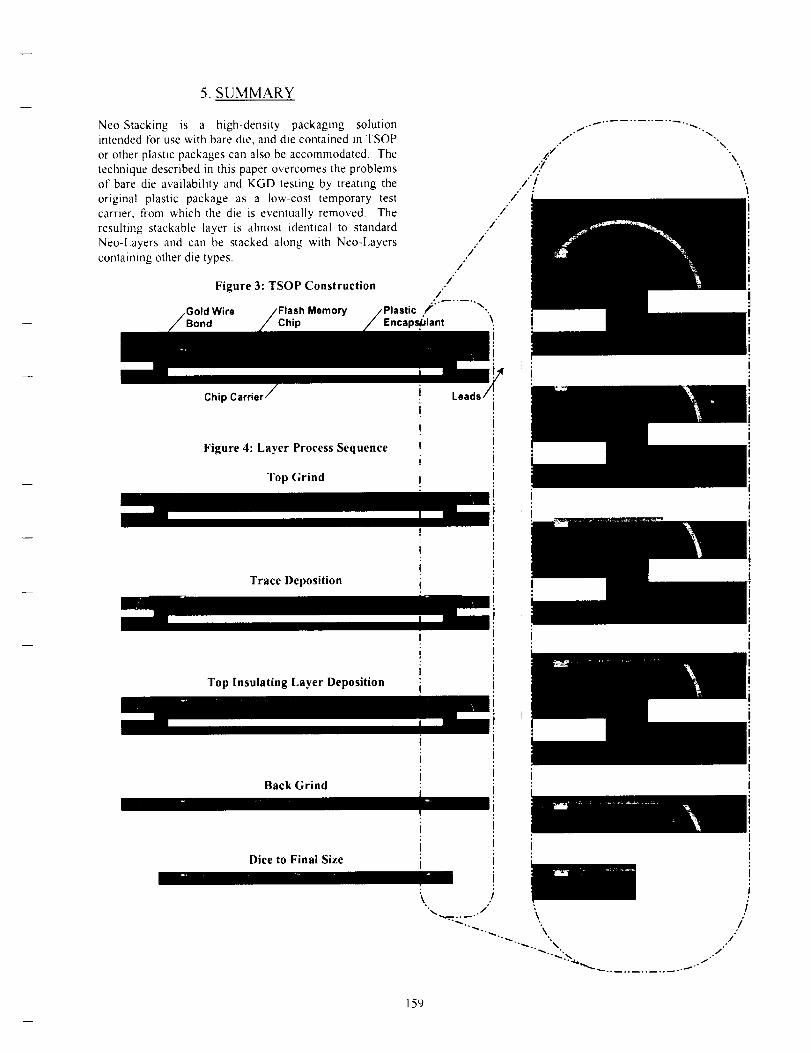
5.SUMMARY
Neo-Stacking is a high-density packaging solutionintended for use with bare die, and die contained in TSOP
or other plastic packages can also be accommodated. Thetechnique described in this paper overcomes the problemsof bare die availability and KGD testing by treating theoriginal plastic package as a low-cost temporary testcarrier, fi-om which the die is eventually removed, The
resuhing stackable layer is almost identical to standardNeo-I,ayers and can be stacked along with Neo-l,ayerscontaining other die types.
Figure 3: TSOP Construction
Wire
Encapsblant
/
/
o- _.
..f "\
.// ",
/:'/ \,,
/ i \i
Chip Carrier
Figure 4: Layer Process Sequence
Top Grind
Trace Deposition
Top Insulating Layer Deposition
Back Grind
Dice to Final Size
/\
•. ..._.. °_
-_.°•., J
"_-._._. .i •'
/
159

HIGH SPEED MRAM BUFFER FOR HIGH
CAPACITY NONVOLATILE SHOCK RECORDERS
R. Sinclair, R. Beech
NVE Corporation
11409 Valley View Road, Eden Prairie, MN 55344
bobsin(_nve.com, beech(_nve.com
Ahstract--[|igh shock data recorders require large
amounts of storage in order to capture high resolution
data. Also, high speed is needed in order to record pre-
trigger data. Nonvolatile storage is important in order to
prevent data loss. A system was developed with an 8
megabyte FLAStl and a PLD that contained a high speed
SRAM buffer memory. A new development in MRAM,
using SDT technology along with a unique circuit design,
is an ideal nonvolatile replacement for the SRAM. A new
film structure and circuit design yields a memory that
does not have disturb problems and that has the potential
of high production yields. The memory is high speed
(less than 10 nanosecond read or write), low power (less
than 30 Pico joule writes), has no wear out mechanism,
and is inherently RAD tlard, with STD cells tested to 1
Mrad.
TABLE OF CONTENTS
1. INTRODUCTION
2. HSDR MEMORY REQUIREMENTS
3_ MRAM BUFFER SOLUTION
4. NEW MRAM DEVELOPMENTS
5. MILITARY APPLICATIONS
6. CONCLUSIONS
7• ACKNOWLEDGMENTS
1. INTRODUCTION
Data recorders that measure fast, transient events require
large amounts of memory to achieve the resolutions re-
quired for wide bandwidths as well as fast buffer memory
to capture pre-tfigger events and buffer the slower
FLASH memory. This has been successfully accom-
plished in NVE's high shock data recorder (HSDR), for
Kirtland AFB. "[he HSDR contains both an 8 Megabyte
FLASH and a 256 byte, high speed buffer SRAM. The
SRAM contains a significant portion of the high-speed
shock event, and this data can be lost with battery failure
during that time• NVE has develop a low power,
nonvolatile MRAM, with Spin Dependent Tunneling
(SDT) technology, that can replace the current SRAM -
eliminating the volatility and power problems of the
SRAM. The MRAM is compatible with semiconductor
processing and can be easily inte grated into the
Programmable Logic Device (PLD) that is being used in
the HSDR design.
2. HSDR MEMORY REQUIREMENTS
Previous high shock data recorders have used battery
backed SRAM because of the recorders' high-speed re-
quirements. Problems of memory loss dunng battery
failure and high power consumption continue to be an
issue with this type of recorder. With the help of SBIR
funding from both Eglin AFB and Kirtland AFB, NVF,
desigmed an HSDR with the goal of resolving these issues.
The first issue has been addressed with the design of an 8-
channel recorder that contains 8 megabytes of FLASH
memory and a 256 byte SRAM buffer. The re corder is
contained on 2 printed circuit boards that assem ble to a
size of 0.3 x 1.1 x 2.5 inches, or about 1 cubic inch
volume. To facilitate manufacture and prototype testing,
the 2 circuit boards are built as a single board, that is latercut in half and stacked to form the final recorder
assembly. The recorder circuit board is shown, prior to
cutting and stacking, in Figures 2-1 and 2-2.
•. :-_:'_:?:_-:i_:_;_ :_
Figure 2-1. HSDR Assembly - Top View
Figure 2-2. HSDR Assembly Bottom View
160
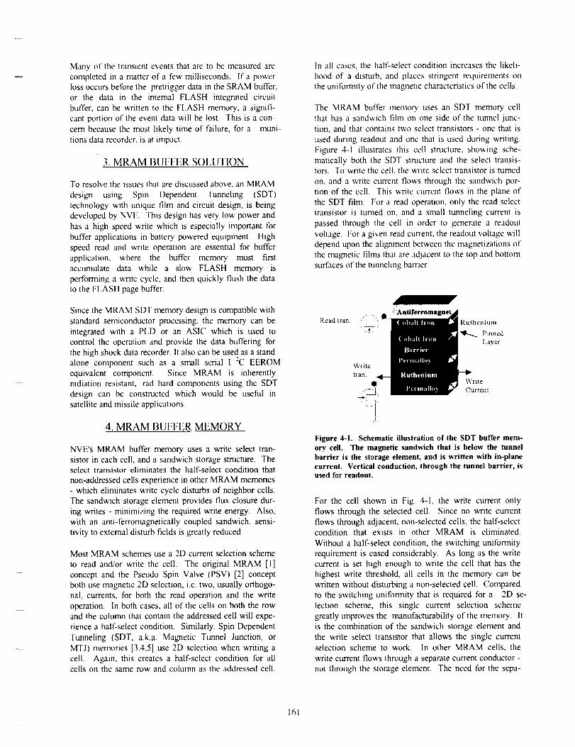
Manyofthetransienteventsthataretobemeasuredarecompletedinamatterofafewmilliseconds.If apowerlossoccursbeforethepretriggerdataintheSRAMbuffer,or thedatain the internalFI.ASHintegratedcircuitbuffer,canbewrittentotheFI.ASHmemory,asignifi-cantportionoftheeventdatawillbelost."[his is a con-
cem because the most likely time of failure, for a muni-
tions data recorder, is at impact.
3. MRAM BIJFFER SOLUTION
To resolve the issues that are discussed above, an MRAM
design using Spin Dependent Tunneling (SDT)
technology with unique film and circuit design, is being
developed by NVE This design has very low power and
has a high speed write which is especially important for
buffer applications in battery powered equipment. High
speed read and write operation are essential for buffer
application, where the buffer memory must first
accumulate data while a slow FLASH memory is
performing a write cycle, and then quickly flush the data
to the FI,ASH page bufl'er.
Since the MRAM SI)T memory design is compatible with
standard semiconductor processing, the memory can be
integrated with a PID or an ASIC which is used to
control the operation and provide the data buffering for
the high shock data recorder. It also can be used as a stand
alone component such as a small serial I :C EEROM
equivalent component. Since MRAM is inherently
radiation resistant, rad hard components using the SDT
design can be constructed which would be useful in
satellite and missile applications.
4. MRAM BUFFER MEMORY
NVE's MRAM buffer memory uses a write select tran-
sistor in each cell, and a sandwich storage structure. The
select transistor eliminates the half-select condition that
non-addressed cells experience in other MRAM memories
- which eliminates write cycle disturbs of neighbor cells.
The sandwich storage element provides flux closure dur-
ing writes - minimizing the required write energy. Also,
with an anti-ferromagnetically coupled sandwich, sensi-
tivity to external disturb fields is greatly reduced.
Most MRAM schemes use a 2D current selection scheme
to read and/or write the cell. The original MRAM [1]
concept and the Pseudo Spin Valve (PSV) [2] concept
both use magnetic 2D selection, i.e. two, usually orthogo-
hal, currents, for both the read operation and the write
operation. [n both cases, all of the cells on both the row
and the column that contain the addressed cell will expe-
rience a half-select condition. Similarly, Spin Dependent
Tunneling (SDT, a.k.a. Magnetic Tunnel Junction, or
MTJ) memories [3,4,5] use 2D selection when writing a
cell. Again, this creates a half-select condition for allcells on the same row and column as the addressed cell.
In all cases, tile half-select condition increases the likeli-
hood of a disturb, and places stringent requirements on
the uniformity of the magnetic characteristics of the cells.
The MRAM buffer memory uses an SDT memory cell
that has a sandwich film on one side of the tunnel junc-
tion, and that contains two select transistors - one that is
used during readout and one that is used during writing.
Figure 4-I illustrates this cell structure, showing sche-
matically both the SDT structure and the select transis-tors. To write the cell, the write select transistor is turned
on, and a write current flows through the sandwich por-
tion of the cell. This write current flows in the plane of
the SDT film For a read operation, only the read select
transistor is turned on, and a small tunneling current is
passed through the cell in order to generate a readout
voltage. For a given read current, the readout voltage will
depend upon the alignment between the magnetizations of
the magnetic films that are adjacent to the top and bottom
surfaces of the tunneling barrier.
Read tran Ru!lncnium
PinnedLayer
Writetran.
WrLte
Current
Figure 4-1. Schematic illuslralion of lhe SDT buffer mem-ory cell. The magnetic sandwich that is below the tunnelbarrier is the storage element, and is written with in-planecurrent. Vertical conduction, through the tunnel barrier, isused for readout.
For the cell shown in Fig. 4-1, the write current only
flows through the selected cell. Since no write current
flows through adjacent, non-selected cells, the half-selectcondition that exists in other MRAM is eliminated.
Without a half-select condition, the switching uniformity
requirement is eased considerably. As long as the write
current is set high enough to write the cell that has the
highest write threshold, all cells in the memory can be
written without disturbing a non-selected cell. Compared
to the switching uniformity that is required for a 2D se-
lection scheme, this single current selection scheme
greatly improves the manufacmrability of the memory. It
is the combination of the sandwich storage element and
the write select transistor that allows the single current
selection scheme to work. In other MRAM cells, the
write current flows through a separate current conductor -
not through the storage element. The need for the sepa-
161

rateconductor,combinedwiththesensitivityof otherMRAMdesignstodisturbfields,makesit impracticaltousethesinglecurrentselectionschemewiththeothertypesofMRAM.
l'he secondkeyfeatureof theinnovativeSI)'I buffermemoryis significantlylowerwritecurrentthanotherMRAMcells.Thislowerwritecurrentis dueto theclosedfluxswitchingbehaviorof theanti-ferromagneti-tallycoupledRutheniumsandwichfilmthatfomasthestorageelementintheSDTbuffercell.ConsiderfirstthewriteprocessinaPSVcell- whichisalsoasandwichfilmcell,butisnotanti-ferromagneticallycoupledandwhichiswrittenwithatippingfieldapplied.Figure4-2illustratesthePSVwriteprocess.The tipping filed is
assumed to be directed left to right in the figure The
combination of" the tipping field and the write current that
is flowing through the sandwich cause the magnetizations
of both layers to rotate in opposite directions - so that they
go through a paralleL alignment state This parallel
alignment greatly increases the internal demagnetization
fields, which leads to a comparatively large write current
requirement.
(a) (b)
........,, A
(c) (d)
Figure 4-2. Illustration of the switching process in a PSVcell: a) beginning rest slate, b) initial rotation due to tipping
field, c) rotation just past parallel, and d) final rest state.The parallel state, as the magnetizations rotate from (b) to(c), is a very. high energy state. Solid arrow shows magneti-zation of top magnetic film, dashed arrow shows magnetiza-tion of bottom magnetic fdm.
Now consider the switching process in the Ruthenium
(Ru) sandwich that is used for storage in the SDT buffer
cell. With a thin Ru layer, on the order of 10 A, the two
magnetic films are strongly coupled anti-parallel to each
other. As a write current is applied through the sandwich,
in a direction that generates fields that are opposing the
current direction of both the top and bottom magnetiza-
tions, the magnetizations begin to rotate - but stay anti-
parallel aligned. Because of the anti-parallel alignment,
demagnetization fields, and stray, fields, are minimized in
this sandwich - and remain at a minimum as the magneti-
zations rotate. This rotation process is illustrated in Fig.
4-3. In relatively wide sandwich structures, i.e. 2 _m,
write currents of 2.5 mA have been demonstrated. This is
significantly lower than the write requirements of other
MRAM cells ('ell switching times of under 3
been measured, which should allow nominal 10
times
(a) (b)
ns have
ns write
(c) (d)
Figure 4-3. Illustration of the switching process in Ru sand-
wich storage element that is used in the SDT buffer memo_"
cell: a) initial rest state, b) initial rotation after application ofwrite current, c) rotation over half way to new storage state,
d) final rest state. Solid arrow' shows magnetization of topmagnetic film, dashed arrow shows magnetization of bottommagnetic film.
Two different memory array architectures are envisioned
for the SDT buffer cell: 1) the I Junction per Cell (IJC)
architecture, and 2) the 2 Junction per Cell (2JC) archi-
tecture. As the name implies, the 1JC memory uses a
single SDT element for each cell, or bit, in the memory -
each junction is constructed with the Ru sandwich storage
element as shown in Fig. 4-1. Similarly, the 2JC memory
uses two SDT elements for each cell, with the two ele-
ments being written to opposite states during a write op-
eration
The IJC memory is denser than the 2JC memory, but has
slower readout than the 2JC memory. Fig. 4-4 shows,
schematically, the 1JC memory architecture. To write a
cell, the write driver is activated and the write select tran-
sistor for the addressed cell is turned on. The polarity of
the write current determines the written state of the cell.
A readout requires a reference, to compare with the read
voltage of the selected cell. During readout, the sense
current is activated and the read select transistor of the
addressed cell is turned on. Also, a 2X sense current is
activated, and flows through a reference cell. The refer-
ence cell consists of two SDT elements that are in parallel
and have been vent-ten to opposite states - so that the ref-
erence voltage will be halfway between the low and high
voltage of a single SDT element. Finally, a sense ampli-
fier is used to compare the memory cell voltage to the
reference voltage, and latch the result. Even with 40 mV
cell voltage differences - or about 20 mV difference be-
tween the cell voltage and the reference voltage, it is ex-
pected that the sense amplifier will require an auto-zero
step prior to readout. It is this amplifier requirement that
leads to somewhat slower readout speed for the IJC
memory relative to the 2JC memory.
162

i .---- "_ T --7-'-
Figure 4-4. Schematic diagram of the IJC memon' architec-lure. Readout requires that the read voltage of the selectedcell be compared with a global reference voltage.
The 2JC architecture uses a relatively simple latch cell
circuit with one SDT junction in each of the two halves of
the latch cell. This architecture is shown schematically in
Fig 4-5. The two SDT devices are written to opposite
states - one high resistance and one low resistance. To
read the memory, the latch is momentarily shorted, so that
both outputs are at the same potential, and then released.
When the short is removed, the different resistance that is
presented to the two halves of the latch, by the oppositely
written SDT junctions, causes the latch output to rapidly
drive to a known logic level based on which SDT.junction
is in a higher resistance state. This architecture is very
last and, for small arrays, has higher density than the IJC
architecture because of the lower overhead electronics.
The reason that this architecture has higher density for
small arrays is that the area that is required for overhead
circuitry, such as the sense amplifier, is much larger for
the l JC architecture than for the 2JC architecture. The
2JC architecture also has less stringent requirements on
SDT junction uniformity since the two SDT junctions
within a given cell act as local "references" for each other
- there is no need to match closely to a reference cell that
may be located a relatively large distance away. The
write operation in the 2JC architecture is the same as thatof the IJC architecture.
Figure 4-5. Schematic diagram of the 2JC memory architec-ture. The 2 SDT elements in each cell self-reference one
another for readout - requiring only a simple latch.
5. MILITARY APPLICATIONS
Although the basic concept of magnetoresistive random
access memory (MRAM) has led to working memory
cells on silicon and to limited numbers of working
MRAM chips, demonstration of practical manufacturabil-
ity of MRAM has not been reported One of the major
stumbling blocks to producing MRAM is the stnngent
magnetic uniformity requirement that the 2D memory
organization places on the MRAM cell, an organization
which all serious MRAM developments currently employ.
Staying with a 2D approach may delay or even preclude
the practical manufacturing of MRAM. Because defense
applications really need fast and truly nonvolatile random
access memories, this could represent a significant diffi-
culty for the Department of Defense. A Phase [ program
with Kirtland AFB entitled "Radiation-Hardened Non-
Volatile RAM" addressed the radiation resistance of
MRAM SDT cells and alternative circuit designs to
eliminate the problems of disturbs and uniformity found
in 2D MRAM memory architectures. Novel memory
cells and circuit architectures now make possible the de-
velopment of a reliable and manufacturable radiation hard
MRAM component that will satisfy the on-going need of
the military and space community.
Successful demonstration of the resistance of the SDI" cell
to radiation beyond I Mrad was completed during the
Phase I effort with Kirtland AFB. This demonstration has
established a firm foundation for the development of ra-
diation hard MRAM components. SDT junctions were
tested with survival beyond 1 Mrad without catastrophic
failures or large parameter shifts.
Applications for this new type of MRAM are not limited
to the HSDR buffer applications, but include military sat-
ellites and space-based weapon systems. Other applica-
tions would include systems that are required to function
163

in a nuclear battlefield environment, since this technologyis completely compatible with space qualified RAD HardCMOS processes such as those that are available fromPeregrine Semiconductor,
6. CONCLUSIONS
The development of new MRAM components, that usethe SDT cell and memory architecture that is presented inthis paper, will eliminate the problems of nonvolatility inshock recorders as well other applications that requiresmall, high speed, low power, random access memorydevices. In addition, with its inherent resistance to radia-
tion effects, these devices will be used in space and mis-sile applications. Initial devices with sizes on the order of
1 Kbyte will be developed, with sizes evolving up through16 megabit as production refinements are completed.Small buffer MRAM devices will be incorporated intoPIDs giving them high speed nonvolatile storage which isnot available today
7. ACKNOWI,EDGEMENTS
The authors wish to thank Dr James Daughton and DrAuthor Pohm for their contributions and innovations in
the development of these new memop0 cells
-[he authors would also like to acknowledge the supportof the following sponsors: DARPA (contract # F29601-00-C-0194), Air Force Advanced Research Laboratory atKirtland AFB (contracts # F29601-99-C-0032 and #F29601-01 -('-0121 )
8. REFERENCES
I J.Daughton, "Magnetoresistive MemoryTechnology", Thin Solid Films 216, p 162 (1992).
A. Pohm, J Anderson. R Beech, and J Daughton,"Bias Field and End Effects on the SwitchingThresholds of Pseudo Spin Valve Memory Cells",IEE Trans Magn 34, No. 4, p 3280 (1997).
P. Naji, M. Durlam, S. Tehrani, J. Calder, and MDeHerrera, "A 256kb 3.0V ITIMTJ Nonvolatile
Magnetoresistive RAM", ISSCC 2001 Proceedings(2001 )
R.E. Scheuerlein, W.J. Gallagher, S.S.P. Parkin, ALee, S. Ray, R. Robertazzi, W. Reohr, "A 10 ns read
and write non volatile memory array using amagnetic tunnel junction and FET switch in eachcell," 2000 IEEE International Solid State CircuitsConference. Digest of Technical Papers (Cat.No.00CH37056), 128 (2000).
5 J. Daughton, "Magnetic Tunneling Applied ToMemory", J. Appl. Phys. 81, No. 8, p 3758 (1997).
164

Design Hardness Techniques tbr Radiation Hardened Non-Volatile Memory
Presenter J Benedetto. UTMC Aeroflex
Material tbt this presentation was nol available at tile time ol'publlcation
165

SESSION #5: Emerging TechnologiesThursday, November 8, 2001
1:20 PM - 2:00 PM
Chair: S. Tyson, Air Force Research Laboratory
1:20 PM
1:40 PM
Future Development of Dense Ferroelectric Memories for Space
Applications; S. Philpy and G. Derbenwick, Celis Semiconductor
Corporation
Commercialization of 1T-Cell Ferroelectric Memories for Space
Applications; F. Gnadinger and G. Huebner, COVA Technologies Inc.,
G. Derbenwick and D. Kamp, Celis Semiconductor Corporation
166

-,. . /v/"_ - • ' '
j_ f,'
Future Development of Dense Ferroelectric Memories
for Space Applications
Stephen C Philpy and Gary F Derbenwick
('ells Semiconductor Corporation
5475 Mark Dab[ing Blvd., Suite 102
Colorado Springs, CO 80918
(719l 260-91 :;_; (719) 593-8540 {fax); steve(_celis-semi.com
Abstract--The availability of high density, radiation
tolerant nonvolatile memories is critical for space
applications. Ferroelectric memories, when fabricat-
ed with radiation hardened CMOS, can be manu-
factured and packaged to provide high density
replacements for Flash memory, which is not radia-
tion tolerant Previous work showed ferroelectric
memory cells to be resistant to SEU I_p and proton
irradiation [el, and ferroelectric storage capacitors to
be resistant to neutron exposure, tq In addition to
radiation hardness, the fast programming times,
virtually unlimited endurance, and low voltage, low
power operation make ferroelectric memories ideal
for space missions. Previously, a commercial, double
level metal 64-kilobit ferroelectric memory was
presented. TM Although the capabilities of radiation
hardened wafer fabrication facilities lag behind those
of the most modern commercial wafer fabrication
facilities, several paths to achieving radiation toler-
ant, dense ferroelectric memories are emerging. Both
short and long term solutions are presented in this
paper. Although worldwide major semiconductor
companies are introducing commercial ferroelectric
memories, funding limitations must be overcome to
proceed with the development of high density, radia-
tion tolerant ferroelectric memories.
TABI,E OF CONTENTS
I INTRODUCTION
2. FERROELECTRIC MEMORY
COMMERICIAI,IZATION
3 FRAM CHARACTERISTICS
4. SHORT TERM SOLUTIONS
5. LONG TERM SOLUTIONS
6 CONCLUSIONS
7 ACKNOWI,EDGEMENTS
8 REFERENCES
1. INTR()DU(71"ION
As global space communication systems advance and
as the requirements for NASA's deep space missions
become more challenging, thc need for radiation
tolerant computer systems with increased memory
capabilities are essential. "['he requirements for deep
space memory systems are survival in a radiation
environment of 1 Mrad total ionizing dose (T[D) or
more, operation for up to 10 years or more, and the
ability to be addressed by the spacecraft computer at
least twice every second for the purpose of storing
spacecraft state and epoch, or nearly a billion write
cycles. 151 These advanced computer systems will re-
quire large amounts of low power memory packed in
the limited area available onboard each spacecrat_
The use of nonvolatile memory in these systems
assures a spacecraft's ability to survive fauh condi-
tions and autonomously recover. 151 Current radiation
tolerant nonvolatile memories cannot meet all of the
requirements and are not dense enough to achieve the
limited area requirements.
In addition to ferroelectric memory, there are several
novel nonvolatile technologies in development that
potentially could meet the high density, low power,
and radiation tolerant requirements. These include
magneto-resistive, magnetic tunnel junction, and
chalcogenide glass memories. Taking into account
the present level of maturity of these technologies,
ferroelectric technology may provide the quickest
solution for the short term and an excellent solution
for the longer term.
Ferroelectric Random Access Memories (FeRAMs)
offer high radiation resistance, excellent retention,
virtually unlimited endurance, fast programming
times, and low voltage and low power opcration
compared to other types of conventional semicon-
ductor nonvolatile memories. FeRAMs are similar in
design and processing to stacked DRAMs, and
therefore may be well positioned to provide the high
density nonvolatile memories required for radiation
tolerant computer systems.
Although, at this time, there is no single manu-
facturer capable of producing high density radiation
tolerant ferroelectric memories that meet all of the
167

requirements,includinglowpower,therearcshortterm(3to5years)andlongtermsolutions(greaterthan5years)Thesesolutionsarediscussedinthispaper.
2. FERROEI.ECTRICMEMORYCOMMERCIAl IZATION
table I lists the semiconductor companies that have
produced commercial ferroelectric memories, in-
cluding some of the products manufactured
Table 1
Com a.l_!!E
FuJitsu
Matsushita
Ramtron
Rohm
Ferroelectric Commercialization
Product
Embedded 04k-bit ferroelectric
memory with microprocessor
I k-bit embedded ferroelectric
memory in RFID chip
4k-bit [:RAM,g, 16k-bit FRAM®,
64k-bit FRAM®. 256k-bit
FRAMg
16k-bit ferroelectric memory
In addition to the companies listed in Table 1, com-
panies pursuing ferroelectric memory development
are listed in Table 2. Not included are the numerous
university activities worldwide
Table 2. Major Ferroelectric Activities
Company Activity
tfitachi R&D
Hughes/Raytheon R&D
Hynix Prototype FeRAM
development
lnfineon/Toshiba Stacked 1T/IC 8M-bit and
64M-bit FeRAMs
Mitsubishi R&D
NEC Prototype embedded FeRAM
Ok i R&D
Samsung 4M-bit FeRAM R&D
Seiko Epson R&D
Sharp High density FeRAM R&D
Sony 1T R&D
STMicroeIectronics R&D consortium with IMEC
Texas Instruments R&D-high density Embedded
FeRAM at 0.18 / 0.13 micron
l'hc commercial market for ferroelectric memories
has been slow in developing because of problems in
fabricating high density ferroelectric memories on
aggressive silicon processing lines. Another reason
for the slow commercialization of FeRAMs may be
inadequate funding Dataquest estimated that by ear-
ly 1999. the FeRAM industry had spent less than
$500 million on research and development, whereas
the costs to develop a 1-Gbit DRAM might top $10billion. I_'1
Further compounding the problem of developing
ferroelectric memories for radiation tolerant applica-
tions is the small aerospace market compared with
the size of the market for commercial memories, and
the even smaller market within the aerospace market
for radiation hardened nonvolatile memory
3. (?()MMERCIAL FeRAM RADIATI()N
C! tARACrERISTICS
Although the ferroelectric device itself is radiation
tolerant, results of radiation testing of ferroelectric
memories by NASA and Brookhaven National Labs
indicate that most commercial FeRAM devices fail at
approximately 10 krads TID. Also, these comer-
cially available ferroelectric memories typically latch
up under relatively low heavy ion bombardment rl.
This is primarily due to the radiation softness of
commercial CMOS processes used to fabricate these
memories. Regarding neutron and proton irradiation,
it has been shown that ferroelectric memories should
be tolerant to neutron fluences up to 10 _5 neu-
trons/cm 2 and proton irradiation in excess of 10 _2
protons/cm 2 with no bit failures. I:_1 The authors are
not aware of any neutron or proton testing that has
been done regarding existing stand-alone ferroelectric
memories.
More advanced, commercial ferroelectric processes
are now becoming available that provide a higher tol-
erance to radiation, such as 25 krads for a Hynix 64k-
bit FeRAM tested by JPL. However, these levels are
still too low to avoid significant spacecraft radiation
shielding.
4. SttORTTERM SOLUTIONS
To develop a solution for JPL/NASA regarding a low
density ( 1M-bit) radiation tolerant nonvolatile mem-
ory, Celis Semiconductor started a program in 1998
to provide a 1M-bit FeRAM using a split wafer fabri-
cation process. This design was to use radiation
hardened CMOS underlayer wafers processed at
Sandia National Laboratories and ferroelectric
168
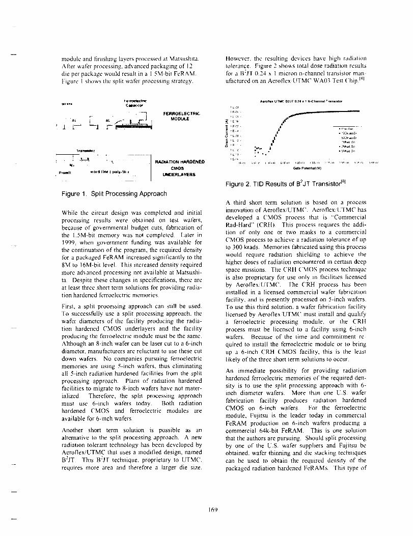
moduleandfinishinglayersprocessedatMatsushita.Afterwaferprocessing,advancedpackagingof"12dieperpackagewouldresultinat.5M-bitFeRAM.Figure1showsthesplitwaferprocessingstrategy.
However,theresultingdeviceshavehighradiationtolerance.Figure2showstotaldoseradiationresuhsforaB2JT0.24x 1micronn-channeltransistorman-ufacturedonanAeroflex/UTMCWA03TestChip.I<
' J L--* . •
FERROELECTR_C
MODULE
"lr|_¢
i P,..,_wll ,_of_ llt_! I POlI-_I I...... I.Im_E!_I.AYIE R S
Figure 1. Split Processing Approach
While the circuit design was completed and initial
processing results were obtained on test wafers,
because of governmental budget cuts, fabrication of
the 1.5M-bit memory was not completed. Later in
1999, when government funding was available for
the continuation of the program, the required density
{'or a packaged FeRAM increased significantly to the
8M to 16M-bit level. This increased density required
more advanced processing not available at Matsushi-
ta, Despite these changes in specifications, there are
at least three short term solutions for providing radia-
tion hardened ferroelectric memories.
First, a split processing approach can still be used.
To successfully use a split processing approach, the
wafer diameters of the facility producing the radia-
tion hardened CMOS underlayers and the facility
producing the ferroelectric module must be the same.
Although an 8-inch wafer can be laser cut to a &inch
diameter, manufacturers are reluctant to use these cut
down wafers. No companies pursuing ferroelectric
memories are using 5-inch wafers, thus eliminating
all 5-inch radiation hardened facilities from the split
processing approach. Plans of radiation hardened
facilities to migrate to 8-inch wafers have not mater-
ialized. Therefore, the split processing approach
must use &inch wafers today. Both radiation
hardened CMOS and ferroelectric modules are
available for &inch wafers.
Another short term solution is possible as an
alternative to the split processing approach. A new
radiation tolerant technology has been developed by
Aeroflex/UTMC that uses a modified design, named
B2jT. This B2jT technique, proprietary to UTMC,
requires more area and therefore a larger die size.
Tk03
=.Oa -
_k05 -
_" ,E06.
E _E 10.
t_. 12.
_E13-
1__.14.
Aeroflex UTMC B2JT 0.24 _, t N-Channel Transistor
,ff$ ",3C_a_mS'
ib0_raolS!'
Io_ _ ,2MradlSih
Gito Potential (V)
Figure 2. TID Results of B2JT Transistor ["l
A third short term solution is based on a process
innovation of Aeroflex/U'lMC. Aeroflex/UTMC has
developed a CMOS process that is "Commercial
Rad-Hard'" (CRH). This process requires the addi-
tion of only one or two masks to a commercial
CMOS process to achieve a radiation tolerance of up
to 300 krads. Memories fabricated using this process
would require radiation shielding to achieve the
higher doses of radiation encountered in certain deep
space missions. The CRH CMOS process technique
is also proprietary for use only in facilities licensed
by Aeroflex/UTMC The CRH process has been
installed in a licensed commercial wafer fabrication
facility, and is presently processed on 5-inch wafers.
To use this third solution, a wafer fabrication facility
licensed by Aeroflex/UTMC must install and qualify
a ferroelectric processing module, or the CRH
process must be licensed to a facility using &inch
wafers. Because of the time and commitment re-
quired to install the ferroelectric module or to bring
up a 6-inch CRH CMOS facility, this is the least
likely of the three short term solutions to occur.
An immediate possibility for providing radiation
hardened ferroelectric memories of the required den-
sity is to use the split processing approach with 6-
inch diameter wafers. More than one US. wafer
fabrication facility produces radiation hardened
CMOS on 6-inch wafers. For the ferroelectric
module, Fujitsu is the leader today in commercial
FeRAM production on 6-inch wafers producing a
commercial 64k-bit FeRAM. This is one solution
that the authors are pursuing. Should split processing
by one of the U.S. wafer suppliers and Fujitsu be
obtained, wafer thinning and die stacking techniques
can be used to obtain the required density of the
packaged radiation hardened FeRAMs. This type of
169

advanced packaging not only improves density, butalso reduces weight, critical ['or space missions.
5. L()NG TERM SOLUTIONS
Greater than 5 years from now, solutions for radiation
tolerant nonvolatile memory, may come fromalternative new semiconductor technologies indevelopment today. These technologies include ad-vanced ferroelectric memories using a single ferro-electric transistor (IT) memory cell, chalcogenideamorphous glass memories, magneto-resistive mem-ories, and magnetic tunnel junction memories, amongothers. While all these technologies can be maderadiation tolerant, each approach has its uniqueadvantages and disadvantages
A new ferroelectric memory technology is being
developed that can provide a long term solution fordense radiation hardened non-volatile memory for
space missions. This advanced ferroelectric tech-nology uses a ferroelectric transistor for the storageelement instead of a ferroelectric capacitor. Thememory cell size would be smaller than a DRAM
memory cell and comparable to a Flash memory cell,with all of the favorable electrical and radiation
characteristics of ferroelectric memory. Furthermore,the memory architecture provides for non-destructiveread out, as compared to the destructive, DRAM-typeread out of one-transistor, one-capacitor (IT/IC)ferroelectric memories currently in development.
Cells Semiconductor and COVA Technologies arejointly developing a ferroelectric memory using a 1Tmemory cell. A cross section of the IT memorystorage element is shown in Figure 3. Comparison ofthis new memory cell size to other semiconductormemory cell types is shown in Table 3. Memorysizes comparable to those of Flash memory andsmaller than those of DRAMs may be obtainable.
Ease of manufacturing is a primary goal of tileCOVA/CeIis advanced ferroelectric technology pro-gram. The memory cell is expected to integrate withCMOS more efficiently than a 1T/IC ferroelectricmemory cell. Because of the ease of manufacturing,the production of dense radiation hardened ferro-electric memories by United States fabricators may
become a reality
The COVAJCelis ferroelectric memory technology,when mature, may eliminate the use of DRAMs.Because this new technology may replace bothDRAM and Flash memories, this new technology
may be more readily embraced by semiconductorcompanies to the point where it will receive the levelsof R&D funding and efforts necessary to bring it intothe mainstream.
Table 3. Comparison of Memory Cell Sizes.
Memory Cell Type Cell Size (Fe)
SRAM 50 - 100DRAM 7 - 12Flash 5 - 12
DRO FeRAM (IT/1C) 25 - 75
NDRO FeRAM (1Y) 5 - 6
6. CONCLUSIONS
The development of a radiation tolerant ferroelectricmemories using split wafer processing methods anddie stacking can provide a short term solution to meetthe needs of today's aerospace marketplace. I,ongerterm, a new ferroelectric technology using singletransistor ferroelectric memory cells that is in de-
velopment may provide very high density nonvolatilememories with non-destructive read out capabilitiesfor the aerospace marketplace
Ferroelecmc Gate D_electnc
Soulce
Gate
Polanzalion
Dram
(l_annel
ISubstrare
Figure 3. 1T Ferroelectric Memory Cell
7. ACKNOWI,EDGEMENTS
The previous split process FeRAM development
program described in this paper was funded under apurchase order from the Jet Propulsion Laboratory,California Institute of Technology The authorsexpress their appreciation to the Jet PropulsionLaboratory, Sandia National Laboratories andMatsushita for their support of that program. Theauthors appreciate their numerous discussions andinteractions with Jet Propulsion I,aboratory, SandiaNational Laboratory, Aeroflex/UTMC and IrvineSensors personnel
170

8. REFERENCES
IIIj. M. Benedetto, G. F. Derbenwick and J D. Cuchi-
aro. "'Single Event Upset Immunity of Strontium
Bismuth Tantalate Ferroelectric Memories," IEEE
1)'ansa_'tions on Ntu'lear S,'ie,_ce ( 1999 ).
I-'lMeasurements perlbrmed by Gary Swift of the Jet
Propulsion Iaboratory in 1999.
I_IR. A. Moore, J. M. Benedetto, J. M. McGarrity and
F. B. McLean. "'Neutron Irradiation Effects on PZT
Ihm Films for Nonvolatile Memory Applications,"
IEEE Tram Nucl. Sci. NS-3& 1078-1082 (1991).IqS. S. I_ee, N S. Kang, S. C. Philpy and G. F Der-
benwick, "'Reliability and Performance of a 64K
Fcrroclectric Memory," 2000 IEEE Microelectronics
Reliability and Qual(/ication Works'hop, Glendale,
CA: Oct 31 Nov. 1; Session V.3.
ISlK. F. Strauss and Y. Daud, "'Overview of Radiation
Tolerant Unlimited Write Cycle Non-Volatile Mem-
ory," Proc. ()/the 2000 IEEE Aero.v)ace ('rml_,rence,
Big Sky, MT, March 19-25, 2000.
I(,Ij. Handy, "Where do ferroelectrics fit'?," Data-
quest, Feb 1, 1999 and EDN, "'Exotic memories,
diverse approaches, April 26, 2001.
171programmable Technologies Web Site, "A scien-
tific study of the problems of digital engineering for
space flight systems, with a view to their practical
solution. Memories Some Radiation Test Results,"
http//klahv org/m emories, htm (200 l ).
I8IBeJT Test results courtesy of Aeroflex/UTMC,
Colorado Springs, CO.
About the Author
Stephen Philpy is a founder of Celis Semiconductor
Corporation. ife previously worked for Mostek and
UTMC, developers of semiconductor memories and
radiation hardened ASICs. He is also a founder of
Symetrix Corporation, a developer of ferroelectric
materials. He has been involved in the ferroelectrics
industry since 1988. fie has a BS in Electronics
Engineering from Texas A&M University and an
MBA from the University of Colorado.
171
• '[_'
/f .) .L
C.'-'
Commercialization of 1T-Cell Ferroelectric
Memories for Space Applications
Fred P Gnadinger and Gregory G lfuebner
COVA Technologies lnc
2860 South Circle Drvce, Suite 2323
Colorado Springs, CO 80906
(719) 538-9030. (719) 540-8855 (fax): fred@covatech cornand
Gary. F Derbenwick and David A Kamp
(?ells Semiconductor, 5475 Mark Dabling Bird, Suite 102
Colorado Springs. CO 80918
(7191 260-9133, (719) 593-8540 (faxL dave@cells-semi corn
Abstract -- A new class of ferroelectrlc materials Is
under development with parameters ideally suited for 1T
cell technology enabling low voltage operation with im-
proved retenuon This paper describes the approach taken
to integrate the ferroelectric IT cell module into a CMOS
plocess with special emphasis on iadiation hardness for
space applications
q ABI,F OF' CONIENI S
I Introduction
2 Propertms of the New Ferroelectnc Material
3 Integration of the Ferroelectrlc Transistol
Module
4 Summa_
5 Biography
1. Introduction
Standard ferroe[ectrlc nonvolatile memories have re-
lauvely large memory cell sizes, leading to high manu-
facturing costs A 1- transistor (1T) memory, cell reduces
the area reqmrements considerably rendering ferroelectrlc
memories cost competmve The ferroelecmc materml _s
deposited directly on silicon with a buffer layer in bet-
ween silicon and ferroelectnc This interracial oxide layer
is desirable to provide a stable interface Commonly used
ferroelectrlc materials have relatively high dielectric per-
mlttlwty so that most of the apphed voltage drops over
this interfacial layer making low voltage operation diffi-
cult Another challenge in a IT cell is to achieve adequate
data retenUon, which is negatively impacted by the depo-
larization field, mobile ionic charges and charge InjecUon
A new class of ferroelecmc materials is under deve-
lopment with parameters ideally suited for 1T cell tech-
nology enabling low voltage operauon with improved
retention The material is deposited by MOCVD usmg
hqmd precursor injection Into a flash evaporator
In order tbr ferroelectrlc memories to become mare-
stream, in addition to a competmve cell s_ze. other manu-
facturing challenges have to be met The most _mportant
one _s the integration of the ferroelectrtc module into a
manufacturing process (eg CMOS) m a cost effective
and technically reliable manner This paper describes the
potential CMOS integration approaches with special em-
phasis on preserving the radmUon hardness of the process
for space applicauons
2. Properties of the new ferroelectric material
Table ! hsts the typical parameters we have achieved,
measured on a Metal-Ferroelectric-Oxide-Semiconductor
(MFOS) capacitor Figure I shows a Wpical CV plot The
arrows m Figure 1 m&cate the direction the hysteresis
loop is traversed For n-Wpe slhcon a counter clockwise
direcuon ts consistent with ferroelecmc switching and
dlstmgmshes ferroelecmc switching from charge injection
at the silicon interface
The most _mportant characterlsUcs of the new mate-
rtal are the low dielectric permlttlW W (e_ _ 10) and the
high transmon temperature (>700 °C) A low _ enables
low voltage operauon and, indirectly, improves retentmn,
whereas a high transmon temperature is important for cost
effectwe and reliable integration of the ferroelectric
transistor module into CMOS The mtegrauon challenges
will be decrtbed in more detail in the next section
3. Integration of the ferroelectric transistormodule
Since the new ferroelectric material is a high tem-
peratttre material with a transmon temperature (Curie
temperature) of greater then 700 "C (see Table I) the
172
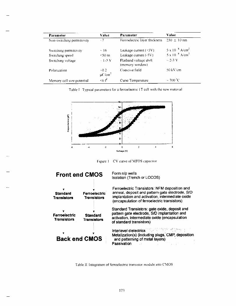
Parameter Value Parameter Value
Non-switching perrnltu,;lty - 7 Ferroelectnc layer thickness
Switching permtttp_lty - 16
Switching speed <50 ns
Switching voltage --1-3 V
Polarization
Memoir' cell s_ze potenhal
-02
_tC/cm 2
<6 f2
Leakage current ( _5V)
Leakage current (-5V)
Flatband vohage shift
(memo_' window)
Coercive field
Curie Temperature
230 _+ l0 nm
5x10 8A/cm:
5 x 10 8 A/cm 2
-- 2-3 V
50 kV/cm
- 700 °C
Table I Typical parameters for a ferroelectnc I T cell with the new material
o
-6 -4 -2
Figure 1
111
14
0
Voltage (V)
2 4
CV curve of MFOS capacitor
Front end CMOS
i,F T
Standard Ferroelectric
Transistors Transistors
Ferroelectric StandardTransistors Transistors
Back end CMOS
Form nip wells
Isolation (Trench or LOCOS)
Ferroelectric Transistors: NFM deposition and
anneal, deposit and pattem gate electrode, S/D
implantation and activation, intermediate oxide
(encapsulation of ferroelectric transistors)
Standard Transistors: gate oxide, deposit andpattern gate electrode, S/D implantation andactivation, intermediate oxide (encapsulationof standard transistors)
Interlevel dielectrics : , ,:: :: :ii: ::! i:3 ::: -Metalization(s) (including plugs; CMP, depositionand patterning of metal layers)
Passivation
Table II Integranon of fevroelectric transistor module into CMOS
173

ferroelectric transistor module can be integrated
into a standard CMOS flow early in the process
The ferroelectnc transistors can be formed either
before or after the f_ormation of" the standard
transistors as described m Table 1[
The new material has high vapor pressure so
that the probability that volatile species could be
transported from one part of a wa(er to another
and introduce contaminants Is low
In order to avoid even th,s small probabdl_
of contammanon, the ferroelectnc transistors can
Ferro transistors oriorto standard transistors
1 Form nip wells
2 Isolation (trench or LOCOS)
3 Form ferToelectric bansistors (NFM
deposition and anneal, deposit and patterngate electrode, S/D implantation and
activation)
4 Intermediate oxide (encapsulation of ferrotransistors)
5 Form standard transistors (gate oxide,
deposit and pattern gate electrode, oxide
spacers, S/D implantation and activation)
6. Intermediate oxide (encapsulation of
standard transistor)
7. Interlevel dielectrics
8. Metalization(s) (including plugs, CMP,
deposition and patterning of metal layers)
9 Passivation
be encapsulated with a protecnve layer if they
are formed prior to the standard transistors, or
the standard transistors can be encapsulated if
they are formed first For maximum protection
both types of transistors can be encapsulated
Figure 3 shows a cross section of a ferroelectnc
transistor integrated into a one- poly, three-
metal layer CMOS process In this implemen-
tation the ferroelectric transistor is formed prior
to the standard CMOS transistors and en-
capsulated with a thin oxide layer deposited with
MOCVD
Ferro transistors afterstandard transistors
1 Form nip wells
2 Isolation (trench or LOCOS)
3 Form standard transistors (gate oxide,
deposit and pattern gate electrode, oxidespacers, S/D implantation and activation)
4 Intermediate oxide (encapsulation of
standard transistors)
5 Form ferroelectric transistors (NFM
deposition and anneal, deposit and patterngate electrode, S/D implantation and
activation)
6. Intermediate oxide (encapsulation of ferro
transistor)
7 Interlevel dielectrics
8 Metalization(s) (including plugs, CMP,deposition and patterning of metal layers)
9. Passivation
Table 111 Process Integration of fe_oelectnc transistor
Contact
Plugs
Standard NFMTransistor Ferr0electdc
Encapsulated Transistor
immmmmt.... Metal3
-_}_m_-_..-.-_._,_ _._ Metal2
Interle_l(lielectdc Encapsulatior
layer
\
Gate SourceyDrain Standaed Ferroelec_c Source/Drain NFMoxide b'ansistor transistor (ferroelectnc
gate gate layer)
Figure 3 (;ross secnon of standard transistor and ferroelectric transistor integrated
into one- !0oN, three- metal CMOS process
174

fable 111 is a brief process flow for these
two main variations of integration The high
processing temperature of our new material of
approximately 850 °C, which would be unaccep-
table for a standard 1TIC cell technolog, y, ls an
advantage for the integration of a ferroelectric
transistor It allows high temperature CMOS pro-
cesslng steps such as iunctlon activation, poly-
slhcon deposition and doping to be performed
after the formation of the ferroelectrlc transistors
Depending on the thermal budget of the CMOS
process certain steps could be combined in order
to s_mpll6/ processing Examples are jtmcnon
activation of both standard and ferroelectric
transistors
4 Summa_
ferroelectrlc transistor module based on a
new ferroelectri¢ material is under development
In addmon to having a low dielectric permlttl,/1D'
enabling low voltage operation and optimum
interface ptopernes, the new material has a high
transmon temperature (Curie temperature)
Facilitating integration into CMOS The material
can v,'_thstand the processing temperatures
accoclated with polysihcon deposltmn, junction
activation and so on, The ferroelectric module
can be integrated enher before or after the
flmnation of the standard transistors
The ferroelectrlc transistors can be
encapsulated with an oxide layer preventing any
potential contaminants to escape No majol
modifications to the CMOS process are required
The ferroelectnc transistor, due to the ionic
rather than electronic storage mechanism, is in-
herently radiation hard The proposed integration
will preserve the radiation hardness of the
CMOS process and we expect the ultimate
radianon performance to be limited by the
radiation hardness of the tmderlying CMOS
process
5. Biography
Dr Fred P Gnadinger is President and CEO
of COVA Technologies, lnc a semiconductor
fabrication eqmpment company in the field of
liquid injection - and flash evaporation systems
for complex oxide deposition systems based on
MOCVD Prior to COVA he was President and
CEO of Microtromx Corporation, a company he
founded in 1990 to develop ferroelectnc tech-
nology and products for nonvolatile memories
Dr Gnadmger Is the prior Chief Operating
Officer and Chief Technical Officer of Ramtron
Corporation, a pubhc semiconductor company
engaged m the development of semiconductor
memories based on ferroelectric technolog, y
Dr Gnadmger holds a Ph D degree m
Electrical Engmeerlng from the Unlversl_' of
Kansas l,awrence. Kansas, and an MSEE degree
from the Swiss Federal lnsutute of Technology
(ETH), Zurich, Switzerland Dr Gnadtnger holds
6 US Patents and several foreign Patents and has
numerous pubhcatlons including a book chapter
pubhshed by Academic Press, New York He has
also given many talks at Scientific Conferences
and has been an invited speakeJ on several
occasions
175
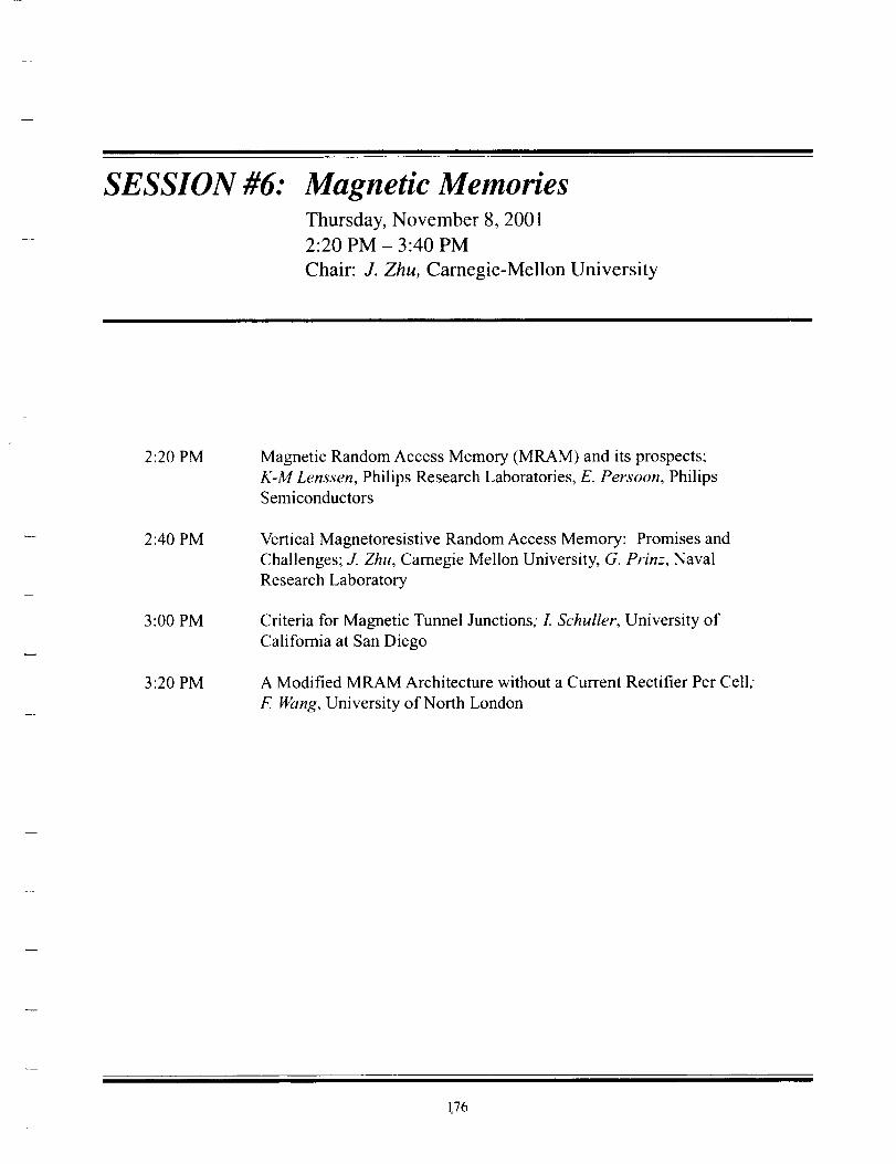
SESSION #6: Magnetic MemoriesThursday, November 8, 2001
2:20 PM - 3:40 PM
Chair: J. Zhu, Carnegie-Mellon University
2:20 PM
2:40 PM
3:00 PM
3:20 PM
Magnetic Random Access Memory (MRAM) and its prospects;
K-M Lenssen, Philips Research Laboratories, E. Persoon, PhilipsSemiconductors
Vertical Magnetoresistive Random Access Memory: Promises and
Challenges; J. Zhu, Carnegie Mellon University, G. Prinz, Naval
Research Laboratory
Criteria for Magnetic Tunnel Junctions; I. Schuller, University of
California at San Diego
A Modified MRAM Architecture without a Current Rectifier Per Cell;
F. Wang, University of North London
176

/"/ r -J _ '
Magnetic Random Access Memory (MRAM)
and its prospects
K.-M.H. Lenssen
Phi lips Research laboratories, Prof. Ilolstlaan 4, N1_-5656 AA Eindhoven, The Netherlands,
+3 I-4(I-2742754, kars-michiel.lenssenf_?philips.com
E.H.J. Persoon
Philips Semiconductors, Building BF-107, P.O. Box 218, NI .-5600 MI) l'indhoven
+31-40-2724075, eric.persoon!_/philips.com
Abs4aract--Recently the R&D activities concerning
Magnetic Random Access Memory' (MRAM) have shown
an acceleration. Commercial MRAM products are
planned to enter the market as early as 2004. In this paper
first an overview will be given of the recent developments
and the present status of MRAM. Potential issues (like
thermal stability, magnetic shielding) will be discussed
and some ideas for improvements will be proposed. Inorder to obtain indications for the most attractive MRAM
application areas, the total (multi-billion-dollar) memory
market can bc divided in three segments: embedded
memory, companion memory' and removable memory,
diftirring in the percentage of the chip area that is
occupied by memory. In each of these segments MRAM
will have to compete with different types of conventional
memory (that form the present solutions) and therefore
will also have to meet different specifications. It is likely
that two variants of MRAM will be developed: a high-
performance version (with fast read and write) and a low-
cost MRAM (with high density) to target the differentmarket needs.
TABI,E OF CONTENTS
1. INTRODUCTION
2. PRFSFNT STATUS OF MRAM
3. SOME POTENTIAL TECHNICAL ISSUES
4. COMPARISON WITH OTHER MEMORY TYPES
5. MEMORY MARKET SEGMENTS
6. CONCI,USIONS
7. ACKNOWLEDGMENTS
1. INTRODUCTION
An MRAM is a memory (I) in which the stored data are
represented by magnetization directions and (2) in which
the read-out is done by a resistance meast, rement (for a
recent overview about MRAM see, for example, Refs.
[1,2,3]). This definition implies that its operation relies on
a magnetoresistance phenomenon. Early MRAMs based
on the anisotropic magnetoresistance (AMR) effect _,,ere
limited in their use mainly to military, and space
applications, since the amplitude of the AMR effect in
thin fihns is typically less than 5%.
The discover), in 1988 of the giant magnetoresistance
(GMR) effect [4] and a breakthrough in the field of
magnetic tunnel junctions around 1995 [5] improved the
perspectives of MRAM and enabled, in principle, the
realization of MRAMs for general applications. Tunnel
magnetoresistance (TMR) effects with amplitudes up to
>50% have been shown, but because of the strong bias-
voltage dependence, the useable resistance change in
practical applications is at present around 30%. While the
GMR effect is already applied in commercial products
like HDD read heads [6] and magnetic sensors [7], this is
not yet the case lbr magnetic tunnel junctions.
In general, both GMR and TMR result in a low resistance
if the magnetization directions in the multilayer are
parallel, and in a high resistance when the magnetizations
are oriented antiparallel.
The addressing of the MRAM is done by means of anarray of crossing lines. Writing a certain cell is equivalent
to setting a magnetization in the desired direction (for
example, magnetization to the lett means '0' and
magnetization to the right means '1'). By applying a
current pulse to a bit line and a word line a magnetic field
pulse is induced. Only the MRAM cell at the crossing
point of both lines experiences the maximum magnetic
field (i.e. the vectorial addition of the fields induced by
both current pulses) and its magnetization is reversed; all
other MRAM cells below the bit or word line are exposed
to the significant lower feld that is caused by a single
current pt, lse and will theretbre not change their
magnetization directions.
The read-out method depends on the type of MRAM. In
the case of exchange-biased magnetic tunnel junctions
177

witha fixed magnetization direction the data are stored in
the other, tree magnetic layer, which of course should not
be disturbed b) the read-out. [n this case the absolute
resistance of the cell is measured (if desired, differentially
with respect to a reference cell). This cell is selected by
¢neans of a switching elernen! (usually a transistor), which
implies that in this case one transistor is required per cell.
2. PRESENT STATUS OF MRAM
In the last )ear the R&I) activities concerning MRAMhave shown an acceleration [n l)ecember 2000 IBM and
Infineon announced a cooperation on MRAM
developrnen! [8,9]. It was stated thai MRAM products
would be commercially available already in 2004; this
would relate to 128 Mb or 256 Mb memories in 0.13 tam
technology. This timing corresponds to the planning of
Motorola who announced samples in 2003 and volume
production in 2004. In Jtme 2001 [10] it was even stated
that volume production would be only 1.5 year away as
Motorola and IBM speed up their development work.
Also major progress has been made in the field of MRAM
demonstrators: at the ISSCC2001 Motorola presented a
complete 256kb MRAM chip in 0.6 tam technology [11],
[n the meantime USTC very recently claimed thedemonstration of the first commercial MRAM on their
website [12], although samples are not yet available.While most others concentrate on TMR, USTC uses the
GMR effect in their MRAIVl.
Other industrial companies active in MRAM research and
development include Hewlett-Packard, NVE, Toshiba,
NEC, Samsung, Read-Rite and Philips.
[n the field of more fundamental research a breakthrough
was the observation of 96% spin polarization in a half-
metallic ferromagnetic material (a single-crystal film of
CrO2) [13,14]. Although it is still unclear whether it will
be easily possible to implement this material in MRAM,
this opens up perspectives for significantly larger
magnetoresistance ratios in future MRAMs.
3. SOME POTENTIAL TECHNICAL ISSUES
In our previous overview [3] we identified already several
possible issues or weaknesses of MRAM. In the followingsome issues will be discussed and some solutions will be
proposed without aiming at completeness.
* ('ell size
As we pointed out already earlier, the cell size is
mainly determined by the metal line width that is
required because of the current pulses; therefore, the
use of copper metallization enables much smallercells. In the demonstrator of Motorola cell sizes of
20F: (with F being the smallest feature size) were
already obtained, which is indeed smaller than the
size thal we had calculated for 0.18 tam technology
with TiW/AI metallization [3].
Temperature stabilio'
CMOS processes usuall) include an anneal step at or
above 400°C. Considering our experiences on the
thermal stability of GMR sensors [15] this seems tobe a serious issue fur embedded memories, if one
wants to adhere to the standard CMOS process.
Resistance and scalmgThe resistance of GMR elements is so small that one
can wonder if the 5 can be used to realize MRAM
memories that can compete with Flash.
In principle there are two possibilities:
I. if one connects several (let's say: N) GMR
elements in series in order to increase the total
resistance, the magnetoresistance efl;_'ct is
divided by the number N. That means a nett
resistance change of _1% or less (e.g. 16elements with 8% GMR effect results in 0.5%
resistance change); this means a signal change to
be detected of only several mV's (since the
resistance per square is around 15 f2and an
element will comprise a few squares). That is
probably too small to realize easily in a reliable
low-power and cost-effective way.
2 if one switching element is used per GMRelement, one has indeed the whole GMR effect
(e.g. 8% resistance change) available to detect,
but the difference in resistance between a single
GMR element and a transistor is so large, that
that it is difficult to measure the resistance
change in an efficient wa_. That wotfld mean that
either one has to measure tbr a long time, or a so
complicated read-out method is needed that the
total cell area becomes too large.
Theretbre we believe that TMR is more promising tbr
MRAM than GMR at this moment.
It should be noted that tbr TMR the scaling of the
resistivity (which depends on the thickness of the
ttmnel-barrier layer) is crucial in order to be able to
follow Moore's law. With the present status this
seems however already possible fbr at least three
generations. After that, new tunnel barriers with a
lower energy barrier ma3, allow further scaling.
Thermal relaxation
If magnetic elements become very small, their
magnetizations can switch spontaneously. In the
following we will discuss, using simple estimations.
in what range of dimensions limits due to this so-
called superparamagnetic effect might be expected.
178

wq
r(
17J
l"igur_ I Sch_'m¢_tic vicar _?/¢1magnetil element ¢lnd}krile conduclor
Consider a magnetic element with width d, length .vd
and thickness _t (Figure I) Then the volt, me V is
(i) V-_d "_
A current / in a conductor with width _ that is close to
the elemenl induces a write field H.
For thermal stability at a temperature 7" it is requiredthat
(2) (Koj_t3/(k_T)_> R.
with the ratio R for example 50 2.
The effective anisotropy constant K,t_ is given by
(3) K:n= H Po M_/2
(in which M_ is the saturation magnetization) and so it
fbllows that the general condition fbr thermal stability
is
(4) (H _to M,V)/(2k_T)_> R.
This is comparable to the condition mentioned in [.2].
A first, very simple estimation is the following. If thewrite conductor with width w is close to the element
(i.e. on a distance much smaller than w) the current /
induces a write field:
(5) H-L,'(2w).
The combination of equations (l), (5) and (4) leads tothe condition:
(6) (ltlo M_ tx _)/(4wk_T) > R
or. with _=xd,
(7) d >_(4k_TR)/(l _lo M_ t)
' The relevant(hickncss has to Ix:t_en, for example the thickness of themaL-'neticlayer in which the data are stored' The choice of the vaLuemay depend on the cnvironment and thercquir_ life time
With t=6 nm, x-4, M_-1.4 MA,'m (value t_)r e.g. Co-
Fe), T=350K, /=1 mA, R=50, _=47T10Vlt.'m and
kl_=1.3807.10 -'_ J'K this results, for example, in:
(8) d>9_nm.
It has to be noted that in general dwill be larger than
the smallest feature F of a technology node; so. for
example, in a 50 mn technology,,, d will probably still
be at least 100 nm. It has implicitl_ been assumedthai the distance between the write conductor and the
magnetic elemen! is significantly smaller than w.
This estimation is oversimplified, bul it alread?
indicates that the theoretical limits are around the
technology nodes of interest for MRAM (50-100
nm)The exact relation between I and H can also be left
undefined. In that case the condition (4) can be
written as
(9) d > '_(2ksTR)J(H _ ,._1_Ix).
If we fill in again as an example t=6 nm. x=4,
M_=l.4 MA/m, 7"=350 K, R=50, lao=4_-10 -' H'm and
kj_=1.3807.10 _'3 J."K this leads to the condition
(10) d_> "_'(I. 1445.10 _I:H),
Now different values of the write field H can be
filled in. For example, we could argue that the write
field should be as small as possible; nevertheless it
should be significantly larger than the earth mag-
netic field (which is around 40 A,'m). For example,for H=500 A/re,
(ll)d_> 151rim.
is obtained.
It- however, we argue that we want to use at
maximum I mA through a 50 nm wide conductor
(which is significantly closer than 50 nm to the
magnetic element), we fill in H=I0 _ Aim and find
(12)d> 34 nm.
Without experimental experience no absolute
certainty can be obtained with respect to scalinglimits of MRAM due to thermal relaxation of
magnetic elements. The estimations are around the
smallest feature sizes of the technology' nodes of
interest (50-100 rim). Depending on the choice of
the parameter values smaller answers (e.g. in [16]the authors even claim that their MRAM can be as
small as 30 rim), but also larger answers can be
obtained (e.g. 100 nm × 400nm in [17] but the
authors propose their Curie-point written MRAM as
a solution which allows further scaling).
On the positive side: magnetic "trieks" may be
possible and have not yet been taken into account.
For example, NVE proposes thermally assisted
writing [2,17]; also it is possible to increase the
effective volume of the element by using multiple
179

la_ers
Magnetw ;hieldin_
In order to shield from external magnetic fields a
shielding layer ma', be desirable, since the magnetic
bits c,'m be alTecled b5 fields as lo_. as 1.5 kA/m.
Inttlilivel3,, one would take a thick continuous la_er.
bu! we lbund thai actuall) a non-continuous layer
_ill be better in order t_ avoid the problem of
sahnration as will be shorll5 discussed in the
following.
I:irst we considered a continuous, sofimagnetic layer
which is deposiled over the whole MRAM as a shield
(see Figure ?)
It
t"igurc 2 Schematic vie_ of a continuous magnetic hn,er
[hr shiehling
The lollowing calculations show that this unethod
can not ahvays provide the required degree of
shielding in practice. We assume that the distancebetween the MRAM cells and the shield is unuch
smaller than the width of the shield.
The first problem is saturation (particularly in the
m iddle part of the shield).
(13) M=x(H,_rNM)
with the demagnetization factor ,'_ r"w in good
approximation, the susceptibility x, the externally
applied field H, ovj and the magnetization M.
Saturation occurs if M> M_. It can be derived that the
following inequality has to be obeyed in order to
avoid saturation:
(14) N_( H,w_/M O- I/7_
For example, for values of H_mt=80 kA/m,
M,-800 k/L_m and 1/7. negligible this means(t/w)->80/800-O--O.1. Since the width w of the
MRAM chip is in the order of 1 mm this wouldresult in an anrealistically large value of the layerthickness r
Second, the shielding factor should be sufficient.
Below saturation the magnetic field is given by:
(15) H=/-/ap_/(I+Nz)
So, for example, in order to attenuate a field of80 kA/m to 0.8 kA/m:
(16) (t/w)>99/X
This means again that the ratio (t/w) should be as
large as possible. For widths in the order of a chip
diameter this is ver) impractical or even impossible.
As a (at first sight contra-intuitive) solution we
propose to use a discontinuous shield.
In Ibis case _t can be, tbr example, in the order of
1 _um. which makes the required values tbr t in order
to fulfil the relations (14) and (16) practicallyfeasible Of course, care has to be taken that the
distance between shield and memory cell is small
enough in order to avoid "distance losses'.
If the shielding that is obtained by this idea would
still be insufficient, the sensitivity of the MRAM
itself to external fields could be reduced, for
example by implementing the idea of an earlier
patent application [18]. The combination of these
ideas can provide an MRAM that is much more
robust against external disturbing fields than
presentl_ existing or proposed MRAMs
4. COMPARISON WITH OTHER MEMORY
TYPES
In [3] we already compared MRAM with other types of
embedded non-volatile memory, Although strong
progress has been achieved in the field of MRAM (as
discussed above), the main strengths and weaknesses have
roughly remained the same.
MRAM is. however, not only a potentiall) interestingalternative for non-volatile memories like Flash and
EEPROM, but also for volatile memories like SRAM and
DRAM. For all of these conventional memories lbreseen
problems in scaling have been reported. Further, the use
of MRAM is not on betbrehand limited to only embedded
memory.
It is commonly know_ that Flash technology laces
problems, like the rapid increase in the number of masks,
the limited endurance and the power consumption.
MRAM is an interesting alternative since it is much fasterand does not show the endurance limitations.
For DRAM problems are expected for further scaling,
since the aspect ratio cannot continue to increase [20].
MRAM might be able to replace DRAM and has the
additional advantage of non-volatility.
And even the radiation hardness of MRAM may become
important lbr commercial applications, since radiation in
the operation environment is reported to cause significant
problems for small SRAM devices [21].
Of course, one of the most intriguing promises of MRAM
is that it may replace more than one type of conventional
memory.
5. MEMORY MARKET SEGMENTS
The total (multi-billion-dollar) memory market can be
divided in the following three segments (see also Figure
3):
180
f Apparatus
(e.g. cell phone)
Processor ICt .............
Type 1embedded
memory
i Type2 icompanion
memory
]!Capri""!Type 3removable
memory
t:'_ure 3 Schematic vie}_ o[the three O'pes ofmere(Jr)'
* 7[vpe 1 Embedded MRAMEmbedded MRAM focuses on IC solutions in which
the embedded memory typically fills 50% of the chip
area. In this market segment MRAM mainly has to
compete with current embedded Flash and SRAM
applications. In order to replace embedded [:lash the
cell size of MRAM (_20F 2) is probably already
competitive. Since the cell size of SRAM is relatively
large (_ 150t:2), replacement by MRAM would even
result in a significant area reduction in this case.
Combined with the general trend to move off-chip
memory to on-chip memory (particularly for low-
power and high-speed applications), MRAM has
clear advantages if it can provide the desired speed
(which is probably the case for replacement of all but
the fastest SRAM).
• Type 2: MRAMas companion I("
This type of ICs typically contains --90% of memory;
mainly DRAM, SRAM or Flash. As discussed in the
previous section, MRAM can offer advantages over
all these three memory types, but in order to be really
competitive the requirements for the cell size are
more stringent, probably around 12F _.
* 7type 3: MRAM[or removable (mas._) storage
This last type of ICs consists for more than 90% of
memory. Probably this will be the largest market in
volume, but low cost will be of utmost importance,
The present 2-bits-per-cell NAND-flash has an
equivalent cell size in the order of 4F 2. This means
that MRAM would need a similar cell size for this
market segment, unless the present memory solutions
would run into serious problems.
As can be concluded from the above, speed is expected to
be the dominant factor for competiveness for type I.
while for type 3 this will be cell size.For the II'IM'I,! MRAM on which most current R&D
eltbrts are locused the lower limit for the cell size is
probabl,_ not much below 10F 2. That means thai the
required cell sizes for type I and type 2 applications ma_
be feasible, but that the cell size will be too large tbr type
3 applications. Of course, mtdtibit MRAM cells could be
considered [22], A more principal solution is, however, toleave out the transistor from some or all of the MRAM
cells in a memor) array and work with real cross-point
gex_metr), cells. This would enable to reduce the cell size
significantly, but at the cost of a larger read time. If thetransistors would be removed from all the cells in the
array, this even allows, in principle, to stack memory
arrays on top of each other and/or on top of logic.
Althot,gh still speculative, this is a very intriguing
perspective lbr reduction of memory area and cost.
Speed will probabl 5 be the limiting factor for t)pe I
applications, so in order to achieve the required
perlbnnance, a transistor per cell will probably remaindesirable.
6. CONCLUSIONS
We have given a short overview of the recent
developments and the present status of MRAM. Some
potential issues, in particular thermal relaxation and
magnetic shielding, have been discussed and some
possible solutions proposed. We believe that TMR is
more promising for commercial MRAM than GMR at this
moment because of the low resistance and
magnetoresistance ratio of the latter. We have made a
division of the total potential MRAM market into three
segments (embedded, companion and removable
memory). Since for embedded memory speed is probably
the limiting factor, while for removable memory this is
density, we consider it likely that two variants of MRAM
will be developed: a high-perlbrmance version (based on
a 1T1MTJ cell) and a low-cost version (based on a
0TI MTJ cell).
7. ACKNOWI_EDGMENTS
We gratefidly acknowledge W.H. Korving from Philips
Semiconductors for his support and valuable contributions
to the presented study. We also would like to thank J.J.M.
Ruigrok for his important contributions to the study on
magnetic shielding.
REFERENCES
[1] M. Johnson, "Magnetoelectronic memories last and
last...', 1EEE Spectrum, February 2000, 33 (2000)
181
[2[ J Daughton, "Magnetoresistive Random Access
Memor_ (MRAM)". hHp:"www.nve.com, (2000)
[3] K.-M,H l_enssen, G,J,M, Dorrnans and R, Cuppens.
"Expectations of MRAM in comparison with other non-
volatile memory technologies", Proceedings Non-Volatile
Memory Technolog3 S_mposium 2000 (November 15-16.
2000. Arlin_on VA. U.S.A ). pp.26-31 (2000)
[4] G. flinasch P Gr{Inberg_ F. Saurenbach and W. Zinn,
"'Enhanced magnetoresistance in layered magnetic
structures with antiferromagnetic interlayer exchange".
Phys. Rev. B39. 4828 (1989)_ M.N. flaibich. J.M. Broto.
A Fert. F. Nguyen Van Dau, F. Petrofl_ P. Etienne,G. Creuzet A. Friederich and J Chazelas. "Giant
magnetoresistance of (001 )Fe/(001 )Cr magnetic
superlattices". Phys. Rev. left. 61. 2472 ( 1988}
[5] J.S Moodera, I.R. Kinder, T.M. Wong andR. Meservey, "1 ,arge magnetoresistance at room
temperature in tbrromagnetic thin film tunnel jtmctions",
Phys. Rev. l,ett. 74. 3273 (1995)
[6} See, for example, C.H. Tsang, R.E Fontana Jr., T.
Lin, D.E. Helm, B.A. Gurney and M,L. Williams,
"Design, thbrication, and pertbrmance of spin-valve read
heads for magnetic recording applications", IBM J. Res.
Dev. 42. 103 (1908)
[7] For a recent overview about GMR sensors see, forexample, K.-MH.I,enssen, D.J Adelerhof, H.J. Gassen
A.E.T. Kuiper, G.HJ. Somers and JB,AD. van Zon,
"Robust giant magnetoresistance sensors",
Sensors&Actuators A85, 1 (2000)
[8] Press releases from IBM and lnfineon (see, e.g.
http://www.chips.ibm.com/news/2000/1206 infineon.htmI orhttp://www.infineon.com,'news/press/OI2 020e.htm)
[9] "IBM and lnfineon unveil magnetic memory
chips",http://www.cn n.com/2000/TEC H/computing/12/07/ibm.reut/index.html (2000)
[10] J. Aslett, "Magnetic RAM to hit market a year early",Electronics Times, Jane 18, 2001,
http://www.electronicstimes.com/story/OEG20010615S00"2_7
[1 I] P.K. Naji, M. Durlam, S. Tehrani, J. Calder and M.F.DeHerrera, "A 256kb 3.0V ITIMTJ Nonvolatile
Magnetoresistive RAM", Digests of the ISSCC 2001,
paper 7.6 (2001 )
[ 12 ]http://ww w. un ion sere icond uctor, com/V ideoC l ips.htm[13] Y. Ji, G.J. Strijkers, F.Y. Yang, C.L. Chien, J,M,
Byers, A. Anguelouch, Gang Xiao and A. Gupta,
"Determination of the Spin Polarization of Half-Metallic
CrO2 by Point Contact Andreev Reflection", Phys. Rev.Lett. 86, 5585 (2001)
[14] R. Colin Johnson, "Maffnetic spin locks data into
MRAMs", EE Times, July 17, 200 I,
http://www.eetimes.com/story/O EG20010717S0064
[151 K.-M.H. Lenssen, A.E.T. Kuiper, J.J. van den Broek,
R.A.F. van der Rijt and A. van Loon. "Sensor properties
of a robust giant magnetoresistance material system at
elevated temperatures", J. Appl. Phys. 87, 6665 (2000)
[16] J.-G. Zhu, Y. Zheng and G.A. Prinz, "Ultrahigh
density vertical magnetoresistive random access
memory", J. Appl. Phys. 87, 6668 (2000)
[17] R.S Beech, JA Anderson, A.V Pohm and J.M.
l)aughton, "Curie point written magnetoresistive
memory", J, Appl. Phys. 8% 6403 (2000)
[18] K.-M.H. l,enssen and HW. van Kesteren. "Device
comprising a first and a second fi:rromagnetic layerseparated b3 a nonmagnetic spacer layer". US Patent
6,252,796
[20] M. Oishi and T. Matsumoto, "LIS makers ready
MRAM tbr post-DRAM era". Nikkei Electronics Asia.
26-40. May 2001
[21] A. Cataldo, "SRAM soft errors cause hard network
problems". EE Times. At,gust 17, 2001.
http://www.ect corn story/OEG20010817S0073
[22] R. Zhang, M.M. Hassoun, W.C. Black Jr., B. Das
and K.A. Wong. "Demonstration of a tbur state sensing
scheme for a single pseudo-spin valve GMR bit", IEEE
Trans. Magn. 35, 282q ( lq99); W.-C. Jeong, B.-I. Lee and
S.-K. Joo, "Three level, six state multilevel
magnetoresistive RAM (MRAM)". J Appl Phys 85.
4782 (1999)
BIOGRAPHIES
Kars-Michiel It. l_enssen was born
in Utrecht. The Netherlands in
1968. He received the M.Sc.
degree in Applied Physics from
Eindhoven University of
Technology in 1989. In 1994 he
received his Ph.D. degree from
Delft University of Technology.Since 1994 he has been a senior
scientist at the Philips Research
l,aboratories in Eindhoven, working on the giant
magneloresistance effect and on magnetic devices. After
research projects on the subject of (giant)
magnetoresistance sensors, he is currently leading an
investigation on Magnetic RAM.
Eric Persoon was born in Zele,
Belgium in 1946. He received the
Electrical Engineering diploma
-'_ from the University of Ghent.
Belgium in 1970. He obtained the
Master of Science degree in 1972
'i_ and the Ph.D. in 1975 both from
_ the Purdue University, West-
Lafayette, Indiana. USA. He
joined Philips Research in 1976
and has worked in the fields of
Image processing, Image recognition and Graphics. Since
1989 he has worked mainly in the area of Storage
Systems and has been leading a research department
working in this field. Currently he is senior system
architect for Storage Systems and works in the Philips
Semiconductor Organization
182

Vertical Magnetoresistive Random Access Memory: Promises and Challenges
Jimmy ZhuDepartment of Electrical and Computer Engineering
Carnegie Mellon University
Gary A. PrinzNaval Research Laboratory
Introduction
Today, the most common archival memory h a computer system is the disk drive, in
which data is stored in magnetic disks• When a computer is turned on, data is first
loaded from the disk drive into the memory system, i.e. SRAMs and DRAMs, all of which
require standby power to maintain their memory states. Since retrieving data from a disk
drive is a relatively slow process (the data access time of a disk drive is at least 100,000
times slower than that of computer memory), the "booting" period of a computer or the
opening of an application can be long and frustrating.
A new kind of random access memory is on the horizon of commercialization and is
being referred to as magnetic (or magnetoresistive) random access memory, or
MRAM[1] In this new kind of memory, a bit, "0" or "1", is stored as the orientation of the
magnetic moment in a small size thin film element and, since no electric power is
needed to maintain the memory state, it is non-volatile. At present, they are focused
toward replacing the slow and expensive FLASH memory. Some of the designs even
have the potential to replace SRAM, DRAM and perhaps disk drives in some
applications. The ability to use MRAM for replacing disk drives will enable the entire
computer system to be made on a single silicon chip, opening a new era for portable and
miniaturized computers.
Here, we would like to introduce an MRAM design that is targeted for ultra-high area
storage density, fast access time, low cost, robust performance, and good extendibility. It
is referred to as the vertical magnetoresistive random access memory, or VMRAM [2].
Besides this design, there are three other major existing designs that have been
reported in various literature [3][4][5][6]. They will be briefly mentioned for performance
comparison reasons.
The Design and Operation Mechanisms of the VMRAM
The memory element in the VMRAM device is a circular shaped giant magnetoresistive
(GMR) multilayer thin film stack with a circular hole in the middle. The simplest structure
of a memory element, or a memory stack, consists of two ferromagnetic layers, one thin
and one thick, sandwiching a non-magnetic conductive layer. Electrodes are connected
on the top and bottom of the magnetic stack, as shown in Fig. 1. A large number of
memory elements, e.g. 256 of them, are connected in series to form what we call the "bit
line". (A memory array would consist of a large number of bit lines in parallel.) For each
memoryelement,therearetwopairsof parallelconductingwiresrunningoverandunderthe memoryelementfor read/writeaddressinginanarray,whicharereferredto aswordlines.AnexampleofwordlinearrangementisshowninFig.2.
Oneof thekeysto this designis that eachmagneticmemoryelementis shapedlikeawasher,resultingin a circularorientationof the magneticmoment,etherclockwiseorcounterclockwiseThe magneticmomentorientationof a memoryelementcan beswitched,eitherfrom clockwiseto counterclockwiseor viceversa,in the followingway:currentpulsesin the word lines,flowingin the directionsshownin Fig. 3, generatearadial magnetic field, rotating the magnetic moment into the radial direction.Asubsequentcurrentpulsesentthroughthe bit linewill generatea circularmagneticfield,switchingthemagneticmomentintothe newcircularorientation.Thecombinationof theword line and bit line current fields not only producesa very efficientand reliableswitchingmode,but also providesthe necessaryaddressingschemefor selectingasinglememorycellalonga bit line.Thethresholdof thecurrentmagnitudesfor switchingthe magneticmomentdirection,referredto as switchingcurrents,is proportionalto thethicknessof thememoryelement(aswellasthesaturationmagnetization).
The read operationrelieson the verticalgiant magnetoresistiveeffectin the memorystack:when the magnetizationorientationin the two magneticlayersin the memorystack havethe sameorientation,the resistanceof the stack is low; whenthey haveoppositeorientation,the resistanceis high. In a VMRAMmemorycell, a "1" or "0" isstored as the magneticmomentorientation,clockwiseor counter-clockwise,in thethickerlayerof the magneticsandwich.To read the memorystate,two currentpulseswith oppositedirectionalityare sent sequentiallythroughthe bit line withword linesturnedon to addressa selectedelementalonga bit line.Themagnitudesof the bit lineand wordline currentareset largeenoughto switchthe magneticmomentof the thinmagneticlayer in the memorystack,but not largeenoughto switch that of the thicklayer.Duringthisoperation,the magneticmomentof thethin layeris switchedbackandforth for interrogatingthe momentorientationof the thick layer.The differencein thevoltagevaluesof the bit line betweenthe first and secondcurrentpulses,positiveornegative,determinesthe momentorientationin thethicklayer,hencethe memorystate.This dynamicreadoutscheme requiresno transistorin each individualbit cell foraddressing.
Ina writeoperation,relativelylargermagnitudesof boththewordlinecurrentandbit linecurrent are used to rotate the thick layer momentof a selectedmemoryelement.Computersimulationshowsthat eithera read cycleor a writecycleof an individualmemoryelementfinisheswithin1nanosecond.
1;44

Comparisons with Other Existing MRAM Designs
In all the existing MRAM designs other than the VMRAM, the magnetic moment in the
memory elements is linearly oriented. The main problem of the linear magnetization
mode is the stray field (outside of the element) and the demagnetization field (within the
element) generated from the magnetic poles formed at the ends of the elements. If the
ends are flat as shown in Fig 4, the strong demagnetization field can yield formation of
complicated edge domains and cause the switching field threshold of the magnetic
moment to fluctuate uncontrollably. Therefore, in practice, the ends of the memory
elements are tapered into sharp tips to eliminate edge domains. The requirement for
sharp ends may force the size of the memory element to be much larger than the critical
dimension of fabrication technology. Possible shape variation of the tapered ends from
element to element due to a fabrication process could yield severe variation of the
switching field, degrading the write addressing capability in a memory array. In addition,
the stray field from the element ends, even tapered ends, generates interference with
adjacent memory elements in an array, limiting the packing density of the memory cells.
The circular magnetization mode in the VMRAM design is the most stable magnetic
configuration and the magnetic flux closure produces no stray field and no
demagnetization field. The elements can be packed as close as the fabrication
technique allows. A single bit memory cell can be as small as 4X2 where X is the critical
dimension (It is possible to fabricate the outer diameter of the washer shaped element
same as X.). It is estimated that the ultimate storage density for the VMRAM design is
around 400 Gbits/in 2, provided the required fabrication technology is available. This
density is over an order of magnitude higher than that of present hard disk drive
technology. With the present 0.18 micron (critical dimension) technology, a memory
array can reach an area density over 5 Gbits/in 2, assuming that all the CMOS electronics
are buried underneath the memory array. The zero-transistor per bit feature in the
VMRAM design also enables multilayer stacking of the memory arrays in order to
increase single chip memory capacity. In contrast, the present magnetic tunneling
junction MRAM design requires one transistor per bit for read addressing, adding cost
and limiting storage density.
Challenges and Promises
In any MRAM device, writing a bit requires reversing (switching) the magnetic moment of
a memory element. This is done by applying current-generated magnetic fields using
word lines. For existing suitable magnetic materials, word line current magnitude is on
the order of several milliamperes. These current levels require much larger size
transistors for the electronic circuit than SRAM and DRAM in which the current levels are
significantly lower. The write current in a MRAM device can be reduced by fabricating
very thin magnetic films while maintaining good film quality or by finding low moment
magnetic materials with high spin polarization for a sufficiently large giant
magnetoresistance effect. However, at very high area densities, i.e. very small memory
element sizes, the switching current (minimum write current magnitude for switching the
J_5

magneticmomentdirection)of a memoryelementmustnot bemadetoo smallto avoidthermallyinducedspontaneousswitching.For all existingMRAMdesignsotherthantheVMRAM,the demagnetizationfieldgeneratedfromthe endsof the elementseffectivelyenhancesthermalinstability.Forthe washershapedmemoryelementsin the VMRAMdesign, the magnetizationflux closure mode generatesno demagnetizationfield,thereforethey canbe madesmallerthan the memoryelementsof anyotherexistingMRAMdesignswhileretainingthesamethermalstability.
The signallevel in MRAMvariesfrom designto design.For the magnetictunnelingjunctionMRAMdesign,the voltagelevelbetweena "1" and "0" is on the order of 10millivolts,whilefor theVMRAMdesign,thesignalvoltagelevel ison theorderof severalmillivolts.However,signallevel is not the only issue. More importantis the signal-to-noise ratio (SNR),which stronglydependson the ratio of the resistancedifferencebetweenthe "1"and "0"statesto the nominalresistanceof the memoryelement,oftenreferredto asthe magnetoresistanceratio.The largerthe magnetoresistanceratio,thehighertheSNRandthefastereachreadcyclecouldbemadeina memorychip.
Fora memoryelementin the VMRAMdesign,the resistancedifferencebetweena "1"and "0" can be as largeas the nominalresistanceitself, i.e. 100%magnetoresistanceratio, if the memorystack consistsmultiplerepeatsof the GMR sandwichwith thepresently available magnetic materials, such as CoFe(thick)lCulCoFe(thin)lCumultilayer.For the present magnetictunnelingjunction, e.g. CoFe/AI203/CoFe,themagnetoresistanceratiois around20%to 40%.Oneof the keyfactorsthat determinesthe magnetoresistanceratiois thespinpolarizationfactorof the magneticmaterial,e.g.Cohasa spinpolarizationfactorof 35%and Fe hasa spinpolarizationfactorof 45%.Thereare manymaterialsthat have a polarizationfactor approaching100%.If thesehighlyspinpolarizedmaterialscanbe usedto fabricatetheVMRAMmemorystack,onemagneticsandwichwouldbeenoughto producea muchlargermagnetoresistanceratio,hence,a muchhighersignalamplitude.Materialswithcloseto 100%spinpolarizationcouldyield magnetoresistanceratio to 10eordersof magnitudeshigherthanpresentlyused GMR materials.Utilizingthose materials,each VMRAMelementwould, then,behave like an ideal electronic "switch", similar to a transistoronly with addednonvolatility.Thememoryelementscouldthenbeeasilymadeintofield-programmablelogic gates [7]. A chip madeof such magnetoelectronic"switches"that not only canremember,butalsocomputeat sametime,is a naturalplatformforthe ideaof softwareandhardwareco-synthesis[8].
Fromthe magneticcorememory,whichwasthefirst commercializedcomputermemory,to thefirst MRAMchip (usedin militaryapplications)that Honeywellmadeutilizingtheanisotropicmagnetoresistive(AMR) effect [9], to today's MRAMdesigns,magneticnonvolatilememoryhascomea longway. Its immediatepotentialto replaceFLASHmemoryis becomingsorealisticthatit is almostcertainthat MRAMchipswillbeusedincell phonesand palm computersin the very near future. Today, the demandfor
186

nonvolatile memory is greater than ever. Last year's revenue of FLASH memory is over
$10 billion and the market is rapidly growing. With its significantly superior performance,
MRAM technology is positioned to be a great financial success. Like most high-tech
products, a robust design suitable for large scale manufacturing with high yields will be
the key to that success.
References:
[1] G. A. Prinz and K Hathalway, "Magnetoelectronics," Phys. Today, vol. 48, pp.24,
(1995)
[2] J. Zhu, Y. Zheng, and G. A. Prinz, "Ultrahigh density vertical magnetoresistive
random access memory," J. App. Phys., vol. 87, pp.6668 (2000)
[3] W. J. Gallagher et al., "Microstructured magnetic tunnel junctions," J. Appl. Phys. 81,
3741 (1997)
f4] S Tehrani, et al, "High density submicron magnetoresistive random access memory,"
J. Appl Phys., Vol.85, pp.5822 (1999).
[5] M Johnson, "Magnetoelectronic memories last and last .... " IEEE Spectrum pp. 33,
Feb , 2000
[6] B.A Everitt and A.V. Pohm, "Pseudo spin valve magnetoresistive random access
memory,'_ J Vac Sci Tech. A, vol. 16, no. 3, pp.1794 (1998)
[7] W. C. Black Jr. and B. Das, "Programmable logic using giant-magnetoresistance and
spin-dependent tunneling devices," J. Appl. Phys., vol.87, pp.6674 (2000)
[8] R.K. Gupta and G. DeMicheli, "Hardware and Software Cosythesis for Digital
Systems," IEEE Design & Test, vol.10, No.3, pp.29, (1993)
[9] J. M. Daughton, "Magnetoresistive memory technology," Thin Solid Films, 216, 162
(1992)
1_7

Figure1. Schematicdrawingof a VMRAMmemoryelementand the pairedword linesthat runsoverand underthe memoryelementfor read/writeaddressing.Inpractice,the giant magnetoresistive(GMR) stack is repeatedfor sufficientsignalamplitudewithpresentlyavailableGMRmaterials.
Figure2. The VMRAMmemoryelementis a washer-shapedgiantmagnetoresistivememorystack.Thememorystackconsistsof two ferromagneticlayers,onethickandonethin,sandwichinga conductivemetallayer,e.g. CoFe/Cu/CoFe.In each magneticlayer,the magneticmomentis circularlyorientedwith astable flux closure configuration, clockwise or counterclockwisethatcorrespondsto thetwostablestates Thememoryelementsareconnectedinseriesto forma bit line.Thebit linecurrentgeneratesa circularmagneticfieldin eachmemoryelement.Theorientationof themomentina magneticlayerisstableuntila reversingcircularmagneticfieldgeneratedbythe bit linecurrentreachesbeyonda threshold,yieldingthe momentto reverse.The thickandthin layers have distinctivelydifferent switchingthreshold.Dependingonwhetherthe magneticmomentsof the two magneticlayers are parallelorantiparallelto eachother,the resistanceof the memorystackis lowor highrespectively
Figure3I Word linesarrangementfor addressing.The currentin the word linesoverand underthe addressedmemorycell (red-dashed-box)generatesa radialfieldin thewasher-shapedmagneticstack,significantlyreducingthethresholdof the bit linecurrentfor switchingthe magneticmomentdirections.Theradialfield alongwith the circularfield generatedby the bit line currentcreatesarobustswitchingmodeanda robustaddressingscheme.
Figure4. The dynamicread schemethat relieson the giant-magnetoresistive(GMR)effect. By sendingbit line currentpulseswith oppositedirectionality,themagneticmomentdirectionof thethinmagneticlayerin thememorystackareswitchedbackand forthfor interrogatingthe momentdirectionof the thickmagneticlayer.
Figure5(a)Magneticpoles,generatedat theendsof a linearlymagnetizedrectangularmagneticelement,producea demagnetizationfield in the interiorand strayfieldsin the surroundingexterior.Thedemagnetizationfield oftenresultsincomplexmagneticdomainsand causingthefield thresholdfor switchingthemagneticmomentdirectionto fluctuateuncontrollably.The strayfieldscreateinterferenceforadjacentmemoryelements.
Figure5(b) By taperingtheendsof a linearmodememoryelement,themagneticpolesattheendsarespreadandbecomesignificantlyweaker.

Fig.1
A memo_ pairedword
bit line
washer shapedverticalGMR memorystack
pairedword
189

Fig. 2
thin magneticlayer .........
10,
thick magnetic- Qclayer _ t_s
-0 5
soft layer
II
-10
bit line
hard layer
40 3D _J .*C _3 'fC :K'_ 30 ._O
Bi, _ Lir'e Current ira, z,)
19()
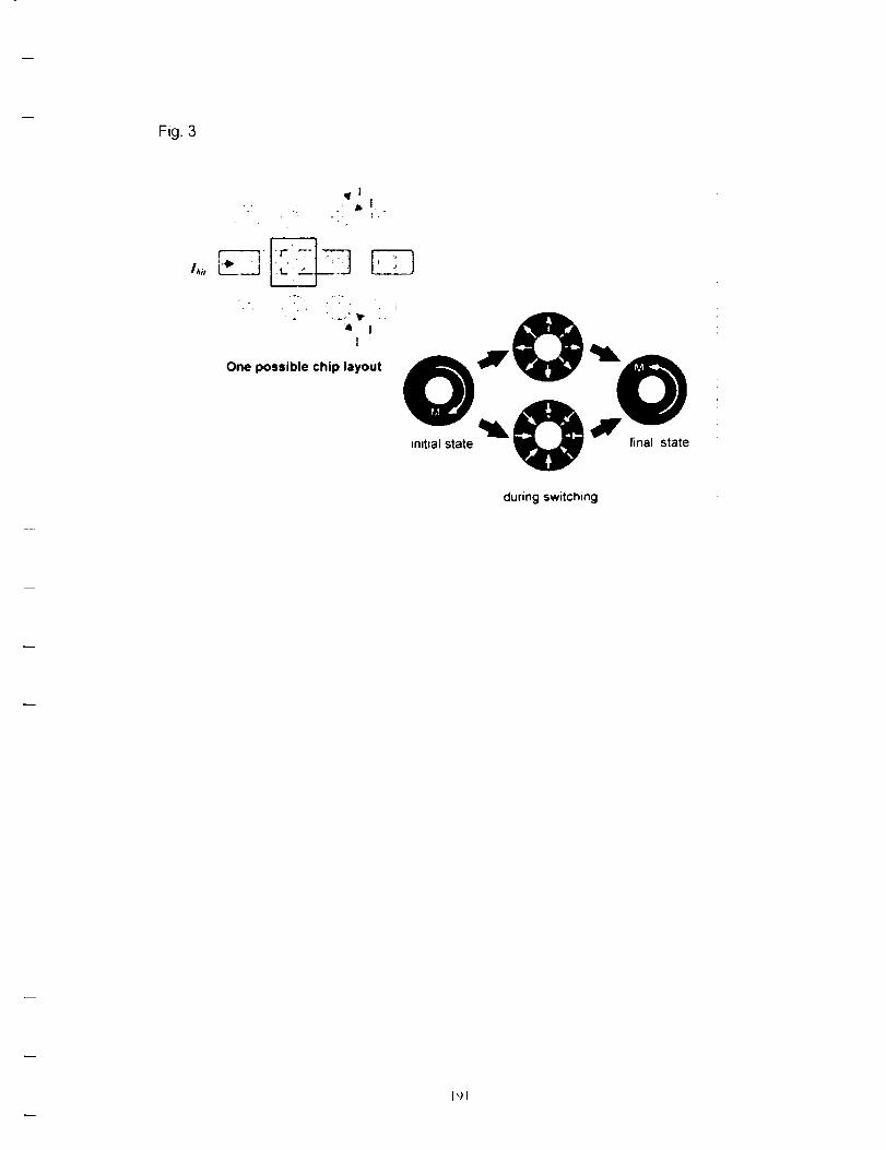
Fig. 3
,. _ • All l
I
One possible chip layout
during switching
1_]

Fig.4
State"0'
©
State "1'
©
R_. RLc;IRt'tCP.
Voltage.,
•._ V:0
2
W>O
Tm'_e
192

Fig. 5
(b)
193

/
Criteria for Magnetic Tunnel Junctions
Presenter: I Schuller, Universi_' of Calitbrnia-- San Diego
Material for this presentation was not available at the time of publication
194

Non Volatile Memory Technology Symposium 2001 NASA's Jet Propulsion Laboratory High-Performance Computing Center
A Modified MRAM Architecture
without a Current Rectifier Per Cell
Frank Wang
School of lnfonnatics and Multinmdia Technology.
[Jnivcrsib of North l,ondon.
166-220 Holloway Road, l,ondon N7 8DB. Lnited Kingdom
Tel +44 20 7607 7002. I:ax: -44 870 734 9255
E-mail f.wang'a!unl.acuk
Abstract-- lhis paper modifies the magnetic RAM
(MRAM) architecture by removing a current rectifier per
cell without sacrificing performance. A read operation of
stored data is maintained by introducing a simple concept
of "virtual ground" of operational amplifier. The modified
MRAM design offers a reduced element area with a little
penalty of an addition of one switch per column, which
occupies a very small silicon area. As a result, a tenfold
improvemem in storage density has been achieved by, an
experimental device
1ABIJ'. O1: CONTENI S
1 INTRODUCTION
2 ARCHIT[:,CTURAI, MODIFICATION
3 ENGINEERING REAI,1ZATION
4 CONCI.USIONS
I. INTRODUCTION
Unlike the semiconductor RAMs, magnetic random
access memory (MRAM) that stores information as the
orientation of magnetization of a thin ferromagnetic film
can hold stored information for long periods of time, and
is thus inherently nonvolatile. Nonvolatile memory can
be used as reliable caching to improve I/O performance
by reducing the I/O bottleneck between processor and
mechanical disk in a general computing system[l]
Nonvolatile memory also plays a significant role in
today's handheld device and mobile computing
environment, such as personal digital assistants (PDAs),
calculators, notebooks, and palmtops, etc[2]. MRAM with
the capability of being rewritten allows the end-user to
store their application and file data. Storage of system
configuration and control code in the form of an MRAM
allows the OEM to provide field updates to their software.
MRAM is a solid state memory which is light and does
not have the mechanical limitations of a disk drive.
MRAM also exhibits some excellent properties superior
to other solid state memories such as battery-backed
CMOS RAM and [lash memory The information stored
in CMOS RAM must not be critical to the product, as
battery failure is most certain to happen during the
lifetime of the product From the throughput point of
view, the slov_ erase and write times of flash memory,
result directly from the ffmdamentals of the flash memory
technology itself and any effort to accelerate the process
by, using higher voltages will shorten the life of thc
memory.
rd line
•
Bit line
High R -_
High R 4-=- i
t ;-I_.vR ---_f)
Junction --t ....
Diode _._
ZHighR e==_=_1
i
Figure 1 The traditional MRAM architecture with a diode perbit.
1'-t5
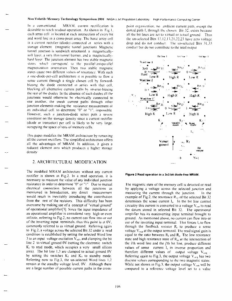
Non Volatile Memory Technology Symposium 2001 NASA's Jet Propulsion Laboratory
In a conventional MRAM. currenl rectification is
desirable to ,each readout operation. As shown m Fig. 1,each array cell is located at each intersection of every bitand word line in a cross-point array. The basic array cellis a current rectifier (diode) connected in series with a
storage element (magnetic tunnel junction). Magnetictunnel junction is sandwich structured: a magnetically-soft layel, a very thin tunnel barrier, and a magnetically-
hard layer The junction elemenl has two stable magneticslales which correspond to the parallel'antiparallelmagnetzzation orientation Then t,ao stable magneticstates cause two different values of resistance. With such
a one-diode-per-cell architecture it is possible to flow a
sense current through a single chosen cell by forward-biasing the diode connected in series with that cell,blocking all alternative currenl paths b) reverse-biasing
the rest of the diodes. In the absence of such diodes all the v_.,iunctions would otherwise be electrically connected toone another, the sneak current paths through other : "junction elements making the resistance measurement otan individual cell. to determine "0" or "1", impossiblettowever, such a junction-diode series puts a severeconstraint on the storage density since a current rectifier
(diode o_ transistor) per cell is likely to be very large.occupying the space of tens of memory cells.
Ihis papel modifies the MRAM architecture by removingall the current rectifiers The simplified architecture offersall the advantages of MRAM. In addition, it gives areduced element area which produces a higher storagedensity
2. ARCHITECTURAl, MODIFICATION
High Performance Computing Center
poinl organization, no ambient current path, except thedotted path I_ through the chosen Bit 32, exists because
all the bit lines are set to ,,irtual or actual ground. Thusthe tin-selected Bits 11,12,13.21,22,23 have zero voltagedrop and do not conduct. Thc un-selcctcd Bits 31,33
conduct bul do not contribute to the read output
9,11]ll_" I
0 _Hard
l.ow R
÷ -0 i_.Bll ?
Low R
w,,m i,i_ 7 b"_- Q- I
Bit ..1l
tltgh R b
K.#
lift filL" ' i_ll ]let' ]
H i," I,, . 1"_,It _
" _ 0 °
thgh R lx_w Ro i
@ @
BIl_-_ Bil ;,J
ihgh R High R
t " . + • *
t) , _, ii__
K: K_ "m,c_le ;
Viill_l :i t R [_Jolm d ,'i,:,
RK-- ,a_lput
,_.• 4- V,..!
The modified MRAM architecture without any currentrectifier is shown in Fig.2. In a read operation, it isnecessary to measure the value of any individual junctionresistance in order to determine "0" or "I". Due to mutual
electrical connection between all the junctions asmentioned in Introduction, any direct measurementwould result in inevitably introducing the contributionfrom the rest of the resistors• This difficulty has beenovercome by making use of a concept of "virtual ground"
of operational amplifier[3]. Since the input impedance ofan operational amplifier is considered very high or eveninfinite, referring to Fig.2, no current can flow into or out
of the inverting input terminals, thus this point is at 0V,commonly referred to as virtual ground. Referring againto Fig2, a voltage across the selected Bit 32 under a readcondition is established by setting the selected Word line
3 to an input voltage excitation V,.._, and damping the bitline 2 to virtual ground 0V (setting the electronic switch
K2 to read mode, which occupies a very small siliconarea). The bit line 1,3 are clamped to actual ground 0Vby setting the switches Ki and K_ to standby mode.Referring now to Fig3, the un-selected Word lines 1,2remain at the standby voltage level, 0V• Although thereare a large number of possible current paths in the cross-
Figure 2 Read operation in a 3x3 bit diode-free MRAM.
The magnetic state of the memory cell is detected or readby applying a voltage across the selected .junction andmeasuring the current through the junction. In theexample of Fig.2, the resistance R_2 of the selected Bit 32determines the sense current I_. In the bit line control
circuitry this current is converted to a voltage V,,,, to readthe datum stored in selected Bit 32. The operationalamplifier has its noninverting input terminal brought toground. As mentioned above, no current can flow into orout of the inverting input terminal• This forces I_ to flow
through the feedback resistor R_ to produce a sensevoltage Vou_jat the output terminal. The read signal gain isequal to the ratio between Rf and R,. The low resistancestate and high resistance state of R o, at the intersection ofthe i'th word line and the j'th bit line, produce differentvalues of sense current I_ in inverse proportion and
therefore different values of output voltage V,,, u .Referring again to Fig3, the output voltage V<,,u has twodiscrete values corresponding to the two ma,gmetic states.While not shown in Fig.3, the output voltage Vo_,¢_will becompared to a reference voltage level set to a value
196

Non Volatile Memory Technology Symposiunl ZOOI NASA's Jet Propulsion laboratory
half,,vay between the expected values for the lwo possiblestates of the mcrnor_, cell and thc diffcrenct, will bcamplified further to provide fldl logic levels After thedata is read, referring again to Fig;, the voltagc on Wordlinc 3 is returned to the standby value The magnetic
state remains unchanged aflev the read operation
_'rtte Rind + u,:., Write Read ! _ "
I - - I-,-Nmi+dl_--0 + _ 0 "" :'gmnd
High-Performance Computing Center
to directly access the junctions vdthout any' diode ortransistor current rectifier Thcoutput voltagcgives twodiscrete values (the vohagc difference is 06 mV)corresponding to the two magnetic states The proposedarchitecture is workable
•)id _r P'r
II 1"
,Id Ii,w 'ill v
,rd li_: ,:0 1,,
wd lle t
lin_ 2_v
hf_111,'
:ld write i',m'_'_ l.wy._ i
IJl,'111_ , i,.rarer_tIt_ i
;'¢ t:lllrell( I ¢ , ",;
_in"
( I!
",in
(llll
High R [ o',,,e R
Figure 3 Voltage and current levels during MRAM read and
write operations,
Figure 4 Micrographs of an MRAM without any currentrectifier.
In a write operation, sufficiently large currents, suppliedby a voltage source through load resistors, are passedthrough both a word line and a bit line, and the self-fieldof the combined currents at the intersection of the
energized word and bit lines will rotate the magnetizationof magnetically-soft layer of the single particularjunction located at the intersection• As illustrated in Fig.3,the (actual) ground of the energized lines ensures that allthe bits in contact with the energized word and bit lineshave zero voltage drop and do not conduct, otherwise theleakage currents may damage the junctions•
3. ENGINEERING REAI.IZATION
To realize this first architectural demonstration of diode-
free MRAM, reported to date, a multibit memory chipletwas fabricated, as shown in Fig.4. The junctiondimension is 2 im and the corresponding storage densityis 5 MegaBits/cm:. Contact windows were opened in theinsulator layer in order for the top leads and bottom leads
4. CONCLUSION
Storage density and access time are the twin keys tocomputer data storage devices. Although new electronicdevices, processor organizations and software havecontributed to enormous advances in computer
technology, they would have been worthless without thedenser and faster memories that were developed with
them. Magnetic RAM (MRAM) is a very importanttechnology for applications where the nonvolatility, fastaccess, higher density, in-system reprogrammability,radiation hardness and low power consumption are
required[4]. This paper modifies the traditional MRAMarchitecture by removing all the current rectifiers, whichare used to block the ambient current paths in a readoperation. The new architecture makes use of a simple
concept of "virtual ground" of operational amplifier[5].The modified MRAM design offers a reduced elementarea with a little penalty of an addition of one switch percolumn, which occupies a very small silicon area. The
197

Non Volatile Memory Technology Symposium Z001 NASA's Jet Propulsion Laboratory
overall improvement in storage density is over tenfold.
An engineering device with this new architecture has been
tested. No performance has been sacrificed and, in
addition, the fabrication process has been greatly
simplified.
REFERENCES
[1] M Baker, S. Asami, E. Deprit, J. Ousterhout, and M.
Seltzer, "Non-volatile memory for fast, reliable file
systems", Proceedings of the 5th International Conference
on Architectural Support for Programming Languages and
Operating System(ASPI,OS), Boston, pp.10-22, ACM
Press, 1992
[2] B. Bickford, "Nonvolatile memory requirements in a
mobile computing environment", International
NonVolatile Memory Technology Conference, 1996
[3] F. Hughes, Op Amp Handbook, Prentice Hall,
London, 1993
[4] S.Tehrani, B. Engel, JM.Slaughter, E.Chen,
M.DeHerrera, M.Durham, P.Naji, R. Whig, J. Janesky
and J. Calder, "'Recent development in magnetic tunnel
junction MRAM", IEEE Transaction, MAG-36, NoS,
pp.2752, September, 2000
[5]F. Wang, Diode-Free Cross-Point Array Architecture
for Magnetic Random Access Memories, GB and US
patent pending, 15 September, 1999
High-Performance Computing Center
and Technology for the 2 Ith Century Edited by Springer
To date, he has been invited to give 6 public lectures on
this invention by universities or institute in Japan, UK,
Portugal, Netherlands and Belgium. So fat, he has
published 50 Journal papers and 40 Conference
Proceeding papers. His research interest coxers Web
Database, llierarchical Storage Management (ttSM).
Nonvolatile RAM-based Mobile Database, RAID Mass
Storage, Network-Attached Storage, l--Commerce and
Multimedia, etc. He is nov, supervising 2 PhD students
and 8 MSc students and 8 undergraduate students.
Biography
Dr. Frank Wang is now a Senior Lecturer at School of
lnformatics and Multimedia Technology, University of
North London, United Kingdom. He obtained B.Sc. in
Computer Science, MSc. in Computer Science, Ph.D. in
Information Technology at University of Plymouth, UK.
In 1995, he invented a new concept Magnetic Random
Access Memory (MRAM) using spin-tunneling effects as
a new computer data storage device. This high-speed and
high-capacity digital memory is a combination of
traditional semiconductive memory and magnetic hard
disk but shares the advantages of the above two. This is
his most favourite contribution during his career, which
brought him to the attention of the international
community. Recently, he contributed two book chapters
concerning this invention in Encyclopedia of Science and
Technology edited by Elsevier and Frontiers of Science
198

l°
NVMTS2001 SURVEY
Please take a moment to complete this Survey and return at your convenience
What the one main reason you decided to attend NVMTS2001
2. Did we meet your need satisfactorily?
3. What one item do you feel needs the most improvement? How?
4. Your thoughts on the Symposium facility
. If you were to attend this Symposium next year, where would you like it to be
conducted? Last yearis was on the East Coast, would an East-West alternationbe beneficial? Would a Pacific Rim location be better? Or Americais mid-west?
6. Any other thoughts and comments you may have.
When completed, please mail to
Karl Strauss, 4800 Oak Grove Dr, MS 303-310, Pasadena, CA 91109
Thank you.