njg1157pcd gps and glonass front-end module · gps and glonass front-end module ... the njg1157pcd...
TRANSCRIPT
NJG1157PCD
- 1 - Ver.2016-04-18
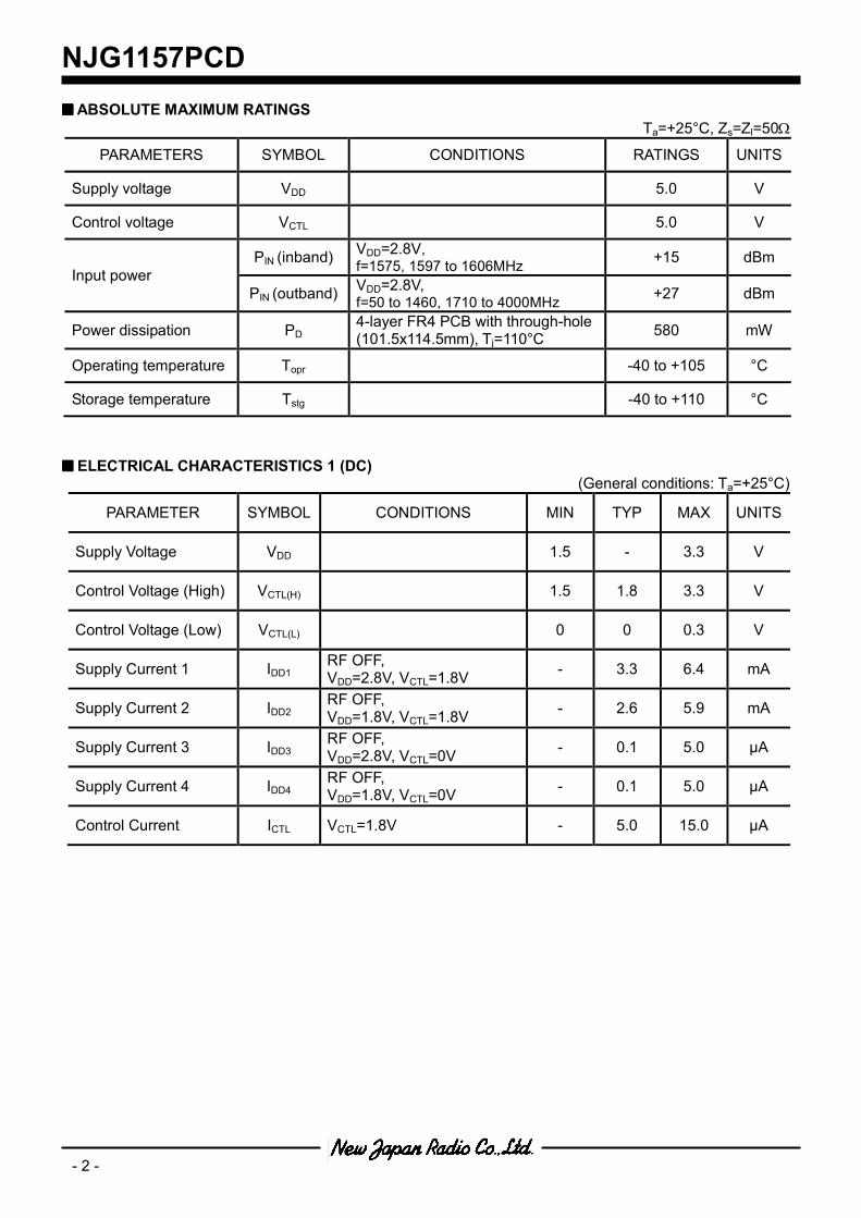
Pre-FilterRF OUTRF IN
VDDVCTL
LNA
Post-Filter
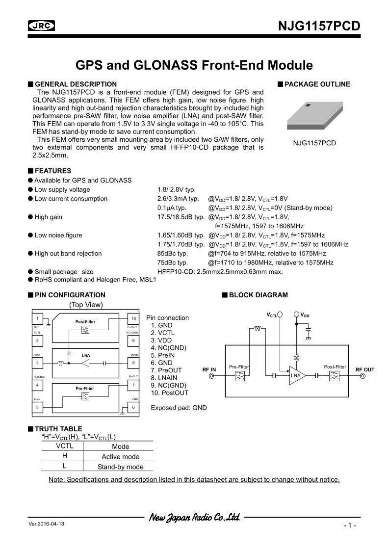
GPS and GLONASS Front-End Module GENERAL DESCRIPTION PACKAGE OUTLINE
The NJG1157PCD is a front-end module (FEM) designed for GPS and GLONASS applications. This FEM offers high gain, low noise figure, high linearity and high out-band rejection characteristics brought by included high performance pre-SAW filter, low noise amplifier (LNA) and post-SAW filter. This FEM can operate from 1.5V to 3.3V single voltage in -40 to 105°C. This FEM has stand-by mode to save current consumption.
This FEM offers very small mounting area by included two SAW filters, only two external components and very small HFFP10-CD package that is 2.5x2.5mm.
FEATURES
Available for GPS and GLONASS
Low supply voltage 1.8/ 2.8V typ.
Low current consumption 2.6/3.3mA typ. @VDD=1.8/ 2.8V, VCTL=1.8V
0.1µA typ. @VDD=1.8/ 2.8V, VCTL=0V (Stand-by mode)
High gain 17.5/18.5dB typ. @VDD=1.8/ 2.8V, VCTL=1.8V,
f=1575MHz, 1597 to 1606MHz
Low noise figure 1.65/1.60dB typ. @VDD=1.8/ 2.8V, VCTL=1.8V, f=1575MHz
1.75/1.70dB typ. @VDD=1.8/ 2.8V, VCTL=1.8V, f=1597 to 1606MHz
High out band rejection 85dBc typ. @f=704 to 915MHz, relative to 1575MHz
75dBc typ. @f=1710 to 1980MHz, relative to 1575MHz
Small package size HFFP10-CD: 2.5mmx2.5mmx0.63mm max.
RoHS compliant and Halogen Free, MSL1 PIN CONFIGURATION BLOCK DIAGRAM
TRUTH TABLE
“H”=VCTL(H), “L”=VCTL(L)
VCTL Mode
H Active mode
L Stand-by mode
Note: Specifications and description listed in this datasheet are subject to change without notice.
(Top View)
Pin connection 1. GND 2. VCTL 3. VDD 4. NC(GND) 5. PreIN 6. GND 7. PreOUT 8. LNAIN 9. NC(GND) 10. PostOUT Exposed pad: GND
NJG1157PCD
Pre-Filter
LNA
Post-Filter
GND
3
2
4
VCTL
5
1
8
9
7
6
10
VDD
NC(GND)
PreIN
PreOUT
GND
LNAIN
NC (GND)
PostOUT
- 2 -
NJG1157PCD
ABSOLUTE MAXIMUM RATINGS
Ta=+25°C, Zs=Zl=50Ω
PARAMETERS SYMBOL CONDITIONS RATINGS UNITS
Supply voltage VDD 5.0 V
Control voltage VCTL 5.0 V
Input power
PIN (inband) VDD=2.8V,
f=1575, 1597 to 1606MHz +15 dBm
PIN (outband) VDD=2.8V, f=50 to 1460, 1710 to 4000MHz
+27 dBm
Power dissipation PD 4-layer FR4 PCB with through-hole (101.5x114.5mm), Tj=110°C
580 mW
Operating temperature Topr -40 to +105 °C
Storage temperature Tstg -40 to +110 °C
ELECTRICAL CHARACTERISTICS 1 (DC)
(General conditions: Ta=+25°C)
PARAMETER SYMBOL CONDITIONS MIN TYP MAX UNITS
Supply Voltage VDD 1.5 - 3.3 V
Control Voltage (High) VCTL(H) 1.5 1.8 3.3 V
Control Voltage (Low) VCTL(L) 0 0 0.3 V
Supply Current 1 IDD1 RF OFF, VDD=2.8V, VCTL=1.8V
- 3.3 6.4 mA
Supply Current 2 IDD2 RF OFF, VDD=1.8V, VCTL=1.8V
- 2.6 5.9 mA
Supply Current 3 IDD3 RF OFF, VDD=2.8V, VCTL=0V
- 0.1 5.0 µA
Supply Current 4 IDD4 RF OFF, VDD=1.8V, VCTL=0V
- 0.1 5.0 µA
Control Current ICTL VCTL=1.8V - 5.0 15.0 µA
NJG1157PCD
- 3 -
ELECTRICAL CHARACTERISTICS 2 (RF)
General conditions: VDD=2.8V, VCTL=1.8V, fRF=1575MHz, 1597 to 1606MHz, Ta=+25°C, Zs=Zl=50Ω, with application circuit
PARAMETER SYMBOL CONDITIONS MIN TYP MAX UNITS
Small Signal Gain (GPS)1
GainGPS1 f=1575MHz (GPS), Exclude PCB, Connector Losses (0.19dB)
17.0 18.5 - dB
Small Signal Gain (GLONASS)1
GainGLN1 f=1597 to 1606MHz (GLONASS) Exclude PCB, Connector Losses (0.19dB)
17.0 18.5 - dB
Noise Figure (GPS)1
NFGPS1 f=1575MHz (GPS) Exclude PCB, Connector Losses (0.09dB)
- 1.6 2.1 dB
Noise Figure (GLONASS)1
NFGLN1 f=1597 to 1606MHz (GLONASS) Exclude PCB, Connector Losses (0.09dB)
- 1.7 2.2 dB
Input Power at 1dB Gain Compression Point 1
P-1dB(IN)1 f=1575, 1597 to 1606MHz - -15.0 - dBm
Input 3rd Order Intercept Point 1
IIP3_1 f1=1575MHz, f2=f1+/- 1MHz, Pin=-30dBm
- -3.0 - dBm
Out of Band Input 2nd Order
Intercept Point 1 IIP2_OB1
f1=824.6MHz at +15dBm, f2=2400MHz at +15dBm, fmeas=1575.4MHz
- +72 - dBm
Out of Band Input 3rd Order
Intercept Point 1 IIP3_OB1
f1=1712.7MHz at +15dBm, f2=1850MHz at +15dBm, fmeas=1575.4MHz
- +50 - dBm
700MHz Harmonic1 2fo1
Input jammer tone: 787.76MHz at +15dBm Measure the harmonic tone at 1575.52MHz
- -30 - dBm
Out-of-Band Input Power 1dB Compression 1
P-1dB(IN) _OB1-1
fjam=900MHz, fmeas=1575MHz at Pin=-40dBm
- +24 - dBm
P-1dB(IN) _OB1-2
fjam=1710MHz, fmeas=1575MHz at Pin=-40dBm
- +24 - dBm
Low Band Rejection 1 BR_L1 f=704 to 915MHz, relative to 1575MHz
- 85 - dBc
High Band Rejection 1 BR_H1 f=1710 to 1980MHz, relative to 1575MHz
- 75 - dBc
WLAN Band Rejection 1 BR_W1 f=2400 to 2500MHz, relative to 1575MHz
- 72 - dBc
RF IN Return Loss (GPS)1
RLiGPS1 f=1575MHz (GPS) - 7.5 - dB
RF IN Return Loss (GLONASS)1
RLiGLN1 f=1597 to 1606MHz (GLONASS) - 7.5 - dB
RF OUT Return Loss (GPS)1
RLoGPS1 f=1575MHz (GPS) - 11 - dB
RF OUT Return Loss (GLONASS)1
RLoGLN1 f=1597 to 1606MHz (GLONASS) - 15 - dB
Group Delay Time Deviation 1
GDTD1 f=1597 to 1606MHz (GLONASS) - 8.0 - ns
- 4 -
NJG1157PCD
ELECTRICAL CHARACTERISTICS 3 (RF)
General conditions: VDD=1.8V, VCTL=1.8V, fRF=1575MHz, 1597 to 1606MHz, Ta=+25°C, Zs=Zl=50Ω, with application circuit
PARAMETER SYMBOL CONDITIONS MIN TYP MAX UNITS
Small Signal Gain (GPS)2
GainGPS2 f=1575MHz (GPS) Exclude PCB, Connector Losses (0.19dB)
15.5 17.5 - dB
Small Signal Gain (GLONASS)2
GainGLN2 f=1597 to 1606MHz (GLONASS) Exclude PCB, Connector Losses (0.19dB)
15.5 17.5 - dB
Noise Figure (GPS)2
NFGPS2 f=1575MHz (GPS) Exclude PCB, Connector Losses (0.09dB)
- 1.65 2.20 dB
Noise Figure (GLONASS)2
NFGLN2 f=1597 to 1606MHz (GLONASS) Exclude PCB, Connector Losses (0.09dB)
- 1.75 2.35 dB
Input Power at 1dB Gain Compression Point 2
P-1dB(IN)2 f=1575, 1597 to 1606MHz - -17.0 - dBm
Input 3rd Order Intercept Point 2
IIP3_2 f1=1575MHz, f2=f1+/- 1MHz, Pin=-30dBm
- -6.0 - dBm
Out of Band Input 2nd Order
Intercept Point 2 IIP2_OB2
f1=824.6MHz at +15dBm, f2=2400MHz at +15dBm, fmeas=1575.4MHz
- +72 - dBm
Out of Band Input 3rd Order
Intercept Point 2 IIP3_OB2
f1=1712.7MHz at +15dBm, f2=1850MHz at +15dBm, fmeas=1575.4MHz
- +50 - dBm
700MHz Harmonic2 2fo2
Input jammer tone: 787.76MHz at +15dBm Measure the harmonic tone at 1575.52MHz
- -30 - dBm
Out-of-Band Input Power 1dB Compression 2
P-1dB(IN) _OB2-1
fjam=900MHz, fmeas=1575MHz at Pin=-40dBm
- +24 - dBm
P-1dB(IN) _OB2-2
fjam=1710MHz, fmeas=1575MHz at Pin=-40dBm
- +24 - dBm
Low Band Rejection 2 BR_L2 f=704 to 915MHz, relative to 1575MHz
- 85 - dBc
High Band Rejection 2 BR_H2 f=1710 to 1980MHz, relative to 1575MHz
- 75 - dBc
WLAN Band Rejection 2 BR_W2 f=2400 to 2500MHz, relative to 1575MHz
- 72 - dBc
RF IN Return Loss (GPS)2
RLiGPS2 f=1575MHz (GPS) - 7.5 - dB
RF IN Return Loss (GLONASS)2
RLiGLN2 f=1597 to 1606MHz (GLONASS) - 7.5 - dB
RF OUT Return Loss (GPS)2
RLoGPS2 f=1575MHz (GPS) - 10 - dB
RF OUT Return Loss (GLONASS)2
RLoGLN2 f=1597 to 1606MHz (GLONASS) - 13 - dB
Group Delay Time Deviation 2
GDTD2 f=1597 to 1606MHz (GLONASS) - 8.0 - ns
NJG1157PCD
- 5 -
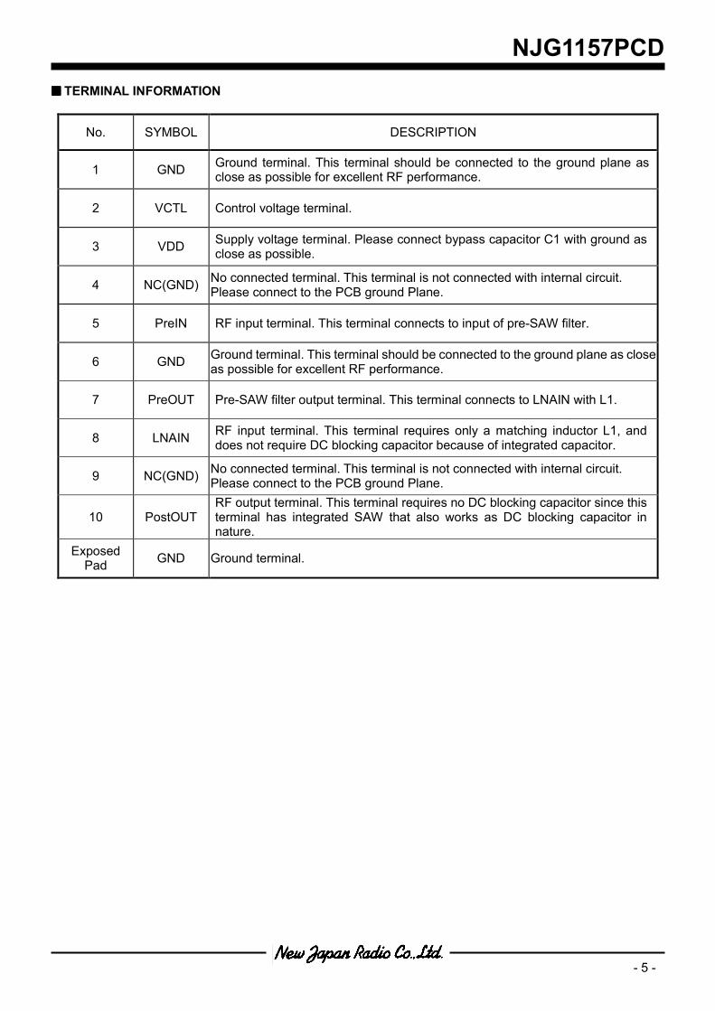
TERMINAL INFORMATION
No. SYMBOL DESCRIPTION
1 GND Ground terminal. This terminal should be connected to the ground plane as close as possible for excellent RF performance.
2 VCTL Control voltage terminal.
3 VDD Supply voltage terminal. Please connect bypass capacitor C1 with ground as close as possible.
4 NC(GND) No connected terminal. This terminal is not connected with internal circuit. Please connect to the PCB ground Plane.
5 PreIN RF input terminal. This terminal connects to input of pre-SAW filter.
6 GND Ground terminal. This terminal should be connected to the ground plane as close as possible for excellent RF performance.
7 PreOUT Pre-SAW filter output terminal. This terminal connects to LNAIN with L1.
8 LNAIN RF input terminal. This terminal requires only a matching inductor L1, and does not require DC blocking capacitor because of integrated capacitor.
9 NC(GND) No connected terminal. This terminal is not connected with internal circuit. Please connect to the PCB ground Plane.
10 PostOUT RF output terminal. This terminal requires no DC blocking capacitor since this terminal has integrated SAW that also works as DC blocking capacitor in nature.
Exposed Pad
GND Ground terminal.

- 6 -
NJG1157PCD
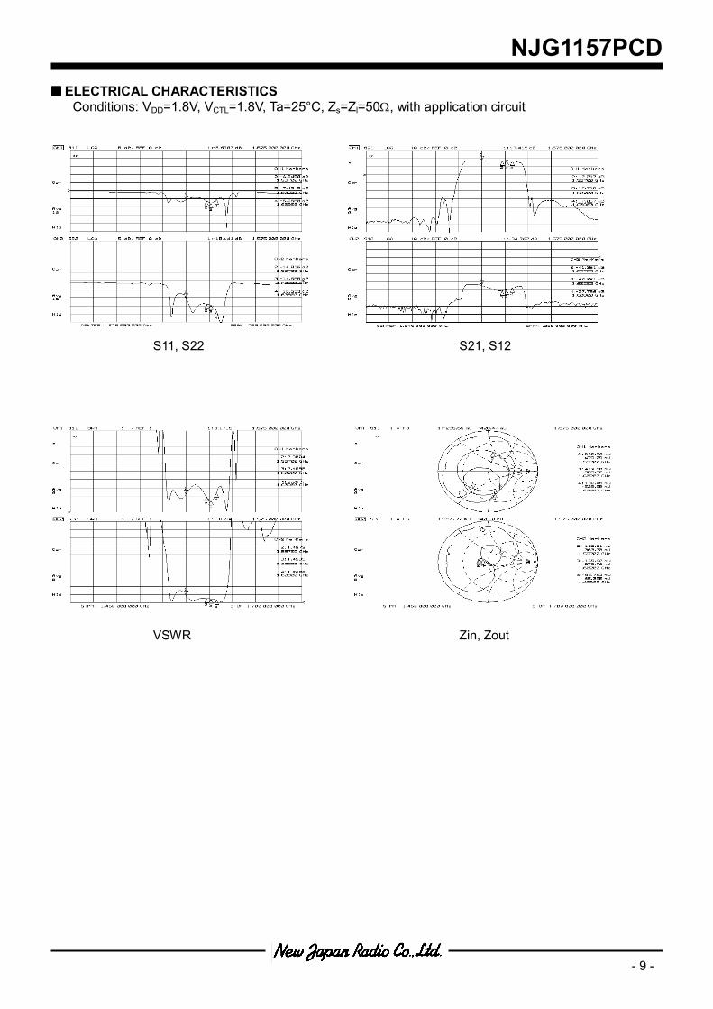
ELECTRICAL CHARACTERISTICS
Conditions: VDD=2.8V, VCTL=1.8V, Ta=25°C, Zs=Zl=50Ω, with application circuit
S11, S22 S21, S12
VSWR Zin, Zout

NJG1157PCD
- 7 -
0
1
2
3
4
0
5
10
15
20
1.54 1.56 1.58 1.60 1.62 1.64
NF, Gain vs. frequency(VDD=2.8V, VCTL=1.8V)
Noise Figure (dB)
Gain (dB)
frequency (GHz)
Gain
NF
(NF, Gain: Exclude PCB, Connector Losses)
-25
-20
-15
-10
-5
0
5
10
2
3
4
5
6
7
8
9
-40 -30 -20 -10 0 10
Pout, IDD vs. Pin(VDD=2.8V, VCTL=1.8V, fRF=1575MHz)
Pout (dBm)
IDD (mA)
Pin (dBm)
IDD
P-1dB(IN)=-14.1dBm
P-1dB(OUT)=+3.4dBm
Pout
-100
-80
-60
-40
-20
0
20
-40 -30 -20 -10 0 10
Pout, IM3 vs. Pin(VDD=2.8V, VCTL=1.8V, f1=1575MHz, f2=1576MHz)
Pout , IM3 (dBm)
Pin (dBm)
Pout
IM3
IIP3=-2.1dBm
OIP3=+15.7dBm
-80
-70
-60
-50
-40
-30
-20
-10
0
10
20
0.5 1.0 1.5 2.0 2.5 3.0
S21 (dB)
Frequency (GHz)
S21 vs. Frequency
(VDD=2.8V, V
CTL=1.8V)
ELECTRICAL CHARACTERISTICS
Conditions: VDD=2.8V, VCTL=1.8V, Ta=25°C, Zs=Zl=50Ω, with application circuit
0
10
20
30
40
50
1.54 1.56 1.58 1.60 1.62 1.64
Group Delay vs. frequency(VDD=2.8V, VCTL=1.8V)
Group Delay (ns)
frequency (GHz)

- 8 -
NJG1157PCD
-100
-80
-60
-40
-20
0
20
40
60
80
100
-40 -20 0 20 40 60 80
Out-of-band IIP2(V
DD=2.8V, V
CTL=1.8V, f
meas=1575.4MHz,
f1=824.6MHz, f2=2400MHz)
Pout , IM2 (dBm)
Pin (dBm)
Pout
IM2
IIP2_OB=+73.2dBm
6
8
10
12
14
16
18
20
22
-40 -30 -20 -10 0 10 20 30
Out-of-band P-1dB (fjam=1710MHz)(VDD=2.8V, VCTL=1.8V, f
meas=1575MHz at Pin=-40dBm)
Gain (dB)
Pin at 1710MHz (dBm)
Gain
P-1dB(IN)_OB > +24.0dBm
(Gain: Exclude PCB, Connector Losses)
6
8
10
12
14
16
18
20
22
-40 -30 -20 -10 0 10 20 30
Out-of-band P-1dB (fjam=900MHz)(VDD=2.8V, VCTL=1.8V, f
meas=1575MHz at Pin=-40dBm)
Gain (dB)
Pin at 900MHz (dBm)
Gain
P-1dB(IN)_OB > +24.0dBm(Gain: Exclude PCB, Connector Losses)
-120
-100
-80
-60
-40
-20
0
-30 -20 -10 0 10 20 30
2nd Harmonics(V
DD=2.8V, V
CTL=1.8V,
fin=787.76MHz, fmeas
=1575.52MHz)
2nd Harm
onics(dBm)
Pin(dBm)
2fo=-30.7dBm
-100
-80
-60
-40
-20
0
20
40
60
80
-40 -20 0 20 40 60
Out-of-band IIP3(VDD=2.8V, VCTL=1.8V, fmeas=1575.4MHz,
f1=1712.7MHz, f2=1850MHz)
Pout , IM3 (dBm)
Pin (dBm)
Pout
IM3
IIP3_OB=+57.8dBm
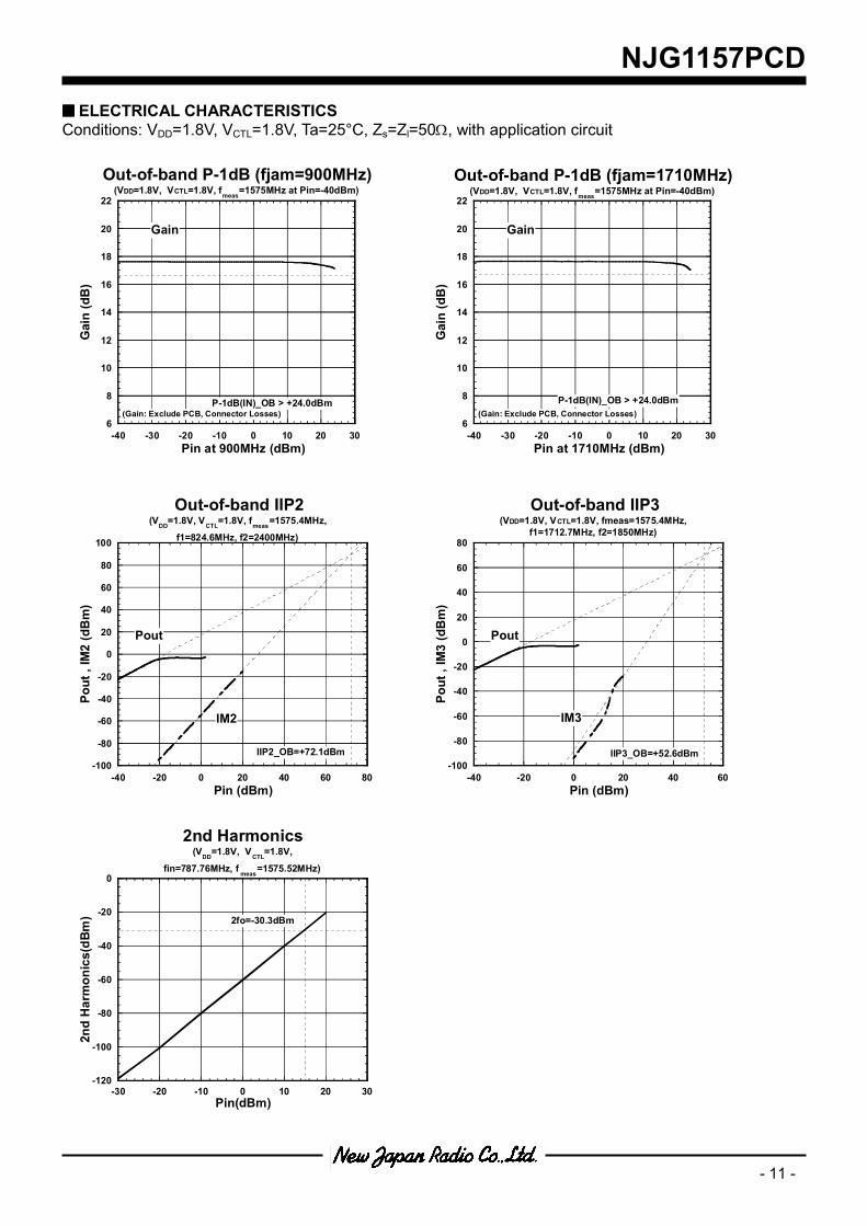
ELECTRICAL CHARACTERISTICS
Conditions: VDD=2.8V, VCTL=1.8V, Ta=25°C, Zs=Zl=50Ω, with application circuit
NJG1157PCD
- 9 -
ELECTRICAL CHARACTERISTICS
Conditions: VDD=1.8V, VCTL=1.8V, Ta=25°C, Zs=Zl=50Ω, with application circuit
S11, S22 S21, S12
VSWR Zin, Zout

- 10 -
NJG1157PCD
-100
-80
-60
-40
-20
0
20
-40 -30 -20 -10 0 10
Pout, IM3 vs. Pin(VDD=1.8V, VCTL=1.8V, f1=1575MHz, f2=1576MHz)
Pout , IM3 (dBm)
Pin (dBm)
Pout
IM3
IIP3=-5.8dBm
OIP3=+11.5dBm
-25
-20
-15
-10
-5
0
5
10
2
3
4
5
6
7
8
9
-40 -30 -20 -10 0 10
Pout, IDD vs. Pin(VDD=1.8V, VCTL=1.8V, fRF=1575MHz)
Pout (dBm)
IDD (mA)
Pin (dBm)
IDD
P-1dB(IN)=-17.0dBm
P-1dB(OUT)=-0.7dBm
Pout
0
10
20
30
40
50
1.54 1.56 1.58 1.60 1.62 1.64
Group Delay vs. frequency(VDD=1.8V, VCTL=1.8V)
Group Delay (ns)
frequency (GHz)
0
1
2
3
4
0
5
10
15
20
1.54 1.56 1.58 1.60 1.62 1.64
NF, Gain vs. frequency(VDD=1.8V, VCTL=1.8V)
Noise Figure (dB)
Gain (dB)
frequency (GHz)
Gain
NF
(NF, Gain: Exclude PCB, Connector Losses)-80
-70
-60
-50
-40
-30
-20
-10
0
10
20
0.5 1.0 1.5 2.0 2.5 3.0
S21 (dB)
Frequency (GHz)
S21 vs. Frequency
(VDD=1.8V, V
CTL=1.8V)
ELECTRICAL CHARACTERISTICS
Conditions: VDD=1.8V, VCTL=1.8V, Ta=25°C, Zs=Zl=50Ω, with application circuit
NJG1157PCD
- 11 -
-100
-80
-60
-40
-20
0
20
40
60
80
100
-40 -20 0 20 40 60 80
Out-of-band IIP2(V
DD=1.8V, V
CTL=1.8V, f
meas=1575.4MHz,
f1=824.6MHz, f2=2400MHz)
Pout , IM2 (dBm)
Pin (dBm)
Pout
IM2
IIP2_OB=+72.1dBm
6
8
10
12
14
16
18
20
22
-40 -30 -20 -10 0 10 20 30
Out-of-band P-1dB (fjam=1710MHz)(VDD=1.8V, VCTL=1.8V, f
meas=1575MHz at Pin=-40dBm)
Gain (dB)
Pin at 1710MHz (dBm)
Gain
P-1dB(IN)_OB > +24.0dBm
(Gain: Exclude PCB, Connector Losses)
6
8
10
12
14
16
18
20
22
-40 -30 -20 -10 0 10 20 30
Out-of-band P-1dB (fjam=900MHz)(VDD=1.8V, VCTL=1.8V, f
meas=1575MHz at Pin=-40dBm)
Gain (dB)
Pin at 900MHz (dBm)
Gain
P-1dB(IN)_OB > +24.0dBm(Gain: Exclude PCB, Connector Losses)
-120
-100
-80
-60
-40
-20
0
-30 -20 -10 0 10 20 30
2nd Harmonics(V
DD=1.8V, V
CTL=1.8V,
fin=787.76MHz, fmeas
=1575.52MHz)
2nd Harm
onics(dBm)
Pin(dBm)
2fo=-30.3dBm
-100
-80
-60
-40
-20
0
20
40
60
80
-40 -20 0 20 40 60
Out-of-band IIP3(VDD=1.8V, VCTL=1.8V, fmeas=1575.4MHz,
f1=1712.7MHz, f2=1850MHz)
Pout , IM3 (dBm)
Pin (dBm)
Pout
IM3
IIP3_OB=+52.6dBm
ELECTRICAL CHARACTERISTICS
Conditions: VDD=1.8V, VCTL=1.8V, Ta=25°C, Zs=Zl=50Ω, with application circuit
- 12 -
NJG1157PCD
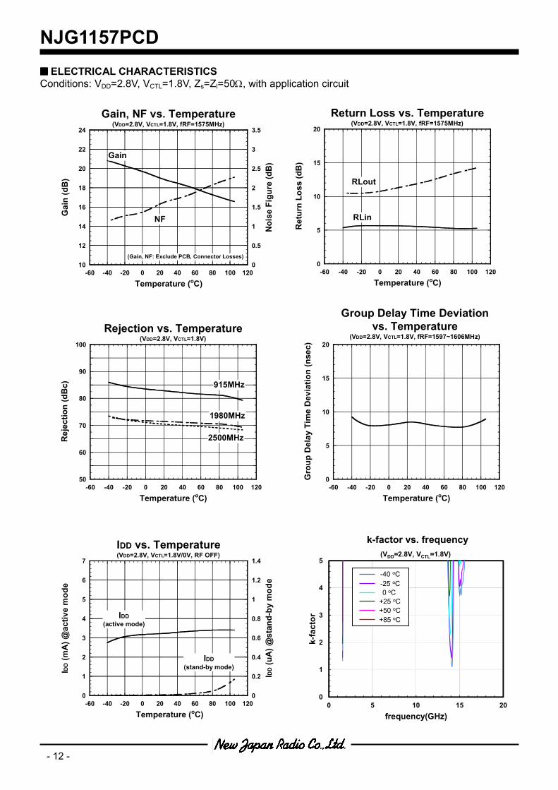
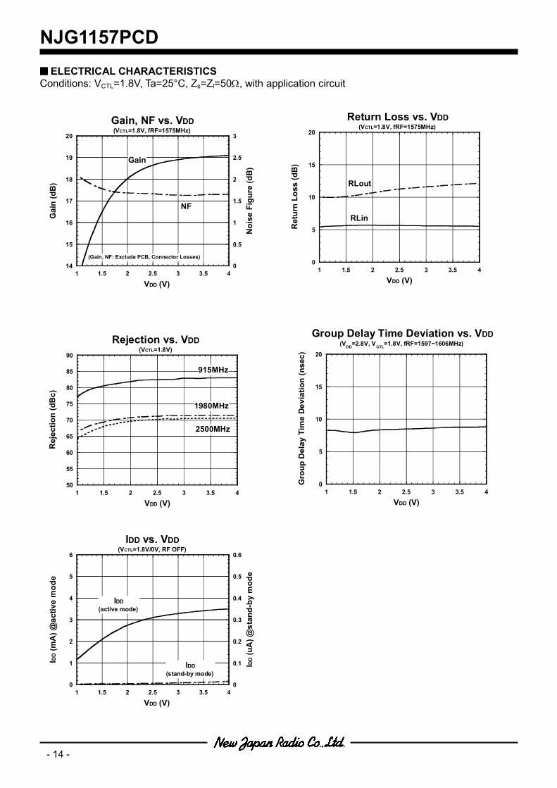
ELECTRICAL CHARACTERISTICS
Conditions: VDD=2.8V, VCTL=1.8V, Zs=Zl=50Ω, with application circuit
0
5
10
15
20
-60 -40 -20 0 20 40 60 80 100 120
Return Loss (dB)
Temperature (oC)
RLin
Return Loss vs. Temperature(VDD=2.8V, VCTL=1.8V, fRF=1575MHz)
RLout
50
60
70
80
90
100
-60 -40 -20 0 20 40 60 80 100 120
Rejection (dBc)
Temperature (oC)
1980MHz
Rejection vs. Temperature(VDD=2.8V, VCTL=1.8V)
915MHz
2500MHz
0
5
10
15
20
-60 -40 -20 0 20 40 60 80 100 120
Group Delay Tim
e Deviation (nsec)
Temperature (oC)
Group Delay Time Deviation
vs. Temperature(VDD=2.8V, VCTL=1.8V, fRF=1597~1606MHz)
0
1
2
3
4
5
6
7
0
0.2
0.4
0.6
0.8
1
1.2
1.4
-60 -40 -20 0 20 40 60 80 100 120
IDD (mA) @active m
ode
IDD (uA) @stand-by m
ode
Temperature (oC)
IDD(stand-by mode)
IDD vs. Temperature(VDD=2.8V, VCTL=1.8V/0V, RF OFF)
IDD(active mode)
10
12
14
16
18
20
22
24
0
0.5
1
1.5
2
2.5
3
3.5
-60 -40 -20 0 20 40 60 80 100 120
Gain (dB)
Noise Figure (dB)
Temperature (oC)
NF
Gain, NF vs. Temperature(VDD=2.8V, VCTL=1.8V, fRF=1575MHz)
Gain
(Gain, NF: Exclude PCB, Connector Losses)
0
1
2
3
4
5
0 5 10 15 20
k-factor
frequency(GHz)
k-factor vs. frequency
(VDD=2.8V, VCTL=1.8V)
-40 oC
-25 oC
0 oC
+25 oC
+50 oC
+85 oC
NJG1157PCD
- 13 -
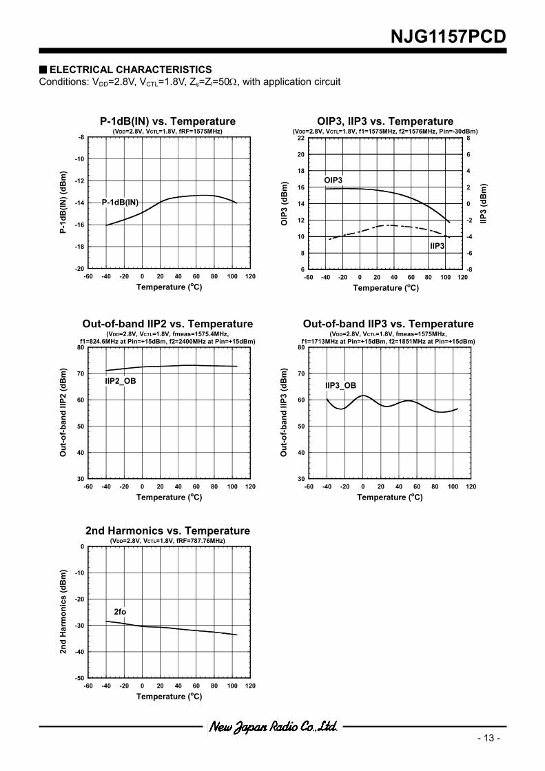
ELECTRICAL CHARACTERISTICS
Conditions: VDD=2.8V, VCTL=1.8V, Zs=Zl=50Ω, with application circuit
-20
-18
-16
-14
-12
-10
-8
-60 -40 -20 0 20 40 60 80 100 120
P-1dB(IN) (dBm)
Temperature (oC)
P-1dB(IN)
P-1dB(IN) vs. Temperature(VDD=2.8V, VCTL=1.8V, fRF=1575MHz)
6
8
10
12
14
16
18
20
22
-8
-6
-4
-2
0
2
4
6
8
-60 -40 -20 0 20 40 60 80 100 120OIP3 (dBm)
IIP3 (dBm)
Temperature (oC)
IIP3
OIP3, IIP3 vs. Temperature(VDD=2.8V, VCTL=1.8V, f1=1575MHz, f2=1576MHz, Pin=-30dBm)
OIP3
30
40
50
60
70
80
-60 -40 -20 0 20 40 60 80 100 120
Out-of-band IIP2 (dBm)
Temperature (oC)
IIP2_OB
Out-of-band IIP2 vs. Temperature(VDD=2.8V, VCTL=1.8V, fmeas=1575.4MHz,
f1=824.6MHz at Pin=+15dBm, f2=2400MHz at Pin=+15dBm)
30
40
50
60
70
80
-60 -40 -20 0 20 40 60 80 100 120
Out-of-band IIP3 (dBm)
Temperature (oC)
IIP3_OB
Out-of-band IIP3 vs. Temperature(VDD=2.8V, VCTL=1.8V, fmeas=1575MHz,
f1=1713MHz at Pin=+15dBm, f2=1851MHz at Pin=+15dBm)
-50
-40
-30
-20
-10
0
-60 -40 -20 0 20 40 60 80 100 120
2nd Harm
onics (dBm)
Temperature (oC)
2fo
2nd Harmonics vs. Temperature(VDD=2.8V, VCTL=1.8V, fRF=787.76MHz)
- 14 -
NJG1157PCD
0
5
10
15
20
1 1.5 2 2.5 3 3.5 4
Group Delay Tim
e Deviation (nsec)
VDD (V)
Group Delay Time Deviation vs. VDD(V
DD=2.8V, V
CTL=1.8V, fRF=1597~1606MHz)
0
5
10
15
20
1 1.5 2 2.5 3 3.5 4
Return Loss (dB)
VDD (V)
RLin
Return Loss vs. VDD(VCTL=1.8V, fRF=1575MHz)
RLout
14
15
16
17
18
19
20
0
0.5
1
1.5
2
2.5
3
1 1.5 2 2.5 3 3.5 4
Gain (dB)
Noise Figure (dB)
VDD (V)
NF
Gain, NF vs. VDD(VCTL=1.8V, fRF=1575MHz)
Gain
(Gain, NF: Exclude PCB, Connector Losses)
0
1
2
3
4
5
6
0
0.1
0.2
0.3
0.4
0.5
0.6
1 1.5 2 2.5 3 3.5 4
IDD (mA) @active m
ode
IDD (uA) @stand-by m
ode
VDD (V)
IDD(stand-by mode)
IDD vs. VDD(VCTL=1.8V/0V, RF OFF)
IDD(active mode)
50
55
60
65
70
75
80
85
90
1 1.5 2 2.5 3 3.5 4
Rejection (dBc)
VDD (V)
Rejection vs. VDD(VCTL=1.8V)
1980MHz
915MHz
2500MHz
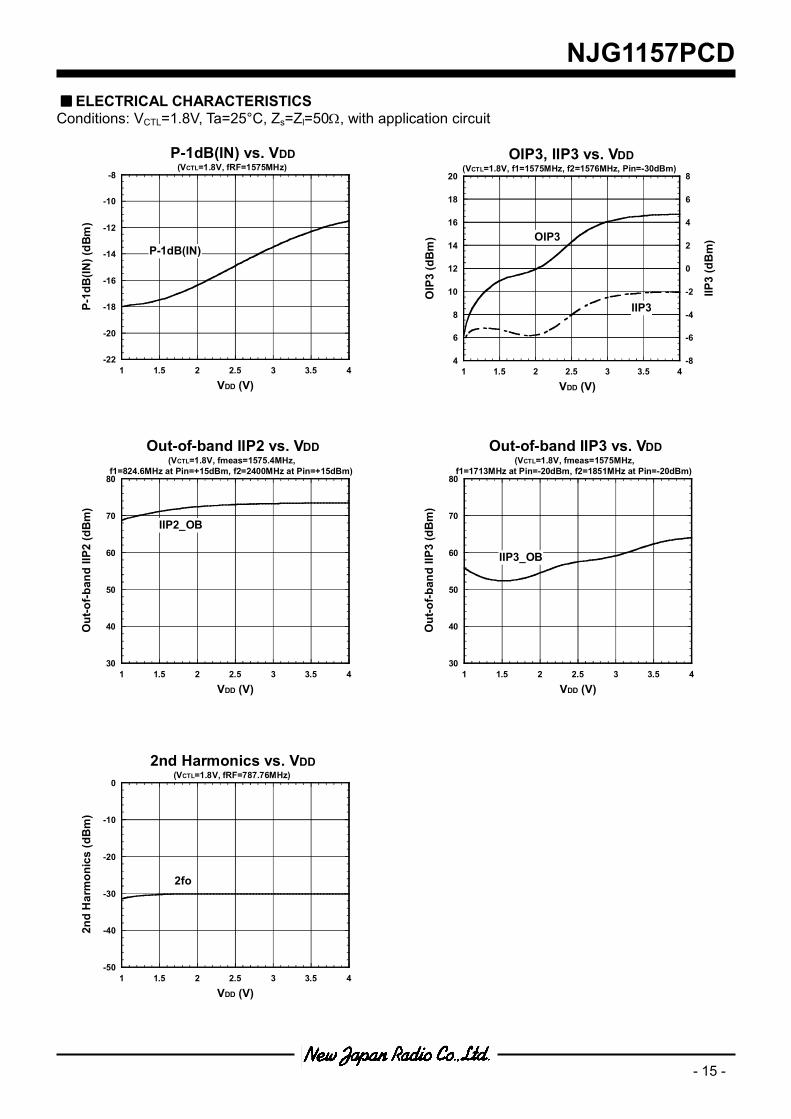
ELECTRICAL CHARACTERISTICS
Conditions: VCTL=1.8V, Ta=25°C, Zs=Zl=50Ω, with application circuit
NJG1157PCD
- 15 -
30
40
50
60
70
80
1 1.5 2 2.5 3 3.5 4
Out-of-band IIP3 (dBm)
VDD (V)
IIP3_OB
Out-of-band IIP3 vs. VDD(VCTL=1.8V, fmeas=1575MHz,
f1=1713MHz at Pin=-20dBm, f2=1851MHz at Pin=-20dBm)
30
40
50
60
70
80
1 1.5 2 2.5 3 3.5 4
Out-of-band IIP2 (dBm)
VDD (V)
IIP2_OB
Out-of-band IIP2 vs. VDD(VCTL=1.8V, fmeas=1575.4MHz,
f1=824.6MHz at Pin=+15dBm, f2=2400MHz at Pin=+15dBm)
4
6
8
10
12
14
16
18
20
-8
-6
-4
-2
0
2
4
6
8
1 1.5 2 2.5 3 3.5 4
OIP3 (dBm)
IIP3 (dBm)
VDD (V)
IIP3
OIP3, IIP3 vs. VDD(VCTL=1.8V, f1=1575MHz, f2=1576MHz, Pin=-30dBm)
OIP3
-22
-20
-18
-16
-14
-12
-10
-8
1 1.5 2 2.5 3 3.5 4
P-1dB(IN) (dBm)
VDD (V)
P-1dB(IN)
P-1dB(IN) vs. VDD(VCTL=1.8V, fRF=1575MHz)
-50
-40
-30
-20
-10
0
1 1.5 2 2.5 3 3.5 4
2nd Harm
onics (dBm)
VDD (V)
2fo
2nd Harmonics vs. VDD(VCTL=1.8V, fRF=787.76MHz)
ELECTRICAL CHARACTERISTICS
Conditions: VCTL=1.8V, Ta=25°C, Zs=Zl=50Ω, with application circuit
- 16 -
NJG1157PCD
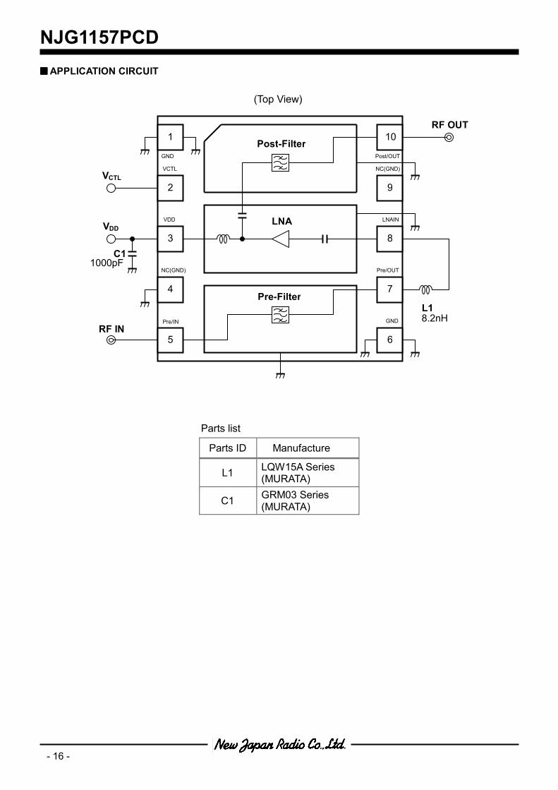
APPLICATION CIRCUIT
Parts ID Manufacture
L1 LQW15A Series (MURATA)
C1 GRM03 Series (MURATA)
Parts list
(Top View)
8.2nH
1000pF
RF OUT
RF IN
V DD
V CTL
L1
C1
GND
3
2
4
VCTL
5
1
8
9
7
6
10
VDD
NC(GND)
Pre/IN
Pre/OUT
GND
LNAIN
NC(GND)
Post/OUT
Pre-Filter
LNA
Post-Filter

NJG1157PCD
- 17 -
Evaluation board
<PCB LAYOUT GUIDELINE>
PRECAUTIONS • Please layout ground pattern under this FEM in order not to couple with RFIN and RFOUT terminal. • All external parts should be placed as close as possible to the FEM. • For good RF performance, all GND terminals must be connected to PCB ground plane of substrate, and via-holes for GND should be placed near the FEM.
PCB Substrate: FR-4 Thickness: 0.2mm
Microstrip line width: 0.4mm (Z0=50Ω) Size: 14.0mm x 14.0mm
RF IN
(Top View)
RF OUT
L1
C1
VCTL VDD
GND Via Hole
Diameter φ= 0.2mm, 0.4mm
PKG Terminal
PCB
PKG Outline
- 18 -
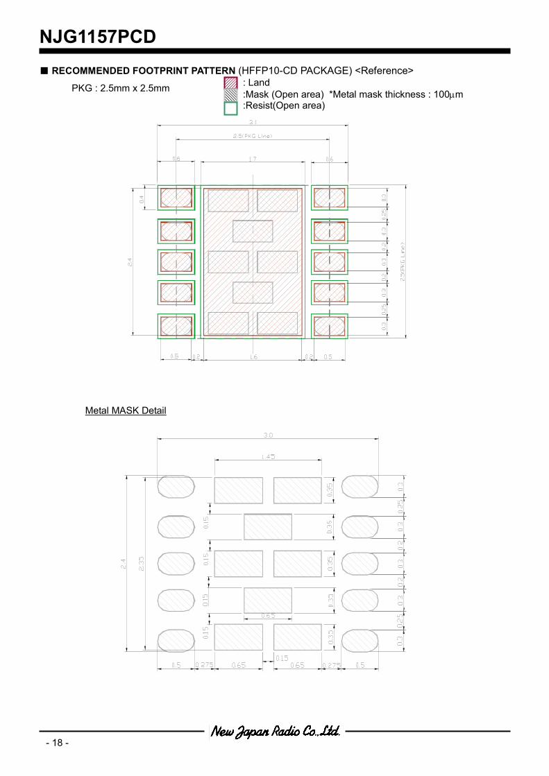
NJG1157PCD
RECOMMENDED FOOTPRINT PATTERN (HFFP10-CD PACKAGE) <Reference>
: Land
:Mask (Open area) *Metal mask thickness : 100µm :Resist(Open area)
Metal MASK Detail
PKG : 2.5mm x 2.5mm
NJG1157PCD
- 19 -
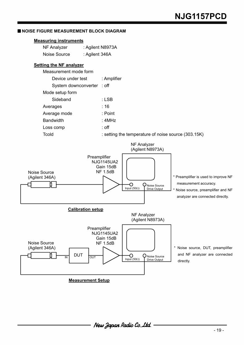
NOISE FIGURE MEASUREMENT BLOCK DIAGRAM
Calibration setup
Noise Source (Agilent 346A)
NF Analyzer (Agilent N8973A)
Input (50Ω) Noise Source Drive Output
* Preamplifier is used to improve NF
measurement accuracy.
* Noise source, preamplifier and NF
analyzer are connected directly.
Preamplifier NJG1145UA2
Gain 15dB NF 1.5dB
Measurement Setup
Noise Source (Agilent 346A)
DUT
NF Analyzer (Agilent N8973A)
Input (50Ω) Noise Source Drive Output
IN OUT
* Noise source, DUT, preamplifier
and NF analyzer are connected
directly.
Preamplifier NJG1145UA2
Gain 15dB NF 1.5dB
Measuring instruments
NF Analyzer : Agilent N8973A
Noise Source : Agilent 346A
Setting the NF analyzer
Measurement mode form
Device under test : Amplifier
System downconverter : off
Mode setup form
Sideband : LSB
Averages : 16
Average mode : Point
Bandwidth : 4MHz
Loss comp : off
Tcold : setting the temperature of noise source (303.15K)
- 20 -
NJG1157PCD
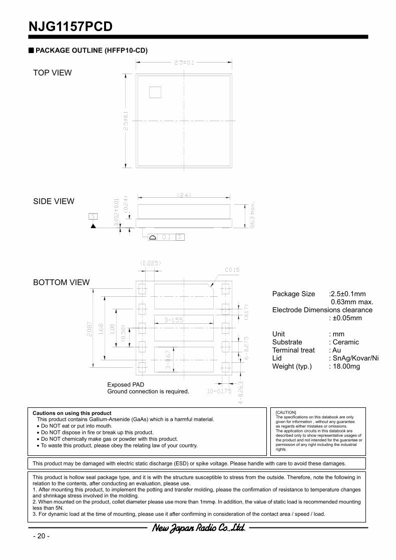
PACKAGE OUTLINE (HFFP10-CD)
Cautions on using this product This product contains Gallium-Arsenide (GaAs) which is a harmful material.
• Do NOT eat or put into mouth.
• Do NOT dispose in fire or break up this product.
• Do NOT chemically make gas or powder with this product.
• To waste this product, please obey the relating law of your country.
This product may be damaged with electric static discharge (ESD) or spike voltage. Please handle with care to avoid these damages.
[CAUTION] The specifications on this databook are only given for information , without any guarantee as regards either mistakes or omissions. The application circuits in this databook are described only to show representative usages of the product and not intended for the guarantee or permission of any right including the industrial
rights.
This product is hollow seal package type, and it is with the structure susceptible to stress from the outside. Therefore, note the following in relation to the contents, after conducting an evaluation, please use. 1. After mounting this product, to implement the potting and transfer molding, please the confirmation of resistance to temperature changes and shrinkage stress involved in the molding. 2. When mounted on the product, collet diameter please use more than 1mmφ. In addition, the value of static load is recommended mounting less than 5N. 3. For dynamic load at the time of mounting, please use it after confirming in consideration of the contact area / speed / load.
Package Size :2.5±0.1mm 0.63mm max.
Electrode Dimensions clearance : ±0.05mm
Unit : mm Substrate : Ceramic Terminal treat : Au Lid : SnAg/Kovar/Ni Weight (typ.) : 18.00mg
TOP VIEW
SIDE VIEW
BOTTOM VIEW
Exposed PAD Ground connection is required.