ni pxie-6555/6556 specificationsni pxie-6555/6556 specifications 200 mhz digital waveform...
TRANSCRIPT

NI PXIe-6555/6556 Specifications200 MHz Digital Waveform Generator/Analyzer with PPMU
This document provides the specifications for the NI PXIe-6555 (NI 6555) and the NI PXIe-6556 (NI 6556). Specifications are subject to change without notice. For the most recent NI 6555/6556 specifications, visit ni.com/manuals. To access the NI 6555/6556 documentation, including the NI Digital Waveform Generator/Analyzer Getting Started Guide, which contains functional descriptions of the NI 6555/6556 signals and the connector pinouts, navigate to Start»Programs»National Instruments»NI-HSDIO»Documentation.
Caution The NI 6555/6556 has a maximum operating temperature range of 0 ºC to +45 ºC in all NI PXI Express and hybrid NI PXI Express chassis.
Hot Surface If the NI 6555/6556 has been in use, it might exceed safe handling temperatures and cause burns. Allow time to cool before removing the NI 6555/6556 from the chassis.
Caution Refer to the Read Me First: Safety and Electromagnetic Compatibility document for important safety and electromagnetic compatibility information. To obtain a copy of this document online, visit ni.com/manuals, and search for the document title.
Caution To ensure the specified EMC performance, operate this product only with shielded cables and accessories.
Caution To ensure specified EMC performance, you must install PXI EMC Filler Panels, National Instruments part number 778700-01, in all open chassis slots.
Caution To ensure the specified EMC performance, all I/O cables must be no longer than 3 m (10 ft).
Note All values were obtained using a 1 m cable (SHC68-C68-D4 recommended). Performance specifications are not guaranteed when using longer cables.

2 | ni.com | NI PXIe-6555/6556 Specifications
TerminologyMaximum and minimum specifications are warranted not to exceed these values within certain operating conditions and include the effects of temperature and uncertainty unless otherwise noted.
Typical specifications are unwarranted values that are representative of a majority (3 σ) of units within certain operating conditions and include the effects of temperature and uncertainty unless otherwise noted.
Characteristic specifications are unwarranted values that are representative of an average unit operating at room temperature.
Nominal specifications are unwarranted values that are relevant to the use of the product and convey the expected performance of the product.
All specifications are Typical unless otherwise noted. These specifications are valid within the operating temperature range. Accuracy specifications are valid within ±5 ºC of self-calibration unless otherwise noted.
ContentsTerminology..............................................................................................................................2Channel Specifications .............................................................................................................3
Digital Generation Channels (DIO <0..23>, PFI 1, PFI 2, PFI 4, and PFI 5)...................4Digital Acquisition Channels (DIO <0..23>, PFI 1, PFI 2, PFI 4, and PFI 5)..................5Active Load Channels (Data <0..23> and PFI <1,2,4,5> Channels) ................................6PPMU Channels (DIO <0..23>, PFI 1, PFI 2, PFI 4, and PFI 5)......................................7General PFI Channels (PFI 0, PFI 3, and PFI <24..31>)..................................................14EXTERNAL FORCE and EXTERNAL SENSE Channels .............................................14CAL Channels................................................................................................................... 15
Timing Specifications ...............................................................................................................15Sample Clock....................................................................................................................15Generation Timing (Data, DDC CLK OUT, and PFI <0..3> Channels) ..........................18Generation Provided Setup and Hold Times ....................................................................20Acquisition Timing (Data, STROBE, and PFI <0..3> Channels).....................................22Setup and Hold Times to STROBE ..................................................................................24CLK IN (SMA Jack Connector) .......................................................................................27PFI 5 as STROBE (DDC Connector) ...............................................................................28PXIe_DStarA (PXI Express Backplane) ..........................................................................28CLK OUT (SMA Jack Connector) ...................................................................................29PFI 4 as DDC CLK OUT (DDC Connector) ....................................................................29Reference Clock (PLL) .....................................................................................................30
Waveform Specifications..........................................................................................................31Memory and Scripting ......................................................................................................31Triggers (Inputs to the NI 6556) .......................................................................................34Events (Generated from the NI 6556)...............................................................................35Miscellaneous ...................................................................................................................36
NI PXIe-6555/6556 Specifications | © National Instruments | 3
Power ................................................................................................................................ 36Physical............................................................................................................................. 37I/O Panel Connectors........................................................................................................ 37Software............................................................................................................................ 38Environment ..................................................................................................................... 38Safety ................................................................................................................................ 39Electromagnetic Compatibility......................................................................................... 39CE Compliance................................................................................................................. 40Online Product Certification............................................................................................. 40Environmental Management............................................................................................. 40
Where to Go for Support .......................................................................................................... 41
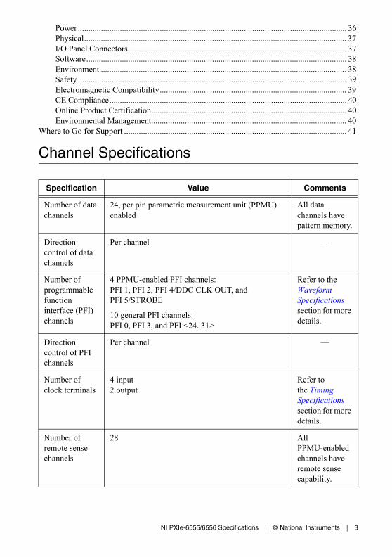
Channel Specifications
Specification Value Comments
Number of data channels
24, per pin parametric measurement unit (PPMU) enabled
All data channels have pattern memory.
Direction control of data channels
Per channel —
Number of programmable function interface (PFI) channels
4 PPMU-enabled PFI channels:PFI 1, PFI 2, PFI 4/DDC CLK OUT, and PFI 5/STROBE
10 general PFI channels:PFI 0, PFI 3, and PFI <24..31>
Refer to the Waveform Specifications section for more details.
Direction control of PFI channels
Per channel —
Number of clock terminals
4 input2 output
Refer to the Timing Specifications section for more details.
Number of remote sense channels
28 All PPMU-enabled channels have remote sense capability.

4 | ni.com | NI PXIe-6555/6556 Specifications
Digital Generation Channels (DIO <0..23>, PFI 1, PFI 2, PFI 4, and PFI 5)
Note These features are controlled independently per channel.
Specification Value Comments
Generation signal type
Single-ended, ground referenced. —
Programmable generation voltage levels
Drive Voltage High Level (VOH)
Drive Voltage Low Level (VOL)
Drive Tristate (VTT)
—
Generation voltage range
-2 V to 6 V (default) or -1 V to 7 V Software-selectable.
Generation voltage resolution
122 μV —
DC generation voltage accuracy
±5 °C of Self-Calibration
±15 °C of Self-Calibration
Maximum accuracy when operating within the specified self-calibration temperature range.
±11 mV ±16 mV
Generation voltage swing
400 mV to 8.0 V Into a 1 MΩ load. Power limitations may restrict the number of channels toggling at full voltage swing.
Output impedance
50 Ω Nominal.

NI PXIe-6555/6556 Specifications | © National Instruments | 5
Digital Acquisition Channels (DIO <0..23>, PFI 1, PFI 2, PFI 4, and PFI 5)
Note These features are controlled independently per channel.
Maximum allowed DC drive strength per channel
±35 mA Nominal. Do not exceed the maximum power limit of the device.
Data channel tristate control
Per channel, per cycle Software-selectable and hardware-timed.
Channel power-on state
Drivers disabled, high impedance —
Output protection
The device can indefinitely sustain a short to any voltage between -3 V and 8.5 V provided that you observe the maximum drive strength limitations.
—
Specification Value Comments
Acquisition signal type
Single-ended, ground referenced —
Programmable acquisition voltages
Compare Voltage High Threshold (VIH)
Compare Voltage Low Threshold (VIL)
Termination Voltage (VTT)
—
Acquisition voltage threshold range
-2 V to 7 V —
Acquisition and termination voltage resolution
122 μV —
Termination voltage range
-2 V to 6 V (default) or -1 V to 7 V —
Specification Value Comments

6 | ni.com | NI PXIe-6555/6556 Specifications
Active Load Channels (Data <0..23> and PFI <1,2,4,5> Channels)
Note Active Loads are supported only for the NI 6556.
Note These features are controlled independently per channel.
DC acquisition voltage accuracy
±5 °C of Self-Calibration
±15 °C of Self-Calibration
Maximum accuracy when operating within the specified self-calibration temperature range between -1.5 V and 6.8 V.
(VIL) = ±25 mV
(VIH) = ±25 mV
(VTT) = ±11 mV
(VIL) = ±28 mV
(VIH) = ±28 mV
(VTT) = ±16 mV
Minimum detectable voltage swing
50 mV —
Input impedance High-impedance or 50 Ω terminated into VTT. Software-selectable.
High impedance leakage
<5 nA Characteristic.
Input protection The device can indefinitely sustain a short to any voltage between -3 V and 8.5 V, provided that you observe the maximum drive strength limitations.
—
Specification Value Comments
Programmable levels
Commutating Voltage (VTT)
Current Source (ISOURCE)
Current Sink (ISINK)
—
Load
Range Resolution
Accuracy (±15 °C of
Self-Calibration)
Typical accuracy with 3 V overdrive.
1.5 mA to 24 mA
488 nA ±1 mA
Specification Value Comments

NI PXIe-6555/6556 Specifications | © National Instruments | 7
PPMU Channels (DIO <0..23>, PFI 1, PFI 2, PFI 4, and PFI 5)
Note These features are controlled independently per channel.
Figure 1. Characteristic Quadrant Behavior by Current Range
Specification Value Comments
PPMU signal type
Single-ended, ground referenced Referenced to the ground pins on the VHDCI connector.
Programmable levels
Force voltage (FV)
Force current (FI)
Voltage clamp high (VCHI)
Voltage clamp low (VCLO)
Voltage clamps are only active when forcing current.
110
100
80
60
40
20
0
–20
–40
–60
–80
–100
–110–2.5 –2 –1 0 1 2 3 4 5 6 7 7.5
Per
cent
of C
urre
nt R
ange
(%
)
Voltage (V)
Guaranteed
8 mA and 32 mA Ranges
128 μA, 512 μA, and 2 mA Ranges
2 μA, 8 μA, and 32 μA Ranges

8 | ni.com | NI PXIe-6555/6556 Specifications
Specification Value Comments
Force voltage
Ranges Resolution
Accuracy within ±5 °C
of Self-Calibration
Accuracy within
±15 °C of Self-
Calibration
Maximum accuracy at the sense location.
-2 V to 6 V (default)
-1 V to 7 V
122 μV ±11 mV ±16 mV
Force voltage settling time
Current Range Settling Time Settled to 1% of the final value. 1 V steps with 50% of the current range load into 100 pF.
2 μA 150 μs
8 μA 75 μs
32 μA, 128 μA, 512 μA 40 μs
2 mA 45 μs
8 mA 55 μs
32 mA 60 μs
Load capacitance
Current Range Capacitance These values represent the allowed load capacitance through a 1 m SHC68-C68-D4 cable to ensure a well-behaved transient response.
2 μA 1 nF
8 μA 1 nF
32 μA 1 nF
128 μA 1 nF
512 μA 4.7 nF
2 mA 10 nF
8 mA 47 nF
32 mA 100 nF

NI PXIe-6555/6556 Specifications | © National Instruments | 9
Characteristic Step Response
Figure 2. Characteristic Step Response into a Capacitive Load in the 2 μA Range
Figure 3. Characteristic Step Response into a Capacitive Load in the 512 μA Range
1.75
0.00
0
Time (μs)
Am
plitu
de (
V)
1.50
1.25
1.00
0.75
0.50
0.25
100 150 250 350 45050 200 300 400 500
1 nF470 pF100 pF
0
Time (μs)
Am
plitu
de (
V)
25 50 75 100 125
1.75
0.00
1.50
1.25
1.00
0.75
0.50
0.25
4.7 nF1 nF
470 pF
10 | ni.com | NI PXIe-6555/6556 Specifications
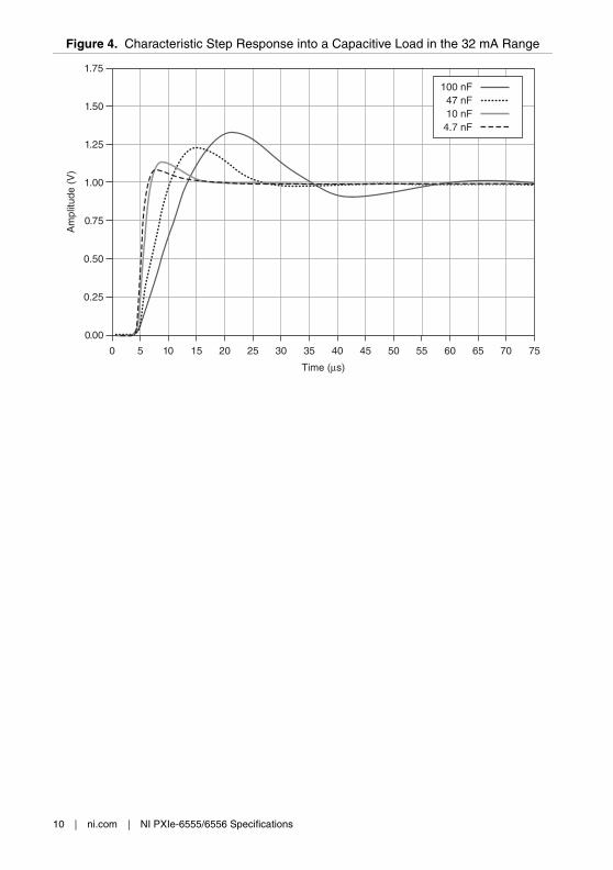
Figure 4. Characteristic Step Response into a Capacitive Load in the 32 mA Range
0
Time (μs)
Am
plitu
de (
V)
155 10 20 25 30 35 40 50 55 65 7045 60 75
1.75
0.00
1.50
1.25
1.00
0.75
0.50
0.25
100 nF47 nF10 nF4.7 nF

NI PXIe-6555/6556 Specifications | © National Instruments | 11
Specification Value Comments
Force current resolution
Current Range Resolution Nominal.
±2 μA 60 pA
±8 μA 240 pA
±32 μA 980 pA
±128 μA 3.9 nA
±512 μA 15.6 nA
±2 mA 60 nA
±8 mA 240 nA
±32 mA 980 nA
Force current accuracy
Accuracy within ±5 °C of
Self-Calibration
Accuracy within ±15 °C of
Self-Calibration
Maximum.
1% of range 1.3% of range
Force current voltage clamps
Current Range Resolution
Accuracy within ±15 °C
of Self-Calibration
Maximum. Voltage clamps begin to conduct within 700 mV of the programmable voltage level.
VCLO -2 V to 6 V
122 μV ±100 mV
VCHI -1 V to 7 V
Note: (VCHI - VCLO) > 1 V
Aperture time range
4 μs to 65 ms —
Aperture time resolution
4 μs —
Measure voltage
Range Resolution
Accuracy within ±15 °C
of Self-Calibration
Maximum accuracy at the sense location with one 60 Hz PLC aperture.
-2 V to 7 V 228 μV ±3 mV

12 | ni.com | NI PXIe-6555/6556 Specifications
Figure 5. Typical Voltage Measurement Noise for Given Aperture Times
Specification Value Comments
Measure current resolution
Current Range Resolution Nominal.
±2 μA 460 pA
±8 μA 1.8 nA
±32 μA 7.3 nA
±128 μA 30 nA
±512 μA 120 nA
±2 mA 460 nA
±8 mA 1.8 μA
±32 mA 7.3 μA
Measure current accuracy
Accuracy within ±5 °C of
Self-Calibration
Accuracy within ±15 °C of
Self-Calibration
Maximum accuracy with one 60 Hz PLC aperture.1% of range 1.3% of range
500
0
1 μ
Aperture Time (s)
RM
S N
oise
(μV
)
450
400
300
350
250
200
150
100
50
10 μ 100 μ 1 m 10 m 100 m
Remote SenseLocal Sense

NI PXIe-6555/6556 Specifications | © National Instruments | 13
Figure 6. Typical Current Measurement Noise for Given Aperture Times
Note IRMS Noise is represented by the following equation:
IRMS Noise = (RMS Noise × Current Range) / 106
For example, 100 ppm on a 32 mA range yields a noise of 3.2 μA RMS.
3.2 μA RMS = (100 ppm × 32 mA) / 106
Specification Value Comments
I/O switch resistance
5.5 Ω Nominal.
Remote feedback impedance
100 kΩ Nominal.
Output protection
The device can indefinitely sustain a short to any voltage between -3 V and 8.5 V, provided that you observe the maximum drive strength limitations.
—
600
0
1 μ
Aperture Time (s)
RM
S N
oise
(pp
m o
f Cur
rent
Ran
ge)
550
500
450
350
400
300
250
100
150
200
50
10 μ 100 μ 1 m 10 m 100 m
32 mA Range512 μA Range32 μA Range
2 μA Range

14 | ni.com | NI PXIe-6555/6556 Specifications
General PFI Channels (PFI 0, PFI 3, and PFI <24..31>)
EXTERNAL FORCE and EXTERNAL SENSE Channels
Note These specifications are valid for the EXTERNAL FORCE and EXTERNAL SENSE channels on the AUX I/O connector or on the REMOTE SENSE connector. The AUX I/O connector is available only on NI 6556 devices.
Specification Value Comments
Circuit type PFI 0 and PFI 3: High-speed I/O circuits
PFI <24..31>: 5 V compatible I/O circuits
—
Generation voltage level
Low Voltage Levels, Characteristic
High Voltage Levels, Characteristic
Nominal.
0 V 3.3 V
Drive strength
PFI 0 and PFI 3: ±33 mA
PFI <24..31>: ±85 mA
—
Output impedance
50 Ω Nominal.
Output protection
The device can indefinitely sustain a short to any voltage between 0 V and 5 V.
—
Acquisition voltage level
Low Voltage Thresholds
High Voltage Thresholds
Nominal.
0.8 V 2 V
Input protection PFI 0 and PFI 3: -1 V to 5 V
PFI <24..31>: -1 V to 6.5 V
Maximum.
Specification Value Comments
Direction EXTERNAL FORCE: input to the device
EXTERNAL SENSE: output from the device
—
Analog bandwidth
EXTERNAL FORCE: 3 MHz
EXTERNAL SENSE: 30 kHz
Characteristic with a single channel connected.
Range -2 V to 7 V —

NI PXIe-6555/6556 Specifications | © National Instruments | 15
CAL Channels
Note These specifications are valid for the CAL channel on the AUX I/O connector and on the REMOTE SENSE connector. The AUX I/O connector is available only on NI 6556 devices.
Timing Specifications
Sample Clock
Maximum current
±32 mA Valid for EXTERNAL FORCE only.
Input protection The device can indefinitely sustain a short to any voltage between -3 V and 8.5 V, provided that you observe the maximum drive strength limitations.
—
Specification Value Comments
Direction Output from the NI 6556 during external calibration. This channel is in a high-impedance or undriven state during normal operation.
—
Voltage level 5 V Nominal.
Drive strength 1 mA Maximum allowed. Sourcing only.
Specification Value Comments
Sample clock sources
1. Onboard Clock
2. CLK IN (SMA jack connector)
3. PXIe_DStarA (PXI Express backplane)
4. STROBE (Digital Data & Control (DDC)connector; acquisition only)
—
On Board Clock frequency range
800 Hz to 200 MHz —
Specification Value Comments

16 | ni.com | NI PXIe-6555/6556 Specifications
On Board Clock frequency resolution
<0.1 Hz NI-HSDIO may be queried for the programmed frequency value.
On Board Clock frequency accuracy
±150 ppm Nominal. Accuracy may be increased by using a higher performance external Reference clock.
CLK IN frequency range
20 kHz to 200 MHz Refer to the CLK IN (SMA Jack Connector) section for restrictions based on waveform type.
PXIe_DStarA frequency range
800 Hz to 200 MHz Refer to the PXIe_DStarA (PXI Express Backplane) section for more information.
STROBE frequency range
800 Hz to 200 MHz Refer to the PFI 5 as STROBE (DDC Connector) section for more information.
Sample clock relative delay adjustment range
±5 ns To align multiple devices, apply a delay or phase adjustment to the On Board Clock.Sample clock
relative delay adjustment resolution
3.125 ps
Exported Sample clock destinations
1. DDC CLK OUT (DDC connector)
2. CLK OUT (SMA jack connector)
Internal Sample clocks with sources other than STROBE can be exported.
Specification Value Comments

NI PXIe-6555/6556 Specifications | © National Instruments | 17
Figure 7. Characteristic Period Jitter (RMS) versus Frequency
Exported Sample clock offset range (tCO)
0 ns to 2.4 ns Software programmable.
Exported Sample clock offset resolution (tCO)
13 ps
Exported Sample clock offset accuracy (tCO)
±200 ps Software programmable.
Exported Sample clock duty cycle (DDC CLKOUT)
Minimum Maximum 3.3 V at maximum clock rate (200 MHz).
Not including the effects of system crosstalk.
42% 55%
Exported Sample clock period jitter
24 psrms Characteristic; using On Board Clock.
Specification Value Comments
30
25
20
15
Per
iod
Jitte
r (p
s R
MS
)
On Board Clock Frequency (MHz)
10
5
0100 120 140 160 180 200
0 °C
25 °C
45 °C

18 | ni.com | NI PXIe-6555/6556 Specifications
Generation Timing (Data, DDC CLK OUT, and PFI <0..3> Channels)
Figure 8 shows an eye diagram of a 200 Mbps pseudorandom bit sequence (PRBS) waveform at 3.3 V. This waveform was captured on a characteristic DIO channel at room temperature into high-impedance.
Figure 8. Characteristic Eye Diagram at 3.3 V
Specification Value Comments
Maximum data rate per channel
200 Mbps
Supported for all logic families
—
Maximum data channel toggle rate
3.3 V swing: 100 MHz
5 V swing: 50 MHz
Toggle rates exceeding these values may invalidate CE certifications. Refer to the Electromagnetic Compatibility section for more information.
Vol
tage
(V
)
3.50
–0.50
3.00
2.50
2.00
1.50
1.00
0.50
0.00

NI PXIe-6555/6556 Specifications | © National Instruments | 19
Figure 9 shows an eye diagram of a 200 Mbps PRBS waveform at 0.4 V. This waveform was captured on a characteristic DIO channel at room temperature into high-impedance.
Figure 9. Characteristic Eye Diagram at 0.4 V
Specification Value Comments
Data channel-to-channel skew
NI 6555 NI 6556 There will be additional skew from crosstalk, acquisition threshold, and other transmission line effects in your system. You may see up to 150 ps of additional skew from differences between channels in the average rate of pattern transitions.
Maximum: 750 ps Characteristic: 300 ps
Maximum: 600 ps Characteristic: 300 ps
Data position modes
Sample clock rising edge
Sample clock falling edge
Delay from Sample clock rising edge
—
Generation data delay frequency
On Board Clock External Clock —
All supported frequencies
Frequencies ≥ 20 MHz
Vol
tage
(V
)
0.50
–0.10
0.40
0.30
0.20
0.10
0.00

20 | ni.com | NI PXIe-6555/6556 Specifications
Generation Provided Setup and Hold Times
Generation data delay range
-1 to 2 Sample clock cycles, expressed as a fraction of the Sample clock period
The sum of data delay and data deskew may not exceed -2 to 3 Sample clock cycles.Generation data
deskew range-2 to 3 Sample clock cycles, expressed as a time in seconds
Generation data delay and data deskew resolution
30 ps Nominal.
Specification
Value
NI 6555/6556
Provided Setup Time (tPSU) tp - tCO - 850 psCharacteristic
Provided Hold Time (tPH) tCO - 700 ps
Exported Sample Clock Offset (tCO) is software programmable.
Compare the setup and hold times from the datasheet of your device under test (DUT) to the values in the table above. The provided setup and hold times must be greater than the setup and hold times required for the DUT. If you require more setup time, configure your exported Sample clock mode to Inverted and/or delay your clock or data relative to the Sample clock.
Refer to Figure 10 for a diagram illustrating the relationship between the exported Sample clock mode and the provided setup and hold times.
Notes: This table assumes the data position is set to Sample clock rising edge and the noninverted Sample clock is exported to the DDC connector with tCO programmed using exported Sample clock offset.
Specification Value Comments

NI PXIe-6555/6556 Specifications | © National Instruments | 21
Figure 10. Generation Provided Setup and Hold Times Timing Diagram
Note Provided setup and hold times account for maximum channel-to-channel skew and jitter.
tP = = Period of Sample Clock
tPH = Provided Hold Time
tPSU = Provided Setup Time
tPCO = Time from Rising Clock Edge to Data Transition (Provided Clock to Out Time)
tCO = Exported Sample Clock Offset
tPSU
tPCO
tP
ExportedSample Clock
DATA CHANNELS
Data PositionRising Edge
(Noninverted Clock,tCO = 1.25 ns)
Data PositionRising Edge
(Inverted Clock,tCO = 0 ns)
tPH
tPH tPSU
tPCO
1ƒ

22 | ni.com | NI PXIe-6555/6556 Specifications
Figure 11. Generation Timing Diagram
Exported Sample Clockwith non-zero tCO
Exported Sample ClockInverted
Exported Sample ClockNoninverted
DATA CHANNELSData Position Rising Edge
Data Position Delayed (δG)
Sample Clock
Sample n Sample n+1
Sample n Sample n+1
Sample n Sample n+1
tSCDDCtP
tCO
δG
Sample n Sample n+1
δD
Sample n
Data Position Delayedand Deskewed (δD)
tSCDDC : Time Delay from Sample Clock (Internal) to DDC Connector
–1 ≤ δG ≤ 2 : Pattern Generation Channel Data Delay (Fraction of tP)
δD = Pattern Generation Channel Deskew (Time)
tCO = Exported Sample Clock Offset
tP = = Period of Sample Clock1ƒ
Data Position Falling Edge

NI PXIe-6555/6556 Specifications | © National Instruments | 23
Acquisition Timing (Data, STROBE, and PFI <0..3> Channels)
Figure 12. Typical Overdrive Dispersion Adjustment
Note Timing calibration executes with 1.25 V of overdrive.
Specification Value Comments
Maximum data rate per channel
200 Mbps —
Channel-to-channel skew
NI 6555 NI 6556 There will be additional skew from crosstalk, acquisition threshold, overdrive, dispersion, and transmission line effects. You may see up to 175 ps of additional skew from differences between channels in the average rate of pattern transitions.
Maximum: 725 ps Characteristic: 300 ps
Maximum: 600 ps Characteristic: 300 ps
Overdrive Voltage (V)
Del
ay (
s)
0.0
–250 p
–500 p
0 p
500 p
750 p
250 p
1 n
0.2 0.4 0.6 0.8 1.0 1.2 1.4 1.81.6 2.0 2.2 2.4 2.6 2.8 3.0

24 | ni.com | NI PXIe-6555/6556 Specifications
Setup and Hold Times to STROBE
Specification Value Comments
Data position modes Sample clock rising edge
Sample clock falling edge
Delay from Sample clock rising edge
—
Acquisition data delay and deskew frequency
Onboard Clock External Clock —
All supported frequencies Frequencies ≥ 20 MHz
Acquisition data delay range
-1 to 2 Sample clock cycles expressed as a fraction of the Sample clock period.
The sum of data delay and data deskew may not exceed -2 to 3 Sample clock cycles.
Acquisition data deskew range
-2 to 3 Sample clock cycles expressed as a time in seconds.
Acquisition data delay and data deskew resolution
30 ps —
Specification Value
Setup Time to STROBE (tSUS)
NI 6555 NI 6556
f <20 MHz 2.18 ns 2.2 ns
f ≥20 MHz 1.82 ns 1.86 ns
Hold Time to STROBE (tHS)
NI 6555 NI 6556
f <20 MHz 3.18 ns 3.47 ns
f ≥20 MHz 1.41 ns 1.49 ns
Includes maximum data channel-to-channel skew, but does not include system crosstalk. 1.65 Voverdrive on all channels. Overall performance may vary with system crosstalk performance. NI 6556 values are specified within ±15 ºC of self-calibration.
Refer to Figure 13 for a diagram illustrating the relationship between the exported Sample clock mode and the setup and hold times to STROBE.

NI PXIe-6555/6556 Specifications | © National Instruments | 25
Figure 13. Acquisition Timing Diagram Using STROBE as the Sample Clock
DATA CHANNELS
STROBE
STROBE (corrected)*
tSUS
tHS tSUS
tHS tSUS
δAtHS
tSUS = Set-Up Time to STROBE
tHS = Hold Time from STROBE
-1 ≤ δA ≤ 2 : Acquisition Data Delay (fraction of tP)
tP = = Sample Clock Period
*Note: When using an external Sample clock greater than 20 MHz, the duty cycle
is corrected to 50%.
1ƒ
Data Position Rising Edge
Data Position Falling Edge
Data Position Delayed
tP

26 | ni.com | NI PXIe-6555/6556 Specifications
Figure 14. Acquisition Timing Diagram with Sample Clock Sources Other than STROBE
tP
tHSC
tSUSC tHSC
δA
tSUSC tHSC
tDDCSC
tSUSC
δD
tDDCSC : Time Delay from DDC Connector or to Internal Sample Clock
–1 ≤ δA ≤ 2 : Pattern Acquisition Channel Data Delay (Fraction of tP)
δD = Pattern Acquisition Channel Deskew (Time)
tHSC = Hold Time to Sample Clock
tSUSC = Set-Up Time to Sample Clock
tP = = Period of Sample Clock1ƒ
Sample Clock
Virtual Sample ClockProjected to DDC
Connector
DATA CHANNELS
Data Position Rising Edge
Data Position Falling Edge
Virtual Sample ClockProjected to DDC
Connector
DATA CHANNELS
Data Position Delayed (δA)
Data Position Delayedand Deskewed (δD)

NI PXIe-6555/6556 Specifications | © National Instruments | 27
CLK IN (SMA Jack Connector)
Specification Value Comments
Direction Input into device —
Destinations 1. Reference clock—for the phase lock loop (PLL)
2. Sample clock
—
Input coupling AC —
Input protection
±10 VDC Nominal.
Input impedance
50 Ω (default) or 1 kΩ Software-selectable; Nominal.
Minimum detectable pulse width
2 ns —
Clock requirements
Clock must be continuous and free-running. —
Clock ranges Square Waves Nominal. 3 dB cutoff point at 125 MHz when using 1 kΩ input impedance.
Voltage range
300 mVpp to 5.5 Vpp
Frequency range
20 kHz to 200 MHz
Duty cycle range
40% to 60%
Sine Waves —
Minimum voltage
630 mVpp (0 dBm)
1.265 Vpp (6 dBm)
2.53 Vpp (12 dBm)
Maximum voltage
5.5 Vpp
Minimum frequency
10 MHz 5 MHz 2.5 MHz
Maximum frequency
200 MHz

28 | ni.com | NI PXIe-6555/6556 Specifications
PFI 5 as STROBE (DDC Connector)
PXIe_DStarA (PXI Express Backplane)
Specification Value Comments
Direction Input to device —
Electrical characteristics
Refer to the Digital Acquisition Channels (DIO <0..23>, PFI 1, PFI 2, PFI 4, and PFI 5) specifications in the Channel Specifications section.
—
Destinations Sample clock (acquisition only) —
STROBE frequency range
800 Hz to 200 MHz —
STROBE duty cycle range
40% to 60% for clock frequencies ≥ 20 MHz
25% to 75% for clock frequencies < 20 MHz
Note: STROBE duty cycle is corrected to 50% at frequencies ≥ 20 MHz.
At the programmed voltage input high (VIH) threshold.
Minimum detectable pulse width
2 ns
Clock requirements
Clock must be continuous and free-running. —
Specification Value Comments
Direction Input to device —
Destinations 1. Reference clock—for the phase lock loop (PLL)
2. Sample clock
—
PXIe_DStarA frequency range
800 Hz to 200 MHz —
PXIe_DStarA duty cycle range
40% to 60% —
Clock requirements
Clock must be continuous and free-running. —

NI PXIe-6555/6556 Specifications | © National Instruments | 29
CLK OUT (SMA Jack Connector)
PFI 4 as DDC CLK OUT (DDC Connector)
Specification Value Comments
Direction Output from device —
Sources 1. Sample clock (excluding STROBE)
2. Reference clock (PLL)
—
Generation voltage level
Low Voltage Levels, Characteristic
High Voltage Levels, Characteristic
Nominal.
0 V 3.3 V
Drive strength ±33 mA —
Output impedance
50 Ω Nominal.
Output protection
The device can indefinitely sustain a short to any voltage between 0 V and 5 V.
—
Specification Value Comments
Direction Output from device —
Sources Sample clock (generation only) STROBE and acquisition Sample clock cannot be routed to DDC CLK OUT.
Electrical characteristics
Refer to the Digital Generation Channels (DIO <0..23>, PFI 1, PFI 2, PFI 4, and PFI 5) specifications in the Channel Specifications section.
—
30 | ni.com | NI PXIe-6555/6556 Specifications
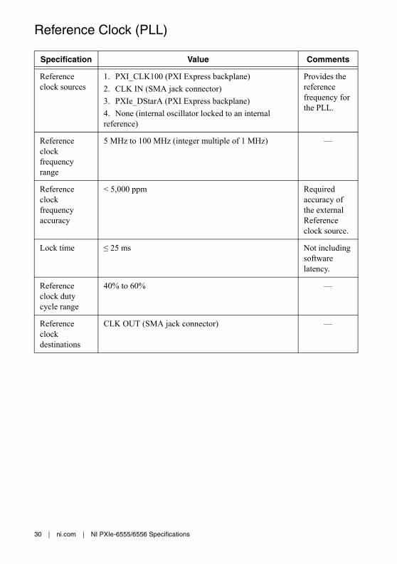
Reference Clock (PLL)
Specification Value Comments
Reference clock sources
1. PXI_CLK100 (PXI Express backplane)
2. CLK IN (SMA jack connector)
3. PXIe_DStarA (PXI Express backplane)
4. None (internal oscillator locked to an internal reference)
Provides the reference frequency for the PLL.
Reference clock frequency range
5 MHz to 100 MHz (integer multiple of 1 MHz) —
Reference clock frequency accuracy
< 5,000 ppm Required accuracy of the external Reference clock source.
Lock time ≤ 25 ms Not including software latency.
Reference clock duty cycle range
40% to 60% —
Reference clock destinations
CLK OUT (SMA jack connector) —

NI PXIe-6555/6556 Specifications | © National Instruments | 31
Waveform Specifications
Memory and Scripting
Specification Value Comments
Memory architecture
The NI 6555/6556 uses the Synchronization and Memory Core (SMC) technology in which waveforms and instructions share onboard memory. Parameters such as number of script instructions, maximum number of waveforms in memory, and number of samples available for waveform storage are flexible and user-defined.
Refer to the Onboard Memory section in the NI Digital Waveform Generator/Analyzer Help for more information.
Onboard memory size (generation)
NI 6555/NI 6556 NI 6556 Only Maximum limit for generation sessions assumes no scripting instructions.
8 Mbit/channel 64 Mbit/channel
Onboard memory size (acquisition)
8 Mbit/channel 64 Mbit/channel —
Generation modes Single-waveform mode:Generate a single waveform once, n times, or continuously.
—
Scripted mode:Generate a simple or complex sequence of waveforms. Use scripts to describe the waveforms to be generated, the order in which the waveforms are generated, how many times the waveforms are generated, and how the device responds to Script triggers.
32 | ni.com | NI PXIe-6555/6556 Specifications
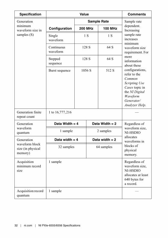
Generation minimum waveform size in samples (S)
Configuration
Sample Rate Sample rate dependent. Increasing sample rate increases minimum waveform size requirement. For more information about these configurations, refer to the Common Scripting Use Cases topic in the NI Digital Waveform Generator/Analyzer Help.
200 MHz 100 MHz
Single waveform
1 S 1 S
Continuous waveform
128 S 64 S
Stepped sequence
128 S 64 S
Burst sequence 1056 S 512 S
Generation finite repeat count
1 to 16,777,216 —
Generation waveform quantum
Data Width = 4 Data Width = 2 Regardless of waveform size, NI-HSDIO allocates waveforms in blocks of physical memory.
1 sample 2 samples
Generation waveform block size (in physical memory)
Data width = 4 Data width = 2
32 samples 64 samples
Acquisition minimum record size
1 sample Regardless of waveform size, NI-HSDIO allocates at least 640 bytes for a record.
Acquisition record quantum
1 sample —
Specification Value Comments

NI PXIe-6555/6556 Specifications | © National Instruments | 33
Acquisition maximum number of records
2,147,483,647 Session should fetch fast enough so that unfetched data is not overwritten.
Acquisition number of pre-Reference trigger samples
0 up to full record —
Acquisition number of post-Reference trigger samples
0 up to full record —
Hardware compare error FIFO depth
4,094 —
Hardware compare number of unique enable states
255 —
Hardware compare maximum speed
200 MHz —
Specification Value Comments

34 | ni.com | NI PXIe-6555/6556 Specifications
Triggers (Inputs to the NI 6556)
Specification Value Comments
Trigger types 1. Start trigger
2. Pause trigger
3. Script trigger <0..3> (generation sessions only)
4. Reference trigger (acquisition sessions only)
5. Advance trigger (acquisition sessions only)
6. Stop Trigger (generation sessions only)
—
Sources 1. PFI 0 (SMA jack connector)
2. PFI <1..3> (DDC connector)
3. PFI <24..31> (DDC connector)
4. PXI_TRIG<0..7> (PXI Express backplane)
5. Pattern match (acquisition sessions only)
6. Software (user function call)
7. Disabled (do not wait for a trigger)
—
Trigger detection
1. Start trigger (edge detection: rising or falling)
2. Pause trigger (level detection: high or low)
3. Script trigger <0..3> (edge detection: rising or falling; level detection: high or low)
4. Reference trigger (edge detection: rising or falling)
5. Advance trigger (edge detection: rising or falling)
6. Stop Trigger (edge detection: rising or falling)
—
Minimum required trigger pulse width
15 ns Typical. Only applies to Digital Edge Triggers.
Destinations 1. PFI 0 (SMA jack connectors)
2. PFI <1..3> (DDC connector)
3. PFI <24..31> (DDC connector)
4. PXI_TRIG<0..6> (PXI Express backplane)
Each trigger can be routed to any destination except the Pause trigger. The Pause trigger cannot be exported.

NI PXIe-6555/6556 Specifications | © National Instruments | 35
Events (Generated from the NI 6556)
Trigger rearm time Start to
Reference Trigger
Start to Advance Trigger
Advance to
Advance Trigger
Reference to
Reference Trigger
Maximum number of samples.
150 S 220 S 220 S 220 S
Delay from Pause trigger to Pause state and Stop trigger to Done state
Generation Sessions Acquisition Sessions Maximum; Use the Data Active event during generation to determine on a sample by sample basis when the device enters the Pause or Done states.
55 Sample Clock periods + 300 ns
Synchronous with the data.
Delay from trigger to digital data output
6 Sample Clock periods + 600 ns Maximum; Start trigger and Script triggers.
Specification Value Comments
Event type 1. Marker <0..2> (generation sessions only)
2. Data Active event (generation sessions only)
3. Ready for Start event
4. Ready for Advance event (acquisition sessionsonly)
5. End of Record event (acquisition sessions only)
—
Specification Value Comments

36 | ni.com | NI PXIe-6555/6556 Specifications
Miscellaneous
Power
Destinations 1. PFI 0 (SMA jack connectors)
2. PFI <1..3> (DDC connector)
3. PFI <24..31> (DDC connector)
4. PXI_TRIG<0..6> (PXI Express backplane)
Each event can be routed to any destination, except the Data Active event. The Data Active event can only be routed to the PFI channels.
Marker time resolution (placement)
Markers can be placed at any sample. —
Specification Value Comments
Warm-up time 30 minutes From driver loaded.
External calibration interval
1 year —
Specification 12 V 3.3 V Total Power Comments
Maximum allowed current
5.2 A 5.7 A — Maximum allowed power before device shut down requiring reset of the device.Maximum
allowed device power
— — 76 W
Specification Value Comments

NI PXIe-6555/6556 Specifications | © National Instruments | 37
Physical
I/O Panel Connectors
3.3 V swing at 200 Mbps
4.5 A 4.1 A 67.5 W Typical results are commensurate with an aggressive user application using all data channels into a high-impedance load with active loads disabled (unless otherwise noted) across temperature.
5.0 V swing at 100 Mbps
4.3 A 4.0 A 64.8 W
8.0 V swing at 50 Mbps
4.3 A 3.8 A 64.1 W
3.3 V swing at 100 Mbps with Active Load set to 24 mA
4.7 A 4.5 A 71.5 W
Specification Value Comments
Dimensions 21.6 × 2.0 × 13.0 cm
Dual 3U CompactPCI Express slot; PXI Express compatible
—
Weight 28 oz (793 g) —
Label Function(s)Connector
Type
CLK IN External Sample clock, external Reference clock. SMA jack
PFI 0 Events, triggers. SMA jack
CLK OUT External Sample clock, exported Reference clock. SMA jack
AUX I/O External force, external sense, and analog calibration.
Note: Supported on the NI 6556 only.
Combicon
Digital Data & Control (DDC)
Digital data channels, PPMU channels, exported Sample clock, STROBE, events, triggers.
68-pin VHDCI
REMOTE SENSE
PPMU remote sensing channels, external force, external sense, and analog calibration.
68-pin VHDCI
Specification 12 V 3.3 V Total Power Comments

38 | ni.com | NI PXIe-6555/6556 Specifications
Software
Environment
Note To ensure that the NI 6555/6556 cools effectively, follow the guidelines in the Maintain Forced Air Cooling Note to Users included with the NI 6555/6556. The NI 6555/6556 is intended for indoor use only.
Specification Value Comments
Driver software NI-HSDIO driver software 1.8.1 or later for the NI 6556; NI-HSDIO 1.9 for the NI 6555. NI-HSDIO allows you to configure and control the NI 6555/6556. NI-HSDIO provides application interfaces for many development environments. NI-HSDIO follows IVI application programming interface (API) guidelines.
—
Application software
NI-HSDIO provides programming interfaces for the following application development environments (ADEs):
• National Instruments LabVIEW
• National Instruments LabWindows™/CVI™
• Microsoft Visual C/C++
Refer to the NI-HSDIO Readme for more information about supported ADE versions.
Test panel National Instruments Measurement & Automation Explorer (MAX) provides test panels with basic acquisition and generation functionality for the NI 6555/6556. MAX is included on the NI-HSDIO driver media.
—
Specification Value Comments
Operating temperature
0 to +45 ºC in all NI PXI Express and hybrid NI PXI Express chassis. (Meets IEC 60068-2-2.)
—
Operating relative humidity
10% to 90% relative humidity, noncondensing (Meets IEC 60068-2-56.)
—
Altitude 2,000 m at 25 ºC ambient temperature —
Pollution Degree
2 —

NI PXIe-6555/6556 Specifications | © National Instruments | 39
Safety
Caution The protection provided by the NI PXIe-6555/6556 can be impaired if it is used in a manner not described in this document.
This product meets the requirements of the following standards of safety for electrical equipment for measurement, control, and laboratory use:
• IEC 61010-1, EN 61010-1
• UL 61010-1, CSA 61010-1
Note For UL and other safety certifications, refer to the product label or the Online Product Certification section.
Electromagnetic CompatibilityThis product meets the requirements of the following EMC standards for electrical equipment for measurement, control, and laboratory use:
• EN 61326-1 (IEC 61326-1): Class A emissions; Basic immunity
• EN 55011 (CISPR 11): Group 1, Class A emissions
• AS/NZS CISPR 11: Group 1, Class A emissions
• FCC 47 CFR Part 15B: Class A emissions
• ICES-001: Class A emissions
Storage temperature
-20 to +70 ºC (Meets IEC-60068-2-2.)
—
Storage relative humidity
5% to 95% relative humidity, noncondensing (Meets IEC 60068-2-56.)
—
Operating shock
30 g, half-sine, 11 ms pulse (Meets IEC 60068-2-27. Test profile developed in accordance with MIL-PRF-28800F.)
—
Storage shock 50 g, half-sine, 11 ms pulse (Meets IEC 60068-2-27. Test profile developed in accordance with MIL-PRF-28800F.)
—
Operating vibration
5 Hz to 500 Hz, 0.3 grms (Meets IEC 60068-2-64.)
—
Storage vibration
5 Hz to 500 Hz, 2.46 grms (Meets IEC 60068-2-64. Test profile exceeds requirements of MIL-PRF-28800F, Class B.)
—
Specification Value Comments

40 | ni.com | NI PXIe-6555/6556 Specifications
Note In the United States (per FCC 47 CFR), Class A equipment is intended for use in commercial, light-industrial, and heavy-industrial locations. In Europe, Canada, Australia, and New Zealand (per CISPR 11) Class A equipment is intended for use only in heavy-industrial locations.
Note Group 1 equipment (per CISPR 11) is any individual, scientific, or medical equipment that does not intentionally generate radio frequency energy for the treatment of material or inspection/analysis purposes.
Note For EMC declarations and certifications, refer to the Online Product Certification section of this document.
CE ComplianceThis product meets the essential requirements of applicable European Directives as follows:
• 2006/95/EC; Low-Voltage Directive (safety)
• 2004/108/EC; Electromagnetic Compatibility Directive (EMC)
Online Product CertificationTo obtain product certifications and the Declaration of Conformity for this product, visit ni.com/certification, search by model number or product line, and click the appropriate link in the Certification column.
Environmental ManagementNI is committed to designing and manufacturing products in an environmentally responsible manner. NI recognizes that eliminating certain hazardous substances from our products is beneficial to the environment and to NI customers.
For additional environmental information, refer to the Minimize Our Environmental Impact web page at ni.com/environment. This page contains the environmental regulations and directives with which NI complies, as well as other environmental information not included in this document.
Waste Electrical and Electronic Equipment (WEEE)EU Customers At the end of the product life cycle, all products must be sent to a WEEE recycling center. For more information about WEEE recycling centers, National Instruments WEEE initiatives, and compliance with WEEE Directive 2002/96/EC on Waste and Electronic Equipment, visit ni.com/environment/weee.

NI PXIe-6555/6556 Specifications | © National Instruments | 41
Where to Go for SupportThe National Instruments website is your complete resource for technical support. At ni.com/support you have access to everything from troubleshooting and application development self-help resources to email and phone assistance from NI Application Engineers.
Visit ni.com/services for NI Factory Installation Services, repairs, extended warranty, and other services.
Visit ni.com/register to register your National Instruments product. Product registration facilitates technical support and ensures that you receive important information updates from NI.
A Declaration of Conformity (DoC) is our claim of compliance with the Council of the European Communities using the manufacturer’s declaration of conformity. This system affords the user protection for electromagnetic compatibility (EMC) and product safety. You can obtain the DoC for your product by visiting ni.com/certification. If your product supports calibration, you can obtain the calibration certificate for your product at ni.com/calibration.
National Instruments corporate headquarters is located at 11500 North Mopac Expressway, Austin, Texas, 78759-3504. National Instruments also has offices located around the world. For telephone support in the United States, create your service request at ni.com/support or dial 512 795 8248. For telephone support outside the United States, visit the Worldwide Offices section of ni.com/niglobal to access the branch office websites, which provide up-to-date contact information, support phone numbers, email addresses, and current events.
RoHSNational Instruments
(RoHS) National Instruments RoHS ni.com/environment/rohs_china (For information about China RoHS compliance, go to ni.com/environment/rohs_china.)

© 2011–2013 National Instruments. All rights reserved.
375749G Sep13
Refer to the NI Trademarks and Logo Guidelines at ni.com/trademarks for more information on National Instruments trademarks. Other product and company names mentioned herein are trademarks or trade names of their respective companies. For patents covering National Instruments products/technology, refer to the appropriate location: Help»Patents in your software, the patents.txt file on your media, or the National Instruments Patents Notice at ni.com/patents. You can find information about end-user license agreements (EULAs) and third-party legal notices in the readme file for your NI product. Refer to the Export Compliance Information at ni.com/legal/export-compliance for the National Instruments global trade compliance policy and how to obtain relevant HTS codes, ECCNs, and other import/export data.