new approaches to harness global...
TRANSCRIPT

ASPDAC'01 Tutorial Jason Cong 1
PART V
New Approaches to Harness Global Interconnects
Jason Cong Computer Science Department
University of California at Los AngelesEmail: [email protected]
Tel: 310-206-2775http://cadlab.cs.ucla.edu/~cong

ASPDAC'01 Tutorial Jason Cong 2
Part V Outline
nn InterconnectInterconnect--Centric Design FlowCentric Design Flownn Interconnect Performance Estimation ModelsInterconnect Performance Estimation Models
uu IPEM for optimal IPEM for optimal wiresizingwiresizinguu IPEM for IPEM for wiresizing wiresizing and buffer insertionand buffer insertion
nn Interconnect PlanningInterconnect Planninguu Physical hierarchy generationPhysical hierarchy generationuu FloorplanFloorplan/coarse placement with interconnect planning/coarse placement with interconnect planninguu Interconnect architecture planningInterconnect architecture planning
nn Concluding RemarksConcluding Remarks

ASPDAC'01 Tutorial Jason Cong 3
Clock cycles required for traveling 2cm line under BIWS
(buffer insertion and wire sizing)
1 G
Hz
3 G
Hz
5 G
Hz
0.07
um
0.10
um
0.13
um
0.18
ym
0.25
um
0
1
2
3
4
5
cloc
k cy
cle(
s)
Estimated by IPEMOn NTRS’97 technology
Driver size: 100x min gateReceiver size: 100x min gateBuffer size: 100x min gate

ASPDAC'01 Tutorial Jason Cong 4
How Far Can We Go in Each Clock Cycle
7.52 15.04 22.56 24.9 (mm)0
1 clock 2 clock 3 clock
4 clock
5 clock
6 clock
7 clock n NTRS’97 0.07um Techn 5 G Hz across-chip clockn 620 mm2 (24.9mm x
24.9mm)n IPEM BIWS estimations
u Buffer size: 100xu Driver/receiver size: 100x
n From corner to corner:u 7 clock cycles

ASPDAC'01 Tutorial Jason Cong 5
Two Important Implications
nn Interconnects determine the system Interconnects determine the system performanceperformance
nn Need multiple clock cycles to cross the global Need multiple clock cycles to cross the global interconnects in interconnects in gigagiga--hertz designshertz designs
Interconnect/communication-centric design methodology
Pipelining/retiming on global interconnects

ASPDAC'01 Tutorial Jason Cong 6
Interconnect-Centric Design Methodology
deviceinterconnect
device interconnect
ProgramsData/Objects
Programs Data/Objects
nn Proposed transitionProposed transition
nn Analogy Analogy
device/function centric interconnect/communication centric

ASPDAC'01 Tutorial Jason Cong 7
Interconnect-Centric IC Design Flow Under Development at UCLA
Architecture/Conceptual-level Design
Design Specification
Final Layout
abstractionStructure viewFunctional viewPhysical viewTiming view
HDM
Synthesis and Placement under Physical Hierarchy
Interconnect Planning•Physical Hierarchy Generation•Foorplan/Coarse Placement with Interconnect Planning•Interconnect Architecture Planning
Interconnect Optimization(TRIO)
• Topology Optimization with Buffer Insertion• Wire sizing and spacing• Simultaneous Buffer Insertion and Wire Sizing• Simultaneous Topology Construction
with Buffer Insertion and Wire Sizing
Interconnect LayoutRoute Planning
Point-to-Point Gridless Routing
Interconnect PerformanceEstimation Models (IPEM)
•OWS, SDWS, BISWS
Interconnect SynthesisPerformance-driven Global Routing
Pseudo Pin Assignment under Noise Control
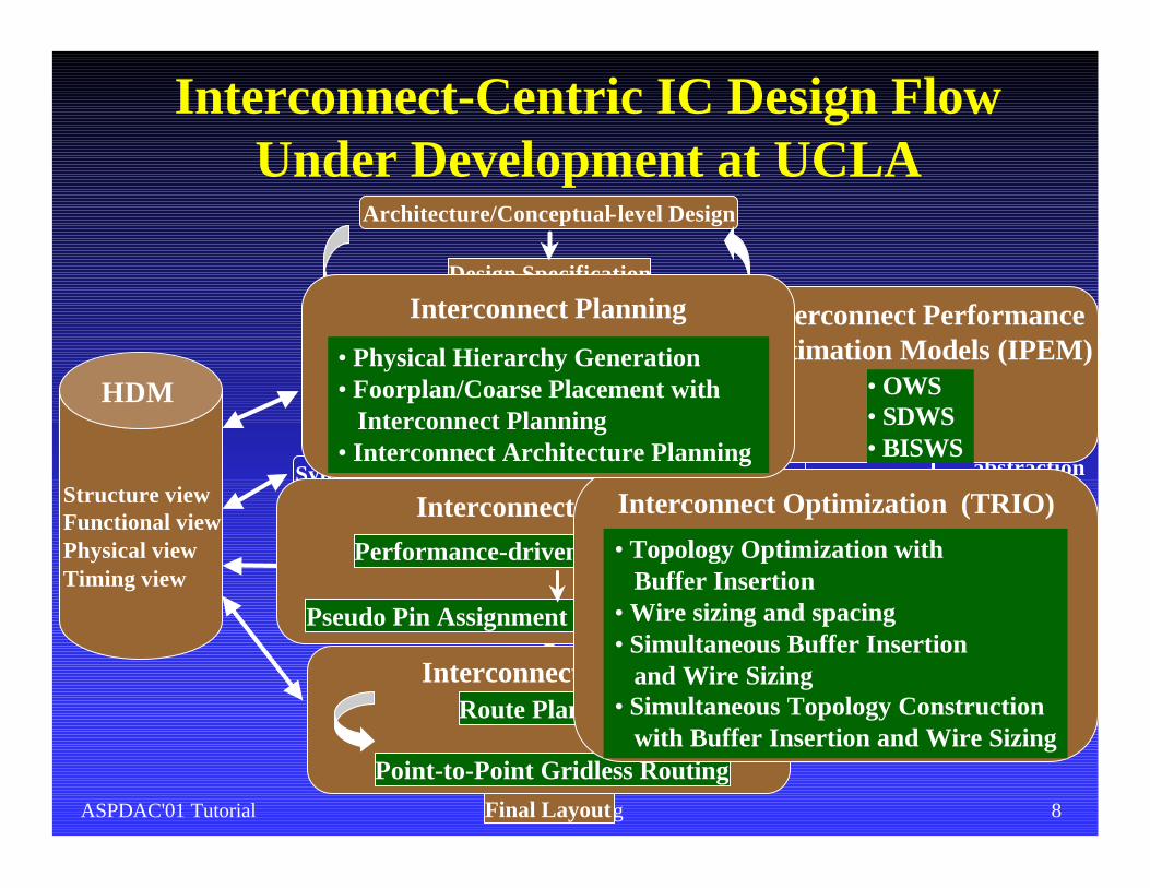
ASPDAC'01 Tutorial Jason Cong 8
Interconnect-Centric IC Design Flow Under Development at UCLA
Architecture/Conceptual-level Design
Design Specification
Final Layout
abstractionStructure viewFunctional viewPhysical viewTiming view
HDM
Synthesis and Placement under Physical Hierarchy
Interconnect Planning•Physical Hierarchy Generation•Foorplan/Coarse Placement with Interconnect Planning•Interconnect Architecture Planning
Interconnect Optimization(TRIO)
• Topology Optimization with Buffer Insertion• Wire sizing and spacing• Simultaneous Buffer Insertion and Wire Sizing• Simultaneous Topology Construction
with Buffer Insertion and Wire Sizing
Interconnect LayoutRoute Planning
Point-to-Point Gridless Routing
Interconnect PerformanceEstimation Models (IPEM)
•OWS, SDWS, BISWS
Interconnect SynthesisPerformance-driven Global Routing
Pseudo Pin Assignment under Noise Control
Interconnect SynthesisPerformance-driven Global Routing
Pseudo Pin Assignment under Noise Control
Interconnect LayoutRoute Planning
Point-to-Point Gridless Routing
Interconnect PerformanceEstimation Models (IPEM)
• OWS• SDWS• BISWS
Interconnect Optimization (TRIO)• Topology Optimization with
Buffer Insertion• Wire sizing and spacing• Simultaneous Buffer Insertion
and Wire Sizing• Simultaneous Topology Construction
with Buffer Insertion and Wire Sizing
Interconnect Planning
• Physical Hierarchy Generation• Foorplan/Coarse Placement with
Interconnect Planning• Interconnect Architecture Planning

ASPDAC'01 Tutorial Jason Cong 9
Interconnect-Centric IC Design Flow Under Development at UCLA
Architecture/Conceptual-level Design
Design Specification
Final Layout
abstractionStructure viewFunctional viewPhysical viewTiming view
HDM
Synthesis and Placement under Physical Hierarchy
Interconnect Planning•Physical Hierarchy Generation•Foorplan/Coarse Placement with Interconnect Planning•Interconnect Architecture Planning
Interconnect Optimization(TRIO)
• Topology Optimization with Buffer Insertion• Wire sizing and spacing• Simultaneous Buffer Insertion and Wire Sizing• Simultaneous Topology Construction
with Buffer Insertion and Wire Sizing
Interconnect LayoutRoute Planning
Point-to-Point Gridless Routing
Interconnect PerformanceEstimation Models (IPEM)
•OWS, SDWS, BISWS
Interconnect SynthesisPerformance-driven Global Routing
Pseudo Pin Assignment under Noise Control

ASPDAC'01 Tutorial Jason Cong 10
Part V Outline
nn InterconnectInterconnect--Centric Design FlowCentric Design Flownn Interconnect Performance Estimation ModelsInterconnect Performance Estimation Models
uu IPEM for optimal IPEM for optimal wiresizingwiresizinguu IPEM for IPEM for wiresizing wiresizing and buffer insertionand buffer insertion
nn Interconnect PlanningInterconnect Planninguu Physical hierarchy generationPhysical hierarchy generationuu FloorplanFloorplan/coarse placement with interconnect /coarse placement with interconnect
planningplanninguu Interconnect architecture planningInterconnect architecture planning
nn Concluding RemarksConcluding Remarks
ASPDAC'01 Tutorial Jason Cong 11
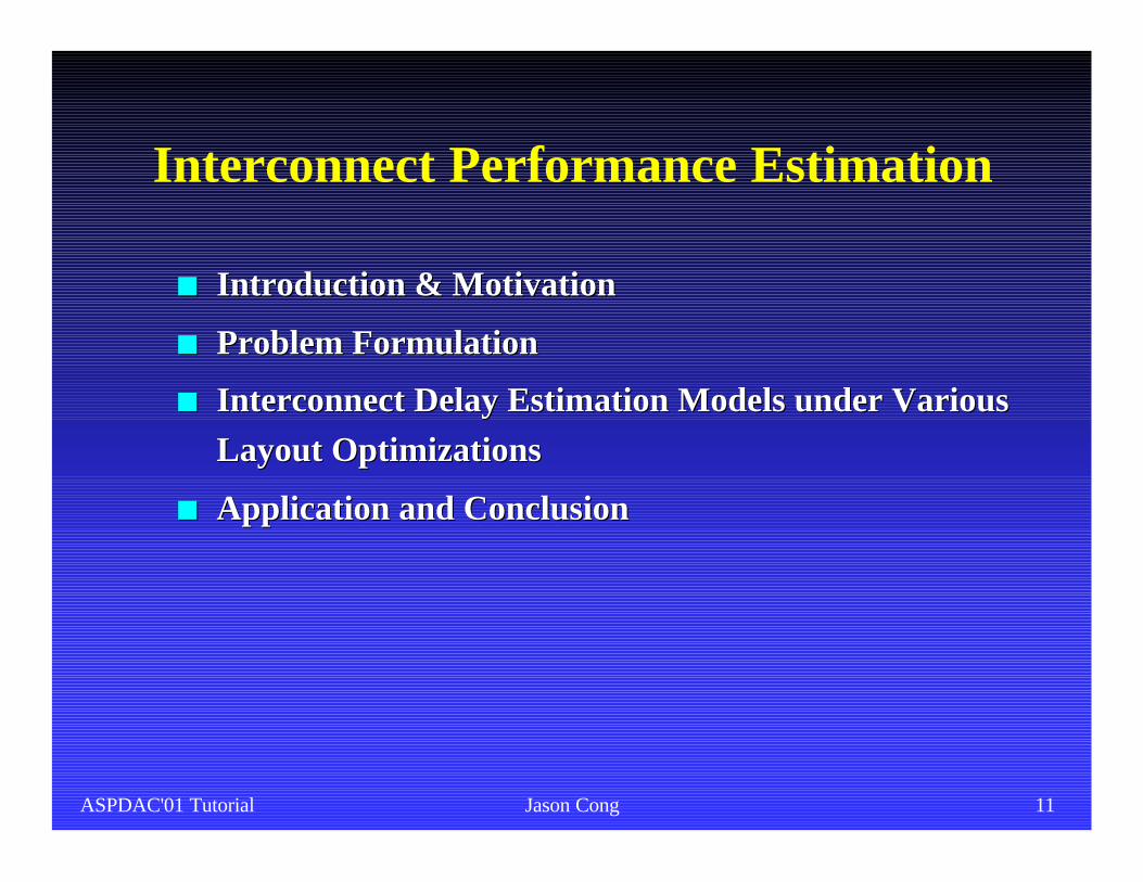
Interconnect Performance Estimation
nn Introduction & MotivationIntroduction & Motivation
nn Problem FormulationProblem Formulation
nn Interconnect Delay Estimation Models under Various Interconnect Delay Estimation Models under Various Layout OptimizationsLayout Optimizations
nn Application and ConclusionApplication and Conclusion

ASPDAC'01 Tutorial Jason Cong 12
Impact of Interconnect Optimization on Future Technology Generations
0
0.5
1
1.5
2
2.5
3
3.5
4
4.5
5
0.25 0.18 0.15 0.13 0.1 0.07
Technology (um)
Del
ay (n
s)
2cm DS
2cm BIS
2cm BISWS
l DS: Driver Sizing only
l BIS: Buffer Insertion and Sizing
l BISWS: Simultaneous Buffer Insertion/Sizing and Wiresizing

ASPDAC'01 Tutorial Jason Cong 13
Complexity of Existing Interconnect Opt. Algorithms
nn 2cm line, W=20, B=10, segment every 500um2cm line, W=20, B=10, segment every 500umnn Use Use best availablebest available algorithms: algorithms:
uu Local Refinement (Local Refinement (LRLR) ) uu Dynamic Programming (Dynamic Programming (DPDP) ) uu Hybrid of Hybrid of DP+LRDP+LR
Algorithm OWS BI+OWS BIWS BISWS
Delay (ns) 4.5 1.6 1.02 0.81
CPU (s) 0.06 0.42 4.5 12.4
LR DPDP+LR
( HSPICE needs( HSPICE needs additional 60 seconds! )additional 60 seconds! )

ASPDAC'01 Tutorial Jason Cong 14
Needs for Efficient Interconnect Estimation Models
nn EfficiencyEfficiency
nn AbstractionAbstraction to hide detailed design informationto hide detailed design informationuu granularity of wire segmentationgranularity of wire segmentation
uu number of wire widths, buffer sizes, ...number of wire widths, buffer sizes, ...
nn Explicit relationExplicit relation to enable optimal design decision at to enable optimal design decision at high levelshigh levels
nn Ease of interactionEase of interaction with logic/high level synthesis toolswith logic/high level synthesis tools

ASPDAC'01 Tutorial Jason Cong 15
nn Develop a set of Develop a set of interconnect performance estimation interconnect performance estimation modelsmodels ((IPEMIPEM), under different optimization alternatives:), under different optimization alternatives:uu Optimal Wire Sizing Optimal Wire Sizing (OWS)(OWS)uu Simultaneous Driver and Wire Sizing Simultaneous Driver and Wire Sizing (SDWS)(SDWS)uu Simultaneous Buffer Insertion and Wire Sizing Simultaneous Buffer Insertion and Wire Sizing (BIWS)(BIWS)uu Simultaneous Buffer Insertion/Sizing and Wire Sizing Simultaneous Buffer Insertion/Sizing and Wire Sizing (BISWS)(BISWS)
nn IPEM haveIPEM haveuu closedclosed--form formula or simple characteristic equationsform formula or simple characteristic equationsuu constant running time in practiceconstant running time in practiceuu high accuracy (about 90% accuracy on average)high accuracy (about 90% accuracy on average)
Interconnect Performance Estimation Modeling
[Cong-Pan, ASPDAC’99, TAU’99, DAC’99]

ASPDAC'01 Tutorial Jason Cong 16
nn RRd0d0 driver effective resistance of the input stage driver effective resistance of the input stage GG00nn RRdd driver effective resistance of driver effective resistance of GGnn ll interconnect wire lengthinterconnect wire lengthnn CCLL loading capacitanceloading capacitance
G
Input
G0l
CL
What is the optimized delay?Do not run TRIO or other optimization tools !
Problem Formulation

ASPDAC'01 Tutorial Jason Cong 17
nn InterconnectInterconnectuu ccaa area capacitance coefficientarea capacitance coefficientuu ccff fringing capacitance coefficientfringing capacitance coefficientuu rr sheet resistancesheet resistance
nn DeviceDeviceuu ttgg intrinsic gate delayintrinsic gate delayuu ccgg input capacitance of the minimum gateinput capacitance of the minimum gateuu rrgg output resistance of the minimum gateoutput resistance of the minimum gate
nn Based on 1997 National Technology Roadmap for Based on 1997 National Technology Roadmap for Semiconductors (NTRS’97)Semiconductors (NTRS’97)
Parameters and Notations

ASPDAC'01 Tutorial Jason Cong 18
nn ClosedClosed--formform delay estimation formuladelay estimation formula
llcrcRcRlW
llW
lClRT fadfdLdows ⋅
++= +
)(2
)(),,(
2
1
22
1
αα
αα
where
arc41
1 =αLd
a
CRrc
21
2 =α,
W(x) is Lambert’s W function defined as we xw =
nn ClosedClosed--formform area estimation formulaarea estimation formula
lcR
ClcrClRAad
LfLdows ⋅+=
2)2(),,(
Delay/Area Estimation under OWS

ASPDAC'01 Tutorial Jason Cong 19
nn Theorem: Theorem: TTowsows is a subis a sub--quadratic, convex function of quadratic, convex function of length length l l
nn Note: Without Note: Without wiresizingwiresizing, wiring delay , wiring delay ∝∝ ll22, , as used in as used in some previous layoutsome previous layout--driven logic synthesis systems, driven logic synthesis systems, such as [such as [RamachandranRamachandran et al., ICCADet al., ICCAD--92], is no 92], is no longer accurate!longer accurate!
nn ClosedClosed--form DEMform DEM--OWS will serve as a basis for OWS will serve as a basis for deriving SDWS, BIWS and BISWSderiving SDWS, BIWS and BISWS
Property of DEM-OWS

ASPDAC'01 Tutorial Jason Cong 20
Delay modeling
0.00
0.10
0.20
0.30
0.40
0.50
0.60
0.70
0.80
0.90
1.00
0 2000 4000 6000 8000 10000 12000 14000 16000
length(um)
ns
Model
TRIO
Comparison of IPEM-OWS vs. TRIO
n 0.18um, Rd = rg /100, CL = cg x 100
n For expt., max wire width is 20x min, wire is segmented in every 10um

ASPDAC'01 Tutorial Jason Cong 21
Area Estimation for OWS
0
0.5
1
1.5
2
0 4000 8000 12000 16000 20000
length(um)
width(um)Model TRIO

ASPDAC'01 Tutorial Jason Cong 22
{ }LbowsgbdowsLdbiws ClRTtClRTClRT ,)1(,(),,(min10
),,(1 ααα
−++≤≤
=
),,( Ldows ClRT
Solve for l, => critical length lcrit(b, Rd , CL )
- Computed by bisection method
- Constant time in practice CL
1 best buffer
αl (1-α)l
bdR
CL
RdNo buffer
l
Critical Length for BI under OWS

ASPDAC'01 Tutorial Jason Cong 23
Technology (um) 0.25 0.18 0.15 0.13 0.10 0.07b=10x 4.12 3.80 3.97 3.61 2.92 2.08b=50x 6.40 5.81 6.01 5.51 4.45 3.30
b=100x 7.47 6.83 7.04 6.39 5.30 3.91b=200x 8.65 7.92 8.14 7.43 6.35 4.49b=500x 9.98 9.10 9.30 8.57 7.13 5.21
Decrease
unit: mm
- Cf. [Otten ISPD’98, Otten-Brayton DAC’98] (uniform wire width)
Min. WS 2.52 2.23 2.14 1.94 1.50 1.43
- Denote lc = lcrit (b, Rb , Cb)
Critical Lengths lcrit (b, Rb , Cb)

ASPDAC'01 Tutorial Jason Cong 24
“Logic Volume” within lc
Technology (um) 0.25 0.18 0.15 0.13 0.10 0.07
2-NAND (um2)7.80 4.04 3.00 2.18 1.28 0.64
b=10x 0.55 0.89 1.31 1.49 1.66 1.69b=50x 1.31 2.09 3.01 3.48 3.87 4.25
b=100x 1.79 2.88 4.13 4.68 5.48 5.97b=200x 2.4 3.88 5.52 6.33 7.87 7.88b=500x 3.19 5.12 7.21 8.42 9.93 10.6
Increase
- Defined as the number of min 2-input NAND gates that can be packed within the area of lc/2 * lc/2
unit: million

ASPDAC'01 Tutorial Jason Cong 25
Property of BIWS
CL
b b bb
lc lc lc llast
nn Theorem:Theorem: For BIWS, the distances between adjacent For BIWS, the distances between adjacent buffers are the same, and equal tobuffers are the same, and equal to llcc ---- the critical the critical length.length.
nn ProofProof: based on the convexity of : based on the convexity of TTowsows

ASPDAC'01 Tutorial Jason Cong 26
IPEM for BIWS
gbiwsbiws tlT +⋅τ=
biwsτ is the slope, and can be obtained from Tows(Rb , lc, Cb)
nn Original long interconnect is divided into Original long interconnect is divided into ll//llcc stagestagenn The The stage numberstage number is proportional to is proportional to llnn Each stage of length Each stage of length llcc has delay has delay TTowsows((RRbb , , llcc, , CCbb))èè Linear DEM for BIWSLinear DEM for BIWS

ASPDAC'01 Tutorial Jason Cong 27
IPEM for BIWS vs. TRIODelay Modeling
0
0.2
0.4
0.6
0.8
1
0 4000 8000 12000 16000 20000
length(um)
ns
Model TRIO
n 0.18um, Rd0 = rg /10, CL = cg x 10, buffer type is 100 x min.n For expt., max. wire width is 20x min. width, wire is segmented in every
100um.

ASPDAC'01 Tutorial Jason Cong 28
IPEM under BISWSnn Observations from Observations from extensiveextensive experiments:experiments:
uu Linear delay versus lengthLinear delay versus lengthuu Internal buffers are about the same sizeInternal buffers are about the same size
nn Therefore, we estimate BISWS by the best BIWS from Therefore, we estimate BISWS by the best BIWS from available buffer typesavailable buffer types
gbiswsbisws tlT +⋅τ =biwsbisws
Bbττ
∈= minwhere , B is the buffer set
nn Linear delay model for optimal BISWSLinear delay model for optimal BISWS
nn Complexity O(|Complexity O(|BB|). Since the set |). Since the set BB is normally is normally less than 20, constant time in practice.less than 20, constant time in practice.

ASPDAC'01 Tutorial Jason Cong 29
Comparison of IPEM for BISWS vs. TRIODelay Modeling
0
0.2
0.4
0.6
0.8
0 4000 8000 12000 16000 20000
length(um)
nsModel TRIO
n 0.18um, Rd0 = rg /10, CL = cg x 10n For expt., max. allowable buffer/driver size is 400x min device; max. wire
width is 20x min. width; wire is segmented in every 100um.

ASPDAC'01 Tutorial Jason Cong 30
IPEM for Multiple-Pin Nets
n Estimation with different optimization objectives:u Minimize the delay to a single critical sink (SCS)u Minimize the maximum delay (defined as the tree delay) for
multiple critical sinks (MCS)u Minimize weighted delay ...
G
Input
G0
Csn
Cs2
Cs1
Sn
S1
S2
S3
Cs3

ASPDAC'01 Tutorial Jason Cong 31
Some Applications of IPEM
nn LayoutLayout--driven physical and RTL level driven physical and RTL level floorplanningfloorplanninguu Predict accuratePredict accurate interconnect delay and routing resource interconnect delay and routing resource
without really going into layout details;without really going into layout details;uu Use accurate interconnect delay/area to guide Use accurate interconnect delay/area to guide
floorplanningfloorplanning/placement/placement
nn Interconnect Architecture PlanningInterconnect Architecture Planninguu E.g. Wire width planningE.g. Wire width planning
nn Floorplanning Floorplanning + interconnect planning+ interconnect planninguu E.g. Buffer block planningE.g. Buffer block planning
nn Available from Available from http://http://cadlabcadlab..cscs..uclaucla..eduedu/~cong/~cong

ASPDAC'01 Tutorial Jason Cong 32
Part V Outline
nn InterconnectInterconnect--Centric Design FlowCentric Design Flownn Interconnect Performance Estimation ModelsInterconnect Performance Estimation Models
uu IPEM for optimal IPEM for optimal wiresizingwiresizinguu IPEM for IPEM for wiresizing wiresizing and buffer insertionand buffer insertion
nn Interconnect PlanningInterconnect Planninguu Physical hierarchy generationPhysical hierarchy generationuu FloorplanFloorplan/coarse placement with interconnect planning/coarse placement with interconnect planninguu Interconnect architecture planningInterconnect architecture planning
nn Concluding RemarksConcluding Remarks

ASPDAC'01 Tutorial Jason Cong 33
Physical Hierarchy Generationnn Designs are hierarchical due to high complexityDesigns are hierarchical due to high complexitynn Design specification (in HDL) follows logic hierarchyDesign specification (in HDL) follows logic hierarchynn Logic hierarchy may not be suitable to be embedded Logic hierarchy may not be suitable to be embedded
on a 2D silicon surface, resulting poor interconnect on a 2D silicon surface, resulting poor interconnect designsdesignsuu RTRT--levellevel floorplanningfloorplanning is a bad idea!is a bad idea!
nn Solution: transform logic hierarchy to physical Solution: transform logic hierarchy to physical hierarchyhierarchy

ASPDAC'01 Tutorial Jason Cong 34
Example of Logic Hierarchy in Final Layout
By courtesy of IBM (Tony Drumm)

ASPDAC'01 Tutorial Jason Cong 35
Example of Logic Hierarchy in Final Layout
By courtesy of IBM (Tony Drumm)

ASPDAC'01 Tutorial Jason Cong 36
Transform Logic Hierarchy to Physical Hierarchy
nn Simultaneous partitioning, coarse placement, and Simultaneous partitioning, coarse placement, and retiming on the retiming on the flatflat netlistnetlist to generate a good physical to generate a good physical hierarchyhierarchyuu Synthesis will followSynthesis will follow
nn Use multiUse multi--level optimization to handle with the level optimization to handle with the complexitycomplexity

ASPDAC'01 Tutorial Jason Cong 37
nn Importance of Partitioning:Importance of Partitioning:uu Conventional view: enables divideConventional view: enables divide--andand--conquerconqueruu DSM view: DSM view: defines global and local interconnectsdefines global and local interconnects
D >> d !!!
Local Interconnect d
Global Interconnect D
Role of Partitioning

ASPDAC'01 Tutorial Jason Cong 38
Need of Considering Retiming during Partitioning- Retiming/pipelining on global interconnects
nn Multiple clock cycles are needed to cross the chipMultiple clock cycles are needed to cross the chip
nn Proper partitioning allows retiming to Proper partitioning allows retiming to hidehide global global interconnect delays.interconnect delays.
same cutsize
f (A) = 8
Partitioning A
f (B) = 8
Partitioning B
f (B) = 8f (A) = 6

ASPDAC'01 Tutorial Jason Cong 39
Sequential Arrival Time (SAT)nn Definition Definition [Pan et al, TCAD98][Pan et al, TCAD98]
uu ll((vv) = max delay from PIs to ) = max delay from PIs to vv after opt. retiming under a given clock after opt. retiming under a given clock period period ff
uu ll((vv) = max{) = max{ll((uu) ) -- ff ·· ww((u,vu,v) + ) + dd((u,vu,v) + ) + dd((vv)})}
uu Relation to retiming: Relation to retiming: rr((vv) = ) = ll((vv) / ) / ff -- 11uu Theorem: Theorem: PP can be retimed to can be retimed to ff + max{+ max{dd((ee)} iff )} iff ll(POs) (POs) ≤≤ ff
u
wv
l(u) = 7
l(w) = 3
d(v) = 1, d(e) = 2, f = 5l(v) = max{7-5·1+2+1, 3+2+1} = 6
u v
l(u) w(u,v) d(v)

ASPDAC'01 Tutorial Jason Cong 40
nn Minimize SAT during partitioning/placementMinimize SAT during partitioning/placementnn Apply optimal retiming to the resulting solution (best Apply optimal retiming to the resulting solution (best
suitable for retiming)suitable for retiming)nn Partitioning/placement with retiming can be applied Partitioning/placement with retiming can be applied
recursively to generate physical hierarchyrecursively to generate physical hierarchynn Good news: SAT can be computed efficiently (linear Good news: SAT can be computed efficiently (linear
time in practice, quadratic time in the worst case)time in practice, quadratic time in the worst case)nn Difficulty: FlattenedDifficulty: Flattened netlistnetlist can be very large!can be very large!
uu Solution: use multiSolution: use multi--level methodlevel method
Simultaneous Partitioning/Placement with Retiming

ASPDAC'01 Tutorial Jason Cong 41
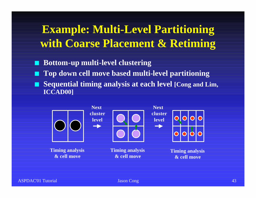
Multi-level Partitioning
Coarsening Uncoarsening &Refinement
Initial Partitioning
n Iterative coarsening (clustering) to generate a multi-level hierarchy
n Initial partitioning on the coarsest leveln Iterative de-clustering and refinement

ASPDAC'01 Tutorial Jason Cong 42
nn Hierarchical approach: higherHierarchical approach: higher--level design level design constrainsconstrains lowerlower--level designslevel designsuu Not sufficient information at higherNot sufficient information at higher--levelleveluu Mistake at higher level is impossible or costly to correctMistake at higher level is impossible or costly to correct
nn MultiMulti--level approach: finerlevel approach: finer--level design level design refinesrefinescoarsecoarse--level designlevel designuu Converge to better solution as more details are consideredConverge to better solution as more details are considered
Hierarchical Approach vs Multi-Level Approach
ASPDAC'01 Tutorial Jason Cong 43
Example: Multi-Level Partitioning with Coarse Placement & Retiming
Timing analysis& cell move
Timing analysis& cell move
Next clusterlevel
Timing analysis& cell move
Next clusterlevel
n Bottom-up multi-level clusteringn Top down cell move based multi-level partitioningn Sequential timing analysis at each level [Cong and Lim,
ICCAD00]

ASPDAC'01 Tutorial Jason Cong 44
Success of Multi-Level Approach
nn First used to solve partial differential equations (multiFirst used to solve partial differential equations (multi--grid method)grid method)
nn Successfully applied to circuit partitioning (Successfully applied to circuit partitioning (hMetis hMetis [[KarypisKarypis et al, 1997]et al, 1997]))uu BestBest partitionerpartitioner for cutfor cut--size minimizationsize minimization
nn Successfully applied to physical hierarchy generation Successfully applied to physical hierarchy generation (HPM and GEO (HPM and GEO [Cong et al, DAC’00 & ICCAD’00][Cong et al, DAC’00 & ICCAD’00]))uu 3030--40% delay reduction compared to 40% delay reduction compared to hMetishMetis
nn Successfully applied to circuit placement Successfully applied to circuit placement [Chan[Chan et al, et al, ICCAD’00]ICCAD’00]uu 10x speed10x speed--up over up over GordianLGordianL

ASPDAC'01 Tutorial Jason Cong 45
Experimental Results
0
0.2
0.4
0.6
0.8
1
1.2
1.4
delay cutsize wire runtime
hMetis+RT+FLHPM+FLGEO
n Comparison with existing algorithmsu hMetis [DAC97] + retiming + slicing floorplan [Algo89]
u HPM [DAC00] + slicing floorplan [Algo89]u GEO: simultaneous partitioning + coarse placement + retiming
Close to 40% delay reduction!

ASPDAC'01 Tutorial Jason Cong 46
Interconnect Planning
nn Physical Hierarchy GenerationPhysical Hierarchy Generationnn FloorplanFloorplan/Coarse Placement with Interconnect /Coarse Placement with Interconnect
PlanningPlanninguu Example: Buffer Block Planning inExample: Buffer Block Planning in FloorplanningFloorplanning
nn Interconnect Architecture PlanningInterconnect Architecture Planning
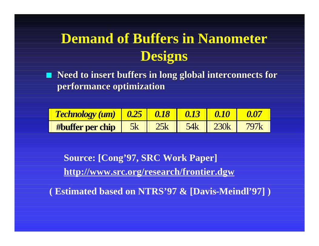
Demand of Buffers in Nanometer Designs
( Estimated based on NTRS’97 & [Davis-Meindl’97] )
Technology (um) 0.25 0.18 0.13 0.10 0.07 #buffer per chip 5k 25k 54k 230k 797k
nn Need to insert buffers in long global interconnects for Need to insert buffers in long global interconnects for performance optimizationperformance optimization
Source: [Cong’97, SRC Work Paper] http://www.src.org/research/frontier.dgw

ASPDAC'01 Tutorial Jason Cong 48
Buffer Block Planning Problem [Cong-Kong-Pan, ICCAD’99]
buffer block
nn Restriction from hard IP blocksRestriction from hard IP blocksnn Implications on P/G routingImplications on P/G routingnn Impact on Impact on floorplanfloorplan configurationconfiguration=> need to plan ahead for buffers.=> need to plan ahead for buffers.

ASPDAC'01 Tutorial Jason Cong 49
Optimal Buffer Location Can Be Relaxed
nn ClosedClosed--formform formula of feasible region (FR) for formula of feasible region (FR) for inserting one buffer to meet delay constraintinserting one buffer to meet delay constraint
1 bufferdriver
CLxmin l
xxmax
x M A XK K K K
K
x M I N l K K K KK
m i n
m a x
,
,
=− −
= + −
04
2
42
2 22
1 3
1
2 22
1 3
1
x x x∈[ , ]min max

ASPDAC'01 Tutorial Jason Cong 50
Feasible Region (FR) Is Very Large
nn Even under tight delay constraint, FR for BI can still Even under tight delay constraint, FR for BI can still be very large!be very large!
0
2000
4000
6000
8000
10000
0 0.1 0.2 0.3 0.4Delta
um
6000um 7000um 8000um 9000umv Delay budget is (1+Delta) Topt (the best delay by optimal buffer insertion)
Delta FR1% 19%5% 43%
10% 60%20% 86%
=> FR provides a lot of flexibility to plan buffer location

ASPDAC'01 Tutorial Jason Cong 51
Extension: 2D Feasible Region
nn FR extended to 2FR extended to 2--dimension with obstaclesdimension with obstacles
source
sink
2-D FR
Locus of min-delay BI (Restricted lines)
ASPDAC'01 Tutorial Jason Cong 52
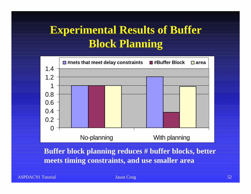
Experimental Results of Buffer Block Planning
Buffer block planning reduces # buffer blocks, better meets timing constraints, and use smaller area
00.20.40.60.8
11.21.4
No-planning With planning
#nets that meet delay constraints #Buffer Block area

ASPDAC'01 Tutorial Jason Cong 53
Concluding Remarks
nn HighHigh--performance designs in DSM technologies need performance designs in DSM technologies need carefully interconnect planningcarefully interconnect planning
nn Efficient interconnect performance estimation models Efficient interconnect performance estimation models ((IPEMsIPEMs) are important for interconnect planning) are important for interconnect planning
nn TopTop--level partitioning defines global and local level partitioning defines global and local interconnects, and impacts performance significantlyinterconnects, and impacts performance significantly
nn Retiming and pipelining over global interconnects are Retiming and pipelining over global interconnects are necessary for multinecessary for multi--gigahertz designsgigahertz designs
nn A clever combination of partitioning and retiming can A clever combination of partitioning and retiming can hide (some) global interconnect delayshide (some) global interconnect delays
nn Buffer block planning help to reduce complexity while Buffer block planning help to reduce complexity while achieving good performanceachieving good performance

ASPDAC'01 Tutorial Jason Cong 54
Acknowledgments
nn Thanks to Sung Lim, David Pan, and Thanks to Sung Lim, David Pan, and Xin Xin Yuan at Yuan at UCLA for their help with slidesUCLA for their help with slides
nn Thanks to SRC, MARCO/GSRC, and Intel Corp. for Thanks to SRC, MARCO/GSRC, and Intel Corp. for their supports of a number of research projects covered their supports of a number of research projects covered in this tutorialin this tutorial
nn Updated slides in PDF file will be available atUpdated slides in PDF file will be available athttp://http://cadlabcadlab..cscs..uclaucla..eduedu/~cong/~cong