neo gm650 hardware design manual version v1 · 2014-04-08 · neo_gm650 hardware design manual...
TRANSCRIPT

Neo_GM650
Hardware Design Manual
Version V1.2
Shenzhen Neoway Technology Co.,Ltd

Neo_GM650 Hardware design manual V1.2
All rights reserved by Shenzhen Neoway Technology Co., Ltd Page 2 Total 36
Copyright Statement
Copyright © 2008 Neoway Technology
All rights reserved by Shenzhen Neoway Technology Co.,Ltd.
The trademark belongs to Shenzhen Neoway Technology Co.,Ltd. Other trademarks,
mentioned in this manual, are property of to their lawful owners.
Clarification
This specification is aimed for use by system, research or test engineers.
With any future revisions of this product or due to other necessities, we may need to amend
the content of this specification without a prior notice.
Unless explicitly stated, all the information and suggestions in this manual do not carry any
implied guarantees.
Shenzhen Neoway Technology Co.,Ltd can provide the needed technical support. If you
experience problems, please feel free to contact the sales representative or send an E-mail
to any of the following mailboxes:
Website: www.neoway.com.cn

Neo_GM650 Hardware design manual V1.2
All rights reserved by Shenzhen Neoway Technology Co., Ltd Page 3 Total 36
Contents 1. Overview ....................................................................................................................... 5
2. Appearance .................................................................................................................. 5
3. Block Diagram ............................................................................................................. 6
4. Parameters ................................................................................................................... 6
5. Pin Definition & Encapsulation .................................................................................. 9
5.1 Pin Definition ............................................................................................................ 9
5.2 PCB Packaging....................................................................................................... 13
6. Design Reference ...................................................................................................... 14
6.1. Power supply & ON/OFF Interface ....................................................................... 14
6.1.1. Power Supply ........................................................................................................ 14
6.1.2. Power Sequencing ................................................................................................ 20
6.1.3. ON/OFF Pin Description ....................................................................................... 20
6.1.4. VCCIO Pin Description ......................................................................................... 23
6.1.5. RESET Pin Description ......................................................................................... 23
6.2. Serial Interface ....................................................................................................... 23
6.3. DTR and RING description .................................................................................... 26
6.3.1. DTR Pin Description ............................................................................................. 26
6.3.2. RING Signal Indication ......................................................................................... 27
6.4. SIM card interface .................................................................................................. 28
6.5. Indicator Light ........................................................................................................ 29
6.6. RF interface and PCB layout Design ................................................................... 29
6.6.1. RF connector of GPRS part .................................................................................. 29
6.6.2. RF part of GPS part .............................................................................................. 31
7. Assembly .................................................................................................................... 35
8. Packaging ................................................................................................................... 35
9. Abbreviations ............................................................................................................. 35

Neo_GM650 Hardware design manual V1.2
All rights reserved by Shenzhen Neoway Technology Co., Ltd Page 4 Total 36
Revision Record
Version Content Revised Effective date
V1.0 Initial version 2012-03
V1.1 Modify boot flag 2012-04
V1.2 Add UART2 pin and instructions, removed
the PWM pin, and added GPS data output
mode instructions.
2012-05

Neo_GM650 Hardware design manual V1.2
All rights reserved by Shenzhen Neoway Technology Co., Ltd Page 5 Total 36
1. Overview
GM650 is an open platform wireless industrial module, supporting GSM/GPRS+GPS. It
provides the user with reserved CPU resource and plenty of hardware interfaces, widely
used in various industrial and commercial applications. The module has high quality voice,
messaging, data connectivity, GPS location and other functions.
GM650 allows two configurations for the GPS data interface: single-port and dual-port.
The single port configuration is a perfect solution in cases where the user’s MCU has only
one available UART interface to support both the GPRS communication and GPS
positioning functions.
2. Appearance
Table 2-1 GM650 Mechanical Specifications
Specifications Description
Dimensions 30.0mm*24.0mm*2.7mm (length*width*height)
Weight 3.7g
Picture

Neo_GM650 Hardware design manual V1.2
All rights reserved by Shenzhen Neoway Technology Co., Ltd Page 6 Total 36
3. Block Diagram
4. Parameters
Table 4-1
General parameters Description
Operating temperature -30℃~+70℃
Operating voltage 3.5V~4.3V (recommended 3.9V)
Operating Current See tables 4-2 and 4-3
Table 4-2
GSM Specifications Description
Frequency 900/1800/850/1900 MHz
Sensitivity < -106dBm
Maximum transmission
power
850/900 Class4 (2W)
1800/1900 Class1 (1W)
Protocol Compatible with GSM/GPRS Phase2/2+
AT GSM07.07
Extended command set
Audio FR、EFR、HR、AMR voice coding
GSM
Baseband
Controller
PA
Power
Manager
Ap
plicatio
n In
terface RF
Section
GPS Section
Audio
Section
SIM x 2
UART x 2
I2C
MMC
USB
ADC/PWM
LCD
Flash

Neo_GM650 Hardware design manual V1.2
All rights reserved by Shenzhen Neoway Technology Co., Ltd Page 7 Total 36
SMS TEXT/PDU
Point to point/cell broadcast
Grouped Data GPRS CLASS 12
Circuit Switched Data Support CSD data service
Support USSD
Supplement Service Call forward(CFB,CFNA,CFU)
Call waiting
Threeway calling
Main Processor ARM7-EJ@104MHz, 32Mbits SRAM, 32~64Mbits NOR
Flash
Reserved software
resource
16Mbits RAM,16~32Mbits Flash
Reserved software
resource
UART x 2,I2C,LCD(SPI),MMC,USB,ADC,PWM,
GPIO x 20,Keypad
Instantaneous Current Max 1.8A
Average working Current < 300mA
Standby Current 2.5mA typ.
Table 4-3
GPS Specifications Description
GPS C/A coding 1.023 MHz chip rate
GPS Channel 48 channels tracking
GPS Sensitivity -162dBm
Position Accuracy 10m
Speed Accuracy 0.01 m/s
Time Accuracy Synchro with GPS Satellite time(<60ns)
Time of hot start <1s
Time of warm start <35s
Time of cold start <35s
Time of recapture <0.1s
GPS data updating
frequency
2Hz

Neo_GM650 Hardware design manual V1.2
All rights reserved by Shenzhen Neoway Technology Co., Ltd Page 8 Total 36
Height limit 18288m
Speed limit 515 m/s or 1854Km/h
Acceleration limit <4g
Average working current
(tracking mode)
< 38mA
Average working current
(getting posotion)
< 45mA
Note: The starting time, working current and other GPS parameters relate to the testing
environment, including whether is under open sky, thickness of the clouds and so on.

Neo_GM650 Hardware design manual V1.2
All rights reserved by Shenzhen Neoway Technology Co., Ltd Page 9 Total 36
5. Pin Definition & Encapsulation
5.1 Pin Definition
The signal connection uses 74 SMD pads of stamp-hole type (half hole).
Note: GM650 module IO interface level is 2.8V.
The module’s internal IO uses 2.8V power supply system, which sets the input voltage for
all IO pins must not exceed the maximum of 3.3V, otherwise it may damage the module’s
IO. Possible signal integrity problems in circuits using 3.3V power may lead to overshooting
and output voltages surpassing the 3.3V limit and rising as high as 3.5V sometimes. Such
situation will cause damage to the IO port if a 3.3V signal is directly connected to the 2.8V
module IO. Hence a level matching external circuit should be used to properly interface with
the IO port. Please refer to chapter 6.2 for more details.
Table 5-1 GM650 Pin Definition
Pin Signal Name I/O Function Description Remark
1 GND PWR Ground
2 Reserved Reserved
3 Reserved Reserved
4 URXD1 DI UART1 data receive
input
Used for GPRS communication
and AT commands
5 UTXD1 DO UART1 data transmit
output

Neo_GM650 Hardware design manual V1.2
All rights reserved by Shenzhen Neoway Technology Co., Ltd Page 10 Total 36
6 NC Reserved Must be left floating
7 UTXD2 DO UART2 data transmit
output; baud rate
= 9600
In dual-port mode carries the GPS
data;
Unused in single-port mode
8 Reserved DO PWM output Must externally connect a 100k
pull-down resistor
9 GND PWR Ground
10 Reserved Reserved
11 Reserved Reserved
12 VCCIO AO 2.8V output Can be power supply for the IO
level shifting circuit;
Load capacity <50mA
13 VRTC PWR RTC power 2.8V,the highest output current is
2mA
14 BACK_LIGHT DO working station indicator,
output square signal of
0.5s high level, 1.5s low
level
High level light LED; needs a
capacitor of 0.1uF connected in
parallel
15 Reserved Reserved
16 Reserved Reserved
17 RESET DI Reset Soft reset input, low level reset
18 Reserved Reserved
19 Reserved Reserved
20 GND PWR Ground
21 ANT_GSM I/O GSM antenna RF
interface
22 GND PWR Ground
23 DTR DI Low power consumption
set
Refer to chapter 6.3
24 Reserved Reserved
25 Reserved Reserved
26 Reserved Reserved
27 KCOL0 DI Keyboard column scan 0 While using the serial interface to
update software version, pin27
KCOL0 must be set at high level
28 ON/OFF DI ON/OFF input Low level pulse changes the
ON/OFF state;
Keep in high level;
Refer to chapter 6.1.3
29 Reserved Reserved
30 Reserved Reserved
31 Reserved Reserved

Neo_GM650 Hardware design manual V1.2
All rights reserved by Shenzhen Neoway Technology Co., Ltd Page 11 Total 36
32 RING DO Ring output Refer to chapter 6.3
33 Reserved Reserved
34 Reserved Reserved
35 Reserved Reserved
36 Reserved Reserved
37 GND PWR Ground
38,39 VBAT PWR Main Power 3.5V~4.3V,recommended 3.9V
40 Reserved Reserved
41 Reserved Reserved
42 Reserved Reserved
43 Reserved Reserved
44 GND PWR Ground
45 Reserved Reserved
46 Reserved Reserved
47 Reserved Reserved
48 Reserved Reserved
49 VSIM1 PWR Power of SIM card 1 Compatible with 1.8/3.0V SIM
cards
50 SIM1_CLK DO Clock of SIM card 1
51 SIM1_RST DO SIM card 1 reset
52 SIM1_DATA DIO Data input/output of SIM
card 1
Built-in 5k pull-up resistor
53 GND PWR Ground
54 MICP AI Positive electrode of
MIC audio input
Alternating peak voltage ≤200mV
55 MICN AI Negative electrode of
MIC audio input
Alternating peak voltage ≤200mV
56 EARN AO Positive electrode of
earphone audio output
32Ω earphone driving output
57 EARP AO Negative electrode of
earphone audio output
32Ω earphone driving output
58 SPKN0 AO Negative electrode of
speaker output
Maximum 0.9W@8Ω
59 SPKP0 AO Positive electrode of
speaker output
Maximum 0.9W@8Ω
60 Reserved Reserved Built-in internal 100k pull-up
resistor
61 Reserved Reserved
62 Reserved Reserved
63 Reserved Reserved
64 Reserved Reserved
65 GND PWR Ground

Neo_GM650 Hardware design manual V1.2
All rights reserved by Shenzhen Neoway Technology Co., Ltd Page 12 Total 36
66 Reserved Reserved
67 Reserved Reserved
68 Reserved Reserved
69 Reserved Reserved
70 CLK32K DO 32.768kHz real-time
clock output
71 Reserved Reserved
72 Reserved Reserved
73 GND PWR Ground
74 ANT_GPS I/O GPS antenna RF
interface

Neo_GM650 Hardware design manual V1.2
All rights reserved by Shenzhen Neoway Technology Co., Ltd Page 13 Total 36
5.2 PCB Packaging
The signal connections use 74 SMD pads of stamp-hole type (half hole) and pitch of
1.27mm. The PCB encapsulation we recommend is as in figure 5-1. Dimensions in
millimeters.
Figure 5-1 Recommended PCB footprint(top view)
Note:The number in the brackets stands for coordinate position of the pad. Origin point is
the center of the module.
The number below the coordinate stands for shape size of the pad’s LxW.
The top right corner and the bottom right corner are two circle regions (R=1.3). The circle
regions are route keep out regions. For the routing requirements refer to chapter 6.6.

Neo_GM650 Hardware design manual V1.2
All rights reserved by Shenzhen Neoway Technology Co., Ltd Page 14 Total 36
6. Design Reference
6.1. Power supply & ON/OFF Interface
Table 6-1 Power supply & ON/OFF Interface
Pin Signal
Name I/O Function Description Remark
12 VCCIO PWR 2.8V power output Can be power supply for
the IO level shifting
circuit;
Load capacity <50mA
13 VRTC PWR RTC power input 2.8V
17 RESET DI Reset input Soft reset input, low level
reset
28 ON/OFF DI ON/OFF input,low level pulse
changes the ON/OFF state
38-39 VBAT PWR Main power supply input 3.5V~4.3V
6.1.1. Power Supply
VBAT is the main power supply of the module, with power input in the range of 3.5V~4.3V.
The recommended operating voltage is 3.9V. VBAT supplies power to all digital signal and
analog signal sub-systems in the module as well as to the RFPA.
The performance of VBAT will directly affect the performance and stability of the whole
module. The average power consumption of the module is below 1.2W, but the maximum
instantaneous current on the VBAT pin is 1.8A. In the power circuit, it is needed to add a
high capacity aluminum electrolytic capacitor or a lower capacity tantalum
electrolytic capacitor to strengthen the instant large current free-wheeling ability of the
power. The higher the capacity is, the lower maximum current of the power output needs to
be.

Neo_GM650 Hardware design manual V1.2
All rights reserved by Shenzhen Neoway Technology Co., Ltd Page 15 Total 36
It is also needed to add filter capacitors of 0.1uF, 100pF and 33pF to reduce the influence of
the radio frequency interference. Add a capacitor of low impedance and high capacity near
to the module. The detailed testing data is as the following picture:
Figure 6-1
The data above is related to the equivalent impedance of the capacity and the internal
resistance of the power. For C1 we recommend to use a 1000uF aluminum electrolytic
capacitor of low impedance. A 470uF tantalum electrolytic capacitor can be used instead, if
the space is limited. If the power is supplied by lithium battery directly, C1 could be a 220uF
or 100uF tantalum capacitor.
Maximum current is drawn during calls with weak signal or data transmission process.
Typical current and voltage curve is as below:

Neo_GM650 Hardware design manual V1.2
All rights reserved by Shenzhen Neoway Technology Co., Ltd Page 16 Total 36
Figure 6-2
The power design of VBAT should ensure that the instantaneous current can’t be lower than
3.5V, otherwise the module will not work properly. The main power supply can’t exceed 4.3V,
otherwise will cause damage because of overvoltage. The recommended voltage for VBAT
is 3.9V.
In remote applications or conditions with high electromagnetic interference, it must be
ensured that the power is ON/OFF controlled. Use the EN pin of LDO or DC-DC to control
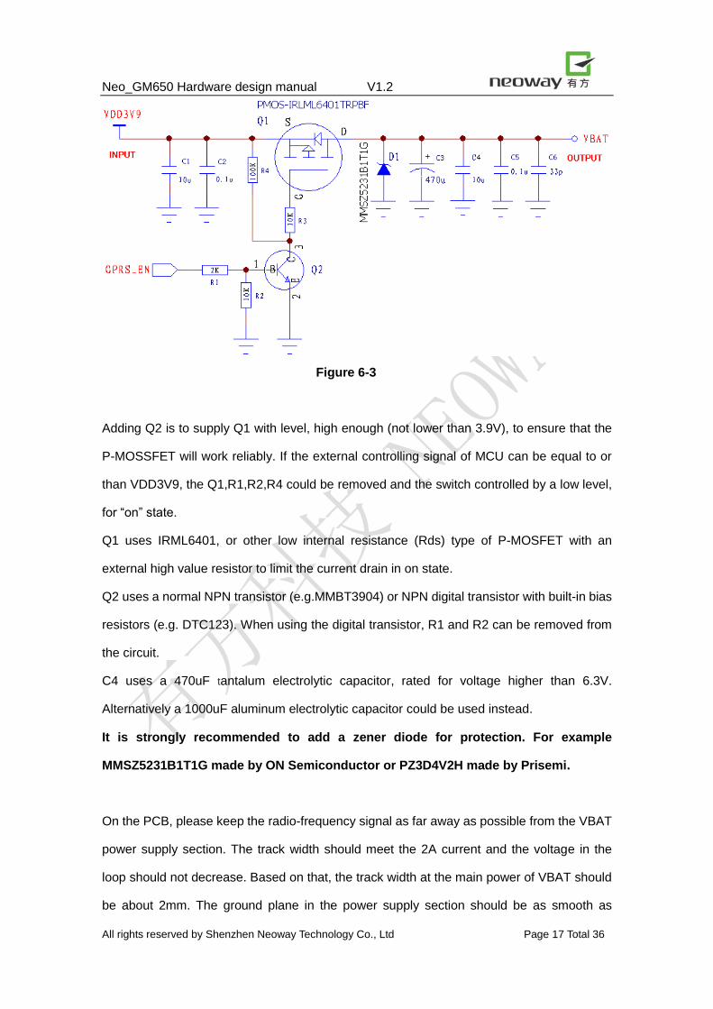
the power ON or OFF. If there is no controlling switch in the power system, please refer to
figure 6-3 for a P-MOSFET electronic switch. According to it, when GPRS_EN is high level,
the switch will be on.
Neo_GM650 Hardware design manual V1.2
All rights reserved by Shenzhen Neoway Technology Co., Ltd Page 17 Total 36
Figure 6-3
Adding Q2 is to supply Q1 with level, high enough (not lower than 3.9V), to ensure that the
P-MOSSFET will work reliably. If the external controlling signal of MCU can be equal to or
than VDD3V9, the Q1,R1,R2,R4 could be removed and the switch controlled by a low level,
for “on” state.
Q1 uses IRML6401, or other low internal resistance (Rds) type of P-MOSFET with an
external high value resistor to limit the current drain in on state.
Q2 uses a normal NPN transistor (e.g.MMBT3904) or NPN digital transistor with built-in bias
resistors (e.g. DTC123). When using the digital transistor, R1 and R2 can be removed from
the circuit.
C4 uses a 470uF tantalum electrolytic capacitor, rated for voltage higher than 6.3V.
Alternatively a 1000uF aluminum electrolytic capacitor could be used instead.
It is strongly recommended to add a zener diode for protection. For example
MMSZ5231B1T1G made by ON Semiconductor or PZ3D4V2H made by Prisemi.
On the PCB, please keep the radio-frequency signal as far away as possible from the VBAT
power supply section. The track width should meet the 2A current and the voltage in the
loop should not decrease. Based on that, the track width at the main power of VBAT should
be about 2mm. The ground plane in the power supply section should be as smooth as

Neo_GM650 Hardware design manual V1.2
All rights reserved by Shenzhen Neoway Technology Co., Ltd Page 18 Total 36
possible, and ground holes are recommended.
If problems arise under low temperature conditions, the highest failure rate will probably be
in the power supply section. The power supply ripple increases with the decrease of load
capacitance. Under low temperature conditions, the activity in the electrolytic capacitors will
lead to decrease in their capacitance, ESR will increase, and that will weaken the filtering
effect. It is recommended to use electrolytic capacitors which have good performance under
low temperature conditions or under high pressure conditions or enlarge the total
capacitance. A proper capacitor with its capacity and impedance should be carefully
selected. So please be careful when you design the product to work under low temperature
conditions especially considering the power supply section.
Prohibit the use of power from the diodes’ voltage drop directly since it will enlarge the
diode’s voltage drop tremendously under the low temperature conditions, and that will lead
to great power supply fluctuations which can make the module unstable.
When you are testing the static electricity and surge, please ensure the stability of the power
supply. Some EMC design may be considered to add to the input and output interfaces in
order to avoid the burr and peak. It is recommended to properly increase the filtering
capacitors to ensure the power supply stability. For example, some 1~4.7uF ceramic
capacitors could be added in parallel.
VRTC is power supply pin of the real-time clock (RTC). When the VBAT supply works
well, VRTC will continuously output 2.8V voltage. The modules can apply to charge button
batteries or a bulk capacitor. The current is 2mA. When the VBAT is off-power, the button
batteries or bulk capacitor can power the RTC to keep the RTC clock work properly. The
capacity of energy storage capacitor should be as large as possible. If the 100uF tantalum
electrolytic capacitors are used in the system, it can keep the clock working for 1 minute
after the shutting off the VBAT.

Neo_GM650 Hardware design manual V1.2
All rights reserved by Shenzhen Neoway Technology Co., Ltd Page 19 Total 36
Please refer to figure 6-4:
Figure 6-4
VRTC can also be designed in a way as in figure 6-5:
Figure 6-5
If the module ran into a problem in a low temperature of -40°, the problem will be most
probably caused by the power supply, and will expressed in the increase of the power
supply ripples and the decrease of the load capacitance. If the lowest point in the ripples is
lower than or close to 3.3V, the module will automatically shut down to for protection. In
addition, if the power is supplied from a DC/DC converter, the performance of IC and any
inductors will vary significantly under temperatures of around -40°. Therefore, when
designed for ultra-low temperature applications, the power supply circuit requires caution.

Neo_GM650 Hardware design manual V1.2
All rights reserved by Shenzhen Neoway Technology Co., Ltd Page 20 Total 36
It is forbidden to supply the power by diode direct buck. That may cause unstable operation
of the module.
6.1.2. Power Sequencing
Figure 6-6 Power Sequencing
Note: Module’s main power supply shouldn’t be powered on earlier than the external MCU.
Please ensure that the module is powered on after the MCU in order to guarantee its stable
work.
6.1.3. ON/OFF Pin Description
The ON/OFF pin is an input, controlled by external signal. The input has active low level.

Neo_GM650 Hardware design manual V1.2
All rights reserved by Shenzhen Neoway Technology Co., Ltd Page 21 Total 36
Power on process: When the module is in the shutdown mode, first pull the ON/OFF base
pin down to low level and maintain for more than 300ms (recommended for at least 500ms),
then pull the ON/OFF base pin up to a high level, to start the module. (figure 6-6).
When the module is powered on, the module's serial port will automatically output "+ EIND:
1", said the module has started successfully and is now controllable by AT commands. The
VCCIO will start to continuously output 2.8V.
Power off process: Under the start-up mode, if the ON/OFF is high level, this time pull low
the ON/OFF pin and maintain for 300ms (recommended for at least 500ms), then the
module will enter the shutdown process to disconnect from the network, it usually takes
about 5 seconds for the module to completely shut down and then the main power turned off;
If the ON/OFF is low level, pull the ON/OFF up for some time before the execution of the
shutdown sequence described above. An AT command can also be used to shut the module
down; please refer to the AT command manual.
If you want to change the switch electrical and mechanical level, an inverter should be used.
Figure 6-7 shows the recommended GM650 power on/off circuit with high level active input:
Figure 6-7 Recommended high level power on circuit

Neo_GM650 Hardware design manual V1.2
All rights reserved by Shenzhen Neoway Technology Co., Ltd Page 22 Total 36
The GM650 ON/OFF is low level effective. After the level inversion above, the USER_ON is
high level on. The ON/OFF pin can also be connected to GND for simplicity. The module will
automatically be on after power on in that case.
A proper control of the ON/OFF pin by the user’s software must be ensured in order to
guarantee the module’s operation.
Note: ON/OFF base pin has the function of start-up and shut-down, thus be careful to avoid
repeated triggering which will result in confusion of start-up or shut-down. For example, if
the user wants to start up, but a 300ms high pulse is issued twice to the ON/OFF pin, the
module will shut down immediately after start up.
Furthermore, pay attention to external MCU and module connection interface level,
especially UART, which may affect the module boot timing. For example, when starting up,
the external MCU has an IO port in output state while the same port is the module’s UART
port UTXD signal (which is also an output pin), the module may be unable to start up.
Also note that, if the module has voltage on some input before starting up, it may also affect
the boot timing. If you provide the module VBAT supply and then use the ON/OFF signal, it
may cause a start-up failure. Therefore, in order to guarantee reliable start-up process, it is
recommended that the ON/OFF should be in low level first, and then give the module VBAT
supply. Then after the module has started completely, pull the ON/OFF control pin back to a
high level.
The ON/OFF controls the module’s internal software. If the module has not started properly,
it may be unable to respond to the ON/OFF pin anymore and a forced VBAT power
disconnection should be used in such case.

Neo_GM650 Hardware design manual V1.2
All rights reserved by Shenzhen Neoway Technology Co., Ltd Page 23 Total 36
6.1.4. VCCIO Pin Description
Pin 12 VCCIO is the 2.8V IO interface voltage, which the module supplies to an external
circuit. It has a load capacity of 50mA and is suggested to be used for level shifting interface
only. In power off state then VCCIO output also off.
Moreover, this pin can be used to indicate the running state of the module. When running
normal or in sleep mode, the pin is kept at high level 2.8V, while in power off modem, the pin
is low level.
6.1.5. RESET Pin Description
Pin 17 of GM650 is RESET input pin. The module will reset on low lever on this pin.
This pin controls the module’s internal software and in case of a software crash due to
improper operation, it may not be able to trigger reset.
6.2. Serial Interface
Table 6-2 Serial interface
PIN Signal
Name
I/O Function Description Remark
4 URXD1 DI UART1 data receiving
5 UTXD1 DO UART1 data transmitting
7 UTXD2 DO UART2 data transmitting,
baud rate= 9600
Dual-port mode: used to receive
GPS data;
Single-port mode: unused.
The serial interface is usually used for AT commands, data services, module firmware
updates and so on.
The module is a DCE device. The connection signals with a terminal device (DTE) are
shown in the following picture:

Neo_GM650 Hardware design manual V1.2
All rights reserved by Shenzhen Neoway Technology Co., Ltd Page 24 Total 36
Figure 6-8 Connection between DCE and DTE
The serial interface of GM650 is 2.8V CMOS; the maximum input level is 3.3V.
Supported baud rates are:
UART1: 1200,2400,4800,9600,19200,38400,57600,115200; default is 115200bps.
UART2: 9600. In dual-port mode used to output GPS data. In single-port mode UART2 is
unused.
If the main power supply for the external MCU is 3.3V, a 200~330ohm resistor is
recommended in series to the module. In the PCB layout, this resistor should be placed
close to the output of the signal source, while the capacitor should be placed close to the
module on the receiving end. Refer to the following figure:
Figure 6-9 3.3V MCU communication via serial interface
A 100pF or 200pF filter capacitor should be placed close to the module receiver pin. The
values of the resistors and capacitors can be selected based upon the measured signal

Neo_GM650 Hardware design manual V1.2
All rights reserved by Shenzhen Neoway Technology Co., Ltd Page 25 Total 36
waveform. Greater the resistance and capacitance values will provide higher attenuation,
but also will lead to greater signal delay or signal waveform distortions and lower baud rates
on the serial communication, Therefore, the resistance and capacitance should be carefully
selected.
When the user’s external MCU voltage is 5V, the serial interface needs to be level-shifting
as in the reference circuit below:
Ficure 6-10 5V MCU communication via serial interface
“INPUT” connects to the external MCU’s TXD, “VCC_IN” is the external MCU’s 5V power
supply, “OUTPUT” connects to the GM650‘s RXD input, and “VCC_OUT” is provided by the
module’s VCCIO (2.8V) output.
Another copy of the level-shifting circuit must be used in the second communication wire.
The R3 is a 4.7K~47K resistor and R2 is a 3.3K~10K resistor. Resistance selection is
related to the supply voltage and the serial port baud rate. When the supply voltage is higher
or the baud rate is lower, the resistors can be of higher resistance which will lead to lower
power consumption.
Q1 may be an ordinary NPN transistor (for example, MMBT3904) or built-in bias resistors
NPN digital transistor (for example DTC123). When using the digital transistor, R2 can be
removed from the circuit.

Neo_GM650 Hardware design manual V1.2
All rights reserved by Shenzhen Neoway Technology Co., Ltd Page 26 Total 36
Note: Avoid serial data generated when the module is powering up. Data to the module
should only be sent after the completion of the module’s start-up procedure (at least 2s).
The purpose is to avoid forcing the module into a wrong mode of operation.
Take care to avoid crosstalk between the TXD and RXD lines by keeping them apart with
spacing at least 3 times the track width. Avoid running the lines in parallel to each other for
long distances, and where possible run a ground plane close to these lines to avoid
interference. Use through holes to link the ground planes on the various layers.
6.3. DTR and RING description
Table 6-3
PIN Signal
Name
I/O Function Description Remark
32 RING DO Ring output
23 DTR DI Low power consumption mode
controlling input
6.3.1. DTR Pin Description
DTR is the low power control pin, and if not required can remain unconnected. For
low-power usage, please see the AT commands. Using AT command to enable the low
power capabilities, set DTR pin to low, if the module is idle, then enter low-power mode. In
low power mode, the standby current is approximately 2.5mA.
In low power mode, the module will timely respond the call, SMS and data services. External
MCU can control module hardware IO (DTR pin) to exit the sleep mode.
Basic process for entering the sleep mode:
1) Keep the module DTR input high while issuing the AT command to allow entering sleep
mode (refer to the AT command AT+ENPWRSAVE). In this mode, the run light stops
flashing.
2) Pull the DTR input low. Typically the module will enter sleep mode in about 2 seconds.
In sleep mode, the serial port of the module is disabled and will not respond to data. The

Neo_GM650 Hardware design manual V1.2
All rights reserved by Shenzhen Neoway Technology Co., Ltd Page 27 Total 36
module will only enter into sleep mode, if there is no data present on the serial port,
otherwise the module will wait until the completion of the current data transfer to end before
entering sleep mode.
3) If the serial port has data the MCU can place DTR high. The module will immediately
exit sleep mode and within 50ms will be back to normal operation mode, and the serial port
will respond to AT commands. After the completion of the calling service, the external MCU
may pull DTR low and place the module into sleep mode again.
4) In sleep mode, if the module received calls, messages or data from the server, it will
immediately exit sleep mode and output call information through the serial port. After the
external MCU has detected activity on the serial port, the DTR line should be set high, to
process calls, data etc. When processing is complete, the module will go into sleep mode
upon DTR being set low. If there is a call, and DTR is not set high, no data will be
transmitted over the serial port and the module will automatically enter into sleep mode in
approximately 2 seconds.
6.3.2. RING Signal Indication
1) Voice calls:
For incoming voice calls, the UART port will transmit a "RING" string while the RING pin will
cycle in 4s pulses with the line kept in low level for 250ms during each cycle for the whole
ringing time. It will revert back to constant high level after the call is connected. Please refer
to the figure below:
Figure 6-11 Voice calls RING indication

Neo_GM650 Hardware design manual V1.2
All rights reserved by Shenzhen Neoway Technology Co., Ltd Page 28 Total 36
2) SMS:
Incoming SMS will be indicated with a single 200ms pulse.
Figure 6-12 SMS indication
6.4. SIM card interface
Table 6-4 SIM card interface
Pin Signal Name I/O Function Description remark
49 VSIM1 PWR SIM card1 power supply 1.8/3.0V
50 SIM1_CLK DO SIM card 1 clock
51 SIM1_RST DO SIM card1 reset
52 SIM1_DATA DIO SIM card1 data
input/output
Ficure 6-13 SIM card interface design
GM650 module supports 3V and 1.8V SIM cards.
VSIM is the power supply pin for SIM card with load capacity up to 30mA. This power output
only operates when the module works with the SIM card.
The SIM_DATA line has an internal 5k pull-up resistor and does not require any externally

Neo_GM650 Hardware design manual V1.2
All rights reserved by Shenzhen Neoway Technology Co., Ltd Page 29 Total 36
connected pull-up resistors.
The SIMCLK line is the SIM card clock, normally 3.25MHz. The PCB clock distribution track
must be kept smooth and in one piece. It has to be as short as possible, surrounded with
ground and kept away from the antenna and other RF components. The capacitance
(containing the junction capacitance of the ESD device) of this signal cannot be over 100pF.
It is recommended to have the SIM card circuit close to the card connector. Except for the
VSIM pin, which uses a 0.1uF capacitor, the other SIM card pins shall have 27~33pF
capacitors to ground (refer to figure 6-11). This capacitance shall be put as close as possible
to the relevant pin of the SIM card.
Note:Small filter capacitance is mainly to prevent any interference from the antenna when it
is too close to the module and the SIM card and otherwise may result the card will not be
read normally or the antenna’s reception sensitivity got worse, especially when using a short
rubber antenna or internal antenna.
6.5. Indicator Light
Table 6-5 Indicator light
Pin Signal Name I/O Function Description remark
14 BACK_LIGHT O Working state indicator
When the module is operating, the indicator light will be on for 0.5s and off for 1.5s.
Note: Connect a 0.1uF capacitor in parallel with the BACK_LIGHT pin.
6.6. RF interface and PCB layout Design
The GPRS RF and GPS RF sections should be as far away from each other as possible,
including all participating tracks in the PCB layout and the antennas.
6.6.1. RF connector of GPRS part
Pin 21 is GSM RF interface with impedance of 50Ω and can be connected to a ZYJB, sucker
antenna, built-in PIFA antenna or other type antenna. The RF track should conform to the
necessary rules in order to avoid signal interference.

Neo_GM650 Hardware design manual V1.2
All rights reserved by Shenzhen Neoway Technology Co., Ltd Page 30 Total 36
The antenna used should have a standing-wave ratio of 1.1~1.5 and input impedance of
50Ω. The requirements towards the antenna vary with the environment. In general, higher
the intra-band gain results lower out band gain and a better performance of the antenna.
When using multi ports antenna, the isolation between each port should be more than 30dB.
If there is a RF PCB track between the module and the antenna, it must be 50Ω impedance
controlled and the length should be as short as possible.
If a longer antenna track is needed, please add a π-matching network as in the picture
below.
Ficure 6-14
In two layer boards the RF track should be as short as possible. The suggested parameters
ate: width of 0.8~1.0mm, and the space between RF and the ground about 1~0.8mm. The
RF track should be short and smooth. Please refer to figure 6-15, which demonstrates a two
layer board application. The RF signal connects to GSC RF connector via PCB track, and
the antenna is connected to the board via cable.
There shouldn’t be any tracks right under the GPRS module.

Neo_GM650 Hardware design manual V1.2
All rights reserved by Shenzhen Neoway Technology Co., Ltd Page 31 Total 36
RF testing point is at PCB projection area. It is needed to have a copper dug area with a
diameter of 1.4mm. There shouldn’t be any track in this area. There should be isolation
between this area and the copper dug area of pin 57 and shouldn’t be any track or copper in
the top layer, the second layer needs to be a copper area. The other PCB layers can
contain tracks.
Figure 6-15
Note: The RF signal and RF components in the user's system should be located away from
the high-speed circuits, switching power supplies, power transformers, large inductance
and single-chip clock circuits.
6.6.2. RF part of GPS part
Pin 74 is RF GPS interface, PCB layout impedance requirement is for 50Ω with the RF track
as short as possible. Users can refer to the GSM section for more details. The requirements
towards the GPS routing are even tougher because the GPS air wireless signal strength is
RF wiring width of 0.8~1mm, length as
short as possible, clearance to the
ground of 0.8~1mm, wiring around
need to dig full ground holes.
Pins 20 and 22 need to
connect to ground on
both sides completely,
no half-connect ground
conditions.
Module RF test point
below the surface needs
to dig copper, about
1.5mm in diameter and
should be surrounded by
paved ground.
Module RF test point to
dig copper area should
be isolated by ground
against RF wiring to dig
copper area.

Neo_GM650 Hardware design manual V1.2
All rights reserved by Shenzhen Neoway Technology Co., Ltd Page 32 Total 36
lower which results in weaker electrical signal which the antenna receives. Weaker signals
are more susceptible to interference.
A ceramic GPS chip antenna can be used. It is suggested to use an active antenna. From
the antenna the GPS satellite signal, passes through the active antenna front-end LNA (low
noise amplifier) to be amplified, then goes through the connector and a PCB layout track
fed into GM650’s pin 74. The connector and the PCB tracks, require 50Ω impedance control,
and tracks to be as short and smooth as possible.
For users with advanced RF design skills and doing multilayer PCB, a passive ceramic or
other type of GPS antenna design can be implemented with a proper routing and thorough
testing. Passive GPS antennas may reduce the BOM cost, but require better understanding
the matter in order to produce a reliably working board.
Figure 6-16
The figure below is a practical implementation of an LNA circuit design for GM650, which
has been used in a product and possesses excellent performance.

Neo_GM650 Hardware design manual V1.2
All rights reserved by Shenzhen Neoway Technology Co., Ltd Page 33 Total 36
Figure 6-17
If the antenna and the PCB layout are not properly designed, the sensitivity of the GPS will
decrease leading to low positioning accuracy or long signal acquisition times.
Re-emphasis, GPRS and GPS RF sections, including the PCB layout tracks and antenna,
must be placed as far away as possible to prevent these two parts from interfering with
each other.
6.7. GPS data interface mode instructions
GPS data can be fed into the user’s application by using one of the two possible modes for
the serial interface.
6.7.1. Single-port mode
GPS data is sent to the GPRS baseband chip and available via AT commands to the user’s
MCU via CM650’s UART1. The user has indirect access to the GPS data. For the related

Neo_GM650 Hardware design manual V1.2
All rights reserved by Shenzhen Neoway Technology Co., Ltd Page 34 Total 36
AT-command please see GM650 module AT command set. GM650 has only one UART
interface for the user which is suitable for MCUs that have only one available UART port to
support both GPRS communications and GPS positioning.
Figure 6-18
6.7.2. Dual-port mode
In dual-port mode, GM650 provides two independent UART interfaces: UART1 for GPRS
communications and AT commands and UART2 for GPS data. UART2 outputs GPS data in
NMEA-compliant format with baud rate 9600bps.
Figure 6-19
Dual-port model, GM650 provides two independent UART interfaces.
UTXD1
URXD1

Neo_GM650 Hardware design manual V1.2
All rights reserved by Shenzhen Neoway Technology Co., Ltd Page 35 Total 36
6.8. Module hardware design considerations
When using the serial port to download, the pin 27 KCOL0 must be kept at high level,
otherwise the download cannot be initiated.
7. Assembly
The GM650 module uses 74 SMD pads of stamp-hole type (half hole).
8. Packaging
In order to prevent the product of from being affected with damp, caused by using the SMT
way to perform the furnace welding, in the process of production and use of the costumer,
we employ the way of damp-proof packing, such as Aluminum Foil Bag, desiccating agent,
Humidity Indicator Cards, Suck plastic trays, and vacuolization. As a result the product is
kept dry and its life span will be long.
In order to make the SMT way easy, we use the tray to load the product. The user only
needs to install it in the chip mounter according to the fixed direction.
For GM650 storage and SMT notes please refer to <Neoway module SMT reflow production
recommendation_V1.0>.
9. Abbreviations
ADC Analog-Digital Converter 模数转换
AFC Automatic Frequency Control 自动频率控制
AGC Automatic Gain Control 自动增益控制
AMR Acknowledged multirate (speech coder) 自适应多速率
CSD Circuit Switched Data 电路交换数据
CPU Central Processing Unit 中央处理单元
DAI Digital Audio interface 数字音频接口
DAC Digital-to-Analog Converter 数模转换
DCE Data Communication Equipment 数据通讯设备
DSP Digital Signal Processor 数字信号处理
DTE Data Terminal Equipment 数据终端设备
DTMF Dual Tone Multi-Frequency 双音多频

Neo_GM650 Hardware design manual V1.2
All rights reserved by Shenzhen Neoway Technology Co., Ltd Page 36 Total 36
DTR Data Terminal Ready 数据终端准备好
EFR Enhanced Full Rate 增强型全速率
EGSM Enhanced GSM 增强型 GSM
EMC Electromagnetic Compatibility 电磁兼容
EMI Electro Magnetic Interference 电磁干扰
ESD Electronic Static Discharge 静电放电
ETS European Telecommunication Standard 欧洲通信标准
FDMA Frequency Division Multiple Access 频分多址
FR Full Rate 全速率
GPRS General Packet Radio Service 通用分组无线业务
GSM Global Standard for Mobile Communications 全球移动通讯系统
HR Half Rate 半速率
IC Integrated Circuit 集成电路
IMEI International Mobile Equipment Identity 国际移动设备标识
LCD Liquid Crystal Display 液晶显示器
LED Light Emitting Diode 发光二极管
MS Mobile Station 移动台
PCB Printed Circuit Board 印刷电路板
PCS Personal Communication System 个人通讯系统
RAM Random Access Memory 随机访问存储器
RF Radio Frequency 无线频率
ROM Read-only Memory 只读存储器
RMS Root Mean Square 均方根
RTC Real Time Clock 实时时钟
SIM Subscriber Identification Module 用户识别卡
SMS Short Message Service 短消息服务
SRAM Static Random Access Memory 静态随机访问存储器
TA Terminal adapter 终端适配器
TDMA Time Division Multiple Access 时分多址
UART Universal asynchronous receiver-transmitter 通用异步接收/发送器
VSWR Voltage Standing Wave Ratio 电压驻波比