national vacuum electronics conference nvec 2019
TRANSCRIPT

National Vacuum Electronics Conference
NVEC 2019
Programme and Book of Abstracts
Technology and Innovation Centre,
University of Strathclyde,
Glasgow, G1 1RD, UK
Wednesday 13 November 2019
Sponsor
SUPA, Department of Physics,
University of Strathclyde
Organisers:
Dr. Liang Zhang, Professor Adrian W. Cross


Conference Schedule
Wednesday 13 November 2019
8:30 – 9:15 Arrival, registration
9:15 – 9:20 Announcements
Prof. Adrian Cross
9:20 – 11:00 Session I Microwave Vacuum Electronic Devices
Chair: Dr. Craig Donaldson
9:20 – 9:40
(1)
Tianzhong Zhang
School of Electronic Engineering and Computer Science, Queen Mary
University of London
“Design of a high power W-band rising-sun anode magnetron”
9:40 – 10:00
(2)
Laurence Nix
SUPA, Department of Physics, University of Strathclyde, Glasgow, G4 0NG, UK
“The design of a 48GHz gyroklystron amplifier for accelerator applications”
10:00 – 10:20
(3)
Simon Foulkes
University of Huddersfield, UK
“Metamaterial Based RF Source”
10:20 – 10:40
(4)
Jin Zhang
School of Electronic Engineering and Computer Science, Queen Mary
University of London
“Design of 0.365-THz backward wave oscillators using SDG/FWG SWS and
Sheet Beam”
10:40 – 11:00
(5)
Shankaranandh Balakrishnan
University of Huddersfield, UK
“Instantaneous Time Mirror Amplification of Electromagnetic Waves”
11:00 – 11:30
Coffee Break & meet our industrial partners
11:30 – 12:30
13:30 – 14:30
Session II Millimeter wave sources and applications
Chairs: Dr. Jin Zhang and Dr. Ivan V. Konoplev
11:30 – 11:50
(1)
Graham Smith
School of Physics & Astronomy, University of St Andrews
“Microwave sources in the applications of magnetic resonance”
11:50 – 12:10
(2)
John Walker
Integra Technologies, Inc., USA
“The State of the Art in Solid-State Power Generation at RF and Microwave
Frequencies”
12:10 – 12:30
(3)
Liang Zhang
SUPA, Department of Physics, University of Strathclyde, Glasgow, UK
“Design and simulation of a 0.37 THz gyro-TWA”

12:30 – 13:30
Lunch
13:30 – 13:50
(4)
Jonathan Gratus
Department of Physics, Lancaster University, Lancaster LA1 4YB, UK
Cockcroft Institute, Keckwick Lane, Daresbury, Warrington WA4 4AD, UK
“The Accurate Prediction of Longitudinal Electromagnetic Mode Profile
Sculpting in Wire Media using Concepts of Spatial Dispersion”
13:50 – 14:10
(5)
Jue Wang
High Frequency Electronics Group, School of Engineering, Glasgow University
“Multi-Gigabit Wireless Links using Resonant Tunneling Diode”
14:10 – 14:30
(6)
Craig W. Robertson
SUPA, Department of Physics, University of Strathclyde, Glasgow, UK
“Review of a W-band TWT for Satellite Communications”
14:30 – 15:00
Coffee Break & meet our industrial partners
15:00 – 16:40 Session III Vacuum Devices in Accelerators
Chair: Prof. Graeme Burt
15:00 – 15:20
(1)
Ivan V. Konoplev
JAI, Department of Physics, University of Oxford, Oxford, OX1 3RH, UK.
“Asymmetric SRF dual axis cavity for ERLs: studies and design for ultimate
performance and applications”
15:20 – 15:40
(2)
Taylor Boyd
Department of Physics, Lancaster University, Lancaster LA1 4YB, UK
Cockcroft Institute, Keckwick Lane, Daresbury, Warrington WA4 4AD, UK
“The Accurate Prediction of Longitudinal Electromagnetic Mode Profile
Sculpting in Extending our successful field profile shaping method to different
realisations of wire media”
15:40 – 16:00
(3)
Anthony J. Gilfellon
STFC, ASTeC, Daresbury Laboratory, WA4 4AD, UK
“RF Analysis of the Load Lock Photocathode Injector Upgrade for the 10Hz
Repetition Rate CLARA Gun”
16:00 – 16:20
(4)
Shadike Saitiniyazi
Engineering Department, Lancaster University, LA1 4YW, UK
Cockcroft Institute, Daresbury Laboratory, Warrington, WA4 4AD, UK
“Implications of beam filling patterns on the design of recirculating energy
recovery linacs”
16:20 – 16:40
(5)
Ruth C. Peacock
Lancaster University, Lancaster, United Kingdom
“The pulsed DC large electrode system for breakdown studies at CERN”
16:40 – 16:50
Final remarks, discussion

Design of a high power W-band rising-sun anode magnetron
T. Z. Zhang*, J. Zhang†, and X. Chen†
*Terahertz Science and Technology Research Center,University of Electronic Science and Technology of
China,Chengdu, China,610054, [email protected]
†School of Electornic Engineering and Computer Science ,Queen Mary University of London,London, E1 4NS UK
Abstract: A magnetron is a compact cross-field device in which the wave-beam interaction takes place in the transverse direction to an
axially applied magnetic field [1-3]. The principle parts of the magnetron are electron emission cathode, high frequency structure
referred as anode and microwave power output structure. The characteristics of a magnetron depends on the properties of the
anode block which usually consists of a set of resonators. Various types of anode structures have been developed and can be
divided into two families. One family has a number of identical side cavities around a cylinder block opposite to the cathode.
Another one has a number of alternative sized resonators like a rising-sun structure [4-5]. The former anode needs strapping rings to increase mode separation between the -mode and adjacent modes in practical operation. When the operational
frequency goes up to millimetre wave bands, the strapping rings become so tiny that causes voltage arcing on the anode. One possible solution is to operate in none -mode, i.e. spatial harmonic magnetrons in /2-mode [1-5]. But a spatial harmonic
magnetron has a very low efficiency, normally <5%. A promising alternative solution to achieve a good -mode to none -mode
separation is to use a rising-sun anode. Two adjacent cavities with the same shapes but different dimensions comprise a pairs of
resonant cavity. The neighbouring resonators in a rising-sun anode have slight different resonant frequency and admittance. So that, only the -mode matches well with both cavities while none -modes doesn’t. However, the rising-sun anode magnetron is
not very popular in microwave bands due to its relatively low efficiency since the power in the co-existing ‘zero-order’ mode
cannot be easily extracted. Here, we are exploring the rising-sun magnetron for the operation in millimetre wave bands.
A W-band rising-sun resonant system consisting of 12 pairs of annular cavities has been designed to improve mode separation. The radiation was extracted axially from the rising-sun cavity operated in -mode by a circular waveguide with a taper
transaction, as shown in Figs. 1 and 2. As shown in Table 1, the simulated results show that the separation of -mode is more
than 2GHz and the Q values of none -modes can be reduced sharply while the Q value of -mode remains large enough. Fig 3
Denote that the separation frequency near -mode is as large as 2GHz, although the Q value of -1 mode is quite large. The
vital competition mode is the -+1 mode. Which always easy to oscillate and has a Q value closes to the -mode.
Furthermore, it has a degeneration mode which has an opposite phase.
Fig 1 schematic of rising-sun magnetron Fig Fig 2 Electric field pattern in anode at 94.1GHz
Table 1 resonant frequency and Q near the -mode
mode Resonant frequency External Q
𝟏𝟎𝛑 𝟏𝟐⁄ 90.87GHz 1168
𝟏𝟏𝛑 𝟏𝟐⁄ 90.90GHz 1381
𝛑 93.43GHz 381.1
𝟏𝟑𝛑 𝟏𝟐⁄ 95.38GHz 432.8
𝟏𝟑𝛑 𝟏𝟐⁄ ’ 95.42GHz 2.747
Fig 3 electromagnetic filed pattern a). -mode b). +1 mode c). +1 degenerated mode
b c a

Fig 4 The output signal on the output port
Fig 5 The frequency spectrum of voltage at resonator terminal
Fig 6 the anode current
Fig 6 Electrons cloud in interaction space
Then, this magnetron has been simulated with a thermionic cathode of diameter great than 1.7mm by using CST
Particle Studio. A voltage of approximate 31.9kV is applied to the anode and a DC magnetic field of 1.18Tesla is
set across to the interaction region parallel to the anode axis in this stimulation. As shown in Figs. 4-5, the
simulation demonstrates that the output power at 94.1GHz is higher than 195 kW, and the beam-wave interaction
efficiency is about 81%. This surprising high efficiency is attributed to a good coupling between the TE01 mode in
the axial output waveguide and the ‘zero-order’ mode in the rising-sun anode. The operating frequency in output signal is a bit of higher than that of -mode in cold-test simulation due to the
‘pushing effect’ of electron clouds. As shown in Fig. 6, the electron cloud in interaction space confirms this -
mode operation by having 12 spokes.
References [1] S. V. Sosnytskiy and D. M. Vavriv, “Theory of the spatial-harmonic magnetron: An equivalent network approach,” IEEE
Trans. Plasma Sci.,vol. 30, no. 3, pp. 984–991, Jun. 2002
[2] K. Schuenemann, A.E.Serebryannikov, S.V Sosnytskiy, and D.M.Vavriv, “Opt imizing the spat ial-harmonic millimeter-wave magnet ron”, Phys. Plasmas, vol.10, # 6, pp. 2559-2565, 2003.
[3] N.I. Avtomonov, V. D. Naumenko, D.M. Vavriv, K. Schunemann and V. A. Markov, “Towards THz magnetrons: 210GHz Spatial harmonic magentron with could cathode,” IEEE Trans. on Electron Devices, vol. 59, no. 12, pp. 3608-3611, 2012
[4] N. N. Esfahani and K. Schunemann,“Particle-in-cell simulation of a spatial-harmonic magnetron with a cold secondary emission cathode,” IEEE transactions on plasma science, vol. 40, no. 12, pp.32512-3519,2012.
[5] J. I. Kim, S. G. Jeon, Y. S. Jin, G. J. Kim, D. H. Kim, and S. S. Jung,“Investigation of the 100 GHz Reentrant Linear Magnetron using Particle-In-Cell Simulation,” J. Vac. Sci. Technol. B, Vol. 27, pp. 687-691, March 2009.

The design of a 48GHz gyroklystron amplifier for accelerator applications
L. Nix*, L. Zhang*, A. Cross*
*University of Strathclyde, UK; Cockcroft Institute, UK.
Abstract: The design of a gyroklystron amplifier is presented, displaying 2MW of output power with 37dB gain and 39% efficiency. The gyroklystron is a microwave amplifier device that operates based on the cyclotron resonance maser mechanism, which is a relativistic phenomenon that allows the modulation of a helical electron beam into phase-bunches. Energy is then extracted from these bunches to be released as microwave output. The gyroklystron is designed with consideration of the specific application to the CompactLight project. [1] CompactLight is an EU funded collaboration working toward the design of an advanced X-ray free electron laser (XFEL). The electron beam in CompactLight is to be accelerated by use of 12GHz RF linacs. The main drive frequency imposes an unavoidable non-linearity on the electron bunching process, which must be corrected for through use of a harmonic linearising cavity. The addition of a cavity at a harmonic of the main drive frequency can create a regime that approximates a time-independent field in the reference frame of the electrons. The 48GHz gyroklystron presented here is designed to provide the microwave input to power a 4th harmonic linearising cavity. A 36GHz (3rd harmonic) gyroklystron design exists, [2] displaying good performance, but the use of the 4th harmonic is desirable as it would lower the size and power requirement of the lineariser, benefitting the CompactLight design goal of lowering construction and running costs. This presentation details the current progress towards the design of the 48GHz gyroklystron and its accompanying electron beam source (magnetron injection gun).
References [1] – Project overview and documentation available at http://www.compactlight.eu/Main/HomePage [2] – Wang, L. et al. “Design of a Ka-band MW-level high efficiency gyroklystron for accelerators,” IET Microwaves, Antennas & Propagation, 12, pp. 1752-1757, 2018.
Schematic of a gyroklystron amplifer
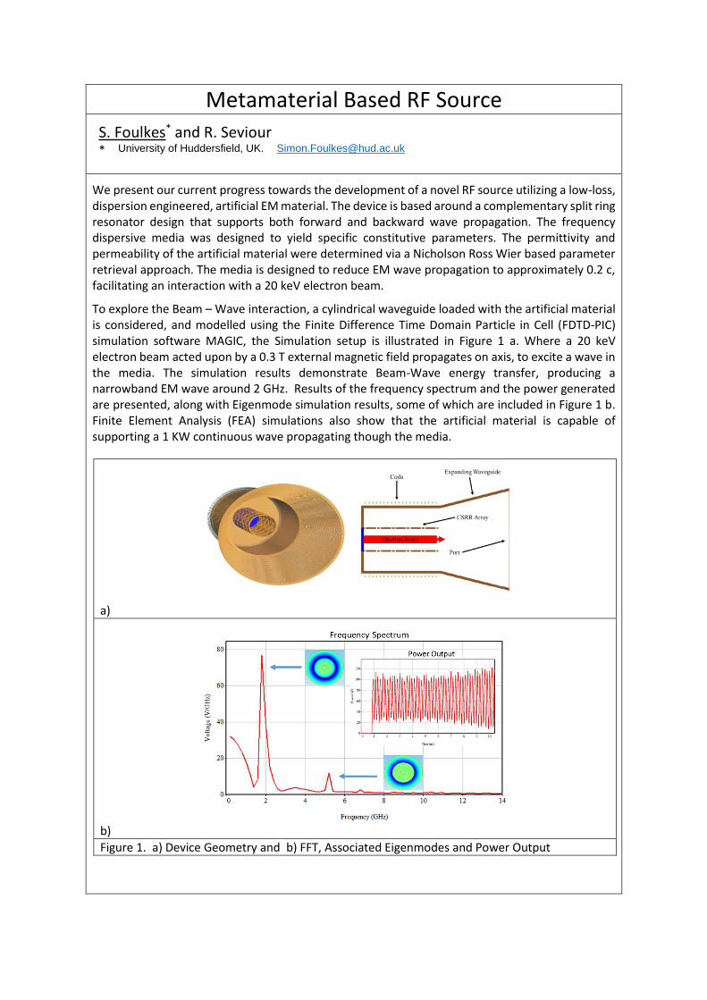
Metamaterial Based RF Source
S. Foulkes* and R. Seviour
* University of Huddersfield, UK. [email protected]
We present our current progress towards the development of a novel RF source utilizing a low-loss, dispersion engineered, artificial EM material. The device is based around a complementary split ring resonator design that supports both forward and backward wave propagation. The frequency dispersive media was designed to yield specific constitutive parameters. The permittivity and permeability of the artificial material were determined via a Nicholson Ross Wier based parameter retrieval approach. The media is designed to reduce EM wave propagation to approximately 0.2 c, facilitating an interaction with a 20 keV electron beam.
To explore the Beam – Wave interaction, a cylindrical waveguide loaded with the artificial material is considered, and modelled using the Finite Difference Time Domain Particle in Cell (FDTD-PIC) simulation software MAGIC, the Simulation setup is illustrated in Figure 1 a. Where a 20 keV electron beam acted upon by a 0.3 T external magnetic field propagates on axis, to excite a wave in the media. The simulation results demonstrate Beam-Wave energy transfer, producing a narrowband EM wave around 2 GHz. Results of the frequency spectrum and the power generated are presented, along with Eigenmode simulation results, some of which are included in Figure 1 b. Finite Element Analysis (FEA) simulations also show that the artificial material is capable of supporting a 1 KW continuous wave propagating though the media.
a)
b)
Figure 1. a) Device Geometry and b) FFT, Associated Eigenmodes and Power Output

Design of 0.365-THz backward wave oscillators using SDG/FWG SWS and Sheet Beam
Jin Zhang1, Liang Zhang2, Tianzhong Zhang1, Yasir Alfadhl1, Xiaodong Chen1, Jie Xie2 and Adrian W. Cross2
1School of Electronic Engineering and Computer Science, Queen Mary University of London, London E1 4NS, UK. [email protected]
2Department of Physics, University of Strathclyde, Glasgow G1 1XQ, UK
3College of Electronic Science and Technology, Shenzhen University, Shenzhen 518061, China
Abstract: Terahertz is a promising technology with potential applications in various fields, such as safety monitoring for detecting hidden explosives and drugs, medical imaging [1], communications [2], electron paramagnetic resonance (EPR) [3], etc. Demand for high-power, compact THz sources has been growing due to these applications. The solid-state sources can only generate THz waves with lower power. Conventional VEDs, such as gyrotrons, free-electron lasers (FELs) could generate much higher power, but require very strong magnetic field or high-energy electron beam, making them difficult to have a compact size. Therefore, it is desirable to develop THz sources with high power and compactness.
A pseudospark plasma cathode can generate a sheet electron beam with very high current, and the capability of self-focusing, thus exterminating the necessity of the focusing magnetic field, which makes it an outstanding candidate to be used in VED THz sources with high power and compactness [4]. Hence, we have designed backward wave oscillators (BWOs) using a staggered double grating (SDG) SWS/ folded waveguide (FWG) SWS with a sheet beam generated by a pseudospark cathode, as shown in Fig. 1, in which the SDG BWO and the FWG BWO are represented by Fig. 1(a) and Fig. 1(b), respectively.
(a) (b)
Fig. 1 BWO models: (a) SDG BWO; (b) FWG BWO
(a) (b)
Fig. 2 Output power of the BWOs: (a) SDG BWO; (b) FWG BWO
PIC simulation is performed for the BWOs with SDG/FWG, respectively, with beam current density ranging from 1×10⁷A/m2 to 3×10⁷A/m2, and the output power is shown in Fig. 2. Fig. 2(a) shows that the power of the SDG BWO increases as the beam current density grows, and the maximum power is 2706 W at 31 kV (J=3×10⁷A/m2); there is a power gap from at ~ 32 kV. Fig. 2(b) shows that the power of the FWG BWO also increases with the beam current density, and the maximum power is 479 W at 35 kV (J=3×10⁷A/m2). The SDG BWO works in a dual-band mode due to the power gap, while the working frequency band of the FWG BWO is continuous (365-371 GHz). It can be concluded that significant output power is obtained from the BWOs using SDG/FWG and pseudospark cathode, posing them as a promising THz sources. References: [1] M. Tonouchi, “Cutting-edge terahertz technology,” Nature photonics, 1(2), pp. 97-105, 2007. [2] A. Hirata, et al., “120-GHz-band millimeter-wave photonic wireless link for 10-Gb/s data transmission,” IEEE Trans. Microwave Theory Technol, 54(5), pp. 1937–1944, 2006. [3] M. Pannier, S. Veit, A. Godt, G. Jeschke, H. W. Spiess, “Dead-time free measurement of dipole–dipole interactions between electron spins,” Journal of Magnetic Resonance, 142(2), pp.331-340, 2000. [4] Y. Yin, et al., “Simulation and Experiments of a W-Band Extended Interaction Oscillator Based on a Pseudospark-Sourced Electron Beam,” IEEE Trans. Electron Devices, 63(1), pp.512-516, 2015.
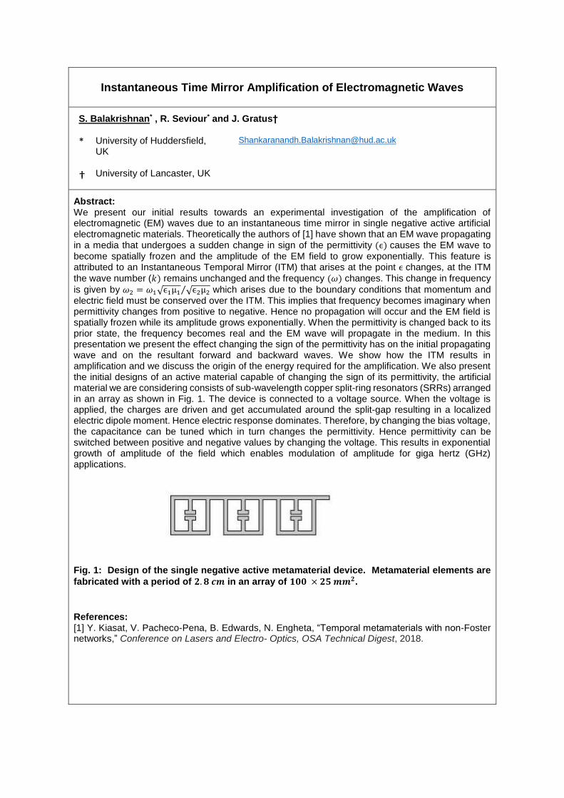
Instantaneous Time Mirror Amplification of Electromagnetic Waves
S. Balakrishnan* , R. Seviour* and J. Gratus†
* University of Huddersfield, UK
† University of Lancaster, UK
Abstract: We present our initial results towards an experimental investigation of the amplification of electromagnetic (EM) waves due to an instantaneous time mirror in single negative active artificial electromagnetic materials. Theoretically the authors of [1] have shown that an EM wave propagating in a media that undergoes a sudden change in sign of the permittivity (ϵ) causes the EM wave to become spatially frozen and the amplitude of the EM field to grow exponentially. This feature is attributed to an Instantaneous Temporal Mirror (ITM) that arises at the point ϵ changes, at the ITM
the wave number (𝑘) remains unchanged and the frequency (𝜔) changes. This change in frequency
is given by 𝜔2 = 𝜔1√ϵ1µ1 √ϵ2µ2⁄ which arises due to the boundary conditions that momentum and electric field must be conserved over the ITM. This implies that frequency becomes imaginary when permittivity changes from positive to negative. Hence no propagation will occur and the EM field is spatially frozen while its amplitude grows exponentially. When the permittivity is changed back to its prior state, the frequency becomes real and the EM wave will propagate in the medium. In this presentation we present the effect changing the sign of the permittivity has on the initial propagating wave and on the resultant forward and backward waves. We show how the ITM results in amplification and we discuss the origin of the energy required for the amplification. We also present the initial designs of an active material capable of changing the sign of its permittivity, the artificial material we are considering consists of sub-wavelength copper split-ring resonators (SRRs) arranged in an array as shown in Fig. 1. The device is connected to a voltage source. When the voltage is applied, the charges are driven and get accumulated around the split-gap resulting in a localized electric dipole moment. Hence electric response dominates. Therefore, by changing the bias voltage, the capacitance can be tuned which in turn changes the permittivity. Hence permittivity can be switched between positive and negative values by changing the voltage. This results in exponential growth of amplitude of the field which enables modulation of amplitude for giga hertz (GHz) applications.
Fig. 1: Design of the single negative active metamaterial device. Metamaterial elements are
fabricated with a period of 𝟐. 𝟖 𝒄𝒎 in an array of 𝟏𝟎𝟎 × 𝟐𝟓 𝒎𝒎𝟐.
References: [1] Y. Kiasat, V. Pacheco-Pena, B. Edwards, N. Engheta, “Temporal metamaterials with non-Foster networks,” Conference on Lasers and Electro- Optics, OSA Technical Digest, 2018.

The State of the Art in Solid-State Power Generation at RF and Microwave Frequencies
J.L.B.Walker*
*Integra Technologies, Inc., USA. [email protected]
Abstract: This paper will detail the state-of-the-art in RF and microwave power generation using Si and GaN power transistors for pulsed applications with power levels >1kW. The merits and drawbacks of the various transistor technologies for RF power generation will be described in terms of voltage, current, efficiency, thermal, bandwidth, impedance and VSWR ruggedness limitations.
It will be shown that GaN High Electron Mobility Transistors (HEMT) offer significant advantages over other technologies for high-power pulsed applications (but not necessarily for CW applications), and the latest advances in this technology that achieve multi-kW level output power using drain voltages of 100-150V will be described.
Finally, the various methods of combining RF power transistors (circuit, cavity, free-space etc) will be reviewed and it will be shown that it is now feasible to generate 100’s of kW at UHF and 10’s of kW at microwave frequencies using a combination of GaN HEMT transistors and power combining. Examples of some state-of-the-art transistors and amplifiers will be given.

Design and simulation of a 0.37 THz gyro-TWA
Liang Zhang*, Craig R. Donaldson*, Wenlong He†, Kevin Ronald*, Alan D. R. Phelps*, and Adrian W. Cross*
*Department of Physics, SUPA, University of Strathclyde, Glasgow G4 0NG, Scotland, UK
†College of Electronic Science and Technology, Shenzhen University, Shenzhen, 518060, China
Abstract: This paper reports the work being carried out to realize a gyrotron-traveling wave amplifier (gyro-TWA) operating at 372 GHz based on a helically corrugated interaction region (HCIR). The schematic of the gyro-TWA is shown in Fig. 1.
The beam-wave interaction will be driven by an electron beam produced by a cusp gun [3] and traveling through a helically corrugated interaction region (HCIR) with a magnetic field of 7.3 T. A cryogenic-free superconducting magnet (SCM), as shown in Fig. 1, will provide the required field. The HCIR enables a favorable dispersion characteristic allowing for even more broadband amplification, higher power capabilities, reduced effect of electron beam velocity spread and a second harmonic interaction [4]. Further waveguide components will be required such as a circular polarizer (5) [5], input (3) [6] and output couplers (8) [7] and microwave windows (3,9) [8], see Fig. 2. This paper will present the design of the gyro-TWA, its components with particular focus on the design and measurement of the HCIR.
Fig. 1. Schematic of the gyro-TWA.
References: [1] W. He, C. R. Donaldson, L. Zhang, et al., "Broadband Amplification of Low-Terahertz Signals Using Axis-Encircling Electrons in a Helically Corrugated Interaction Region," Phys. Rev. Lett., vol. 119, no. 18, p. 184801, 2017. DOI: 10.1103/PhysRevLett.119.184801

The Accurate Prediction of Longitudinal Electromagnetic Mode Profile Sculpting inWire Media using Concepts of Spatial Dispersion.
J. Gratus1,3,5, T. Boyd1,3, P. Kinsler1,3, R. Letizia2,3, R. Seviour4
1 Department of Physics, Lancaster University, Lancaster LA1 4YB, UK2Department of Engineering, Lancaster University, Lancaster LA1 4YR, UK3Cockcroft Institute, Keckwick Lane, Daresbury, Warrington WA4 4AD, UK
4 School of Computing and Engineering, Ion Beam Centre, Centre for Engineering Materials, HuddersfieldHD2 3DH
Abstract – Using a wire medium with high dielectric wires of varying radius, we can sculptthe longitudinal electromagnetic wave profile. Such sculpted wave profiles have applicationsin signal processing and accelerator physics. The required design modulation of the wires wascalculated using concepts of spatial dispersion, and full 3D CST Studio simulations of the struc-tures were run. Predictions and simulations were in excellent agreement, validating our designprocess.
12L L 3
2L 2L0
1
−1
E
z
(a) Flatter
12L L 3
2L 2L0
1
−1
E
z
(b) Peakier
12L L 3
2L 2L0
1
−1
E
z
(c) Triangular
Fig. 1: Solutions to Mathieu’s equations showing (a) flatter, (b) peakier and (c) triangular profiles
I. MODE PROFILE SCULPTING
In a uniform waveguide the mode profiles along the propagation axis are sinusoidal. Here we consider methodsof customising this wave profile, a process with many possible applications [1, 2, 3, 4, 5]. For example a flatterprofile like that in figure 1(a) enables us to reduce non linear effects. Further, when controlling the bunch propertiesin particle accelerators, it would mean that more of the bunch receives the same energy boost, so that it could be
Fig. 2: A medium consisting of parallel wires of varying radii. The shape of the wire was calculated in order toexcite the Mathieu functions in figure 1. We consider infinite media by using periodic boundary conditions, but alsohave done simulations of finite media when considering device-like cases; typical finite simulations incorporated10 longitudinal periods.
1

Fig. 3: CST simulations of the electric field for a wire medium with fixed radius. This field has the desiredproperties. (Right) The strength of the electric field as one passes along a line through the wire.
used to accelerate longer bunches. In contrast, a peakier profile such as that in fig. 1(b) could be used to enhancesnonlinear effects; it would also enhance the signal to noise ratio. In accelerators, it would help in the accelerationof short bunches. Another example is the triangular profile in fig. 1(c), which gives a longer bunch a sustainedchirp. Further, this wave profile shaping could have utility in high harmonic generation [6]. Existing methods ofmode profile shaping include varying the geometry of the waveguide and adding multiple sinusoidal modes.
We consider longitudinal modes in a wire medium with varying radii, figure 2. This is driven by the applicationin particle accelerators. Inspired by [7, 8] we initially looked for longitudinal modes in copper wire media. How-ever, being unable to find any initially (a result consistent with [7, 8]), we instead looked for longitudinal modesin high dielectric wire media [9, 10]. We modelled the three dimensional wire medium using a one dimensionalspatially dispersive medium with permittivity of the form
εr(ω, k) = 1 +ω2
P
−ω2 + k2 + ω20
(1)
There exist solutions of the form E = Ee−iω t+ikzk, D = 0 and B = 0, so that εr(ω, k) = 0. I.e. it is an ENZmedium and the dispersion relation is
ω2 − k2 = ω2P + ω2
0 (2)
We used CST Microwave studio to examine the modes in a uniform wire. This revealed a large number of differentmodes, with a great range of mode profiles and dispersion properties. A detailed and exhaustive search thoughthese possibilities showed that some of them had the desired properties. It turns out a good case was when thewires are thin and have high εr. We set period ∆x = 11mm, ∆y = 15mm, ∆z = 52mm and εr = 1200. Periodicboundary conditions κx = κy = 360◦, varying κz between 0 and 180◦. The wire diameter were around 2mm. Thewires were in the z-direction. One such is shown in figure 3, in which we can see that:
• The field away between the wires was longitudinal, a crucial feature needed for on-axis particle acceleration• Most of the field was between the wires, where it is needed; it is not a localised mode trapped on the wire(s).• The dispersion relation is given by (2) to a high degree of accuracy.• One could control this dispersion by varying the thickness of the wires.
Note that, by making the radius depend on position, we have a permittivity that depends both on position zand wave-number k. Since these on Fourier transform conjugate variable this raises interesting issues [2, 11]. Wehandle it here by taking the Fourier transform of (2) where Λ(r) = ω2
P + ω20 .
E′′ + ω2 E = Λ(r)E (3)
We can now make the radius a function of position to give
E′′ +(ω2 − Λ
(r(z)
))E = 0 (4)
By suitable choice of r(z) we can construct the various Mathieu equations.Frequency domain CST simulation were made with the varying wire for the flat, peakier and triangular profiles
with very good agreement. The flat profile is shown in figure 4 and the peakier profile in figure 5.
2

Fig. 4: Flat profile: 3D fields from CST simulations (left), and a comparison of predicted (red) and simulated(black) longitudinal electric fields.
Fig. 5: The predicted (red) and CST simulated longitudinal electric field (black) for the peakier profile.
II. CONCLUSION
We have shown it is possible to sculpt the electric field for longitudinal modes in a wire medium. The resultswere very close to those predicted using a 1-dimensional spatially dispersive medium. These are exciting resultand we aim to verify these modes experimentally.
3
ACKNOWLEDGEMENT
The authors are grateful for the support provided by STFC (the Cockcroft Institute ST/G008248/1), EPSRC (theAlpha-X project EP/J018171/1 and EP/N028694/1) and the Lancaster University Faculty of Science and Technol-ogy studentship program. Figures 3, 4 and 5 are used with kind permission from [12]
REFERENCES
[1] “Spatially dispersive inhomogeneous dielectric wire media with periodic structure.” Gratus J., Letizia R.,M. McCormack. PIERS 2015 Proceedings.
[2] “Spatially dispersive inhomogeneous electromagnetic media with periodic structure.” Gratus J., M. McCor-mack. J. Optics, 17(2):025105, 2015.
[3] “Electromagnetic mode profile shaping in waveguides.” Gratus J., Kinsler P., Letizia R., Boyd T. EMTS2016Proceedings
[4] “Electromagnetic mode profile shaping in waveguides.” Gratus J., Kinsler P., Letizia R., Boyd T. Appl. Phys.A (2017) 123: 108.
[5] “Customised Mode Profiles Using Functional Materials.” Gratus J., Kinsler P., Letizia R., Boyd T. Journal ofoptics (In review)
[6] “Carrier-wave self-steepening & applications to HHG,” Radnor, S., et al, Phys. Rev. A Vol. 77, 033806 2008.
[7] Joao T Costa and Mario G Silveirinha. Macroscopic electromagnetic response of arbitrarily shaped spatiallydispersive bodies formed by metallic wires. Physical Review B, 86(7):075129, 2012.
[8] Wei Song, Zhun Yang, Xin-Qing Sheng, and Yang Hao. Accurate modeling of high order spatial dispersion ofwire medium. Optics express, 21(24):29836–29846, 2013.
[9] “Phase diagram for the transition from photonic crystals to dielectric metamaterials”. Rybin, M. V. et al. Nat.Commun. 6:10102 doi: 10.1038/ncomms10102 (2015).
[10] “Magnetic hyperbolic metamaterial of high-index nanowires.” Mirmoosa, M. S., S. Yu Kosulnikov, and C. R.Simovski. Physical Review B, 94(7):075138 (2016).
[11] “Covariant constitutive relations and relativistic inhomogeneous plasmas.” Gratus J., Tucker R. Journal ofMathematical Physics 52, No. 4, 042901, 04. (2011).
[12] “Customised Mode Profiles” Gratus J., Kinsler P., Letizia R., Boyd T. Lancaster internal report.
4

Multi-Gigabit Wireless Links using Resonant Tunneling Diode
J. Wang, A. Al-Khalidi and E. Wasige
High Frequency Electronics Group, School of Engineering, University of Glasgow
Abstract: There is great demand for ultra-high speed wireless communication especially with the development of modern multimedia technology. Instead of improving spectral efficiency by using advanced modulation schemes and complex signal processing techniques, the other approach is to move to unregulated spectrum in millimetre-wave (mm-wave) or terahertz (THz) frequency range for higher bandwidth. Resonant tunnelling diode (RTD) is the fastest solid-state device with a fundamental frequency of oscillations of around 2 THz recently demonstrated [1].
The core of an RTD device comprises a double barrier quantum well (DBQW) epitaxial layer structure which consists of a narrow band gap (Eg) epilayer (InGaAs) sandwiched between two thin wide bandgap epilayers (AlAs). The measured I-V characteristics for single RTD with device size 16 μm2 is shown in Fig. 1. The peak current density is 187 kA/cm2 and the peak to valley current ratio (PVCR) being about 2.5. In this paper we present a monolithic microwave integrated circuit (MMIC) that combines two resonant tunnelling diodes (RTDs) in parallel as shown in Fig. 2. Re was realized as a thin film resistor. The decoupling capacitor Ce and DC block capacitor Cb was fabricated by using metal-insulator-metal (MIM) capacitor. The inductor L is realized by a coplanar waveguide (CPW) transmission line with length of
𝑙 terminated by Ce. The oscillators were measured on-wafer. The measurement results are summarized in Table I. It is worth to note that the output powers are reported here directly from RTD oscillators without any power amplifier stage. 2 mW at 84 GHz and 1 mW at 206 GHz which are the highest power reported for RTD-based oscillators in the relative frequency range. Effort has been devoted to package both W and J band RTD oscillator. The W-band waveguide packaged device is shown in Fig. 3. By using mW RTD as transmitter (Tx), 15Gbps using W-band RTD Tx over 50cm distance was demonstrated. The bit error rate (BER) was also characterized as 1.0×10⁻⁶ up to 5 Gbps, 3.6×10⁻⁴ @10 Gbps, and 4.1×10⁻³ @15 Gbps. By using J-band RTD Tx, 6 Gbps error-free and 20 Gbps with correctable BER with ranges of up to 20 meters was also demonstrated. The block diagram and lab measurement setup are illustrated in Fig. 4 and Fig. 5. The transmitter (Tx) consists of a voltage controlled RTD oscillator (RTD-VCO) with a horn antenna. No power amplifier (PA) is employed at this stage which shows the simplicity/merit of RTD transmitter. The data is superimposed over DC bias through a bias tee. The modulation scheme is ASK. On the receiver (Rx) side, the received signal and demodulated by a Schottky barrier diode (SBD) envelope detector and then the baseband data is amplified by a low noise amplifier (LNA) and displayed on oscilloscope. The 10Gbps and 15 Gbps eye diagram are shown in Fig. 6 and Fig. 7.
The work reported here demonstrates the potential of RTD oscillators for applications as compact sources for multi-gigabit wireless communication systems. The RTD transmitters provide a very promising simple, low cost, compact solution for future ultra-fast wireless communication systems. Future work is focused on RTD epitaxial layer design to increase the oscillator output power at THz frequencies, the development of integrated modulators and RTD based receivers for numerous applications.
Table I: Summary of RTD oscillators performance
Device size (μm2)
Fundamental Freq. (GHz)
Power (mW)
DC Power (mW)
5x5 50 10 120
5×5 84 2 114
4×4 260 1 180
4×4 308 0.5 191
References: [1] T. Maekawa, H. Kanaya, S. Suzuki, and M. Asada, “Oscillation up to 1.92 THz in resonant tunneling diode by reduced conduction loss,” Appl. Phys. Expr., Vol. 9, No. 2, p. 24101, 2016.

Fig. 1. Measured and modeled device IV
characteristics. The negative differential conductance Gn is also shown. Note that the Gn
is negative across the entire NDR region with a
minimum value of -42.5 mS.
Fig. 1.
Fig. 2. Fabricated double RTD oscillator.
2RTDs are connected in parallel. Each device is biased individually with resistor Re and bypass
capacitor Ce. Cb is the DC block capacitor. The
CPW length 𝑙 depends on the designed frequency.
Fig. 3. Packaged W-band
RTD transmitter.
Fig. 4. Block diagram of the wireless communication
measurement setup Fig. 5. W-band wireless communication measurement setup
in the lab
Fig. 6. 10 Gbps ASK eye diagram: when RTD is based at 1.2
V with data amplitude 400 mV.
Fig. 7. 15 Gbps ASK eye diagram: when RTD is based at 1.2
V with data amplitude 400 mV.

Review of a W-band TWT for Satellite Communications
C.W. Robertson(1), K. Ronald(1), C. Gilmour(2), D. Dyson(2), P. Huggard(3), M. Beardsley(3), F. Cahill(3), R. Dionisio(4)
(1) SUPA and the Department of Physics, John Anderson Building,
107 Rottenrow, University of Strathclyde
Glasgow, G4 0NG, UK
(2)TMD Technologies, Swallowfield Way, Hayes
Middlesex, UB3 1DQ, UK
(3)RAL Space, STFC Rutherford-Appleton Laboratory,
Harwell Campus, Didcot, Oxfordshire, OX11 0QX, UK
(4)ESA ESTEC
Keplerlaan 1, 2201 AZ Noordwijk, NL
Abstract:
We present a review on the progress on a project to design, fabricate and test a 71-76GHz, ~100W, 40dB gain TWT
to validate key technologies for space communications (ESA contract No. 4000119380/17/NL/HK/hh).
Predictions of the performance of the amplifier have been obtained using the PIC method in CST studio. These have
studied the amplifiers gain and saturated efficiency/power as a function of frequency and microwave input power.
The simulations have mapped the transition from the linear to the saturated regime of operation showing the
performance varies with frequency. Further studies of critical factors such as multipacting, thermal/ mechanical
loading of the structure have also been carried out, however no significant impact on performance has been
observed. PPM stack and electron gun designs have been carried-out by TMD Technologies. These have shown
effective formation and transport of the required electron beam within the limited transverse size of the beam
tunnel.
A high frequency window has been designed using CST microwave studio to carry-out S-parameter analysis with the
goal of achieving return losses of 30dB or better over the frequency range of interest. A review of the fabrication and
resulting performance of this high frequency window will also be reported.
References: [1] Nguyen, K.T., et al., Design Methodology and Experimental Verification of Serpentine/Folded-Waveguide TWTs. IEEE Transactions on
Electron Devices, 2014. 61(6): p. 1679-1686
[2] Booske, J.H., et al., Accurate parametric modeling of folded waveguide circuits for millimeter-wave traveling wave tubes. IEEE Transactions on Electron Devices, 2005. 52(5): p. 685-694
[3] Gilmour, Principles of traveling wave tubes, ISBN 0-89006-720-1, Artech House, 1994
[4] A.M. Cook et.al. IEEE transactions on electron devices, vol.60, no.3, march 2013

Asymmetric SRF dual axis cavity for ERLs: studies and design for ultimate performance and applications
I. V. Konoplev1, Ya. Shashkov2, F. Marhauser3
1 JAI, Department of Physics, University of Oxford, Oxford, OX1 3RH, UK.
2 National Research Nuclear University MEPhI, Moscow, Russia
3 Thomas Jefferson National Accelerator Facility, Newport News, VA 23606, USA
Abstract:
A dual axis asymmetric SCRF ERL has been recently proposed as a possible way to drive a high average current electron beam while avoiding the BBU instability excitation. Such high current ERLs can be attractive for the next generation light sources, beam cooling in electron ion collider and isotope production. Here the results of the studies of band-pass modes and HOMs will be shown. The field distribution of the modes will be shown and asymmetric field distribution of HOMs will be demonstrated and HOMs excitations using dipole couplers will be discussed. The original design of the dual axis asymmetric cavity has been optimised to minimize the peaks of magnetic and electric fields on the cavity surface, to increase the distance between operating mode and neighbouring parasitic mode as well as to reduce the cavity manufacturing cost. To reach the goals several solutions have been suggested leading to simplification of the manufacturing as well as bringing the fields amplitudes on the cavity surface to the acceptable values. The new design of the cavity will be presented and possible applications of such a high-current ERL will be discussed.

Extending our successful field profile shaping method to different realisations of wire media
T. Boyd1, 4, 5, J. Gratus1, 4, P. Kinsler1, 4, R. Letizia2, 4 , R. Serviour3
1Department of Physics, Lancaster University, Lancaster, LA1 4YW, UK
2Department of Engineering, Lancaster University, Lancaster, LA1 4YW, UK
3School of Computing and Engineering, Huddersfield University, Huddersfield, HD2 3DH, UK
4Cockcroft Institute, Keckwick Lane, Daresbury, Warrington, WA4 4AD, UK
Abstract: We have previously demonstrated in simulations of infinite dielectric wire media that our method can successfully replicate desired profiles [1]. Here we will cover the extension of this method to other, more practical realisations, of wire media as well as efforts, such as time domain simulations, made to bolster these results. This work has given us more confidence on the ability of this method to be experimentally replicated.
Electromagnetic field shaping The ability to control how the field strength of an electromagnetic field varies spatially is a useful skill. Crab cavities are currently used to achieve such an effect to facilitate control of the particle bunch in accelerators [2]. Our method allows for a high level of control over the field profile-the spatial variation of field strength-without the need to iteratively optimise the structure, as is done for crab cavity design. When a suitable profile is chosen our method produces a set of parameters for the structure which if implemented will instantly support the desired profile without the need for further refinement.
Fig. 1 A representation of a wire medium Fig. 2 Typical field profiling results obtained The structure we have worked with is a modified version of a standard dielectric wire medium, similar to the one shown in Fig. 1; ordinary wire media consist of a lattice of constant radius, identical, parallel dielectric wires. Such structures are useful because they can be described as a one-dimensional, spatially dispersive, inhomogeneous medium - the effective permittivity depends not only on frequency (temporal dispersion) but also the wavenumber 𝑘 [3]. Using this model we can predict the existence of purely longitudinal electric modes with a plasma-like dispersion relation, and these modes are integral to our electromagnetic field profile shaping scheme. Our field profile shaping method exploits our ability to control the cut-off frequency of these modes,𝜆𝑠, by varying the wire radius, 𝑟. As such the relationship
between these two parameters as defined by 𝜆𝑠(𝑟) is extremely important. Extending our method to new regimes We had demonstrated the ability to closely replicate a desired profile, as shown in Fig. 2, but these initial results were achieved for a specific realisation of wire media. This realisation consisted of an infinite lattice of dielectric wires, or rods, with an extremely high permittivity, 𝜀𝑟 = 1600. Although these material properties are achievable using barium-strontium-titanate (BST), the specificity of this initial realisation raised concerns about the flexibility of our method. To alleviate these concerns, we then extended our method to a number of new regimes. One area we explored was the effect of the wire permittivity. We found that the relationship 𝜆𝑠(𝑟) for each permittivity examined was of the same form and as such we were able to successfully use our method to replicate desired field profiles. The relationships for each of these permittivity values is plotted in Fig. 3 along with the exponential decay fitting curve used to describe the relationship.
References: [1] G. Schmidt, “Nonadiabatic particle motion in axialsymmetric fields,” Phys. Fluids, 21, pp. 2354-2364,

Fig. 3 The 𝜆𝑠(𝑟) relationship for a variety of permittivity values
As well as the wire permittivity we have considered the effect of the lattice parameters and the introduction of perturbations in our infinite structures. Another significant step we have made in extending our method is the consideration of finite structures. Clearly infinite wire media are not practically realisable so it is useful to explore the use of finite structures. As with the infinite case, we found that the 𝜆𝑠(𝑟) relationship for finite dielectric wire media is well described by an exponential decay curve and using this we are able to vary the radius to produce a desired field profile.
With finite structures successfully simulated were then able to move to time domain simulations of wire media. Using finite lattice structures, we simulated the excitation of the structure through a port mode. In these extended structures it was necessary to evaluate the resulting field profile at a number of different position, which spanned from the bottom of the structure near the excitation port to the top of the structure. A plot of a figure of merit for the agreement between the observed field profile and the desired field profile against position is shown in Fig. 4. An 𝑅2 value close to 1 represents a field profile that is extremely close to the desired profile. From Fig. 4 we can see that there are large reasons of the structure where the agreement is very good, the brown and orange squares, and some others where it is quite poor, the magnet square. This work could be further improved by an analysis of the transmission of these fields.
Conclusion
We have detailed the steps we have taken to extend our successful field profile shaping method to a variety of different regimes. This has included different permittivity values, finite wire media structures and an exploration of the possibility of exciting the profiled fields in time domain simulations.
References
[1] Boyd, Taylor, Jonathan Gratus, Paul Kinsler, and Rosa Letizia. "Customizing longitudinal electric field profiles using spatial dispersion in dielectric wire arrays." Optics express 26, no. 3 (2018): 2478-2494.
[2] Verdú-Andrés, Silvia, Sergey Belomestnykh, Ilan Ben-Zvi, Rama Calaga, Qiong Wu, and Binping Xiao. "Crab cavities for colliders: past, present and future." Nuclear and particle physics proceedings 273 (2016): 193-197.
[3] Belov, P. A., R. Marques, S. I. Maslovski, I. S. Nefedov, M. Silveirinha, C. R. Simovski, and S. A. Tretyakov. "Strong spatial dispersion in wire media in the very large wavelength limit." Physical Review B 67, no. 11 (2003): 113103.

RF Analysis of the Load Lock Photocathode Injector Upgrade for the 10Hz Repetition Rate CLARA Gun
A.J. Gilfellon*
*STFC, ASTeC, Daresbury Laboratory, WA4 4AD, UK. [email protected]
Abstract:
CLARA (Compact Linear Accelerator for Research and Applications) is a FEL test-bed accelerator located at Daresbury Laboratory in the North-West of England. As well as being a precursor for a cutting-edge FEL facility based in the UK, CLARA also seeks to greatly contribute to international research and knowledge in the subject area. Starting in April this year, CLARA has undergone a series of maintenance procedures and upgrades as part of a scheduled shutdown period, one timetabled upgrade was the replacement of the backplate/photocathode of the 10Hz rep rate gun with a new backplate that included an integrated load lock system, designed to facilitate the more rapid and less intrusive exchange of photocathodes. In this talk I highlight the installation of the load lock backplate and RF characterisation of the upgraded gun, including beadpull experiments that were used to determine the field flatness, stability and reproducibility analyses of photocathode extraction / re-insertion and the effects that baking procedures (needed for various cleaning processes) had on the resonant π mode frequency and Q0. In addition to this, I discuss the nature and results of simulations that were carried out to deliver an estimate of the momentum the beam can expect to obtain, see figure 1 below.
Figure 1: A plot of z-axis coordinate vs. electric field strength in the second CST MWS simulation. The Peak E-field value, marked as a black cross, and the field flatness was found to be 21.260 kV/m and 98.9% respectively. The inserted subplot is an expanded view of the data showing the slight phase difference between Re(E) and the Im(E) which leads to the situation where | E | never obtains a z-axis zero value within the gun. The | E | data was processed and used as the input for the subsequent ASTRA simulation in order to evaluate the expected beam momentum.

Implications of beam filling patterns on the design of recirculating energy recovery linacs
R. Apsimon*†, S. Setiniyaz*†, and P. Williams†
*Engineering Department, Lancaster University, LA1 4YW, UK
†Cockcroft Institute, Daresbury Laboratory, Warrington, WA4 4AD, UK
Abstract:
Recirculating energy recovery linacs are a promising technology for being able to deliver high power particle beams (~GW) while only requiring low power (~kW) RF sources. This is achieved by decelerating the used bunches and using the energy they deposit in the accelerating structures to accelerate new bunches. We present studies of the impact of the bunch train filling pattern on the performance of the accelerating RF system. We show that different filling patterns are optimal for different figures of merit, such as RF stability and beam break-up instability. We also present a mathematical description to allow us to identify optimal beam filling patterns under different conditions. The results of these studies have major implications for design constraints for future energy recovery linacs, by providing a quantitative metric for different machine designs and topologies.

The pulsed DC large electrode system for breakdown studies at CERN
R.C. Peacock*†, G.C. Burt*, I. Profatilova†, W. Wuensch†
*Lancaster University, Lancaster, United Kingdom
†CERN, Geneva, Switzerland
Abstract: CLIC (Compact Linear Collider) is the concept for a future linear electron-positron high gradient collider based at CERN. One of the problems related to running high gradients accelerators is a phenomenon called vacuum breakdown. Vacuum breakdown in an accelerator is when an electrical connection is made between the electron beam and the walls of the accelerator. There are several theories as to what could cause breakdown but currently the exact process that causes it to occur is unknown. Due to the complexity of linear accelerators, to simplify analysis breakdown is also studied in DC systems. This talk is based on the Pulsed DC systems, designed for the of study vacuum breakdown phenomenon and conditioning processes. In the systems, two plane electrodes with large surface areas are placed parallel to each other with a separation between 20 and 100 micrometres, under a high vacuum. The pulsed DC system is capable of running at high repetition rates, at a relatively low cost compared to RF due to the reduced amount of power required in this setup. Providing experimental results from field emission current measurements, conditioning of different materials and the effect of different parameter changes to the breakdown rate and the material properties. Also, looking at the current methods of detecting breakdowns and current analysis using a spectrometer.


Notes ________________________________________________________________________________________________________
________________________________________________________________________________________________________
________________________________________________________________________________________________________
________________________________________________________________________________________________________
________________________________________________________________________________________________________
________________________________________________________________________________________________________
________________________________________________________________________________________________________
________________________________________________________________________________________________________
________________________________________________________________________________________________________
________________________________________________________________________________________________________
________________________________________________________________________________________________________
________________________________________________________________________________________________________
________________________________________________________________________________________________________
________________________________________________________________________________________________________
________________________________________________________________________________________________________
________________________________________________________________________________________________________
________________________________________________________________________________________________________
________________________________________________________________________________________________________
________________________________________________________________________________________________________
________________________________________________________________________________________________________
________________________________________________________________________________________________________
________________________________________________________________________________________________________
________________________________________________________________________________________________________
________________________________________________________________________________________________________
________________________________________________________________________________________________________
________________________________________________________________________________________________________
________________________________________________________________________________________________________
________________________________________________________________________________________________________
________________________________________________________________________________________________________

