natarajan, chandra m, tanner, michael g, and hadfield, …eprints.gla.ac.uk/73961/1/73961.pdf ·...
TRANSCRIPT
Natarajan, Chandra M, Tanner, Michael G, and Hadfield, Robert (2012) Superconducting nanowire single-photon detectors: physics and applications. Superconductor Science and Technology, 25 (6). 063001. ISSN 0953-2048 Copyright © 2012 IOP Publishing Ltd http://eprints.gla.ac.uk/73961 Deposited on:15 January 2013
Enlighten – Research publications by members of the University of Glasgow http://eprints.gla.ac.uk

Superconducting nanowire single-photon detectors: physics and applications
This article has been downloaded from IOPscience. Please scroll down to see the full text article.
2012 Supercond. Sci. Technol. 25 063001
(http://iopscience.iop.org/0953-2048/25/6/063001)
Download details:
IP Address: 130.209.6.42
The article was downloaded on 15/01/2013 at 11:43
Please note that terms and conditions apply.
View the table of contents for this issue, or go to the journal homepage for more
Home Search Collections Journals About Contact us My IOPscience
IOP PUBLISHING SUPERCONDUCTOR SCIENCE AND TECHNOLOGY
Supercond. Sci. Technol. 25 (2012) 063001 (16pp) doi:10.1088/0953-2048/25/6/063001
TOPICAL REVIEW
Superconducting nanowire single-photondetectors: physics and applications
Chandra M Natarajan1,2, Michael G Tanner1 and Robert H Hadfield1
1 Scottish Universities Physics Alliance and School of Engineering and Physical Sciences,Heriot-Watt University, Edinburgh EH14 4AS, UK2 E L Ginzton Laboratory, Stanford University, Stanford, CA 94305, USA
E-mail: [email protected]
Received 26 January 2012, in final form 5 March 2012Published 4 April 2012Online at stacks.iop.org/SUST/25/063001
AbstractSingle-photon detectors based on superconducting nanowires (SSPDs or SNSPDs) haverapidly emerged as a highly promising photon-counting technology for infrared wavelengths.These devices offer high efficiency, low dark counts and excellent timing resolution. In thisreview, we consider the basic SNSPD operating principle and models of device behaviour. Wegive an overview of the evolution of SNSPD device design and the improvements inperformance which have been achieved. We also evaluate device limitations and noisemechanisms. We survey practical refrigeration technologies and optical coupling schemes forSNSPDs. Finally we summarize promising application areas, ranging from quantumcryptography to remote sensing. Our goal is to capture a detailed snapshot of an emergingsuperconducting detector technology on the threshold of maturity.
(Some figures may appear in colour only in the online journal)
Contents
1. Introduction 11.1. Detection of optical radiation with supercon-
ductors 11.2. Single-photon detection: basic principles and
metrics 22. Superconducting nanowire single-photon detectors
(SNSPDs) 22.1. Origins of device concept 22.2. SNSPD device physics 32.3. Evolution of SNSPD devices 52.4. Practical considerations: cooling, optical cou-
pling and device readout 83. Advanced photon-counting applications with SNSPDs 10
3.1. Overview 10
Content from this work may be used under the termsof the Creative Commons Attribution-NonCommercial-
ShareAlike 3.0 licence. Any further distribution of this work must maintainattribution to the author(s) and the title of the work, journal citation and DOI.
3.2. Quantum key distribution (QKD) 103.3. Development of optical quantum computing 103.4. Characterization of quantum emitters 103.5. Classical space-to-ground communications 113.6. Integrated circuit testing 113.7. Fibre temperature sensing 123.8. Time-of-flight depth ranging 12
4. Conclusion 12Acknowledgments 12References 12
1. Introduction
1.1. Detection of optical radiation with superconductors
The remarkable phenomenon of superconductivity wasdiscovered a century ago by Onnes [1]. This breakthroughopened the pathway to a tantalizing range of real-worldapplications. The superconducting state is sensitive to incidentradiation at optical wavelengths [2], and the advent of thin
10953-2048/12/063001+16$33.00 c© 2012 IOP Publishing Ltd Printed in the UK & the USA
Supercond. Sci. Technol. 25 (2012) 063001 Topical Review
film superconductors, microfabrication techniques and lasersources allowed the first superconducting radiation detectorsand bolometers to be demonstrated as referenced in [3].Spurred by the demands of fields such as astronomy, a suiteof single-photon sensitive energy resolving superconductingdetectors have been developed operating at sub-Kelvintemperatures: the superconducting tunnel junction (STJ) [4],the transition edge sensor (TES) [5] and the kinetic inductancedetector (KID) [6].
Just a decade ago a new superconducting deviceconcept was demonstrated by Gol’tsman et al, based on aniobium nitride nanowire [7]. This type of device, knownas the superconducting single-photon detector (SSPD) orsuperconducting nanowire single-photon detector (SNSPD),is single-photon sensitive at visible and infrared wavelengths,with recovery times and timing precision orders of magnitudefaster than existing single-photon detectors based onsuperconducting materials. In addition, this detector operatesat the boiling point of liquid helium (4.2 K), a temperaturenow within reach of rapidly improving closed-cycle coolingtechnology [8]. SNSPDs have excellent potential for time-correlated single-photon counting (TCSPC) [9] in the infraredwavelength regime, where important new applications areemerging. The main competitors in this arena are solid statesingle-photon avalanche photodiodes (SPADs), which havesuperseded bulky photomultipliers (PMTs) [10]. The longwavelength sensitivity of the SNSPD extends far beyond thatof the Si single-photon avalanche photodiode (SPAD) [11]and the SNSPD is superior to the InGaAs SPAD [12] in termsof signal-to-noise ratio. SNSPDs have been the subject ofintense interest over the past decade and many research groupsaround the world have contributed to device development.This review aims to summarize the basic device operatingprinciple, evolution of SNSPD design, refrigeration andmaterials considerations and to give an overview of promisingapplications.
1.2. Single-photon detection: basic principles and metrics
An ideal single-photon detector (SPD) generates an electricalsignal only upon absorption of a photon. The signal level iswell defined above the noise; in the absence of illuminationno electrical signal is returned. In practice, real SPDs havemany non-ideal characteristics and performance metrics mustbe carefully defined. The most obvious performance metricin a SPD is the detection efficiency (η)—the probability thatan output signal is registered when a photon is incident onthe detector. In practice η is lower than 100% and is likely todepend strongly on the wavelength λ of the incident photons.In any real photon-counting experiment, photons can be lostbefore reaching the detector due to absorption, scattering orreflection within the experimental environment—this loss canbe defined as the coupling efficiency (ηcoupling). The detectormaterial and geometry determines the absorption efficiency(ηabsorption). Finally, there may be a non-unity probability thatthe detector generates an output electrical signal after photonabsorption—we define this as the registering probability
(ηregistering). Taking all these contributions into account, theoverall system detection efficiency (ηsde) is
ηsde = ηcoupling × ηabsorption × ηregistering. (1)
The intrinsic device detection efficiency (ηdde) is defined as
ηdde = ηabsorption × ηregistering. (2)
Therefore ηsde and ηdde are only equal for perfect opticalcoupling i.e. ηcoupling = 1. The device detection efficiency,ηdde, is often reported as ‘quantum efficiency’ in the literature.However this term is used with different meanings fordifferent technologies, so ‘device detection efficiency’ willbe used in this text for clarity. Readers should also heedthe following caveat: unfortunately across the published SPDliterature there is no uniform consensus on whether to reportηsde or ηdde. In general, early SPD device demonstrationsreport ηdde, whereas as when SPDs are implemented inactual photon-counting experiments, ηsde is more likely to bereported.
Other performance metrics quantify limitations in SPDperformance. Stray light and electrical noise can alsopotentially mimic the optical signal. These false detectionevents are called dark counts, usually quantified in terms ofa dark count rate (DCR). The timing uncertainty betweenthe arrival of the photon at the SPD (which can be knownextremely precisely with modern optical sources) and thegeneration of the output pulse from the SPD, may set thetiming resolution. This is known as the jitter (1t) of the SPD.In addition, a real SPD will have a finite recovery time (τ )before it is ready to register a subsequent photon—this setsa limit on the theoretical maximum count rate of the SPD(which in practice may be limited by other factors, such asthe readout electronics).
2. Superconducting nanowire single-photondetectors (SNSPDs)
2.1. Origins of device concept
In 1971, a laser was used for the first time to disruptthe superconductivity of Pb films, forming a resistive statethat could not be explained just by heating effects [2].This experiment showed that the energy of the absorbedphotons resulted in a nonequilibrium state, with hot excitedquasiparticles at a higher temperature than the Cooperpairs in the superconductor. Equilibrium is reached viaa sequence of relaxation processes: (i) inelastic scatteringof quasiparticles by electron–electron interactions andelectron–phonon interactions, (ii) generation of quasiparticlesby phonons, (iii) quasiparticle recombination and (iv) energydissipation in to the substrate by the phonon in thesuperconductor. The temporal characteristics of the relaxationdepend on the time constants associated with each ofthese processes. Twenty years later, an elegant approach tounderstanding the nonequilibrium relaxation was developedby studying transient photoimpedence response (TPR)of superconducting films [13]. In a TPR measurementthe superconducting film is approximated as a changing
2
Supercond. Sci. Technol. 25 (2012) 063001 Topical Review
kinetic inductance and the film in the resistive state isapproximated as a photoresistor. A two-temperature modelis used to quantitatively extract the time constants fromthe photoresponse of a superconductor film to an opticalpulse [14]. In this model, the time-dependent temperature ofthe electron subsystem (Te) and phonon subsystem (Tp) areobtained by solving the following coupled linear heat-balanceequations:
cedTe
dt= −
ce
τe−p(Te − Tp)+ P(t),
cpdTp
dt= −
ce
τe−p(Te − Tp)−
cp
τes(Tp − T0)
(3)
where ce and cp are the electron and phonon specific heat,respectively, T0 is the substrate temperature, τe−p is theelectron–phonon interaction time, τes is the phonon escapetime and P(t) is the time-dependent power of radiationabsorbed in the unit volume of the film. This two-temperaturemodel ignores any Joule heating via the bias current. This hot-electron and phonon-heatsink scheme predicts a picosecondphotoresponse from the superconductor [14]. This wasexperimentally verified in NbN [15] and YBa2Cu3O7−δ [16]microbridges. The region of hot electrons or quasiparticlesforming the resistive region in the superconductor isknown as the ‘hotspot’. The hotspot concept was originallydeveloped by Skocpol et al to study self-heating effects insuperconducting microbridges [17]. In 1996, Kadin et al [18]approximated the two-temperature model equations as a heatflow equation:
Cd∂T
∂t= κd∇2T + α(T0 − T) (4)
where d is the thickness of the nanowire, κ is thethermal conductivity, C [C = ce + cp] is the heat capacityof the superconducting film, α is the thermal boundaryconductance between the film and the substrate, T0 is thesubstrate temperature (since the nanowire is thin enough)and the temperature of the nanowire is approximated to onetemperature T . The solutions to equation (4) predict that thephoton-induced hotspot is on the few nanometre to tens ofnanometre scale. Therefore it was proposed that patterningthe superconducting film into a device with comparabledimensions to the size of a hotspot would result in an infraredsensitive SPD [18].
In 2001, Gol’tsman et al [7] demonstrated the single-photon sensitivity (λ = 790 nm) of a current-biased NbNsuperconducting nanowire (200 nm wide, 5 nm thick,1 µm long) maintained at 4.2 K. This device is knownas the superconducting single-photon detector (SSPD) orsuperconducting nanowire single-photon detector (SNSPD).
2.2. SNSPD device physics
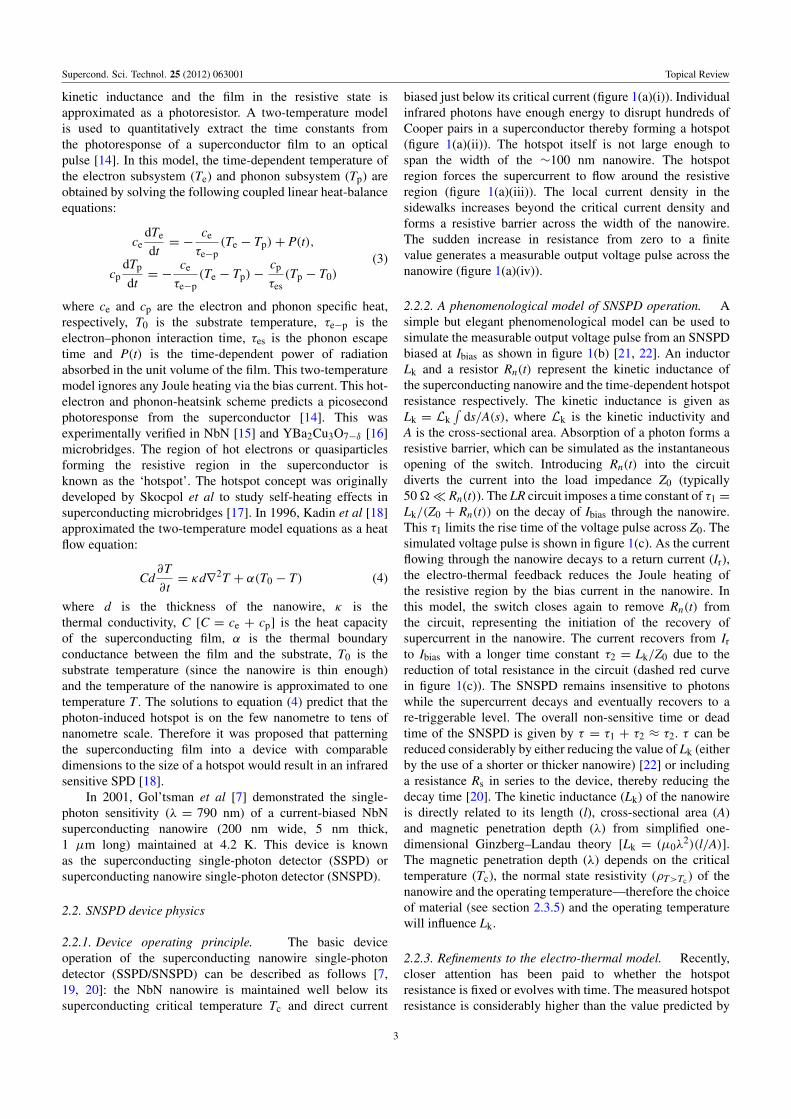
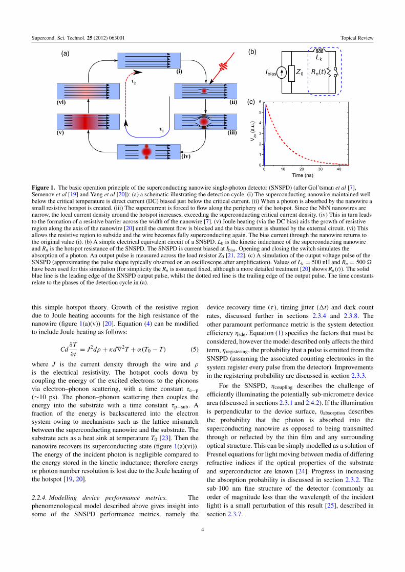
2.2.1. Device operating principle. The basic deviceoperation of the superconducting nanowire single-photondetector (SSPD/SNSPD) can be described as follows [7,19, 20]: the NbN nanowire is maintained well below itssuperconducting critical temperature Tc and direct current
biased just below its critical current (figure 1(a)(i)). Individualinfrared photons have enough energy to disrupt hundreds ofCooper pairs in a superconductor thereby forming a hotspot(figure 1(a)(ii)). The hotspot itself is not large enough tospan the width of the ∼100 nm nanowire. The hotspotregion forces the supercurrent to flow around the resistiveregion (figure 1(a)(iii)). The local current density in thesidewalks increases beyond the critical current density andforms a resistive barrier across the width of the nanowire.The sudden increase in resistance from zero to a finitevalue generates a measurable output voltage pulse across thenanowire (figure 1(a)(iv)).
2.2.2. A phenomenological model of SNSPD operation. Asimple but elegant phenomenological model can be used tosimulate the measurable output voltage pulse from an SNSPDbiased at Ibias as shown in figure 1(b) [21, 22]. An inductorLk and a resistor Rn(t) represent the kinetic inductance ofthe superconducting nanowire and the time-dependent hotspotresistance respectively. The kinetic inductance is given asLk = Lk
∫ds/A(s), where Lk is the kinetic inductivity and
A is the cross-sectional area. Absorption of a photon forms aresistive barrier, which can be simulated as the instantaneousopening of the switch. Introducing Rn(t) into the circuitdiverts the current into the load impedance Z0 (typically50�� Rn(t)). The LR circuit imposes a time constant of τ1 =
Lk/(Z0 + Rn(t)) on the decay of Ibias through the nanowire.This τ1 limits the rise time of the voltage pulse across Z0. Thesimulated voltage pulse is shown in figure 1(c). As the currentflowing through the nanowire decays to a return current (Ir),the electro-thermal feedback reduces the Joule heating ofthe resistive region by the bias current in the nanowire. Inthis model, the switch closes again to remove Rn(t) fromthe circuit, representing the initiation of the recovery ofsupercurrent in the nanowire. The current recovers from Irto Ibias with a longer time constant τ2 = Lk/Z0 due to thereduction of total resistance in the circuit (dashed red curvein figure 1(c)). The SNSPD remains insensitive to photonswhile the supercurrent decays and eventually recovers to are-triggerable level. The overall non-sensitive time or deadtime of the SNSPD is given by τ = τ1 + τ2 ≈ τ2. τ can bereduced considerably by either reducing the value of Lk (eitherby the use of a shorter or thicker nanowire) [22] or includinga resistance Rs in series to the device, thereby reducing thedecay time [20]. The kinetic inductance (Lk) of the nanowireis directly related to its length (l), cross-sectional area (A)and magnetic penetration depth (λ) from simplified one-dimensional Ginzberg–Landau theory [Lk = (µ0λ
2)(l/A)].The magnetic penetration depth (λ) depends on the criticaltemperature (Tc), the normal state resistivity (ρT>Tc ) of thenanowire and the operating temperature—therefore the choiceof material (see section 2.3.5) and the operating temperaturewill influence Lk.
2.2.3. Refinements to the electro-thermal model. Recently,closer attention has been paid to whether the hotspotresistance is fixed or evolves with time. The measured hotspotresistance is considerably higher than the value predicted by
3
Supercond. Sci. Technol. 25 (2012) 063001 Topical Review
(a) (b)
(c)
Figure 1. The basic operation principle of the superconducting nanowire single-photon detector (SNSPD) (after Gol’tsman et al [7],Semenov et al [19] and Yang et al [20]): (a) a schematic illustrating the detection cycle. (i) The superconducting nanowire maintained wellbelow the critical temperature is direct current (DC) biased just below the critical current. (ii) When a photon is absorbed by the nanowire asmall resistive hotspot is created. (iii) The supercurrent is forced to flow along the periphery of the hotspot. Since the NbN nanowires arenarrow, the local current density around the hotspot increases, exceeding the superconducting critical current density. (iv) This in turn leadsto the formation of a resistive barrier across the width of the nanowire [7]. (v) Joule heating (via the DC bias) aids the growth of resistiveregion along the axis of the nanowire [20] until the current flow is blocked and the bias current is shunted by the external circuit. (vi) Thisallows the resistive region to subside and the wire becomes fully superconducting again. The bias current through the nanowire returns tothe original value (i). (b) A simple electrical equivalent circuit of a SNSPD. Lk is the kinetic inductance of the superconducting nanowireand Rn is the hotspot resistance of the SNSPD. The SNSPD is current biased at Ibias. Opening and closing the switch simulates theabsorption of a photon. An output pulse is measured across the load resistor Z0 [21, 22]. (c) A simulation of the output voltage pulse of theSNSPD (approximating the pulse shape typically observed on an oscilloscope after amplification). Values of Lk = 500 nH and Rn = 500 �have been used for this simulation (for simplicity the Rn is assumed fixed, although a more detailed treatment [20] shows Rn(t)). The solidblue line is the leading edge of the SNSPD output pulse, whilst the dotted red line is the trailing edge of the output pulse. The time constantsrelate to the phases of the detection cycle in (a).
this simple hotspot theory. Growth of the resistive regiondue to Joule heating accounts for the high resistance of thenanowire (figure 1(a)(v)) [20]. Equation (4) can be modifiedto include Joule heating as follows:
Cd∂T
∂t= J2dρ + κd∇2T + α(T0 − T) (5)
where J is the current density through the wire and ρ
is the electrical resistivity. The hotspot cools down bycoupling the energy of the excited electrons to the phononsvia electron–phonon scattering, with a time constant τe−p(∼10 ps). The phonon–phonon scattering then couples theenergy into the substrate with a time constant τp−sub. Afraction of the energy is backscattered into the electronsystem owing to mechanisms such as the lattice mismatchbetween the superconducting nanowire and the substrate. Thesubstrate acts as a heat sink at temperature T0 [23]. Then thenanowire recovers its superconducting state (figure 1(a)(vi)).The energy of the incident photon is negligible compared tothe energy stored in the kinetic inductance; therefore energyor photon number resolution is lost due to the Joule heating ofthe hotspot [19, 20].
2.2.4. Modelling device performance metrics. Thephenomenological model described above gives insight intosome of the SNSPD performance metrics, namely the
device recovery time (τ ), timing jitter (1t) and dark countrates, discussed further in sections 2.3.4 and 2.3.8. Theother paramount performance metric is the system detectionefficiency ηsde. Equation (1) specifies the factors that must beconsidered, however the model described only affects the thirdterm, ηregistering, the probability that a pulse is emitted from theSNSPD (assuming the associated counting electronics in thesystem register every pulse from the detector). Improvementsin the registering probability are discussed in section 2.3.3.
For the SNSPD, ηcoupling describes the challenge ofefficiently illuminating the potentially sub-micrometre devicearea (discussed in sections 2.3.1 and 2.4.2). If the illuminationis perpendicular to the device surface, ηabsorption describesthe probability that the photon is absorbed into thesuperconducting nanowire as opposed to being transmittedthrough or reflected by the thin film and any surroundingoptical structure. This can be simply modelled as a solution ofFresnel equations for light moving between media of differingrefractive indices if the optical properties of the substrateand superconductor are known [24]. Progress in increasingthe absorption probability is discussed in section 2.3.2. Thesub-100 nm fine structure of the detector (commonly anorder of magnitude less than the wavelength of the incidentlight) is a small perturbation of this result [25], described insection 2.3.7.
4
Supercond. Sci. Technol. 25 (2012) 063001 Topical Review
(a)(b)
(c) (d)
(e)(f)
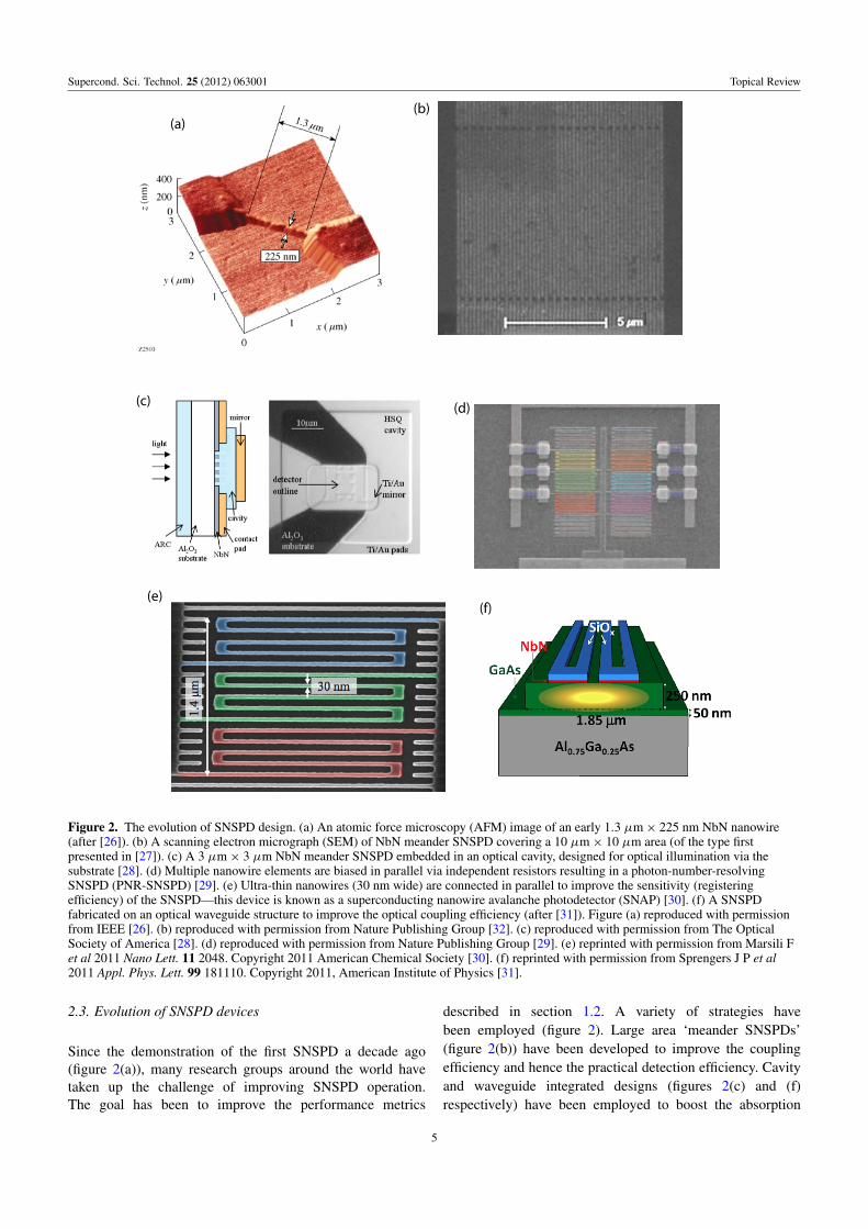
Figure 2. The evolution of SNSPD design. (a) An atomic force microscopy (AFM) image of an early 1.3 µm× 225 nm NbN nanowire(after [26]). (b) A scanning electron micrograph (SEM) of NbN meander SNSPD covering a 10 µm× 10 µm area (of the type firstpresented in [27]). (c) A 3 µm× 3 µm NbN meander SNSPD embedded in an optical cavity, designed for optical illumination via thesubstrate [28]. (d) Multiple nanowire elements are biased in parallel via independent resistors resulting in a photon-number-resolvingSNSPD (PNR-SNSPD) [29]. (e) Ultra-thin nanowires (30 nm wide) are connected in parallel to improve the sensitivity (registeringefficiency) of the SNSPD—this device is known as a superconducting nanowire avalanche photodetector (SNAP) [30]. (f) A SNSPDfabricated on an optical waveguide structure to improve the optical coupling efficiency (after [31]). Figure (a) reproduced with permissionfrom IEEE [26]. (b) reproduced with permission from Nature Publishing Group [32]. (c) reproduced with permission from The OpticalSociety of America [28]. (d) reproduced with permission from Nature Publishing Group [29]. (e) reprinted with permission from Marsili Fet al 2011 Nano Lett. 11 2048. Copyright 2011 American Chemical Society [30]. (f) reprinted with permission from Sprengers J P et al2011 Appl. Phys. Lett. 99 181110. Copyright 2011, American Institute of Physics [31].
2.3. Evolution of SNSPD devices
Since the demonstration of the first SNSPD a decade ago(figure 2(a)), many research groups around the world havetaken up the challenge of improving SNSPD operation.The goal has been to improve the performance metrics
described in section 1.2. A variety of strategies havebeen employed (figure 2). Large area ‘meander SNSPDs’(figure 2(b)) have been developed to improve the couplingefficiency and hence the practical detection efficiency. Cavityand waveguide integrated designs (figures 2(c) and (f)respectively) have been employed to boost the absorption
5
Supercond. Sci. Technol. 25 (2012) 063001 Topical Review
(a) (b)
(c) (d)
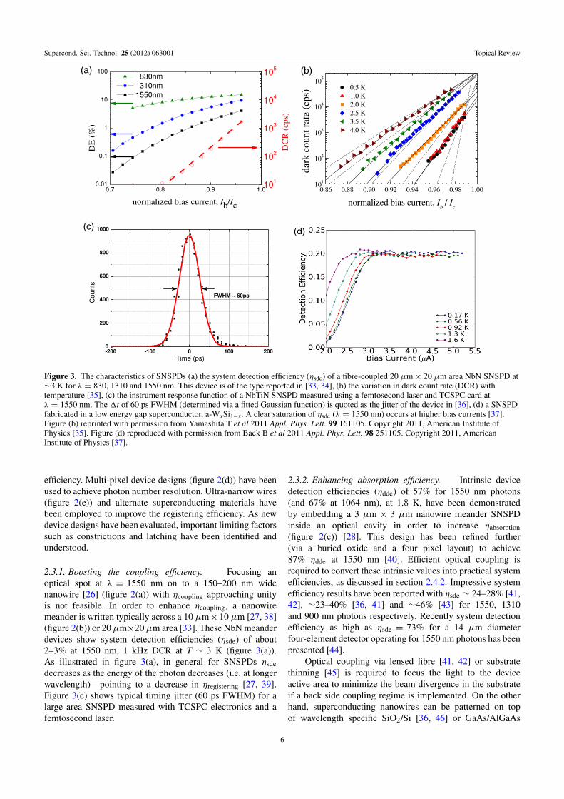
Figure 3. The characteristics of SNSPDs (a) the system detection efficiency (ηsde) of a fibre-coupled 20 µm× 20 µm area NbN SNSPD at∼3 K for λ = 830, 1310 and 1550 nm. This device is of the type reported in [33, 34], (b) the variation in dark count rate (DCR) withtemperature [35], (c) the instrument response function of a NbTiN SNSPD measured using a femtosecond laser and TCSPC card atλ = 1550 nm. The 1t of 60 ps FWHM (determined via a fitted Gaussian function) is quoted as the jitter of the device in [36], (d) a SNSPDfabricated in a low energy gap superconductor, a-WxSi1−x. A clear saturation of ηsde (λ = 1550 nm) occurs at higher bias currents [37].Figure (b) reprinted with permission from Yamashita T et al 2011 Appl. Phys. Lett. 99 161105. Copyright 2011, American Institute ofPhysics [35]. Figure (d) reproduced with permission from Baek B et al 2011 Appl. Phys. Lett. 98 251105. Copyright 2011, AmericanInstitute of Physics [37].
efficiency. Multi-pixel device designs (figure 2(d)) have beenused to achieve photon number resolution. Ultra-narrow wires(figure 2(e)) and alternate superconducting materials havebeen employed to improve the registering efficiency. As newdevice designs have been evaluated, important limiting factorssuch as constrictions and latching have been identified andunderstood.
2.3.1. Boosting the coupling efficiency. Focusing anoptical spot at λ = 1550 nm on to a 150–200 nm widenanowire [26] (figure 2(a)) with ηcoupling approaching unityis not feasible. In order to enhance ηcoupling, a nanowiremeander is written typically across a 10 µm×10 µm [27, 38](figure 2(b)) or 20µm×20µm area [33]. These NbN meanderdevices show system detection efficiencies (ηsde) of about2–3% at 1550 nm, 1 kHz DCR at T ∼ 3 K (figure 3(a)).As illustrated in figure 3(a), in general for SNSPDs ηsdedecreases as the energy of the photon decreases (i.e. at longerwavelength)—pointing to a decrease in ηregistering [27, 39].Figure 3(c) shows typical timing jitter (60 ps FWHM) for alarge area SNSPD measured with TCSPC electronics and afemtosecond laser.
2.3.2. Enhancing absorption efficiency. Intrinsic devicedetection efficiencies (ηdde) of 57% for 1550 nm photons(and 67% at 1064 nm), at 1.8 K, have been demonstratedby embedding a 3 µm × 3 µm nanowire meander SNSPDinside an optical cavity in order to increase ηabsorption(figure 2(c)) [28]. This design has been refined further(via a buried oxide and a four pixel layout) to achieve87% ηdde at 1550 nm [40]. Efficient optical coupling isrequired to convert these intrinsic values into practical systemefficiencies, as discussed in section 2.4.2. Impressive systemefficiency results have been reported with ηsde ∼ 24–28% [41,42], ∼23–40% [36, 41] and ∼46% [43] for 1550, 1310and 900 nm photons respectively. Recently system detectionefficiency as high as ηsde = 73% for a 14 µm diameterfour-element detector operating for 1550 nm photons has beenpresented [44].
Optical coupling via lensed fibre [41, 42] or substratethinning [45] is required to focus the light to the deviceactive area to minimize the beam divergence in the substrateif a back side coupling regime is implemented. On the otherhand, superconducting nanowires can be patterned on topof wavelength specific SiO2/Si [36, 46] or GaAs/AlGaAs
6
Supercond. Sci. Technol. 25 (2012) 063001 Topical Review
distributed Bragg mirrors [47]. The advantage here is thatfront side fibre coupling is sufficient to enhance absorptionfor these devices. The coupling can be further improved byintegrating an Au optical antenna with the nanowires [48].
Recently several groups have proposed [49, 50] ordemonstrated [31, 51–53] embedding the nanowire in anoptical waveguide [31, 49–53] (an example is illustrated infigure 2(f)). A nanowire running along the length of an opticalwaveguide [31, 52] should give a long interaction lengthfor incident photons, allowing ηabsorption to be maximized.An array of nanowires can be used to sample a standingwave in an optical waveguide interferometer for spectroscopyapplications [51, 53].
2.3.3. Improving registering efficiency. ηregistering of thedevice can be improved by reducing the width of thenanowires. Multiple narrow wires can be placed in parallelto boost the output signal whilst improving long wavelengthsensitivity [54]. Ultra-narrow nanowire (20 or 30 nm)devices (figure 2(e)) have been demonstrated to be moreresponsive to low energy photons than typical nanowiredevices (90 nm) [30]. In this work four ultra-narrow nanowireelements are placed in parallel, and the device is referredto as a superconducting nanowire avalanche photodetector(SNAP). Maximum ηregistering is observed as ηdde saturates ata lower bias current. Upon absorption of a photon in a singleparallel element of the device, the element turns resistive anddiverts additional current into the other elements, switchingthe entire device resistive by exceeding the critical current ofthe parallel elements [55]. If the bias current is significantlylower than the critical current, the first photon absorptionswitches the first element but the diverted current may not beenough to trigger the avalanche. In this scenario, the devicewaits either for a second photon to be absorbed in anotherelement or the occurrence of a dark count in another elementto switch the whole device resistive. If this does not occurthe device can recover without completing the avalanche andregistering a count [55]. The registering probability saturationis also observed when smaller superconducting gap energymaterials such as a-WxSi1−x [37] (figure 3(d)) are used forfabrication of SNSPDs. These devices exhibit ηdde saturation(and near-unity ηregistering) at λ = 1550 nm even when thenanowires are 150 nm wide with 4.5 nm film thickness. Thisbehaviour is most likely a consequence of the smaller sizeof superconducting energy gap in this material leading to anincreased hotspot size for a given photon energy.
2.3.4. Constrictions, latching and recovery time. Fabricatinguniform, large area meanders [27, 33, 38, 56] or meanderswith fill factors >50% [57] with high yield remains achallenge. Constrictions in the nanowire do not allow thedetector to be biased at a high current, consequently loweringηdde of the device due to a lower ηregistering [58]. Nano-opticalstudies have been undertaken to confirm that a constricteddevice is sensitive only at the constriction and is insensitiveor less sensitive at the non-constricted regions due to lowercurrent density [59]. For a given defect density, reducingthe area of nanowire meander will improve the nanowire
uniformity. 3 µm × 3 µm devices have been shown to behighly uniform exhibiting higher ηdde [58]. However, couplingthe light efficiently to this small 3 µm × 3 µm area ischallenging. Lk is lower for shorter nanowires, resulting ina shorter τ . This makes shorter nanowires highly suitablefor high speed applications. The load impedance can alsobe increased to reduce τ . However, τ suppression has alimitation. If τ is reduced excessively, the current willreturn to the nanowire too rapidly. Joule heating results ina self-heating hotspot [60]. This self-heating hotspot causesthe nanowire to enter into a ‘latched’ state, preventingfurther detection of photons without manually reducing Ibias.Alternatively, the inductance of the detector can be reducedby writing a set of parallel nanowires [61–63] or an array ofparallel nanowire pixels [64] rather than relying on a singlemeander nanowire across a given area.
2.3.5. Alternate superconducting materials for SNSPDs.NbN was the first choice material for SNSPDs. SubsequentlySNSPDs have also been demonstrated using NbTiN (asuperconducting material with very similar properties to NbN)on silicon-based substrates [65, 66]. NbTiN nanowire deviceshave been shown to possess low Lk due to their low resistivityabove the superconducting transition temperature, thereforeNbTiN SNSPDs have smaller τ compared to the NbNdevices [66]. Similarly Nb SNSPDs have lower resistivitythan NbN resulting in shorter τ , but the Nb devices sufferfrom latching due to their slow energy relaxation process [67].Fabricating a superconducting nanowire meander using novelor high-Tc superconductors is arguably just a questionof technological development. Recently MgB2 SNSPDshave been fabricated [68] and single-photon sensitivityat visible wavelengths has been demonstrated [69], butnew fabrication and film growth techniques have to bedeveloped to increase the active area by patterning uniformmeanders without defects. Ultra-thin nanowires have beenprocessed in YBa2Cu3O7−δ thin films but single-photonsensitivity is yet to be demonstrated at visible or infraredwavelengths [70]. Fabrication challenges aside, this resultmay be expected as high-Tc superconducting materials have alarge superconducting gap energy compared to NbN, reducingthe sensitivity to photons of a given energy. Single-photonsensitivity has been reported in NbN SNSPDs up to 5 µmwavelength, albeit with a significant reduction in ηdde (andηregistering) as wavelength increases [39]. SNSPDs basedon smaller superconducting gap energy materials such asamorphous WxSi1−x [37] (see section 2.3.3 and figure 3(d)),NbSi [71] and TaN [72] appear to have better sensitivitythan NbN at longer wavelengths. These low energy gapsuperconducting materials have lower transition temperatures,so the SNSPD operating temperature is reduced (requiringmore advanced cooling techniques than those discussed insection 2.4.1).
2.3.6. Resolving multi-photon events. Multi-elementSNSPDs (MESNSPDs) offer another solution to improvingthe single-photon count rate and achieving photon numberresolution (PNR) [64, 73]. MESNSPDs consist of spatially
7
Supercond. Sci. Technol. 25 (2012) 063001 Topical Review
interleaved nanowires meandering across a large active area.In this configuration each element is independently currentbiased and requires an individual readout [64]. This designreduces the dead time without compromising on Lk or Z0,with no apparent cross-talk between pixels. When the pixelsof the MESNSPDs are broadly illuminated photon numberresolution can be achieved [73].
An alternative approach to achieving PNR in SNSPDsis by connecting multiple nanowire elements in parallel,provided the hotspot creation in one element does notaffect the superconducting state of the remaining elements.This is achieved by current biasing each nanowire elementindependently with a single voltage source, by introducinga tailored series resistance in each nanowire element [29](figure 2(d)). The resistance values are carefully chosen suchthat the hotspot formation diverts the current into Z0 insteadof flowing into the remaining nanowires. When ‘n’ individualelements fire simultaneously, current flowing into Z0 increasesby a factor of ‘n’. This PNR-SNSPD output results in a‘n’ times taller observable voltage pulse providing PNRcapability [29, 74].
Another technique to observe multi-photon eventsusing SNSPDs is to reduce the bias current and rely onthe absorption of multiple photons to form a resistivebarrier across the nanowire [7, 75]. Recently new detectortomography techniques have been employed to examine thisregime [76]. However, at low current bias the SNSPD istypically much less efficient, so this multi-photon detectionregime is hard to exploit in practical applications.
2.3.7. Polarization dependence in SNSPDs. From anoptical standpoint, the meander SNSPD device is essentiallya subwavelength grating and is observed to possess noticeablepolarization sensitivity that varies with wavelength [25].The count rate from the detector (and hence ηsde) displaysa maximum and a minimum value depending on whetherthe electric field is either parallel or perpendicular tothe nanowire. This polarization dependent variation inηabsorption due to the meander structure can be simulatedconvincingly [25]. This effect can be mitigated by usingspiral and perpendicular device designs [77]. These designseliminate the SNSPD polarization sensitivity by accepting anintermediate efficiency.
2.3.8. Noise mechanisms in SNSPDs: dark counts and timingjitter. The signal-to-noise ratio, which can be achievedwith an SNSPD, is governed not just by the practicalefficiency (ηsde) and the dark count rate (DCR) but alsotiming jitter (1t) [10]. The DCR of the SNSPD is a crucialfactor in the device performance. Empirically, the DCR raterises exponentially as Ibias approaches Ic (figure 3(a)) [33].It is clear from these data (from a device with a largearea meander with no cavity) at the shorter illuminationwavelength (λ = 830 nm) relatively high efficiency canbe achieved at negligible dark count rates. The origin ofthe exponential behaviour of dark count rate with bias ispoorly understood. Theoretical explanations centre on thepossible transit of flux vortices across the current-carrying
superconducting nanowire. Several mechanisms have beenput forward: quantum phase-slips, single-vortex crossings andvortex–antivortex pair nucleation [78].
Experimental tests have been far from conclusive [79,80], owing to the difficulty of differentiating these fundamen-tal mechanisms from prosaic environmental noise owing tothe bias and readout configuration. Recent studies of darkcounts over a wide temperature range (0.5–4 K) providevaluable fresh data [35] (see figure 3(b)). Furthermore, newtheoretical studies also indicate that the device geometry (inparticular, tight bends in the meander structure) may play acrucial role in triggering dark counts [81].
The very low timing jitter 1t of SNSPDs makes thesedetectors very attractive for TCSPC applications. Whenthe arrival time of the photon is known extremely well(using modern ultrafast optical sources) the main timinguncertainty arises from the jitter of the SPD. The lowesttiming jitter reported is 18 ps [82], but this result has notbeen widely reproduced and the dimensions of the deviceused and photon flux were unclear. 29 ps FWHM has beendemonstrated in small area (4 µm × 4.2 µm) single- andmulti-pixel SNSPDs [73]. Larger area SNSPDs typically givelarger timing jitter when measured with femtosecond lasersources and state-of-the-art TCSPC electronics: for example10 µm × 10 µm meanders of the type first reported byVerevkin [27] give 68 ps FWHM [83] and 20 µm × 20 µmmeander devices [33] give 60 ps FWHM (figure 3(c)). Theseresults indicate that a highly uniform nanowire (most easilyachieved with a short wire length) will give lower timingjitter. Higher critical currents have been observed to improvejitter in uniform devices [84] allowing 40 ps FWHM to bedemonstrated in 15 µm × 15 µm meander devices [85].Recently studies using nano-optical techniques to studythe local efficiency and timing properties of SNSPDs [86]indicate that different parts of a non-uniform nanowire givedifferent hotspot resistances yielding different pulse risetimes, broadening the overall timing jitter.
2.4. Practical considerations: cooling, optical coupling anddevice readout
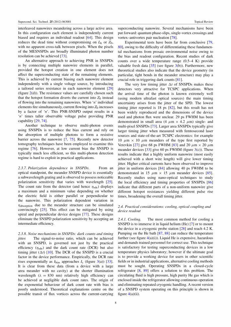
2.4.1. Cooling. The most common method for cooling aSNSPD is to immerse it in liquid helium (He) [7] or to mountthe device in a cryogenic probe station [28] and reach 4.2 K.Pumping on the He bath [87, 88] can reduce the temperaturefurther (see figure 4(a)(i)). Liquid He is expensive, hazardousand demands trained personnel for correct use. This techniqueis satisfactory for testing superconducting devices in a lowtemperature physics laboratory; however if the ultimate goalis to provide a working device for users in other scientificfields or in industrial applications, alternative cooling methodsmust be sought. Operating SNSPDs in a closed-cyclerefrigerator [8, 89] offers a solution to this problem. Thecirculating fluid is high pressure, high purity He gas which isenclosed inside the refrigerator allowing continuous operationand eliminating repeated cryogenic handling. A recent versionof a SNSPD system operating on this principle is shown infigure 4(a)(ii).
8
Supercond. Sci. Technol. 25 (2012) 063001 Topical Review
Figure 4. (a) Cooling techniques for SNSPDs (i) liquid helium dewar [88] (ii) Gifford–McMahon (GM) closed-cycle refrigerator.(b) Optical coupling techniques (i) fibre coupling (as used in [34, 36]) (ii) GRIN lens fibre coupling [41] and (iii) confocal microscopy setupin a GM cryocooler (as used in [86]). Figure (a)(i) reproduced with permission from IEEE [88], (b)(ii) reproduced with permission fromThe Optical Society of America [41].
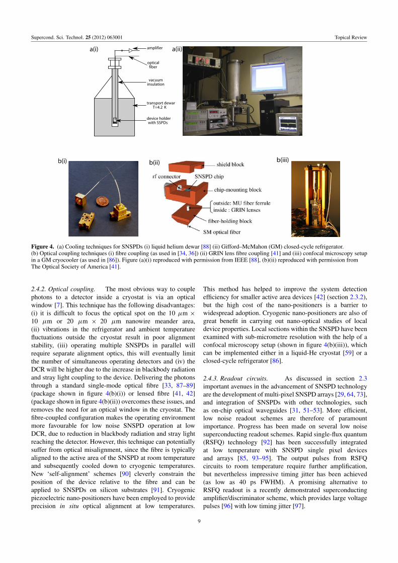
2.4.2. Optical coupling. The most obvious way to couplephotons to a detector inside a cryostat is via an opticalwindow [7]. This technique has the following disadvantages:(i) it is difficult to focus the optical spot on the 10 µm ×10 µm or 20 µm × 20 µm nanowire meander area,(ii) vibrations in the refrigerator and ambient temperaturefluctuations outside the cryostat result in poor alignmentstability, (iii) operating multiple SNSPDs in parallel willrequire separate alignment optics, this will eventually limitthe number of simultaneous operating detectors and (iv) theDCR will be higher due to the increase in blackbody radiationand stray light coupling to the device. Delivering the photonsthrough a standard single-mode optical fibre [33, 87–89](package shown in figure 4(b)(i)) or lensed fibre [41, 42](package shown in figure 4(b)(ii)) overcomes these issues, andremoves the need for an optical window in the cryostat. Thefibre-coupled configuration makes the operating environmentmore favourable for low noise SNSPD operation at lowDCR, due to reduction in blackbody radiation and stray lightreaching the detector. However, this technique can potentiallysuffer from optical misalignment, since the fibre is typicallyaligned to the active area of the SNSPD at room temperatureand subsequently cooled down to cryogenic temperatures.New ‘self-alignment’ schemes [90] cleverly constrain theposition of the device relative to the fibre and can beapplied to SNSPDs on silicon substrates [91]. Cryogenicpiezoelectric nano-positioners have been employed to provideprecision in situ optical alignment at low temperatures.
This method has helped to improve the system detectionefficiency for smaller active area devices [42] (section 2.3.2),but the high cost of the nano-positioners is a barrier towidespread adoption. Cryogenic nano-positioners are also ofgreat benefit in carrying out nano-optical studies of localdevice properties. Local sections within the SNSPD have beenexamined with sub-micrometre resolution with the help of aconfocal microscopy setup (shown in figure 4(b)(iii)), whichcan be implemented either in a liquid-He cryostat [59] or aclosed-cycle refrigerator [86].
2.4.3. Readout circuits. As discussed in section 2.3important avenues in the advancement of SNSPD technologyare the development of multi-pixel SNSPD arrays [29, 64, 73],and integration of SNSPDs with other technologies, suchas on-chip optical waveguides [31, 51–53]. More efficient,low noise readout schemes are therefore of paramountimportance. Progress has been made on several low noisesuperconducting readout schemes. Rapid single-flux quantum(RSFQ) technology [92] has been successfully integratedat low temperature with SNSPD single pixel devicesand arrays [85, 93–95]. The output pulses from RSFQcircuits to room temperature require further amplification,but nevertheless impressive timing jitter has been achieved(as low as 40 ps FWHM). A promising alternative toRSFQ readout is a recently demonstrated superconductingamplifier/discriminator scheme, which provides large voltagepulses [96] with low timing jitter [97].
9
Supercond. Sci. Technol. 25 (2012) 063001 Topical Review
3. Advanced photon-counting applications withSNSPDs
3.1. Overview
SNSPDs are highly promising alternatives for time-correlatedsingle-photon counting (TCSPC) [9] at infrared wavelengths,offering single-photon sensitivity combined with low DCR,low 1t, short recovery times and free-running operation.Detailed comparisons have been made between SNSPDs,SPADs and other photon-counting technologies in [10,table 1] and [98, table II]. Over the past decade, theburgeoning field of optical quantum information science(QIS) has acted as a powerful driver for infrared single-photondetector development [99]. SNSPDs now play a significantrole as an enabling technology in the QIS arena [10].These experiments rely on the detection of coincidencesbetween correlated photons; the detection rate of two-foldcoincidences will scale as (ηsde)
2, and the detection rate ofan n-fold coincidence will scale as (ηsde)
n, so as SNSPDtechnology improves, much more challenging experimentsbecome feasible. However, it is important to appreciate thatthe scope of potential applications for SNSPDs is much widerthan QIS: SNSPD technology is potentially an alternative forany current application of the InGaAs SPAD [12], the mostwidely available commercial alternative for photon countingin the 1–1.7 µm wavelength range. In this concluding sectionof our review, we survey the use of SNSPDs in severalimportant application areas: quantum key distribution (QKD),optical quantum computing, characterization of quantumemitters, space-to-ground communications, integrated circuittesting, fibre sensing and time-of-flight ranging.
3.2. Quantum key distribution (QKD)
Quantum key distribution [100] (also referred to as quantumcryptography) is a method for two parties (known asAlice & Bob) to create a cryptographic key via a publiccommunications channel. This is achieved in practice byencoding information on the phase or polarization of singlephotons. Any attempt by an eavesdropper (Eve) to interceptand duplicate the key will be revealed by an elevatederror rate. A variety of QKD protocols and practicalimplementations now exist. The ideal wavelength for longdistance transmission in optical fibre is 1550 nm. Thereforefor long distance QKD in optical fibre, high performancesingle-photon detectors at λ = 1550 nm are essential. A lowDCR is highly desirable, as dark counts contribute to the errorrate. Low 1t allows photon arrivals to be time-stamped veryprecisely. High ηsde is desirable, but not essential as significantlosses occur elsewhere (e.g. in the fibre link and in the receiveroptics).
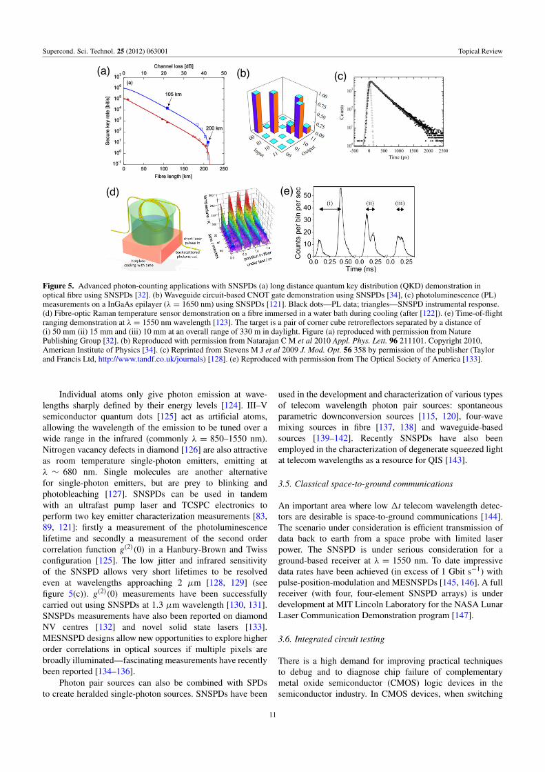
The first proof-of-principle demonstration using SNSPDsin QKD was carried out by the NIST and BBN groups [101].A high bit rate, short wavelength (λ = 850 nm) demonstrationwas then reported [102]. However, the undoubted break-through result was a high bit rate long distance demonstrationat λ = 1550 nm carried out at Stanford University [32]
(figure 5(a)). This demonstration exceeded 200 km trans-mission range for the first time, and record bit rates wereachieved at shorter distances—a significant improvement onthe best QKD results achieved at that time with InGaAsSPADs [103]. Since that study, further QKD demonstrationshave been reported using SNSPDs: the maximum rangehas been extended to 250 km (using low loss fibre) [104],novel decoy state protocols have been demonstrated [105,106], entanglement-based QKD has been demonstrated overlong distance [107], SNSPDs have been implemented inQKD field trials in installed fibre networks [108–110] andhigh key transmission rates have been demonstrated [111].Attention has turned to detector-based security loopholes inQKD—recent work [112] suggests that SNSPDs may besusceptible to ‘quantum hacking’ if care is not taken in theinstallation of the detectors in a QKD system.
3.3. Development of optical quantum computing
The realization of a quantum computer [113] is undoubtedlyone of the grand challenges for physics in the 21st century,and is the focus of considerable efforts in the QIS community.The template for a scalable optical quantum computerwas set out in 2001 [114]. This scheme places stringentrequirements on single-photon detector technology, namelydetectors with near-unity ηsde and PNR capability [10]. As theperformance of SNSPDs has steadily improved, SNSPDs havebegun to be used in proof-of-principle QIS demonstrations,relying on the detection of multi-photon coincidences. Theuse of a low ηsde SNSPD in tandem with a higher ηsdeInGaAs SPAD [115], allowed high coincidence rates tobe obtained at telecom wavelengths in these challengingexperiments. Key demonstrations employing SNSPDs in thisway include the demonstration of the first telecom wavelengthcontrolled-NOT gate (the basic building block of a quantumcomputer) [116], long distance entanglement swapping [117]and quantum storage of entanglement [118]. Another notabledevelopment in optical QIS has been the adoption ofon-chip optical waveguides to replace bulk optics in quantumwaveguide circuits [119]. Proof-of-principle demonstrationshave been carried out using SNSPDs in conjunction with firstgeneration quantum waveguide circuits at λ = 804 nm [34](see figure 5(b)). The true benefit is seen however at λ =1550 nm, where much higher performance reconfigurablewaveguide circuits can be employed for the first time usingSNSPDs [120]. The integration of SNSPDs with waveguides(discussed in section 2.3.2 [31, 52]) will allow these two QIStechnologies to be combined on-chip.
3.4. Characterization of quantum emitters
Single-photon emission from atoms, quantum dots andmolecules can be harnessed as a tool for production ofquantum states of light for QIS and as a powerful monitoringtechnique in the life sciences. Considerable efforts are alsounderway to develop sources of correlated or entangledphotons for QIS applications. SNSPDs are a powerfulenabling tool for these studies at infrared wavelengths.
10
Supercond. Sci. Technol. 25 (2012) 063001 Topical Review
(a) (c)
(d) (e)
(b)
Figure 5. Advanced photon-counting applications with SNSPDs (a) long distance quantum key distribution (QKD) demonstration inoptical fibre using SNSPDs [32]. (b) Waveguide circuit-based CNOT gate demonstration using SNSPDs [34], (c) photoluminescence (PL)measurements on a InGaAs epilayer (λ = 1650 nm) using SNSPDs [121]. Black dots—PL data; triangles—SNSPD instrumental response.(d) Fibre-optic Raman temperature sensor demonstration on a fibre immersed in a water bath during cooling (after [122]). (e) Time-of-flightranging demonstration at λ = 1550 nm wavelength [123]. The target is a pair of corner cube retroreflectors separated by a distance of(i) 50 mm (ii) 15 mm and (iii) 10 mm at an overall range of 330 m in daylight. Figure (a) reproduced with permission from NaturePublishing Group [32]. (b) Reproduced with permission from Natarajan C M et al 2010 Appl. Phys. Lett. 96 211101. Copyright 2010,American Institute of Physics [34]. (c) Reprinted from Stevens M J et al 2009 J. Mod. Opt. 56 358 by permission of the publisher (Taylorand Francis Ltd, http://www.tandf.co.uk/journals) [128]. (e) Reproduced with permission from The Optical Society of America [133].
Individual atoms only give photon emission at wave-lengths sharply defined by their energy levels [124]. III–Vsemiconductor quantum dots [125] act as artificial atoms,allowing the wavelength of the emission to be tuned over awide range in the infrared (commonly λ = 850–1550 nm).Nitrogen vacancy defects in diamond [126] are also attractiveas room temperature single-photon emitters, emitting atλ ∼ 680 nm. Single molecules are another alternativefor single-photon emitters, but are prey to blinking andphotobleaching [127]. SNSPDs can be used in tandemwith an ultrafast pump laser and TCSPC electronics toperform two key emitter characterization measurements [83,89, 121]: firstly a measurement of the photoluminescencelifetime and secondly a measurement of the second ordercorrelation function g(2)(0) in a Hanbury-Brown and Twissconfiguration [125]. The low jitter and infrared sensitivityof the SNSPD allows very short lifetimes to be resolvedeven at wavelengths approaching 2 µm [128, 129] (seefigure 5(c)). g(2)(0) measurements have been successfullycarried out using SNSPDs at 1.3 µm wavelength [130, 131].SNSPDs measurements have also been reported on diamondNV centres [132] and novel solid state lasers [133].MESNSPD designs allow new opportunities to explore higherorder correlations in optical sources if multiple pixels arebroadly illuminated—fascinating measurements have recentlybeen reported [134–136].
Photon pair sources can also be combined with SPDsto create heralded single-photon sources. SNSPDs have been
used in the development and characterization of various typesof telecom wavelength photon pair sources: spontaneousparametric downconversion sources [115, 120], four-wavemixing sources in fibre [137, 138] and waveguide-basedsources [139–142]. Recently SNSPDs have also beenemployed in the characterization of degenerate squeezed lightat telecom wavelengths as a resource for QIS [143].
3.5. Classical space-to-ground communications
An important area where low 1t telecom wavelength detec-tors are desirable is space-to-ground communications [144].The scenario under consideration is efficient transmission ofdata back to earth from a space probe with limited laserpower. The SNSPD is under serious consideration for aground-based receiver at λ = 1550 nm. To date impressivedata rates have been achieved (in excess of 1 Gbit s−1) withpulse-position-modulation and MESNSPDs [145, 146]. A fullreceiver (with four, four-element SNSPD arrays) is underdevelopment at MIT Lincoln Laboratory for the NASA LunarLaser Communication Demonstration program [147].
3.6. Integrated circuit testing
There is a high demand for improving practical techniquesto debug and to diagnose chip failure of complementarymetal oxide semiconductor (CMOS) logic devices in thesemiconductor industry. In CMOS devices, when switching
11
Supercond. Sci. Technol. 25 (2012) 063001 Topical Review
takes place, field effect transistors (FETs) in the saturationmode develop a high field (∼105 V cm−1) in the pinch offregion of the conduction channel, driving electrons to highenergy (>1 eV). Photon emission takes place as the electronslose energy. As the transistor size decreases, the gate sizedecreases, reducing the required bias voltage and resulting inlonger wavelength emissions. Emitted photons are typicallyin the NIR region. The detection of these single photonsusing SNSPDs enables the semiconductor industry to analysethe timing parameters of the CMOS device, and a prototypeSNSPD circuit testing system has been reported [148, 149].
3.7. Fibre temperature sensing
With telecom wavelength single-photon sensitivity, lowDCRs, low 1t and free-running operation; SNSPDs offernew opportunities in fibre sensing applications. An opticalpulse passing through optical fibre is scattered to wavelengthsabove and below the pump wavelength via Raman scattering.SNSPDs are capable of detecting this faint backscatteredsignal in single-mode telecom fibre. By comparing the ratioof these Raman signals (known as the Stokes and anti-Stokesbands) it is possible to extract the temperature. With theadditional timing information provided by the pump pulse andthe low jitter SNSPD (coupled with TCSPC) it is possible toextract temperature as a function of length along the fibre.Initial studies [122, 150] (figure 5(d)) show that a spatialresolution of ∼1 cm and a temperature uncertainty of 3 Kcan be achieved with integration times as short as 60 s in atest fibre ∼1 m in length. With increased pump power, muchshorter integration times and overall range could be achieved.Optical fibres are routinely installed in large-scale structures(buildings, pipelines)—the beauty of a fibre sensing system isthat a new sensor can simply be plugged into the existing fibreinfrastructure.
3.8. Time-of-flight depth ranging
TCSPC can be used to improve the range and performanceof light detection and ranging (LIDAR) systems [151].The basic principle is as follows—a short laser pulse istransmitted and the reflected signal from a distant targetis collected and routed to a single-photon detector. With afew picosecond pulsed laser, a low 1t detector and TCPSCelectronics, very good depth resolution can be achieved.SNSPDs offer an important advantage over Si SPAD detectorsin this application—operation at telecom wavelengths withthe SNPSDs allow solar background to be reduced and thiswavelength is considered eye safe. Depth ranging studieshave been carried out with SNSPDs at λ = 1550 nm,achieving a depth resolution of 1 cm at 330 m range indaylight (ηsde 1%, 1t 70 ps FHWM) [123] (figure 5(e)).In the future, scanning optics can be added to the systemto achieve depth imaging [152] with similar performance.Improvements in laser power and ηsde will allow acceleratedimaging speeds or greater range. A very long distance (∼4×10⁸ m) time-of-flight experiment will be performed as partof the Lunar Laser Communication Demonstration using
SNSPDs [147] (see section 3.5). Improving 1t will allowbetter depth resolution. Moreover there is potential to useSNSPD in a wider range of atmospheric sensing applications(e.g. sensing of greenhouse gases via DIAL—differentialabsorption LIDAR [153]).
4. Conclusion
Over the past decade superconducting nanowire single-photondetector (SNSPD) technology has advanced apace. Thebasic device performance has improved dramatically, offeringhigh ηsde, low DCR and low 1t at infrared wavelengths,outperforming the best available semiconductor-based single-photon detectors. Improvements in cooling technologyhave aided the adoption of SNSPDs in a wide rangeof applications. As this review illustrates, high impactphoton-counting demonstrations using SNSPDs have beencarried out in diverse fields, from quantum informationscience to atmospheric time-of-flight ranging. There is noquestion that over the coming decade SNSPDs will have animportant role to play in many further scientific advances andapplications.
Acknowledgments
The authors thank colleagues who provided figures andfeedback on this paper. The authors thank the UK Engineeringand Physical Sciences Research Council (EPSRC) forsupport. CMN acknowledges a SU2P EntrepreneurialFellowship and RHH acknowledges a Royal SocietyUniversity Research Fellowship.
References
[1] Onnes H K 1911 The resistance of pure mercury at heliumtemperatures Commun. Phys. Lab. Univ. Leiden120b 1479–81
[2] Testardi L R 1971 Destruction of superconductivity by laserlight Phys. Rev. B 4 2189–96
[3] Richards P L 1994 Bolometers for infrared and millimeterwaves J. Appl. Phys. 76 1–24
[4] Peacock A et al 1996 Single optical photon detection with asuperconducting tunnel junction Nature 381 135–7
[5] Irwin K D 1995 An application of electrothermal feedbackfor high-resolution cryogenic particle-detection Appl.Phys. Lett. 66 1998–2000
[6] Day P K, LeDuc H G, Mazin B A, Vayonakis A andZmuidzinas J 2003 A broadband superconducting detectorsuitable for use in large arrays Nature 425 817–21
[7] Gol’tsman G N, Okunev O, Chulkova G, Lipatov A,Semenov A, Smirnov K, Voronov B, Dzardanov A,Williams C and Sobolewski R 2001 Picosecondsuperconducting single-photon optical detector Appl.Phys. Lett. 79 705–7
[8] Radebaugh R 2004 Refrigeration for superconductors Proc.IEEE 92 1719–34
[9] Becker W 2005 Advanced Time-Correlated Single PhotonCounting Techniques (Springer Ser. Chemical Physics vol81)
[10] Hadfield R H 2009 Single-photon detectors for opticalquantum information applications Nature Photon.3 696–705
12
Supercond. Sci. Technol. 25 (2012) 063001 Topical Review
[11] Cova S, Ghioni M, Lotito A, Rech I and Zappa F 2004Evolution and prospects for single-photon avalanchediodes and quenching circuits J. Mod. Optic. 51 1267–88
[12] Itzler M A, Jiang X D, Entwistle M, Slomkowski K, Tosi A,Acerbi F, Zappa F and Cova S 2011 Advances inInGaAsP-based avalanche diode single photon detectorsJ. Mod. Opt. 58 174–200
[13] Bluzer N 1992 Temporal relaxation measurements ofphotoinduced nonequilibrium in superconductors J. Appl.Phys. 71 1336–48
[14] Semenov A D, Nebosis R S, Gousev Y P,Heusinger M A and Renk K F 1995 Analysis of thenonequilibrium photoresponse of superconducting films topulsed radiation by use of a two-temperature model Phys.Rev. B 52 581–90
[15] Lindgren M, Currie M, Zeng W S, Sobolewski R,Cherednichenko S, Voronov B and Gol’tsman G N 1998Picosecond response of a superconducting hot-electronNbN photodetector Appl. Supercond. 6 423–8
[16] Lindgren M, Currie M, Williams C, Hsiang T Y,Fauchet P M, Sobolewski R, Moffat S H, Hughes R A,Preston J S and Hegmann F A 1999 Intrinsic picosecondresponse times of Y–Ba–Cu–O superconductingphotodetectors Appl. Phys. Lett. 74 853–5
[17] Skocpol W J, Beasley M R and Tinkham M 1974Self-heating hotspots in superconducting thin-filmmicrobridges J. Appl. Phys. 45 4054–66
[18] Kadin A M and Johnson M W 1996 Nonequilibriumphoton-induced hotspot: a new mechanism forphotodetection in ultrathin metallic films Appl. Phys. Lett.69 3938–40
[19] Semenov A D, Gol’tsman G N and Korneev A A 2001Quantum detection by current carrying superconductingfilm Physica C 351 349–56
[20] Yang J K W, Kerman A J, Dauler E A, Anant V,Rosfjord K M and Berggren K K 2007 Modeling theelectrical and thermal response of superconductingnanowire single-photon detectors IEEE Trans. Appl.Supercond. 17 581–5
[21] Hadfield R H, Miller A J, Nam S W, Kautz R L andSchwall R E 2005 Low-frequency phase locking inhigh-inductance superconducting nanowires Appl. Phys.Lett. 87 203505
[22] Kerman A J, Dauler E A, Keicher W E, Yang J K W,Berggren K K, Gol’tsman G and Voronov B 2006Kinetic-inductance-limited reset time of superconductingnanowire photon counters Appl. Phys. Lett. 88 111116
[23] Il’in K S, Lindgren M, Currie M, Semenov A D,Gol’tsman G N, Sobolewski R, Cherednichenko S I andGershenzon E M 2000 Picosecond hot-electron energyrelaxation in NbN superconducting photodetectors Appl.Phys. Lett. 76 2752–4
[24] Macleod H A 2010 Thin-film Optical Filters 4th edn (BocaRaton, FL: Taylor and Francis/CRC Press)
[25] Anant V, Kerman A J, Dauler E A, Yang J K W,Rosfjord K M and Berggren K K 2008 Optical propertiesof superconducting nanowire single-photon detectors Opt.Express 16 10750–61
[26] Gol’tsman G, Okunev O, Chulkova G, Lipatov A,Dzardanov A, Smirnov K, Semenov A, Voronov B,Williams C and Sobolewski R 2001 Fabrication andproperties of an ultrafast NbN hot-electron single-photondetector IEEE Trans. Appl. Supercond. 11 574–7
[27] Verevkin A, Zhang J, Sobolewski R, Lipatov A, Okunev O,Chulkova G, Korneev A, Smirnov K, Gol’tsman G N andSemenov A 2002 Detection efficiency of large-active-areaNbN single-photon superconducting detectors in theultraviolet to near-infrared range Appl. Phys. Lett.80 4687–9
[28] Rosfjord K M, Yang J K W, Dauler E A, Kerman A J,Anant V, Voronov B M, Gol’tsman G N andBerggren K K 2006 Nanowire Single-photon detector withan integrated optical cavity and anti- reflection coatingOpt. Express 14 527–34
[29] Divochiy A et al 2008 Superconducting nanowirephoton-number-resolving detector at telecommunicationwavelengths Nature Photon. 2 302–6
[30] Marsili F, Najafi F, Dauler E, Bellei F, Hu X, Csete M,Molnar R J and Berggren K K 2011 Single-photondetectors based on ultranarrow superconducting nanowiresNano Lett. 11 2048–53
[31] Sprengers J P et al 2011 Waveguide superconductingsingle-photon detectors for integrated quantum photoniccircuits Appl. Phys. Lett. 99 181110
[32] Takesue H, Nam S W, Zhang Q, Hadfield R H, Honjo T,Tamaki K and Yamamoto Y 2007 Quantum keydistribution over a 40-dB channel loss usingsuperconducting single-photon detectors Nature Photon.1 343–8
[33] Miki S, Fujiwara M, Sasaki M, Baek B, Miller A J,Hadfield R H, Nam S W and Wang Z 2008 Largesensitive-area NbN nanowire superconductingsingle-photon detectors fabricated on single-crystal MgOsubstrates Appl. Phys. Lett. 92 061116
[34] Natarajan C M, Peruzzo A, Miki S, Sasaki M, Wang Z,Baek B, Nam S, Hadfield R H and O’Brien J L 2010Operating quantum waveguide circuits withsuperconducting single-photon detectors Appl. Phys. Lett.96 211101
[35] Yamashita T, Miki S, Makise K, Qiu W, Terai H,Fujiwara M, Sasaki M and Wang Z 2011 Origin ofintrinsic dark count in superconducting nanowiresingle-photon detectors Appl. Phys. Lett. 99 161105
[36] Tanner M G et al 2010 Enhanced telecom wavelengthsingle-photon detection with NbTiN superconductingnanowires on oxidized silicon Appl. Phys. Lett. 96 221109
[37] Baek B, Lita A E, Verma V and Nam S W 2011Superconducting a-WxSi1-x nanowire single-photondetector with saturated internal quantum efficiency fromvisible to 1850 nm Appl. Phys. Lett. 98 251105
[38] Gol’tsman G N, Smirnov K, Kouminov P, Voronov B,Kaurova N, Drakinsky V, Zhang J, Verevkin A andSobolewski R 2003 Fabrication of nanostructuredsuperconducting single-photon detectors IEEE Trans.Appl. Supercond. 13 192–5
[39] Gol’tsman G et al 2007 Middle-infrared ultrafastsuperconducting single photon detectors IEEE Trans.Appl. Supercond. 17 246–51
[40] Dauler E A, Kerman A J, Molnar R J, Bolkhovsky V,Hamilton S A, Hu X and Berggren K K 2009 Detectionefficiency superconducting nanowire single photondetectors EUCAS: European Conf. on AppliedSuperconductivity (Dresden)
[41] Miki S, Yamashita T, Fujiwara M, Sasaki M andWang Z 2010 Multichannel SNSPD system with highdetection efficiency at telecommunication wavelength Opt.Lett. 35 2133–5
[42] Hu X, Zhong T, White J E, Dauler E A, Najafi F,Herder C H, Wong F N C and Berggren K K 2009Fiber-coupled nanowire photon counter at 1550 nm with24% system detection efficiency Opt. Lett. 34 3607–9
[43] Miki S, Yamashita T, Terai H, Fujiwara M, Sasaki M andWang Z 2011 Development of fiber coupled four-elementsuperconducting nanowire single-photon detectorsSuperconducting Centennial Conf. EUCAS (The Hague)
[44] Dauler E A, Kerman A J, Rosenberg D, Molnar R J,Grein M E, Berggren K K, Moores J D andBoroson D M 2011 Superconducting nanowire single
13

Supercond. Sci. Technol. 25 (2012) 063001 Topical Review
photon detector advances and applicationsSuperconducting Centennial Conf. EUCAS (The Hague)
[45] Miki S, Takeda M, Fujiwara M, Sasaki M and Wang Z 2009Compactly packaged superconducting nanowiresingle-photon detector with an optical cavity formultichannel system Opt. Express 17 23557–64
[46] Baek B, Stern J A and Nam S W 2009 Superconductingnanowire single-photon detector in an optical cavity forfront-side illumination Appl. Phys. Lett. 95 191110
[47] Gaggero A et al 2010 Nanowire superconductingsingle-photon detectors on GaAs for integrated quantumphotonic applications Appl. Phys. Lett. 97 151108
[48] Hu X, Dauler E A, Molnar R J and Berggren K K 2011Superconducting nanowire single-photon detectorsintegrated with optical nano-antennae Opt. Express19 17–31
[49] Hu X L, Holzwarth C W, Masciarelli D, Dauler E A andBerggren K K 2009 Efficiently coupling light tosuperconducting nanowire single-photon detectors IEEETrans. Appl. Supercond. 19 336–40
[50] Ghamsari B G and Majedi A H 2008 Superconductivetraveling-wave photodetectors: fundamentals and opticalpropagation IEEE J. Quantum Electron. 44 667–75
[51] Cavalier P, Constancias C, Feautrier P, Maingault L,Morand A and Villegier J 2011 SWIFTS waveguidemicro-spectrometer integrated on top of a 1D-NbNSNSPD array IEEE Trans. Appl. Supercond. 21 327–31
[52] Pernice W, Schuck C, Minaeva O, Li M, Goltsman G N,Sergienko A V and Tang H X 2011 High speed travellingwave single-photon detectors with near-unity quantumefficiency arXiv:1108.5299v1
[53] Cavalier P, Villegier J-C, Feautrier P, Constancias C andMorand A 2011 Light interference detection on-chip byintegrated SNSPD counters AIP Adv. 1 042120
[54] Korneeva Y, Florya I, Semenov A, Korneev A andGoltsman G 2011 New generation of nanowire NbNsuperconducting single-photon detector for mid-infraredIEEE Trans. Appl. Supercond. 21 323–6
[55] Marsili F, Najafi F, Herder C and Berggren K K 2011Electrothermal simulation of superconducting nanowireavalanche photodetectors Appl. Phys. Lett. 98 093507
[56] Zhang L, Zhao Q, Zhong Y, Chen J, Cao C, Xu W, Kang L,Wu P and Shi W 2009 Single photon detectors based onsuperconducting nanowires over large active areas Appl.Phys. B 97 187–91
[57] Yang J K W, Kerman A J, Dauler E A, Cord B, Anant V,Molnar R J and Berggren K K 2009 Suppressed criticalcurrent in superconducting nanowire single-photondetectors with high fill-factors IEEE Trans. Appl.Supercond. 19 318–22
[58] Kerman A J, Dauler E A, Yang J K W, Rosfjord K M,Anant V, Berggren K K, Gol’tsman G N andVoronov B M 2007 Constriction-limited detectionefficiency of superconducting nanowire single-photondetectors Appl. Phys. Lett. 90 101110
[59] Hadfield R H, Dalgarno P A, O’Connor J A, Ramsay E,Warburton R J, Gansen E J, Baek B, Stevens M J,Mirin R P and Nam S W 2007 Submicrometerphotoresponse mapping of nanowire superconductingsingle-photon detectors Appl. Phys. Lett. 91 241108
[60] Kerman A J, Yang J K W, Molnar R J, Dauler E A andBerggren K K 2009 Electrothermal feedback insuperconducting nanowire single-photon detectors Phys.Rev. B 79 100509
[61] Ejrnaes M, Cristiano R, Quaranta O, Pagano S, Gaggero A,Mattioli F, Leoni R, Voronov B and Gol’tsman G 2007A cascade switching superconducting single photondetector Appl. Phys. Lett. 91 262509
[62] Ejrnaes M, Casaburi A, Quaranta O, Marchetti S, Gaggero A,Mattioli F, Leoni R, Pagano S and Cristiano R 2009Characterization of parallel superconducting nanowiresingle photon detectors Supercond. Sci. Technol.22 055006
[63] Ejrnaes M et al 2009 Timing jitter of cascade switchsuperconducting nanowire single photon detectors Appl.Phys. Lett. 95 132503
[64] Dauler E A, Robinson B S, Kerman A J, Yang J K W,Rosfjord E K M, Anant V, Voronov B, Gol’tsman G andBerggren K K 2007 Multi-element superconductingnanowire single-photon detector IEEE Trans. Appl.Supercond. 17 279–84
[65] Dorenbos S N, Reiger E M, Perinetti U, Zwiller V,Zijlstra T and Klapwijk T M 2008 Low noisesuperconducting single photon detectors on silicon Appl.Phys. Lett. 93 131101
[66] Miki S, Takeda M, Fujiwara M, Sasaki M, Otomo A andWang Z 2009 Superconducting NbTiN nanowire singlephoton detectors with low kinetic inductance Appl. Phys.Express 2 075002
[67] Annunziata A J et al 2010 Reset dynamics and latching inniobium superconducting nanowire single-photondetectors J. Appl. Phys. 108 084507
[68] Shibata H, Asahi M, Maruyama T, Akazaki T, Takesue H,Honjo T and Tokura Y 2009 Optical response andfabrication of MgB2 nanowire detectors IEEE Trans.Appl. Supercond. 19 358–60
[69] Shibata H, Takesue H, Honjo T, Akazaki T andTokura Y 2010 Single-photon detection using magnesiumdiboride superconducting nanowires Appl. Phys. Lett.97 212504
[70] Curtz N, Koller E, Zbinden H, Decroux M, Antognazza L,Fischer O and Gisin N 2010 Patterning of ultrathin YBCOnanowires using a new focused-ion-beam processSupercond. Sci. Technol. 23 045015
[71] Dorenbos S N, Forn-Diaz P, Fuse T, Verbruggen A H,Zijlstra T, Klapwijk T M and Zwiller V 2011 Low gapsuperconducting single photon detectors for infraredsensitivity Appl. Phys. Lett. 98 251102
[72] Engel A, Aeschbacher A, Inderbitzin K, Schilling A, Il’in K,Hofherr M, Siegel M, Semenov A and Hubers H-W 2012Tantalum nitride superconducting single-photon detectorswith low cut-off energy Appl. Phys. Lett. 100 062601
[73] Dauler E A, Kerman A J, Robinson B S, Yang J K W,Voronov B, Goltsman G, Hamilton S A andBerggren K K 2009 Photon-number-resolution withsub-30-ps timing using multi-element superconductingnanowire single photon detectors J. Mod. Opt. 56 364–73
[74] Marsili F et al 2009 Superconducting parallel nanowiredetector with photon number resolving functionalityJ. Mod. Optic. 56 334–44
[75] Bitauld D, Marsili F, Gaggero A, Mattioli F, Leoni R,Nejad S J, Leevy F and Fiore A 2010 Nanoscale opticaldetector with single-photon and multiphoton sensitivityNano Lett. 10 2977–81
[76] Akhlaghi M K, Majedi A H and Lundeen J S 2011Nonlinearity in single photon detection: modeling andquantum tomography Opt. Express 19 21305–12
[77] Dorenbos S N, Reiger E M, Akopian N, Perinetti U,Zwiller V, Zijlstra T and Klapwijk T M 2008Superconducting single photon detectors with minimizedpolarization dependence Appl. Phys. Lett. 93 161102
[78] Bulaevskii L N, Graf M J, Batista C D and Kogan V G 2011Vortex-induced dissipation in narrow current-biasedthin-film superconducting strips Phys. Rev. B 83 144526
[79] Kitaygorsky J et al 2007 Dark counts in nanostructured NbNsuperconducting single-photon detectors and bridges IEEETrans. Appl. Supercond. 17 275–8
14
Supercond. Sci. Technol. 25 (2012) 063001 Topical Review
[80] Bartolf H, Engel A, Schilling A, Il’in K, Siegel M,Hubers H W and Semenov A 2010 Current-assistedthermally activated flux liberation in ultrathinnanopatterned NbN superconducting meander structuresPhys. Rev. B 81 024502
[81] Clem J R and Berggren K K 2011 Geometry-dependentcritical currents in superconducting nanocircuits Phys.Rev. B 84 174510
[82] Pearlman A et al 2005 Gigahertz counting rates of NbNsingle-photon detectors for quantum communicationsIEEE Trans. Appl. Supercond. 15 579–82
[83] Stevens M J, Hadfield R H, Schwall R E, Nam S W,Mirin R P and Gupta J A 2006 Fast lifetime measurementsof infrared emitters using a low-jitter superconductingsingle-photon detector Appl. Phys. Lett. 89 031109
[84] Yang X, Yamashita T, Miki S, Fujiwara M, Sasaki M,You L and Wang Z 2011 Performances of superconductingnanowire single-photon detectors with different designsSuperconducting Centennial Conf. EUCAS (The Hague)
[85] Miki S, Terai H, Yamashita T, Makise K, Fujiwara M,Sasaki M and Wang Z 2011 Superconducting singlephoton detectors integrated with single flux quantumreadout circuits in a cryocooler Appl. Phys. Lett.99 111108
[86] O’Connor J A, Tanner M G, Natarajan C M, Buller G S,Warburton R J, Miki S, Wang Z, Nam S W andHadfield R H 2011 Spatial dependence of output pulsedelay in a niobium nitride nanowire superconductingsingle-photon detector Appl. Phys. Lett. 98 201116
[87] Slysz W et al 2006 Fiber-coupled single-photon detectorsbased on NbN superconducting nanostructures forpractical quantum cryptography and photon-correlationstudies Appl. Phys. Lett. 88 261113
[88] Korneev A et al 2007 Single-photon detection system forquantum optics applications IEEE J. Sel. Top. Quantum.13 944–51
[89] Hadfield R H, Stevens M J, Gruber S S, Miller A J,Schwall R E, Mirin R P and Nam S W 2005 Single photonsource characterization with a superconducting singlephoton detector Opt. Express 13 10846–53
[90] Miller A J, Lita A E, Calkins B, Vayshenker I,Gruber S M and Nam S W 2011 Compact cryogenicself-aligning fiber-to-detector coupling with losses belowone percent Opt. Express 19 9102–10
[91] Dorenbos S N, Heeres R W, Driessen E F C andZwiller V 2011 Efficient and robust fiber coupling ofsuperconducting single photon detectors arXiv:1109.5809v1
[92] Likharev K K and Semenov V K 1991 RSFQ logic/memoryfamily: a new Josephson-junction technology forsub-terahertz-clock-frequency digital systems IEEE Trans.Appl. Supercond. 1 3–28
[93] Terai H, Miki S and Wang Z 2009 Readout electronics usingsingle-flux-quantum circuit technology forsuperconducting single-photon detector array IEEE Trans.Appl. Supercond. 19 350–3
[94] Ortlepp T, Hofherr M, Fritzsch L, Engert S, Ilin K, Rall D,Toepfer H, Meyer H G and Siegel M 2011 Demonstrationof digital readout circuit for superconducting nanowiresingle photon detector Opt. Express 19 18593–601
[95] Terai H, Miki S, Yamashita T, Makise K and Wang Z 2010Demonstration of single-flux-quantum readout operationfor superconducting single-photon detectors Appl. Phys.Lett. 97 112510
[96] Quaranta O, Marchetti S, Martucciello N, Pagano S,Ejrnaes M, Cristiano R and Nappi C 2009Superconductive three-terminal amplifier/discriminatorIEEE Trans. Appl. Supercond. 19 367–70
[97] Ejrnaes M, Casaburi A, Cristiano R, Martucciello N,Mattioli F, Gaggero A, Leoni R, Villegier J C andPagano S 2011 Characterization of superconducting pulse
discriminators based on parallel NbN nanostriplinesSupercond. Sci. Technol. 24 035018
[98] Eisaman M D, Fan J, Migdall A and Polyakov S V 2011Invited review article: single-photon sources and detectorsRev. Sci. Instrum. 82 071101
[99] Migdall A 2004 Introduction to journal of modern opticsspecial issue on single-photon: detectors, applications, andmeasurement methods J. Mod. Opt. 51 1265–6
[100] Gisin N, Ribordy G, Tittel W and Zbinden H 2002 Quantumcryptography Rev. Mod. Phys. 74 145–95
[101] Hadfield R H, Habif J L, Schlafer J, Schwall R E andNam S W 2006 Quantum key distribution at 1550 nm withtwin superconducting single-photon detectors Appl. Phys.Lett. 89 241129
[102] Collins R J, Hadfield R H, Fernandez V, Nam S W andBuller G S 2007 Low timing jitter detector for gigahertzquantum key distribution Electron. Lett. 43 180–2
[103] Gobby C, Yuan Z L and Shields A J 2004 Quantum keydistribution over 122 km of standard telecom fiber Appl.Phys. Lett. 84 3762–4
[104] Stucki D, Walenta N, Vannel F, Thew R T, Gisin N,Zbinden H, Gray S, Towery C R and Ten S 2009 Highrate, long-distance quantum key distribution over 250 kmof ultra low loss fibres New J. Phys. 11 075003
[105] Rosenberg D et al 2009 Practical long-distance quantum keydistribution system using decoy levels New. J. Phys.11 045009
[106] Liu Y et al 2010 Decoy-state quantum key distribution withpolarized photons over 200 km Opt. Express 18 8587–94
[107] Honjo T et al 2008 Long-distance entanglement-basedquantum key distribution over optical fiber Opt. Express16 19118–26
[108] Tanaka A et al 2008 Ultra fast quantum key distribution overa 97 km installed telecom fiber with wavelength divisionmultiplexing clock synchronization Opt. Express16 11354–60
[109] Choi I, Young R J and Townsend P D 2010 Quantum keydistribution on a 10 Gb/s WDM-PON Opt. Express18 9600–12
[110] Sasaki M et al 2011 Field test of quantum key distribution inthe Tokyo QKD Network Opt. Express 19 10387–409
[111] Dauler E A, Spellmeyer N W, Kerman A J, Molnar R J,Berggren K K, Moores J D and Hamilton S A 2010High-rate quantum key distribution with superconductingnanowire single photon detectors 2010 Conf. on Lasersand Electro-Optics (CLEO) and Quantum Electronics andLaser Science Conf. (QELS)
[112] Lydersen L, Akhlaghi M K, Majedi A H, Skaar J andMakarov V 2011 Controlling a superconducting nanowiresingle-photon detector using tailored bright illuminationNew J. Phys. 13 113042
[113] Ladd T D, Jelezko F, Laflamme R, Nakamura Y,Monroe C and O’Brien J L 2010 Quantum computersNature 464 45–53
[114] Knill E, Laflamme R and Milburn G J 2001 A scheme forefficient quantum computation with linear optics Nature409 46–52
[115] Jaspan M A, Habif J L, Hadfield R H and Nam S W 2006Heralding of telecommunication photon pairs with asuperconducting single photon detector Appl. Phys. Lett.89 031112
[116] Chen J, Altepeter J B, Medic M, Lee K F, Gokden B,Hadfield R H, Nam S W and Kumar P 2008Demonstration of a quantum controlled-NOT gate in thetelecommunications band Phys. Rev. Lett. 100 133603
[117] Halder M, Beveratos A, Gisin N, Scarani V, Simon C andZbinden H 2007 Entangling independent photons by timemeasurement Nature Phys. 3 692–5
[118] Clausen C, Usmani I, Bussieres F, Sangouard N, Afzelius M,de Riedmatten H and Gisin N 2011 Quantum storage ofphotonic entanglement in a crystal Nature 469 508–11
15

Supercond. Sci. Technol. 25 (2012) 063001 Topical Review
[119] Politi A, Cryan M J, Rarity J G, Yu S and O’Brien J L 2008Silica-on-silicon waveguide quantum circuits Science320 646–9
[120] Bonneau D, Lobino M, Jiang P, Natarajan C M, Tanner M G,Hadfield R H, Dorenbos S N, Zwiller V,Thompson M G and O’Brien J L 2012 Fast path andpolarization manipulation of telecom wavelength singlephotons in lithium niobate waveguide devices Phys. Rev.Lett. 108 053601
[121] Hadfield R H, Stevens M J, Mirin R P and Nam S W 2007Single-photon source characterization with twininfrared-sensitive superconducting single-photon detectorsJ. Appl. Phys. 101 103104
[122] Tanner M G, Dyer S D, Baek B, Hadfield R H andNam S W 2011 High-resolution single-mode fiber-opticdistributed Raman sensor for absolute temperaturemeasurement using superconducting nanowiresingle-photon detectors Appl. Phys. Lett. 99 201110
[123] Warburton R E, McCarthy A, Wallace A M,Hernandez-Marin S, Hadfield R H, Nam S W andBuller G S 2007 Subcentimeter depth resolution using asingle-photon counting time-of-flight laser ranging systemat 1550 nm wavelength Opt. Lett. 32 2266–8
[124] Kimble H J, Dagenais M and Mandel L 1977 Photonantibunching in resonance fluorescence Phys. Rev. Lett.39 691–5
[125] Shields A J 2007 Semiconductor quantum light sourcesNature Photon. 1 215–23
[126] Kurtsiefer C, Mayer S, Zarda P and Weinfurter H 2000Stable solid-state source of single photons Phys. Rev. Lett.85 290–3
[127] Moerner W E 2004 Single-photon sources based on singlemolecules in solids New J. Phys. 6 88
[128] Stevens M J, Hadfield H R, Gerrits T, Clement T S,Mirin R P and Nam S W 2009 Infraredwavelength-dependent optical characterization of NbNnanowire superconducting single-photon detectors J. Mod.Opt. 56 358–63
[129] Elvira D et al 2010 Time-resolved spectroscopy of InAsP/InP(001) quantum dots emitting near 2 µm Appl. Phys. Lett.97 131907
[130] Zinoni C, Alloing B, Li L H, Marsili F, Fiore A, Lunghi L,Gerardino A, Vakhtomin Y B, Smirnov K V andGol’tsman G N 2007 Single-photon experiments attelecommunication wavelengths using nanowiresuperconducting detectors Appl. Phys. Lett. 91 031106
[131] Dorenbos S N et al 2010 Position controlled nanowires forinfrared single photon emission Appl. Phys. Lett.97 171106
[132] Steudle G A, Schietinger S, Hockel D, Dorenbos S N,Zwiller V and Benson O 2011 Quantum nature of lightmeasured with a single detector arXiv:1107.1353v1
[133] Gong Y et al 2010 Linewidth narrowing and Purcellenhancement in photonic crystal cavitieson an Er-dopedsilicon nitride platform Opt. Express 18 2601–12
[134] Dauler E A, Stevens M J, Baek B, Molnar R J, Hamilton S A,Mirin R P, Nam S W and Berggren K K 2008 Measuringintensity correlations with a two-element superconductingnanowire single-photon detector Phys. Rev. A 78 053826
[135] Stevens M J, Baek B, Dauler E A, Kerman A J, Molnar R J,Hamilton S A, Berggren K K, Mirin R P andNam S W 2010 High-order temporal coherences ofchaotic and laser light Opt. Express 18 1430–7
[136] Elvira D et al 2011 Higher-order photon correlations inpulsed photonic crystal nanolasers Phys. Rev. A 84 061802
[137] Liang C, Lee K F, Medic M, Kumar P, Hadfield R H andNam S W 2007 Characterization of fiber-generatedentangled photon pairs with superconductingsingle-photon detectors Opt. Express 15 1322–7
[138] Dyer S D, Baek B and Nam S W 2009 High-brightness,low-noise, all-fiber photon pair source Opt. Express17 10290–7
[139] Zhang Q, Xie X, Takesue H, Nam S W, Langrock C,Fejer M M and Yamamoto Y 2007 Correlated photon-pairgeneration in reverse-proton-exchange PPLN waveguideswith integrated mode demultiplexer at 10 GHz clock Opt.Express 15 10288–93
[140] Xiong C et al 2011 Generation of correlated photon pairs in achalcogenide As(2)S(3) waveguide Appl. Phys. Lett.98 051101
[141] Lobino M et al 2011 Correlated photon-pair generation in aperiodically poled MgO doped stoichiometric lithiumtantalate reverse proton exchanged waveguide Appl. Phys.Lett. 99 081110
[142] Zhong T, Hu X L, Wong F N C, Berggren K K,Roberts T D and Battle P 2010 High-quality fiber-opticpolarization entanglement distribution at 1.3 µm telecomwavelength Opt. Lett. 35 1392–4
[143] Gerrits T et al 2011 Generation of degenerate, factorizable,pulsed squeezed light at telecom wavelengths Opt.Express 19 24434–47
[144] Moision B and Farr W 2008 Communication limits due tophoton detector jitter IEEE Photonics Technol. Lett.20 715–7
[145] Robinson B S, Kerman A J, Dauler E A, Barron R J,Caplan D O, Stevens M L, Carney J J, Hamilton S A,Yang J K and Berggren K K 2006 781 Mbit/sphoton-counting optical communications using asuperconducting nanowire detector Opt. Lett. 31 444–6
[146] Dauler E A et al 2006 1.25-Gbit/s photon-counting opticalcommunications using a two-element superconductingnanowire single photon detector Proc. SPIE 6372 637212
[147] Grein M E et al 2011 Design of a ground-based opticalreceiver for the lunar laser communications demonstrationICSOS: 2011 Int. Conf. on Space Optical Systems andApplications pp 78–82
[148] Zhang J et al 2003 Noninvasive CMOS circuit testing withNbN superconducting single-photon detectors Electron.Lett. 39 1086–8
[149] Somani S, Kasapi S, Wilsher K, Lo W, Sobolewski R andGol’tsman G 2001 New photon detector for deviceanalysis: superconducting single-photon detector based ona hot electron effect J. Vac. Sci. Technol. B 19 2766–9
[150] Dyer S D, Tanner M G, Baek B, Hadfield R H andNam S W 2012 Analysis of a distributed fiber-optictemperature sensor using single-photon detectors Opt.Express 20 3456–66
[151] Stoppa D and Simoni A 2011 Single-photon detectors fortime-of-flight range imaging Single-Photon Imaginged P Seitz and A J P Theuwissen (Berlin: Springer)pp 275–98
[152] McCarthy A, Collins R J, Krichel N J, Fernandez V,Wallace A M and Buller G S 2009 Long-rangetime-of-flight scanning sensor based on high-speedtime-correlated single-photon counting Appl. Opt.48 6241–51
[153] Abshire J B, Riris H, Allan G, Sun X, Kawa S R, Mao J,Stephen M, Wilson E and Krainak M A 2008 Lasersounder for global measurement of CO2 concentrations inthe troposphere from space Laser Applications toChemical, Security and Environmental Analysis, OSATechnical Digest Series (CD) (Optical Society of America,2008) paper LMA4
16