nasa technical note nasa tn 0-4923 · nasa technical note m c"i 0 ... 22-volt zener diode was...
TRANSCRIPT
"
I'
NASA TECHNICAL NOTE
M C"I 0-. "11::1" •
C
Z I-
<t ~ <t :z:
THE EFFECTS OF REACTOR RADIATION ON 22-VOLT SILICON VOLTAGE-REGULATOR DIODES
by Suzanne T. Weinstein
Lewis Research Center
Cleveland, Ohio
NASA TN 0-4923
NATIONAL AERONAUTICS AND SPACE ADMINISTRATION • WASHINGTON, D. C. • NOVEMBER 1968
https://ntrs.nasa.gov/search.jsp?R=19690000919 2018-06-12T11:41:40+00:00Z

NASA TN D-4923
THE EFFECTS OF REACTOR RADIATION ON 22-VOLT
SILICON VOLTAGE-REGULA TOR DIODES
By Suzanne T. Weinstein
Lewis Research Center Cleveland, Ohio
NATIONAL AERONAUTICS AND SPACE ADMINISTRATION
For sale by the Clearinghouse for Federal Scientific and Technical Information Springfield, Virginia 22151 - CFSTI price $3.00
ABSTRACT
Twenty-five silicon voltage-regulator (Zener) diodes (SlN2985B) were exposed to
reactor radiation to a totaJ fast-neutron fluence of 8. 2xl013 neutrons per square centimeter and a gamma dose <;>f 6. 3xlO 7 rads carbon. The Zener voltage remained essentially constant and the breakdoWn knee was somewhat softened. The forward and reverseleakage currents increased, and the forward voltage drop at high forward currents increased. The junction capacitance remained unchanged.
ii
THE EFFECTS OF REACTOR RADIATION ON 22-VOLT
SILICON VOLTAGE-REGULATOR DIODES
by Suzanne T. Weinstein
Lewis Research Center
SUMMARY
Twenty-five silicon voltage-regulator (Zener) diodes (S1N2985B) were exposed to reactor radiation at the NASA Plum Brook Reactor Facility. This 10-watt, 22-volt Zener
diode was selected for radiation testing on the basis of its applicability to nuclear space
power-generation systems. This test is part of a series designed to provide design data
for a variety of semiconductor components for such systems and to correlate radiation
damage to the devices tested with current theories of damage mechanisms.
The diodes were exposed to a fast-neutron fluence of approximately 8.2><1013 neutrons
per square centimeter and a gamma dose of approximately 6,3><107 rads carbon. The diodes were divided into three groups that were irradiated under different electrical
operating conditions. The current-voltage characteristics of all diodes were measured
before and after irradiation. In addition, junction capacitance at zero bias was deter
mined for each diode before and after irradiation. The variation of capacitance with
applied bias were measured on a few selected devices before irradiation.
The degradation of diode electrical characteristics was in agreement with theoretical damage predictions and with results reported previously on other Zener diodes. The
Zener voltage remained essentially constant and the breakdown knee was somewhat
softened. Forward- and reverse-leakage current increased due to a decrease in the
minority carrier lifetimes, and the voltage drop at high forward currents increased.
The junction capaCitance remained unchanged.
INTRODUCTION
For some long-duration space missions, nuclear-generated electric systems are
attractive when compared with other power systems such as batteries, fuel cells, or
solar cells, especially where relatively large amounts of power are required. However,

nuclear electric power generating systems in space present a severe nuclear-radiation environment for the system components. Power conditioning and control are necessarily an integral part of a power system. Although semiconductor devices are desirable for
this power conditioning and control because of their low weight, low power consumption,
and high reliability, they are the most radiation-sensitive electrical components. Because
of this radiation sensitivity, a shield weight may be more than what would be required
for the power system if radiation-tolerant components were used. It is desirable there
fore to define more exactly the radiation tolerance of presently available semiconductor power devices that would be used in space-power systems.
A testing program was developed to investigate the effects of reactor radiation on
such semiconductor devices (ref. 1). In the work described herein, a 22-volt silicon
voltage-regulator (Zener) diode was tested in a reactor; the experiment was designed
primarily to provide data for system deSign. Correlation of diode behavior with present day theories of device operation was also attempted.
Work performed by others (see ref. 2) indicates that voltage-regulator diodes are the
least radiation-sensitive semiconductor components. However, the diodes previously tested have lower power ratings and, therefore, smaller junction areas than the SlN2985
diodes. Junction area, in some semiconductor devices, appears to have a Significant
effect on radiation tolerance.
EXPERIMENT DESIGN AND PROCEDURES
Diode Description
The silicon voltage-regulator diode selected for this test was the SlN2985B, which
is a 22-volt (±5 percent), 10-watt silicon Zener diode that maintains voltage regulation
by avalanche breakdown. The prefix S indicates that these diodes meet a screening
specification for semiconductor devices established by the NASA Marshall Space Flight Center (ref. 3). This specification includes visual and radiographic examination, acceleration, shock and vibration testing, high-temperature bake, thermal cycling, and
a power burn-in. The electrical characteristics of SlN2985B are presented in table I.
The diode junction is circular with a diameter of approximately 2 millimeters. The
overall thickness of the silicon chip is 0.23 millimeter (maximum) and the base is p-type.
The diodes are mounted in welded, hermetically sealed metal and glass cases with the
stud being the anode.
2

TABLE I. - ELECTRICAL CHARACTERISTICS OF S1N2985B AT 250 C
Zener voltage at test current, VZ ' V
Minimum.
Nominal ............. .
Maximum ............ .
Zener impedance at test current, ZZT' ohm
Zener test current, IZT' mA .....
Zener impedance at 1 rnA, ZZK' ohm
Voltage regulation3, V Z' V .....
Reverse leakage at 18.8 V, IR' {JA I
Reverse leakage at 18.8 V and 500 C, IR ' {JA . 2
Maximum Zener direct current, IZM' A
Maximum Zener surge current, IZS ' A ..
aDifference in Zener voltage at 0.2 and 0.04 A.
Diode Irradiation
20.9
22.0
23.1
5.0
115
250
1.4
3.0
. 10
0.43
2.18
Twenty-five SlN2985B diodes, drawn from a single lot, were irradiated in the HB-6
beam port of the NASA Plum Brook Reactor Facility.) The diodes were mounted on a
circular, water- cooled, aluminum plate, 38. 1 centimeters in diameter and O. 635 centi
meter thick, which was positioned perpendicular to the reactor beam. The stud temper
ature of each diode was monitored by a Chromel-Alumel thermocouple. Figure 1 shows
the installation of a diode on the test plate (fig. l(a)) and the arrangement of the diodes
on the plate with the corresponding diode code numbers (fig. l(b)). The remainder of the
plate was occupied by a group of twenty-five 4. 7-volt silicon voltage-regulator diodes.
The diodes were irradiated for four reactor cycles, (numbers 50 P to 53 P) each
consisting nominally of 10 days at a reactor power level of 60 megawatts. The average
total fast-neutron fluence (above O. 1 MeV) for the four cycles was 8. 2x10¹³ neutrons
per square centimeter, ±35 percent, and the average gamma dose was 6. 3X10⁷ rads
carbon, ±20 percent. These dose levels are at least a factor of 10 larger than the esti
mated dose level for a space-power-system mission lasting 1 year. The average fast
neutron fluence and average gamma-ray dose are defined for the center of the HB-6 beam
port center (see fig. 1) and a reactor power level of 60 megawatts. References 5 to 7
provide discussions of the neutron and gamma-ray flux mapping of the HB-6 facility.
3

" Cooling tube \ Aluminum plate
\ \ / "L Instrument and
power leads
(a) Diode mounting.
./ Beam _/ port center
(b) Diode position.
Figure 1. - Irradiation assembly.
Position
1 2 3 4 5 6 7 8 9
10 II 12 13 14 15 16 17 18 19 20 21 22 23 24 25
TABLE II. - DIODE OPERATING CONDITIONS DURING IRRADIATIONa
Plate Group Operating conditions position
1 to 15 A 200 rnA; dc bias at 50 percent maximum Zener current
16 to 20 B 11 V; dc bias at 50 percent nominal Zener voltage
21 to 25 C 200±100 rnA; modulated dc at 50±25 percent
maximum Zener current
aSee fig. 1 for diode number-plate position correlation.
Diode number
002 005 012 013 018 020 023 028 030 033 035 039 042 050 052 0,4 058 075 076 077 083 104 106 107 109
The diodes were electrically energized during irradiation. In order to determine
the effects of electrical operation on radiation damage, the devices were divided into three
different operating modes, as shown in table II. During irradiation, the case temperature
of the diodes in groups A and C was approximately 650 C, and that of group B was approximately 500 C.
Preirradiation and Postirradiation Testing
The current- voltage characteristics and the junction capacitance at zero applied bias were measured on each diode before and after irradiation. In addition, the variation
4
of junction capacitance with applied bias was determined for a few diodes. All measure
ments were made at room temperature (270 C). Characteristic curves were plotted and the data were analyzed in terms of present-day p-n junction theory.
Reverse characteristics. - The reverse-leakage current was measured at 19 pre
selected voltage points from 5.0 millivolts to 20.0 volts. The Zener voltage was mea
sured at 13 current points from 0.1 to 400 milliamperes.
Forward characteristics. - The forward current was determined at 13 voltage points
from 5.0 to 500 millivolts. The forward voltage drop was measured at 17 current pOints from 0.1 milliampere to 5.0 amperes.
Junction capacitance. - Junction capacitance was measured at an alternating current
signal of 0.02 volt peak-to-peak at 10 kilohertz. The variation of capaCitance with applied
direct-current bias was measured at 13 forward voltage points from 50.0 to 300 milli
volts and reverse voltage points from 0.05 to 15.0 volts. These measurements were made on diodes 1, 7, 16, and 21.
ANALYSIS AND DISCUSSION
There are two basic neutron-irradiation damage mechanisms that affect the charac
teristics of semiconductor devices. Electrically active defects are introduced that result
in a decrease in the net carrier concentration. Recombination levels within the energy band gap are also introduced causing decreased minority carrier lifetimes.
Effects of Carrier Removal
Neutron irradiation introduces electrically active defects in silicon, which cause a
decrease in the net carrier concentration. This carrier removal will eventually produce
heavily compensated, intrinsic material at high neutron doses. Stein (ref. 8) has deter
mined carrier removal rates in silicon under fission spectrum neutron irradiation. The
removal rates vary from 3 to 10 carriers per neutron-centimeter. The removal rate
remains nearly constant for low initial carrier concentrations but rises sharply for con
centrations above 1015 carriers per cubic centimeter. There is also a slight dependence
of the removal rate on the crystal growth process and the dopant type.
5
Ju nction Capacitance
The junction capacitance was measured to estimate the diode doping levels and pro
file and to determine the effects of radiation on these properties.
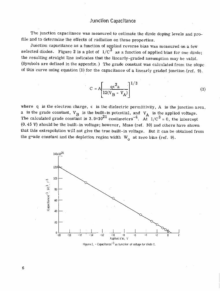
Junction capacitance as a function of applied reverse bias was measured on a few
selected diodes. Figure 2 is a plot of 1/e3 as a function of applied bias for one diode;
the resulting straight line indicates that the linearly-graded assumption may be valid.
(Symbols are defined in the appendix.) The grade constant was calculated from the slope
of this curve using equation (1) for the capaCitance of a linearly graded junction (ref. 9).
[
2 ] 1/3 e - A qE a 12(VB - VA)
(1)
where q is the electron charge, E is the dielectric permittivity, A is the junction area,
a is the grade constant, VB is the built-in potential, and VA is the applied voltage.
The calculated grade constant is 3. 9x10²¹ centimeters-4 . At 1/e3 = 0, the intercept
(0.45 V) should be the built-in voltage; however, Muss (ref. 10) and others have shown
that this extrapolation will not give the true built-in voltage. But it can be obtained from
the g1"ade constant and the depletion region width W 0 at zero bias (ref. 9).
6
M U ;::;
':' Ci) u c
.;o! 'w '" 0..
'" ~
140x1026
Figure 2. - Capacitance-3 as function of voltage for diode 7.
(2)
where ni is the intrinsic carrier density and W 0 is given by
fA -5. W =- = 2.1x10 cm o C
(3)
o
where Co is the zero bias capacitance. The calculated built-in voltage is 0.77 volt.
The base region doping level can also be calculated from the above data, with the assumption that the junction is linearly graded (see ref. 9):
aWo 16-3 NB =-- = 3.8X10 cm (4)
2
The junction capacitance of these diodes was not significantly affected by radiation
damage at the fast neutron flUfmce of 8. 2X10¹³ neutrons per square centimeter. When a
conservative carrier removal rate of 10 carriers per neutron per centimeter is assumed,
the removal carrier density for this irradiation is 8X10¹⁴ carriers per cubic centimeter
which is approximately 2 percent of the calculated base doping density. The correspond
ing 2- percent decrease in the grade constant would cause a decrease in the junction
capacitance of about 0.7 percent. Changes of this size in the zero-bias capacitance were
observed. However, variations of this size may also be the result of experimental error.
Voltage Regulation Region
The reference, or Zener, voltage of silicon voltage regulator diodes is insensitive
to radiation damage at moderate dose levels. The reference voltage of this type of diode
is maintained by avalanche multiplication; that is, carriers acquire sufficient energy in
the junction field to produce additional electron-hole pairs by impact ionization. The
breakdown voltage at which carrier multiplication becomes infinite is a function of the
grade constant a for a diffused, linearly graded junction. This breakdown voltage in
silicon (ref. 11) is given by
( 5)
7

c: 10-2 t ::J
U
-- Extremes --Median
10-4 '----''---------::'-__ L--'----------:L-__ L-__ L-_------'
20 21 Zener voltage, V
Figu re 3. - Zener voltage as function of current for median and extremes (pre- and postirradiation indistinguishable!.
The 2-percent decrease in the grade constant, due to carrier removal at the neutron fluence of 8. 2X10¹³ neutrons per square centimeter, should produce an increase in the reference voltage of about O. 7 percent. The measured change in the reference voltage
at 200 milliamperes (approximately 50 percent maximum current) was less than 0.6 percent in all cases. Figure 3 shows a plot of the reference voltage as a function of current
for the median and the extremes. The preirradiation and postirradiation cases are indistinguishable. The breakdown knee was somewhat softened in all but three diodes, which showed a slight hardening. It was not possible to identify the radiation damage
mechanism that caused knee softening.
8

The neutron failure dose for these diodes can be estimated, if diode failure is defined
as a 20-percent increase in the nominal Zener voltage. For a conservative carrier
removal rate of 10 carriers per neutron per centimeter, the failure dose for these diodes is approximately 1x10¹⁵ neutrons per square centimeter. Work performed by others
(ref. 2) has shown that radiation-induced changes in the Zener voltage appear at neutron doses of 1015 to 1016 neutrons per square centimeter. It appears that increased junction
area does not affect the radiation tolerance of the Zener voltage.
High Forward Current Region
The forward current at high applied voltages (greater than the built-in voltage)
becomes limited by space charge and other effects. Jonscher (ref. 12) has derived a
relation for space-charge limited current flow:
(6)
where fl is the base minority carrier mobility and d is the width of the base region.
The current-voltage characteristics of all diodes exhibited this behavior before and after
irradiation. Figure 4 is a plot of the square root of the current as a function of the
applied voltage minus the built-in voltage before and after irradiation for the median and
extremes. The decrease in slope due to radiation is too large to be accounted for by
S «
S .....
'" ;::,
'E ~ ... :::l
~
2.6
2.2
1.8
1.4
Preirradiation 1.0
Postirradiation
.6L---~--~----~ __ ~--~----~--~--~~~ o .12
Difference between applied and built-in voltage, VA - VB' V
Figure 4. - Square root of forward current as function of difference between applied and built-in voltage before and after irradiation for mediarl and extremes.
9

TABLE m. - CHANGE IN FORWARD VOLTAGE DROP AND ,
. PREIRRADIATION FORWARD DROP AT 1.0 AND 5.0
Diode Current, I, A
1.0 5.0
Pre irradiation Change, P reirradiation Change, voltage drop, V voltage drop, V
V V
Group A; Zener current, 200 mA
1 0.813 -0.010 0.929 0.117 I 2 .800 .001 .879 .141 3 .808 .012 .905 .202 4 .809 .043 .914 .269 5 .809 .020 .926 .221 6 .798 .107 .878 .157 7 .810 -.013 .917 .133 8 .807 -.040 .917 .009 9 .820 -.022 .939 .091
10 .818 -.032 .926 .037 11 .797 -.030 .871 .155 12 .830 -.030 .958 .086 13 .822 .014 .945 .135 14 .802 .006 .897 .115 15 .809 -.023 .925 .105
rms ------ 0.036 ----- 0.146
Group B; reverse voltage, 11 V
16 0.794 -0.030 0.876 0.024
17 .815 .011 .942 .123 18 .811 .028 .906 .045
19 .795 .031 .876 .022
20 .807 .040 .907 .011
rms ----- 0.030 ----- 0.060
Group C; Zener current, 200±100 mA
21 0.816 -0.018 0.945 0.110
22 .807 .043 .913 -.002
23 .816 .041 .926 .016
24 .812 .044 .924 -.004
25 .816 .049 .919 -.006
rms ----- 0.040 ----- 0.045
10

carrier removal. The mobility change required to account for these slope decreases is
much larger than the mobility changes reported by Stein (ref. 8). It appears that the
slope as given in equation (6) is not appropriate to these diodes.
Table TIl lists the change in forward voltage drop and the pre irradiation forward
voltage drop at 1. 0 and 5.0 amperes for all diodes. The operating mode during irradi
ation appears to affect the forward voltage drop, particularly at higher currents as can
be noted in table TIl at 5.0 amperes. This dependence on operating mode was also noticed
in the average decreases in slope of 53, 38, and 28 percent for groups A, B, and C,
respectively.
Effects of Decreased Ca rrier Lifeti me
Neutron irradiation introduces recombination levels in the band gap which results
in decreased carrier lifetimes. These decreased lifetimes produce increases in the
reverse bias leakage current and in the low forward currents at forward biases below
the built- in voltage.
The reverse-leakage current and the low forward current (at biases up to 400 mV
for these diodes) in silicon are recombination-generation currents. The current is given by (ref. 13)
qn i WA I =---- __ ~_L_ f(b)
VTnoTpo kT
where T and T are the minority carrier lifetimes in p- and n-type material, no Po
respectively, and
-qV A/2kT ~(ET - E.) (p)~ b = e cosh 1 + 2 In ~
kT T no
where ET - Ei is the difference between the trap level and the center of the band gap;
then for b < 1. 0
(7)
(8)
11

f(b) = 1
(1 2)1/2 ~-b
b (9)
( 2)1/2 1 - b
and for b > 1. 0
f(b) = 1 In
h 2 )1/2
(J )1/2 b +b2 - 1
(I 2 )1/2
(10)
2\b - 1 b - \b - 1
At forward biases above about .400 millivolts, there is a significant contribution to the
forward current due to diffusion current, which becomes dominant as the applied bias
approaches the built- in potential. The diffusion current is given by (ref. 9)
(11)
where np is the electron concentration in the base, Dn is the electron diffusion constant,
and Ln is the electron diffusion length.
Calculation of the slopes of In I versus V in various regions indicated that equa
tions (8) and (12) describe these diodes. Values of the carrier lifetimes and effective
trap level were calculated from the forward characteristics of the diodes by applying
these equations at three voltage points as follows:
The base minority carrier lifetime Tn was calculated at 700 milivolts using equa-o
tion (12). Equation (8) was applied at 100 and 250 millivolts where recombination-
generation current dominates. At 250 millivolts, b was assumed to be small so that
f(b) is approximately 1[/2, and the hole lifetime Tp was calculated. These lifetimes o
wez:e then used at 100 millivolts to obtain a value of f(b), and then b was taken from a
curve. The trap level was then calculated from
ET - Ei -1 ~ qV A/2kT) 1 (po~ --- = ± cosh be - - In --kT 2 T
no
(12)
12

-- Calculated o Experimental
w- ll L-_----l __ --L __ -L __ -L __ --.L __ 1-_---.!
o .1 .2 .3 .4 .5 .6 .7 Forward bias, V
Figure 5. - Compdrison of experimental and calculated forward characteristics for diode 1 (typical I.
13
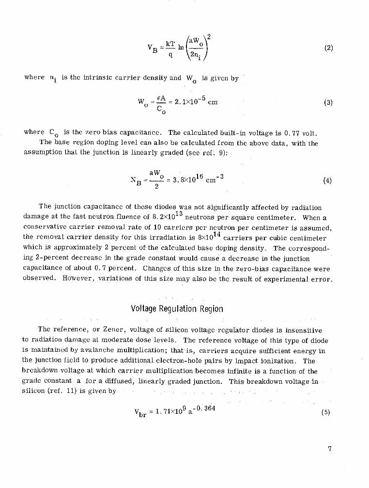
These calculations were made for each diode before and after irradiation, and the
values were used to generate the forward and reverse characteristics. Figures 5 and 6
are plots of the calculated curves with the experimental points indicated for a typical
diode (1) before irradiation. The agreement of calculated with experimental values below
1. 0 volt in the reverse direction indicates that the calculated lifetimes are realistic.
The deviation above 1. O-volt reverse bias in figure 6 is due to the onset of carrier multiplication, which is not a function of minority carrier lifetime. In all other regions, the
agreement of calculated and experimental values was good for all diodes before and after
irradiation.
Table IV presents the calculated carrier lifetimes and the square root of their pro
duct before and after irradiation. As can be seen in the table, the mean electron life
time (25 diodes) decreased by a factor of 37. The mean hole lifetime decreased by a
factor of 3. The mean effective lifetime, defined as rTno Tpo decreased by a factor
of 10.
At reverse biases greater than several kT / q, equation (7) can be approximated as
(ref. 13)
(13)
Calculated o Experi mental
o
o
o o
o
Reverse bias, V
Figure 6. - Comparison of experimental and calculated reverse characteristics for diode 1 (typical).
14

TABLE IV. - MINORITY CARRIER LIFETIMES AND EFFECTIVE LIFETIME
BEFORE AND AFTER IRRADIA TION AND DAMAGE CONSTANT
Diode Preirradiation Postirradiation Damage constant,
Minority carrier Mean Minority carrier Mean KT , lifetime, effective lifetime, effective linvt)(secTI -1
sec lifetime, sec lifetime,
In p-type In n-type f~' In p-type In n-type fu' material, material, o no material, material,
Po no
Tn ' sec sec
Tp , T n ' Tp ,
0 0 0 0 sec sec sec sec
Group A; Zener current, 200 mA
1 2.5XlO- 6 2.3X10- B 2.4X10- 7 6.7X10- 8 1. 7X10- 8 3.3XlO- 8 3.1x10- 7
2 2.5 1.7 2.1 5.1 .83 2.1 3.4
3 2.0 6.7 3.6 5.4 3.3 4.2 2.6 4 2.2 5.1 3.3 6.5 .61 2.0 5.9 5 2.2 7.3 4.0 8.0 2.3 4.2 2.6 6 .99 2.7 1.6 2.5 .81 1.4 7.B
7 1.8 .33 .77 5.7 .65 1.9 4.8 8 1.9 2.0 1.9 5.7 1.4 2.8 3.8
9 2.7 5.8 4.0 5.4 3.1 4.1 2.7 10 1.7 4.2 2.3 7.2 1.0 2.7 4.0
11 1.4 2.2 1.B 5.1 1.4 2.7 3.9 12 7.1 2.6 4.2 11. 0 2.6 5.4 2.0 13 3.0 2.4 2.7 B.2 .55 2.3 4.4
14 1.2 20.0 4.9 3.7 1.9 2.6 4.4 15 1.9 B.O 3.9 6.5 2.0 3.6 3.1
Mean 2.3xlO- 6 4.9X10- 8 2.9X10- 7 6.2x10- B 1. 6x10- B 3.0x10- 8 3.9x10- 7
Group B; reverse voltage, 11 V
16 1. 2XIO- 6 6.0X10- B 2.7X10- 7 5.6XlO- B 0.59x10- B 1. 9X10- B 6.3XlO- 7
17 2.5 3.6 3.0 9.1 .59 2.B 4.9
18 2.9 5.5 4.0 7.3 .54 2.0 3.4
19 1.3 2.4 1.B 5.1 .59 1.7 6.4
20 2.3 4.B 3.3 5.1 .74 1.9 6.0
Mean 2.0X10- 6 4.5XlO- B 2.9xlO- 7 6.4X10- B 0.60X10- B 2.1X10- B 5.4X10- 7
Group C; Zener current, 200 rnA ± 100 mA
21 3.0X10- 6 0.79x10- B 1.5X10- 7 B.BX10- B 1. 7x10- B 3.9xlO- B 2.4x10- 7
22 2.2 2.3 2.2 6.B .70 2.2 5.1
23 4.7 5.3 5.0 B.6 1.6 3.7 3.0
24 2.7 4.3 3.5 7.2 2.0 3.7 2.9
25 3.5 4.4 3.9 6.5 1.3 2.7 3.9
Mean 3.2X10⁻⁶ 3.4X10-B 3.2X10- 7 7.6X10- B 1. 5X10- B 3.2X10- B 3.5X10- 7
15
Preirradiation
== Post irradiation
/
~ /
I / / /
/ / / / I /
// II
_------.-/.-// //1/1
------- / / -- /' / ------- --,..,....../ / -- --./ -- --./ /'
/ ~---- ----.- ....- ------- -----~ ---- ------------ --------'-- -------- ---------- ----- --/--
.-/
10 Reverse bias, V
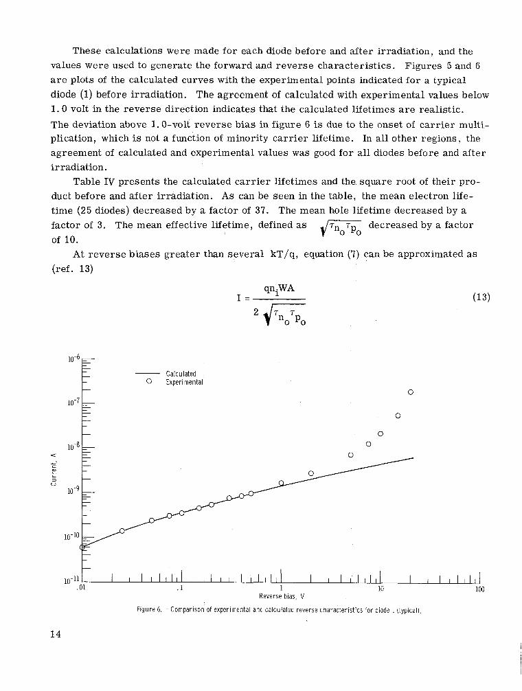
Figure 7. - Reverse leakage current as function of voltage before and after irradiation for median and extremes.
where W, the depletion region width, is the only voltage dependent factor. The effect
100
of radiation damage can be determined from the effective lifetime which has been defined
previously. The agreement of the observed changes in reverse-leakage current with
changes in the effective lifetimes calculated for each diode was excellent for biases up
to about 1 volt where carrier multiplication beginS. The variation in leakage current
among the diodes is considerable, but, in general, the lower the initial leakage, the
larger the increase. Figure 7 is a plot of reverse leakage current as a function of
applied bias for the median and the extremes before and after irradiation.
At low forward biases (below 400 m V), the equation for recombination-generation
current (7) cannot be greatly Simplified. The mean increase in forward current at these
biases was approximately elevenfold. In this region, the increase in current is due to a
decrease in the effective lifetime and also to an increase in f(b). The lifetime decrease
is the dominant effect, producing a factor of 10 increase in current. The remaining
16

Preirradiation
== _ Postirradiation
10-11 L-_-L __ .L..-_-L __ .L..-_--L_--l
o .2 .4 .6 .8 1.0 1.2 Forward bias, V
Figure 8. - Forward current as function of voltage before and after irradiation for median and extremes.
17

current increase can be accounted by the increase in f(b), which is due primarily to the
decrease in the ratio of the minority carrier lifetimes (eq. (8». The trap level was
calculated to lie about 4 kT below the center of the gap and was not significantly changed
by radiation. Figure 8 is a plot of.the forward current as a function of voltage for the
median and the extremes before and after irradiation.
A t moderate forward biases (from about 400 m V up to the built- in voltage of O. 77 V),
the forward current is dominated by diffusion current (eq. (11». The mean increase in
diffusion current was approximately elevenfold. This is in fair agreement with the change
in the square root of the base minority carrier lifetime T (see table IV). no
The radiation induced change in the lifetime is defined in terms of a damage constant
KT
, which is the change in the inverse lifetime per unit neutron fluence:
(14)
where T R is the effective lifetime after irradiation, TO is the initial effective lifetime,
and cp is the total neutron fluence. The damage constants were calculated for these
diodes in terms of the effective lifetimes as defined in equation (13). The values are
shown in table IV. There appears to be a difference in the damage constant due to oper
ating mode, but data scatter makes interpretation uncertain. Bilinski, et al., (ref. 14)
present a compilation of experimental damage constants for silicon which range from
4X10- 8 to 4X10- 6 «sec)(neutron)/cm2)-1.
SUMMARY OF RESULTS
Twenty-five voltage-regulator (Zener) diodes (SlN2985) were exposed to reactor
radiation to a fast-neutron fluence of 8X10¹³ neutrons per square centimeter and a gamma
ray dose of 6x10 7 carbon. The following results were obtained:
1. The effects of neutron-induced carrier removal were negligible at this dose level;
that is, those electrical characteristics that are dependent on carrier concentration were
not significantly affected.
a. Junction capacitance was unchanged. The maximum increase in the Zener
voltage at 100 milliamperes was less than 1 percent.
b. The breakdown knees were slightly softened.
2. The forward voltage drop at high current levels increased, in general, and the
amount of increase was affected by the electrical operating conditions during irradiation.
These effects were not explainable by current theory.
18
3. The minority-carrier lifetimes were decreased: the mean electron lifetime by a
factor of 37 and the mean hole lifetime by a factor of 3. a. These lifetime decreases caused about a factor of 10 increase in the reverse
leakage current and the forward current at biases below 400 millivolts.
b. The decrease in the electron lifetime also produces the factor of 11 increase
in the forward current at biases between 400 and 700 millivolts.
Lewis Research Center,
National Aeronautics and Space Administration,
Cleveland, OhiO, August 22, 1968, 120-27-04-35-22.
19

A
a
b
c
d
f(b)
I
IR 1
20
APPENDIX - SYMBOLS
junction area, cm2
grade constant, cm-4
parameter determined by trap
level, lifetime, and applied
bias
junction capacitance, F
junction capacitance at zero
bias, F
electron diffusion constant,
cm2/sec
base region width, em
separation of trap level from
center of gap, eV
function of b
current, A
reverse current at 18.8 V and
250 C, pA
reverse current at 18.8 V and
2500 C, pA
maximum Zener current, A
maximum surge current, A
Zener test current, mA
damage constant, (nvt)(sec)-l
Boltzmann's constant times
temperature, eV
electron diffusion length, cm
doping dens ity in bas e, cm - 3
intrinsic carrier concentration, -3 cm
E
f1
electron concentration in base, -3 cm
electron charge, C
applie:i voltage, V
built-in voltage, V
breakdown voltage, V
Zener voltage, V
voltage regulation, V
depletion region width, cm
depletion region width at zero
bias, cm
Zener impedance at 1. 0 mA,
ohm
Zener impedance at I zT ' ohms
dielectric permittivity of silicon,
F/cm
minority carrier mobility,
cm2/(V)(sec)
minority carrier lifetime in
p-type material, sec
preirradiation effective life
time, sec
minority carrier lifetime in
n-type material, sec
postirradiation effective life
time, sec
fast neutron fluence,
neutrons/ cm2

REFERENCES
1. Been, Julian F.: Effects of Nuclear Radiation on a High-Reliability Silicon Power
Diode. I - Change in 1- V Design Characteristics. NASA TN D-4620, 1968.
2. Thatcher, R. K.;Hamman, D. J.;Chapin, W. E.; Hanks, C. L.;andWyler, E. N.:
The Effect of Nuclear Radiation on Electronic Components, Including Semicon
ductors. Rep. REIC 36, Battelle Memorial Inst., Oct. 1, 1964. (Available from
DDC as AD-454707. )
3. Lockridge, R. W.: Screening SpeCification for Semiconductor Devices S1N2970B
thru S1N2985B. Specification 85 M01307, NASA George C. Marshall Space Flight
Center, Apr. 1963.
4. Smith, John R.; Kroeger, Erich W.; Asadourian, Arman S.; and Spagnuolo,
Adolph C.: Fast-Neutron Beam Irradiation Facility in the NASA Plum Brook Test
Reactor. NASA TM X-1374, 1967.
5. Bozek, John M. ; and Godlewski, Michael P.: Experimental Determination of Neutron
Fluxes in Plum Brook Reactor HB-6 FaCility with Use of Sulfur Pellets and Gold
Foils. NASA TM X-1497, 1968.
6. Bloomfield, Harvey S.: Calculation of Fast-Neutron Flux Emerging From a Reactor
Beamhole and Comparison with Experiment. NASA TM X-1418, 1967.
7. Bozek, John M.: Experimental Determination of Gamma Exposure Rate in Plum
Brook HB-6 Facility. NASA TM X-1490, 1968.
8. Stein, H. J.: Introduction Rate of Electrically Active Defects in n-Type Silicon by
Nuclear Radiation. Rep. SC-DC-65-1274, Sandia Corp., June 25, 1965.
9. Moll, John L.: Physics of Semiconductors. McGraw-Hill Book Co., Inc., 1964.
10. Muss, D. R.: Capacitance Measurements on Alloyed Indium-Germanium Junction
Diodes. J. Appl. Phys., vol. 26, no. 12, Dec. 1955, pp. 1514-1517.
11. Phillips, A. B.: Transistor Engineering: An Introduction to Integrated Semicon
dlictor Circuits. McGraw-Hill Book Co., Inc., 1962.
12. Jonscher, A. K.: Principles of Semiconductor Device Operation. John Wiley &
Sons, Inc., 1960.
13. Sah, Chik-Tarry; Noyce, Robert N.; and Shockley, William: Carrier Generation
and Recombination of P-N Junctions and P-N Junction Characteristics. Proc.
mE, vol. 45, no. 9, Sept. 1957, pp. 1228-1243.
15. Bilinski, J. R.; Brooks, E. H.; Cocca, U.; and Maier, R. J.: Proton-Neutron
Damage Equivalence in Si and Ge Semiconductors. IEEE Trans. on Nucl. Sci.,
vol. NS-10, no. 5, Nov. 1963, pp. 71-86.
NASA-Langley, 1968 - 28 E- 4396 21

NATIONAL AERONAUTICS AND SPACE ADMINISTRATION WASHINGTON, D. C. 20546
OFFICIAL BUSINESS FIRST CLASS MAIL
POSTAGE AND FEES PAID NATIONAL AERONAUTICS AND
SPACE ADMINISTRATION
POSTMASTER: If Undeliverable (Section 158 Postal Manual) Do Not Return
liThe aeronautical and space activities of the United States shall be conducted so as to contribute ... to the expansion of human knowledge of phenomena in the atmosphere and space. The Administration shall provide for the widest practicable and appropriate dissemination of information concerning its activities and the results thereof."
- NATIONAL AERONAUTICS AND SPACE ACT OF 1958
NASA SCIENTIFIC AND TECHNICAL PUBLICATIONS
TECHNICAL REPORTS: Scientific and technical information considered important, complete, and a lasting contribution to existing knowledge.
TECHNICAL NOTES: Information less broad in scope but nevertheless of importance as a contribution to existing knowledge.
TECHNICAL MEMORANDUMS: Information receiving limited distribution because of preliminary data, security classification, or other reasons.
CONTRACTOR REPORTS: Scientific and technical information generated under a NASA contract or grant and considered an important contribution to existing knowledge.
TECHNICAL TRANSLATIONS: Information published in a foreign language considered to merit NASA distribution in English.
SPECIAL PUBLICATIONS: Information derived from or of value to NASA activities. Publications include conference proceedings, monographs, data compilations, handbooks, source books, and special bibliographies.
TECHNOLOGY UTILIZATION PUBLICATIONS: Information on technology used by ~SA that may be of particular interest in commercial and other non-aerospace applications. Publications include Tech Briefs, Technology Utilization Reports and Notes, and Technology Surveys.
Details on the availability of these publications may be obtained from:
SCIENTIFIC AND TECHNICAL INFORMA nON DIVISION
NATIONAL AERONAUTICS AND SPACE ADMINISTRATION Washington, D.C. 20546