nanya 70nm ddr3 a die specialty datasheet - elixir … · n2cb1gh80bn 1gb ddr3 b-die sdram...
TRANSCRIPT
N2CB1GH80BN 1Gb DDR3 B-Die SDRAM Preliminary
REV 0.1 1 05/2011
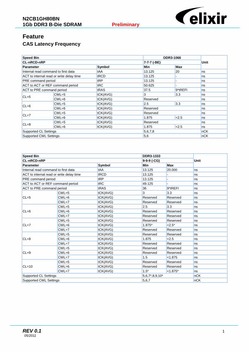
Feature
CAS Latency Frequency
Speed Bin DDR3-1066
Unit CL-nRCD-nRP 7-7-7 (-BE)
Parameter Symbol Min Max
Internal read command to first data tAA 13.125 20 ns
ACT to internal read or write delay time tRCD 13.125 - ns
PRE command period tRP 13.125 - ns
ACT to ACT or REF command period tRC 50.625 - ns
ACT to PRE command period tRAS 37.5 9*tREFI ns
CL=5 CWL=5 tCK(AVG) 3 3.3 ns
CWL=6 tCK(AVG) Reserved ns
CL=6 CWL=5 tCK(AVG) 2.5 3.3 ns
CWL=6 tCK(AVG) Reserved ns
CL=7 CWL=5 tCK(AVG) Reserved ns
CWL=6 tCK(AVG) 1.875 <2.5 ns
CL=8 CWL=5 tCK(AVG) Reserved ns
CWL=6 tCK(AVG) 1.875 <2.5 ns
Supported CL Settings 5,6,7,8 nCK
Supported CWL Settings 5,6 nCK
Speed Bin DDR3-1333
Unit CL-nRCD-nRP 9-9-9 (-CG)
Parameter Symbol Min Max
Internal read command to first data tAA 13.125 20.000 ns
ACT to internal read or write delay time tRCD 13.125 - ns
PRE command period tRP 13.125 - ns
ACT to ACT or REF command period tRC 49.125 - ns
ACT to PRE command period tRAS 36 9*tREFI ns
CL=5
CWL=5 tCK(AVG) 3 3.3 ns
CWL=6 tCK(AVG) Reserved Reserved ns
CWL=7 tCK(AVG) Reserved Reserved ns
CL=6
CWL=5 tCK(AVG) 2.5 3.3 ns
CWL=6 tCK(AVG) Reserved Reserved ns
CWL=7 tCK(AVG) Reserved Reserved ns
CL=7
CWL=5 tCK(AVG) Reserved Reserved ns
CWL=6 tCK(AVG) 1.875* <2.5* ns
CWL=7 tCK(AVG) Reserved Reserved ns
CL=8
CWL=5 tCK(AVG) Reserved Reserved ns
CWL=6 tCK(AVG) 1.875 <2.5 ns
CWL=7 tCK(AVG) Reserved Reserved ns
CL=9
CWL=5 tCK(AVG) Reserved Reserved ns
CWL=6 tCK(AVG) Reserved Reserved ns
CWL=7 tCK(AVG) 1.5 <1.875 ns
CL=10
CWL=5 tCK(AVG) Reserved Reserved ns
CWL=6 tCK(AVG) Reserved Reserved ns
CWL=7 tCK(AVG) 1.5* <1.875* ns
Supported CL Settings 5,6,7*,8,9,10* nCK
Supported CWL Settings 5,6,7 nCK

N2CB1GH80BN 1Gb DDR3 B-Die SDRAM Preliminary
REV 0.1 2 05/2011
1.5V ± 0.075V (JEDEC
Standard Power Supply)
8 Internal memory banks (BA0- BA2)
Differential clock input (CK, )
Programmable Latency: 5, 6, 7, 8, 9, 10
POSTED CAS ADDITIVE Programmable Additive
Latency: 0, CL-1, CL-2
Programmable Sequential / Interleave Burst Type
Programmable Burst Length: 4, 8
8n-bit prefetch architecture
Output Driver Impedance Control
Differential bidirectional data strobe
Write Leveling
OCD Calibration
Dynamic ODT (Rtt_Nom & Rtt_WR)
Auto Self-Refresh
Self-Refresh Temperature
RoHS Compliance
Packages:
78-Ball BGA for x8 components
Description
The 1Gb Double-Data-Rate-3 (DDR3) B-Die DRAMs is double data rate architecture to achieve high-speed operation. It is
internally configured as an eight bank DRAM.
The chip is designed to comply with all key DDR3 DRAM key features and all of the control and address inputs are
synchronized with a pair of externally supplied differential clocks. Inputs are latched at the cross point of differential clocks
(CK rising and falling). All I/Os are synchronized with a single ended DQS or differential DQS pair in a source
synchronous fashion.
These devices operate with a single 1.5V ± 0.075V power supply and are available in BGA packages.

N2CB1GH80BN 1Gb DDR3 B-Die SDRAM Preliminary
REV 0.1 3 05/2011
Pins Configuration – 78 balls BGA Package (X8)
< TOP View>
See the balls through the package
A
B
C
D
E
F
G
x 8
1
VS
S
VSS
Q
VDD
VSS
Q
DQ2
DQ6
VDDQ
VS
S
2
NC
DQ0
DQS
DQ4
3 7 8 9
BA
0
VDD
NC
VS
S
VSS
Q
DQ3
VS
S
DQ5
VS
S
VDD
NU/
DM/TDQS
DQ1
DQ7
CK
VDDQ
H
J
K
L
VS
S
VDDQ
VREFDQ
A3
A 5VS
S
VDD
BA
2
A0
A2 A1
A12
/
NC
A10/A
P
VDD
A4
BA
1
VERFCA
ZQ
VDDQ
VSS
Q
VSS
Q
VDD
ODT
VS
S
NC
M
N
VDD A7
A9
A13
VDDA6
A8
A11
A14VS
S
VS
S
NC
NC
VDD
VS
S
VS
S
CK
E

N2CB1GH80BN 1Gb DDR3 B-Die SDRAM Preliminary
REV 0.1 4 05/2011
Input / Output Functional Description
Symbol Type Function
CK, Input Clock: CK and are differential clock inputs. All address and control input signals are
sampled on the crossing of the positive edge of CK and negative edge of .
CKE, (CKE0),
(CKE1) Input
Clock Enable: CKE high activates, and CKE low deactivates, internal clock signals
and device input buffers and output drivers. Taking CKE low provides Precharge
Power-Down and Self-Refresh operation (all banks idle), or Active Power-Down (row
Active in any bank). CKE is synchronous for power down entry and exit and for
Self-Refresh entry. CKE is asynchronous for Self-Refresh exit. After VREF has
become stable during the power on and initialization sequence, it must be maintained
for proper operation of the CKE receiver. For proper self-refresh entry and exit, VREF
must maintain to this input. CKE must be maintained high throughout read and write
accesses. Input buffers, excluding CK, , ODT and CKE are disabled during Power
Down. Input buffers, excluding CKE, are disabled during Self-Refresh.
, (), (),
(), () Input
Chip Select: All commands are masked when is registered high. provides for
external rank selection on systems with multiple memory ranks. is considered part
of the command code.
, , Input Command Inputs: , and (along with ) define the command being
entered.
DM, (DMU, DML) Input
Input Data Mask: DM is an input mask signal for write data. Input data is masked when
DM is sampled HIGH coincident with that input data during a Write access. DM is
sampled on both edges of DQS. For x8 device, the function of DM or TDQS / is
enabled by Mode Register A11 setting in MR1
BA0 - BA2
Input
Bank Address Inputs: BA0, BA1, and BA2 define to which bank an Active, Read,
Write or Precharge command is being applied. Bank address also determines which
mode register is to be accessed during a MRS cycle.
A10 / AP Input
Auto-Precharge: A10 is sampled during Read/Write commands to determine whether
Autoprecharge should be performed to the accessed bank after the Read/Write
operation. (HIGH: Autoprecharge; LOW: no Autoprecharge). A10 is sampled during a
Precharge command to determine whether the Precharge applies to one bank (A10
LOW) or all banks (A10 HIGH). If only one bank is to be precharged, the bank is
selected by bank addresses.
A0 – A13 Input
Address Inputs: Provide the row address for Activate commands and the column
address for Read/Write commands to select one location out of the memory array in
the respective bank. (A10/AP and A12/ have additional function as below.) The
address inputs also provide the op-code during Mode Register Set commands.
Symbol Type Function

N2CB1GH80BN 1Gb DDR3 B-Die SDRAM Preliminary
REV 0.1 5 05/2011
A12/ Input Burst Chop: A12/is sampled during Read and Write commands to determine if
burst chop (on the fly) will be performed. (HIGH - no burst chop; LOW - burst chopped).
ODT, (ODT0),
(ODT1) Input
On Die Termination: ODT (registered HIGH) enables termination resistance internal
to the DDR3 SDRAM. When enabled, ODT is applied to each DQ, DQS, and
DM/TDQS, NU/ (when TDQS is enabled via Mode Register A11=1 in MR1) signal
for x8 configurations. The ODT pin will be ignored if Mode-registers, MR1and MR2, are
programmed to disable RTT.
Input
Active Low Asynchronous Reset: Reset is active when is LOW, and inactive
when is HIGH. must be HIGH during normal operation. is a
CMOS rail to rail signal with DC high and low at 80% and 20% of VDD, i.e. 1.20V for
DC high and 0.30V
DQ Input/output Data Inputs/Output: Bi-directional data bus.
DQL,
DQU,
DQS,(),
DQSL,(),
DQSU,(),
Input/output
Data Strobe: output with read data, input with write data. Edge aligned with read data,
centered with write data. The data strobes DQS, DQSL, DQSU are paired with
differential signals , , , respectively, to provide differential pair signaling
to the system during both reads and writes. DDR3 SDRAM supports differential data
strobe only and does not support single-ended.
TDQS, () Output
Termination Data Strobe: TDQS/ is applicable for X8 DRAMs only. When
enabled via Mode Register A11=1 in MR1, DRAM will enable the same termination
resistance function on TDQS/ that is applied to DQS/. When disabled via
mode register A11=0 in MR1, DM/ will provide the data mask function and
is not used. x16 DRAMs must disable the TDQS function via mode register A11=0 in
MR1.
NC - No Connect: No internal electrical connection is present.
VDDQ Supply DQ Power Supply: 1.5V ± 0.075V
VDD Supply Power Supply: 1.5V ± 0.075V
VSSQ Supply DQ Ground
Vss Supply Ground
VREFCA Supply Reference voltage for CA
VREFDQ Supply Reference voltage for DQ
ZQ Supply Reference pin for ZQ calibration.
Note: Input only pins (BA0-BA2, A0-A13, , , , , CKE, ODT, and ) do not supply termination.

N2CB1GH80BN 1Gb DDR3 B-Die SDRAM Preliminary
REV 0.1 6 05/2011
DDR3 SDRAM Addressing
Configuration N2CB1GH80BN
# of Bank 8
Bank Address BA0 – BA2
Auto precharge A10 / AP
BL switch on the fly A12 /
Row Address A0 – A13
Column Address A0 – A9
Page size 1KB
Note:
Page size is the number of data delivered from the array to the internal sense amplifiers when an ACTIVE command is
registered. Page size is per bank, calculated as follows:
Page size = 2 COLBITS
* ORG / 8
COLBITS = the number of column address bits
ORG = the number of I/O (DQ) bits

N2CB1GH80BN 1Gb DDR3 B-Die SDRAM Preliminary
REV 0.1 7 05/2011
Ordering Information
Organization Part Number Package Speed
Clock (MHz) Data Rate (Mb/s) CL-TRCD-TRP
128M x 8 N2CB1GH80BN-BE 78-Ball WBGA
0.8mmx0.8mm Pitch
533 DDR3-1066 7-7-7
N2CB1GH80BN-CG 667 DDR3-1333 9-9-9
Simplified State Diagram
Power
ON
Power
Applied Reset
Procedure
From any
State RESET
Initialization
ZQ Calibration Idle
MRS, MPR,
Write
LevelizingSelf Refresh
Refreshing
SRE
SRX
REF
Activating
ACT
Precharge
Power
Down
PDE
PDX
Active
Power
Down
Bank
Active
Writing
Writing
Precharging
Reading
Write
Write A Read A
Write Read
Write A Read A
Write
Read
PRE,
PREA
PRE,
PREA
Write ARead A
PRE,
PREA
PDX
PDE
Reading
Read
Automatic
Sequence
Command
Sequence
MRSZQCL
ZQCL
ZQCS

N2CB1GH80BN 1Gb DDR3 B-Die SDRAM Preliminary
REV 0.1 8 05/2011
State Diagram Command Definitions
Abbreviation Function Abbreviation Function Abbreviation Function
ACT Active Read RD, RDS4, RDS8 PED Enter Power-down
PRE Precharge Read A RDA, RDAS4, RDAS8 PDX Exit Power-down
PREA Precharge All Write WR, WRS4, WRS8 SRE Self-Refresh entry
MRS Mode Register Set Write A WRA, WRAS4, WRAS8 SRX Self-Refresh exit
REF Refresh Start RESET Procedure MPR Multi-Purpose Register
ZQCL ZQ Calibration Long ZQCS ZQ Calibration Short - -

N2CB1GH80BN 1Gb DDR3 B-Die SDRAM Preliminary
REV 0.1 9 05/2011
Basic Functionality
The DDR3 SDRAM B-Die is a high-speed dynamic random access memory internally configured as an eight-bank DRAM.
The DDR3 SDRAM uses an 8n prefetch architecture to achieve high speed operation. The 8n prefetch architecture is
combined with an interface designed to transfer two data words per clock cycle at the I/O pins. A single read or write
operation for the DDR3 SDRAM consists of a single 8n-bit wide, four clock data transfer at the internal DRAM core and
two corresponding n-bit wide, one-half clock cycle data transfers at the I/O pins.
Read and write operation to the DDR3 SDRAM are burst oriented, start at a selected location, and continue for a burst
length of eight or a „chopped‟ burst of four in a programmed sequence. Operation begins with the registration of an Active
command, which is then followed by a Read or Write command. The address bits registered coincident with the Active
command are used to select the bank and row to be activated (BA0-BA2 select the bank; A0-A13 select the row). The
address bit registered coincident with the Read or Write command are used to select the starting column location for the
burst operation, determine if the auto precharge command is to be issued (via A10), and select BC4 or BL8 mode „on the
fly‟ (via A12) if enabled in the mode register.
Prior to normal operation, the DDR3 SDRAM must be powered up and initialized in a predefined manner. The following
sections provide detailed information covering device reset and initialization, register definition, command descriptions
and device operation.
RESET and Initialization Procedure
Power-up Initialization sequence
The Following sequence is required for POWER UP and Initialization
1. Apply power ( is recommended to be maintained below 0.2 x VDD, all other inputs may be undefined).
needs to be maintained for minimum 200μs with stable power. CKE is pulled “Low” anytime before being
de-asserted (min. time 10ns). The power voltage ramp time between 300mV to VDDmin must be no greater than 200ms;
and during the ramp, VDD>VDDQ and (VDD-VDDQ) <0.3 Volts.
- VDD and VDDQ are driven from a single power converter output, AND
- The voltage levels on all pins other than VDD, VDDQ, VSS, VSSQ must be less than or equal to VDDQ and VDD on one
side and must be larger than or equal to VSSQ and VSS on the other side. In addition, VTT is limited to 0.95V max once
power ramp is finished, AND
- Vref tracks VDDQ/2.
OR
- Apply VDD without any slope reversal before or at the same time as VDDQ.
- Apply VDDQ without any slope reversal before or at the same time as VTT & Vref.
- The voltage levels on all pins other than VDD, VDDQ, VSS, VSSQ must be less than or equal to VDDQ and VDD on one
side and must be larger than or equal to VSSQ and VSS on the other side.
2. After is de-asserted, wait for another 500us until CKE become active. During this time, the DRAM will start

N2CB1GH80BN 1Gb DDR3 B-Die SDRAM Preliminary
REV 0.1 10 05/2011
internal state initialization; this will be done independently of external clocks.
3. Clock (CK, ) need to be started and stabilized for at least 10ns or 5tCK (which is larger) before CKE goes active.
Since CKE is a synchronous signal, the corresponding set up time to clock (t IS) must be meeting. Also a NOP or
Deselect command must be registered (with tIS set up time to clock) before CKE goes active. Once the CKE registered
“High” after Reset, CKE needs to be continuously registered “High” until the initialization sequence is finished,
including expiration of tDLLK and tZQinit.
4. The DDR3 DRAM will keep its on-die termination in high impedance state as long as is asserted. Further, the
DRAM keeps its on-die termination in high impedance state after de-assertion until CKE is registered HIGH.
The ODT input signal may be in undefined state until tIS before CKE is registered HIGH. When CKE is registered
HIGH, the ODT input signal may be statically held at either LOW or HIGH. If RTT_NOM is to be enabled in MR1, the
ODT input signal must be statically held LOW. In all cases, the ODT input signal remains static until the power up
initialization sequence is finished, including the expiration of tDLLK and tZQinit.
5. After CKE being registered high, wait minimum of Reset CKE Exit time, tXPR, before issuing the first MRS command
to load mode register. [tXPR=max (tXS, 5tCK)]
6. Issue MRS command to load MR2 with all application settings. (To issue MRS command for MR2, provide “Low” to
BA0 and BA2, “High” to BA1)
7. Issue MRS command to load MR3 with all application settings. (To issue MRS command for MR3, provide “Low” to
BA2, “High” to BA0 and BA1)
8. Issue MRS command to load MR1 with all application settings and DLL enabled. (To issue “DLL Enable” command,
provide “Low” to A0, “High” to BA0 and “Low” to BA1 and BA2)
9. Issue MRS Command to load MR0 with all application settings and “DLL reset”. (To issue DLL reset command,
provide “High” to A8 and “Low” to BA0-BA2)
10. Issue ZQCL command to starting ZQ calibration.
11. Wait for both tDLLK and tZQinit completed.
12. The DDR3 SDRAM is now ready for normal operation.

N2CB1GH80BN 1Gb DDR3 B-Die SDRAM Preliminary
REV 0.1 11 05/2011
Reset and Initialization Sequence at Power- on Ramping (Cont’d)
CK
CK
tCKSRX
RESET
CKE
tIS
ODT
Command
BA0-BA2
T=200us T=500us tXPR tMRD tMRD tMRD tMOD tZQinit.
Do Not
CareTime break
10ns
MRSMRS MRS MRS ZQCL
MR2 MR3 MR1 MR0
VDD,
VDDQ
* From time point Td until Tk. NOP or DES commands must be applied between MRS and ZQcal commnads.
Te Tk
NOP* NOP* Valid
ValidStatic LOW in case RTT_Nom is enabled at time Tg, otherwise static HIGH or LOW
TdTcTa Tb Tf Tg Th Ti Tj
tDLLK
Valid
Valid
Reset Procedure at Stable Power (Cont’d)
The following sequence is required for RESET at no power interruption initialization.
1. Asserted RESET below 0.2*VDD anytime when reset is needed (all other inputs may be undefined). RESET needs to be
maintained for minimum 100ns. CKE is pulled “Low” before RESET being de-asserted (min. time 10ns).
2. Follow Power-up Initialization Sequence step 2 to 11.
3. The Reset sequence is now completed. DDR3 SDRAM is ready for normal operation.
Reset Procedure at Power Stable Condition
CK
CK
tCKSRX
RESET
CKE
tIS
ODT
Command
BA0-BA2
T=100ns T=500us tXPR tMRD tMRD tMRD tMOD tZQinit.
Do Not
CareTime break
10ns
MRSMRS MRS MRS ZQCL
MR2 MR3 MR1 MR0
VDD,
VDDQ
* From time point Td until Tk. NOP or DES commands must be applied between MRS and ZQcal commnads.
Te Tk
NOP* NOP* Valid
ValidStatic LOW in case RTT_Nom is enabled at time Tg, otherwise static HIGH or LOW
TdTcTa Tb Tf Tg Th Ti Tj
tDLLK
Valid
Valid
N2CB1GH80BN 1Gb DDR3 B-Die SDRAM Preliminary
REV 0.1 12 05/2011
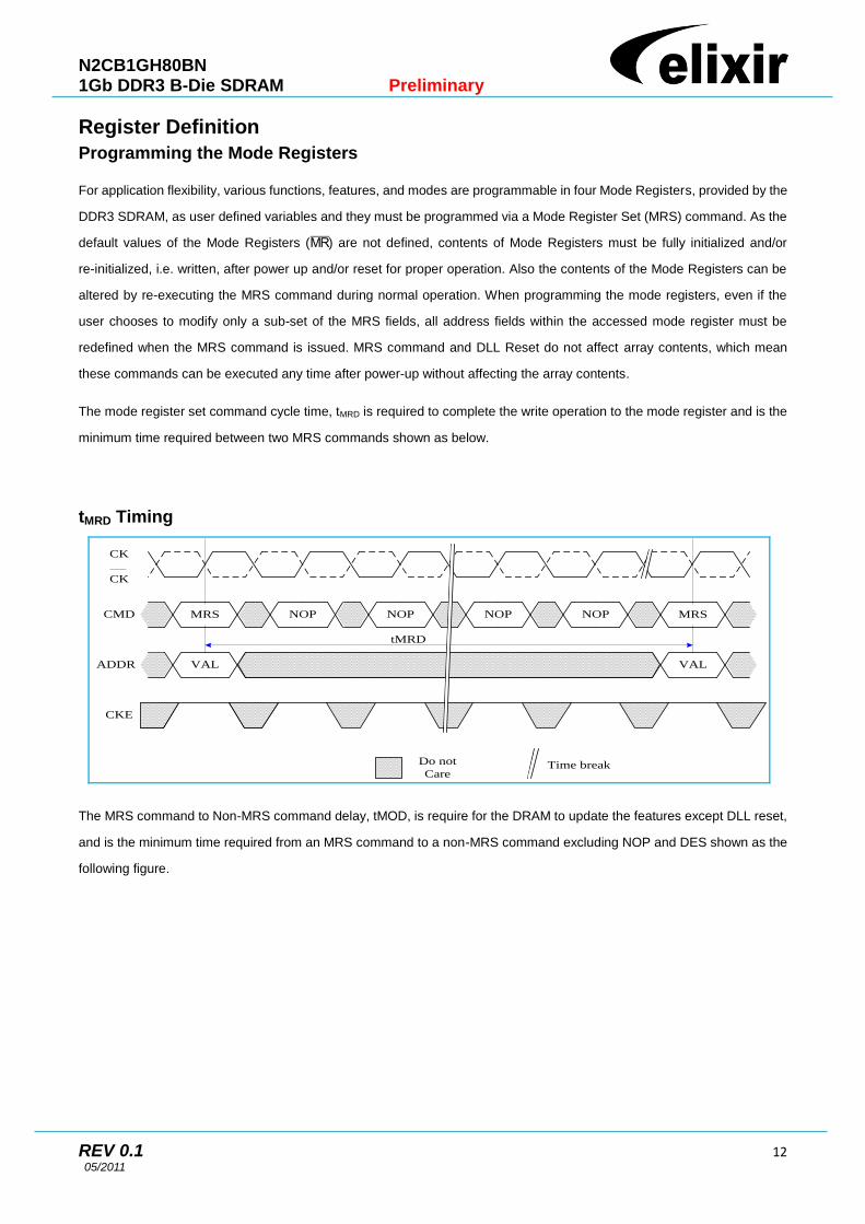
Register Definition
Programming the Mode Registers
For application flexibility, various functions, features, and modes are programmable in four Mode Registers, provided by the
DDR3 SDRAM, as user defined variables and they must be programmed via a Mode Register Set (MRS) command. As the
default values of the Mode Registers () are not defined, contents of Mode Registers must be fully initialized and/or
re-initialized, i.e. written, after power up and/or reset for proper operation. Also the contents of the Mode Registers can be
altered by re-executing the MRS command during normal operation. When programming the mode registers, even if the
user chooses to modify only a sub-set of the MRS fields, all address fields within the accessed mode register must be
redefined when the MRS command is issued. MRS command and DLL Reset do not affect array contents, which mean
these commands can be executed any time after power-up without affecting the array contents.
The mode register set command cycle time, tMRD is required to complete the write operation to the mode register and is the
minimum time required between two MRS commands shown as below.
tMRD Timing
CK
CK
CKE
Do not
CareTime break
MRS NOP NOP NOP NOPCMD
VAL VALADDR
tMRD
MRS
The MRS command to Non-MRS command delay, tMOD, is require for the DRAM to update the features except DLL reset,
and is the minimum time required from an MRS command to a non-MRS command excluding NOP and DES shown as the
following figure.

N2CB1GH80BN 1Gb DDR3 B-Die SDRAM Preliminary
REV 0.1 13 05/2011
tMOD Timing
CK
CK
CKE
MRS NOP NOP NOP NOPCMD
ADDR
tMOD
Non
MRS
VAL
Old Setting Updating Setting New Setting
VAL
VAL
Programming the Mode Registers (Cont’d)
The mode register contents can be changed using the same command and timing requirements during normal operation as
long as the DRAM is in idle state, i.e. all banks are in the precharged state with tRP satisfied, all data bursts are completed
and CKE is high prior to writing into the mode register. The mode registers are divided into various fields depending on the
functionality and/or modes.
Mode Register MR0
The mode-register MR0 stores data for controlling various operating modes of DDR3 SDRAM. It controls burst length, read
burst type, CAS latency, test mode, DLL reset, WR, and DLL control for precharge Power-Down, which include various
vendor specific options to make DDR3 SDRAM useful for various applications. The mode register is written by asserting
low on , , , , BA0, BA1, and BA2, while controlling the states of address pins according to the following
figure.

N2CB1GH80BN 1Gb DDR3 B-Die SDRAM Preliminary
REV 0.1 14 05/2011
MR0 Definition
A0A1A 2A 3A 4A 5A 6A 7A 8A 9A10A11A12A131BA 2
Address Filed
BLA0A1
8 (Fixed)00
BC 4 or 8 (on the fly)
10
Burst Length
Read Burst
TypeA3
Nibble
Sequential0
Interleave1
Burst Type
MRS modeBA 0BA1
MR 000
10
MRS mode
01
11
DLL Control for
Precharge PDA12
Slow Exit ( DLL off )0
Fast Exit (DLL on)1
Precharge Power Down
*
WR(cycles)A 9A10A11
16000
5100
Write recovery for autoprecharge **
010
110
001
101
011
111
DLL ResetA8
NO0
YES1
DLL ResetModeA7
Normal0
TEST1
Mode
* BA 2 and A13 are reserved for future use and must be set to 0 when
programming the MR .
**WR(write recovery for autoprecharge ) min in clock cycles is calculated by
dividing tWR (ns) by tCK (ns ) and rounding up to the next integer:
Wrmin [cycles ] = Roundup(tWR /tCK). The value in the mode register must
be programmed to be equal or larger than WRmin. The programmed WR
value is used with tRP to determine tDAL .
CAS LatencyA 2A 4A5
000
(5)0
CAS Latency
01
11
BC 4 (Fixed)
Reserved
Reserved
A6
0
0 1 0
0 1 0 0
0 1 1 0
1 0 0 0
1 0 1 0
1 1 0 0
1 1 1 0
6
7
8
9
106
7
8
10
12
14
MR 1
MR 2
MR 3
BA 0BA
11
0 0 0
0
1
0 1 1
0 1 1
1 1 1
0
0
1 10 0 16
15
14
13
12
1
1
1
0 1 1
1 10
1 1 1
Reserved
Reserved
Reserved
Reserved

N2CB1GH80BN 1Gb DDR3 B-Die SDRAM Preliminary
REV 0.1 15 05/2011
Burst Length, Type, and Order
Accesses within a given burst may be programmed to sequential or interleaved order. The burst type is selected via bit A3
as shown in the MR0 Definition as above figure. The ordering of access within a burst is determined by the burst length,
burst type, and the starting column address. The burst length is defined by bits A0-A1. Burst lengths options include fix BC4,
fixed BL8, and on the fly which allow BC4 or BL8 to be selected coincident with the registration of a Read or Write
command via A12/.
Burst Type and Burst Order
Burst
Length
Read
Write
Starting
Column
Address
(A2,A1,A0)
Burst type:
Sequential
(decimal)
A3 = 0
Burst type:
Interleaved
(decimal)
A3 = 1
Note
4
Chop
Read
0 , 0 , 0 0 , 1 , 2 , 3 , T , T , T , T 0 , 1 , 2 , 3 , T , T , T , T
1,2,3
0 , 0 , 1 1 , 2 , 3 , 0 , T , T , T , T 1 , 0 , 3 , 2 , T , T , T , T
0 , 1 , 0 2 , 3 , 0 , 1 , T , T , T , T 2 , 3 , 0 , 1 , T , T , T , T
0 , 1 , 1 3 , 0 , 1 , 2 , T , T , T , T 3 , 2 , 1 , 0 , T , T , T , T
1 , 0 , 0 4 , 5 , 6 , 7 , T , T , T , T 4 , 5 , 6 , 7 , T , T , T , T
1 , 0 , 1 5 , 6 , 7 , 4 , T , T , T , T 5 , 4 , 7 , 6 , T , T , T , T
1 , 1 , 0 6 , 7 , 4 , 5 , T , T , T , T 6 , 7 , 4 , 5 , T , T , T , T
1 , 1 , 1 7 , 4 , 5 , 6 , T , T , T , T 7 , 6 , 5 , 4 , T , T , T , T
Write 0 , V , V 0 ,1 ,2 ,3 , X , X , X , X 0 ,1 ,2 ,3 , X , X , X , X
1,2,4,5 1 , V , V 4 ,5 ,6 ,7 , X , X , X , X 4 ,5 ,6 ,7 , X , X , X , X
8 Read
0 , 0 , 0 0 , 1 , 2 , 3 , 4 , 5 , 6 , 7 0 , 1 , 2 , 3 , 4 , 5 , 6 , 7
2
0 , 0 , 1 1 , 2 , 3 , 0 , 5 , 6 , 7 , 4 1 , 0 , 3 , 2 , 5 , 4 , 7 , 6
0 , 1 , 0 2 , 3 , 0 , 1 , 6 , 7 , 4 , 5 2 , 3 , 0 , 1 , 6 , 7 , 4 , 5
0 , 1 , 1 3 , 0 , 1 , 2 , 7 , 4 , 5 , 6 3 , 2 , 1 , 0 , 7 , 6 , 5 , 4
1 , 0 , 0 4 , 5 , 6 , 7 , 0 , 1 , 2 , 3 4 , 5 , 6 , 7 , 0 , 1 , 2 , 3
1 , 0 , 1 5 , 6 , 7 , 4 , 1 , 2 , 3 , 0 5 , 4 , 7 , 6 , 1 , 0 , 3 , 2
1 , 1 , 0 6 , 7 , 4 , 5 , 2 , 3 , 0 , 1 6 , 7 , 4 , 5 , 2 , 3 , 0 , 1
1 , 1 , 1 7 , 4 , 5 , 6 , 3 , 0 , 1 , 2 7 , 6 , 5 , 4 , 3 , 2 , 1 , 0
Write V , V , V 0 , 1 , 2 , 3 , 4 , 5 , 6 , 7 0 , 1 , 2 , 3 , 4 , 5 , 6 , 7 2,4
Note:
1. In case of burst length being fixed to 4 by MR0 setting, the internal write operation starts two clock cycles earlier
than the BL8 mode. This means that the starting point for tWR and tWTR will be pulled in by two clocks. In case of
burst length being selected on-the-fly via A12/, the internal write operation starts at the same point in time like a
burst of 8 write operation. This means that during on-the-fly control, the starting point for tWR and tWTR will not be
pulled in by two clocks.
2. 0~7 bit number is value of CA [2:0] that causes this bit to be the first read during a burst.
3. T: Output driver for data and strobes are in high impedance.
4. V: a valid logic level (0 or 1), but respective buffer input ignores level on input pins.
5. X: Do not Care.
N2CB1GH80BN 1Gb DDR3 B-Die SDRAM Preliminary
REV 0.1 16 05/2011
CAS Latency
The CAS Latency is defined by MR0 (bit A9~A11) as shown in the MR0 Definition figure. CAS Latency is the delay, in clock
cycles, between the internal Read command and the availability of the first bit of output data. DDR3 SDRAM does not
support any half clock latencies. The overall Read Latency (RL) is defined as Additive Latency (AL) + CAS Latency (CL);
RL = AL + CL.
Test Mode
The normal operating mode is selected by MR0 (bit7=0) and all other bits set to the desired values shown in the MR0
definition figure. Programming bit A7 to a „1‟ places the DDR3 SDRAM into a test mode that is only used by the DRAM
manufacturer and should not be used. No operations or functionality is guaranteed if A7=1.
DLL Reset
The DLL Reset bit is self-clearing, meaning it returns back to the value of „0‟ after the DLL reset function has been issued.
Once the DLL is enabled, a subsequent DLL Reset should be applied. Anytime the DLL reset function is used, tDLLK must
be met before any functions that require the DLL can be used (i.e. Read commands or ODT synchronous operations.)
Write Recovery
The programmed WR value MR0(bits A9, A10, and A11) is used for the auto precharge feature along with tRP to determine
tDAL WR (write recovery for auto-precharge)min in clock cycles is calculated by dividing tWR(ns) by tCK(ns) and rounding
up to the next integer: WRmin[cycles] = Roundup(tWR[ns]/tCK[ns]). The WR must be programmed to be equal or larger
than tWR (min).
Precharge PD DLL
MR0 (bit A12) is used to select the DLL usage during precharge power-down mode. When MR0 (A12=0), or „slow-exit‟, the
DLL is frozen after entering precharge power-down (for potential power savings) and upon exit requires tXPDLL to be met
prior to the next valid command. When MR0 (A12=1), or „fast-exit‟, the DLL is maintained after entering precharge
power-down and upon exiting power-down requires tXP to be met prior to the next valid command.
N2CB1GH80BN 1Gb DDR3 B-Die SDRAM Preliminary
REV 0.1 17 05/2011
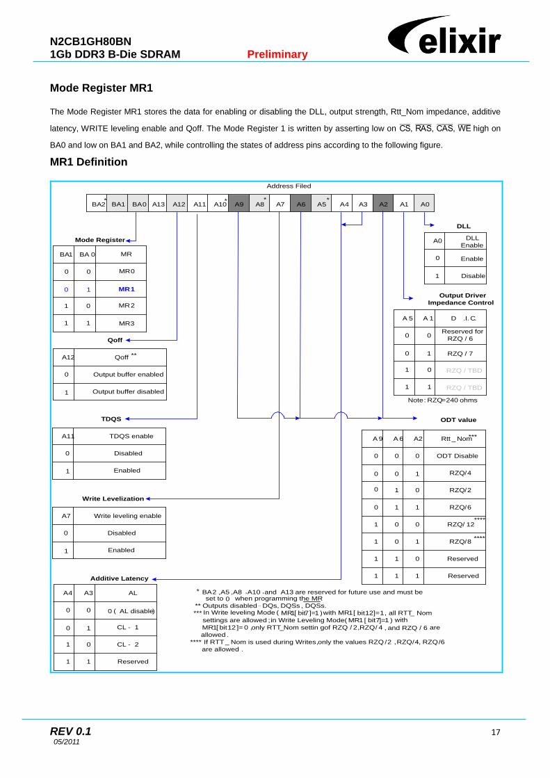
Mode Register MR1
The Mode Register MR1 stores the data for enabling or disabling the DLL, output strength, Rtt_Nom impedance, additive
latency, WRITE leveling enable and Qoff. The Mode Register 1 is written by asserting low on , , , high on
BA0 and low on BA1 and BA2, while controlling the states of address pins according to the following figure.
MR1 Definition
A0A1A2A3A4A5A6A7A8A9A10A11A12A13BA0BA1BA2
Address Filed
DLL
EnableA0
Enable0
Disable1
DLL
Output Driver
Impedance Control
MRBA 0BA1
MR000
MR110
Mode Register
01
11 MR3
MR2
Qoff
*
* BA2 , A5 , A8 , A10 , and A13 are reserved for future use and must be set to 0 when programming the MR.
** Outputs disabled – DQs, DQSs , DQSs.
*** In Write leveling Mode ( MR1[ bit7]=1 ) with MR1[ bit12]=1, all RTT_ Nom
settings are allowed ; in Write Leveling Mode ( MR1 [ bit7]=1 ) with
MR1[ bit12 ]= 0 , only RTT_Nom settin gof RZQ / 2, RZQ/ 4 , and RZQ / 6 are
allowed .
**** If RTT _ Nom is used during Writes, only the values RZQ/2 , RZQ/4, RZQ/6
are allowed .
QoffA12
Output buffer enabled0
Output buffer disabled1
ALA3A4
0 ( AL disable)00
CL - 110
Additive Latency
01
11
Rtt _ Nom A2A 6A 9
ODT Disable000
100
010
110
001
101
011
111
ODT value
RZQ/4
RZQ/2
RZQ/6
RZQ/ 12
RZQ/8
Reserved
Reserved
*
CL - 2
Reserved
* *
Write Levelization
Write leveling enableA7
Disabled0
Enabled1
TDQS
TDQS enableA11
Disabled0
Enabled1
D .I. C.A 1A 5
Reserved for
RZQ / 600
RZQ / 710
01
11
**
***
Note: RZQ=240 ohms
****
****
RZQ / TBD
RZQ / TBD

N2CB1GH80BN 1Gb DDR3 B-Die SDRAM Preliminary
REV 0.1 18 05/2011
DLL Enable/Disable
The DLL must be enabled for normal operation. DLL enable is required during power up initialization, and upon returning to
normal operation after having the DLL disabled. During normal operation (DLL-on) with MR1 (A0=0), the DLL is
automatically disabled when entering Self-Refresh operation and is automatically re-enable upon exit of Self-Refresh
operation. Any time the DLL is enabled and subsequently reset, tDLLK clock cycles must occur before a Read or
synchronous ODT command can be issued to allow time for the internal clock to be synchronized with the external clock.
Failing to wait for synchronization to occur may result in a violation of the tDQSCK, tAON, or tAOF parameters. During
tDLLK, CKE must continuously be registered high. DDR3 SDRAM does not require DLL for any Write operation, expect
when RTT_WR is enabled and the DLL is required for proper ODT operation. For more detailed information on DLL Disable
operation in DLL-off Mode.
The direct ODT feature is not supported during DLL-off mode. The on-die termination resistors must be disabled by continu-
ously registering the ODT pin low and/or by programming the RTT_Nom bits MR1A9,A6,A2 to 0,0,0 via a mode register
set command during DLL-off mode.
The dynamic ODT feature is not supported at DLL-off mode. User must use MRS command to set Rtt_WR, MR2 A10, A9
= 0, 0, to disable Dynamic ODT externally.
Output Driver Impedance Control
The output driver impedance of the DDR3 SDRAM device is selected by MR1 (bit A1 and A5) as shown in MR1 definition
figure.
ODT Rtt Values
DDR3 SDRAM is capable of providing two different termination values (Rtt_Nom and Rtt_WR). The nominal termination
value Rtt_Nom is programmable in MR1. A separate value (Rtt_WR) may be programmable in MR2 to enable a unique Rtt
value when ODT is enabled during writes. The Rtt_WR value can be applied during writes even when Rtt_Nom is disabled.
Additive Latency (AL)
Additive Latency (AL) operation is supported to make command and data bus efficient for sustainable bandwidth in DDR3
SDRAM. In this operation, the DDR3 SDRAM allows a read or write command (either with or without auto-precharge) to be
issued immediately after the active command. The command is held for the time of the Additive Latency (AL) before it is
issued inside the device. The Read Latency (RL) is controlled by the sum of the AL and CAS Latency (CL) register settings.
Write Latency (WL) is controlled by the sum of the AL and CAS Write Latency (CWL) register settings. A summary of the AL
register options are shown as the following table.

N2CB1GH80BN 1Gb DDR3 B-Die SDRAM Preliminary
REV 0.1 19 05/2011
Additive Latency (AL) Settings
A4 A3 AL
0 0 0, (AL Disable)
0 1 CL-1
1 0 CL-2
1 1 Reserved

N2CB1GH80BN 1Gb DDR3 B-Die SDRAM Preliminary
REV 0.1 20 05/2011
Write leveling
For better signal integrity, DDR3 memory module adopted fly by topology for the commands, addresses, control signals,
and clocks. The fly by topology has benefits from reducing number of stubs and their length but in other aspect, causes
flight time skew between clock and strobe at every DRAM on DIMM. It makes difficult for the Controller to maintain tDQSS,
tDSS, and tDSH specification. Therefore, the controller should support „write leveling‟ in DDR3 SDRAM to compensate for
skew.
Output Disable
The DDR3 SDRAM outputs maybe enable/disabled by MR1 (bit12) as shown in MR1 definition. When this feature is
enabled (A12=1) all output pins (DQs, DQS, , etc.) are disconnected from the device removing any loading of the
output drivers. This feature may be useful when measuring modules power for example. For normal operation A12 should
be set to „0‟.
TDQS,
TDQS (Termination Data Strobe) is a feature of x8 DDR3 SDRAM that provides additional termination resistance outputs
that may be useful in some system configurations.
When enabled via the mode register, the same termination resistance function is applied to be TDQS/ pins that are
applied to the DQS/ pins.
In contrast to the RDQS function of DDR2 SDRAM, TDQS provides the termination resistance function only. The data
strobe function of RDQS is not provided by TDQS.
The TDQS and DM functions share the same pin. When the TDQS function is enabled via the mode register, the DM
function is not supported. When the TDQS function is disabled, the DM function is provided and the pin is not used.
The TDQS function is available in x8 DDR3 SDRAM only and must be disabled via the mode register A11=0 in MR1 for x16
configurations.
TDQS, Function Matrix
MR1 (A11) DM / TDQS NU / TDQS
0 (TDQS Disabled) DM Hi-Z
1 (TDQS Enabled) TDQS
Note:
1. If TDQS is enabled, the DM function is disabled.
2. When not used, TDQS function can be disabled to save termination power.
3. TDQS function is only available for x8 DRAM and must be disabled for x16.

N2CB1GH80BN 1Gb DDR3 B-Die SDRAM Preliminary
REV 0.1 21 05/2011
Mode Register MR2
The Mode Register MR2 stores the data for controlling refresh related features, Rtt_WR impedance, and CAS write latency.
The Mode Register 2 is written by asserting low on , , , high on BA1 and low on BA0 and BA2, while
controlling the states of address pins according to the table below.
MR2 Definition
A0A1A2A3A4A5A6A7A8A9A10A11A12A13BA0BA1BA2
Address Filed
MRS
modeBA0BA1
MR 000
10
MRS mode
01
11
*
* BA2 ,
A5 ,
A8 ,
A 11-A13 are reserved for future use and must be set to 0 when programming the MR.
*
*
The Rtt _WR value can be applied during writes even when Rtt_Nom is disabled
.
During write leveling ,
Dynamic ODT is not available
.
MR 1
MR 2
MR 3
CAS Write LatencyA 3A4
00
0
CAS Write Latency
A5
0
0 1
0 1 0
0 1 1
1 0 0
1 0 1
1 1 0
1 1 1
PASRA0A1
00
Half Array
( 000, 001, 010 ,011)0
PASR
Full Array
A2
0
0 1
0 1 0
0 1 1
1 0 0
1 0 1
1 1 0
1 1 1
Quarter Array
(000 ,001)
1/8th Array (000)
3 / 4 array ( 010 ,
011 ,
100 ,
101,
110 ,
111)
Half array
( 100, 101 ,
110, 111)
Quarter array
( 110 , 111)
1/ 8th
array (111)
AS RA6
Manual Self Refresh Reference0
ASR Enable1
Auto Self Refresh
SRTA7
Normal Operating temperature
range0
Extended operating temperature
range 1
Self - Refresh Temperature Range
A9A10
Dynamic ODT off (Write does
not affect RTT value)00
10
01
11
RZQ / 4
Reserved
Rtt_WR* *
Rtt_WR
RZQ/ 2
12 (0.833 ns >tCK(avg)>=0.75 ns)
11 (0.935 ns >tCK(avg)>=0.833 ns)
10 (1.07 ns >tCK(avg)>=0.935 ns)
9 (1.25 ns >tCK(avg)>=1.07 ns)
8 (1.5 ns >tCK(avg) >=1.25 ns)
7 (1.875 ns >tCK(avg) >=1.5 ns)
6 (2.5 ns >tCK(avg) >=1.875 ns)
5 (tCK(avg) >= 2.5 ns)

N2CB1GH80BN 1Gb DDR3 B-Die SDRAM Preliminary
REV 0.1 22 05/2011
CAS Write Latency (CWL)
The CAS Write Latency is defined by MR2 (bits A3-A5) shown in MR2. CAS Write Latency is the delay, in clock cycles,
between the internal Write command and the availability of the first bit of input data. DDR3 DRAM does not support any half
clock latencies. The overall Write Latency (WL) is defined as Additive Latency (AL) + CAS Write Latency (CWL);
WL=AL+CWL.
For more information on the supported CWL and AL settings based on the operating clock frequency, refer to “Standard
Speed Bins” on page106. For detailed Write operation refer to “WRITE Operation” on page39.
Auto Self-Refresh (ASR) and Self-Refresh Temperature (SRT)
DDR3 SDRAM must support Self-Refresh operation at all supported temperatures. Applications requiring Self-Refresh
operation in the Extended Temperature Range must use the ASR function or program the SRT bit appropriately.
Optional in DDR3 SDRAM: Users should refer to the DRAM supplier data sheet and/or the DIMM SPD to determine if
DDR3 SDRAM devices support the following options or requirements referred to in this material. For more details refer to
“Extended Temperature Usage” on page39. DDR3 SDRAMs must support Self-Refresh operation at all supported
temperatures. Applications requiring Self-Refresh operation in the Extended Temperature Range must use the optional
ASR function or program the SRT bit appropriately.
Dynamic ODT (Rtt_WR)
DDR3 SDRAM introduces a new feature “Dynamic ODT”. In certain application cases and to further enhance signal
integrity on the data bus, it is desirable that the termination strength of the DDR3 SDRAM can be changed without issuing
an MRS command. MR2 Register locations A9 and A10 configure the Dynamic ODT settings.
DDR3 SDRAM introduces a new feature “Dynamic ODT”. In certain application cases and to further enhance signal
integrity on the data bus, it is desirable that the termination strength of the DDR3 SDRAM can be changed without issuing
an MRS command. MR2 Register locations A9 and A10 configure the Dynamic ODT settings. In Write leveling mode, only
RTT_Nom is available. For details on Dynamic ODT operation, refer to “Dynamic ODT” on page66.
N2CB1GH80BN 1Gb DDR3 B-Die SDRAM Preliminary
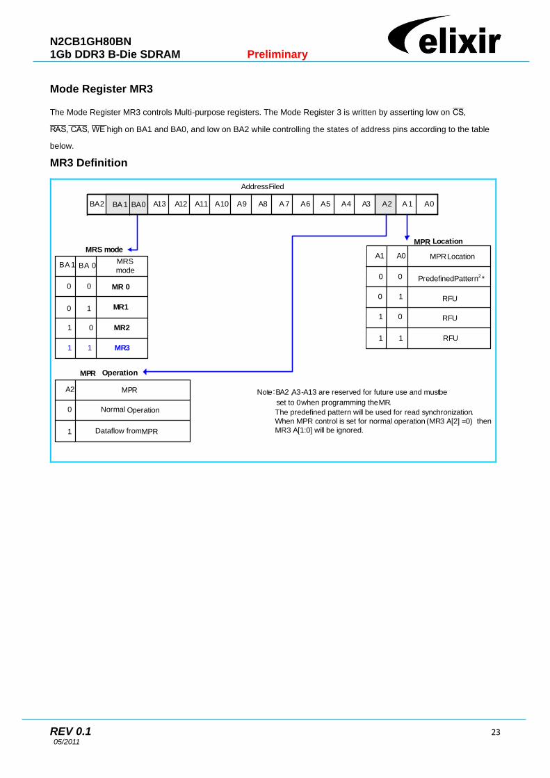
REV 0.1 23 05/2011
Mode Register MR3
The Mode Register MR3 controls Multi-purpose registers. The Mode Register 3 is written by asserting low on ,
,, high on BA1 and BA0, and low on BA2 while controlling the states of address pins according to the table
below.
MR3 Definition
A0A 1A2A3A4A5A6A 7A8A9A10A11A12A13BA0BABA2
Address Filed
MRS
modeBA 0BA 1
MR 000
10
MRS mode
01
11
Note:BA2 ,A3-A13 are reserved for future use and must be
set to 0 when programming the MR.
MR1
MR2
MR3
MPRA2
Normal Operation0
Dataflow from MPR1
MPR
MPR LocationA0A1
00
RFU0
MPR Location
Predefined Pattern *2
1
1 0
1 1
RFU
1
RFU
Operation
The predefined pattern will be used for read synchronization.
When MPR control is set for normal operation (MR3 A[2] =0) then
MR3 A[1:0] will be ignored.

N2CB1GH80BN 1Gb DDR3 B-Die SDRAM Preliminary
REV 0.1 24 05/2011
Multi-Purpose Register (MPR)
The Multi Purpose Register (MPR) function is used to Read out a predefined system timing calibration bit sequence. To
enable the MPR, a Mode Register Set (MRS) command must be issued to MR3 register with bit A2=1. Prior to issuing the
MRS command, all banks must be in the idle state (all banks precharged and tRP met). Once the MPR is enabled, any
subsequent RD or RDA commands will be redirected to the Multi Purpose Register. When the MPR is enabled, only RD or
RDA commands are allowed until a subsequent MRS command is issued with the MPR disabled (MR3 bit A2=0). Power
down mode, Self-Refresh and any other non-RD/RDA command is not allowed during MPR enable mode. The RESET
function is supported during MPR enable mode.
The Multi Purpose Register (MPR) function is used to Read out a predefined system timing calibration bit sequence.
MPR Block Diagram
To enable the MPR, a MODE Register Set (MRS) command must be issued to MR3 Register with bit A2 = 1, as following
Table 1. Prior to issuing the MRS command, all banks must be in the idle state (all banks precharged and tRP met). Once
the MPR is enabled, any subsequent RD or RDA commands will be redirected to the Multi Purpose Register. The resulting
operation, when a RD or RDA command is issued, is defined by MR3 bits A[1:0] when the MPR is enabled as shown on
page26. When the MPR is enabled, only RD or RDA commands are allowed until a subsequent MRS command is issued
with the MPR disabled (MR3 bit A2 = 0). Note that in MPR mode RDA has the same functionality as a READ command
which means the auto precharge part of RDA is ignored. Power-Down mode, Self-Refresh and any other non-RD/RDA
command is not allowed during MPR enable mode. The RESET function is supported during MPR enable mode.
N2CB1GH80BN 1Gb DDR3 B-Die SDRAM Preliminary
REV 0.1 25 05/2011
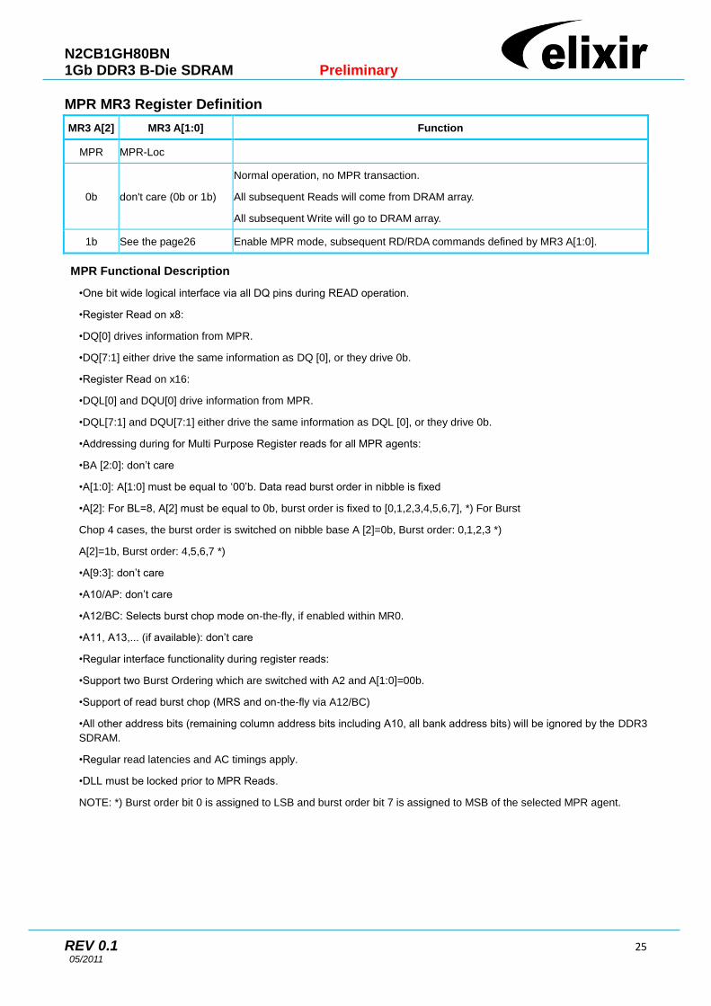
MPR MR3 Register Definition
MR3 A[2] MR3 A[1:0] Function
MPR MPR-Loc
0b don't care (0b or 1b)
Normal operation, no MPR transaction.
All subsequent Reads will come from DRAM array.
All subsequent Write will go to DRAM array.
1b See the page26 Enable MPR mode, subsequent RD/RDA commands defined by MR3 A[1:0].
MPR Functional Description
•One bit wide logical interface via all DQ pins during READ operation.
•Register Read on x8:
•DQ[0] drives information from MPR.
•DQ[7:1] either drive the same information as DQ [0], or they drive 0b.
•Register Read on x16:
•DQL[0] and DQU[0] drive information from MPR.
•DQL[7:1] and DQU[7:1] either drive the same information as DQL [0], or they drive 0b.
•Addressing during for Multi Purpose Register reads for all MPR agents:
•BA [2:0]: don‟t care
•A[1:0]: A[1:0] must be equal to „00‟b. Data read burst order in nibble is fixed
•A[2]: For BL=8, A[2] must be equal to 0b, burst order is fixed to [0,1,2,3,4,5,6,7], *) For Burst
Chop 4 cases, the burst order is switched on nibble base A [2]=0b, Burst order: 0,1,2,3 *)
A[2]=1b, Burst order: 4,5,6,7 *)
•A[9:3]: don‟t care
•A10/AP: don‟t care
•A12/BC: Selects burst chop mode on-the-fly, if enabled within MR0.
•A11, A13,... (if available): don‟t care
•Regular interface functionality during register reads:
•Support two Burst Ordering which are switched with A2 and A[1:0]=00b.
•Support of read burst chop (MRS and on-the-fly via A12/BC)
•All other address bits (remaining column address bits including A10, all bank address bits) will be ignored by the DDR3
SDRAM.
•Regular read latencies and AC timings apply.
•DLL must be locked prior to MPR Reads.
NOTE: *) Burst order bit 0 is assigned to LSB and burst order bit 7 is assigned to MSB of the selected MPR agent.

N2CB1GH80BN 1Gb DDR3 B-Die SDRAM Preliminary
REV 0.1 26 05/2011
MPR MR3 Register Definition
MR3 A[2] MR3 A[1:0] Function Burst Length Read
Address
A[2:0]
Burst Order and Data
Pattern
1b 00b Read Predefined
Pattern for System
Calibration
BL8 000b Burst order 0,1,2,3,4,5,6,7
Pre-defined Data Pattern
[0,1,0,1,0,1,0,1]
BC4 000b Burst order 0,1,2,3
Pre-defined Data Pattern
[0,1,0,1]
BC4 100b Burst order 4,5,6,7
Pre-defined Data Pattern
[0,1,0,1]
1b 01b RFU BL8 000b Burst order 0,1,2,3,4,5,6,7
BC4 000b Burst order 0,1,2,3
BC4 100b Burst order 4,5,6,7
1b 10b RFU BL8 000b Burst order 0,1,2,3,4,5,6,7
BC4 000b Burst order 0,1,2,3
BC4 100b Burst order 4,5,6,7
1b 11b RFU BL8 000b Burst order 0,1,2,3,4,5,6,7
BC4 000b Burst order 0,1,2,3
BC4 100b Burst order 4,5,6,7
NOTE: Burst order bit 0 is assigned to LSB and the burst order bit 7 is assigned to MSB of the selected MPR agent.
N2CB1GH80BN 1Gb DDR3 B-Die SDRAM Preliminary
REV 0.1 27 05/2011
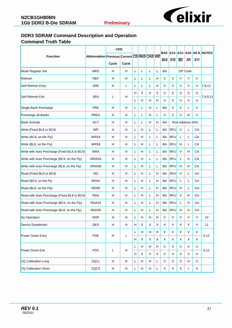
DDR3 SDRAM Command Description and Operation
Command Truth Table
Function Abbreviation
CKE
BA0-
A13-
A12-
A10-
A0-9,
NOTES
Previous
Cycle
Current
Cycle
Mode Register Set MRS H H L L L L BA OP Code
Refresh REF H H L L L H V V V V V
Self Refresh Entry SRE H L L L L H V V V V V 7,9,12
Self Refresh Exit SRX L H H X X X X X X X X
7,8,9,12 L H H H V V V V V
Single Bank Precharge PRE H H L L H L BA V V L V
Precharge all Banks PREA H H L L H L V V V H V
Bank Activate ACT H H L L H H BA Row Address (RA)
Write (Fixed BL8 or BC4) WR H H L H L L BA RFU V L CA
Write (BC4, on the Fly) WRS4 H H L H L L BA RFU L L CA
Write (BL8, on the Fly) WRS8 H H L H L L BA RFU H L CA
Write with Auto Precharge (Fixed BL8 or BC4) WRA H H L H L L BA RFU V H CA
Write with Auto Precharge (BC4, on the Fly) WRAS4 H H L H L L BA RFU L H CA
Write with Auto Precharge (BL8, on the Fly) WRAS8 H H L H L L BA RFU H H CA
Read (Fixed BL8 or BC4) RD H H L H L H BA RFU V L CA
Read (BC4, on the Fly RDS4 H H L H L H BA RFU L L CA
Read (BL8, on the Fly) RDS8 H H L H L H BA RFU H L CA
Read with Auto Precharge (Fixed BL8 or BC4) RDA H H L H L H BA RFU V H CA
Read with Auto Precharge (BC4, on the Fly) RDAS4 H H L H L H BA RFU L H CA
Read with Auto Precharge (BL8, on the Fly) RDAS8 H H L H L H BA RFU H H CA
No Operation NOP H H L H H H V V V V V 10
Device Deselected DES H H H X X X X X X X X 11
Power Down Entry PDE H L L H H H V V V V V
6,12 H X X X X X X X X
Power Down Exit PDX L H
L H H H V V V V V
6,12 H X X X X X X X X
ZQ Calibration Long ZQCL H H L H H L X X X H X
ZQ Calibration Short ZQCS H H L H H L X X X L X

N2CB1GH80BN 1Gb DDR3 B-Die SDRAM Preliminary
REV 0.1 28 05/2011
DDR3 SDRAM Command Description and Operation
Command Truth Table (Conti.)
NOTE1. All DDR3 SDRAM commands are defined by states of , , , and CKE at the rising edge of the clock.
The MSB of BA, RA and CA are device density and configuration dependant.
NOTE2. is Low enable command which will be used only for asynchronous reset so must be maintained HIGH
during any function.
NOTE3. Bank addresses (BA) determine which bank is to be operated upon. For (E)MRS BA selects an (Extended) Mode
Register.
NOTE4. “V” means “H or L (but a defined logic level)” and “X” means either “defined or undefined (like floating) logic level”.
NOTE5. Burst reads or writes cannot be terminated or interrupted and Fixed/on-the-Fly BL will be defined by MRS.
NOTE6. The Power-Down Mode does not perform any refresh operation.
NOTE7. The state of ODT does not affect the states described in this table. The ODT function is not available during Self
Refresh.
NOTE8. Self Refresh Exit is asynchronous.
NOTE9. VREF (Both VrefDQ and VrefCA) must be maintained during Self Refresh operation.
NOTE10. The No Operation command should be used in cases when the DDR3 SDRAM is in an idle or wait state. The
purpose of the No Operation command (NOP) is to prevent the DDR3 SDRAM from registering any unwanted
commands between operations. A No Operation command will not terminate a pervious operation that is still
executing, such as a burst read or write cycle.
NOTE11. The Deselect command performs the same function as No Operation command.
NOTE12. Refer to the CKE Truth Table for more detail with CKE transition.

N2CB1GH80BN 1Gb DDR3 B-Die SDRAM Preliminary
REV 0.1 29 05/2011
CKE Truth Table
Current State
CKE
Command (N)
, ,, Action (N) Notes
Previous
Cycle
(N-1)
Current
Cycle
(N)
Power-Down L L X Maintain Power-Down 14,15
L H DESELECT or NOP Power-Down Exit 11,14
Self-Refresh L L X Maintain Self-Refresh 15,16
L H DESELECT or NOP Self-Refresh Exit 8,12,16
Bank(s) Active H L DESELECT or NOP Active Power-Down Entry 11,13,14
Reading H L DESELECT or NOP Power-Down Entry 11,13,14,17
Writing H L DESELECT or NOP Power-Down Entry 11,13,14,17
Precharging H L DESELECT or NOP Power-Down Entry 11,13,14,17
Refreshing H L DESELECT or NOP Precharge Power-Down Entry 11
All Banks Idle H L DESELECT or NOP Precharge Power-Down Entry 11,13,14,18
H L REFRESH Self-Refresh 9,13,18
NOTE 1 CKE (N) is the logic state of CKE at clock edge N; CKE (N-1) was the state of CKE at the previous clock edge.
NOTE 2 Current state is defined as the state of the DDR3 SDRAM immediately prior to clock edge N.
NOTE 3 COMMAND (N) is the command registered at clock edge N, and ACTION (N) is a result of COMMAND (N), ODT is not included
here.
NOTE 4 All states and sequences not shown are illegal or reserved unless explicitly described elsewhere in this document.
NOTE 5 The state of ODT does not affect the states described in this table. The ODT function is not available during Self-Refresh.
NOTE 6 CKE must be registered with the same value on tCKEmin consecutive positive clock edges. CKE must remain at the valid input
level the entire time it takes to achieve the tCKEmin clocks of registrations. Thus, after any CKE transition, CKE may not
transition from its valid level during the time period of tIS + tCKEmin + tIH.
NOTE 7 DESELECT and NOP are defined in the Command Truth Table.
NOTE 8 On Self-Refresh Exit DESELECT or NOP commands must be issued on every clock edge occurring during the tXS period. Read
or ODT commands may be issued only after tXSDLL is satisfied.
NOTE 9 Self-Refresh modes can only be entered from the All Banks Idle state.
NOTE 10 Must be a legal command as defined in the Command Truth Table.
NOTE 11 Valid commands for Power-Down Entry and Exit are NOP and DESELECT only.
NOTE 12 Valid commands for Self-Refresh Exit are NOP and DESELECT only.
NOTE 13 Self-Refresh cannot be entered during Read or Write operations.
NOTE 14 The Power-Down does not perform any refresh operations.
NOTE 15 “X” means “don‟t care“(including floating around VREF) in Self-Refresh and Power-Down. It also applies to Address pins.
NOTE 16 VREF (Both Vref_DQ and Vref_CA) must be maintained during Self-Refresh operation.
NOTE 17 If all banks are closed at the conclusion of the read, write or precharge command, then Precharge Power-Down is entered,
otherwise Active Power-Down is entered.
NOTE 18 „Idle state‟ is defined as all banks are closed (tRP, tDAL, etc. satisfied), no data bursts are in progress, CKE is high, and all
timings from previous operations are satisfied (tMRD, tMOD, tRFC, tZQinit, tZQoper, tZQCS, etc.) as well as all Self-Refresh
exit and Power-Down Exit parameters are satisfied (tXS, tXP, tXPDLL, etc).

N2CB1GH80BN 1Gb DDR3 B-Die SDRAM Preliminary
REV 0.1 30 05/2011
No Operation (NOP) Command
The No operation (NOP) command is used to instruct the selected DDR3 SDRAM to perform a NOP (low and , ,
and high). This prevents unwanted commands from being registered during idle or wait states. Operations already in
progress are not affected.
Deselect Command
The Deselect function (HIGH) prevents new commands from being executed by the DDR3 SDRAM. The DDR3 SDRAM
is effectively deselected. Operations already in progress are not affected.
DLL- Off Mode
DDR3 DLL-off mode is entered by setting MR1 bit A0 to “1”; this will disable the DLL for subsequent operations until A0 bit
set back to “0”. The MR1 A0 bit for DLL control can be switched either during initialization or later.
The DLL-off Mode operations listed below are an optional feature for DDR3. The maximum clock frequency for DLL-off
Mode is specified by the parameter tCKDLL_OFF. There is no minimum frequency limit besides the need to satisfy the
refresh interval, tREFI.
Due to latency counter and timing restrictions, only one value of CAS Latency (CL) in MR0 and CAS Write Latency (CWL)
in MR2 are supported. The DLL-off mode is only required to support setting of both CL=6 and CWL=6.
DLL-off mode will affect the Read data Clock to Data Strobe relationship (tDQSCK) but not the data Strobe to Data
relationship (tDQSQ, tQH). Special attention is needed to line up Read data to controller time domain.
Comparing with DLL-on mode, where tDQSCK starts from the rising clock edge (AL+CL) cycles after the Read command,
the DLL-off mode tDQSCK starts (AL+CL-1) cycles after the read command. Another difference is that tDQSCK may not be
small compared to tCK (it might even be larger than tCK) and the difference between tDQSCKmin and tDQSCKmax is
significantly larger than in DLL-on mode.
The timing relations on DLL-off mode READ operation have shown at the following Timing Diagram (CL=6, BL=8)

N2CB1GH80BN 1Gb DDR3 B-Die SDRAM Preliminary
REV 0.1 31 05/2011
DLL-off mode READ Timing Operation
Note: The tDQSCK is used here for DQS, DQS, and DQ to have a simplified diagram; the DLL_off shift will affect both timings in the same
way and the skew between all DQ, DQS, and signals will still be tDQSQ.
CK
CK
T0 T1 T2 T3 T4 T5 T6 T7 T8 T9
READCMD
Bank, Col bAddress
Din
b
Din
b+1
Din
b+2
Din
b+3
Din
b+4
Din
b+5
Din
b+6
Din
b+7
DQSdiff_DLL_on
DQ_DLL_on
DQSdiff_DLL_off
DQ_DLL_off
DQSdiff_DLL_off
DQ_DLL_off
RL = AL+CL = 6 (CL=6, AL=0)
RL(DLL_off) = AL+(CL-1) = 5 tDQSCKDLL_diff_min
tDQSCKDLL_diff_max
Din
b
Din
b+1
Din
b+2
Din
b+3
Din
b+4
Din
b+5
Din
b+6
Din
b+7
Din
b
Din
b+1
Din
b+2
Din
b+3
Din
b+4
Din
b+5
Din
b+6
Din
b+7
N2CB1GH80BN 1Gb DDR3 B-Die SDRAM Preliminary
REV 0.1 32 05/2011
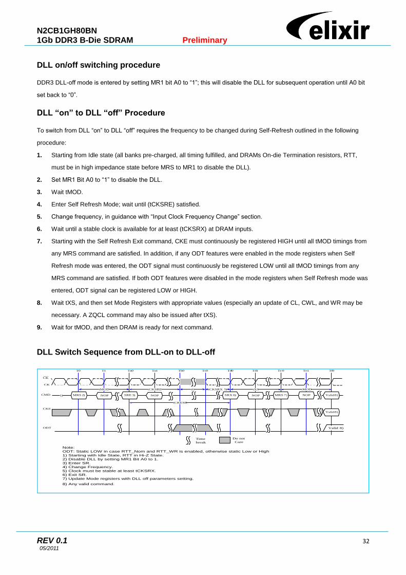
DLL on/off switching procedure
DDR3 DLL-off mode is entered by setting MR1 bit A0 to “1”; this will disable the DLL for subsequent operation until A0 bit
set back to “0”.
DLL “on” to DLL “off” Procedure
To switch from DLL “on” to DLL “off” requires the frequency to be changed during Self-Refresh outlined in the following
procedure:
1. Starting from Idle state (all banks pre-charged, all timing fulfilled, and DRAMs On-die Termination resistors, RTT,
must be in high impedance state before MRS to MR1 to disable the DLL).
2. Set MR1 Bit A0 to “1” to disable the DLL.
3. Wait tMOD.
4. Enter Self Refresh Mode; wait until (tCKSRE) satisfied.
5. Change frequency, in guidance with “Input Clock Frequency Change” section.
6. Wait until a stable clock is available for at least (tCKSRX) at DRAM inputs.
7. Starting with the Self Refresh Exit command, CKE must continuously be registered HIGH until all tMOD timings from
any MRS command are satisfied. In addition, if any ODT features were enabled in the mode registers when Self
Refresh mode was entered, the ODT signal must continuously be registered LOW until all tMOD timings from any
MRS command are satisfied. If both ODT features were disabled in the mode registers when Self Refresh mode was
entered, ODT signal can be registered LOW or HIGH.
8. Wait tXS, and then set Mode Registers with appropriate values (especially an update of CL, CWL, and WR may be
necessary. A ZQCL command may also be issued after tXS).
9. Wait for tMOD, and then DRAM is ready for next command.
DLL Switch Sequence from DLL-on to DLL-off
CK
CK
T0 T1 Ta0 Ta1 Tb0 Tc0 Td0 Td1 Te0 Te1
MRS 2)1)CMD
CKE
ODT
tMOD
Tf0
tCKSRE 4) tCKSRX 5) tXS tMOD
NOP SRE 3) NOP SRX 6) NOP MRS 7) NOP Valid8)
tCKESR
Valid8)
Valid 8)
Time
break
Do not
Care
Note:
ODT: Static LOW in case RTT_Nom and RTT_WR is enabled, otherwise static Low or High
1) Starting with Idle State, RTT in Hi-Z State.
2) Disable DLL by setting MR1 Bit A0 to 1.
3) Enter SR.
4) Change Frequency.
5) Clock must be stable at least tCKSRX.
6) Exit SR.
7) Update Mode registers with DLL off parameters setting.
8) Any valid command.

N2CB1GH80BN 1Gb DDR3 B-Die SDRAM Preliminary
REV 0.1 33 05/2011
DLL “off” to DLL “on” Procedure
To switch from DLL “off” to DLL “on” (with requires frequency change) during Self-Refresh:
1. Starting from Idle state (all banks pre-charged, all timings fulfilled and DRAMs On-die Termination resistors (RTT) must
be in high impedance state before Self-Refresh mode is entered).
2. Enter Self Refresh Mode, wait until tCKSRE satisfied.
3. Change frequency, in guidance with “Input clock frequency change” section.
4. Wait until a stable is available for at least (tCKSRX) at DRAM inputs.
5. Starting with the Self Refresh Exit command, CKE must continuously be registered HIGH until tDLLK timing from
subsequent DLL Reset command is satisfied. In addition, if any ODT features were enabled in the mode registers when
Self Refresh mode was entered. the ODT signal must continuously be registered LOW until tDLLK timings from
subsequent DLL Reset command is satisfied. If both ODT features are disabled in the mode registers when Self
Refresh mode was entered, ODT signal can be registered LOW or HIGH.
6. Wait tXS, then set MR1 Bit A0 to “0” to enable the DLL.
7. Wait tMRD, then set MR0 Bit A8 to “1” to start DLL Reset.
8. Wait tMRD, then set Mode registers with appropriate values (especially an update of CL, CWL, and WR may be
necessary. After tMOD satisfied from any proceeding MRS command, a ZQCL command may also be issued during or
after tDLLK).
9. Wait for tMOD, then DRAM is ready for next command (remember to wait tDLLK after DLL Reset before applying
command requiring a locked DLL!). In addition, wait also for tZQoper in case a ZQCL command was issued.
DLL Switch Sequence from DLL-on to DLL-off
CK
CK
T0 Ta0 Ta1 Tb0 Tc0 Tc1 Td0 Te0 Tf1 Tg0
1)CMD
CKE
ODT
Th0
tCKSRE tCKSRX 4) tXS tMRDtDLLK
NOP SRE 2) SRX 5) MRS 6) MRS 7) MRS 8) Valid
ODTLoff+ 1tck
3) tMRD
Valid
tCKESR
Timebreak
Do notCare
NOP
Note:
ODT: Static LOW in case RTT_Nom and RTT_WR is enabled, otherwise static Low or High
1) Starting from Idle State.
2) Enter SR.
3) Change Frequency.
4) Clock must be stable at least tCKSRX.
5) Exit SR.
6) Set DLL-on by MR1 A0="0"
7) Start DLL Reset
8) Any valid command

N2CB1GH80BN 1Gb DDR3 B-Die SDRAM Preliminary
REV 0.1 34 05/2011
Input Clock frequency change
Once the DDR3 SDRAM is initialized, the DDR3 SDRAM requires the clock to be “stable” during almost all states of normal
operation. This means once the clock frequency has been set and is to be in the “stable state”, the clock period is not
allowed to deviate except for what is allowed for by the clock jitter and SSC (spread spectrum clocking) specification.
The input clock frequency can be changed from one stable clock rate to another stable clock rate under two conditions: (1)
Self-Refresh mode and (2) Precharge Power-Down mode. Outside of these two modes, it is illegal to change the clock
frequency.
For the first condition, once the DDR3 SDRAM has been successfully placed in to Self-Refresh mode and tCKSRE has
been satisfied, the state of the clock becomes a don‟t care. Once a don‟t care, changing the clock frequency is permissible,
provided the new clock frequency is stable prior to tCKSRX. When entering and exiting Self-Refresh mode of the sole
purpose of changing the clock frequency. The DDR3 SDRAM input clock frequency is allowed to change only within the
minimum and maximum operating frequency specified for the particular speed grade.
The second condition is when the DDR3 SDRAM is in Precharge Power-Down mode (either fast exit mode or slow exit
mode). If the RTT_Nom feature was enabled in the mode register prior to entering Precharge power down mode, the ODT
signal must continuously be registered LOW ensuring RTT is in an off state. If the RTT_Nom feature was disabled in the
mode register prior to entering Precharge power down mode, RTT will remain in the off state. The ODT signal can be
registered either LOW or HIGH in this case. A minimum of tCKSRE must occur after CKE goes LOW before the clock
frequency may change. The DDR3 SDRAM input clock frequency is allowed to change only within the minimum and
maximum operating frequency specified for the particular speed grade. During the input clock frequency change, ODT and
CKE must be held at stable LOW levels. Once the input clock frequency is changed, stable new clocks must be provided to
the DRAM tCKSRX before precharge Power Down may be exited; after Precharge Power Down is exited and tXP has
expired, the DLL must be RESET via MRS. Depending on the new clock frequency additional MRS commands may need to
be issued to appropriately set the WR, CL, and CWL with CKE continuously registered high. During DLL re-lock period,
ODT must remain LOW and CKE must remain HIGH. After the DLL lock time, the DRAM is ready to operate with new clock
frequency.

N2CB1GH80BN 1Gb DDR3 B-Die SDRAM Preliminary
REV 0.1 35 05/2011
Change Frequency during Precharge Power-down
NOTES:
1. Applicable for both SLOW EXIT and FAST EXIT Precharge Power-down
2. tAOFPD and tAOF must be statisfied and outputs High-Z prior to T1; refer to ODT timing section for exact requirements
3. If the RTT_NOM feature was enabled in the mode register prior to entering Precharge power down mode, the ODT
signal must continuously be registered LOW ensuring RTT is in an off state. If the RTT_NOM feature was disabled in the mode register
prior to entering Precharge power down mode, RTT will remain in the off state. The ODT signal can be registered either LOW or HIGH in
this case.
CK
CK
T0 T1 T2 Ta0 Tb0 Tc0 Tc1 Td0 Td1 Te0
CKE
Command
DQS,
DQS
tCH tCL
tCK
Te1
tIH tIS tIH tIS
tCKSRE
tCKE
tCKSRX
tCHb tCLbtCKb
NOP NOP NOP NOP NOP MRS NOP Valid
DLL
ResetValid
tIH tIS
Address
ODT
DQ
DM
High-Z
High-Z
tAOFPD/tAOF
tCPDED
tXP
tDLLK
Previous Clock Frequency New Clock Frequency
Frequency
Change
Enter Precharge
Power-Down mode
Exit Precharge
Power-Down mode
N2CB1GH80BN 1Gb DDR3 B-Die SDRAM Preliminary
REV 0.1 36 05/2011
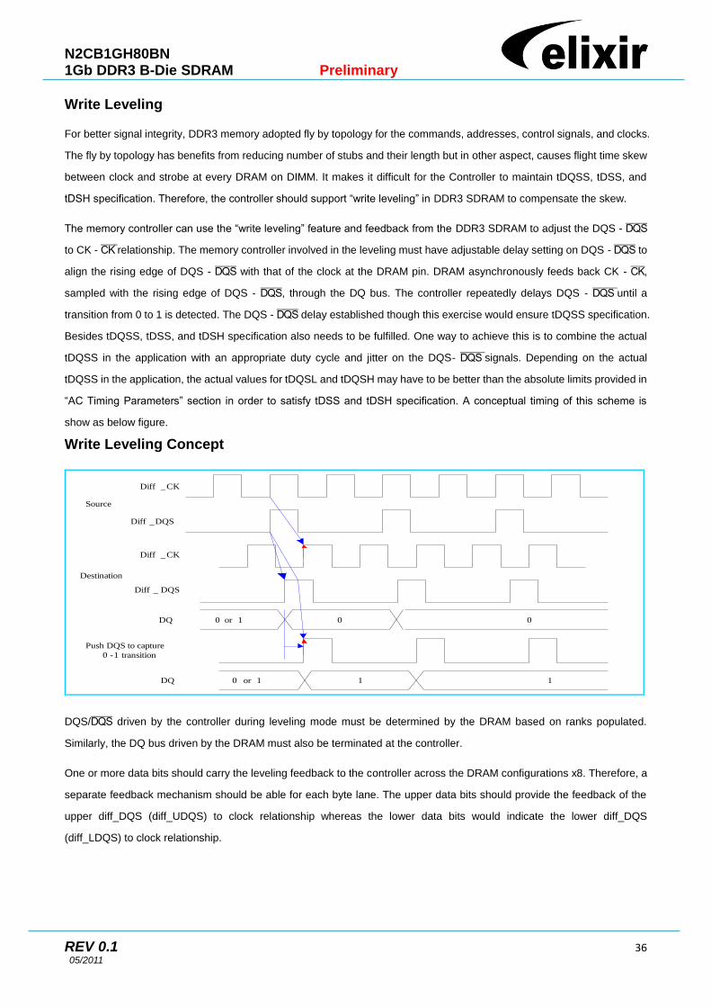
Write Leveling
For better signal integrity, DDR3 memory adopted fly by topology for the commands, addresses, control signals, and clocks.
The fly by topology has benefits from reducing number of stubs and their length but in other aspect, causes flight time skew
between clock and strobe at every DRAM on DIMM. It makes it difficult for the Controller to maintain tDQSS, tDSS, and
tDSH specification. Therefore, the controller should support “write leveling” in DDR3 SDRAM to compensate the skew.
The memory controller can use the “write leveling” feature and feedback from the DDR3 SDRAM to adjust the DQS -
to CK - relationship. The memory controller involved in the leveling must have adjustable delay setting on DQS - to
align the rising edge of DQS - with that of the clock at the DRAM pin. DRAM asynchronously feeds back CK - ,
sampled with the rising edge of DQS - , through the DQ bus. The controller repeatedly delays DQS - until a
transition from 0 to 1 is detected. The DQS - delay established though this exercise would ensure tDQSS specification.
Besides tDQSS, tDSS, and tDSH specification also needs to be fulfilled. One way to achieve this is to combine the actual
tDQSS in the application with an appropriate duty cycle and jitter on the DQS- signals. Depending on the actual
tDQSS in the application, the actual values for tDQSL and tDQSH may have to be better than the absolute limits provided in
“AC Timing Parameters” section in order to satisfy tDSS and tDSH specification. A conceptual timing of this scheme is
show as below figure.
Write Leveling Concept
0 or 1 0 0
Diff _CK
Diff _DQS
Source
Diff _CK
Diff _ DQS
Destination
DQ
DQ
Push DQS to capture
0 -1 transition
0 or 1 1 1
DQS/ driven by the controller during leveling mode must be determined by the DRAM based on ranks populated.
Similarly, the DQ bus driven by the DRAM must also be terminated at the controller.
One or more data bits should carry the leveling feedback to the controller across the DRAM configurations x8. Therefore, a
separate feedback mechanism should be able for each byte lane. The upper data bits should provide the feedback of the
upper diff_DQS (diff_UDQS) to clock relationship whereas the lower data bits would indicate the lower diff_DQS
(diff_LDQS) to clock relationship.
N2CB1GH80BN 1Gb DDR3 B-Die SDRAM Preliminary
REV 0.1 37 05/2011
DRAM setting for write leveling and DRAM termination unction in that mode
DRAM enters into Write leveling mode if A7 in MR1 set “High” and after finishing leveling, DRAM exits from write leveling
mode if A7 in MR1 set “Low”. Note that in write leveling mode, only DQS/terminations are activated and deactivated
via ODT pin not like normal operation.
MR setting involved in the leveling procedure
Function MR1 Enable Disable
Write leveling enable A7 1 0
Output buffer mode (Qoff) A12 0 1
DRAM termination function in the leveling mode
ODT pin at DRAM DQS/ termination DQs termination
De-asserted off off
Asserted on off
Note: In write leveling mode with its output buffer disabled (MR1[bit7]=1 with MR1[bit12]=1) all RTT_Nom settings are allowed; in Write
Leveling Mode with its output buffer enabled (MR1[bit7]=1 with MR1[bit12]=0) only RTT_Nom settings of RZQ/2, RZQ/4, and RZQ/6 are
allowed.
Procedure Description
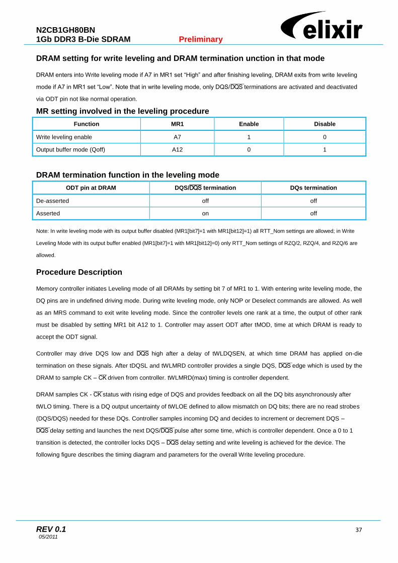
Memory controller initiates Leveling mode of all DRAMs by setting bit 7 of MR1 to 1. With entering write leveling mode, the
DQ pins are in undefined driving mode. During write leveling mode, only NOP or Deselect commands are allowed. As well
as an MRS command to exit write leveling mode. Since the controller levels one rank at a time, the output of other rank
must be disabled by setting MR1 bit A12 to 1. Controller may assert ODT after tMOD, time at which DRAM is ready to
accept the ODT signal.
Controller may drive DQS low and high after a delay of tWLDQSEN, at which time DRAM has applied on-die
termination on these signals. After tDQSL and tWLMRD controller provides a single DQS, edge which is used by the
DRAM to sample CK – driven from controller. tWLMRD(max) timing is controller dependent.
DRAM samples CK - status with rising edge of DQS and provides feedback on all the DQ bits asynchronously after
tWLO timing. There is a DQ output uncertainty of tWLOE defined to allow mismatch on DQ bits; there are no read strobes
(DQS/DQS) needed for these DQs. Controller samples incoming DQ and decides to increment or decrement DQS –
delay setting and launches the next DQS/pulse after some time, which is controller dependent. Once a 0 to 1
transition is detected, the controller locks DQS – delay setting and write leveling is achieved for the device. The
following figure describes the timing diagram and parameters for the overall Write leveling procedure.
N2CB1GH80BN 1Gb DDR3 B-Die SDRAM Preliminary
REV 0.1 38 05/2011
Timing details of Write leveling sequence
DQS - is capturing CK - low at T1 and CK - high at T2
NOP NOP NOP NOP NOP NOP NOP NOP NOP
CK
CK
CMD
ODT
Diff_DQS
Prime DQ
Late Re ma ining
DQs
tMOD
tWLMR D tWLO
tWLS tWLH
tWLOE
tWLS tWLH
tWLO
NOPMRS
tDQSHtDQSLtDQSHtDQSL
T1 T2
Time
break
Do not
Care
One Prime DQ:
Early
Re ma ining
DQs
tWLO
tWLO
Undefined
Driving Mode
tWLOEtWLO
tWLOAll DQs are Prime :
Late Re ma ining
DQs
Early
Re ma ining
DQs
tWLMRD
tWLO
tWLO
tWLOE
tWLDQSEN
NOP
Note:
1. DRAM has the option to drive leveling feedback on a prime DQ or all DQs. If feedback is driven only on
one DQ, the remaining DQs must be driven low as shown in above Figure, and maintained at this state
through out the leveling procedure.
2. MRS: Load MR1 to enter write leveling mode
3. NOP: NOP or deselect
4. diff_DQS is the differential data strobe (DQS, ). Timing reference points are the zero crossings. DQS
is shown with solid line, is shown with dotted line.
6. DQS/ needs to fulfill minimum pulse width requirements tDQSH(min) and tDQSL(min) as defined for
regular Writes; the max pulse width is system dependent.
Write Leveling Mode Exit
The following sequence describes how Write Leveling Mode should be exited:
1. After the last rising strobe edge (see ~T0), stop driving the strobe signals (see ~Tc0). Note: From now on, DQ pins are in
undefined driving mode, and will remain undefined, until tMOD after the respective MR command (Te1).
2. Drive ODT pin low (tIS must be satisfied) and keep it low (see Tb0).
3. After the RTT is switched off, disable Write Level Mode via MRS command (see Tc2).
4. After tMOD is satisfied (Te1), any valid command may be registered. (MR commands may be issued after tMRD (Td1).
N2CB1GH80BN 1Gb DDR3 B-Die SDRAM Preliminary
REV 0.1 39 05/2011
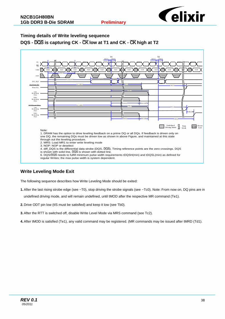
Timing detail of Write Leveling exit
Extended Temperature Usage
Nanya‟s DDR3 SDRAM supports the optional extended temperature range of 0°C to +95°C, TC. Thus, the SRT and ASR
options must be used at a minimum. The extended temperature range DRAM must be refreshed externally at 2X (double
refresh) anytime the case temperature is above +85°C (and does not exceed +95°C). The external refreshing requirement
is accomplished by reducing the refresh period from 64ms to 32ms. However, self refresh mode requires either ASR or
SRT to support the extended temperature. Thus either ASR or SRT must be enabled when TC is above +85°C or self
refresh cannot be used until the case temperature is at or below +85°C.
Table 14 summarizes the two extended temperature options and Table 15 summarizes how the two extended temperature
options relate to one another.
Mode Register Description
Field Bits Description
ASR MR2(A6)
Auto Self-Refresh (ASR)
When enabled, DDR3 SDRAM automatically provides Self-Refresh power management
functions for all supported operating temperature values. If not enabled, the SRT bit must be
programmed to indicate TOPER during subsequent Self-Refresh operation.
0 = Manual SR Reference (SRT)
1 = ASR enable
SRT MR2(A7)
Self-Refresh Temperature (SRT) Range
If ASR = 0, the SRT bit must be programmed to indicate TOPER during subsequent Self-Refresh
operation. If ASR = 1, SRT bit must be set to 0.
0 = Normal operating temperature range
1 = Extended operating temperature range
CK
CK
T0 T1 Ta0 Tc0 Tc1 Tc2 Td1 Te1
CMD
BA
tIS
tMOD
tMRD
ODT
RTT_DQS_DQS
DQS_DQS
Result = 1
tWLO
DQ
RTT_Nom
Td0 Te0T2 Tb0
tAOFmin
tAOFmax
TransitioningTime Break Do not CareUndefined
Driving Mode
NOP NOP NOP NOP NOP NOP NOP MRS NOP Valid NOP Valid
MR1 Valid Valid
tODTLoff

N2CB1GH80BN 1Gb DDR3 B-Die SDRAM Preliminary
REV 0.1 40 05/2011
Auto Self-Refresh mode - ASR mode
DDR3 SDRAM provides an Auto-Refresh mode (ASR) for application ease. ASR mode is enabled by setting MR2 bit A6=1
and MR2 bit A7=0. The DRAM will manage Self-Refresh entry in either the Normal or Extended Temperature Ranges. In
this mode, the DRAM will also manage Self-Refresh power consumption when the DRAM operating temperature changes,
lower at low temperatures and higher at high temperatures. If the ASR option is not supported by DRAM, MR2 bit A6 must
set to 0. If the ASR option is not enabled (MR2 bit A6=0), the SRT bit (MR2 bit A7) must be manually programmed with the
operating temperature range required during Self-Refresh operation. Support of the ASR option does not automatically
imply support of the Extended Temperature Range.
Self-Refresh Temperature Range - SRT
SRT applies to devices supporting Extended Temperature Range only. If ASR=0, the Self-Refresh Temperature (SRT)
Range bit must be programmed to guarantee proper self-refresh operation. If SRT=0, then the DRAM will set an
appropriate refresh rate for Self-Refresh operation in the Normal Temperature Range. If SRT=1, then the DRAM will set an
appropriate, potentially different, refresh rate to allow Self-Refresh operation in either the Normal or Extended Temperature
Ranges. The value of the SRT bit can effect self-refresh power consumption, please refer to IDD table for details.
Self-Refresh mode summary
MR2
A[6]
MR2
A[7] Self-Refresh operation
Allowed Operating
Temperature Range
for Self-Refresh mode
0 0 Self-Refresh rate appropriate for the Normal Temperature Range Normal (0 ~ 85C)
0 1
Self-Refresh appropriate for either the Normal or Extended Temperature Ranges.
The DRAM must support Extended Temperature Range. The value of the SRT bit
can effect self-refresh power consumption, please refer to the IDD table for details.
Normal and Extended
(0 ~ 95C)
1 0 ASR enabled (for devices supporting ASR and Normal Temperature Range).
Self-Refresh power consumption is temperature dependent. Normal (0 ~ 85C)
1 0 ASR enabled (for devices supporting ASR and Extended Temperature Range).
Self-Refresh power consumption is temperature dependent.
Normal and Extended
(0 ~ 95C)
1 1 Illegal

N2CB1GH80BN 1Gb DDR3 B-Die SDRAM Preliminary
REV 0.1 41 05/2011
MPR MR3 Register Definition
MR3 A[2] MR3 A[1:0] Function
0 don't care
(0 or 1)
Normal operation, no MPR transaction.
All subsequent Reads will come from DRAM array.
All subsequent Writes will go to DRAM array.
1 See the following
table Enable MPR mode, subsequent RD/RDA commands defined by MR3 A[1:0].
MPR Functional Description
One bit wide logical interface via all DQ pins during READ operation.
Register Read on x8:
DQ [0] drives information from MPR.
DQ [7:1] either drive the same information as DQ [0], or they drive 0.
Addressing during for Multi Purpose Register reads for all MPR agents:
BA [2:0]: don‟t care.
A [1:0]: A [1:0] must be equal to “00”. Data read burst order in nibble is fixed.
A[2]: For BL=8, A[2] must be equal to 0, burst order is fixed to [0,1,2,3,4,5,6,7]; For Burst chop 4 cases, the burst order is
switched on nibble base, A[2]=0, burst order: 0,1,2,3, A[2]=1, burst order: 4,5,6,7. *)
A [9:3]: don‟t care.
A10/AP: don‟t care.
A12/BC: Selects burst chop mode on-the-fly, if enabled within MR0
A11, A13: don‟t care.
Regular interface functionality during register reads:
Support two Burst Ordering which are switched with A2 and A[1:0]=00.
Support of read burst chop (MRS and on-the-fly via A12/BC).
All other address bits (remaining column addresses bits including A10, all bank address bits) will be ignored by the
DDR3 SDRAM.
Regular read latencies and AC timings apply.
DLL must be locked prior to MPR READs.
Note *): Burst order bit 0 is assigned to LSB and burst order bit 7 is assigned to MSB of the selected MPR agent.

N2CB1GH80BN 1Gb DDR3 B-Die SDRAM Preliminary
REV 0.1 42 05/2011
MPR Register Address Definition
The following table provide an overview of the available data location, how they are addressed by MR3 A[1:0] during a MRS
to MR3, and how their individual bits are mapped into the burst order bits during a Multi Purpose Register Read.
MPR MR3 Register Definition
MR3 A[2] MR3 A[1:0] Function Burst
Length
Read
Address
A[2:0]
Burst Order and Data Pattern
1 00
Read
Predefined
Pattern for
System
Calibration
BL8 000 Burst order 0,1,2,3,4,5,6,7
Pre-defined Data Pattern [0,1,0,1,0,1,0,1]
BC4 000 Burst order 0,1,2,3
Pre-defined Data Pattern [0,1,0,1]
BC4 100 Burst order 4,5,6,7
Pre-defined Data Pattern [0,1,0,1]
1 01 RFU
BL8 000 Burst order 0,1,2,3,4,5,6,7
BC4 000 Burst order 0,1,2,3
BC4 100 Burst order 4,5,6,7
1 10 RFU
BL8 000 Burst order 0,1,2,3,4,5,6,7
BC4 000 Burst order 0,1,2,3
BC4 100 Burst order 4,5,6,7
1 11 RFU
BL8 000 Burst order 0,1,2,3,4,5,6,7
BC4 000 Burst order 0,1,2,3
BC4 100 Burst order 4,5,6,7
Note: Burst order bit 0 is assigned to LSB and the burst order bit 7 is assigned to MSB of the selected MPR agent.
ACTIVE Command
The ACTIVE command is used to open (or activate) a row in a particular bank for subsequent access. The value on the
BA0-BA2 inputs selects the bank, and the addresses provided on inputs A0-A13 selects the row. These rows remain active
(or open) for accesses until a precharge command is issued to that bank. A PRECHARGE command must be issued before
opening a different row in the same bank.
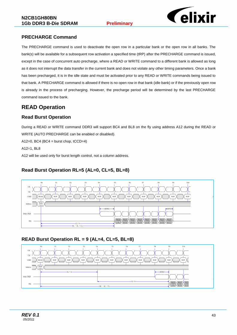
N2CB1GH80BN 1Gb DDR3 B-Die SDRAM Preliminary
REV 0.1 43 05/2011
PRECHARGE Command
The PRECHARGE command is used to deactivate the open row in a particular bank or the open row in all banks. The
bank(s) will be available for a subsequent row activation a specified time (tRP) after the PRECHARGE command is issued,
except in the case of concurrent auto precharge, where a READ or WRITE command to a different bank is allowed as long
as it does not interrupt the data transfer in the current bank and does not violate any other timing parameters. Once a bank
has been precharged, it is in the idle state and must be activated prior to any READ or WRITE commands being issued to
that bank. A PRECHARGE command is allowed if there is no open row in that bank (idle bank) or if the previously open row
is already in the process of precharging. However, the precharge period will be determined by the last PRECHARGE
command issued to the bank.
READ Operation
Read Burst Operation
During a READ or WRITE command DDR3 will support BC4 and BL8 on the fly using address A12 during the READ or
WRITE (AUTO PRECHARGE can be enabled or disabled).
A12=0, BC4 (BC4 = burst chop, tCCD=4)
A12=1, BL8
A12 will be used only for burst length control, not a column address.
Read Burst Operation RL=5 (AL=0, CL=5, BL=8)
READ Burst Operation RL = 9 (AL=4, CL=5, BL=8)
CK
CK
T0 T1 T3 T5 T6 T7 T9 T145
CL=5
DQS, DQS
T2 T4 T8 T10
READ NOPCMD NOP NOP NOP NOP NOP NOP NOP NOP NOP NOP
Bank
Col nAddress
Dout
n
Dout
n +1
Dout
n +2
Dout
n +3
Dout
n +4
Dout
n +5
Dout
n +6
Dout
n +7DQ
RL = AL + CL
tRPRE tRPST
CK
CK
T0 T1 T3 T5 T6 T7 T9 T145
CL=5
DQS, DQS
T2 T4 T8 T10
READ NOPCMD NOP NOP NOP NOP NOP NOP NOP NOP NOP NOP
Bank
Col nAddress
Dout
n
Dout
n +1
Dout
n +2
Dout
n +3
Dout
n +4
Dout
n +5DQ
RL = AL + CL
tRPREAL = 4
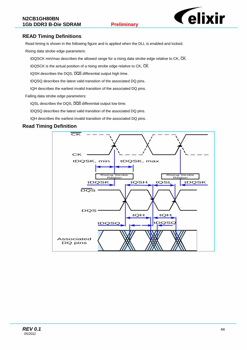
N2CB1GH80BN 1Gb DDR3 B-Die SDRAM Preliminary
REV 0.1 44 05/2011
READ Timing Definitions
Read timing is shown in the following figure and is applied when the DLL is enabled and locked.
Rising data strobe edge parameters:
tDQSCK min/max describes the allowed range for a rising data strobe edge relative to CK, .
tDQSCK is the actual position of a rising strobe edge relative to CK, .
tQSH describes the DQS, differential output high time.
tDQSQ describes the latest valid transition of the associated DQ pins.
tQH describes the earliest invalid transition of the associated DQ pins.
Falling data strobe edge parameters:
tQSL describes the DQS, differential output low time.
tDQSQ describes the latest valid transition of the associated DQ pins.
tQH describes the earliest invalid transition of the associated DQ pins.
Read Timing Definition
Rising Strobe
Region
tDQSK, min tDQSK, max
tDQSK
CK
CK
DQS
DQS
tDQSK
Rising Strobe
Region
tQSH tQSL
tQH tQH
tDQSQ tDQSQ
Associated
DQ pins
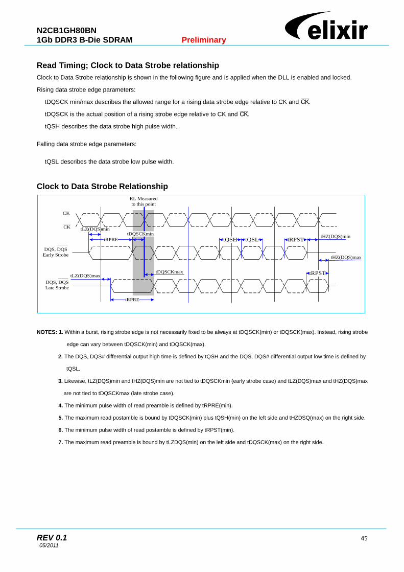
N2CB1GH80BN 1Gb DDR3 B-Die SDRAM Preliminary
REV 0.1 45 05/2011
Read Timing; Clock to Data Strobe relationship
Clock to Data Strobe relationship is shown in the following figure and is applied when the DLL is enabled and locked.
Rising data strobe edge parameters:
tDQSCK min/max describes the allowed range for a rising data strobe edge relative to CK and .
tDQSCK is the actual position of a rising strobe edge relative to CK and .
tQSH describes the data strobe high pulse width.
Falling data strobe edge parameters:
tQSL describes the data strobe low pulse width.
Clock to Data Strobe Relationship
NOTES: 1. Within a burst, rising strobe edge is not necessarily fixed to be always at tDQSCK(min) or tDQSCK(max). Instead, rising strobe
edge can vary between tDQSCK(min) and tDQSCK(max).
2. The DQS, DQS# differential output high time is defined by tQSH and the DQS, DQS# differential output low time is defined by
tQSL.
3. Likewise, tLZ(DQS)min and tHZ(DQS)min are not tied to tDQSCKmin (early strobe case) and tLZ(DQS)max and tHZ(DQS)max
are not tied to tDQSCKmax (late strobe case).
4. The minimum pulse width of read preamble is defined by tRPRE(min).
5. The maximum read postamble is bound by tDQSCK(min) plus tQSH(min) on the left side and tHZDSQ(max) on the right side.
6. The minimum pulse width of read postamble is defined by tRPST(min).
7. The maximum read preamble is bound by tLZDQS(min) on the left side and tDQSCK(max) on the right side.
CK
CK
RL Measured
to this point
DQS, DQS
Early Strobe
DQS, DQS
Late Strobe
tLZ(DQS)min
tLZ(DQS)max
tRPRE
tRPRE
tDQSCKmin
tDQSCKmax
tQSH tQSL tRPST
tRPST
tHZ(DQS)min
tHZ(DQS)max
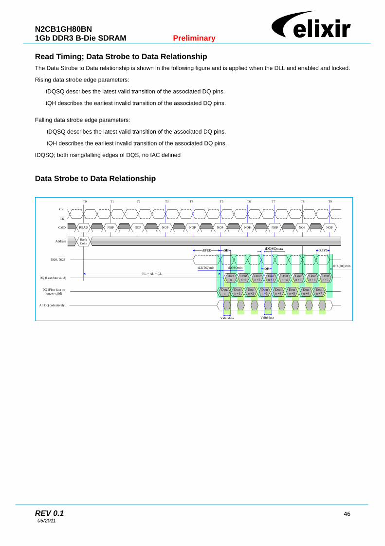
N2CB1GH80BN 1Gb DDR3 B-Die SDRAM Preliminary
REV 0.1 46 05/2011
Read Timing; Data Strobe to Data Relationship
The Data Strobe to Data relationship is shown in the following figure and is applied when the DLL and enabled and locked.
Rising data strobe edge parameters:
tDQSQ describes the latest valid transition of the associated DQ pins.
tQH describes the earliest invalid transition of the associated DQ pins.
Falling data strobe edge parameters:
tDQSQ describes the latest valid transition of the associated DQ pins.
tQH describes the earliest invalid transition of the associated DQ pins.
tDQSQ; both rising/falling edges of DQS, no tAC defined
Data Strobe to Data Relationship
Dout
n +6
Dout
n +7
tRPST
CK
CK
T0 T1 T3 T5 T6 T7 T9
DQS, DQS
T2 T4 T8
READ NOPCMD NOP NOP NOP NOP NOP NOP NOP NOP
Bank
Col nAddress
Dout
n +1
Dout
n +2
Dout
n +3
Dout
n +4
Dout
n +5DQ (Last data valid)
RL = AL + CL
tRPRE
Dout
n +6
Dout
n +7
Dout
n
Dout
n +1
Dout
n +2
Dout
n +3
Dout
n +4
Dout
n +5
tLZ(DQ)min
Valid data
tHZ(DQ)min
tDQSQmax
Valid data
tQH
tQH
Dout
n
tDQSQmin
DQ (First data no
longer valid)
All DQ collectively
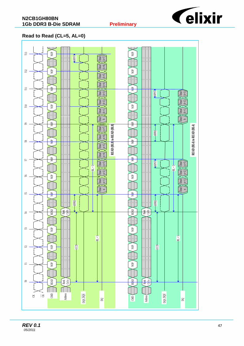
N2CB1GH80BN 1Gb DDR3 B-Die SDRAM Preliminary
REV 0.1 47 05/2011
Read to Read (CL=5, AL=0)
T11
T10
NO
PN
OP
Dou
t
n +6
Dou
t
n +7
tRPS
T
CK CK
T0T1
T3T5
T6T7
T9T2
T4T8
NO
PCM
DN
OP
NO
PRE
AD
NO
PN
OP
NO
PN
OP
NO
P
Add
ress
Dou
t
n +1
Dou
t
n +2
Dou
t
n +3
Dou
t
n +4
Dou
t
n +5
tCCD
tRPR
E
Dou
t
n
T12
NO
P
T13
NO
P
RL =
5
Bank
Col b
REA
D
Dou
t
b +6
Dou
t
b +7
Dou
t
b +1
Dou
t
b +2
Dou
t
b +3
Dou
t
b +4
Dou
t
b +5
Dou
t
b
RL =
5
DQ
S, D
QS
DQ
REA
D (B
L8) t
o R
EAD
(BL8
)
NO
PN
OP
tRPS
T
NO
PCM
DN
OP
NO
PRE
AD
NO
PN
OP
NO
PN
OP
NO
P
Add
ress
Dou
t
n +1
Dou
t
n +2
Dou
t
n +3
tCCD
tRPR
E
Dou
t
n
NO
PN
OP
RL =
5
Bank
Col b
REA
D
Dou
t
b +1
Dou
t
b +2
Dou
t
b +3
Dou
t
b
RL =
5
DQ
S, D
QS
DQ
REA
D (B
L4) t
o R
EAD
(BL4
)
tRPR
EtR
PST
REA
D
Bank
Col n
REA
D
Bank
Col n
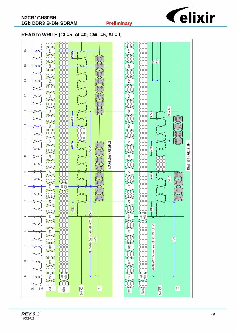
N2CB1GH80BN 1Gb DDR3 B-Die SDRAM Preliminary
REV 0.1 48 05/2011
READ to WRITE (CL=5, AL=0; CWL=5, AL=0)
T11
T10
NOP
Dout
n +6
Dout
n +7
tWPS
T
CK CK
T0T1
T3T5
T6T7
T9T2
T4T8
NOP
CMD
NOP
NOP
WRI
TE
Addr
ess
Dout
n +1
Dout
n +2
Dout
n +3
Dout
n +4
Dout
n +5
READ
to W
rite C
omma
nd de
lay =
RL
+tCC
D +
2tCK
-WLtR
PRE
Dout n
T12
NOP
T13
NOP
RL =
5
Bank
Col b
Dout
b +7
Dout
b +1
Dout
b +2
Dout
b +3
Dout
b +4
Dout
b +5
WL
= 5
DQS,
DQS DQ
READ
(BL8
) to W
RITE
(BL8
)
NOP
tWPS
T
NOP
CMD
NOP
NOP
NOP
Addr
ess
Dout
n +1
Dout
n +2
Dout
n +3
READ
to W
RITE
Com
mand
Dela
y = R
L +
tCCD
/2 +
2tCK
- WL
tRPR
E
Dout n
NOP
NOP
RL =
5
READ
Dout
b +1
Dout
b +2
Dout
b +3
WL
= 5
DQS,
DQS
READ
(BL4
) to W
RITE
(BL4
)
tWPR
EtR
PST
T14
T15
NOP
NOP
tWRP
REtR
PST
Bank
Col n
READ
NOP
NOP
NOP
NOP
NOP
NOP
DQ
NOP
NOP
tBL
= 4 c
locks
tWR
tWTR
READ
Bank
Col n
WRI
TE
Bank
Col b
NOP
Dout b
NOP
NOP
NOP
NOP
Dout b
Dout
b +6
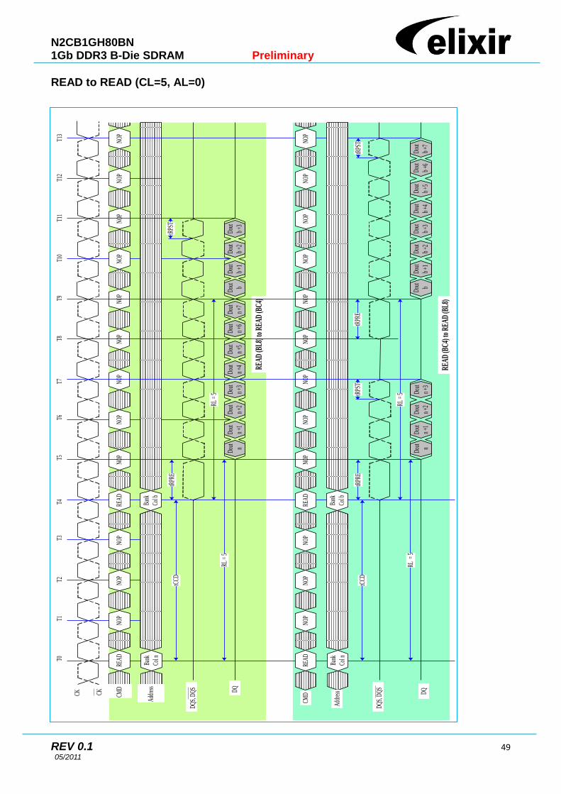
N2CB1GH80BN 1Gb DDR3 B-Die SDRAM Preliminary
REV 0.1 49 05/2011
READ to READ (CL=5, AL=0)
T11
T10
NO
PN
OP
Dou
t
n +6
Dou
t
n +7
tRPS
T
CK CK
T0T1
T3T5
T6T7
T9T2
T4T8
NO
PCM
DN
OP
NO
PN
OP
NO
PN
OP
NO
PN
OP
Add
ress
Dou
t
n +1
Dou
t
n +2
Dou
t
n +3
Dou
t
n +4
Dou
t
n +5
tCCD
tRPR
E
Dou
t
n
T12
NO
P
T13
NO
P
RL =
5
REA
D
Dou
t
b +1
Dou
t
b +2
Dou
t
b +3
Dou
t
b
RL =
5
DQ
S, D
QS DQ
REA
D (B
L8) t
o R
EAD
(BC
4)
NO
PN
OP
tRPS
T
NO
PCM
DN
OP
NO
PN
OP
NO
PN
OP
NO
PN
OP
Add
ress
Dou
t
n +1
Dou
t
n +2
Dou
t
n +3
tCCD
tRPR
E
Dou
t
n
NO
PN
OP
RL =
5
REA
D
RL =
5
DQ
S, D
QS
REA
D (B
C4)
to R
EAD
(BL8
)
tRPR
EtR
PST
DQ
REA
D
Bank
Col n
REA
D
Bank
Col n
REA
D
Bank
Col b
REA
D
Bank
Col b
Dou
t
b +6
Dou
t
b +7
Dou
t
b +1
Dou
t
b +2
Dou
t
b +3
Dou
t
b +4
Dou
t
b +5
Dou
t
b
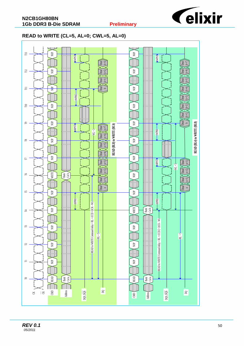
N2CB1GH80BN 1Gb DDR3 B-Die SDRAM Preliminary
REV 0.1 50 05/2011
READ to WRITE (CL=5, AL=0; CWL=5, AL=0)
T11
T10
NOP
NOP
Dou
t
n +6
Dout
n +7
tRPS
T
CK CK
T0T1
T3T5
T6T7
T9T2
T4T8
NOP
CMD
NOP
NOP
WRI
TE
Add
ress
Dout
n +1
Dout
n +2
Dout
n +3
Dout
n +4
Dou
t
n +5
tRPR
E
Dout n
T12
NOP
T13
NOP
RL =
5
READ
Dout
b +1
Dout
b +2
Dou
t
b +3
WL
= 5
DQS,
DQ
S DQ
NOP
NOP
tWPS
T
NOP
CMD
NOP
NOP
NOP
Addr
ess
Dout
n +1
Dout
n +2
Dout
n +3
REA
D to
WRI
TE C
omm
and
dela
y =
RL +
tCCD
/2 +
2tCK
- W
LtR
PRE
Dout n
NOP
NOP
RL =
5
READ
WL
= 5
DQS,
DQ
S
REA
D (B
L4) t
o W
RIT
E (B
L8)
tWPR
EtR
PST
DQ
READ
Bank
Col n
READ
Bank
Col n
NOP
Bank
Col b
WRI
TE
Bank
Col b
Dou
t
b +6
Dout
b +7
Dout
b +1
Dout
b +2
Dout
b +3
Dout
b +4
Dout
b +5
Dout b
NOP
NOP
NOP
NO
P
REA
D (B
L8) t
o W
RIT
E (B
C4)
NOP
NOP
NOP
NO
P
tWPS
TtW
PRE
Dou
t
b
REA
D to
WRI
TE C
omm
and
dela
y =
RL +
tCCD
+2t
CK -
WL

N2CB1GH80BN 1Gb DDR3 B-Die SDRAM Preliminary
REV 0.1 51 05/2011
Write Operation
DDR3 Burst Operation
During a READ or WRITE command, DDR3 will support BC4 and BL8 on the fly using address A12 during the READ or
WRITE (Auto Precharge can be enabled or disabled).
A12=0, BC4 (BC4 = Burst Chop, tCCD=4)
A12=1, BL8
A12 is used only for burst length control, not as a column address.
WRITE Timing Violations
Motivation
Generally, if timing parameters are violated, a complete reset/initialization procedure has to be initiated to make sure the
DRAM works properly. However, it is desirable for certain minor violations that the DRAM is guaranteed not to “hang up”
and errors be limited to that particular operation.
For the following, it will be assumed that there are no timing violations with regard to the Write command itself (including
ODT, etc.) and that it does satisfy all timing requirements not mentioned below.
Data Setup and Hold Violations
Should the strobe timing requirements (tDS, tDH) be violated, for any of the strobe edges associated with a write burst, then
wrong data might be written to the memory location addressed with the offending WRITE command.
Subsequent reads from that location might result in unpredictable read data, however, the DRAM will work properly
otherwise.
Strobe to Strobe and Strobe to Clock Violations
Should the strobe timing requirements (tDQSH, tDQSL, tWPRE, tWPST) or the strobe to clock timing requirements (tDSS,
tDSH, tDQSS) be violated, for any of the strobe edges associated with a Write burst, then wrong data might be written to
the memory location addressed with the offending WRITE command. Subsequent reads from that location might result in
unpredictable read data, however the DRAM will work properly otherwise.
Write Timing Parameters
This drawing is for example only to enumerate the strobe edges that “belong” to a write burst. No actual timing violations
are shown here. For a valid burst all timing parameters for each edge of a burst need to be satisfied (not only for one edge -
as shown).

N2CB1GH80BN 1Gb DDR3 B-Die SDRAM Preliminary
REV 0.1 52 05/2011
Write Timing Definition
Note:
1. BL=8, WL=5 (AL=0, CWL=5).
2. Din n = data in from column n.
3. NOP commands are shown for ease of illustration; other command may be valid at these times.
4. BL8 setting activated by either MR0 [A1:0=00] or MR0 [A1:0=01] and A12 = 1 during WRITE command at T0.
5. tDQSS must be met at each rising clock edge.
Tn
CK
CK
T0 T1 T3 T5 T6 T7 T9T2 T4 T8
NOPCMD NOP NOP
Address
DQ
NOP
WL = AL + CWL
NOP NOP
Din
n +6
Din
n +7
Din
n +1
Din
n +2
Din
n +3
Din
n +4
Din
n +5
Din
n
tDQSS tDSH
tDQSL
tDSS
tWPST(min)
tDQSL(min)
tDSStDSS tDSS
tDSS
DQ
tDSH
tDQSH tDQSL
tDSS
tDQSH
tWPRE(min)
tDSS
tDSH
tDQSH
tDSHtDSH
tDSS tDSS
tDSS
DQ Din
n +6
Din
n +7
Din
n +1
Din
n +2
Din
n +3
Din
n +4
Din
n +5
Din
n
tDSH
tDQSH tDQSH
tDSH
tDQSH
tDSHtDSH
NOP
tDQSH
tWPRE(min)
Write
Bank
Col n
tWPRE(min)
tDQSH
NOP
tDSS
tDQSLtDSS tDSS
NOP
tDSHtDSH
Din
n +6
Din
n +7
Din
n +1
Din
n +2
Din
n +3
Din
n +4
Din
n +5
Din
n
tDQSH
tDSH
NOP
tDSS
tDSS
tDQSL(min)
tWPST(min)
tDQSL(min)
tWPST(min)
tDQSS
DQS, DQS
(tDQSS min)
DQS, DQS
(tDQSS nominal)
DQS, DQS
(tDQSS max)

N2CB1GH80BN 1Gb DDR3 B-Die SDRAM Preliminary
REV 0.1 53 05/2011
WRITE to WRITE (WL=5; CWL=5, AL=0)
T11
T10
NO
P
Dou
t
n +7
CK CK
T0T1
T3T5
T6T7
T9T2
T4T8
NO
PCM
DN
OP
NOP
NO
P
Add
ress
Dou
t
n +1
Dou
t
n +2
Dou
t
n +3
Dout
n +5
tCCD
tWPR
E
T12
NO
P
T13
NOP
WL
= 5
Dou
t
b +6
Dou
t
b +7
Dou
t
b +1
Dou
t
b +2
Dout
b +3
Dou
t
b +5
WL
= 5
DQ
S, D
QS
DQ
WR
ITE
(BL8
) to
WR
ITE
(BL8
)
NO
P
tWPS
T
NO
PCM
DN
OP
NOP
NO
P
Add
ress
Dou
t
n +1
Dou
t
n +2
Dou
t
n +3
tCCD
tRPR
E
NO
PNO
P
WL
= 5
REA
D
Dout
b +1
Dou
t
b +2
Dou
t
b +3
WL
= 5
DQ
S, D
QS
WR
ITE
(BC
4) to
WR
ITE
(BC
4)
tWPR
EtW
PST
tWPS
T
Bank
Col n
WRI
TEN
OPNO
PNO
PN
OP
NOP
WRI
TE
DQ
WRI
TE
Bank
Col n
WRI
TE
Bank
Col b
NOP
Bank
Col b
Dout n
NO
PN
OPNO
PNO
P
Dout
n +4
Dou
t
n +6
Dou
t
b
Dout
b +4
tBL=
4
tWR
tWTR
tBL=
4
tWR
tWTR
Dou
t
n
Dou
t
b

N2CB1GH80BN 1Gb DDR3 B-Die SDRAM Preliminary
REV 0.1 54 05/2011
WRITE to READ (RL=5, CL=5, AL=0; WL=5, CWL=5, AL=0; BL=4)
T11
T10
NO
P
Dou
t
n +7
CK CK
T0T1
T3T5
T6T7
T9T2
T4T8
NO
PCM
DN
OP
NO
PN
OP
Add
ress
Dou
t
n +1
Dou
t
n +2
Dou
t
n +3
Dou
t
n +5
tWPR
E
T12
NO
P
T13
REA
D
WL
= 5
DQ
S, D
QS
DQ
WR
ITE
(BL8
) to
REA
D (B
C4/
BL8)
NO
PN
OP
CMD
NO
PN
OP
NO
P
Add
ress
Dou
t
n +1
Dou
t
n +2
Dou
t
n +3
tRPR
E
Dou
t
n
NO
PRE
AD
WL
= 5
DQ
S, D
QS
WR
ITE
(BC
4) to
REA
D (B
C4/
BL8)
tWPS
T
Bank
Col n
WRI
TEN
OP
NO
PN
OP
NO
PN
OP
NO
P
DQ
WRI
TE
Bank
Col n
NO
PN
OP
Bank
Col b
Dou
t
n
NO
PN
OP
NO
PN
OP
Dou
t
n +4
Dou
t
n +6
tWTR
RL=5
tBL=
4
tWPS
T
Bank
Col b
tWTR
RL=5
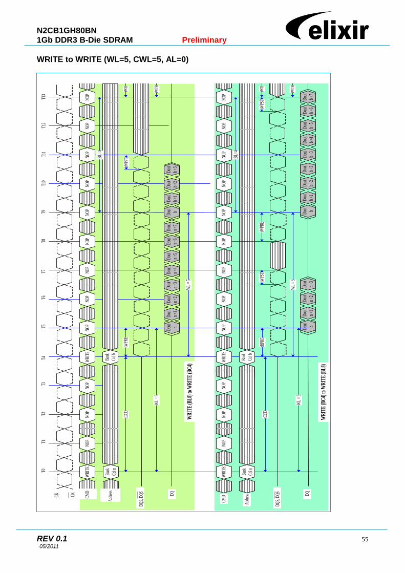
N2CB1GH80BN 1Gb DDR3 B-Die SDRAM Preliminary
REV 0.1 55 05/2011
WRITE to WRITE (WL=5, CWL=5, AL=0)
T11
T10
NO
P
Dou
t
n +7
CK CK
T0T1
T3T5
T6T7
T9T2
T4T8
NO
PCM
DN
OPN
OPNO
P
Addr
ess
Dou
t
n +1
Dout
n +2
Dou
t
n +3
Dout
n +5
tCCD
tWPR
E
T12
NOP
T13
NOP
WL
= 5
Dou
t
b +1
Dou
t
b +2
WL
= 5
DQS,
DQS D
Q
WR
ITE
(BL8
) to
WR
ITE
(BC
4)
NO
P
tWPS
T
NO
PCM
DN
OPN
OPNO
P
Add
ress
Dout
n +1
Dout
n +2
Dou
t
n +3
tCCD
tRPR
E
Dout n
NOP
NOP
WL
= 5
READ
Dout
b +1
Dout
b +2
Dou
t
b +3
WL
= 5
DQS,
DQS
WR
ITE
(BC
4) to
WR
ITE
(BL8
)
tWPR
EtW
PST
tWPS
T
Bank
Col n
WRI
TEN
OPNO
PNO
PN
OP
NOP
WRI
TE
DQ
WRI
TE
Bank
Col n
WRI
TE
Bank
Col b
NOP
Bank
Col b
Dout n
NO
PN
OPNO
PNO
P
Dout
n +4
Dou
t
n +6
Dout b
tBL=
4
tWR
tWTR
tBL=
4
tWR
tWTR
Dout
b +3
Dout
b +6
Dout
b +7
Dout
b +3
Dou
t
b +5
Dout
b +4
Dout b

N2CB1GH80BN 1Gb DDR3 B-Die SDRAM Preliminary
REV 0.1 56 05/2011
Refresh Command
The Refresh command (REF) is used during normal operation of the DDR3 SDRAMs. This command is not persistent, so it
must be issued each time a refresh is required. The DDR3 SDRAM requires Refresh cycles at an average periodic interval
of tREFI. When , , and are held Low and High at the rising edge of the clock, the chip enters a Refresh
cycle. All banks of the SDRAM must be precharged and idle for a minimum of the precharge time tRP(min) before the
Refresh Command can be applied. The refresh addressing is generated by the internal refresh controller. This makes the
address bits “Don‟t Care” during a Refresh command. An internal address counter suppliers the address during the refresh
cycle. No control of the external address bus is required once this cycle has started. When the refresh cycle has completed,
all banks of the SDRAM will be in the precharged (idle) state. A delay between the Refresh Command and the next valid
command, except NOP or DES, must be greater than or equal to the minimum Refresh cycle time tRFC(min) as shown in
the following figure.
In general, a Refresh command needs to be issued to the DDR3 SDRAM regularly every tREFI interval. To allow for
improved efficiency in scheduling and switching between tasks, some flexibility in the absolute refresh interval is provided.
A maximum of 8 Refresh commands can be postponed during operation of the DDR3 SDRAM, meaning that at no point in
time more than a total of 8 Refresh commands are allowed to be postponed. In case that 8 Refresh commands are
postponed in a row, the resulting maximum interval between the surrounding Refresh commands is limited to 9 x tREFI. A
maximum of 8 additional Refresh commands can be issued in advance (“pulled in”), with each one reducing the number of
regular Refresh commands required later by one. Note that pulling in more than 8 Refresh commands in advance does not
further reduce the number of regular Refresh commands required later, so that the resulting maximum interval between two
surrounding Refresh command is limited to 9 x tREFI. Before entering Self-Refresh Mode, all postponed Refresh
commands must be executed.
Self-Refresh Entry/Exit Timing
Postponing Refresh Commands (Example)
CK
CK
T0 T1 Ta0 Tb0 Tb1 Tb3Ta1 Tb2
NOPCMD NOP REF ValidNOPREF NOP Valid ValidValid Valid REF
Tc0 Tc1
Valid
tRFC tRFC(min)
tREFI (max, 9 x tREFI)DRAM must be idle
DRAM must be idle
Time Break
9 x tREFI
tREFI
tREFI
8 REF-Command postponed
t
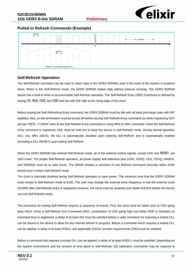
N2CB1GH80BN 1Gb DDR3 B-Die SDRAM Preliminary
REV 0.1 57 05/2011
Pulled-in Refresh Commands (Example)
Self-Refresh Operation
The Self-Refresh command can be used to retain data in the DDR3 SDRAM, even if the reset of the system is powered
down. When in the Self-Refresh mode, the DDR3 SDRAM retains data without external clocking. The DDR3 SDRAM
device has a built-in timer to accommodate Self-Refresh operation. The Self-Refresh Entry (SRE) Command is defined by
having , , , and held low with WE high at the rising edge of the clock.
Before issuing the Self-Refreshing-Entry command, the DDR3 SDRAM must be idle with all bank precharge state with tRP
satisfied. Also, on-die termination must be turned off before issuing Self-Refresh-Entry command, by either registering ODT
pin low “ODTL + 0.5tCK” prior to the Self-Refresh Entry command or using MRS to MR1 command. Once the Self-Refresh
Entry command is registered, CKE must be held low to keep the device in Self-Refresh mode. During normal operation
(DLL on), MR1 (A0=0), the DLL is automatically disabled upon entering Self-Refresh and is automatically enabled
(including a DLL-RESET) upon exiting Self-Refresh.
When the DDR3 SDRAM has entered Self-Refresh mode, all of the external control signals, except CKE and , are
“don‟t care”. For proper Self-Refresh operation, all power supply and reference pins (VDD, VDDQ, VSS, VSSQ, VRefCA,
and VRefDQ) must be at valid levels. The DRAM initiates a minimum of one Refresh command internally within tCKE
period once it enters Self-Refresh mode.
The clock is internally disabled during Self-Refresh operation to save power. The minimum time that the DDR3 SDRAM
must remain in Self-Refresh mode is tCKE. The user may change the external clock frequency or halt the external clock
tCKSRE after Self-Refresh entry is registered; however, the clock must be restarted and stable tCKSRX before the device
can exit Self-Refresh mode.
The procedure for exiting Self-Refresh requires a sequence of events. First, the clock must be stable prior to CKE going
back HIGH. Once a Self-Refresh Exit Command (SRX, combination of CKE going high and either NOP or Deselect on
command bus) is registered, a delay of at least tXS must be satisfied before a valid command not requiring a locked DLL
can be issued to the device to allow for any internal refresh in progress. Before a command which requires a locked DLL
can be applied, a delay of at least tXSDLL and applicable ZQCAL function requirements [TBD] must be satisfied.
Before a command that requires a locked DLL can be applied, a delay of at least tXSDLL must be satisfied. Depending on
the system environment and the amount of time spent in Self-Refresh, ZQ calibration commands may be required to
9 x tREFI
tREFI
t
tREFI
8 REF-Commands pulled-in

N2CB1GH80BN 1Gb DDR3 B-Die SDRAM Preliminary
REV 0.1 58 05/2011
compensate for the voltage and temperature drift as described in “ZQ Calibration Commands”. To issue ZQ calibration
commands, applicable timing requirements must be satisfied.
CKE must remain HIGH for the entire Self-Refresh exit period tXSDLL for proper operation except for Self-Refresh re-entry.
Upon exit from Self-Refresh, the DDR3 SDRAM can be put back into Self-Refresh mode after waiting at least tXS period
and issuing one refresh command (refresh period of tRFC). NOP or deselect commands must be registered on each
positive clock edge during the Self-Refresh exit interval tXS. ODT must be turned off during tXSDLL.
The use of Self-Refresh mode instructs the possibility that an internally times refresh event can be missed when CKE is
raised for exit from Self-Refresh mode. Upon exit from Self-Refresh, the DDR3 SDRAM requires a minimum of one extra
refresh command before it is put back into Self-Refresh mode.
Self-Refresh Entry/Exit Timing
CK, CK
T1 T2 Ta0 Tb0 Tc0 Tc1 Te0 Tf
ODTL
tCKSRE tCKSRX
tCPDED
tRF
SRE NOP Valid 2)
tCKESR
tXSDLL
tXS
CMD
ODT
Note:
1. Only NOP or DES commands
2. Valid commands not requiring a locked DLL
3. Valid commands requiring a locked DLL
T0 Td0
ValidCKE
NOP SRX NOP 1) Valid 3)
Valid Valid
Valid
Valid
Enter Self Refresh Exit Self Refresh
Do Not
Care
Time
Break
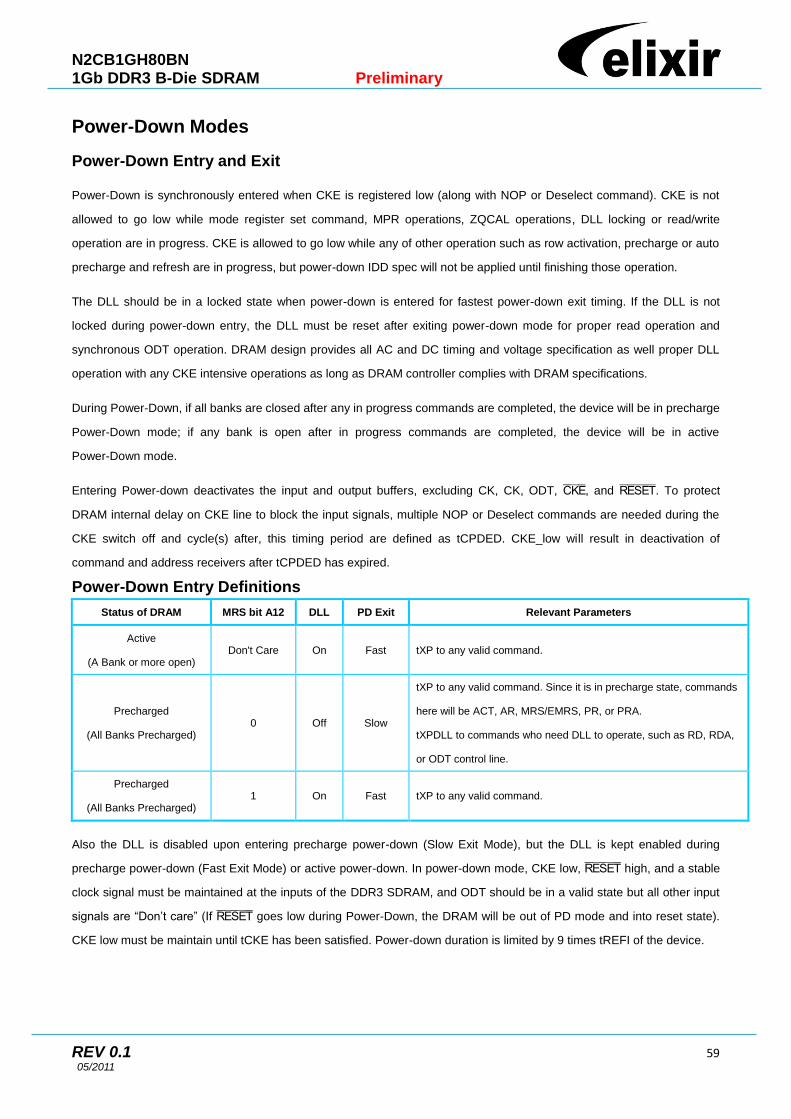
N2CB1GH80BN 1Gb DDR3 B-Die SDRAM Preliminary
REV 0.1 59 05/2011
Power-Down Modes
Power-Down Entry and Exit
Power-Down is synchronously entered when CKE is registered low (along with NOP or Deselect command). CKE is not
allowed to go low while mode register set command, MPR operations, ZQCAL operations, DLL locking or read/write
operation are in progress. CKE is allowed to go low while any of other operation such as row activation, precharge or auto
precharge and refresh are in progress, but power-down IDD spec will not be applied until finishing those operation.
The DLL should be in a locked state when power-down is entered for fastest power-down exit timing. If the DLL is not
locked during power-down entry, the DLL must be reset after exiting power-down mode for proper read operation and
synchronous ODT operation. DRAM design provides all AC and DC timing and voltage specification as well proper DLL
operation with any CKE intensive operations as long as DRAM controller complies with DRAM specifications.
During Power-Down, if all banks are closed after any in progress commands are completed, the device will be in precharge
Power-Down mode; if any bank is open after in progress commands are completed, the device will be in active
Power-Down mode.
Entering Power-down deactivates the input and output buffers, excluding CK, CK, ODT, , and . To protect
DRAM internal delay on CKE line to block the input signals, multiple NOP or Deselect commands are needed during the
CKE switch off and cycle(s) after, this timing period are defined as tCPDED. CKE_low will result in deactivation of
command and address receivers after tCPDED has expired.
Power-Down Entry Definitions
Status of DRAM MRS bit A12 DLL PD Exit Relevant Parameters
Active
(A Bank or more open) Don't Care On Fast tXP to any valid command.
Precharged
(All Banks Precharged) 0 Off Slow
tXP to any valid command. Since it is in precharge state, commands
here will be ACT, AR, MRS/EMRS, PR, or PRA.
tXPDLL to commands who need DLL to operate, such as RD, RDA,
or ODT control line.
Precharged
(All Banks Precharged) 1 On Fast tXP to any valid command.
Also the DLL is disabled upon entering precharge power-down (Slow Exit Mode), but the DLL is kept enabled during
precharge power-down (Fast Exit Mode) or active power-down. In power-down mode, CKE low, high, and a stable
clock signal must be maintained at the inputs of the DDR3 SDRAM, and ODT should be in a valid state but all other input
signals are “Don‟t care” (If goes low during Power-Down, the DRAM will be out of PD mode and into reset state).
CKE low must be maintain until tCKE has been satisfied. Power-down duration is limited by 9 times tREFI of the device.

N2CB1GH80BN 1Gb DDR3 B-Die SDRAM Preliminary
REV 0.1 60 05/2011
The power-down state is synchronously exited when CKE is registered high (along with a NOP or Deselect command).
CKE high must be maintained until tCKE has been satisfied. A valid, executable command can be applied with power-down
exit latency, tXP and/or tXPDLL after CKE goes high. Power-down exit latency is defined at AC spec table of this datasheet.
Active Power-Down Entry and Exit timing diagram
Timing Diagrams for CKE with PD Entry, PD Exit with Read, READ with Auto Precharge, Write and Write with Auto
Precharge, Activate, Precharge, Refresh, MRS:
Power-Down Entry after Read and Read with Auto Precharge
Precharge Power-Down (Fast Exit Mode) Entry and Exit
T0 T1 T2 Ta0 Ta1 Tb0 Tb1 Tc0
CK
CK
Valid NOP NOP NOP NOP NOP NOPCMD
CKEValid Valid
tIS
tIH
tPDtIH
tIS tCKE
Address Valid Valid
tCPDED
Enter
Power-DownExit
Power-Down
tXP
Do not
care
Time
Break
T0 T1 Ta0 Ta1 Ta2 Ta3 Ta4 Ta5
CK
CK
WRITE NOP NOP NOP NOP NOP NOPCMD
CKE
AddressBank,
Col n
Power-Down
Entry Do not
care
Time
Break
Ta6 Ta7 Tb0 Tb1 Tb2
NOP NOP NOP NOP NOP NOP
tIStCPDED
DQS
WL=AL+CWL
Din
b
Din
b+1
Din
b+2
Din
b+3
Din
b+4
Din
b+5
Din
b+6
Din
b+7
Din
b
Din
b+1
Din
b+2
Din
b+3
tWRAPDEN
BL8
BC4
WR (1)
Tb3
NOP
Tc0
Valid
tPD
Start Internal
Precharge
T0 T1 T2 Ta0 Ta1 Tb0 Tb1 Tc0
CK
CK
WRITE NOP NOP NOP NOP NOP NOPCMD
CKE
Do not
care
Time
Break
NOP
tIS
tCPDED
tIH
tCKE
tIS
tXP
NOP Valid
tPD
Enter
Power-Down
Mode
Exit
Power-Down
Mode

N2CB1GH80BN 1Gb DDR3 B-Die SDRAM Preliminary
REV 0.1 61 05/2011
Precharge Power-Down (Slow Exit Mode) Entry and Exit
Refresh Command to Power-Down Entry
T0 T1 T2 Ta0 Ta1 Tb0 Tb1 Tc0
CK
CK
WRITE NOP NOP NOP NOP NOP ValidCMD
CKE
Do not
care
Time
Break
NOP
tIS
tCPDED
tIH
tCKE
tIS
tXP
NOP Valid
tPD
Enter
Power-Down
Mode
Exit
Power-Down
Mode
Td0
Valid
tXPDLL
Valid
T0 T1 T2 T3 Ta0 Ta1
CK
CK
REF NOP NOP ValidCMD
CKE
Do not
care
Time
Break
NOP
tIStCPDED
Valid
tPD
Valid Valid
tREFPDEN
Address
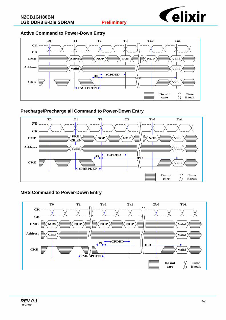
N2CB1GH80BN 1Gb DDR3 B-Die SDRAM Preliminary
REV 0.1 62 05/2011
Active Command to Power-Down Entry
Precharge/Precharge all Command to Power-Down Entry
MRS Command to Power-Down Entry
T0 T1 T2 T3 Ta0 Ta1
CK
CK
Active NOP NOP ValidCMD
CKE
Do not
care
Time
Break
NOP
tIStCPDED
Valid
tPD
Valid Valid
tACTPDEN
Address
T0 T1 T2 T3 Ta0 Ta1
CK
CK
PRE
PREANOP NOP ValidCMD
CKE
Do not
care
Time
Break
NOP
tIStCPDED
Valid
tPD
Valid Valid
tPREPDEN
Address
T0 T1 Ta0 Ta1 Tb0 Tb1
CK
CK
NOP NOP ValidCMD
CKE
Do not
care
Time
Break
NOP
tIStCPDED
Valid
tPD
Valid
tMRSPDEN
Address
MRS
Valid

N2CB1GH80BN 1Gb DDR3 B-Die SDRAM Preliminary
REV 0.1 63 05/2011
On-Die Termination (ODT)
ODT (On-Die Termination) is a feature of the DDR3 SDRAM that allows the DRAM to turn on/off termination resistance for
each DQ, DQS, , and DM for x8 configuration and TDQS, for x8 configuration, when enabled via A11=1 in MR1)
via the ODT control pin. The ODT feature is designed to improve signal integrity of the memory channel by allowing the
DRAM controller to independently turn on/off termination resistance for any or all DRAM devices.
The ODT feature is turned off and not supported in Self-Refresh mode.
A simple functional representation of the DRAM ODT feature is shown as below.
Functional Representation of ODT
The switch is enabled by the internal ODT control logic, which uses the external ODT pin and other control information. The
value of RTT is determined by the settings of Mode Register bits. The ODT pin will be ignored if the Mode Register MR1
and MR2 are programmed to disable ODT and in self-refresh mode.
ODT Mode Register and ODT Truth Table
The ODT Mode is enabled if either of MR1 A2, A6, A9 or MR2 A9, A10 are non-zero. In this case, the value of RTT is
determined by the settings of those bits.
Application: Controller sends WR command together with ODT asserted.
One possible application: The rank that is being written to provides termination.
DRAM turns ON termination if it sees ODT asserted (except ODT is disabled by MR)
DRAM does not use any write or read command decode information.
Termination Truth Table
ODT pin DRAM Termination State
0 OFF
1 ON, (OFF, if disabled by MR1 A2, A6, A9 and MR2A9, A10 in general)
To other
circuitry
like
RCV, ...
VDDQ / 2
RTT
Switch
DQ , DQS, DM, TDQS
ODT

N2CB1GH80BN 1Gb DDR3 B-Die SDRAM Preliminary
REV 0.1 64 05/2011
Synchronous ODT Mode
Synchronous ODT mode is selected whenever the DLL is turned on and locked. Based on the power-down definition, these
modes are:
Any bank active with CKE high
Refresh with CKE high
Idle mode with CKE high
Active power down mode (regardless of MR0 bit A12)
Precharge power down mode if DLL is enabled during precharge power down by MR0 bit A12
The direct ODT feature is not supported during DLL-off mode. The on-die termination resistors must be disabled by continu-
ously registering the ODT pin low and/or by programming the RTT_Nom bits MR1A9,A6,A2 to 0,0,0 via a mode register
set command during DLL-off mode.
In synchronous ODT mode, RTT will be turned on ODTLon clock cycles after ODT is sampled high by a rising clock edge
and turned off ODTLoff clock cycles after ODT is registered low by a rising clock edge. The ODT latency is tied to the write
latency (WL) by: ODTLonn = WL - 2; ODTLoff = WL-2.
ODT Latency and Posted ODT
In synchronous ODT Mode, the Additive Latency (AL) programmed into the Mode Register (MR1) also applies to the ODT
signal. The DRAM internal ODT signal is delayed for a number of clock cycles defined by the Additive Latency (AL) relative
to the external ODT signal. ODTLon = CWL + AL - 2; ODTLoff = CWL + AL - 2. For details, refer to DDR3 SDRAM latency
definitions.
N2CB1GH80BN 1Gb DDR3 B-Die SDRAM Preliminary
REV 0.1 65 05/2011
Timing Parameters
In synchronous ODT mode, the following timing parameters apply: ODTLon, ODTLoff, tAON min/max, tAOF min/max.
Minimum RTT turn-on time (tAON min) is the point in time when the device leaves high impedance and ODT resistance
begins to turn on. Maximum RTT turn-on time (tAON max) is the point in time when the ODT resistance is fully on. Both are
measured from ODTLon.
Minimum RTT turn-off time (tAOF min) is the point in time when the device starts to turn off the ODT resistance. Maximum
RTT turn off time (tAOF max) is the point in time when the on-die termination has reached high impedance. Both are
measured from ODTLoff.
When ODT is asserted, it must remain high until ODTH4 is satisfied. If a Write command is registered by the SDRAM with
ODT high, then ODT must remain high until ODTH4 (BL=4) or ODTH8 (BL=8) after the write command. ODTH4 and
ODTH8 are measured from ODT registered high to ODT registered low or from the registration of a write command until
ODT is registered low.
Synchronous ODT Timing Example for AL=3; CWL=5; ODTLon=AL+CWL-2=6;
ODTLoff=AL+CWL-2=6
Synchronous ODT example with BL=4, WL=7
ODT must be held for at least ODTH4 after assertion (T1); ODT must be kept high ODTH4 (BL=4) or ODTH8
(BL=8) after Write command (T7). ODTH is measured from ODT first registered high to ODT first registered
low, or from registration of Write command with ODT high to ODT registered low. Note that although ODTH4 is
satisfied from ODT registered at T6 ODT must not go low before T11 as ODTH4 must also be satisfied from
the registration of the Write command at T7.
CK
CK
AL=3
T11T10T0 T1 T3 T5 T6 T7 T9T2 T4 T8 T12
ODT
ODTH4, min
ODTLon = CWL + AL -2ODTLoff = CWL + AL -2
T13 T14 T15
CWL - 2
DRAM_RTT
tAONmin
tAONmaxtAONmin
tAONmax
RTT_NOM
AL=3
Transitioning Do not care
CKE
CK
CK
ODTH4
T11T10T0 T1 T3 T5 T6 T7 T9T2 T4 T8 T12
ODT
ODTLon = CWL -2
T13 T14 T15
ODTLoff = WL - 2
DRAM_RTT
tAONmin tAONmax
tAOFmax
RTT_NOM
T16 T17 T18
ODTH4min
ODTH4
ODTLoff = CWL -2
ODTLon = CWL -2
tAOFmin
tAOFmax tAONmax
tAONmintAOFmin
NOP NOP NOP NOP NOP NOP NOP WRS4 NOP NOP NOP NOP NOP NOP NOP NOP NOP NOP NOP
Transitioning Do not care

N2CB1GH80BN 1Gb DDR3 B-Die SDRAM Preliminary
REV 0.1 66 05/2011
ODT during Reads:
As the DDR3 SDRAM cannot terminate and drive at the same time, RTT must be disabled at least half a clock cycle before
the read preamble by driving the ODT pin low appropriately. RTT may not be enabled until the end of the post-amble as
shown in the following figure. DRAM turns on the termination when it stops driving which is determined by tHZ. If DRAM
stops driving early (i.e. tHZ is early), then tAONmin time may apply. If DRAM stops driving late (i.e. tHZ is late), then DRAM
complies with tAONmax timing. Note that ODT may be disabled earlier before the Read and enabled later after the Read
than shown in this example.
ODT must be disabled externally during Reads by driving ODT low. (Example: CL=6;
AL=CL-1=5; RL=AL+CL=11; CWL=5; ODTLon=CWL+AL-2=8; ODTLoff=CWL+AL-2=8)
Dynamic ODT
In certain application cases and to further enhance signal integrity on the data bus, it is desirable that the termination
strength of the DDR3 SDRAM can be changed without issuing an MRS command. This requirement is supported by the
“Dynamic ODT” feature as described as follows:
Functional Description
The Dynamic ODT Mode is enabled if bit (A9) or (A10) of MR2 is set to „1‟. The function is described as follows:
Two RTT values are available: RTT_Nom and RTT_WR.
The value for RTT_Nom is preselected via bits A[9,6,2] in MR1.
The value for RTT_WR is preselected via bits A[10,9] in MR2.
During operation without write commands, the termination is controlled as follows:
Nominal termination strength RTT_Nom is selected.
Termination on/off timing is controlled via ODT pin and latencies ODTLon and ODTLoff.
When a Write command (WR, WRA, WRS4, WRS8, WRAS4, WRAS8) is registered, and if Dynamic ODT is enabled, the
termination is controlled as follows:
A latency ODTLcnw after the write command, termination strength RTT_WR is selected.
A latency ODTLcwn8 (for BL8, fixed by MRS or selected OTF) or ODTLcwn4 (for BC4, fixed by MRS or selected OTF)
after the write command, termination strength RTT_Nom is selected.
CK
CK
T11T10T0 T1 T3 T5 T6 T7 T9T2 T4 T8 T12 T13 T14 T15 T16
CMD
Address
RL = AL + CL
RTT_NOMRTT
ODTLoff = CWL + AL - 2
tAOFmax
tAOFmin
ODTLon = CWL + AL - 2
RTT_NOM
tAONmax
ODT
DRAM
ODT
DQSdiff
Din
b
Din
b+1
Din
b+2
Din
b+3
Din
b+4
Din
b+5
Din
b+6
Din
b+7DQ
Read NOP NOP NOP NOP NOP NOPNOP NOP NOP NOP NOP NOP NOP NOP NOP NOP
Valid
N2CB1GH80BN 1Gb DDR3 B-Die SDRAM Preliminary
REV 0.1 67 05/2011
Termination on/off timing is controlled via ODT pin and ODTLon, ODTLoff.
The following table shows latencies and timing parameters which are relevant for the on-die termination control in Dynamic
ODT mode.
The dynamic ODT feature is not supported at DLL-off mode. User must use MRS command to set RTT_WR, MR2[A10,A9
= [0,0], to disable Dynamic ODT externally.
When ODT is asserted, it must remain high until ODTH4 is satisfied. If a Write command is registered by the SDRAM with
ODT high, then ODT must remain high until ODTH4 (BL=4) or ODTH8 (BL=8) after the Write command. ODTH4 and
ODTH8 are measured from ODT registered high to ODT registered low or from the registration of Write command until ODT
is register low.
Latencies and timing parameters relevant for Dynamic ODT Name and Description
Abbr. Defined from Defined to Definition for all DDR3 speed pin
Unit
ODT turn-on Latency
ODTLon registering external ODT signal high
turning termination on
ODTLon=WL-2 tCK
ODT turn-off Latency
ODTLoff registering external ODT signal low
turning termination off
ODTLoff=WL-2 tCK
ODT Latency for changing from RTT_Nom to RTT_WR
ODTLcnw registering external write command
change RTT strength from RTT_Nom to RTT_WR
ODTLcnw=WL-2 tCK
ODT Latency for change from RTT_WR to RTT_Nom (BL=4)
ODTLcwn4 registering external write command
change RTT strength from RTT_WR to RTT_Nom
ODTLcwn4=4+ODTLoff tCK
ODT Latency for change from RTT_WR to RTT_Nom (BL=8)
ODTLcwn8 registering external write command
change RTT strength from RTT_WR to RTT_Nom
ODTLcwn8=6+ODTLoff tCK(avg)
Minimum ODT high time after ODT assertion
ODTH4 registering ODT high ODT registered low
ODTH4=4 tCK(avg)
Minimum ODT high time after Write (BL=4)
ODTH4 registering write with ODT high
ODT registered low
ODTH4=4 tCK(avg)
Minimum ODT high time after Write (BL=8)
ODTH8 registering write with ODT high
ODT register low ODTH8=6 tCK(avg)
RTT change skew tADC ODTLcnw ODTLcwn
RTT valid tADC(min)=0.3tCK(avg) tADC(max)=0.7tCK(avg)
tCK(avg)
Note: tAOF,nom and tADC,nom are 0.5tCK (effectively adding half a clock cycle to ODTLoff, ODTcnw, and ODTLcwn)

N2CB1GH80BN 1Gb DDR3 B-Die SDRAM Preliminary
REV 0.1 68 05/2011
ODT Timing Diagrams
Dynamic ODT: Behavior with ODT being asserted before and after the write
Note: Example for BC4 (via MRS or OTF), AL=0, CWL=5. ODTH4 applies to first registering ODT high and to the registration of the Write
command. In this example ODTH4 would be satisfied if ODT went low at T8. (4 clocks after the Write command).
Dynamic ODT: Behavior without write command, AL=0, CWL=5
Note: ODTH4 is defined from ODT registered high to ODT registered low, so in this example ODTH4 is satisfied; ODT registered low at T5
would also be legal.
CK
CK
T11T10T0 T1 T3 T5 T6 T7 T9T2 T4 T8 T12 T13 T14 T15 T16
CMD
ODT
RTT
DQS/DQS
DQ
ODTLon
ODTLcwn4
T17
ODTLcnw
tAONmin
tAONmax
tADCmin
tADCmax
WL
tADCmin
tADCmax
tAOFmin
tAOFmax
Address
RTT_WR
Din
n
Din
n+1
Din
n+2
Din
n+3
ODTH4 ODTLoff
NOP NOP NOP NOP WRS4 NOP NOP NOP NOP NOP NOP NOP NOP NOP NOP NOP NOP NOP
Valid
ODTH4
RTT_Nom
Do not
careTransitioning
RTT_Nom
tADCmax
CK
CK
T11T10T0 T1 T3 T5 T6 T7 T9T2 T4 T8
CMD
ODT
RTT
DQS/DQS
DQ
ODTLon
ODTLoff
tAONmin
tAONmax
tADCmin
RTT_Nom
Valid Valid Valid Valid Valid Valid Valid Valid Valid Valid Valid Valid
Address
ODTH4 ODTLoff
Do not
careTransitioning

N2CB1GH80BN 1Gb DDR3 B-Die SDRAM Preliminary
REV 0.1 69 05/2011
Dynamic ODT: Behavior with ODT pin being asserted together with write command
for the duration of 6 clock cycles.
Note: Example for BL8 (via MRS or OTF), AL=0, CWL=5. In this example ODTH8=6 is exactly satisfied.
Dynamic ODT: Behavior with ODT pin being asserted together with write
command for a duration of 6 clock cycles, example for BC4 (via MRS or OTF),
AL=0, CWL=5.
tAOFmax
tAOFmin
CK
CK
T11T10T0 T1 T3 T5 T6 T7 T9T2 T4 T8
CMD
ODT
RTT
DQS/DQS
DQ
ODTH8
ODTLon
ODTLcnw
tAONmin
tAONmax
ODTLoff
WL
RTT_WR
NOP WRS8 NOP NOP NOP NOP NOP NOP NOP NOP NOP NOP
Valid
Din
h
Din
h+1
Din
h+2
Din
h+3
Din
h+4
Din
h+5
Din
h+6
Din
h+7
ODTLcwn8
Do not
careTransitioning
Address
CK
CK
T11T10T0 T1 T3 T5 T6 T7 T9T2 T4 T8
ODT
RTT
DQS/DQS
DQ
ODTLon
RTT_WR RTT_Nom
ODTLcnw
tAONmintADCmin
tADCmax
tAOFmin
tAOFmaxtAONmax
ODTLoff
WL
ODTH4
ODTLcwn4
CMD NOP WRS4 NOP NOP NOP NOP NOP NOP NOP NOP NOP NOP
ValidAddress
Din
n
Din
n+1
Din
n+2
Din
n+3
Do not
careTransitioning

N2CB1GH80BN 1Gb DDR3 B-Die SDRAM Preliminary
REV 0.1 70 05/2011
Asynchronous ODT Mode
Asynchronous ODT mode is selected when DRAM runs in DLLon mode, but DLL is temporarily disabled (i.e. frozen) in
precharge power-down (by MR0 bit A12). Based on the power down mode definitions, this is currently Precharge power
down mode if DLL is disabled during precharge power down by MR0 bit A12.
In asynchronous ODT timing mode, internal ODT command is NOT delayed by Additive Latency (AL) relative to the
external ODT command.
In asynchronous ODT mode, the following timing parameters apply: tAONPD min/max, tAOFPD min/max.
Minimum RTT turn-on time (tAONPD min) is the point in time when the device termination circuit leaves high impedance state
and ODT resistance begins to turn on. Maximum RTT turn on time (tAONPD max) is the point in time when the ODT
resistance is fully on.
tAONPDmin and tAONPDmax are measured from ODT being sampled high.
Minimum RTT turn-off time (tAOFPDmin) is the point in time when the devices termination circuit starts to turn off the ODT
resistance. Maximum ODT turn off time (tAOFPDmax) is the point in time when the on-die termination has reached high
impedance. tAOFPDmin and tAOFPDmax are measured from ODT being sample low.
Asynchronous ODT Timings on DDR3 SDRAM with fast ODT transition: AL is ignored.
In Precharge Power Down, ODT receiver remains active; however no Read or Write command can be issued, as the
respective ADD/CMD receivers may be disabled.
CK
CK#
T11T10T0 T1 T3 T5 T6 T7 T9T2 T4 T8
ODT
RTT
tAONPDmin
CKE
tIH
tIS
T12 T13 T14 T15
tAONPDmax tAOFPDmin
tAOFPDmax
tIH
tIS
Do not
careTransitioning

N2CB1GH80BN 1Gb DDR3 B-Die SDRAM Preliminary
REV 0.1 71 05/2011
Asynchronous ODT Timing Parameters for all Speed Bins
Symbol Description min max Unit
tAONPD Asynchronous RTT turn-on delay (Power-Down with DLL frozen) 2 8.5 ns
tAOFPD Asynchronous RTT turn-off delay (Power-Down with DLL frozen) 2 8.5 ns
ODT timing parameters for Power Down (with DLL frozen) entry and exit transition
period
Description min max
ODT to RTT
turn-on delay
min ODTLon * tCK + tAONmin; tAONPDmin
min (WL - 2) * tCK + tAONmin; tAONPDmin
max ODTLon * tCK + tAONmax; tAONPDmax
max (WL - 2) * tCK + tAONmax; tAONPFmax
ODT to RTT
turn-off delay
min ODTLoff * tCK + tAOFmin; tAOFPDmin
min (WL - 2) * tCK + tAOFmin; tAOFPDmin
max ODTLoff * tCK + tAOFmax; tAOFPDmax
max (WL - 2) * tCK + tAOFmax; tAOFPDmax
tANPD WL-1

N2CB1GH80BN 1Gb DDR3 B-Die SDRAM Preliminary
REV 0.1 72 05/2011
Synchronous to Asynchronous ODT Mode Transition during Power-Down Entry
If DLL is selected to be frozen in Precharge Power Down Mode by the setting of bit A12 in MR0 to “0”, there is a transition
period around power down entry, where the DDR3 SDRAM may show either synchronous or asynchronous ODT behavior.
The transition period is defined by the parameters tANPD and tCPDED(min). tANPD is equal to (WL-1) and is counted
backwards in time from the clock cycle where CKE is first registered low. tCPDED(min) starts with the clock cycle where
CKE is first registered low. The transition period begins with the starting point of tANPD and terminates at the end point of
tCPDED(min). If there is a Refresh command in progress while CKE goes low, then the transition period ends at the later
one of tRFC(min) after the Refresh command and the end point of tCPDED(min). Please note that the actual starting point
at tANPD is excluded from the transition period, and the actual end point at tCPDED(min) and tRFC(min, respectively, are
included in the transition period.
ODT assertion during the transition period may result in an RTT changes as early as the smaller of tAONPDmin and
(ODTLon*tck+tAONmin) and as late as the larger of tAONPDmax and (ODTLon*tCK+tAONmax). ODT de-assertion during
the transition period may result in an RTT change as early as the smaller of tAOFPDmin and (ODTLoff*tCK+tAOFmin) and
as late as the larger of tAOFPDmax and (ODTLoff*tCK+tAOFmax). Note that, if AL has a large value, the range where RTT
is uncertain becomes quite large. The following figure shows the three different cases: ODT_A, synchronous behavior
before tANPD; ODT_B has a state change during the transition period; ODT_C shows a state change after the transition
period.
Synchronous to asynchronous transition during Precharge Power Down (with DLL
frozen) entry (AL=0; CWL=5; tANPD=WL-1=4)
CK
CK
CKE
CMD
Last sync.
ODT
tANPD
RTT
Sync. Or
async. ODT
ODTLoff tAOFmax
tAOFmin
tAOFPDmin
tAOFPDmax
ODTLoff+tAOFPDmin
ODTLoff+tAOFPDmax
RTT
tAOFPDmin
First async.
ODT
RTT
NOP NOP NOP NOP NOP NOP NOP NOP NOP NOP NOP NOP
T1 T2 T3 T4 T5 T6 T7 T8 T9 T10 T11 T12
PD entry transition period
Do not
care
Time
BreakTransitioning
tCPDEDmin
tCPDED
NOP
RTT
RTT
RTT
tAOFPDmax

N2CB1GH80BN 1Gb DDR3 B-Die SDRAM Preliminary
REV 0.1 73 05/2011
Asynchronous to Synchronous ODT Mode transition during Power-Down Exit
If DLL is selected to be frozen in Precharge Power Down Mode by the setting of bit A12 in MR0 to “0”, there is also a
transition period around power down exit, where either synchronous or asynchronous response to a change in ODT must
be expected from the DDR3 SDRAM.
This transition period starts tANPD before CKE is first registered high, and ends tXPDLL after CKE is first registered high.
tANPD is equal to (WL -1) and is counted (backwards) from the clock cycle where CKE is first registered high.
ODT assertion during the transition period may result in an RTT change as early as the smaller of tAONPDmin and (ODT-
Lon*tCK+tAONmin) and as late as the larger of tAONPDmax and (ODTLon*tCK+tAONmax). ODT de-assertion during the tran-
sition period may result in an RTT change as early as the smaller of tAOFPDmin and (ODTLoff*tCK+tAOFmin) and as late as
the larger of tAOFPDmax and (ODToff*tCK+tAOFmax). Note that if AL has a large value, the range where RTT is uncertain
becomes quite large. The following figure shows the three different cases: ODT_C, asynchronous response before tANPD;
ODT_B has a state change of ODT during the transition period; ODT_A shows a state change of ODT after the transition
period with synchronous response.
Asynchronous to synchronous transition during Precharge Power Down (with DLL
frozen) exit (CL=6; AL=CL-1; CWL=5; tANPD=WL-1=9)
CK
CK
ODT_C
_sync
DRAM
_RTT_
C_sync
ODT_B
_tran
tAOFPDmax
tAOFPDmin
DRAM
_RTT_
B_tran
ODT_A
_async
DRAM_
RTT_A_
async
T0 T1 T2 Ta0 Ta1 Ta2 Ta3 Ta4 Ta5 Ta6 Tb0 Tb1 Tb2 Tc0 Tc1 Tc2 Td0
Do not
care
Time
BreakTransitioning
Td1
CMD NOP NOP NOP NOP NOP NOP NOP NOP NOP NOP NOP NOP
CKE
NOP
tXPDLL
PD exit transition period
RTT
RTT
tAOFPDmin
ODTLoff + tAOFmax
ODTLoff + tAOFmin
tAOFPDmax
tANPD
NOP
tAOFmax
RTT
ODTLoff
tAOFmin
N2CB1GH80BN 1Gb DDR3 B-Die SDRAM Preliminary
REV 0.1 74 05/2011
Asynchronous to Synchronous ODT Mode during short CKE high and short CKE low
periods
If the total time in Precharge Power Down state or Idle state is very short, the transition periods for PD entry and PD exit
may overlap. In this case, the response of the DDR3 SDRAMs RTT to a change in ODT state at the input may be
synchronous or asynchronous from the state of the PD entry transition period to the end of the PD exit transition period
(even if the entry ends later than the exit period).
If the total time in Idle state is very short, the transition periods for PD exit and PD entry may overlap. In this case, the
response of the DDR3 SDRAMs RTT to a change in ODT state at the input may be synchronous or asynchronous from the
state of the PD exit transition period to the end of the PD entry transition period. Note that in the following figure, it is
assumed that there was no Refresh command in progress when Idle state was entered.
Transition period for short CKE cycles with entry and exit period overlapping
(AL=0; WL=5; tANPD=WL-1=4)
CK
CK
T11T10T0 T1 T3 T5 T6 T7 T9T2 T4 T8 T12 T13 T14
tANPD
Do not
careTransitioning
CKE
CMD REF NOP NOP NOP NOP NOP NOP NOP NOP NOP NOP NOP NOP NOP NOP
PD exit transition period
tANPD tXPDLL
PD entry transition period
tRFC(min)
CKE
Short CKE high transition period
tXPDLL
N2CB1GH80BN 1Gb DDR3 B-Die SDRAM Preliminary
REV 0.1 75 05/2011
ZQ Calibration Commands
ZQ Calibration Description
ZQ Calibration command is used to calibrate DRAM Ron and ODT values. DDR3 SDRAM needs longer time to calibrate
output driver and on-die termination circuits at initialization and relatively smaller time to perform periodic calibrations.
ZQCL command is used to perform the initial calibration during power-up initialization sequence. This command may be
issued at any time by the controller depending on the system environment. ZQCL command triggers the calibration engine
inside the DRAM and once calibration is achieved the calibrated values are transferred from calibration engine to DRAM IO
which gets reflected as updated output driver and on-die termination values.
The first ZQCL command issued after reset is allowed a timing period of tZQinit to perform the full calibration and the
transfer of values. All other ZQCL commands except the first ZQCL command issued after RESET is allowed a timing
period of tZQoper.
ZQCS command is used to perform periodic calibrations to account for voltage and temperature variations. A shorter timing
window is provided to perform the calibration and transfer of values as defined by timing parameter tZQCS.
No other activities should be performed on the DRAM channel by the controller for the duration of tZQinit, tZQoper, or
tZQCS. The quiet time on the DRAM channel allows calibration of output driver and on-die termination values. Once DRAM
calibration is achieved, the DRAM should disable ZQ current consumption path to reduce power.
All banks must be precharged and tRP met before ZQCL or ZQCS commands are issued by the controller.
ZQ calibration commands can also be issued in parallel to DLL lock time when coming out of self refresh. Upon self-refresh
exit, DDR3 SDRAM will not perform an IO calibration without an explicit ZQ calibration command. The earliest possible time
for ZQ Calibration command (short or long) after self refresh exit is tXS.
In systems that share the ZQ resistor between devices, the controller must not allow any overlap of tZQoper, tZQinit, or
tZQCS between ranks.

N2CB1GH80BN 1Gb DDR3 B-Die SDRAM Preliminary
REV 0.1 76 05/2011
ZQ Calibration Timing
Note:
1. CKE must be continuously registered high during the calibration procedure.
2. On-die termination must be disabled via the ODT signal or MRS during the calibration procedure.
3. All devices connected to the DQ bus should be high impedance during the calibration procedure.
ZQ External Resistor Value, Tolerance, and Capacitive loading
In order to use the ZQ calibration function, a 240 ohm +/- 0.1% tolerance external resistor connected between the ZQ pin
and ground. The single resistor can be used for each SDRAM or one resistor can be shared between two SDRAMs if the
ZQ calibration timings for each SDRAM do not overlap. The total capacitive loading on the ZQ pin must be limited.
CK
CK
Tc2T0 T1 Ta1 Ta3 Tb0 Tb1 Tc1Ta0 Ta2 Tc0
Address
CMD ZQCL NOP NOP NOP Valid Valid ZQCS NOP NOP NOP Valid
ODT
tZQCS
Valid Valid
Valid Valid ValidA10
CKE Valid Valid Valid
Valid Valid Valid
(1)
(2)
(1)
(2)
DQ Bus Hi-Z Activities Hi-Z Activities
tZQCS
(3) (3)
Do not
care
Time
Break

N2CB1GH80BN 1Gb DDR3 B-Die SDRAM Preliminary
REV 0.1 77 05/2011
Absolute Maximum Ratings
Absolute Maximum DC Ratings
Symbol Parameter Rating Units Note
VDD Voltage on VDD pin relative to Vss -0.4 ~ 1.975 V 1,3
VDDQ Voltage on VDDQ pin relative to Vss -0.4 ~ 1.975 V 1,3
Vin, Vout Voltage on any pin relative to Vss -0.4 ~ 1.975 V 1
Tstg Storage Temperature -55 ~ 100 C 1,2
Note:
1. Stresses greater than those listed under "Absolute Maximum Ratings" may cause permanent damage to the
device.This is a stress rating only and functional operation of the device at these or any other conditions above those
indicated in the operational sections of this specification is not implied. Exposure to absolute maximum rating conditions
for extended periods may affect reliability.
2. Storage Temperature is the case surface temperature on the center/top side of the DRAM.
3. VDD and VDDQ must be within 300mV of each other at all times; and Vref must be not greater than 0.6VDDQ, when
VDD and VDDQ are less than 500mV; Vref may be equal to or less than 300mV.
Temperature Range
Symbol Parameter Rating Units Notes
Toper
Normal Operating Temperature Range 0 to 85 C 1,2
Extended Temperature Range 85 to 95 C
1,3 Industrial Temperature Range -40 to 95 C
Note:
1. Operating Temperature Toper is the case surface temperature on the center/top side of the DRAM.
2. The Normal Temperature Range specifies the temperatures where all DRAM specification will be supported. During
operation, the DRAM case temperature must be maintained between 0-85C under all operating conditions.
3. Some applications require operation of the DRAM in the Extended Temperature Range between 85C and 95C case
temperature. Full specifications are guaranteed in this range, but the following additional apply. Outside of this
temperature range, even if it is still within the limit of stress condition, some deviation on portion of operation specification
may be required. During operation, the DRAM case temperature for industrial grade must be maintained between -40
and 95 C under all other specification parameter.
a) Refresh commands must be doubled in frequency, therefore, reducing the Refresh interval tREFI to 3.9us. It is also
possible to specify a component with 1x refresh (tREFI to 7.8us) in the Extended Temperature Range.
b) If Self-Refresh operation is required in the Extended Temperature Range, then it is mandatory to either use the
Manual Self-Refresh mode with Extended Temperature Range capability (MR2 A6=0 and MR2 A7=1) or enable the
optional Auto Self-Refresh mode (MR2 A6=1 and MR2 A7=0).

N2CB1GH80BN 1Gb DDR3 B-Die SDRAM Preliminary
REV 0.1 78 05/2011
AC & DC Operating Conditions
Recommended DC Operating Conditions
Symbol Parameter Rating
Unit Note
Min. Typ. Max.
VDD Supply Voltage DDR3 1.425 1.5 1.575
V 1,2
DDR3L 1.283 1.35 1.45 3,4,5,6
VDDQ Supply Voltage for Output DDR3 1.425 1.5 1.575
V 1,2
DDR3L 1.283 1.35 1.45 3,4,5,6
Note:
1. Under all conditions VDDQ must be less than or equal to VDD.
2. VDDQ tracks with VDD. AC parameters are measured with VDD and VDDQ tied together.
3. Maximun DC value may not be great than 1.425V.The DC value is the linear average of VDD/ VDDQ(t) over a very long period of time
(e.g., 1 sec).
4. If maximum limit is exceeded, input levels shall be governed by DDR3 specifications.
5. Under these supply voltages, the device operates to this DDR3 specification.
6. Once initialized for DDR3 operation, DDR3L operation may only be used if the device is in reset while VDD and VDDQ are changed for
DDR3L operation.
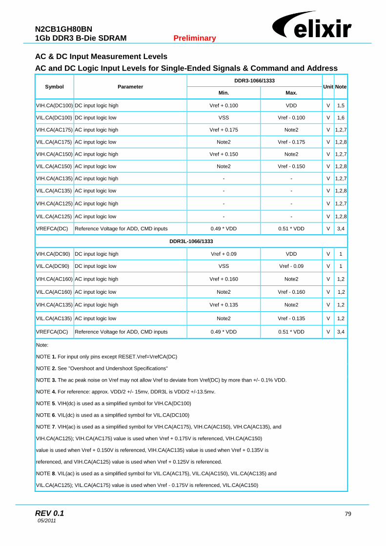
N2CB1GH80BN 1Gb DDR3 B-Die SDRAM Preliminary
REV 0.1 79 05/2011
AC & DC Input Measurement Levels
AC and DC Logic Input Levels for Single-Ended Signals & Command and Address
Symbol Parameter DDR3-1066/1333
Unit Note Min. Max.
VIH.CA(DC100) DC input logic high Vref + 0.100 VDD V 1,5
VIL.CA(DC100) DC input logic low VSS Vref - 0.100 V 1,6
VIH.CA(AC175) AC input logic high Vref + 0.175 Note2 V 1,2,7
VIL.CA(AC175) AC input logic low Note2 Vref - 0.175 V 1,2,8
VIH.CA(AC150) AC input logic high Vref + 0.150 Note2 V 1,2,7
VIL.CA(AC150) AC input logic low Note2 Vref - 0.150 V 1,2,8
VIH.CA(AC135) AC input logic high - - V 1,2,7
VIL.CA(AC135) AC input logic low - - V 1,2,8
VIH.CA(AC125) AC input logic high - - V 1,2,7
VIL.CA(AC125) AC input logic low - - V 1,2,8
VREFCA(DC) Reference Voltage for ADD, CMD inputs 0.49 * VDD 0.51 * VDD V 3,4
DDR3L-1066/1333
VIH.CA(DC90) DC input logic high Vref + 0.09 VDD V 1
VIL.CA(DC90) DC input logic low VSS Vref - 0.09 V 1
VIH.CA(AC160) AC input logic high Vref + 0.160 Note2 V 1,2
VIL.CA(AC160) AC input logic low Note2 Vref - 0.160 V 1,2
VIH.CA(AC135) AC input logic high Vref + 0.135 Note2 V 1,2
VIL.CA(AC135) AC input logic low Note2 Vref - 0.135 V 1,2
VREFCA(DC) Reference Voltage for ADD, CMD inputs 0.49 * VDD 0.51 * VDD V 3,4
Note:
NOTE 1. For input only pins except RESET.Vref=VrefCA(DC)
NOTE 2. See "Overshoot and Undershoot Specifications"
NOTE 3. The ac peak noise on Vref may not allow Vref to deviate from Vref(DC) by more than +/- 0.1% VDD.
NOTE 4. For reference: approx. VDD/2 +/- 15mv, DDR3L is VDD/2 +/-13.5mv.
NOTE 5. VIH(dc) is used as a simplified symbol for VIH.CA(DC100)
NOTE 6. VIL(dc) is used as a simplified symbol for VIL.CA(DC100)
NOTE 7. VIH(ac) is used as a simplified symbol for VIH.CA(AC175), VIH.CA(AC150), VIH.CA(AC135), and
VIH.CA(AC125); VIH.CA(AC175) value is used when Vref + 0.175V is referenced, VIH.CA(AC150)
value is used when Vref + 0.150V is referenced, VIH.CA(AC135) value is used when Vref + 0.135V is
referenced, and VIH.CA(AC125) value is used when Vref + 0.125V is referenced.
NOTE 8. VIL(ac) is used as a simplified symbol for VIL.CA(AC175), VIL.CA(AC150), VIL.CA(AC135) and
VIL.CA(AC125); VIL.CA(AC175) value is used when Vref - 0.175V is referenced, VIL.CA(AC150)

N2CB1GH80BN 1Gb DDR3 B-Die SDRAM Preliminary
REV 0.1 80 05/2011
value is used when Vref - 0.150V is referenced, VIL.CA(AC135) value is used when Vref - 0.135V is
referenced, and VIL.CA(AC125) value is used when Vref - 0.125V is referenced.
AC and DC Logic Input Levels for Single-Ended Signals & DQ and DM
Symbol Parameter
DDR3-1066 DDR3-1333
Unit Note
Min. Max. Min. Max.
VIH.DQ(DC100) DC input logic high Vref + 0.100 VDD Vref +
0.100 VDD V 1,5
VIL.DQ(DC100) DC input logic low VSS Vref - 0.100 VSS Vref –
0.100 V 1,6
VIH.DQ(AC175) AC input logic high Vref + 0.175 Note2 Vref + 0.150 Note2 V 1,2,7,9
VIL.DQ(AC175) AC input logic low Note2 Vref - 0.175 Note2 Vref –
0.150 V 1,2,8,9
VIH.DQ(AC150) AC input logic high Vref + 0.150 Note2 Vref +
0.150 Note2 V 1,2,7,9
VIL.DQ(AC150) AC input logic low Note2 Vref - 0.150 Note2 Vref –
0.150 V 1,2,8,9
VIH.DQ(AC135) AC input logic high - - - - mV 1,2,7
VIL.DQ(AC135) AC input logic low - - - - mV 1,2,8
VREFDQ(DC) Reference Voltage for
DQ, DM inputs 0.49 * VDD 0.51 * VDD
0.49 *
VDD
0.51 *
VDD V 3,4
Note:
NOTE 1. For input only pins except RESET.Vref=VrefCA(DC)
NOTE 2. See "Overshoot and Undershoot Specifications"
NOTE 3. The ac peak noise on Vref may not allow Vref to deviate from Vref(DC) by more than +/- 0.1% VDD.
NOTE 4. For reference: approx. VDD/2 +/- 15mv, DDR3L is VDD/2 +/-13.5mv.
NOTE 5. VIH(dc) is used as a simplified symbol for VIH.CA(DC100)
NOTE 6. VIL(dc) is used as a simplified symbol for VIL.CA(DC100)
NOTE 7. VIH(ac) is used as a simplified symbol for VIH.CA(AC175), VIH.CA(AC150), VIH.CA(AC135), and
VIH.CA(AC125); VIH.CA(AC175) value is used when Vref + 0.175V is referenced, VIH.CA(AC150)
value is used when Vref + 0.150V is referenced, VIH.CA(AC135) value is used when Vref + 0.135V is
referenced, and VIH.CA(AC125) value is used when Vref + 0.125V is referenced.
NOTE 8. VIL(ac) is used as a simplified symbol for VIL.CA(AC175), VIL.CA(AC150), VIL.CA(AC135) and
VIL.CA(AC125); VIL.CA(AC175) value is used when Vref - 0.175V is referenced, VIL.CA(AC150)
value is used when Vref - 0.150V is referenced, VIL.CA(AC135) value is used when Vref - 0.135V is
referenced, and VIL.CA(AC125) value is used when Vref - 0.125V is referenced.
NOTE 9. These levels apply for 1.35 Volt operation only. If the device is operated at 1.5V, the respective levels in
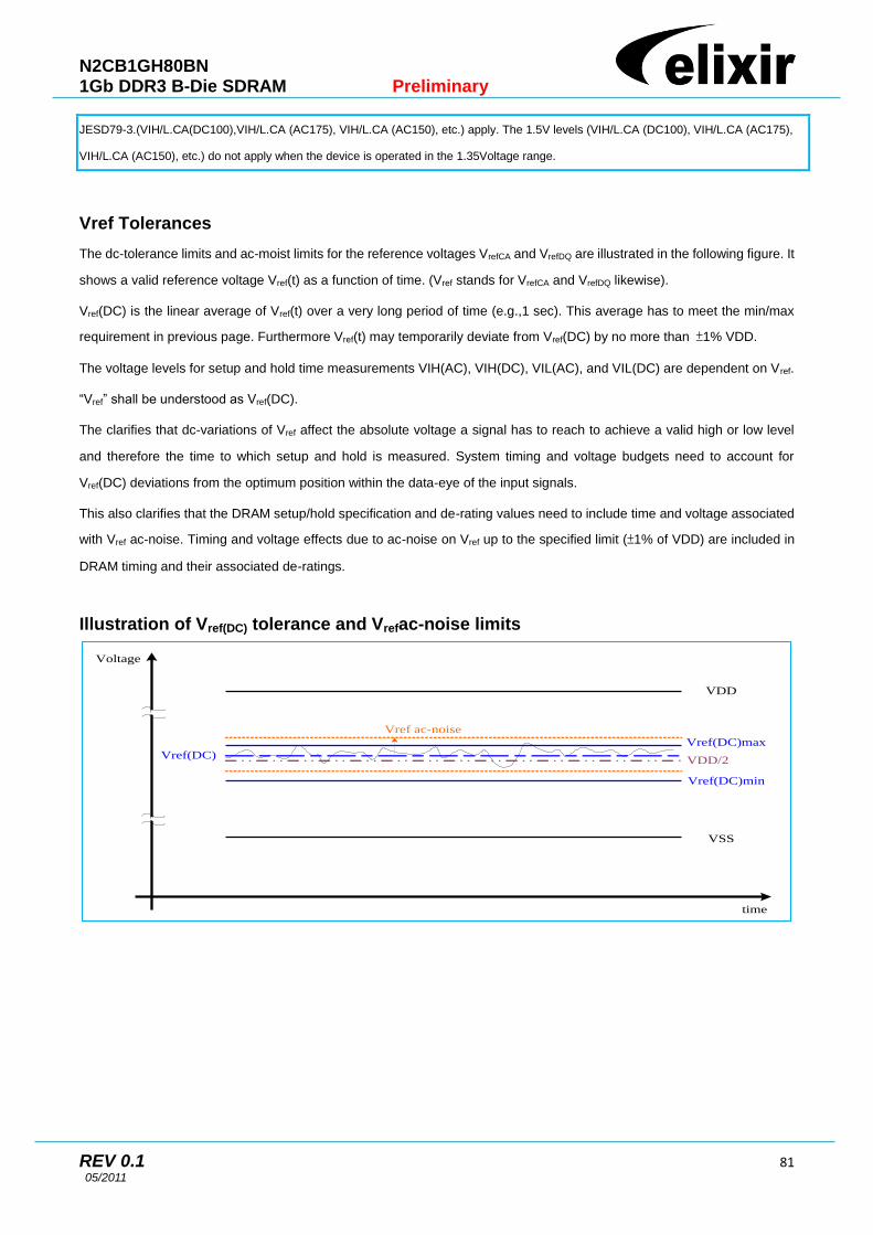
N2CB1GH80BN 1Gb DDR3 B-Die SDRAM Preliminary
REV 0.1 81 05/2011
JESD79-3.(VIH/L.CA(DC100),VIH/L.CA (AC175), VIH/L.CA (AC150), etc.) apply. The 1.5V levels (VIH/L.CA (DC100), VIH/L.CA (AC175),
VIH/L.CA (AC150), etc.) do not apply when the device is operated in the 1.35Voltage range.
Vref Tolerances
The dc-tolerance limits and ac-moist limits for the reference voltages VrefCA and VrefDQ are illustrated in the following figure. It
shows a valid reference voltage Vref(t) as a function of time. (Vref stands for VrefCA and VrefDQ likewise).
Vref(DC) is the linear average of Vref(t) over a very long period of time (e.g.,1 sec). This average has to meet the min/max
requirement in previous page. Furthermore Vref(t) may temporarily deviate from Vref(DC) by no more than ±1% VDD.
The voltage levels for setup and hold time measurements VIH(AC), VIH(DC), VIL(AC), and VIL(DC) are dependent on Vref.
“Vref” shall be understood as Vref(DC).
The clarifies that dc-variations of Vref affect the absolute voltage a signal has to reach to achieve a valid high or low level
and therefore the time to which setup and hold is measured. System timing and voltage budgets need to account for
Vref(DC) deviations from the optimum position within the data-eye of the input signals.
This also clarifies that the DRAM setup/hold specification and de-rating values need to include time and voltage associated
with Vref ac-noise. Timing and voltage effects due to ac-noise on Vref up to the specified limit (±1% of VDD) are included in
DRAM timing and their associated de-ratings.
Illustration of Vref(DC) tolerance and Vrefac-noise limits
Vref(DC)
Vref(DC)max
Vref(DC)min
VDD/2
Vref ac-noise
Voltage
time
VDD
VSS

N2CB1GH80BN 1Gb DDR3 B-Die SDRAM Preliminary
REV 0.1 82 05/2011
AC and DC Logic Input Levels for Differential Signals
Symbol Parameter DDR3-1066, 1333
Unit Notes Min. Max.
VIHdiff Differential input logic high +0.200 Note3 V 1
VILdiff Differential input logic low Note3 -0.200 V 1
VIHdiff(ac) Differential input high ac 2 x ( VIH(ac) – Vref ) Note3 V 2
VILdiff(ac) Differential input low ac Note3 2 x ( Vref - VIL(ac) ) V 2
Note:
1. Used to define a differential signal slew-rate.
2. For CK - CK use VIH/VIL(ac) of ADD/CMD and VREFCA; for DQS - DQS, DQSL, DQSL, DQSU, DQSU use VIH/VIL(ac)
of DQs and VREFDQ; if a reduced ac-high or ac-low level is used for a signal group, then the reduced level applies also
there.
3. These values are not defined, however the single-ended signals CK, CK, DQS, DQS, DQSL, DQSL, DQSU, DQSU need
to be within the respective limits (VIH(dc)max, VIL(dc)min) for single-ended signals as well as limitations for overshoot
and undershoot.
Definition of differential ac-swing and “time above ac-level”
Time
Diff
ere
ntialI
nputV
oltage
(i.e
.D
QS
–D
QS
,C
K–
CK
)
tDVAC
tDVAC
Half cycle
VIH.Diff.AC.min
VIH.Diff. DC min
VIL.Diff.AC.max
0
VIL. Diff. DC max

N2CB1GH80BN 1Gb DDR3 B-Die SDRAM Preliminary
REV 0.1 83 05/2011
Allowed time before ringback (tDVAC) for CK - and DQS -
Slew Rate [V/ns]
tDVAC [ps]
@IVIH/Ldiff(ac)I = 350mV
tDVAC [ps]
@IVIH/Ldiff(ac)I = 300mV
min max min max
> 4.0 75 - 175 -
4.0 57 - 170 -
3.0 50 - 167 -
2.0 38 - 163 -
1.8 34 - 162 -
1.6 29 - 161 -
1.4 22 - 159 -
1.2 13 - 155 -
1.0 0 - 150 -
< 1.0 0 - 150 -
1.35V
Slew Rate [V/ns]
tDVAC [ps]
@IVIH/Ldiff(ac)I = 320mV
tDVAC [ps]
@IVIH/Ldiff(ac)I = 270mV
Min. Max. Min. Max.
> 4.0 TBD - TBD -
4.0 TBD - TBD -
3.0 TBD - TBD -
2.0 TBD - TBD -
1.8 TBD - TBD -
1.6 TBD - TBD -
1.4 TBD - TBD -
1.2 TBD - TBD -
1.0 TBD - TBD -
< 1.0 TBD - TBD -

N2CB1GH80BN 1Gb DDR3 B-Die SDRAM Preliminary
REV 0.1 84 05/2011
Single-ended requirements for differential signals
Each individual component of a differential signal (CK, DQS, DQSL, DQSU,, ,, or ) has also to comply
with certain requirements for single-ended signals.
CK and have to approximately reach VSEHmin / VSELmax (approximately equal to the ac-levels (VIH(ac) / VIL(ac)) for
ADD/CMD signals) in every half-cycle. DQS, DQSL, DQSU, , have to reach VSEHmin / VSELmax (approxi-
mately the ac-levels (VIH(ac) / VIL(ac)) for DQ signals) in every half-cycle proceeding and following a valid transition.
Note that the applicable ac-levels for ADD/CMD and DQ‟s might be different per speed-bin etc. E.g., if
VIH150(ac)/VIL150(ac) is used for ADD/CMD signals, then these ac-levels apply also for the singleended
signals CK and
Single-ended levels for CK, DQS, DQSL, DQSU, , , , or
Symbol Parameter DDR3-1066, 1333
Unit Notes Min Max
VSEH Single-ended high-level for strobes (VDDQ/2) + 0.175 note3 V 1, 2
Single-ended high-level for CK, (VDDQ/2) + 0.175 note3 V 1, 2
VSEL Single-ended low-level for strobes note3 (VDDQ/2) - 0.175 V 1, 2
Single-ended Low-level for CK, note3 (VDDQ/2) - 0.175 V 1, 2
Note:
1. For CK, use VIH/VIL(ac) of ADD/CMD; for strobes (DQS, DQSL, DQSU, CK, , , or ) use VIH/VIL(ac)
of DQs.
2. VIH(ac)/VIL(ac) for DQs is based on VREFDQ; VIH(ac)/VIL(ac) for ADD/CMD is based on VREFCA; if a reduced ac-high
or ac-low level is used for a signal group, then the reduced level applies also there.
3. These values are not defined, however the single-ended signals CK, , DQS, , DQSL, , DQSU, need
to be within the respective limits (VIH(dc)max, VIL(dc)min) for single-ended signals as well as limitations for overshoot and
undershoot.
Differential Input Cross Point Voltage
To guarantee tight setup and hold times as well as output skew parameters with respect to clock and strobe, each cross
point voltage of differential input signals (CK, CK and DQS, DQS) must meet the requirements in the following table. The
differential input cross point voltage Vix is measured from the actual cross point of true and complete signal to the midlevel
between of VDD and VSS.

N2CB1GH80BN 1Gb DDR3 B-Die SDRAM Preliminary
REV 0.1 85 05/2011
Vix Definition
VDD
VSS
VDD/2
,
CK,DQS
VIX
VIX
VIX
Cross point voltage for differential input signals (CK, DQS)
Symbol Parameter DDR3-1066/1333
Unit Note Min. Max.
Vix
Differential Input Cross Point Voltage relative to VDD/2 for CK,
CK#
-150 150 mV
-175 175 mV 1
Differential Input Cross Point Voltage relative to VDD/2 for DQS,
DQS# -150 150 mV
Note 1: Extended range for Vix is only allowed for clock and if single-ended clock input signals CK and are monotonic
with a single-ended swing VSEL / VSEH of at least VDD/2 ± 250mV, and when the differential slew rate of CK - is
larger than 3V/ns.
Slew Rate Definition for Differential Input Signals
Input slew rate for differential signals (CK, CK# and DQS, DQS#) are defined and measured as shown below.

N2CB1GH80BN 1Gb DDR3 B-Die SDRAM Preliminary
REV 0.1 86 05/2011
Differential Input Slew Rate Definition
Description Measured
Defined by From To
Differential input slew rate for rising edge (CK-&
DQS-) VILdiffmax VIHdiffmin [VIHdiffmin-VILdiffmax] / DeltaTRdiff
Differential input slew rate for falling edge (CK- &
DQS-) VIHdiffmin VILdiffmax [VIHdiffmin-VILdiffmax] / DeltaTFdiff
The differential signal (i.e., CK-& DQS-) must be linear between these thresholds.
Input Nominal Slew Rate Definition for single ended signals
Delta
TFdiff
Delta
TRdiff
VIHdiffMin
VILdiffMax
0
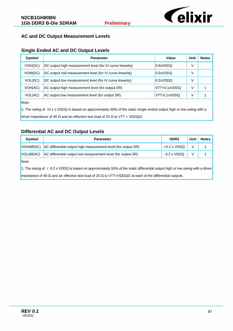
N2CB1GH80BN 1Gb DDR3 B-Die SDRAM Preliminary
REV 0.1 87 05/2011
AC and DC Output Measurement Levels
Single Ended AC and DC Output Levels
Symbol Parameter Value Unit Notes
VOH(DC) DC output high measurement level (for IV curve linearity) 0.8xVDDQ V
VOM(DC) DC output mid measurement level (for IV curve linearity) 0.5xVDDQ V
VOL(DC) DC output low measurement level (fro IV curve linearity) 0.2xVDDQ V
VOH(AC) AC output high measurement level (for output SR) VTT+0.1xVDDQ V 1
VOL(AC) AC output low measurement level (for output SR) VTT-0.1xVDDQ V 1
Note:
1. The swing of ±0.1 x VDDQ is based on approximately 50% of the static single ended output high or low swing with a
driver impedance of 40 Ω and an effective test load of 25 Ω to VTT = VDDQ/2.
Differential AC and DC Output Levels
Symbol Parameter DDR3 Unit Notes
VOHdiff(AC) AC differential output high measurement level (for output SR) +0.2 x VDDQ V 1
VOLdiff(AC) AC differential output low measurement level (for output SR) -0.2 x VDDQ V 1
Note:
1. The swing of ± 0.2 x VDDQ is based on approximately 50% of the static differential output high or low swing with a driver
impedance of 40 Ω and an effective test load of 25 Ω to VTT=VDDQ/2 at each of the differential outputs.

N2CB1GH80BN 1Gb DDR3 B-Die SDRAM Preliminary
REV 0.1 88 05/2011
Delta TFse
Delta TFse
VOH (AC)
VOL (AC)
VTT
Sing
le E
nded
Out
put V
olta
ge (
i.e. D
Q)
Single Ended Output Slew Rate
Description Measured
Defined by From To
Single ended output slew rate for rising edge VOL(AC) VOH(AC) [VOH(AC)-VOL(AC)] / DeltaTRse
Single ended output slew rate for falling edge VOH(AC) VOL(AC) [VOH(AC)-VOL(AC)] / DeltaTFse
Note: Output slew rate is verified by design and characterization, and may not be subject to production test.
Single Ended Output Slew Rate Definition

N2CB1GH80BN 1Gb DDR3 B-Die SDRAM Preliminary
REV 0.1 89 05/2011
Table 1: Differential Output Slew Rate
Description Measured
Defined by From To
Differential output slew rate for rising edge VOLdiff(AC) VOHdiff(AC) [VOHdiff(AC)-VOLdiff(AC)] / DeltaTRdiff
Differential output slew rate for falling edge VOHdiff(AC) VOLdiff(AC) [VOHdiff(AC)-VOLdiff(AC)] / DeltaTFdiff
Note: Output slew rate is verified by design and characterization, and may not be subject to production test.
Differential Output Slew Rate Definition
Differential Output Slew Rate
Parameter Symbol Operation
Voltag
DDR3-1066 DDR3-1333 Unit
Min. Max. Min. Max.
Single-ended Output Slew Rate SRQse
1.35V 3.5 12 3.5 12
V/ns 1.5V 5 10 5 10
Note:
SR: Slew Rate.
Q: Query Output (like in DQ, which stands for Data-in, Query -Output).
diff: Differential signals.
For Ron = RZQ/7 setting.
Delta TFse
Delta TFse
VOh diff (AC)
VOL diff (AC)
0
Diff
eren
tial O
utpu
t Vol
tage
(i.e
. DQ
S-D
QS
)
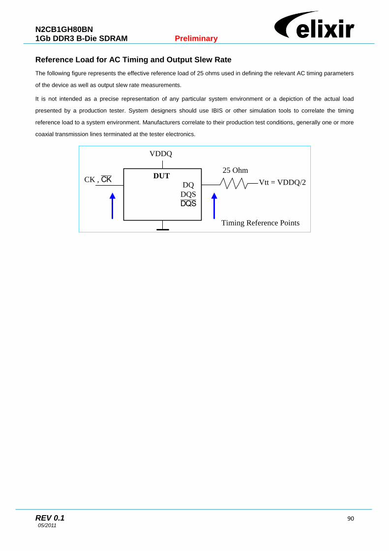
N2CB1GH80BN 1Gb DDR3 B-Die SDRAM Preliminary
REV 0.1 90 05/2011
Reference Load for AC Timing and Output Slew Rate
The following figure represents the effective reference load of 25 ohms used in defining the relevant AC timing parameters
of the device as well as output slew rate measurements.
It is not intended as a precise representation of any particular system environment or a depiction of the actual load
presented by a production tester. System designers should use IBIS or other simulation tools to correlate the timing
reference load to a system environment. Manufacturers correlate to their production test conditions, generally one or more
coaxial transmission lines terminated at the tester electronics.
Vtt = VDDQ/2
25 Ohm
CK ,
VDDQ
DUT
DQ
DQS
Timing Reference Points
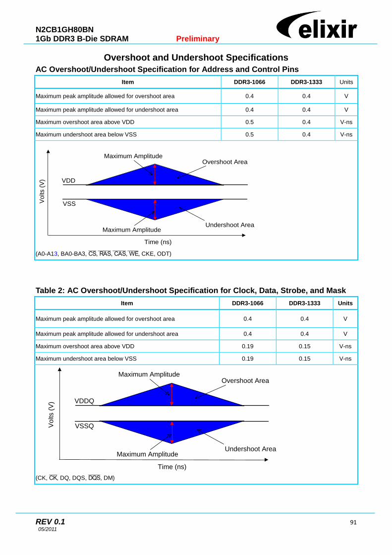
N2CB1GH80BN 1Gb DDR3 B-Die SDRAM Preliminary
REV 0.1 91 05/2011
Overshoot and Undershoot Specifications
AC Overshoot/Undershoot Specification for Address and Control Pins
Item DDR3-1066 DDR3-1333 Units
Maximum peak amplitude allowed for overshoot area 0.4 0.4 V
Maximum peak amplitude allowed for undershoot area 0.4 0.4 V
Maximum overshoot area above VDD 0.5 0.4 V-ns
Maximum undershoot area below VSS 0.5 0.4 V-ns
(A0-A13, BA0-BA3, ,,,, CKE, ODT)
Table 2: AC Overshoot/Undershoot Specification for Clock, Data, Strobe, and Mask
Item DDR3-1066 DDR3-1333 Units
Maximum peak amplitude allowed for overshoot area 0.4 0.4 V
Maximum peak amplitude allowed for undershoot area 0.4 0.4 V
Maximum overshoot area above VDD 0.19 0.15 V-ns
Maximum undershoot area below VSS 0.19 0.15 V-ns
(CK, , DQ, DQS, , DM)
VDD
VSS
Overshoot Area
Undershoot Area
Maximum Amplitude
Maximum Amplitude
Time (ns)
Vo
lts (
V)
VDDQ
VSSQ
Overshoot Area
Undershoot Area
Maximum Amplitude
Maximum Amplitude
Time (ns)
Vo
lts (
V)

N2CB1GH80BN 1Gb DDR3 B-Die SDRAM Preliminary
REV 0.1 92 05/2011
34 Ohm Output Driver DC Electrical Characteristics
A Functional representation of the output buffer is shown as below. Output driver impedance RON is defined by the value of
the external reference resistor RZQ as follows:
RON34 = RZQ / 7 (nominal 34.4ohms +/-10% with nominal RZQ=240ohms)
The individual pull-up and pull-down resistors (RONPu and RONPd) are defined as follows:
RONPu = [VDDQ-Vout] / l Iout l ------------------- under the condition that RONPd is turned off (1)
RONPd = Vout / I Iout I -------------------------------under the condition that RONPu is turned off (2)
Output Driver: Definition of Voltages and Currents
To
othercircuitry
like
RCV, ...
RON
RON
Pu
Pd
I Pu
I Pd
VDDQ
VSSQ
DQI Out
V Out
Output Driver
Chip in Drive Mode
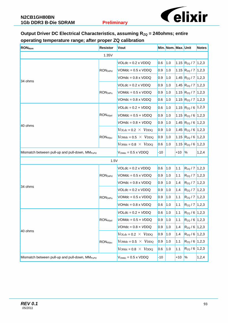
N2CB1GH80BN 1Gb DDR3 B-Die SDRAM Preliminary
REV 0.1 93 05/2011
Output Driver DC Electrical Characteristics, assuming RZQ = 240ohms; entire
operating temperature range; after proper ZQ calibration
RONNom Resistor Vout Min. Nom. Max. Unit Notes
1.35V
34 ohms
RON34Pd
VOLdc = 0.2 x VDDQ 0.6 1.0 1.15 RZQ / 7 1,2,3
VOMdc = 0.5 x VDDQ 0.9 1.0 1.15 RZQ / 7 1,2,3
VOHdc = 0.8 x VDDQ 0.9 1.0 1.45 RZQ / 7 1,2,3
RON34Pu
VOLdc = 0.2 x VDDQ 0.9 1.0 1.45 RZQ / 7 1,2,3
VOMdc = 0.5 x VDDQ 0.9 1.0 1.15 RZQ / 7 1,2,3
VOHdc = 0.8 x VDDQ 0.6 1.0 1.15 RZQ / 7 1,2,3
40 ohms
RON40pd
VOLdc = 0.2 × VDDQ 0.6 1.0 1.15 RZQ / 6 1,2,3
VOMdc = 0.5 × VDDQ 0.9 1.0 1.15 RZQ / 6 1,2,3
VOHdc = 0.8 × VDDQ 0.9 1.0 1.45 RZQ / 6 1,2,3
RON40pu
VOLdc = 0.2 × VDDQ 0.9 1.0 1.45 RZQ / 6 1,2,3
VOMdc = 0.5 × VDDQ 0.9 1.0 1.15 RZQ / 6 1,2,3
VOHdc = 0.8 × VDDQ 0.6 1.0 1.15 RZQ / 6 1,2,3
Mismatch between pull-up and pull-down, MMPuPd VOMdc = 0.5 x VDDQ -10 +10 % 1,2,4
1.5V
34 ohms
RON34Pd
VOLdc = 0.2 x VDDQ 0.6 1.0 1.1 RZQ / 7 1,2,3
VOMdc = 0.5 x VDDQ 0.9 1.0 1.1 RZQ / 7 1,2,3
VOHdc = 0.8 x VDDQ 0.9 1.0 1.4 RZQ / 7 1,2,3
RON34Pu
VOLdc = 0.2 x VDDQ 0.9 1.0 1.4 RZQ / 7 1,2,3
VOMdc = 0.5 x VDDQ 0.9 1.0 1.1 RZQ / 7 1,2,3
VOHdc = 0.8 x VDDQ 0.6 1.0 1.1 RZQ / 7 1,2,3
40 ohms
RON40pd
VOLdc = 0.2 × VDDQ 0.6 1.0 1.1 RZQ / 6 1,2,3
VOMdc = 0.5 × VDDQ 0.9 1.0 1.1 RZQ / 6 1,2,3
VOHdc = 0.8 × VDDQ 0.9 1.0 1.4 RZQ / 6 1,2,3
RON40pu
VOLdc = 0.2 × VDDQ 0.9 1.0 1.4 RZQ / 6 1,2,3
VOMdc = 0.5 × VDDQ 0.9 1.0 1.1 RZQ / 6 1,2,3
VOHdc = 0.8 × VDDQ 0.6 1.0 1.1 RZQ / 6 1,2,3
Mismatch between pull-up and pull-down, MMPuPd VOMdc = 0.5 x VDDQ -10 +10 % 1,2,4
N2CB1GH80BN 1Gb DDR3 B-Die SDRAM Preliminary
REV 0.1 94 05/2011
Note:
1. The tolerance limits are specified after calibration with stable voltage and temperature. For the behavior of the tolerance
limits if temperature or voltage changes after calibration, see following section on voltage and temperature sensitivity.
2. The tolerance limits are specified under the condition that VDDQ = VDD and that VSSQ = VSS.
3. Pull-down and pull-up output driver impedances are recommended to be calibrated at 0.5 x VDDQ. Other calibration
schemes may be used to achieve the linearity spec shown above. e.g. calibration at 0.2 x VDDQ and 0.8 x VDDQ.
4. Measurement definition for mismatch between pull-up and pull-down, MMPuPd:
Measure RONPu and RONPd, but at 0.5 x VDDQ:
MMPuPd = [RONPu - RONPd] / RONNom x 100
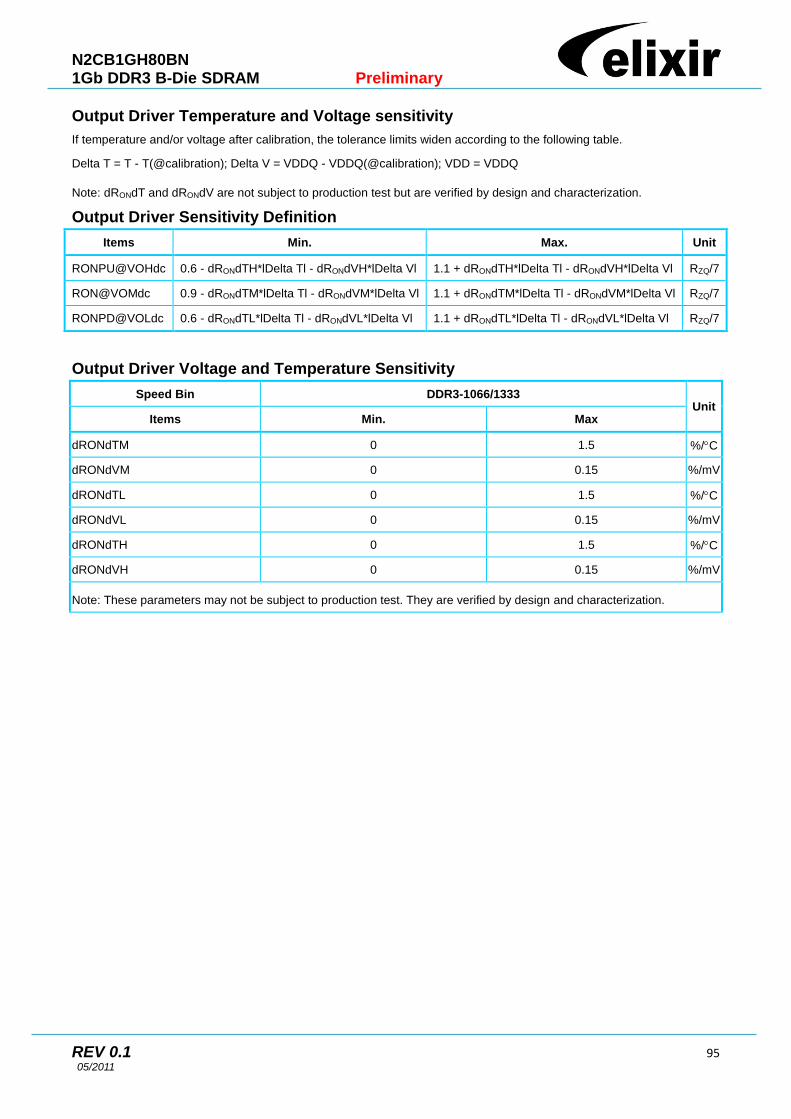
N2CB1GH80BN 1Gb DDR3 B-Die SDRAM Preliminary
REV 0.1 95 05/2011
Output Driver Temperature and Voltage sensitivity
If temperature and/or voltage after calibration, the tolerance limits widen according to the following table.
Delta T = T - T(@calibration); Delta V = VDDQ - VDDQ(@calibration); VDD = VDDQ
Note: dRONdT and dRONdV are not subject to production test but are verified by design and characterization.
Output Driver Sensitivity Definition
Items Min. Max. Unit
RONPU@VOHdc 0.6 - dRONdTH*lDelta Tl - dRONdVH*lDelta Vl 1.1 + dRONdTH*lDelta Tl - dRONdVH*lDelta Vl RZQ/7
RON@VOMdc 0.9 - dRONdTM*lDelta Tl - dRONdVM*lDelta Vl 1.1 + dRONdTM*lDelta Tl - dRONdVM*lDelta Vl RZQ/7
RONPD@VOLdc 0.6 - dRONdTL*lDelta Tl - dRONdVL*lDelta Vl 1.1 + dRONdTL*lDelta Tl - dRONdVL*lDelta Vl RZQ/7
Output Driver Voltage and Temperature Sensitivity
Speed Bin DDR3-1066/1333 Unit
Items Min. Max
dRONdTM 0 1.5 %/C
dRONdVM 0 0.15 %/mV
dRONdTL 0 1.5 %/C
dRONdVL 0 0.15 %/mV
dRONdTH 0 1.5 %/C
dRONdVH 0 0.15 %/mV
Note: These parameters may not be subject to production test. They are verified by design and characterization.

N2CB1GH80BN 1Gb DDR3 B-Die SDRAM Preliminary
REV 0.1 96 05/2011
On-Die Termination (ODT) Levels and I-V Characteristics
On-Die Termination effective resistance RTT is defined by bits A9, A6, and A2 of the MR1 Register.
ODT is applied to the DQ, DM, DQS/, and TDQS/ (x8 devices only) pins.
A functional representation of the on-die termination is shown in the following figure. The individual pull-up and pull-down
resistors (RTTPu and RTTPd) are defined as follows:
RTTPu = [VDDQ - Vout] / I Iout I ------------------ under the condition that RTTPd is turned off (3)
RTTPd = Vout / I Iout I ------------------------------ under the condition that RTTPu is turned off (4)
On-Die Termination: Definition of Voltages and Currents
ODT DC Electrical Characteristics
The following table provides an overview of the ODT DC electrical characteristics. The values for RTT60Pd120, RTT60Pu120,
RTT120Pd240, RTT120Pu240, RTT40Pd80, RTT40Pu80, RTT30Pd60, RTT30Pu60, RTT20Pd40, RTT20Pu40 are not specification
requirements, but can be used as design guide lines:
To other
circuitry
like
RCV, ...
RTT
RTT
Pu
Pd
I Pu
I Pd
VDDQ
VSSQ
DQI Out
V Out
ODT
Chip in Termination Mode
I = I - IOut Pd Pu

N2CB1GH80BN 1Gb DDR3 B-Die SDRAM Preliminary
REV 0.1 97 05/2011
ODT DC Electrical Characteristics, assuming RZQ = 240ohms +/- 1% entire operating
temperature range; after proper ZQ calibration
MR1 A9,A6,A2 RTT Resistor Vout Min. Nom. Max. Unit Notes
1.5V
0,1,0 120Ω
RTT120Pd240
VOLdc = 0.2 x VDDQ 0.6 1 1.1 RZQ 1,2,3,4
0.5 x VDDQ 0.9 1 1.1 RZQ 1,2,3,4
VOHdc = 0.8 x VDDQ 0.9 1 1.4 RZQ 1,2,3,4
RTT120Pu240
VOLdc = 0.2 x VDDQ 0.9 1 1.4 RZQ 1,2,3,4
0.5 x VDDQ 0.9 1 1,1 RZQ 1,2,3,4
VOHdc = 0.8 x VDDQ 0.6 1 1.1 RZQ 1,2,3,4
RTT120 VIL(ac) to VIH(ac) 0.9 1 1.6 RZQ /2 1,2,5
0, 0, 1 60Ω
RTT60Pd120
VOLdc = 0.2 x VDDQ 0.6 1 1.1 RZQ/2 1,2,3,4
0.5 x VDDQ 0.9 1 1.1 RZQ/2 1,2,3,4
VOHdc = 0.8 x VDDQ 0.9 1 1.4 RZQ/2 1,2,3,4
RTT60Pu120
VOLdc = 0.2 x VDDQ 0.9 1 1.4 RZQ/2 1,2,3,4
0.5 x VDDQ 0.9 1 1.1 RZQ/2 1,2,3,4
VOHdc = 0.8 x VDDQ 0.6 1 1.1 RZQ/2 1,2,3,4
RTT60 VIL(ac) to VIH(ac) 0.9 1 1.6 RZQ/4 1,2,5
0, 1, 1 40Ω
RTT40Pd80
VOLdc = 0.2 x VDDQ 0.6 1 1.1 RZQ/3 1,2,3,4
0.5 x VDDQ 0.9 1 1.1 RZQ/3 1,2,3,4
VOHdc = 0.8 x VDDQ 0.9 1 1.4 RZQ/3 1,2,3,4
RTT40Pu80
VOLdc = 0.2 x VDDQ 0.9 1 1.4 RZQ/3 1,2,3,4
0.5 x VDDQ 0.9 1 1.1 RZQ/3 1,2,3,4
VOHdc = 0.8 x VDDQ 0.6 1 1.1 RZQ/3 1,2,3,4
RTT40 VIL(ac) to VIH(ac) 0.9 1 1.6 RZQ/6 1,2,5
1, 0, 1 30Ω
RTT30Pd60
VOLdc = 0.2 x VDDQ 0.6 1 1.1 RZQ/4 1,2,3,4
0.5 x VDDQ 0.9 1 1.1 RZQ/4 1,2,3,4
VOHdc = 0.8 x VDDQ 0.9 1 1.4 RZQ/4 1,2,3,4
RTT30Pu60
VOLdc = 0.2 x VDDQ 0.9 1 1.4 RZQ/4 1,2,3,4
0.5 x VDDQ 0.9 1 1.1 RZQ/4 1,2,3,4
VOHdc = 0.8 x VDDQ 0.6 1 1.1 RZQ/4 1,2,3,4
RTT30 VIL(ac) to VIH(ac) 0.9 1 1.6 RZQ/8 1,2,5
1, 0, 0 20Ω
RTT20Pd40
VOLdc = 0.2 x VDDQ 0.6 1 1.1 RZQ/6 1,2,3,4
0.5 x VDDQ 0.9 1 1.1 RZQ/6 1,2,3,4
VOHdc = 0.8 x VDDQ 0.9 1 1.4 RZQ/6 1,2,3,4
RTT20Pu40
VOLdc = 0.2 x VDDQ 0.9 1 1.4 RZQ/6 1,2,3,4
0.5 x VDDQ 0.9 1 1.1 RZQ/6 1,2,3,4
VOHdc = 0.8 x VDDQ 0.6 1 1.1 RZQ/6 1,2,3,4
RTT20 VIL(ac) to VIH(ac) 0.9 1 1.6 RZQ/12 1,2,5
Deviation of VM w.r.t. VDDQ/2, DVM -5 +5 % 1,2,5,6

N2CB1GH80BN 1Gb DDR3 B-Die SDRAM Preliminary
REV 0.1 98 05/2011
Note: 1. The tolerance limits are specified after calibration with stable voltage and temperature. For the behavior of the tolerance
limits if temperature or voltage changes after calibration, see following section on voltage and temperature sensitivity. 2. The tolerance limits are specified under the condition that VDDQ = VDD and that VSSQ = VSS. 3. Pull-down and pull-up ODT resistors are recommended to be calibrated at 0.5 x VDDQ. Other calibration may be used to
achieve the linearity spec shown above. 4. Not a specification requirement, but a design guide line. 5. Measurement definition for RTT:
Apply VIH(ac) to pin under test and measure current / (VIH(ac)), then apply VIL(ac) to pin under test and measure current / (VIL(ac)) respectively. RTT = [VIH(ac) - VIL(ac)] / [I(VIH(ac)) - I(VIL(ac))]
6. Measurement definition for VM and DVM: Measure voltage (VM) at test pin (midpoint) with no lead: Delta VM = [2VM / VDDQ -1] x 100
ODT Temperature and Voltage sensitivity
If temperature and/or voltage after calibration, the tolerance limits widen according to the following table.
Delta T = T - T(@calibration); Delta V = VDDQ - VDDQ(@calibration); VDD = VDDQ
ODT Sensitivity Definition
Min. Max. Unit
RTT 0.9 - dRTTdT*lDelta Tl - dRTTdV*lDelta Vl 1.6 + dRTTdT*lDelta Tl + dRTTdV*lDelta Vl RZQ/2,4,6,8,12
ODT Voltage and Temperature Sensitivity
Min. Max. Unit
dRTTdT 0 1.5 %/C
dRTTdV 0 0.15 %/mV
Note: These parameters may not be subject to production test. They are verified by design and characterization.
Test Load for ODT Timings
Different than for timing measurements, the reference load for ODT timings is defined in the following figure.
ODT Timing Reference Load
Vtt =
25 Ohm
CK ,
VDDQ
DUT
Timing Reference Points
VSSQ
RTT=
DQ , DM
DQS ,
TDQS ,
VSSQ

N2CB1GH80BN 1Gb DDR3 B-Die SDRAM Preliminary
REV 0.1 99 05/2011
ODT Timing Definitions
Definitions for tAON, tAONPD, tAOF, tAOFPD, and tADC are provided in the following table and subsequent figures.
Symbol Begin Point Definition End Point Definition
tAON Rising edge of CK - CK defined by the end point of ODTLon Extrapolated point at VSSQ
tAONPD Rising edge of CK - CK with ODT being first registered high Extrapolated point at VSSQ
tAOF Rising edge of CK - CK defined by the end point of ODTLoff End point: Extrapolated point at VRTT_Nom
tAOFPD Rising edge of CK - CK with ODT being first registered low End point: Extrapolated point at VRTT_Nom
tADC Rising edge of CK - CK defined by the end point of ODTLcnw,
ODTLcwn4, or ODTLcwn8
End point: Extrapolated point at VRTT_Wr and
VRTT_Nom respectively
Reference Settings for ODT Timing Measurements
Measured Parameter RTT_Nom Setting RTT_Wr Setting VSW1[V] VSW2[V] Note
tAON RZQ/4 NA 0.05 0.10
RZQ/12 NA 0.10 0.20
tAONPD RZQ/4 NA 0.05 0.10
RZQ/12 NA 0.10 0.20
tAOF RZQ/4 NA 0.05 0.10
RZQ/12 NA 0.10 0.20
tAOFPD RZQ/4 NA 0.05 0.10
RZQ/12 NA 0.10 0.20
tADC RZQ/12 RZQ/2 0.20 0.30
Definition of tAON
tAON
Tsw2
Tsw1
Vsw1
Vsw2
VSSQ
VTT
DQ, DM
DQS, DQS#
TDQS, TDQS#
End point: Extrapolated point at VSSQ
CK
CK#
Begin point: Rising edge of CK – CK#
Defined by the end point of ODTLon

N2CB1GH80BN 1Gb DDR3 B-Die SDRAM Preliminary
REV 0.1 100 05/2011
Definition of tAONPD
Definition of tAOF
Definition of tAOFPD
tAONPD
Tsw2
Tsw1
Vsw1
Vsw2
VSSQ
VTT
DQ, DM
DQS, DQS#
TDQS, TDQS#
End point: Extrapolated point at VSSQ
CK
CK#
Begin point: Rising edge of CK – CK#
with ODT being first register high
tAOF
Tsw2
Tsw1
Vsw1
Vsw2
VSSQ
VTT
DQ, DM
DQS, DQS#
TDQS, TDQS#
End point: Extrapolated point at VRTT_Nom
CK
CK#
Begin point: Rising edge of CK – CK#
defined by the end point of ODTLoff
VRTT_Nom
tAOFPD
Tsw2
Tsw1
Vsw1
Vsw2
VSSQ
VTT
DQ, DM
DQS, DQS#
TDQS, TDQS#
End point: Extrapolated point at VRTT_Nom
CK
CK#
Begin point: Rising edge of CK – CK#
with ODT being first registered low
VRTT_Nom

N2CB1GH80BN 1Gb DDR3 B-Die SDRAM Preliminary
REV 0.1 101 05/2011
Definition of tADC
tADC
Tsw21
Tsw11
Vsw1Vsw2
DQ, DM
DQS, DQS#
TDQS, TDQS#
End point: Extrapolated point at VRTT_Nom
CK
CK#
Begin point: Rising edge of CK – CK#
defined by the end of ODTLcnw
VRTT_Nom
tADC
Tsw22
Tsw12
VSSQ
VTT
End point: Extrapolated point at VRTT_Wr
CK
CK#
Begin point: Rising edge of CK – CK# defined
by the end of ODTLcwn4 or ODTLcwn8
VRTT_Wr
VRTT_Nom

N2CB1GH80BN 1Gb DDR3 B-Die SDRAM Preliminary
REV 0.1 102 05/2011
Input / Output Capacitance
Symbol Parameter
DDR3-1066 DDR3-1333
Units Notes
Min. Max Min. Max
CIO Input/output capacitance (DQ, DM, DQS,, TDQS,
) 1.50 3.00 1.50 2.50 pF 1,2,3
CCK Input capacitance, CK and CK 0.80 1.60 0.80 1.40 pF 2,3
CDCK Input capacitance delta, CK and 0.00 0.15 0.00 0.15 pF 2,3,4
CDDQS Input/output capacitance delta, DQS and 0.00 0.20 0.00 0.15 pF 2,3,5
CI Input capacitance, CTRL, ADD, CMD input-only pins 0.75 1.35 0.75 1.30 pF 2,3,7,8
CDI_CTRL Input capacitance delta, all CTRL input-only pins -0.50 0.30 -0.40 0.20 pF 2,3,7,8
CDI_ADD_CMD Input capacitance delta, all ADD/CMD input-only pins -0.50 0.50 -0.40 0.40 pF 2,3,9,10
CDIO Input/output capacitance delta, DQ, DM, DQS, ,
TDQS, -0.50 0.30 -0.50 0.30 pF 2,3,11
CZQ Input/output capacitance of ZQ pin - 3.00 - 3.00 pF 2,3,12
1. Although the DM, TDQS and TDQS pins have different functions, the loading matches DQ and DQS
2. This parameter is not subject to production test. It is verified by design and characterization. VDD=VDDQ=1.5V, VBIAS=VDD/2 and
on-die termination off.
3. This parameter applies to monolithic devices only; stacked/dual-die devices are not covered here
4. Absolute value of CCK-CCK
5. Absolute value of CIO(DQS)-CIO(DQS)
6. CI applies to ODT, , CKE, A0-A13, BA0-BA2, , ,.
7. CDI_CTRL applies to ODT, and CKE
8. CDI_CTRL=CI(CTRL)-0.5*(CI(CLK)+CI(CLK))
9. CDI_ADD_CMD applies to A0-A13, BA0-BA2, , and
10. CDI_ADD_CMD=CI(ADD_CMD) - 0.5*(CI(CLK)+CI())
11. CDIO=CIO(DQ,DM) - 0.5*(CIO(DQS)+CIO))
12. Maximum external load capacitance on ZQ pin: 5 pF.

N2CB1GH80BN 1Gb DDR3 B-Die SDRAM Preliminary
REV 0.1 103 05/2011
IDD Specifications and Measurement Conditions
Table 3: IDD Specifications (x16)
Symbol Parameter/Condition Operation
Voltage
DDR3-1066 DDR3-1333 Unit
Typ. Max. Typ. Max.
IDD0 Operating Current 0 -> One Bank Activate-> Precharge
1.5V 63 76 66 80
mA 1.35V TBD TBD TBD TBD
IDD1 Operating Current 1 -> One Bank Activate-> Read-> Precharge
1.5V 87 106 92 112
mA 1.35V TBD TBD TBD TBD
IDD2P0 Precharge Power-Down Current Slow Exit - MR0 bit A12 = 0
1.5V 5 12 5 13
mA 1.35V TBD TBD TBD TBD
IDD2P1 Precharge Power-Down Current Fast Exit - MR0 bit A12 = 1
1.5V 16 21 18 23
mA 1.35V TBD TBD TBD TBD
IDD2Q Precharge Quiet Standby Current 1.5V 26 31 29 34
mA 1.35V TBD TBD TBD TBD
IDD2N Precharge Standby Current 1.5V 27 33 30 35
mA 1.35V TBD TBD TBD TBD
IDD3P Active Power-Down Current Always Fast Exit
1.5V 17 25 20 27
mA 1.35V TBD TBD TBD TBD
IDD3N Active Standby Current
1.5V 29 38 33 41
mA 1.35V TBD TBD TBD TBD
IDD4R Operating Current Burst Read
1.5V 132 165 157 195
mA 1.35V TBD TBD TBD TBD
IDD4W Operating Current Burst Write 1.5V 130 162 152 189
mA 1.35V TBD TBD TBD TBD
IDD5B Burst Refresh Current
1.5V 124 136 133 149
mA 1.35V TBD TBD TBD TBD
IDD6 Self-Refresh Current Normal Temperature Range (0-85°C)
1.5V 4 7 4 7
mA 1.35V TBD TBD TBD TBD
IDD6ET Self-Refresh Current: extended temperature range
1.5V 4 8 4 8
mA 1.35V TBD TBD TBD TBD
IDD6TC Auto Self-Refresh Current 1.5V 4 8 4 8
mA 1.35V TBD TBD TBD TBD
IDD7 All Bank Interleave Read Current
1.5V 212 266 236 297
mA 1.35V TBD TBD TBD TBD

N2CB1GH80BN 1Gb DDR3 B-Die SDRAM Preliminary
REV 0.1 104 05/2011
Table 4: IDD Measurement Conditions
Symbol Parameter/Condition
IDD0
Operating Current - One bank Active - Precharge current CKE: High; External clock: On; tCK, tRC, tRAS: see table in the next page; CS: High between ACT and PRE; Command Inputs: SWITCHING
1 (except for ACT and PRE); Row, Column Address, Data I/O: SWITCHING1
(A10 Low permanently); Bank Address: fixed (Bank 0); Output Buffer: off 2
; ODT: disabled 3; Active Banks: one
(ACT-PRE loop); Idle Banks: all other; Pattern example: A0 D DD DD DD DD DD DD D P0.4
IDD1
Operating One bank Active-Read-Precharge Current CKE: High; External clock: On; tCK, tRC, tRAS, tRCD, CL, AL: see table in the next page; CS: High between ACT, RD, and PRE; Command Inputs: SWITCHING
1 (except ACT, RD, and PRE Commands); Row, Column
Address: SWITCHING1 (A10 Low permanently); Bank Address: fixed (Bank 0); Data I/O: switching every clock (RD Data stable during one Clock cycle); floating when no burst activity; Output Buffer: Off
2; ODT: disabled
3;
Burst Length: BL85; Active Banks: one (ACT-RD-PRE loop); Idle Banks: all other; Pattern example: A0 D DD D R0 DD DD DD DD D P0
4.
IDD2N Precharge Standby Current CKE=High; External Clock=On; tCK: see table in the next page; CS: High; Command Inputs, Row, Column, Bank Address, Data I/O: SWITCHING
1; Output Buffer: Off
2; ODT: disabled
3; Active / Idle Banks: none / all.
IDD2P(0)
Precharge Power-Down Current - (Slow Exit) CKE=Low; External Clock=On; tCK: see table in the next page; CS: Stable; Command Inputs: Stable; Row, Column / Bank Address: Stable; Data I/O: floating; Output Buffer: Off
2; ODT: disabled
3; Active / Idle Banks:
none / all. Precharge Power Down Mode: Slow Exit 6(RD and ODT must satisfy tXPDLL - AL)
IDD2P(1)
Precharge Power-Down Current - (Fast Exit) CKE=Low; External Clock=On; tCK: see table in the next page; CS: Stable; Command Inputs, Row, Column, Bank Address: Stable; Data I/O: floating; Output Buffer: Off
2; ODT: disabled
3; Active / Idle Banks: none / all.
Precharge Power Down Mode: Fast Exit 6(any valid Command after tXP)7
IDD2Q Precharge Quiet Standby Current CKE=High; External Clock=On; tCK: see table in the next page; CS=High; Command Inputs, Row, Column, Bank Address: Stable; Data I/O: floating; Output Buffer: Off2; ODT: disabled
3; Active / Idle Banks: none / all.
IDD3N Active Standby Current CKE=High; External Clock=On; tCK: see table in the next page; CS=High; Command Inputs, Row, Column, Bank Address, Data I/O: SWITCHING
1; Output Buffer: Off2; ODT: disabled
3; Active / Idle Banks: All / none.
IDD3P Active Power-Down Current CKE=Low; External Clock=On; tCK: see table in the next page; CS, Command Inputs, Row, Column, Bank Address: Stable; Data I/O: floating; Output Buffer: Off2; ODT: disabled
3; Active / Idle Banks: All / none.
IDD4R
Operating Burst Read Current CKE=High; External Clock=On; tCK, CL: see table in the next page; AL: 0; CS: High between valid Commands; Command Inputs: SWITCHING
1(except RD Commands); Row, Column Address: SWITCHING
1(A10: Low
permanently); Bank Address: cycling10
; Data I/O: Seamless Read Data Burst : Output Data switches every clock cycle (i.e. data stable during one clock cycle); Output Buffer: Off
2; ODT: disabled
3; Burst Length: BL8
5;
Active / Idle Banks: All / none10
; Pattern: R0 D DD R1 D DD R2 D DD R3 D DD R44
IDD4W
Operating Burst Write Current CKE=High; External Clock=On; tCK, CL: see table in the next page; AL: 0; CS: High between valid Commands; Command Inputs: SWITCHING
1(except WR Commands); Row, Column Address: SWITCHING
1(A10: Low
permanently); Bank Address: cycling10
; Data I/O: Seamless Write Data Burst : Input Data switches every clock cycle (i.e. data stable during one clock cycle); DM: L permanently; Output Buffer: Off
2; ODT: disabled
3; Burst
Length: BL85; Active / Idle Banks: All / none
10; Pattern: W0 D DD W1 D DD W2 D DD W3 D DD W4
4
IDD5B
Burst Refresh Current CKE=High; External Clock=On; tCK, tRFC: see table in the next page; CS: High between valid Commands; Command Inputs, Row, Column, Bank Addresses, Data I/O: SWITCHING
1; Output Buffer: Off
2; ODT: disabled
3; Active Banks: Refresh Command every tRFC=tRFC(IDD); Idle banks: none.
IDD6
Self-Refresh Current Tcase=0-85C; Auto Self Refresh =Disable; Self Refresh Temperature Range=Normal
9; CKE=Low; External
Clock=Off (CK and CK: Low); CS, Command Inputs, Row, Column Address, Bank Address, Data I/O: Floating; Output Buffer: off
2; ODT: disabled
3; Active Banks: All (during Self-Refresh action); Idle Banks: all (between
Self-Rerefresh actions)
IDD6ET
Self-Refresh Current: extended temperature range Tcase=0-95C; Auto Self Refresh =Disable; Self Refresh Temperature Range=Extended
9; CKE=Low; External
Clock=Off (CK and CK: Low); CS, Command Inputs, Row, Column Address, Bank Address, Data I/O: Floating; Output Buffer: off
2; ODT: disabled
3; Active Banks: All (during Self-Refresh action); Idle Banks: all (between
Self-Rerefresh actions)
IDD6TC
Auto Self-Refresh Current Tcase=0-95C; Auto Self Refresh =Enable
8; Self Refresh Temperature Range=Normal
9; CKE=Low; External
Clock=Off (CK and CK: Low); CS, Command Inputs, Row, Column Address, Bank Address, Data I/O: Floating; Output Buffer: off
2; ODT: disabled
3; Active Banks: All (during Self-Refresh action); Idle Banks: all (between
Self-Rerefresh actions)

N2CB1GH80BN 1Gb DDR3 B-Die SDRAM Preliminary
REV 0.1 105 05/2011
IDD7
Operating Bank Interleave Read Current CKE=High; External Clock=On; tCK, tRC, tRAS, tRCD, tRRD, CL: see table as below; AL=tRCD.min-tCK; CS=High between valid commands; Command Input: see table; Row, Column Address: Stable during DESELECT; Bank Address: cycling
10; Data I/O: Read Data: Output Data switches every clock cycle (i.e. data
stable during one clock cycle); Output Buffer: Off 2;ODT: disabled
3; Burst Length: BL8; Active / Idle Banks: All
10
/ none.
Note1: SWITCHING for Address and Command Input Signals as described in Definition of SWITCHING for Address and Command Input Signals Table. Note2: Output Buffer off: set MR1 A[12] = 1 Note3: ODT disable: set MR1 A[9,6,2]=000 and MR2 A[10,9]=00 Note4: Definition of D and D: described in Definition of SWITCHING for Address and Command Input Signals Table; Ax/Rx/Wx: Activate/Read/Write to Bank x. Note5: BL8 fixed by MRS: set MR0 A[1,0]=00 Note6: Precharge Power Down Mode: set MR0 A12=0/1 for Slow/Fast Exit Note7: Because it is an exit after precharge power down, the valid commands are: ACT, REF, MRS, Enter Self-Refresh. Note8: Auto Self-Refresh(ASR): set MR2 A6 = 0/1 to disable/enable feature Note9: Self-Refresh Temperature Range (SRT): set MR2 A7 = 0/1 for normal/extended temperature range Note10: Cycle banks as follows: 0,1,2,3,...,7,0,1,...

N2CB1GH80BN 1Gb DDR3 B-Die SDRAM Preliminary
REV 0.1 106 05/2011
For IDD testing the following parameters are utilized.
For testing the IDD parameters, the following timing parameters are used:
Parameter Symbol
DDR3-1066 DDR3-1333
Unit (-BE) (-CG)
-7-7-7 -9-9-9
Clock Cycle Time tCKmin(IDD) 1.875 1.5 ns
CAS Latency CL(IDD) 7 8 nCK
Active to Read or Write delay tRCDmin(IDD) 13.125 12 ns
Active to Active / Auto-Refresh command period tRCmin(IDD) 50.63 48 ns
Active to Precharge Command tRASmin(IDD) 37.5 36 ns
Precharge Command Period tRPmin(IDD) 13.13 12 ns
Four activate window 1kB
tFAW(IDD) 37.5 30 ns
2kB 50 45 ns
Active to Active command period 1kB
tRRD(IDD) 7.5 6 nCK
2kB 10 7.5 nCK
Auto-Refresh to Active / Auto-Refresh command period tRFC(IDD) 110 110 ns
Definition of SWITCHING for Address and Command Input Signals
SWITCHING for Address (row, column) and Command Signals (CS, RAS, CAS, WE) is defined as:
Address
(row, column)
If not otherwise mentioned the inputs are stable at HIGH or LOW during 4 clocks and change
then to the opposite value
(e.g. Ax Ax Ax Ax Ax Ax Ax Ax…
Please see each IDDx definition for details
Bank Address If not otherwise mentioned the bank addresses should be switched like the row/column address -
please see each IDDx for details
Command
(,,,)
Define D = ,,, := HIGH, LOW, LOW, LOW
Define D = , ,, := HIGH, HIGH, HIGH, HIGH
Define Command Background Pattern = D DD DD D....
If other commands are necessary (e.g. ACT for IDD0 or Read for IDD4R), the Background
Pattern Command is substituted by the respective ,,, levels of the necessary
command. See each IDDx definition for details.
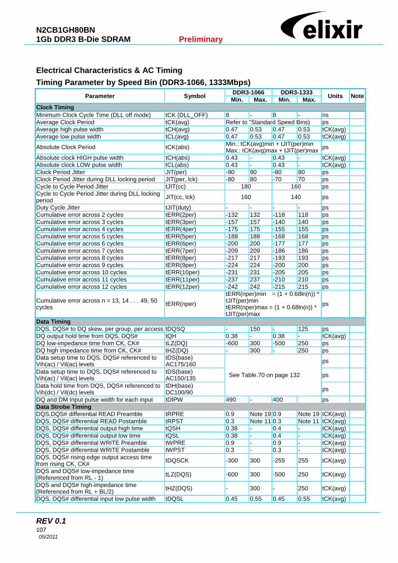
N2CB1GH80BN 1Gb DDR3 B-Die SDRAM Preliminary
REV 0.1 107 05/2011
Electrical Characteristics & AC Timing
Timing Parameter by Speed Bin (DDR3-1066, 1333Mbps)
Parameter Symbol DDR3-1066 DDR3-1333
Units Note Min. Max. Min. Max.
Clock Timing
Minimum Clock Cycle Time (DLL off mode) tCK (DLL_OFF) 8 - 8 - ns
Average Clock Period tCK(avg) Refer to "Standard Speed Bins) ps
Average high pulse width tCH(avg) 0.47 0.53 0.47 0.53 tCK(avg)
Average low pulse width tCL(avg) 0.47 0.53 0.47 0.53 tCK(avg)
Absolute Clock Period tCK(abs) Min.: tCK(avg)min + tJIT(per)min Max.: tCK(avg)max + tJIT(per)max
ps
Absolute clock HIGH pulse width tCH(abs) 0.43 - 0.43 - tCK(avg)
Absolute clock LOW pulse width tCL(abs) 0.43 - 0.43 - tCK(avg)
Clock Period Jitter JIT(per) -90 90 -80 80 ps
Clock Period Jitter during DLL locking period JIT(per, lck) -80 80 -70 70 ps
Cycle to Cycle Period Jitter tJIT(cc) 180 160 ps
Cycle to Cycle Period Jitter during DLL locking period
JIT(cc, lck) 160 140 ps
Duty Cycle Jitter tJIT(duty) - - - - ps
Cumulative error across 2 cycles tERR(2per) -132 132 -118 118 ps
Cumulative error across 3 cycles tERR(3per) -157 157 -140 140 ps
Cumulative error across 4 cycles tERR(4per) -175 175 -155 155 ps
Cumulative error across 5 cycles tERR(5per) -188 188 -168 168 ps
Cumulative error across 6 cycles tERR(6per) -200 200 -177 177 ps
Cumulative error across 7 cycles tERR(7per) -209 209 -186 186 ps
Cumulative error across 8 cycles tERR(8per) -217 217 -193 193 ps
Cumulative error across 9 cycles tERR(9per) -224 224 -200 200 ps
Cumulative error across 10 cycles tERR(10per) -231 231 -205 205 ps
Cumulative error across 11 cycles tERR(11per) -237 237 -210 210 ps
Cumulative error across 12 cycles tERR(12per) -242 242 -215 215 ps
Cumulative error across n = 13, 14 . . . 49, 50 cycles
tERR(nper)
tERR(nper)min = (1 + 0.68ln(n)) * tJIT(per)min tERR(nper)max = (1 + 0.68ln(n)) * tJIT(per)max
ps
Data Timing
DQS, DQS# to DQ skew, per group, per access tDQSQ - 150 - 125 ps
DQ output hold time from DQS, DQS# tQH 0.38 - 0.38 - tCK(avg)
DQ low-impedance time from CK, CK# tLZ(DQ) -600 300 -500 250 ps
DQ high impedance time from CK, CK# tHZ(DQ) - 300 - 250 ps
Data setup time to DQS, DQS# referenced to Vih(ac) / Vil(ac) levels
tDS(base) AC175/160
See Table.70 on page 132
ps
Data setup time to DQS, DQS# referenced to Vih(ac) / Vil(ac) levels
tDS(base) AC150/135
ps
Data hold time from DQS, DQS# referenced to Vih(dc) / Vil(dc) levels
tDH(base) DC100/90
ps
DQ and DM Input pulse width for each input tDIPW 490 - 400 ps
Data Strobe Timing
DQS,DQS# differential READ Preamble tRPRE 0.9 Note 19 0.9 Note 19 tCK(avg)
DQS, DQS# differential READ Postamble tRPST 0.3 Note 11 0.3 Note 11 tCK(avg)
DQS, DQS# differential output high time tQSH 0.38 - 0.4 - tCK(avg)
DQS, DQS# differential output low time tQSL 0.38 - 0.4 - tCK(avg)
DQS, DQS# differential WRITE Preamble tWPRE 0.9 - 0.9 - tCK(avg)
DQS, DQS# differential WRITE Postamble tWPST 0.3 - 0.3 - tCK(avg)
DQS, DQS# rising edge output access time from rising CK, CK#
tDQSCK -300 300 -255 255 tCK(avg)
DQS and DQS# low-impedance time (Referenced from RL - 1)
tLZ(DQS) -600 300 -500 250 tCK(avg)
DQS and DQS# high-impedance time (Referenced from RL + BL/2)
tHZ(DQS) - 300 - 250 tCK(avg)
DQS, DQS# differential input low pulse width tDQSL 0.45 0.55 0.45 0.55 tCK(avg)
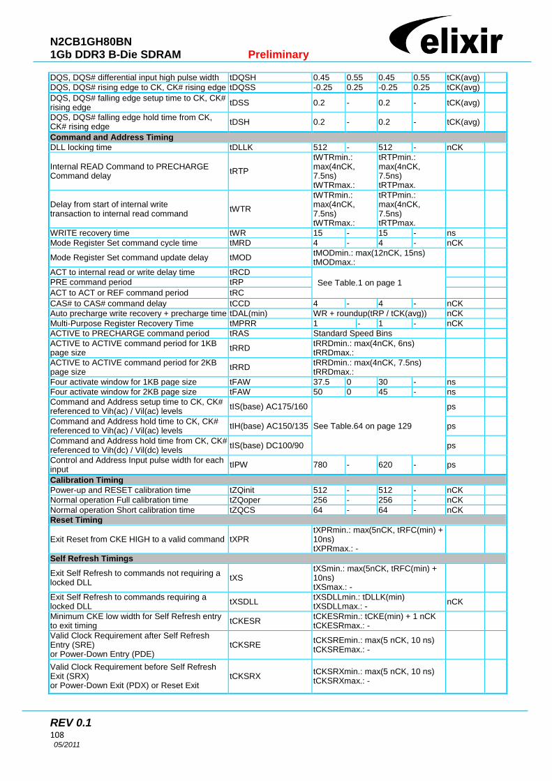
N2CB1GH80BN 1Gb DDR3 B-Die SDRAM Preliminary
REV 0.1 108 05/2011
DQS, DQS# differential input high pulse width tDQSH 0.45 0.55 0.45 0.55 tCK(avg)
DQS, DQS# rising edge to CK, CK# rising edge tDQSS -0.25 0.25 -0.25 0.25 tCK(avg)
DQS, DQS# falling edge setup time to CK, CK# rising edge
tDSS 0.2 - 0.2 - tCK(avg)
DQS, DQS# falling edge hold time from CK, CK# rising edge
tDSH 0.2 - 0.2 - tCK(avg)
Command and Address Timing
DLL locking time tDLLK 512 - 512 - nCK
Internal READ Command to PRECHARGE Command delay
tRTP
tWTRmin.: max(4nCK, 7.5ns) tWTRmax.:
tRTPmin.: max(4nCK, 7.5ns) tRTPmax.
Delay from start of internal write transaction to internal read command
tWTR
tWTRmin.: max(4nCK, 7.5ns) tWTRmax.:
tRTPmin.: max(4nCK, 7.5ns) tRTPmax.
WRITE recovery time tWR 15 - 15 - ns
Mode Register Set command cycle time tMRD 4 - 4 - nCK
Mode Register Set command update delay tMOD tMODmin.: max(12nCK, 15ns) tMODmax.:
ACT to internal read or write delay time tRCD See Table.1 on page 1
PRE command period tRP
ACT to ACT or REF command period tRC
CAS# to CAS# command delay tCCD 4 - 4 - nCK
Auto precharge write recovery + precharge time tDAL(min) WR + roundup(tRP / tCK(avg)) nCK
Multi-Purpose Register Recovery Time tMPRR 1 - 1 - nCK
ACTIVE to PRECHARGE command period tRAS Standard Speed Bins
ACTIVE to ACTIVE command period for 1KB page size
tRRD tRRDmin.: max(4nCK, 6ns) tRRDmax.:
ACTIVE to ACTIVE command period for 2KB page size
tRRD tRRDmin.: max(4nCK, 7.5ns) tRRDmax.:
Four activate window for 1KB page size tFAW 37.5 0 30 - ns
Four activate window for 2KB page size tFAW 50 0 45 - ns
Command and Address setup time to CK, CK# referenced to Vih(ac) / Vil(ac) levels
tIS(base) AC175/160
See Table.64 on page 129
ps
Command and Address hold time to CK, CK# referenced to Vih(ac) / Vil(ac) levels
tIH(base) AC150/135 ps
Command and Address hold time from CK, CK# referenced to Vih(dc) / Vil(dc) levels
tIS(base) DC100/90 ps
Control and Address Input pulse width for each input
tIPW 780 - 620 - ps
Calibration Timing
Power-up and RESET calibration time tZQinit 512 - 512 - nCK
Normal operation Full calibration time tZQoper 256 - 256 - nCK
Normal operation Short calibration time tZQCS 64 - 64 - nCK
Reset Timing
Exit Reset from CKE HIGH to a valid command tXPR tXPRmin.: max(5nCK, tRFC(min) + 10ns) tXPRmax.: -
Self Refresh Timings
Exit Self Refresh to commands not requiring a locked DLL
tXS tXSmin.: max(5nCK, tRFC(min) + 10ns) tXSmax.: -
Exit Self Refresh to commands requiring a locked DLL
tXSDLL tXSDLLmin.: tDLLK(min) tXSDLLmax.: -
nCK
Minimum CKE low width for Self Refresh entry to exit timing
tCKESR tCKESRmin.: tCKE(min) + 1 nCK tCKESRmax.: -
Valid Clock Requirement after Self Refresh Entry (SRE) or Power-Down Entry (PDE)
tCKSRE tCKSREmin.: max(5 nCK, 10 ns) tCKSREmax.: -
Valid Clock Requirement before Self Refresh Exit (SRX) or Power-Down Exit (PDX) or Reset Exit
tCKSRX tCKSRXmin.: max(5 nCK, 10 ns) tCKSRXmax.: -
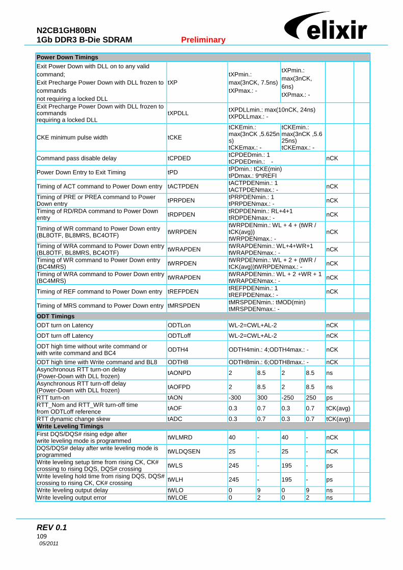
N2CB1GH80BN 1Gb DDR3 B-Die SDRAM Preliminary
REV 0.1 109 05/2011
Power Down Timings
Exit Power Down with DLL on to any valid
command;
Exit Precharge Power Down with DLL frozen to
commands
not requiring a locked DLL
tXP
tXPmin.:
max(3nCK, 7.5ns)
tXPmax.: -
tXPmin.:
max(3nCK,
6ns)
tXPmax.: -
Exit Precharge Power Down with DLL frozen to commands requiring a locked DLL
tXPDLL tXPDLLmin.: max(10nCK, 24ns) tXPDLLmax.: -
CKE minimum pulse width tCKE
tCKEmin.: max(3nCK ,5.625ns) tCKEmax.: -
tCKEmin.: max(3nCK ,5.625ns) tCKEmax.: -
Command pass disable delay tCPDED tCPDEDmin.: 1 tCPDEDmin.: -
nCK
Power Down Entry to Exit Timing tPD tPDmin.: tCKE(min) tPDmax.: 9*tREFI
Timing of ACT command to Power Down entry tACTPDEN tACTPDENmin.: 1 tACTPDENmax.: -
nCK
Timing of PRE or PREA command to Power Down entry
tPRPDEN tPRPDENmin.: 1 tPRPDENmax.: -
nCK
Timing of RD/RDA command to Power Down entry
tRDPDEN tRDPDENmin.: RL+4+1 tRDPDENmax.: -
nCK
Timing of WR command to Power Down entry (BL8OTF, BL8MRS, BC4OTF)
tWRPDEN tWRPDENmin.: WL + 4 + (tWR / tCK(avg)) tWRPDENmax.: -
nCK
Timing of WRA command to Power Down entry (BL8OTF, BL8MRS, BC4OTF)
tWRAPDEN tWRAPDENmin.: WL+4+WR+1 tWRAPDENmax.: -
nCK
Timing of WR command to Power Down entry (BC4MRS)
tWRPDEN tWRPDENmin.: WL + 2 + (tWR / tCK(avg))tWRPDENmax.: -
nCK
Timing of WRA command to Power Down entry (BC4MRS)
tWRAPDEN tWRAPDENmin.: WL + 2 +WR + 1 tWRAPDENmax.: -
nCK
Timing of REF command to Power Down entry tREFPDEN tREFPDENmin.: 1 tREFPDENmax.: -
nCK
Timing of MRS command to Power Down entry tMRSPDEN tMRSPDENmin.: tMOD(min) tMRSPDENmax.: -
ODT Timings
ODT turn on Latency ODTLon WL-2=CWL+AL-2 nCK
ODT turn off Latency ODTLoff WL-2=CWL+AL-2 nCK
ODT high time without write command or with write command and BC4
ODTH4 ODTH4min.: 4;ODTH4max.: - nCK
ODT high time with Write command and BL8 ODTH8 ODTH8min.: 6;ODTH8max.: - nCK
Asynchronous RTT turn-on delay (Power-Down with DLL frozen)
tAONPD 2 8.5 2 8.5 ns
Asynchronous RTT turn-off delay (Power-Down with DLL frozen)
tAOFPD 2 8.5 2 8.5 ns
RTT turn-on tAON -300 300 -250 250 ps
RTT_Nom and RTT_WR turn-off time from ODTLoff reference
tAOF 0.3 0.7 0.3 0.7 tCK(avg)
RTT dynamic change skew tADC 0.3 0.7 0.3 0.7 tCK(avg)
Write Leveling Timings
First DQS/DQS# rising edge after write leveling mode is programmed
tWLMRD 40 - 40 - nCK
DQS/DQS# delay after write leveling mode is programmed
tWLDQSEN 25 - 25 - nCK
Write leveling setup time from rising CK, CK# crossing to rising DQS, DQS# crossing
tWLS 245 - 195 - ps
Write leveling hold time from rising DQS, DQS# crossing to rising CK, CK# crossing
tWLH 245 - 195 - ps
Write leveling output delay tWLO 0 9 0 9 ns
Write leveling output error tWLOE 0 2 0 2 ns
N2CB1GH80BN 1Gb DDR3 B-Die SDRAM Preliminary
REV 0.1 110 05/2011
Jitter Notes
Specific Note a
Unit “tCK(avg)” represents the actual tCK(avg) of the input clock under operation. Unit “nCK” represents one clock cycle
of the input clock, counting the actual clock edges. ex) tMRD=4 [nCK] means; if one Mode Register Set command is
registered at Tm, anther Mode Register Set command may be registered at Tm+4, even if (Tm+4-Tm) is 4 x tCK(avg) +
tERR(4per), min.
Specific Note b
These parameters are measured from a command/address signal (CKE, , , , , ODT, BA0, A0, A1, etc)
transition edge to its respective clock signal (CK/) crossing. The spec values are not affected by the amount of clock
jitter applied (i.e. tJIT(per), tJIT(cc), etc.), as the setup and hold are relative to the clock signal crossing that latches the
command/address. That is, these parameters should be met whether clock jitter is present or not.
Specific Note c
These parameters are measured from a data strobe signal (DQS(L/U), )) crossing to its respective clock signal
(CK, ) crossing. The spec values are not affected by the amount of clock jitter applied (i.e. tJIT(per), tJIT(cc), etc), as
these are relative to the clock signal crossing. That is, these parameters should be met whether clock jitter is present or
not.
Specific Note d
These parameters are measured from a data signal (DM(L/U), DQ(L/U)0, DQ(L/U)1, etc.) transition edge to its respective
data strobe signal (DQS(L/U), ) crossing.
Specific Note e
For these parameters, the DDR3 SDRAM device supports tnPARAM [nCK] = RUtPARAM[ns] / tCK(avg)[ns], which is in
clock cycles, assuming all input clock jitter specifications are satisfied. For example, the device will support tnRP =
RUtRP/tCK(avg), which is in clock cycles, if all input clock jitter specifications are met. This means: For DDR3-1066
7-7-7, of which tRP = 13.125ns, the device will support tnRP = RUtRP/tCK(avg) = 7, as long as the input clock jitter
specifications are met, i.e. Precharge command at Tm and Active command at Tm+7 is valid even if (Tm+7-Tm) is less
than 13.125ns due to input clock jitter.
Specific Note f
When the device is operated with input clock jitter, this parameter needs to be derated by the actual tERR(mper), act of
the input clock, where 2 <= m <=12. (Output derating is relative to the SDRAM input clock.)
Specific Note g
When the device is operated with input clock jitter, this parameter needs to be derated by the actual tJIT(per),act of the
input clock. (Output deratings are relative to the SDRAM input clock.)

N2CB1GH80BN 1Gb DDR3 B-Die SDRAM Preliminary
REV 0.1 111 05/2011
Timing Parameter Notes
1. Actual value dependent upon measurement level definitions which are TBD.
2. Commands requiring a locked DLL are: READ ( and RAP) are synchronous ODT commands.
3. The max values are system dependent.
4. WR as programmed in mode register.
5. Value must be rouned-up to next higher integer value.
6. There is no maximum cycle time limit besides the need to satisfy the refresh interval, tREFI.
7. For definition of RTT-on time tAON See “Timing Parameters”.
8. For definition of RTT-off time tAOF See “Timing Parameters”.
9. tWR is defined in ns, for calculation of tWRPDEN it is necessary to round up tWR / tCK to the next integer.
10. WR in clock cycles are programmed in MR0.
11. The maximum read postamble is bounded by tDQSCK(min) plus tQSH(min) on the left side and tHZ(DQS)max on the
right side.
12. Output timing deratings are relative to the SDRAM input clock. When the device is operated with input clock jitter, this
parameter needs to be derated by TBD.
13. Value is only valid for RON34.
14. Single ended signal parameter.
15. tREFI depends on TOPER.
16. tIS(base) and tIH(base) values are for 1V/ns CMD/ADD single-ended slew rate and 2V/ns CK, CK differential slew
rate. Note for DQ and DM signals, VREF(DC)=VRefDQ(DC). For input only pins except RESET,
VRef(DC)=VRefCA(DC).
17. tDS(base) and tDH(base) values are for 1V/ns DQ single-ended slew rate and 2V/ns DQS, DQS differential slew rate.
Note for DQ and DM signals, VREF(DC)=VRefDQ(DC). For input only pins except RESET, VRef(DC)=VRefCA(DC).
18. Start of internal write transaction is defined as follows:
For BL8 (fixed by MRS and on-the-fly): Rising clock edge 4 clock cycles after WL.
For BC4 (on-the-fly): Rising clock edge 4 clock cycles after WL.
For BC4 (fixed by MRS): Rising clock edge 2 clock cycles after WL.
19. The maximum preamble is bound by tLZ (DQS) max on the left side and tDQSCK(max) on the right side.
20. CKE is allowed to be registered low while operations such as row activation, precharge, autoprecharge or refresh are
in progress, but power-down IDD spec will not be applied until finishing those operations.
21. Although CKE is allowed to be registered LOW after a REFRESH command once tREFPDEN (min) is satisfied, there
are cases where additional time such as tXPDLL (min) is also required.
22. Defined between end of MPR read burst and MRS which reloads MPR or disables MPR function.
23. One ZQCS command can effectively correct a minimum of 0.5% (ZQCorrection) of RON and RTT impedance error
within 64 nCK for all speed bins assuming the maximum sensitivities specified in the “Output Driver Voltage and
Temperature Sensitivity” and “ODT Voltage and Temperature Sensitivity” tables. The appropriate interval between
ZQCS commands can be determined from these tables and other application-specific parameters.One method for
calculating the interval between ZQCS commands, given the temperature (Tdriftrate) and voltage (Vdriftrate) drift
rates that the SDRAM is subject to in the application, is illustrated. the interval could be defined by the following
formula: ZQCorrection / [(TSens x Tdriftrate) + (VSens x Vdriftrate)] where TSens = max(dRTTdT, dRONdTM) and
VSens = max(dRTTdV, dRONdVM) define the SDRAM temperature and voltage sensitivities. For example, if TSens =
1.5%/C, VSens = 0.15%/mV, Tdriftrate = 1 C/sec and Vdriftrate = 15mV/sec, then the interval between ZQCS
commands is calculated as 0.5 / [(1.5x1)+(0.15x15)] = 0.133 ~ 128ms
24. n = from 13 cycles to 50 cycles. This row defines 38 parameters.
25. tCH(abs) is the absolute instantaneous clock high pulse width, as measured from one rising edge to the following

N2CB1GH80BN 1Gb DDR3 B-Die SDRAM Preliminary
REV 0.1 112 05/2011
falling edge.
26. tCL(abs) is the absolute instantaneous clock low pulse width, as measured from one falling edge to the following rising
edge.
27. The tIS(base) AC150 specifications are adjusted from the tIS(base) specification by adding an additional 100ps of
derating to accommodate for the lower altemate threshold of 150mV and another 25ps to account for the earlier
reference point [(175mV - 150mV) / 1V/ns].

N2CB1GH80BN 1Gb DDR3 B-Die SDRAM Preliminary
REV 0.1 113 05/2011
Address / Command Setup, Hold, and Derating
For all input signals the total tIS (setup time) and tIH (hold time) required is calculated by adding the data sheet tIS(base)
and tIH(base) and tIH(base) value to the delta tIS and delta tIH derating value respectively.
Example: tIS (total setup time) = tIS(base) + delta tIS
Setup (tIS) nominal slew rate for a rising signal is defined as the slew rate between the last crossing of Vref(dc) and the first
crossing of VIH(ac)min. Setup (tIS) nominal slew rate for a falling signal is defined as the slew rate between the last
crossing of Vref(dc) and the first crossing of VIL(ac)max. If the actual signal is always earlier than the nominal slew rate line
between shaded „Vref(dc) to ac region‟, use nominal slew rate for derating value. If the actual signal is later than the
nominal slew rate line anywhere between shaded „Vref(dc) to ac region‟, the slew rate of the tangent line to the actual signal
from the ac level to dc level is used for derating value.
Hold (tIH) nominal slew rate for a rising signal is defined as the slew rate between the last crossing of VIL(dc)max and the
first crossing of Vref(dc). Hold (tIH) nominal slew rate for a falling signal is defined as the slew rate between the last
crossing of VIH(dc)min and the first crossing of Vref(dc). If the actual signal is always later than the nominal slew rate line
between shaded „dc to Vref(dc) region‟, use nominal slew rate for derating value. If the actual signal is earlier than the
nominal slew rate line anywhere between shaded „dc to Vref(dc) region‟, the slew rate of a tangent line to the actual signal
from the dc level to Vref(dc) level is used for derating value. For a valid transition the input signal has to remain
above/below VIH/IL(ac) for some time tVAC. Although for slow slew rates the total setup time might be negative (i.e. a valid
input signal will not have reached VIH/IL(ac) at the time of the rising clock transition) a valid input signal is still required to
complete the transition and reach VIH/IL(ac).
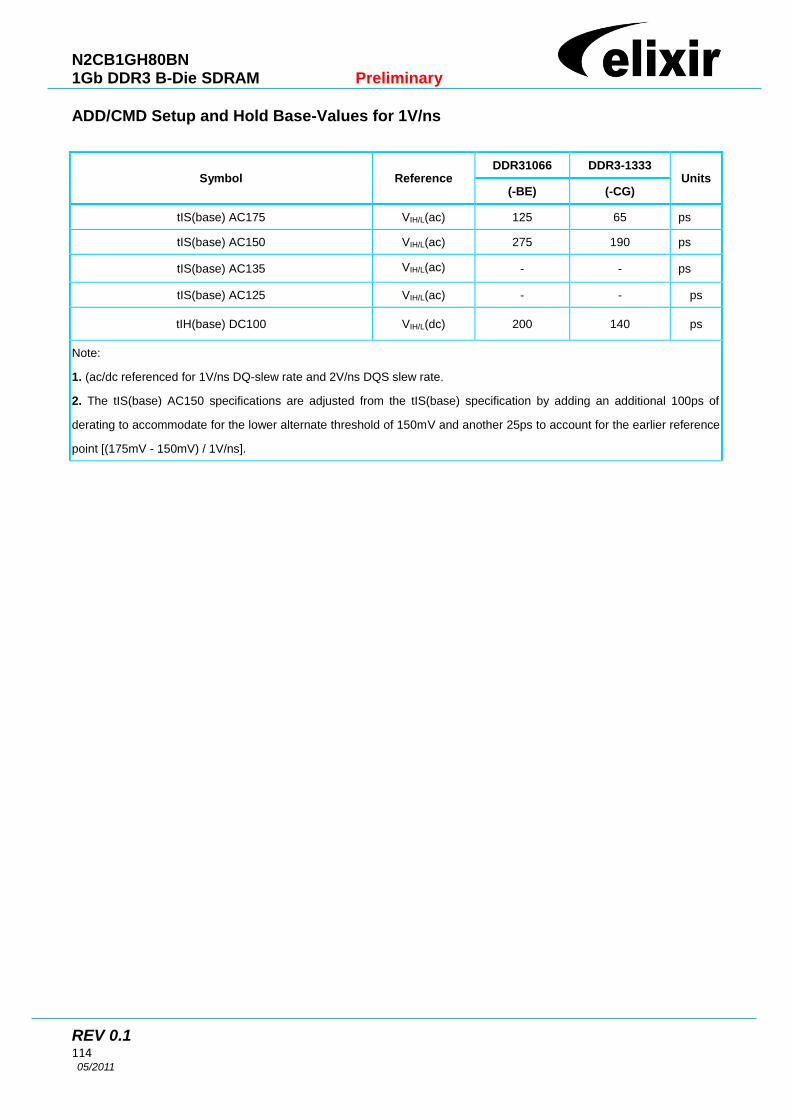
N2CB1GH80BN 1Gb DDR3 B-Die SDRAM Preliminary
REV 0.1 114 05/2011
ADD/CMD Setup and Hold Base-Values for 1V/ns
Symbol Reference DDR31066 DDR3-1333
Units (-BE) (-CG)
tIS(base) AC175 VIH/L(ac) 125 65 ps
tIS(base) AC150 VIH/L(ac) 275 190 ps
tIS(base) AC135 VIH/L(ac) - - ps
tIS(base) AC125 VIH/L(ac) - - ps
tIH(base) DC100 VIH/L(dc) 200 140 ps
Note:
1. (ac/dc referenced for 1V/ns DQ-slew rate and 2V/ns DQS slew rate.
2. The tIS(base) AC150 specifications are adjusted from the tIS(base) specification by adding an additional 100ps of
derating to accommodate for the lower alternate threshold of 150mV and another 25ps to account for the earlier reference
point [(175mV - 150mV) / 1V/ns].
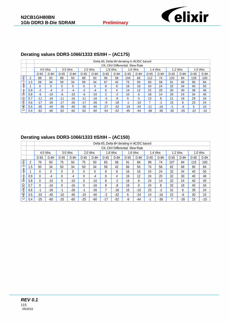
N2CB1GH80BN 1Gb DDR3 B-Die SDRAM Preliminary
REV 0.1 115 05/2011
Derating values DDR3-1066/1333 tIS/tIH – (AC175)
Derating values DDR3-1066/1333 tIS/tIH – (AC150)
D tIS D tIH D tIS D tIH D tIS D tIH D tIS D tIH D tIS D tIH D tIS D tIH D tIS D tIH D tIS D tIH
2 88 50 88 50 88 50 96 58 104 66 112 74 120 84 128 100
1.5 59 34 59 34 59 34 67 42 75 50 83 58 91 68 99 84
1 0 0 0 0 0 0 8 8 16 16 24 24 32 34 40 50
0.9 -2 -4 -2 -4 -2 -4 6 4 14 12 22 20 30 30 38 46
0.8 -6 -10 -6 -10 -6 -10 2 -2 10 6 18 14 26 24 34 40
0.7 -11 -16 -11 -16 -11 -16 -3 -8 5 0 13 8 21 18 29 34
0.6 -17 -26 -17 -26 -17 -26 -9 -18 -1 -10 7 -2 15 8 23 24
0.5 -35 -40 -35 -40 -35 -40 -27 -32 -19 -24 -11 -16 -2 -6 5 10
0.4 -62 -60 -62 -60 -62 -60 -54 -52 -46 -44 -38 -36 -30 -26 -22 -10
Delta tIS, Delta tIH derating in AC/DC based
2.0 V/ns 1.8 V/ns 1.6 V/ns 1.4 V/ns 1.0 V/ns1.2 V/ns
CM
D/A
DD
Sle
w r
ate
(V
/ns)
4.0 V/ns 3.0 V/ns
CK, CK# Differential Slew Rate
D tIS D tIH D tIS D tIH D tIS D tIH D tIS D tIH D tIS D tIH D tIS D tIH D tIS D tIH D tIS D tIH
2 75 50 75 50 75 50 83 58 91 66 99 74 107 84 115 100
1.5 50 34 50 34 50 34 58 42 66 50 74 58 82 68 90 84
1 0 0 0 0 0 0 8 8 16 16 24 24 32 34 40 50
0.9 0 -4 0 -4 0 -4 8 4 16 12 24 20 32 30 40 46
0.8 0 -10 0 -10 0 -10 8 -2 16 6 24 14 32 24 40 40
0.7 0 -16 0 -16 0 -16 8 -8 16 0 24 8 32 18 40 34
0.6 -1 -26 -1 -26 -1 -26 7 -18 15 -10 23 -2 31 8 39 24
0.5 -10 -40 -10 -40 -10 -40 -2 -32 6 -24 14 -16 22 -6 30 10
0.4 -25 -60 -25 -60 -25 -60 -17 -52 -9 -44 -1 -36 7 -26 15 -10CM
D/A
DD
Sle
w r
ate
(V
/ns)
4.0 V/ns 3.0 V/ns
CK, CK# Differential Slew Rate
Delta tIS, Delta tIH derating in AC/DC based
2.0 V/ns 1.8 V/ns 1.6 V/ns 1.4 V/ns 1.0 V/ns1.2 V/ns

N2CB1GH80BN 1Gb DDR3 B-Die SDRAM Preliminary
REV 0.1 116 05/2011
Required time tVAC above VIH(ac) below VIL(ac) for valid transition
Slew Rate [V/ns] tVAC@175mV [ps] tVAC@175mV [ps]
min max min max
>2.0 75 - 175 -
2 57 - 170 -
1.5 50 - 167 -
1 38 - 163 -
0.9 34 - 162 -
0.8 29 - 161 -
0.7 22 - 159 -
0.6 13 - 155 -
0.5 0 - 150 -
<0.5 0 - 150 -

N2CB1GH80BN 1Gb DDR3 B-Die SDRAM Preliminary
REV 0.1 117 05/2011
Data Setup, Hold, and Slew Rate De-rating
For all input signals the total tDS (setup time) and tDH (hold time) required is calculated by adding the data sheet tDH(base)
and tDH(base) value to the delta tDS and delta tDH derating value respectively.
Example: tDS (total setup time) = tDS(base) + delta tDS
Setup (tDS) nominal slew rate for a rising signal is defined as the slew rate between the last crossing of Vref(dc) and the
first crossing of VIH(ac)min. Setup (tDS) nominal slew rate for a falling signal is defined as the slew rate between the last
crossing of Vref(dc) and the first crossing of VIL(ac)max. If the actual signal is always earlier than the nominal slew rate line
between shaded „Vref(dc) to ac region‟, use nominal slew rate for derating value. If the actual signal is later than the
nominal slew rate line anywhere between shaded „Vref(dc) to ac region‟, the slew rate of the tangent line to the actual signal
from the ac level to dc level is used for derating value.
Hold (tDH) nominal slew rate for a rising signal is defined as the slew rate between the last crossing of VIL(dc)max and the
first crossing of Vref(dc). Hold (tDH) nominal slew rate for a falling signal is defined as the slew rate between the last
crossing of VIH(dc)min and the first crossing of Vref(dc). If the actual signal is always later than the nominal slew rate line
between shaded „dc level to Vref(dc) region‟, use nominal slew rate for derating value. If the actual signal is earlier than the
nominal slew rate line anywhere between shaded „dc to Vref(dc) region‟, the slew rate of a tangent line to the actual signal
from the dc level to Vref(dc) level is used for derating value.
For a valid transition the input signal has to remain above/below VIH/IL(ac) for some time tVAC.
Although for slow slew rates the total setup time might be negative (i.e. a valid input signal will not have reached VIH/IL(ac)
at the time of the rising clock transition) a valid input signal is still required to complete the transition and reach VIH/IL(ac).
For slew rates in between the values listed in the following tables, the derating values may be obtained by linear
interpolation.
These values are typically not subject to production test. They are verified by design and characterization.
Data Setup and Hold Base-Values
Unit [ps] reference DDR3-1066 DDR3-1333 Units
tDS(base)AC175 VIH/L(ac) 25 - ps
tDS(base)AC150 VIH/L(ac) 75 30 ps
tDS(base)AC135 VIH/L(ac) - - ps
tDH(base)DC100 VIH/L(dc) 100 65 ps
Note: ac/dc referenced for 1V/ns DQ-slew rate and 2V/ns DQS slew rate
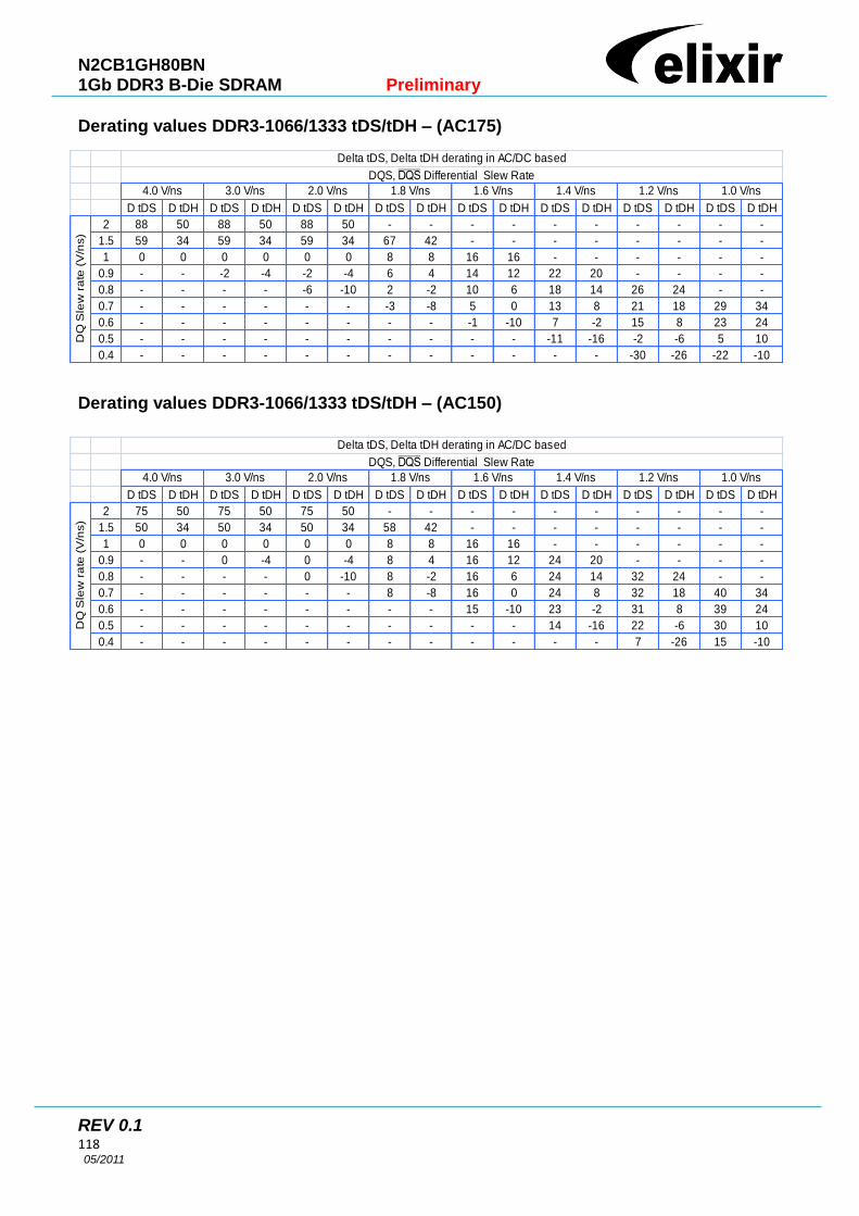
N2CB1GH80BN 1Gb DDR3 B-Die SDRAM Preliminary
REV 0.1 118 05/2011
Derating values DDR3-1066/1333 tDS/tDH – (AC175)
Derating values DDR3-1066/1333 tDS/tDH – (AC150)
D tDS D tDH D tDS D tDH D tDS D tDH D tDS D tDH D tDS D tDH D tDS D tDH D tDS D tDH D tDS D tDH
2 88 50 88 50 88 50 - - - - - - - - - -
1.5 59 34 59 34 59 34 67 42 - - - - - - - -
1 0 0 0 0 0 0 8 8 16 16 - - - - - -
0.9 - - -2 -4 -2 -4 6 4 14 12 22 20 - - - -
0.8 - - - - -6 -10 2 -2 10 6 18 14 26 24 - -
0.7 - - - - - - -3 -8 5 0 13 8 21 18 29 34
0.6 - - - - - - - - -1 -10 7 -2 15 8 23 24
0.5 - - - - - - - - - - -11 -16 -2 -6 5 10
0.4 - - - - - - - - - - - - -30 -26 -22 -10
1.2 V/ns
DQ
Sle
w r
ate
(V
/ns)
4.0 V/ns 3.0 V/ns
DQS, Differential Slew Rate
Delta tDS, Delta tDH derating in AC/DC based
2.0 V/ns 1.8 V/ns 1.6 V/ns 1.4 V/ns 1.0 V/ns
D tDS D tDH D tDS D tDH D tDS D tDH D tDS D tDH D tDS D tDH D tDS D tDH D tDS D tDH D tDS D tDH
2 75 50 75 50 75 50 - - - - - - - - - -
1.5 50 34 50 34 50 34 58 42 - - - - - - - -
1 0 0 0 0 0 0 8 8 16 16 - - - - - -
0.9 - - 0 -4 0 -4 8 4 16 12 24 20 - - - -
0.8 - - - - 0 -10 8 -2 16 6 24 14 32 24 - -
0.7 - - - - - - 8 -8 16 0 24 8 32 18 40 34
0.6 - - - - - - - - 15 -10 23 -2 31 8 39 24
0.5 - - - - - - - - - - 14 -16 22 -6 30 10
0.4 - - - - - - - - - - - - 7 -26 15 -10
1.0 V/ns1.2 V/ns
DQ
Sle
w r
ate
(V
/ns)
4.0 V/ns 3.0 V/ns
DQS, Differential Slew Rate
Delta tDS, Delta tDH derating in AC/DC based
2.0 V/ns 1.8 V/ns 1.6 V/ns 1.4 V/ns

N2CB1GH80BN 1Gb DDR3 B-Die SDRAM Preliminary
REV 0.1 119 05/2011
Required time tVAC above VIH(ac) below VIL(ac) for valid transition
Slew Rate [V/ns]
DDR3-1066 (AC175) DDR3-1333 (AC150)
tVAC[ps] tVAC[ps]
Min. Max. Min. Max.
>2.0 75 - 175 -
2 57 - 170 -
1.5 50 - 167 -
1 38 - 163 -
0.9 34 - 162 -
0.8 29 - 161 -
0.7 22 - 159 -
0.6 13 - 155 -
0.5 0 - 155 -
<0.5 0 - 150 -
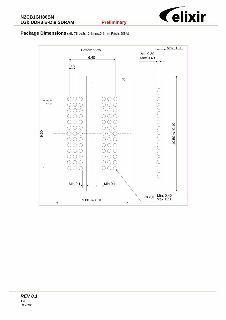
N2CB1GH80BN 1Gb DDR3 B-Die SDRAM Preliminary
REV 0.1 120 05/2011
Package Dimensions (x8; 78 balls; 0.8mmx0.8mm Pitch; BGA)
Min 0.30
Max 0.40
Max. 1.20
9.6
0
0.8
0.8
6.40
Bottom View
10
.50
+/-
0.1
0
9.00 +/- 0.1078 x o
Max. 0.50Min. 0.40
Min 0.1 Min 0.1
N2CB1GH80BN 1Gb DDR3 B-Die SDRAM Preliminary
REV 0.1 121 05/2011
Revision Log
Rev Date Modification
0.1 05/2011 Preliminary Release