nanostructures fabricated by physical techniques
TRANSCRIPT

Nanostructures fabricated by physical techniques
Physical fabrication techniques (Top-down methods) forproducing nanostructures are derived mainly from the techniquesapplied for the fabrication of microstructures in semiconductorindustry.
The main techniques that will be illustrated are:
(1) Lithographic techniques
(2) Nanomanipulation and nanolithography
(3) Soft lithography
(4) Self-assembly of nanoparticles or nanowires

Lithography
Lithography is the process of transferring a pattern into areactive polymer film, termed as resist, which willsubsequently be used to replicate that pattern into anunderlying thin film or substrate.
Many techniques of lithography have been developed in the lasthalf a century with various lens systems and exposure radiationsources including photons, X-rays, electrons, ions andneutral atoms.
Photolithography is the most widely used technique inmicroelectronic fabrication, particularly for mass production ofintegrated circuit.

PhotolithographyTypical photolithographic process consists of producing a maskcarrying the requisite pattern information and subsequentlytransferring that pattern, using some optical technique into aphotoactive polymer or photoresist (or simply resist).There are two basic photolithographic approaches:
(i) Shadow printing, which can be further divided into contactprinting (or contact-mode printing) and proximity printing
(ii) Projection printing.
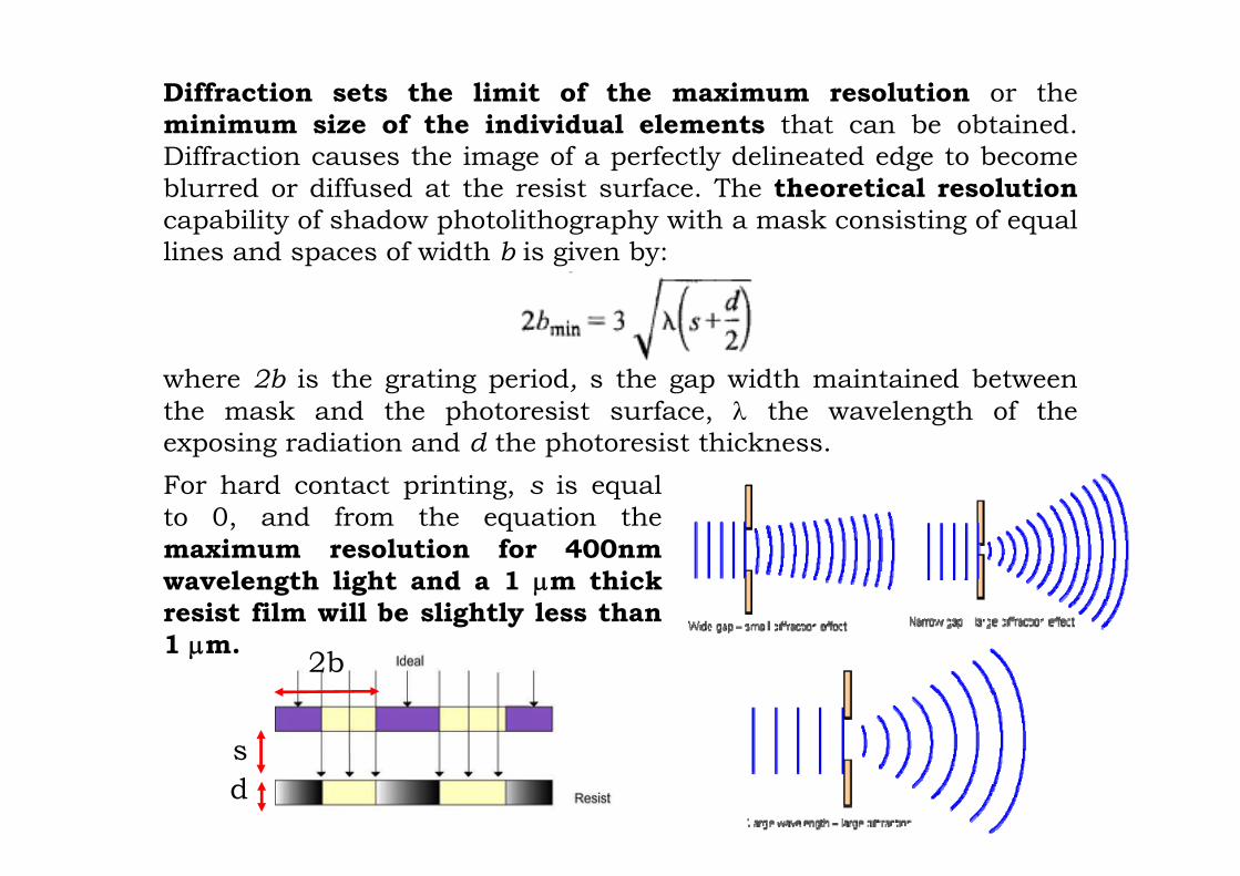
Diffraction sets the limit of the maximum resolution or theminimum size of the individual elements that can be obtained.Diffraction causes the image of a perfectly delineated edge to becomeblurred or diffused at the resist surface. The theoretical resolutioncapability of shadow photolithography with a mask consisting of equallines and spaces of width b is given by:
where 2b is the grating period, s the gap width maintained betweenthe mask and the photoresist surface, the wavelength of theexposing radiation and d the photoresist thickness.
s
2b
d
For hard contact printing, s is equalto 0, and from the equation themaximum resolution for 400nmwavelength light and a 1 m thickresist film will be slightly less than1 m.

In contact-mode photolithography, the mask and wafer are inintimate contact, and thus almost 100% of accuracy is reached andthis method provides the highest resolution. However, themaximum resolution is seldom achieved because of dust onsubstrates and non-uniformity of the thickness of thephotoresist and the substrate.
These problems can be avoided in proximity printing, in which, agap between the mask and the wafer is introduced. However,increasing the gap degrades the resolution by expanding thepenumbral region caused by diffraction. The main difficulties inproximity printing are the control of a small and very constantspace between the mask and wafer, which can be achieved onlywith extremely flat wafers and masks.
s
2b
d
Shadow printing

Projection printing differsfrom shadow printing. Inprojection printingtechniques, lens elementsare used to focus the maskimage onto a wafersubstrate, which isseparated from the mask bymany centimeters.
Projection techniquesgenerally have lowerresolution capability thanthat provided by shadowprinting due to lensimperfections and diffractionconsiderations.
Projection printing

The resolution, i.e. the minimum resolvable feature R and thecorresponding depth of focus (DOF) are given by:
Where is the exposure wavelength, k1 and k2 are constants that depend on thespecific resist material, process technology and image-formation techniques used,and NA is the numerical aperture of the optical system, with n refractive indexof the image space (usually air) and the maximum cone angle of the exposurelight beam.
Best resolution are of the order of /2 and in general conventionalphotolithography is capable of fabricating features of at least 200nm. To obtain higher resolutions, shorter wavelength and lens systemswith larger numerical apertures should be used.Deep UV lithography (DUV) based on exposure at wavelengths below 300nm (Excimer lasers) can be used. DUV lithography allows one to obtainpatterns with a minimal size of about 100 nm.Extreme UV (EUV) lithography with wavelengths in the range of 11-13nm can be used for fabricating features with even smaller dimensions andis a strong candidate for achieving dimensions of 70nm and below.Main problem is the strong absorption of light at these wavelengths.

Basic imaging characteristics (a) Ideal shadow imaging; (b) Diffraction-broadened projection imaging

Photolithographic methods
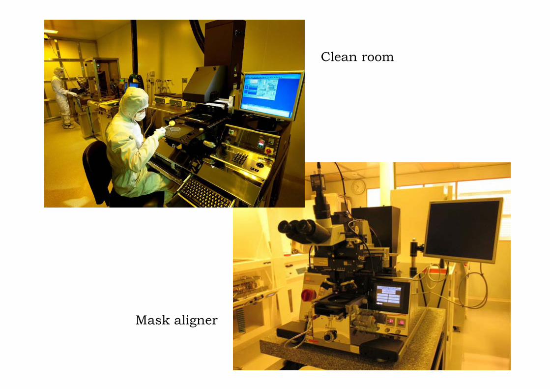
Mask aligner
Clean room

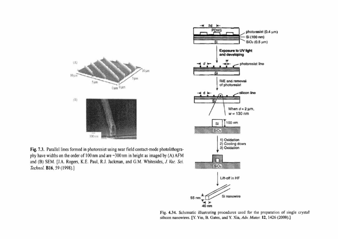
Phase-shifting photolithographyIn this method, a transparent mask induces abrupt changes ofthe phase of the light used for exposure, and cause opticalattenuation at desired locations. These phase masks, also knownas phase shifters, can produce features of about 100 nm inphotoresist.By introducing elastomeric phase-shifting masks, conformal contactcan be relatively easily achieved and feature lines as narrow as50nm can be generated. The resolution achieved correspondsapproximately to /5.An improved approach to conformal near field photolithography is touse masks constructed from ‘‘soft” organic elastomeric polymers.


An example of resolution enhancement technology and the effect of phase shifting technology

Electron beam lithography (EBL)A finely focused beam of electrons canbe deflected accurately and preciselyover a surface. When the surface iscoated with a radiation sensitivepolymeric material, the electronbeam can be used to write patterns ofvery high resolution.Electron beams can be focused to a fewnanometers in diameter and rapidlydeflected either electromagnetically orelectrostatically. Electrons possess bothparticle and wave properties; however,their wavelength is of the order of a fewtenths of angstrom, and therefore theirresolution is not limited bydiffraction considerations.Resolution of electron beam lithography is, however, limited byforward scattering of the electrons in the resist layer and backscattering from the underlying substrate. Nevertheless, electron beamlithography is the most powerfull tool for the fabrication of structures assmall as 3-5 nm.
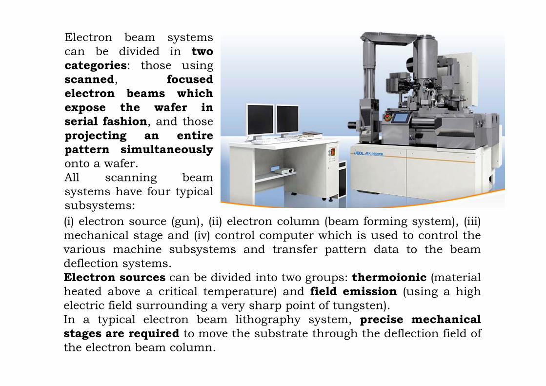
(i) electron source (gun), (ii) electron column (beam forming system), (iii)mechanical stage and (iv) control computer which is used to control thevarious machine subsystems and transfer pattern data to the beamdeflection systems.Electron sources can be divided into two groups: thermoionic (materialheated above a critical temperature) and field emission (using a highelectric field surrounding a very sharp point of tungsten).In a typical electron beam lithography system, precise mechanicalstages are required to move the substrate through the deflection field ofthe electron beam column.
Electron beam systemscan be divided in twocategories: those usingscanned, focusedelectron beams whichexpose the wafer inserial fashion, and thoseprojecting an entirepattern simultaneouslyonto a wafer.All scanning beamsystems have four typicalsubsystems:


Photolithography vs e-beam lithography

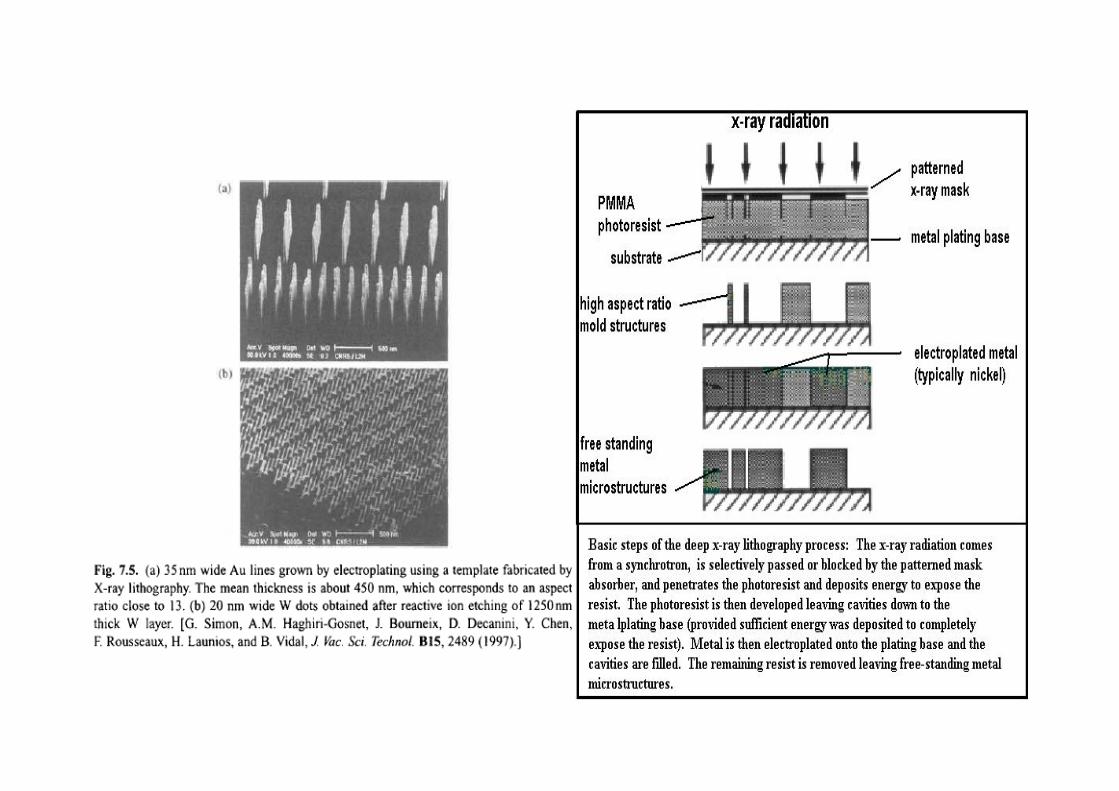
X-ray lithographyX-rays with wavelengths in the range of 0.04 to 0.5 nm (31 KeV-2.5 KeV) represent another alternative radiation source withpotential for high-resolution pattern replication into polymeric resistmaterials.The essential ingredients in X-ray lithography include:(1) A mask consisting of a pattern made with an X-ray absorbing
material on a thin X-ray transparent membrane(2) An X-ray source of sufficient brightness in the wavelengthrange of interest to expose the resist through the mask(3) An X-ray sensitive resist material.
X-ray radiation sources: (i) electron impact and (ii) synchrotronsources.Absorption of an X-ray photon results in the formation of aphotoelectron which undergoes elastic and inelastic collisionswithin the absorbing material producing secondary electronswhich are responsible for the chemical reactions in the resist film.The range of the primary photoelectrons is on the order of 100-200nm. The resolution limit of the X-ray lithography is about 25 nm.

Ion beam lithographyIon beam lithography (IBL) is the practice ofscanning a focused beam of ions in apatterned fashion across a surface tofabricate nanostructures.Advantages are the lack of backscatteredelectrons and higher resolution than theother techniques.
Ion sources (H, He, Ga,…)
-Focused IBL (direct writing)-Masked IBL (beam passes through ion-transparent membrane patterned withasbsorbing material)

