nanostructures by anne simon moffat - · pdf filenanostructures by anne simon moffat ......
TRANSCRIPT

NANOSTRUCTURES
by Anne Simon Moffat
n April 1990, researchers at the IBM Almaden Research Center in San
' Jose, California, gave new meaning . to the concept of tight graphic de
sign. Using the magnetic pull on the tip of a scanning tunneling microscope to drag atoms of xenon across a crystal of nickel, Donald M. Eigler and E. K. Schweizer built up an IBM logo, one atom at a time. Each letter measured five nanometers (five billionths of a meter) from top to bottom, and each xenon atom appeared as a 0.16-nanometer bump on the crystal surface. It took 9 atoms to make the /, 13 for the B, and 13 for the M. This achievement is the latest in a recent series of efforts to design, build, test, and manipulate structures on the scale of nanometers.
Ten years ago, the construction of devices with a minimum feature size of one micrometer was considered an achievement, and within the last five years, construction of devices down to 0.1 micrometer in size became commonplace. Now, research at IBM and elsewhere suggests that, during the 1990s, manipulations on the order of a few billionths of a meter or less will become routine in the best-equipped laboratories. Electronics manufacturers are hopeful that, by the turn of the century, nanofabrication technologies will enable them to mass-produce integrated circuits with a minimum feature size as small as 25 nanometers.
Before the products of nanofabrication reach the market, considerably more basic knowledge must be gained. More is now known about how to build ultrasmall structures, for example, than about their quirky behaviors. The IBM masterpiece falls apart when temperatures rise above minus 380 degrees Fahrenheit. Both the usefulness of reduced
size and the need to understand the behavior of matter at the finest of resolutions continue to spur the research.
John Cowley, an authority on imaging systems at Arizona State University, who is working to build a refined electron microscope that will push its resolution from 0.16 nanometer to 0.1 nanometer, says there is a limit to the scale at which useful information can be gained. "It is determined by the distance between atoms, that is, 0.08 to 0.1 nanometer," says Cowley. 'There is not much point in going below 0.05 nanometer for useful information, although there is a lot to be gained from going from 0.2 to 0.1 nanometer; this allows you to identify the individual atoms that form chemical bonds."
Similarly, Evelyn Hu, a fabrication specialist at the University of California at Santa Barbara, feels that "much can be learned by techniques that allow the manipulation of matter at 0.2 to 0.3 nanometer, a scale that reflects the routine fluctuations of atoms." At this point in efforts to go from a few tens of a nanometer to a few tenths of a nanometer, she says, "science is more limited by human ingenuity than by any hard-and-fast physical barriers."
Strange behavior
The lure of the study of matter on the scale of 10"9 meter or less is strong. Nanoscale structures offer an especially good opportunity to test key concepts of quantum physics.
The first such structures, built about ten years ago, proved to be more than miniaturized versions of larger ones. At a scale between millionths and billionths of a meter, new and intriguing phenomena appeared. Electrons no
longer acted as discrete parang -v-ii: precise positions. Instead, as the dimensions of electronic devices shrank into the nanorealm, quantum effects emerged; electrons behaved more like waves whose positions are described as a probabilistic fuzz, and they tunneled through barriers.
Moreover, it has become evident within the last year or two that electronics is not the only field to witness strange new behavior at very small dimensions. Physicists and engineers studying optics have noticed novel, nonlinear effects. So have those studying mechanical properties. For example, classical laws of friction, stress, and fatigue are upset in devices built on the scale of micrometers. Thus, as engineers have shrank devices, whole new areas of science have been opened to exploration.
30 MOSAIC Volume 21 Number 4 Winter 1990
n April 1990, researchers at the IBM Almaden Research Center in San Jose? California, gave new meaning to the concept of tight graphic de-

The fabrication and study of structures measured in ten-billionths of a meter
challenge all known lithographic techniques, advancing, along with technology,
understanding of the quantum world.
MOSAIC Volume 21 Number 4 Winter 1990 31
gle professor. Rather, they are brought into the center. Called QUEST, it is a group that includes among others, electrical engineers, physicists, material scientists, and chemists.
Tools
During the last 20 years, engineers have been remarkably resourceful in developing a variety of fabrication techniques for small structures that meet the needs of basic research and industry. In both situations, photolithography has been the workhorse system for design and fabrication of small structures. In
Equally important, this new study has encouraged new strategies for doing science. Seventy and more years ago, when quantum physics got its start, theorists posed questions about what happens at small scales. But only within the last decade, could engineers for the first time exploit quantum physics for new applications. For example, they made new devices that allowed improved understanding of the way electrons move in disordered systems.
Now, theoreticians and engineers are collaborating on experiments. The line—some say the barrier—between basic and applied science has begun to blur. "The emerging field of [nanoscale] physics demands the involvement of fan-
Moffat is a freelance writer in Chicago. Her most recent Mosaic article was aBio-technology II: Engineering Useful Plants," Volume 21 Number 1 Spring 1990.
tastically good engineers," says MIT physicist Marc Kastner. "Engineering offers spectacular displays that quantum mechanics works. Then, new developments in physics may lead to new technology. The current efforts in nanostud-ies present a beautiful merging of needs."
'This discipline requires creative collaborations among people with distinct skills," says William J. Skocpol of Boston University. 'You need fabricators, measurers, and interpreters. There is intense interplay between experimentalist and theoretician."
This synergy between basic and applied studies is also changing established ways of training students. For example, at the Center for Quantized Electronic Structures at the University of California at Santa Barbara, led by James L Merz, post-doctoral fellows are not brought into the laboratory of a sin-
photolithography, light is used to chisel a pattern into a resist, which is then transferred to a material like silicon or gallium arsenide, often chemically.
The wavelength of light limits the smallness of pattern definition, but recently, use of shorter and shorter wave-lengths, in the deep ultraviolet, to improve definition of fine features has been increasingly successful. Design of 500-nanometer features is routine, and, with special handling, 100-nanometers can be achieved with photolithography.
Still, improved lithographic tools are needed for the routine fabrication of devices with features measuring less than 100 nanometers. Currently, electron beam lithography is the most popular tool because it allows exquisite control of pattern details. With this technique, IBM researchers, including Alec Broers, have produced niobium lines on thin carbon foils as fine as eight nanome-ters, and, at Cornell University, Michael Isaacson punched a one-nanometer hole
32 MOSAIC Volume 21 Number 4 Winter 1990

in ionic salts. Within the last two years, Robert A. Buhrman, also of Cornell, used electron beam lithography to create metallic constrictions, or nano-bridges, which were about tee nanometers in diameter.
"Essentially all ultrasmall structures on which measurements have been done have been made by electron beam lithography," says Harold Craighead, director of the National Nanofabrication Facility at Cornell. 'While the time required to draw patterns is proportional to the area written, no other currently available technique can match electron beams, which get electrons from either electron optical column or STM [scanning tunneling microscope] devices," Craighead says.
Another technique, ion beam lithography, has great promise, Craighead says, because different ions can be selected to help sculpt broad classes of materials, such as the recently discovered 1-2-3 (yttrium-barium-copper oxide) superconductors (See "High-temperature superconductivity," a special report by Edward Edelson, Mosaic Volume 19 Number 1 Spring 1988), and materials used in optical waveguides. It also avoids the backscattering problem of electron beams. However, this technique does not offer the fine resolution of electron-beam lithography and has a typical resolution limit of about 50 nanometers, although the record for line width, using a gallium ion beam, is 12 nanometers. Also, focused ion beams use electrostatic lenses, which are not as well developed as the electromagnetic lenses that are used in electron-beam lithography.
Promising strategies for construction and manipulation of eanostractures also
can apply various scanning probe instruments. These are related to the scanning tunneling microscope used by IBM to build their nanoscale logo. They use ultrasharp tips to move one atom at a time and, therefore, can have a resolution down to about 0.2 nanometer. The devices are compact, relatively cheap (between $15,000-$70,000, depending on computer facilities already available), but have been widely tested for only about two years. (See "Scanning Tunneling Microscopy: Beyond the Cutting Edge" by Charles Petit, Mosaic Volume 20 Number 2 Summer 1989.)
Yet another strategy for fashioning small structures is x-ray lithography, in which x rays are used instead of light. For experimental purposes, x rays may be derived from electron-bombardment sources, laser plasma x ray sources, or from synchrotron radiation. Some researchers, especially Henry I. Smith of MIT and those at the University of Wisconsin and at IBM, praise the virtues of x-ray lithography; others are noticeably less enthusiastic.
Minimum feature size for x-ray lithography has been about 20 nanometers, and, Smith says, it is possible to go down to ten nanometers. He has used this system to produce quantum effect devices with line widths less than 50 nanometers. Smith says x-ray lithography suffers no back reflection and, consequently, offers high image contrast.
Also, he says, "Synchrotron or plasma sources of soft x rays [typically less than 1,500 electron volts] provide exposure times of a few seconds or minutes, whereas with conventional electron-bombardment sources exposure times can be one to a few hours." Speed and versatility, although of limited concern
MOSAIC Volume 21 Number 4 Winter 1990 33

to basic researchers, are of obvious value to manufacturers like IBM, which is spending hundreds of millions of dollars to construct its own synchrotron source of x rays in Pishkill, New York.
Another advantage of x-ray lithography, Smith says, is the ability to combine, on the same mask, patterns made by a variety of processes. "It is similar to combining text from a word processor and photography from a camera, arranging them on paper, and producing one unified page on a photocopy machine," says Smith. 'The electron beam is like a word processor, and the x ray is Ike a printing press or photocopy machine."
However, advocates of x-ray lithography must still deal with the challenge of making special masks, especially their durability and vulnerability to distortion.
Growing nanostructures
These various nanofabrication schemes are indirect, using fine beams of light, electrons, ions, or x rays to etch materials. But within the last two years, engineers, physicists, and chemists have developed totally new, direct, construction schemes in which the nano-structure is simply grown. The trick is to find a suitable template.
A team at the University of California at Santa Barbara, including Pierre M. Petroff and Arthur C. Gossard, have found that a slightly misoriented crystal, with an array of tiny, atom-high steps along its surface can fill this role for nanowires. By using molecular beam epitaxy to lay down two different semiconductor compounds, such as gallium arsenide and aluminum arsenide, in half monolayers, the UCSB team coaxed what they described as a "tilted superlattice" of wires to grow perpendicular to the crystal's surface. The crystal's steps steered each additional half layer of atoms into the correct formation. The period of such lattices could be as small as a few nanometers.
Another recently discovered template for growing nanostructures are zeolites, the family of aluminosilicates used in petrochemical refining. These minerals contain complex, internal cages and channel systems, typically 0.5 to 0.8 nanometer in diameter. Santa Barbara chemist Galen D. Stucky and graduate student James E. MacDougall have de posited semiconductors into these small cavities within the zeolites and produced quantum dots, one-dimensional quantum structures. They plan to choose
other zeolites as templates for other nanostructures, such as quantum wires. "It is called ship-in-a-bottle chemistry," says MacDougall. The researchers don't physically separate the zeolite from the semiconductor. Rather, when they test the quantum dot, they compensate for the zeolite's presence.
Other opportunities within this general strategy include using natural sub-stances as templates for synthetic quantum devices. Says MIT'S Smith, '"When nature makes polymers, it uses templates to assemble the molecule. Surface
micro structures should be capable of acting as templates [to direct the arrangement of molecules into new nanostructures]."
Next, the 'why?' All these engineering, physical, and
chemical manipulations are the essential prelude to what many scientists be-lieve is the most exciting area of nano-studies, the design and fabrication of de-vices that explore and explain new phenomena. Some nanostructures are built to test established ideas of quantum physics; others are built in the hope of revealing phenomena that may be explained by theory at a later date. With either strategy, theoretician and experimentalist work closely together.
One of the first efforts to design nano-devices specifically to test a theoretical model was prompted by a prediction in 1977 by David J. Thouless of the University of Washington. Thouless predicted
that in narrow, quasi-one-dimensional metal wires or in thin metal films, conductance decreases at low but accessible temperatures because of localization of electron waves. His theory attempted to explain the progress, in a nanostrac-ture, of a single electron as it worked its way through scatterers—impurities, for example. Such scatterers, says Thouless, set up standing waves, that, at low temperatures, lead to exponential increases in electrical resistance as length increases or temperature decreases. Within a few years, L N. Dunkleburger, Gerry J. Dolan, and Douglas D. Osher-hoff at Bell Laboratories in Murray Hill, New Jersey, made wires as fine as 40 nanometers and found experimental verification of decreased conductance.
At about the same time, still another theoretical approach to explaining electronic behavior in very small structures was proposed by various theorists, including Boris L. Altschuler, now at MIT, and A. G. Aharanov at the University of Tel Aviv. Unlike Thouless's theory which focused on the course of a single electron, their theory focused on the many body interactions of various particles within a nanostructure. Like Thouless's work, their calculations called new attention to the importance of individual scatterers and the disas^ trous effect they have on conductance in small dimensions. In the end, these two analytical approaches yielded the same conclusion: Increased resistance is a hazard in structures built on the order of nanometers.
"People went right to work on these ideas, and experimental verification came fast," says Boston University's William Skocpol. "They could show that the esoteric theory of the mathematical world worked in the real world. Prom this, a whole new industry was born," he adds. That industry was exploratory research of nanoscale devices and their manipulation to test ideas of quantum physics. By about 1982, there was general agreement that engineering had yielded a technology that allowed theoretical physicists to prove their stuff.
The next round of experimentation involving nanostructures began in the early-to-mid 1980s, when several groups of researchers, including one led by the father-son team of Sharvin and Sharvin in the USSR, which was working with tiny cylinders, and another at IBM'S T. J. Watson Research Center in Yorktown Heights, New York, which was working
34 MOSAIC Volume 21 Number 4 Winter 1990

with rings, tested ideas concerning electronic behavior in tiny circular, as opposed to linear, structures. The ring-shaped structures, the Irst measuring 1,000 to 2,000 nanometers in diameter, made with wire 400 nanometers in width, and a later group measuring only 500 nanometers in diameter, made with wire 100 nanometers in width, provided additional evidence of quantum interference phenomena.
New phenomena
There had been some theoretical work on the subject by, among others, ATtschuler and IBM'S Rolf Landauer, dating from about 1980. Hie experimental team at IBM, led by Richard Webb, built a series of small metal rings and cooled them down to about 0.01 degrees Kelvin, to reduce disorder from thermal effects. They found a new phenomenon: Large fluctuations in resistance appeared in the rings as the magnetic field through the hole varied. This observation prompted much skepticism about the experimental style of the researchers involved. Many observers attributed the effect to noise. *"When I first presented this data in 1984, to a man, no one believed it," says Webb. 'They said it was a measurement problem."
"But the experimentalists swore by their data," adds A Douglas Stone, then a member of the IBM group and now at Yale. "It was all very emotional at the time." However, with the refinement of theory, which explained the phenomenon based on wave interference, and of various fabrication and measurement procedures, other groups could replicate this work. Within a few years, this temperature-dependent periodic effect (later named the Aharanov-Bohm effect) was further documented. Greg Timp and his colleagues at Bell Laboratories showed that quantum mechanical resistance could be a large effect, as much as 10 to 100 percent of what is measured. Also, Douglas Stone confirmed this novel effect using computer simulation.
Similar experiments using magnetic fields were started on small conducting wires. Richard Webb provided experimental development and Stone, Lee, and ATtschuler offered theoretical guidance; interaction between the groups was ongoing and intense. A series of papers described their finding that reproducible but random conductance fluctuations occur at low temperatures in small wires, regardless of shape, length, or
materials. This became known as the theory of universal conductance 'fluctuation. Key aspects of the work, which again stressed the negative impact on conductance of crystal imperfections and impurities, were published from 1985 through 1987. "By then," says Webb, "the world was convinced of quantum effects in ordinary materials."
About two years ago, a third stage in using nanostractures to promote the understanding of quantum physics began
with the development of new materials, with few imperfections, that allow electrons to travel ballistically. The emphasis shifted somewhat from making de-vices smaller to making them with better materials. Such new materials, including gallium arsenide or aluminum gallium arsenide, can act as a waveguide for electrons, allowing electrons to whiz through for longer periods without banging into obstacles. However, only a few places such as Philips, U.K. Ltd. of
MOSAIC Volume 21 Number 4 Winter 1990 35

Biological implications
While engineers and physicists are the largest body of of conventional disease-control mechanisms that rely users of nanofabrication technology, increasing numbers heavily on pesticides/' say Hoch and Staples, are coming from the life sciences. Ultrasmall construe- Richard E. Waugh and his colleagues at the University tions are being used to mimic or to manipulate micro- of Rochester Medical Center have also used the Cornell scopic living systems. nanofabrication facility to build devices that help to mimic
For example, Richard Staples of the Boyce Thompson the cellular traffic in and around bone marrow. A goal is Institute for Plant Research in Ithaca, New York and Har- to understand what mechanical factors, such as pressure vey Hoch of the New York State Agricultural Experiment and pore size, affect the way a newly made red blood cell Station ..in Geneva, .New... York .have, used Cornell. Univer- . . passes into the general circulation from the bone marrow sity*s nanofabrication facility to build a silicon wafer mimic where it is produced. of a leafs surface. It includes the submicrometer hills and "Because of the inaccessibility of the marrow, it is dif-valleys of a leaf s veins and stomates, which are the cellular ficult to evaluate the various factors important in control-structures used by plants to pass water, carbon dioxide, ling these processes," says Waugh. To make up for the and oxygen in and out problems of in vivo studies, a silicon wafer one micrometer
From this model, it was learned that a 480-nanometer thick and containing a single pore was constructed. This, bump that makes up the guard cells around the stomate in turn, was cemented over the tip of a large (15 microm-triggers the hyphae of the bean rust fungus to invade. eter) micropipette. Cells were observed as they passed Moreover, it was found that the destructive fungus was through the pore under controlled pressure, guided to the stomate opening by small topographic fea- A first conclusion from such studies is that the pres-tures of the leaf. sure needed to force a new red blood cell through the
Knowledge that a leafs geography determines its pore, which is usually between 500 and 2,000 to 3,000 vulnerability to disease can redirect plant breeders to nanometers, is lower than expected and that the time produce plants with certain surface characteristics. "Con- needed to pass is less than one second. Efforts continue trolling plant disease through an alteration of plant mor- to define the relationship between size of the pore and cell phology represents an important addition to the arsenal deformation. • ASM.
36 MOSAIC Volume 21 Number 4 Winter 1990

England, AT&T, IBM and the University of California at Santa Barbara, have the facilities for making such substances. (See "Gallium Arsenide: After Silicon" by Lee Edson, Mosaic Volume 18 Number 2 Spring 1937.)
Serendipity
The current challenge in the field is to use the most advanced fabrication techniques, coupled with the most advanced materials, to learn how electrons behave in various idealized, nanoscale systems. And at this stage in the development of nanoscale research, now starting its second decade, "the study of quantum, effects is fun and games," says MIT s Smith. "Every time we make a new device we see a new effect."
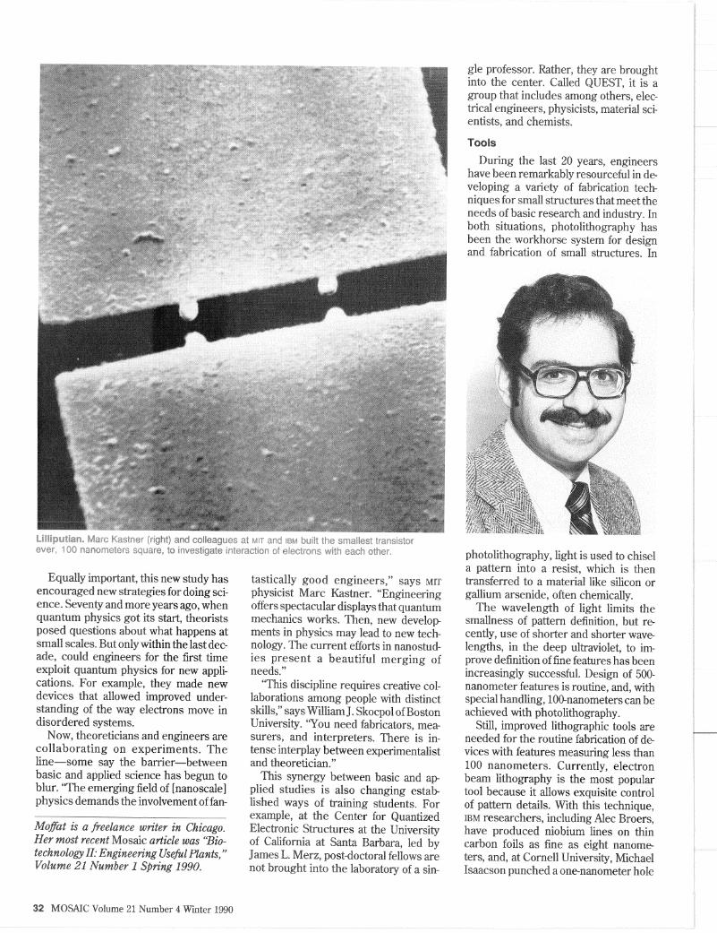
Smith, working with MIT engineer Dimitri Antoniadis and physicist Marc Kastner, is studying extremely small transistors. Recently, Kastner and IBM'S Mordechai Heiblum and Shalom Wind have built the smallest transistor ever, 100 nanometers square. In their device, the conductance oscillates as a function of charge, and each cycle corresponds to the addition of only one electron. This new tool should show how electrons in-teract with each other, and with imperfections in the semiconductor.
'The current experimental strategy is, 'Let's make a novel device and see what happens'," says David Ferry of Arizona State University. *You turn a comer of the road, and you don't know what you are going to find."
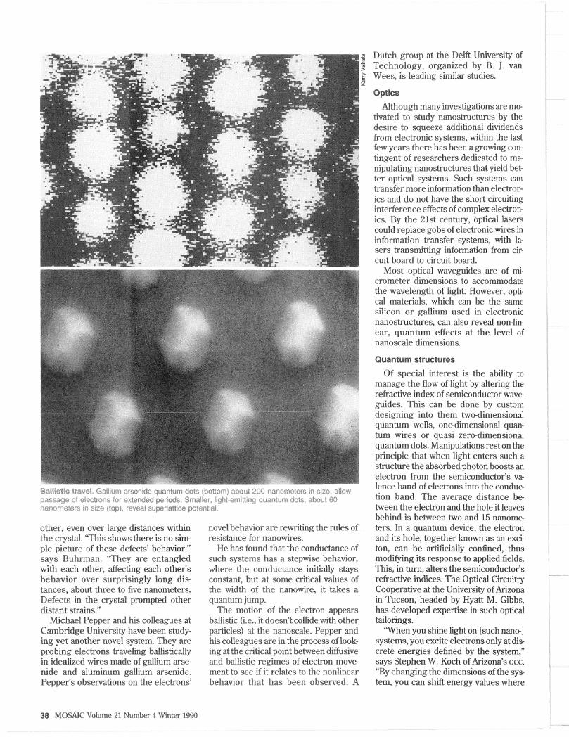
Ferry and his colleagues have used advanced fabrication techniques to produce a complex grid of quantum dots, quasi zero-dimensional specks, with a period of 150 nanometers. This structure revealed a new behavior. The Arizona team noted a strong superlattice potential, a type of double periodicity in conductance, and a weak magnetic effect. However, other teams (at the Max Planck Institute, the University of Munich, and the University of Nottingham) repeated the experiments with similar grids but a weaker potential, and found the inverse.
Ferry says these new phenomena are related to the patterns found in fractals and were predicted by the Russian theorist M. Azbel and Douglas Hofstadter, then of the University of Oregon. "Fractal effects are beginning to be identified in various nanostractures by a number of researchers," says Ferry, stressing that this new type of quantum interfer-
ence remains to be fully explained and controlled.
Damage control
Bob Buhrman's construction at Cornell of totally new nanostructures, known as nanobridges, also resulted in the observation of a novel behavior. His team provided further detail of a phenomenon called electromigration, in which a so-called wind force of electrons, flowing past a defect, eroded the tiny wires, much as water flow can strip a streambank.
This effect is particularly important in small structures, because it contributes to damage in nanowires. It has been known for some time that pure metals are more susceptible to this phenome-non, but the Cornell researchers went one step further: They added impurities to stabilize the defects.
By introducing defects in a gradual fashion, they can tune the wire's trans-port properties so that it has specific conductance fluctuations. The group also found that multiple defects in the tiny nanobridge can interact with one an-
MOSAIC Volume 21 Number 4 Winter 1990 37
other, even over large distances within the crystal "This shows there is no simple picture of these defects' behavior," says Buhrman. "They are entangled with each other, affecting each other's behavior over surprisingly long distances, about three to Ive nanometers. Defects in the crystal prompted other distant strains."
Michael Pepper and his colleagues at Cambridge University have been studying yet another novel system. They are probing electrons traveling ballistically in idealized wires made of gallium arse-eide and aluminum gallium arsenide. Pepper's observations on the electrons'
novel behavior are rewriting the rules of resistance for nanowires.
He has found that the conductance of such systems has a stepwise behavior, where the conductance initially stays constant, but at some critical values of the width of the nanowire, it takes a quantum jump.
The motion of the electron appears ballistic (i.e., it doesn't collide with other particles) at the nanoscale. Pepper and Ms colleagues are in the process of looking at the critical point between diffusive and ballistic regimes of electron movement to see if it relates to the nonlinear behavior that has been observed. A
Dutch group at the Delft University of Technology, organized by B. J. van Wees, is leading similar studies.
Optics
Although many investigations are motivated to study eanostractures by the desire to squeeze additional dividends from electronic systems, within the last few years there has been a growing contingent of researchers dedicated to manipulating nanostractures that yield better optical systems. Such systems can transfer more information than electronics and do not have the short circuiting interference effects of complex electronics. By the 21st century, optical lasers could replace gobs of electronic wires in information transfer systems, with lasers transmitting information from circuit board to circuit board.
Most optical waveguides are of micrometer dimensions to accommodate the wavelength of light. However, optical materials, which can be the same silicon or gallium used in electronic nanostractures, can also reveal non-linear, quantum effects at the level of nanoscale dimensions.
Quantum structures
Of special interest is the ability to manage the flow of light by altering the refractive index of semiconductor wave-guides. This can be done by custom designing into them two-dimensional quantum wells, one-dimensional quantum wires or quasi zero-dimensional quantum dots. Manipulations rest on the principle that when light enters such a structure the absorbed photon boosts an electron from the semiconductor's valence band of electrons into the conduction band. The average distance be-tween the electron and the hole it leaves behind is between two and 15 nanome-ters. In a quantum device, the electron and its hole, together known as an exci-ton, can be artificially confined, thus modifying its response to applied fields. This, in turn, alters the semiconductor's refractive indices. The Optical Circuitry Cooperative at the University of Arizona in Tucson, headed by Hyatt M. Gibbs, has developed expertise in such optical tailorings.
'"When you shine light on [such nano-] systems, you excite electrons only at discrete energies defined by the system," says Stephen W. Koch of Arizona's occ. "By changing the dimensions of the system, you can shift energy values where
38 MOSAIC Volume 21 Number 4 Winter 1990

you want them and thus manipulate optical properties of the nanostructures. Such manipulations, which reduce the dimensionality of the systems, concentrate oscillator strength into particular regimes," he adds, "one step further in the direction of the bandstracture engineering already employed in quantum wells and strained-layer systems."
According to theory, quantum wells yield confinement in one dimension, quantum wires in two, and quantum dots in all three space dimensions. Over the past decade, researchers have achieved much success in constructing quantum wells, but fabricating wires continues to be more elusive, and producing quantum dots still harder.
The possibility of achieving quantum-confined structures has already resulted in quantum-well lasers with threshold currents less than those of bulk hetero-stracture lasers. In principal, quantum-wire and quantum-dot lasers could have even lower thresholds if the inhomoge-neous distribution of materials did not spread out the density of states more than quantum confinement narrows it.
In the early 1980s, long before nano-fabrication etching and molecular beam epitaxy growth techniques were devel
oped, A. I. Ekimov of the Vavilov Optical Institute in Leningrad noticed unexpected peaks in the linear absorption spectra of glasses doped with semiconductors such as cadmium sulfide. Shortly after, the Efros brothers of the Ioffe Physico Technical Institute in Leningrad, explained that these peaks arise from quantum-confinement effects of cadmium sulfide quantum dots that grow in the glass during the heat treatment process used to change the color of the glass. This finding followed on the work done in the late 1950s by the late E. M. Lifshitz and V. V. Slezov, of the Physical Technical Institute in the Ukraine, who analyzed a growth process in which the larger dots grow at the expense of the smaller ones.
Quite similar results have been achieved independently by Lou Bras and coworkers at AT&T Bell Laboratories, using semiconductor crystallites in colloidal systems. Risbud, Khitrova, and Gibbs at Arizona are the first U.S. group, outside of industrial research teams at Schott or Corning, to grow quantum dots in glass. No other technique using solids has yielded quantum dots with clearly defined quantum-confinement peaks. Moreover, Koch's
group at the occ developed the first consistent theory for the nonlinear properties of quantum dots.
Gibbs" group has also fabricated 60 nanometer quantum dots from gallium-arsenide/aluminum-gallium-arsenide quantum wells, using electron-beam lithography (carried out at the Cornell Nanofabrication facility) then reactive ion etching. They also used polystyrene and silicon dioxide spheres as masks to etch cylinders with diameters as small as 40 nanometers. However, no group has detected luminescence from etched dots (that is, lasing quantum dots) with diameters that are less than about 80 nanometers.
Still, within the past year, successful techniques for the growth of optically active nanowires via molecular beam epitaxy, have been announced. Eli Kapon of Bellcore in Red Bank, New Jersey, has produced such wires by growing them on patterned substrates, and the groups of Larry A. Coldren, Pierre Petroff, and James Merz at the University of California at Santa Barbara have announced the fabrication of lasing quantum wires using their titled super-lattice growth techniques.
B. P. VanderGaag and Axel Scherer,
Practical devices
Many of the same advanced fabrication procedures being used to develop the nanoscale structures needed to study quantum physics have also led to practical electronic devices with promise for the near future. Here is a sampling of the first generation of such devices:
• Christopher K Dyer, of Bell Communications Research in Morristown, New Jersey, has developed a miniaturized fuel cell that can be used as a tiny electrical power source for a circuit's microscopic components. It converts chemical energy derived from a reaction between hydrogen and oxygen into electrical energy. The device uses a porous aluminum oxide membrane, 200 to 500 nanome-ters thick, placed between two thin platinum films that act as electrodes. When exposed to air and hydrogen at room temperature, the device develops a potential difference of about one volt between electrodes and yields a few milliwatts of power per square centimeter of membrane area. The details of why it works remain unknown, but Bell researchers are now studying ways to deposit these nanostructures on the integrated circuits.
• At the Naval Research Laboratory in Washington, D.C., Henry Grey has taken a back-to-the-future approach with the development of a tiny vacuum tube whose size is measured in micrometers or smaller. The old-style models, invented about 1907 to function as amplifiers and
switches, were troubled by their large size (centimeters), vulnerability to heat, and low current density. However, the new models, one-hundredth the thickness of a human hair, are immune to the effects of radiation, unlike conventional transistors, because the transport channel is a vacuum and not vulnerable to radiation. Moreover, the remaining problem of low current density is being solved: It is equivalent to that found in standard, but not high-performance transistors.
• Another traditional device to be redesigned on an ultrasmall scale is the diode. Conventional diodes are used in high-speed circuitry to transform alternating current into direct current. They use a phenomenon known as negative differential resistance. As the voltage across a diode increases, induced current decreases. A diode switch is turned on by a low voltage and off by a high one. Late in 1989, Jene Golovchenko and his team at Harvard University and a second group, including In-Whan Lyo and Phaedon Avouris at IBM'S T. J. Watson Research Center in Yorktown Heights, New York, reported the design of an atomic scale diode. They brought the sharp probe of a scanning tunneling microscope close to the surface of a boron-doped crystal When the probe was positioned over isolated defects, a diode effect appeared. That is, the current dropped as the voltage increased. • ASM.
MOSAIC Volume 21 Number 4 Winter 1990 39

also of Bellcore, have produced quantum dots of dimensions under ten nanometers, although it is uncertain whether such structures are optically active. Kerry Vahala of the California Institute of Technology has also produced non-lasing quantum dots and quantum wires. The current challenge, however, is to make lots of such tiny, perfect structures. * What we want to make is whole arrays of structures that are uniform," Vahala says.
Micromechanics
Researchers focusing on the mechanics of the ultrasmall have not yet reached the nanoscale; devices measured in micrometers are the state of the art. But even at these dimensions, physics is often dominated by effects that differ from those of the human-scale world. Richard S. Muller, Roger T. Howe and their colleagues at the University of California at Berkeley have fashioned a number of tiny lamps, resonant structures, and motors during the past two years that are not yet intended for direct application but do prove the feasibility
of select fabrication procedures. Such devices present a special challenge to the fabricator since, unlike nanoelectric devices, micromachines are free-standing, three-dimensional mechanical structures. (Fabricators of nanoscale electronics are sometimes called flat-landers by their colleagues.)
Such small, moving devices also allow researchers to probe their unique qualities, which, at this scale, are shaped more by especially strong frictional forces than by the inertia of the moving parts. Conventional predictive theory fails for objects with this friction relative to mass, and special test structures to probe these effects are being investigated by the Berkeley group under Albert P. Pisano.
Jacob Israelachvili of the University of California at Santa Barbara has taken an important step in explaining nonlinear frictional forces, by gathering data showing that, at the scale of nanometers, such forces are quantized. By studying two mica surfaces pressed together with an organic solvent in between, he found that the thin layer of solvent, acting as
a lubricant of sorts, aligns into a whole number of molecular layers. In this case, frictional forces seem to be quantized according to the number of the monolayers of select organic solvents.
As the pace of basic studies on nano-structures accelerates, there is ongoing debate on how and when these recently discovered phenomena may be harnessed for practical needs, since many of the newly described effects have been revealed using ultraclean rooms and low temperatures and voltages, experimental parameters not useful in the real world. Still, there is little disagreement that understanding of what Webb calls "the bizarre, unexpected phenomena that rear their lovely heads at small dimensions" is essential if science is to propel the next century's technology. •
The National Science Foundation contributes to the support of the research described in this article through several programs in its Divisions of Electrical and Communications Engineering, Chemical and Thermal Systems Engineering, and Materials Research.
40 MOSAIC Volume 21 Number 4 Winter 1990