nanostructured arrays of semiconducting …fulltext.calis.edu.cn/nature/nmat/9/1/nmat2567.pdfstudied...
TRANSCRIPT

ARTICLESPUBLISHED ONLINE: 1 NOVEMBER 2009 | DOI: 10.1038/NMAT2567
Nanostructured arrays of semiconducting octahedralmolecular sieves by pulsed-laser depositionAnais E. Espinal1, Lichun Zhang2, Chun-Hu Chen3, Aimee Morey3, Yuefeng Nie4, Laura Espinal1,Barrett O. Wells4, Raymond Joesten3, Mark Aindow1,2 and Steven L. Suib1,2,3*
Cryptomelane-type manganese oxide (OMS-2) has been widely used to explore the semiconducting and catalytic propertiesof molecular sieves with mixed-valent frameworks. Selective synthesis of patterned thin films of OMS-2 with hierarchicalnanostructures and oriented crystals is challenging owing to difficulties in preserving the mixed valence, porosity andcrystalline phase. Here, we report that pulsed-laser ablation of OMS-2 in an oxygen-rich medium produces a three-dimensionalnanostructured array of parallel and inclined OMS-2 fibres on bare substrates of (001) single-crystal strontium titanate.Both parallel and inclined OMS-2 fibres elongate along the [001]OMS-2 direction. The parallel fibres interact strongly with thesubstrate and grow epitaxially along 〈110〉STO with lattice misfits of less than 4%, whereas the inclined fibres are oriented with(301) parallel to the substrate surface. The spontaneous orientation of the crystalline OMS-2 domains over the STO surfaceopens up a new avenue in lattice-engineered synthesis of multilayer materials.
Porous materials, such as molecular sieves and zeolites, showexceptionally useful properties in catalysis, petroleum re-fining, gas cleansing, separation, membranes and chemical
sensors1–3, owing to their stable frameworks composed of micro,meso and macroporous tunnels that selectively allow access tospecific ions, molecules and clusters. Controlled fabrication ofhighly oriented three-dimensional (3D) films in which functionalcrystal surfaces are more accessible further enhances and op-timizes their already novel functionalities2 as in membranes3,4,photocatalysts5 and sensors5.
Conventional methods for preparing oriented films involvelengthy liquid-phase chemistry approaches or hydrothermal treat-ments that require the use of templates or seeds to directcrystallization3–5. Cancrinite6 and chabazite7 have been reported togrow epitaxially on sodalite using hydrothermal treatment for theformation of the zeolite film. Thin films of other zeolites8–10 andmolecular sieves11,12 have been prepared by combining pulsed-laserdeposition (PLD) for the seeding step with hydrothermal treatmentfor the formation of the film. Amorphous titanium oxide has beengrown in a nanocolumnar array by PLD, but such a structurerequired a polystyrene colloidal monolayer as a template5. Otherprocedures require indirect methods of deposition that involve insitu decomposition of target compounds through laser ablationthat induce deposition of the actual desired material. Thin films ofLa0.5Sr0.5FeO3 fibres perpendicular to strontium titanate (SrTiO3,STO) substrates have been prepared by PLD through decompo-sition of a La0.5Sr0.5FeO3 target13, although both the target andsubstrate materials have the same dense perovskite structure. Thedevelopment of procedures that produce 3D structures of porousmaterials bymeans of self-assembly (seedless) and direct depositionfrom a target of the correspondingmaterial would facilitate scale-upand improve cost-effectiveness.
Cryptomelane-type manganese oxide is the most extensivelystudied of the manganese oxide octahedral molecular sieves(OMS) owing to its excellent catalytic activity and semiconductor
1Institute of Materials Science, University of Connecticut, Storrs, Connecticut 06269-3136, USA, 2Chemical, Materials & Biomolecular Engineering,University of Connecticut, Storrs, Connecticut 06269-3222, USA, 3Chemistry Department, University of Connecticut, Storrs, Connecticut 06269-3060,USA, 4Department of Physics, University of Connecticut, Storrs, Connecticut 06269-3046, USA. *e-mail: [email protected].
properties14. The oxide is designated OMS-2 and has a compositionof KMn4+
7 Mn3+O16, where the charge imbalance on the octahedralframework owing to reduction of Mn4+ to Mn3+ is balancedby K+ in one dimensional tunnels along the c axis. This mixedvalence in the structure is what gives OMS-2 materials their goodsemiconducting properties15. A myriad of synthetic methods andmorphologies have been reported for OMS-2 (ref. 16). Althoughoriented films of OMS-2 would be highly desirable for numerousapplications, preparation of such films has proven to be verychallenging owing to the difficulty in maintaining the mixedvalence, porosity and crystal phase of the cryptomelane structure.
To address the need for the development of highly orientedthin films of OMS-2 with a 3D nanostructured architecture, wehave used a method that involves deposition of OMS-2 ontosingle-crystal (001)STO by means of self-assembly using directlaser ablation of a target made of OMS-2 powder material. STOhas the cubic perovskite structure (a = 0.391 nm) and is anexcellent substrate for the epitaxial growth of high-temperaturesuperconductors andmany other oxide-based thin films17. PLDwasused in this work owing to its ability to produce thin films of awide variety of complex oxides in which the stoichiometry of thetarget is replicated in the film. This technique uses a high-energyultraviolet laser, with laser pulses as short as 10–15 fs, capableof ablating a thin surface layer from a target while leaving theremainder of the target virtually unheated18. The present workshows the direct formation of a nanostructured array of OMS-2with an open architecture of parallel and inclined fibres, whichprovide more surface accessibility both for sensing applications andfor the deposition of other functional materials.
In a typical experiment, a single-crystal (001)STO substrate isplaced in the PLD chamber and heated at a rate of 20 ◦Cmin−1up to 600 ◦C under a vacuum of ∼1 × 10⁻⁶ torr. Then a KrFexcimer laser (wavelength=248 nm, pulselength=20 ns) is used toablate the OMS-2 target material using a partial pressure of oxygenof ∼200mtorr for the desired deposition time. At the end of the
54 NATURE MATERIALS | VOL 9 | JANUARY 2010 | www.nature.com/naturematerials
© 2010 Macmillan Publishers Limited. All rights reserved.

NATURE MATERIALS DOI: 10.1038/NMAT2567 ARTICLES
200 nm
Inclined fibre
500 nm
∠49°
∠90°
Z
YX
Parallelfibres
Inclinedfibres
(001) STO
(001)STO
OMS-2 nanostructure array
a b
c
e
h
f g
d
500 nm 200 nm
200 nm 500 nm200 nm
Figure 1 | Morphology and evolution of the OMS-2 nanostructured array. a–d, Secondary-electron SEM micrographs of the OMS-2 nanostructured arrayprepared by PLD at 600 ◦C using 200 mtorr partial pressure of O2 on a single-crystal (001)STO substrate for 5 min (a,b) and for 30 min (c,d) (top andcross-sectional views in each case). e–g, Secondary-electron SEM images of deposits formed after 30 min showing regions at increasing distance from amask edge giving successively smaller reductions in incident flux as compared with the film deposited without a mask in c,d. h, Schematic illustration of theOMS-2 nanostructured array derived from the secondary-electron SEM images. Within the array, two different fibre arrangements are observed withrespect to the substrate surface: inclined fibres and parallel fibres.
deposition, the partial pressure of oxygen is increased to 300 torrand the film is then allowed to cool slowly at a rate of 2 ◦Cmin−1until room temperature is reached.
The OMS-2 nanostructured arrays grown on (001)STO byPLD were observed using secondary-electron imaging in thescanning electron microscope (SEM). Planar and cross-sectionalviews are shown after different deposition times: 5min (Fig. 1a,b)and 30min (Fig. 1c,d). Figure 1a,b reveals the morphology of thenanostructured array with fibres in two distinct arrangements. Thefirst is composed of orthogonal arrays of fibres that lie with theirmajor axes parallel to the 〈110〉 directions in the STO surface (seeparallel fibres in Fig. 1h), whereas the second is composed of fibresthat are inclined at an angle of approximately 50◦ to the STOsubstrate surface and for which the major axes lie parallel to the〈100〉 directions in the STO surface in projection (see inclinedfibres in Fig. 1h). Figure 1a,b suggests that a deposition time of
5min is not enough to obtain a dense film that would cover thesubstrate completely. Increasing the deposition time to 30mingreatly improves the homogeneity of the nanostructured array (seeFig. 1c,d). Both the morphology and thickness were very uniformacross the substrate surface for the 30-min-deposition samples. Thethickness of this film was ∼200 nm and the length and thicknessof the inclined fibres were approximately 200 nm and 60 nm,respectively. The OMS-2 target material also showed a fibre-likemorphology but with fibre sizes varying from 20 to 60 nm in widthand 200 to 500 nm in length (see Supplementary Section S1).
A further PLD experiment was carried out in which a maskwas used to block the path of the plume to part of the substratesurface. At the edges of the masked regions, the effective materialflux was greatly reduced; as a result, the secondary-electron SEMimages obtained from such regions gave a useful insight into theevolution of the fibre arrangements. Three examples are shown
NATURE MATERIALS | VOL 9 | JANUARY 2010 | www.nature.com/naturematerials 55© 2010 Macmillan Publishers Limited. All rights reserved.

ARTICLES NATURE MATERIALS DOI: 10.1038/NMAT2567
in Fig. 1e–g, which were obtained at increasing distances from theprojected position of the mask edge (that is, increasing materialflux from Fig. 1e–g). These images reveal a gradual development ofthe parallel fibre morphology from the initial nuclei, with averageparticle sizes and length-to-width ratios (L/W ) of approximately28 nm with L/W = 1.2, 42 nm with L/W = 1.3 and 216 nmwith L/W = 1.6, respectively. The images also suggest that theinclined fibres nucleate directly on the STO substrate before thecoalescence of the parallel fibres, although we cannot preclude thepossibility that there is a thin layer of the parallel fibre depositbetween the inclined fibres and the substrate. We assume that thecomposition of the initial nuclei is the same as that of the filmand therefore such films may arise from these nuclei. A schematicrepresentation of the arrangement for these nanostructured OMS-2arrays is shown in Fig. 1h.
The OMS-2 powder target material and a sample of theOMS-2 nanostructured array on the (001)STO substrate werecharacterized by X-ray diffraction (XRD) and representative XRDpatterns are shown in Fig. 2. The 2θ angles and intensities ofthe peaks in the pattern from the OMS-2 target material (Fig. 2,bottom) are in good agreement with the standard pattern for thepure tetragonal cryptomelane phase (JCPDS 29-1020), although aregression analysis of the data revealed that the lattice parameterswere 0.4% larger (a0=0.986 nm and c0=0.286 nm, compared witha0= 0.982 nm and c0= 0.285 nm for the standard). All of the peaksin the correspondingXRDpattern from the thickest nanostructuredfibre array (Fig. 2, top) could also be identified as arising from thecryptomelane phase of MnO2. The regression analysis gave similarvalues for the lattice parameters (a0=0.988 nm and c0=0.286 nm),demonstrating that the structure and stoichiometry of the targetmaterial had been preserved. Themain difference between the XRDpatterns obtained from the nanostructured array and that from thetarget is the absence of certain diffraction peaks. Thus, in Fig. 2, top,all of the hkl peaks for which l 6= 0 are absent, with the exception ofthe 301 peak. This gives clear evidence for strong crystallographictexture in the deposit, although it was not possible to reconcile thesystematic absences with any single orientation relationship withrespect to the substrate.
Cross-sectional transmission electron microscopy (TEM) anal-ysis was carried out to investigate the relationship between theuniquemorphology revealed in the secondary-electron SEM imagesof the OMS-2 nanostructured array and the crystallographic texturesuggested by the XRD pattern. To preserve all of the fibre featuresin the array, the cross-sectional TEM samples were prepared byfocused ion beam (FIB) milling with the section plane parallelto (110)STO (see Supplementary Section S2). A bright-field TEMimage obtained from one such specimen is shown in Fig. 3a. Threetypes of fibre can be identified, as shown schematically in Fig. 3b:(1) parallel fibres A, with their major axes parallel to [11̄0], whichlies in the plane of the TEM cross-section, (2) parallel fibres B, withtheir major axes parallel to [110] (that is, perpendicular to fibresA) and thus appear ‘end-on’ in the image and (3) inclined fibresC, with major axes that lie in the plane of the cross-section but areinclined at an angle of approximately 50◦ with respect to the surfaceof the film. We note that although the fibres have well-definedcharacteristic aspect ratios, their cross-sections are rather irregular(see fibres B in this section).
Electron energy-loss spectroscopy (EELS) mapping with aGatan imaging filter detector was used to reveal the distributionof the chemical species within the section. One example isshown in Fig. 3c, which is a bright-field image together with thecorresponding O–Mn–Ti element map. The map was obtained bymultivariate histogram analyses based on multiple spatially alignedimages of EELS elemental maps for O, Mn and Ti individualelements. Such maps confirm that the OMS-2/STO interface isabrupt and energy-dispersive X-ray spectrometry (EDXS) spectra
(40
0)
OM
S-2
(420
)OM
S-2
(30
1)O
MS-
2
(220
) O
MS-
2
(411
)OM
S-2
(60
0)
OM
S-2
(521
)OM
S-2
(310
) O
MS-
2
(211
) O
MS
-2
(00
2) S
TO
(00
1) S
TO
(1 10
) O
MS-
2
(2 0
0)
OM
S-2
(111
) A
l
(20
0)
Al
Al
Inte
nsity
(a.
u.)
5 10 15 20 25 30 35 40 45 50 55 60 652 (°)θ
Figure 2 | Crystal structure and preferred orientation. XRD patterns ofthe OMS-2 powder target material (bottom) and the OMS-2nanostructured array on single-crystal (001)STO substrate prepared byPLD at 600 ◦C using 200 mtorr of O2 partial pressure for 30 min (top).The indices of reflecting planes belonging to the OMS-2 phase (JCPDS29-1020), STO (JCPDS 35-734) and aluminium (JCPDS 4-787) areindicated. The peaks corresponding to the planes (211), (411) and (521) ofthe OMS-2 phase are missing in the XRD pattern of the nanostructuredarray suggesting that the deposit has a strong crystallographic texture withrespect to the (001)STO substrate.
obtained from the fibres in this region show no evidence ofinterdiffusion of the substrate cations (see Fig. 3d).
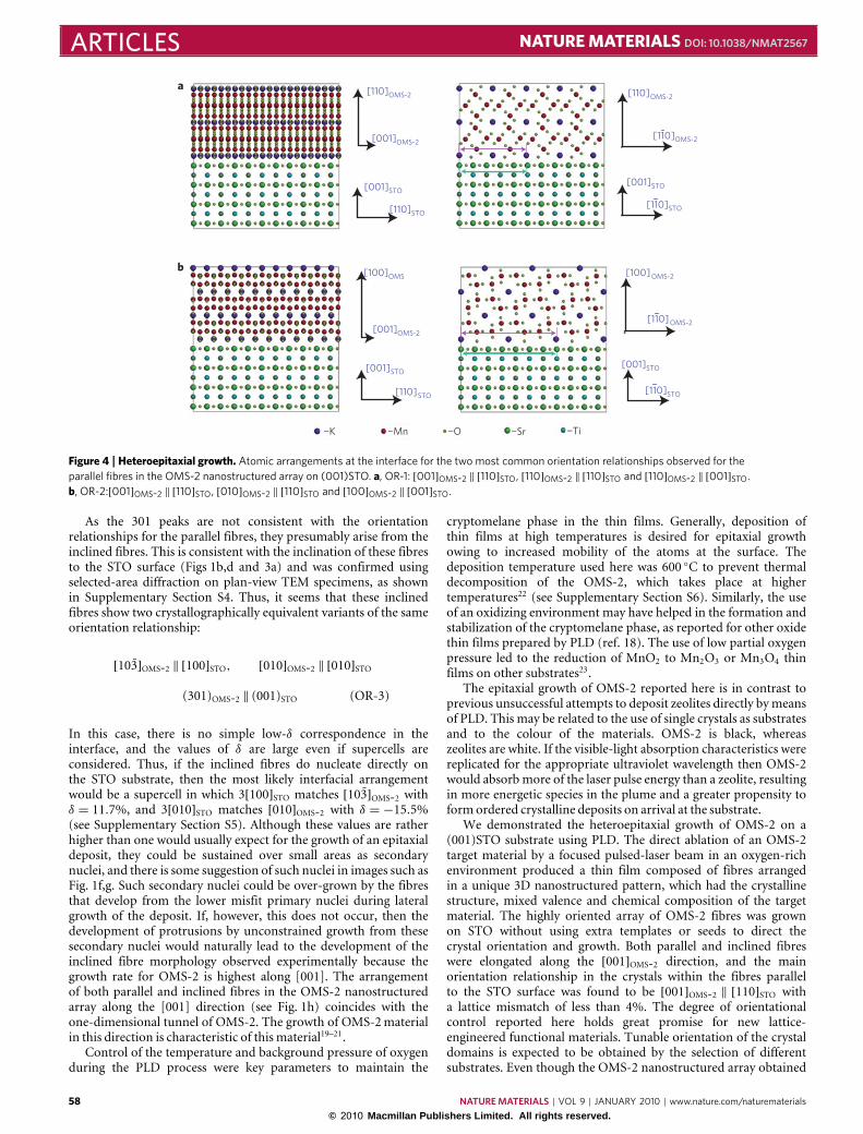
The crystallographic orientation relationship between the OMS-2 fibres and the single-crystal (001)STO substrate was deduced fromhigh-resolution TEM (HRTEM) lattice images. Two examples areshown in Fig. 3e and f, which were obtained from the interface withfibres A1 and B2 in Fig. 3a, respectively. A lattice fringe analysisreveals that these fibres have their major axes parallel to [001]OMS-2,and that they adopt inequivalent orientation relationships withrespect to the (001)STO substrate, with fibre A1 having:
[001]OMS-2 ‖ [11̄0]STO, [110]OMS-2 ‖ [110]STO,
(110)OMS-2 ‖ (001)STO (OR-1)
whereas fibre B2 has:
[001]OMS-2 ‖ [110]STO, [010]OMS-2 ‖ [11̄0]STO,
(100)OMS-2 ‖ (001)STO (OR-2)
From a series of such images it was found that the two sets ofparallel fibres (A and B) show a mixture of different orientationrelationships with (OR-1) and (OR-2) being the most common.All of the other orientation relationships observed also had[001]OMS-2 ‖ 〈110〉STO. We note that this multiplicity of orientationrelationships leads to the formation of grain boundaries betweenadjacent fibres with different orientation relationships, or evenwithin a single fibre (for example, Fig. 3g and h, respectively). It isthought that this latter effect may be related to the rather irregularcross-sections shown by the fibres.
To understand the formation of these multiple orientationrelationships, it is useful to consider the atomic arrangements forthe various interfacial configurations. The [11̄0]STO and [110]STOprojections of the structures on either side of the interface for(OR-1) are shown in Fig. 4a. In the first projection, the misfit, δ,between the primitive lattice translation vectors 0.5[110]STO and
56 NATURE MATERIALS | VOL 9 | JANUARY 2010 | www.nature.com/naturematerials
© 2010 Macmillan Publishers Limited. All rights reserved.

NATURE MATERIALS DOI: 10.1038/NMAT2567 ARTICLES
40 nmSTO
Parallel fibres
Incl
ined
fibr
es
4 nm 4 nm 8 nm
110110
110
110
100
001
110
110
110110
8 nm
110
110
110
100
100 110
110
110
O
Mn
Cu
Pt
K
Mn
Cu
Pt
Pt
B1 B2B3 B4 B5
B6
B7
A1A2
C1C2
C3
C5C4
Pt
STO 200 nm
Parallel fibre A Parallel fibre B Inclined fibre C STO
0 2 4 6 8 10 12 14
a
b
c
e f g h
d
010
110
Figure 3 | Microstructure of the OMS-2 nanostructured array. a, Cross-sectional TEM image of the OMS-2 nanostructured array deposited on a(001)STO substrate by PLD. The TEM specimen was FIB-cut along [110]STO. b, Schematic showing the three groups of fibres (A, B and C) of Fig. 3a.c, TEM image with a corresponding colour-coded O–Mn–Ti elemental map (blue for O, red for Mn and green for Ti) constructed from energy-filtering data.d, EDXS elemental analysis of one inclined fibre. e–h, HRTEM images of the parallel fibre A1/STO interface (e), parallel fibre B2/STO interface (f),boundary between parallel fibres B2/B3 (g) and within fibre B5 (h).
[001]OMS-2 is only 3.4%. No such simple low-δ correspondenceexists in the orthogonal direction, but one can identify a supercellin which 2.5[11̄0]STO matches [11̄0]OMS-2 with δ= 1.1%. Figure 4bcontains the corresponding [11̄0]STO and [110]STO projections ofan A fibre with (OR-2). Here again, δ along the major axis ofthe fibre is 3.4%, but in the orthogonal direction a supercell isrequired to obtain a modest value of δ; in this case, the supercellinvolves 3.5[11̄0]STO matching 2[01̄0]OMS-2, giving δ= 2.1%. Thus,the most likely explanation for the parallel OMS-2 fibres adopting(OR-1) and (OR-2) with respect to the STO substrate is theexistence of low-misfit supercells in the atomic interfacial structureat these orientations. Similar arguments can be applied to the otherorientation relationships observed experimentally, although theseare less common than (OR-1) and (OR-2).
Most of the features in the XRD pattern can be accountedfor on the basis of the orientation relationships adopted bythese parallel fibres. As the X-ray diffractometer samples thoseplanes oriented parallel to the specimen surface, and the com-mon feature of the orientation relationships for the parallel fi-bres is [001]OMS-2 ‖ 〈110〉STO, one would expect all of the hklpeaks for which l 6= 0 to be absent, as observed experimentally(with the exception of 301, which is discussed below). More-over, as the preferred orientation relationships are (OR-1) and(OR-2), one would expect an enhancement in the 110 and 200peaks, respectively, over that for a randomly oriented powdersample (such as the target material); here again, this effect isobserved experimentally in the XRD pattern (Fig. 2, top, andSupplementary Table S1).
NATURE MATERIALS | VOL 9 | JANUARY 2010 | www.nature.com/naturematerials 57© 2010 Macmillan Publishers Limited. All rights reserved.
ARTICLES NATURE MATERIALS DOI: 10.1038/NMAT2567
[110]OMS-2
[110]OMS-2
[110]OMS-2
[110]STO[110]STO
[001]OMS-2
[001]OMS-2
[100]OMS [100] OMS-2
[001]STO[001]STO
[110]STO
[001]STO
[110] OMS-2
[110]STO
[001]STO
¬K ¬Mn ¬O ¬Sr ¬Ti
a
b
Figure 4 | Heteroepitaxial growth. Atomic arrangements at the interface for the two most common orientation relationships observed for theparallel fibres in the OMS-2 nanostructured array on (001)STO. a, OR-1: [001]OMS-2 ‖ [110]STO, [110]OMS-2 ‖ [110]STO and [110]OMS-2 ‖ [001]STO.b, OR-2:[001]OMS-2 ‖ [110]STO, [010]OMS-2 ‖ [110]STO and [100]OMS-2 ‖ [001]STO.
As the 301 peaks are not consistent with the orientationrelationships for the parallel fibres, they presumably arise from theinclined fibres. This is consistent with the inclination of these fibresto the STO surface (Figs 1b,d and 3a) and was confirmed usingselected-area diffraction on plan-view TEM specimens, as shownin Supplementary Section S4. Thus, it seems that these inclinedfibres show two crystallographically equivalent variants of the sameorientation relationship:
[103̄]OMS-2 ‖ [100]STO, [010]OMS-2 ‖ [010]STO
(301)OMS-2 ‖ (001)STO (OR-3)
In this case, there is no simple low-δ correspondence in theinterface, and the values of δ are large even if supercells areconsidered. Thus, if the inclined fibres do nucleate directly onthe STO substrate, then the most likely interfacial arrangementwould be a supercell in which 3[100]STO matches [103̄]OMS-2 withδ = 11.7%, and 3[010]STO matches [010]OMS-2 with δ = −15.5%(see Supplementary Section S5). Although these values are ratherhigher than one would usually expect for the growth of an epitaxialdeposit, they could be sustained over small areas as secondarynuclei, and there is some suggestion of such nuclei in images such asFig. 1f,g. Such secondary nuclei could be over-grown by the fibresthat develop from the lower misfit primary nuclei during lateralgrowth of the deposit. If, however, this does not occur, then thedevelopment of protrusions by unconstrained growth from thesesecondary nuclei would naturally lead to the development of theinclined fibre morphology observed experimentally because thegrowth rate for OMS-2 is highest along [001]. The arrangementof both parallel and inclined fibres in the OMS-2 nanostructuredarray along the [001] direction (see Fig. 1h) coincides with theone-dimensional tunnel of OMS-2. The growth of OMS-2materialin this direction is characteristic of this material19–21.
Control of the temperature and background pressure of oxygenduring the PLD process were key parameters to maintain the
cryptomelane phase in the thin films. Generally, deposition ofthin films at high temperatures is desired for epitaxial growthowing to increased mobility of the atoms at the surface. Thedeposition temperature used here was 600 ◦C to prevent thermaldecomposition of the OMS-2, which takes place at highertemperatures22 (see Supplementary Section S6). Similarly, the useof an oxidizing environment may have helped in the formation andstabilization of the cryptomelane phase, as reported for other oxidethin films prepared by PLD (ref. 18). The use of low partial oxygenpressure led to the reduction of MnO2 to Mn2O3 or Mn3O4 thinfilms on other substrates23.
The epitaxial growth of OMS-2 reported here is in contrast toprevious unsuccessful attempts to deposit zeolites directly bymeansof PLD. This may be related to the use of single crystals as substratesand to the colour of the materials. OMS-2 is black, whereaszeolites are white. If the visible-light absorption characteristics werereplicated for the appropriate ultraviolet wavelength then OMS-2would absorbmore of the laser pulse energy than a zeolite, resultingin more energetic species in the plume and a greater propensity toformordered crystalline deposits on arrival at the substrate.
We demonstrated the heteroepitaxial growth of OMS-2 on a(001)STO substrate using PLD. The direct ablation of an OMS-2target material by a focused pulsed-laser beam in an oxygen-richenvironment produced a thin film composed of fibres arrangedin a unique 3D nanostructured pattern, which had the crystallinestructure, mixed valence and chemical composition of the targetmaterial. The highly oriented array of OMS-2 fibres was grownon STO without using extra templates or seeds to direct thecrystal orientation and growth. Both parallel and inclined fibreswere elongated along the [001]OMS-2 direction, and the mainorientation relationship in the crystals within the fibres parallelto the STO surface was found to be [001]OMS-2 ‖ [110]STO witha lattice mismatch of less than 4%. The degree of orientationalcontrol reported here holds great promise for new lattice-engineered functional materials. Tunable orientation of the crystaldomains is expected to be obtained by the selection of differentsubstrates. Even though the OMS-2 nanostructured array obtained
58 NATURE MATERIALS | VOL 9 | JANUARY 2010 | www.nature.com/naturematerials
© 2010 Macmillan Publishers Limited. All rights reserved.

NATURE MATERIALS DOI: 10.1038/NMAT2567 ARTICLESis not a single crystal, these porous thin films may be veryuseful as substrates for the manufacture of ultrahigh-surface-areacomposites for multifunctional device applications in the field ofcatalysis, energy storage and photovoltaics. This work also suggests apathway towards the formation of similar nanostructureswith othercomplex porous oxides such as zeolites.
MethodsOMS-2 target material preparation. OMS-2 powder material was prepared by asol–gel combustion method22. The procedure involved the preparation of solutionA by mixing 10mmol of potassium nitrate and 4.6mmol of manganese nitratein 50ml of deionized and distilled water. Solution B was prepared by dissolvingglycerol, used as crosslinking agent, in 30ml of deionized and distilled water.The molar ratio of salts to glycerol was set to 1:2. Solution B was slowly added tosolution A while stirring at room temperature until a homogeneous clear solution(solution C) was formed. Evaporation of solution C was carried out on a hot plateuntil the water was completely removed. The recovered dry gel was heated to 250 ◦Cfor 6 h and later calcined at 600 ◦C for 6 h. The yield of this preparation is about 4 gof OMS-2 powder. OMS-2 target material was prepared by pressing about 2 g ofOMS-2 powder into a cylindrical pellet of 2.5 cm×0.3 cm using a mechanical coldpress. The pressure used was about 70MPa and the holding time was 6min, whichassured the pellet was dense enough for the ablation process.
PLD experiments. PLD experiments were carried out using pellets of the OMS-2material as targets and single-crystal (001)STO as substrates (MTI Corporation)with dimensions of 10mm×10mm×0.5mm. Before deposition, the substrateswere cleaned using ethanol in an ultrasonication bath for 20min and handledwith care. Bare substrates of (001)STO were subsequently glued on the heater ofthe PLD system with silver paste to enhance the thermal conductivity during theheating process. The PLD chamber was evacuated to a base vacuum pressure of∼1×10⁻⁶ torr before deposition. The temperature of the substrate was controlledand monitored throughout the processes of heating, deposition and cooling. Thepartial pressure of oxygen during deposition was kept at 200mtorr, using an oxygenflow of 10 sccm; whereas during the cooling period, the oxygen partial pressurewas increased to 300 torr. The conditions of the laser were 22 kV, repetition rate4Hz and 200 J, operating at a fluence of 11 Jmm−2. This laser passed through theultraviolet-grade fused-silica window and into a vacuum chamber with an angle ofincidence of 45◦ relative to the target surface. The distance between the substrate,which was held upside down inside the chamber, and the target was∼9.5 cm. Boththe substrate and the target were rotated (at 10 and 13 r.p.m., respectively) to avoidlocal heating during the laser ablation.
Characterization. The resulting OMS-2 nanostructured arrays were characterizedusing XRD, SEM, TEM, EELS and EDXS. Lattice parameters, average particlesizes and orientation relationships were determined to understand the formationof this unique nanostructured array. XRD measurements were carried out usinga Scintag XDS 2000 diffractometer with a Cu Kα X-ray source using a currentand voltage of 40.0mA and −45.0 kV, respectively. The films were attachedto an aluminium holder and XRD patterns were collected in step-scan modewith a step size of 0.02◦ and a dwell time of 10 s. SEM studies were carried outusing a Zeiss DSM 982 Gemini field-emission scanning electron microscopewith a Schottky emitter operating at 2.0 kV with a beam current of 1.0mA. Thethicknesses of the films were determined by imaging the cross-section of thesamples with field-emission scanning electron microscopy. The average particlesize and the lattice parameters were calculated using the ImageJ24 and Unitcell25programs, respectively. The cross-sectional TEM specimen was prepared witha FEI Strata 400 Dual Beam FIB and later examined with a JEOL 2010 FasTEMoperating at 200 kV. This latter instrument is equipped with a high-resolutionobjective lens pole-piece (spherical aberration coefficient Cs= 0.5mm) givinga point-to-point resolution of <0.19 nm in phase-contrast images. Chemicalmicroanalysis was carried out using an EDAX Phoenix atmospheric thin-windowEDXS. In addition, the elemental maps of the specimen were collected using aGatan imaging filter detector. The image filtering was carried out using the O K-,Mn L- and Ti L-edges at 532, 540 and 456 eV, respectively. The structural modelof interfacial features observed in the HRTEM images was established and analysedusing CrystalKit26 software.
Received 22 July 2009; accepted 6 October 2009;published online 1 November 2009
References1. Corma, A. From microporous to mesoporous molecular sieve materials and
their use in catalysis. Chem. Rev. 97, 2373–2419 (1997).2. Davis, M. E. Ordered porous materials for emerging applications. Nature 417,
813–821 (2002).3. Lai, Z. et al. Microstructural optimization of a zeolite membrane for organic
vapour separation. Science 300, 456–460 (2003).
4. Dong, J., Lin, Y. S., Kanezashi, M. & Tang, Z. Microporous inorganicmembranes for high temperature hydrogen purification. J. Appl. Phys. 104,121301 (2008).
5. Li, Y., Sasaki, T., Shimizu, Y. & Koshizaki, N. Hexagonal-close-packed,hierarchical amorphous TiO2 nanocolumn arrays: Transferability, enhancedphotocatalytic activity, and superamphiphilicity without ultraviolet irradiation.J. Am. Chem. Soc. 130, 14755–14762 (2008).
6. Okubo, T. et al. Heteroepitaxial growth of a zeolite. Angew. Chem. Int. Ed. 40,1069–1071 (2001).
7. Wakihara, T., Yamakita, S., Iezumi, K. & Okubo, T. Heteroepitaxial growthof a zeolite film with a patterned surface-texture. J. Am. Chem. Soc. 125,12388–12389 (2003).
8. Xiong, C., Coutinho, D. & Balkus, K. J. Jr Fabrication of hollowspheres composed of nanosized ZSM-5 crystals via laser ablation.Micropor. Mesopor. Mater. 86, 14–22 (2005).
9. Muñoz, T. Jr & Balkus, K. J. Preparation of oriented zeolite UTD-1 membranesvia pulsed laser ablation. J. Am. Chem. Soc. 121, 139–146 (1999).
10. Pisklak, T. J. & Balkus, K. J. Preparation and characterizationof UTD-12/ZSM-48 thin films via pulsed-laser deposition.Micropor. Mesopor. Mater. 81, 125–134 (2005).
11. Washmon-Kriel, L. & Balkus, K. J. Preparation and characterization of orientedMAPO-39 membranes.Micropor. Mesopor. Mater. 38, 107–121 (2000).
12. Balkus, K. J. Jr & Scott, A. S. Zeolite coatings on three-dimensional objects vialaser ablation. Chem. Mater. 11, 189–191 (1999).
13. Mohaddes-Ardabili, L. et al. Self-assembled single-crystal ferromagnetic ironnanowires formed by decomposition. Nature Mater. 3, 533–538 (2004).
14. Suib, S. L. Porous manganese oxide octahedral molecular sieves and octahedrallayered materials. Acc. Chem. Res. 41, 479–487 (2008).
15. Tian, Z. R. et al. Manganese oxide mesoporous structures: Mixed-valentsemiconducting catalysts. Science 276, 926–930 (1997).
16. Suib, S. L. Structure, porosity, and redox in porousmanganese oxide octahedrallayer and molecular sieve materials. J. Mater. Chem. 18, 1623–1631 (2008).
17. Vrejoiu, I., Alexe, M., Hesse, D. & Goesele, U. Functional perovskites—fromepitaxial films to nanostructured arrays. Adv. Funct. Mater. 18,3892–3906 (2008).
18. Chrisey, D. B. & Hubler, G. K. Pulsed Laser Deposition of Thin Films(Wiley, 1994).
19. Li, W.-N. et al. Hydrothermal synthesis of structure- and shape-controlledmanganese oxide octahedral molecular sieve nanomaterials. Adv. Funct. Mater.16, 1247–1253 (2006).
20. Yuan, J., Li, W.-N., Gomez, S. & Suib, S. L. Shape-controlled synthesis ofmanganese oxide octahedralmolecular sieve three-dimensional nanostructures.J. Am. Chem. Soc. 127, 14184–14185 (2005).
21. Yuan, J. et al. Superwetting nanowire membranes for selective absorption.Nature Nanotech. 3, 332–336 (2008).
22. Liu, J., Makwana, V., Cai, J., Suib, S. L. & Aindow, M. Effects of alkalimetal and ammonium cation templates on nanofibrous cryptomelane-typemanganese oxide octahedral molecular sieves (OMS-2). J. Phys. Chem. B 107,9185–9194 (2003).
23. Isber, S. et al. Study of manganese oxide thin films grown by pulsed laserdeposition. Thin Solid Films 517, 1592–1595 (2009).
24. Abràmoff, M. D., Magalhães, P. J. & Ram, S. J. Image processing with ImageJ.Biophoton. Int. 11, 36–41 (2004).
25. Holland, T. J. B. & Redfern, S. A. T. UNITCELL: A nonlinear least-squaresprogram for cell-parameter refinement implementing regression and deletiondiagnostics. J. Appl. Crystallogr. 30, 84 (1997).
26. Kilaas, R. & O’Keefe, M. A. in Computer Simulation of Electron MicroscopeDiffraction and Images (eds Krakow, E. W. & O’Keefe, M. A.) (TMS, 1989).
AcknowledgementsWe thank the US Department of Energy (DOE), Geosciences and Biosciences Division,Office of Basic Energy Sciences, Office of Science and NSF award number DMR-0907197,for financial support. We would like to thank R. Ristau for preparing cross-sectionsamples on the FIB-TEM and J. Romanow for helping acquiring secondary-electron SEMimages. X. Shen and F. Galasso were very helpful with suggestions and encouragement.
Author contributionsA.E.E., C.-H.C. and S.L.S conceived and designed the experiments. A.E.E., Y.N. andB.O.W. carried out PLD experiments. A.E.E collected crystal structure data and SEMimages and analysed them along with L.E., R.J. and S.L.S. L.Z. and M.A. collected theTEM data and analysed the orientation relationships. A.M. prepared the OMS-2 targetmaterial. A.E.E., L.E, L.Z., M.A. and S.L.S. co-wrote the paper. All authors discussed theresults and commented on the manuscript.
Additional informationThe authors declare no competing financial interests. Supplementary informationaccompanies this paper on www.nature.com/naturematerials. Reprints and permissionsinformation is available online at http://npg.nature.com/reprintsandpermissions.Correspondence and requests for materials should be addressed to S.L.S.
NATURE MATERIALS | VOL 9 | JANUARY 2010 | www.nature.com/naturematerials 59© 2010 Macmillan Publishers Limited. All rights reserved.