nanoseconds for the masses
TRANSCRIPT

Nanoseconds for the Massesby
Eric VanWykB.S. Electrical and Computer Engineering
Franklin W. Olin College of Engineering, 2007
SUBMITTED TO THE DEPARTMENT OF MEDIA ARTS AND SCIENCES IN PARTIALFULFILLMENT OF THE REQUIREMENTS OF THE DEGREE OF
MASTER OF SCIENCE IN MEDIA ARTS AND SCIENCESAT THE
MASSACHUSETTS INSTITUTE OF TECHNOLOGY
JUNE 2017
@2017 Massachusetts Institute of Technology. All rights reserved.
The author hereby grants MIT permission to reproduce and to distribute publicly paperand electronic copies of this thesis document in whole or in part in any medium now
known or hereafter created.
Signature redactedSignature of the Author: _ Sinaurrda te
Department of Media Arts and SciencesMay 24, 2017
Certified By: Signature redactedNeil Gershenfeld
Professor of Media Arts and Sciences
Signature redactedMI T Center for Bits and Atoms
Accepted By:Pattie Maes
Academic HeadProgram in Media Arts and Sciences
MASSAC SET NTITOF TECHNOLOGY
JUL 3 ? i-ii
LIBRARIESARCHNES

Nanoseconds for the Massesby
Eric VanWykSUBMITTED TO THE DEPARTMENT OF MEDIA ARTS AND SCIENCES IN PARTIAL
FULFILLMENT OF THE REQUIREMENTS OF THE DEGREE OF
MASTER OF SCIENCE IN MEDIA ARTS AND SCIENCES
AbstractHigh precision voltage measurement has become a hidden part of our daily lives. Our phones,our wearables, and even our household appliances now include precision measurement capabilitythat rivals what was once only available in laboratory grade test equipment. Converters with 6digits of resolution and nanovolt noise floors cost less than a dollar and fit into our watches.
In contrast, measurement of fast phenomena remains out of our daily reach, as it requiresequipment too expensive and too unwieldy to be found outside the hands of specialists.Commoditization of sub-nanosecond measurement would improve our ability to process theinformation from spectral sensors, which in turn would impact portable medical diagnostics,environmental monitoring, and the healthy maintenance of the infrastructure we rely on.
Here a novel measurement architecture is presented that enables cost effective measurement ofthese sub-nanosecond phenomena, and is easily integrated into existing digital processes. It isbuilt on the same founding premises that the sigma delta architecture uses to dominate low costprecision measurement:
1) Precise measurement with imprecise components2) Digital logic replacements for analog components3) Trade time for accuracy
A prototype unit constructed from existing digital communication components is shown toachieve 11 equivalent bits of resolution at 3GHz of analog bandwidth, with repeatability betterthan 1 millivolt and 3 picoseconds. Timing uncertainty is shown to be better than 1 picosecond.
Several use cases are presented: Differential dielectric spectroscopy, LIDAR, and USB 3SuperSpeed channel sounding.
Thesis Supervisor: Neil GershenfeldTitle: Professor of Media Arts and Sciences
2
Nanoseconds for the Massesby
Eric VanWyk
The following people served as readers for this thesis:
Signature redactedThesis Reader:
z7 ( Shuguang ZhangPrincipal Research Scientist
MIT Center for Bits and Atoms
A
TSignature redactedThesis Reader: _
Fadel AdibAssistant Professor of Media Arts and Sciences
MIT Media Lab
3

Acknowledgements
Neil - Thank you for making me question each and every assumption, twice. Thank you forcontinuously forcing me out of my comfort zone. I've gained so many new perspectives.
Shuguang and Dorrie - Thank you for welcoming me into your ever expanding web of friends.
Fadel - Thank you for your insights and inputs.
Jamie, Joe, Ryan, Tom, and John - You are the best kind of enablers. Thank you for keepingCBA running smoothly.
Yoko, Bonita, Eddy and Roomba - Thank you for keeping CBA running sanely.
Sam, Will, Amanda, Ben, Prashant, Grace, and Nadya - This has been quite the adventure; thankyou for sharing it with me.
Noah, Lisa, Pranam, and Thras - Thank you for teaching me your magic.
Chris, Steve, and Snowflake - Thanks for being the best EE backup team beer can buy.
Mel, Kristen, Ben, and Eric - Thank you for keeping the bubble open for over a decade.
Jonathan - Thank you for the best part of 2016. Welcome!
Jenny, Emily, Mom, and Dad - Thank You.
4

Table of Contents
ABSTRACT................................................................................................................................... 2
ACKNOW LEDGEM ENTS ..................................................................................................... 4
1 INTRODUCTION................................................................................................................. 8
1.1 APPLICATIONS AND NEEDS ............................................................................................ 8
1.1.1 Food Quality and Safety: Dielectric Spectroscopy.................................................. 8
1.1.2 M edical Imaging: Electrical Impedance Tomography ........................................... 9
1.1.3 Power Efficiency: High Frequency Switching........................................................ 9
1.2 EFFECTS OF FREQUENCY ON M EASUREMENT.............................................................. 10
1.2.1 Taking Advantage ofPrior Knowledge................................................................. 10
1.2.2 Sample and Hold Limits to Frequency Range ........................................................ 10
1.3 ENABLING TECHNOLOGIES .......................................................................................... 10
1.3.1 High Precision Digital Frequency Synthesis........................................................ 11
1.3.2 Jitter Reduction and Low Phase Noise Oscillators ............................................... 11
1.3.3 High Bandwidth Comparators............................................................................... 11
1.3.4 High Speed PH Y ................................................................................................... 11
2 SYSTEM DESIGN AND THEORETICAL ANALYSIS................................................ 12
2.1 TIME GENERATION ARCHITECTURE AND ANALYSIS ................................................... 13
2.1.1 Time Dilation from slow Phase Drift...................................................................... 13
2.1.2 Dual Numerically Controlled Oscillators............................................................. 13
2.1.3 Alternative Generation M ethods............................................................................ 15
2.1.4 Effects of Jitter .......................................................................................................... 15
2.2 VERTICAL RECONSTRUCTION AND ANALYSIS................................................................ 17
2 .2 . 1 A rch itectu re ............................................................................................................... 1 7
2.2.2 Relation to sigma delta and delta converters ........................................................ 17
2 .2 .3 R ip p le ........................................................................................................................ 1 95

2.2.4 Signal to N oise .......................................................................................................... 19
2.2.5 Slope Overload and Slew Rate vs Granularity ...................................................... 20
2.2.6 Secondary Filtering and Oversampling.................................................................. 21
2.2.7 Idle Tones and Lim it Cycles.................................................................................... 22
2.3 D IGITIZATION ................................................................................................................ 24
2.3.1 D igital Interface Requirem ents............................................................................. 24
2.3.2 A nalog to D igital Converter Selection.................................................................... 24
3 IMPLEMENTATION AND PERFORMANCE TESTING ........................................ 25
3.1 SAM PLER CONSTRUCTION AND LAYOUT..................................................................... 25
3.].] Sampling Comparator............................................................................................. 26
3.1.2 Secondary Filter...................................................................................................... 28
3.1.3 Frequency Requirem ents ....................................................................................... 28
3.1.4 D igitizer .................................................................................................................... 29
3.2 STIM ULUS G ENERATION ............................................................................................. 29
3.2.1 D igital O utputs...................................................................................................... 29
3.2.2 SRD PIN com b generator ....................................................................................... 30
3.3 PERFORMANCE TESTING ............................................................................................. 32
3.3.1 Repeatability ............................................................................................................. 32
3.3.2 Traditional Jitter M easurem ent............................................................................. 34
3.3.3 N ew Jitter M easurem ent ........................................................................................ 34
3.3.4 RF D evice Characterization ................................................................................. 36
4 A PPLIC A TIO N S ................................................................................................................ 37
4.1 D IELECTRIC SPECTROSCOPY AT H OM E: EpoxY ........................................................... 37
4 .1 .1 R e s u lts ....................................................................................................................... 3 7
4.2 LID A R .......................................................................................................................... 39
6
4.2.1 M ethod and Setup ................................................................................................. 39
4 .2 .2 R e s u lts....................................................................................................................... 4 0
4.3 FUTURE W ORK: U SB SUPERSPEED M ............................................................................ 40
4.3.] Channel Sounding and Training........................................................................... 41
4.3.2 Sounding Configuration......................................................................................... 41
4.3.3 Use as a Stand-Alone Sensor ................................................................................. 43
5 C O N C LU SIO N A N D FUTUR E W O R K .......................................................................... 44
6 TER M S ................................................................................................................................ 45
7 BIBLIO G R A PH Y ............................................................................................................... 46
7

1 IntroductionAnalog to digital converters are inside most digital devices that respond in some way to thephysical world. They give our processors access to sensors and user interfaces, and therebyoccupy a hidden but crucial role in our daily lives. High precision measurement has advanced tothe point that what used to be laboratory grade test equipment is now found inside smart watchesthat automatically tweet about our workouts with nanovolt precision.
However, high speed measurement has not advanced in accessibility in the same way.Accessible fast transient measurement could impact our in-home medical diagnostics, ourunderstanding of the environment, and the healthy maintenance of the infrastructure we rely on.Unfortunately, it is still limited to equipment too expensive and unwieldy to be found outside ofspecialists' hands.
To make these measurements accessible, this thesis presents a novel combination of synchronousequivalent time undersampling and delta oversampling techniques. Two precisely controlledoscillators drift across each other to produce an extremely high equivalent time sample resolutionin excess of 1018 Hz: An Exahertz. In lieu of a standard sampler, a modified delta converteroversamples many millions of these binary sample events to reconstruct the input waveform:1018 Hz worth of events oversample down to 1012 Hz worth of virtual samples, which in turnachieves ~ 10" Hz of equivalent analog bandwidth. The result is the ability to slowly trace outfast, sub-nanosecond transients with higher precision than any individual component in thesystem. The approach is given the name "Exasampling".
Exasampling aims to do for nanoseconds what sigma delta did for nanovolts.
1.1 Applications and NeedsThe Exasampling measurement approach is optimized for low cost, portable, and embeddablemeasurement of sub-nanosecond phenomena. Although any individual sub-nanosecond event ismillions of times faster than human senses are capable of perceiving, in aggregate they direct andinform the macroscopic world.
In general, increased measurement bandwidth and measurement frequency has the followingbenefits:
1) Enhanced separation of independent phenomena by their spectral signature2) Perception of physically smaller effects3) Avoidance of low frequency interference sources
Three specific applications of these principles follow:
1.1.1 Food Quality and Safety: Dielectric SpectroscopyDielectric spectroscopy is a fast, non-destructive method of electrically measuring an object'smaterial properties. Since its invention in 1901, it has been used in laboratories to measureunknown properties, and in industrial settings to classify known materials. However, theequipment costs are still prohibitive for home use.
8

The food industry uses dielectric spectroscopy to detect contaminants and pests. For example,bottles labeled "olive oil" or "cooking oil" sometimes contain cheaper filler materials, such asother oils, pig lard or even "gutter oil" [1]. Recent work combining dielectric methods withmodern data analysis techniques has shown success in detecting these adulterations [2], but themethodology relies on the Agilent (Keysight) N5230A PNA Network Analyzer, a $65k piece ofequipment that weighs 25 kg. The electric signature of rice weevils between one and tengigahertz can be used to detect their contamination of grain [3], and the ripeness of fruits andvegetables can be measured below 1.8 GHz [4]. The equipment used in these two studies is$40k and larger than a microwave oven; these approaches are not yet ready to protect the homeconsumer from gutter oil and rice weevils.
The limiting factor for the deployment of these sensors to the home is the cost and size of sub-nanosecond measurement.
1.1.2 Medical Imaging: Electrical Impedance TomographyThe electrical properties of the human body vary by tissue type, blood perfusion, and fluidcontent. For example, cancerous masses tend to be more conductive than the surrounding tissue,whereas necrotic tissue is less conductive. This correlation has been successfully used toelectrically classify types of skin cancers [5].
Electrical Impedance Tomography (EIT) forms electrical images of the tissue through the use ofarrays of electrodes. Its originally use was to monitor localized lung function and perfusion [6].Multi-frequency EIT, or EIS, is a candidate to replace mammograms in screening for andlocalizing breast cancer [7], and is being evaluated for non-invasive transrectal prostatescreenings [8]. These methods have the potential to give surgeons the ability to detect andlocalize tissue boundaries during the surgery without the delay of sending out a biopsy.
EIS's imaging resolution is a function of the number of electrodes, and its ability to differentiatetissue is limited by its electrical measurement bandwidth and resolution. The next generation ofEIS based surgical and diagnostic tools will require higher bandwidth and channel count.
1.1.3 Power Efficiency: High Frequency SwitchingSwitched Mode Power Supplies (SMPS) efficiently convert and control electrical power byrapidly pulsing power transistors. Timing parameters are critical to the efficiency and safeoperation of SMPS, but the optimal tuning changes with time, temperature, and loadingconditions. They must be chosen conservatively when information is unavailable, sacrificingpotential efficiency. [9] Online measurement and continuous optimization can save power andincrease controlled power density. [10]
Recent developments in GaN power transistors are pushing SMPS switch times sub-nanosecondand switching frequencies above 25MHz [11]. This allows these GaN stages to have greatlyimproved power densities, but at the cost of making it more difficult to collect real-time data ontheir operation. The transients have severe frequency content at 500 MHz, and EMI out past 1GHz [12], and therefore currently require a high end oscilloscope for proper characterization.
9
Integrating the proposed approach into an SMPS system would allow for online self-monitoringof the relevant waveforms. This has the potential to increase system efficiency, decreaseradiated emissions, and increase system longevity.
1.2 Effects of Frequency on MeasurementThe frequency content of a signal has a large impact on the measurement architecture used. Tobreak this down, there are three commonly conflated frequency metrics for samplingmeasurements: the frequency range, the sampling rate, and the information rate. The Nyquist-Shannon sampling theorem states that if the sampling rate is at least twice the frequency range(bandwidth), the signal can be measured regardless of the underlying information content [13].
1.2.1 Taking Advantage of Prior KnowledgeA pure sinewave with a one nanosecond period (1 GHz) would require at least 2 gigasamples persecond to reconstruct with a Nyquist sampler. However, continuing measurements do notprovide novel information if the nature of the signal source is known. Super-Nyquistmeasurement techniques use prior knowledge in order to be able to measure signals withbandwidths above their sample rate's Nyquist limit.
The examples given in Section 1.1 all have transients that are faster than a nanosecond, but theinformation contained in those signals change slowly. Nyquist measurement is an inefficientoption, because it would require a sample rate much higher than the information rate. Thestability of the signals over time provides the prior knowledge necessary for super-Nyquistmeasurement. Of the existing super-Nyquist techniques, Exasampling is most closely related toEquivalent Time sampling, or synchronous undersampling. The stable signal is driven to berepetitive, which provides the prior knowledge necessary to successfully measure frequencycontent above the Nyquist limit.
1.2.2 Sample and Hold Limits to Frequency RangeThe maximum frequency that an architecture can reliably measure is also limited by its front endcircuitry. A common frequency limiting component is the Sample and Hold Amplifier (SHA).It samples an incoming waveform and holds its value in order to provide the converter a stablevoltage to work with. Interleaving many ADC/SHA pairs can increase the sample rate of theaggregate converter, but cannot extend the maximum sample-able frequency. [14] These SHAcarry the performance burden of the entire converter; the system input bandwidth and accuracyare a direct function of the performance of an individual SHA. [15] [16]
The root of the direct correlation is that a SHA does not assume any prior knowledge about theincoming waveform, and is assumed to be able to accurately sample even a random signal.Exasampling relies on a given sample being very similar in value to the sample immediatelybefore it. This assumption allows the system an extra degree of freedom with which to optimizeperformance.
1.3 Enabling TechnologiesExasampling relies on several key enabling technologies from the high speed digitalcommunication industry. The immense market pressures on wired and wireless communication
10

have commoditized frequency synthesis and high frequency digital. These have not only madethis architecture possible, but have also made it very cost effective.
1.3.1 High Precision Digital Frequency SynthesisFrequency synthesis is at the heart of radio communication. Multi-channel radio systems rely ondigital frequency synthesis techniques to create independent communication channels.Improving the resolution of the synthesizer increases the number of channels available, andincreasing the accuracy decreases the amount of bandwidth that is wasted between channels.
These requirements create market pressure from the telecommunications, networking, andphysical interconnect space, and have led to the creation of a new type of synthesizer necessaryfor the proposed system. So-called "rational" synthesizers are capable of frequency precisionbetter than one part in ten billion [17]. This jump allows a synthesizer to compensate foraccuracy with resolution.
Dual synthesizers are further capable of generating closely spaced frequencies that maintain astable phase drift relationship and a digitally stable frequency ratio. This allows for creation ofbeat frequencies tighter than their individual raw accuracy allows, which can be several orders ofmagnitude higher than previous approaches.
1.3.2 Jitter Reduction and Low Phase Noise OscillatorsHigh speed wired communication relies heavily on low jitter, low phase noise clock sources, astiming uncertainty directly contribute to error rate in these systems. Jitter-blockers are devicesthat are able to produce a low jitter clock source using a noisier reference as an input. These cannow easily achieve picosecond jitter floors, with some devices capable of achieving tens offemtoseconds worth of RMS jitter.
1.3.3 High Bandwidth ComparatorsUltra-high speed latched comparators now have several gigahertz of analog input bandwidth, andspecialized comparators now reach as high as 26GHz. These new comparators favorablycompete with track-and-hold amplifiers.
1.3.4 High Speed PHYThe transmitters used in high speed digital physical layer components (PHY) now havesufficiently fast rise and fall times to generate several gigahertz of frequency content. Forexample, a modem LVPECL output can readily achieve a 35 picosecond rise that contains10GHz of frequency content. These PHYs are often integrated into FPGAs and networkcontrollers.
11
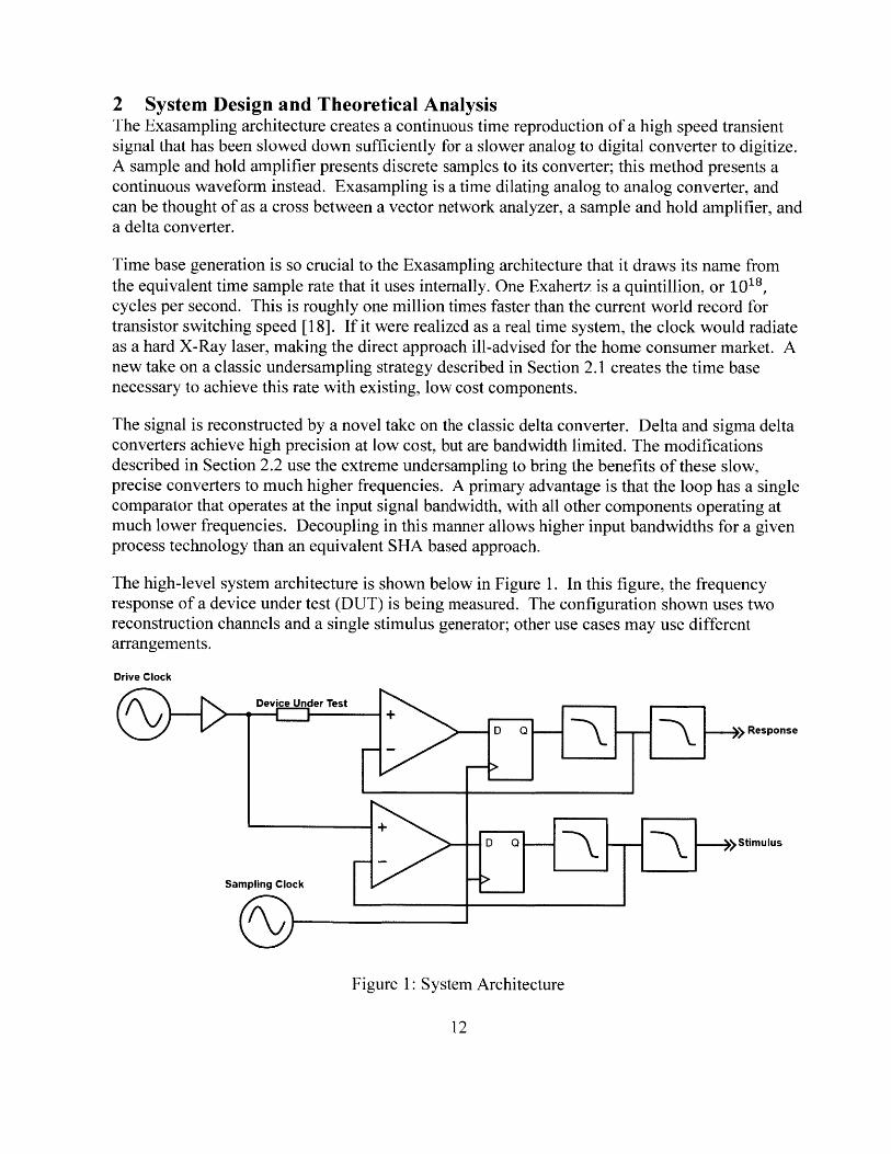
2 System Design and Theoretical AnalysisThe Exasampling architecture creates a continuous time reproduction of a high speed transientsignal that has been slowed down sufficiently for a slower analog to digital converter to digitize.A sample and hold amplifier presents discrete samples to its converter; this method presents acontinuous waveform instead. Exasampling is a time dilating analog to analog converter, andcan be thought of as a cross between a vector network analyzer, a sample and hold amplifier, anda delta converter.
Time base generation is so crucial to the Exasampling architecture that it draws its name fromthe equivalent time sample rate that it uses internally. One Exahertz is a quintillion, or 1018,cycles per second. This is roughly one million times faster than the current world record fortransistor switching speed [18]. If it were realized as a real time system, the clock would radiateas a hard X-Ray laser, making the direct approach ill-advised for the home consumer market. Anew take on a classic undersampling strategy described in Section 2.1 creates the time basenecessary to achieve this rate with existing, low cost components.
The signal is reconstructed by a novel take on the classic delta converter. Delta and sigma deltaconverters achieve high precision at low cost, but are bandwidth limited. The modificationsdescribed in Section 2.2 use the extreme undersampling to bring the benefits of these slow,precise converters to much higher frequencies. A primary advantage is that the loop has a singlecomparator that operates at the input signal bandwidth, with all other components operating atmuch lower frequencies. Decoupling in this manner allows higher input bandwidths for a givenprocess technology than an equivalent SHA based approach.
The high-level system architecture is shown below in Figure 1. In this figure, the frequencyresponse of a device under test (DUT) is being measured. The configuration shown uses tworeconstruction channels and a single stimulus generator; other use cases may use differentarrangements.
Drive Clock
Samp
Device Under Test
D Q - Response
ling Clock
'NJ
D Q >>Stimulus
________________________________I
Figure 1: System Architecture
12
The drive generator produces a repetitive stimulus waveform synchronous to the drive clock(left) from the time base generator. Parameters relevant to the selection of the drive generatorare presented in Section 3.2. The DUT's response waveform enters the sampling comparator'sinput and is reconstructed by the top channel. The stimulus waveform is similarly reconstructedby the bottom channel. The delta reconstructed signal(s) are passed to a secondary low passfilter, and then finally digitized and analyzed as described in Section 2.3.
2.1 Time Generation Architecture and AnalysisThe time base system is responsible for rapidly generating measurement opportunities for thereconstruction system to work with. Whereas a traditional undersampling architecture usesrelatively few but high fidelity measurements, Exasampling uses relatively many measurementswith comparably lower fidelity. The key metrics here are repetition rate and phase offsetconsistency, i.e., many samples that are tightly spaced.
2.1.1 Time Dilation from slow Phase DriftThe sample clock fs and drive clock fD, with periods Ts and TD, are separated by a very smallfrequency offset Af. The two clocks slowly drift across each other with a relative phase drift Aqeach sample period that accumulates to a total phase offset P. As P accumulates, the time basesequentially sweeps through the entirety of the input signal.
A# = Ts - TD
The slow drift produces a time dilation factor, D, which is the ratio of the periods of the originalsignal and its output reconstruction. The value of D is typically on the order of 106 to 1010.
TDTS - TD
As an example, an Exasampling system configured with fs = 100MHz and fD -100MHz+0.lHz produces a relative phase drift Ap ~ 10-17 seconds, or 10 attoseconds. A fullreconstruction cycle takes 0.1 seconds with a dilation factor D = 10'. The reconstructioncollects and uses 10 megasamples during this period.
2.1.2 Dual Numerically Controlled OscillatorsCreating stable, small Af frequency spacing has historically been a difficult task. However, thewireless communication industry relies on well-defined channel spacing for successfulcommunication in the presence of other radios, and has therefore developed several technologiesthat make this now possible.
The key is in using two numerically controlled oscillators that share a single reference time base,and then providing sufficient time for these oscillators to stabilize. A simplified overview isshown in Figure 2.
13

Rational PLL Integer Divider Jitter Blocker
Drive ClockSource Clock
Sample Clock
Figure 2: Frequency synthesis block diagram
A standard crystal oscillator provides a single time base to both synthesizers. Each synthesizer isbased on a "rational" phase locked loop (PLL). These devices provide very high ratiometricprecision, at the expense of added jitter. An integer divider provides some jitter reduction, butmore importantly, it allows the two intermediate frequencies to be dissimilar and well-spaced. Asdiscussed in Section 2.1.4, this decision is intended to reduce crosstalk between the twosynthesizers. Finally, optional jitter blocking PLLs provide the final cleanup to produce theoutput clocks fs and fD.
The input clock is nominally 49.152 MHz. The Drive Rational PLL upconverts this to3.3GHz + 3.3Hz, whereas the Sample Rational PLL upconverts to 3.0GHz nominal. Both ofthese intermediate frequencies are chosen so they are not an integer multiple of the input clock toavoid integer boundary spurs. The Drive Integer Divider downconverts to 1 OOMHz+0. 1Hz, andthe Sample Integer Divider produces 100MHz.
Each step in the clock chain is digital and ratiometric to the input frequency. The time dilationfactor D is therefore "digitally perfect" over a sufficiently long averaging window if there is no"cycle-slip". The combined system accuracy is completely independent of the individualabsolute accuracies.
The absolute accuracy is limited primarily by the accuracy of the original crystal oscillator,which is typically tens of parts per million at birth and drifts strongly with temperature. This isfive orders of magnitude less accurate than what would be required of an independent synthesisapproach. Error in the shared oscillator produces error in the drive frequency, but does notproduce error in the reconstruction of the resulting signal. This can be calibrated out byadjusting TD and Ts, limited by the accuracy of the host's own time base.
14

The oscillators are intended to run uninterrupted for many seconds at a time at any givenfrequency. This allows the jitter blocker filters to be quite aggressive, sacrificing settling timefor further jitter reduction.
The combination of dual rational synthesis, low phase noise oscillators, and long runningstability provides the Af and jitter combination necessary for Exasampling.
2.1.3 Alternative Generation MethodsUndersampling time base generation can be broadly categorized as either controlling the samplephase directly (Sequential or Coherent Equivalent Time), or by sampling at an uncontrolledphase and measuring where it happened to occur (Random or Interleaved Equivalent Time [19]).The time-to-digital or digital-to-time converter determines the maximum equivalent time samplerate and contributes to the sample jitter of the device.
The most closely related method is the Vernier method of time interval measurement, which isoften found in systems with random sample phases. The Vernier method measures a timeinterval by using a pair of startable oscillators with differing periods and a coincidence detector.In 1993 this method achieved sub-picosecond resolution with 2.5 ps jitter. [20]. More generallythis method's resolution is determined by the beat frequency of the two oscillators, and itsaccuracy is determined by the jitter of the coincidence detector and the oscillator start behavior.
A key difference is that whereas Vernier measurement relies on startable oscillators, theoscillators in Exasampling run continuously. This allows the PLLs to be tuned primarily forstability rather than for the start transient, which allows for better jitter performance. Secondly,the absence of a coincidence detector removes its impact on system performance. Lastly, theVernier method uses many clock periods to measure a single time interval, whereas the proposedmethod generates a time interval every single clock period. This removes the inherent lineartradeoff between sample rate and timing resolution, allowing for both a faster real time samplerate and a higher time dilation ratio.
Dual slope or Time Stretching methods are able to achieve a time resolution of roughly 10picoseconds [21]. The resolution of this approach is directly scaled by the time stretch ratio,hence these methods were rejected due to their low repetition rate.
Traveling Wave or Tapped Delay Line [22] methods rely on large numbers of repeated digitalelements. These approaches were rejected due to being unable to obtain suitably low delayelements to achieve the necessary resolution. However, this may be an appropriate solution foran ASIC based approach.
Delay Locked Loops (DLL) are sometimes used in interleaving ADCs to generate phase offsetsbetween their separate track-and-hold channels, and can keep jitter below 600fs [23]. ADCsusing this approach may calibrate out DLL with an aperture adjustment.
2.1.4 Effects of JitterJitter is the all-encompassing term for short term variability in the time base generation system.These fluctuations in the relative timing between the clocks limit the effective system analog
15

bandwidth and distort the reconstructed signal. The effects of random jitter J and phasedependent jitter J(#) modify the ideal steady state response to Y (X(4# + J + J(4))).
Random jitter is the probability distribution of Aq around its nominal value given as J = f(A4);the cycle to cycle variations in exactly when the sample is taken. It is by definition the portion ofthe jitter that is independent of both phase and signal content, and can therefore be independentlyanalyzed. The steady state response becomes Y~(X(4+J)).
Y ~ (X( + M)
N
N2JX(#P +jn)n=1
Expanded by definition
Y f X(p +J)P(J)dj
Which is by definition equivalent to
Y (X * P)(q5)
Writing it in this convolutional sum format allows us to treat the random jitter's probabilitydistribution as the equivalent of an FIR filter applied to the input waveform.
Truly random jitter is typically assumed to be Gaussian in nature and measured in femtosecondsRMS. The effects of random jitter on an Exasampler can therefore be estimated as a Gaussianlow pass filter with a corner frequency given by f, = 1/2wca , where a is the RMS value of thetotal system jitter.
The effect of jitter is typically given as a signal to noise SNR limit equal to -20 log(2fin). Ithas been previously shown that oversampling can exceed this limitation in bandpass receivers.[24]. The reduction in the effect of aperture jitter on an Exasampling system is roughlyequivalent to the reduction shown by Patel et al. taken to an extreme case.
Phase dependent deterministic jitter produces Y = (X(P + J())). This can be viewed as anonlinear mapping between real time and equivalent time, thereby causing distortions as P"wobbles". Oscillator "Lock-In" or "Injection Locking" is the tendency for an oscillator to shiftits frequency or phase to synchronize to another oscillator of similar frequency, and is a likelysource of phase dependent jitter. Assuming that synchronization of the two oscillators did occur,digital error would accumulate and eventually break synchronization temporarily. The oscillatorwould over-correct until the digital error was compensated for and then synchronization wouldoccur again. The system would then continue to alternate between these states, producingdeterministic jitter and spurs.
16

2.2 Vertical Reconstruction and AnalysisVertical reconstruction of the signal is based on an extreme version of oversampling, which inturn relies on having an equivalent time sample rate many times faster than the input signalbandwidth. P sweeps through the input signal slowly enough that many of the analyses canassume it to be stationary.
2.2.1 Architecture
D 0 ADC-
V.
Figure 3: Reconstruction Block Diagram
The block diagram of the reconstruction architecture is shown in Figure 3. The input signal, X,is synchronous to the drive clock f. It is attached to the positive input of the samplingcomparator. The reconstructed signal, Y, is attached to the negative input. The comparator's d-flip-flop samples X(cp) > Y(t) synchronous to the sample clock fs. This serial stream hasvalues V+ and V_, and is filtered to generate Y.
A low speed analog to digital converter digitizes the time dilated and reconstructed signal forfurther processing. This ADC has a Nyquist pre-filter to further eliminate noise from the sampleclock. The digital stream is then filtered and/or demodulated as necessary.
2.2.2 Relation to sigma delta and delta convertersThe core feedback loop and oversampling method is similar to that of the seldom used deltaconverter, which is related to the extremely popular sigma-delta converter [25]. This family ofconverters can achieve high resolutions, but by nature are limited to input bandwidths muchsmaller than would be implied by the Nyquist limit of their internal sample rate.
The delta converter is an analog to digital converter invented in 1946 and then "reinvented" in1952, primarily for the purpose of encoding voice signals. [26] It produces a high rate binarystream representing either a positive or negative delta in the signal's value. Reconstruction isachieved with a simple integrator.
17

-V
Figure 4: Delta Converter Architecture
The sigma delta converter is very similar to the delta converter, differing primarily in theplacement of the integrator. It has greatly improved low frequency accuracy and noiseperformance, and it is currently the dominant architecture for high precision conversion. Thisapproach was patented in 1954 first as an analog to digital encoder, and then expanded on byseveral contributors in the 1960s. [27] [25].
f+D Q - )
+V
-V
Figure 5: Sigma Delta Converter Architecture, 1" order
The Exasampling architecture's cost advantage comes in part from having as few high frequencycomponents as possible; only the sampling comparator is required to handle the full inputbandwidth. This necessitates moving the integrator from the sigma delta position to the deltaposition, meaning that it cannot perform noise shaping in the same way a sigma delta can.
The feedback filter in an Exasampler is not as constrained as it is in a delta converter, because itdoes not have to match a separate reconstruction filter in a receiver. This eliminates the impactof the low frequency drift error common to the delta architecture. Additionally, this feedbackfilter does not even need to be linear, it only has to be stable. This becomes important in thephysically realized system discussed in Section 3.
18

2.2.3 RippleEach sample period increases or decreases the current estimate by AY+. Unlike a purelyintegrating delta converter, this is not symmetric and is dependent on the current value of Y.Given a first order feedback filter with a corner frequency of fF, AY+ is:
AY+ = 2w(V+ - Y)fF fs
AY_ = 27(V_ - Y)fF fs
AY+ = AY+ - AY_ = 2w(V+ - V-)fF/fs
In the ideal case, Y would never deviate by more than 1 x AY+. This assumes that thecomparator always makes the correct decision, and pushes the output back towards the correctvalue.
Comparator hysteresis adds directly to this peak to peak ripple, as it creates a region ofuncertainty around the target value. Samples that fall within the hysteresis window will registerpositive or negative with unpredicted behavior.
Pure delay through the feedback loop can also be a significant contributor to ripple. Withfs = 100 MHz, there is only 10 ns of timing budget for the result of the sampling comparator topropagate through the comparator, the digital hold element, and the output D/A. The outputalone is a significant contributor because there is a trade-off between I and propagation delay,with modern CMOS outputs achieving delays and slew times on the order of 3-6ns. [28]
To first order, the total pure delay through this path forces the comparator to work withinformation from some number of cycles N in the past. Worst case, this linearly increases thepeak output ripple by NAY. This value remains relatively flat with respect to fs above a criticalvalue, as N is proportional, and AY is inversely proportional, to fs. Increased sample speedsdecrease ripple up to a limit dictated by the propagation delay through the loop filter.
AYpp ~ Hys + NAY+
2.2.4 Signal to NoiseThe impact of the AYpp ripple on system performance can be quantified in its Signal to NoiseRatio (SNR). The following calculations assume flat frequency and probability distributions inthe ripple noise. This is a conservative assumption for the probability distribution, and anoptimistic assumption for the frequency distribution, as discussed in Section 2.2.7.
The peak SNR (PSNR) can be measured using either peak to peak noise or RMS noise, a choicethat is primarily driven by the marketing department of the company selling the device. Thecalculations here use peak to peak, resulting in the "flicker free" equivalent resolution. UsingRMS noise for PSNR gives results typically 2.7 bits better than peak to peak.
= noisePSNR = 20 log (fullscale input)
19

PSNR = 20 log(AP )(V+ - V-)
AYpp N2w(V+ - V-)fF/fs + hys
PSNR 20 log 27TNfF/fs + iy)
A filter frequency to sampling frequency ratio of 10,000 gives a limit of -64dB PSNR. Thisimplies any single sample has roughly 11 equivalent bits (ENOB) before oversampling.
2.2.5 Slope Overload and Slew Rate vs GranularityDelta converters must balance their resolution (granularity) and the maximum input slew ratethey can correctly digitize. The condition of an input waveform slewing too quickly for the deltaconverter is referred to as slope overload. An increased step size increases the maximum slew,but also increases the granularity. Some delta converters address this by dynamically adjustingtheir step size. [29]
A similar effect is present in Exasampling. A rapid change in the input waveform may beincorrectly reconstructed if it is too fast for the feedback filter at the current dilation factor.
The slew rate is the continuous time form of the loop filter response, and is given as:
dY-= AYfs = 2 7fF(Y - V+)dt
This can be applied to the input waveform X with the dilation factor as:
i5; D27fF(X - V+)
The slope overload condition can be detected by monitoring the sampling comparators output fora long stream of Os or Is. If necessary, D can be increased, in turn increasing the maximum slewrate at the cost of also increasing measurement time. This provides better control over thebandwidth vs resolution trade off than a traditional delta converter.
The effect is shown in Figure 6. In this simulation, an overload condition occurs at 0.5ps wherethe ideal reconstruction has an instantaneous step change. The output of the samplingcomparator, V(Q) remains high for 11 Ons until the reconstruction output finally slews up to theideal value.
20

V(out) V(Q)15 V(input)on
--- -- -- --- - ----- - --- --
--------------------------
- - - -- -- - - -- -- -II I 110 R III NIII: 11 00 1 lul lIII UU
I I I I i I I0.lps 0.2ps 0.3ps 0.411. 0.5ps 0.6ps 0.7ps
.8I I0.BijS 0.9ps I .Ops
Figure 6: Simulated slope overload - fD = 500 MHz, D = 10A4, f, = 1.6 MHz
2.2.6 Secondary Filtering and OversamplingThe secondary filter decouples the AY+ in the feedback path from the ripple seen by the endconverter. This decoupling provides several benefits including lessened hysteresis effects andshorter idle tone sequences. Additionally, keeping the primary filter first order avoids theconditional stability issues associated with higher order sigma delta and delta converters.
The AYpp ripple noise is spread over a huge bandwidth compared to the reconstructed signal ofinterest. For example, a 10GHz signal reconstructed with D = 109 and fs = 100 MHz has 7decades difference between fy and fs.
The upper limit for SNR improvement from oversampling is given as the ratio of fs/fy. For theexample above, this is nearly 12 effective bits of improvement. However, this assumes aperfectly flat frequency spectrum of the noise, a brickwall oversample filter, and does nothing toimprove the linearity of the system. This is a very optimistic upper bound.
The secondary filter directly affects the measured Y waveform. Passband distortion here can bereflected to the input waveform time domain as DfF2 . Since D can vary with use case, it isrecommended to set the corner frequency of the secondary filter sufficiently high such that at thelowest expected value of D, DfF 2 >> BW.
Filter agility is then achieved in the digital domain. The secondary filter effectively becomes aNyquist filter for the analog to digital converter.
21
720mV-
640mV-i - -
560mV-
48OmV-
400mV-
320mV-
240mV-
160mV-
BOmV-
0.Ops
- -- W- -O O -P -VIVW 0l Pt 9
-- -- - - - -- - - - - - - - - - - - --- ---- - - -
------- ----- -- - - - -- - -------- - - - - - -
-------------- ---------- --- ----
r" -
V(Out) V(Q)/5
----------- ----------
V(input)

2.2.7 Idle Tones and Limit CyclesLimit Cycling is the condition in which a modulator produces a repetitive output bit stream witha fixed output length. Idle tones are a semi-related but less well understood behavior that causessimilar distortions, but does so with bit stream outputs that are not perfectly repetitive. [30].
Both of these effects result in distortion at subharmonics of the internal sample rate. Thequantization noise is no longer spectrally flat, and forms peaks. This increases the requirementsof the secondary filter beyond what was calculated in 2.2.3 above. A simulated exaggerated idletone spectrum is shown in Figure 7. A peak 40dB above the noise floor is found at 15.625 MHzwith fs = 500 MHz. This is the 3 2 "d subharmonic.
V(out)
-20dB-
-40dB-
-60B-
-M0B-
-100dB-
-120dB-
-14OdB-
-160dB-
-180dB-
-200dB-
- - - ---------- ------------------ -----------_-- ------ ------- -- ----
k~e ~one0O~ al pea
- ----------------- ----------------- ------- -----
... ~ -. -
- --------
- - ---- -- ------------------ -- - -- - - --
----- ----------
---- -- -- - - - - - - - --- ------+------- - - - --
1MHz 10MHz 100MHz
Figure 7: Idle tone spectrum
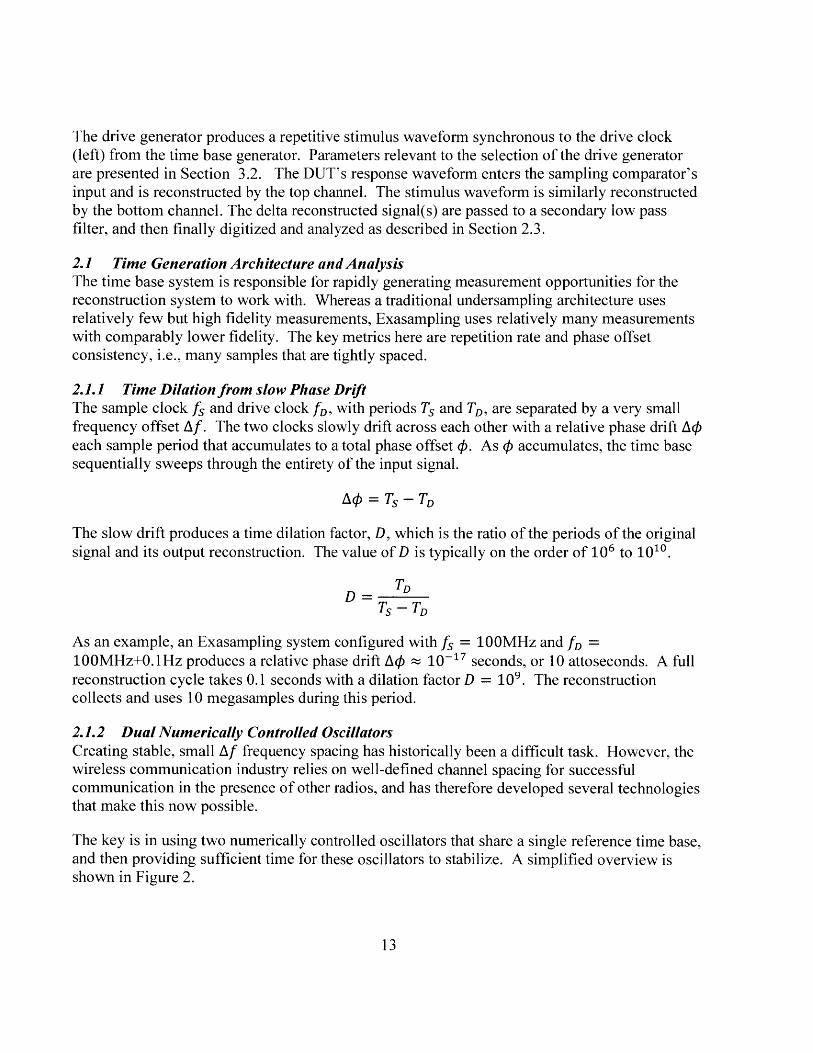
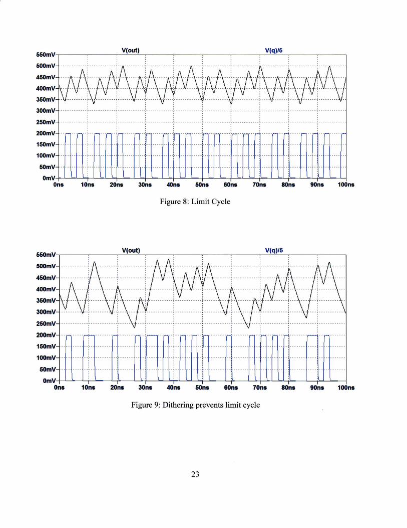
An Exasampler produces similar artifacts dependent on the input value. Figure 8 shows asimulated and exaggerated limit cycle behavior. The output stream repeats the 12 bit sequence"... 101001010100..." for a fixed input of 40% of full range. Adding noise to the input breaksthe limit cycle at the cost of increasing peak to peak ripple, as shown in Figure 9.
22
Do
45
34
30
2
20
Mv-IOM V --------------------------- --- --------- --------------------- ----- ------------ ------------ ------------ ----- -------
---------- ----- ----- -----------
M V -1- --------- ----- ----- ------ - ---- ------------ ----------- - --- ---- --- -r - --- --- ---- - -- -- ---- -- --- ---- --
M V - ------------ ------------ 4------------ ------------- ------------ ------------ ------------ ------------ ------------ -------------
----------- I ------------- ------------- 11 ------------ 11 ------------ 11 ------------- I ------------ 11 -------------6MV - ------------ ------------
MV - -- -- ----- - -- ----- -- ----- -- -- ----- ( - -- ----- - -----
------------ -- ---- ------- -- - ------- ------- ----------I
-- ---- ---- -- ---- -- - -- ------- ------- ------------ ------- ---- -- ---- ------- -- --------- ------- ----------
M v -
- ---- ----
-- ---- -- ----
------- -------
------- ----
- -----
8MV-.
- ---- -- ---- -- --------------- ----- ----0MV-i
L
V( Y5
V(Out) V(qY5
On* Gone 6orm 70no som 90nalong 2Orw 30ris 40rw loorm
Figure 8: Limit Cycle
V(Out)
- --------- ----------- ----------------- --------- ------------ ------------ ------------ ---- ------GMV-. ---- --4MV ------------------ -------- - --- -----
------------ -- --- ---- ---- -- -- L -- -------- I ------------- ------- J-
----- ----- ---------- - - - - - - - - - - - - ------- --------- ---8MV ----- ------ - - - -- - - - - - - - - - -
8M V -- - ---- -- -------- --- - -- ------ ----------- I ------------- ------- ---- r - ------- - --- ------ ---- ---- -- T
-------- -- --- --- --- ------------ ------------ -------- --- ---- --- ------------------- - --- -----------IOMV - ---------
------------ ----- - ---- ------
QM V - ------------- I ------------ ------ - --------------------- ------ -------------------------
-- ----- ------- ------ -- -- -- ------- L ------- -- -- -- ------- -- -------
--- --------- -- --------- ------------ --------- ---- ------------
IOMV-
IOM V - ---- ---- -- r --------- -- --------- - ------- ---- T ------------ --------- -- --------- ---------------------- ---- ------------
-------
----
. ........---- ---- -- I -------4MV
-- ------ --
------- - --------OMV I L:
20rw 30ra 40naon* lorm Gorm Gorm 7orm Sorn
Figure 9: Dithering prevents limit cycle
23
90M loom

2.3 DigitizationThe Exasampling system is an analog to analog converter, and therefore requires an analog todigital converter to bring the signal into the processor. As discussed above, the resultant signalcan carry 10 to 16 bits of useful equivalent resolution, and the resultant bandwidth can bearbitrarily low to fit the system requirements.
2.3.1 Digital Interface RequirementsOne of the hidden costs of direct high frequency measurement is the rate at which data isgenerated and processed. Direct digitization of gigahertz signals generates gigabytes of data persecond, which creates a hard coupling between the bandwidth of the signal and the cost of theassociated digital logic. In contrast, Exasampling and traditional undersampling decouple theanalog and digital bandwidths by their dilation factor. Again, the only component in the entiretyof the Exasampling architecture that carries the full bandwidth requirement is the input to thecomparator; all other components operate at slower, cheaper frequencies.
For reference, consider the processing requirements of sampling a 700 MHz signal at 8 bits and3GS/s, creating a data deluge of 3 gigabytes per second. The ADC083000 from TexasInstruments achieves real time transmission of this using a total of 66 digital logic outputsarranged as 33 differential pairs, each of which must be routed with controlled impedance,terminated, and length matched. This typically requires an FPGA to process. The ADC08B3000is a sister part that uses a piece of high speed memory to buffer up to 4,0000 samples and thenslowly dole them out over a much slower 20 pin 200 MB/s interface. This still requires thedigital logic inside the converter to be operating at 3 GB/s, but is now slow enough for a highend microcontroller.
An equivalent Exasampling system can push the same bandwidth and resolution over a single pinwith an arbitrarily slow data rate, such that an arbitrarily low cost microcontroller can be used.For example, the MSP430FR21 11 from Texas Instruments sells for $0.45 each is sufficient forprocessing a 10 GHz signal at 12 bits of resolution when D = 109. Increasing the performanceof the microcontroller allows the Exasampler to reduce its dilation factor and increase theeffective data rate; the analog and digital bandwidth decoupling allows for a smooth tradeoffbetween cost and quality.
2.3.2 Analog to Digital Converter SelectionThe choice of analog to digital converter can be largely driven by the bandwidth and resolution.The major noise sources in the system are very high frequency compared to the reconstructedsignal; ripple from the delta converter, power supply noise from the stimulus generator, andblow-through from the signal(s) being reconstructed. Active filters may run out of gainbandwidth at these frequencies.
Rather than filtering these sources out, it is possible to use analog to digital converterarchitectures that are inherently less susceptible to them. Architectures with wide aperturesand/or slow settling times are preferred over tighter sampling windows. This odd anti-requirement is similar to that found in coulomb counters. For example, the input integrators indual-slope and sigma delta converters make them preferable to a successive approximationconverter with a sample and hold.
24
-~ 1
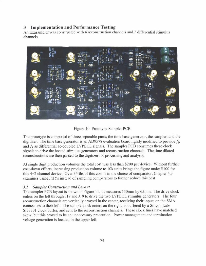
3 Implementation and Performance TestingAn Exasampler was constructed with 4 reconstruction channels and 2 differential stimuluschannels.
Figure 10: Prototype Sampler PCB
The prototype is composed of three separable parts: the time base generator, the sampler, and thedigitizer. The time base generator is an AD9578 evaluation board lightly modified to provide fD
and fs as differential ac-coupled LVPECL signals. The sampler PCB consumes these clocksignals to drive the hosted stimulus generators and reconstruction channels. The time dilatedreconstructions are then passed to the digitizer for processing and analysis.
At single digit production volumes the total cost was less than $200 per device. Without furthercost-down efforts, increasing production volume to 10k units brings the figure under $100 forthis 4+2 channel device. Over 3/4ths of this cost is in the choice of comparator; Chapter 4.3examines using PHYs instead of sampling comparators to further reduce this cost.
3.1 Sampler Construction and LayoutThe sampler PCB layout is shown in Figure 11. It measures 130mm by 65mm. The drive clockenters on the left through J 18 and J 19 to drive the two LVPECL stimulus generators. The fourreconstruction channels are vertically arrayed in the center, receiving their inputs on the SMAconnectors to their left. The sample clock enters on the right, is buffered by a Silicon LabsSi53301 clock buffer, and sent to the reconstruction channels. These clock lines have matchedskew, but this proved to be an unnecessary precaution. Power management and terminationvoltage generation is located in the upper left.
25

Figure 11: Sampler layout
Figure 12: Exasampling unit cell layout
3.1.1 Sampling ComparatorThe sampling comparator is constructed from three independent ICs. Most importantly, theADCMP573 from Analog Devices is a SiGe based high speed sampling comparator with 8 GHzof analog bandwidth. [31]. It is the only component in the system that directly interacts at thefull bandwidth.
Unfortunately, commercially available sampling comparators with comparable bandwidth aretypically latching and use a low swing output stage, such as LVDS, LVPECL, or CML.Exasampling requires a registered output and a full swing output. An On-SemiMC1 OOEP52DTG d flip-flop registers the latched output, and an Analog DevicesADCMP600BKSZ expands the output range to fully cover the input range.
26

UIAADCMP573BCPZ VTT VTT
CLK P 7 R1 R2
CLK N 6'- VTT VTT. ' MCIO0EP52DTG 3V3
Feedback 3 10 U2 3V3 30 R31
1--D VCC kn U62PT 2 + I I D ADCMP600BKSZ Feedback
Q LNUT
S742792095 R324 -Q742792095 2 iw _ __CLK P CLK Ferrite
CLK VEE 1F
GND GND
Figure 13: Sampling comparator and primary filter schematic
This introduces several propagation delays through the feedback loop, as shown in Figure 14.Setup and Hold time of the flip flop is achieved by clocking it on the opposite edge of the latch,and routing the clock line to provide 45 picoseconds of clock skew. The physical impact of thisskew requirement can be seen in the physical separation between Ul * and U2* in Figure 12.
fS Id-
Comparator Output Result1 Resut2
FlipFlop Input / Result ResuIt2
FlpFlop Output
D/A Output
ResuRl s Resu ut2
/ Resufl Result2
Figure 14: Feedback loop timing diagram
The performance penalty of having to translate from latched LVPECL to registered CMOS isroughly 5 nanoseconds plus half a sample period. An equivalent monolithic samplingcomparator would increase resolution by roughly one equivalent bit per the calculations inChapter 2.2.
The primary filter was initially set with fc = MHz. Additional filtering was provided by the21r
slew of the output DAC, and by a series ferrite bead with a notch frequency equal to fD =100 MHz. The total frequency response of this system is shown in Figure 15. The additionalnotching is intended to cut high harmonics out before they have a chance to rectify against thesecondary filter's ESD protection diodes, though system evaluation later showed this protectionto be an unnecessary precaution.
27

Vfls.ord1r) .~rieUu-
410dB-
-20dB
-30-d
40dB-
-dB
-70dB-
-80dB-
-dB-
-100dB-
- d11dB-1i 10Hz 100Hz 1KHz 10KHz 100KHz 1MHz 101Hz 100MHz 1GHz
Figure 15: Primary filter with and without ferrite bead
3.1.2 Secondary FilterThe secondary filter is footprinted as a 4t order low-pass with double corners at 100 kHz and 1MHz, as shown in Figure 16. In retrospect, this approach was overkill, as the additional filteringprovided here did not significantly improve system noise performance.
3V3
1 1OP 2
U3 +Ri 2.67k R2 9.53k
- GNDGND
3V3
U7A 7AD8656ARMZU7
C3 11 OWF 6 AD8656ARMZ7
5-R3 R47.R4 28.7k + OUTPUT
C45
1pF
=- GNDGND
Figure 16: Secondary filter schematic
3.1.3 Frequency RequirementsFigure 17 highlights the relative frequencies of the signals running through the unit cell. Theonly signal that carries the full bandwidth of the input signal is X, shown in green between theinput SMA connector and the comparator. Blue signals operate at fs (nominally 100 MHz); thisis only the clock and the communication lines of the d flip flop. The signals shown in yellow arethe portion of the signal path that operate at the slow, time dilated reconstruction with only a fewkilohertz of bandwidth.
28
-- - - -.- II- T + - - ---- - 'r r T-- -~ w a - . -. A.-.1 -:111 T +r - - - I - . +- - e-- . -4 -+ >9 4s.----c-- - I- - a*:---- : -T T r- -- -n .- ---re> --4-- : a++a
2- 1 17 M. . .. .i . . .. .. .i . I .. .. .1 . 2 ()Iiii l i i IiIII i I iiIII I I 1 7 :1 11 1 . .. .. . I
- -- - - - L - .AJ J L:- - - - . - L .LV A . . .... 1 -... - - . - .c .. 1 -L I LX ..- - - . J . --. I L1J L - ...- J . . .L J J J J L'-.. ...- L .. J -L j6 L'L J ...' .' .L .-i a ...r'- '.- .. AI A A 1
L I l 1 V- L j k. L L Q I - - - - - - - i ii i r i 3 e i i i e i i t i i i0 i g g | | | I g i i g a a i i i i i i e i i 4 i ig g i g a g i ig T 1 * .
-1 - - r - r is T I I T r: -it - - r - 11 -s 1 - r Ir Ir 1s -. - - - - Ti - I: 11 -117 ri - - - T - -rs Ir T T IrN - - r -1 , I sI r- 1 rI rI:,-"Tar .I --' I Ti Ii ~ ~~~~~~~~~~~~~ . . . . . . .t . . . e t s s . . . . - - -0 - -! - - t r i e ieia1 i e eli t i e i i iIi
I i i i i Ii ii i i I i i i iti i e i i a e i a I i* I i i e iis i i i ts 1 i i i i ei t i i i a 1 1 1 1 mi i
z
INPUT
iinsioideis: Vpferrite) 2Cr
- 00
-- 2r
- -600
- -800-~1000
--120r
-41400
-41600
- -1800
. hla. tf
.,%F

To Digitizer
y0
Comparator
X r D FF
fs- LPF 2"d LPF
Figure 17: Unit cell frequencies. Green is 10GHz. Blue is 100MHz. Yellow is 10kHz.
The high frequency section is extremely small and localized; it may be possible to use a coplanarwaveguide layout for X instead of a microstrip in order to remove the need to control thedielectric stack-up. In higher precision applications it may be prudent to place a ferrite chokealong the Y feedback path to further reduce high frequency coupling.
3.1.4 DigitizerDigitization of the reconstructed signal is performed by a Cypress PSoC 5LP programmablesystem on chip. This integrates programmable analog filters, a 48 ksps 16 bit LA ADC, digitalfilter logic, an ARM M3 Cortex operating at 80 MIPs, and a USB 2.0 device port. [32] The fourchannels were filtered, digitized, and passed via the USB port to a MATLAB program for furtherprocessing. Filters optimized in MATLAB can be ported back to the PSoC.
3.2 Stimulus GenerationThe Exasampling system architecture provides a deal of flexibility in what waveform is sent tothe device under test. The only mandatory requirements are that the drive stimulus waveformmust be synchronous to the drive clock and stable over many repetitions. The choice of stimulusgenerator is therefore dependent on the specifics of the device under test and the intendedmeasurement.
Several measurement modes use the drive clock directly without an intervening stimulusgenerator. Other use-cases have the equivalent circuits built into the device-under-test.
3.2.1 Digital OutputsHigh speed digital communications use output buffers that produce a square stimulus waveformwith sharp, well defined edges and have well known output impedances. For example, LVPECLis 500 and can achieve a >35ps rise time. For a well matched DUT, this is essentially a stepresponse measurement. Pairing them with a sampling comparator built on the same standardoften implies that they have matching input and output voltage ranges, and that their analogbandwidths are comparable.
One important note is that many output stages are strongly dependent on their load. Forexample, ECL uses a differential current steered output stage. If one of the outputs is allowed to
29
float, then the current source will overload and collapse when that output is enabled. At the nextclock edge the current source will take time to recover, compromising the turn on transient.
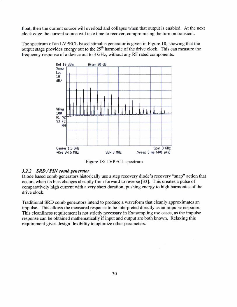
The spectrum of an LVPECL based stimulus generator is given in Figure 18, showing that theoutput stage provides energy out to the 2 5 th harmonic of the drive clock. This can measure thefrequency response of a device out to 3 GHz, without any RF rated components.
Ref 10 dBm$ampLUV
dB/
VAvg100W1 SS3 F
A
Center 1.5 GHzeRes BW 5 MHz
Atten 20 dB
VBW 3 MHzSpan 3 GHz
Sweep 5 ms (401 pts)
Figure 18: LVPECL spectrum
3.2.2 SRD IPIN comb generatorDiode based comb generators historically use a step recovery diode's recovery "snap" action thatoccurs when its bias changes abruptly from forward to reverse [33]. This creates a pulse ofcomparatively high current with a very short duration, pushing energy to high harmonics of thedrive clock.
Traditional SRD comb generators intend to produce a waveform that cleanly approximates animpulse. This allows the measured response to be interpreted directly as an impulse response.This cleanliness requirement is not strictly necessary in Exasampling use cases, as the impulseresponse can be obtained mathematically if input and output are both known. Relaxing thisrequirement gives design flexibility to optimize other parameters.
30
2
A

+12V
MAR3
#1e~
Figure 19: PIN Comb Generator simplified schematic
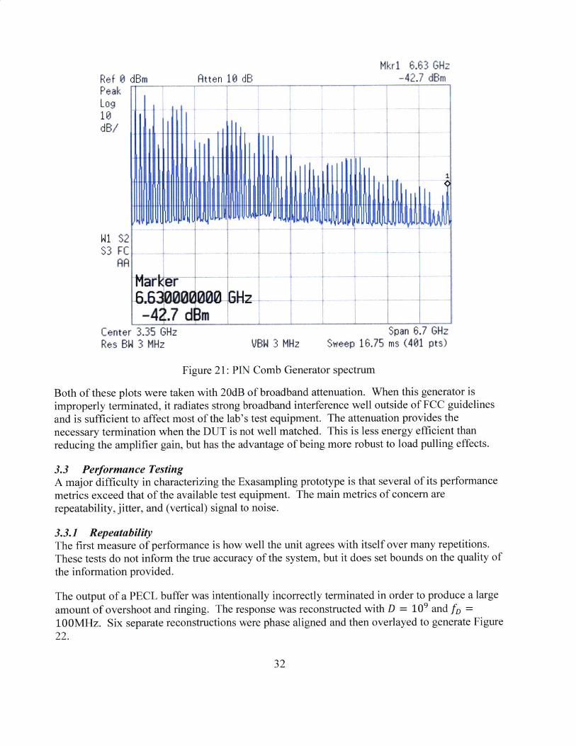
A comb generator was adapted from David Bowman's (GOMRF) Source2 [34] to function as astimulus generator. As shown in Figure 19, the drive clock feeds a MAR3+ wide-band RFamplifier, which then drives in to a HSMP-3822 dual PIN diode. The snap action of this diodepair produces the waveform shown in Figure 20, and the spectral response shown in Figure 21.Note that this was tuned not for a clean impulse, but rather for strong high frequency content.This created harmonic content out to the limits of the spectrum analyzer; -42.7dBc at 6.63 GHz.
This entire subsystem costs less than $2 USD in 1000 piece quantities.
"4-4t I j
jVjel
A, A _IWh
tvv~
Figure 20: PIN Comb Generator waveform
31
-7.A - -MUMVWV_
P71
Ref 0 dBmPeakLog10dB/
Atten 10 dB
F -I U '*I*III liii -I-A--I-I-.a--L-I..5-5-L5-i44-I-I--I4~-#l--
I~iI I I ~iiIiH+IPIUIIIIIII M Mlllfh in H0 I NI I-f
-M0.7 d
Center 3.35 GHzRes BW 3 MHz
3m
VBW 3 MHz
Mkr1 6.63 GHz-42.7 dBm
aSpan 6.7 GHz
Sweep 16.75 ms (401 pts)
Figure 21: PIN Comb Generator spectrum
Both of these plots were taken with 20dB of broadband attenuation. When this generator isimproperly terminated, it radiates strong broadband interference well outside of FCC guidelinesand is sufficient to affect most of the lab's test equipment. The attenuation provides thenecessary termination when the DUT is not well matched. This is less energy efficient thanreducing the amplifier gain, but has the advantage of being more robust to load pulling effects.
3.3 Performance TestingA major difficulty in characterizing the Exasampling prototype is that several of its performancemetrics exceed that of the available test equipment. The main metrics of concern arerepeatability, jitter, and (vertical) signal to noise.
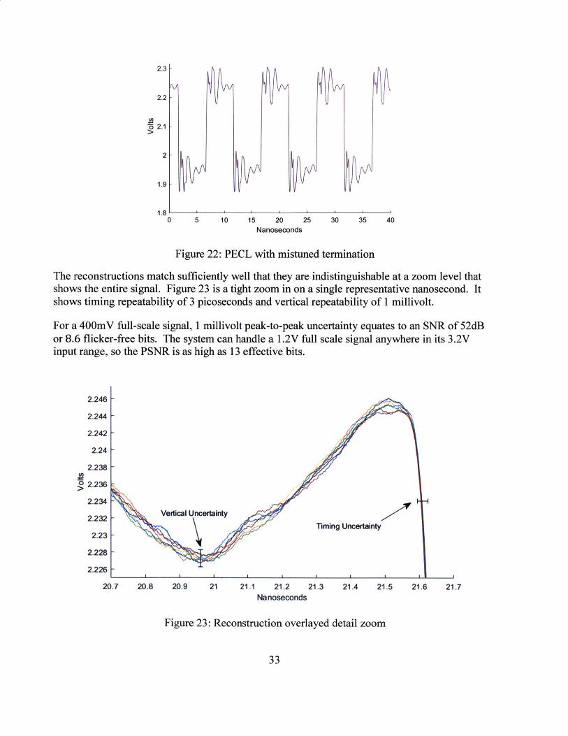
3.3.1 RepeatabilityThe first measure of performance is how well the unit agrees with itself over many repetitions.These tests do not inform the true accuracy of the system, but it does set bounds on the quality ofthe information provided.
The output of a PECL buffer was intentionally incorrectly terminated in order to produce a large
amount of overshoot and ringing. The response was reconstructed with D = 109 and fD =
100MHz. Six separate reconstructions were phase aligned and then overlayed to generate Figure22.
32
W1S3
$2FCAA
-- L-L-ML-JL-L-L i
a
I
%WW W
2.3
2.2
S2.1
2
1.9
1.80 5 10 15 20 25 30 35 40
Nanoseconds
Figure 22: PECL with mistuned termination
The reconstructions match sufficiently well that they are indistinguishable at a zoom level thatshows the entire signal. Figure 23 is a tight zoom in on a single representative nanosecond. Itshows timing repeatability of 3 picoseconds and vertical repeatability of 1 millivolt.
For a 400mV full-scale signal, 1 millivolt peak-to-peak uncertainty equates to an SNR of 52dBor 8.6 flicker-free bits. The system can handle a 1.2V full scale signal anywhere in its 3.2Vinput range, so the PSNR is as high as 13 effective bits.
2.246 -
2.244 -
2.242 -
2.24 -
2.238 -
62.236-
2.234 -
2.234 Vertical Uncertainty
Timing Uncertainty2.23 -
2.228
2.226
20.7 20.8 20.9 21 21.1 21.2 21.3 21.4 21.5 21.6 21.7Nanoseconds
Figure 23: Reconstruction overlayed detail zoom
33
3.3.2 Traditional Jitter MeasurementThe first attempt to measure total system jitter was made with a 7300A Teledyne LecroyOscilloscope. The drive and sample clocks were fed directly into the oscilloscope, which thenmeasured and trended the edge to edge timing. The measured jitter with this method matchedthe Oscilloscope's own channel to channel jitter spec of 2.5ps RMS, and similarly matched itssingle channel jitter spec of 1.0ps RMS. This strongly implies that the Exasampling system'stime base generator is at least matching the performance of the oscilloscope, but it does not allowus to confidently put a number on that performance.
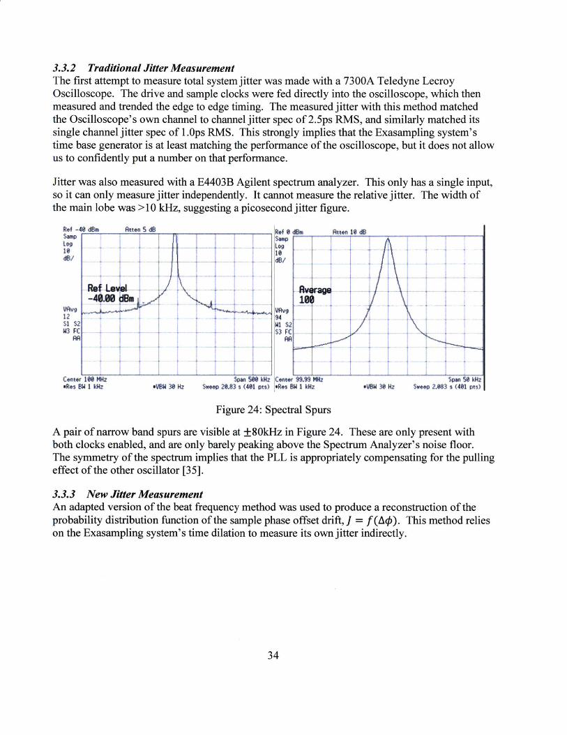
Jitter was also measured with a E4403B Agilent spectrum analyzer. This only has a single input,so it can only measure jitter independently. It cannot measure the relative jitter. The width ofthe main lobe was >10 kHz, suggesting a picosecond jitter figure.
C- e -4 0 - k f k& CW _ _ R tun 1n 5 kdB_
.o ..... Lsm
$1 S2 __ $
Catr 10 MHz -Sma So kcIz Conw 9&19 ftz $wa 50 kHzR9es N lI z VN 30 Nz Sweep 2.83 s (4l pts) eRBs 1 I&z @8N 30 Rz Sweep 2.83 s (401 pts)
Figure 24: Spectral Spurs
A pair of narrow band spurs are visible at +80kHz in Figure 24. These are only present withboth clocks enabled, and are only barely peaking above the Spectrum Analyzer's noise floor.The symmetry of the spectrum implies that the PLL is appropriately compensating for the pullingeffect of the other oscillator [35].
3.3.3 New Jitter MeasurementAn adapted version of the beat frequency method was used to produce a reconstruction of theprobability distribution function of the sample phase offset drift, J = f(A/). This method relieson the Exasampling system's time dilation to measure its own jitter indirectly.
34

Drive Clock
REF
mpling Clock
0-D Q % Jitter
I -.
Figure 25: Configuration for Jitter Self-Test
In this self-test mode, the main feedback loop is broken open-loop and configured as shown inFigure 25. The sampling comparator latches high if the drive clock arrives before the sampleclock. This captures the cumulative total system jitter effects from the drive clock, sample clock,and the comparator. Each sample period is a single test of f(A4) < q, and the averaging fromthe lowpass filter produces a running estimate of the cumulative distribution function F(Ab).The entirety of this distribution is sampled as q5 drifts from negative to positive.
Note that the effects of the low pass filter are irrecoverably included in this measure andsubsequently interpreted as additional system jitter. This is not an issue when measuring totalsystem performance, because this effect is also present during reconstruction. However, it doesmake this a conservative measure when attempting to characterize jitter alone.
Raw results are shown in Figure 26. Time base is 500 microseconds per division with D = 109 ,giving an equivalent time base of 500 femtoseconds per division. The cumulative probabilitydistributions on the rising and falling edges are both shown. Analog persistence captures thedistribution of these measured distributions; horizontal alignment is largely a function of theoscilloscope's trigger.
-2.0 -1.5 -1 .0 -0.5 0 0.5 1.0 1.5 2.0
Figure 26: Jitter probability as a function of nominal phase offset in picoseconds
This data shows a Gaussian distribution of jitter 732 femtoseconds RMS, which aligns well withthe calculated jitter budget and has an equivalent filter corner at fc = 1/2wro- ~ 200 GHz. Thisis well above the filter imposed by the comparator's input bandwidth, and is therefore assumedto be good enough to be ignored in further calculation.
35
100%
00/
-1
Sa
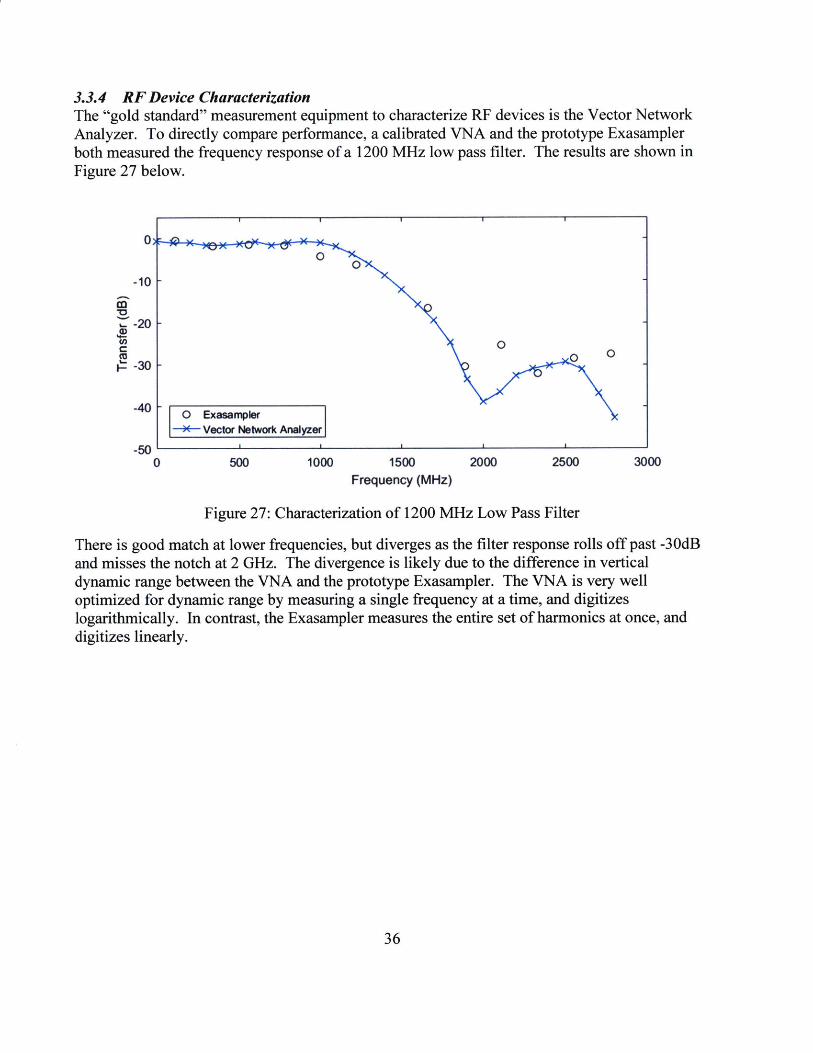
3.3.4 RF Device CharacterizationThe "gold standard" measurement equipment to characterize RF devices is the Vector NetworkAnalyzer. To directly compare performance, a calibrated VNA and the prototype Exasamplerboth measured the frequency response of a 1200 MHz low pass filter. The results are shown inFigure 27 below.
0*-10 -
CO~-20- 0 0
' 30 --
-4 - 0 Exasampler
-+- Vector Network Analyzer
-500 500 1000 1500 2000 2500 3000
Frequency (MHz)
Figure 27: Characterization of 1200 MHz Low Pass Filter
There is good match at lower frequencies, but diverges as the filter response rolls off past -30dBand misses the notch at 2 GHz. The divergence is likely due to the difference in verticaldynamic range between the VNA and the prototype Exasampler. The VNA is very welloptimized for dynamic range by measuring a single frequency at a time, and digitizeslogarithmically. In contrast, the Exasampler measures the entire set of harmonics at once, anddigitizes linearly.
36
4 ApplicationsExasampling excels in applications where the system under test is relatively stable; the rate ofinformation generated is much slower than the frequency of the signal. Three exampleapplications are given.
Dielectric Spectroscopy highlights the Exasampling's ability to look into the chemical propertiesand changes of household materials. LIDAR not only shows the raw temporal resolution of thesystem, but also that good measurement can compensate for bad sensors.
Finally, the improvement to the USB 3 SuperSpeed protocol shown in Section 4.3 shows howthese techniques can be integrated into existing technologies. If the proposed improvement isadopted by the USB IF, then as a side-effect all future USB 3 devices and hosts would be able tomake Exasampled measurements natively.
4.1 Dielectric Spectroscopy at Home: EpoxyDielectric spectroscopy provides a non-invasive, non-destructive method of evaluating thecomposition and state of a sample. The cost per test is very cheap, as it usually does not requireany consumable or disposable components. However, the upfront cost is prohibitive for thehome market. [36]
Exasampling makes spectral sensing affordable for the home, consumer, and personal healthmarkets. This accessibility can bring better understanding and more fulfilling interactions withthe chemical processes that affect our daily lives. Potential applications include refrigerators thatcan detect milk souring before a human nose can, pill bottles that ensure the efficacy of theircontents, and cars self-diagnose lubricant degredation. [37]
Dielectric monitoring of epoxy curing is a Double/Bubble@ Red Extra Fast Setting EpoxyAdhesive is a two part epoxy with an advertised work time of 3 to 5 minutes. The Exasamplingsystem was used to monitor this chemical reaction in real time.
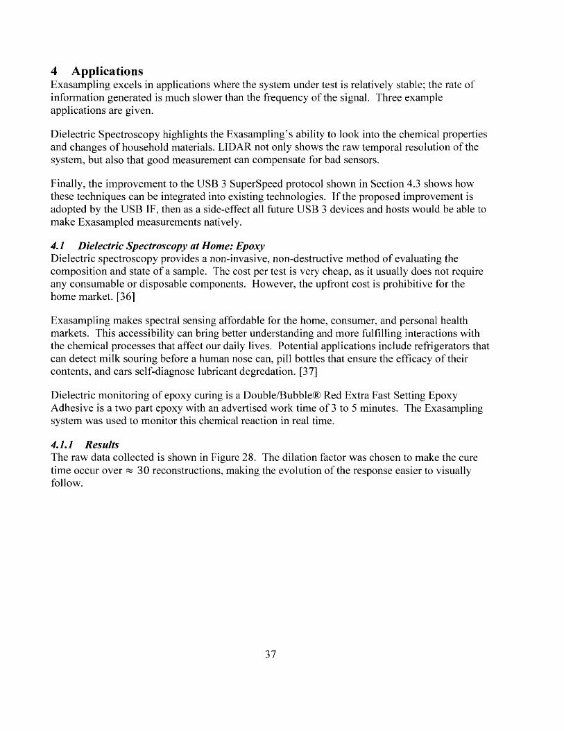
4.1.1 ResultsThe raw data collected is shown in Figure 28. The dilation factor was chosen to make the curetime occur over ~ 30 reconstructions, making the evolution of the response easier to visuallyfollow.
37
0.5
0 50 100 150Time (seconds)
200 250
0
300
Figure 28: Epoxy Cure Test
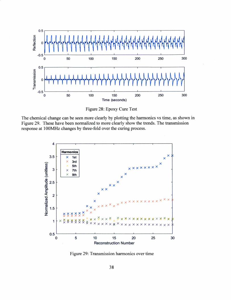
The chemical change can be seen more clearly by plotting the harmonics vs time, as shown inFigure 29. These have been normalized to more clearly show the trends. The transmissionresponse at 100MHz changes by three-fold over the curing process.
HarmonicsX 1stx 3rd
5th- X 7th
X 9th
x xx- XX
5
x
X x
x
X
x xX X
xxXxxx x
xx
XxxxxxxxX
XX
X~XXXX)*xx~XX:XxXxXXxxxxxx;:
10 15 20Reconstruction Number
25
Figure 29: Transmission harmonics over time
38
C0
C.0
0 50 100 150 200 250 30
0
-0.5
0.5
0
-0.5
4
3.5
I-
)3
2.5
2
1.50
1
0.50 30
X *
X~~ ~ X x X x X X X X X XXX XXt

4.2 LIDARTime-of-flight imaging uses the time delay between the light source and receiver to measuredistance, examine sub-surface phenomena, and even see around corners. [38] This sectiondescribes measurement of sub-millimeter changes in the path length of a light beam usingExasampling and an optical Ethernet PHY. Although not a full LIDAR, this test case highlightsboth the temporal resolution improvement that Exasampling provides to time-of-flight systems,and its ability to measure phenomena with greater fidelity than the underlying sensor nativelysupports.
4.2.1 Method and SetupFixed Electrical Delay
Drive Clock D Q Reference
+ D 0Variable Optical Delay Delay
PHY TXJ R
Sampling Clock
Figure 30: Exasampled LIDAR Architecture
The time-of-flight measurement is performed using a two channel Exasampler, as shown inFigure 30. The primary channel measures a variable delay optical path with an optical EthernetPHY and produces result Y1. The second channel directly converts the drive clock through afixed delay line to produce result Y2.
Cheap Optical Ethernet PHYs are easy to electrically interface with an Exasampling system.The Broadcon AFBR5972 and AFBR5803 optical Ethernet PHYs provide LVPECL interfaces to125Mbaud optical transmitters and receivers. Critically, they provide raw interfaces with nointernal clocking logic. [39]
The relative delay of the two channels is a measure of the relative path lengths, modulo the drivefrequency. Since the delay of one channel is fixed, a change in the relative delay AT indicates achange in the delay of the channel being measured. These times are all scaled by D, giving themeasure of change in distance as:
cATAd = --
For a nominal D = 10', this gives a scaling factor of 0.3m/s, or 300 nanometers permicrosecond. A 1 MSPS conversion of this result should therefore give 300nm horizontalresolution, but this can be oversampled further.
39
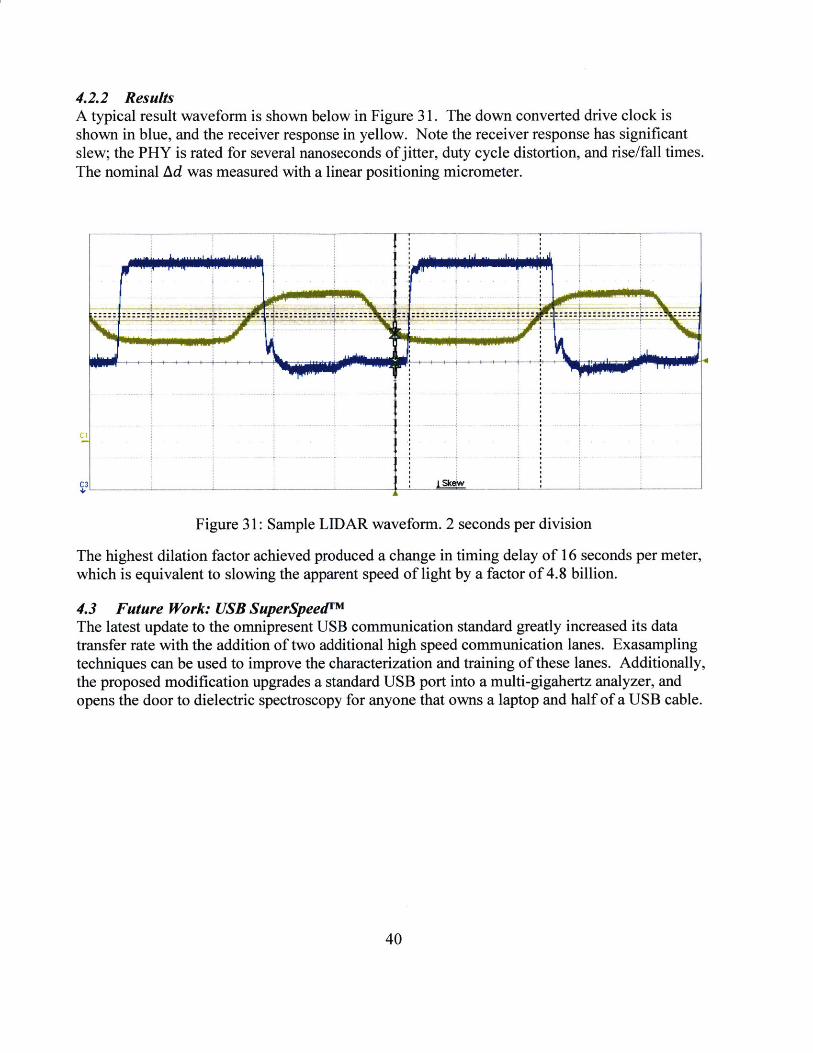
4.2.2 ResultsA typical result waveform is shown below in Figure 31. The down converted drive clock isshown in blue, and the receiver response in yellow. Note the receiver response has significantslew; the PHY is rated for several nanoseconds of jitter, duty cycle distortion, and rise/fall times.The nominal Ad was measured with a linear positioning micrometer.
C3
Figure 31: Sample LIDAR waveform. 2 seconds per division
The highest dilation factor achieved produced a change in timing delay of 16 seconds per meter,which is equivalent to slowing the apparent speed of light by a factor of 4.8 billion.
4.3 Future Work: USB SuperSpeed"mThe latest update to the omnipresent USB communication standard greatly increased its datatransfer rate with the addition of two additional high speed communication lanes. Exasamplingtechniques can be used to improve the characterization and training of these lanes. Additionally,the proposed modification upgrades a standard USB port into a multi-gigahertz analyzer, andopens the door to dielectric spectroscopy for anyone that owns a laptop and half of a USB cable.
40
IJ ... ... I...
------------............ ........ ... ---- ------
i7......... . ............. .... ..... . ............ . . ....... .. ..
............... ............... . .. ..... ...................... ... .... ................ . .. .... . ............... ..... ......... ....
.............. ..... ......... . ...................... .1 . 7 T ........................ T ...
Host
Pre-Emphasis
TX
Equalizer
RX
I A'
I I
I II I
Cable
1~
4--T
Device
Equalizer_
:>RX
Pre-Emphasis
TX
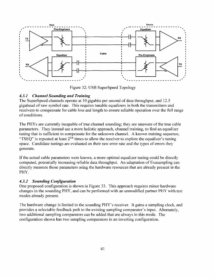
Figure 32: USB SuperSpeed Topology
4.3.1 Channel Sounding and TrainingThe SuperSpeed channels operate at 10 gigabits per second of data throughput, and 12.5gigabaud of raw symbol rate. This requires tunable equalizers in both the transmitters andreceivers to compensate for cable loss and length to ensure reliable operation over the full rangeof conditions.
The PHYs are currently incapable of true channel sounding; they are unaware of the true cableparameters. They instead use a more holistic approach, channel training, to find an equalizertuning that is sufficient to compensate for the unknown channel. A known training sequence,"TSEQ" is repeated at least 216 times to allow the receiver to explore the equalizer's tuningspace. Candidate tunings are evaluated on their raw error rate and the types of errors theygenerate.
If the actual cable parameters were known, a more optimal equalizer tuning could be directlycomputed, potentially increasing reliable data throughput. An adaptation of Exasampling candirectly measure those parameters using the hardware resources that are already present in thePHY.
4.3.2 Sounding ConfigurationOne proposed configuration is shown in Figure 33. This approach requires minor hardwarechanges in the sounding PHY, and can be performed with an unmodified partner PHY with testmodes already present.
The hardware change is limited to the sounding PHY's receiver. It gains a sampling clock, andprovides a selectable feedback path to the existing sampling comparator's input. Alternately,two additional sampling comparators can be added that are always in this mode. Theconfiguration shown has two sampling comparators in an inverting configuration.
41

- - -Pre-Emphasis
Drive Clock
TX
Equalizer
<1< F+-r
Equalizer
Pre-Emphasis Loop Back
Sampling Clock
Figure 33: Channel Sounding Configuration
Data is clocked out of the sounding PHY at fD or fD/ 2 , received by the partner PHY andimmediately retransmitted back. This is achieved with a test mode sometimes referred to as"analog loop-back" because it bypasses the digital processing and re-timing systems. It isimportant to note that the remote PHY's transmitter and transmitter equalizer are in play in thismode. The USB 3.1 spec allows for up to 1 picosecond of added jitter here.
This is now an Exasampler, albeit with a split architecture. It produces a pair of single-endedreconstructions of the differential waveform. They include the effects of the remote PHY'stransmitter equalizer, the cable, and the training PHY's receiver equalizer.
To account for potentially non-linear inter-symbol interference, the training PHY can emit atraining sequence clocked at the sample clock rate. A short 3-bit rotary grey sequence such as00011101 is recommende.
Compliance testing of a USB 3.1 channel requires an oscilloscope with at least 20 GHz ofbandwidth. This approach can perform most of those lab tests as self-tests.
42

4.3.3 Use as a Stand-Alone SensorThe sounding PHY is now a fully functional Exasampler, and can be repurposed for many of theapplications above. For example, it can perform Dielectric Spectroscopy by replacing thepartner PHY with the material of interest. A USB DS probe would simply be a connector andconductors in the desired geometry.
.. - - - - - - - - - - -P-e-mph-as- -s
Drive Clock P
Equalizer
Sampling Clock
Figure 34: Measuring milk freshness with USB dielectric spectroscopy
43

5 Conclusion and Future WorkThis thesis shows that high frequency does not necessarily mean high complexity or high cost.Digital communication components can be used to make high frequency, high fidelity analogmeasurements of stable systems.
The next major step for Exasampling is to integrate it more tightly on silicon. However, thisisn't a necessary step. These techniques are ready for immediate application and deployment. Itis a cheap and cheerful method to reduce cost and complexity for several classes of sensorsystems.
A surprising result is that the imperfections in cheap digital components actually becomebeneficial. Overshoot, ringing, and other EMI generating artifacts allow these components topush energy into high harmonics. Intentionally mistune matching networks. Use low qualitycomponents. Break things. If it is repeatable, Exasampling can pull useful information out ofthese typically undesirable effects.
The hard work has already been completed by the communication industry; they have alreadycommoditized the gigabaud. Now we can commoditize the gigahertz.
Nanoseconds for the masses.
44
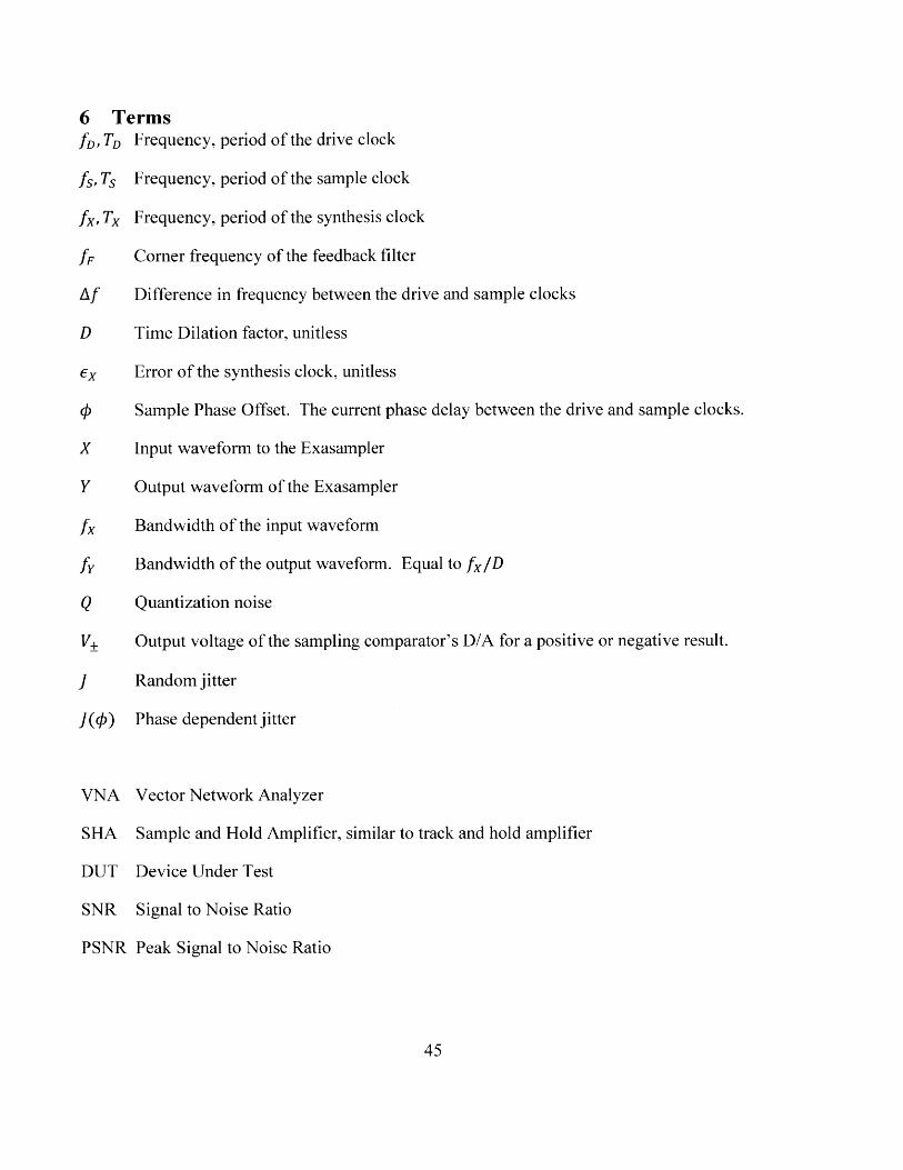
6 TermsfD, TD Frequency, period of the drive clock
fs, Ts Frequency, period of the sample clock
fx, Tx Frequency, period of the synthesis clock
fF Corner frequency of the feedback filter
Af Difference in frequency between the drive and sample clocks
D Time Dilation factor, unitless
Ex Error of the synthesis clock, unitless
0 Sample Phase Offset. The current phase delay between the drive and sample clocks.
X Input waveform to the Exasampler
Y Output waveform of the Exasampler
fx Bandwidth of the input waveform
fy Bandwidth of the output waveform. Equal to fx/D
Q Quantization noise
V Output voltage of the sampling comparator's D/A for a positive or negative result.
J Random jitter
J(O) Phase dependent jitter
VNA Vector Network Analyzer
SHA Sample and Hold Amplifier, similar to track and hold amplifier
DUT Device Under Test
SNR Signal to Noise Ratio
PSNR Peak Signal to Noise Ratio
45

7 Bibliography
[1] M. Marino, "Executive arrested in taiwan cooking oil scandal," Olive Oil Times, 24October 2014.
[2] M. A. Sairin, S. A. Aziz, N. N. A. Nizar, N. A. A. Latiff, A. Ismail, D. M. Hashim and F.Z. Rokhani, "Lard Detection in Edible Oil Using Dielectric Spectroscopy," in SensorsforEveryday Life, 2016, pp. 245-271.
[3] S. 0. Nelson, "Agricultural Applications of Dielectric Spectroscopy," Journal ofMicrowave Power and Electromagnetic Energy, pp. 75-85, 39:2 2004.
[4] S. 0. Nelson, "Dielectric Spectroscopy of Fresh Fruit and Vegetable Tissues from 10 to1800 MHz," Journal of Microwave Power and Electromagnetic Energy, pp. 31-47, 40:12005.
[5] P. Mohr, U. Birgersson, C. Berking, C. Henderson, U. Trefzer, L. Kemeny, C.Sunderkotter, T. Dirschka, R. Motley, M. Frohm-Nilsson, U. Reinhold, C. Loquai, R.Braun, F. Nyberg and J. Paoli, "Electrical impedance spectroscopy as a potential adjunctdiagnostic tool for cutaneous melanoma," Skin Research & Technology, pp. 75-83, 27January 2013.
[6] R. P. Henderson and J. G. Webster, "An Impedance Camera for Spatially SpecificMeasurements of the Thorax," IEEE Transactions on Biomedical Engineering, pp. 250-254, May 1978.
[7] T. A. Hope and S. E. Iles, "Technology review: The use of electrical impedance scanningin the detection of breast cancer," Breast Cancer Research, pp. 69-74, 13 November 2003.
[8] R. J. Halter and Y.-J. Kim, "Toward Microendoscopic Electrical Impedance Tomographyfor Intraoperative Surgical Margin Assessment," IEEE Transactions BiomedicalEngineering, pp. 2779-2786, November 2014.
[9] L. Hoffmann, C. Gautier, S. Lefebvre and F. Costa, "Thermal measurement of losses ofGaN power transistors for optimization of their drive," in Power Electronics andApplications, Lille, France, 2013.
[10] D. Berning and A. Hefner, "IGBT half-bridge shoot-through characterization for modelvalidation," Industry Applications Conference, pp. 1491-1499, 6 October 1996.
46

[11] Peregrine Semiconductor, "PE29 100 Product Specification," 01 08 2016. [Online].Available: http://www.psemi.com/pdf/datasheets/pe291 00ds.pdf. [Accessed 5 11 2016].
[12] H. C. P. Dymond, "Reduction of oscillations in a GaN bridge leg using active gate drivingwith sub-ns resolution, arbitrary gate-impedance patterns," IEEE ECCE, 2016.
[13] C. E. Shannon, "Communication in the Presence of Noise," Proceedings of the IRE, pp.10-21, January 1949.
[14] S. v. T. E. Louwsma and B. Nauta, Time-interleaved Analog-to-Digital Converters,Springer, 2011.
[15] B. Razavi, "Design of Sample-and-Hold Amplifiers for High-Speed Low-Voltage A/DConverters," CICC, pp. 59-66, 1997.
[16] P. J. Pupalaikis, B. Yamrone, R. Delbue, A. S. Khanna, K. Doshi, B. Bhat and A. Sureka,"Technologies for Very High Bandwidth Real-time Oscilloscopes," IEEE BIPOLARBICMOS CIRCUITS AND TECHNOLOGY MEETING, p. 9, 2014.
[17] Analog Devices, "AD9578 Dual Precision PLL Synthesizer," [Online]. Available:http://www.analog.com/en/products/clock-and-timing/clock-generation-distribution/ad9578.html. [Accessed 6 12 2016].
[18] E. Yflce, "All-optical switching of a microcavity repeated at terahertz rates," OpticsLetters, pp. 374-376, 2013.
[19] P. J. Pupalaikis, "Random Interleaved Sampling," [Online]. Available:http://cdn.teledynelecroy.com/files/whitepapers/wpris_102203.pdf. [Accessed 3 11 2016].
[20] T.-i. Otsuji, "A Picosecond Accuracy, 700MHz Range, Si-Bipolar Time Interval CounterLSI," IEEE Journal ofSolid-State Circuits, pp. 941-947, 1993.
[21] J. Kalisz, "Review of Methods for time interval measurements with picosecondresolution," Metrologia, pp. 17-32, 2003.
[22] M. Zieliiski, "Architecture of the multi-tap-delay-line time-interval measurement moduleimplemented in FPGA device," ACTA IMEKO, pp. 77-81, 2015.
[23] K. Poulton, "Architectures and Issues for Gigasample/second ADCs," AA CD, pp. 1-18,2006.
[24] M. Patel, I. Darwazeh and J. O'Reilly, "Bandpass sampling for software radio receivers,and the effect of oversampling on aperture jitter," in Vehicular Technology Conference,
47
Birmingham, 2002.
[25] W. Kester, "ADC Architectures III: Sigma-Delta ADC Basics," 1 10 2008. [Online].Available: http://www.analog.com/media/en/training-seminars/tutorials/MT-022.pdf.[Accessed 5 11 2016].
[26] F. de Jager, "Delta Modulation: A Method of PCM Transmission Using the One UnitCode," Philips Research Reports, p. Vol 7, 7 1952.
[27] C. Culter.United States of America Patent 2,927,962, 1960.
[28] Analog Devices, "ADCMP600/ADCMP601/ADCMP602," 14 February 2017. [Online].Available: http://www.analog.com/media/en/technical-documentation/data-sheets/ADCMP600_60 1_602.pdf.
[29] J. E. Abate, "Linear and Adaptive Delta Modulation," Proceedings of the IEEE, pp. 298-308, No 3 Vol 55 1967.
[30] "Idle tone behavior in Sigma Delta Modulation," in Audio Engineering Society, Vienna,2007.
[31] Analog Devices, "ADCMP572/ADCMP573 Ultrafast 3.3 V/5 V Single-Supply SiGeComparators," [Online]. Available: http://www.analog.com/media/en/technical-documentation/data-sheets/ADCMP572_573.pdf.
[32] Cypress Semiconductor Corporation, "PSoC® 5LP: CY8C58LP Family Datasheet," SanJose, CA.
[33] Hewlett Packard, "Application Note 918: Pulse and Waveform Generation with StepRecovery Diodes," Palo Alto, 84.
[34] D. Bowman, "Source 2," 2005. [Online]. Available: http://www.g0mrf.com/source2.htm.
[35] B. Razavi, "A Study of Injection Locking and Pulling in Oscillators," IEEE JOURNAL OFSOLID-STA TE CIRCUITS, pp. 1415-1424, 2004.
[36] Agilent, "Basics of Measuring the Dielectric Properties of Materials," 2005.
[37] Agilent, "Microwave Dielectric Spectroscopy Workshop," 2004.
[38] A. Kadambi, H. Zhao, B. Shi and R. Raskar, "Occluded Imaging with Time-of-FlightSensors," A CM Trans. Graph, vol. 35, no. 2, p. 12, 2016.
48

[39] Broadcom, "Broadcom," 2013. [Online]. Available:https://docs.broadcom.com/docs/AV02-2701 EN.
[40] D. Rytting, "ARFTG 50 Year Network Analyzer History," in ARFTG MicrowaveMeasurement Conference, Atlanta, GA, 2008.
[41] S. 0. Nelson, "Agricultural Applications of Dielectric Spectroscopy," Journal ofMicrowave Power and Electromagnetic Energy, pp. 75-85, 2004.
[42] USB IF, "USB 3.0 SuperSpeed Equalizer Design Guidelines," 10 6 2011. [Online].Available:http://www.usb.org/developers/docs/whitepapers/USBSuperspeedEqualizerDesignGuidelines_2011-06-10.pdf.
[43] J. Williams, Analog Circuit Design: Art, Science, and Personalities, Butterworth-Heinemann, 1991.
[44] Avago Technologies, "HSMP-382x, 482x Surface Mount RF PIN Switch and LimiterDiodes," 9 April 2017. [Online]. Available:https://www.broadcom.com/products/wireless/diodes/pin/hsmp-3 822.
[45] USB IF, "Universal Serial Bus 3.1 Specification," 2013.
[46] D. L. J. W. J. D. N. M. D. P. S. J. H. B. H. S. H. C. P. Dymond, "Reduction of oscillationsin a GaN bridge leg using active gate driving with sub-ns resolution, arbitrary gate-impedance patterns," IEEE ECCE, 2016.
[47] G. C. J. C. E. D. R. D. B. B. d. R. A. P. M. J.-M. G. a. W. L. V. Emre Yflce, "All-opticalswitching of a microcavity repeated at terahertz rates," Optics Letters, pp. 374-376, 2013.
49