nanoscale joule heating, peltier cooling and current crowding at
TRANSCRIPT
Nanoscale Joule heating, Peltier cooling andcurrent crowding at graphene–metal contactsKyle L. Grosse1,2, Myung-Ho Bae2,3, Feifei Lian2,3, Eric Pop2,3,4* and William P. King1,2,4,5*
The performance and scaling of graphene-based electronics1 islimited by the quality of contacts between the graphene andmetal electrodes2–4. However, the nature of graphene–metalcontacts remains incompletely understood. Here, we useatomic force microscopy to measure the temperature distri-butions at the contacts of working graphene transistors witha spatial resolution of ∼10 nm (refs 5–8), allowing us to ident-ify the presence of Joule heating9–11, current crowding12–16
and thermoelectric heating and cooling17. Comparison withsimulation enables extraction of the contact resistivity (150–200 Vmm2) and transfer length (0.2–0.5 mm) in our devices;these generally limit performance and must be minimized.Our data indicate that thermoelectric effects account for upto one-third of the contact temperature changes, and thatcurrent crowding accounts for most of the remainder.Modelling predicts that the role of current crowding will dimin-ish and the role of thermoelectric effects will increase ascontacts improve.
The physical phenomena primarily responsible for changes inthe temperature of semiconductor devices during electrical oper-ation are the Joule and Peltier effects. The Joule effect9 occurs ascharge carriers dissipate energy within the lattice, and is pro-portional to resistance and the square of the current. The Peltiereffect17 is proportional to the magnitude of the current throughand the difference in thermopower at a junction of dissimilarmaterials, leading to either heating or cooling depending on thedirection of current flow. A rise in temperature negatively affectselectronic devices, decreasing performance by lowering carriermobility10 and reducing the device lifetime18.
Joule heating in graphene transistors results in a local tempera-ture rise (‘hot spot’)11,19; the position of this corresponds to thecarrier density minimum and its shape has been linked to thedensity of states11. In contrast, thermal phenomena at graphene–metal contacts are not well understood, although thermoelectriceffects play a role at monolayer–bilayer interfaces20. Given that thethermopower of graphene can reach S ≈ 100 mV K21 slightlyabove room temperature21–23, Peltier contact effects could be signifi-cant in future graphene electronics under normal operating con-ditions. Moreover, little is known about transport at graphenecontacts, although they are clearly recognized as a fundamentalroadblock for graphene nanoelectronics2–4.
Here, we use atomic force microscopy (AFM)-based temperaturemeasurements5–8 with a spatial resolution of 10 nm and tempera-ture resolution of 250 mK, combined with detailed simulations, touncover not only the effects of Joule heating, but also to revealPeltier cooling and current crowding at graphene–metal contacts.These effects are key to understanding the scalability and ultimate
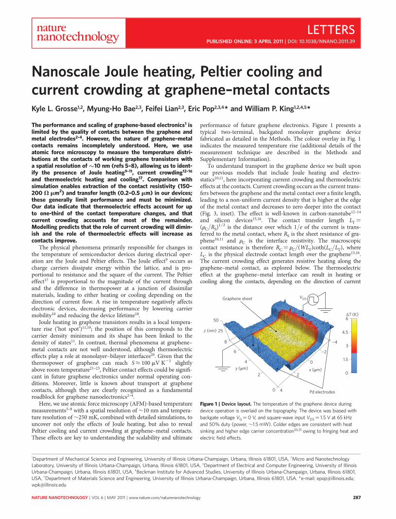
performance of future graphene electronics. Figure 1 presents atypical two-terminal, backgated monolayer graphene devicefabricated as detailed in the Methods. The colour overlay in Fig. 1indicates the measured temperature rise (additional details of themeasurement technique are described in the Methods andSupplementary Information).
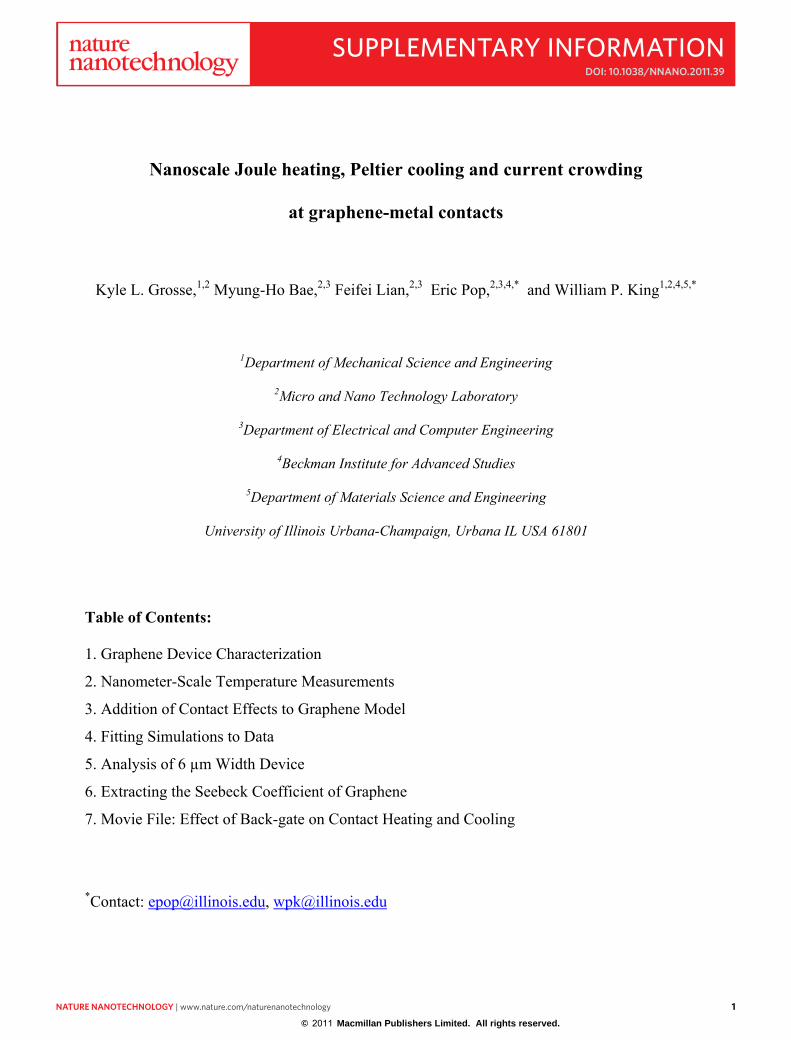
To understand transport in the graphene device we built uponour previous models that include Joule heating and electro-statics10,11, here incorporating current crowding and thermoelectriceffects at the contacts. Current crowding occurs as the current trans-fers between the graphene and the metal contact over a finite length,leading to a non-uniform current density that is higher at the edgeof the metal contact and decreases to zero deeper into the contact(Fig. 3, inset). The effect is well-known in carbon-nanotube12–14
and silicon devices15,16. The contact transfer length LT¼(rC/RS)1/2 is the distance over which 1/e of the current is trans-ferred to the metal contact, where RS is the sheet resistance of gra-phene10,11 and rC is the interface resistivity. The macroscopiccontact resistance is therefore RC¼ rC/(WLT)coth(LC/LT), whereLC is the physical electrode contact length over the graphene15,16.The current crowding effect generates resistive heating along thegraphene–metal contact, as explored below. The thermoelectriceffect at the graphene–metal interface can result in heating orcooling along the contacts, depending on the direction of current
6
4.5
3
1.5
02
4
4
6
8
25
50
2
0
0
−2
−4
Graphene sheet
Pd electrodes
z (nm)
VDS
ΔT (K)
x (μm)y (μm)
Figure 1 | Device layout. The temperature of the graphene device during
device operation is overlaid on the topography. The device was biased with
backgate voltage VG¼0 V, and square-wave input VDS¼ 1.5 V at 65 kHz
and 50% duty (power, 1.5 mW). Colder edges are consistent with heat
sinking and higher edge carrier concentration30,31 owing to fringing heat and
electric field effects.
1Department of Mechanical Science and Engineering, University of Illinois Urbana-Champaign, Urbana, Illinois 61801, USA, 2Micro and NanotechnologyLaboratory, University of Illinois Urbana-Champaign, Urbana, Illinois 61801, USA, 3Department of Electrical and Computer Engineering, University of IllinoisUrbana-Champaign, Urbana, Illinois 61801, USA, 4Beckman Institute for Advanced Studies, University of Illinois Urbana-Champaign, Urbana, Illinois 61801,USA, 5Department of Materials Science and Engineering, University of Illinois Urbana-Champaign, Urbana, Illinois 61801, USA. *e-mail: [email protected];[email protected]
LETTERSPUBLISHED ONLINE: 3 APRIL 2011 | DOI: 10.1038/NNANO.2011.39
NATURE NANOTECHNOLOGY | VOL 6 | MAY 2011 | www.nature.com/naturenanotechnology 287
flow and the sign of the Seebeck coefficient S. Here, S is calculated ateach point along the metal–graphene contacts self-consistently withthe charge density, potential and contact temperature (details ofcurrent crowding and thermoelectric implementation are describedin the Supplementary Information).
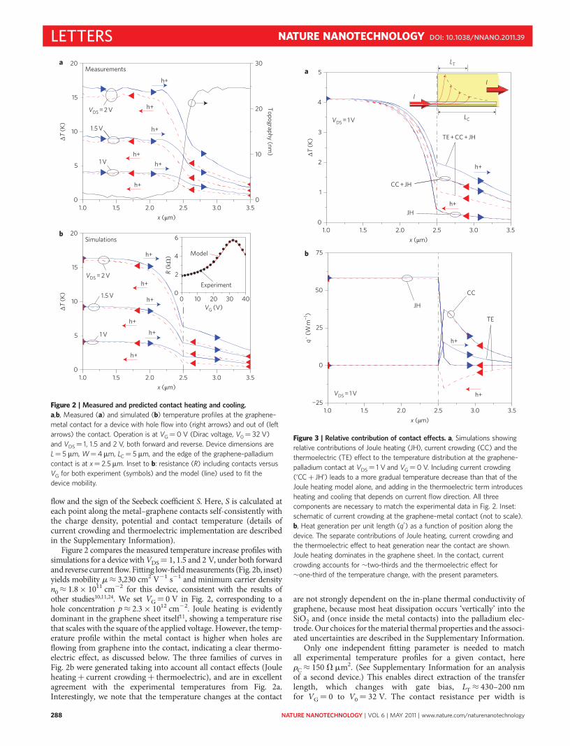
Figure 2 compares the measured temperature increase profiles withsimulations for a device with VDS¼ 1, 1.5 and 2 V, under both forwardand reverse current flow. Fitting low-field measurements (Fig. 2b, inset)yields mobility m≈ 3,230 cm2 V21 s21 and minimum carrier densityn0 ≈ 1.8× 1011 cm22 for this device, consistent with the results ofother studies10,11,24. We set VG¼ 0 V in Fig. 2, corresponding to ahole concentration p ≈ 2.3 × 1012 cm22. Joule heating is evidentlydominant in the graphene sheet itself11, showing a temperature risethat scales with the square of the applied voltage. However, the temp-erature profile within the metal contact is higher when holes areflowing from graphene into the contact, indicating a clear thermo-electric effect, as discussed below. The three families of curves inFig. 2b were generated taking into account all contact effects (Jouleheatingþ current crowdingþ thermoelectric), and are in excellentagreement with the experimental temperatures from Fig. 2a.Interestingly, we note that the temperature changes at the contact
are not strongly dependent on the in-plane thermal conductivity ofgraphene, because most heat dissipation occurs ‘vertically’ into theSiO2 and (once inside the metal contacts) into the palladium elec-trode. Our choices for the material thermal properties and the associ-ated uncertainties are described in the Supplementary Information.
Only one independent fitting parameter is needed to matchall experimental temperature profiles for a given contact, hererC ≈ 150 Vmm2. (See Supplementary Information for an analysisof a second device.) This enables direct extraction of the transferlength, which changes with gate bias, LT ≈ 430–200 nmfor VG¼ 0 to V0¼ 32 V. The contact resistance per width is
a
b
Measurements
h+
h+ Topography (nm)
15
20
10 h+1.5 V
h+
5
0
4
6Simulations
h+ Model
2VDS = 2 V
VDS = 2 V
R (kΩ
)
0 10 20 30 400
h+
h+1.5 V
Experiment
ΔT (K
)
h+
1 V
1 V
VG (V)
h+
h+
h+
h+
1.0 2.01.5 2.5 3.0 3.5x (μm)
1.0 2.01.5 2.5 3.0 3.5x (μm)
15
20
10
5
0
ΔT (K
)30
20
10
0
Figure 2 | Measured and predicted contact heating and cooling.
a,b, Measured (a) and simulated (b) temperature profiles at the graphene–
metal contact for a device with hole flow into (right arrows) and out of (left
arrows) the contact. Operation is at VG¼0 V (Dirac voltage, V0¼ 32 V)
and VDS¼ 1, 1.5 and 2 V, both forward and reverse. Device dimensions are
L¼ 5 mm, W¼ 4 mm, LC¼ 5 mm, and the edge of the graphene–palladium
contact is at x¼ 2.5mm. Inset to b: resistance (R) including contacts versus
VG for both experiment (symbols) and the model (line) used to fit the
device mobility.
5a
I
I
VDS = 1 V
3TE + CC + JH
LC
LT
2
ΔT (K
)
h+
1CC + JH
h+
0JH
75b
50 CC
25
JH
TE
q´ (W
m−1
)
0
1.0 1.5 2.0 2.5−25
h+
h+
VDS = 1 V
3.0 3.5x (μm)
1.0 1.5 2.0 2.5 3.0 3.5x (μm)
4
Figure 3 | Relative contribution of contact effects. a, Simulations showing
relative contributions of Joule heating (JH), current crowding (CC) and the
thermoelectric (TE) effect to the temperature distribution at the graphene–
palladium contact at VDS¼ 1 V and VG¼0 V. Including current crowding
(‘CCþ JH’) leads to a more gradual temperature decrease than that of the
Joule heating model alone, and adding in the thermoelectric term introduces
heating and cooling that depends on current flow direction. All three
components are necessary to match the experimental data in Fig. 2. Inset:
schematic of current crowding at the graphene–metal contact (not to scale).
b, Heat generation per unit length (q′) as a function of position along the
device. The separate contributions of Joule heating, current crowding and
the thermoelectric effect to heat generation near the contact are shown.
Joule heating dominates in the graphene sheet. In the contact, current
crowding accounts for two-thirds and the thermoelectric effect for
one-third of the temperature change, with the present parameters.
LETTERS NATURE NANOTECHNOLOGY DOI: 10.1038/NNANO.2011.39
NATURE NANOTECHNOLOGY | VOL 6 | MAY 2011 | www.nature.com/naturenanotechnology288

RCW ≈ 350–750 Vmm over this range, about a factor of two lowerfor our thin chromium (0.5 nm)/palladium contacts than previousreports (which used thicker chromium (15 nm)/gold, titanium(10 nm)/gold, or nickel2,3). Nevertheless, the relatively largeLT has profound consequences for device scaling, as contactlength LC . LT (on the order of 1 mm) must be chosen tominimize RC in sub-100 nm graphene devices. The size of thecontacts would therefore dwarf the size of the channel itself. In com-parison, the typical contact resistance of modern silicon devices is100 Vmm, achieved with contacts of ,100 nm (refs 25,26).
Figure 3a shows temperature rise predictions including only Jouleheating, then adding in current crowding and then the thermoelec-tric effect. When only Joule heating is considered, there is a sharptemperature drop in the electrode, which acts as a heat sink. Thecurrent crowding term introduces additional heating into the elec-trode. Finally, the inclusion of the thermoelectric effect generates atemperature asymmetry (heating versus cooling) with respect tocarrier flow direction. The thermoelectric effect is evident as a differ-ence in temperature when the current flow is reversed, shown in Figs2 and 3. At VDS¼ 1 V, the thermoelectric effect cools one electrodeby0.5 K (30%) under carrier outflow, and heats the opposite elec-trode similarly under carrier inflow. To understand the individualcontributions of Joule heating, current crowding and the thermoelec-tric effect within the contact, Fig. 3b shows their separate heat gener-ation rates, with the thermoelectric effect less than zero under holeflow from contact to graphene.
Figure 4 further explores how the thermoelectric effect affectstemperature rise within the contact. Here, we define the temperatureasymmetry as DTASM¼ DT( jþ) 2 DT( j2), the maximum differ-ence in temperature rise between the two current flow directions(Supplementary Fig. S6). Figure 4a compares DTASM for a simu-lation to experimental results at VDS¼ 1 V, again highlighting thedominant role played by the thermoelectric effect. DTASM changessign when the gate voltage is swept through V0, as the sign of thegraphene thermopower changes when majority carriers switchfrom holes to electrons20–23. Joule heating and current crowdingeffects make insignificant contributions to the temperatureasymmetry when the local graphene sheet resistance (RS) changeswith gate bias. (See Supplementary movie for further illustrationof these transitions.) In addition, a comparison of our simulationswith the temperature data from Fig. 4a allows an independentextraction of the thermopower (S ≈ 63 mV K21 at VG 2
V0¼225 V), which is in good agreement with previous valuesmeasured for monolayer graphene (see SupplementaryInformation)22,23. Figure 4b presents the temperature asymmetrywith respect to current flow, indicating that at intermediatecurrent density it can reach several degrees kelvin. Such temperaturechanges can affect long-term device reliability18, and could be evenmore important in submicrometre graphene devices, which areessentially dominated by their contacts.
The panels in Fig. 4c,d examine the absolute temperature rise atthe contacts in improved future graphene devices, for which we
a b
c d3Future device
2
1
0ΔT (K
)
−1
ΔTC,MIN
ΔTC,MAX
Present device
−30 −20 −10 0 10 20 30−2
VG − V0 (V)
20 Future device
16 VDS = 2 V
12 1.5 V
8
41 VΔT
(K)
h+0
−5.0 −2.5 0.0 2.5 5.0−4
x (μm)
VG − V0 = −30 V
1.6
0.8Experiment
TE + CC + JH
0.0
CC + JH−0.8
−1.6VDS = 1 V
ΔTA
SM (K
)
−30 −20 −10 0 10 20 30VG − V0 (V)
6IDS = 150 μA μm−1
4
2
0
−2100
50−4
−6
ΔTA
SM (K
)
−30 −20 −10 0 10 20 30VG − V0 (V)
Figure 4 | Contact temperature under varying conditions. a, Comparison of predicted and measured temperature asymmetry DTASM at VDS¼ 1 V. DTASM is
the maximum difference in temperature rise of the contact for forward and reverse current flows (Supplementary Fig. S6). Joule heating and current
crowding effects are negligible, and the thermoelectric effect dominates the temperature asymmetry and can be used to extract the Seebeck coefficient
(see main text and Supplementary Information). b, Predictions of DTASM as a function of current density. c, Contact temperature rise for the present
device (rC¼ 150 Vmm2, m¼ 3,230 cm2 V21 s21) and a future device with greatly improved contact resistance and mobility (rC¼ 1 Vmm2,
m¼ 2 × 104 cm2 V21 s21) at VDS¼ 1 V. The maximum and minimum temperature rises at the contacts are indicated by DTC,MAX and DTC,MIN, and the gap
between the two curves is DTASM, shown by the arrows. The temperature changes owing to the thermoelectric effect at the contacts are enhanced in future
devices. d, Projected temperature profile along the channel of a 5-mm-long device with the improved parameters. Note the negative temperature change at
the right contact, where the current crowding is now negligible and the thermoelectric cooling becomes dominant.
NATURE NANOTECHNOLOGY DOI: 10.1038/NNANO.2011.39 LETTERS
NATURE NANOTECHNOLOGY | VOL 6 | MAY 2011 | www.nature.com/naturenanotechnology 289

expect higher mobility and reduced contact resistivity. The ‘presentdevice’ uses the simulation parameters fit to the experiments athand. The ‘future projection’ assumes a desirable ‘good perform-ance’ on SiO2 of m¼ 2 × 104 cm2 V21 s21 and rC¼ 1 Vmm2. Wefind that such improvements in device quality tend to enhance ther-moelectric contact asymmetry. The increase in mobility anddecrease in contact resistivity both lead to a shorter transferlength LT, and enhancement of the electric field at the contact.This, in turn, leads to an increase in the temperature and potentialgradient (field), enhancing the thermoelectric effect at the contacts.
In summary, we have used an AFM thermal imaging techniqueto observe temperature distributions at graphene–metal contactswith unprecedented spatial and temperature resolution. Theobserved temperature distributions can be explained only with a sig-nificant thermoelectric effect, combined with current crowding andJoule heating. Projections based on simulations fit to our initialexperiments suggest that, with technology scaling and improve-ment, the roles of contact resistance and current crowding willdiminish, whereas the role of thermoelectric contact effects willbecome more significant for future graphene nanoelectronics.
MethodsSample fabrication. Graphene was mechanically exfoliated10,11 on 300 nm thermalSiO2 with highly n-doped silicon as the backgate. Samples were annealed in achemical vapour deposition chamber with argon/hydrogen at 400 8C for 35 minbefore and after graphene deposition27. Electron-beam lithography was used topattern the electrodes and shape the graphene sheets. Chromium/palladium(0.5 nm/40 nm) source and drain electrodes were evaporated, followed by an oxygenplasma etch to define the device shape. Single-layer graphene was confirmed withRaman spectroscopy28,29, and electrode thickness was verified by AFM scan. Forthermal AFM measurements, a 65 nm layer of poly(methyl methacrylate) (PMMA)was spun onto the device8, with the thickness confirmed by ellipsometry. ThePMMA served to amplify the thermal signal for the AFM temperaturemeasurements, and to protect the samples from spurious doping effects duringmeasurements. Complete data for two devices are presented in detail here and in theSupplementary Information, from a total of six devices tested, all of which yieldedsimilar results.
Thermal AFM measurement. Scanning Joule expansion microscopy (SJEM)5–8 wasused to measure the temperature rise during device operation. Device heating wasinduced with a 65 kHz, 50% duty square wave with amplitude VDS.Thermomechanical expansion of the sample was measured by monitoring thecantilever deflection signal with a lock-in amplifier technique. Each temperatureprofile shown was averaged over 128 line scans, each 3 mm long, across thegraphene–electrode junction. The measurement could be improved with longerscans, but was limited here to avoid Dirac voltage shift under prolonged electricalstress. Additional details regarding setup and calibration of the SJEM experiment areavailable in the Supplementary Information.
Received 27 January 2011; accepted 24 February 2011;published online 3 April 2011
References1. Schwierz, F. Graphene transistors. Nature Nanotech. 5, 487–496 (2010).2. Nagashio, K., Nishimura, T., Kita, K. & Toriumi, A. Systematic investigation of
the intrinsic channel properties and contact resistance of monolayer andmultilayer graphene field-effect transistor. Jpn J. Appl. Phys. 49, 051304 (2010).
3. Nagashio, K., Nishimura, T., Kita, K. & Toriumi, A. Contact resistivity andcurrent flow path at metal/graphene contact. Appl. Phys. Lett. 97, 143514 (2010).
4. Khomyakov, P. A., Starikov, A. A., Brocks, G. & Kelly, P. J. Nonlinear screeningof charges induced in graphene by metal contacts. Phys. Rev. B 82,115437 (2010).
5. Varesi, J. & Majumdar, A. Scanning Joule expansion microscopy at nanometerscales. Appl. Phys. Lett. 72, 37–39 (1998).
6. Majumdar, A. & Varesi, J. Nanoscale temperature distributions measured byscanning Joule expansion microscopy. J. Heat Transfer 120, 297–305 (1998).
7. Cannaerts, M., Buntinx, D., Volodin, A. & Van Haesendonck, C. Calibration of ascanning Joule expansion microscope (SJEM). Appl. Phys. A 72, S67–S70 (2001).
8. Gurrum, S. P., King, W. P., Joshi, Y. K. & Ramakrishna, K. Size effect on thethermal conductivity of thin metallic films investigated by scanning Jouleexpansion microscopy. J. Heat Transfer 130, 082403 (2008).
9. Pop, E. Energy dissipation and transport in nanoscale devices. Nano Res. 3,147–169 (2010).
10. Dorgan, V. E., Bae, M-H. & Pop, E. Mobility and saturation velocity in grapheneon SiO2. Appl. Phys. Lett. 97, 082112 (2010).
11. Bae, M-H., Ong, Z-Y., Estrada, D. & Pop, E. Imaging, simulation, andelectrostatic control of power dissipation in graphene devices. Nano Lett. 10,4787–4793 (2010).
12. Jackson, R. & Graham, S. Specific contact resistance at metal/carbon nanotubeinterfaces. Appl. Phys. Lett. 94, 012109 (2009).
13. Lan, C. et al. Measurement of metal/carbon nanotube contact resistance byadjusting contact length using laser ablation. Nanotechnology 19, 125703 (2008).
14. Franklin, A. D. & Chen, Z. Length scaling of carbon nanotube transistors. NatureNanotech. 5, 858–862 (2010).
15. Schroder, D. K. Semiconductor Material and Device Characterization(Wiley, 2006).
16. Chieh, Y. S., Perera, A. K. & Krusius, J. P. Series resistance of silicided ohmiccontacts for nanoelectronics. IEEE Trans. Electron. Dev. 39, 1882–1888 (1992).
17. DiSalvo, F. J. Thermoelectric cooling and power generation. Science 285,703–706 (1999).
18. Schroder, D. K. & Babcock, J. A. Negative bias temperature instability: road tocross in deep submicron silicon semiconductor manufacturing. J. Appl. Phys. 94,1–18 (2003).
19. Freitag, M., Chiu, H-Y., Steiner, M., Perebeinos, V. & Avouris, P. Thermalinfrared emission from biased graphene. Nature Nanotech. 5, 497–501 (2010).
20. Xu, X., Gabor, N. M., Alden, J. S., van der Zande, A. M. & McEuen, P. L.Photo-thermoelectric effect at a graphene interface junction. Nano Lett. 10,562–566 (2009).
21. Wei, P., Bao, W., Pu, Y., Lau, C. N. & Shi, J. Anomalous thermoelectric transportof Dirac particles in graphene. Phys. Rev. Lett. 102, 166808 (2009).
22. Zuev, Y. M., Chang, W. & Kim, P. Thermoelectric and magnetothermoelectrictransport measurements of graphene. Phys. Rev. Lett. 102, 096807 (2009).
23. Checkelsky, J. G. & Ong, N. P. Thermopower and Nernst effect in graphene in amagnetic field. Phys. Rev. B 80, 081413 (2009).
24. Zhu, W., Perebeinos, V., Freitag, M. & Avouris, P. Carrier scattering, mobilities,and electrostatic potential in monolayer, bilayer, and trilayer graphene. Phys.Rev. B 80, 235402 (2009).
25. International Technology Roadmap for Semiconductors (ITRS), http://public.itrs.net (2009).
26. Thompson, S. E. et al. In search of ‘Forever,’ continued transistor scaling onenew material at a time. IEEE Trans. Semicond. Manuf. 18, 26–36 (2005).
27. Ishigami, M., Chen, J. H., Cullen, W. G., Fuhrer, M. S. & Williams, E. D. Atomicstructure of graphene on SiO2. Nano Lett. 7, 1643–1648 (2007).
28. Koh, Y. H., Bae, M.-H., Cahill, D. G. & Pop, E. Reliably counting atomic planesof few-layer graphene (n . 4). ACS Nano 5, 269–274 (2011).
29. Malard, L. M., Pimenta, M. A., Dresselhaus, G. & Dresselhaus, M. S. Ramanspectroscopy in graphene. Phys. Rep. 473, 51–87 (2009).
30. Silvestrov, P. G. & Efetov, K. B. Charge accumulation at the boundaries of agraphene strip induced by a gate voltage: electrostatic approach. Phys. Rev. B77, 155436 (2008).
31. Vasko, F. T. & Zozoulenko, I. V. Conductivity of a graphene strip: width andgate-voltage dependencies. Appl. Phys. Lett. 97, 092115 (2010).
AcknowledgementsThis work was supported by the Air Force Office of Scientific Research MURI FA9550-08-1-0407, Office of Naval Research grants N00014-07-1-0767, N00014-09-1-0180 andN00014-10-1-0061, and the Air Force Young Investigator Program (E.P.).
Author contributionsK.L.G. performed measurements and simulations. M-H.B. fabricated devices and assistedwith simulations. E.P. implemented the computational model and physical interpretation,with help from F.L., while E.P. and W.P.K. conceived the experiments. All authors discussedthe results. K.L.G., E.P. and W.P.K. co-wrote the manuscript.
Additional informationThe authors declare no competing financial interests. Supplementary informationaccompanies this paper at www.nature.com/naturenanotechnology. Reprints andpermission information is available online at http://npg.nature.com/reprintsandpermissions/.Correspondence and requests for materials should be addressed to E.P. and W.P.K.
LETTERS NATURE NANOTECHNOLOGY DOI: 10.1038/NNANO.2011.39
NATURE NANOTECHNOLOGY | VOL 6 | MAY 2011 | www.nature.com/naturenanotechnology290
SUPPLEMENTARY INFORMATIONdoi: 10.1038/nnano.2011.39
nature nanotechnology | www.nature.com/naturenanotechnology 1
1
Supplementary Information
Nanoscale Joule heating, Peltier cooling and current crowding
at graphene-metal contacts
Kyle L. Grosse,1,2 Myung-Ho Bae,2,3 Feifei Lian,2,3 Eric Pop,2,3,4,* and William P. King1,2,4,5,*
1Department of Mechanical Science and Engineering
2Micro and Nano Technology Laboratory
3Department of Electrical and Computer Engineering
4Beckman Institute for Advanced Studies
5Department of Materials Science and Engineering
University of Illinois Urbana-Champaign, Urbana IL USA 61801
Table of Contents:
1. Graphene Device Characterization
2. Nanometer-Scale Temperature Measurements
3. Addition of Contact Effects to Graphene Model
4. Fitting Simulations to Data
5. Analysis of 6 µm Width Device
6. Extracting the Seebeck Coefficient of Graphene
7. Movie File: Effect of Back-gate on Contact Heating and Cooling
*Contact: [email protected], [email protected]
© 2011 Macmillan Publishers Limited. All rights reserved.

2 nature nanotechnology | www.nature.com/naturenanotechnology
SUPPLEMENTARY INFORMATION doi: 10.1038/nnano.2011.39
1. GrapR
the graphthe 2D pphene demaximummonolayand Fig. tral (Diratively. D
Figure S(length L
Figure ScantileveThe sampriodic wamo-mechusing a c
24100
200
300
400
500
600
700
Inte
nsity
(A.U
.)
a
hene DevicRaman specthene transistpeak of the Revices (633 nm (fwhm) ofer graphene.S5(b) (W =
ac) voltage fetermination
S1 | Raman L = 5 µm, wi
S2 | Experimer deflectionple experienaveform supphanical expaconstant volt
400 2500Ra
4 μm Devic
Lorentzia
Measurem
ce Charactroscopy andors used in tRaman measnm, 1.7 mWf 31.6 and 2.1-3 Electron6 µm) with
for the W = 4n of carrier m
spectroscopydth W = 4 a
mental Setups using a laces periodicplied to the nsion. The b
tage source t
0 2600
aman Shift (c
ce
an Fit
ments
terizationd two-probe this study. Fisurement for
W laser). The28.9 cm-1 fornic measuremgraphene re4 and 6 µm mobility and
py. 2D Ramand 6 µm). Si
p. An atomiaser-photodic thermo-mesample. A lo
back-gate vothat shares a
2700 28cm-1)
2
electrical migures S1(a)r length L =e 2D peak shr the two devments are shsistance R asamples wacarrier pudd
an peaks for ingle Lorent
ic force micriode system chanical expock-in amplifoltage VG is aa common gr
800
2400100
200
300
400
500
600
700
Inte
nsity
(A.U
.)
b 6
M
measuremen) and (b) sho= 5 µm and hift of ~265vices is con
hown in the is a function s measured dle density i
r two graphetzian fit conf
roscope (AFand by ope
pansions dueifier techniquapplied to thround with t
0 2500Rama
6 μm Device
Lorentzian
Measureme
nts were useow the single
width W = 0 cm-1 and
nsistent with inset of Fig. of gate voltas V0 = 32 as explained
ene devices ufirms monola
FM) feed-baerating a piee to Joule heue is used to
he Si substrathe source el
2600 2
an Shift (cm-
Fit
nts
d to characte Lorentzian 4 and 6 µmfull width aother studie2(b) (W = 4
tage VG. Theand 28 V, rebelow.
used in this ayer graphen
ack loop monezoelectric seating from o record the ate and contrlectrode.
700 2800
1)
terize fit to
m gra-at half es for 4 µm) e neu-espec-
work
ne.1-3
nitors stage. a pe-ther-
rolled
0
© 2011 Macmillan Publishers Limited. All rights reserved.
nature nanotechnology | www.nature.com/naturenanotechnology 3
SUPPLEMENTARY INFORMATIONdoi: 10.1038/nnano.2011.39
1. GrapR
the graphthe 2D pphene demaximummonolayand Fig. tral (Diratively. D
Figure S(length L
Figure ScantileveThe sampriodic wamo-mechusing a c
24100
200
300
400
500
600
700
Inte
nsity
(A.U
.)
a
hene DevicRaman specthene transistpeak of the Revices (633 nm (fwhm) ofer graphene.S5(b) (W =
ac) voltage fetermination
S1 | Raman L = 5 µm, wi
S2 | Experimer deflectionple experienaveform supphanical expaconstant volt
400 2500Ra
4 μm Devic
Lorentzia
Measurem
ce Charactroscopy andors used in tRaman measnm, 1.7 mWf 31.6 and 2.1-3 Electron6 µm) with
for the W = 4n of carrier m
spectroscopydth W = 4 a
mental Setups using a laces periodicplied to the nsion. The b
tage source t
0 2600
aman Shift (c
ce
an Fit
ments
terizationd two-probe this study. Fisurement for
W laser). The28.9 cm-1 fornic measuremgraphene re4 and 6 µm mobility and
py. 2D Ramand 6 µm). Si
p. An atomiaser-photodic thermo-mesample. A lo
back-gate vothat shares a
2700 28cm-1)
2
electrical migures S1(a)r length L =e 2D peak shr the two devments are shsistance R asamples wacarrier pudd
an peaks for ingle Lorent
ic force micriode system chanical expock-in amplifoltage VG is aa common gr
800
2400100
200
300
400
500
600
700
Inte
nsity
(A.U
.)
b 6
M
measuremen) and (b) sho= 5 µm and hift of ~265vices is con
hown in the is a function s measured dle density i
r two graphetzian fit conf
roscope (AFand by ope
pansions dueifier techniquapplied to thround with t
0 2500Rama
6 μm Device
Lorentzian
Measureme
nts were useow the single
width W = 0 cm-1 and
nsistent with inset of Fig. of gate voltas V0 = 32 as explained
ene devices ufirms monola
FM) feed-baerating a piee to Joule heue is used to
he Si substrathe source el
2600 2
an Shift (cm-
Fit
nts
d to characte Lorentzian 4 and 6 µmfull width aother studie2(b) (W = 4
tage VG. Theand 28 V, rebelow.
used in this ayer graphen
ack loop monezoelectric seating from o record the ate and contrlectrode.
700 2800
1)
terize fit to
m gra-at half es for 4 µm) e neu-espec-
work
ne.1-3
nitors stage. a pe-ther-
rolled
0
3
2. Nanometer-Scale Temperature Measurements Back-gated Scanning Joule Expansion Microscopy (SJEM). Figure S2 shows the ex-
perimental set-up for back-gated SJEM.4-6 A square wave at 65 kHz, 50% duty, with amplitude VDS induces Joule heating within the device. The temperature increases within the device, the PMMA, and the substrate, which in turn causes thermo-mechanical expansion of the device, PMMA, and substrate. This expansion is measured by an AFM tip in contact with the top surface of the PMMA. A lock-in amplifier with an equivalent noise bandwidth of ~100 Hz records the cantilever deflection at this frequency. The unipolar waveform allows measurement of forward and reverse bias heating. A constant voltage is supplied to the back-gate during all experiments.
Correlating Temperature Rise to Measured Thermo-mechanical Expansions The measured sample expansion can be related to the temperature rise of the device. Previous publi-cations by us and others describe the details of heat flow from the device into the nearby sub-strate and polymer film, the resulting temperature distributions and thermomechanical displace-ments, and how the measured displacements can be translated into temperature rise.4-6 Our ap-proach is based on these previous publications and a deeper analysis is available therein.
The observed thermomechanical displacements can be related to device temperature through a proportionality constant that is obtained by modeling the heat flow within the sample. This is the approach developed in our previous work on measuring nanometer-scale temperature distributions in interconnects.4 A one-dimensional simulation models out-of-plane heat flow us-ing the transient heat diffusion equation with constant coefficients and uses an implicit solution method. The one-dimensional model is used as the sample is much wider than it is thick, and the temperature gradient in the z-direction is much larger than the temperature gradient in the lateral directions. The layer materials and thicknesses in the simulation are selected to match those from the experiment, and the layer properties are as shown in Table S1. The simulation input is a peri-odic heat generation within the device, and the output is the temperature distribution in the z-direction. The temperature-dependent thermomechanical expansion is then calculated in the z-direction for each element by taking the product of the element length, temperature rise, and lin-ear thermal expansion coefficient. By summing the expansion of each element, the simulation calculates the sample expansion L. Because of the mechanical boundary conditions, the expan-sion is mainly in the z-direction. This processes is repeated for each time step, t. The model runs for 100 heating cycles to ensure it is at steady state. At steady-state the amplitude of sample ex-pansion and temperature rise of the heating element is found by ΔLss = max(LSS) - min(LSS) and ΔTss = max(TSS) - min(TSS) where the subscript SS denotes time steps contained in the steady-state period. The ratio of ΔTss to ΔLss yields the proportionality constant that relates the measured expansion to graphene temperature.
Figure S3 shows sample thickness across the sample, which is slightly different at the electrodes compared to at the graphene sheet and thus the simulation is run separately for each of these regions. The model for the graphene sheet is composed of 65 nm of PMMA, 300 nm of SiO2, and 15 µm of Si. The model composition changes at the electrodes to 55 nm of PMMA, 40 nm of Pd, 300 nm of SiO2, and 15 µm of Si. The model is bound by a constant temperature at the Si base and an adiabatic PMMA surface. The finite element immediately above the SiO2 layer experiences heat generation from a square wave at 65 kHz with 50% duty with a heat generation of 1015 Wm-3. The model resolution was set with an element size of 5 nm and a time step of ~150 ns. The thermo-physical properties used in the model are listed in Table S1. The Wiedemann-Franz law is used to calculate the conductivity of Pd from a value of electrical resistivity found
© 2011 Macmillan Publishers Limited. All rights reserved.

4 nature nanotechnology | www.nature.com/naturenanotechnology
SUPPLEMENTARY INFORMATION doi: 10.1038/nnano.2011.39
4
below. Note the Si substrate is highly n-type doped, with reduced thermal conductivity compared to bulk value. The model calculates ΔTss / ΔLss to be a constant 61.7 Knm-1 and 59.2 Knm-1 for the electrode and graphene sheet models. More details of the heat transfer and thermomechanical expansion model can be found in our previous publication.4
Temperature Measurement Resolution. The measurement resolution can be considered in terms of the temperature resolution and the spatial resolution, and both have been thoroughly described in previous publications.4-6
The spatial resolution of the AFM measurement is ~1 nm in our Asylum MFP-3D AFM, limited by the quality of the AFM scanner and the sharpness of the tip. The spatial resolution of the temperature measurement is thus not limited by the AFM setup but rather heat flow in the sample. The heat generated within the sample flows in the x, y, and z directions, such that there is heat spreading in the sample and the polymer film. However, the majority of the heat flow is in the z-direction as the temperature gradient in this direction is much larger than in the x or y direc-tions, thus the temperature distribution in the polymer film is spread by a width that is smaller than the film thickness. The thermomechanical expansion of the polymer, and underlying Si, is linear with temperature rise, such that the measured thermomechanical expansion is largest above the hotspot in the sample. Therefore the majority of the thermomechanical expansion is in the z-direction rather than in the lateral directions.
Given a 90% confidence interval of the average standard deviation of the measurements, our measurement resolution is ~250 mK and ~10 nm. We found that this resolution can be im-proved by extending scan time, but this was limited here as the Dirac voltage could shift during scans, distorting the temperature profiles. Higher gate voltages exacerbated this problem as well, limiting measurements to VG < 25 V. The signal to noise ratio was improved by averaging 128 line scans (each 3 μm long) to create each temperature profile. The temperature resolution of the technique was found constant for the 0-20 K temperature rise in this study. Thus, the relative precision of SJEM is seen to increase with the temperature rise.
Temperature Measurement Error Analysis. Accuracy of the temperature measure-ment is limited by two effects: uncertainty in ellipsometer measurements and uncertainty in can-tilever sensitivity. The PMMA thickness measured by ellipsometry deviates by ± 2 nm introduc-ing ~± 2% uncertainty into measurements. The uncertainty in the cantilever sensitivity was ± 5%, which introduces ±1 K uncertainty for a 20 K temperature rise, and proportionally less oth-erwise. Decreasing the uncertainty in cantilever sensitivity and sample composition will increase the accuracy of AFM temperature measurements.
Table S1 | Thermophysical properties of materials used in simulations.
Material Thermal Conductivity(Wm-1K-1) 7 , 8
Thermal Diffusivity ·106 (m2s-1)
Coefficient of Thermal Expansion (K-1)
PMMA Pd
SiO2 Si
0.18 42 1.3 40
0.1 14.3 0.79 24
100 11.8 0.5 2.6
© 2011 Macmillan Publishers Limited. All rights reserved.

nature nanotechnology | www.nature.com/naturenanotechnology 5
SUPPLEMENTARY INFORMATIONdoi: 10.1038/nnano.2011.39
4
below. Note the Si substrate is highly n-type doped, with reduced thermal conductivity compared to bulk value. The model calculates ΔTss / ΔLss to be a constant 61.7 Knm-1 and 59.2 Knm-1 for the electrode and graphene sheet models. More details of the heat transfer and thermomechanical expansion model can be found in our previous publication.4
Temperature Measurement Resolution. The measurement resolution can be considered in terms of the temperature resolution and the spatial resolution, and both have been thoroughly described in previous publications.4-6
The spatial resolution of the AFM measurement is ~1 nm in our Asylum MFP-3D AFM, limited by the quality of the AFM scanner and the sharpness of the tip. The spatial resolution of the temperature measurement is thus not limited by the AFM setup but rather heat flow in the sample. The heat generated within the sample flows in the x, y, and z directions, such that there is heat spreading in the sample and the polymer film. However, the majority of the heat flow is in the z-direction as the temperature gradient in this direction is much larger than in the x or y direc-tions, thus the temperature distribution in the polymer film is spread by a width that is smaller than the film thickness. The thermomechanical expansion of the polymer, and underlying Si, is linear with temperature rise, such that the measured thermomechanical expansion is largest above the hotspot in the sample. Therefore the majority of the thermomechanical expansion is in the z-direction rather than in the lateral directions.
Given a 90% confidence interval of the average standard deviation of the measurements, our measurement resolution is ~250 mK and ~10 nm. We found that this resolution can be im-proved by extending scan time, but this was limited here as the Dirac voltage could shift during scans, distorting the temperature profiles. Higher gate voltages exacerbated this problem as well, limiting measurements to VG < 25 V. The signal to noise ratio was improved by averaging 128 line scans (each 3 μm long) to create each temperature profile. The temperature resolution of the technique was found constant for the 0-20 K temperature rise in this study. Thus, the relative precision of SJEM is seen to increase with the temperature rise.
Temperature Measurement Error Analysis. Accuracy of the temperature measure-ment is limited by two effects: uncertainty in ellipsometer measurements and uncertainty in can-tilever sensitivity. The PMMA thickness measured by ellipsometry deviates by ± 2 nm introduc-ing ~± 2% uncertainty into measurements. The uncertainty in the cantilever sensitivity was ± 5%, which introduces ±1 K uncertainty for a 20 K temperature rise, and proportionally less oth-erwise. Decreasing the uncertainty in cantilever sensitivity and sample composition will increase the accuracy of AFM temperature measurements.
Table S1 | Thermophysical properties of materials used in simulations.
Material Thermal Conductivity(Wm-1K-1) 7 , 8
Thermal Diffusivity ·106 (m2s-1)
Coefficient of Thermal Expansion (K-1)
PMMA Pd
SiO2 Si
0.18 42 1.3 40
0.1 14.3 0.79 24
100 11.8 0.5 2.6
5
The thickness of the PMMA changes slightly in the vicinity of the graphene-Pd bounda-ry, which leads to additional uncertainty. AFM topography of the sample with and without the PMMA coat show the PMMA thickness tPMMA can vary by 5 - 10 nm at the graphene-Pd inter-face. As the model assumes tPMMA is uniform over the graphene and electrode, error is introduced at these locations. The error is recorded as the difference in ΔTss / ΔLss for the sample with the measured tPMMA and the assuming tPMMA = 55 or 65 nm from above, and divided by the former. As shown in Fig. S3b, this error is at most 5% due to the non-conformal PMMA coverage. Thus this error is not large. However, error may be introduced at this location due to lateral heat flow as the temperature gradient in x becomes comparable to the gradient in z, but more complex models are required to evaluate this.
Figure S3 | Variation in PMMA thickness. (a) AFM Topography of the graphene-Pd boundary with and without the PMMA coating. The difference in shape of the two curves indicates the PMMA thickness (tPMMA) varies across the sample. The PMMA topography is vertically offset 65 nm, consistent with ellipsometer measurements. (b) Comparison of measured tPMMA to the tPMMA used in simulations (top lines). The difference between the two is quantified as the error in the predicted temperature with the measured tPMMA to the tPMMA used in simulation (bottom line). A positive value indicates where temperature predictions may underestimate graphene tempera-ture. The maximum error is 10% percent over a ~100 nm distance and is otherwise within ± 2%. The assumption of uniform tPMMA over the electrode and graphene is shown as appropriate. The graphene-Pd boundary is shown at x = 2.5 µm.
1.0 1.5 2.0 2.5 3.0 3.520
30
40
50
60
70
-5
0
5
10
15
20
x (μm)
Error (%)
t PM
MA
(nm
)
b
Simulation
Measurement
1.0 1.5 2.0 2.5 3.0 3.50
20
40
60
80
100
Topo
grap
hy (n
m)
x (μm)
a
PMMA
tPMMA
Sample
© 2011 Macmillan Publishers Limited. All rights reserved.

6 nature nanotechnology | www.nature.com/naturenanotechnology
SUPPLEMENTARY INFORMATION doi: 10.1038/nnano.2011.39
6
3. Addition of Contact Effects to Graphene Model Current crowding (CC) and thermoelectric (TE) effects were added to our existing model
of graphene devices already including the Joule heating, electrostatic, and current-continuity equations.2 CC leads to a potential drop along the graphene-metal contact,9
1/2 cosh( / )
sinh( / )D T
x S CC T
I x LV RW L L
(E1)
where x is the horizontal distance from the graphene-metal edge and symbols are as defined in the main text. We note the sheet resistance RS = 1/[q(n + p)μ] is computed consistently with the charge density at each point along the graphene under the contact. The electric field along the contact is Fx = -dV/dx. The CC heating term along the metal-graphene contact is PCC = ID⋅Fx per unit length (W/m), which is numerically included into the heat equation.2
The thermoelectric (TE) effect at the contacts is driven by a power generation term PTE = ±WSxTxVx/ρC per unit length (W/m), which can be either positive or negative depending on the direction of current flow (+ for current into contact, - for current out). Here we neglect the ther-mopower of the metal contact itself, which is ~4 μV/K for Pd and much smaller than the ther-mopower of graphene. The thermopower (Seebeck coefficient) of graphene is derived from the semi-classical Mott relationship10 (we note a missing square root term in Ref. [10]) following the definitions of charge density and Fermi level consistent with our recent work.2, 8 This results in a closed-form approximation for the graphene thermopower:
3/2 2 *
22
3B
xF
n p n pk TSq v n p
(E2)
where the temperature Tx, the electron nx and hole density px vary with position x along the met-al-graphene contact, consistent with the model in Ref. [8]. We note that in order to match the ex-perimental data of Ref. [11], we use T* = cT where c = 0.7, as shown by fitting in Fig. S4.
Figure S4 | Seebeck model. Comparison of simple Seebeck model (lines) from Eq. (E2) with ex-perimental data by Checkelsky et al (points).11 We find that T* = cT where c = 0.7 provides an excellent fit to the experimental thermopower.
-40 -30 -20 -10 0 10 20 30 40-150
-100
-50
0
50
100
150
S G(μ
V/K)
VG – V0 (V)
Measurements
T* = 0.7T
T* = T
T = 160 K
T = 280 K280 K160 K
© 2011 Macmillan Publishers Limited. All rights reserved.
nature nanotechnology | www.nature.com/naturenanotechnology 7
SUPPLEMENTARY INFORMATIONdoi: 10.1038/nnano.2011.39
6
3. Addition of Contact Effects to Graphene Model Current crowding (CC) and thermoelectric (TE) effects were added to our existing model
of graphene devices already including the Joule heating, electrostatic, and current-continuity equations.2 CC leads to a potential drop along the graphene-metal contact,9
1/2 cosh( / )
sinh( / )D T
x S CC T
I x LV RW L L
(E1)
where x is the horizontal distance from the graphene-metal edge and symbols are as defined in the main text. We note the sheet resistance RS = 1/[q(n + p)μ] is computed consistently with the charge density at each point along the graphene under the contact. The electric field along the contact is Fx = -dV/dx. The CC heating term along the metal-graphene contact is PCC = ID⋅Fx per unit length (W/m), which is numerically included into the heat equation.2
The thermoelectric (TE) effect at the contacts is driven by a power generation term PTE = ±WSxTxVx/ρC per unit length (W/m), which can be either positive or negative depending on the direction of current flow (+ for current into contact, - for current out). Here we neglect the ther-mopower of the metal contact itself, which is ~4 μV/K for Pd and much smaller than the ther-mopower of graphene. The thermopower (Seebeck coefficient) of graphene is derived from the semi-classical Mott relationship10 (we note a missing square root term in Ref. [10]) following the definitions of charge density and Fermi level consistent with our recent work.2, 8 This results in a closed-form approximation for the graphene thermopower:
3/2 2 *
22
3B
xF
n p n pk TSq v n p
(E2)
where the temperature Tx, the electron nx and hole density px vary with position x along the met-al-graphene contact, consistent with the model in Ref. [8]. We note that in order to match the ex-perimental data of Ref. [11], we use T* = cT where c = 0.7, as shown by fitting in Fig. S4.
Figure S4 | Seebeck model. Comparison of simple Seebeck model (lines) from Eq. (E2) with ex-perimental data by Checkelsky et al (points).11 We find that T* = cT where c = 0.7 provides an excellent fit to the experimental thermopower.
-40 -30 -20 -10 0 10 20 30 40-150
-100
-50
0
50
100
150
S G(μ
V/K)
VG – V0 (V)
Measurements
T* = 0.7T
T* = T
T = 160 K
T = 280 K280 K160 K
7
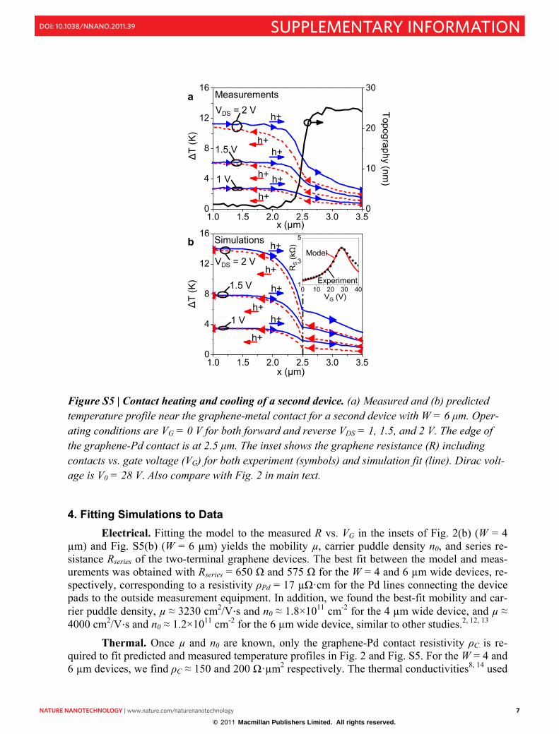
Figure S5 | Contact heating and cooling of a second device. (a) Measured and (b) predicted temperature profile near the graphene-metal contact for a second device with W = 6 μm. Oper-ating conditions are VG = 0 V for both forward and reverse VDS = 1, 1.5, and 2 V. The edge of the graphene-Pd contact is at 2.5 μm. The inset shows the graphene resistance (R) including contacts vs. gate voltage (VG) for both experiment (symbols) and simulation fit (line). Dirac volt-age is V0 = 28 V. Also compare with Fig. 2 in main text.
4. Fitting Simulations to Data
Electrical. Fitting the model to the measured R vs. VG in the insets of Fig. 2(b) (W = 4 µm) and Fig. S5(b) (W = 6 µm) yields the mobility µ, carrier puddle density n0, and series re-sistance Rseries of the two-terminal graphene devices. The best fit between the model and meas-urements was obtained with Rseries = 650 Ω and 575 Ω for the W = 4 and 6 µm wide devices, re-spectively, corresponding to a resistivity ρPd = 17 µΩ·cm for the Pd lines connecting the device pads to the outside measurement equipment. In addition, we found the best-fit mobility and car-rier puddle density, µ ≈ 3230 cm2/V⋅s and n0 ≈ 1.8×1011 cm-2 for the 4 µm wide device, and µ ≈ 4000 cm2/V⋅s and n0 ≈ 1.2×1011 cm-2 for the 6 µm wide device, similar to other studies.2, 12, 13
Thermal. Once µ and n0 are known, only the graphene-Pd contact resistivity ρC is re-quired to fit predicted and measured temperature profiles in Fig. 2 and Fig. S5. For the W = 4 and 6 µm devices, we find ρC ≈ 150 and 200 Ω·µm2 respectively. The thermal conductivities8, 14 used
1.0 1.5 2.0 2.5 3.0 3.50
4
8
12
16
0 10 20 30 401
3
5
1.0 1.5 2.0 2.5 3.0 3.50
4
8
12
16
0
10
20
30a Measurements
VDS = 2 Vh+
h+h+
h+h+
h+
1.5 V
1 V∆T
(K)
Topography (nm)
x (μm)
b
∆T (K
)
x (μm)
Simulations h+
h+
h+
h+
h+
h+
VDS = 2 V
1.5 V
1 V
RS
(kΩ
)VG (V)
Experiment
Model
© 2011 Macmillan Publishers Limited. All rights reserved.

8 nature nanotechnology | www.nature.com/naturenanotechnology
SUPPLEMENTARY INFORMATION doi: 10.1038/nnano.2011.39
8
in the model are listed in Table 1. The thermal conductivity14 of 600 Wm-1K-1 was used for gra-phene with an additional (65/0.34)×0.18 ≈ 35 Wm-1K-1 to simulate lateral heat spreading due to the 65 nm of PMMA on top, although the model is relatively insensitive to this correction.
5. Analysis of 6 µm Wide Device Figure S5 compares measured temperature profiles (a) with predictions (b) for a second-
ary device with W = 6 µm. The analysis of the 6 µm width device is similar to the 4 µm device in the main text and many duplicate details are omitted here. We set VG = 0 V for the predictions and measurements shown in Fig. S5, which corresponds to a hole concentration of p ≈ 2.0× 10¹²
cm-2 as V0 = 28 V. The predicted temperature profiles use the (JH+CC+TE) model, which agrees well with experimental observations.
Figure S6(a) shows how JH, CC, and TE effects change the temperature profile of the 6 µm wide device at the graphene-Pd contact for VDS = 1 V. JH is the dominant effect in the gra-phene itself, as the addition of CC and TE have little change there. However, the addition of CC to JH introduces an additional heat source in the electrode, leading to a more gradual temperature decrease there. CC also introduces the effective current transfer length LT which varies from 520 to 225 nm in the 6 µm wide device, as VG changes from 0 to V0 = 28 V. The addition of the TE effect to the “JH+CC” model introduces electrode heating and cooling with carrier flow, which is evident in the measured temperature profiles. Similar to the 4 µm device (main text), the heating and cooling are better understood when examining the difference between the forward and re-verse biased temperature profiles, as in Fig. S6(b). In the 6 µm wide device the TE effect cools and heats the electrode by ~0.5 K (~30 %). Similar to the 4 µm wide device, ΔTASM is a function of VG, plotted in Fig. S6(c) with experimental measurements at VDS = 1 V.
Figure S6 | Relative contribution of contact effects for a secondary device (W = 6 μm). (a) Simulations showing relative contributions of JH, CC, and TE to the temperature distribution at the graphene-Pd contact at VDS = 1 V and VG = 0 V. Also see Fig 3 of main text. All three com-ponents (TE+CC+JH) are necessary to match the experimental data. (b) Electrode heating and cooling is quantified by taking the difference between temperature under forward and reverse current flow. The maximum temperature difference between the two biases is defined as ΔTASM. (c) Comparison of measured and predicted ΔTASM as a function of VG relative to V0, with JH, CC, and TE contributions to the predicted ΔTASM shown. Also see Fig. 4 of main text.
1.0 1.5 2.0 2.5 3.0 3.50
1
2
3
4
∆T (K
)
a
x (μm)
h+
h+
TE+CC+JH
CC+JH
JH
-30 -20 -10 0 10 20 30-1.0
-0.5
0.0
0.5
1.0
∆T A
SM(K
)
c
TE+CC+JH
Experiment
JH + CC
1.0 1.5 2.0 2.5 3.0 3.50.0
0.2
0.4
0.6
0.8
1.0
x (μm)
b
∆T(j+
) -∆
T(j-)
(K)
∆TASM
TE+CC+JH
TE
JH
j+ - j-
VG - V0 (V)
© 2011 Macmillan Publishers Limited. All rights reserved.

nature nanotechnology | www.nature.com/naturenanotechnology 9
SUPPLEMENTARY INFORMATIONdoi: 10.1038/nnano.2011.39
8
in the model are listed in Table 1. The thermal conductivity14 of 600 Wm-1K-1 was used for gra-phene with an additional (65/0.34)×0.18 ≈ 35 Wm-1K-1 to simulate lateral heat spreading due to the 65 nm of PMMA on top, although the model is relatively insensitive to this correction.
5. Analysis of 6 µm Wide Device Figure S5 compares measured temperature profiles (a) with predictions (b) for a second-
ary device with W = 6 µm. The analysis of the 6 µm width device is similar to the 4 µm device in the main text and many duplicate details are omitted here. We set VG = 0 V for the predictions and measurements shown in Fig. S5, which corresponds to a hole concentration of p ≈ 2.0× 10¹²
cm-2 as V0 = 28 V. The predicted temperature profiles use the (JH+CC+TE) model, which agrees well with experimental observations.
Figure S6(a) shows how JH, CC, and TE effects change the temperature profile of the 6 µm wide device at the graphene-Pd contact for VDS = 1 V. JH is the dominant effect in the gra-phene itself, as the addition of CC and TE have little change there. However, the addition of CC to JH introduces an additional heat source in the electrode, leading to a more gradual temperature decrease there. CC also introduces the effective current transfer length LT which varies from 520 to 225 nm in the 6 µm wide device, as VG changes from 0 to V0 = 28 V. The addition of the TE effect to the “JH+CC” model introduces electrode heating and cooling with carrier flow, which is evident in the measured temperature profiles. Similar to the 4 µm device (main text), the heating and cooling are better understood when examining the difference between the forward and re-verse biased temperature profiles, as in Fig. S6(b). In the 6 µm wide device the TE effect cools and heats the electrode by ~0.5 K (~30 %). Similar to the 4 µm wide device, ΔTASM is a function of VG, plotted in Fig. S6(c) with experimental measurements at VDS = 1 V.
Figure S6 | Relative contribution of contact effects for a secondary device (W = 6 μm). (a) Simulations showing relative contributions of JH, CC, and TE to the temperature distribution at the graphene-Pd contact at VDS = 1 V and VG = 0 V. Also see Fig 3 of main text. All three com-ponents (TE+CC+JH) are necessary to match the experimental data. (b) Electrode heating and cooling is quantified by taking the difference between temperature under forward and reverse current flow. The maximum temperature difference between the two biases is defined as ΔTASM. (c) Comparison of measured and predicted ΔTASM as a function of VG relative to V0, with JH, CC, and TE contributions to the predicted ΔTASM shown. Also see Fig. 4 of main text.
1.0 1.5 2.0 2.5 3.0 3.50
1
2
3
4
∆T (K
)
a
x (μm)
h+
h+
TE+CC+JH
CC+JH
JH
-30 -20 -10 0 10 20 30-1.0
-0.5
0.0
0.5
1.0
∆T A
SM(K
)
c
TE+CC+JH
Experiment
JH + CC
1.0 1.5 2.0 2.5 3.0 3.50.0
0.2
0.4
0.6
0.8
1.0
x (μm)
b
∆T(j+
) -∆
T(j-)
(K)
∆TASM
TE+CC+JH
TE
JH
j+ - j-
VG - V0 (V)
9
6. Extracting the Seebeck Coefficient of Graphene Although in the numerical calculations we use the analytical expression for the Seebeck
coefficient (thermopower) of graphene as in equation (E2), this Seebeck coefficient can also be extracted from direct comparison of the model with our contact temperature measurements. In other words, SG can be obtained from Fig. 4(a) and Fig. S6(c) by fitting the predicted ΔTASM to the measured ΔTASM. The upper and lower limits are found by adjusting ΔTASM until the predicted ΔTASM is out of range of the measurement error bars. The fit of this model is shown in Fig. S7, finding that SG ranges from 27 to 62 µV/K, with the best fit at ~41 µV/K for the 6 µm device and for the 4 µm device SG ranges from 41 to 82 µV/K, with the best fit at ~63 µV/K at VG – V0 = -25 V at 300 K. Across the two devices SG is found to be approximately 52 µV/K, consistent with previous studies.10, 11
Figure S7 | Seebeck coefficient. Extracted Seebeck coefficient at 300 K from the experiment shown with measurements for the 4 µm (a) and 6 µm (b) wide device. The upper and lower limits correspond to fitting the deviation of the measurements at 90% confidence.
7. Movie File: Effect of Back-gate on Contact Heating and Cooling The supplementary movie file details the transition of TE dominated ΔTASM to JH effects
as a function of VG relative to V0 at the graphene-Pd contact by taking the difference between the temperature profile under forward and reverse bias. The movie is similar to Fig. S6(b) with the position of ΔTASM defined by the vertical dashed line. The model parameters are similar to the 6 µm device with ρC = 200 Ω·μm2, μ = 4000 cm2/V⋅s and VDS = 2 V. As VG - V0 approaches zero two events occur: (1) JH hot spot effects become large at the electrode2 and (2) the Seebeck coef-ficient decreases, lowering TE effects.10, 11, 15 After VG - V0 = 0 V the majority carrier switches to electrons which reverses carrier flow, hot spot,2, 16 and the TE effect,10, 11, 15, 17 although the defi-nition of current flow remains the same. As VG – V0 increases, the TE effect increases, hot spot effects decrease, and the curves become similar to their initial states.
-30 -20 -10 0 10 20 30-120
-60
0
60
120
S G(μ
V/K)
a4 μm Device
VG – V0 (V)
Measurements
Upper LimitAverageLower Limit
-30 -20 -10 0 10 20 30-120
-60
0
60
120
S G(μ
V/K)
b6 μm Device
VG – V0 (V)
Measurements
Upper Limit
Lower LimitAverage
© 2011 Macmillan Publishers Limited. All rights reserved.
10 nature nanotechnology | www.nature.com/naturenanotechnology
SUPPLEMENTARY INFORMATION doi: 10.1038/nnano.2011.39
10
Supplementary References:
1. Ferrari, A.C. et al. Raman Spectrum of Graphene and Graphene Layers. Physical Review Letters 97, 187401 (2006).
2. Bae, M.-H., Ong, Z.-Y., Estrada, D. & Pop, E. Imaging, Simulation, and Electrostatic Control of Power Dissipation in Graphene Devices. Nano Letters 10, 4787-4793 (2010).
3. Abdula, D., Ozel, T., Kang, K., Cahill, D.G. & Shim, M. Environment-Induced Effects on the Temperature Dependence of Raman Spectra of Single-Layer Graphene. The Journal of Physical Chemistry C 112, 20131-20134 (2008).
4. Gurrum, S.P., King, W.P., Joshi, Y.K. & Ramakrishna, K. Size Effect on the Thermal Conductivity of Thin Metallic Films Investigated by Scanning Joule Expansion Microscopy. Journal of Heat Transfer 130, 082403-082408 (2008).
5. Majumdar, A. & Varesi, J. Nanoscale Temperature Distributions Measured by Scanning Joule Expansion Microscopy. Journal of Heat Transfer 120, 297-305 (1998).
6. Varesi, J. & Majumdar, A. Scanning Joule expansion microscopy at nanometer scales. Applied Physics Letters 72, 37-39 (1998).
7. Assael, M., Botsios, S., Gialou, K. & Metaxa, I. Thermal Conductivity of Polymethyl Methacrylate (PMMA) and Borosilicate Crown Glass BK7. International Journal of Thermophysics 26, 1595-1605 (2005).
8. Dorgan, V.E., Bae, M.-H. & Pop, E. Mobility and saturation velocity in graphene on SiO2. Applied Physics Letters 97, 082112-082113 (2010).
9. Schroder, D.K. Semiconductor Material and Device Characterization. (Wiley Interscience, 2006).
10. Zuev, Y.M., Chang, W. & Kim, P. Thermoelectric and Magnetothermoelectric Transport Measurements of Graphene. Physical Review Letters 102, 096807 (2009).
11. Checkelsky, J.G. & Ong, N.P. Thermopower and Nernst effect in graphene in a magnetic field. Physical Review B 80, 081413 (2009).
12. Martin, J. et al. Observation of electron-hole puddles in graphene using a scanning single-electron transistor. Nat Phys 4, 144-148 (2008).
13. Kim, S. et al. Realization of a high mobility dual-gated graphene field-effect transistor with Al2O3 dielectric. Applied Physics Letters 94, 062107-062103 (2009).
14. Seol, J.H. et al. Two-Dimensional Phonon Transport in Supported Graphene. Science 328, 213-216 (2010).
15. Wei, P., Bao, W., Pu, Y., Lau, C.N. & Shi, J. Anomalous Thermoelectric Transport of Dirac Particles in Graphene. Physical Review Letters 102, 166808 (2009).
16. Freitag, M., Chiu, H.-Y., Steiner, M., Perebeinos, V. & Avouris, P. Thermal infrared emission from biased graphene. Nat Nano 5, 497-501 (2010).
17. Xu, X., Gabor, N.M., Alden, J.S., van der Zande, A.M. & McEuen, P.L. Photo-Thermoelectric Effect at a Graphene Interface Junction. Nano Letters 10, 562-566 (2009).
© 2011 Macmillan Publishers Limited. All rights reserved.