nanoscale double-gate sram design
TRANSCRIPT

Nanoscale Double-Gate SRAM Design
Erik Eikeland
September 1, 2009


Preface
This theses is submitted in fulfillment of the requirements for the degree
Master of Science at the University of Oslo (UiO). The work has mainly
been carried out at the University Graduate Center (UniK).
i

ii

Dedication
This thesis is dedicated to my mother and father, Ada Eikeland and Hans
Eikeland, and to my beloved girlfriend, Eirin Øvergård, whose constant love
and support helped me through difficult times.
iii

iv

Acknowledgments
I would like to thank Professor Tor Fjeldly who gave me the opportunity to
come to UniK and complete my degree there. Also i would like to thank my
dear, Eirin Øvergård, for her encouragement and patience during my studies.
v

vi

Summary
This work uses an extensive number of simulations to determine the usability
of DG MOSFETs in SRAM circuit design. The simulations have been carried
out in Silvaco ATLAS and MixedMode model and circuit simulation software.
Structures with gate lengths of 50 nm and 20 nm have been tested both
on their own and incorporated into larger circuitry, and these are showing
promising results.
vii

viii

Contents
Preface . . . . . . . . . . . . . . . . . . . . . . . . . . . . . . . . . . i
Dedication . . . . . . . . . . . . . . . . . . . . . . . . . . . . . . . . iii
Acknowledgments . . . . . . . . . . . . . . . . . . . . . . . . . . . . v
Summary . . . . . . . . . . . . . . . . . . . . . . . . . . . . . . . . vii
List of Tables . . . . . . . . . . . . . . . . . . . . . . . . . . . . . . xi
List of Figures . . . . . . . . . . . . . . . . . . . . . . . . . . . . . . xiii
1 Introduction 1
1.1 Background . . . . . . . . . . . . . . . . . . . . . . . . . . . . 1
1.1.1 The transistor . . . . . . . . . . . . . . . . . . . . . . . 2
1.1.2 Memory . . . . . . . . . . . . . . . . . . . . . . . . . . 2
1.1.3 Moore’s Law . . . . . . . . . . . . . . . . . . . . . . . . 3
1.1.4 Integrated Circuit Design . . . . . . . . . . . . . . . . 4
1.1.5 Transistor scaling . . . . . . . . . . . . . . . . . . . . . 4
1.1.6 Design automation . . . . . . . . . . . . . . . . . . . . 5
1.2 Device Simulation . . . . . . . . . . . . . . . . . . . . . . . . . 5
1.3 Circuit Simulation . . . . . . . . . . . . . . . . . . . . . . . . 6
1.4 Objective of Thesis . . . . . . . . . . . . . . . . . . . . . . . . 6
1.5 Outline of Thesis . . . . . . . . . . . . . . . . . . . . . . . . . 6
2 Review of DG MOSFET 9
2.1 Device modeling . . . . . . . . . . . . . . . . . . . . . . . . . . 10
2.2 The simulated structures . . . . . . . . . . . . . . . . . . . . . 12
2.3 Gate work function and the threshold voltage . . . . . . . . . 12
3 The Double-Gate CMOS inverter 19
3.1 Scaling the Supply Voltage . . . . . . . . . . . . . . . . . . . . 20
ix

3.2 Propagation Delay . . . . . . . . . . . . . . . . . . . . . . . . 29
4 Static Random Access Memory(SRAM) 33
4.1 Random Access Memory(RAM) Cells . . . . . . . . . . . . . . 34
4.2 SRAM cell design . . . . . . . . . . . . . . . . . . . . . . . . . 34
4.3 SRAM operation . . . . . . . . . . . . . . . . . . . . . . . . . 35
4.4 SRAM simulations . . . . . . . . . . . . . . . . . . . . . . . . 38
4.4.1 Hold Margin (Retention noise margin) . . . . . . . . . 38
4.4.2 Read Margin(RM) . . . . . . . . . . . . . . . . . . . . 43
4.4.3 Write Margin(WM) . . . . . . . . . . . . . . . . . . . . 47
4.5 DG MOSFET as a Four Terminal Device . . . . . . . . . . . . 54
5 Conclusion 61
6 Future Work 63
6.1 Development of SPICE-type models . . . . . . . . . . . . . . . 63
6.2 MUGFET Z-RAM . . . . . . . . . . . . . . . . . . . . . . . . 64
A SINANO template 65
A.1 Template description . . . . . . . . . . . . . . . . . . . . . . . 65
B Atlas simulation files 69
B.1 Atlas device model . . . . . . . . . . . . . . . . . . . . . . . . 69
B.2 MixedMode circuit file . . . . . . . . . . . . . . . . . . . . . . 72
Bibliography75
x
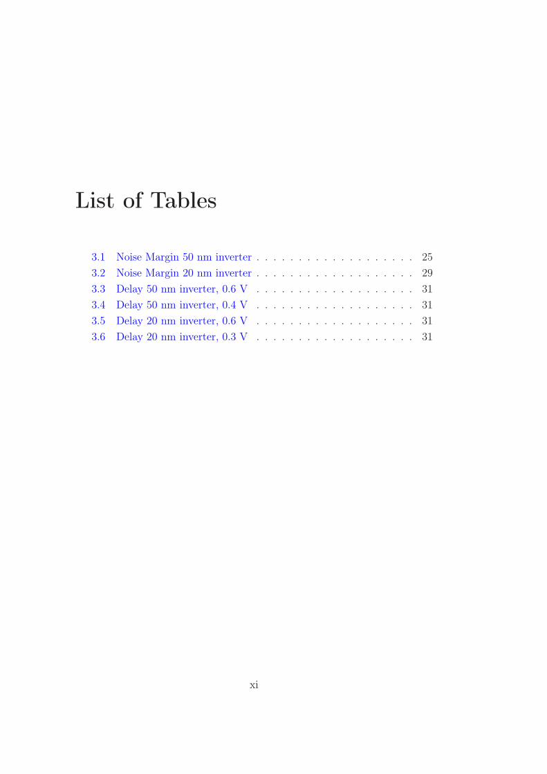
List of Tables
3.1 Noise Margin 50 nm inverter . . . . . . . . . . . . . . . . . . . 25
3.2 Noise Margin 20 nm inverter . . . . . . . . . . . . . . . . . . . 29
3.3 Delay 50 nm inverter, 0.6 V . . . . . . . . . . . . . . . . . . . 31
3.4 Delay 50 nm inverter, 0.4 V . . . . . . . . . . . . . . . . . . . 31
3.5 Delay 20 nm inverter, 0.6 V . . . . . . . . . . . . . . . . . . . 31
3.6 Delay 20 nm inverter, 0.3 V . . . . . . . . . . . . . . . . . . . 31
xi

xii
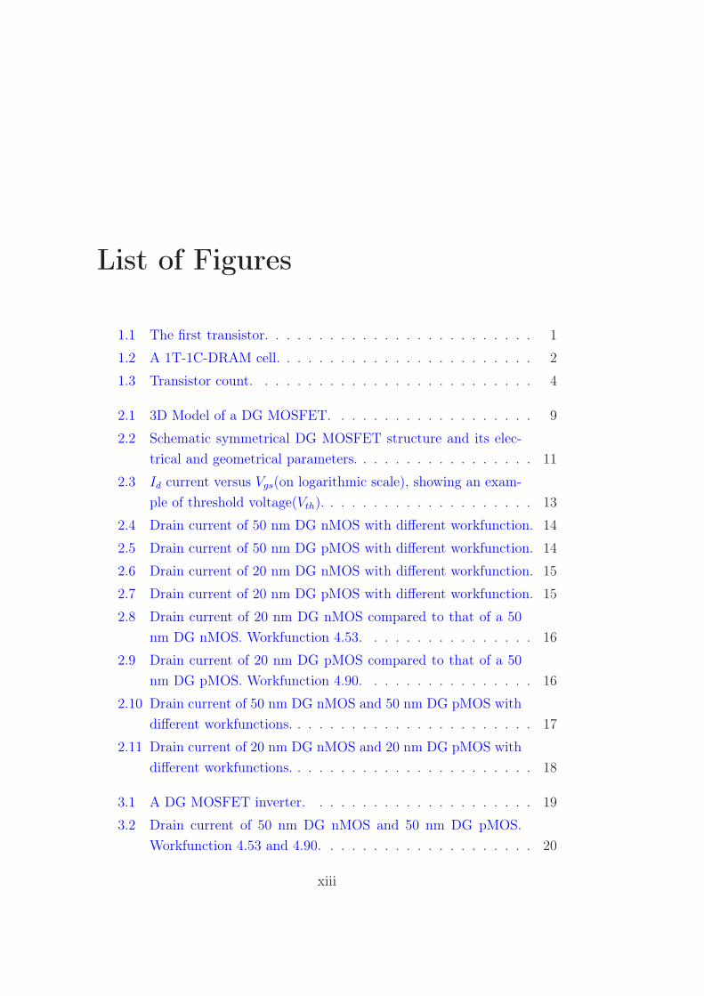
List of Figures
1.1 The first transistor. . . . . . . . . . . . . . . . . . . . . . . . . 1
1.2 A 1T-1C-DRAM cell. . . . . . . . . . . . . . . . . . . . . . . . 2
1.3 Transistor count. . . . . . . . . . . . . . . . . . . . . . . . . . 4
2.1 3D Model of a DG MOSFET. . . . . . . . . . . . . . . . . . . 9
2.2 Schematic symmetrical DG MOSFET structure and its elec-
trical and geometrical parameters. . . . . . . . . . . . . . . . . 11
2.3 Id current versus Vgs(on logarithmic scale), showing an exam-
ple of threshold voltage(Vth). . . . . . . . . . . . . . . . . . . . 13
2.4 Drain current of 50 nm DG nMOS with different workfunction. 14
2.5 Drain current of 50 nm DG pMOS with different workfunction. 14
2.6 Drain current of 20 nm DG nMOS with different workfunction. 15
2.7 Drain current of 20 nm DG pMOS with different workfunction. 15
2.8 Drain current of 20 nm DG nMOS compared to that of a 50
nm DG nMOS. Workfunction 4.53. . . . . . . . . . . . . . . . 16
2.9 Drain current of 20 nm DG pMOS compared to that of a 50
nm DG pMOS. Workfunction 4.90. . . . . . . . . . . . . . . . 16
2.10 Drain current of 50 nm DG nMOS and 50 nm DG pMOS with
different workfunctions. . . . . . . . . . . . . . . . . . . . . . . 17
2.11 Drain current of 20 nm DG nMOS and 20 nm DG pMOS with
different workfunctions. . . . . . . . . . . . . . . . . . . . . . . 18
3.1 A DG MOSFET inverter. . . . . . . . . . . . . . . . . . . . . 19
3.2 Drain current of 50 nm DG nMOS and 50 nm DG pMOS.
Workfunction 4.53 and 4.90. . . . . . . . . . . . . . . . . . . . 20
xiii
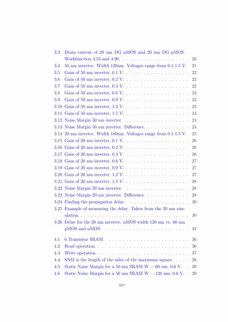
3.3 Drain current of 20 nm DG nMOS and 20 nm DG pMOS.
Workfunction 4.53 and 4.90. . . . . . . . . . . . . . . . . . . . 20
3.4 50 nm inverter. Width 120nm. Voltages range from 0.1-1.5 V. 21
3.5 Gain of 50 nm inverter, 0.1 V. . . . . . . . . . . . . . . . . . . 22
3.6 Gain of 50 nm inverter, 0.2 V. . . . . . . . . . . . . . . . . . . 22
3.7 Gain of 50 nm inverter, 0.3 V. . . . . . . . . . . . . . . . . . . 22
3.8 Gain of 50 nm inverter, 0.6 V. . . . . . . . . . . . . . . . . . . 23
3.9 Gain of 50 nm inverter, 0.9 V. . . . . . . . . . . . . . . . . . . 23
3.10 Gain of 50 nm inverter, 1.2 V. . . . . . . . . . . . . . . . . . . 23
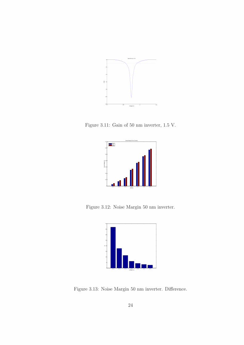
3.11 Gain of 50 nm inverter, 1.5 V. . . . . . . . . . . . . . . . . . . 24
3.12 Noise Margin 50 nm inverter. . . . . . . . . . . . . . . . . . . 24
3.13 Noise Margin 50 nm inverter. Difference. . . . . . . . . . . . . 24
3.14 20 nm inverter. Width 180nm. Voltages range from 0.1-1.5 V. 25
3.15 Gain of 20 nm inverter, 0.1 V. . . . . . . . . . . . . . . . . . . 26
3.16 Gain of 20 nm inverter, 0.2 V. . . . . . . . . . . . . . . . . . . 26
3.17 Gain of 20 nm inverter, 0.3 V. . . . . . . . . . . . . . . . . . . 26
3.18 Gain of 20 nm inverter, 0.6 V. . . . . . . . . . . . . . . . . . . 27
3.19 Gain of 20 nm inverter, 0.9 V. . . . . . . . . . . . . . . . . . . 27
3.20 Gain of 20 nm inverter, 1.2 V. . . . . . . . . . . . . . . . . . . 27
3.21 Gain of 20 nm inverter, 1.5 V. . . . . . . . . . . . . . . . . . . 28
3.22 Noise Margin 20 nm inverter. . . . . . . . . . . . . . . . . . . 28
3.23 Noise Margin 20 nm inverter. Difference. . . . . . . . . . . . . 28
3.24 Finding the propagation delay. . . . . . . . . . . . . . . . . . . 30
3.25 Example of measuring the delay. Taken from the 20 nm sim-
ulation . . . . . . . . . . . . . . . . . . . . . . . . . . . . . . . 30
3.26 Delay for the 20 nm inverter. nMOS width 120 nm vs. 60 nm
pMOS and nMOS. . . . . . . . . . . . . . . . . . . . . . . . . 32
4.1 6 Transistor SRAM. . . . . . . . . . . . . . . . . . . . . . . . 36
4.2 Read operation. . . . . . . . . . . . . . . . . . . . . . . . . . . 36
4.3 Write operation. . . . . . . . . . . . . . . . . . . . . . . . . . . 37
4.4 SNM is the length of the sides of the maximum square. . . . . 38
4.5 Static Noise Margin for a 50 nm SRAM W = 60 nm, 0.6 V. . 39
4.6 Static Noise Margin for a 50 nm SRAM W = 120 nm, 0.6 V. . 39
xiv

4.7 Static Noise Margin for a 50 nm SRAM W = 60 nm, 0.3 V. . 40
4.8 Static Noise Margin for a 50 nm SRAM W = 120 nm, 0.3 V. . 40
4.9 Static Noise Margin for a 20 nm SRAM W = 60 nm, 0.6 V. . 40
4.10 Static Noise Margin for a 20 nm SRAM W = 120 nm, 0.6 V. . 41
4.11 Static Noise Margin for a 20 nm SRAM W = 180 nm, 0.6 V. . 41
4.12 Static Noise Margin for a 20 nm SRAM W = 60 nm, 0.3 V. . 41
4.13 Static Noise Margin for a 20 nm SRAM W = 120 nm, 0.3 V. . 42
4.14 Static Noise Margin for a 20 nm SRAM W = 180 nm, 0.3 V. . 42
4.15 Read Noise Margin for a 50 nm SRAM W = 60 nm, 0.6 V. . . 43
4.16 Read Noise Margin for a 50 nm SRAM W = 120 nm, 0.6 V. . 44
4.17 Read Noise Margin for a 50 nm SRAM W = 60 nm, 0.3 V. . . 44
4.18 Read Noise Margin for a 50 nm SRAM W = 120 nm, 0.3 V. . 45
4.19 Read Noise Margin for a 20 nm SRAM W = 60 nm, 0.6 V. . . 45
4.20 Read Noise Margin for a 20 nm SRAM W = 120 nm, 0.6 V. . 45
4.21 Read Noise Margin for a 20 nm SRAM W = 60 nm, 0.3 V. . . 46
4.22 Read Noise Margin for a 20 nm SRAM W = 120 nm, 0.3 V. . 46
4.23 Write Noise Margin for a 50 nm SRAM W = 60 nm, 0.6 V. . . 47
4.24 Write Noise Margin for a 50 nm SRAM W = 120 nm, 0.6 V. . 47
4.25 Write Noise Margin for a 50 nm SRAM W = 60 nm, 0.3 V. . . 48
4.26 Write Noise Margin for a 50 nm SRAM W = 120 nm, 0.3 V. . 48
4.27 Write Noise Margin for a 20 nm SRAM W = 60 nm, 0.6 V. . . 48
4.28 Write Noise Margin for a 20 nm SRAM W = 120 nm, 0.6 V. . 49
4.29 Write Noise Margin for a 20 nm SRAM W = 180 nm, 0.6 V. . 49
4.30 Write Noise Margin for a 20 nm SRAM W = 60 nm, 0.3 V. . . 49
4.31 Write Noise Margin for a 20 nm SRAM W = 120 nm, 0.3 V. . 50
4.32 Write Noise Margin for a 20 nm SRAM W = 180 nm, 0.3 V. . 50
4.33 Switching delay during write. . . . . . . . . . . . . . . . . . . 51
4.34 Noise Margin for a 50 nm SRAM. Comparing W = 60 nm and
W = 120 nm, 0.6 V. . . . . . . . . . . . . . . . . . . . . . . . 52
4.35 Noise Margin for a 50 nm SRAM. Comparing W = 60 nm and
W = 120 nm, 0.3 V. . . . . . . . . . . . . . . . . . . . . . . . 52
4.36 Noise Margin for a 20 nm SRAM. Comparing W = 60 nm, W
= 120 nm and 180 nm, 0.6 V. . . . . . . . . . . . . . . . . . . 53
xv
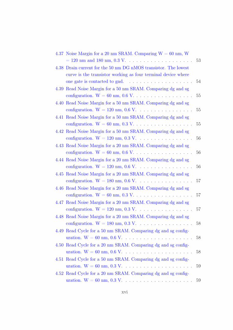
4.37 Noise Margin for a 20 nm SRAM. Comparing W = 60 nm, W
= 120 nm and 180 nm, 0.3 V. . . . . . . . . . . . . . . . . . . 53
4.38 Drain current for the 50 nm DG nMOS transistor. The lowest
curve is the transistor working as four terminal device where
one gate is contacted to gnd. . . . . . . . . . . . . . . . . . . 54
4.39 Read Noise Margin for a 50 nm SRAM. Comparing dg and sg
configuration. W = 60 nm, 0.6 V. . . . . . . . . . . . . . . . . 55
4.40 Read Noise Margin for a 50 nm SRAM. Comparing dg and sg
configuration. W = 120 nm, 0.6 V. . . . . . . . . . . . . . . . 55
4.41 Read Noise Margin for a 50 nm SRAM. Comparing dg and sg
configuration. W = 60 nm, 0.3 V. . . . . . . . . . . . . . . . . 55
4.42 Read Noise Margin for a 50 nm SRAM. Comparing dg and sg
configuration. W = 120 nm, 0.3 V. . . . . . . . . . . . . . . . 56
4.43 Read Noise Margin for a 20 nm SRAM. Comparing dg and sg
configuration. W = 60 nm, 0.6 V. . . . . . . . . . . . . . . . . 56
4.44 Read Noise Margin for a 20 nm SRAM. Comparing dg and sg
configuration. W = 120 nm, 0.6 V. . . . . . . . . . . . . . . . 56
4.45 Read Noise Margin for a 20 nm SRAM. Comparing dg and sg
configuration. W = 180 nm, 0.6 V. . . . . . . . . . . . . . . . 57
4.46 Read Noise Margin for a 20 nm SRAM. Comparing dg and sg
configuration. W = 60 nm, 0.3 V. . . . . . . . . . . . . . . . . 57
4.47 Read Noise Margin for a 20 nm SRAM. Comparing dg and sg
configuration. W = 120 nm, 0.3 V. . . . . . . . . . . . . . . . 57
4.48 Read Noise Margin for a 20 nm SRAM. Comparing dg and sg
configuration. W = 180 nm, 0.3 V. . . . . . . . . . . . . . . . 58
4.49 Read Cycle for a 50 nm SRAM. Comparing dg and sg config-
uration. W = 60 nm, 0.6 V. . . . . . . . . . . . . . . . . . . . 58
4.50 Read Cycle for a 20 nm SRAM. Comparing dg and sg config-
uration. W = 60 nm, 0.6 V. . . . . . . . . . . . . . . . . . . . 58
4.51 Read Cycle for a 50 nm SRAM. Comparing dg and sg config-
uration. W = 60 nm, 0.3 V. . . . . . . . . . . . . . . . . . . . 59
4.52 Read Cycle for a 20 nm SRAM. Comparing dg and sg config-
uration. W = 60 nm, 0.3 V. . . . . . . . . . . . . . . . . . . . 59
xvi

4.53 Read Noise Margin for a 50 nm SRAM. Comparing dg and sg
configuration. W = 60 nm . . . . . . . . . . . . . . . . . . . . 59
4.54 Read Noise Margin for a 20 nm SRAM. Comparing dg and sg
configuration. W = 60 nm . . . . . . . . . . . . . . . . . . . . 60
A.1 Source to drain cuts of doping profile at the silicon/oxide
boundary(blue) and at the center symmetry line. . . . . . . . 66
A.2 Source contact potential profile for template and ideal device. 67
A.3 Source to drain potential profile at the center symmetry line
for template and ideal device. . . . . . . . . . . . . . . . . . . 68
xvii

xviii

Chapter 1
Introduction
1.1 Background
During the first half of the 20th century, electronic circuits used large, ex-
pensive, power-hungry, and unreliable vacuum tubes. In 1947, John Bardeen
and Walter Brattain built the first functioning point contact transistor at
Bell Laboratories. It was nearly classified as a military secret, but Bell Lab-
oratories publicly announced the device in the following year.
Figure 1.1: The first transistor.
1

1.1.1 The transistor
We have called it the Transistor, T-R-A-N-S-I-S-T-O-R, because
it is a resistor or semiconductor device which can amplify electri-
cal signals as they are transferred through it from input to output
terminals. It is, if you will, the electrical equivalent of a vacuum
tube amplifier. But there the similarity ceases. It has no vacuum,
no filament, no glass tube. It is composed entirely of cold, solid
substances.
These are the words Ralph Bown used when he announced the new inven-
tion on June 30, 1948, at a press conference held in the Bell Laboratories
headquarters. The transistor is the fundamental building block of modern
electronic devices, and is used in radio, telephone, computer and other elec-
tronic systems. The transistor is often cited as being one of the greatest
achievements in the 20th century, and some consider it one of the most im-
portant technological breakthroughs in human history. The invention of the
transistor earned the Nobel Prize in Physics in 1956 for Bardeen, Brattain
and their co-worker William Shockley.
1.1.2 Memory
Figure 1.2: A 1T-1C-DRAM cell.
2

A memory unit is a device to which binary information is transferred for
storage and which information is available when needed for processing. There
are two main types of memories that are used in digital systems: Random-
Access Memory(RAM) and Read-Only Memory (ROM). Examples of RAM
are Dynamic Random Access Memory (DRAM) 1.2, a type of memory which
needs to be refreshed periodically or else looses its stored data, and Static
Random Access Memory (SRAM) which does not have a refresh requirement
but is still, like the DRAM, volatile in the conventional sense that data is
eventually lost when the memory is not powered.
ROM memory is a non-volatile memory, it retains the stored information
even when not powered. Early ROM memory could not be modified (at least
not very quickly or easily) and was mainly used to distribute firmware. How-
ever, more modern types such as Erasable Programmable Read-Only Memory
(EPROM) and flash1 Electrically Erasable Programmable Read-Only Mem-
ory (EEPROM) can be erased and re-programmed multiple times, they are
still described as ROM because the reprogramming process is generally infre-
quent, comparatively slow, and often does not permit random access writes
to individual memory locations.
1.1.3 Moore’s Law
In 1965, Gordon Moore, then a Director of Research and Development Lab-
oratories, at Fairchild Semiconductor, released a paper[1] where he described
an important trend in computer hardware. This was later to become the
renowned Moore’s Law. Moore’s Law says that the number of transistors
that can be inexpensively placed on an integrated circuit is increasing expo-
nentially with time, doubling approximately every two years 1.3. This trend
continues even today and is not expected to stop for another decade. Al-
most every measure of the capabilities of digital electronic devices is linked
to Moore’s Law, for example processing speed and memory capacity. All of
1According to Toshiba, the name flash was suggested by Dr. Fujio Masuoka’s(the
inventor of flash memory) colleague, Mr. Shoji Ariizumi, because the erasure process of
the memory contents reminded him of a flash of a camera. Dr. Masuoka presented the
invention at the IEEE 1984 International Electron Devices Meeting (IEDM) held in San
Francisco, California.
3
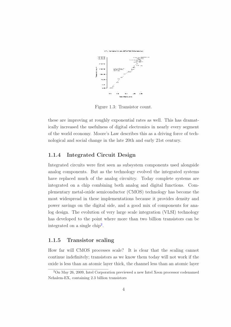
Figure 1.3: Transistor count.
these are improving at roughly exponential rates as well. This has dramat-
ically increased the usefulness of digital electronics in nearly every segment
of the world economy. Moore’s Law describes this as a driving force of tech-
nological and social change in the late 20th and early 21st century.
1.1.4 Integrated Circuit Design
Integrated circuits were first seen as subsystem components used alongside
analog components. But as the technology evolved the integrated systems
have replaced much of the analog circuitry. Today complete systems are
integrated on a chip combining both analog and digital functions. Com-
plementary metal-oxide semiconductor (CMOS) technology has become the
most widespread in these implementations because it provides density and
power savings on the digital side, and a good mix of components for ana-
log design. The evolution of very large scale integration (VLSI) technology
has developed to the point where more than two billion transistors can be
integrated on a single chip2.
1.1.5 Transistor scaling
How far will CMOS processes scale? It is clear that the scaling cannot
continue indefinitely; transistors as we know them today will not work if the
oxide is less than an atomic layer thick, the channel less than an atomic layer
2On May 26, 2009, Intel Corporation previewed a new Intel Xeon processor codenamed
Nehalem-EX, containing 2.3 billion transistors
4

long, or the charge in the channel less than that of one electron. Numerous
papers have been written forecasting the end of silicon scaling. For example,
in 1972, the limit was placed at the 0.25µ generation because of tunneling
and fluctuations in dopant distributions[2]; at this generation, chips were
predicted to operate at 10-30 MHz. In 1999, IBM predicted that scaling
would nearly grind to a halt beyond the 100 nm generation in 2004[3].
1.1.6 Design automation
To keep pace with this rapid change, electronics products have to be designed
extremely quickly. Digital design has become very dependent on computer-
aided design (CAD) - also known as design automation(DA) or electronic
design automation (EDA). The CAD tools allow two task to be performed:
synthesis, in other words the translation of a specification into an actual im-
plementation of the design; and simulation, in which the specification or the
detailed implementation can be exercised in order to verify correct operation.
1.2 Device Simulation
Device simulation tools simulate the electrical characteristics of semiconduc-
tor devices, as a response to external electrical, thermal or optical boundary
conditions imposed on the structure. By ‘building‘ the device in a process
simulators, the simulator can predict the structures that result from a speci-
fied process sequences (such as diffusion and ion implantation), based on the
physics and chemistry of the semiconductor processes. CAD tools apply nu-
merical derivations based on complex equations, such as partial differential
equations, to predict the behavior of the device. Silvaco ATLAS, one of the
TCAD tools and the one used in this thesis, provides a physics-based plat-
form to analyze DC, AC, and time domain responses for all semiconductor
based technologies in 2 and 3 dimensions.
5

1.3 Circuit Simulation
SPICE 3 is a general-purpose circuit simulation program for nonlinear dc,
nonlinear transient, and linear ac analyses. The program was developed at
the University of California, Berkeley. Silvaco MixedMode is a circuit simula-
tor that includes physically-based devices in addition to compact analytical
models. Physically-based devices are used when accurate compact models
do not exist, or when devices that play a critical role must be simulated
with very high accuracy. The physically-based devices are placed along side
a circuit description that conforms to SPICE net list format. The circuit
description used in this thesis are found in Appendix B.
1.4 Objective of Thesis
The main objective of this thesis is to investigate the DG MOSFET usabil-
ity when it comes to SRAM design. This is done by subjecting the DG
MOSFETs to a great number of simulations which test many aspects of
its performance characteristics. The future of CMOS design, when scaling
is concerned, is challenging but also exciting, and to explore and simulate
novel transistor designs is a important part of continuing the technology de-
velopment. All simulations use a physically-based two-dimensional structure
of the DG MOSFET build in ATLAS. This is den given a third dimension
(width) when used in the MixedMode circuit simulation.
1.5 Outline of Thesis
Chapter 2, gives an introduction to the device considered in this work. Device
modeling for DG MOSFET devices are presented and simulations are done in
order to determine the gate work function’s role in setting the DG MOSFETs
threshold voltage (Vth).
In Chapter 3, the CMOS inverter, based on DG MOSFETs, is tested to
investigate important operating parameters. Simulation results are given and
discussed.3Simulation Program with Integrated Circuit Emphasis
6

In Chapter 4, the SRAM cell is presented. This chapter is the main part
of this thesis and gives an overview of the operation of SRAM and different
design schemes of SRAM cells. Numerous simulations are done. The SRAM
cells ability to hold the bit information is measured, the write ability and the
read ability are checked and the results analyzed and presented.
Chapter 6 contains the conclusion and Chapter 7 discusses possible future
work.
7

8
Chapter 2
Review of DG MOSFET
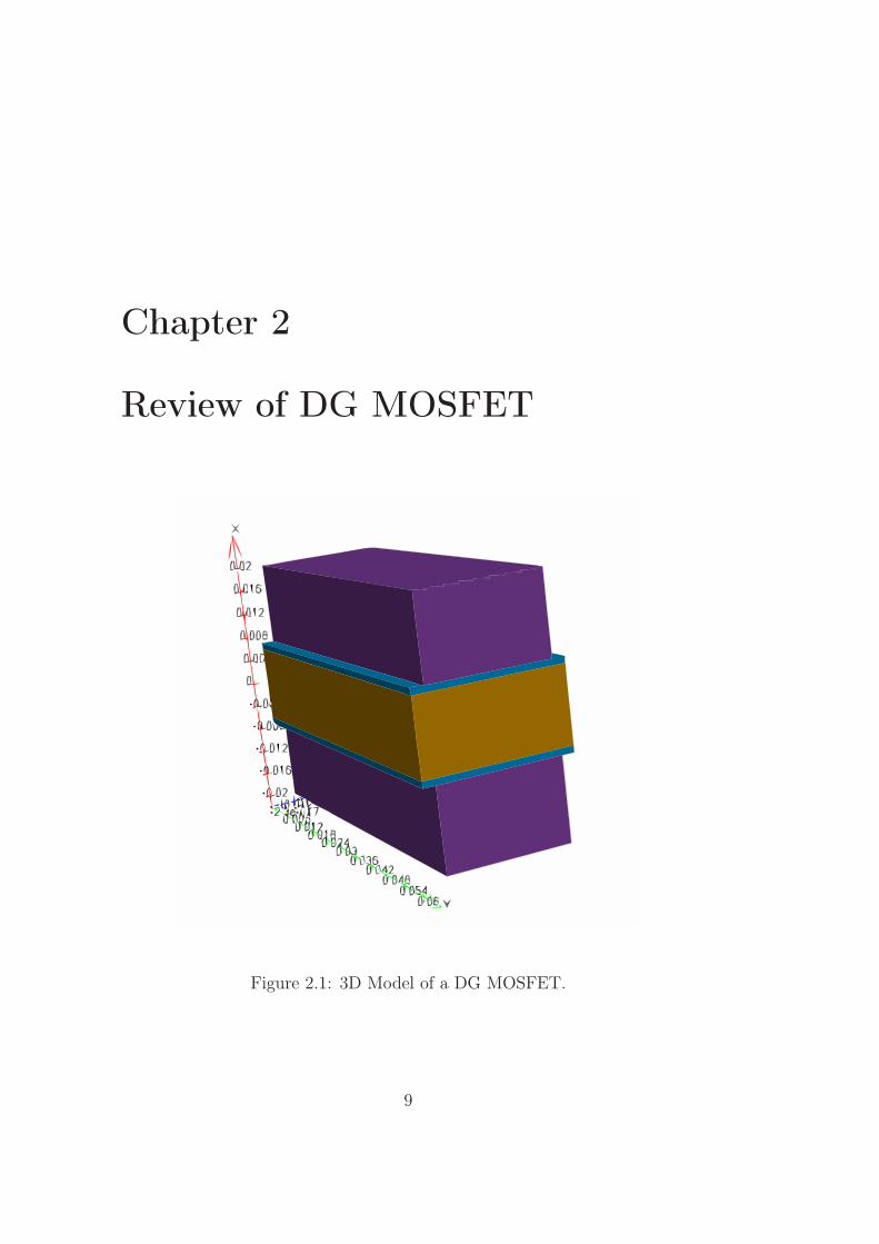
Figure 2.1: 3D Model of a DG MOSFET.
9

It is expected that the current CMOS technology, conventional planer
bulk transistor, will be difficult to scale effectively, even with the utilization
of high-k gate dielectrics1, metal electrodes, strained silicon2 and other new
materials being considered[4]. Multi Gate Field Effect Transistor(MUGFET)
is thought to be the leading new transistor technology which will take over
as the leading workhorse in digital electronics. According to the projection
of the 2008 International Technology Roadmap for Semiconductor, devices
with gate lengths down to 10 nm can be expected in 2019[5]. The Double-
Gate MOSFET (DGMOSFET) structure minimizes short-channel effects in
order to allow a more aggressive device downscaling[6], and numerical simu-
lations have shown that it can be scalable down to 10 nm gate length[7][8].In
ultimately scaled technology, CMOS circuit leakage power would be signifi-
cantly reduced by DG devices. Considering power and performance trade-off
in circuit design, the DG inverter could offer lower leakage power or faster
performance due to near-ideal slope factor (S ) and lower Drain-Induced Bar-
rier Lowering(DIBL). DG device will be much more scalable. This chapter
gives a presentation of the DG MOSFET design which is the basis of the DG
MOSFETs used in the simulations in this thesis. It also gives an introduction
to DG MOSFET modeling.
2.1 Device modeling
In order to calculate currents and capacitances in the DG MOSFET, the
device electrostatics must be modeled. All modeling attempts are based on
the 2D Poisson’s equation as the DG MOSFET is dominated by 2D electrical
fields. The electrostatic potential, ϕ(x, y) in the semiconductor body of the
DG MOSFET is given by:
∂2ϕ(x, y)
∂x2+
∂2ϕ(x, y)
∂y2=
q
εSi
(Na + n) , (2.1)
1High-k stands for high dielectric constant. This means one can increase the thickness
of the insulator layer and still have the same gate control.2Silicon atoms are stretched beyond their normal inter atomic distance, meaning elec-
trons move more freely.
10

Figure 2.2: Schematic symmetrical DG MOSFET structure and its electrical
and geometrical parameters.
where Na is the acceptor doping density in the silicon body (n-channel de-
vice), n is the mobile charge density and εSi is the permittivity of silicon.
The 2D Poisson’s equation can in accordance with the superposition prin-
ciple, be separated into a simplified Poisson equation and a Laplace equation
for the mobile charge contribution and the inter-electrode coupling, respec-
tively. I.e. for the DG device
∂2ϕ1
∂x2+
∂2ϕ1
∂y2=
qn
εsi
(2.2)
∂2ϕ2
∂x2+
∂2ϕ2
∂y2= 0 (2.3)
where ϕ1 can be related to the inversion charge, and ϕ2 to the inter-
electrode coupling. The total potential is then given as the sum of these two
contributions ϕ = ϕ1 + ϕ2.
Many technique have been have been used to make compact models of
DG Devices. One of them utilizes a mathematical technique called confor-
mal mapping. Conformal mapping was introduced as a technique to calculate
the two-dimensional effects of short-channel devices. The first example of the
application of this technique was shown in by Klös et al. in [9]. They used
conformal mapping to map the fields of a semi-infinite slab of silicon into a
complex plane with analytical solutions. The boundary conditions of this 2D
solution included the field from the depletion charge and most short-channel
effects became intrinsic to the model. This bulk MOSFET model was later
11

refined by Østhaug et al. [10], who simplified the integrals associated with
the conformal mapping procedure. The model was also verified against ex-
perimental results from sub-100nm single gate devices with good agreement.
Based on the above work Kolberg et al. applied the conformal mapping pro-
cedure to the double gate MOSFET [11][12][13][14], and found an analytical
solution to the inter-electrode electrostatics of the device. These compact
models which are further being developed by Fjeldly et al. could be a basis
for models applicable for circuit simulation.
2.2 The simulated structures
The DG MOSFETs which are examined in this work are based on a physical
device template described in Appendix A. The channel lengths of the devices
are L = 50 nm and L = 20 nm, and nitride oxide thickness that is set at
tox = 1.6 nm and tox = 1 nm respectively, and a body of lightly doped sili-
con that is tSi = 12nm high. Nitrated oxide and silicon have permittivities
of ǫox = 7 and ǫSi= 11.8. The source/drain contact surfaces are defined to
be sharp boundaries where on the body side of the nMOS DG MOSFET
we have a acceptor concentration of NS = 1· 1015cm−3 corresponding to p−
type silicon and on source and drain sides we have an donor concentration
of NS = 1·1020cm−3 corresponding to that of n+ type silicon. For the pMOS
DG MOSFET we have a acceptor concentration of NS = 1·1015cm−3 corre-
sponding to n− type silicon and on source and drain sides we have an donor
concentration of NS = 1·1020cm−3 corresponding to that of p+ type silicon.
2.3 Gate work function and the threshold volt-
age
The energy difference between the vacuum level and highest occupied elec-
tronic state is called the work function(φm). The φm represents the energy
required to remove an electron out to the free vacuum level. Adjusting the
gate work function changes the threshold voltage(Vth) 2.3 of the DG MOS-
FET device. Three different sets of φm were tested and compared. φm =
12

4.17 eV for nMOS and φm = 5.25 eV for pMOS (band-edge, BE), φm = 4.71
eV for nMOS and φm = 4.71 eV for pMOS (mid gap, MG), φm typically for
polysilicon gate material, and φm = 4.53 eV for nMOS and φm = 4.90 eV for
pMOS, φm for molybdenum gate material[15]. Drain voltage VD was held at
0.1 V, while the gate voltage VG was increased.
Figure 2.3: Id current versus Vgs(on logarithmic scale), showing an example
of threshold voltage(Vth).
13

−1 −0.5 0 0.5 1 1.510
−18
10−16
10−14
10−12
10−10
10−8
10−6
10−4
10−2
100
Gate Voltage(V)
Dra
in C
urre
nt (
I)
Drain Current
4.534.174.71
Figure 2.4: Drain current of 50 nm DG nMOS with different workfunction.
−1.5 −1 −0.5 0 0.5 110
−18
10−16
10−14
10−12
10−10
10−8
10−6
10−4
10−2
Gate Voltage(V)
Dra
in C
urre
nt(I
)
Drain Current
4.715.254.90
Figure 2.5: Drain current of 50 nm DG pMOS with different workfunction.
14

−1 −0.5 0 0.5 1 1.510
−14
10−12
10−10
10−8
10−6
10−4
10−2
100
Gate Voltage (V)
Dra
in C
urre
nt (
I)
Drain Current
4.714.534.17
Figure 2.6: Drain current of 20 nm DG nMOS with different workfunction.
−1.5 −1 −0.5 0 0.5 1
−100
−10−2
−10−4
−10−6
−10−8
−10−10
−10−12
−10−14
Gate Voltage (V)
Dra
in C
urre
nt (
I)
Drain Current
4.715.254.90
Figure 2.7: Drain current of 20 nm DG pMOS with different workfunction.
15

−1 −0.5 0 0.5 1 1.510
−16
10−14
10−12
10−10
10−8
10−6
10−4
10−2
100
Gate Voltage (V)
Dra
in C
urre
nt (
I)
Drain Current
20 nm nMos50nm nMos
Figure 2.8: Drain current of 20 nm DG nMOS compared to that of a 50 nm
DG nMOS. Workfunction 4.53.
−1.5 −1 −0.5 0 0.510
−16
10−14
10−12
10−10
10−8
10−6
10−4
10−2
100
Gate Voltage (V)
Dra
in C
urre
nt (
I)
Drain Current
50 nm pMOS20 nm pMOS
Figure 2.9: Drain current of 20 nm DG pMOS compared to that of a 50 nm
DG pMOS. Workfunction 4.90.
16

Looking at the results from the simulations, the φm chosen for the SRAM
design was that of φm = 4.53 eV for nMOS and φm = 4.90 eV for pMOS. A
high Vth means that the drive current of these devices is small making the
write operation of the SRAM (both accidental and intentional) more difficult.
On the other hand a low Vth means the write operation goes faster and easier
but is more sensible to noise. One should also notice the slope factor in the
simulations. The slope factor S, measures how much VGS has to be reduced
for the drain current to drop by a factor of 10. S is expressed in mV/decade
and is defined:
S = nkBT
qln(10) (2.4)
For an ideal transistor with the sharpest possible roll off, n3 = 1 evaluates
to 60 mV/decade at room temperature, which means that the sub threshold
current drops by a factor of 10 for a reduction in VGS of 60 mV. Our simu-
lations gives us a slope factor of S = 85 mV/decade for the 20 nm structure
and near ideal S = 63 mV/decade for the 50 nm structure.
−1.5 −1 −0.5 0 0.5 1 1.510
−18
10−16
10−14
10−12
10−10
10−8
10−6
10−4
10−2
100
Gate Voltage (V)
Dra
in C
urre
nt (
I)
Drain Current
4.71 pMOS4.90 pMOS5.25 pMOS4.17 nMOS4.53 nMOS4.71 nMOS
Figure 2.10: Drain current of 50 nm DG nMOS and 50 nm DG pMOS with
different workfunctions.
3The value of n is determined by the intrinsic device topology and structure
17

−1.5 −1 −0.5 0 0.5 1 1.510
−14
10−12
10−10
10−8
10−6
10−4
10−2
100
Gate Voltage (V)
Dra
in C
urre
nt (
I)
Drain Current
4.71 pMOS5.25 pMOS4.90 pMOS4.53 nMOS4.71 nMOS4.17 nMOS
Figure 2.11: Drain current of 20 nm DG nMOS and 20 nm DG pMOS with
different workfunctions.
18

Chapter 3
The Double-Gate CMOS inverter
Figure 3.1: A DG MOSFET inverter.
The inverter 3.1 is truly the nucleus of all digital designs. Once its oper-
ation and properties are clearly understood, designing more intricate struc-
tures such as NAND gates, adders, multipliers, memory and microprocessors
19
is greatly simplified. The electrical behavior of these complex circuits can
be almost completely derived by extrapolating the results obtained for in-
verters. The analysis of inverters can be extended to explain the behavior of
more complex gates such as NAND, NOR, or XOR, which in turn form the
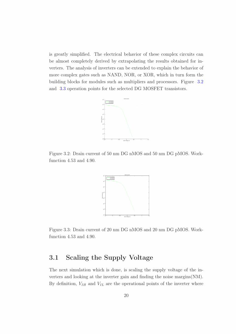
building blocks for modules such as multipliers and processors. Figure 3.2
and 3.3 operation points for the selected DG MOSFET transistors.
−1.5 −1 −0.5 0 0.5 1 1.510
−16
10−14
10−12
10−10
10−8
10−6
10−4
10−2
100
Gate Voltage (V)
Dra
in C
urre
nt (
I)
Drain Current
4.90 pMOS4.53 nMOS
Figure 3.2: Drain current of 50 nm DG nMOS and 50 nm DG pMOS. Work-
function 4.53 and 4.90.
−1.5 −1 −0.5 0 0.5 1 1.510
−14
10−12
10−10
10−8
10−6
10−4
10−2
100
Gate Voltage (V)
Dra
in C
urre
nt (
I)
Drain Current
4.90 pMOS4.53 nMOS
Figure 3.3: Drain current of 20 nm DG nMOS and 20 nm DG pMOS. Work-
function 4.53 and 4.90.
3.1 Scaling the Supply Voltage
The next simulation which is done, is scaling the supply voltage of the in-
verters and looking at the inverter gain and finding the noise margins(NM).
By definition, VIH and VIL are the operational points of the inverter where
20
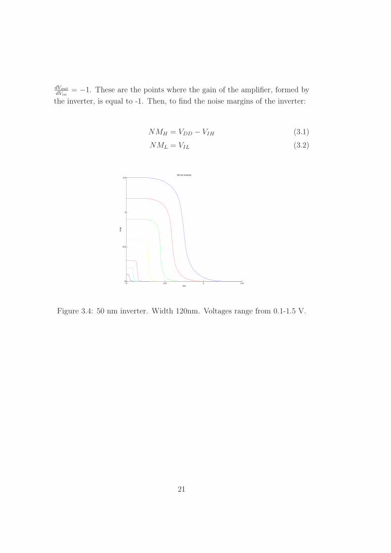
dVout
dVin= −1. These are the points where the gain of the amplifier, formed by
the inverter, is equal to -1. Then, to find the noise margins of the inverter:
NMH = VDD − VIH (3.1)
NML = VIL (3.2)
0 0.5 1 1.50
0.5
1
1.5
Vin
Vou
t
50 nm inverter
Figure 3.4: 50 nm inverter. Width 120nm. Voltages range from 0.1-1.5 V.
21

0 0.01 0.02 0.03 0.04 0.05 0.06 0.07 0.08 0.09 0.1−4.5
−4
−3.5
−3
−2.5
−2
−1.5
−1
−0.5
0
Voltage (V)
Gai
n
Gain 50nm, 0.1 V
Figure 3.5: Gain of 50 nm inverter, 0.1 V.
0 0.02 0.04 0.06 0.08 0.1 0.12 0.14 0.16 0.18 0.2−12
−10
−8
−6
−4
−2
0
Voltage (V)
Gai
n
Gain 50 nm, 0.2 V
Figure 3.6: Gain of 50 nm inverter, 0.2 V.
0 0.05 0.1 0.15 0.2 0.25 0.3−18
−16
−14
−12
−10
−8
−6
−4
−2
0
Voltage (V)
Gai
n
Gain 50 nm, 0.3V
Figure 3.7: Gain of 50 nm inverter, 0.3 V.
22

0 0.1 0.2 0.3 0.4 0.5 0.6−20
−18
−16
−14
−12
−10
−8
−6
−4
−2
0
Voltage (V)
Gai
n
Gain 50 nm, 0.6 V
Figure 3.8: Gain of 50 nm inverter, 0.6 V.
0 0.1 0.2 0.3 0.4 0.5 0.6 0.7 0.8 0.9−16
−14
−12
−10
−8
−6
−4
−2
0
Voltage (V)
Gai
n
Gain 50 nm, 0.9 V
Figure 3.9: Gain of 50 nm inverter, 0.9 V.
0 0.2 0.4 0.6 0.8 1 1.2−14
−12
−10
−8
−6
−4
−2
0
Voltage (V)
Gai
n
Gain 50 nm, 1.2 V
Figure 3.10: Gain of 50 nm inverter, 1.2 V.
23
0 0.5 1 1.5−12
−10
−8
−6
−4
−2
0
Voltage (V)
Gai
n
Gain 50 nm, 1.5 V
Figure 3.11: Gain of 50 nm inverter, 1.5 V.
0.1 V 0.2 V 0.3 V 0.6 V 0.9 V 1.2 V 1.5 V0
0.1
0.2
0.3
0.4
0.5
0.6
0.7
Vdd (V)
Noi
se M
argi
n (V
)
Noise Margin 50 nm Inverter
NMLNMH
Figure 3.12: Noise Margin 50 nm inverter.
0.1 V 0.2 V 0.3 V 0.6 V 0.9 V 1.2 V 1.5 V0
5
10
15
20
25
30
35
40
Voltages (V)
%
Figure 3.13: Noise Margin 50 nm inverter. Difference.
24
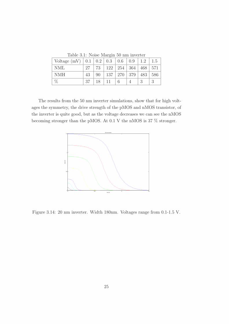
Table 3.1: Noise Margin 50 nm inverterVoltage (mV) 0.1 0.2 0.3 0.6 0.9 1.2 1.5
NML 27 73 122 254 364 468 571
NMH 43 90 137 270 379 483 586
% 37 18 11 6 4 3 3
The results from the 50 nm inverter simulations, show that for high volt-
ages the symmetry, the drive strength of the pMOS and nMOS transistor, of
the inverter is quite good, but as the voltage decreases we can see the nMOS
becoming stronger than the pMOS. At 0.1 V the nMOS is 37 % stronger.
0 0.5 1 1.50
0.5
1
1.5
Vin (V)
Vou
t (V
)
20 nm inverter
Figure 3.14: 20 nm inverter. Width 180nm. Voltages range from 0.1-1.5 V.
25

0 0.01 0.02 0.03 0.04 0.05 0.06 0.07 0.08 0.09 0.1−1.5
−1
−0.5
0
Voltage (V)
Gai
n
Gain 20 nm, 0.1 V
Figure 3.15: Gain of 20 nm inverter, 0.1 V.
0 0.02 0.04 0.06 0.08 0.1 0.12 0.14 0.16 0.18 0.2−3
−2.5
−2
−1.5
−1
−0.5
0
Voltage (V)
Gai
n
Gain 20 nm, 0.2 V
Figure 3.16: Gain of 20 nm inverter, 0.2 V.
0 0.05 0.1 0.15 0.2 0.25 0.3−3.5
−3
−2.5
−2
−1.5
−1
−0.5
0
Voltage (V)
Gai
n
Gain 20 nm, 0.3 V
Figure 3.17: Gain of 20 nm inverter, 0.3 V.
26

0 0.1 0.2 0.3 0.4 0.5 0.6−4
−3.5
−3
−2.5
−2
−1.5
−1
−0.5
0
Voltage (V)
Gai
n
Gain 20 nm, 0.6 V
Figure 3.18: Gain of 20 nm inverter, 0.6 V.
0 0.1 0.2 0.3 0.4 0.5 0.6 0.7 0.8 0.9−4
−3.5
−3
−2.5
−2
−1.5
−1
−0.5
0
Voltage (V)
Gai
n
Gain 20 nm, 0.9 V
Figure 3.19: Gain of 20 nm inverter, 0.9 V.
0 0.2 0.4 0.6 0.8 1 1.2−4
−3.5
−3
−2.5
−2
−1.5
−1
−0.5
0
Voltage (V)
Gai
n
Gain 20 nm, 1.2V
Figure 3.20: Gain of 20 nm inverter, 1.2 V.
27

0 0.5 1 1.5−4
−3.5
−3
−2.5
−2
−1.5
−1
−0.5
0
Voltage (V)
Gai
n
Gain 20 nm, 1.5 V
Figure 3.21: Gain of 20 nm inverter, 1.5 V.
0.1 V 0.2 V 0.3 V 0.6 V 0.9 V 1.2 V 1.5 V0
0.1
0.2
0.3
0.4
0.5
0.6
0.7
Voltages (V)
Noi
se M
argi
n (V
)
Noise Margin 20nm Inverter
Figure 3.22: Noise Margin 20 nm inverter.
0.1 V 0.2 V 0.3 V 0.6 V 0.9 V 1.2 V 1.5 V−60
−40
−20
0
20
40
60
80
100
Voltages (V)
%
Figure 3.23: Noise Margin 20 nm inverter. Difference.
28
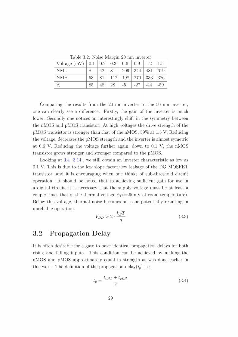
Table 3.2: Noise Margin 20 nm inverterVoltage (mV) 0.1 0.2 0.3 0.6 0.9 1.2 1.5
NML 8 42 81 209 344 481 619
NMH 53 81 112 198 270 333 386
% 85 48 28 -5 -27 -44 -59
Comparing the results from the 20 nm inverter to the 50 nm inverter,
one can clearly see a difference. Firstly, the gain of the inverter is much
lower. Secondly one notices an interestingly shift in the symmetry between
the nMOS and pMOS transistor. At high voltages the drive strength of the
pMOS transistor is stronger than that of the nMOS, 59% at 1.5 V. Reducing
the voltage, decreases the pMOS strength and the inverter is almost symetric
at 0.6 V. Reducing the voltage further again, down to 0.1 V, the nMOS
transistor grows stronger and stronger compared to the pMOS.
Looking at 3.4 3.14 , we still obtain an inverter characteristic as low as
0.1 V. This is due to the low slope factor/low leakage of the DG MOSFET
transistor, and it is encouraging when one thinks of sub-threshold circuit
operation. It should be noted that to achieving sufficient gain for use in
a digital circuit, it is necessary that the supply voltage must be at least a
couple times that of the thermal voltage φT (=25 mV at room temperature).
Below this voltage, thermal noise becomes an issue potentially resulting in
unreliable operation.
VDD > 2 ·
kBT
q(3.3)
3.2 Propagation Delay
It is often desirable for a gate to have identical propagation delays for both
rising and falling inputs. This condition can be achieved by making the
nMOS and pMOS approximately equal in strength as was done earlier in
this work. The definition of the propagation delay(tp) is :
tp =tpHL + tpLH
2(3.4)
29

Figure 3.24: Finding the propagation delay.
Simulations were done on both 50 nm inverters and 20 nm inverters with
voltage 0.6 V and 0.4 V on the 50 nm, 0.6 V and 0.3 V on the 20 nm, and with
different nMOS and pMos widths. The inverter under test was connected to
an identical inverter at the output.
Figure 3.25: Example of measuring the delay. Taken from the 20 nm simu-
lation
30

Width (nm) nMOS, 120 60 pMOS, 120
tpHL(10−12s) 0.99 1.14 1.54
tpLH(10−12s) 2.04 1.76 1.58
tp(10−12s) 1.52 1.45 1.56
Table 3.3: Delay 50 nm inverter, 0.6 V
Width (nm) nMOS, 120 60 pMOS, 120
tpHL(10−12s) 3.16 3.57 4.31
tpLH(10−12s) 8.32 6.36 5.36
tp(10−12s) 5.74 4.965 4.835
Table 3.4: Delay 50 nm inverter, 0.4 V
Width (nm) nMOS, 120 60 pMOS, 180
tpHL(10−12s) 0.40 0.01 0.50
tpLH(10−12s) 1.01 0.73 0.30
tp(10−12s) 0.71 0.37 0.65
Table 3.5: Delay 20 nm inverter, 0.6 V
Width (nm) nMOS, 120 60 pMOS, 180
tpHL(10−12s) 0.34 0.1 0.63
tpLH(10−12s) 2.29 1.92 1.43
tp(10−12s) 1.315 1.01 1.03
Table 3.6: Delay 20 nm inverter, 0.3 V
31

Figure 3.26: Delay for the 20 nm inverter. nMOS width 120 nm vs. 60 nm
pMOS and nMOS.
The results show that we get almost identical propagation delays for both
rising and falling inputs when we use the pMOS widths which we found gave
the best symmetry in the voltage scaling simulations in the previous section.
That said, symmetrical propagation delays does not necessarily mean the
shortest overall delay, as we can see on the results. Looking at det table 3.6
one can see that for the 20 nm inverter, the design with a nMOS width of 120
nm has a longer tpHL than the design where both nMOS and pMOS has the
same width. This would contradict what we earlier have stated, that having
a stronger nMOS would make the tpHL shorter. But looking more closely
at the simulation results 3.26 we see that the design with the larger nMOS
actually has a shorter tpHL. It is clear here that the simulations should have
been run with an input pulse with a faster rise and fall time, so that the
results would be more correct.
32

Chapter 4
Static Random Access
Memory(SRAM)
As the process technology continues to scale, the stability of embedded Static
Random Access Memories (SRAMs) is a growing concern in the design and
test community. Maintaining an acceptable Static Noise Margin (SNM) in
embedded SRAMs while scaling the minimum feature sizes and supply volt-
ages of the Systems-on-a-Chip (SoC) becomes increasingly challenging. Mod-
ern semiconductor technologies push the physical limits of scaling which re-
sults in device patterning challenges and non-uniformity of channel doping.
As a result, precise control of the process parameters becomes exceedingly
difficult and the increased process variations are translated into a wider dis-
tribution of transistor and circuit characteristics. Large SRAM arrays that
are widely used as cache memory in microprocessors and application-specific
integrated circuits can occupy a significant portion of the die area. In an
attempt to optimize the performance/cost ratio of such chips, designers are
faced with a dilemma. Large arrays of fast SRAM help to boost the sys-
tem performance. However, the area impact of incorporating large SRAM
arrays into a chip directly translates into a higher chip cost. Balancing these
requirements is driving the effort to minimize the footprint of SRAM cells.
As a result, millions of minimum-size SRAM cells are tightly packed making
SRAM arrays the densest circuitry on a chip. Such areas on the chip can
be especially susceptible and sensitive to manufacturing defects and process
33

variations. International Technology Roadmap for Semiconductors (ITRS)
[16] [17] predicted
greater parametric yield loss with respect to noise margins
for high density circuits such as SRAM arrays, which are projected to occupy
more than 90% of the SoC area in the next 10 years.
4.1 Random Access Memory(RAM) Cells
The memory array is at the center of the RAM design. Examples of DRAM
and SRAM memory cells are shown in figure 1.2 and 6 Transistor SRAM..
The traditional DRAM memory cell is made up of a pass transistor and a
storage capacitor. Since real capacitors leak charge, the information even-
tually fades unless the capacitor charge is refreshed periodically. Because of
this refresh requirement, it is a dynamic memory as opposed to SRAM. The
CMOS SRAM memory cell is a cross-coupled connection of inverters. The
cross-coupled inverters form a positive feedback circuit, forcing the outputs
in opposite directions. Unlike DRAM, it does not need to be periodically
refreshed, as SRAM uses bistable latching circuitry to store each bit. SRAM
is still volatile in the conventional sense that data is eventually lost when the
memory is not powered.
4.2 SRAM cell design
Cell size minimization is one of the most important design objectives. A
smaller cell allows the number of bits per unit area to be increased and thus,
decreases cost per bit. Reduced cell area can indirectly improve the speed
and power consumption due to the reduction of the associated cell capac-
itances. Smaller cells result in a smaller array area and hence smaller bit
line and word line capacitances, which in turn helps to improve the access
speed performance. Reducing the transistor dimensions is the most effective
means to achieve a smaller cell area. However, the transistor dimensions
cannot be reduced indefinitely without compromising the other parameters.
For instance, smaller transistors can compromise the cell stability. Often,
34

performance and stability objectives restrict arbitrary reduction in cell tran-
sistor sizes. Similarly, cell area can be traded off for special features such as
an improved radiation hardening or multi-port cell access.
Historically, the 4T-polysilicon resistor load cells which are remnants of
the pre-CMOS technologies, where the most used SRAM cell. The main
advantage of static 4T cells with polysilicon resistor load (PRL) was the
approximately 30% smaller area as compared to six-transistor(6T) CMOS
SRAM cells. Due to the higher electron mobility, all transistors in a PRL
cell were normally NMOS. The load resistors served to compensate for the
off-state leakage of the pull-down devices. As the technology scaled into sub-
micron regime (beyond 0.8 µm technology generation), the scalability of a
PRL SRAM cell became an issue. The polysilicon resistor in the PRL cell
could not be scaled as aggressively as the cell’s transistors. Moreover, the ex-
tra technological steps of forming high-resistivity polysilicon are not a part of
the standard CMOS logic technological process. Now the mainstream SRAM
is the 6T SRAM cell. Even though 7T and 8T cell topologies allow for better
cell stability due to their read-disturb-free operation, their implementation
result in a reported 13% and 30% area increase and are therefor not that
common. But as process technologies continue to scale down they may be
more seen in the future.
The 6T CMOS SRAM cell is shown in 4.1. Similarly to one of the im-
plementations of an SR latch, it consists of six transistors. Four transistors
(M1-M4) comprise cross-coupled CMOS inverters and two NMOS transistors
M5 and M6 provide read and write access to the cell. Upon the activation
of the word line, the pass gate transistors connect the two internal nodes of
the cell to the true (BL) and the complementary (BLB) bit lines.
4.3 SRAM operation
Standby
If the word line is not asserted, the access transistors M5 and M6 disconnect
the cell from the bit lines. The two cross coupled inverters formed by M1 Ű
M4 will continue to reinforce each other as long as they are connected to the
35

Figure 4.1: 6 Transistor SRAM.
supply.
Reading
Figure 4.2: Read operation.
Ahead of initiating a read operation, the bit lines are precharged to VDD.
36

The read operation is initiated by enabling the word line (WL) and con-
necting the precharged bit lines, BL and BLB, to the internal nodes of the
cell. Upon read access shown in 4.2, the bit line voltage VBL remains at
the precharge level. The complementary bit line voltage VBLB is discharged
through transistors M1 and M5 connected in series. Transistors M1 and M5
form a voltage divider whose output is now no longer at zero volt and is con-
nected to the input of inverter M2 and M4 4.1. Sizing of M1 and M5 should
ensure that inverter M2 and M4 does not switch causing a destructive read.
In other words, 0+∆V should be less than the switching threshold of inverter
M2 and M4 plus a safety margin or Noise Margin.
Writing
Figure 4.3: Write operation.
The write operation starts with one of the bit lines, BL in 4.3, driven from
precharged value (VDD) to the ground potential by a write driver through
transistor M6. If transistors M4 and M6 are properly sized, then the cell is
flipped and its data is effectively overwritten. The SRAM cell writability is
defined as write margin. Write margin is defined as the minimum voltage
required to flip the state of an SRAM cell. The write margin value and vari-
ation is a function of the cell design, SRAM array size and process variation.
37

4.4 SRAM simulations
To test the SRAM cell performance and stability, a number of simulations
have been done. These simulations have been done on a 50 nm and 20 nm
DG MOSFET transistor setup with varying pMOS gate widths. Vdd was 0.6
V and 0.3 V.
4.4.1 Hold Margin (Retention noise margin)
Retention noise margin (RNM) or hold margin, is the cell static noise margin
(SNM) in the standby mode. In this mode, the bit cell holds data and must
maintain the stable state reinforced by the cross coupled inverters. 6-T cells
present good retention as long as the supply voltage is high enough (data
retention voltage, DRV). In standby mode, the PMOS load transistor (PL)
must be strong enough to compensate for the sub-threshold and gate leakage
currents of all the NMOS transistors connected to the storage node V1 4.1.
Hold stability is commonly quantified by the cell static noise margin (SNM)
in standby mode. The SNM of an SRAM cell represents the minimum DC-
voltage disturbance necessary to upset the cell state, and can be quantified by
the length of the side of the maximum square that can fit inside the butterfly
curves formed by the cross-coupled inverters 4.4.
Figure 4.4: SNM is the length of the sides of the maximum square.
38

0 0.1 0.2 0.3 0.4 0.5 0.60
0.1
0.2
0.3
0.4
0.5
V1 (V)
V2 (V
)
Figure 4.5: Static Noise Margin for a 50 nm SRAM W = 60 nm, 0.6 V.
0 0.1 0.2 0.3 0.4 0.5 0.60
0.1
0.2
0.3
0.4
0.5
V1 (V)
V2 (V
)
Figure 4.6: Static Noise Margin for a 50 nm SRAM W = 120 nm, 0.6 V.
39

0 0.05 0.1 0.15 0.2 0.25 0.30
0.05
0.1
0.15
0.2
0.25
V1 (V)
V2 (V
)
Figure 4.7: Static Noise Margin for a 50 nm SRAM W = 60 nm, 0.3 V.
0 0.05 0.1 0.15 0.2 0.25 0.30
0.05
0.1
0.15
0.2
0.25
V1 (V)
V2
(V)
Figure 4.8: Static Noise Margin for a 50 nm SRAM W = 120 nm, 0.3 V.
0 0.1 0.2 0.3 0.4 0.5 0.60
0.1
0.2
0.3
0.4
0.5
0.6
V1(1)
V2
(V)
Figure 4.9: Static Noise Margin for a 20 nm SRAM W = 60 nm, 0.6 V.
40

0 0.1 0.2 0.3 0.4 0.5 0.60
0.1
0.2
0.3
0.4
0.5
V1 (V)
V2
(V)
Figure 4.10: Static Noise Margin for a 20 nm SRAM W = 120 nm, 0.6 V.
0 0.1 0.2 0.3 0.4 0.5 0.60
0.1
0.2
0.3
0.4
0.5
V1 (V)
V2
(V)
Figure 4.11: Static Noise Margin for a 20 nm SRAM W = 180 nm, 0.6 V.
0 0.05 0.1 0.15 0.2 0.25 0.30
0.05
0.1
0.15
0.2
0.25
V1 (V)
V2
(V)
Figure 4.12: Static Noise Margin for a 20 nm SRAM W = 60 nm, 0.3 V.
41

0 0.05 0.1 0.15 0.2 0.25 0.30
0.05
0.1
0.15
0.2
0.25
V1 (V)
V2
(V)
Figure 4.13: Static Noise Margin for a 20 nm SRAM W = 120 nm, 0.3 V.
0 0.05 0.1 0.15 0.2 0.25 0.30
0.05
0.1
0.15
0.2
0.25
V1 (V)
V2
(V)
Figure 4.14: Static Noise Margin for a 20 nm SRAM W = 180 nm, 0.3 V.
42

As we can see from the results, with the supply voltages of 0.6 V and 0.3
V, the SRAM cells manages to hold the data stored in the cell. This is due
to the high gain of the cross-coupled inverters and the pass gates, which was
established in Chapter 3.
4.4.2 Read Margin(RM)
During a read operation, V1 rises above 0V, to a voltage determined by
the resistive voltage divider set up by the pass gate transistor (M5) and the
pull-down transistor (M1) between BL and node V1 4.2. The ratio of the
strength ratio between M1 and M5 determines how high V1 will rise. If V1
exceeds the trip point of the inverter formed by M4 and M2, the cell bit will
flip during the read operation, causing a read upset. Read stability can also
be quantified by the cell SNM during a read access. Since M5 operates in
parallel to M3 and keeps M1 from ever reaching 0V, the gain in the inverter
transfer characteristic will decrease, causing a reduction in the separation
between the butterfly curves and thus in SNM. For this reason, the cell is
considered most vulnerable to noise during the read access. The read margin
can be increased by up sizing the pull-down transistor, which results in an
area penalty and/or increasing the gate length of the pass gate transistor,
which increases the WL delay and hurts the write margin as we will later be
established.
0 0.1 0.2 0.3 0.4 0.5 0.60
0.1
0.2
0.3
0.4
0.5
V1 (V)
V2 (V
)
Figure 4.15: Read Noise Margin for a 50 nm SRAM W = 60 nm, 0.6 V.
43

0 0.1 0.2 0.3 0.4 0.5 0.60
0.1
0.2
0.3
0.4
0.5
V1 (V)
V2 (V
)
Figure 4.16: Read Noise Margin for a 50 nm SRAM W = 120 nm, 0.6 V.
0 0.05 0.1 0.15 0.2 0.25 0.30
0.05
0.1
0.15
0.2
0.25
V1 (V)
V2 (V
)
Figure 4.17: Read Noise Margin for a 50 nm SRAM W = 60 nm, 0.3 V.
44

0 0.05 0.1 0.15 0.2 0.25 0.30
0.05
0.1
0.15
0.2
0.25
V1 (V)
V2
(V)
Figure 4.18: Read Noise Margin for a 50 nm SRAM W = 120 nm, 0.3 V.
0 0.1 0.2 0.3 0.4 0.5 0.60
0.1
0.2
0.3
0.4
0.5
V1 (V)
V2
(V)
Figure 4.19: Read Noise Margin for a 20 nm SRAM W = 60 nm, 0.6 V.
0 0.1 0.2 0.3 0.4 0.5 0.60
0.1
0.2
0.3
0.4
0.5
V1 (V)
V2
(V)
Figure 4.20: Read Noise Margin for a 20 nm SRAM W = 120 nm, 0.6 V.
45

0 0.05 0.1 0.15 0.2 0.25 0.30
0.05
0.1
0.15
0.2
0.25
V1 (V)
V2
(V)
Figure 4.21: Read Noise Margin for a 20 nm SRAM W = 60 nm, 0.3 V.
0 0.05 0.1 0.15 0.2 0.25 0.30
0.05
0.1
0.15
0.2
0.25
V1 (V)
V2
(V)
Figure 4.22: Read Noise Margin for a 20 nm SRAM W = 120 nm, 0.3 V.
46

The results of the simulations shows that the NM is quite small for the 20
nm SRAM cell and not much additional voltage is required to make the cell
become unstable. Increasing the pMOS width improves NM as is expected.
4.4.3 Write Margin(WM)
During a write operation, M5 and M3 form a resistive voltage divider between
the low-going BLB and node V1 4.3. If the voltage divider pulls VL below the
trip point of the inverter formed by M4 and M2, a successful write operation
occurs. The write margin can be measured as the maximum BLB voltage
that is able to flip the cell state while BL is kept high. The write margin can
be improved by keeping the pull-up device minimum sized and up sizing the
pass gate transistor W/L at the cost of cell area and the cell read margin.
0 0.1 0.2 0.3 0.4 0.5 0.60
0.1
0.2
0.3
0.4
0.5
V1 (V)
V2 (V
)
Figure 4.23: Write Noise Margin for a 50 nm SRAM W = 60 nm, 0.6 V.
0 0.1 0.2 0.3 0.4 0.5 0.60
0.1
0.2
0.3
0.4
0.5
V1 (V)
V2 (V
)
Figure 4.24: Write Noise Margin for a 50 nm SRAM W = 120 nm, 0.6 V.
47

0 0.05 0.1 0.15 0.2 0.25 0.30
0.05
0.1
0.15
0.2
0.25
V1 (V)
V2 (V
)
Figure 4.25: Write Noise Margin for a 50 nm SRAM W = 60 nm, 0.3 V.
0 0.05 0.1 0.15 0.2 0.25 0.30
0.05
0.1
0.15
0.2
0.25
V1 (V)
V2
(V)
Figure 4.26: Write Noise Margin for a 50 nm SRAM W = 120 nm, 0.3 V.
0 0.1 0.2 0.3 0.4 0.5 0.60
0.1
0.2
0.3
0.4
0.5
V1 (V)
V2
(V)
Figure 4.27: Write Noise Margin for a 20 nm SRAM W = 60 nm, 0.6 V.
48

0 0.1 0.2 0.3 0.4 0.5 0.60
0.1
0.2
0.3
0.4
0.5
V1 (V)
V2
(V)
Figure 4.28: Write Noise Margin for a 20 nm SRAM W = 120 nm, 0.6 V.
0 0.1 0.2 0.3 0.4 0.5 0.60
0.1
0.2
0.3
0.4
0.5
V1 (V)
V2
(V)
Figure 4.29: Write Noise Margin for a 20 nm SRAM W = 180 nm, 0.6 V.
0 0.05 0.1 0.15 0.2 0.25 0.30
0.05
0.1
0.15
0.2
0.25
V1 (V)
V2
(V)
Figure 4.30: Write Noise Margin for a 20 nm SRAM W = 60 nm, 0.3 V.
49

0 0.05 0.1 0.15 0.2 0.25 0.30
0.05
0.1
0.15
0.2
0.25
V1 (V)
V2
(V)
Figure 4.31: Write Noise Margin for a 20 nm SRAM W = 120 nm, 0.3 V.
0 0.05 0.1 0.15 0.2 0.25 0.30
0.05
0.1
0.15
0.2
0.25
V1 (V)
V2
(V)
Figure 4.32: Write Noise Margin for a 20 nm SRAM W = 180 nm, 0.3 V.
50

DGSG
5.8 6 6.2 6.4 6.6 6.8
x 10−11
0
0.1
0.2
0.3
0.4
0.5
0.6
Time (s)
Vo
lta
ge
(V
)
Write Operation
50 nm20 nm20 nm50 nm
Figure 4.33: Switching delay during write.
Looking at the NM of the write operation, one can see that with this
kind of transistor sizing the NM is quite good and that increasing the width
of the pMOS transistors at best only keeps the NM at the same level but
also reduces the NM during write. The earlier assumptions that a high NM
during write means a lower NM during read, is confirmed in these simulations.
Looking at the write delay, one can also see that what we learned in chapter
3 is correct. Reducing the VDD also increases the delay and the 20 nm
DG MOSFET SRAM circuit has a faster switching time then the 50 nm
counterpart. Next pages show a comparison of the NMs 4.34 4.35 4.36 4.37.
51

R S W0
50
100
150
200
250
300Noise Margin 50 nm 0.6 V
Noi
se M
argi
n (m
V)
60 nm120 nm
Figure 4.34: Noise Margin for a 50 nm SRAM. Comparing W = 60 nm and
W = 120 nm, 0.6 V.
R S W0
20
40
60
80
100
120
140Nosise Margin 50 nm 0.3 V
Noi
se M
argi
n (m
V)
60 nm120 nm
Figure 4.35: Noise Margin for a 50 nm SRAM. Comparing W = 60 nm and
W = 120 nm, 0.3 V.
52

R S W0
50
100
150
200
250Noise Margin 20 nm 0.6 V
Noi
se M
argi
n (m
V)
60 nm120 nm180 nm
Figure 4.36: Noise Margin for a 20 nm SRAM. Comparing W = 60 nm, W
= 120 nm and 180 nm, 0.6 V.
R S W0
20
40
60
80
100
120
140Noise Margin 20 nm 0.3 V
Noi
se M
argi
n (m
V)
60 nm120 nm180 nm
Figure 4.37: Noise Margin for a 20 nm SRAM. Comparing W = 60 nm, W
= 120 nm and 180 nm, 0.3 V.
53

4.5 DG MOSFET as a Four Terminal Device
During the read operation, in general, a large current drivability ratio of
the driver to the pass gate M1/M3 and M2/M4 is preferred to reduce read
disturbance and enhance the read margin. On the other hand, during the
write operation, strong pass gates are desired to easily flip the potential at
the memory node and to enhance the WM. These requirements for larger
RM and WM contradict each other in conventional use of a MOSFET/DG
MOSEFET transistor. But due to the specific design of the DG MOSFET,
one has the possibility to use the gates independently to tune the Vth and
drivability of the pass gate 4.38. By keeping the bottom gate of the DG
MOSFET at gnd during the read operation, the drivability of the pass gate
is reduced and hence, the RM is enhanced.
0 0.2 0.4 0.6 0.8 1 1.2
−10−3
−10−4
−10−5
−10−6
−10−7
−10−8
−10−9
−10−10
Voltage (V)
Dra
in V
urra
nt (
A)
Drain current 50nm
Figure 4.38: Drain current for the 50 nm DG nMOS transistor. The lowest
curve is the transistor working as four terminal device where one gate is
contacted to gnd.
54

0 0.1 0.2 0.3 0.4 0.5 0.60
0.1
0.2
0.3
0.4
0.5
V1(1)
V2
(V)
Read Noise Margin 50nm 0.6 V
60 nm sg60 nm
Figure 4.39: Read Noise Margin for a 50 nm SRAM. Comparing dg and sg
configuration. W = 60 nm, 0.6 V.
0 0.1 0.2 0.3 0.4 0.5 0.60
0.1
0.2
0.3
0.4
0.5
V1(1)
V2
(V)
Read Noise Margin 50nm 0.6 V
120 nm120 nm sg
Figure 4.40: Read Noise Margin for a 50 nm SRAM. Comparing dg and sg
configuration. W = 120 nm, 0.6 V.
0 0.05 0.1 0.15 0.2 0.25 0.30
0.05
0.1
0.15
0.2
0.25
V1(1)
V2
(V)
60 nm60 nm sg
Figure 4.41: Read Noise Margin for a 50 nm SRAM. Comparing dg and sg
configuration. W = 60 nm, 0.3 V.
55

0 0.05 0.1 0.15 0.2 0.25 0.30
0.05
0.1
0.15
0.2
0.25
V1(1)
V2
(V)
120 nm120 nm sg
Figure 4.42: Read Noise Margin for a 50 nm SRAM. Comparing dg and sg
configuration. W = 120 nm, 0.3 V.
0 0.1 0.2 0.3 0.4 0.5 0.60
0.1
0.2
0.3
0.4
0.5
V1(1)
V2
(V)
60 nm60 nm sg
Figure 4.43: Read Noise Margin for a 20 nm SRAM. Comparing dg and sg
configuration. W = 60 nm, 0.6 V.
0 0.1 0.2 0.3 0.4 0.5 0.60
0.1
0.2
0.3
0.4
0.5
V1(1)
V2
(V)
Read Noise Margin 20nm 0.6 V
120 nm120 nm sg
Figure 4.44: Read Noise Margin for a 20 nm SRAM. Comparing dg and sg
configuration. W = 120 nm, 0.6 V.
56

0 0.1 0.2 0.3 0.4 0.5 0.60
0.1
0.2
0.3
0.4
0.5
V1(1)
V2
(V)
Read Noise Margin 20nm 0.6 V
180 nm180 nm sg
Figure 4.45: Read Noise Margin for a 20 nm SRAM. Comparing dg and sg
configuration. W = 180 nm, 0.6 V.
0 0.05 0.1 0.15 0.2 0.25 0.30
0.05
0.1
0.15
0.2
0.25
V1(1)
V2
(V)
60 nm sg60 nm
Figure 4.46: Read Noise Margin for a 20 nm SRAM. Comparing dg and sg
configuration. W = 60 nm, 0.3 V.
0 0.05 0.1 0.15 0.2 0.25 0.30
0.05
0.1
0.15
0.2
0.25
V1(1)
V2
(V)
120 nm120 nm sg
Figure 4.47: Read Noise Margin for a 20 nm SRAM. Comparing dg and sg
configuration. W = 120 nm, 0.3 V.
57

0 0.05 0.1 0.15 0.2 0.25 0.30
0.05
0.1
0.15
0.2
0.25
V1(1)
V2
(V)
180 nm sg180 nm
Figure 4.48: Read Noise Margin for a 20 nm SRAM. Comparing dg and sg
configuration. W = 180 nm, 0.3 V.
DGSG
0 0.5 1 1.5 2 2.5 3
x 10−10
−0.1
0
0.1
0.2
0.3
0.4
0.5
0.6
0.7
Time (s)
Vol
tage
(V
)
Read Operation, 50nm , 0.6V
DGSG
Figure 4.49: Read Cycle for a 50 nm SRAM. Comparing dg and sg configu-
ration. W = 60 nm, 0.6 V.
DGSG
0 0.5 1 1.5 2 2.5 3
x 10−10
−0.1
0
0.1
0.2
0.3
0.4
0.5
0.6
0.7
Time (s)
Vol
tage
(V
)
Read Operation, 20nm , 0.6V
DGSG
Figure 4.50: Read Cycle for a 20 nm SRAM. Comparing dg and sg configu-
ration. W = 60 nm, 0.6 V.
58

0 0.5 1 1.5 2 2.5 3
x 10−10
−0.05
0
0.05
0.1
0.15
0.2
0.25
0.3
0.35
Time (s)V
olta
ge (
V)
Read Operation, 50nm , 0.3 V
DGSG
Figure 4.51: Read Cycle for a 50 nm SRAM. Comparing dg and sg configu-
ration. W = 60 nm, 0.3 V.
0 0.5 1 1.5 2 2.5 3
x 10−10
−0.05
0
0.05
0.1
0.15
0.2
0.25
0.3
0.35
Time (s)
Vol
tage
(V
)
Read Operation, 20nm , 0.3 V
SGDG
Figure 4.52: Read Cycle for a 20 nm SRAM. Comparing dg and sg configu-
ration. W = 60 nm, 0.3 V.
0.3 V, W = 60 nm 0.3 V, W = 120 nm 0.6 V, W = 60 nm 0.6 V, W = 120 nm0
0.02
0.04
0.06
0.08
0.1
0.12
0.14
0.16
0.18
0.2Noise Margin, Read, 50 nm
Vol
tage
(V
)
SGDG
Figure 4.53: Read Noise Margin for a 50 nm SRAM. Comparing dg and sg
configuration. W = 60 nm
59

0.3 V, W = 60nm 0.3 V, W = 120nm 0.3 V, W = 180nm 0.6 V, W = 60nm 0.6 V, W = 120nm 0.6 V, W = 180nm0
0.02
0.04
0.06
0.08
0.1
0.12
Vol
tage
(V
)
NM, Read Operation, 20 nm
SGDG
Figure 4.54: Read Noise Margin for a 20 nm SRAM. Comparing dg and sg
configuration. W = 60 nm
After this modification, NM during read operation increases, which is
very good results. Keeping in mind that the write NM and static NM are
unchanged, this is a very encouraging result, indeed.
60

Chapter 5
Conclusion
In this thesis the DG MOSFET has undergone a large number of simulations
using Silvaco ATLAS and MixedMode software. We have determined the
combination of gate work functions which gives the most desirable point of
operation. It has also been shown that in order to get the required voltage
transfer characteristic of the DG MOSFET CMOS inverter, one has to take
into account the operation voltage in the design and the process pitch size,
because the transistors driving strengths ratio changes when these variables
change. We have shown that DG MOSFET transistor can be used in a 6-T
SRAM design and that it will function correctly at a gate length of 20 nm.
Changing the ratio between nMOS and pMOS transistors can be beneficial
to during some part of the SRAM operation (read operation) but has adverse
effect on other operations. The 20 nm SRAM cell is faster than the 50 nm cell,
but has a smaller NM and is therefor more sensible to external noise, thermal
noise and process variation. Using the DG MOSFET as a four terminal device
during read operations show a significant performance increase which is not
possible with planar MOSFETs and this ability should be one that will make
the DG MOSFET a very god candidate to replace the bulk CMOS transistor
as the leading transistor design in SRAM cells. It should also be noted that
variability studies on Multigate Field Effect Transistor (MUGFET) SRAM
cells have shown much lower statistical variation than planar bulk MOS-based
SRAM cells[18][19][20][21], which is important as the NM also decreases when
the operating voltage decreases.
61

62
Chapter 6
Future Work
The results of the simulations in this work have not taken into account neither
temperature variations or processing variations. This thesis has also not
looked at leakage currents or power consumption, but MUGFET devices
considerably reduce the leakage currents as compared to the planar bulk
devices[22]. To fully test the DG MOSFET in SRAM design, one should
take these points into consideration.
6.1 Development of SPICE-type models
The simulations done in this thesis are all MixedMode simulation. Though
they can be very accurate and detailed, they are very time consuming to carry
out, and the hardware requirements for running simulations of larger circuits
are high. This calls for the development of SPICE-type models which can
be used for circuit development and testing. As we all know, time is money,
and this is especially true in the field of electronics where the developments
goes on in an extreme speed. Reducing the development cost in this business
is just as important as in others.
63

6.2 MUGFET Z-RAM
One of the candidates for the next generation of memory architecture is the
Z-RAM1. Z-RAM is a form of DRAM device which, as the name implies,
does not use a capacitor to store the charge, but instead uses the floating
body as its own storage cell. This, of course, reduces the size of the memory
cell and it is reported to have longer retention time[23]. It would be very
interesting to use simulation tools like ATLAS to test different configurations
of MUGFET design for use in this type of memory.
1Z-RAM or Zero capacitor RAM
64

Appendix A
SINANO template
The European union research project Silicon Nano-devices (SINANO) has
defined a template for a double-gate device.
A.1 Template description
The device is based on a symmetrical doping profile for both source and drain
with the same Gaussian characteristic. Doping of the bulk case is a mirroring
of the top process.
P-type uniform substrate doping:Body acceptor concentration: NS = 1·1015cm−3
N(x, y) = G(y) · L(x) (A.1)
All injections have a Gaussian profile with an implant of NPEAK = 1·1020cm−3
N-type source extension profile:Standard deviation: σy = 5.64·10−3µm
G(y) = NPEAKe−
1
2[ y
σy]2; y > 0 (A.2)
L(x) = 1; x < x0 (A.3)
L(x) = NPEAKe−
1
2[
x−x0
0.28σy]2; x > x0 (A.4)
65

N-type source contact profile:Standard deviation: σy = 1.12·10−2µm
G(y) = NPEAKe−
1
2[ y
σy]2; y > 0 (A.5)
L(x) = 1; x < x0 (A.6)
L(x) = NPEAKe−
1
2[
x−x0
0.35σy]2; x > x0 (A.7)
Figure A.1: Source to drain cuts of doping profile at the silicon/oxide bound-
ary(blue) and at the center symmetry line.
As can be seen in the doping profile in figure A.1, the lateral profile drops
very fast towards the center. While the target profile for the 65nm node
is 2.8nm/decade according to the ITRS roadmap, the source extension first
drop close to this target, but it approaches 0.7nm/decade into the body.
Compact modeling of physical mechanisms in doping profiles is difficult. To
simplify, a piecewise equipotential boundary around the device is desirable.
An ideal device has been created, based on the template device. The dop-
ing profiles at the contacts of the template device is replaced with ideal n+
66
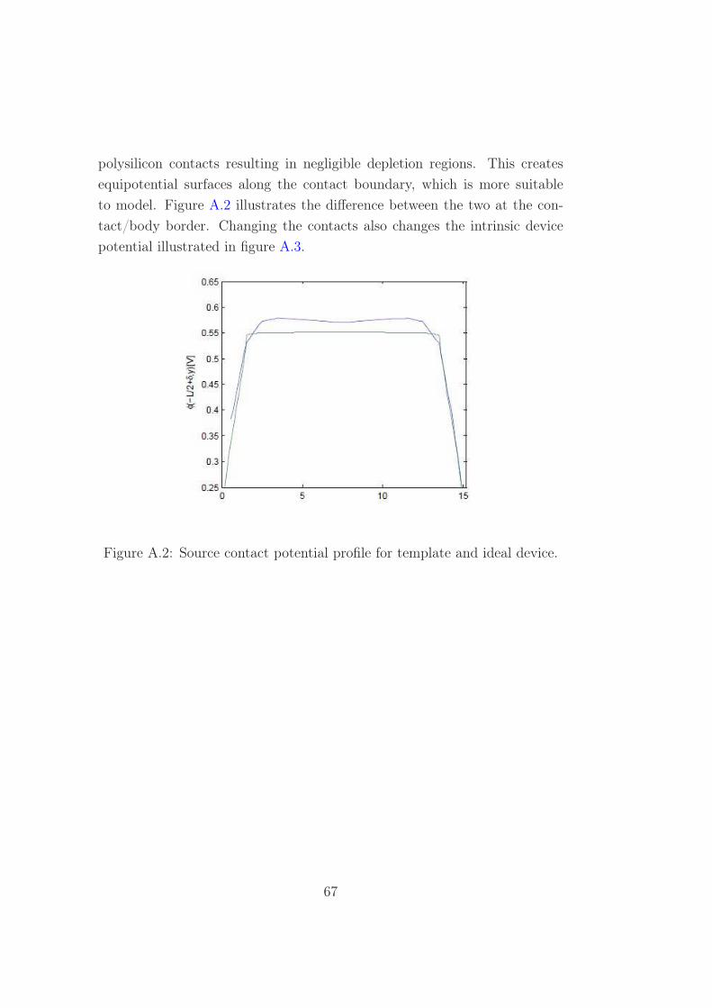
polysilicon contacts resulting in negligible depletion regions. This creates
equipotential surfaces along the contact boundary, which is more suitable
to model. Figure A.2 illustrates the difference between the two at the con-
tact/body border. Changing the contacts also changes the intrinsic device
potential illustrated in figure A.3.
Figure A.2: Source contact potential profile for template and ideal device.
67

Figure A.3: Source to drain potential profile at the center symmetry line for
template and ideal device.
68

Appendix B
Atlas simulation files
B.1 Atlas device model
* Double gate Mosfet
go atlas
set L=0.050
set H=0.012
set tox = 0.0016
set contactW = 0.001
set sourceStart = $L/2
set sourceEnd = $L/2 + $contactW
set drainStart = -$L/2 - $contactW
set drainEnd = -$L/2
set deviceLenghtMiddle = 0
set deviceHeightEnd = $H + $tox
set deviceHeightMiddle = $H/2
set meshSpacingHD = $L/250
set meshSpacingLD = $L/50
set GGCut0=-5*$L/10
set GGCut1=-4*$L/10
69

set GGCut2=-3*$L/10
set GGCut3=-2*$L/10
set GGCut4=-$L/10
set GGCut5=0
set GGCut6=$L/10
set GGCut7=2*$L/10
set GGCut8=3*$L/10
set GGCut9=4*$L/10
set GGCut10=5*$L/10
mesh space.mult=2
x.mesh l=$drainStart s=$meshSpacingHD
x.mesh l=$drainEnd s=$meshSpacingHD
x.mesh l=$deviceLenghtMiddle s=$meshSpacingLD
x.mesh l=$L/2 s=$meshSpacingHD
x.mesh l=$sourceEnd s=$meshSpacingHD
y.mesh l=-$tox s=$meshSpacingHD
y.mesh l=0 s=$meshSpacingHD
y.mesh l=$deviceHeightMiddle s=$meshSpacingLD
y.mesh l=$H s=$meshSpacingHD
y.mesh l=$deviceHeightEnd s=$meshSpacingHD
region num=1 x.min=$drainEnd x.max=$sourceStart y.min=0 y.max=$H
silicon
region num=2 x.min=$drainStart x.max=$sourceEnd y.min=-$tox y.max=0
sio2
region num=3 x.min=$drainStart x.max=$sourceEnd y.min=$H y.max=$deviceHeightEnd
sio2
region num=4 x.min=$drainStart x.max=$drainEnd y.min=0 y.max=$H sil-
icon
region num=5 x.min=$sourceStart x.max=$sourceEnd y.min=0 y.max=$H
silicon
elec name=gatetop x.min=$drainEnd x.max=$sourceStart y.min=$deviceHeightEnd
70

y.max=$deviceHeightEnd+0.01
elec name=gatebottom x.min=$drainEnd x.max=$sourceStart y.min=-0.01-
$tox y.max=-$tox
elec name=drain x.min=$drainStart-0.001 x.max=$drainStart y.min=0 y.max=$H
elec name=source x.min=$sourceEnd x.max=$sourceEnd+0.001 y.min=0 y.max=$H
material region=2 permittivity=7
material region=3 permittivity=7
contact name=gatetop workfun=4.53
contact name=gatebottom workfun=4.53 common=gatetop
doping uniform conc=1.0E15 p.type region=1
doping uniform conc=1.0E20 n.type region=4
doping uniform conc=1.0E20 n.type region=5
structure outfile=dgnmos50nm.str
plot the structure
models boltz
method newton
solve init
solve vdrain=0.1
save outf=dgnmos50nm2.str
tonyplot dgnmos50nm2.str
* Bias the drain
solve vdrain=0.1
* Ramp the gate
log outf=dgnmos50nm1.log master
solve vgatetop=0 vstep=-0.05 vfinal=-0.5 name=gatetop
save outf=dgnmos50nm1.str
log outf=dg2nmos50nm1.log master
71

solve vgatetop=0 vstep=0.05 vfinal=1.5 name=gatetop
save outf=dg2nmos50nm1.str
tonyplot dg2nmos50nm1.log -set dg2nmos50nm1log.set
* extract device parameters
extract name=nvtn (xintercept(maxslope(curve(abs(v.gatetop),abs(i.drain))))
- abs(ave(v.drain))/2.0)
quit
B.2 MixedMode circuit file
go atlas
.begin
*
* SRAM CIRCUIT simulation
*
*
* Circuit description
*
ap1 V1=drain V2=gatetop V2=gatebottom Vdd=source infile=dgpmos50.str
width=0.06
an1 V1=drain V2=gatetop V2=gatebottom gnd=source infile=dgnmos50.str
width=0.06
ap2 V2=drain V1=gatetop V1=gatebottom Vdd=source infile=dgpmos50.str
width=0.06
an2 V2=drain V1=gatetop V1=gatebottom gnd=source infile=dgnmos50.str
width=0.06
an3 bl=drain WL=gatetop WL=gatebottom V1=source infile=dgnmos50.str
width=0.06
72

an4 blb=drain WL=gatetop WL=gatebottom V2=source infile=dgnmos50.str
width=0.06
c1 bl gnd 0.5ff
c2 blb gnd 0.5ff
vVdd Vdd gnd DC 0.6
vWL WL gnd PULSE(0 0.6 19ps 1ps 1ps 18ps 40ps)
vbl bl gnd Pulse(0 0.6 20ps 1ps 1ps 40ps 80ps)
vblb blb gnd Pulse(0.6 0 20ps 1ps 1ps 40ps 80ps)
*
* End of circuit description
*
.nodeset v(V1)=0.6 v(V2)=0
.numeric vchange=0.1 toltr=1e-3 toldc=1e-1 lte=0.15 dtmin=0.5e-13 imaxdc=40
imaxtr=40 VMAX=2 VMIN=-2
.log outfile=write
.ic v(V1)=0.6 v(V2)=0
.tran 0.2ps 150ps uic
.end
*
* ATLAS device models and parameters
*
contact name=gatetop workfun=4.53 device=an1
contact name=gatebottom workfun=4.53 common=gatetop device=an1
contact name=gatetop workfun=4.9 device=ap1
contact name=gatebottom workfun=4.9 common=gatetop device=ap1
contact name=gatetop workfun=4.53 device=an2
contact name=gatebottom workfun=4.53 common=gatetop device=an2
73

contact name=gatetop workfun=4.9 device=ap2
contact name=gatebottom workfun=4.9 common=gatetop device=ap2
contact name=gatetop workfun=4.53 device=an3
contact name=gatebottom workfun=4.53 common=gatetop device=an3
contact name=gatetop workfun=4.53 device=an4
contact name=gatebottom workfun=4.53 common=gatetop device=an4
models boltz print
method newton trap
go atlas
quit
74
Bibliography
[1] G.E. Moore. Cramming more components onto integrated circuits. Elec-
tronics, 38, 1965.
[2] C. Mead B. Hoeneisen. Fundumental limitations in microelectronics-i.
mos technology. Solid-State Electronics, 15:819–829, 1972.
[3] B. Davari. Cmos technology: present and future. Symp. VLSI Circuits
Digest Tech. Papers, pages 5–10, 1999.
[4] S. Thompson, P. Packan, and M. Bohr. Mos scaling: Transistor chal-
lenges for the 21st century. Intel Technol. J., (Q3):1–19, 1998.
[5] International technology roadmap for semiconductors - 2008 (itrs-2008)
update, 2008. http://www.itrs.net/.
[6] H.-S.P. Wong, D.J. Frank, and P.M. Solomon. Device design consid-
erations for double-gate, ground-plane, and single-gated ultra-thin soi
mosfet’s at the 25 nm channel length generation. In Electron Devices
Meeting, 1998. IEDM ’98 Technical Digest., International, pages 407–
410, 1998.
[7] L. Chang and C. Hu. Mosfet scaling into the 10 nm regime. Proc.
Nanoelectronic Workshop, pages 351–355, 2000.
[8] L. Chang, S. Tang, T. J. King, J. Bokor, and C. Hu. Gate length scaling
and threshold voltage control of double-gate mosfets. IEDM tech. Dig.,
pages 719–722, 2000.
75

[9] A. Klös and A. Kostka. A new analytical method of solving 2d poisson’s
equation in mos devices applied to threshold voltage and subthreshold
modeling. 39(12):1761–1775, December 1996.
[10] J Østhaug, T A Fjeldly, and B Iñiguez. Closed-form 2d modeling of
sub-100nm mosfets in the subthreshold regime. Journal of Telecommu-
nications and Information Technology, 1:70–79, 2004.
[11] S. Kolberg. Modeling of Electrostatics and Drain Current in Nanoscale
Double-Gate MOSFETs. PhD thesis, Norwegian University of Science
and Technology, 2007.
[12] S. Kolberg and T. A. Fjeldly. 2d modeling of nanoscale dg soi mosfets in
and near the subthreshold regime. Journal of Computational Electronics,
5:217–222, 2006.
[13] S. Kolberg and T. A. Fjeldly. 2d modeling of nanoscale double gate
soi mosfets using conformal mapping. Physica Scripta, T125(Topical
issue):1–4, 2006.
[14] S. Kolberg, T. A. Fjeldly, and B. Iniguez. Self-consistent 2d compact
model for nanoscale double gate mosfets. Lecture Notes in Computer
Science, 3994:607 – 614, May 2006.
[15] P. et al Ranade. Molybdenum as a gate electrode for deep sub-micron
cmos technology. Mat. Res. Soc. Symp., 611, 2000.
[16] International technology roadmap for semiconductors - 2003 (itrs-2003),
2003. http://public.itrs.net/.
[17] International technology roadmap for semi-
conductors - 2004 (itrs-2004) update, 2004.
http://www.itrs.net/common/2004update/2004update.htm.
[18] A. Yagishita. Finfet sram process technology for hp32 nm node and
beyond. IEEE Int. Conf. on Integrated Circuit Design and Technology,
page 1Ű4, 2007.
76

[19] Z. Guo, S. Balasubramaniam, R. Zlatanovici, T-J. King, and B. Nikolic.
Finfet based sram design. Int. Symp. on Low Power Electronics and
Design, page 2Ű7, 2005.
[20] S-H. Kim and J. G. Fossum. Design optimization and performance
projections of double-gate finfets with gate-source/drain underlap for
sram applications. IEEE Trans. Electron Devices, 54:1934Ű1942, 2007.
[21] R. et al Tsuchiya. Controllable inverter delay and suppressing vth fluc-
tuation technology in silicon on thin box featuring dual back-gate bias
architecture. IEDM Tech. Dig., page 475Ű478, 2007.
[22] O Thomas, M. Reyboz, and M. Belleville. Sub-1 v, robust and compact
6-t sram cell in double-gate mos technology. IEEE Int. Symp. on Circuits
and Systems, pages 2778–2781, 2007.
[23] T.S Jang, J.S. Kim, S.M Hwang, Y.H. Oh, K.M. Rho, S.J. Chung, S.O.
Chung, and J.G. et al Oh. Highly scalable z-ram with remarkably long
data retention for dram application, 2009.
77