nanomechanical actuation using molecular forces … · nanomechanical actuation using molecular...
TRANSCRIPT

NANOMECHANICAL ACTUATION USING MOLECULAR FORCES
OF AMINO AZO BENZENE DYE
A DISSERTATION
SUBMITTED TO THE DEPARTMENT OF MECHANICAL
ENGINEERING
AND THE COMMITTEE ON GRADUATE STUDIES
OF STANFORD UNIVERSITY
IN PARTIAL FULFILLMENT OF THE REQUIREMENTS
FOR THE DEGREE OF
DOCTOR OF PHILOSOPHY
A. Joseph Rastegar
March 2014

This dissertation is online at: http://purl.stanford.edu/pb694jt6024
© 2014 by Ali Joseph Rastegar. All Rights Reserved.
Re-distributed by Stanford University under license with the author.
ii

I certify that I have read this dissertation and that, in my opinion, it is fully adequatein scope and quality as a dissertation for the degree of Doctor of Philosophy.
Beth Pruitt, Primary Adviser
I certify that I have read this dissertation and that, in my opinion, it is fully adequatein scope and quality as a dissertation for the degree of Doctor of Philosophy.
Nicholas Melosh, Co-Adviser
I certify that I have read this dissertation and that, in my opinion, it is fully adequatein scope and quality as a dissertation for the degree of Doctor of Philosophy.
Roger Howe
Approved for the Stanford University Committee on Graduate Studies.
Patricia J. Gumport, Vice Provost for Graduate Education
This signature page was generated electronically upon submission of this dissertation in electronic format. An original signed hard copy of the signature page is on file inUniversity Archives.
iii

Abstract
The emerging fields of nanomotors and optomechanics are based on the harnessing of
light to generate force. However, our ability to detect the changes in material properties
as a result of these forces (such as small surface stresses) is limited by temperature
drift, environmental noise, and low-frequency flicker electronic noise. To addresses these
limitations, we functionalized microfabricated silicon cantilevers with an azo dye, silane-
based self-assembled monolayer. We developed a fast, one pot, simple, room-temperature
linkage chemistry to connect methyl red (the actuator) to 3-aminopropyltriethoxysilane (a
silicon attachment) to form (E)-2-((4-(dimethylamino)phenyl)diazenyl) -N- (3(triethoxysi-
lyl)propyl)benzamide (MR-APTES). These molecules change their shape when exposed to
light at specific wavelengths, enabling modulation of surface stress by light.
Atomic force microscopy, contact angle analysis, ellipsometry, and X-ray photoelectron
spectroscopy verified successful assembly of molecules on the cantilever. Ultraviolet and
visible spectra demonstrated optical switching of the synthesized molecule in solution.
MR-APTES was then used to form a self assembled monolayer (1 nm thick) on surface
of a silicon cantilever of 500 µm long 100 µm wide and 1 µm thick. The optical-mechanical
actuation of cantilever surface stress was observed by exciting the MR-APTES with a
405 nm laser and optically monitoring tip deflection, allowing us to measure forces of
approximately 0.3 pN per molecule. Cantilever tip deflection (3 nm) was measured with
a Witec alpha atomic force microscope. By turning the laser on and off at a specific rate
(1 Hz), we measured cantilever tip deflection via Fourier techniques, thus separating the
signal of interest from the noise. This technique, which is similar to electronic lock-in
techniques empowers the design of highly sensitive chemical sensors and forms the basis
of a new class of nanomechanical actuators.
iv

Acknowledgments
I am grateful to Professor Pruitt, and all members of the Stanford Microsystems Lab.
Special thanks to Dr. Ramesh Kassar, since without his help the chemistry would have
been an impossible task. The protocol for monolayer preparation and the initial recipe
were provided by Michael Vosgueritchian; most of the AFM pictures and contact angles
were taken with his help. Thanks to Dr. Doll for in depth discussion, assistance with the
calibration of cantilevers, and assistance with publication of our Langmuir paper. Thanks
to Dr. Park and Dr. Barlian for in depth testing of the circuit. Thanks to Mr. Mallon and
Dr. Ribeiro for fruitful discussions. I also would like to thank my reading committee for
great direction and advice.
On a personal note, I have been very fortunate to be in such great a environment among
so many talented and dedicated people at Stanford. I have worked on a topic far from my
expertise and comfort zone. So many people have contributed to my work, for which I am
deeply grateful. I would like to thank all my friends and family for their support.
I would also like to thank Mrs. Stanford for building such an incredible institution,
where one can learn the widest spectrum of knowledge from molecules to divinity. My
journey was magnificently fruitful, since beside learning a new technology, I learned the
teachings of Buddha at Stanford.
v

Contents
Abstract iv
Acknowledgments v
1 Introduction 11.1 Surface stress . . . . . . . . . . . . . . . . . . . . . . . . . . . . . . . . . 4
1.2 Components of surface stress . . . . . . . . . . . . . . . . . . . . . . . . . 6
1.3 Measurement of surface stress . . . . . . . . . . . . . . . . . . . . . . . . 9
1.4 State-of-the-art-solution . . . . . . . . . . . . . . . . . . . . . . . . . . . . 9
1.5 Innovation . . . . . . . . . . . . . . . . . . . . . . . . . . . . . . . . . . . 11
1.6 Detection modes . . . . . . . . . . . . . . . . . . . . . . . . . . . . . . . 13
1.7 Outline . . . . . . . . . . . . . . . . . . . . . . . . . . . . . . . . . . . . 14
2 Photochemistry 162.1 Absorbance . . . . . . . . . . . . . . . . . . . . . . . . . . . . . . . . . . 18
2.2 Synthesis . . . . . . . . . . . . . . . . . . . . . . . . . . . . . . . . . . . 24
2.3 Peptide linkage chemistry . . . . . . . . . . . . . . . . . . . . . . . . . . . 32
3 Self Assembled Monolayer - SAM 373.1 11-bromoundcyltrimethoxysilane . . . . . . . . . . . . . . . . . . . . . . . 40
3.2 SAM process recipe . . . . . . . . . . . . . . . . . . . . . . . . . . . . . . 44
4 Transduction 514.1 Piezoresistive cantilevers . . . . . . . . . . . . . . . . . . . . . . . . . . . 51
vi

4.2 Design . . . . . . . . . . . . . . . . . . . . . . . . . . . . . . . . . . . . . 58
4.3 Electrical noise . . . . . . . . . . . . . . . . . . . . . . . . . . . . . . . . 60
4.3.1 Thermal noise . . . . . . . . . . . . . . . . . . . . . . . . . . . . . 60
4.4 Flicker noise . . . . . . . . . . . . . . . . . . . . . . . . . . . . . . . . . . 61
4.4.1 Circuit for measuring resistor flicker noise . . . . . . . . . . . . . . 64
4.5 Calibration . . . . . . . . . . . . . . . . . . . . . . . . . . . . . . . . . . 66
5 Measurements 715.1 Cantilever functionalization . . . . . . . . . . . . . . . . . . . . . . . . . . 73
5.2 Mounting of the cantilevers . . . . . . . . . . . . . . . . . . . . . . . . . . 74
5.3 Signal processing . . . . . . . . . . . . . . . . . . . . . . . . . . . . . . . 77
5.4 Analysis of tip motion due to heat . . . . . . . . . . . . . . . . . . . . . . 81
6 Discussion and conclusion 846.1 Hypothesis . . . . . . . . . . . . . . . . . . . . . . . . . . . . . . . . . . 88
6.2 Experimental setup for two tone test . . . . . . . . . . . . . . . . . . . . . 89
6.3 Results of two tone test . . . . . . . . . . . . . . . . . . . . . . . . . . . . 89
6.4 Summary of two tone test . . . . . . . . . . . . . . . . . . . . . . . . . . . 94
6.5 Conclusion . . . . . . . . . . . . . . . . . . . . . . . . . . . . . . . . . . 95
A UV LED and laser driver 96
B X-ray photoelectron spectrometry 99
C Liquid chromatography-mass spectrometry 101
D Matlab signal processing code 104
Bibliography 110
vii

List of Tables
1.1 Tip deflection versus surface stress . . . . . . . . . . . . . . . . . . . . . . 10
3.1 SAM process optimized condition for various silane . . . . . . . . . . . . . 45
4.1 Selected process variables and performance characteristics for various
cantilevers . . . . . . . . . . . . . . . . . . . . . . . . . . . . . . . . . . . 54
4.2 Process parameters, α , and noise for four different devices . . . . . . . . . 56
4.3 Distributed load cantilever versus tip loaded cantilever . . . . . . . . . . . 60
C.1 Common mass of adducts found in electrospray current . . . . . . . . . . . 103
viii

List of Figures
1.1 Functionalized cantilever arrays can perform chemical detection . . . . . . 2
1.2 Optimal sensor system operating characteristic . . . . . . . . . . . . . . . 3
1.3 Depiction of mechanically based chemical senor . . . . . . . . . . . . . . . 4
1.4 Depiction of surface bonds . . . . . . . . . . . . . . . . . . . . . . . . . . 5
1.5 Surface stress versus alkanethiol chain length . . . . . . . . . . . . . . . . 6
1.6 Major components of surface stress . . . . . . . . . . . . . . . . . . . . . 8
1.7 State of the art cantilever design for chemical sensing . . . . . . . . . . . . 10
1.8 Proposed system architecture . . . . . . . . . . . . . . . . . . . . . . . . . 12
1.9 Overview of work . . . . . . . . . . . . . . . . . . . . . . . . . . . . . . . 15
2.1 Retinal molecule. The molecule changes its shape due to absorption of light. 16
2.2 Various molecules that can change their shape with absorption of photon. . 17
2.3 Azobenzene molecule . . . . . . . . . . . . . . . . . . . . . . . . . . . . . 18
2.4 Dodecylazophenol . . . . . . . . . . . . . . . . . . . . . . . . . . . . . . 19
2.5 Absorbance of dodecylazophenol . . . . . . . . . . . . . . . . . . . . . . . 20
2.6 AZO and MR-APTES . . . . . . . . . . . . . . . . . . . . . . . . . . . . . 22
2.7 AZO-APTES and MR-APTES absorbance . . . . . . . . . . . . . . . . . . 23
2.8 Variety of thiol anchored azobenzene molecules . . . . . . . . . . . . . . . 25
2.9 Layer by layer synthesis . . . . . . . . . . . . . . . . . . . . . . . . . . . 26
2.10 Williamson ether synthesis . . . . . . . . . . . . . . . . . . . . . . . . . . 28
2.11 Total ion current for the Williamson ether synthesis . . . . . . . . . . . . . 29
2.12 The ion mass found at different column times . . . . . . . . . . . . . . . . 30
2.13 Bromine signature in mass spectrometry . . . . . . . . . . . . . . . . . . . 31
2.14 4-(phenyldiazneyl)benzoic acid reaction . . . . . . . . . . . . . . . . . . . 34
ix

2.15 Simulated 1H NMR of 3-aminopropyltrimethoxysilane . . . . . . . . . . . 35
2.16 1H NMR of 3-aminopropyltrimethoxysilane . . . . . . . . . . . . . . . . . 36
3.1 View of forces in a SAM . . . . . . . . . . . . . . . . . . . . . . . . . . . 37
3.2 Polymerized silane on silicon . . . . . . . . . . . . . . . . . . . . . . . . . 38
3.3 Polymerized silane on silicon cantilever . . . . . . . . . . . . . . . . . . . 39
3.4 2, 5-dimethyl-4-(phenyldiazenyl)phenol . . . . . . . . . . . . . . . . . . . 40
3.5 11-bromoundecyltrimethoxysilane . . . . . . . . . . . . . . . . . . . . . . 40
3.6 Three dimensional model of 11-bromoundecyltrimethoxysilane . . . . . . . 42
3.7 AFM and Contact angle of the 11-bromoundecyltrimethoxysilane SAM . . 43
3.8 AFM image of silicon surface functionalized with APTES . . . . . . . . . 46
3.9 APTES hydrolysis and condensation . . . . . . . . . . . . . . . . . . . . . 47
3.10 Summary of different adsorption mechanisms of APTES on SiO2 surface . 48
3.11 SAM process overview . . . . . . . . . . . . . . . . . . . . . . . . . . . . 48
3.12 XPS of piranha clean silicon . . . . . . . . . . . . . . . . . . . . . . . . . 49
3.13 Effect of sonication on contact angle . . . . . . . . . . . . . . . . . . . . . 50
4.1 Placement of piezoresistor on the cantilever . . . . . . . . . . . . . . . . . 53
4.2 Electrical schematic of the piezoresistor cantilever. . . . . . . . . . . . . . 53
4.3 Hooge coefficient (α) vs. diffusion length . . . . . . . . . . . . . . . . . . 55
4.4 System noise floor and amplitude noise spectra for four piezoresistors . . . 57
4.5 Cantilever model for derivation of the equation . . . . . . . . . . . . . . . 59
4.6 Noise model . . . . . . . . . . . . . . . . . . . . . . . . . . . . . . . . . . 62
4.7 1/f resistor noise measuring block diagram . . . . . . . . . . . . . . . . . . 64
4.8 1/f resistor noise measuring circuit . . . . . . . . . . . . . . . . . . . . . . 65
4.9 Cantilever tip deflection due to thermo-mechanical noise . . . . . . . . . . 69
5.1 Measurement Setup . . . . . . . . . . . . . . . . . . . . . . . . . . . . . . 72
5.2 MR-APTES functionalization of cantilever . . . . . . . . . . . . . . . . . 73
5.3 Cantilever attachment . . . . . . . . . . . . . . . . . . . . . . . . . . . . . 74
5.4 The signal from a bare silicon cantilever . . . . . . . . . . . . . . . . . . . 75
5.5 The signal from MR-APTES coated cantilever . . . . . . . . . . . . . . . . 76
x

5.6 MR-APTES cantilever tip deflection spectrum. . . . . . . . . . . . . . . . 77
5.7 Finite impluse response of band pass filter . . . . . . . . . . . . . . . . . . 78
5.8 Band pass filter input and output for the MR-APTES cantilever . . . . . . . 79
5.9 Deflection spectrum of cantilever . . . . . . . . . . . . . . . . . . . . . . . 80
5.10 Cycle averaging of deflection . . . . . . . . . . . . . . . . . . . . . . . . . 80
5.11 MR-APTES cantilever motion due to heat . . . . . . . . . . . . . . . . . . 81
5.12 Motion due to heat for 11-Bromoundcyltrimetoxysilane . . . . . . . . . . . 82
5.13 Gold coated cantilever motion due to heat . . . . . . . . . . . . . . . . . . 83
6.1 Block diagram of Stoney’s equation . . . . . . . . . . . . . . . . . . . . . 85
6.2 Non-linear system used for simulation of the two tone effect . . . . . . . . 86
6.3 Simulation of linear and non-linear system . . . . . . . . . . . . . . . . . . 87
6.4 Two tone simulation . . . . . . . . . . . . . . . . . . . . . . . . . . . . . . 88
6.5 Two tone setup . . . . . . . . . . . . . . . . . . . . . . . . . . . . . . . . 90
6.6 Cantilever thermal frequency response . . . . . . . . . . . . . . . . . . . . 91
6.7 Two tone measurement at 100 nm above the slide . . . . . . . . . . . . . . 92
6.8 Amplitude of tone versus distance . . . . . . . . . . . . . . . . . . . . . . 93
A.1 Block diagram of the LED and laser driver circuit . . . . . . . . . . . . . . 97
A.2 Detailed schematic of UV-LED and laser Driver circuit . . . . . . . . . . . 98
B.1 XPS fundamentals of operation . . . . . . . . . . . . . . . . . . . . . . . . 100
C.1 Electrospray Block diagram . . . . . . . . . . . . . . . . . . . . . . . . . 102
xi

Chapter 1
Introduction
Silicon micro-machined cantilevers are used in atomic force microscopy (AFM) [1], and in
recent years, silicon cantilevers have also been used as chemical sensors [2]. Cantilevers
are a potential tool for chemical analysis. Cantilevers can be functionalized to act as
highly specific chemical sensors and can easily be made into arrays; each cantilever in
an array can be functionalized with a specific selective coating. In developing a new
successful chemical analytical method, new sensors integrated into multiplex arrays need
to be invented, developed, and tested in various applications. Bringing together sensor
technology, a sensor array, and an analytical method constitutes a challenging and complex
system problem that is best addressed from three perspectives, each of which constitute a
separate project [3]. [4], as shown in Figure 1.1.
While current cross-reactive chemical sensor arrays promise to detect multiple analytes,
most are limited by non-selective receptors such as polymers, suffer confounding signals
from non-specific binding, and have poor reversibility and repeatability, especially in
water [5, 6]. In addition to cantilever sensitivity limitations, background noise presents
challenges for specific, selective detection of multiple analyte components in complex
samples. State-of-the-art approaches read out cantilever bending or resonance shifts and
use cross correlation between multiple cantilevers during transient response in a flow
through system to minimize the effect of background noise. Selectivity is improved
through a principal component analysis that considers the temporal responses of multiple
1

CHAPTER 1. INTRODUCTION 2
a)
b)
Figure 1.1: Functionalized cantilever arrays can perform chemical detection a) Cantileverscan easily be made into arrays with repeatable and matched performance. There are twomain detection methods of cantilever tip defelection: optical and piezoresistive. Reprintedfrom [4] with permission from Elsevier. b) A Cantisens gold deposited commerciallyavailable cantilever array. Image courtesy of Concentris GmbH.
cantilevers, but intensive system training and computation are required. Chemical reagents
can transduce signals in several ways. Optical properties of some molecules change
upon binding to others and thus binding events can be detected by changes in optical
activity of the reagents. Yet the big limitation of correlating changing optical properties to
detecting chemical species is that background chemicals in the sample significantly affect
the absorption profile of the sensing reagents and thus increase the false-positive detection
rates [7, 8](Fig. 1.2). It is not always clear how the absorption of a band in a spectra
increases or decreases based on presence of a analyte of interest because of interactions of

CHAPTER 1. INTRODUCTION 3
Se
nsi
tiv
ity
False Positives (%) (1-selectivity)
1 ppt
1 ppb
1 ppm
1 10 100
Excellent
Good
Mediu
m
Poor
current
receptor-based
lever-bending detectiongoal
Figure 1.2: Optimal sensor system operating characteristic. By functionalizing eachcantilever with a different selective coating and implementing intelligent algorithms, a highsensitivity versus low positive rate can be achieved. (ppm - part per million)
other components in the sample with the sensor.
Cantilevers form chemically specific sensors when molecular recognition agents are
coupled to the cantilever surface [9]. Cantilever-based sensing involves the transduction
of molecular interactions to an observable mechanical change, such as addition of mass
[10, 11], heat transfer [12–16], surface stress [17, 18], observation of resonance frequency
change, and tip deflection. Cantilevers functionalized with chemical reagents are more
sensitive than a bulk reaction because the sensing reagents have the opportunity to undergo
many weak interactions with the sample thus decreasing nonspecific binding events and
amplifying signal. In nature, biological molecules do not form strong bonds; rather,
they undergo weak interactions in many different sites of a molecule resulting in superb
specificity, as observed in enzyme interactions. Weak interactions at many sites also yields
strong bonding between molecules to provide a very selective reaction.
Upon binding of the analyte to the surface receptor, surface stress is induced [19] due
to various factors, such as conformational changes caused by analyte-receptor binding,
surface polarity, and surface interactions with the solvent (Fig. 1.3). Importantly, only
one surface of the cantilever must be functionalized [20] because functionalization of both
surfaces would result in equal stresses on both sides, and no tip deflection would occur. To

CHAPTER 1. INTRODUCTION 4
Figure 1.3: Depiction of mechanically based chemical senor. Upon binding of analyte tothe cantilever selective coating a surface stress is produced that causes the cantilever tobend. Figure courtesy of Dr. Beth Pruitt.
construct a differential surface, gold is usually deposited on one side of the cantilever and
thiol chemistry is used to attach the desired layer [21]. However, the large coefficient of
thermal expansion mismatch between gold and silicon renders the cantilever very sensitive
to temperature variations [22], reducing long-term measurement resolution. Other sources
of low frequency noise include environmental noise, such as humidity fluctuations, and
1/f noise in the signal conditioning electronics. Despite more than 15 years of research
and several start-up companies (Cantisense, Concentris), cantilever-based sensors have not
been widely commercialized due to the problems plaguing them. For cantilever sensors to
become a viable technology, a better understanding of surface stress signals, the system,
and components are needed. [17, 23].
1.1 Surface stress
The surface atoms of a solid surface differ from atoms in the bulk of the solid because the
surface atoms have fewer neighboring atoms to bond [24]. When a new surface is created,
electrons must redistribute themselves in response to the lack of atoms above the surface
(Fig. 1.4). The charge distribution near the surface is therefore different than that in the
bulk of the material; if the same charge density existed at the surface and in the bulk, there

CHAPTER 1. INTRODUCTION 5
Figure 1.4: Surface atoms with dangling bond for Si (100). a) High energy surface. Thesurface reconstructs to form b) a more favorable (lower) energetic surface that causes tensilestress. Reprinted from [24] with permission from Elsevier.
would be no surface stress [20]. In the case of a gold surface, there is an inherent tensile
surface stress [25].
From the chemical point of view, surface stress is the reversible work per unit area
required to elastically deform (strain) the surface by changing the surface area. Surface
stress can be expressed by the Shuttleworth equation (Eq. 1.1), where G is the surface
energy and ε is the surface strain. The quantity dGdε
represents the amount of energy needed
to move an atom from the bulk to the surface. For liquids, this term is zero, molecules are
free to move from the bulk to the surface. For micro-cantilevers with thin film adsorbate
coatings the change in surface energy can be directly equated to the change in surface stress
(Eq. 1.2). The variation in the generated surface stress can be viewed as the variation in
the surface energy [26].
σs = G+dGdε
(1.1)
∆σs = ∆G (1.2)
CHAPTER 1. INTRODUCTION 6
1.2 Components of surface stress
Based on non repeatability of our preliminary data, we hypothesized that the surface stress
resulting from adsorbate analyte binding must be very small; this hypothesis was recently
verified by the seminal work of Godin et al. where he elucidated the components of surface
stress [17]. Godin showed that for thiol-based anchored chemistry in which one side of the
cantilever is coated with gold the surface stress due to the vertical interaction between the
adsorbed molecule on the surface cannot be measured. Godin et al. also demonstrated that
surface stress is independent of the chain length (vertical interaction) of the alkane (number
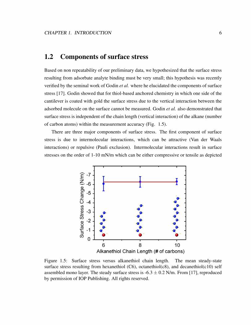
of carbon atoms) within the measurement accuracy (Fig. 1.5).
There are three major components of surface stress. The first component of surface
stress is due to intermolecular interactions, which can be attractive (Van der Waals
interactions) or repulsive (Pauli exclusion). Intermolecular interactions result in surface
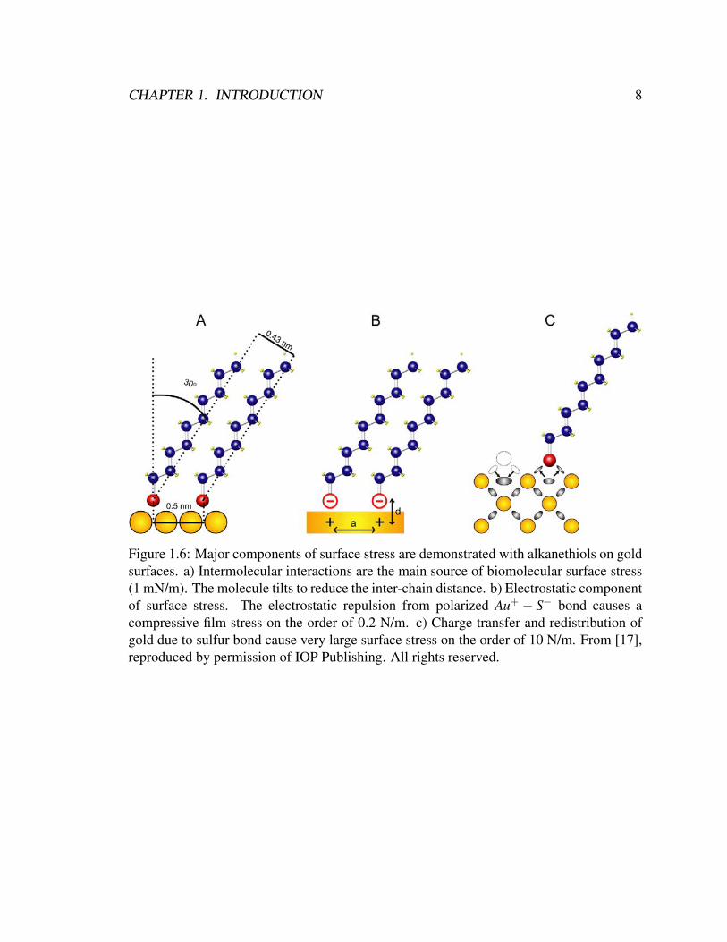
stresses on the order of 1-10 mN/m which can be either compressive or tensile as depicted
Figure 1.5: Surface stress versus alkanethiol chain length. The mean steady-statesurface stress resulting from hexanethiol (C6), octanethiol(c8), and decanethiol(c10) selfassembled mono layer. The steady surface stress is -6.3± 0.2 N/m. From [17], reproducedby permission of IOP Publishing. All rights reserved.

CHAPTER 1. INTRODUCTION 7
in Figure 1.6a. The intermolecular interaction is the main surface stress for biomolecular
sensing application. Unfortunately, it results in the lowest magnitude of surface stress,
therefore cantilevers capturing this type of interactions are operated at their lowest levels
of signal to noise ratio.
The second major component of surface stress is electrostatic interaction. Gold and
sulfur form a covalent bond. However, sulfur (S) is more electronegative (2.58). Therefore
sulfur has a higher tendency to keep electrons, gold has lower electronegativity (2.54)
therefore Au+− S− bond is polarized with slightly negative charge on the sulfur and a
slightly positive charge on the gold as depicted in Figure 1.6b. The same polarity charges
repel each other causing the surface to expand. From the point view of the film, it exhibits a
concave shape or a compressive film stress. The magnitude of the electrostatic components
of surface stress is approximately 0.01-0.1 N/m which depends on packing density.
The third major component of surface stress is surface charge transfer and redistri-
bution, which provides the largest magnitude of surface stress. When a bond is cleaved
at a gold surface, the bulk atoms experience different charge density than the surface
atoms, the surface atoms redistribute their charge (Fig. 1.6c). The loss of the bonds at
the newly formed surface triggers a charge redistribution that results in increased charge
density between the top surface atoms. In case of the gold, the tensile surface stress is
large enough to initiate surface reconstruction [20]. The magnitude of surface stress due to
surface charge transfer and redistribution is on the order of 1-10 N/m.
CHAPTER 1. INTRODUCTION 8
Figure 1.6: Major components of surface stress are demonstrated with alkanethiols on goldsurfaces. a) Intermolecular interactions are the main source of biomolecular surface stress(1 mN/m). The molecule tilts to reduce the inter-chain distance. b) Electrostatic componentof surface stress. The electrostatic repulsion from polarized Au+ − S− bond causes acompressive film stress on the order of 0.2 N/m. c) Charge transfer and redistribution ofgold due to sulfur bond cause very large surface stress on the order of 10 N/m. From [17],reproduced by permission of IOP Publishing. All rights reserved.

CHAPTER 1. INTRODUCTION 9
1.3 Measurement of surface stress
In 1909 Stoney published his seminal paper reporting that a metal film deposited on one
side of a thick substrate was in a state of tension or compression without any external load,
and that it consequently bent the substrate. He deposited 5.6 µm nickel to a 0.31 mm thick,
102 mm long x 12 mm wide ruler [27]. He correctly predicted the radius of curvature of
the rectangular plate with Equation 1.3, with the assumption that the film is much thinner
than the substrate. The modified Stoney’s equation for a rectangular cantilever beam given
by Equation 1.4 uses the biaxial Young’s modulus [28].
σ f ∗ t f =Es ∗ t2
s6∗R
(1.3)
∆y = 3σ f
E∗(lsts)2 (1.4)
Here σ f is the film or surface stress, R is the radius of curvature of the substrate, t f is
the thickness of the film, ls, ts are the length, and thickness of the cantilever, ∆y is the tip
deflection of the cantilever, Es,E∗ are the substrate uniaxial and biaxial Young’s moduli
respectively.
1.4 State-of-the-art-solution
The state of the art solution for measurement of surface stress due to analyte binding uses
two cantilevers. One cantilever is used as a reference and is not functionalized, while the
other, is functionalized with the adsorbate molecule (Fig. 1.7). Only one side of each
cantilever is coated with gold; thiol chemistry is mainly used to attach the adsorbate to
the sensing cantilever [19, 29, 30]. The magnitude of the surface stress for biomolecular
interactions are in the order of 1 mN/m while the charge transfer of sulfur gold bond
generates surface stress in the order of 10 N/m. Therefore a common mode signal which
is 10,000 times larger than the signal (80 dB) needs to be rejected. Since the signals are
subtracted electronically, any time delay or noise that is not common to both cantilevers at

CHAPTER 1. INTRODUCTION 10
Position sensitive
photodetector
Light
Source
Ref
Sens
Figure 1.7: State of the art cantilever design for chemical sensing. Two cantilevers areused, one as a reference and the other as sensing cantilever with different functionalization.The outputs are subtracted to measure the change in deflection due to analyte adsorbatebinding by the sensing cantilever [19].
the same exact time will be interpreted as signal.
In addition to the huge common mode issue, the temperature coefficient of expansion of
gold and silicon is a major issue. The thermal coefficients of expansion for gold and silicon
are 14 ppm/C and 2.6 ppm/C , respectively. Therefore, a small change in temperature
will cause large tip deflections for both the sensing and reference cantilevers (Table 1.1).
Temperature-based signal is reduced according to the degree to which the cantilevers are
matched. However, temperature signal will be misinterpreted as sensing signal in the
presence of cantilever mismatch or a small time lag between the cantilevers. Whenever
a system relies on the subtraction of two large numbers, the fluctuation of large numbers
Surface stress Tip deflection ∆C0.001 N/m 3.38 nm 0.03 C0.1 N/m 334 nm 2.76 C10 N/m 33.4 µm 276 C
Table 1.1: Tip deflection versus surface stress. ∆C indicates temperature change from 25C that will generate the same surface stress or tip deflection as the signal of interest for acantilever that is 100 µm wide, 500 µm long, and 1 µm thick, and has 25 nm thick goldcoating (Chapter 4.1).

CHAPTER 1. INTRODUCTION 11
critically impacts the reliability of the method.
To gain a better understanding of the magnitude of tip deflection involved we will
use equation 1.4. As a model structure we will use a 500 µm long 100 µm wide and 1
µm thick cantilever with 25 nm of gold deposited on the top surface. These cantilevers
are commercially available from Nanoworld USA. However, their thickness should be
measured, since it varies±50%. For all our experiments the cantilever calibration constants
were obtained from thermo-mechanical noise as outlined in Chapter 5 [31]. Table 1.1
shows the magnitude of tip deflection for the three ranges of surface stress. The thermal
expansion rate of gold is higher than silicon, hence it expands at a faster rate than silicon
and bends the cantilever tip down. From Table 1.1 we see for about 0.03C temperature
change the tip deflects 3.3 nm, which corresponds to a surface stress of 1 mN/m. For most
biomolecular application 1 mN/m is the maximum signal resulting from adsorbate analyte
binding. Based on Table 1.1 to measure biomolecular interaction with one percent accuracy
the system must maintain temperature stability of 0.0003 C. Such temperature stability is
not practical, and an alternative solution is needed.
1.5 Innovation
Reproducibility and signal to noise are two major issues that need to be addressed in
performing high sensitivity surface stress measurement. The most important issue effecting
reproducibility is gold. We propose removal of gold. The second major issue is the ability
to measure small surface stress signals on the order of 100 µN/m. We propose taking
advantage of narrow sub Hertz bandwidth of the chemical signal and moving it away from
the low frequency drift. Also combining the reference and sensing cantilever into one
gives the added benefit of common mode noise rejection. By eliminating gold we improve
reproducibility and repeatability. Gold grain structure and morphology has significant
impact in reproducibility of the result. Godin [17] shows surface stress is independent of
Alakanethiol chain length while Berger [18] shows that surface stress is Alkanethiol chain
length dependent. The discrepancy stems from the gold grain size, sulfur absorbtion and
heavily pitted gold surface. [32] We also propose combining the reference and the signal
cantilever into one. Taking advantage of the inherent natural subtraction of top surface

CHAPTER 1. INTRODUCTION 12
Σ
XBinding to
selective
coating
Tip
Deflection
Time
V
Voltage
Surface
Charge
Innovation
Liquid
Noise
Surface
Stress
Temperature
Cantilever AFM
Light on/off at F0
Rate
Figure 1.8: Architecture of the proposed single-cantilever system. The architectureresembles a lock-in amplifier, where the desired surface stress is modulated at a specificfrequency in order to distinguish it from background noise.
stress from the bottom surface stress which results in tip deflection. Subtraction of the
reference cantilever from the signal cantilever is done mechanically. Time lags do not
play important role since there is only one cantilever. The draw back to this technique is
the added complexity of different top and bottom cantilever surface functionalization. A
fundamental solution shown in Figure 1.8 is to make the desired surface stress time varying
at a specific frequency above the drift, and to observe the output at that specific frequency.
Then the other undesired effects such as temperature or the 1/f noise would not matter since
they would fall outside the band of the detection. A molecule that changes its shape due to
light is needed. By shining light on and off at a specific rate we can modulate the surface

CHAPTER 1. INTRODUCTION 13
stress at a specific frequency.
We propose modulating the cantilever surface stress signal over time using an azo dye in
order to spectrally separate the sensor signal from the background noise as shown in Figure
1.8. The physical behaviors of azo dyes are based on the isomerization of constituent
molecules, which undergo a large conformational change from one state to another in
response to the absorption of light at distinct wavelengths. The light-induced transition
of azobenzene derivatives (C6H5N=NC6H5) between the extended (trans) and compact
(cis) configuration gives rise to changes in molecular polarity, dipole moment, and shape.
Most azobenzene-based thin films are fabricated into materials such as polymers, liquid
crystals, Langmuir-Blodgett films, [33] and physically or chemically adsorbed monolayers
on gold surfaces [34–37]. In practice, photoswitches have been influenced by the density
and orientation of azobenzene-based self-assembled monolayers (SAMs). For example,
an azobenzene-contained alkanethiol self-assembled onto gold substrates exhibited no
response upon UV irradiation due to steric hindrance [38, 39]. The minimum area for
isomerization of azobenzene has been estimated to be 0.4 nm2 [40]. In contrast with
thiol-based SAMs, specific silane-based SAMs provide sufficient room between molecules
to prevent steric hindrance and have been shown as alignment layer for liquid crystal
networks. [41]
1.6 Detection modes
There are two major modes of detection of cantilever surface stress, optical or piezoresis-
tive. Following the development of the scanning tunneling microscope, the atomic force
microscope, and the use of small piezoresistive cantilevers for atomic force microscopy,
there has been increasing interest in the use of MEMS piezoresistors as a read out for
measuring chemical and biosensing variables. [42] Piezoresistive sensors are especially
well suited to this task, because they are small, low power, have a relatively stable DC
response, especially if temperature compensated, and can readily integrated into arrays to
provide a means of separating chemical species based on differential binding affinity for
varying coatings. [43] A silicon piezoresistive sensing element is formed on the surface of
small MEMS silicon cantilevers. A chemically sorptive layer is deposited on the silicon
CHAPTER 1. INTRODUCTION 14
surface. The layer expands or shrinks upon binding and causes the silicon cantilever to
bend causing a change in resistance of the silicon piezoresistor. Stoney’s equation relates
the bending radius of the micro cantilever caused by the stressed layer to the stress in the
piezoresistor.
1.7 Outline
As we move toward Nano Electro Mechanical systems (NEMS), the fields of mechanics
and chemistry merge. In this work we designed a mechanical actuator at molecular
(nano) scale. We then assembled the actuator molecules in a single structured layer
on a pure silicon cantilever. The actuator molecule absorbs a photon of 405 nm and
changes it shape. The change of molecular actuator shape result in expansion of actuator
assembled layer and causes the cantilever to bend. From the tip deflection of the
cantilever and careful measurements that exclude the effects of heating we were able
estimate on average force per molecule of 0.3 pN. The synthesized molecule was (E)-2-
((4-(dimethylamino)phenyl)diazenyl)-N-(3-(triethoxysilyl)propyl)benzamide, and self as-
sembled on hydroxylated silicon surface. [44]
Figure 1.9 gives the overall understanding of this work. It only represents the
experiments that worked. Yet most of the learning process was based on experiments that
did not work, which we have briefly included, and hope to serve as the basis of which path
not to follow.
Being aware that the chemistry is rather involved, we have published the recipe and
given the synthesis recipe to a commercial manufacturer that can provide the actuation
molecule for further investigation by interested researchers (www.medchemsource.com).
In Chapter 2 we search for a molecule that changes it shape with light. We also confront
the challenges of making the molecule. We found azobenzene, as the molecule of choice.
However practical issues of using the molecule prohibited its use. For example an optical
lens that could work at 320 nm was exceedingly expensive and a laser at 320 nm was not
available to us. Therefore, we choose a derivative (Methyl Red) that allowed shape change
at 405 nm. Chapter 2 also covers the synthesis of the azobenzene derivatives that can be

CHAPTER 1. INTRODUCTION 15
Figure 1.9: Overview of the work. A pure silicon bulk micromachined cantilever wascoated with an actuator molecule that caused tip motion, when excited by 405nm laser.Reprinted with permission from [44]. Copyright 2013 American Chemical Society.
attached to cantilever.
In Chapter 3 we discuss the self assembly and the techniques used to deposit and
characterize a monolayer. The issue of polymerization and surface preparation are
discussed in depth.
In Chapter 4 we explore different modes of transduction. By transduction we mean
conversion of the surface stress to an electrical response. We look at piezoresistive sensors
and explore how to lower their flicker noise. We also explore the design issues and the
differences between force loaded cantilevers and surface stress optimized cantilevers. In
Chapter 4 we also discuss calibration and the pertinent equations.
In Chapter 5 we discuss key aspects of measurements. We look at different noise
sources and provide a path to their minimization. The signal processing needed to pull
the signal from the noise is also discussed in depth.
In Chapter 6 we outline a new technique we refer to as a two tone test. The two tone test
provides a basis for measuring the curvature of a cantilever and has the potential to elucidate
direct intermolecular interactions. This method of measurement with further investigation
has the potential to unravel the components of surface stress.

Chapter 2
Photochemistry
We first set out to find a molecule that changes its shape due to light. We looked at nature
to see where it uses a molecule with large conformational change. Interestingly, our vision
is based on large conformational changes of retinal molecules. This molecule commonly
known as vitamin A is shown in Figure 2.1. The cis-Retinal molecule fits in a tight pocket
of a protein called opsin. Upon absorbing a visible photon cis-Retinal changes its shape
to trans-Retinal, so that it no longer fits in the pocket [45]. The shape change in the opsin
protein eventually leads into an electrical action potential impulse which we perceive as
vision [46].
The choices of available compounds are shown in Figure 2.2. Our first choice was
retinal, however due the difficulty of handling and isomerization we chose a different
molecule. Azobenzene was chosen due to its availability, wide industrial use, clean
O
O
Retinal isomerase
Visible photon
cis-Retinal trans-Retinal
Figure 2.1: Retinal molecule. The molecule changes its shape due to absorption of light.
16
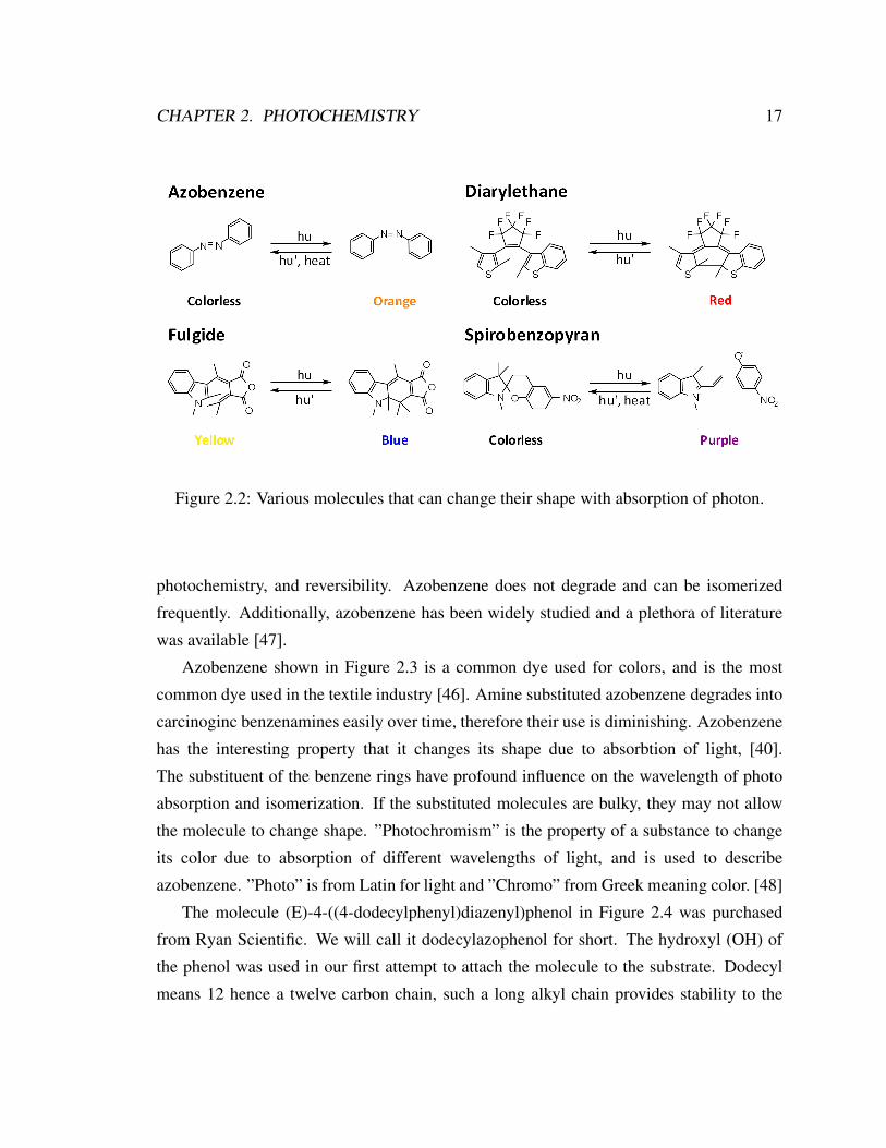
CHAPTER 2. PHOTOCHEMISTRY 17
Figure 2.2: Various molecules that can change their shape with absorption of photon.
photochemistry, and reversibility. Azobenzene does not degrade and can be isomerized
frequently. Additionally, azobenzene has been widely studied and a plethora of literature
was available [47].
Azobenzene shown in Figure 2.3 is a common dye used for colors, and is the most
common dye used in the textile industry [46]. Amine substituted azobenzene degrades into
carcinoginc benzenamines easily over time, therefore their use is diminishing. Azobenzene
has the interesting property that it changes its shape due to absorbtion of light, [40].
The substituent of the benzene rings have profound influence on the wavelength of photo
absorption and isomerization. If the substituted molecules are bulky, they may not allow
the molecule to change shape. ”Photochromism” is the property of a substance to change
its color due to absorption of different wavelengths of light, and is used to describe
azobenzene. ”Photo” is from Latin for light and ”Chromo” from Greek meaning color. [48]
The molecule (E)-4-((4-dodecylphenyl)diazenyl)phenol in Figure 2.4 was purchased
from Ryan Scientific. We will call it dodecylazophenol for short. The hydroxyl (OH) of
the phenol was used in our first attempt to attach the molecule to the substrate. Dodecyl
means 12 hence a twelve carbon chain, such a long alkyl chain provides stability to the

CHAPTER 2. PHOTOCHEMISTRY 18
NN
Azo Function
Benzene
NN
UV 365 nm Light
Heat, blue light 475 nm
Trans configuration Cis configuration
Figure 2.3: Azobenzene molecule is photochromatic, and changes its shape due toabsorption of light at different wavelengths.
molecule configuration. The benzene with the OH attached to it is called phenol and is a
carcinogen by itself. Our attempt was to use the Williamson ether synthesis [46, pg. 349]
for attachment of this molecule to the substrate. The substrate was first coated with 11-
bromoundecyltrimethoxy silane. We expected the OH of the phenol would displace the
bromine with a SN2 reaction mechanism and attach, however the oxygen in such a highly
conjugated system is not a good nucleophile and after many attempts we abandoned this
approach [49].
2.1 Absorbance
The major goals of synthesis were to make a molecule that allowed the attachment of the
azobenzene to the substrate, and that the attachment molecule would not hinder the activity
of azobenzene molecule. Azobenzene by itself did not attach to silicon or gold substrate, it
only physisorbed. Absorbance of derivative azobenzene molecule in liquid was the first step
in qualification of successful synthesis. Our first strategy was to attach a well characterized
optically inactive base layer to silicon and use a derivative azobenzene molecule to attach
to the base layer. The absorbance spectra of the dodecylazophenol molecule is shown in
Figure 2.5. The UV exposure was taken with a 4 Watt ultra violet lamp (UV) and the

CHAPTER 2. PHOTOCHEMISTRY 19
OH
NN
OH
NN
(E)-4-((4-dodecylphenyl)diazenyl)phenolChemical Formula: C48H68N4O2
Exact Mass: 732.5Molecular Weight: 733.1
m/z: 732.5 (100.0%), 733.5 (54.3%), 734.5 (14.8%), 735.5 (2.7%)Elemental Analysis: C, 78.64; H, 9.35; N, 7.64; O, 4.36
Figure 2.4: We call this molecule dodecylazophenol for short. The long alkyl (12 carbon)chain provides stability for the switching of molecule.
primary purpose was to see the trends rather than actual quantitative measurement, such as
rate constant, etc. As expected when the molecule is exposed to UV (340 nm) it switches
its configuration from trans to cis, hence there are lower numbers of molecule in trans state
that can absorb the UV light hence lower absorbance in the UV region. When the molecule
is exposed to blue light or just left alone for few days in the dark at room temperature the
cis molecules revert back to trans and the absorbance equals the original absorbance, this
reversibility is the hallmark of photo switching. There are other molecules that upon UV
radiation change their absorbance; however they are not reversible, which usually means
disintegration, also the main reason that colors fade under sunlight.
The vertical axis of the graph is absorbance, according to Beer-Lambert Law the
absorption is A = ε ∗ l ∗ c , where ε is the extinction coefficient, l is the path length
in centimeters and is normally 1 cm for most cuvettes, and c is the concentration. By
measuring the absorbance, the concentration can be determined. It is important to note this
law is valid over several decades of concentrations, however at high concentration it tends
to break down due to aggregation of molecules. The absorbance can also be written as
log(I/I0), where I is the measured intensity from the solution and I0 is intensity measured
from the reference solvent. Absorption measure of 1 means the measured light is 10 times

CHAPTER 2. PHOTOCHEMISTRY 20
lower intensity than the reference and absorption of 2 means the light is 100 times lower
intensity. Absorbance is usually positive since the intensity of the light through the solution
is lower than the solvent, the negative sign in front of the equation above makes log(x)
positive where x is less than 1.
The absorption in the UV region of the spectrum for an organic molecule is due to
excitation of an electron from π orbital to π∗ orbital. In order for a molecule to absorb UV
the π electron in the highest occupied molecular orbital (HOMO) needs to jump to π∗ which
is the lowest un-occupied molecular orbital (LUMO). For example hexane does not have
any double bonds so it will not absorb a photon in UV region, but acetone has an oxygen
double bonded to carbon so it will have a absorption in UV [50]. For a molecule to absorb
light an electron has to be excited; according to the Stark-Einstein law a molecule only
absorbs light to bring about a single transition, and the energy of the photon must match
between the ground state and some excited state [51]. The η to π∗ transition state is of
lower energy hence longer wavelength. The η - π∗ is due to nitrogen lone pair being excited
to the higher energy π∗ state. The cis-azobenzene molecule upon absorption of photon of
η - π∗ energy will change its shape to trans-azobenzene. Hence upon UV radiation the
300 320 340 360 380 400 420 440 460 480 5000
0.5
1
1.5
2
Wavelength in nm
Abs
orba
nce
1 minute UV exposure
η − π *
π−π* 3 minute UV Exposure
no UV exposure
Figure 2.5: Absorbance of dodecylazophenol. The strong absorption in the UV region isdue to molecules in trans configuration. When the molecules were placed in dark theyreverted to their original absorbance (not shown for clarity).
CHAPTER 2. PHOTOCHEMISTRY 21
population of the the trans-azobenzene molecules diminishes and population of the cis-
azobenzene molecules increases [52].
To completely understand the details of electronic orbitals we need to solve the quantum
mechanical (Schrodinger) equation; however instead orbital molecular theory helps to gain
an intuitive understanding of the molecular system. The energy of light in electron volts is
given by E(ev) = 1240ev−nmλ (nm) . Hence a photon at 365 nm wavelength has an energy of 3.6
ev. The π −π∗ strong absorption of azobenze is due to its high quantum efficiency [53],
in fact the molecular absorption coefficient of Methyl red, an azobenzene, derivative is
ε = 27,660 dm3/(mol ∗ cm) [54]. The substituent on the benzene ring of azobenzene has
pronounced effect on the absorption spectra.
The wide variety of azobenzene chromophores display a wide range of properties
depending on the ring substituent. Two of the molecules that we synthesized are shown
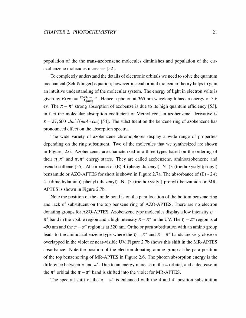
in Figure 2.6. Azobenzenes are characterized into three types based on the ordering of
their η ,π∗ and π,π∗ energy states. They are called azobenzene, aminoazobenzene and
pseudo stilbene [55]. Absorbance of (E)-4-(phenyldiazenyl) -N- (3-(triethoxysilyl)propyl)
benzamide or AZO-APTES for short is shown in Figure 2.7a. The absorbance of (E) - 2-((
4- (dimethylamino) phenyl) diazenyl) -N- (3-(triethoxysilyl) propyl) benzamide or MR-
APTES is shown in Figure 2.7b.
Note the position of the amide bond is on the para location of the bottom benzene ring
and lack of substituent on the top benzene ring of AZO-APTES. There are no electron
donating groups for AZO-APTES. Azobenzene type molecules display a low intensity η−π∗ band in the visible region and a high intensity π−π∗ in the UV. The η−π∗ region is at
450 nm and the π−π∗ region is at 320 nm. Ortho or para substitution with an amino group
leads to the aminoazobenzene type where the η −π∗ and π −π∗ bands are very close or
overlapped in the violet or near-visible UV. Figure 2.7b shows this shift in the MR-APTES
absorbance. Note the position of the electron donating amine group at the para position
of the top benzene ring of MR-APTES in Figure 2.6. The photon absorption energy is the
difference between π and π∗. Due to an energy increase in the π orbital, and a decrease in
the π∗ orbital the π−π∗ band is shifted into the violet for MR-APTES.
The spectral shift of the π − π∗ is enhanced with the 4 and 4’ position substitution

CHAPTER 2. PHOTOCHEMISTRY 22
NN
O NH
SiO
O
O
NN
O NH
SiO
O
O
N
(E)-4-(phenyldiazenyl)-N-(3-(triethoxysilyl)propyl)benzamideChemical Formula: C22H31N3O4Si
Exact Mass: 429.2
(E)-2-((4-(dimethylamino)phenyl)diazenyl)-N-(3-(triethoxysilyl)propyl)benzamide
Chemical Formula: C24H36N4O4SiExact Mass: 472.3
AZO-APTES MR-APTES
Figure 2.6: AZO-APTES and MR-APTES molecule for short.
of benzene rings with electron-donor and electron-acceptor (push/pull) substituent in the
pseudo-stilbene class of compounds. The π−π∗ band is shifted to the red, past that of the
η −π∗ to assume a reverse order. Cis to trans thermal isomerization can range from the
order of hours and days for azobenzenes to seconds and milliseconds for pseudo-stilbenes
[56]. The ability to change the absorbance spectra of azobenzene is of significant practical
importance. For example in our case due to lack of availability of 320 nm laser we could
not continue the experiments; however by using the MR-APTES the spectrum shifted to
where an available 405 nm could be employed.

CHAPTER 2. PHOTOCHEMISTRY 23
a)
b)
Figure 2.7: AZO-APTES and MR-APTES absorbance. a) AZO-APTES absorbance greenand orange traces are absorbance after exposure to UV light. b)MR-APTES absorbance,orange and green traces are absorbance after 5, and 10 second exposure to 405 nm laser.Both materials were dissolved in anhydrous toluene.

CHAPTER 2. PHOTOCHEMISTRY 24
2.2 Synthesis
The goals of synthesis were to make a molecule that 1) allows the attachment of the
azobenzene to the substrate, 2) allows enough space for the molecule to isomerize once
bound to substrate, and 3) allows for formation of the self assembled mono layer [37]. The
choice of substrate was very important since it dictated how the synthesis should proceed.
We had three choice of substrate: gold, silicon, and native silicon dioxide. Substrate for
us meant silicon cantilevers which we fabricated or purchased. First we started with gold
deposited on silicon cantilevers, hence a gold substrate and thiol chemistry [57]. Sulfur and
gold form excellent mono layer due to electron transfer from gold to sulfur [34]. The sulfur
gold bond is commonly used to form self-assembled monolayer (SAM) [36]. However,
photoswitchs have been influenced by the density and orientation of such azobenzene-
based SAM [35], [58]. If the free area of azobenzene photoswitch is less than 0.41 nm2
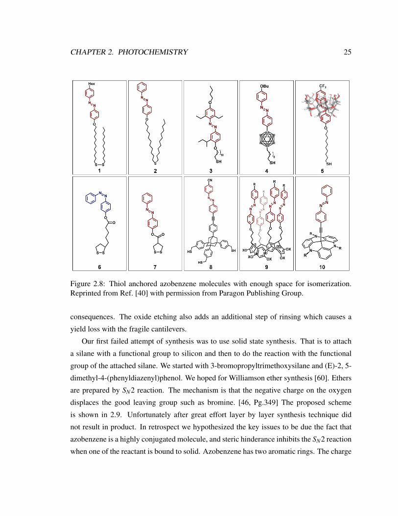
isomerization does not take place. Figure 2.8 shows different schemes used to make thiol
anchored azobenzene molecules to ensure free volume for isomerization once bound to
gold substrate [40]. We also found gold on silicon cantilevers is not a good choice due to
thermal issues detailed in Chapter 4.
The road to synthesis was rather difficult, many times we had to go back and try new
material. Also access to proper equipment and availability was a major issue. So we opted
for the most simple and reliable synthesis within our capability. All of the synthesis was
done under the fume hood. In retrospect the major lessons learned were:
• start with low cost starting material
• do not allow any material with greater than health hazard 2
• keep the reaction conditions mild and limited to room temperature.
Our second choice of pure silicon substrate was not practical in our setting. Silicon
forms a native oxide under room temperature. In order to remove this native oxide the
cantilevers must be etched with either ammonium fluoride or hydrofluoric acid [59]. These
acids can not be stored in glass, and a possible mix up in waste disposal may have disastrous
CHAPTER 2. PHOTOCHEMISTRY 25
Figure 2.8: Thiol anchored azobenzene molecules with enough space for isomerization.Reprinted from Ref. [40] with permission from Paragon Publishing Group.
consequences. The oxide etching also adds an additional step of rinsing which causes a
yield loss with the fragile cantilevers.
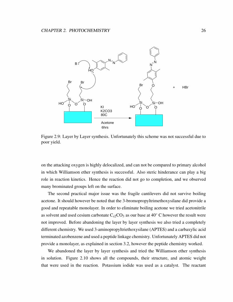
Our first failed attempt of synthesis was to use solid state synthesis. That is to attach
a silane with a functional group to silicon and then to do the reaction with the functional
group of the attached silane. We started with 3-bromopropyltrimethoxysilane and (E)-2, 5-
dimethyl-4-(phenyldiazenyl)phenol. We hoped for Williamson ether synthesis [60]. Ethers
are prepared by SN2 reaction. The mechanism is that the negative charge on the oxygen
displaces the good leaving group such as bromine. [46, Pg.349] The proposed scheme
is shown in 2.9. Unfortunately after great effort layer by layer synthesis technique did
not result in product. In retrospect we hypothesized the key issues to be due the fact that
azobenzene is a highly conjugated molecule, and steric hinderance inhibits the SN2 reaction
when one of the reactant is bound to solid. Azobenzene has two aromatic rings. The charge
CHAPTER 2. PHOTOCHEMISTRY 26
SiHO O O
Br
SiO
OH
Br
NN
HO
KIK2CO380C
Acetone
SiHO O O
Br
SiO
O
OH
B NN
6hrs
+ HBr
Figure 2.9: Layer by Layer synthesis. Unfortunately this scheme was not successful due topoor yield.
on the attacking oxygen is highly delocalized, and can not be compared to primary alcohol
in which Williamson ether synthesis is successful. Also steric hinderance can play a big
role in reaction kinetics. Hence the reaction did not go to completion, and we observed
many brominated groups left on the surface.
The second practical major issue was the fragile cantilevers did not survive boiling
acetone. It should however be noted that the 3-bromopropyltrimethoxysilane did provide a
good and repeatable monolayer. In order to eliminate boiling acetone we tried acetonitrile
as solvent and used cesium carbonate Cs2CO3 as our base at 40 C however the result were
not improved. Before abandoning the layer by layer synthesis we also tried a completely
different chemistry. We used 3-aminopropyltriethoxysilane (APTES) and a carbaxylic acid
terminated azobenzene and used a peptide linkage chemistry. Unfortunately APTES did not
provide a monolayer, as explained in section 3.2, however the peptide chemistry worked.
We abandoned the layer by layer synthesis and tried the Williamson ether synthesis
in solution. Figure 2.10 shows all the compounds, their structure, and atomic weight
that were used in the reaction. Potassium iodide was used as a catalyst. The reactant

CHAPTER 2. PHOTOCHEMISTRY 27
concentrations were at 0.25M, and the catalyst potassium iodide at 0.01M. Figure 2.11
shows the the total positive electrospray current coming off of the liquid chromatograph
column. The chromatograph separates the compounds in time. The mass spec then provides
the mass of each time separated compound. The detail of liquid chromatography and mass
spectrometry (LC/MS) are given in appendix C.
Figure 2.12 shows the mass of separated component of column in each time portion.
Since the mass of the particles must be charged (ions) the atomic weight of each ion for
positive electrospray has a additional mass of (1) for hydrogen or additional mass +23 for
sodium (Na). The horizontal axis is the atomic mass and the vertical axis the ion current.
Note the appearance of partially hydrolyzed product in the middle graph. The mass of the
hydrolyzed and ionized product found in the middle graph is 375.2 amu.
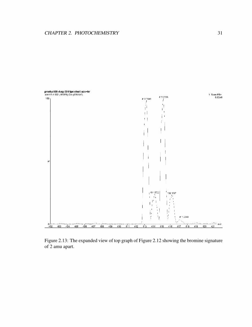
In mass spectrometry brominated compounds have a distinct signature which is rather
easy to identify. Bromine has a molecular weight of 79 atomic mass unit (amu) and
its isotope a mass of 81 amu with the same abundance, hence a ratio of 1:1 is always
found. A brominated compound will show as two peaks of identical amplitude that are
2 atomic mass unit apart. As an example top graph of Figure 2.12 shows this signature.
The zoomed view of the this graph is shown in Figure 2.13 which we hypothesize to
be partially polymerized 3-bromopropyltrimethoxysilane. We had similar result with
dodecylazophenol shown in Figure 2.4. Unfortunately the starting material for the synthesis
were extremely expensive. The (E)-2, 5-dimethyl-4-(phenyldiazenyl)phenol was about
8000 USD/g from sigma aldrich, and dodecyl azo phenol was 160 USD/10 mg or 16,000
USD/g from Ryan scientific, Mt Pleasent, SC. Since we needed to purify the product,
optimize the reaction, and had issues with polymerization of product, we decided not to
pursue this reaction after the sixth try.

CHAPTER 2. PHOTOCHEMISTRY 28
K+ I-
potassium iodideChemical Formula: IK
Exact Mass: 165.9Molecular Weight: 166.0
m/z: 165.9 (100.0%), 167.9 (7.2%)Elemental Analysis: I, 76.45; K, 23.55
NN
HO
(E)-2,5-dimethyl-4-(phenyldiazenyl)phenolChemical Formula: C14H14N2O
Exact Mass: 226.1
Si
NN
O
Si
O
OBr
(3-bromopropyl)trimethoxysilaneChemical Formula: C6H15BrO3Si
Exact Mass: 242.0Molecular Weight: 243.2
Cs+Cs+-O
O
O-
cesium carbonateChemical Formula: CCs2O3
Exact Mass: 325.8
N
Chemical Formula: C2H3NExact Mass: 41.0
O
O
(E)-1-(2,5-dimethyl-4-(3-(trimethoxysilyl)propoxy)phenyl)-2-phenyldiazeneChemical Formula: C20H28N2O4Si
Exact Mass: 388.2Molecular Weight: 388.5
m/z: 388.2 (100.0%), 389.2 (27.9%), 390.2 (7.8%), 391.2 (1.3%)
O
Si
NN
OO
O
(E)-(3-(2,5-dimethyl-4-(phenyldiazenyl)phenoxy)propyl)dimethoxysilanolChemical Formula: C19H26N2O4Si
Exact Mass: 374.2Molecular Weight: 374.5
m/z: 374.2 (100.0%), 375.2 (26.8%), 376.2 (7.5%), 377.2 (1.2%)
Cs2Co3KIACN24hr 40C
+
Acetonitrile
OH
O
Figure 2.10: Williamson ether synthesis. All components of the reaction with theiratomic weight, which were monitored in mass spectrometry. The product and a partiallyhydrolyzed product are also shown.

CHAPTER 2. PHOTOCHEMISTRY 29
Figure 2.11: Total positive electrospray ion current (TIC) from the crude product of theWilliamson ether synthesis. The horizontal axis is time in minutes, and the vertical axistotal positive ion current. The crude product solution is separated in time in the liquidcolumn chromatograph.

CHAPTER 2. PHOTOCHEMISTRY 30
Figure 2.12: The ion mass found at different column time: Top, ion mass at 19.8 minutes,middle ion mass at 17.8 minute which contains partially hydrolyzed product, and bottomion mass at 15.2 minute.
CHAPTER 2. PHOTOCHEMISTRY 31
Figure 2.13: The expanded view of top graph of Figure 2.12 showing the bromine signatureof 2 amu apart.

CHAPTER 2. PHOTOCHEMISTRY 32
2.3 Peptide linkage chemistry
In order to achieve a chemistry that was practical we looked at the most commercially
available and cost sensitive chemistry, peptide linkage chemistry. The reactants work at
room temperature, are commercially available and convert the reaction to completion with
high yield.
Peptide linkage is chemistry of attachment of the a carboxylic acid of one amino acid to
the amine group of the other, the amide linkage joining the amino acids is called the peptide
bond. Carboxylic acid is a stable molecule due its resonance structure and will not react
with and amine directly. There are several method for activation of the carboxylic acid,
however, each method presents challenges in purification, hydrolysis, and stability. [61]
The goal is to attach the azobenzene molecule to the surface of silicon. The attachment
to silicon is done through silane chemistry and is covered in the Chapter 3. Here the
attachment of azobenzene to silane is described.
Our first several attempts was the reaction of 4-(phenyl diazneyl) benzoic acid and 3-
aminopropyltrimethoxysilane as shown in Figure 2.14. The reaction steps are also provided
in the same figure. The 4-(phenyl diazneyl) benzoic acid was purchased from sigma aldrich
at cost of 25 USD/g and used as received. The 3-aminopropyltrimethoxysilane was also
purchased from sigma aldrich at cost of 85 USD/100 ml. Even thought the synthesis was
successful and product was obtained, the product was not stable, it would precipitate out of
the eluted solvent in matter of minutes to hours depending on the day.
To solve the mystery of the product disappearance we re-traced every step since
at the time we did not know if the issue was due to the synthesis condition, re-
actants, or some other unknown variable such as air moisture. We used Nuclear
magnetic resonance to investigate the reaction and the reactants, and as in any puz-
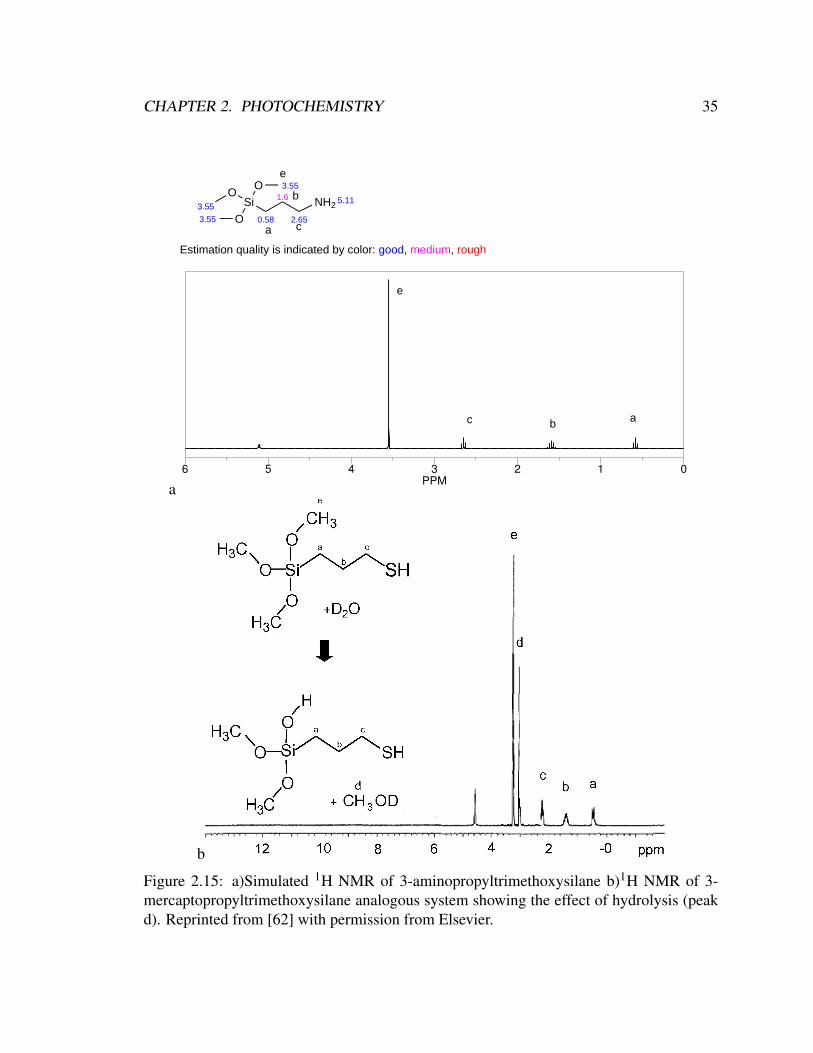
zle once solved it became obvious. Scott et al. [62] investigated the influence of
bath chemistry on 3-mercaptoporpytrimethoxysilane. Figure 2.15a shows a simulated
NMR of 3-aminopropylmethoxysilane and Figure 2.15b the analogous system of 3-
mercaptoporpytrimethoxysilane from Scott et al. Peak a, b, c can be used as internal
reference and are not affected by hydrolysis. Note that peak d does not appear in the
simulated NMR since hydrolysis was not simulated. Peak d was due to hydrolysis. From
CHAPTER 2. PHOTOCHEMISTRY 33
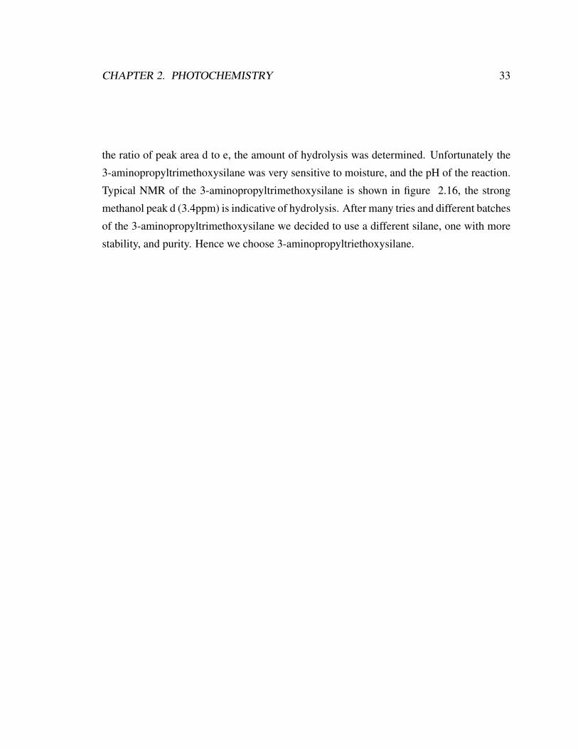
the ratio of peak area d to e, the amount of hydrolysis was determined. Unfortunately the
3-aminopropyltrimethoxysilane was very sensitive to moisture, and the pH of the reaction.
Typical NMR of the 3-aminopropyltrimethoxysilane is shown in figure 2.16, the strong
methanol peak d (3.4ppm) is indicative of hydrolysis. After many tries and different batches
of the 3-aminopropyltrimethoxysilane we decided to use a different silane, one with more
stability, and purity. Hence we choose 3-aminopropyltriethoxysilane.

CHAPTER 2. PHOTOCHEMISTRY 34
NH2Si
OO
O
3-(trimethoxysilyl)propan-1-amineExact Mass: 179.1
O
OH
NN
(E)-4-(phenyldiazenyl)benzoic acidExact Mass: 226.1
NSi
O
NN
H
(E)-4-(phenyldiazenyl)-N-(3-(trimethoxysilyl)propyl)benzamideExact Mass: 387.2
N
NO+
NN
N
N P-
F
FF
F
FF
2-(3H-[1,2,3]triazolo[4,5-b]pyridin-3-yl)-1,1,3,3-tetramethyluronium hexafluorophosphate(V)
Exact Mass: 380.1
N
acetonitrileExact Mass: 41.0
1. Dissolve 226mg of azenyl Benzoic Acid in 3ml of Acetonitrile and 90ul of triethyl amine (1.2eq)(density .722) 2. add 456mg of HATU to solution (1.2eq).
4. ADD 215ul (1.2eq) of 3-aminoTrimethoxy silane
5.Stirr for 1 hour.
6. Evaporate the ACN
7.Purify using silica gel 50% Hexane to ethylacetate
O
O
NN
1,1,3,3-tetramethylureaExact Mass: 116.1
OO
OH
Exact Mass: 32.0
NN
N
N
HAOtExact Mass: 136.0
N
Exact Mass: 101.1
PRODUCT
OH
TriethylAmineDensity .72
P-
F
FF
F
FF
hexafluorophosphate(V)Exact Mass: 145.0
HATU
+
HATUACN
Figure 2.14: 4-(phenyldiazneyl)benzoic acid reaction with 3-aminopropyltrimethoxysilane.
CHAPTER 2. PHOTOCHEMISTRY 35
a
5.11
3.55
3.55
3.55 0.58
1.6
2.65
NH2Si
OO
O
Estimation quality is indicated by color: good, medium, rough
e
ca
b
abc
e
b
Figure 2.15: a)Simulated 1H NMR of 3-aminopropyltrimethoxysilane b)1H NMR of 3-mercaptopropyltrimethoxysilane analogous system showing the effect of hydrolysis (peakd). Reprinted from [62] with permission from Elsevier.

CHAPTER 2. PHOTOCHEMISTRY 36
Figure 2.16: Hydrolysis indication of 3-aminopropyltrimethoxysilane. 1H NMR of 3-aminopropyltrimethoxysilane in deuterated methanol showing hydrolysis.

Chapter 3
Self Assembled Monolayer - SAM
Self-assembled monolayers are molecular assemblies that are formed spontaneously by
exposure of an appropriate substrate to a solution of an active surfactant in an organic
solvent. Figure 3.1 shows the forces for self assembly. The chemisorption to the surface
brings molecules close together, which allows the short range forces (i.e. Van der Waals
forces) to become important. [37] One of the major challenges for our monolayer was
devising the right spacing needed for the azobenzene molecule to switch.
On page 24 the overall approach to synthesis was discussed, and silane chemistry was
chosen. Silicon is under carbon in the periodic table and has similar properties, with one
Figure 3.1: A schematic view of forces in a Self Assembled Monolayer. [63, Pg.238] Withpermission from Academic press.
37
CHAPTER 3. SELF ASSEMBLED MONOLAYER - SAM 38
a)
b)
Figure 3.2: Silane based SAM polymerized due to water on silicon surface. a, b) Visiblewhite layers are polymer islands due to self polymerization.
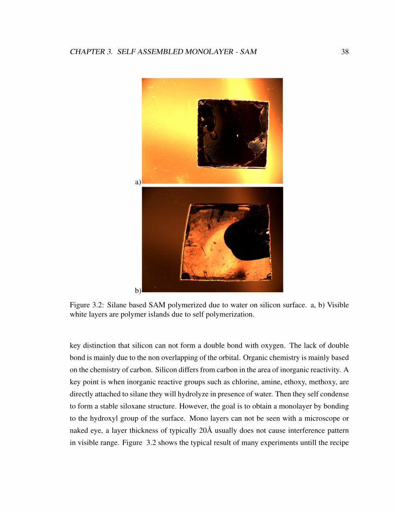
key distinction that silicon can not form a double bond with oxygen. The lack of double
bond is mainly due to the non overlapping of the orbital. Organic chemistry is mainly based
on the chemistry of carbon. Silicon differs from carbon in the area of inorganic reactivity. A
key point is when inorganic reactive groups such as chlorine, amine, ethoxy, methoxy, are
directly attached to silane they will hydrolyze in presence of water. Then they self condense
to form a stable siloxane structure. However, the goal is to obtain a monolayer by bonding
to the hydroxyl group of the surface. Mono layers can not be seen with a microscope or
naked eye, a layer thickness of typically 20A usually does not cause interference pattern
in visible range. Figure 3.2 shows the typical result of many experiments untill the recipe

CHAPTER 3. SELF ASSEMBLED MONOLAYER - SAM 39
a)
b)
Figure 3.3: Silane based SAM polymerized due to water on cantilever. a, b) Cantileversshowed the same polymerization as silicon pieces.
was developed. Figure 3.3 shows the same type of polymerization on cantilevers. When a
silane contains at least one carbon silicon bond it is called an organosilane. The chemical
reactivity of direct silicon-carbon bond is not high if a methyl or higher alkyl is used. The
bond disassociation energy of silicon with methyl group is about 90kcal/mol [64].
Our first approach to making the azobenzene SAM was a two step approach. The idea
follows the Merrifield solid phase synthesis [65]. The simple concept is to bind the silane
molecule with a functional group to silicon substrate first and then run the subsequent
reactions, since the molecule is bound to the substrate the subsequent reactions can be
done several time to achieve high yields. Also attaching the silane to silicon substrate as

CHAPTER 3. SELF ASSEMBLED MONOLAYER - SAM 40
NN
OH
(E)-2,5-dimethyl-4-(phenyldiazenyl)phenolChemical Formula: C14H14N2O
Exact Mass: 226.1
Figure 3.4: 2, 5-dimethyl-4-(phenyldiazenyl)phenol
Si
O
OO
Br
(11-bromoundecyl)trimethoxysilaneChemical Formula: C14H31BrO3Si
Exact Mass: 354.1Molecular Weight: 355.4
m/z: 356.1 (100.0%), 354.1 (96.9%), 357.1 (20.2%), 355.1 (20.1%), 358.1 (5.6%)Elemental Analysis: C, 47.32; H, 8.79; Br, 22.48; O, 13.51; Si, 7.90
Figure 3.5: 11-bromoundecyltrimethoxysilane
the first step was very attractive since the synthesis of the azobenzene would not cause self
polymerization. Unfortunately in practice the yield loss of fragile cantilevers was severe,
as can be seen from the broken cantilevers of Fig. 3.3b.
3.1 11-bromoundcyltrimethoxysilane
The first film that we deposited was 11-bromoundecyltrimethoxysilane. Our intent was to
do solid state Williamson ether synthesis with azobenzene derivative shown in fig 3.4.
To elaborate on the name, 11 stands for the location of the bromine on the carbon chain
(carbon 11). The bromo stands for bromine. Undecyl latin for eleven, and methoxy the
name for one carbon connected to oxygen. Here we have three methoxy group connected
CHAPTER 3. SELF ASSEMBLED MONOLAYER - SAM 41
to the silicon hence trimethoxysilane. Figure 3.5 shows the molecule.
We found the 11-bromoundecyltrimethoxysilane molecule to be stable in air and it
did not readily polymerize in toluene solution. The physical rendition of this molecule
is shown in Figure 3.6a. In a film that is dense and packed it is suggested by Ulman
that the molecule will be in this full stretched configuration. The height of the 11-
bromo undecyltrimethoxysilane molecule measured from this model is 15.6 A . The
height is measured from bromine atom to the silicon atom. The next molecule shown
in 3.6b is the octyltrimethoxysilane and the distance of silicon to last carbon is 10.2 A.
Octyltrimethoxysilane does not have any functional group after attachment to a silicon
substrate. The octyltrimethoxysilane molecule served two critical purposes, it was used as
a reference and in a mixed SAM was hypothesized to control molecular spacing.
SAM have better packing density due to Van der Waals forces as the number of carbon
atoms in the alkyl chain increases [66]. We used 3-propyltrimethoxysilane later to decrease
the density of the SAM and allow photo isomerization of the azobenzene derivative. The
AFM and contact angle image of the 11-bromoundecyltrimethoxysilane SAM is shown in
Figure 3.7.
The repeatability of the contact angle over several samples is an important indication
of the surface cleanliness. We measured a contact angle of 80 ±3 consistently over
all samples. A clean surface is essential for repeatable data. The large surface peaks of
Figure 3.7a are mostly due to cleaving process of silicon, in later samples we consistently
measured less than 0.3 nm roughness which theoretically does not give rise to hysteresis.
The measured contact angles were similar to the literature value of 83. [21]

CHAPTER 3. SELF ASSEMBLED MONOLAYER - SAM 42
a) b)
Figure 3.6: Three dimensional model of a) 11-bromoundecyltrimethoxysilane and b)Octyltrimethoxysilane.

CHAPTER 3. SELF ASSEMBLED MONOLAYER - SAM 43
a)
b)
Figure 3.7: a) AFM image and b) Contact angle of the 11-bromoundecyltrimethoxysilaneSAM. The molecule forms a smooth surface. The SAM resulting from this molecule onsilicon substrate were repeatable and consistent.

CHAPTER 3. SELF ASSEMBLED MONOLAYER - SAM 44
3.2 SAM process recipe
The successful and repeatable recipe that was developed for the SAM process is as follows.
The following recipe was used with minor modification for all of our silanes.
1. Cleave silicon samples of 1x1 cm, rinse with DI water, sonicate 1 minute in ethanol
and 1 minute in methanol. Rinse with DI water.
2. Place cleaved pieces of silicon in mixture of freshly made 4:1 H2SO4 12N to 30%
H2O2 (piranha) for five minutes.
3. Rinse with deionized water three times.
4. Sonicate for 30 seconds in DI water and then rinse with DI water.
5. Dry under N2 gas in hood for 10 minutes.
6. Dissolve the silane as given in Table 3.1.
7. Place pieces in 10 ml bottle for specified soak time as in Table 3.1 at room. (closed
container practically full, otherwise need inert gas)
8. Rinse with ethnol and then methanol.
9. Sonicate 30 second in toluene, and rinse with toluene.
We also tried the manufacturer recipe which required ethnol as a solvent. However
11-bromoundecyltrimethoxysilane formed a multi-layer film and polymerized. It is rather
important to minimize the exposure of the piranha cleaned silicon to air, and the following
rinsing and drying steps needed to be done quickly. The contact angle of a freshly prepared
silicon sample was zero and a day old sample was about 24. Table 3.1 shows the molecules
and the conditions where we were able to obtain repeatable monolayer with the above
process. Achieving high quality and repeatable mono layer with 3-aminopropyltrimethoxy
and 3-aminopropyltriethoxysilane in our environment and the above recipe did not work.
The aforementioned silanes usually formed multilayer films and polymerized with a haze
on a surface of the silicon. We hypothesize the formation of haze due to lack of argon

CHAPTER 3. SELF ASSEMBLED MONOLAYER - SAM 45
atmosphere, lack of high grade pure solvents, and clean and dry glassware [67]. Kim et al.
reports the same issue with APTES, in fact they report a surface roughness of the 3.0 nm -
4.0 nm for a 5 µm2 area. [68].
The silanization begins with the hydrolysis of ethoxy groups in APTES, a process
catalyzed by water, leading to the formation of silanols as in Figure 3.9. APTES silanols
then condense with each other or the surface silanols forming a monolayer of APTES with
the amine group away from the surface. A typical AFM of the silicon surface functionalized
with APTES is shown in Figure 3.8. Ulman hypothesis that the silanols form a trimer
before condensing on the surface. [63, Pg.257]. However based on our experience and
reported literature [68–71] the reality is far more complex. A better model and closer to our
observation summarized by Kristensen et al. is given in Figure 3.10. The amine group of
the APTES causes most of the issues. Since amine can become positively charged it sticks
to the surface hence disrupting the monolayer. We also found the repeatability of surfaces
prepared with 3-aminopropyltrimethoxysilane to be worse than APTES. We hypothesized
the higher reactivity due to lower steric hinderance of methoxy group, which allows for
faster hydrolysis by water.
The overall process is shown pictorially in Figure 3.11. The first step in the preparation
of silane mono layer on silicon is to hydroxylate the surface. Hydroxylation is achieved by
two main method, dry or wet. The dry method uses O2 plasma to break the silicon oxide
Silane molecule Soak time Concentration Quality of film11-bromoundecyltrimethoxy 24 h 1% by volume excellent and repeatable.3-bromopropyltrimethoxy 24 h 1% by volume excellent and repeatable.Octyltrimethoxy 24 h 1 % by volume excellent and repeatable.Azo-APTES 4 h 20 mM excellent and repeatable.MR-APTES 4 h 20 mM excellent and repeatable.3-aminopropyltriethoxy 2 h 10 mM Not repeatable.3-aminopropylmethoxy 1 h 1 mM Not repeatable.
Table 3.1: SAM process optimized condition for various silane
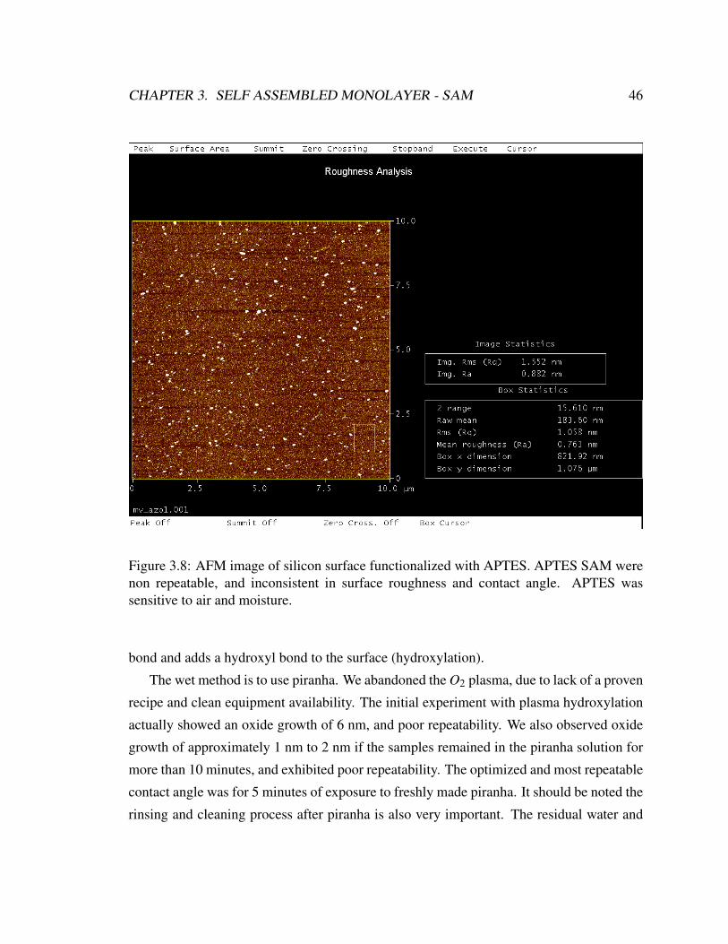
CHAPTER 3. SELF ASSEMBLED MONOLAYER - SAM 46
Figure 3.8: AFM image of silicon surface functionalized with APTES. APTES SAM werenon repeatable, and inconsistent in surface roughness and contact angle. APTES wassensitive to air and moisture.
bond and adds a hydroxyl bond to the surface (hydroxylation).
The wet method is to use piranha. We abandoned the O2 plasma, due to lack of a proven
recipe and clean equipment availability. The initial experiment with plasma hydroxylation
actually showed an oxide growth of 6 nm, and poor repeatability. We also observed oxide
growth of approximately 1 nm to 2 nm if the samples remained in the piranha solution for
more than 10 minutes, and exhibited poor repeatability. The optimized and most repeatable
contact angle was for 5 minutes of exposure to freshly made piranha. It should be noted the
rinsing and cleaning process after piranha is also very important. The residual water and

CHAPTER 3. SELF ASSEMBLED MONOLAYER - SAM 47
SiO
O
O
NH2
OH H
SiO O
H
O
NH2
SiO O
O
NH2
H2O
-EtOHSi
OO
NH2
- EtOHSi
O
O
O
NH2
Figure 3.9: APTES hydrolysis and condensation.
sulfuric acid catalyzes the reaction of silane with surface.
Figure 3.12 shows the Xray Photoelectron Spectrum (XPS) of a piranha cleaned
reference sample, the carbon on the surface is due to the long storage time of the sample in
air. However other elements besides silicon and oxygen are not present, we were especially
looking for sulfur residue due to sulfuric acid.
Sonication also plays an important role to remove the physically adsorbed monomers
and leave those covalently attached to the surface. Figure 3.13 shows the difference in
contact angle due to physically adsorbed monomers for Octyltrimethoxysilane. The sample
was sonicated for 60 second in toluene. A 36 change in contact angle was observed, we
hypothesized the contact angle change was due to physically adsorbed monomers. [72] The
contact angle change after sonication was not as dramatic when sufficient time was allowed
for complete formation of surface monolayer. Due to inconsistencies of determination
of optimum soak time to form a complete monolayer we discovered the significance of
sonication.

CHAPTER 3. SELF ASSEMBLED MONOLAYER - SAM 48
Figure 3.10: Summary of different adsorption mechanisms of APTES on SiO2 surface fromKristensen et al. a) Expected formation, free amine and covalently bonded to the surface.b) Protonated amine group and inversely bonded to the surface. c) Strong interaction dueto hydrogen bond of the amine and the surface silanol. d) Intermolecular hydrogen bondof the amine and silanol. e) Interaction of the amine and silicon. Reprinted from [70] withpermission from Elsevier.
NN
ON
Si
OO
HN
O
H2SO4/H2O2
Silicon <100>
Native Oxide
OH OHOH OH OH
Si
O
O
R
Si
O
O
R
Si
O
O
R
Si
O
O
R
Si
O
O
R
Si
O
OH
R
Native Oxide
OHOH OHOHOH
Si
O
O
R
Si
O
O
R
Si
O
O
R
Si
O
O
R
Si
O
O
R
Si
O
OH
R
Figure 3.11: SAM process overview
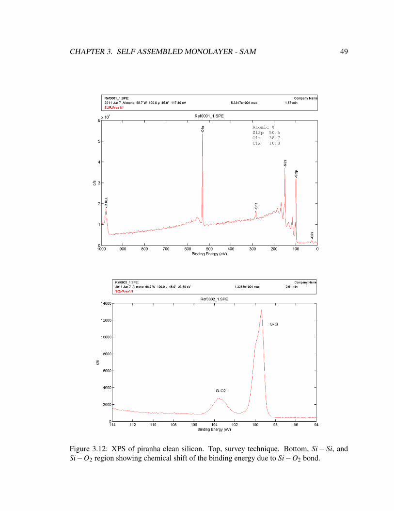
CHAPTER 3. SELF ASSEMBLED MONOLAYER - SAM 49
Figure 3.12: XPS of piranha clean silicon. Top, survey technique. Bottom, Si− Si, andSi−O2 region showing chemical shift of the binding energy due to Si−O2 bond.
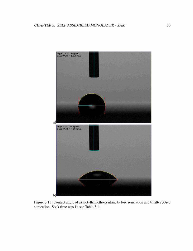
CHAPTER 3. SELF ASSEMBLED MONOLAYER - SAM 50
a)
b)
Figure 3.13: Contact angle of a) Octyltrimethoxysilane before sonication and b) after 30secsonication. Soak time was 1h see Table 3.1.
Chapter 4
Transduction
4.1 Piezoresistive cantilevers
Microelectromechanical systems based on piezoresistive sensing (resistance change with
stress) are especially interesting for displacement sensing and excel at dynamic measure-
ments. They are portable, low power, and disposable. Chemical and biosensing applica-
tions based on displacement transduction require static and low frequency measurement
stability over time periods of tens of seconds to many hours. Hence, the 1/f noise of the
piezoresistors becomes one of the limiting factors for their use as chemical sensors. The
work presented in this section is some of the basis for [73].
Typically, 1/f noise levels for piezoresistive, silicon microcantilevers are reported as
100-500 nV/ Hz at 1 Hz with corner frequencies ranging from 45 Hz to 10 kHz [74–77].
Many existing designs are intended for operation at frequencies where 1/f noise does not
limit resolution. We tailored fabrication process parameters to achieve the lowest 1/f noise
amplitude spectral density of which we are aware for piezoresistive cantilevers. These
results are part of an effort to study the noise and sensitivity of piezoresistive cantilevers
as a function of various processing parameters, including type of anneal (steam vs. inert),
anneal temperature and time, type of passivation oxide, chemical vapor-deposited, low
temperature oxide or thermally grown oxide, and implant dose and energy [78]. We found
that highly boron doped piezoresistors in the range of 1020 cm−3 exhibited the lowest 1/f
noise and the best signal to noise ratio.
51

CHAPTER 4. TRANSDUCTION 52
The cantilevers were fabricated from silicon-on-insulator, single-crystal silicon wafers,
and released by deep reactive ion etching. Piezoresistors were ion implanted with 50 keV
boron. Additional fabrication details are reported elsewhere [76, 79]. The piezoresistors
were placed close to the integral edge restraint, but 130 µm from the fixed end to avoid
the otherwise subtractive, transverse, tensile stress region near the fixed boundary. We used
four piezoresistors in a full-bridge for thermal stability. The full active bridge provides four
times the sensitivity and twice the noise of the typical single piezoresistor, increasing the
signal-to-noise ratio by 6 dB.
Figure 4.1A shows the placement of the resistors. The stress simulation and the
measured resonance frequency are shown in Figures 4.1B, and 4.1C, respectively. The
electrical schematic of the resistors appears in Figure 4.2. Notice that for a given stress,
the resistance of a resistor (p-type) that is parallel to the stress (longitudinal) increases
and the resistance of a resistor that is perpendicular (transverse) to the stress decreases.
This important layout scheme allows for first order common mode rejection of unwanted
effect such as temperature, package stress, and surface induced noise [80]. This layout
takes advantage of the fact that longitudinal piezoresistive coefficient of a p-type resistor
in < 110 > direction made in n-type < 100 > substrate is positive σl ∼ +π44/2, and the
transverse piezoresistive coefficient is negative σl ∼−π44/2. E110 =168 GPa, and π44 for
p-type piezoresistor in < 110 > is 138 x 10−11Pa−1 [81, 82].

CHAPTER 4. TRANSDUCTION 53
Figure 4.1: Placement of piezoresistor on the cantilever. A) Piezoresistor on the cantilever.B) Simulation of stress at the base of cantilever. C) Measured resonance frequency.Reprinted with permission from [73]. Copyright 2008, AIP Publishing LLC
Figure 4.2: Electrical schematic of the piezoresistor cantilever.

CHAPTER 4. TRANSDUCTION 54
Full 1/4-active Tortonese Pruitt Chui Harley Yu YuDose (cm−2), boron 5×10¹⁶ 1×10¹⁴ 5×10¹⁴ 1×10¹⁵ 5×10¹⁴ na 5×10¹⁴ 5 × 10¹⁵
Peak concentration (cm−3) 2.7×10¹⁹ 6.2×10¹⁷ 9×10¹⁸ 6×10¹⁸ 5×10¹⁴ 4×10¹⁸ na naAnneal temp (C) 1100 1000 1000 1000 1000 700 1050 950Anneal time (min) 50 52 10 40 10 180 30 10Spring constant (N/m) 1.5 17 5-100 1-85 1.6 0.01 na naSensitivity (V/N) 610 179 ˜2000 15 na 2×10⁶ na naωn (kHz) 1.6 3.7 40-800 1-6 280 50 12 naResistance (kΩ) 1.8 16.8 2.5-7 5.8 5-30 ˜16 na 3Johnson noise (nV/
√Hz) 5 16 9 10 9-22 16 14 6
Corner freq. (Hz) 0.6 20 45-750 200 200 1500 800 10, 0001/f noise at:10 Hz nV/
√Hz 5* 22 18 35 130 160 150-700 170
10 Hz (nV/V)/√
Hz 0.4* 6 5 5 26 32 25-117 281 Hz (nV/V)/
√Hz 1.2* 20 15 11 na na na na
0.1 Hz (nV/V)/√
Hz 3.7 na na na na na na na
Table 4.1: Selected process variables and performance characteristics for variouscantilevers including a full and a quarter active bridge with different doping and annealconditions, as well as several devices from the literature. In comparing 1/f noise, wenormalized the data by dividing by Vbias to achieve units of nV/(V ×
√Hz) or Hz−0.5.
nV/V is unitless, as is nΩ/Ω, which is appropriate since 1/f noise is a measure ofconductivity variation. Due to the low 1/f noise in this work, the total noise at the indicatedfrequencies is dominated by thermal noise and is denoted by *.
Table 4.1 compares noise of the full-bridge and single-resistor cantilevers, and
cantilevers from Tortonese [83], Pruitt [76], Chui [74], Harley [75] , Yu [77] , Yu [84],
and tabulates selected process and performance parameters where available. Highly doped
p-type resistors in the range of 1020 cm−3 concentration exhibit the lowest 1/f noise and
the best signal to noise ratio.
While aspects of 1/f noise remain controversial despite eight decades of research, [85]
the cause of 1/f noise is generally accepted to be conductivity fluctuations. Current flow
is needed only to convert resistance change to voltage change. For zero bias, only thermal
noise is present. To model 1/f noise, we use Hooge’s equation [86]:
SV =αV 2
biasN∆ f (4.1)
where N is the number of carriers, Vbias is the bias voltage, and α is an empirical

CHAPTER 4. TRANSDUCTION 55
Figure 4.3: Hooge coefficient (α) vs. diffusion length for this work and from the literature.Here we add our data for higher
√Dt, heavily doped piezoresistors to Harley’s plot [75] and
extend the trend line to show a lower minimum α value of 10−7 for single crystal silicon.
coefficient. N depends on piezoresistor volume and implant dose. α depends on crystal
lattice perfection [87]. Longer time and higher temperature anneals lowers α [88].√
Dt
(diffusion length), where D is the dopant diffusion coefficient and t is the anneal time, is a
measure of anneal effectiveness.
In Figure 4.3 we extend Harley’s [75] plot of α vs.√
DT with data from the current
study. The p-type silicon piezoresistor α value is significantly lower than metals α value
[89]. Gold, bismuth, copper, and aluminum, which have α values of approximately 10−3,
achieve low noise by high N. Here we report only selected devices with a 1/f exponent of
approximately 1, which as Fleetwood, [90] hypothesized, represents a minimum achievable
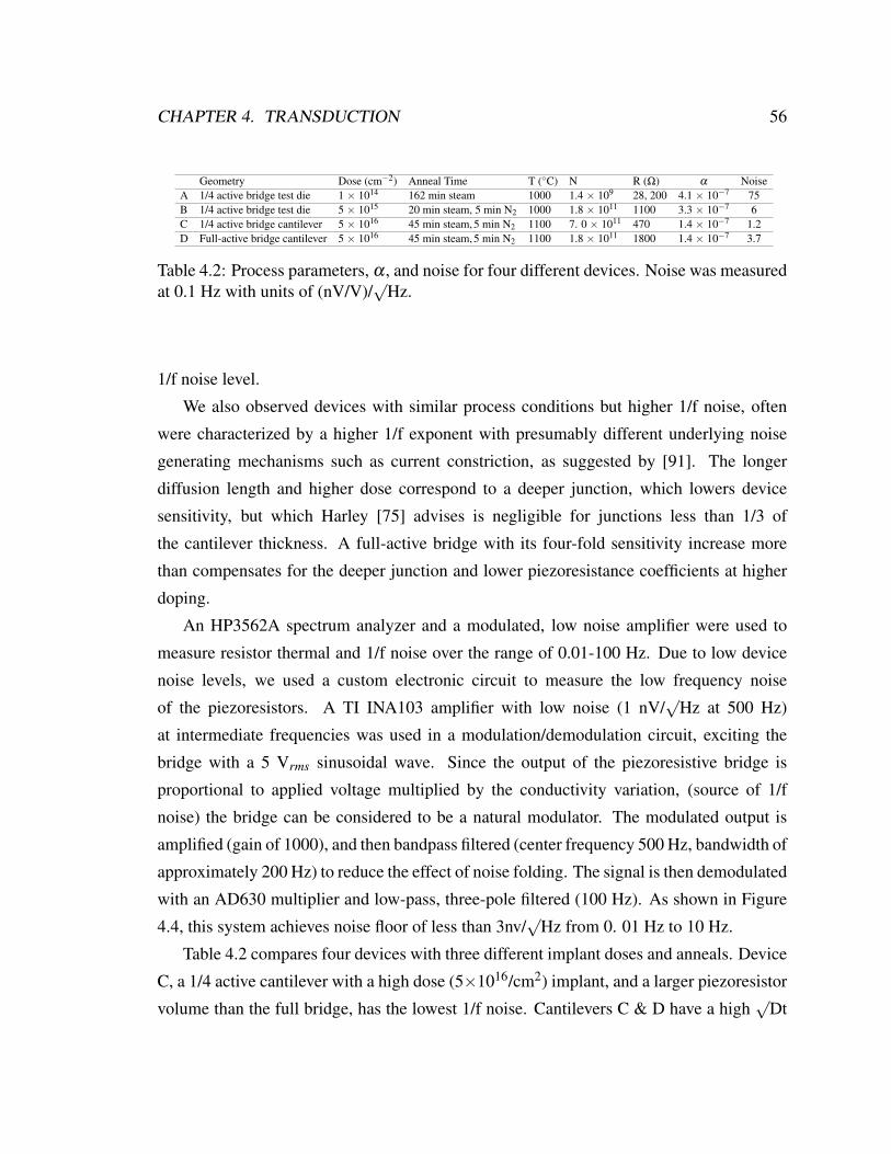
CHAPTER 4. TRANSDUCTION 56
Geometry Dose (cm−2) Anneal Time T (C) N R (Ω) α NoiseA 1/4 active bridge test die 1 × 10¹⁴ 162 min steam 1000 1.4 × 10⁹ 28, 200 4.1 × 10⁻⁷ 75B 1/4 active bridge test die 5 × 10¹⁵ 20 min steam, 5 min N2 1000 1.8 × 10¹¹ 1100 3.3 × 10⁻⁷ 6C 1/4 active bridge cantilever 5 × 10¹⁶ 45 min steam,5 min N2 1100 7. 0 × 1011 470 1.4 × 10⁻⁷ 1.2D Full-active bridge cantilever 5 × 10¹⁶ 45 min steam,5 min N2 1100 1.8 × 10¹¹ 1800 1.4 × 10⁻⁷ 3.7
Table 4.2: Process parameters, α , and noise for four different devices. Noise was measuredat 0.1 Hz with units of (nV/V)/
√Hz.
1/f noise level.
We also observed devices with similar process conditions but higher 1/f noise, often
were characterized by a higher 1/f exponent with presumably different underlying noise
generating mechanisms such as current constriction, as suggested by [91]. The longer
diffusion length and higher dose correspond to a deeper junction, which lowers device
sensitivity, but which Harley [75] advises is negligible for junctions less than 1/3 of
the cantilever thickness. A full-active bridge with its four-fold sensitivity increase more
than compensates for the deeper junction and lower piezoresistance coefficients at higher
doping.
An HP3562A spectrum analyzer and a modulated, low noise amplifier were used to
measure resistor thermal and 1/f noise over the range of 0.01-100 Hz. Due to low device
noise levels, we used a custom electronic circuit to measure the low frequency noise
of the piezoresistors. A TI INA103 amplifier with low noise (1 nV/√
Hz at 500 Hz)
at intermediate frequencies was used in a modulation/demodulation circuit, exciting the
bridge with a 5 Vrms sinusoidal wave. Since the output of the piezoresistive bridge is
proportional to applied voltage multiplied by the conductivity variation, (source of 1/f
noise) the bridge can be considered to be a natural modulator. The modulated output is
amplified (gain of 1000), and then bandpass filtered (center frequency 500 Hz, bandwidth of
approximately 200 Hz) to reduce the effect of noise folding. The signal is then demodulated
with an AD630 multiplier and low-pass, three-pole filtered (100 Hz). As shown in Figure
4.4, this system achieves noise floor of less than 3nv/√
Hz from 0. 01 Hz to 10 Hz.
Table 4.2 compares four devices with three different implant doses and anneals. Device
C, a 1/4 active cantilever with a high dose (5×10¹⁶/cm2) implant, and a larger piezoresistor
volume than the full bridge, has the lowest 1/f noise. Cantilevers C & D have a high√
Dt

CHAPTER 4. TRANSDUCTION 57
Figure 4.4: System noise floor and amplitude noise spectra for four piezoresistors. Thehigher doped devices with longer and higher temperature anneals display less noise. Thesystem noise floor down to 0.01 Hz was verified to be lower than 3 nV/
√Hz by measuring
the Johnson-dominated noise of a 680 ohm metal wire wound resistor bridge with 18 mVrmsexcitation.
anneal and consequently a low α . For the full-active bridge at a full-scale output of 200
mV at 5 Vbias, in the band 0.01-10 Hz, the dynamic range was >140 dB.
We determined cantilever sensitivity using a previously reported Laser Doppler Vi-
brometer technique [76,79] our result was confirmed by thermomechanical excitation (Fig.
4.1C). The force sensitivity of the full-active bridge was 10 pN/√
Hz at 1 Hz with amplitude
resolution of 6 pm/√
Hz. The force resolution was 100 pN for the frequency band of 0.1-
100 Hz. These low noise results are promising for the design of piezoresistive devices for
low frequency measurements, a key prerequisite for the chemical sensing applications.
CHAPTER 4. TRANSDUCTION 58
4.2 Design
The optimization of the design of tip loaded piezoresistive cantilevers is different from
design of piezoresistive cantilevers optimized for surface stress. [92]. Here we derive the
tip deflection for a distributed surface stress loaded cantilever and highlight the fundamental
differences between tip loaded and distributed loaded cantilevers. The optimization of tip
loaded cantilever was reported by Park, Rastegar et al. [93].
d2ydx2∼=
1R=
ME∗I
y(0) = 0dydx
(0) = 0 (4.2)
E∗ =E
1−ν(4.3)
M = σwt/2 I = wt3/12 (4.4)
y =Mx2
2E∗I(4.5)
κ =1R=
6σ
E∗t2 (4.6)
R∼ l2
2∆y(4.7)
∆y = 3σ
E∗(lt)2 (4.8)
Equation 4.8 is the tip deflection of a cantilever based on surface stress. Note the
unit of surface stress is N/m, and that of surface energy J/m2 [94]. The key assumptions
here are thin film and small curvature. The thin film assumes that the position of neutral
axis remains the same. In a beam, the neutral axis does not change its length when the
beam is bent (dashed lines in Fig. 4.5A, B). The approximation of Equation 4.7 assumes
small curvature. In Figure 4.5, the cantilever is under uniformly loaded surface stress
σ . This surface stress effect is modeled as a concentrated moment M applied at the
cantilever beam’s free end. I is the moment of inertia given by Equation 4.4 for a beam
with rectangular cross section. l, w, and t are the length, width, and thickness of the beam,
respectively. E is the Young’s modulus and E∗ is the biaxial modulus. When the beam
is horizontally stretched its thickness reduces, which is given by Poisson’s ratio ν . The

CHAPTER 4. TRANSDUCTION 59
X
Y
σ
A
B C
l
w
Figure 4.5: A) Cantilever model and coordinate system. B) Compressive surface stress. C)Tensile surface stress. A mnemonic tip to remember the convention is to look at the bottomsurface of the film, and remembering tensile stress has a positive sign.
governing differential equation for an elastic beam is given by Equation 4.2, where R is the
radius of curvature.
Note that Equation 4.4 gives the moment in terms of surface stress, width, and thick-
ness; however, the radius of curvature is only proportional to surface stress and the square
of the thickness (Equation 4.6). Equations 4.4 and 4.6 reveal the fundamental difference
between distributed loaded cantilevers and tip loaded cantilevers. In a piezoresistive tip
loaded cantilever, the moment at the base is simply the force at the tip multiplied by the
length of cantilever. The piezoresistors are placed at the base of the cantilever near the
top surface, since maximum stress occurs at the surfaces near the base. However, for
a distributed loaded cantilever that is not the case. Table 4.3 summarizes the important
differences between surface stress cantilevers and tip loaded cantilevers. For surface stress

CHAPTER 4. TRANSDUCTION 60
Surface stress Tip loadedTip deflection ∆y = 3σ f
E∗ ∗ (l/t)2 ∆y = 4FE∗w ∗ (l/t)3
Change in resistance ∆ρ
ρ= πlσl +πtσt
∆ρ
ρ= πlσl +πtσt
Output voltage Vout ≈ 3σ fts∗ π44
2 ∗Vin Vout ≈ 6Flwt2
s∗ π44
2 ∗Vin
Table 4.3: Distributed load cantilever versus tip loaded cantilever. Full bridge configurationof the piezoresistor is assumed. Vin is the bridge voltage.
based cantilevers it is important to note that reducing the thickness and increasing the length
of the cantilever will maximize tip deflection. However, for piezoresistive surface stress
cantilevers only reducing the thickness maximizes the output voltage [95].
4.3 Electrical noise
Noise is any unwanted signal. Electrical noise is the random variation of potential between
the ends of a conductor. The electrical noise in a piezoresistor sets the fundamental lower
limit of piezoresistive transducer resolution. In this section, we focus our discussion on the
dominant random electrical noise sources in piezoresistors: Johnson or thermal noise and
1/f or flicker noise. Note that current noise or shot noise due to the direct current through a
resistor at low current values (approximately 1 mA) is not significant. Other noise sources
such as inductive or capacitive line pickup also exist, but they are not random in nature and
are not discussed [96]. For many applications, the accuracy of piezoresistive transducers
is limited by temperature effects or thermo-mechanical hysteresis, e.g., in commercial
piezoresistive devices such as piezoresistive pressure sensors. Integrated shield layers have
been shown to reduce noise effects, including temperature sensitivity [97].
4.3.1 Thermal noise
Thermal noise, also known as Johnson or Johnson-Nyquist noise, is universal to all
resistors. It was first observed by Johnson and theoretically explained by Nyquist [98] in
1928. Johnson attributed ”the statistical fluctuation of electric charge in the conductor”
as the source of noise and measured the effect of these fluctuations via vacuum-tube

CHAPTER 4. TRANSDUCTION 61
resistance.
VJ =√
4kbT R (4.9)
Thermal noise is related to the absolute temperature T (K) of the resistor, resistance
value R(Ω), and Boltzmann’s constant kb(J/K). The root mean squared value of voltage
across a resistor in 1 Hz bandwidth is shown by Equation 4.9. Thermal noise in any resistor
is fundamental, cannot be eliminated, and is independent of the material that the resistor is
made of. Since Equation 4.9 only depends on temperature and resistance, it can be used as
an absolute calibration method for systems if the temperature and the resistance are known.
4.4 Flicker noise
Flicker or 1/f noise, as its name implies, has a power spectrum that is inversely proportional
to frequency. The origins of 1/f noise are still not fully understood and remains an active
topic of research [86], [99]. In particular, 1/f noise in piezoresistors is dependent on
fabrication process parameters, such as implant parameters (dose and energy) and type
of anneal [100]. 1/fn noise is also a good measure of the quality of resistors [101]; noise
in excess of the normal value, or a non-unity slope n > 1 are indicative of poor fabrication
process quality [102]. Researchers have optimized piezoresistive device performance while
taking into consideration 1/f noise [75, 77]. Despite many decades of research, the source
of 1/f noise is still debated [103]. McWhorter and Hooge proposed two opposing theories
on the source of 1/f noise. These views are currently the leading explanations for the origin
of 1/f noise.
Figure 4.6 shows these models graphically. The McWhorter model attributes the 1/f
noise to surface defects, while the Hooge model implicates bulk defect [105]. Experimental
results show that 1/f noise is due to fluctuation in the conductivity of the carriers [88].
Hooges shows that 1/f low frequency noise modulated the thermal noise when no current
was passed through the resistor [85]. This experiment demonstrates that 1/f noise is not
current-generated. In a typical measurement, current is only needed to transform the
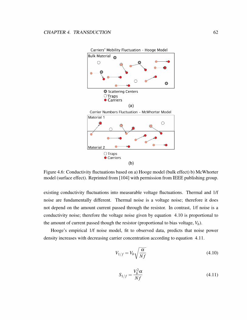
CHAPTER 4. TRANSDUCTION 62
Figure 4.6: Conductivity fluctuations based on a) Hooge model (bulk effect) b) McWhortermodel (surface effect). Reprinted from [104] with permission from IEEE publishing group.
existing conductivity fluctuations into measurable voltage fluctuations. Thermal and 1/f
noise are fundamentally different. Thermal noise is a voltage noise; therefore it does
not depend on the amount current passed through the resistor. In contrast, 1/f noise is a
conductivity noise; therefore the voltage noise given by equation 4.10 is proportional to
the amount of current passed though the resistor (proportional to bias voltage, Vb).
Hooge’s empirical 1/f noise model, fit to observed data, predicts that noise power
density increases with decreasing carrier concentration according to equation 4.11.
V1/ f =Vb
√α
N f(4.10)
S1/ f =V 2
b α
N f(4.11)

CHAPTER 4. TRANSDUCTION 63
where S1/ f ,V1/ f , f ,N,Vb, are the Hooge noise power density, Hooge noise, frequency,
total number of carriers in the resistor volume, and bias voltage across the resistor,
respectively. A non-dimensional fitting parameter, α , is ascribed to the ”quality of the
lattice” and typically ranges from 10−3 to 10−7.
Attempts to observe the lower limit of 1/f, below which the spectrum flattens, have not
been successful because of the more dominant Johnson noise [85]. Measurements down
to 3µ Hz showed that the noise spectrum is still 1/f [106]. Harley showed that resistors
with the same surface to volume ratio have different 1/f noise characteristics and 1/f noise
scales with the volume of the resistors, consistent to Hooge empirical equation [75]. Hooge
defines 1/f noise as only those spectra with a frequency exponent of 0.9-1.1 [99], [107].
Noise with different spectral density and other frequency exponents, sometimes referred to
as 1/f-like noise, is not predicted by the Hooge equation and is often confused with the 1/f
noise [85], [105].
According to Hooge, noise with higher exponent of 1.5 or 2, is an indication of noise
mechanisms other than lattice fluctuations and should not be treated as 1/f noise. These
mechanisms could give insights into reliability and failure analysis of piezoresistors. For
example, Neri found that the exponent in 1/f is closer to 2 in metal traces that exhibit
electromigration [107] .
Vandamme also showed excess 1/f noise in semiconductors can be attributed to small
constriction and current crowding [91]. The third harmonic appears when a low frequency
(less than 1 MHz) sine wave is applied to piezoresistors with current flow paths that
contained constrictions. Applied power heats small constrictions in the resistor and
changes the resistor value proportional to the temperature coefficient of the piezoresistor.
Therefore, the input excitation exhibits a cubic nonlinearity. Current crowding theory
also explains why polysilicon has higher 1/f noise than crystalline silicon [99]. At grain
boundaries, small constrictions are present, thus reducing the total number of carriers (N)
and effectively increasing the 1/f noise. Basically 1/f voltage noise does increase linearly
with the applied excitation. If the noise spectrum trends otherwise, then other mechanisms,
such as current crowding, could be present. The noise floor of the experimental setup may
be verified by reducing the applied excitation and observing only the thermal noise of the
piezoresistor.

CHAPTER 4. TRANSDUCTION 64
Figure 4.7: 1/f resistor noise measuring block diagram.
4.4.1 Circuit for measuring resistor flicker noise
We did not have access to commercially available instruments that directly measure resistor
noise such as Stanford research SRS830 lock-in amplifier and Keithley model 6220/2182A
current generator. Also, we did not find any amplifier that had less than 4 nV/√
Hz at
0.01 Hz. Hence, an alternative electronic circuit was devised in order to measure the low
frequency noise of our piezoresistive cantilevers.
An HP3562A spectrum analyzer in conjunction with a modulated low noise amplifier
was used to measure the resistor thermal and 1/f noise in the range of 0.01 Hz - 1000 Hz.
The initial circuit used a INA103 instrumentation amplifier, which has 1 nV/√
Hz, at a
spot frequency of 1 kHz. However, the instrumentation amplifier input referred voltage,
and input current noise at low frequency were 40 nV/√
Hz and 30 pA/√
Hz, respectively,
at a spot frequency of 1 Hz. This high flicker noise became a limiting factor.
However, by use of modulation we were able to reject the amplifier flicker noise. Note
that INA103 has high input bias current, bridge resistances of greater than 5 kΩ are not
recommended for use with the INA103 front end. Since the amplifier has lower noise at
higher frequencies, for example, 1 nV/√
Hz at 500 Hz, INA103 can provide the basis for a
low flicker noise design if the circuit is operated at 500 Hz.
The output of the bridge is proportional to the applied voltage times the conductivity
variation, the bridge is a natural modulator; the output voltage of the bridge is a

CHAPTER 4. TRANSDUCTION 65
multiplication of the change in resistivity ∆R and the bridge voltage Vb. Exciting the bridge
with an AC signal and then amplifying the modulated signal will prevents operation a the
region of high flicker noise. Demodulating the signal back to low frequency provides the
solution. This technique was commonly used in the early days of radios and is the basis for
lock-in amplifier design.
Figure 4.7 illustrates the block diagram of the circuit. The sensor conductivity
fluctuation is modulated at the desired frequency, and amplified by a gain of 1000 using
INA103. The signal then passes through a passive band pass filter with a bandwidth of
approximately 200 Hz and center frequency of 500 Hz to reduce noise folding into the
baseband after demodulation. The signal then is demodulated using the AD630 with a gain
of 4/π .
After demodulation, the signal passes through a third-order passive filter. An external
low phase noise oscillator is paramount, since the phase noise of the oscillator will directly
contribute to the flicker noise. The 500 Hz modulation frequency was chosen primarily
due to limitations of the AD630. The actual circuit implementation of the 1/f resistor noise
Figure 4.8: 1/f resistor noise measuring circuit implementation.

CHAPTER 4. TRANSDUCTION 66
block diagram appears in Figure 4.8.
4.5 Calibration
Several methods to calibrate cantilever sensitivity have been previously discussed [108].
However, the simplest and quickest method is the thermo-mechanical noise calibration. As
discussed on page 61, noise can also be used to calibrate a system.
Since the detector output of the AFM only provides a voltage, a constant is needed to
convert the voltage into the actual tip displacement. Ref. [109] refers to the calibration
constant as inverse optical lever sensitivity (InvOLS).
The tip deflection was calibrated by measuring the thermo-mechanical noise of the
cantilevers, using equations in this section to calibrate the cantilever tip deflection and
ultimately surface stress.
Equation 4.12 equates the thermal noise energy to the energy of the cantilever where
k is the spring constant of the cantilever and z is the tip deflection. This equation is valid
for cantilevers of any shape or material. Equation 4.13 is the total amount energy at room
temperature (27C). kb is the Boltzman constant and T is the temperature in units of Kelivn.
kbT can be thought of as 4.1 *10−21 J or 4.1 nm-pN (nanometer*pico Newton) or 0.026
electron volt (eV).
Equation 4.14 is the force constant of the cantilever from the mechanical dimensions; l
is length, w is width, and t is thickness, and E is Young’s modulus. k is dependent on the
shape and the material that the cantilever is made of. We used a rectangular cantilever.
In order to maximize the tip deflection of the cantilever for a surface stress caused by
chemical binding, from Equation 4.26 it is apparent that the cantilever should be as long
and as thin as possible to maximize the (l/t)2.

CHAPTER 4. TRANSDUCTION 67
1/2kbT = 1/2kz2 (4.12)
kbT = 4.1∗10−21Joules (4.13)
k =Ewt3
4l3 (4.14)
f0vac =
√k
Me(4.15)
Me = 0.2427∗M (4.16)
The vacuum resonance frequency f0vac of a rectangular cantilever is given by Equation
4.15, where Me is the normalized effective mass, which is equal to 0.2427 of beam mass
(M) for rectangular beams of l/w > 5 [110]. For our chemical sensing cantilevers l is 500
µm w = 100 µm and t = 1 µm. Our cantilevers were purchased from Nanoworld and were
made of pure silicon in the < 110 > direction. Silicon has Young’s modules of Exy=169
GPa in the < 110 > direction and a Poisson ratio of νxy= 0.06 [81].
There were significant differences in cantilever thickness from device to device. The
manufacturer specifies a thickness range of 0.5 µm - 2.5 µm with a typical thickness of
1 µm, which is understandable due to etching tolerances. Length varied ±1% and width
by ±5% which are within the lithographic tolerances of ± 5 µm. Since measurement of
thickness is rather difficult and destructive, each cantilever must be calibrated using the
thermo-mechanical noise before use.
Our strategy for cantilever calibration was:
• Fit the noise from the cantilever’s fundamental resonance mode to a simple harmonic
oscillator;
• From the value of resonance frequency, solve for cantilever thickness;
• From the thickness, find the spring constant k;
• Integrate the resonance voltage noise over the bandwidth and equate it to the energy
to solve for tip displacement and InvOLS;
• From tip displacement and Stoney’s equation, solve for surface stress.

CHAPTER 4. TRANSDUCTION 68
The power response of a simple harmonic oscillator is given by Equation 4.17, where
α is the normalization factor, and Q is the ratio of energy stored to energy lost, which is
given by Equation 4.18 where ∆ f is the 3 dB bandwidth. A key simplification equates the
vacuum resonance frequency to the measured resonance frequency. Equation 4.19 relates
the vacuum resonance frequency to the damped resonance frequency. If Q > 10, then the
error is less than 1%.
G( f ) =α
(1− ( f 2
f 20)2 + ( f/ f0)2
Q2
(4.17)
Q =f0
∆ f(4.18)
fd = f0
√1− 1
2Q(4.19)
t = 2π f0l2
√.968ρ
E(4.20)
Equations 4.15 and 4.14 are solved to yield the thickness in Equation 4.20, where l is
the length of rectangular cantilever (500 µm) E = E110 (169 GPa), and ρ is the density of
silicon (2330 kg/m3).
Figure 4.9 shows the voltage noise spectral density from AFM. The Q of the cantilever
acts as a mechanical gain source that amplifies the random collision of air molecules
(thermo-mechanical noise) with the cantilever surface. Therefore, the peak voltage is the
thermo-mechanical noise amplified by Q.
The total noise power is given by Equation 4.21, where G( f ) is the transfer function of a
simple harmonic oscillator and P( f ) is the thermo-mechanical noise power spectrum. The
equation simplifies to noise bandwidth times the amplified noise power (Eq. 4.23) [111].
Note that f0/Q is bandwidth ∆ f , and π
2 ∆ f is the equivalent noise bandwidth. Pdc can be
determined from the resonance noise voltage of Figure 4.9 divided by Q. The cantilever tip
movement due to thermo-mechanical noise is given by Equation 4.24, hence the sensitivity
(InvOLS) is given by Equation 4.25 which is the ratio of equation 4.24 and 4.21.

CHAPTER 4. TRANSDUCTION 69
Figure 4.9: Cantilever tip deflection voltage noise spectral density (orange circles), and fitto a simple harmonic oscillator noise transfer function (black line) taking into account 1/fand white noise .

CHAPTER 4. TRANSDUCTION 70
∆V 2 =∫
G( f )2P( f )d f =π
2f0QPdc (4.21)
Pdc = (Resonance−noise− voltage
Q)2 (4.22)
∆V 2 = (Resonance−noise− voltage)2 ∗ π
2∆ f (4.23)
∆y2 =KbT
k(4.24)
InvOLS = Sensitivity =
√KbT
k2
πQ f0Pdc(m/V ) (4.25)
The last task is to relate cantilever tip deflection to surface stress. Equation 4.26 can be
solved for surface stress (Eq. 4.27). Surface stress per volt is given by Equation 4.28.
∆y = 3σ
E∗(lt)2 (4.26)
σ = (tl)2 E∗∆y
3(N/m) (4.27)
Ss = (tl)2 E∗
3
√KbT
k2
πQ f0Pdc(N/m/V ) (4.28)
Chapter 5
Measurements
In this section we discuss functionalization, mounting, measurements, and experiments
which validated tip deflection of cantilever was due to MR-APTES mono layer.
Optomechanical modulation of the cantilever was measured by the optical beam bounce
method using Witec-Alpha AFM. Figure 5.1 shows the setup. Extreme care was taken to
isolate the cantilever from any mechanical coupling. A 405 nm solid-state laser was placed
beneath the cantilever, and the illumination intensity was set by a custom-made laser driver.
The on-off time of the laser was set by a waveform generator. The cantilever was placed
on a glass slide (Corning 2947) in air. When the MR-APTES was exposed to the 405 nm
laser, the molecule isomerized from trans to cis; when the laser was turned off, the molecule
reverted back to the more energetically favorable trans configuration. The cis configuration
occupied more space than the trans configuration, and hence, the cantilever accommodated
this change in volume by bending. Reprinted with permission from [44]. Copyright 2013
American Chemical Society.
71

CHAPTER 5. MEASUREMENTS 72
Position
Sensor
Position
LASER
Coated
Cantilever
Collimating Lens
405nm
LASER
Actuator
Figure 5.1: Representation of measurement setup (not drawn to scale).
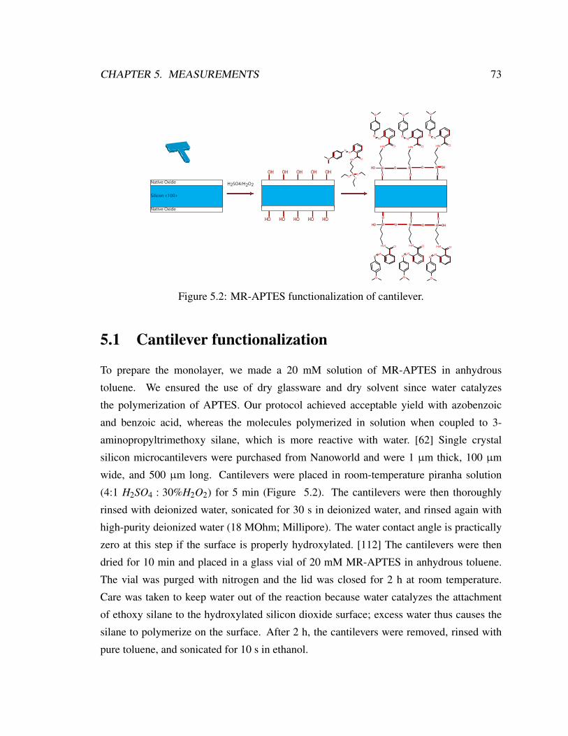
CHAPTER 5. MEASUREMENTS 73
NN
ON
Si
OO
HN
O
H2SO4/H2O2
Silicon <100>
Native Oxide
OH OHOH OH OH
Native Oxide
OHOH OHOHOH
Si
O
O Si
O
Si
O
OH
NN
O
N
HN
NN
O
N
HN
NN
O
N
HN
OOH
Si
O
O Si
O
Si
O
OH
NN
O
N
HN
NN
O
N
HN
NN
O
N
HN
OOH
Figure 5.2: MR-APTES functionalization of cantilever.
5.1 Cantilever functionalization
To prepare the monolayer, we made a 20 mM solution of MR-APTES in anhydrous
toluene. We ensured the use of dry glassware and dry solvent since water catalyzes
the polymerization of APTES. Our protocol achieved acceptable yield with azobenzoic
and benzoic acid, whereas the molecules polymerized in solution when coupled to 3-
aminopropyltrimethoxy silane, which is more reactive with water. [62] Single crystal
silicon microcantilevers were purchased from Nanoworld and were 1 µm thick, 100 µm
wide, and 500 µm long. Cantilevers were placed in room-temperature piranha solution
(4:1 H2SO4 : 30%H2O2) for 5 min (Figure 5.2). The cantilevers were then thoroughly
rinsed with deionized water, sonicated for 30 s in deionized water, and rinsed again with
high-purity deionized water (18 MOhm; Millipore). The water contact angle is practically
zero at this step if the surface is properly hydroxylated. [112] The cantilevers were then
dried for 10 min and placed in a glass vial of 20 mM MR-APTES in anhydrous toluene.
The vial was purged with nitrogen and the lid was closed for 2 h at room temperature.
Care was taken to keep water out of the reaction because water catalyzes the attachment
of ethoxy silane to the hydroxylated silicon dioxide surface; excess water thus causes the
silane to polymerize on the surface. After 2 h, the cantilevers were removed, rinsed with
pure toluene, and sonicated for 10 s in ethanol.

CHAPTER 5. MEASUREMENTS 74
Figure 5.3: A cantilever attached to a magnetic washer. The thermal mismatch ofexpansions was a major source of error. For all data presented, the cantilevers were placedon a low absorbance glass slide (Corning 2947).
5.2 Mounting of the cantilevers
Initially, the cantilevers were mounted in the system based on the recommendations of the
manufacturer of the AFM. The cantilever was fastened to a magnetic washer using epoxy
(Fig. 5.3). However, we measured consistently excessive high signal levels. We detected
motion even on the reference cantilever, which fortunately had different characteristics than
the functionalized cantilever. We hypothesized existence of the photon momentum transfer
however, the photon forces are in the order of pN for a 10 mW laser light, which could
not explain the observed massive deflections [113]. After a great deal of investigation,
we identified a mismatch between the thermal expansion coefficient of the metal washer,
the epoxy, and the silicon that caused the observed excessive cantilever tip deflection.
Hence the cantilevers were placed on low absorbance glass slides (Corning 2947) to prevent
thermal mismatches and convection heating of the air surrounding the cantilever.
Substantial noise and drift were detected in the reference bare cantilever and the MR-
APTES coated cantilever raw deflection as shown in Figure 5.4. The cantilever beams

CHAPTER 5. MEASUREMENTS 75
Figure 5.4: The signal from a bare silicon cantilever. The horizontal axis is time in secondsand the vertical axis is the output voltage of the top-bottom detector of the AFM. Thisvoltage is proportional to the tip deflection of the cantilever. For each cantilever, theproportionality constant was calibrated based on the equations developed in section 4.5.The sensitivity for this cantilever was 46 nm/V.
were soft in order to maximize the effect of surface stress, which made them more
susceptible to environmental noise. The spring constant of cantilevers were approximately
30 mN/m. Figure 5.5 shows the signal from the MR-APTES coated cantilever. The power
of modulation becomes intuitively apparent, as we can detect the periodic signal in the
noisy waveform of Figure 5.5. Since the frequency of excitation is precisely known, with
processing we can filter around the known excitation frequency and reject broadband noise.
The repetitive nature of the input signal also allowed for averaging and improved signal to
noise ratio by orders of magnitude. Random white noise is not repetitive, and it has zero
average. Hence, by simply cycle averaging the signal and noise the repeatable portion of
the signal appears.

CHAPTER 5. MEASUREMENTS 76
0 20 40 60 80 100 120−0.35
−0.3
−0.25
−0.2
−0.15
−0.1
−0.05
0MR Canti2−Right.mat
50 50.5 51 51.5 52 52.5 53 53.5
−0.24
−0.22
−0.2
−0.18
−0.16
−0.14
−0.12
−0.1
−0.08
MR Canti2−Right.mat
Figure 5.5: The signal from the MR-APTES coated cantilever. Top, the entire signal (120s). Bottom expanded view of several cycles.

CHAPTER 5. MEASUREMENTS 77
Figure 5.6: MR-APTES cantilever tip deflection spectrum.
5.3 Signal processing
Initially, we used a HP3564 spectrum analyzer for data acquisition. However, using Matlab
and a National instrument data acquisition card was more versatile. We used the spectrum
analyzer to validate our measurement setup and found better than 0.1% agreement between
the instruments. The absolute voltage measurement accuracies were important, since they
directly relate to tip deflection measurement errors. We used a 100 Hz anti-aliasing filter
to collect data. The raw AFM voltage spectrum of tip deflection of the MR-APTES coated
signal is shown in Figure 5.6.
A finite impulse response filter with 16384 tap was designed to filter the main harmonic.
The filter had a center frequency of 1 Hz and bandwidth of 0.1 Hz. The frequency response

CHAPTER 5. MEASUREMENTS 78
Figure 5.7: Finite impluse response of band pass filter used to filter the data.
and phase of the filter are shown in Figure 5.7.
The input signal and the output signal of the filter appear in Figure 5.8. Note the absence
of the drift and the delay in the output signal. Since the filter is bandpass, the low frequency
components are taken out. The delay is due to the inherent nature of limited bandwidth.
The time constant for 0.1 Hz bandwidth is 10 s. There were 16384 taps with the sample
frequency of 1 kHz which will result in 16.384 seconds delay for the filter, with a linear
phase. The output signal in time domain mainly resembles a sine wave. Such filtering lends
well for design of lock-in instrumentation amplifiers, which identifies whether a signal is
present among large noise. However important aspect of the signal, such as rise and fall
times, are lost. Upon verification of the signal, we used spectral analysis and averaging to
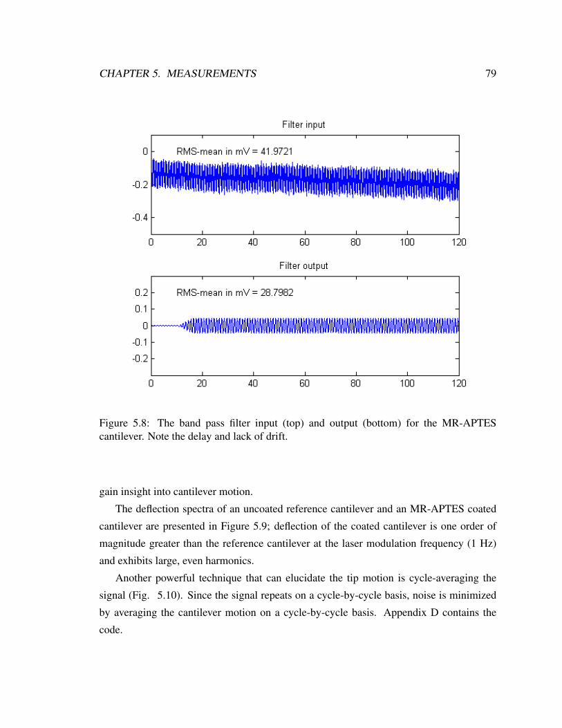
CHAPTER 5. MEASUREMENTS 79
Figure 5.8: The band pass filter input (top) and output (bottom) for the MR-APTEScantilever. Note the delay and lack of drift.
gain insight into cantilever motion.
The deflection spectra of an uncoated reference cantilever and an MR-APTES coated
cantilever are presented in Figure 5.9; deflection of the coated cantilever is one order of
magnitude greater than the reference cantilever at the laser modulation frequency (1 Hz)
and exhibits large, even harmonics.
Another powerful technique that can elucidate the tip motion is cycle-averaging the
signal (Fig. 5.10). Since the signal repeats on a cycle-by-cycle basis, noise is minimized
by averaging the cantilever motion on a cycle-by-cycle basis. Appendix D contains the
code.

CHAPTER 5. MEASUREMENTS 80
Figure 5.9: MR-APTES enables optomechanical actuation of microcantilevers. When abare silicon reference cantilever (left) is excited with a 405-nm laser at 1 Hz, a small peakappears at the modulation frequency and even harmonics are not visible. The deflectionamplitude of a cantilever functionalized with MR-APTES (right) increases 10-fold at themodulation frequency and even harmonics are visible in the spectrum due to the differencein the on- and off-rates of actuation.
Figure 5.10: Optomechanical motion of the cantilever. Left, raw output of the AFM tipdeflection for an MR-APTES-coated cantilever. Right, mean corrected cycle average of119 pulses of the MR-APTES (orange) and the reference cantilever (blue). The uncoatedreference cantilever does not show motion, while the MR-APTES coated cantilever does.One hundred nineteen pulses were averaged to improve the signal to noise ratio. The turn-on time is substantially faster than the turn-off time due to the finite rate of cis-trans thermalisomerization.

CHAPTER 5. MEASUREMENTS 81
5.4 Analysis of tip motion due to heat
Heating and cooling can also cause tip deflection. By measuring tip deflection at different
wavelengths that can cause the same amount of heat, we can rule out the effect of heat.
We used a laser with a wavelength at which MR-APTES does not isomerize (635 nm;
Fig. 5.11). At both wavelengths, most of the heat generated was due to the absorption
of photons by the silicon cantilever rather than by the monolayer. Yi et al. [114] reported
an absorbance of 8 ∗ 10−3 for two MR-APTES monolayer (both side of glass slide) at a
maximum absorbance wavelength of 435 nm. Therefore, most of the light is transmitted
through the MR-APTES into the silicon. The absorption coefficient of silicon is 1.0 x
107/m and 3.5 x 10⁵/m at 405 nm and 635 nm, respectively; therefore, the incident light is
efficiently absorbed by the 1000 nm thick cantilever beam in both cases. When we varied
the laser power at 405 nm from 1 mW to 8 mW, we observed a linear increase in the
amplitude of deflection and did not observe any discernible response at 635 nm when the
power was varied.
By observing tip deflection in the frequency domain, it is possible to gain more
insight about the signal. For example, in the cycle average of the reference cantilever,
Figure 5.11: An MR-APTES-coated cantilever exhibits actuation when excited with 405nm laser, and no actuation when excited with a 635 nm laser. The laser power wasapproximately 2 mW for both wavelengths. The wavelength specificity is consistent withan optomechanical rather than thermal actuation mechanism.

CHAPTER 5. MEASUREMENTS 82
Figure 5.12: Cantilevers coated with a non-photoswitchable (11-bromoundecyltrimethoxysilane) SAM do not exhibit actuation. The laser powerused here was the same as that used with MR-APTES-coated cantilevers (2 mW).
the tip deflection at 1 Hz was obscured by noise, but we detect a small peak in the
frequency domain with the functionalized cantilever. A perfectly symmetrical square
wave in which the on and off times are identical shows only odd harmonics, which
can be mathematically shown by Fourier analysis. For the gold-coated and reference
cantilevers, we only observe odd harmonics that are related to the equal on and off times.
As expected, the heating (light on) and cooling (light off) mechanisms are symmetric. In
the case of MR-APTES, the photostationary states are reached faster during illumination
than when the molecule is allowed to reach a stationary state in the dark. Therefore,
the on and off times are asymmetric even though the input is symmetric, an effect that
appears as even harmonics in the Fourier spectrum. In summary, the presence of even
harmonics suggests asymmetry between the on and off times of the cantilever: thermal
actuation is symmetric, while optomechanical actuation is not. This difference is due
to the MR-APTES SAM. To investigate the effects of cantilever heating, we used gold
and 11-Bromouncyltrimethoxysilane coated (Fig. 5.12) cantilevers. Figure 5.13 shows tip
deflection of a gold-coated cantilever excited with less than 100 µW laser power. The 1 µm
thick silicon layer of the gold-coated cantilever absorbs the transmitted light and converts it
to heat. The thermal coefficient of expansion of silicon is 2.6 ppm/K and the coefficient for
gold is 14 ppm/K. Because the metal is only deposited on the top of the cantilever, the heat

CHAPTER 5. MEASUREMENTS 83
Figure 5.13: Time (left) and frequency domain (right) of the tip deflection of a gold-coatedcantilever. The silicon-gold bimorph structure deflects due to the temperature increaseinduced by the incident optical power (< 100 µW). Even harmonics are not present in thesignal because the heating and cooling rates are the same. One hundred nineteen pulseswere averaged.
expands the metal and the cantilever bends downward to accommodate this expansion.

Chapter 6
Discussion and conclusion
We have shown by modulation techniques that small surface stresses can repeatedly and
reliably be measured. Due to the success of our approach, a fundamental follow up question
that arose was “how do surface stresses of various component interact ”. In this Chapter
we present an approach and preliminary data for the aforementioned question.
According to Stoney’s equations the tip deflection of a cantilever is a linear function
of surface stress, and all components of the thin film surface stress are additive ( Eq. 6.1).
The tip displacement is a constant or a linear gain factor as shown in Equation 6.2. The tip
deflection depends only on cantilever geometry and its material property (Eq. 6.4). Figure
6.1 is a graphical presentation of Equation 6.1.
∆y = 3(σ f1 +σ f2 +σ f3)
E∗(lsts)2 (6.1)
∆y =Constant ∗ (σ f1 +σ f2 +σ f3) (6.2)∆y∆σ
=Constant (6.3)
Constant =3
E∗(lsts)2 (6.4)
Our first question involves the extent of linearity of the relationship between tip
deflection and surface stress. To achieve such measurements we need to be able to change
84

CHAPTER 6. DISCUSSION AND CONCLUSION 85
ΣTip
Deflection
Film 2 Surface
Stress
Film1 Surface
stress
Surface
Stress
Film 3 Surface
stress
Constant
Figure 6.1: Block diagram of Stoney’s equation. Tip deflection is a linear superposition ofsurface stresses (Eq. 6.1).
the input (surface stress) and observe the output (tip deflection). We employed gold plated
cantilevers and used temperature to induce a surface stress due to the thermal mismatch of
gold and silicon. We used an AFM system to measure cantilever tip deflection.
Rather than just simply slow sweeping the surface stress, which did not produce any
repeatable measurement we extended the idea of modulation. Instead of applying heat at
a single frequency of operation, we used two heat sources and operated them at different
rates. Our heat sources were two light emitting diodes (LEDs) that could be turned off
and on at different rates. If the system is truly linear, then the surface stress at different
frequencies should not mix.
To better elucidate this concept, it is important to note that nonlinearity can be modeled
as Equation 6.5 or as a power series such as Taylor expansion(Eq. 6.6). Also, nonlinearity
will cause multiplication of the input signals due to squaring of inputs (Eq. 6.9) . Hence, if
two time varying inputs are applied, their multiplication is expected. When two sine waves
of different frequencies are multiplied, there will be sum and difference frequencies present
(Euler identity Eq. 6.13). The sum and difference frequencies are hallmark of non-linear
systems.

CHAPTER 6. DISCUSSION AND CONCLUSION 86
ΣOut
Input 2
Input 1
InNon linear
Figure 6.2: Non-linear system used for simulation of the two tone effect. In any non-linearsystem, the inputs will interact (Eq. 6.6).
out put = inputexponent (6.5)
out put ∼ input +a12!∗ input2/2!+a2∗ input3/3!+ ... (6.6)
input = input1 + input2 + ... (6.7)
out put ∼ a1∗ (input1 + input2)2 + ... (6.8)
out put ∼ input21 +2∗ input1 ∗ input2 + input2
2 + ... (6.9)
input1 = sin( f1t) (6.10)
input2 = sin( f2t) (6.11)
out put ∼ [sin( f1t)+ sin( f2t)]2 + ... (6.12)
out put ∼ c1sin( f1t)+ c2sin( f2t)+ (6.13)
c3cos( f1t− f2t)+ c4cos( f1t + f2t)+ ...
σ f = σ1sin( f1t)+σ2sin( f2t) (6.14)
∆y = σexponetf ∗Constant (6.15)
We simulate an ideal non-linear system (Fig. 6.2) and provide the preliminary result of
the two tone experiment. Figure 6.3a contains the input output characteristics of a perfectly
linear system, and Figure 6.3b depicts the percentage error, which is zero. Figure 6.4a
shows the two tone input at 20 Hz and 30 Hz frequency applied to the system. Since
the system is linear, the intermodulation products are not present. Unfortunately, the time
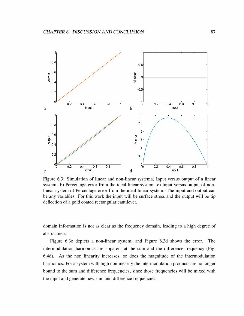
CHAPTER 6. DISCUSSION AND CONCLUSION 87
a b
c d
Figure 6.3: Simulation of linear and non-linear systema) Input versus output of a linearsystem. b) Percentage error from the ideal linear system. c) Input versus output of non-linear system d) Percentage error from the ideal linear system. The input and output canbe any variables. For this work the input will be surface stress and the output will be tipdeflection of a gold coated rectangular cantilever.
domain information is not as clear as the frequency domain, leading to a high degree of
abstractness.
Figure 6.3c depicts a non-linear system, and Figure 6.3d shows the error. The
intermodulation harmonics are apparent at the sum and the difference frequency (Fig.
6.4d). As the non linearity increases, so does the magnitude of the intermodulation
harmonics. For a system with high nonlinearity the intermodulation products are no longer
bound to the sum and difference frequencies, since those frequencies will be mixed with
the input and generate new sum and difference frequencies.

CHAPTER 6. DISCUSSION AND CONCLUSION 88
a b
a b
Figure 6.4: Two tone simulation. a) Two tone input versus time b) Two tone spectrum c)Two tone output of a non linear system c) Two tone spectrum of the output. Note the sumand difference frequencies are present in the output of the non-linear system.
6.1 Hypothesis
Two tone test provides an easy and quantitative means of measuring non linearity. Inducing
a curvature into a cantilever beam to test the hypothesis was rather challenging, which
motivated us to take a qualitative approach. Our hypothesis was due to simplification of
the beam equation for soft cantilevers. Tip deflection was no longer a linear function of
surface stress and effect of non linearity were significant and depend on the curvature of
the cantilever. For the same magnitude of surface stress, a curved cantilever would show
higher non linearity than one without curvature.

CHAPTER 6. DISCUSSION AND CONCLUSION 89
6.2 Experimental setup for two tone test
In order to induce curvature into the cantilever beam, we brought the cantilever tip close
to a microscope slide without actually touching the slide (Fig. 6.5). At close distances
between the microscope slide and cantilever the short range molecular forces act on the
soft cantilever tip and cause bending of cantilever without actually touching the glass.
We measured non-linearity vs AFM Z position of the cantilever above the slide. The
cantilever was first brought to contact and then pulled back, so that it was not in contact
(determined from vibration of tip motion). The cantilever was purchased from nano world.
The dimension of the cantilever as stated by the manufacturer were 500 µm length, 100
µm width, and 1 µm thick. There was 25 nm of gold on the top surface of the cantilever.
A custom LED were built with two distinct wavelengths. One LED operated at 420 nm
and the other at 320 nm. The LEDs were used to heat the cantilever, and each of individual
LED power could be adjusted. Due to the thermal mismatch of gold and silicon the tip
vibrated at the on off rate of each LED. Note that each LED could be turned on and off at
any rate.
6.3 Results of two tone test
Due to its small dimensions, cantilever cooling and heating was rather fast. The measured
frequency response of the cantilever vs temperature appears in Figure 6.6. We used two
frequencies 70 Hz and 150 Hz. Expecting a difference frequency of 80 Hz and a sum
frequency of 220 Hz. When the AFM Z position was pulled away only by 100 nm, as
expected we observed low amount of non linearity (Fig. 6.7). Since the AFM Z position
pulled the root of the cantilever further away from the slide surface more curvature was
experienced by the cantilever and more non linearity resulted, until the tip completely
snapped off. Figure 6.8 displays the percentage amplitude change of the tone referenced to
the input tones.

CHAPTER 6. DISCUSSION AND CONCLUSION 90
Position
Sensor
Position
LASER
Gold Coated
Cantilever
Custom LED Package
Two LED in the package
Transparent
Slide
Figure 6.5: Two tone setup to detect tip deflection due to heating by two LEDs.

CHAPTER 6. DISCUSSION AND CONCLUSION 91
Figure 6.6: Cantilever thermal frequency response. The peak at 4.6 kHz is due to theresonance frequency of the cantilever. The operating frequencies are in the flat band of theresponse.

CHAPTER 6. DISCUSSION AND CONCLUSION 92
Figure 6.7: Two tone measurement at an AFM Z height 100 nm above the slide. Note thedifference and sum frequency at 80 Hz and 220 Hz.

CHAPTER 6. DISCUSSION AND CONCLUSION 93
Figure 6.8: Percent amplitude of the tones to main excitation vs. distance of the AFM Zheight. As the Z height increases, the tip attempts to move further away from the surface,but is held in place due to surface forces and experiences higher curvature. As hypothesizedhigher non linearity occurred until the tip snapped off.
CHAPTER 6. DISCUSSION AND CONCLUSION 94
6.4 Summary of two tone test
In conclusion, these experiments demonstrate the potential of using two tone tests to
measure nonlinearities. We hypothesized the non linearities were due to curvature of
the beam. For cantilever with small tip deflection, the output is expected to be a linear
function of surface stress. However, for even small tip deflection (less than one thousandth
of the cantilever length) nonlinearities occur. These non linearities are hypothesized to
be proportional to the initial curvature of the cantilever. This technique can be used for
chemical sensing and bio-sensing using multiple films. Also cantilever curvature can be
estimated using measurements from a single point at the tip. More importantly two tone
testing reveals the interaction between films. For example, if the cantilever is coated with a
film that has a different behavior due to heat than light then the effect of light and heat can
be separated by analyzing the intermodulation products.

CHAPTER 6. DISCUSSION AND CONCLUSION 95
6.5 Conclusion
As micro mechanical systems reduce their size the new field of nano mechanics emerges.
Physical and practical issues such as lithography limit how small devices can be made.
The search for analogous functions such as actuators, sensors continues. To reduce the
device dimensions to molecular size, mechanics and chemistry must merge. We have
demonstrated that a monolayer of the aminoazobenzene MR-APTES physically exerts a
surface stress due to absorbance of a 405 nm photon, resulting in the deflection of the
tip of a micro-machined cantilever, corresponding to an average force on the order of
0.3 pN per molecule. The induced surface stress is hypothesized to be due to the trans-
cis isomerization of MR-APTES. Since this isomerization can be repeatedly induced,
averaging and Fourier techniques can be used for signal processing. The optomechanical
modulation of surface stress should enable the spectral separation of the signal of interest
from background noise sources in chemical sensors, enabling a new generation of surface
stress-based chemical sensors with improved signal to noise ratio.

Appendix A
UV LED and laser driver
For the initial testing of the azobenzene dye, a custom light emitting diode (LED) was
purchased from ST-Electronics. Two LED diodes at 432nm and 320 nm 100 µW were
custom packaged in the same enclosure with a semi hemispherical lens. The 405 nm, and
632 nm laser were purchased from Thor labs. The 405 nm Laser LP-405-SF10 came with
pig tail fiber. Since the beam at the output of the fiber behaves as point source a 405 nm
collimator was used to collimate the beam. A 632 nm collimator was also used for the
for the LP-632-SF10. The same electronics with a slight modification that was designed
to drive the LED was used to drive the laser. The block diagram of the circuit is shown
in Figure A.1a. A precision variable current source with an NMOS electrically controlled
switch was designed to turn on and off the laser or LED with an external signal generator.
A 1 Ω resistor was used to monitor the current, which represent the laser or LED light
power output. The laser light output power after the critical threshold current is directly
proportional to the current as shown from manufacturer data in Figure A.1b. For the 405
nm laser the threshold current as specified by manufacturer was 34.3 mA. We operated
the laser above 37.5 mA to ensure minimal power fluctuation. A detailed schematic of the
circuit appears in Figure A.2. The current source had better than 60 dB supply rejection and
maintained the current to better than 0.01% accuracy. The laser output power was verified
with PM-10 sensor with a Fieldmate power meter and matched the power from current
power curve of Figure A.1b within the accuracy of the meter.
96

APPENDIX A. UV LED AND LASER DRIVER 97
a
Precision Current
source
Light emitting diode
Or LASER
1 Ohm current
sense resistor
NMOS
switch
b
Figure A.1: a) Block diagram of the LED and laser driver circuit. A 20 turn potentiometerwas used to vary the current source. The 1 Ω resistor converts the current to a voltagewithout loss of headroom. The voltage across the resistor was monitored during operation.b) Manufacturer light power output of the laser measured at the fiber output. The lightoutput power of the laser is directly proportional to the current through the laser. The laseroutput power measured with PM-10 sensor and a fieldmate meter matched the power vs.current curve within the accuracy of the meter.

APPENDIX A. UV LED AND LASER DRIVER 98
Figure A.2: Detailed schematic of UV-LED and laser driver circuit. Resistor R3 waschanged to 10 Ω for laser drive application.

Appendix B
X-ray photoelectron spectrometry
X-ray Photoelectron Spectroscopy (XPS) provides surface chemical characterization capa-
bilities, probing the surface top 10 A. High surface sensitivity makes the technique ideal
for studying deposited films and verifying their composition. XPS is based on irradiation
of the sample with monochromatic xrays. The high energy photons cause ionization of
the material by direct electron emission (photoelectron) as well as secondary electron
emission (Auger)as shown in Figure B.1. Since both photoelectrons and Auger electrons
are ejected during x-ray bombardment, both are observed in XPS spectra. From the energy
of photoelectron the chemical nature of surface can be determined, also called as Electron
Spectroscopy for Chemical Analysis (ESCA).
Photoelectrons are usually scattered through a variety of inelastic processes, but some
escape the sample surface unscattered. These electrons are collected by the instrument
electron lens, analyzed according to their kinetic energy, and counted. The kinetic energy
(KE) of each photoelectron is directly proportional to the energy of the ionizing photon
and the binding energy (BE) of the corresponding atomic orbital from which the electron
was emitted, through the following relationship: KE = hv−BE. Hence each element has
a specific signature spectrum. XPS was performed on an SSI S-Probe monochromatized
x-ray photoelectron spectrometer system, with an Al (Kα) x-ray source (1486.6 eV) in an
ultra high vacuum system with a base pressure in the 10−9 Torr range. The survey scans
were collected by using a hemispherical electron energy analyzer at a pass energy of 156.5
99

APPENDIX B. X-RAY PHOTOELECTRON SPECTROMETRY 100
Figure B.1: XPS fundamentals of operation courtesy of Dr. Hitzman.
eV with 1-eV resolution. The XPS data were processed by Shirley background correction
followed by fitting to Voigt profiles. A bulk C(1s) peak at 284.6 eV was used to adjust all
of the peaks in order to correct the binding energies for the charge shift.
Appendix C
Liquid chromatography-massspectrometry
A chromatography medium consists of two components of different phases, a mobile phase
and a stationary phase. A liquid mobile phase moving over a solid stationary phase. The
stationary phase consists of an adsorbing material, such as fine grain silicon dioxide, with
diameter of less than 1 µm. The mixture is dispersed into the mobile phase, which moves
along the stationary phase. Compounds in the mixture adsorb on the stationary phase from
time to time, and then come off again. The components must be soluble in the mobile
phase, which means they have affinity for the solvent. The stationary phase is usually fairly
polar. The higher the polarity differences between the components, and the longer the
path, the more separation will occur. The acronym HPLC originally indicated the fact that
high pressure was used to generate the flow required for liquid chromatography in packed
columns.
The output of the column then is then fed to an electrospray, a device that uses high
electric field to disperse the fine aerosol as shown in Figure C.1A. The Ions are then fed
to a quadruple mass spectrometer. We found by setting the ionization voltage to 25 V in
the Waters mass spectrometer far less fragmentation occurred than at the standard setting.
We used the C18-01-LowV setting of the Waters instrument shown in Figure C.1B for all
the data presented in this report. We kept the concentration of the sample between 20-50
101

APPENDIX C. LIQUID CHROMATOGRAPHY-MASS SPECTROMETRY 102
A
B
Figure C.1: A) Electrospray block diagram. B) Photo of the Waters mass spectrometerinstrument. We used a low voltage setting to reduce fragmentation. Figure courtesy of Dr.Allis Chein.
µM, and used the least amount of organic solvent to prevent breakthrough the column. It
is also important to note that in the negative (ESI−) or positive electrospray current (ESI+)
common masses of adduct are found (Table C.1).

APPENDIX C. LIQUID CHROMATOGRAPHY-MASS SPECTROMETRY 103
ESI+ ESI−
M+H+ M−H−
M+Na+ M+Cl−
M+NH+4 M−H + f ormic acid−
2M+H+n 2M−H−
M+nHn+ M+nHn−
Table C.1: Common mass of adducts found in electrospray current. For example, in theESI− mass, of the compound (M) plus the mass of chlorine (Cl) is commonly found.
Appendix D
Matlab signal processing code
Two signal processing codes were used to filter the data. The first code called ”Post.m”
achieves the filtering described on page 77. The second code ”CycleAvg.m” uses one cycle
of the data as a matched filter.
In the post processing code Post.m note the filtering and point selection.
c l o s e a l lc l e a r a l l
%W r i t t e n by A . Joseph R a s t e g a r da ta p o s t p r o c e s s i n g
%−−−Uncomment t h e da ta f i l e −−−−−
%t h e n run t h e s c r i p t ( p r e s s F5 )
%f i l e n a m e 1 = ’ Trace ’
%f i l e n a m e 1= ’MR Cant i2−R i g h t . mat ’
%f i l e n a m e 1 = ’MR Cant i2−R i g h t . mat ’
f i l e n a m e 1 = ’ Ref c a n t i on G l a s s Try 2 . mat ’
load ( f i l e n a m e 1 )
Bandpass = . 1 ;% i n H e r t z
C e n t e r =1; % Chop Frequency
Freqend = 5 %end f r e q o f a l l t h e s p e c t r a l p l o t
l p c o r n e r = 10 %c o r n e r o f t h e low pass f i l t e r
104

APPENDIX D. MATLAB SIGNAL PROCESSING CODE 105
f i g u r ex=Vtb ;
p l o t ( t , x ) ;
t i t l e ( f i l e n a m e 1 )
%−− i n p u t p l o t i s x
f i g u r eh = s p e c t r u m . pe r iodog ram ;
psd ( h , x , ’ Fs ’ , Fs ) ;
TITLE ( f i l e n a m e 1 )
a x i s ( [ 0 Freqend −80 0 ] ) ;
%−−FFT
f i g u r em = l e n g t h ( Vtb ) ; % Window l e n g t h
NFFT = pow2 ( nextpow2 (m) ) ; % Trans form l e n g t h
fx = f f t ( x , NFFT ) /m; % DFT
f = Fs / 2 * l i n s p a c e ( 0 , 1 , NFFT / 2 + 1 ) ; % Frequency range
p l o t ( f , 1 . 4 * abs ( fx ( 1 : NFFT / 2 + 1 ) ) , ’ b ’ )
x l a b e l ( ’ F requency ( Hz ) ’ )
y l a b e l ( ’Vrms ’ )
%t i t l e ( ’\ b f Spec trum o f Vtb ’ )
t i t l e ( f i l e n a m e 1 )
a x i s ( [ . 1 Freqend 0 . 0 3 ] ) ;
f i g u r eLowpassco rne r = l p c o r n e r / Fs / 2 ;
low= ( C e n t e r / ( Fs / 2 ) ) − ( Bandpass / ( Fs / 2 ) ) ;
h igh =( C e n t e r / ( Fs / 2 ) ) + ( Bandpass / ( Fs / 2 ) ) ;
b= f i r 1 ( 2 ˆ 1 4 , [ low h igh ] ) ; %band pass f i l t e r
%b= f i r 1 ( 2 ˆ 8 , [ Lowpasscorner ] ) ; %low pass f i l t e r

APPENDIX D. MATLAB SIGNAL PROCESSING CODE 106
f r e q z ( b , 1 , 2 ˆ 1 6 , Fs )
a x i s ( [ 0 3 −80 5 ] ) ;
s u b p l o t ( 2 , 1 , 2 ) ;
a x i s ( [ 0 3 −2000 7 0 0 ] ) ;
y= f f t f i l t ( b , x ) ;
%−−o u t p u t p l o t i s y
f i g u r eS u b p l o t ( 2 , 1 , 1 ) ;
p l o t ( t , x ) ;
a x i s ( [ 0 120 −.5 . 2 ] ) ;
TITLE ( ’ F i l t e r i n p u t ’ )
v1= a x i s ;
xx=x−mean ( x ) ;
xrms= s q r t ( mean ( xx . * xx ) ) ;
t e x t ( 1 0 , v1 (4 ) − . 1 , [ ’RMS−mean i n mV= ’ num2str ( xrms * 1 0 0 0 ) ] ) ;
S u b p l o t ( 2 , 1 , 2 ) ;
p l o t ( t , y )
a x i s ( [ 0 120 −.3 . 3 ] ) ;
t i t l e ( ’ F i l t e r o u t p u t ’ ) ;
tmin =min ( t ) ;
ymax=max ( y ) ;
ymean=mean ( y ) ;
yy=y−ymean ;
yrms= s q r t ( mean ( yy . * yy ) ) ;
v= a x i s ;
t e x t ( 1 0 , v (4 ) − . 1 , [ ’RMS−mean i n mV = ’ num2str ( yrms * 1 0 0 0 ) ] ) ;
%msspec trum ( h , y , ’ Fs ’ , Fs , ’ NFFT ’ , 2 ˆ 1 4 )
s c r s z = g e t ( 0 , ’ S c r e e n S i z e ’ ) ;
%f i g u r e
APPENDIX D. MATLAB SIGNAL PROCESSING CODE 107
%( ’ P o s i t i o n ’ , [ 2 0 s c r s z (4) /2−50 s c r s z ( 3 ) / 2 s c r s z ( 4 ) / 2 −5 0 ] ) ;
h = s p e c t r u m . pe r iodog ram ;
% Cr ea te a per iodogram s p e c t r a l e s t i m a t o r .
psd ( h , y , ’ Fs ’ , Fs ) ;
% C a l c u l a t e s and p l o t s t h e two−s i d e d PSD .
a x i s ( [ 0 Freqend −80 0 ] ) ;
t i t l e ( f i l e n a m e 1 )
f i g u r e ( 3 )
The filter code CycleAvg.m
c l e a r a l lc l o s e a l lc l cc o n s t a n t s ( ) ;
f i l e n a m e 1 = ’ Ref c a n t i on G l a s s Try 2 . mat ’
f i l e n a m e 2 = ’MR Cant i2−r i g h t . mat ’
%−−−−−−−−−−−−−−−−−−−−−−−−−−−−−−−−−−−−−−−−−−−−−−−load ( f i l e n a m e 1 )
Fmod =1;
hold a l lP e r i o d = Fs / Fmod ;
t 1 = ( 1 : P e r i o d + 1 ) * 1 / Fs ;
maxCycle= l e n g t h ( t ) / Pe r iod −1;
[ a , b ]=max ( d i f f ( Vled ( 1 : P e r i o d + 1 ) ) ) ;
%The r i s i n g edge t r i g g e r from t h e l a s e r on P u l s e
S=b ;
Vseg1 =0;
APPENDIX D. MATLAB SIGNAL PROCESSING CODE 108
mean1 =0;
c y c l e =maxCycle
f o r n = 1 : c y c l e
Vseg1=Vtb ( S+( n−1)* P e r i o d : S+n* P e r i o d )+ Vseg1 ;
endm=mean ( Vseg1 ) ;
p l o t ( t1 , ( Vseg1−m) / max ( n ) , ’ . ’ )
load ( f i l e n a m e 2 )
[ a , b ]=max ( d i f f ( Vled ( 1 : P e r i o d ) ) ) ;
S=b ;
Vseg =0;
f o r n = 1 : c y c l e
Vseg=Vtb ( S+( n−1)* P e r i o d : S+n* P e r i o d )+ Vseg ;
endm=mean ( Vseg ) ;
p l o t ( t1 , ( Vseg−m) / max ( n ) , ’ . ’ )
box o f f
x l im ([− . 1 1 . 1 ] ) ;
x l a b e l ( ’ Time i n second ’ )
y l a b e l ( ’ Vo l t ’ )
p r i n t P l o t ( ’ Cycle Avg Of MR C a n t i and r e f ’ )
f i g u r ehold a l lp l o t ( 0 , 0 )
p l o t ( t ( 1 : 2 0 0 0 0 ) , Vtb ( 1 : 2 0 0 0 0 ) )
box o f f

APPENDIX D. MATLAB SIGNAL PROCESSING CODE 109
x l a b e l ( ’ Time i n second ’ )
y l a b e l ( ’ Vo l t ’ )
x l im ( [ 0 3 5 ] )
y l im ([− . 27 0 ] )
p r i n t P l o t ( ’Raw o u t p u t ’ )

Bibliography
[1] G. Binnig, C. F. Quate, and C. Gerber, “Atomic force microscope,” Physical review
letters, vol. 56, no. 9, p. 930, 1986. [Online]. Available: http://link.aps.org/doi/10.
1103/PhysRevLett.56.930http://link.aps.org/abstract/PRL/v56/p930
[2] C. Ziegler, “Cantilever-based biosensors,” Analytical and Bioanalytical Chemistry,
vol. 379, no. 7-8, pp. 946–959, Aug. 2004. [Online]. Available: http:
//www.ncbi.nlm.nih.gov/pubmed/15338089
[3] J. Stetter, “ Unpublished ook: MATERIALS AND SENSOR ARRAYS
COMPUTATIONAL EXPERIMENTAL SELECTION METHODS ... M.A. Ryan
et al., editors.”
[4] F. Battiston, “A chemical sensor based on a microfabricated cantilever array with
simultaneous resonance-frequency and bending readout,” Sensors and Actuators
B: Chemical, vol. 77, no. 1-2, pp. 122–131, Jun. 2001. [Online]. Available:
http://linkinghub.elsevier.com/retrieve/pii/S0925400501006839
[5] K. J. Albert, N. S. Lewis, C. L. Schauer, G. a. Sotzing, S. E. Stitzel,
T. P. Vaid, and D. R. Walt, “Cross-reactive chemical sensor arrays.” Chemical
reviews, vol. 100, no. 7, pp. 2595–626, Jul. 2000. [Online]. Available:
http://www.ncbi.nlm.nih.gov/pubmed/11749297
[6] L. Nicu and T. Leıchle, “Biosensors and tools for surface functionalization from
the macro-to the nanoscale: The way forward,” Journal of Applied Physics, vol.
111101, no. 2008, 2008. [Online]. Available: http://ieeexplore.ieee.org/xpls/abs all.
jsp?arnumber=4918996
110

BIBLIOGRAPHY 111
[7] R. Flores-Perez and A. Gupta, “Cantilever-based sensor for the detection of
different chromophore isomers,” Analytical . . . , vol. 79, no. 12, pp. 4702–4708,
2007. [Online]. Available: http://pubs.acs.org/doi/abs/10.1021/ac0703000
[8] R. Mukhopadhyay, V. V. Sumbayev, M. Lorentzen, J. r. Kjems, P. a. Andreasen, and
F. Besenbacher, “Cantilever sensor for nanomechanical detection of specific protein
conformations.” Nano letters, vol. 5, no. 12, pp. 2385–8, Dec. 2005. [Online].
Available: http://www.ncbi.nlm.nih.gov/pubmed/16351182
[9] J. Fritz, “Translating Biomolecular Recognition into Nanomechanics,” Science,
vol. 288, no. 5464, pp. 316–318, Apr. 2000. [Online]. Available: http:
//www.sciencemag.org/cgi/doi/10.1126/science.288.5464.316
[10] B. Ilic, “Attogram detection using nanoelectromechanical oscillators,” Journal
of Applied Physics, vol. 95, no. 7, p. 3694, 2004. [Online]. Available:
http://link.aip.org/link/?JAP/95/3694/1&Agg=doi
[11] N. Nugaeva, K. Y. Gfeller, N. Backmann, H. P. Lang, M. Duggelin, and M. Hegner,
“Micromechanical cantilever array sensors for selective fungal immobilization and
fast growth detection.” Biosensors & bioelectronics, vol. 21, no. 6, pp. 849–56,
Dec. 2005. [Online]. Available: http://www.ncbi.nlm.nih.gov/pubmed/16257652
[12] J. Barnes, R. Stephenson, and M. Welland, “Photothermal spectroscopy
with femtojoule sensitivity using a micromechanical device,” Nature,
1994. [Online]. Available: http://www.chem.ucla.edu/dept/Faculty/gimzewski/
publications/104 1994 Nature.pdf
[13] T. Thundat, S. L. Sharp, W. G. Fisher, R. J. Warmack, and E. a. Wachter,
“Micromechanical radiation dosimeter,” Applied Physics Letters, vol. 66, no. 12, p.
1563, 1995. [Online]. Available: http://link.aip.org/link/APPLAB/v66/i12/p1563/
s1&Agg=doi
[14] S. R. Manalis, S. C. Minne, C. F. Quate, G. G. Yaralioglu, and a. Atalar,
“Two-dimensional micromechanical bimorph arrays for detection of thermal

BIBLIOGRAPHY 112
radiation,” Applied Physics Letters, vol. 70, no. 24, p. 3311, 1997. [Online].
Available: http://link.aip.org/link/APPLAB/v70/i24/p3311/s1&Agg=doi
[15] J. Varesi, J. Lai, T. Perazzo, Z. Shi, and a. Majumdar, “Photothermal
measurements at picowatt resolution using uncooled micro-optomechanical
sensors,” Applied Physics Letters, vol. 71, no. 3, p. 306, 1997. [Online]. Available:
http://link.aip.org/link/APPLAB/v71/i3/p306/s1&Agg=doi
[16] J. Gimzewski, C. Gerber, E. Meyer, and R. Schlittler, “Observation of a
chemical reaction using a micromechanical sensor,” Chemical Physics Letters,
vol. 217, no. 5-6, pp. 589–594, Jan. 1994. [Online]. Available: http:
//linkinghub.elsevier.com/retrieve/pii/0009261493E1419H
[17] M. Godin, V. Tabard-Cossa, Y. Miyahara, T. Monga, P. J. Williams, L. Y. Beaulieu,
R. Bruce Lennox, and P. Grutter, “Cantilever-based sensing: the origin of surface
stress and optimization strategies.” Nanotechnology, vol. 21, no. 7, p. 75501, Feb.
2010. [Online]. Available: http://www.ncbi.nlm.nih.gov/pubmed/20081290
[18] R. Berger, “Surface Stress in the Self-Assembly of Alkanethiols on Gold,”
Science, vol. 276, no. 5321, pp. 2021–2024, Jun. 1997. [Online]. Available:
http://www.sciencemag.org/cgi/doi/10.1126/science.276.5321.2021
[19] J. Fritz, “Cantilever biosensors.” The Analyst, vol. 133, no. 7, pp. 855–63, Jul. 2008.
[Online]. Available: http://www.ncbi.nlm.nih.gov/pubmed/18575634
[20] W. Haiss, “Surface stress of clean and adsorbate-covered solids,” INSTITUTE OF
PHYSICS PUBLISHING, vol. 64, pp. 591–648, 2001.
[21] C. D. Bain, E. B. Troughton, Y. T. Tao, J. Evall, G. M. Whitesides, and
R. G. Nuzzo, “Formation of monolayer films by the spontaneous assembly
of organic thiols from solution onto gold,” Journal of the American Chemical
Society, vol. 111, no. 1, pp. 321–335, Jan. 1989. [Online]. Available:
http://pubs.acs.org/doi/abs/10.1021/ja00183a049
BIBLIOGRAPHY 113
[22] a. Loui, S. Elhadj, D. J. Sirbuly, S. K. McCall, B. R. Hart, and T. V. Ratto,
“An analytic model of thermal drift in piezoresistive microcantilever sensors,”
Journal of Applied Physics, vol. 107, no. 5, p. 054508, 2010. [Online]. Available:
http://link.aip.org/link/JAPIAU/v107/i5/p054508/s1&Agg=doi
[23] H.-F. Ji and B. D. Armon, “Approaches to increasing surface stress for improving
signal-to-noise ratio of microcantilever sensors.” Analytical chemistry, vol. 82,
no. 5, pp. 1634–42, Mar. 2010. [Online]. Available: http://www.pubmedcentral.nih.
gov/articlerender.fcgi?artid=2836585&tool=pmcentrez&rendertype=abstract
[24] H. Ibach, “The role of surface stress in reconstruction, epitaxial growth
and stabilization of mesoscopic structures,” Surface Science Reports, vol. 29,
pp. 193–263, 1997. [Online]. Available: http://scholar.google.com/scholar?
hl=en&btnG=Search&q=intitle:The+role+of+surface+stress+in+reconstruction,
+epitaxial+growth+and+stabilization+of+mesoscopic+structures#0
[25] V. Heine and L. Marks, “Competition between pairwise and multi-atom forces
at noble metal surfaces,” Surface Science, vol. 165, pp. 65–82, 1986. [Online].
Available: http://www.sciencedirect.com/science/article/pii/0039602886906643
[26] T. Yang, X. Li, Y. Chen, D.-W. Lee, and G. Zuo, “Adsorption induced surface-stress
sensing signal originating from both vertical interface effects and intermolecular
lateral interactions.” The Analyst, vol. 136, no. 24, pp. 5261–9, Dec. 2011. [Online].
Available: http://www.ncbi.nlm.nih.gov/pubmed/22010113
[27] G. G. Stoney, “The Tension of Metallic Films Deposited by Electrolysis,”
Proceedings of the Royal Society of London. Series A, Containing Papers of a
Mathematical and Physical Character (1905-1934), vol. 82, no. 553, pp. 172–175,
May 1909. [Online]. Available: http://rspa.royalsocietypublishing.org/cgi/doi/10.
1098/rspa.1909.0021
[28] G. Janssen, M. Abdalla, F. Van Keulen, B. Pujada, B. Van Venrooy, F. Vankeulen,
and B. Vanvenrooy, “Celebrating the 100th anniversary of the Stoney equation for
film stress: Developments from polycrystalline steel strips to single crystal silicon

BIBLIOGRAPHY 114
wafers,” Thin Solid Films, vol. 517, no. 6, pp. 1858–1867, Jan. 2009. [Online].
Available: http://linkinghub.elsevier.com/retrieve/pii/S0040609008007669
[29] M. Godin, V. Tabard-Cossa, P. Grutter, and P. Williams, “Quantitative surface stress
measurements using a microcantilever,” Applied Physics Letters, vol. 79, no. 4,
p. 551, 2001. [Online]. Available: http://link.aip.org/link/APPLAB/v79/i4/p551/
s1&Agg=doi
[30] V. Tabard-Cossa, M. Godin, L. Beaulieu, and P. Grutter, “A differential
microcantilever-based system for measuring surface stress changes induced by
electrochemical reactions,” Sensors and Actuators B: Chemical, vol. 107, no. 1, pp.
233–241, May 2005. [Online]. Available: http://linkinghub.elsevier.com/retrieve/
pii/S0925400504007002
[31] E. D. Langlois, G. a. Shaw, J. a. Kramar, J. R. Pratt, and D. C. Hurley, “Spring
constant calibration of atomic force microscopy cantilevers with a piezosensor
transfer standard.” The Review of scientific instruments, vol. 78, no. 9, p. 093705,
Sep. 2007. [Online]. Available: http://www.ncbi.nlm.nih.gov/pubmed/17902953
[32] E. a. Ramırez, E. Cortes, a. a. Rubert, P. Carro, G. Benıtez, M. E. Vela,
and R. C. Salvarezza, “Complex surface chemistry of 4-mercaptopyridine
self-assembled monolayers on Au(111).” Langmuir : the ACS journal of surfaces
and colloids, vol. 28, no. 17, pp. 6839–47, May 2012. [Online]. Available:
http://www.ncbi.nlm.nih.gov/pubmed/22497438
[33] R. Wang, L. Jiang, T. Iyoda, D. A. Tryk, K. Hashimoto, and A. Fujishima, “In-
vestigation of the Surface Morphology and Photoisomerization of an Azobenzene-
Containing Ultrathin Film,” Film, no. 29, pp. 2052–2057, 1996.
[34] D. M. Alloway, M. Hofmann, D. L. Smith, N. E. Gruhn, A. L. Graham, R. Colorado,
V. H. Wysocki, T. R. Lee, P. a. Lee, and N. R. Armstrong, “Interface Dipoles
Arising from Self-Assembled Monolayers on Gold: UVPhotoemission Studies
of Alkanethiols and Partially Fluorinated Alkanethiols,” The Journal of Physical

BIBLIOGRAPHY 115
Chemistry B, vol. 107, no. 42, pp. 11 690–11 699, Oct. 2003. [Online]. Available:
http://pubs.acs.org/doi/abs/10.1021/jp034665%2B
[35] B. Das and S. Abe, “Molecular switch on a metal surface.” The journal of
physical chemistry. B, vol. 110, no. 9, pp. 4247–55, Mar. 2006. [Online]. Available:
http://www.ncbi.nlm.nih.gov/pubmed/16509720
[36] S. G. Ray, H. Cohen, R. Naaman, H. Liu, and D. H. Waldeck, “Organization-induced
charge redistribution in self-assembled organic monolayers on gold.” The journal
of physical chemistry. B, vol. 109, no. 29, pp. 14 064–73, Jul. 2005. [Online].
Available: http://www.ncbi.nlm.nih.gov/pubmed/16852766
[37] H. Sellers, Y. Shnidman, J. E. Eilerss, and R. M. Langmuir, “Structure and Binding
of Alkanethiolates on Gold and Silver Surfaces: Implications for Self-Assembled
Monolayers,” Langmuir, no. 8, pp. 9389–9401, 1993.
[38] T. Nagahiro, H. Akiyama, M. Hara, and K. Tamada, “Photoisomerization
of azobenzene containing self-assembled monolayers investigated by Kelvin
probe work function measurements,” Journal of Electron Spectroscopy and Related
Phenomena, vol. 172, no. 1-3, pp. 128–133, May 2009. [Online]. Available:
http://linkinghub.elsevier.com/retrieve/pii/S0368204809000504
[39] K. Tamada, H. Akiyama, and T. X. Wei, “Photoisomerization Reaction of
Unsymmetrical Azobenzene Disulfide Self-Assembled Monolayers Studied by
Surface Plasmon Spectroscopy: Influences of Side Chain Length and Contacting
Medium,” Langmuir, vol. 18, no. 13, pp. 5239–5246, Jun. 2002. [Online]. Available:
http://pubs.acs.org/doi/abs/10.1021/la0157667
[40] R. Klajn, “Immobilized azobenzenes for the construction of photoresponsive
materials,” Pure and Applied Chemistry, vol. 82, no. 12, pp. 2247–2279, Oct. 2010.
[Online]. Available: http://iupac.org/publications/pac/82/12/2247/
[41] G. Fang, N. Koral, C. Zhu, Y. Yi, M. a. Glaser, J. E. Maclennan, N. a. Clark, E. D.
Korblova, and D. M. Walba, “Effect of concentration on the photo-orientation and
BIBLIOGRAPHY 116
relaxation dynamics of self-assembled monolayers of mixtures of an azobenzene-
based triethoxysilane with octyltriethoxysilane.” Langmuir : the ACS journal of
surfaces and colloids, vol. 27, no. 7, pp. 3336–42, Apr. 2011. [Online]. Available:
http://www.ncbi.nlm.nih.gov/pubmed/21401057
[42] F. T. Goericke and W. P. King, “Modeling Piezoresistive Microcantilever
Sensor Response to Surface Stress for Biochemical Sensors,” IEEE Sensors
Journal, vol. 8, no. 8, pp. 1404–1410, Aug. 2008. [Online]. Available:
http://ieeexplore.ieee.org/lpdocs/epic03/wrapper.htm?arnumber=4567517
[43] Y. Mo, Z. Xuan, V. Kambiz, S. O. Cengiz, M. Yang, X. Zhang, K. Vafai, and
C. S. Ozkan, “High sensitivity piezoresistive cantilever design and optimization
for analyte-receptor binding,” Journal of Micromechanics and Microengineering,
vol. 13, no. 6, p. 864, 2003. [Online]. Available: http://stacks.iop.org/0960-1317/
13/864
[44] A. J. Rastegar, M. Vosgueritchian, J. C. Doll, J. R. Mallon, and B. L. Pruitt,
“Nanomechanical actuation of a silicon cantilever using an azo dye, self-assembled
monolayer,” Langmuir, vol. 29, no. 23, pp. 7118–7124, 2013. [Online]. Available:
http://pubs.acs.org/doi/abs/10.1021/la3034676
[45] J. H. Park, P. Scheerer, K. P. Hofmann, H.-W. Choe, and O. P. Ernst,
“Crystal structure of the ligand-free G-protein-coupled receptor opsin.” Nature,
vol. 454, no. 7201, pp. 183–7, Jul. 2008. [Online]. Available: http:
//www.ncbi.nlm.nih.gov/pubmed/18563085
[46] K. P. C. Vollhardt and N. E. Schore, Organic chemistry: structure and function.
W.H. Freeman, 2005. [Online]. Available: http://books.google.com/books?id=
dWS7QgAACAAJ
[47] Y. Zhao and T. Ikeda, Smart light-responsive materials: azobenzene-containing
polymers and liquid crystals. Wiley, 2009. [Online]. Available: http://books.
google.com/books?id=pBy3vMNmwOgC
BIBLIOGRAPHY 117
[48] H. Durr and H. Bouas-Laurent, Photochromism: molecules and systems, ser.
Studies in organic chemistry. Elsevier, 1990. [Online]. Available: http:
//books.google.com/books?id=iA7wAAAAMAAJ
[49] E. Fuhrmann, “Synthesis of Alkyl Aryl Ethers by Catalytic Williamson Ether
Synthesis with Weak Alkylation Agents Abstract :,” Organic Process Research &
Development, vol. 9, no. 2, 2005.
[50] T. Gierczak, J. B. Burkholder, S. Bauerle, and a.R. Ravishankara, “Photochemistry
of acetone under tropospheric conditions,” Chemical Physics, vol. 231, no. 2-3, pp.
229–244, Jun. 1998. [Online]. Available: http://linkinghub.elsevier.com/retrieve/pii/
S0301010498000068
[51] E. V. Anslyn and D. A. Dougherty, Modern physical organic chemistry. University
Science, 2006. [Online]. Available: http://books.google.com/books?id=gY-Sxijk
tMC
[52] M. Mahmoud, “Low excitation energy band of 4-hydroxyazobenzene derivatives,”
Spectrochimica Acta Part A: Molecular Spectroscopy, vol. 39, no. 8, pp.
729–733, 1983. [Online]. Available: http://linkinghub.elsevier.com/retrieve/pii/
0584853983801196
[53] Y. Ootani, K. Satoh, A. Nakayama, T. Noro, and T. Taketsugu, “Ab initio molecular
dynamics simulation of photoisomerization in azobenzene in the n pi* state.” The
Journal of chemical physics, vol. 131, no. 19, p. 194306, Nov. 2009. [Online].
Available: http://www.ncbi.nlm.nih.gov/pubmed/19929050
[54] Y. Yi, M. J. Farrow, E. Korblova, D. M. Walba, and T. E. Furtak, “High-sensitivity
aminoazobenzene chemisorbed monolayers for photoalignment of liquid crystals.”
Langmuir : the ACS journal of surfaces and colloids, vol. 25, no. 2, pp. 997–1003,
Jan. 2009. [Online]. Available: http://www.ncbi.nlm.nih.gov/pubmed/19093815
[55] C. Barrett, A. Natansohn, and P. Rochod, “Cis-Trans Thermal Isomerization Rates
of Bound and Doped Azobenzenes in a Series of Polymers,” Society, vol. 2, no. 7,
pp. 899–903, 1995.

BIBLIOGRAPHY 118
[56] N. J. Dunn, W. H. Humphries, A. R. Offenbacher, T. L. King, and J. a. Gray,
“pH-Dependent cis –¿ trans isomerization rates for azobenzene dyes in aqueous
solution.” The journal of physical chemistry. A, vol. 113, no. 47, pp. 13 144–51,
Nov. 2009. [Online]. Available: http://www.ncbi.nlm.nih.gov/pubmed/19618926
[57] K. Tamada, J. Nagasawa, F. Nakanishi, K. Abe, T. Ishida, M. Hara, and
W. Knoll, “Structure and Growth of Hexyl Azobenzene Thiol SAMs on Au(111),”
Langmuir, vol. 14, no. 12, pp. 3264–3271, Jun. 1998. [Online]. Available:
http://pubs.acs.org/doi/abs/10.1021/la971348j
[58] K. Moriwaki, M. Kusumoto, K. Akamatsu, H. Nakano, and Y. Shirota, “Kazuyuki
Moriwaki, Mitsushi Kusumoto, Keiichi Akamatsu, Hideyuki Nakano and Yasuhiko
Shirota*,” pp. 2671–2676, 1998.
[59] P. Dietrich, F. Michalik, R. Schmidt, C. Gahl, G. Mao, M. Breusing,
M. B. Raschke, B. Priewisch, T. Elsasser, R. Mendelsohn, M. Weinelt, and
K. Ruck-Braun, “An anchoring strategy for photoswitchable biosensor technology:
azobenzene-modified SAMs on Si(111),” Applied Physics A, vol. 93, no. 2, pp.
285–292, Jul. 2008. [Online]. Available: http://www.springerlink.com/index/10.
1007/s00339-008-4828-0
[60] J. Reisch, A. Wickramasinghe, and W. Probst, “Natural product chemistry, part 136:
A convenient synthesis of rutacridone and isorutacridone,” Monatshefte fr Chemie
Chemical Monthly, vol. 121, no. 10, pp. 829–835, Oct. 1990. [Online]. Available:
http://www.springerlink.com/index/10.1007/BF00808376
[61] R. Pena Alonso, F. Rubio, J. Rubio, and J. L. Oteo, “Study of the hydrolysis and
condensation of γ-Aminopropyltriethoxysilane by FT-IR spectroscopy,” Journal of
Materials Science, vol. 42, no. 2, pp. 595–603, Nov. 2006. [Online]. Available:
http://www.springerlink.com/index/10.1007/s10853-006-1138-9
[62] a. F. Scott, J. E. Gray-Munro, and J. L. Shepherd, “Influence of coating bath
chemistry on the deposition of 3-mercaptopropyl trimethoxysilane films deposited
on magnesium alloy.” Journal of colloid and interface science, vol. 343, no. 2,

BIBLIOGRAPHY 119
pp. 474–83, Mar. 2010. [Online]. Available: http://www.ncbi.nlm.nih.gov/pubmed/
20064643
[63] A. Ulman, An introduction to ultrathin organic films: from Langmuir-Blodgett to
self-assembly. Academic Press, 1991. [Online]. Available: http://books.google.
com/books?id=uwTFQgAACAAJ
[64] R. Walsh, “Bond Dissociation Energy Values in Silicon-Containing Compounds asn
some of their implications,” Society, vol. 1537, no. 4, pp. 246–252, 1981.
[65] R. Merrifield, “Solid phase peptide synthesis. I. The synthesis of a tetrapeptide,”
Journal of the American Chemical Society, pp. 2149–2154, 1963. [Online].
Available: http://pubs.acs.org/doi/abs/10.1021/ja00897a025
[66] A. Ulman, “Formation and Structure of Self-Assembled Monolayers.” Chemical
reviews, vol. 96, no. 4, pp. 1533–1554, Jun. 1996. [Online]. Available:
http://www.ncbi.nlm.nih.gov/pubmed/11848802
[67] I. Halter, “Covalently Attached Organic Monolayers on Semiconductor Surfaces,”
Journal of the American Chemical Society, pp. 8050–8055, 1978.
[68] J. Kim, P. Seidler, L. S. Wan, and C. Fill, “Formation, structure, and reactivity
of amino-terminated organic films on silicon substrates.” Journal of colloid and
interface science, vol. 329, no. 1, pp. 114–9, Jan. 2009. [Online]. Available:
http://www.ncbi.nlm.nih.gov/pubmed/18930465
[69] J. a. Howarter and J. P. Youngblood, “Optimization of silica silanization
by 3-aminopropyltriethoxysilane.” Langmuir : the ACS journal of surfaces and
colloids, vol. 22, no. 26, pp. 11 142–7, Dec. 2006. [Online]. Available:
http://www.ncbi.nlm.nih.gov/pubmed/17154595
[70] E. M. E. Kristensen, F. Nederberg, H. k. Rensmo, T. Bowden, J. Hilborn,
and H. Siegbahn, “Photoelectron spectroscopy studies of the functionalization
of a silicon surface with a phosphorylcholine-terminated polymer grafted
onto (3-aminopropyl)trimethoxysilane.” Langmuir : the ACS journal of surfaces

BIBLIOGRAPHY 120
and colloids, vol. 22, no. 23, pp. 9651–7, Nov. 2006. [Online]. Available:
http://www.ncbi.nlm.nih.gov/pubmed/17073492
[71] J. Kim, J. Cho, P. M. Seidler, N. E. Kurland, and V. K. Yadavalli, “Investigations
of chemical modifications of amino-terminated organic films on silicon substrates
and controlled protein immobilization.” Langmuir : the ACS journal of surfaces
and colloids, vol. 26, no. 4, pp. 2599–608, Feb. 2010. [Online]. Available:
http://www.ncbi.nlm.nih.gov/pubmed/20095550
[72] J. A. Maurer, K. D. Moeller, J.-s. Taylor, K. Wooley, and C. A. Schlecht, “by In the
unlikely event that the author did not send a complete manuscript,” no. May 2009.
[73] J. R. Mallon, a. J. Rastegar, a. a. Barlian, M. T. Meyer, T. H. Fung, and B. L.
Pruitt, “Low 1f noise, full bridge, microcantilever with longitudinal and transverse
piezoresistors,” Applied Physics Letters, vol. 92, no. 3, p. 033508, 2008. [Online].
Available: http://link.aip.org/link/APPLAB/v92/i3/p033508/s1&Agg=doi
[74] B. W. Chui, T. D. Stowe, T. W. Kenny, H. J. Mamin, B. D. Terris, and D. Rugar,
“Low-stiffness silicon cantilevers for thermal writing and piezoresistive readback
with the atomic force microscope,” Applied Physics Letters, vol. 69, no. 18, pp.
2767–2769, 1996. [Online]. Available: http://link.aip.org/link/?APL/69/2767/1
[75] J. A. Harley and T. W. Kenny, “1/f noise considerations for the design
and process optimization of piezoresistive cantilevers,” Microelectromechanical
Systems, Journal of, vol. 9, no. 2, pp. 226–235, 2000.
[76] B. L. Pruitt, W.-t. Park, and T. W. Kenny, “Measurement system for low force and
small displacement contacts,” Microelectromechanical Systems, Journal of, vol. 13,
no. 2, pp. 220–229, 2004.
[77] X. Yu, J. Thaysen, O. Hansen, a. Boisen, and I. Introduction, “Optimization
of sensitivity and noise in piezoresistive cantilevers,” Journal of Applied Physics,
vol. 92, no. 10, pp. 6296–6301, 2002. [Online]. Available: http://link.aip.org/link/
?JAP/92/6296/1http://link.aip.org/link/JAPIAU/v92/i10/p6296/s1&Agg=doi

BIBLIOGRAPHY 121
[78] A. A. Davenport, P. Lim, and B. Pruitt, “IMECE2005-81590 Noise Studies in
Implanted Piezoresistors,” Electrical Engineering, 2005.
[79] A. A. Barlian, S.-J. Park, V. Mukundan, and B. L. Pruitt, “Design and
characterization of microfabricated piezoresistive floating element-based shear
stress sensors,” Sensors and Actuators A: Physical, vol. 134, no. 1, pp.
77–87, 2007. [Online]. Available: http://www.sciencedirect.com/science/article/
B6THG-4K4WMR5-1/2/824b1bd434ab12ef52281798a3daf62d
[80] A. Kurtz, J. Mallon, and T. Nunn, “Pressure transducers exhibiting linear
pressure operation,” Oct. 16 1984, uS Patent 4,476,726. [Online]. Available:
http://www.google.com/patents/US4476726
[81] M. Hopcroft and W. Nix, “What is the Young’s Modulus of Silicon?”
Systems, Journal of, vol. 19, no. 2, pp. 229–238, 2010. [Online]. Available:
http://ieeexplore.ieee.org/xpls/abs all.jsp?arnumber=5430873
[82] W. G. Pfann and R. N. Thurston, “Semiconducting Stress Transducers
Utilizing the Transverse and Shear Piezoresistance Effects,” Journal of Applied
Physics, vol. 32, no. 10, pp. 2008–2019, 1961. [Online]. Available: http:
//link.aip.org/link/?JAP/32/2008/1
[83] M. Tortonese, “Force sensors for scanning probe microscopy,” Ph.D. dissertation,
1993.
[84] X. Yu, Y. Tang, H. Zhang, T. Li, and W. Wang, “Design of High-
Sensitivity Cantilever and Its Monolithic Integration With CMOS Circuits,” Sensors
(Peterborough, NH), vol. 7, no. 4, pp. 489–495, 2007.
[85] F. N. Hooge, “l / f Noise Sources,” Physica B, vol. 41, no. 11, pp. 1926–1935, 1994.
[86] F. N. Hooge, T. G. M. Kleinpenning, and L. K. J. Vandamme, “Experimental studies
on l/f noise,” Reports on Progress in Physics, vol. 44, no. December 1980, pp. 479–
532, 1981.

BIBLIOGRAPHY 122
[87] L. K. J. Vandamme and S. Oosterhoff, “Annealing of ion-implanted resistors
reduces the 1/ f noise,” Journal of Applied Physics, vol. 59, no. 9, pp. 3169–3174,
1986. [Online]. Available: http://link.aip.org/link/?JAP/59/3169/1
[88] L. K. J. Vandamme and G. Trefan, “1/f noise in homogeneous and inhomogeneous
media,” Circuits, Devices and Systems, IEE Proceedings-, vol. 149, no. 1, pp. 3–12,
2002.
[89] R. P. Agarwal, A. Ambrozy, and H. L. Hartnagel, “Excess noise in semiconducting
BaSrTiO¡inf¿3¡/inf¿,” Electron Devices, IEEE Transactions on, vol. 24, no. 12, pp.
1337–1341, 1977.
[90] D. M. Fleetwood and N. Giordano, “Resistivity dependence of 1/f noise in metal
films,” Physical Review B, vol. 27, no. 2, p. 667, 1983. [Online]. Available:
http://link.aps.org/abstract/PRB/v27/p667
[91] E. P. Vandamme and L. K. J. Vandamme, “Current crowding and its e ect on 1af
noise and third harmonic distortion a case study for quality assessment of resistors,”
Microelectronics Reliability, vol. 40, pp. 1847–1853, 2000.
[92] G. Yoshikawa, “Mechanical analysis and optimization of a microcantilever sensor
coated with a solid receptor film,” Applied Physics Letters, vol. 98, no. 17,
p. 173502, 2011. [Online]. Available: http://link.aip.org/link/APPLAB/v98/i17/
p173502/s1&Agg=doi
[93] S. Park, A. Rastegar, and J. Mallon, “Ion implanted
piezoresistive cantilever design and performance,” Proc. Solid
State Sens., . . . , no. C, pp. 98–101, 2008. [Online]. Available:
http://svn.sfu.ca/files/research/bba19/contents/Literature/Conferenceprocedings/
HiltonHead08workshop/HiltonHead2008/PDFs/Papers/028 0127.pdf
[94] Y. Zhang, Q. Ren, and Y.-p. Zhao, “Modelling analysis of surface stress on a
rectangular cantilever beam,” Journal of Physics D: Applied Physics, vol. 37, no. 15,
pp. 2140–2145, Aug. 2004. [Online]. Available: http://stacks.iop.org/0022-3727/
37/i=15/a=014?key=crossref.8d0f70e209ef93e60dc01add39430150

BIBLIOGRAPHY 123
[95] M. Z. Ansari, C. Cho, and G. Urban, “Stepped piezoresistive microcantilever
designs for biosensors,” Journal of Physics D: Applied Physics, vol. 45, no. 21, p.
215401, May 2012. [Online]. Available: http://stacks.iop.org/0022-3727/45/i=21/
a=215401?key=crossref.dcf7eb39ddd19ecca95ab5230d64ad26
[96] S. D. Senturia, Microsystem design. Kluwer Academic Publishers, 2001. [Online].
Available: http://books.google.com/books?id=G3e3NUV9qu4C
[97] P. L. Hoa, G. Suchaneck, and G. Gerlach, “Influence of polycrystalline silicon as
electrical shield on reliability and stability of piezoresistive sensors,” Sensors and
Actuators A: Physical, vol. 120, no. 2, pp. 567–572, May 2005. [Online]. Available:
http://linkinghub.elsevier.com/retrieve/pii/S0924424705000294
[98] H. Nyquist, “Thermal agitation of electric charge in conductors,”
Physical Review, vol. 32, no. 1, pp. 110–113, 1928. [Online].
Available: http://www.cs.cmu.edu/afs/cs/Web/People/sensing-sensors/readings/
available only to currently registered students/nyquist-p110 1.pdf
[99] L. K. J. Vandamme and F. N. Hooge, “What Do We Certainly Know About 1,”
vol. 55, no. 11, pp. 3070–3085, 2008.
[100] L. K. J. Vandamme and G. Trefan, “noise in homogeneous and inhomogeneous
media,” Vital And Health Statistics. Series 20 Data From The National Vitalstatistics
System Vital Health Stat 20 Data Natl Vital Sta, 1987.
[101] C. Ciofi and B. Neri, “Low-frequency noise measurements as a characterization tool
for degradation phenomena in solid-state,” October, vol. 33, 2000.
[102] L. Vandamme, “Noise as a diagnostic tool for quality and reliability of electronic
devices,” IEEE Transactions on Electron Devices, vol. 41, no. 11, pp. 2176–2187,
1994. [Online]. Available: http://ieeexplore.ieee.org/lpdocs/epic03/wrapper.htm?
arnumber=333839
[103] L. K. J. Vandamme, “Bulk and surface 1/f noise,” Electron Devices, IEEE
Transactions on, vol. 36, no. 5, pp. 987–992, 1989.

BIBLIOGRAPHY 124
[104] a. A. Barlian, W.-T. Park, J. R. Mallon, A. J. Rastegar, and B. L. Pruitt,
“Review: Semiconductor Piezoresistance for Microsystems.” Proceedings of the
IEEE. Institute of Electrical and Electronics Engineers, vol. 97, no. 3, pp. 513–552,
Jan. 2009. [Online]. Available: http://www.pubmedcentral.nih.gov/articlerender.
fcgi?artid=2829857&tool=pmcentrez&rendertype=abstract
[105] F. N. Hooge, “1/f noise is no surface effect,” Physics Letters, vol. 29, no. 3, pp.
139–140, 1969. [Online]. Available: http://www.sciencedirect.com/science/article/
B6TVM-46MM3H2-D5/2/ae4af5aa98cb9fc56fb5ab54e44cd2cb
[106] ——, “DISCUSSION OF RECENT EXPERIMENTS ON 1/f NOISE,”
Physica, vol. 60, no. 1, pp. 130–144, 1972. [Online]. Available:
http://caslon.stanford.edu:3210/sfxlcl3?sid=google;auinit=FN;aulast=Hooge;atitle=
Discussionofrecentexperimentson1/fnoise;title=PhysicaA;volume=60;issue=1;
date=1972;spage=130;issn=0378-4371
[107] B. Neri, C. Ciofi, and V. Dattilo, “Noise and Fluctuations in,” Power, vol. 44, no. 9,
pp. 1454–1459, 1997.
[108] N. Burnham, X. Chen, C. Hodges, and G. Matei, “Comparison of calibration
methods for atomic-force microscopy cantilevers,” Nanotechnology, vol. 14, pp.
1–6, 2003. [Online]. Available: http://iopscience.iop.org/0957-4484/14/1/301
[109] M. J. Higgins, R. Proksch, J. E. Sader, M. Polcik, S. Mc Endoo, J. P. Cleveland,
and S. P. Jarvis, “Noninvasive determination of optical lever sensitivity in atomic
force microscopy,” Review of Scientific Instruments, vol. 77, no. 1, p. 013701, 2006.
[Online]. Available: http://link.aip.org/link/RSINAK/v77/i1/p013701/s1&Agg=doi
[110] J. E. Sader, “Surface stress induced deflections of cantilever plates
with applications to the atomic force microscope: V-shaped plates,”
Journal of Applied Physics, vol. 89, no. 11, p. 2911, 2002. [Online].
Available: http://link.aip.org/link/JAPIAU/v89/i5/p2911/s1&Agg=doihttp://link.
aip.org/link/JAPIAU/v91/i11/p9354/s1&Agg=doi
BIBLIOGRAPHY 125
[111] P. Attard, T. Pettersson, and M. W. Rutland, “Thermal calibration of photodiode
sensitivity for atomic force microscopy,” Review of Scientific Instruments, vol. 77,
no. 11, p. 116110, 2006. [Online]. Available: http://link.aip.org/link/RSINAK/v77/
i11/p116110/s1&Agg=doi
[112] N. Umeki, T. Yoshizawa, Y. Sugimoto, T. Mitsui, K. Wakabayashi, and S. Maruta,
“Incorporation of an Azobenzene Derivative into the Energy Transducing Site
of Skeletal Muscle Myosin Results in Photo- Induced Conformational Changes,”
Changes, vol. 846, pp. 839–846, 2004.
[113] J. Gordon, “Radiation forces and momenta in dielectric media,” Physical Review A,
vol. 8, 1973. [Online]. Available: http://onlinelibrary.wiley.com/doi/10.1002/cbdv.
200490137/abstracthttp://pra.aps.org/abstract/PRA/v8/i1/p14 1
[114] Y. Yi, G. Fang, J. E. Maclennan, N. a. Clark, J. Dahdah, T. E. Furtak, K. Kim, M. J.
Farrow, E. Korblova, and D. M. Walba, “Dynamics of cis isomers in highly sensitive
amino-azobenzene monolayers: The effect of slow relaxation on photo-induced
anisotropy,” Journal of Applied Physics, vol. 109, no. 10, p. 103521, 2011. [Online].
Available: http://link.aip.org/link/JAPIAU/v109/i10/p103521/s1&Agg=doi