nanoeducator ii 2011
TRANSCRIPT
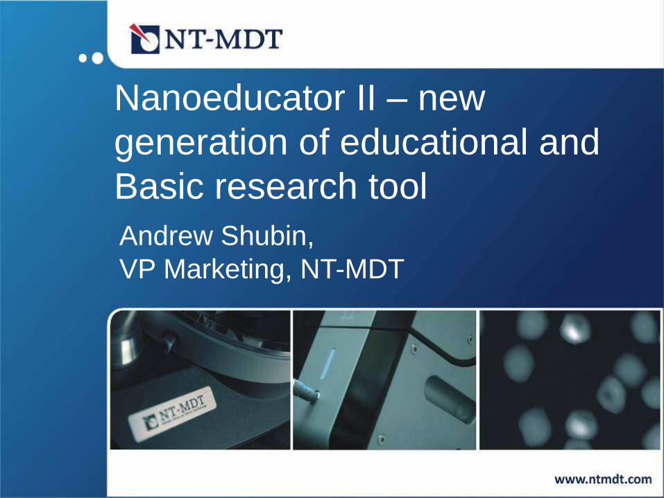
Nanoeducator II – new
generation of educational and
Basic research tool
Andrew Shubin,
VP Marketing, NT-MDT

History and Background
• 20 years on the SPM market
• Over 3800 devices in 59 countries
• 250 experts in HQ offices
• 30+ distributors worldwide

Our mission
“To enable scientists
to conduct nanoscale research
by creating advanced
instruments for nanotechnology”
Professor Victor Bykov
NT-MDT Founder and
General Manager

World-wide Distribution

NT-MDT Head Office,Moscow, Russia
NT-MDT S&LLimerick, Ireland
NT-MDT AmericaSanta Clara, USA
NT-MDT ShanghaiShanghai, China
NT-MDT EuropeEindhoven, NL
Global Representation
Representative
Offices
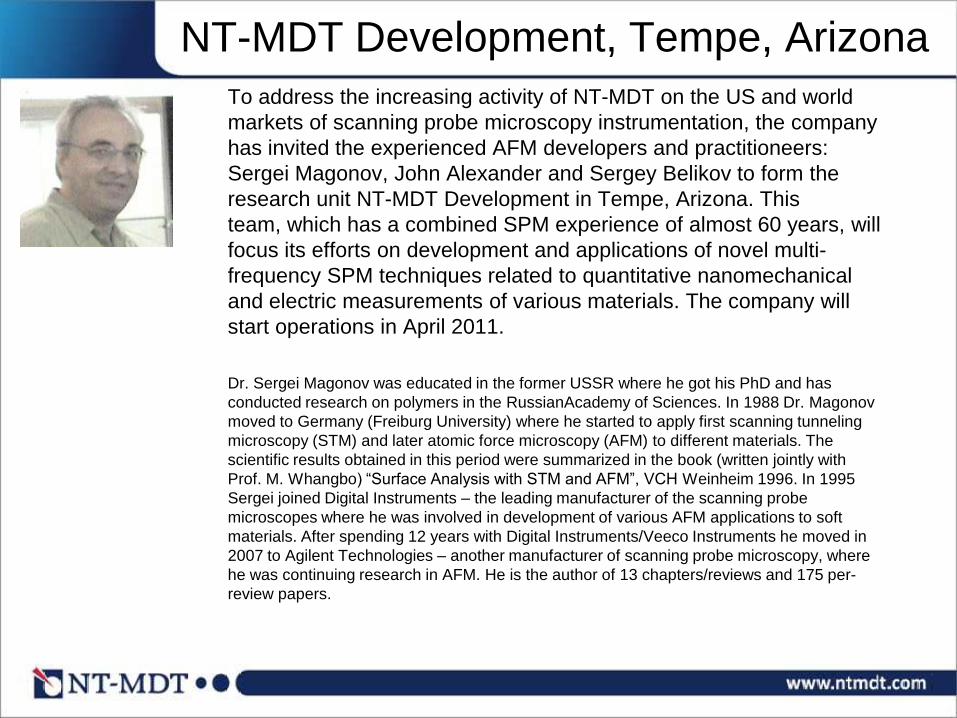
NT-MDT Development, Tempe, Arizona
To address the increasing activity of NT-MDT on the US and world
markets of scanning probe microscopy instrumentation, the company
has invited the experienced AFM developers and practitioneers:
Sergei Magonov, John Alexander and Sergey Belikov to form the
research unit NT-MDT Development in Tempe, Arizona. This
team, which has a combined SPM experience of almost 60 years, will
focus its efforts on development and applications of novel multi-
frequency SPM techniques related to quantitative nanomechanical
and electric measurements of various materials. The company will
start operations in April 2011.
Dr. Sergei Magonov was educated in the former USSR where he got his PhD and has
conducted research on polymers in the RussianAcademy of Sciences. In 1988 Dr. Magonov
moved to Germany (Freiburg University) where he started to apply first scanning tunneling
microscopy (STM) and later atomic force microscopy (AFM) to different materials. The
scientific results obtained in this period were summarized in the book (written jointly with
Prof. M. Whangbo) “Surface Analysis with STM and AFM”, VCH Weinheim 1996. In 1995
Sergei joined Digital Instruments – the leading manufacturer of the scanning probe
microscopes where he was involved in development of various AFM applications to soft
materials. After spending 12 years with Digital Instruments/Veeco Instruments he moved in
2007 to Agilent Technologies – another manufacturer of scanning probe microscopy, where
he was continuing research in AFM. He is the author of 13 chapters/reviews and 175 per-
review papers.
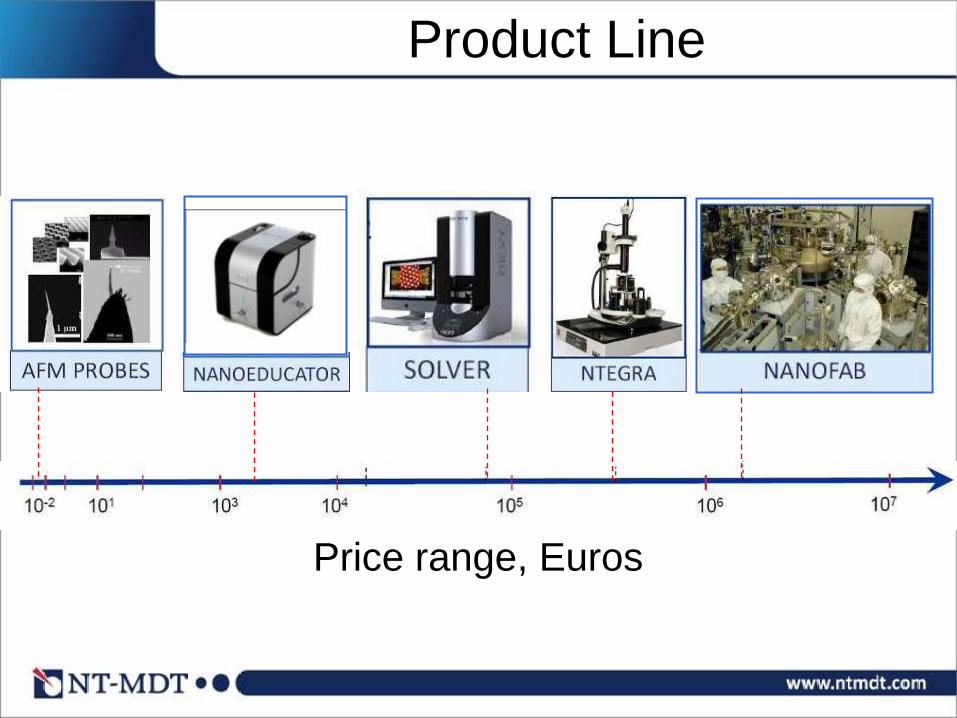
Product Line
Price range, Euros

New generation
of scientific training
laboratories
for nanotechnology
NANOEDUCATOR II
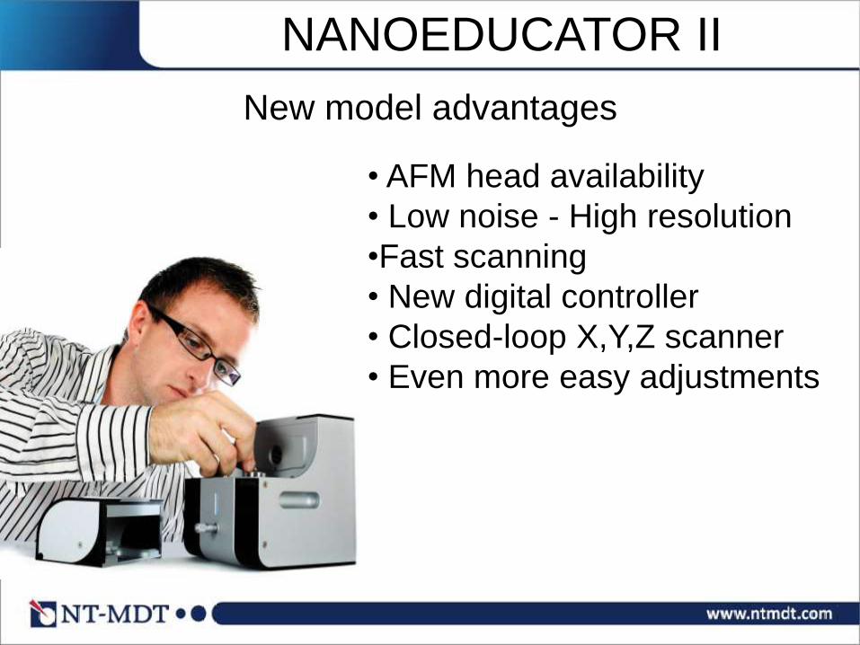
NANOEDUCATOR II
• AFM head availability
• Low noise - High resolution
•Fast scanning
• New digital controller
• Closed-loop X,Y,Z scanner
• Even more easy adjustments
New model advantages

TWO Measuring HEADS
Force Probe Head – for educational purposes
The force-probe is a piezo-tube driven into oscillation by a sinewave voltage applied to two electrodes
(inverse piezo-effect) and the oscillation amplitude is measured by the voltage generated across the
other two electrodes (direct piezo-effect).
AFM head – for the research purposes
Semiconductor laser-photodiode registration
system

Technical characteristics
Sample positioning
range:
5×5 mm
Sample positioner type: manual
Sample weight: up to 40 g
Sample size: Diameter up to 25 mm,
Thickness up to 10 mm
Scanning: Scanning by sample
Scanning range: 100×100×10 µm
(closed- loop)
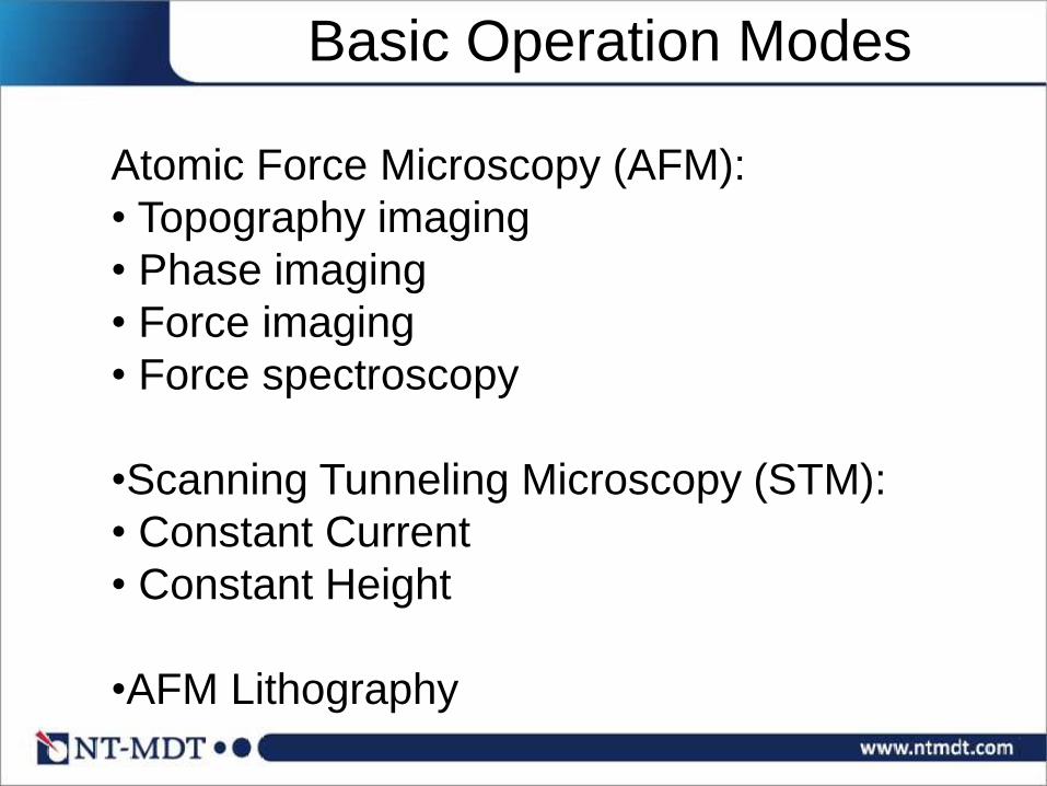
Basic Operation Modes
Atomic Force Microscopy (AFM):
• Topography imaging
• Phase imaging
• Force imaging
• Force spectroscopy
•Scanning Tunneling Microscopy (STM):
• Constant Current
• Constant Height
•AFM Lithography
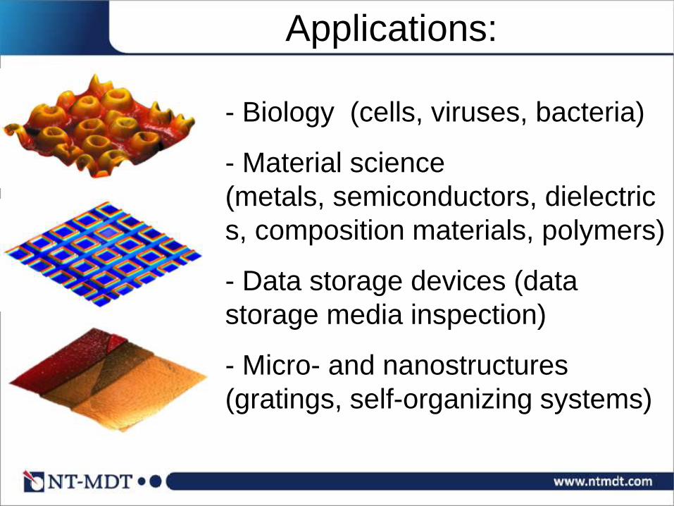
Applications:
- Biology (cells, viruses, bacteria)
- Material science
(metals, semiconductors, dielectric
s, composition materials, polymers)
- Data storage devices (data
storage media inspection)
- Micro- and nanostructures
(gratings, self-organizing systems)

Hi resolution possibilities
Sample HOPG
Scan size 2x2 nm
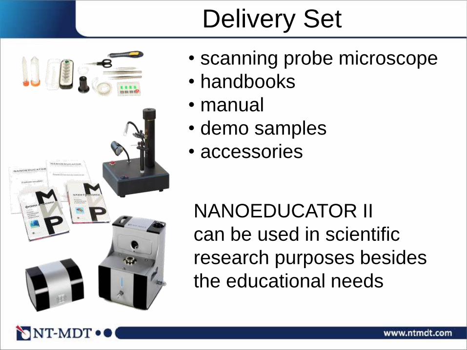
Delivery Set
NANOEDUCATOR II
can be used in scientific
research purposes besides
the educational needs
• scanning probe microscope
• handbooks
• manual
• demo samples
• accessories

Nanoeducator class

Student oriented
• User friendly interface
• Step-by-step mastering of SPM techniques
• Clear, animated support
• Inexpensive consumable materials
• Simple probe replacement
• Probe recovery availability

• New updated for operating
systems Windows® and Mac®
OS
• Remote control from the
teacher’s workstation for entire
classroom
• Various programs for image
processing and STM
manipulations
• Data sharing via iPhoneTM
and iPadTM
• Control via Internet
Cutting-Edge Tendencies

ELECTROCHEMICAL REACTION
Observing through the webcam, the tip sharpening action give the
students an insight to a common electrochemical process.
19
The etching process
The Tip Etching Device

Etching tool

Strong client support system
• Information support
• After sales service
• Ask-online service
Thank you!
YOU ARE WELCOME TO
VISIT OUR BOOTH 959