name my end of year 8 target = teacher - olsjdt · · 2013-07-071. to learn about how output...
TRANSCRIPT

Our Lady & St John Catholic CollegeO
LSJ
Des
ign
& T
echn
olog
y –
Ele
ctro
nic
Pro
duct
s
Name________________________ My end of year 8 Target = _____ Teacher _________
The ‘ Decision Maker’
WeekLesson Objectives –What will you learn about today?
Effort RatingABCDEFG
HomeworkABCDEFG
11. Circuit Symbols and circuit diagram2. Drilling and soldering Push Switch to wire
21. The diode, it’s purpose and how to identify it. 2. Resistors, values, colour bands, how to read
them.
3
1. Capacitors – Their purpose, types, how to identify
2. Switches – Types of switches and their uses in electronic products
41. 555 timer Integrated Circuits – Pins/ 2. To learn about soldering ‘I.C Sockets’ to PCB
5
1. To learn about how output components switch on and off by a 555 timer
2. To learn about quality assurance in project work
61. To learn about testing a completed circuit2. To Learn about the ‘Photo Etching’ method
for making a PCB
71. Learn how to use the vacuum forming
process to make a case2. How to assemble a product and add ‘decals’
8 1. End of Module Assessment2. Review Project Plan / How did you do?
Overall Progress 1 2 3 Overall EffortA B C D E F G
OrganisationA B C D E F G
Overall%
CWL
Awarded

The decision maker is a‘555 astable circuit and requires several electronic components to work. The symbols for all them are shown here.
Use your knowledge to write in the correct name for each symbol
Now complete the circuit diagram below by adding all the missing wires.
Use a ruler to keep your lines straight Use a pencil to draw diagrams
To make the push switch I _______________________________________________________________________________________________________________________________________
Success 4 CBA 5CBA 6CBA

Preparing the soldering iron:
Place the soldering iron in its stand and plug in. The iron will take a few minutes to reach its operating temperature of about _______°C.
Dampen the sponge in the stand. The best way to do this is to lift it out the stand and hold it under a _____ tap for a moment, then squeeze to remove ________ water. It should be ______, not dripping wet.
Wait a few minutes for the soldering iron to warm up. You can check if it is ready by trying to ______ a little solder on the ______.
Wipe the tip of the iron on the damp sponge. This will clean the tip.
Melt a little solder on the tip of the iron. This is called __________ and it will help the _____ to flow from the iron's tip to the _______. It only needs to be done when you ______ in the iron, and occasionally while soldering if you need to ______ the tip clean on the _________.
Name the 6 items from the tool Cupboard
Word Bank
400 damp excess melt
tinning heat plug Joint
Wipe sponge cold tipSuccess
4 CBA 5CBA 6CBA

Component Soldering :Hold the soldering iron like a pen, near the base of the handle. Imagine you are going to write your name! Remember to never touch the hot element or tip.
Touch the soldering iron onto the joint to be made. Make sure it touches both the component lead and the track. Hold the tip there for a few seconds and...
Feed a little solder onto the joint. It should flow smoothly onto the lead and track to form a volcano shape as shown in the diagram. Apply the solder to the joint, not the iron. The smoke is the acid from the flux inside the solder wire
Remove the solder, then the iron, while keeping the joint still. Allow the joint a few seconds to cool before you move the circuit board. If you burn your finger then put it under cold running water immediately
Inspect the joint closely. It should look shiny and have a 'volcano' shape. If not, you will need to reheat it and feed in a little more solder. This time ensure that both the lead and track are heated fully before applying solder
How do you hold a soldering iron?________________________________________How long do you hold the iron onto the joint before you add solder?________________________________________What shape should the soldered joint be?________________________________________Where does the smoke come from?________________________________________What should you wear to protect the smoke from going in your eyes?_________________________________________What do you do if the soldered joint is not the correct shape?__________________________________________What should you do if you burn your finger?__________________________________________
Label the diagram
Success
4 CBA 5CBA 6CBA

Year 8
A diode allows current to flow through it in _______ direction. Current can only flow through it from the ______ to the ________ . A diode prevents any _________ voltage caused by putting the _________ in backwards.
Label up the legs on real life picture of the DiodeAnode Cathode
Summary Questions
1.What is the name of the negative terminal of a diode? ________
2 Give one characteristic of a diode __________________
3. How can you tell the positive end of a diode?____________
4.Redraw the real life picture and the circuit symbol for a diode
5. What is a diode used for in an electronic circuit?
The Diode
Cathode
Anode
Sym
bol
Silver Band
Circuit A Circuit B
In which circuit would the bulb light up
Circuit A
Circuit B
Anode one batteries cathode reverse negative
Success
4 C B A 5 C B A 6 C B A

4CBA – 3 correct / good attempt) 5CBA – All Values with symbols 6CBA – All values and simplify using prefix ( K, M)
Success
First band = Brown = 1Second band = Grey = 8Third band = Brown = One zeroValue of resistor = 180 ohms
First band = Brown = 1Second band = Black = 0
Third band = Green = 6 zerosValue of resistor = 1,0,000000
1 Million Ohms ( 1M ohms)

4CBA (Good attempt requiring some assistance) 5CBA (Good explanations / largely correct) 6CBA (Clear and confident)
Success

Cross-out the wrong answer in the statements below
• An electrolytic capacitor is also known as a polarised/non-polarised capacitor
• The long lead (leg) of a polarised capacitor is called the cathode/anode or the positive/negative lead
• The short lead (leg) of a polarised capacitor is called the cathode/anode or the positive/negative lead
• For quality assurance purposes, a black sleeve is placed on the cathode/anode and a red sleeve on the anode/cathode.
• Label the anode and the cathode on the real life electrolytic capacitor picture
Capacitors store charge / voltage. The two types of capacitors you have used in your circuit are the ________________ and the __________________
Name three other components you have used in your circuit which are polarised. _______________ , _______________ , and ___________________.
What is the difference between the symbol of a polarised and non-polarised capacitor? _______________________________________________ _______________________________________________
Redraw the symbols for both a polarised capacitor and a battery. Clearly show the difference between them
BatteryPolarised capacitor
Symbol for Non-polarised or non-electrolytic capacitor
Symbol for a polarised or electrolytic capacitor
CAPACITORS
Electric, electrolytic, non-electric, non-electrolytic
Real life picture for a polarised or electrolytic capacitor
• The unit for measuring capacitance is
(a) current (b) volts (c) ohms• One Farad (1F) =
(a) 100 (b) 1 thousand (c) 1 million microfarads (µF)
Real Life picture of a Non- polarised or non- electrolytic capacitor
Working Level:- 4A Required significant help to complete; 5B Largely completed following teachers explanation; 6C Confidently completed with good responses
Success

SWITCHES
How well did you do? 4 CBA 5CBA 6CBA
Year 8
A switch will either stop or change the direction of current flowing in a circuit. When switches are used to control current flowing in circuits they can be made to make or break a path.
1. Identify and match the switches with the symbols. (ONE HAS BEEN DONE FOR YOU)
Name of switch
Symbol of Switch
Picture of Switch
Description
A
B
C
D
E Double pole double throw toggle switch(DPDT switch)
You are the now the Electronics Engineer!Instructions:1. You need to design a circuit that will turn a light on and off in the hallway of a new office building.2. Build a working circuit with just a battery and a bulb.
Circuit Design
Circuit design with switch included
Draw battery symbol
Draw a bulb symbol
Draw a Toggleswitch symbol
red
black
Single pole single throw toggle switch(SPST switch)
Single pole double throw micro switch(DPST switch)
Push-to-Break(PTB switch)
Double pole double throw toggle switch(DPDT switch)
Push-to-Make(PTM switch)
3. Next, add a switch in such a way that a switch turns can be included to turn the bulb on and off.
4. Name some electronic products that use ‘Push to make’ switches that could be found at school / home
Success

Year 8
Success
4 CBA 5CBA 6CBA

Label Each part of the diagram above using the correct terms below:-PCB Board, Heads LED, Tails LED, Pin 1, Negative Rail,Timing Components R1, R2, C1, Input Switch, Positive RailBattery Snap, Strain Holes, Track ,Pad, Pin 3 Output
B
P
T
P
I N
L
P
T
P
P
H
SYear 8
4CBA (Good attempt requiring some assistance) 5CBA (Good / largely correct) 6CBA (Clear and confident)Success

Output Components- Connecting LED’s to the Circuit
Year 8
BatteryClip
When the toggle switch is open there is ____ current flowing in the circuit and both LED’s will be _____
LED#1
LED#2
PTM
Toggle Switch Wire
BatteryClip
When the output pin ____ of the 555 timer is _____ then LED ___ is turned _____
When the output pin ____ of the 555 timer is _____ then LED ___ is turned _____
555 Astable ‘Flip Flop’On your circuit board :-
LED#1 should be attached to the top / bottom of the PCB
LED#2 should be attached to the
top / bottom of the PCB
On your circuit board :-
The PTM switch is a P_______ t___ m_____ . When it is pressed the flashing begins. When it is r________ then the flashing stops and only one LED will be lit.
The toggle switch should be left as a loop to make sure it is always switched on
LED#1
LED#2
PTM
Toggle Switch Wire
4CBA (Good attempt requiring some assistance) 5CBA (Good / largely correct) 6CBA (Clear and confident)Success

Name of Component
1. .
2. .
3. .
4. .
5. .
6. .
7. .
8. Non-Polarised Capacitor .
9. .
Component Symbol
Component Drawing
Component Position in Circuit
Identify and label all the electronic components shown in all columns.
(ONE HAS BEEN DONE FOR YOU)
Battery, Toggle switch, Diode, Resistor, Light Emitting Diode, 555 Integrated Circuit (IC),
Polarised Capacitor, Non-Polarised Capacitor, Push-To-Make Switch
PCB
CIRCUIT DIAGRAM
Success
Year 8
4 CBA 5CBA 6CBA

Quality AssuranceTesting Your Circuit
Year 8
BatteryClip
LED#1 (top)
LED#2 (bottom)
PTM
Toggle Switch Wire
BatteryClip
555 Astable ‘Flip Flop’
Test#1 – FairnessIt is important that the ‘decision’ game is fair. You should record the results of a test and check that your game is fair. Put a battery onto the circuit and press the ‘PTM’ to start the circuit flashing. Release the switch and record the result..
TEST #1
LED #1 (top)Colour =
LED #2 (bottom)Colour =
100 presses
Total
Which LED was stopped on the most times? ____________________
Is your game fair? _______________________
How could you confirm that these results are accurate? ___________
_______________________________________________________
Test#2 – RepeatabilityPress the switch for 1 second. If the circuit works ok then carry on pressing it. Kepp a track of how many times you press it before the switch fails to work ‘first time’.Record your results in the table
Failure Number After ‘X’ presses
1
2
3
Test#3 – EndurancePress the switch and hold it on.Count to one minute. If the circuit flashes all through this time then I passed!If it fails then record it in the table
Test number Pass / Fail
1
2Success 4 C B A 5 C B A 6 C B A

Manufacture of Printed Circuit BoardsO
LSJ
Des
ign
& T
echn
olog
y –
Ele
ctro
nic
Pro
duct
s
1. ____________
_____________2. _______________
3. _______________
4. ____________
______________
5. __________
6. _____________
_______________7. ____________
____________
8. _________
___________9.___________ ____________
10. _________
11. ____________
PCB ManufacturingProcess
Success 4 CBA 5CBA 6CBA

________ ________
________ ________
________ ________
Face book‘Like’ ‘Dislike’
Right or Wrong
Heads or Tails
Which casing???
What made you choose the design ?
What other designs could be used?
Acrylic ‘back’
Acrylic ‘top’ fascia
PVC mould
Label up the parts of the case in the correct order
Label the AssemblyA= ‘LED 1’B= ‘LED2’C=‘Securing hole’D=‘Push Switch hole’
Measure the dimensions of the fascia(Use ‘mm’)
Success4 CBA 5CBA 6CBA
Year 8

CIRCUIT DIAGRAM PRINTED CIRCUIT BOARD (PCB)
4 C B A (Good attempt requiring some assistance) 5 C B A (Good / largely correct) 6 C B A (Clear and confident)Success
What is the purpose of a circuit diagram?
__________________________________________ __________________________________________
How can drawing on a computer help to draw circuit diagrams?
__________________________________________ __________________________________________
Explain what the following parts of the PCB are for
Pad ________________________________________________
Tracks ______________________________________________
Text ________________________________________________
Was your soldering Poor / Good / Excellent
Why? __________________________________

Record of ProgressHeads or Tails
START
Finish
Drill PrintedCircuit Board
Populate withcomponents
Test ElectronicsCircuit works
ManufactureCasing
(vacuum former)
Assemble circuitinto case
Fit the acrylic topand design back
Add graphics‘decals’ / stickers
Final Testing
X
1 2 3 4 5 6 7Week
Solder the Push to Make switch to wires X
8 Pupil Feedback
Did you complete your project ahead of schedule?
_______________________________
_______________________________
_______________________________
Which was your favourite part of the project?
_______________________________
_______________________________
_______________________________
Which was your least favourite part of the project?
_______________________________
_______________________________
How could this project be improved next time?
_______________________________
_______________________________
_______________________________
4 C B A (Good attempt requiring some assistance) 5 C B A (Good attempt / largely correct) 6 C B A (Clear and confident answers )
Success
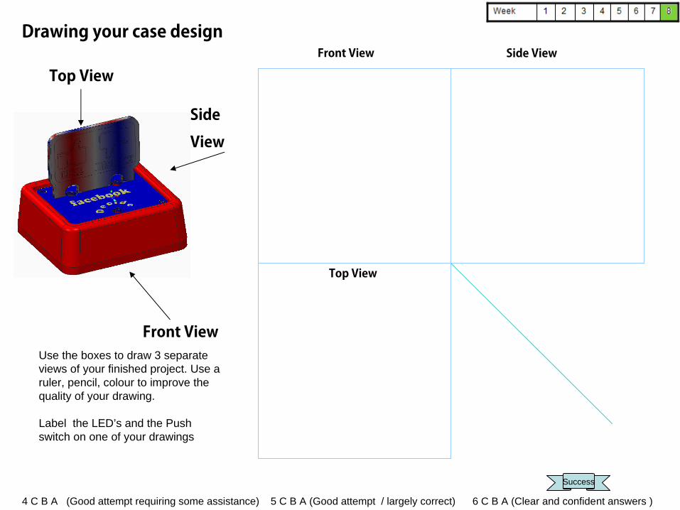
Front View Side View
Top View
Front View
Top View
Side
View
Drawing your case design
Use the boxes to draw 3 separate views of your finished project. Use a ruler, pencil, colour to improve the quality of your drawing.
Label the LED’s and the Push switch on one of your drawings
4 C B A (Good attempt requiring some assistance) 5 C B A (Good attempt / largely correct) 6 C B A (Clear and confident answers )
Success

Mr Hodgson’s Ultimate 555 timer Word search
Can you find as many words associated with the 555 timer circuit in the grid?The winner will receive my special prize!!!!!
Extension Work

Mr Hodgson’s 555 Timer Crossword Extension Work

Mr Hodgson’s 555 Timer Hangman
Choose words from the 3 columns and play hangman in the box with your neighbouring pupil. First to 5 correct words wins!!!!!!!!!!!
Extension Work

Assessment of MakingHeads or Tails
Follow Me
Stage
Description of Task Soldered across?
Features of component Your Comment on soldering/ quality / what you understand
Target W
eek to com
plete
Actual Week
Com
pleted?
1 Drill 1mm(x32) and 2mm(x10) 1
2 PUSH TO MAKE SWITCH
PTM 1
3 Diode D1 Silver band is Cathode 2
4 Resistor 1K R1K Brown, Black, Red, Gold 2
5 Resistor 10K R10K Brown, Black, Orange, Gold 2
6 Capacitor 10uF C10uF Long (+VE) and short leg (-VE) 3
7 Switch SW1 SW1 Yellow multi core wire (30cm) 3
8 PTM Switch PTM Yellow multi core wire (15cm) 3
9 Capacitor 0.01uF (10nF)
C0.01uF Orange circular shape. Legs equal length. 104 written on
3
10 8 Pin Socket 555 Notch with number ‘8’to top 4
11 Resistor R180 R180 Brown, Grey, Brown, Gold 4
12 Resistor R180 R180 Brown, Grey, Brown, Gold 4
13 LED #1 LED1 Long leg = red, short leg = black 5
14 LED #2 LED2 Long leg = red, short leg = black 5
15 BATTERY CLIP PWR Stitched through strain holes 5
16 INSERT 555 CHIP Pin 1 has a dimple (top left) 6
17 TESTING Battery – press switch to flash 6
18 Assemble in case PVC Mould and acrylic case 7
Name_________________