n-channel 100-v (d-s) mosfet
TRANSCRIPT

N-Channel 100-V (D-S) MOSFET
FEATURES• TrenchFET® Power MOSFET
• 175 °C Junction Temperature
• Low Thermal Resistance Package• 100 % Rg Tested
APPLICATIONS• Isolated DC/DC Converters
PRODUCT SUMMARY V(BR)DSS (V) RDS(on) (Ω) ID (A)
100 0.100 at VGS = 10 V 20
N-Channel MOSFET
G
D
S
Notes: a. Package limited.b. Duty cycle ≤ 1 %.c. See SOA curve for voltage derating.d. When Mounted on 1" square PCB (FR-4 material).
ABSOLUTE MAXIMUM RATINGS TC = 25 °C, unless otherwise notedParameter Symbol Limit Unit
Drain-Source Voltage VDS 100V
Gate-Source Voltage VGS ± 20
Continuous Drain Current (TJ = 175 °C)TC = 25 °C
ID20
ATC = 125 °C 16
Pulsed Drain Current IDM 70
Avalanche CurrentL = 0.1 mH
IAS 20
Single Pulse Avalanche Energyb EAS 200 mJ
Maximum Power DissipationbTC = 25 °C
PD WTA = 25 °Cd 3.75
Operating Junction and Storage Temperature Range TJ, Tstg - 55 to 175 °C
THERMAL RESISTANCE RATINGSParameter Symbol Limit Unit
Junction-to-Ambient PCB Mount (TO-263)d RthJA 40°C/W
Junction-to-Case (Drain) RthJC 0.4
RoHSCOMPLIANT
105
D2PAK(TO-263)
GD
S
www.VBsemi.tw
E-mail:China@VBsemi TEL:86-755-83251052E-mail:China@VBsemi TEL:86-755-83251052
www.VBsemi.twIRF520NS
1
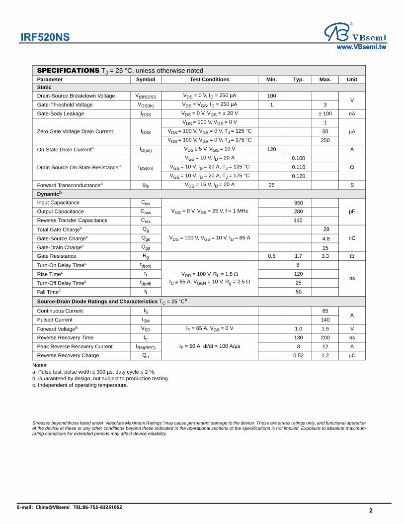
Notes:a. Pulse test; pulse width ≤ 300 µs, duty cycle ≤ 2 %.b. Guaranteed by design, not subject to production testing.c. Independent of operating temperature.
Stresses beyond those listed under “Absolute Maximum Ratings” may cause permanent damage to the device. These are stress ratings only, and functional operationof the device at these or any other conditions beyond those indicated in the operational sections of the specifications is not implied. Exposure to absolute maximumrating conditions for extended periods may affect device reliability.
SPECIFICATIONS TJ = 25 °C, unless otherwise notedParameter Symbol Test Conditions Min. Typ. Max. Unit
Static
Drain-Source Breakdown Voltage V(BR)DSS VDS = 0 V, ID = 250 µA 100V
Gate-Threshold Voltage VGS(th) VDS = VGS, ID = 250 µA 1 3
Gate-Body Leakage IGSS VDS = 0 V, VGS = ± 20 V ± 100 nA
Zero Gate Voltage Drain Current IDSS
VDS = 100 V, VGS = 0 V 1
µAVDS = 100 V, VGS = 0 V, TJ = 125 °C 50
VDS = 100 V, VGS = 0 V, TJ = 175 °C 250
On-State Drain Currenta ID(on) VDS ≥ 5 V, VGS = 10 V 120 A
Drain-Source On-State Resistancea rDS(on)
VGS = 10 V, ID = 20 A 0.100
ΩVGS = 10 V, ID = 20 A, TJ = 125 °C 0.110
VGS = 10 V, ID = 20 A, TJ = 175 °C 0.120
Forward Transconductancea gfs VDS = 15 V, ID = 20 A 25 S
Dynamicb
Input Capacitance Ciss
VGS = 0 V, VDS = 25 V, f = 1 MHz
950
pFOutput Capacitance Coss 280
Reverse Transfer Capacitance Crss 110
Total Gate Chargec Qg
VDS = 100 V, VGS = 10 V, ID = 65 A
28
nCGate-Source Chargec Qgs
Gate-Drain Chargec Qgd
Gate Resistance Rg 0.5 1.7 3.3 Ω
Turn-On Delay Timec td(on)
VDD = 100 V, RL = 1.5 Ω ID ≅ 65 A, VGEN = 10 V, Rg = 2.5 Ω
8
nsRise Timec tr 120
Turn-Off Delay Timec td(off) 25
Fall Timec tf 50
Source-Drain Diode Ratings and Characteristics TC = 25 °Cb
Continuous Current IS 65A
Pulsed Current ISM 140
Forward Voltagea VSD IF = 65 A, VGS = 0 V 1.0 1.5 V
Reverse Recovery Time trrIF = 50 A, di/dt = 100 A/µs
130 200 ns
Peak Reverse Recovery Current IRM(REC) 8 12 A
Reverse Recovery Charge Qrr 0.52 1.2 µC
4.8
15
www.VBsemi.tw
E-mail:China@VBsemi TEL:86-755-83251052E-mail:China@VBsemi TEL:86-755-83251052
www.VBsemi.twIRF520NS
2

TYPICAL CHARACTERISTICS 25 °C, unless otherwise noted
Output Characteristics
Transconductance
Capacitance
0
10
20
30
40
50
60
70
0 2 4 6 8 10
VDS - Drain-to-Source Voltage (V)
VGS = 10 thru6 V
2 V
- D
rain
Cur
rent
(A
)I D
5V
3V
0
30
60
90
120
150
180
0 20 40 60 80 100 120
- T
rans
cond
ucta
nce
(S)
gfs
TC = - 55 °C
25 °C
125 °C
ID - Drain Current (A)
0
200
400
600
800
1000
1200
1400
0 20
VDS - Drain-to-Source Voltage (V)
C -
Cap
acita
nce
(pF
)
Ciss
CossCrss
Transfer Characteristics
On-Resistance vs. Drain Current
Gate Charge
0
20
40
60
80
100
120
140
0 1 2 3 4 5 6 7
VGS - Gate-to-Source Voltage (V)
- D
rain
Cur
rent
(A
)I D
25 °C
- 55 °C
TC = 125 °C
0.000
0.010
0.020
0.030
0.040
0 20 40 60 80 100 120
ID - Drain Current (A)
VGS = 10 V
- O
n-R
esis
tanc
e (Ω
)r D
S(o
n)
0
4
8
12
16
20
0 25 50 75 100 125 150
- G
ate-
to-S
ourc
e V
olta
ge (
V)
Qg - Total Gate Charge (nC)
VG
S
VDS = 100 VID = 65 A
40 60 80 100 120
www.VBsemi.tw
E-mail:China@VBsemi TEL:86-755-83251052E-mail:China@VBsemi TEL:86-755-83251052
www.VBsemi.twIRF520NS
3

TYPICAL CHARACTERISTICS 25 °C, unless otherwise noted
On-Resistance vs. Junction Temperature
Avalanche Current vs. Time
r DS
(on)
- O
n-R
esis
tanc
e
(Nor
mal
ized
)
0.0
0.5
1.0
1.5
2.0
2.5
3.0
- 50 - 25 0 25 50 75 100 125 150 175
TJ - Junction Temperature (°C)
VGS = 10 VID = 20 A
tin (s)
1000
10
0.00001 0.001 0.1 1
0.1
(A)
I Dav
0.01
IAV (A) at TA = 150 °C
100
1
0.0001
IAV (A) at TA = 25 °C
Source-Drain Diode Forward Voltage
Drain Source Breakdownvs. Junction Temperature
VSD - Source-to-Drain Voltage (V)
- S
ourc
e C
urre
nt (
A)
I S
100
10
1
0.3 0.6 0.9 1.2
TJ = 25 °CTJ = 150 °C
0
180
190
200
210
220
230
240
- 50 - 25 0 25 50 75 100 125 150 175
TJ - Junction Temperature (°C)
(V)
V (BR
)DS
S
ID = 1.0 mA
www.VBsemi.tw
E-mail:China@VBsemi TEL:86-755-83251052E-mail:China@VBsemi TEL:86-755-83251052
www.VBsemi.twIRF520NS
4

THERMAL RATINGS
Maximum Avalanche and Drain Currentvs. Case Temperature
0
15
30
45
60
75
0 25 50 75 100 125 150 175
TC - Ambient Temperature (°C)
- D
rain
Cur
rent
(A
)I D
Safe Operating Area
VDS - Drain-to-Source Voltage (V)* VGS minimum VGS at which rDS(on) is specified
1000
10
0.1 1 10 1000
0.1
100
TC = 25 °C Single Pulse
- D
rain
Cur
rent
(A
)I D
1 ms10 ms100 msDC
10 µs
100 µs
1
100
>
rDS(on)
Limited*
Normalized Thermal Transient Impedance, Junction-to-CaseSquare Wave Pulse Duration (s)
2
1
0.1
0.0110-4 10-3 10-2 10-1 1
Nor
mal
ized
Effe
ctiv
e T
rans
ient
The
rmal
Impe
danc
e 0.2
0.1
Duty Cycle = 0.5
Single Pulse
0.05
0.02
www.VBsemi.tw
E-mail:China@VBsemi TEL:86-755-83251052E-mail:China@VBsemi TEL:86-755-83251052
www.VBsemi.twIRF520NS
5
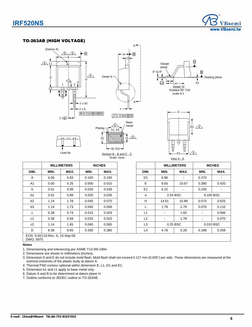
TO-263AB (HIGH VOLTAGE)
Notes1. Dimensioning and tolerancing per ASME Y14.5M-1994.2. Dimensions are shown in millimeters (inches).3. Dimension D and E do not include mold flash. Mold flash shall not exceed 0.127 mm (0.005") per side. These dimensions are measured at the
outmost extremes of the plastic body at datum A.4. Thermal PAD contour optional within dimension E, L1, D1 and E1.5. Dimension b1 and c1 apply to base metal only.6. Datum A and B to be determined at datum plane H.7. Outline conforms to JEDEC outline to TO-263AB.
5
4
1 3
L1
L2
D
B B
E
H
BA
Detail A
A
A
c
c2
A
2 x e
2 x b2
2 x b
0.010 A BM M± 0.004 BM
Basemetal
Plating b1, b3
(b, b2)
c1(c)
Section B - B and C - CScale: none
Lead tip
4
3 4
(Datum A)
2C C
B B
5
5
View A - A
E1
D1
E
4
4
B
H
Seating plane
Gaugeplane
0° to 8°
Detail “A”Rotated 90° CW scale 8:1
L3 A1L4L
MILLIMETERS INCHES MILLIMETERS INCHES
DIM. MIN. MAX. MIN. MAX. DIM. MIN. MAX. MIN. MAX.
A 4.06 4.83 0.160 0.190 D1 6.86 - 0.270 -
A1 0.00 0.25 0.000 0.010 E 9.65 10.67 0.380 0.420
b 0.51 0.99 0.020 0.039 E1 6.22 - 0.245 -
b1 0.51 0.89 0.020 0.035 e 2.54 BSC 0.100 BSC
b2 1.14 1.78 0.045 0.070 H 14.61 15.88 0.575 0.625
b3 1.14 1.73 0.045 0.068 L 1.78 2.79 0.070 0.110
c 0.38 0.74 0.015 0.029 L1 - 1.65 - 0.066
c1 0.38 0.58 0.015 0.023 L2 - 1.78 - 0.070
c2 1.14 1.65 0.045 0.065 L3 0.25 BSC 0.010 BSC
D 8.38 9.65 0.330 0.380 L4 4.78 5.28 0.188 0.208
ECN: S-82110-Rev. A, 15-Sep-08DWG: 5970
www.VBsemi.tw
E-mail:China@VBsemi TEL:86-755-83251052E-mail:China@VBsemi TEL:86-755-83251052
www.VBsemi.twIRF520NS
6

www.VBsemi.tw
E-mail:China@VBsemi TEL:86-755-83251052
RECOMMENDED MINIMUM PADS FOR D2PAK: 3-Lead
0.63
5
(16.
129)
Recommended Minimum PadsDimensions in Inches/(mm)
0.420
(10.668)
0.35
5
(9.0
17)
0.145(3.683)
0.135(3.429)
0.200
(5.080)
0.050
(1.257)
E-mail:China@VBsemi TEL:86-755-83251052
www.VBsemi.twIRF520NS
7
DisclaimerAll products due to improve reliability, function or design or for other reasons, product specifications and
data are subject to change without notice.
Taiwan VBsemi Electronics Co., Ltd., branches, agents, employees, and all persons acting on its or their representatives (collectively, the "Taiwan VBsemi"), assumes no responsibility for any errors, inaccuracies or incomplete data contained in the table or any other any disclosure of any information related to the product.(www.VBsemi.tw)
Taiwan VBsemi makes no guarantee, representation or warranty on the product for any particular purpose of any goods or continuous production. To the maximum extent permitted by applicable law on Taiwan VBsemi relinquished: (1) any application and all liability arising out of or use of any products; (2) any and all liability, including but not limited to special, consequential damages or incidental ; (3) any and all implied warranties, including a particular purpose, non-infringement and merchantability guarantee.
Statement on certain types of applications are based on knowledge of the product is often used in a typical application of the general product VBsemi Taiwan demand that the Taiwan VBsemi of. Statement on whether the product is suitable for a particular application is non-binding. It is the customer's responsibility to verify specific product features in the products described in the specification is appropriate for use in a particular application. Parameter data sheets and technical specifications can be provided may vary depending on the application and performance over time. All operating parameters, including typical parameters must be made by customer's technical experts validated for each customer application. Product specifications do not expand or modify Taiwan VBsemi purchasing terms and conditions, including but not limited to warranty herein.
Unless expressly stated in writing, Taiwan VBsemi products are not intended for use in medical, life saving, or life sustaining applications or any other application. Wherein VBsemi product failure could lead to personal injury or death, use or sale of products used in Taiwan VBsemi such applications using client did not express their own risk. Contact your authorized Taiwan VBsemi people who are related to product design applications and other terms and conditions in writing.
The information provided in this document and the company's products without a license, express or implied, by estoppel or otherwise, to any intellectual property rights granted to the VBsemi act or document. Product names and trademarks referred to herein are trademarks of their respective representatives will be all.
Material Category PolicyTaiwan VBsemi Electronics Co., Ltd., hereby certify that all of the products are determined to be
RoHS compliant and meets the definition of restrictions under Directive of the European Parliament 2011/65 / EU, 2011 Nian. 6. 8 Ri Yue restrict the use of certain hazardous substances in electrical and electronic equipment (EEE) - modification, unless otherwise specified as inconsistent.(www.VBsemi.tw)
Please note that some documents may still refer to Taiwan VBsemi RoHS Directive 2002/95 / EC. We confirm that all products identified as consistent with the Directive 2002/95 / EC European Directive 2011/65 /.
Taiwan VBsemi Electronics Co., Ltd. hereby certify that all of its products comply identified as halogen-free halogen-free standards required by the JEDEC JS709A. Please note that some Taiwanese VBsemi documents still refer to the definition of IEC 61249-2-21, and we are sure that all products conform to confirm compliance with IEC 61249-2-21 standard level JS709A.
www.VBsemi.tw
E-mail:China@VBsemi TEL:86-755-83251052E-mail:China@VBsemi TEL:86-755-83251052
www.VBsemi.twIRF520NS
8