mxic mx10f201fc data sheet - keil pointers are r0 and r1 of the selected register bank. - ram 128 to...
TRANSCRIPT

1
P/N:PM0730 REV. 0.1, FEB. 14, 2003
MX10F201FC
FEATURES OF MX10F201FC (80C51 with MTP memory and LCD)
- 80C51 CPU core
- 4.5 ~ 5.5V voltage range
- 2 to 16MHz clock frequency
- 16K bytes MTP memory for code memory
- 512 bytes internal data RAM
- Low power consumption
- Up to 16 digits LCD driver/controller
- Four 8 bit general purpose I/O ports
- Two standard 16-bit Timers
- On-chip Watch Dog Timer
- Two channel PWM outputs
- UART
- 8 interrupt sources
- 100 pin PQFP package
- Single clock or dual clock
- EMI compatibility
Features list
- 80C51 CPU core
- 4.5 ~ 5.5V operation voltage range
- 2 to 16MHz clock frequency
- 16K bytes MTP memory for code memory
- More than 100 times program/erase cycles
- More than 10 years data retention
- 512 bytes internal data RAM
- Low operation current
- Power saving modes
- User friendly power control for active mode current
- Idle mode
- Sleep mode
- Power down mode, can be wake up by external interrupts or RESET
- LCD driver/controller
- Max. 16-digits display at 1/4 duty LCD
- 1:1(static), 1:2, 1:3 or 1:4 selectable LCD multiplexing rate
- 4 backplane driver, 32 segment driver
- LCD directly drive capability with display memory
- VLCD to control LCD driving voltage, (VLCD-VSS)
- 4x8 general purpose I/O ports
- Provide software I2C capability
- Two standard 16-bit Timers (Timer 0,1)
- On-chip Watch Dog Timer (WDT)
- Two channel PWM outputs
- UART
- Up to 8 interrupt sources and 8 interrupt vectors
- 4 external sources
- 4 internal sources(Timer0,Timer1,watch Timer and UART)
- 100 pin PQFP package
- Single clock or dual clock
- single clock mode : 2~16MHz system clock for CPU,Timer0/1,WDT,UART and LCD
- dual clock mode : 2~16MHz system clock for CPU,Timer0/1,WDT,UART; while 32.768KHz sub-system
clock for LCD and watch timer.
- system clock is either crystal or RC activated
- EMC(Electro-Magnetic Compatibility) improved
2
P/N:PM0730 REV. 0.1, FEB. 14, 2003
MX10F201FC
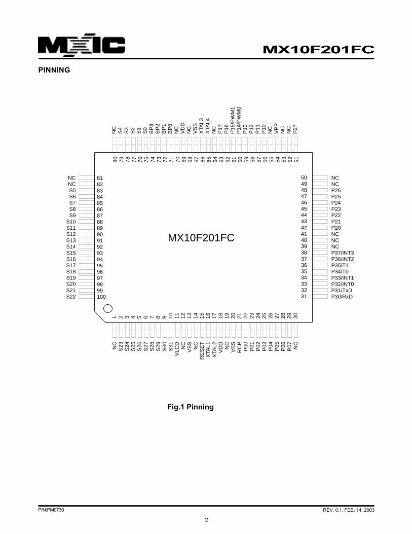
PINNING
NCNCP26P25P24P23P22P21P20NCNCNCP37/INT3P36/INT2P35/T1P34/T0P33/INT1P32/INT0P31/TxDP30/RxD
NCNCS5S6S7S8S9
S10S11S12S13S14S15S16S17S18S19S20S21S22
NC
S23
S24
S25
S26
S27
S28
S29
S30
S31
VLC
DN
CV
SS
NC
RE
SE
TX
TAL1
XTA
L2V
DD
NC
VS
SR
CP
P00
P01
P02
P03
P04
P05
P06
P07 NC
NC
S4
S3
S2
S1
S0
BP
3B
P2
BP
1B
P0
NC
VD
DN
CV
SS
XTA
L3X
TAL4
NC
P17
P16
P15
/PW
M1
P14
/PW
M0
P13
P12
P11
P10
NC
VP
PN
CN
CP
27
1 2 3 4 5 6 7 8 9 10 11 12 13 14 15 16 17 18 19 20 21 22 23 24 25 26 27 28 29 30
5049484746454443424140393837363534333231
80 79 78 77 76 75 74 73 72 71 70 69 68 67 66 65 64 63 62 61 60 59 58 57 56 55 54 53 52 51
81828384858687888990919293949596979899100
MX10F201FC
Fig.1 Pinning
3
P/N:PM0730 REV. 0.1, FEB. 14, 2003
MX10F201FC
Table. 1 Pin Description
I/O SYMBOL PIN \QFP 100 DESCRIPTION
O BP0-BP3 71~74 Backplane drive output line 0 to 3.
O S00-S31 75-79,83-100, Segment drive output line 0 to 31.
2-10
I/O P00-P07 22-29 Port:8-bit open drain bidirectional I/O Port
I/O P20-P27 42-48,51 Port: 8-bit quasi-bidirectional I/O Port with
internal pull-up
I/O P10-P17 56-63 Quasi-bidirectional I/O lines
P14 also for PWM channel 0
P15 also for PWM channel 1
I/O P30-P37 31-38 Quasi-bidirectional I/O lines
P30 31 also for UART Receive
P31 32 also for UART Transmit
P32-P33, also for external interrupt 0-3
P36-P37
P34 also for Timer0 external input
P35 also for Timer1 external input
I RESET 15 reset input
I VDD 18,69 Positive power supply
I VSS 13,20,67 Ground
I XTAL1 16 XTAL connection input
O XTAL2 17 XTAL connection output
I XTAL3 66 32.768KHz, XTAL input
O XTAL4 65 32.768KHz, XTAL output
I RCP 21 RC oscillator resistor connection input
I TEST/VPP 54 Supply 12V power for programming / erasing
I VLCD 11 LCD driver power supply
Note:
1. To avoid a 'Latch-up' effect at power-on , the voltage on any pin (at any time )must not be higher than VDD
+0.5 V
or lower Vss-0.5V respectively
2. The generation or use of a Port 3 pin as an alternative function is carried out automatically by the associated
Special Function Register (SFR) bit is properly written .
4
P/N:PM0730 REV. 0.1, FEB. 14, 2003
MX10F201FC
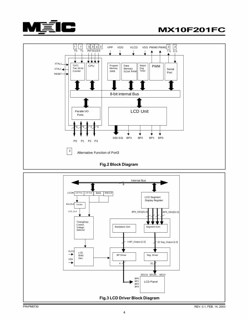
Fig.3 LCD Driver Block Diagram
Fig.2 Block Diagram
T0 T1 INT0/1/2/3
3 3
XTAL1
XTAL2
RESET
T0/T1Two 16-bitCounter
CPU ProgramMemory16KB
DataMemory512x8 RAM
PWMSerialPort
8-bit internal Bus
Parallel I/O Ports
LCD Unit
T D R D
S00-S31 BP3 BP2 BP1 BP0
8888
WatchDogTimer
P0 P1 P2 P3
Alternative Function of Port33
3 3 VPP VDD VLCD VSS PWM0 PWM13 3 33
LCD Segment Display Register
LCD Freq LCD Duty BIAS ENLCD
Div ider
Timing/DutyControl,VoltageSelector
LCD BIAS Gen.
Backplane Gen. Segment Gen.
BP Driver Seg. Driver
LCD Panel
SEG31 SEG30….SEG0
BP0BP1BP2BP3
LCON
Ext.CLK
LCD_CLK
8Internal Bus
BP3_SEG[31:0]BP0_SEG[31:0]
4 BP_Output [1:0] 32 Seg_Output [1:0]
324
VLCD
VSS

5
P/N:PM0730 REV. 0.1, FEB. 14, 2003
MX10F201FC
FUNCTIONAL DESCTIPTION
General
The MX10F201FC is a stand-alone high-performance and low power microcontroller designed for use in many
applications which need code programmability.
The Flash EPROM offers customers to program the device themselves. This feature increases the flexibility in
many applications, not only in development stage, but also in mass production stage.
In addition to the 80C51 standard functions, the MX10F201FC provides a number of dedicated hardware functions.
MX10F201FC is a control-oriented CPU with on-chip program and data memory. It can execute program with internal
memory up to 16k bytes. MX10F201FC has four software selectable modes of reduced activity for power reduction :
active power control, idle, sleep, and Power-down. The idle mode freezes the CPU while allowing the RAM, Timers,
serial ports, interrupt system and other peripherals to continue functioning. The Power-down mode saves the RAM
contents but freezes the oscillator causing all other chip functions to be inoperative. Power-down mode can be
terminated by an external reset ,and in addition , by either of the four external interrupts. The sleep mode behaves like
power down mode, but with LCD and oscillator still turning on. And sleep mode can be terminated as the power down
mode does.
Instruction Set Execution
The MX10F201FC uses the powerful instruction set of the 80C51. Additional SFRs are incorporated to control the
on-chip peripherals. The instruction set consists of 49 single-byte, 46 two-bytes, and 16 three-bytes instructions.
When using a 16MHz oscillator, 64 instructions execute in 750 ns and 45 instructions execute in 1.5 us. Multiply and
divide instructions execute in 3 us.
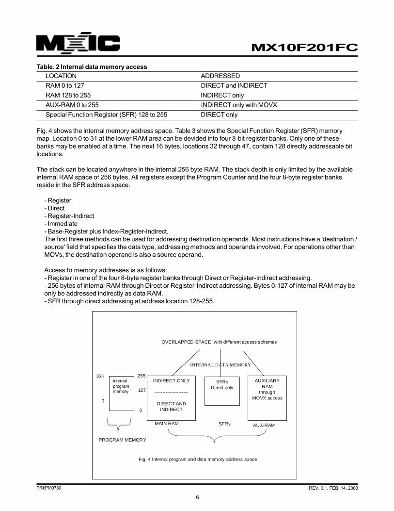
MEMORY ORGANIZATION
The Central Processing Unit (CPU) manipulates operands in three memory spaces; these are the 256 bytes
internal data memory (RAM), 256 byte auxiliary data memory (AUX-RAM) and 16k byte internal MTP program memory
(FEPROM).
Program Memory
The program memory address space of the MX10F201FC comprises an internal and an external memory space.
The MX10F201FC has 16k byte of program memory on-chip.
Program Protection
If the user choose to set security lock in MTP memory, the program content is protected from reading out of chip.
Internal Data Memory
The internal data memory is divided into three physically separated parts: 256 byte of RAM, 256 bytes of AUX-
RAM, and 128 bytes special function register area (SFR). These parts can be addressed as follows (see Fig.4 and
Table. 2)
- RAM 0 to 127 can be addressed directly and indirectly as in the 80C51. Address pointers are R0 and R1 of
the selected register bank.
- RAM 128 to 255 can only be addressed indirectly . Address pointers are R0 and R1 of the selected register
bank.
- AUX-RAM 0 to 255 is indirectly addressable as the external data memory locations 0 to 255 with the MOVX
instructions. Address pointers are R0 and R1 of the selected register bank and DPTR. When executing from
internal program memory, an access to AUX_RAM 0 to 255 will not affect the ports P0,P2,P3.6 and P3.7.
SFRs can only be addressed directly in the address range from 128 to 255.
6
P/N:PM0730 REV. 0.1, FEB. 14, 2003
MX10F201FC
Table. 2 Internal data memory access
LOCATION ADDRESSED
RAM 0 to 127 DIRECT and INDIRECT
RAM 128 to 255 INDIRECT only
AUX-RAM 0 to 255 INDIRECT only with MOVX
Special Function Register (SFR) 128 to 255 DIRECT only
Fig. 4 shows the internal memory address space. Table 3 shows the Special Function Register (SFR) memory
map. Location 0 to 31 at the lower RAM area can be devided into four 8-bit register banks. Only one of these
banks may be enabled at a time. The next 16 bytes, locations 32 through 47, contain 128 directly addressable bit
locations.
The stack can be located anywhere in the internal 256 byte RAM. The stack depth is only limited by the available
internal RAM space of 256 bytes. All registers except the Program Counter and the four 8-byte register banks
reside in the SFR address space.
- Register
- Direct
- Register-Indirect
- Immediate
- Base-Register plus Index-Register-Indirect.
The first three methods can be used for addressing destination operands. Most instructions have a 'destination /
source' field that specifies the data type, addressing methods and operands involved. For operations other than
MOVs, the destination operand is also a source operand.
Access to memory addresses is as follows:
- Register in one of the four 8-byte register banks through Direct or Register-Indirect addressing.
- 256 bytes of internal RAM through Direct or Register-Indirect addressing. Bytes 0-127 of internal RAM may be
only be addressed indirectly as data RAM.
- SFR through direct addressing at address location 128-255.
internalprogrammemory
16K
0
PROGRAM MEMORY
INDIRECT ONLY
---------------------
DIRECT ANDINDIRECT
MAIN RAM
255
127
0
SFRsDirect only
SFRs
AUXILIARYRAM
throughMOVX access
AUX-RAM
OVERLAPPED SPACE with different access schemes
Fig. 4 Internal program and data memory address space
INTERNAL DATA MEMORY
7
P/N:PM0730 REV. 0.1, FEB. 14, 2003
MX10F201FC
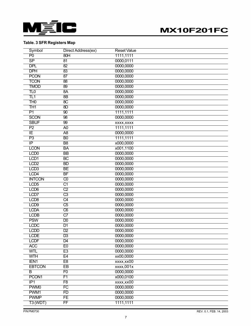
Symbol Direct Address(ex) Reset Value
P0 80H 1111,1111
SP 81 0000,0111
DPL 82 0000,0000
DPH 83 0000,0000
PCON 87 0000,0000
TCON 88 0000,0000
TMOD 89 0000,0000
TL0 8A 0000,0000
TL1 8B 0000,0000
TH0 8C 0000,0000
TH1 8D 0000,0000
P1 90 1111,1111
SCON 98 0000,0000
SBUF 99 xxxx,xxxx
P2 A0 1111,1111
IE A8 0000,0000
P3 B0 1111,1111
IP B8 x000,0000
LCON BA x001,1100
LCD0 BB 0000,0000
LCD1 BC 0000,0000
LCD2 BD 0000,0000
LCD3 BE 0000,0000
LCD4 BF 0000,0000
INTCON C0 0000,0000
LCD5 C1 0000,0000
LCD6 C2 0000,0000
LCD7 C3 0000,0000
LCD8 C4 0000,0000
LCD9 C5 0000,0000
LCDA C6 0000,0000
LCDB C7 0000,0000
PSW D0 0000,0000
LCDC D1 0000,0000
LCDD D2 0000,0000
LCDE D3 0000,0000
LCDF D4 0000,0000
ACC E0 0000,0000
WTL E3 0000,0000
WTH E4 xx00,0000
IEN1 E8 xxxx,xx00
EBTCON EB xxxx,001x
B F0 0000,0000
PCON1 F1 x000,0100
IP1 F8 xxxx,xx00
PWM0 FC 0000,0000
PWM1 FD 0000,0000
PWMP FE 0000,0000
T3 (WDT) FF 1111,1111
Table. 3 SFR Registers Map
8
P/N:PM0730 REV. 0.1, FEB. 14, 2003
MX10F201FC
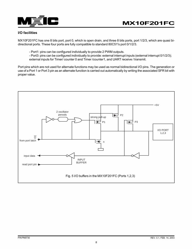
I/O facilities
MX10F201FC has one 8 bits port, port 0, which is open drain, and three 8 bits ports, port 1/2/3, which are quasi bi-
directional ports. These four ports are fully compatible to standard 80C51's port 0/1/2/3.
- Port1: pins can be configured individually to provide 2 PWM outputs.
- Port3: pins can be configured individually to provide: external interrupt inputs (external interrupt 0/1/2/3);
external inputs for Timer/ counter 0 and Timer /counter1, and UART receive / transmit.
Port pins which are not used for alternate functions may be used as normal bidirectional I/O pins. The generation or
use of a Port 1 or Port 3 pin as an alternate function is carried out automatically by writing the associated SFR bit with
proper value.
Fig. 5 I/O buffers in the MX10F201FC (Ports 1,2,3)
2 oscillatorpenods
strong pull-up
P1
n
P2
INPUTBUFFER
from port latch
input data
read port pin
O
P3
+5V
I/O PORT1,2,3
9
P/N:PM0730 REV. 0.1, FEB. 14, 2003
MX10F201FC
Timer/Counter
MX10F201FC's Timer/Counter 0 and 1 are fully compatible to standard 80C51's.
The MX10F201FC's contains two 16-bit Timer/counters, Timer 0 and Timer 1. Timer 0 and Timer 1 may be
programmed to carry out the following functions:
- measure time intervals and pulse durations
- count events
- generate interrupt requests.
Timer 0 and Timer 1
Timers 0 and 1 each have a control bit in TMOD SFR that selects the Timer or counter function of the
corresponding Timer. In the Timer function, the register is incremented every machine cycle. Thus, one can think of
it as counting machine cycles. Since a machine cycle consists of 12 oscillator periods, the count rate is 1/12 of
the oscillator frequency.
In the counter function, the register is incremented in response to a HIGH-to-LOW transition at the corresponding
samples, when the transition shows a HIGH in one cycle and a LOW in the next cycle, the counter is incremented.
Thus, it takes two machine cycles (24 oscillator periods) to recognize a HIGH-to-LOW transition. There are no
restrictions on the duty cycle of the external input signal, but to ensure that a given level is sampled at least once
before it changes, it should be held for at least one full machine cycle.
Timer 0 and Timer 1 can be programmed independently to operate in one of four modes (refer to table 5) :
- Mode 0 : 8-bit Timer/counter with devided-by-32 prescaler
- Mode 1 : 16-bit Timer/counter
- Mode 2 : 8-bit Timer/counter with automatic reload
- Mode 3 : Timer 0 :one 8-bit Timer/counter and one 8-bits Timer. Timer 1 :stopped.
When Timer 0 is in Mode 3, Timer 1 can be programmed to operate in Modes 0, 1 or 2 but cannot set an interrupt
request flag and generate an interrupt. However, the overflow from Timer 1 can be used to pulse the Serial Port
transmission-rgate generator. With a 16 MHz crystal, the counting frequency of these Timer/counters is as follows:
- in the Timer function, the Timer is incremented at a frequency of 1.33 MHz (oscillator frequency divided by 12).
- in the counter function, the frequency handling range for external inputs is 0 Hz to 0.66 MHz (oscillator
frequency divided by 24).
Both internal and external inputs can be gated to the Timer by a second external source for directly measuring
pulse duration.
The Timers are started and stopped under software control. Each one sets its interrupt request flag when it
overflows from all logic 1's to all logic 0's (respectively, the automatic reload value), with the exception of Mode 3
as previously described.
TMOD : TIMER/COUNTER MODE CONTROL REGISTER
This register is located at address 89H.
Table. 4 TMOD SFR (89H)
7 6 5 4 3 2 1 0
GATE C/ T M1 M0 GATE C/ T M1 M0
(MSB) (LSB)
TIMER 1 TIMER 0
keep the above table with the following table
10
P/N:PM0730 REV. 0.1, FEB. 14, 2003
MX10F201FC
Table. 5 Description of TMOD bits
MNEMONIC POSITION FUNCTION
TIMER 1
GATE TMOD.7 Timer 1 gating control : when set, Timer/counter '1' is enabled only while 'Int1'
pin is high and 'tr1' control bit is set. when cleared, Timer/counter '1' is enabled
whenever 'tr1' control bit is set.
C/T TMOD.6 Timer or counter selector: cleared for Timer operation (input from internal
system clock). set for counter operation (input from 'T1' input pin).
M1 TMOD.5 Operation mode: see table 6.
M0 TMOD.4 Operation mode: see table 6.
TIMER 0
GATE TMOD.3 Timer 0 gating control: when set, Timer/Counter '0' is enabled only while 'Int0'
pin is high and 'tr0' control bit is set. when cleared, Timer/counter '0' is enabled
whenever 'tr0' control bit is set.
C/T TMOD.2 Timer or counter selector: cleared for Timer operation (input from internal
system clock). set for counter operation (input from 'T0' input pin).
M1 TMOD.1 Operation mode: see table 6.
M0 TMOD.0 Operation mode: see table 6.
Table. 6 TMOD M1 and M0 operating modes
M1 M0 FUNCTION
0 0 8-bit Timer/counter : 'THx' with 5-bit prescaler.
0 1 16-bit Timer/counter : 'THx' and 'TLx' are cascaded, there is no prescaler.
1 0 8-bit autoload Timer/counter : 'THx' holds a value which is to be reloaded into 'TLx' each time it
overflows.
1 1 Timer 0: TL0 is an 8-bit Timer/counter controlled by the standard Timer 0 control bits. TH0 is an 8-
bit Timer controlled by Timer 1 control bits.
1 1 Timer 1 : Timer/counter 1 stopped.
TCON : TIMER/COUNTER CONTROL REGISTER
This register is located at address 88H.
Table. 7 TCON SFR (88H)
7 6 5 4 3 2 1 0
TF1 TR1 TF0 TR0 IE1 IT1 IE0 IT0
(MSB) (LSB)
keep the above table with the following table

11
P/N:PM0730 REV. 0.1, FEB. 14, 2003
MX10F201FC
Table. 8 Description of TCON bits
MNEMONIC POSITION FUNCTION
TF1 TCON.7 Timer 1 overflow flag : set by hardware on Timer/Counter overflow. Cleared when
interrupt is processed.
TR1 TCON.6 Timer 0 overflow flag : set by hardware on Timer/Counter overflow. Cleared when
interrupt is processed.
TF0 TCON.5 Timer 0 overflow flag: set by hardware on Timer/Counter overflow. Cleared when
interrupt is processed.
TR0 TCON.4 Timer 0 control bit : set/cleared by software to turn Timer/counter ON/OFF.
IE1 TCON.3 Interrupt 1 edge flag: set by hardware when external interrupt is detected. Cleared
when interrupt is processed.
IT1 TCON.2 Interrupt 1 type control bit : set/cleared by software to specify falling edge/LOW
level triggered external interrupt.
IE0 TOCN.1 Interrupt 0 edge flag: set by hardware when external interrupt is detected. Cleared
when interrupt is processed.
IT0 TOCN.0 Interrupt 0 type control bit: set/cleared by software tospecify falling edge/LOW
level triggered external interrupt.

12
P/N:PM0730 REV. 0.1, FEB. 14, 2003
MX10F201FC
Interrupt system
The MX10F201FC contains a 8-source 4 external interrupts, Timer 0, Timer1, watch timer and UART structures
with two priority levels.
Each External interrupts INT0, INT1, INT2, and INT3 can be either level-activated or transition-activated depending
on bits IT0 and IT1 in TCON SFR and IT2, IT3 in INTCON SFR. The flags that actually generate these interrupts
are bits IE0, IE1 in TCON and IE2,IE3 in INTCON. When an external interrupt is generated, the corresponding
request flag is cleared by the hardware when the service routine is vectored to, if the interrupt is transition-
activated. If the interrupt is level-activated the external source has to hold the request active until the requested
interrupt is actually generated. Then it has to deactive the request before the interrupt service routine is completed,
otherwise another interrupt will be generated.
The Timer 0 and Timer 1 Interrupts are generated by TF0 and TF1, which are set by a rollover in their respective
Timer/counter register (except for Timer 0 in Mode 3 of the serial interface). When a Timer interrupt is generated,
the flag that generated it is cleared by the on-chip hardware when the service routine is vectored to.
IE : INTERRUPT ENABLE REGISTER
This register is located at address A8H.
Table. 9 IE SFR (A8H)
7 6 5 4 3 2 1 0
EA EX3 EX2 ES ET1 EX1 ET0 EX0
(MSB) (LSB)
keep the above table with the following table
Table. 10 Description of IE bits
MNEMONIC POSITION FUNCTION
EA IE.7 Disable all interrupt
- Low, all disabled.
- High, each interrupt source is individually enabled or disabled by setting or
clearing its enable bit.
EX3 IE.6 Enable / Disable External interrupt 3.
- Low, disabled
- High, enabled
EX2 IE.5 Enable / Disable External Interrupt 2.
- Low, disabled
- High, enabled
ES IE.4 Enable / Disable UART interrupt.
- Low, disabled
- High, enabled
ET1 IE.3 Enable / Disable Timer1 overflow interrupt.
EX1 IE.2 Enable / Disable External interrupt 1.
- Low, disabled
- High, enabled
ET0 IE.1 Enable / disable Timer0 overflow interrupt.
EX0 IE.0 Enable / Disable External interrupt 0.
- Low, disabled
- High, enabled

13
P/N:PM0730 REV. 0.1, FEB. 14, 2003
MX10F201FC
IP : INTERRUPT PRIORITY REGISTER
This register is located at address B8H.
Table. 12 IP SFR (B8H)
7 6 5 4 3 2 1 0
- PX3 PX2 PS PT1 PX1 PT0 PX0 (LSB)
keep the above table with the following table
Table. 13 Description of IP bits
MNEMONIC POSITION FUNCTION
- IP.7 RESERVED
PX3 IP.6 Define External interrupt 3 interrupt priority level.
- High, assign a high priority level.
PX2 IP.5 Define External interrupt 2 interrupt priority level.
- High, assign a high priority level.
PS1 IP.4 Define interrupt priority level of UART.
PT1 IP.3 Define Timer1 overflow interrupt priority level.
PX1 IP.2 Define External interrupt 1 interrupt priority level.
- High, assign a high priority level.
PT0 IP.1 Define Timer0 overflow interrupt priority level.
PX0 IP.0 Define External interrupt 0 interrupt priority level.
- High, assign a high priority level.
IP1 : INTERRUPT PRIORITY REGISTER 2
Table. 14 IP1 SFR (F8H)
7 6 5 4 3 2 1 0
- - - - - - PWT 0
PWT : Define Watch Timer interrupt priority level.
IEN1 : INTERRUPT ENABLE REGISTER 2
Table. 11 IEN1 SFR (E8H)
7 6 5 4 3 2 1 0
- - - - - - EWT 0
EWT : Enable / Disable Watch Timer interrupt.

14
P/N:PM0730 REV. 0.1, FEB. 14, 2003
MX10F201FC
Table. 15 INTCON SFR (C0H)
7 6 5 4 3 2 1 0
0 0 WTF WTR IE3 IT3 IE2 IT2
Table. 16 Description of INTCON bits
IE3/2 : External interrupt 3/2 edge flag. Set by H/W when exteranl interrupt is detected, and cleared when interrupt
is processed.
IT3/2 : External interrupt 3/2 type control bit. Set/cleared by S/W to specify falling edge/low level triggered external
interrupt.
WTF : Watch timer overflow interrupt flog. Set by H/W when watch timer overflow occurred, and cleared by S/W or
warm/cold reset.
WTR : Watch timer enable bit. Set/ cleared by S/W
Table. 17 INTERRUPT VECTORS & PRIORITY WITHIN LEVELS
source name Priority Within Level Vector Address
Ext. interrupt0 IE0 1(Highest) 0003H
Timer0 overflow TF0 2 000BH
Ext. interrupt1 IE1 3 0013H
Timer1 overflow TF1 4 001BH
UART interrupt IS 5 0023H
Ext. interrupt2 IE2 6 002BH
Ext. interrupt3 IE3 7 0033H
Watch timer overflow WTF 8 003BH
15
P/N:PM0730 REV. 0.1, FEB. 14, 2003
MX10F201FC
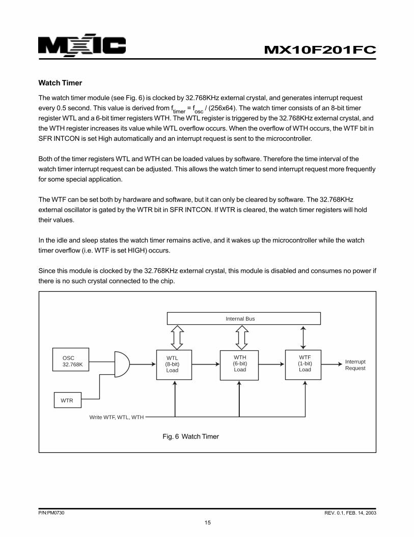
Watch Timer
The watch timer module (see Fig. 6) is clocked by 32.768KHz external crystal, and generates interrupt request
every 0.5 second. This value is derived from ftimer
= fosc
/ (256x64). The watch timer consists of an 8-bit timer
register WTL and a 6-bit timer registers WTH. The WTL register is triggered by the 32.768KHz external crystal, and
the WTH register increases its value while WTL overflow occurs. When the overflow of WTH occurs, the WTF bit in
SFR INTCON is set High automatically and an interrupt request is sent to the microcontroller.
Both of the timer registers WTL and WTH can be loaded values by software. Therefore the time interval of the
watch timer interrupt request can be adjusted. This allows the watch timer to send interrupt request more frequently
for some special application.
The WTF can be set both by hardware and software, but it can only be cleared by software. The 32.768KHz
external oscillator is gated by the WTR bit in SFR INTCON. If WTR is cleared, the watch timer registers will hold
their values.
In the idle and sleep states the watch timer remains active, and it wakes up the microcontroller while the watch
timer overflow (i.e. WTF is set HIGH) occurs.
Since this module is clocked by the 32.768KHz external crystal, this module is disabled and consumes no power if
there is no such crystal connected to the chip.
Fig. 6 Watch Timer
Internal Bus
Write WTF, WTL, WTH
InterruptRequest
WTR
OSC32.768K
WTH(6-bit)Load
WTF(1-bit)Load
WTL(8-bit)Load
16
P/N:PM0730 REV. 0.1, FEB. 14, 2003
MX10F201FC
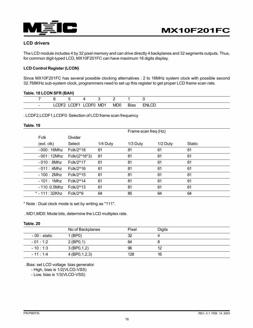
LCD drivers
The LCD module includes 4 by 32 pixel memory and can drive directly 4 backplanes and 32 segments outputs. Thus,
for common digit-typed LCD, MX10F201FC can have maximum 16 digits display.
LCD Control Register (LCON)
Since MX10F201FC has several possible clocking alternatives : 2 to 16MHz system clock with possible second
32.768KHz sub-system clock, programmers need to set up this register to get proper LCD frame scan rate.
Table. 18 LCON SFR (BAH)
7 6 5 4 3 2 1 0
- LCDF2 LCDF1 LCDF0 MD1 MD0 Bias ENLCD
. LCDF2,LCDF1,LCDF0: Selection of LCD frame scan frequency
Table. 19
Frame scan freq (Hz)
Fclk Divider
(ext. clk) Select 1/4 Duty 1/3 Duty 1/2 Duty Static
- 000 : 16Mhz Fclk/2^18 61 81 61 61
- 001 : 12Mhz Fclk/(2^16*3) 61 81 61 61
- 010 : 8Mhz Fclk/2^17 61 81 61 61
- 011 : 4Mhz Fclk/2^16 61 81 61 61
- 100 : 2Mhz Fclk/2^15 61 81 61 61
- 101 : 1Mhz Fclk/2^14 61 81 61 61
- 110 :0.5Mhz Fclk/2^13 61 81 61 61
* - 111 : 32Khz Fclk/2^9 64 85 64 64
* Note : Dual clock mode is set by writing as "111".
. MD1,MD0: Mode bits, determine the LCD multiplex rate.
Table. 20
No of Backplanes Pixel Digits
- 00 : static 1 (BP0) 32 4
- 01 : 1:2 2 (BP0,1) 64 8
- 10 : 1:3 3 (BP0,1,2) 96 12
- 11 : 1:4 4 (BP0,1,2,3) 128 16
. Bias: set LCD voltage bias generator.
- High, bias is 1/2(VLCD-VSS)
- Low, bias is 1/3(VLCD-VSS)

17
P/N:PM0730 REV. 0.1, FEB. 14, 2003
MX10F201FC
Table. 21
LCD Drive Mode No of BPs LCD Bias Voff(rms) Von(rms) Contrast
static 1 static 0 1 infinity
1:2 2 1/2 0.354 0.791 2.236
1:2 2 1/3 0.333 0.745 2.236
1:3 3 1/3 0.333 0.638 1.915
1:4 4 1/3 0.333 0.577 1.732
. ENLCD: Enable/Disable LCD
- Low, all segment and backplanes drivers are set to the Vss level.
- High, the LCD is enable and digits display is possible.
LCD segment display register : contain the on/off information of 4 by 32 segments of LCD
Table. 22
Register Address Bit7 Bit6 Bit5 Bit4 Bit3 Bit2 Bit1 Bit0
LCD0 BBH SEG1 SEG0
LCD1 BCH SEG3 SEG2
LCD2 BDH SEG5 SEG4
LCD3 BEH SEG7 SEG6
LCD4 BFH SEG9 SEG8
LCD5 C1H SEG11 SEG10
LCD6 C2H SEG13 SEG12
LCD7 C3H SEG15 SEG14
LCD8 C4H SEG17 SEG16
LCD9 C5H SEG19 SEG18
LCDA C6H SEG21 SEG20
LCDB C7H SEG23 SEG22
LCDC D1H SEG25 SEG24
LCDD D2H SEG27 SEG26
LCDE D3H SEG29 SEG28
LCDF D4H SEG31 SEG30
BP3 BP2 BP1 BP0 BP3 BP2 BP1 BP0
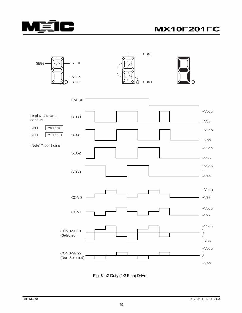
LCD drive mode waveform : used to control the voltage level of backplane and segment outputs
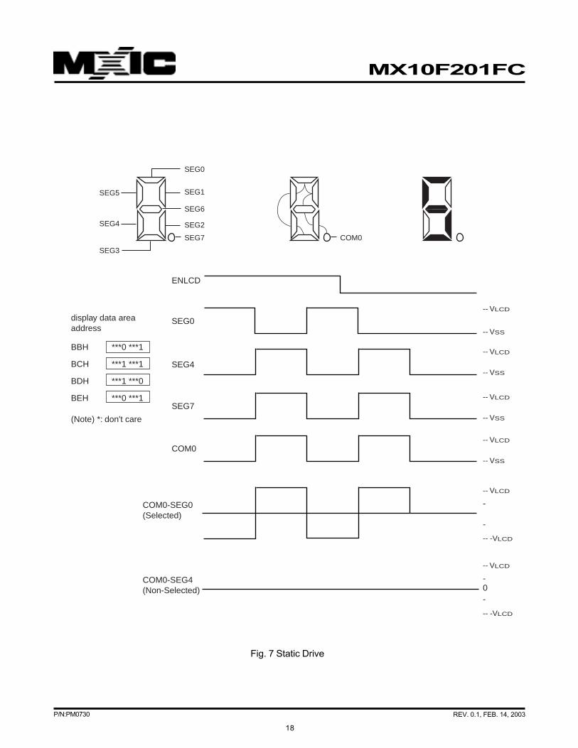
. Static drive mode
. 1:2 multiplex drive mode with 1/2 bias
. 1:2 multiplex drive mode with 1/3 bias
. 1:3 multiplex drive mode with 1/3 bias
. 1:4 multiplex drive mode with 1/3 bias
18
P/N:PM0730 REV. 0.1, FEB. 14, 2003
MX10F201FC
Fig. 7 Static Drive
ENLCD
SEG3
SEG4
-- VLCD
-- VLCD
-- VSS
-- VSS
-- VLCD
-- VSS
-- VLCD
-- VSS
SEG0
SEG4
display data areaaddress
(Note) *: don't care
BBH
BCH
BDH
BEH
***0 ***1
***1 ***1
***1 ***0
***0 ***1SEG7
COM0
-- VLCD
-
-
-- -VLCD
-- VLCD
-0-
-- -VLCD
COM0-SEG0(Selected)
COM0-SEG4(Non-Selected)
SEG5
SEG0
SEG1
SEG6
SEG2
SEG7 COM0
19
P/N:PM0730 REV. 0.1, FEB. 14, 2003
MX10F201FC
Fig. 8 1/2 Duty (1/2 Bias) Drive
ENLCD
-- VLCD
-- VSS
-- VLCD
-- VSS
-- VLCD
-- VSS
-- VLCD
-
-
-0
-- VSS
-- VLCD
-- VSS
-- VLCD
-- VSS
-- VLCD
-- VSS
-
-0
-- VLCD
-- VSS
SEG0
SEG1
display data areaaddress
(Note) *: don't care
BBH
BCH
**01 **01
**11 **10
SEG3
SEG2
COM0
COM1
COM0-SEG1(Selected)
COM0-SEG2(Non-Selected)
SEG3 SEG0
SEG2
SEG1 COM1
COM0
20
P/N:PM0730 REV. 0.1, FEB. 14, 2003
MX10F201FC
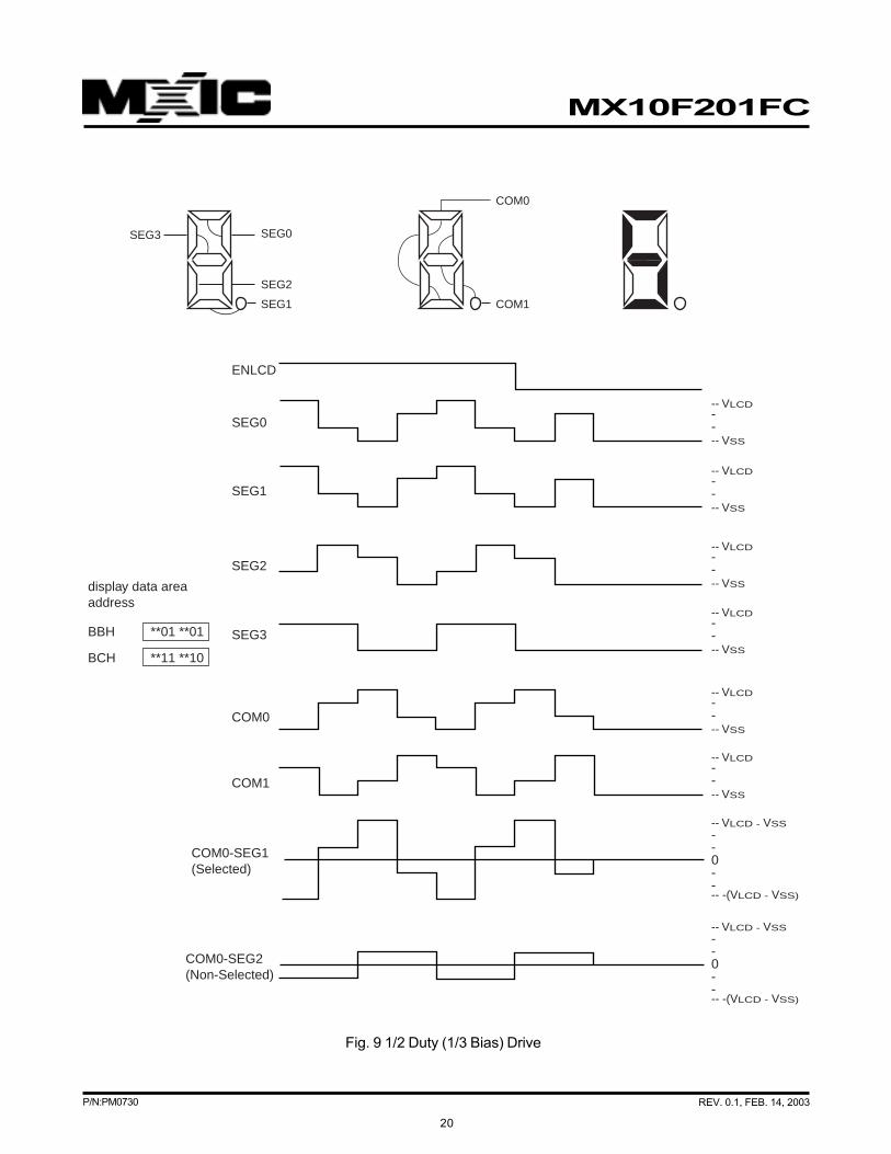
Fig. 9 1/2 Duty (1/3 Bias) Drive
ENLCD
-- VLCD
-- VSS
--
-- VLCD
-- VSS
--
-- VLCD
-- VSS
--
-- VLCD
-- VSS
--
-- VLCD
-- VSS
--
-- VLCD
-- VSS
--
--
--
0
-- VLCD - VSS
-- -(VLCD - VSS)
--
--
0
-- VLCD - VSS
-- -(VLCD - VSS)
SEG0
SEG1
display data areaaddress
BBH
BCH
**01 **01
**11 **10
SEG3
SEG2
COM0
COM1
COM0-SEG1(Selected)
COM0-SEG2(Non-Selected)
SEG3 SEG0
SEG2
SEG1 COM1
COM0
21
P/N:PM0730 REV. 0.1, FEB. 14, 2003
MX10F201FC
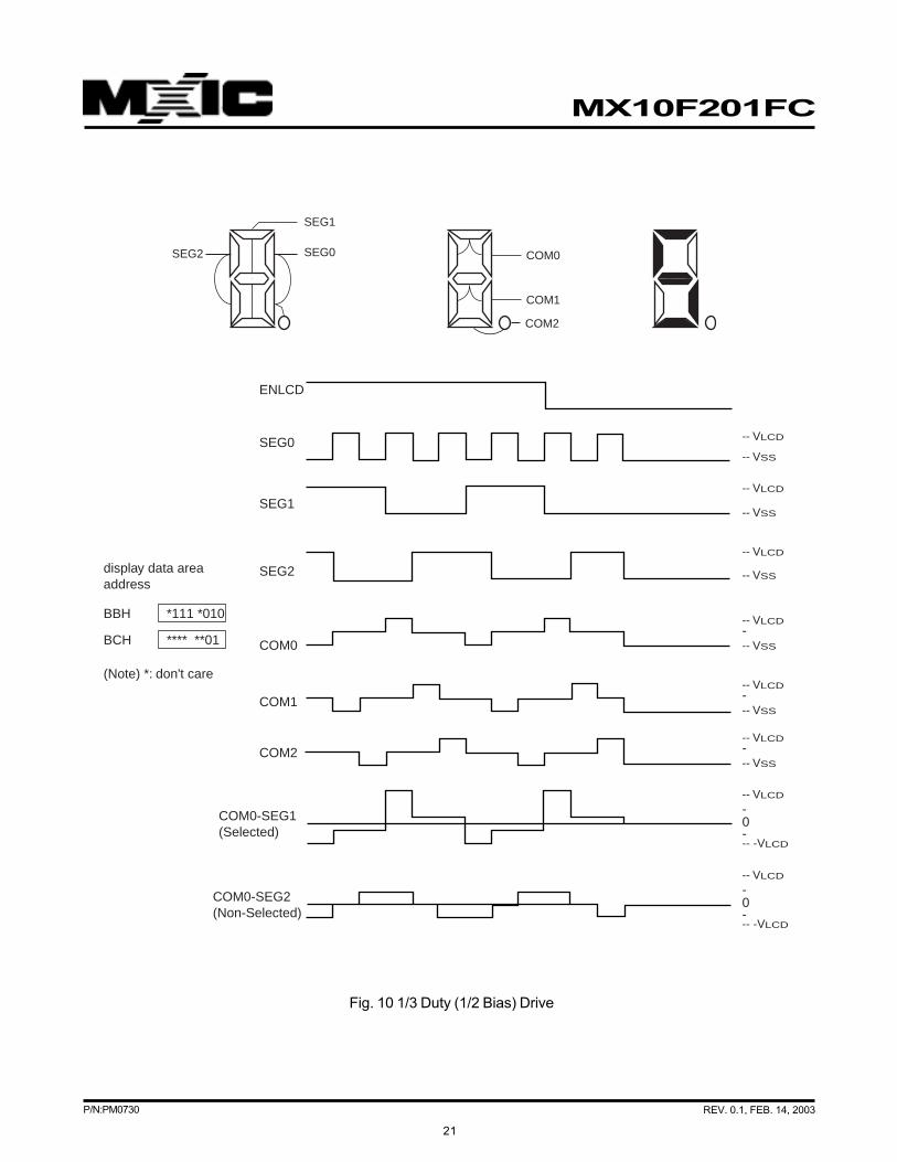
Fig. 10 1/3 Duty (1/2 Bias) Drive
ENLCD
-- VLCD
-- VSS
-- VLCD
-- VSS
-- VLCD
-- VSS
-- VLCD
-- VSS
-
-- VLCD
-- VSS
-
-- VLCD
-- VSS
-
-
-0
-- VLCD
-- -VLCD
-
-0
-- VLCD
-- -VLCD
SEG0
SEG1
display data areaaddress
(Note) *: don't care
BBH
BCH
*111 *010
**** **01
SEG2
COM0
COM1
COM2
COM0-SEG1(Selected)
COM0-SEG2(Non-Selected)
SEG2 SEG0
SEG1
COM2
COM0
COM1

22
P/N:PM0730 REV. 0.1, FEB. 14, 2003
MX10F201FC
Fig. 11 1/3 Duty (1/3 Bias) Drive
ENLCD
-- VLCD
-- VSS--
-- VLCD
-- VSS--
-- VLCD
-- VSS--
-- VLCD
-- VSS--
-- VLCD
-- VSS--
-- VLCD
-- VSS--
-
-0
-- VLCD
-- -VLCD
-
-0
-- VLCD
-- -VLCD
SEG0
SEG1display data areaaddress
(Note) *: don't care
BBH
BCH
*111 *010
**** **01SEG2
COM0
COM1
COM2
COM0-SEG1(Selected)
COM0-SEG2(Non-Selected)
SEG2 SEG0
SEG1
COM2
COM0
COM1

23
P/N:PM0730 REV. 0.1, FEB. 14, 2003
MX10F201FC
Fig .12 1/4 Duty (1/3 Bias) Drive
ENLCD
-- VLCD
-- VSS--
-- VLCD
-- VSS--
-- VLCD
-- VSS--
-- VLCD
-- VSS--
-- VLCD
-- VSS--
-- VLCD
-- VSS--
-
-0
-- VLCD
-- -VLCD
-
-0
-- VLCD
-- -VLCD
SEG0
SEG1
display data areaaddress
BBH 10110101
COM1
COM0
COM2
COM3
COM0-SEG0(Selected)
COM0-SEG1(Non-Selected)
SEG1
SEG0 COM3
COM1
COM0
COM2
24
P/N:PM0730 REV. 0.1, FEB. 14, 2003
MX10F201FC
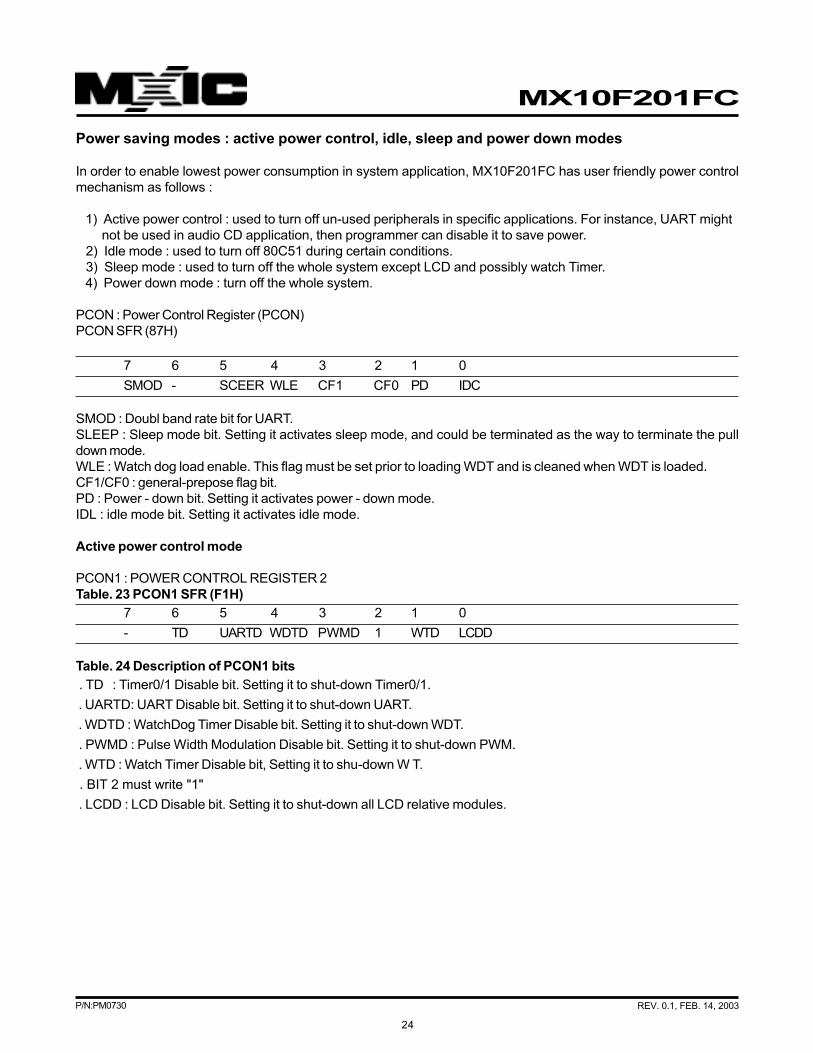
Power saving modes : active power control, idle, sleep and power down modes
In order to enable lowest power consumption in system application, MX10F201FC has user friendly power control
mechanism as follows :
1) Active power control : used to turn off un-used peripherals in specific applications. For instance, UART might
not be used in audio CD application, then programmer can disable it to save power.
2) Idle mode : used to turn off 80C51 during certain conditions.
3) Sleep mode : used to turn off the whole system except LCD and possibly watch Timer.
4) Power down mode : turn off the whole system.
PCON : Power Control Register (PCON)
PCON SFR (87H)
7 6 5 4 3 2 1 0
SMOD - SCEER WLE CF1 CF0 PD IDC
SMOD : Doubl band rate bit for UART.
SLEEP : Sleep mode bit. Setting it activates sleep mode, and could be terminated as the way to terminate the pull
down mode.
WLE : Watch dog load enable. This flag must be set prior to loading WDT and is cleaned when WDT is loaded.
CF1/CF0 : general-prepose flag bit.
PD : Power - down bit. Setting it activates power - down mode.
IDL : idle mode bit. Setting it activates idle mode.
Active power control mode
PCON1 : POWER CONTROL REGISTER 2
Table. 23 PCON1 SFR (F1H)
7 6 5 4 3 2 1 0
- TD UARTD WDTD PWMD 1 WTD LCDD
Table. 24 Description of PCON1 bits
. TD : Timer0/1 Disable bit. Setting it to shut-down Timer0/1.
. UARTD: UART Disable bit. Setting it to shut-down UART.
. WDTD : WatchDog Timer Disable bit. Setting it to shut-down WDT.
. PWMD : Pulse Width Modulation Disable bit. Setting it to shut-down PWM.
. WTD : Watch Timer Disable bit, Setting it to shu-down W T.
. BIT 2 must write "1"
. LCDD : LCD Disable bit. Setting it to shut-down all LCD relative modules.
25
P/N:PM0730 REV. 0.1, FEB. 14, 2003
MX10F201FC
RC oscillator function
MX10F201FC provides a RC oscillator function for the application that does not need very accurate system clock
frequency and has to save the cost of crystal oscillator. As shown in Fig. 13, to use the RC oscillator function as
the system clock source, a suggested 50K~200K can be connected between the RCP pin and ground. The XTAL1
pin has to be connected to ground or the internal clock system may be failed. When the system clock source
comes from the crystal oscillator, the RCP pin is suggested to connect to VDD. The following table shows
approximately the relationship between the RC oscillator clock frequency and the resistor value.
Resistor Value (K ohm) RC oscillator clock frequency (MHz)
5V 3V
50 12~14 9~11
75 10~12 7.5~9
100 9~10 6.5~8
125 8~9 6~7.5
150 ~7.5 5.5~6.5
175 ~6.5 5.2~5.8
200 ~6 4.7~5.3
XTAL1 XTAL1
XTAL2 XTAL2
RCP RCP
VDDResistor
(a) (b)
Fig. 13 System clock connection way : (a) Use RC oscillator as system
clock source, (b) Use crystal oscillator as system clock source.
Table. 25 RC oscillator reference table
26
P/N:PM0730 REV. 0.1, FEB. 14, 2003
MX10F201FC
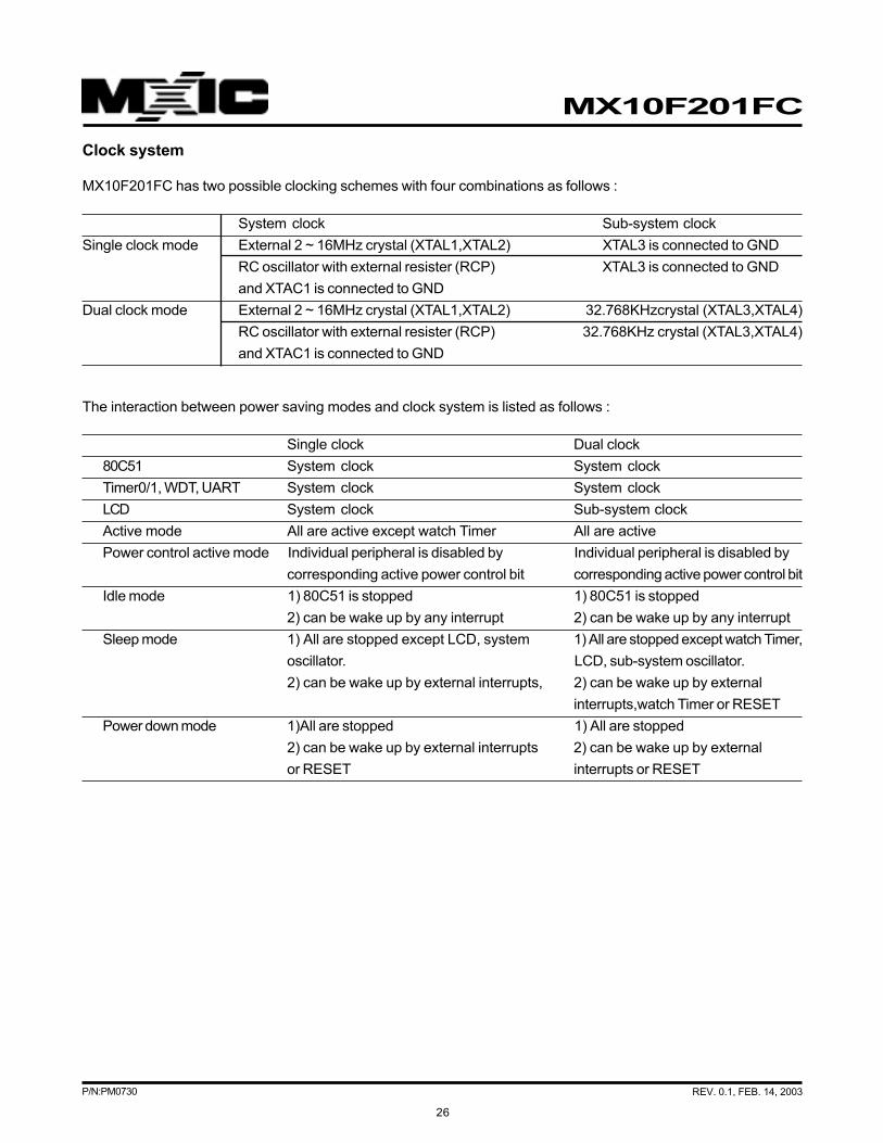
Clock system
MX10F201FC has two possible clocking schemes with four combinations as follows :
System clock Sub-system clock
Single clock mode External 2 ~ 16MHz crystal (XTAL1,XTAL2) XTAL3 is connected to GND
RC oscillator with external resister (RCP) XTAL3 is connected to GND
and XTAC1 is connected to GND
Dual clock mode External 2 ~ 16MHz crystal (XTAL1,XTAL2) 32.768KHzcrystal (XTAL3,XTAL4)
RC oscillator with external resister (RCP) 32.768KHz crystal (XTAL3,XTAL4)
and XTAC1 is connected to GND
The interaction between power saving modes and clock system is listed as follows :
Single clock Dual clock
80C51 System clock System clock
Timer0/1, WDT, UART System clock System clock
LCD System clock Sub-system clock
Active mode All are active except watch Timer All are active
Power control active mode Individual peripheral is disabled by Individual peripheral is disabled by
corresponding active power control bit corresponding active power control bit
Idle mode 1) 80C51 is stopped 1) 80C51 is stopped
2) can be wake up by any interrupt 2) can be wake up by any interrupt
Sleep mode 1) All are stopped except LCD, system 1) All are stopped except watch Timer,
oscillator. LCD, sub-system oscillator.
2) can be wake up by external interrupts, 2) can be wake up by external
interrupts,watch Timer or RESET
Power down mode 1)All are stopped 1) All are stopped
2) can be wake up by external interrupts 2) can be wake up by external
or RESET interrupts or RESET
27
P/N:PM0730 REV. 0.1, FEB. 14, 2003
MX10F201FC
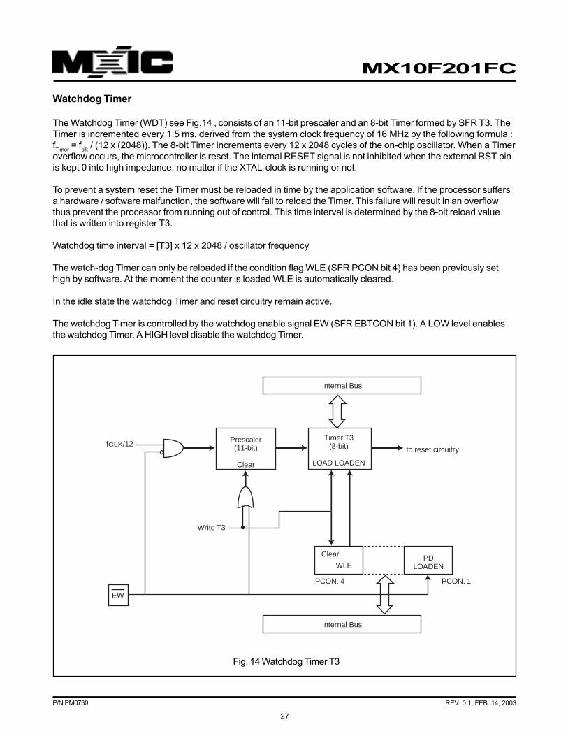
Watchdog Timer
The Watchdog Timer (WDT) see Fig.14 , consists of an 11-bit prescaler and an 8-bit Timer formed by SFR T3. The
Timer is incremented every 1.5 ms, derived from the system clock frequency of 16 MHz by the following formula :
fTimer
= fclk
/ (12 x (2048)). The 8-bit Timer increments every 12 x 2048 cycles of the on-chip oscillator. When a Timer
overflow occurs, the microcontroller is reset. The internal RESET signal is not inhibited when the external RST pin
is kept 0 into high impedance, no matter if the XTAL-clock is running or not.
To prevent a system reset the Timer must be reloaded in time by the application software. If the processor suffers
a hardware / software malfunction, the software will fail to reload the Timer. This failure will result in an overflow
thus prevent the processor from running out of control. This time interval is determined by the 8-bit reload value
that is written into register T3.
Watchdog time interval = [T3] x 12 x 2048 / oscillator frequency
The watch-dog Timer can only be reloaded if the condition flag WLE (SFR PCON bit 4) has been previously set
high by software. At the moment the counter is loaded WLE is automatically cleared.
In the idle state the watchdog Timer and reset circuitry remain active.
The watchdog Timer is controlled by the watchdog enable signal EW (SFR EBTCON bit 1). A LOW level enables
the watchdog Timer. A HIGH level disable the watchdog Timer.
Fig. 14 Watchdog Timer T3
Internal Bus
to reset circuitry
Timer T3(8-bit)
LOAD LOADEN
Internal Bus
WLEPD
LOADEN
Prescaler(11-bit)
Clear
Clear
fCLK/12
Write T3
EW
PCON. 4 PCON. 1

28
P/N:PM0730 REV. 0.1, FEB. 14, 2003
MX10F201FC
Pulse Width Modulated Outputs
The MX10F201FC contains two pulse width modulated output channels (see Figure. 15). These channels generate
pulses of programmable length and interval. The repetition frequency is defined by an 8-bit prescaler PWMP, which
supplies the clock for the counter. The prescaler and counter are common to both PWM channels. The 8-bit counter
counts modulo 255, i.e., from 0 to 254 inclusive. The value of the 8-bit counter is compared to the contents of two
registers: PWM0 and PWM1. Provided the contents of either of these registers is greater than the counter value,
the corresponding PWM0 or PWM1 output is set LOW. If the contents of these registers are equal to, or less than
the counter value, the output will be HIGH. The pulse-width-ratio is therefore defined by the contents of the
registers PWM0 and PWM1. The pulse-width-ratio is in the range of 0 to 1 and may be programmed in increments
of 1/255.
Buffered PWM outputs may be used to drive DC motors. The rotation speed of the motor would be proportional to
the contents of PWMn. The PWM outputs may also be configured as a dual DAC. In this application, the PWM
outputs must be integrated using conventional operational amplifier circuitry. If the resulting output voltages have
to be accurate, external buffers with their own analog supply should be used to buffer the PWM outputs before
they are integrated. The repetition frequency fPWM
, at the PWMn outputs is give by :
fPWM
= f
OSC
2 x (1 + PWMP) x 255
This gives a repetition frequency range of 123Hz to 31.4KHz (fOSC
= 16MHz). At fOSC
= 24MHz, the frequency range
is 184Hz to 47.1KHz. By loading the PWM registers with either 00H or FFH, the PWM channels will output a
constant HIGH or LOW level, respectively. Since the 8-bit counter counts modulo 255, it can never actually reach
the value of the PWM registers when they are loaded with FFH.
When a compare register (PWM0 or PWM1) is loaded with a new value, the associated output is updated
immediately. It does not have to wait until the end of the current counter period. Both PWMn output pins are driven
by push-pull drivers. These pins are not used for any other purpose.
The PWM function is enabled by setting SPR EBTCON bit 2,3. After reset, SFR EBTCON bit 2,3 need to be set to
use P1.4 or P1.5 as the PWM output, otherwise P1.4& P1.5 are general I/O ports.
Prescaler frequency control register PWMP Reset Value = 00H
PWMP (FEH) 7 6 5 4 3 2 1 0
MSB LSB
PWMP.0-7 Prescaler dividsion factor = PWMP +1.
Reading PWMP gives the current reload value. The actual count of the prescaler cannot be read.
Reset Value = 00H
PWM0 (FCH) 7 6 5 4 3 2 1 0
PWM1 (FDH) MSB LSB
PWM0/1.0-7} Low/high ratio of PWMn = (PWMn)
255 - ( PWMn)
EBTCON SFR (EBH) 7 6 5 4 3 2 1 0
- - - - PWM1E PWM0E /EW -
PWM1E : Selection of P1.4 function as either PWM output or a port line, After reset PWM1E bit is low, and P1.4
is a normal port line.
PWM0E : Selection of P1.5 function as either PWM output or a port line, After reset PWM0E bit is low, and P1.5
is a normal port line.
/EW : After reset, /EW bit is set, and WDT is disable.

29
P/N:PM0730 REV. 0.1, FEB. 14, 2003
MX10F201FC
Inte
rnal
Bus
PWM0
PWM0
PWM1
PWM1
PWMP
8-BIT COMPARATOR OUTPUTBUFFER
8-BIT COUNTERPRESCALER1/2
tOSC
OUTPUTBUFFER8-BIT COMPARATOR
Fig. 15 Functional Diagram of Pulse Width Modulated Outputs
30
P/N:PM0730 REV. 0.1, FEB. 14, 2003
MX10F201FC
UART
This module is fully compatible to standard 80C51's UART.

31
P/N:PM0730 REV. 0.1, FEB. 14, 2003
MX10F201FC
MTP Program Memory
Features
- 16 kilobyte electrically erasable internal MTP program momory.
- Programming and erasing voltage 12 Volt
- MTP (re) programming mechanism :
- EPROM like parallel programming protocol
- Parallel programming :
- Byte programming (8 us typical)
- Chip erase less than 0.5 second typical
- 100 minimum erase/program cycles
- Advanced CMOS flash memory technology
- One security bit to protect internal ROM code.
General Description
MX10F201FC's MTP memory stores memory contents even after 100 erase and program cycles. The cell is
designed to optimize the erase and programming mechanisms. In addition, the combination of advanced tunnel
oxide processing and low internal electric fields for erase and programming operations produces reliable cycling.
The MX10F201FC uses 12 Volt VPP supply to perform the Program/Erase algorithms.
PROGRAMMING AND PROGRAM VERIFY
MX10F201FC is byte programmable by using 10us programming pulse and it requires separate program verify
pulse to read out the data to check if program is ok or not. The typical programming time for each 1k bytes is
about 10ms at room temperature.

32
P/N:PM0730 REV. 0.1, FEB. 14, 2003
MX10F201FC
PROGRAMMING SPECIFICATION
Parallel Programming Mode
The parallel programming works in EPROM-like programming protocol. The MX10F201FC MTP provides 100 times
cycles endurance. And the MX10F201FC MTP needs a 11.5~12.5 Volt VPP supply to perform the Program/Erase
operation. Specially note that LOCK 2 is used to security protection. So if LOCK 2 bit is programmed, then PGMVFY,
ERSVFY and normal READ are disabled from parallel programming mode. LOCK 1 and LOCK 3 are not used in this
chip.
PIN NAME SYMBOL FUNCTION
P25~P20, P17~P10 PA13~PA8, PA7~PA0 Address Input
P07~ P00 Q[7:0] Data Input/Output
P33 PCEB Chip Enable Input
P27 POEB Output Enable Input
P32 PWEB Write Enable Input
VPP VPP Program Supply Voltage
P26, P37, P31, P30 MS[3:0] Flash Mode Selection
VDD VDD Power Supply Voltage (5V)
VSS GND Ground Pin
RESET
BP[3:0]
VPP
P33
P27
P32
P2[5:0] P1[7:0]
P26, P37, P31, P30
VDD
Q[7:0]
4.5/5.5V
VSS
1
0000
11.5V ~ 12.5V
PCEB
POEB
PWEB
A[13:0]
MS[3:0]
XTAL1
XTAL2
P0[7:0]
MX10F201FC
Table. 26 Pin Description

33
P/N:PM0730 REV. 0.1, FEB. 14, 2003
MX10F201FC
External EA P33 P27 P32 P2[5:0] P26, P37, P0[7:0] P0[7:0]
Pin P1[7:0] P31, P30
Module I/O PVPP PCEB POEB PWEB PA[13:0] MS[3:0] PUOUT[7:0] DI or Lock[3:1]
PDOUT[7:0] DIA
Standby 12V 1 X X X X FF,00 X
Normal Read 12V 0 0 1 PA[13:0] 0000 Data Z
Initialize 12V 0 1 0.5sec X 1110 FF,00 X 000
pulse
Chip Erase 12V 0 1 0.5sec X 0001 FF,00 X 000
pulse
Program 12V 0 1 10us PA[13:0] 0011 FF,00 D[7:0]
pulses
Erase Verify 12V 0 0 1 PA[13:0] 0100 Data Z
Program Verify 12V 0 0 1 PA[13:0] 0101 Data Z
Pgm LOCK 12V 0 1 10us PA[1:0] 0110 FF,00 X Lock[i]
pulse 0 ->1
Erase Verify 12V 0 0 1 PA[1:0]=00 1001 LOCK[3:1] Z
LOCK
Pgm Verify 12V 0 0 1 PA[1:0]=00 1011 LOCK[3:1] Z
LOCK
Read Mft ID 12V 0 0 1 PA[1:0]=00 1111 MftID(C2H) Z
Read DeviceID 12V 0 0 1 PA[1:0]=01 1111 DeviceID(0DH) Z
Table. 27 parallel programming modes
Note : 1. Program lock bits, program LOCK [1] to be 1 if PA [1:0] = 00
Program lock bits, program LOCK [2] to be 1 if PA [1:0] = 01
Program lock bits, program LOCK [3] to be 1 if PA [1:0] = 1x
2. Verify erased LOCK bits if PA [1:0] = 00
3. Verify programmed LOCK bits if PA [1:0] = 00
4. Read Manufacture ID, Device ID
PA [1:0] = 00 : Manufacture ID (C2H)
PA [1:0] = 01 : Device ID (0DH)

34
P/N:PM0730 REV. 0.1, FEB. 14, 2003
MX10F201FC
PROGRAM AND PROGRAM VERIFY FLOWCHART
START
First Address
VDD= 5VVPP = 12V
X=0
Program One10us pulse
Pass Device
Fail Device
ProgramVerify
LastAddress
Normal Read All
X=20Failx=x+1
Yes
No
YES
IncrementAddress
No
YES
Fail
Pass
35
P/N:PM0730 REV. 0.1, FEB. 14, 2003
MX10F201FC
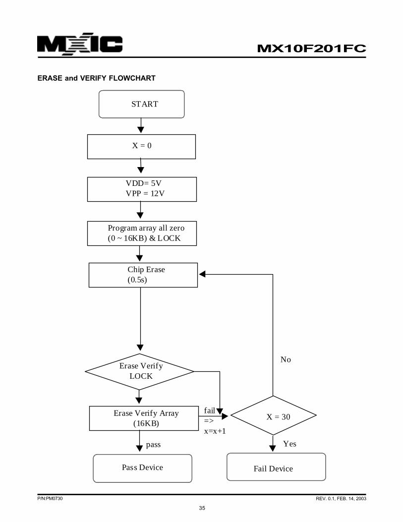
ERASE and VERIFY FLOWCHART
START
X = 0
VDD= 5VVPP = 12V
Program array all zero(0 ~ 16KB) & LOCK
Chip Erase(0.5s)
Erase VerifyLOCK
Erase Verify Array(16KB)
Pass Device
X = 30
Fail Device
fail=>x=x+1
pass Yes
No

36
P/N:PM0730 REV. 0.1, FEB. 14, 2003
MX10F201FC
PROGRAM LOCK AND PROGRAM VERIFY LOCK FLOWCHART
START
LOCK Address PA [1:0]
VDD= 5VVPP = 12V
X=0
Program LOCK10us pulse
Pass Device Fail Device
ProgramVerify LOCK
X=20Failx=x+1
Yes
No
Pass

37
P/N:PM0730 REV. 0.1, FEB. 14, 2003
MX10F201FC
A. Timing diagram of Read signature and Normal read operations
tAA tCE tOE tDF tMSCE
Min. 0 100
Max. 130 130 50 20
unit ns ns ns ns ns
A 0=0 / A 0=1
tAA
tCEtDF
OUTMfg ID / Device ID
VPP
WEB
ADDRESS
CEB
OEB
MS[3:1]
DATA
tOE
tMSCEtMSCE
38
P/N:PM0730 REV. 0.1, FEB. 14, 2003
MX10F201FC
B. Timing Diagram of Erase and Erase Verify Array Operation
tVPS tMS tCES tER tEW tEV tMSCE
Min. 2 200 100 100 0.5 100
Max. 200
unit us ns ns ns s ns ns
39
P/N:PM0730 REV. 0.1, FEB. 14, 2003
MX10F201FC
tVPS tMS tCES tER tEW tEV tMSCE
Min. 2 200 100 100 0.5 100
Max. 200
unit us ns ns ns s ns ns
C. Timing Diagram of Erase and Erase Verify LOCK Operation
40
P/N:PM0730 REV. 0.1, FEB. 14, 2003
MX10F201FC
D. Timing Diagram of Program and Program Verify Operation
tAS tDS tDH tVPS tCES tMS tPR tPW tPV tMSCE
Min. 100 100 100 2 100 200 100 8 100
Max. 200
unit ns ns ns us ns ns ns us ns ns
41
P/N:PM0730 REV. 0.1, FEB. 14, 2003
MX10F201FC
E. Timing Diagram of Program LOCK and Program Verify LOCK Operation
tAS tDS tDH tVPS tCES tMS tPR tPW tPV tMSCE
Min. 100 100 100 2 100 200 100 8 100
Max. 200
unit ns ns ns us ns ns ns us ns ns
Note : OUT = { xxxx, LOCK [3], LOCK [2], LOCK [1], x}
0110 1011
PA [1:0] PA [1:0] =00
42
P/N:PM0730 REV. 0.1, FEB. 14, 2003
MX10F201FC
Limiting Value
SYMBOL PARAMETER MIN MAX UNIT
VDD Supply voltage 4.5 5.5 V
Vi Input voltage (all inputs) -0.5 VDD + 0.5 V
VVPP
Voltage on VPP pin to VSS 0 13 V
IOL(max)
Maximum IOL per I/O pin 15 mA
Tstg Storage temperature -65 150 OC
Tamb Operating ambient temperature(for all devices) 0 70 OC
DC ELEECTRICAL CHARACTERISTICS
SYMBOL PARAMETER CONDITIONS MIN. TYP. MAX. UNIT
Supply
VDD Normal operation supply voltage 4.5 5.5 V
IDD
Operation supply current fOSC
=16MHZ 10 20 mA
fOSC
=12MHZ 8 mA
fOSC
=4MHZ 4 mA
IID
Supply current in idle mode fOSC
=16MHZ 8 12 mA
fOSC
=12MHZ 6
fOSC
=4MHZ 2
ISLP
Supply current in single sleep mode fOSC
=16MHZ 4 8 mA
fOSC
=12MHZ 3
fOSC
=4MHZ 1
IDSLP
Supply current in dual sleep mode fOSC
=16MHZ 50 100 uA
fOSC
=12MHZ 45
fOSC
=4MHZ 25
IPD
Supply current in power-sown mode fOSC
=16MHZ 1 30 uA
fOSC
=12MHZ 1
fOSC
=4MHZ 1
Inputs
RINP
Input resistance RESET VDD=4.5V to 5.5V 15 100 kohm
IL
Input leakage current; RESET VDD=5V 120 uA
VIH1
Input high voltage to 0.7VDD VDD+0.5 V
XTAL1, XTAL3, RESET
PORTS P0~P3
VIL
Input low voltage -0.5 0.2VDD-0.1 V
VIH
Input high voltage, except 0.2VDD VDD+0.5 V
XTAL1, XTAL3, RST +0.9
IIL
Logical 0 input current VIN=0.4V, VDD=5V -1 -100 uA
ITL
Logical 1 to 0 transition current VIN=2.0V -650 uA
43
P/N:PM0730 REV. 0.1, FEB. 14, 2003
MX10F201FC
Outputs : P0~P3
SYMBOL PARAMETER CONDITIONS MIN. TYP. MAX. UNIT
VOL
Output low voltage VDD=4.5V, IOL
=1.6mA 0.4 V
VOH
Output high voltage VDD=4.5V, IOH
=- 3.3mA VDD-0.7 V
IOL
Low level output sink current VO<0.4V, VDD=5V 10 13 mA
IOH
High level pull-up output source current
Strong pull-up VO=VDD-0.4V, VDD=5V 4 6 mA
Weak pull-up VO=VDD-0.4V, VDD=5V 15 30 uA
CIO
Pin capacitance (except EA) 15 pF
SYMBOL PARAMETER CONDITIONS MIN. TYP. MAX. UNIT
Supply
VLCD LCD operation supply voltage 4.5 VDD V
VSS DC voltage component; all backplane 100 mV
and segment drivers
LCD driver outputs
RBP
Output impedance BP0~BP3 6 20 kohm
RS
Output impedance S0~S31 6 20 kohm
fLCD
LCD scan frequency Ratio: 1:1, 1:2, 1:4 61 Hz
Ratio: 1:3 81 Hz
LCD DRIVER CHARACTERISTICS
44
P/N:PM0730 REV. 0.1, FEB. 14, 2003
MX10F201FC
5.5 5 4.5 3.3 3 2.7
100kohm 9.36 9.19 8.7 7.4 6.48 6.15
40kohm 15.98 14.81 14.29 10.95 10.12 8.99
20
15
10
5
0
5.5 5 4.5 3.3 3 2.7
100Kohm
40Kohm
MHz
V
Fosc - Vdd
RCP OSCILLATOR CHARACTERISTICS
AC CHARACTERISTICS
SYMBOL PARAMETER CONDITIONS MIN. TYP. MAX. UNIT
System (CPU) clock
fC Oscillator frequency 2 16 MHz
32.768KHz LCD Oscillator
fxtal
32.768KHz Oscillator frequency 32.768 KHz
45
P/N:PM0730 REV. 0.1, FEB. 14, 2003
MX10F201FC
PACKAGE INFORMATION100-PIN PQFP
A
B
E C D
IHG
F 1 3031
505180
81
100
N
M
J
K
L
P
O
ITEM MILLIMETERS INCHES
A 24.80 ± .40 .976 ± .016
B 20.00 ± .13 .787 ± .005
C 14.00 ± .13 .551 ± .005
D 18.80 ± .40 .740 ± .016
E 12.35 [REF] .486 [REF]
F .83 [REF] .033 [REF]
G .58 [REF] .023 [REF]
H .30 [Typ.] .012 [Typ.]
I .65 [Typ.] .026 [Typ.]
J 2.40 [Typ.] .094 [Typ.]
K 1.20 [Typ.] .047 [Typ.]
L .15 [Typ.] .006 [Typ.]
M .10 max. .004 max.
N 2.75 ± .15 .108 ± .006
O .10 min. .004 min.
P 3.30 max. .130 max.
NOTE: Each lead centerline is located within.25mm[.01 inch] of its true position [TP] at amaximum material condition.
46
P/N:PM0730 REV. 0.1, FEB. 14, 2003
MX10F201FC
REVISION DESCRIPTION PAGE DATE
0.1 Modify Table. 15 INTCON SFR (C8H) --> (C0H) P14 SEP/06/2002
MACRONIX INTERNATIONAL CO., LTD.HEADQUARTERS:TEL:+886-3-578-6688FAX:+886-3-563-2888
EUROPE OFFICE:TEL:+32-2-456-8020FAX:+32-2-456-8021
JAPAN OFFICE:TEL:+81-44-246-9100FAX:+81-44-246-9105
SINGAPORE OFFICE:TEL:+65-348-8385FAX:+65-348-8096
TAIPEI OFFICE:TEL:+886-2-2509-3300FAX:+886-2-2509-2200
MACRONIX AMERICA, INC.TEL:+1-408-453-8088FAX:+1-408-453-8488
CHICAGO OFFICE:TEL:+1-847-963-1900FAX:+1-847-963-1909
http : //www.macronix.com
MACRONIX INTERNATIONAL CO., LTD. reserves the right to change product and specifications without notice.
MX10FM201FC