multiple-scattering theoretical approach to scanning ... · multiple-scattering theoretical...
TRANSCRIPT
Multiple-scattering theoretical approach to scanning tunneling microscopy
Kamal K. Saha,* Jürgen Henk, Arthur Ernst, and Patrick BrunoMax-Planck-Institut für Mikrostrukturphysik, Weinberg 2, D-06120 Halle (Saale), Germany
�Received 25 June 2007; revised manuscript received 14 October 2007; published 25 February 2008�
An approach for computing scanning tunneling microscopy from first principles is proposed. Within theframework of Landauer-Büttiker theory, the conductance of a scanning tunneling microscope �STM� is ob-tained in terms of real-space Green functions, thereby taking into account incoherent tunneling processes andthe tip-sample interaction but avoiding repeated STM tips as in a supercell approach. The approach is formu-lated within multiple-scattering theory, especially in the Korringa-Kohn-Rostoker method, but can be imple-mented in any Green-function method for electronic-structure calculations. Extensive tests are presented forplanar and STM tunnel junctions involving Au�111� electrodes.
DOI: 10.1103/PhysRevB.77.085427 PACS number�s�: 68.37.Ef, 72.10.�d, 73.40.Gk
I. INTRODUCTION
The invention of the scanning tunneling microscope�STM� by Binnig and Rohrer �see Ref. 1 for a review� was arevolution in surface physics. The ability to probe locallysurfaces and adsorbates on the atomic scale led to new ex-perimental methods and new insights that were impossible toobtain by other advanced methods �such as photoelectronspectroscopy or low-energy-electron diffraction�.2 In order tointerpret STM experiments qualitatively and quantitatively,there have been numerous efforts to formulate a theory of theSTM,3 preferably within the framework of first-principleselectronic-structure calculations.
The probably most widely used model was proposed byTersoff and Hamann4,5 �TH� who, applying the transfer-Hamiltonian approach of Bardeen,6 express the tunnel cur-rent by the density of states of the sample at the position ofthe STM tip. By this means, the tunnel current becomes in-dependent of the electronic properties of the tip. This featureobviously contradicts experiments that find indeed a depen-dence of the tunnel current on the tip and its preparationconditions. Astonishingly, the TH model works well pro-vided the surface density of states is computed by advancedfirst-principles methods, such as the full-potential linearizedaugmented plane wave or the full-potential Korringa-Kohn-Rostoker �KKR� method.7 For example, the corrugation andthe magnetic contrast in spin-resolved STM �see, e.g., Ref.8� agree qualitatively and semiquantitatively with experi-mental results �without any claim of completeness, we referto Refs. 9–14�.
However, the TH model approximates crudely the tunnelmatrix elements that can essentially determine the tunnel cur-rent. A step beyond the TH model is the transfer-Hamiltonianapproach in which the matrix elements are computed fromthe wave functions of the sample and the tip.15,16 In order todistinguish unequivocally the tip wave function from thesample wave function, the entire tunnel junction is dividedinto two subsystems, namely, the sample and tip, and theelectronic structures of these subsystems are calculated sepa-rately. Therefore, tip-sample interactions, which might besignificant for small tip-sample distances, are not included.17
Both of the above-mentioned theories rely solely on theelectronic structures of sample and tip but neglect the bound-
ary conditions, in particular reservoirs attached to the leads.Tunneling is a scattering process and, hence, scatteringboundary conditions have to be applied, as is done in theLandauer-Büttiker theory of electronic transport. Within thisrespect, the conductance of a tunnel junction can be viewedas transmission.18 One particular way to obtain the transmis-sion probability can be regarded as the “electron-counting”picture: the conductance is proportional to the rate at whichelectrons are transmitted from one lead to the other. To ob-tain this rate, the electrons in the reservoirs are counted be-fore and after establishing a connection of the otherwise dis-connected leads. This approach can be formulated via theGreen functions of the decoupled and coupled subsystems�see Sec. II C�.
The above Landauer-Büttiker approach has a number ofadvantages as compared to other approaches. �i� It considersthe role of reservoirs and obeys scattering boundary condi-tions. �ii� The electronic structures of both leads and tunnelbarrier are fully taken into account. Since an ab initio calcu-lation is performed for the entire tunnel junction, the effectof tip-sample interactions is fully accounted for, in contrastto the Bardeen approach. �iii� By solving the Dyson equationfor the STM tip in real space �configuration space�, a systemwith a single tip is treated. This feature is different fromsupercell approaches in which an artificial periodicity mightlead to spurious errors due to “cross talk” between adjacentSTM tips.19,20 �iv� It can be implemented in a variety ofmethods for electronic-structure calculations which rely onGreen functions, in particular tight-binding and multiple-scattering methods. We note in passing that Green functionsprovide a means to incorporate substitutional disorder via thecoherent potential approximation.21–23
In order to implement the outlined approach for a STM, acomputational scheme is needed that can deal with largesystems.24 Besides tight-binding methods, multiple-scattering theory is an obvious choice. �We would like tomention explicitly the tight-binding or screened versions ofthe KKR method25–28 and of the linear muffin-tin orbitalmethod.29� The latter has proven its suitability for treating avariety of problems with high accuracy; to name a few, bulkand surface electronic properties, electron spectroscopiessuch as low-energy-electron diffraction and photoelectronspectroscopy, substitutional disorder in alloys, etc.30 The ac-curacy, as high as for other advanced methods, is evident, for
PHYSICAL REVIEW B 77, 085427 �2008�
1098-0121/2008/77�8�/085427�12� ©2008 The American Physical Society085427-1
example, from computations of the magnetic anisotropy ofultrathin films31,32 and of the dispersion of surface states.33,34
With this background in mind, a multiple-scattering theory ofscanning tunneling microscopy was implemented in a spin-polarized relativistic layer KKR computer code, which is de-scribed and applied in the present paper. Although the num-ber of advantages is significant �see previous paragraph�, noapproach is, of course, without shortcomings. These are dis-cussed in Sec. II D. We would like to emphasize that theapproach is not restricted to tunneling through a vacuumbarrier; transport in nanocontacts �e.g., atomic point contactsor nanowires� can be treated as well.
The paper is organized as follows. The basic theory isoutlined in Sec. II, sketching a KKR formulation of the con-ductance calculations in real space. The scheme is applied toscanning tunneling spectroscopy on Au�111�,35,36 addressingin particular the effect of a STM tip on the conductance. Thepaper concludes with remarks given in Sec. IV.
II. THEORY
A. Introductory remarks
Since the following sections are rather technical, it ap-pears helpful to start with a brief outline of the approach. Ascanning tunneling microscope can be viewed as built fromthree subsystems: the ideal leads of the sample and of the tipside, respectively, and the tunnel barrier, which comprisesthe STM tip and the lead surfaces. These subsystems arejoined at so-called decoupling—or coupling—regions L andR �L and R stand for the left and right decoupling regions,respectively�. Since Landauer-Büttiker theory will be ap-plied, for each of the steps discussed below two Green func-tion �GFs� have to be computed: one for the system withdecoupled subsystems, the other for the system with coupledsubsystems �cf. the electron-counting picture mentioned inSec. I�.37 The conductance of the STM is computed in realspace from the final GFs.
The computational procedure is as follows. �i� Greenfunctions are computed in reciprocal space for tunnel junc-tions with decoupled and coupled subsystems. These systemsdo not include the STM tip and, thus, are translationallyinvariant parallel to the layers. Hence, the in-plane wave vec-tor k� is a good quantum number. �ii� These Green functionsare expressed as real-space GFs in a finite cluster, i.e., for afinite number of unit cells in each layer, using lattice Fouriertransformation. �iii� Regarding the STM tip as a local pertur-bation �loosely speaking a “defect” or “impurity”�, the STMtip is eventually introduced by solving the Dyson equationfor the defect potentials �that form the STM tip� in the clus-ter. Hence, translational invariance is lost. �iv� The conduc-tance in the finite cluster around the STM tip is computedfrom the GFs obtained in step �iii�.
The transformation from reciprocal to configurationalspace is necessary because the conductance is obtained for atunnel junction with a single STM tip �no translational in-variance�. In contrast, a supercell approach computes in re-ciprocal space the conductance of infinitely repeated cells,each containing a STM tip. Both approaches become equiva-lent in the limit of infinitely large supercells.
B. KKR Green functions
The following derivations and considerations rely heavilyon KKR theory. For brevity, the reader is referred to Refs.38–40 and 30 for details. A brief introduction to typical layerKKR algorithms is given in Ref. 41.
For simplicity we restrict ourselves to the case of oneatom per layer unit cell. It is straightforward to extend thetheory to more atoms per cell. Note that in layer KKR�LKKR� method all layers have identical sets �Ri� of trans-lation vectors, so these need not be indicated by a layer in-dex. In the following, layers and cells are denoted by upper-case and lower-case letters, respectively. Further, thecomplex “energy” z at which the GFs are evaluated isdropped.
The starting point is a system that is translationally invari-ant parallel to the layers, that is, it has two-dimensional �2D�periodicity �no STM tip�. Hence, the electronic states arecharacterized by the in-plane wave vector k�. A KKR Greenfunction G comprises two parts, a single-site part and amultiple-scattering part. The compact form of the single-sitepart is explicitly given by
��
r�0IZ�
R0I�J�L0Ir��
0I�
� �� r0IZ�
R0I�J�L0Ir�0I� , r0I � r�0I,
r0IJ�R0I�Z�
L0Ir�0I� , r0I � r�0I,�1�
where r0I is a vector within unit cell 0 of layer I. r�0I �r�
0I�denotes the smaller �larger� of r0I and r�0I. The spin-angularmulti-indices � comprise the angular momentum and spinquantum numbers, e.g., �= ���� in the relativistic case42,43
or �= �lm�� in the nonrelativistic case. Z�R0I� and J�
R0I� areright-hand-side �RHS� �superscript R� regular and irregularscattering solutions of the �muffin-tin� potential located incell 0 of layer I, respectively. The corresponding LHS scat-tering solutions are superscribed by L.44
The propagation of an electron from cell 0 in layer J tocell 0 in layer I is mediated by the scattering-path operator,with matrix elements ����
0I;0J. It accounts for all scatteringpaths within the system. The complete GF then reads
G�r0I,r�0J;k�� = ����
r0IZ�R0I�����
0I;0J�k��Z��L0Jr�0J�
− ��
r�0IZ�
R0I�J�L0Ir��
0I�0I;0J. �2�
The Kronecker means iI;iJ=ijIJ. Note that the GF obeysthe Bloch theorem,
G�riI,r�0J;k�� = eik�·RiG�r0I,r�0J;k�� , �3�
for any translation vector of the layer lattice. Ri is the trans-lation vector from cell 0 to cell i, and riI=r0I+Ri.
To shorten the notation, scattering solutions andscattering-path operators are combined into vectors and ma-trices indexed by �,
�ZR0I�� � Z�R0I� , �4a�
SAHA et al. PHYSICAL REVIEW B 77, 085427 �2008�
085427-2
�ZL0I�� � Z�L0I , �4b�
��0I;0J�k������ � ����0I;0J�k�� . �4c�
Note that ZR0I �ZL0I� is a column �row� vector. Hence, Eq. �2�becomes
G0I;0J�k�� = ZR0I�0I;0J�k��ZL0J − ZR0IJL0I0I;0J. �5�
Having determined the reciprocal-space GF of the trans-lationally invariant system, it is transformed into real-spacerepresentation using the lattice Fourier transformation,
�iI;jJ =1
�
2BZeik�·�Ri−Rj��0I;0J�k��d2k� . �6�
is the area of the two-dimensional Brillouin zone �2BZ�.The inverse Fourier transformation is given by
�0I;0J�k�� =1
T�ij
e−ik�·�Ri−Rj��iI;jJ, �7�
where T is the order of the translation group of the layerlattice. The real-space GF then reads
GiI;jJ = ZR0I�iI;jJZL0J − ZR0IJL0IiI;jJ �8�
and obeys
G�i+1�I;�j+1�J = GiI;jJ �9�
due to 2D translational invariance.In the final step of the computation of the GF, the STM tip
is introduced. If we consider the STM tip as a local pertur-bation �i.e., a defect or an impurity�, it alters the scatteringpotentials in a finite region in the vicinity of the tip and,hence, breaks the translational invariance parallel to the lay-ers. Note in particular that the potentials of the leads, i.e., faraway from the tunnel barrier, remain unchanged. Thus, thedefect region, denoted by D, comprises a finite set of cell �l�and layer �L� indices �D= �lL� is located between L and R,
all regions being disjunct�. The Green function G of the sys-tem with STM tip is obtained from the Dyson equation,
G = G + G�VG , �10�
where �V is the potential of the perturbation �quantities ofsystems with the STM tip are decorated by a tilde�. Thisequation translates in the KKR formalism to
GiI;jJ = GiI;jJ + �lL�D
GiI;lL�tlL − tlL�GlL;jJ, �11�
which can be solved exactly.45 tlL and tlL are the single-sitescattering matrices of the systems with and without STM tip,respectively. In contrast to Eq. �8�, the scattering solutions in
G carry a cell index because the potentials, the scatteringsolutions, and hence the single-site scattering matrices, de-pend on the cell,
GiI;jJ = ZRiI�iI;jJZLjJ − ZRiIJLiIiI;jJ. �12�
Eventually, the Green functions G for the decoupled and thecoupled systems are used to compute the conductance of theSTM.
C. Computation of the conductance
For the computation of the conductance of the STM,Landauer-Büttiker theory is applied. Within the electron-counting picture of transport, the conductance C of the STMjunction is obtained from the transmission probabilities of allscattering channels incoming in one lead and outgoing in theother lead,18
C�V� = G0��V� , �13�
where V is the applied bias voltage. The conductance quan-tum G0=e2 /h is the inverse von Klitzing constant �i.e., thequantum of resistance, RK�25.8 k�. The total transmit-tance ��V� comprises the transmission probabilities in the“energy window of tunneling” opened by V.46 For zero biasvoltage �V=0, linear response�, which is the case consideredin this paper, only the transmittance at the common Fermienergy EF of the two leads needs to be considered. Since theenergy is fixed in the following, it is dropped in the equa-tions.
The transmission probabilities can be computed from theGFs of a system in which the tunnel barrier is first decoupledfrom the leads and subsequently coupled to the leads. Withina tight-binding approach, the decoupling can be achieved bysetting the hopping matrix elements between barrier andleads to zero.47,48 Or an “impermeable membrane” betweenthe two leads could be erected.49 In the KKR approach,where the scattering potentials can easily be accessed, thedecoupling can be achieved by erecting high potential wallsof sufficiently large width between leads and tunnel barrier.37
Although a residual coupling remains, tuning the height andwidth of the potential walls allows conductances to be ob-tained as accurately as in other sophisticated KKRapproaches.50
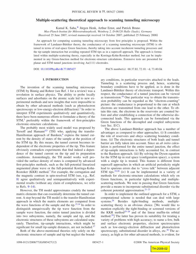
The decoupling regions in which the potential walls areerected are denoted by L and R �Fig. 1�. The real-space
FIG. 1. �Color� Schematic representation of a STM. The left partshows the sample electrode, with the decoupling region L in green.The STM tip with its lead and its decoupling region R �also ingreen� is shown on the right. The closed-path summations in Eq.�19� are performed over all pairs of sites in the decoupling regions.One such closed path is shown in red. The site potentials of thedecoupled and the coupled systems differ only in the two decou-pling regions.
MULTIPLE-SCATTERING THEORETICAL APPROACH TO… PHYSICAL REVIEW B 77, 085427 �2008�
085427-3
Green function of the system with the tunnel barrier decou-pled from the leads is given by �subscript “dc”�
GdciI;jJ = Zdc
RiI�iI;jJZdcLjJ − Zdc
RiIJdcLiIiI;jJ, �14�
with scattering-path operator �. Analogously, that of thecoupled system �subscript “c”� reads
GciI;jJ = Zc
RiI�iI;jJZcLjJ − Zc
RiIJcLiIiI;jJ, �15�
with scattering-path operator �.For a translationally invariant system �e.g., a planar tunnel
junction; cell index in principle unnecessary� the transmit-tance ��k�� at a particular wave vector can be obtained from
��k�� = �IJ�L
�KL�R
�IJ;KL�k�� , �16�
with
�IJ;KL�k�� = �t0I��0I;0J�k�� − �0J;0I�k��†��t0J†�0J;0K�k��
�t0K��0K;0L�k�� − �0L;0K�k��†��t0L†�0I;0L�k��†.
�17�
Here, �t0I is the difference of the single-site scattering ma-trices of the coupled and the decoupled system. The summa-tion runs over all layers in the decoupling regions L and R.Note further that the above matrices have to be obtained veryclose to the real energy axis, that is, the side limits of theGFs have to be considered.38
Equations �13�, �16�, and �17� are the KKR analog to theLandauer conductance formula51
C = G0 Tr�Im��L�G Im��R�G†� , �18�
where the Green function G propagates an electron from theright to the left lead. This is accomplished in KKR theory bythe scattering-path operator �SPO� � in Eq. �15�. The self-energies �L and �R account for the decoupling of the leadsand the barrier. Their imaginary parts translate in the KKRapproach into terms like �t0I��0I;0J�k��−�0J;0I�k��†��t0J† �cf.Eq. �17��.
It is straightforward, using the lattice Fourier transform�Eqs. �6� and �7��, to obtain an expression for the conduc-tance in real space. For � one gets
� =1
T�
iI;jJ�L�
kK;lL�R�tiI��iI;jJ − � jJ;iI†��t jJ†� jJ;kK�tkK
��kK;lL − �lL;kK†��tlL†�iI;lL†. �19�
The prefactor 1 /T appears due to the translational invariance,implying that � is the transmittance per cell. Note furtherthat any scattering-path operator for this system obeys �iI;jJ
=��i+1�I;�j+1�J. We would like point out that each term in theabove sum specifies a closed path in real space �Fig. 1�.
The loss of translational invariance �due to the STM tip�imposes the question of how to identify the effect of theSTM tip on the conductance, as compared to that of a planartunnel junction �PTJ�. For a translationally invariant system,namely, a PTJ, one defines a transmittance per cell, as in Eq.�19�. Evidently, the total transmittance is infinite due to theinfinite number of cells through which the current flows. Ac-
cordingly, the total transmittance of a STM is infinite, too.In order to identify uniquely the difference of the conduc-
tances of the STM and PTJ we proceed as follows. The sumsin Eq. �19� run over the infinite number of cells in regions Land R. The real-space cluster cuts out a finite subset of theinfinite cell set, denoted by C. Hence, the total transmittanceof a PTJ can be expressed as
�tot = ��C� + ��C� . �20�
��C� comprises all conductance paths that lie within C �Fig.
1�, whereas ��C� contains all other paths. With Eq. �19�, one
has �tot=T�, and both �tot and ��C� become infinite if theorder of the translation group T→�. For a STM one hasaccordingly
�tot = ��C� + ��C� . �21�
If the cluster C is sufficiently large �which needs to bechecked by convergence tests; see Sec. III A�, one has
��C����C�. The transmittance difference, that is, the ef-fect of the STM tip, is then given by
�� = �tot − �tot � ��C� − ��C� . �22�
The knowledge of both �� and � from Eq. �19� allows oneto investigate the effects of tip-sample interaction and ofelectronic states localized at the STM tip. We note in passingthat �� can be calculated directly from the transmittances �
and � of the PTJ and the STM. Another way is to express�� in terms of the Green function of the barrier �with SPOs� and ��, since these are related by a Dyson equation for theSTM tip region �similar to Eq. �11��, and use that expressionin the numerical computation. In the present paper, the con-ductance of the STM is obtained from Eqs. �19� and �22� butfor the SPOs and single-site t matrices obtained by solving
the Dyson equation for the tip region, that is, with �, �, etc.
D. Discussion of approximations
The proposed approach relies on the 2D lattice Fouriertransformation, in order to compute the real-space KKRGreen function. This implies that a 2D periodicity is inherentto the entire system, including both electrodes. In otherwords, each layer has to have identically shaped unit cells.
In a practical computation, several restrictions apply dueto limitations of computer memory and computation time. Afirst problem is the accurate determination of the real-spaceGFs from the reciprocal-space GFs �Eqs. �6� and �8��. Re-gardless of whether an equidistant k� mesh, for example spe-cial points,52 or an adaptive integration method53 is used, fora correct description of the electronic structure the number ofk� needed is on the order of several 1000 to several 10 000wave vectors. Note in this respect that KKR GFs have to becomputed for complex energies, the imaginary part of whichis chosen on the order of meV or �eV.
A second problem appears due to the finite size of thereal-space cluster C. In principle, the conductance of theentire surface-tip system needs to be computed, which isobviously impossible. Thus, the summations in Eq. �19� over
SAHA et al. PHYSICAL REVIEW B 77, 085427 �2008�
085427-4
L and R have to be restricted to a finite cluster C surround-ing the STM tip, the size of which has to be determined byconvergence tests �see also Ref. 54�. A finite cluster is suffi-cient because in a STM the current flows almost exclusivelythrough the STM tip �“eye of the needle”� and proceeds in acone with finite opening angle.55–58 The other regions �whichcan be viewed as parts of a planar tunnel junction with awide vacuum barrier� contribute much less to the conduc-tance. This will be elucidated by the convergence tests pre-sented in Sec. III A.
The Landauer-Büttiker theory assumes the transmissionof Bloch states of the leads �scattering boundary conditions�computed infinitely far from the tunnel junction. Here, athird problem arises from the fact that the summation overthe decoupling regions L and R in the conductance calcula-tion is not performed infinitely far from the tunnel barrier buttypically rather close to the surface of the leads �Fig. 1�.54
Thus, the conductance might be influenced by the surfaceelectronic structure, in particular by surface states which de-cay slowly toward the bulk �as is, for example, the case34 forAu�111��. The effect of the surface electronic structure canbe determined by comparing the conductances for the planartunnel junction �without STM tip� obtained with the Bloch-wave transmission approach by MacLaren and co-workers50
�which by construction does not include surface contribu-tions� and the present approach.
Since the decoupling is achieved by potential walls offinite height in a finite number of layers, there remains aresidual coupling which in principle can be made negligiblysmall. It turns out that typically a minimum of four layerswith potentials of 2 Hartree height are sufficient. Note thatthe decoupling can be checked by computing the conduc-tance of a bare lead, i.e., a system entirely built of a singleideal lead. In this case, the transmission probability mustequal the number of scattering channels �Sharvinconductance59�.
Another problem when implementing a new approach isto test its accuracy. For planar tunnel junctions, we haveimplemented the Bloch-wave transmission approach,50 anapproach based on the Kubo-Greenwood formula for theconductivity tensor,60–62 and the present GF approach in ourmodular LKKR computer code.37 It was shown for theformer and latter approaches that these give almost identicalresults, even for complex systems �e.g., Fe /MgO /Fe withFeO interfaces�.63 The latter method37 is the basis for thereal-space STM approach presented here. The LKKR com-puter code was extended to deal with clusters in real spaceand with the Dyson equation. All these parts were crosschecked with other KKR codes and tested for other compu-tational modes �such as, for example, Bloch spectral densi-ties and density of states�.
Recently, a GF approach for the STM was implementedby Blanco et al. �see Ref. 20 and references therein�. Al-though similar to the approach presented here, it relies on aslab calculation involving supercells rather than treatingsemi-infinite leads and a single STM tip. An advantage ofthat implementation is that relaxations of both the surfaceand the tip atoms can be taken into account. In favor of ourapproach, we would like to note that, in principle, relaxationscan be treated as well by solving a Dyson equation for the
atoms displaced from their ideal positions �see, for example,Refs. 64 and 65�. This would allow to investigate the effectof tip-induced relaxations on the tunneling conductance.66,67
A nonequilibrium Green function approach for calculatingthe electronic transport of atomic-scale systems was de-scribed by Brandbyge et al.68 The scattering region is definedwithin a finite supercell and consequently the GF matrixmight not be sufficiently large to minimize interference ef-fects. The latter are induced by the repeated images of theSTM tip. However, the indisputable advantage of thismethod is that the charge-density matrix is clearly expressedin two parts, i.e., an equilibrium and a nonequilibrium con-tribution. The technique can thus be extended to multitermi-nal devices.
In the present work we focus on the conductance for zerobias voltage. An extension to finite bias could be performedwithin the framework of nonequilibrium Green functions orby assuming a heuristic voltage drop within the vacuum bar-rier �typically a linear dependence, as, e.g., in Refs. 46 and69–71�. Both approaches have already been applied success-fully. In particular, it can be shown that a multiple-scatteringtheory based on nonequilibrium Green functions systemati-cally corrects the Bardeen formalism for nonzero biasvoltage.72 The latter allows, in particular, the sample and thetip contributions to the conductance to be distinguished,73 asopposed to the Landauer-Büttiker formalism.
E. Size and shape of the real-space cluster
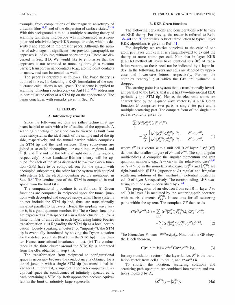
A conductance calculation for a tunnel junction �either aplanar or a STM junction� is computationally demanding.But if the chosen method is a real-space approach it is evenmore demanding. Therefore, it is desirable to reduce thenumber of cells in the cluster as far as possible but withoutperceptible loss of accuracy. Further, the shape of the clusterhas to be chosen appropriately, keeping in mind the “bottle-neck” picture behind the STM tip. By this means a lot ofcomputer memory and computational time can be saved.
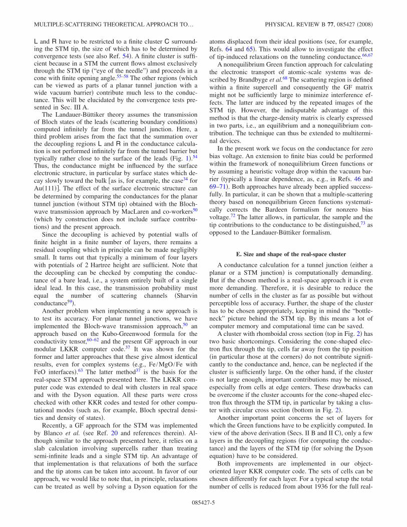
A cluster with rhomboidal cross section �top in Fig. 2� hastwo basic shortcomings. Considering the cone-shaped elec-tron flux through the tip, cells far away from the tip position�in particular those at the corners� do not contribute signifi-cantly to the conductance and, hence, can be neglected if thecluster is sufficiently large. On the other hand, if the clusteris not large enough, important contributions may be missed,especially from cells at edge centers. These drawbacks canbe overcome if the cluster accounts for the cone-shaped elec-tron flux through the STM tip, in particular by taking a clus-ter with circular cross section �bottom in Fig. 2�.
Another important point concerns the set of layers forwhich the Green functions have to be explicitly computed. Inview of the above derivation �Secs. II B and II C�, only a fewlayers in the decoupling regions �for computing the conduc-tance� and the layers of the STM tip �for solving the Dysonequation� have to be considered.
Both improvements are implemented in our object-oriented layer KKR computer code. The sets of cells can bechosen differently for each layer. For a typical setup the totalnumber of cells is reduced from about 1936 for the full real-
MULTIPLE-SCATTERING THEORETICAL APPROACH TO… PHYSICAL REVIEW B 77, 085427 �2008�
085427-5
space cluster to 264 for the improved one. This correspondsto a reduction of computer memory from about 25 to about1.2 Gbytes.
F. Computation
The electronic properties of the tunnel junctions discussedin Sec. III were obtained within the local spin-density ap-proximation to density-functional theory, using a multicodeapproach. The ab initio calculations are performed with theKKR code HUTSEPOT, details of which can be found in Refs.74–77. The generated self-consistent potentials serve as in-put for the conductance calculations, using the spin-polarizedrelativistic layer KKR code OMNI2K. The latter is focused onthe computation of electron spectroscopy, rather than on per-forming ab initio calculations. It solves the Dirac equationfor the single-site problem, and spin-orbit coupling is in-cluded in both the electronic-structure and the transport cal-culations.
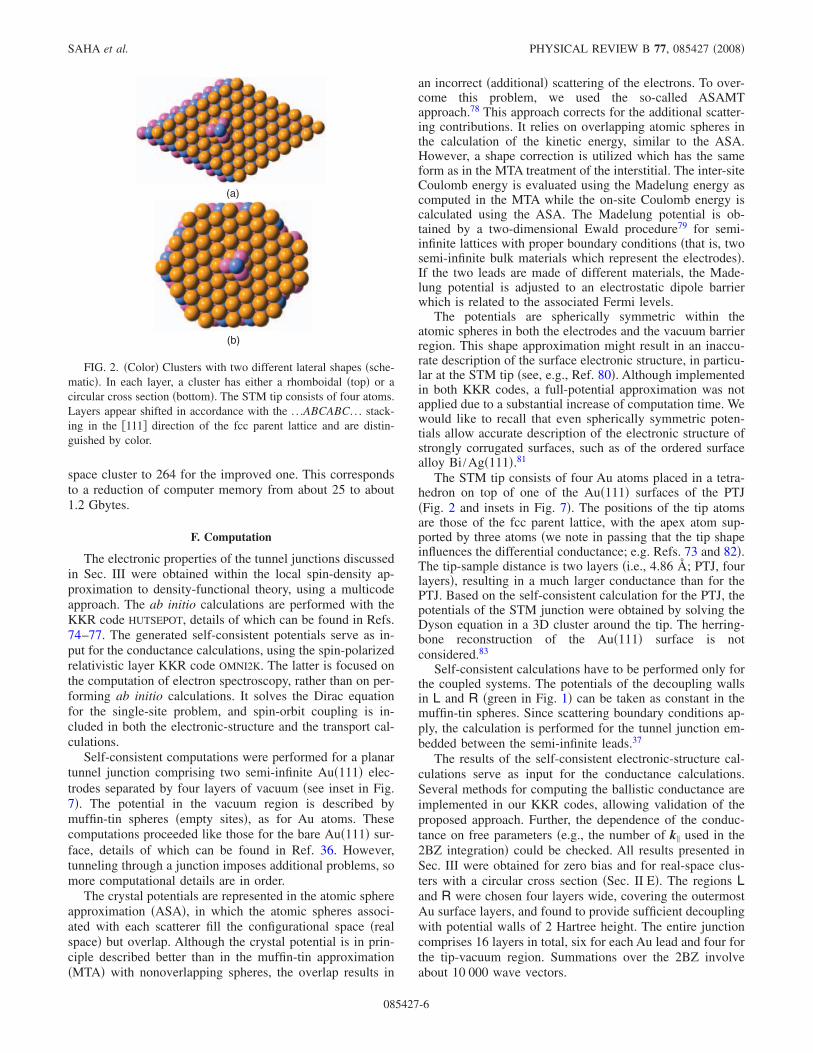
Self-consistent computations were performed for a planartunnel junction comprising two semi-infinite Au�111� elec-trodes separated by four layers of vacuum �see inset in Fig.7�. The potential in the vacuum region is described bymuffin-tin spheres �empty sites�, as for Au atoms. Thesecomputations proceeded like those for the bare Au�111� sur-face, details of which can be found in Ref. 36. However,tunneling through a junction imposes additional problems, somore computational details are in order.
The crystal potentials are represented in the atomic sphereapproximation �ASA�, in which the atomic spheres associ-ated with each scatterer fill the configurational space �realspace� but overlap. Although the crystal potential is in prin-ciple described better than in the muffin-tin approximation�MTA� with nonoverlapping spheres, the overlap results in
an incorrect �additional� scattering of the electrons. To over-come this problem, we used the so-called ASAMTapproach.78 This approach corrects for the additional scatter-ing contributions. It relies on overlapping atomic spheres inthe calculation of the kinetic energy, similar to the ASA.However, a shape correction is utilized which has the sameform as in the MTA treatment of the interstitial. The inter-siteCoulomb energy is evaluated using the Madelung energy ascomputed in the MTA while the on-site Coulomb energy iscalculated using the ASA. The Madelung potential is ob-tained by a two-dimensional Ewald procedure79 for semi-infinite lattices with proper boundary conditions �that is, twosemi-infinite bulk materials which represent the electrodes�.If the two leads are made of different materials, the Made-lung potential is adjusted to an electrostatic dipole barrierwhich is related to the associated Fermi levels.
The potentials are spherically symmetric within theatomic spheres in both the electrodes and the vacuum barrierregion. This shape approximation might result in an inaccu-rate description of the surface electronic structure, in particu-lar at the STM tip �see, e.g., Ref. 80�. Although implementedin both KKR codes, a full-potential approximation was notapplied due to a substantial increase of computation time. Wewould like to recall that even spherically symmetric poten-tials allow accurate description of the electronic structure ofstrongly corrugated surfaces, such as of the ordered surfacealloy Bi /Ag�111�.81
The STM tip consists of four Au atoms placed in a tetra-hedron on top of one of the Au�111� surfaces of the PTJ�Fig. 2 and insets in Fig. 7�. The positions of the tip atomsare those of the fcc parent lattice, with the apex atom sup-ported by three atoms �we note in passing that the tip shapeinfluences the differential conductance; e.g. Refs. 73 and 82�.The tip-sample distance is two layers �i.e., 4.86 Å; PTJ, fourlayers�, resulting in a much larger conductance than for thePTJ. Based on the self-consistent calculation for the PTJ, thepotentials of the STM junction were obtained by solving theDyson equation in a 3D cluster around the tip. The herring-bone reconstruction of the Au�111� surface is notconsidered.83
Self-consistent calculations have to be performed only forthe coupled systems. The potentials of the decoupling wallsin L and R �green in Fig. 1� can be taken as constant in themuffin-tin spheres. Since scattering boundary conditions ap-ply, the calculation is performed for the tunnel junction em-bedded between the semi-infinite leads.37
The results of the self-consistent electronic-structure cal-culations serve as input for the conductance calculations.Several methods for computing the ballistic conductance areimplemented in our KKR codes, allowing validation of theproposed approach. Further, the dependence of the conduc-tance on free parameters �e.g., the number of k� used in the2BZ integration� could be checked. All results presented inSec. III were obtained for zero bias and for real-space clus-ters with a circular cross section �Sec. II E�. The regions Land R were chosen four layers wide, covering the outermostAu surface layers, and found to provide sufficient decouplingwith potential walls of 2 Hartree height. The entire junctioncomprises 16 layers in total, six for each Au lead and four forthe tip-vacuum region. Summations over the 2BZ involveabout 10 000 wave vectors.
(a)
(b)
FIG. 2. �Color� Clusters with two different lateral shapes �sche-matic�. In each layer, a cluster has either a rhomboidal �top� or acircular cross section �bottom�. The STM tip consists of four atoms.Layers appear shifted in accordance with the . . .ABCABC. . . stack-ing in the �111� direction of the fcc parent lattice and are distin-guished by color.
SAHA et al. PHYSICAL REVIEW B 77, 085427 �2008�
085427-6
III. APPLICATION TO TUNNEL JUNCTIONS WITHAu„111… ELECTRODES
In order to show the reliability of the proposed approachfor calculating the conductance of a STM, we choose tunneljunctions with Au�111� electrodes as an example. Besides aplanar tunnel junction, which comprises the two Au�111�electrodes and four layers of vacuum as tunnel barrier, aSTM with Au�111� electrodes and a four-atom tip �tetrahe-dron� is investigated �see insets in Fig. 7�.
A. Convergence with respect to cluster size
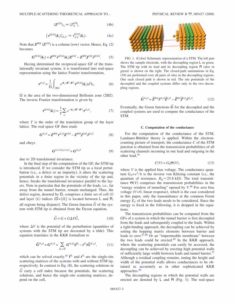
An important approximation in the proposed method isthat the conductance is computed in a finite-sized cluster Caround the STM tip �Eq. �19� and Sec. II D�. The method hasto be rendered unusable if the conductance does not con-verge with increasing number of cells within the layers.Therefore, the convergence of the transmittance has to bechecked by increasing the lateral size of the real-space clus-ter C.
Two energies are considered. The first, 0.2 eV below theFermi level �EF�, is within the energy range covered by the Lgap surface state present at the bare Au�111� surface. Notethat this surface state has a band minimum at EF−0.5 eV andshows parabolic dispersion.84 The other energy, 1.0 eV be-low EF, accounts only for Au bulk states. For both energies,the transmittance �� �Eq. �22�� plotted versus number ofcells within a layer of the tunnel junction starts to increasealmost linearly and saturates at about 190 cells per layer�Fig. 3�. In order to find the converged values ��� of ��,the curves are fitted to ���x�=���−a exp�−bx� �red in Fig.3�, where x is the number of cells per layer. From the fits weobtain ���=0.000 543 and 0.000 173 for EF−0.2 eV andEF−1.0 eV, respectively �indicated by green asterisks�. Ourfinding corresponds nicely to the trend observed in Ref. 54.
The trend can be understood by considering the cone-shaped flux through the STM tip as follows. Areas far apartfrom the STM tip can be regarded as planar tunnel junctions,
the electrodes of which are separated by four vacuum layers.In contrast, the tip-sample separation at the apex atom of theSTM tip is only two layers. Hence, the contribution of thearea around the STM tip to the conductance is much largerthan that of the remainder of the system �although its area ismuch larger�. That can be understood by the exponential de-crease of the transmittance through a tunnel barrier with in-creasing electrode separation. Due to scattering at the tipatoms, the current flows in a cone with moderate openingangle, the cone being centered about the apex atom of the tip.�A similar behavior is found in quantum point contacts.55�For a converged conductance, the summation over the cellsin L and R �Eq. �19�� has to cover at least the cross section ofthe cone.
B. Effect of the STM tip on the sample
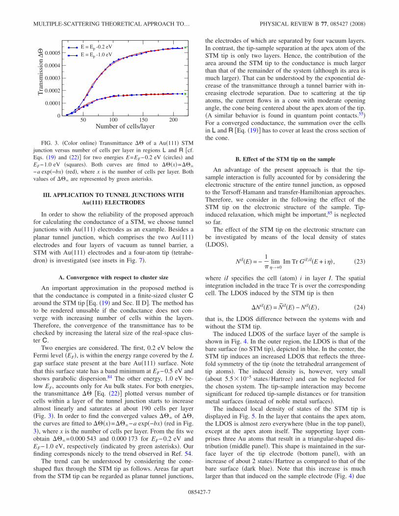
An advantage of the present approach is that the tip-sample interaction is fully accounted for by considering theelectronic structure of the entire tunnel junction, as opposedto the Tersoff-Hamann and transfer-Hamiltonian approaches.Therefore, we consider in the following the effect of theSTM tip on the electronic structure of the sample. Tip-induced relaxation, which might be important,85 is neglectedso far.
The effect of the STM tip on the electronic structure canbe investigated by means of the local density of states�LDOS�,
NiI�E� = −1
�lim
�→+0Im Tr GiI;iI�E + i�� , �23�
where iI specifies the cell �atom� i in layer I. The spatialintegration included in the trace Tr is over the correspondingcell. The LDOS induced by the STM tip is then
�NiI�E� = NiI�E� − NiI�E� , �24�
that is, the LDOS difference between the systems with andwithout the STM tip.
The induced LDOS of the surface layer of the sample isshown in Fig. 4. In the outer region, the LDOS is that of thebare surface �no STM tip�, depicted in blue. In the center, theSTM tip induces an increased LDOS that reflects the three-fold symmetry of the tip �note the tetrahedral arrangement oftip atoms�. The induced density is, however, very small�about 5.5 10−5 states /Hartree� and can be neglected forthe chosen system. The tip-sample interaction may becomesignificant for reduced tip-sample distances or for transitionmetal surfaces �instead of noble metal surfaces�.
The induced local density of states of the STM tip isdisplayed in Fig. 5. In the layer that contains the apex atom,the LDOS is almost zero everywhere �blue in the top panel�,except at the apex atom itself. The supporting layer com-prises three Au atoms that result in a triangular-shaped dis-tribution �middle panel�. This shape is maintained in the sur-face layer of the tip electrode �bottom panel�, with anincrease of about 2 states /Hartree as compared to that of thebare surface �dark blue�. Note that this increase is muchlarger than that induced on the sample electrode �Fig. 4� due
50 100 150 200Number of cells/layer
0
0.0001
0.0002
0.0003
0.0004
0.0005
Tra
nsm
issi
onE = E
F-0.2 eV
E = EF
-1.0 eV∆Θ
FIG. 3. �Color online� Transmittance �� of a Au�111� STMjunction versus number of cells per layer in regions L and R �cf.Eqs. �19� and �22�� for two energies E=EF−0.2 eV �circles� andEF−1.0 eV �squares�. Both curves are fitted to ���x�=���
−a exp�−bx� �red�, where x is the number of cells per layer. Bothvalues of ��� are represented by green asterisks.
MULTIPLE-SCATTERING THEORETICAL APPROACH TO… PHYSICAL REVIEW B 77, 085427 �2008�
085427-7
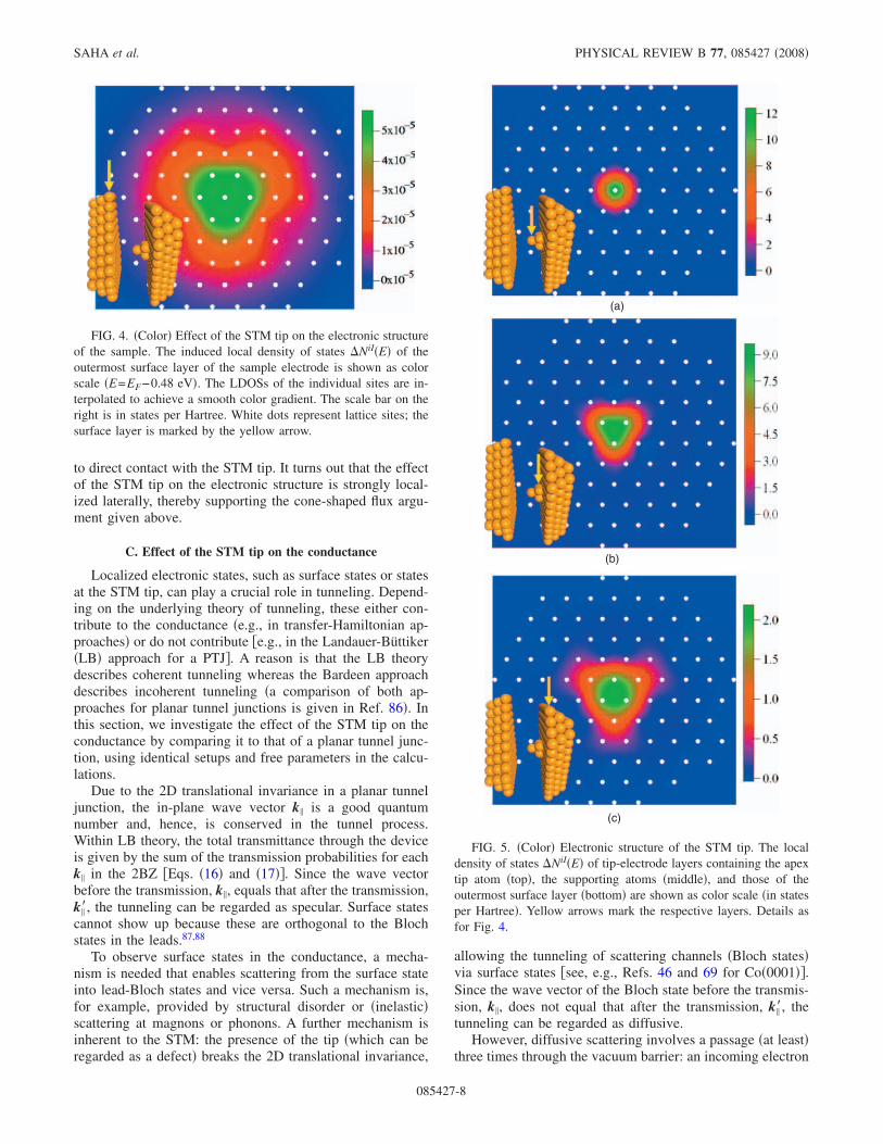
to direct contact with the STM tip. It turns out that the effectof the STM tip on the electronic structure is strongly local-ized laterally, thereby supporting the cone-shaped flux argu-ment given above.
C. Effect of the STM tip on the conductance
Localized electronic states, such as surface states or statesat the STM tip, can play a crucial role in tunneling. Depend-ing on the underlying theory of tunneling, these either con-tribute to the conductance �e.g., in transfer-Hamiltonian ap-proaches� or do not contribute �e.g., in the Landauer-Büttiker�LB� approach for a PTJ�. A reason is that the LB theorydescribes coherent tunneling whereas the Bardeen approachdescribes incoherent tunneling �a comparison of both ap-proaches for planar tunnel junctions is given in Ref. 86�. Inthis section, we investigate the effect of the STM tip on theconductance by comparing it to that of a planar tunnel junc-tion, using identical setups and free parameters in the calcu-lations.
Due to the 2D translational invariance in a planar tunneljunction, the in-plane wave vector k� is a good quantumnumber and, hence, is conserved in the tunnel process.Within LB theory, the total transmittance through the deviceis given by the sum of the transmission probabilities for eachk� in the 2BZ �Eqs. �16� and �17��. Since the wave vectorbefore the transmission, k�, equals that after the transmission,k��, the tunneling can be regarded as specular. Surface statescannot show up because these are orthogonal to the Blochstates in the leads.87,88
To observe surface states in the conductance, a mecha-nism is needed that enables scattering from the surface stateinto lead-Bloch states and vice versa. Such a mechanism is,for example, provided by structural disorder or �inelastic�scattering at magnons or phonons. A further mechanism isinherent to the STM: the presence of the tip �which can beregarded as a defect� breaks the 2D translational invariance,
allowing the tunneling of scattering channels �Bloch states�via surface states �see, e.g., Refs. 46 and 69 for Co�0001��.Since the wave vector of the Bloch state before the transmis-sion, k�, does not equal that after the transmission, k��, thetunneling can be regarded as diffusive.
However, diffusive scattering involves a passage �at least�three times through the vacuum barrier: an incoming electron
FIG. 4. �Color� Effect of the STM tip on the electronic structureof the sample. The induced local density of states �NiI�E� of theoutermost surface layer of the sample electrode is shown as colorscale �E=EF−0.48 eV�. The LDOSs of the individual sites are in-terpolated to achieve a smooth color gradient. The scale bar on theright is in states per Hartree. White dots represent lattice sites; thesurface layer is marked by the yellow arrow.
(a)
(b)
(c)
FIG. 5. �Color� Electronic structure of the STM tip. The localdensity of states �NiI�E� of tip-electrode layers containing the apextip atom �top�, the supporting atoms �middle�, and those of theoutermost surface layer �bottom� are shown as color scale �in statesper Hartree�. Yellow arrows mark the respective layers. Details asfor Fig. 4.
SAHA et al. PHYSICAL REVIEW B 77, 085427 �2008�
085427-8
is scattered at the tip, propagates through the barrier into thesurface states, and propagates back to the tip, where it isscattered into an outgoing Bloch state which has to pass thebarrier again to become outgoing in the other electrode. Con-sequently, surface states do not show up in the conductancefor large tip-sample distances but can contribute significantlyfor small separations �note the exponential decrease of thetransmittance with increasing electrode separation�. Withinthis respect, we expect a very weak effect of the L gap sur-face state on the conductance, as is also suggested by theweak tip-sample interaction �Fig. 4�. A more important effectis expected from electronic states located at the tip �Fig. 5�.Here, the passage of an electron through the barrier takesplace at least once and, hence, the contribution of tip states tothe conductance is expected to be much larger than that ofthe surface states.
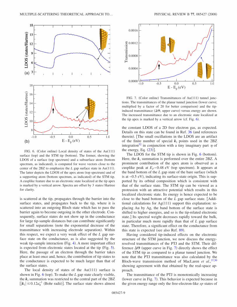
The local density of states of the Au�111� surface isshown in Fig. 6 �top�. To make the L gap state clearly visible,the k� summation was restricted to the central part of the 2BZ�k� �0.12a0
−1 �Bohr radii��. The surface state shows almost
the constant LDOS of a 2D free electron gas, as expected.Details on this state can be found in Ref. 36 �and referencestherein�. �The small oscillations in the LDOS are an artifactof the finite number of special k� points used in the 2BZintegration52 in conjunction with a tiny imaginary part � ofthe energy, Eq. �23��.
The LDOS for the STM tip is shown in Fig. 6 �bottom�.Here, the k� summation is performed over the entire 2BZ. Aprominent contribution of the apex atom is observed as acusplike peak at EF−0.48 eV �top spectrum�. It appears atthe band bottom of the L gap state of the bare surface �whichis at −0.5 eV�, indicating its surface-state origin. This is sup-ported by its orbital composition which is consistent withthat of the surface state. The STM tip can be viewed as aprotrusion with an attractive potential which results in thislocalized electronic state. Its energy is hence expected to beclose to the band bottom of the L gap surface state. �Addi-tional calculations for Ag�111� support this explanation: re-placing Au by Ag, the band bottom of the surface state isshifted to higher energies, and so is the tip-related electronicstate.� Its spectral weight decreases rapidly toward the bulk,in particular much more rapidly than that of L gap surfacestate. Therefore, a significant effect on the conductance fromthis state is expected �see also Ref. 89�.
Having considered tip-induced effects on the electronicstructure of the STM junction, we now discuss the energy-resolved transmittances of the PTJ and the STM. Their dif-ference �� �upper curve in Fig. 7� directly shows the effectof the STM tip as compared to a planar tunnel junction. Wenote that the PTJ transmittance was also calculated by theBloch-wave transmission method of MacLaren et al.,37,50
showing agreement with that obtained by the real-space ap-proach.
The transmittance of the PTJ is monotonically increasing�lower curve in Fig. 7�. This behavior is expected because inthe given energy range only the free-electron-like sp states of
(a)
8
10
12
14
16
18
LD
OS
(sta
tes/
Har
tree
)
-1.0 -0.5 0.0 0.5 1.0E - E
F(eV)(b)
FIG. 6. �Color online� Local density of states of the Au�111�surface �top� and the STM tip �bottom�. The former, showing theLDOS of a surface �top spectrum� and a subsurface atom �bottomspectrum, as indicated�, is computed for wave vectors close to thecenter of the 2BZ to emphasize the L gap surface state in Au�111�.The latter depicts the LDOS of the apex atom �top spectrum� and ofa supporting atom �bottom spectrum, as indicated� of the STM tip.A cusplike feature due to an electronic state localized at the tip apexis marked by a vertical arrow. Spectra are offset by 3 states /Hartreefor clarity.
-1.0 -0.5 0.0 0.5 1.0E - E
F(eV)
0.0000
0.0004
0.0008
0.0012
0.0016
Tra
nsm
issi
on
FIG. 7. �Color online� Transmittances of Au�111� tunnel junc-tions. The transmittances of the planar tunnel junction �lower curve;multiplied by a factor of 20 for better comparison� and the tip-induced transmittance ���, upper curve� versus energy are shown.The increased transmittance due to an electronic state localized atthe tip apex is marked by a vertical arrow �cf. Fig. 6�.
MULTIPLE-SCATTERING THEORETICAL APPROACH TO… PHYSICAL REVIEW B 77, 085427 �2008�
085427-9
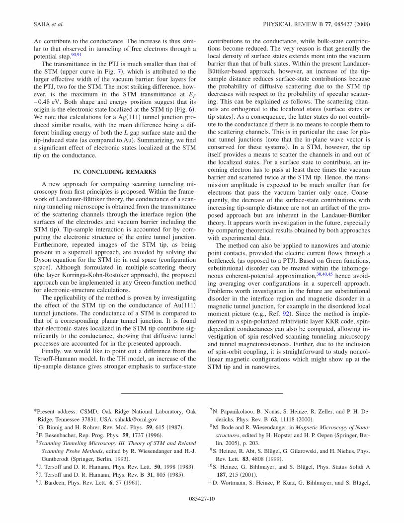
Au contribute to the conductance. The increase is thus simi-lar to that observed in tunneling of free electrons through apotential step.90,91
The transmittance in the PTJ is much smaller than that ofthe STM �upper curve in Fig. 7�, which is attributed to thelarger effective width of the vacuum barrier: four layers forthe PTJ, two for the STM. The most striking difference, how-ever, is the maximum in the STM transmittance at EF−0.48 eV. Both shape and energy position suggest that itsorigin is the electronic state localized at the STM tip �Fig. 6�.We note that calculations for a Ag�111� tunnel junction pro-duced similar results, with the main difference being a dif-ferent binding energy of both the L gap surface state and thetip-induced state �as compared to Au�. Summarizing, we finda significant effect of electronic states localized at the STMtip on the conductance.
IV. CONCLUDING REMARKS
A new approach for computing scanning tunneling mi-croscopy from first principles is proposed. Within the frame-work of Landauer-Büttiker theory, the conductance of a scan-ning tunneling microscope is obtained from the transmittanceof the scattering channels through the interface region �thesurfaces of the electrodes and vacuum barrier including theSTM tip�. Tip-sample interaction is accounted for by com-puting the electronic structure of the entire tunnel junction.Furthermore, repeated images of the STM tip, as beingpresent in a supercell approach, are avoided by solving theDyson equation for the STM tip in real space �configurationspace�. Although formulated in multiple-scattering theory�the layer Korringa-Kohn-Rostoker approach�, the proposedapproach can be implemented in any Green-function methodfor electronic-structure calculations.
The applicability of the method is proven by investigatingthe effect of the STM tip on the conductance of Au�111�tunnel junctions. The conductance of a STM is compared tothat of a corresponding planar tunnel junction. It is foundthat electronic states localized in the STM tip contribute sig-nificantly to the conductance, showing that diffusive tunnelprocesses are accounted for in the presented approach.
Finally, we would like to point out a difference from theTersoff-Hamann model. In the TH model, an increase of thetip-sample distance gives stronger emphasis to surface-state
contributions to the conductance, while bulk-state contribu-tions become reduced. The very reason is that generally thelocal density of surface states extends more into the vacuumbarrier than that of bulk states. Within the present Landauer-Büttiker-based approach, however, an increase of the tip-sample distance reduces surface-state contributions becausethe probability of diffusive scattering due to the STM tipdecreases with respect to the probability of specular scatter-ing. This can be explained as follows. The scattering chan-nels are orthogonal to the localized states �surface states ortip states�. As a consequence, the latter states do not contrib-ute to the conductance if there is no means to couple them tothe scattering channels. This is in particular the case for pla-nar tunnel junctions �note that the in-plane wave vector isconserved for these systems�. In a STM, however, the tipitself provides a means to scatter the channels in and out ofthe localized states. For a surface state to contribute, an in-coming electron has to pass at least three times the vacuumbarrier and scattered twice at the STM tip. Hence, the trans-mission amplitude is expected to be much smaller than forelectrons that pass the vacuum barrier only once. Conse-quently, the decrease of the surface-state contributions withincreasing tip-sample distance are not an artifact of the pro-posed approach but are inherent in the Landauer-Büttikertheory. It appears worth investigation in the future, especiallyby comparing theoretical results obtained by both approacheswith experimental data.
The method can also be applied to nanowires and atomicpoint contacts, provided the electric current flows through abottleneck �as opposed to a PTJ�. Based on Green functions,substitutional disorder can be treated within the inhomoge-neous coherent-potential approximation,30,40,45 hence avoid-ing averaging over configurations in a supercell approach.Problems worth investigation in the future are substitutionaldisorder in the interface region and magnetic disorder in amagnetic tunnel junction, for example in the disordered localmoment picture �e.g., Ref. 92�. Since the method is imple-mented in a spin-polarized relativistic layer KKR code, spin-dependent conductances can also be computed, allowing in-vestigation of spin-resolved scanning tunneling microscopyand tunnel magnetoresistances. Further, due to the inclusionof spin-orbit coupling, it is straightforward to study noncol-linear magnetic configurations which might show up at theSTM tip and in nanowires.
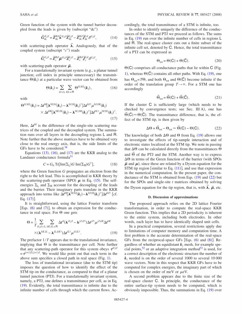
*Present address: CSMD, Oak Ridge National Laboratory, OakRidge, Tennessee 37831, USA. [email protected]
1 G. Binnig and H. Rohrer, Rev. Mod. Phys. 59, 615 �1987�.2 F. Besenbacher, Rep. Prog. Phys. 59, 1737 �1996�.3 Scanning Tunneling Microscopy III. Theory of STM and Related
Scanning Probe Methods, edited by R. Wiesendanger and H.-J.Güntherodt �Springer, Berlin, 1993�.
4 J. Tersoff and D. R. Hamann, Phys. Rev. Lett. 50, 1998 �1983�.5 J. Tersoff and D. R. Hamann, Phys. Rev. B 31, 805 �1985�.6 J. Bardeen, Phys. Rev. Lett. 6, 57 �1961�.
7 N. Papanikolaou, B. Nonas, S. Heinze, R. Zeller, and P. H. De-derichs, Phys. Rev. B 62, 11118 �2000�.
8 M. Bode and R. Wiesendanger, in Magnetic Microscopy of Nano-structures, edited by H. Hopster and H. P. Oepen �Springer, Ber-lin, 2005�, p. 203.
9 S. Heinze, R. Abt, S. Blügel, G. Gilarowski, and H. Niehus, Phys.Rev. Lett. 83, 4808 �1999�.
10 S. Heinze, G. Bihlmayer, and S. Blügel, Phys. Status Solidi A187, 215 �2001�.
11 D. Wortmann, S. Heinze, P. Kurz, G. Bihlmayer, and S. Blügel,
SAHA et al. PHYSICAL REVIEW B 77, 085427 �2008�
085427-10
Phys. Rev. Lett. 86, 4132 �2001�.12 M. Bode, S. Heinze, A. Kubetzka, O. Pietzsch, X. Nie, G. Bihl-
mayer, S. Blügel, and R. Wiesendanger, Phys. Rev. Lett. 89,237205 �2002�.
13 M. Bode, A. Kubetzka, S. Heinze, O. Pietzsch, R. Wiesendanger,M. Heide, X. Nie, G. Bihlmayer, and S. Blügel, J. Phys.: Con-dens. Matter 15, S679 �2003�.
14 K. von Bergmann, M. Bode, A. Kubetzka, M. Heide, S. Blügel,and R. Wiesendanger, Phys. Rev. Lett. 92, 046801 �2004�.
15 W. A. Hofer and J. Redinger, Philos. Mag. B 78, 519 �1998�.16 W. A. Hofer, Prog. Surf. Sci. 71, 147 �2003�.17 W. A. Hofer, J. Redinger, A. Biedermann, and P. Varga, Surf. Sci.
482-485, 1113 �2001�.18 Y. Imry and R. Landauer, Rev. Mod. Phys. 71, S306 �1999�.19 K. S. Thygesen and K. W. Jacobsen, Phys. Rev. B 72, 033401
�2005�.20 J. M. Blanco, C. González, P. Jelínek, J. Ortega, F. Flores, and R.
Pérez, Phys. Rev. B 70, 085405 �2004�.21 W. H. Butler, Phys. Rev. B 31, 3260 �1985�.22 P. Weinberger, P. Levy, J. Banhart, L. Szunyogh, and B. Új-
falussy, J. Phys.: Condens. Matter 8, 7677 �1996�.23 K. Carva, I. Turek, J. Kudrnovský, and O. Bengone, Phys. Rev. B
73, 144421 �2006�.24 R. Zeller, Phys. Rev. B 55, 9400 �1997�.25 R. Zeller, P. H. Dederichs, B. Újfalussy, L. Szunyogh, and P.
Weinberger, Phys. Rev. B 52, 8807 �1995�.26 K. Wildberger, R. Zeller, and P. H. Dederichs, Phys. Rev. B 55,
10074 �1997�.27 J. Schwitalla and B. L. Györffy, J. Phys.: Condens. Matter 10,
10995 �1998�.28 N. Y. Moghadam, G. M. Stocks, B. Újfalussy, W. A. Shelton, A.
Gonis, and J. S. Faulkner, J. Phys.: Condens. Matter 11, 5505�1999�.
29 I. Turek, J. Kudrnovský, V. Drchal, L. Szunyogh, and P. Wein-berger, Phys. Rev. B 65, 125101 �2002�.
30 Electron Scattering in Solid Matter, edited by J. Zabloudil, R.Hammerling, L. Szunyogh, and P. Weinberger �Springer, Berlin,2005�.
31 C. Uiberacker, J. Zabloudil, P. Weinberger, L. Szunyogh, and C.Sommers, Phys. Rev. Lett. 82, 1289 �1999�.
32 J. Henk, A. M. N. Niklasson, and B. Johansson, Phys. Rev. B 59,9332 �1999�.
33 G. Nicolay, F. Reinert, S. Hüfner, and P. Blaha, Phys. Rev. B 65,033407 �2001�.
34 J. Henk, A. Ernst, and P. Bruno, Phys. Rev. B 68, 165416 �2003�.35 F. Reinert, J. Phys.: Condens. Matter 15, S693 �2003�.36 J. Henk, M. Hoesch, J. Osterwalder, A. Ernst, and P. Bruno, J.
Phys.: Condens. Matter 16, 7581 �2004�.37 J. Henk, A. Ernst, K. K. Saha, and P. Bruno, J. Phys.: Condens.
Matter 18, 2601 �2006�.38 P. Weinberger, Electron Scattering Theory of Ordered and Disor-
dered Matter �Clarendon Press, Oxford, 1990�.39 I. Mertig, E. Mrosan, and P. Ziesche, Multiple Scattering Theory
of Point Defects in Metals: Electronic Properties �B. G. Teub-ner, Leipzig, 1987�.
40 A. Gonis, Green Functions for Ordered and Disordered Systems,Studies in Mathematical Physics, Vol. 4 �North-Holland, Am-sterdam, 1992�.
41 J. Henk, in Handbook of Thin Film Materials, edited by H. S.Nalwa �Academic Press, San Diego, 2001�, Vol. 2, Chap. 10, p.
479.42 E. M. Rose, Relativistic Electron Theory �Wiley & Sons, New
York, 1961�.43 P. Strange, Relativistic Quantum Mechanics: With Applications in
Condensed Matter and Atomic Physics �Cambridge UniversityPress, Cambridge, U.K., 1998�.
44 E. Tamura, Phys. Rev. B 45, 3271 �1992�.45 J. S. Faulkner and G. M. Stocks, Phys. Rev. B 21, 3222 �1980�.46 J. Henk and P. Bruno, Phys. Rev. B 68, 174430 �2003�.47 J. Mathon and A. Umerski, Phys. Rev. B 60, 1117 �1999�.48 J. Mathon and A. Umerski, Phys. Rev. B 63, 220403�R� �2001�.49 J. B. Pendry, A. B. Prête, and B. C. H. Krutzen, J. Phys.: Con-
dens. Matter 3, 4313 �1991�.50 J. M. MacLaren, X.-G. Zhang, W. H. Butler, and X. Wang, Phys.
Rev. B 59, 5470 �1999�.51 D. S. Fisher and P. A. Lee, Phys. Rev. B 23, 6851 �1981�.52 R. Evarestov and V. Smirnow, Phys. Status Solidi B 119, 9
�1983�.53 J. Henk, Phys. Rev. B 64, 035412 �2001�.54 K. Palotás, B. Lazarovits, L. Szunyogh, and P. Weinberger, Phys.
Rev. B 70, 134421 �2004�.55 G. Metalidis and P. Bruno, Phys. Rev. B 72, 235304 �2005�.56 N. D. Lang, Phys. Rev. Lett. 56, 1164 �1986�.57 N. D. Lang, Phys. Rev. B 34, 5947 �1986�.58 N. D. Lang, Phys. Rev. B 36, 8173 �1987�.59 Y. Y. Sharvin, Sov. Phys. JETP 21, 655 �1965�.60 K. Palotás, B. Lazarovits, L. Szunyogh, and P. Weinberger, Phys.
Rev. B 67, 174404 �2003�.61 V. Popescu, H. Ebert, N. Papanikolaou, R. Zeller, and P. H. De-
derichs, J. Phys.: Condens. Matter 16, S5579 �2004�.62 P. Mavropoulos, N. Papanikolaou, and P. H. Dederichs, Phys.
Rev. B 69, 125104 �2004�.63 C. Tusche, H. L. Meyerheim, N. Jedrecy, G. Renaud, A. Ernst, J.
Henk, P. Bruno, and J. Kirschner, Phys. Rev. Lett. 95, 176101�2005�.
64 A. Gonis, A. J. Freeman, and P. Weinberger, Phys. Rev. B 32,7713 �1985�.
65 N. Stefanou, P. J. Braspenning, R. Zeller, and P. H. Dederichs,Phys. Rev. B 36, 6372 �1987�.
66 L. Olesen, M. Brandbyge, M. R. Sørensen, K. W. Jacobsen, E.Lægsgaard, I. Stensgaard, and F. Besenbacher, Phys. Rev. Lett.76, 1485 �1996�.
67 R. Z. Huang, V. S. Stepanyuk, A. L. Klavsyuk, W. Hergert, P.Bruno, and J. Kirschner, Phys. Rev. B 73, 153404 �2006�.
68 M. Brandbyge, J.-L. Mozos, P. Ordejon, J. Taylor, and K. Stok-bro, Phys. Rev. B 65, 165401 �2002�.
69 H. F. Ding, W. Wulfhekel, J. Henk, P. Bruno, and J. Kirschner,Phys. Rev. Lett. 90, 116603 �2003�.
70 N. D. Lang, Phys. Rev. B 37, 10395 �1988�.71 J. M. Pitarke, P. M. Echenique, and F. Flores, Surf. Sci. 217, 267
�1989�.72 K. Palotás and W. A. Hofer, J. Phys.: Condens. Matter 17, 2705
�2005�.73 W. A. Hofer and A. Garcia-Lekue, Phys. Rev. B 71, 085401
�2005�.74 M. Woods, A. Ernst, P. Strange, and W. M. Temmerman, J. Phys.:
Condens. Matter 13, 8607 �2001�.75 M. Lüders, A. Ernst, W. M. Temmerman, Z. Szotek, and P. J.
Durham, J. Phys.: Condens. Matter 13, 8587 �2001�.76 A. Ernst, J. Henk, and R. K. Thapa, J. Phys.: Condens. Matter 17,
MULTIPLE-SCATTERING THEORETICAL APPROACH TO… PHYSICAL REVIEW B 77, 085427 �2008�
085427-11

3269 �2005�.77 M. Lüders, A. Ernst, M. Däne, Z. Szotek, A. Svane, D. Ködder-
itzsch, W. Hergert, B. L. Györffy, and W. M. Temmerman, Phys.Rev. B 71, 205109 �2005�.
78 X.-G. Zhang and D. M. C. Nicholson, Phys. Rev. B 60, 4551�1999�.
79 D. M. Heyes and F. van Swol, J. Chem. Phys. 75, 5051 �1981�.80 J. M. Blanco, F. Flores, and R. Pérez, Prog. Surf. Sci. 81, 403
�2006�.81 C. R. Ast, J. Henk, A. Ernst, L. Moreschini, M. C. Falub, D.
Pacilé, P. Bruno, K. Kern, and M. Grioni, Phys. Rev. Lett. 98,186807 �2007�.
82 A. L. Vázquez de Parga, O. S. Hernán, R. Miranda, A. LevyYeyati, N. Mingo, A. Martin-Rodero, and F. Flores, Phys. Rev.Lett. 80, 357 �1998�.
83 F. Reinert and G. Nicolay, Appl. Phys. A: Mater. Sci. Process. 78,817 �2004�.
84 S. LaShell, B. A. McDougall, and E. Jensen, Phys. Rev. Lett. 77,3419 �1996�.
85 R. Z. Huang, V. S. Stepanyuk, and J. Kirschner, J. Phys.: Con-dens. Matter 18, L217 �2006�.
86 D. Wortmann, H. Ishida, and S. Blügel, Phys. Rev. B 72, 235113�2005�.
87 P. M. Levy, K. Wang, P. H. Dederichs, C. Heide, S. Zhang, and L.Szunyogh, Philos. Mag. B 82, 763 �2002�.
88 H. Ishida, D. Wortmann, and T. Ohwaki, Phys. Rev. B 70,085409 �2004�.
89 R. M. Tromp, E. J. van Loenen, J. E. Demuth, and N. D. Lang,Phys. Rev. B 37, 9042 �1988�.
90 E. Merzbacher, Quantum Mechanics, 2nd ed. �John Wiley &Sons, New York, 1970�.
91 J. C. Slonczewski, Phys. Rev. B 39, 6995 �1989�.92 J. Staunton, B. L. Gyorffy, A. J. Pindor, G. M. Stocks, and H.
Winter, J. Magn. Magn. Mater. 45, 15 �1984�.
SAHA et al. PHYSICAL REVIEW B 77, 085427 �2008�
085427-12