multiband analog and digital television tuner max3543 - maxim
TRANSCRIPT
_______________________________________________________________ Maxim Integrated Products 1
For pricing, delivery, and ordering information, please contact Maxim Direct at 1-888-629-4642, or visit Maxim’s website at www.maxim-ic.com.
Multiband Analog andDigital Television Tuner M
AX
35
43
19-4985; Rev 2; 7/10
Ordering Information
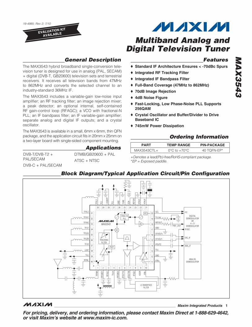
Block Diagram/Typical Application Circuit/Pin Configuration
General DescriptionThe MAX3543 hybrid broadband single-conversion tele-vision tuner is designed for use in analog (PAL, SECAM) + digital (DVB-T, GB20600) television sets and terrestrial receivers. It receives all television bands from 47MHz to 862MHz and converts the selected channel to an industry-standard 36MHz IF.
The MAX3543 includes a variable-gain low-noise input amplifier; an RF tracking filter; an image rejection mixer; a peak detector; an optional internal, self-contained RF gain-control loop (RFAGC); a VCO with fractional-N PLL; an IF bandpass filter; an IF variable-gain amplifier; separate analog and digital IF outputs; and a crystal oscillator.
The MAX3543 is available in a small, 6mm x 6mm, thin QFN package, and the application circuit fits in 20mm x 25mm on a two-layer board with single-sided component mounting.
Applications
FeaturesS Standard IF Architecture Ensures < -70dBc Spurs
S Integrated RF Tracking Filter
S Integrated IF Bandpass Filter
S Full-Band Coverage (47MHz to 862MHz)
S 70dB Image Rejection
S 4dB Noise Figure
S Fast-Locking, Low Phase-Noise PLL Supports 256QAM
S Crystal Oscillator and Buffer/Divider to Drive Baseband IC
S 745mW Power Dissipation
+Denotes a lead(Pb)-free/RoHS-compliant package.*EP = Exposed paddle.
DVB-T/DVB-T2 + PAL/SECAM
DVB-C + PAL/SECAM
DTMB/GB20600 + PAL
ATSC + NTSC
EVALUATION KIT
AVAILABLE
PART TEMP RANGE PIN-PACKAGE
MAX3543CTL+ 0NC to +70NC 40 TQFN-EP*
+
35
36
34
33
12
11
13
RFGN
D1
V CCI
F
RFGN
D2
IFOU
T1A
IFOU
T1B
14
RFIN
H
V CC
TUNE
SDA
LDOB
YP
V CC
TFVL
1
REFD
IV
XTAL
E
1 2
TFU1
4 5 6 7
27282930 26 24 23 22
TFU2A
TFU2B
REFOUT
GND
DTVOUT+
DTVOUT-
RFVG
C
GND
3
25
37TFU3 IFOUT2
38
39
40
LEXT
VCC
RFINL
VCC
GND
IFIN+
TFVH2
32
15
VCCDIGTFVH1
31
16
17
18
19
20SCL
IFVG
C
ADDR
IFIN
-XT
ALB
8 9 10
21
TFVL2
MAX3543
I2C I2C
IFVGC
REF_OUT
DIGITALDEMODULATOR
ORA + D
DEMODULATOR
ANALOGDEMODULATOR
LC BANDPASSFILTER
DIG_IF
ANA_IF
FRAC-NPLL
/N
TRACKINGFILTER
PDET
NOTE: LAYOUT FITS 25mm x 20mm ON 2-LAYER BOARD WITH DEVICE PLACEMENT ON TOP SIDE ONLY.
Multiband Analog andDigital Television Tuner
MA
X3
54
3
2 ______________________________________________________________________________________
Stresses beyond those listed under “Absolute Maximum Ratings” may cause permanent damage to the device. These are stress ratings only, and functional operation of the device at these or any other conditions beyond those indicated in the operational sections of the specifications is not implied. Exposure to absolute maximum rating conditions for extended periods may affect device reliability.
VCC to GND ..........................................................-0.3V to +3.6VRFINL, RFINH, IFIN+, IFIN-, DTVOUT+, DTVOUT-,
IFOUT1A, IFOUT1B, IFOUT2 ............... -0.3V to (VCC + 0.3V)SDA, SCLK, IFAGC, RFVGA ................................-0.3V to +3.6VShort-Circuit Protection: DTVOUT+, DTVOUT-,
IFOUT1A, IFOUT1B, IFOUT2 .................................... IndefiniteRF Input Power ..............................................................+10dBm
Continuous Power Dissipation (TA = +70NC)(derate 35.7mW/NC above +70NC) ............................2857mW
Operating Temperature Range ............................. 0NC to +70NCJunction Temperature .....................................................+150NCStorage Temperature Range ............................ -65NC to +165NCLead Temperature (soldering, 10s) ................................+300NCSoldering Temperature (reflow) ......................................+260NC
DC ELECTRICAL CHARACTERISTICS(MAX3543 Evaluation Kit, VCC = 3.1V to 3.5V, TA = 0NC to +70NC, registers set according to Table 1. Typical values are at VCC = 3.3V, TA = +25NC, unless otherwise noted.) (Note 1)
ABSOLUTE MAXIMUM RATINGS
AC ELECTRICAL CHARACTERISTICS(MAX3543 Evaluation Kit, RF center frequency = 666MHz, IF center frequency = 36.15MHz, registers set according to Table 1, fREF = 16MHz, VRFVGC = VIFVGC = 3.0V, VCC = 3.3V, TA = +25NC, unless otherwise noted.)
PARAMETER CONDITIONS MIN TYP MAX UNITS
SUPPLY VOLTAGE AND CURRENT
Supply Voltage 3.1 3.5 V
Supply CurrentIF VGA enabled 225 270
mAStandby (REF oscillator on) R08[7] = 1 5
RF and IF VGC InputBias Current
At 0.5V to 3.0V DC-100 to +100
FA
RF and IF VGC Control Voltage Maximum gain 3.0 V
RF and IF VGC Control Voltage Minimum gain 0.5 V
SERIAL INTERFACE
Input Logic-Level Low0.3 x VCC
V
Input Logic-Level High0.7 x VCC
V
Output Logic-Level Low 3mA sink current 0.4 V
Output Logic-Level HighVCC - 0.5V
V
Maximum Clock Rate 400 kHz
PARAMETER CONDITIONS MIN TYP MAX UNITS
OVERALL REQUIREMENTS (RF INPUT TO IF OUTPUT)
RFINL OperatingFrequency Range
Tunable frequency range 47 345 MHz
RFINH OperatingFrequency Range
Tunable frequency range 345 862 MHz
Maximum VoltageGain to IFOUT1
DVB-T mode (see Table 1) 50 dB

Multiband Analog andDigital Television Tuner
MA
X3
54
3
_______________________________________________________________________________________ 3
AC ELECTRICAL CHARACTERISTICS (continued)(MAX3543 Evaluation Kit, RF center frequency = 666MHz, IF center frequency = 36.15MHz, registers set according to Table 1, fREF = 16MHz, VRFVGC = VIFVGC = 3.0V, VCC = 3.3V, TA = +25NC, unless otherwise noted.)
Note 1: Guaranteed by production test at +25NC. 0NC and +70NC are guaranteed by design and characterization.Note 2: Guaranteed by design and characterization.
PARAMETER CONDITIONS MIN TYP MAX UNITS
RF Gain Control Range (gain at VRFVGC = 3.0V) - (gain at VRFVGC = 0.5V) 53 dB
Noise Figure 4 dB
Image RejectionImage applied at 77.8MHzabove desired channel’scenter frequency
47MHz to 470MHz > 70dB
470MHz to 862MHz > 65
IF VARIABLE-GAIN AMPLIFIER
Maximum Voltage Gain Output load impedance > 2kI||3pF, differential load 60 dB
Minimum Voltage GainOutput load impedance > 2kI||3pF, differential load, VIFVGC = 0.5V
19 dB
In-Channel Output V1dB 36.15MHz CW output signal > 2.5 VP-P
DETECTOR
Wideband DetectorInput-Referred Attack Point
Programmable, R0B[6:4] = 100, CW input signal -36 dBm
Narrowband DetectorInput-Referred Attack Point
Programmable, R0B[2:0] = 011, CW input signal -47 dBm
SIGMA-DELTA FRAC-N SYNTHESIZER
N-Divider Value 19 251
Fractional-N Resolution 20 Bits
Phase-Detector Frequency fXTAL/2 8 10.5 MHz
Phase-Detector Frequency fXTAL/1 16 21 MHz
REFERENCE OSCILLATOR
Frequency (Note 2) 16 32 MHz
External Overdrive Level AC-coupled sine-wave input 0.5 1.5 VP-P
REFERENCE OSCILLATOR OUTPUT BUFFER
Output Frequency /1, /4 modes 4 4 fXTAL MHz
Output Level Load Impedance > 20kI||3pF 1.1 VP-P

Multiband Analog andDigital Television Tuner
MA
X3
54
3
4 ______________________________________________________________________________________
Typical Register SummaryTable 1 shows register settings to configure the MAX3543 for operation with a 16MHz crystal frequency and 666MHz RF frequency with a differential LC bandpass filter.
Table 1. Typical Register Settings
REGISTER NAME
REGISTER ADDRESS
REGISTER FUNCTIONDVB-T MODE, 8MHz
DIFFERENTIAL IF(hex)
PAL MODE,ATV OUTPUT
(hex)
R00 0x00 VCO 4C 4C
R01 0x01 NDIV INT 2B 57
R02 0x02 NDIV FRAC2 8E 9C
R03 0x03 NDIV FRAC1 26 4C
R04 0x04 NDIV FRAC0 (VAS Trigger) 66 CD
R05 0x05 MODE CTRL D8 DA
R06 0x06 TFS Calculated from ROM values Calculated from ROM values
R07 0x07 TFP Calculated from ROM values Calculated from ROM values
R08 0x08 SHUTDOWN 00 08
R09 0x09 REF CONFIG 0A 0A
R0A 0x0A VAS CONFIG 16 16
R0B 0x0B PWRDET CFG1 43 43
R0C 0x0C PWRDET CFG2 01 03
R0D 0x0D FILT CF ADJ Read from ROM Read from ROM
R0E 0x0E ROM ADDR 00 00
R0F 0x0F IRHR Read from ROM Read from ROM
R10 0x10 ROM READBACK Read only Read only
R11 0x11 VAS STATUS Read only Read only
R12 0x12 GEN STATUS Read only Read only
R13 0x13 BIAS ADJ 56 16
R14 0x14 TEST1 40 40
R15 0x15 ROM WRITE DATA Maxim use only Maxim use only

Multiband Analog andDigital Television Tuner
MA
X3
54
3
_______________________________________________________________________________________ 5
Typical Operating Characteristics(MAX3543 Evaluation Kit, VCC = 3.3V, TA = +25NC, registers set according to Table 1, unless otherwise noted.)
CASCADED DTV VOLTAGE GAINvs. FREQUENCY
MAX
3543
toc0
1
FREQUENCY (MHz)
VOLT
AGE
GAIN
(dB)
800700100 200 300 500400 600
65
70
75
80
85
90
95
100
600 900
0°C
+70°C+25°C
DVB-T MODE
CASCADED DTV VOLTAGE GAINvs. RFVGC VOLTAGE
MAX
3543
toc0
2
RFVGC VOLTAGE (V)
+70°CVOLT
AGE
GAIN
(dB)
2.52.01.0 1.5
30
40
50
60
80
70
90
100
200.5 3.0
fRF = 666MHz
DVB-T MODE
+25°C
0°C
CASCADED DTV VOLTAGE GAINvs. IFVGC VOLTAGE
MAX
3543
toc0
3
IFVGC VOLTAGE (V)
VOLT
AGE
GAIN
(dB)
2.52.01.51.0
40
50
60
70
80
90
100
300.5 3.0
fRF = 666MHz
DVB-T MODE
+25°C
0°C
+70°C
ATV VOLTAGE GAINvs. FREQUENCY
MAX
3543
toc0
4
FREQUENCY (MHz)
VOLT
AGE
GAIN
(dB)
800700100 200 300 500400 600
25
30
35
40
45
50
55
60
200 900
ATV MODE
0°C+25°C
+70°C
ATV VOLTAGE GAINvs. RFVGC VOLTAGE
MAX
3543
toc0
5
RFVGC VOLTAGE (V)
+70°CVOLT
AGE
GAIN
(dB)
2.52.01.0 1.5
-10
0
10
20
40
30
50
60
-200.5 3.0
fRF = 666MHz
ATV MODE
+25°C
0°C
NOISE FIGUREvs. FREQUENCY
MAX
3543
toc0
6
FREQUENCY (MHz)
NOIS
E FI
GURE
(dB)
800700500 600200 300 400100
1
2
3
4
5
6
7
8
9
10
00 900
ATV MODE
INPUT DIPLEXER CROSSOVERFREQUENCY IS 345MHz
+25°C

Multiband Analog andDigital Television Tuner
MA
X3
54
3
6 ______________________________________________________________________________________
Typical Operating Characteristics (continued)(MAX3543 Evaluation Kit, VCC = 3.3V, TA = +25NC, registers set according to Table 1, unless otherwise noted.)
DETECTOR ATTACK POINTvs. DETECTOR THRESHOLD SETTING
MAX
3543
toc1
0
DETECTOR THRESHOLD SETTING
INPU
T-RE
FERR
ED A
TTAC
K PO
INT
(dBm
)
654321
-55
-50
-45
-40
-35
-30
-25
-600 7
fRF = 666MHz, CW TONE, DVB-T MODE
WIDEBAND DETECTOR
NARROWBAND DETECTOR
DVB-T SENSITIVITY vs. FREQUENCY
MAX
3543
toc0
7
FREQUENCY (MHz)
SENS
ITIV
ITY
(dBm
)
800700500 600200 300 400100
-88
-86
-84
-82
-80
-78
-76
-74
-72
-70
-900 900
MEASURED MAX3543
NORDIG SPECIFICATION
64QAM (3/4CR, 1/4GI, 8K, 8MHz), BER < 2e-4
DVB-T DIGITAL BLOCKER HANDLINGvs. BLOCKER CHANNEL
MAX
3543
toc0
8
RELATIVE BLOCKER CHANNEL
DESI
RED/
BLOC
KER
(dB)
876543210-1-2-3
-50
-45
-40
-35
-30
-25
-20
-55-4 9
64QAM (3/4CR, 1/4GI, 8K, 8MHz), BER < 2e-4
MEASURED MAX3543
NORDIG SPECIFICATION
IMAGE REJECTIONvs. FREQUENCY
MAX
3543
toc0
9
FREQUENCY (MHz)
IMAG
E RE
JECT
ION
(dB)
700600500400300200100
40
50
60
70
80
90
100
300 900800
DVB-T MODE
0°C
+70°C+25°C
REFOUT VOLTAGE vs. TIME
MAX
3543
toc1
1
TIME (µs)
REFO
UT V
OLTA
GE (V
)
0.40.30.20.1
-0.6
-0.3
0
0.3
0.6
0.9
-0.90 0.5
fXTAL = 16MHz
/4 MODE (4MHz)
/1 MODE (16MHz)

Multiband Analog andDigital Television Tuner
MA
X3
54
3
_______________________________________________________________________________________ 7
Pin Description
PIN NAME FUNCTION
1 RFINH High-Frequency RF Input. Matched to 75I over the operating band. Requires a DC-blocking capacitor.
2 RFGND1RF Ground. Bypass to the PCB’s ground plane with a 1000pF capacitor. Keep traces as short as possible to minimize inductance to ground plane. Do not connect RFGND1 and RFGND2 together.
3 RFVGC RF VGA Gain Control Voltage. Accepts a DC voltage from 0.5V to 3V.
4 VCCIF IF Power Supply. Requires a 600I series ferrite bead to a bypass capacitor to ground.
5 RFGND2RF Ground. Bypass to the PCB’s ground plane with a 1000pF capacitor. Keep traces as short as possible to minimize inductance to ground plane. Do not connect RFGND1 and RFGND2 together.
6 IFOUT1ADual-Mode DTV IF Output. In single-ended mode, this pin is the IF signal output. In differential mode, this pin is the positive terminal of the differential IF output.
7 IFOUT1BDual-Mode DTV IF Output. In single-ended mode, this pin is the SAW filter bandwidth switch. In differential mode, this pin is the negative terminal of the differential IF output.
8 IFVGC IF VGA Gain Control Voltage. Accepts a DC voltage from 0.5V to 3V.
9 ADDR2-Wire Serial-Interface Address Line. This pin sets the device address for the I2C-compatible serial interface. There are three selectable addresses based on the state of this pin: logic-low, logic-high, or unconnected.
10, 11 IFIN-, IFIN+ Differential IF VGA Input. Connect to the IF filter output.
12, 17, 26 GND Ground. Connect pin to paddle ground to minimize trace inductance.
13, 27,29, 39
VCC Power-Supply Connections. Bypass each supply pin with a separate 1000pF capacitor to ground.
14 IFOUT2Single-Ended IF Output. Connect to the analog demodulator input. Requires a 1000pF DC-blocking capacitor.
15, 16DTVOUT-, DTVOUT+
Differential IF VGA Output. Connect to the demodulator input. Requires a 1000pF DC-blocking capacitor.
18 REFOUT Crystal Output to Drive Baseband IC. Output frequency is fXTAL or fXTAL/4.
19 VCCDIG Digital Supply. Requires a 15I series resistor to a 1FF bypass capacitor.
20 SCL2-Wire Serial Clock Interface. Connect to the serial bus and ensure the bus includes an approximately 5kI pullup resistor.
21 XTALBCrystal Oscillator Base. Connect to the crystal through a DC-blocking capacitor and connect a capacitor to XTALE.
22 XTALE Crystal Oscillator Emitter. Connect a capacitor to ground and a capacitor to XTALB.
23 REFDIV
Reference Frequency Divider Control. Three modes are available depending on the state of this pin: high = fXTAL/1, low = fXTAL/4, unconnected = state determined by register. Note: Power-up state of register is not guaranteed; therefore, unconnected mode should only be used if the controller can reprogram I2C in any of the divider settings.
24 SDA2-Wire Serial Data Interface. Connect to serial bus and ensure the bus includes an approximately 5kI pullup resistor.
25 TUNE PLL Charge-Pump Output and TUNE Input. Connect to the PLL loop filter.
28 LDOBYP Bypass for On-Chip VCO LDO. Bypass to ground with a 0.47FF capacitor.
Multiband Analog andDigital Television Tuner
MA
X3
54
3
8 ______________________________________________________________________________________
Pin Description (continued)
Detailed DescriptionI2C-Compatible Serial Interface
The MAX3543 uses a 2-wire I2C-compatible serial inter-face consisting of a serial data line (SDA) and a serial clock line (SCL). SDA and SCL facilitate bidirectional communication between the MAX3543 and the master at clock frequencies up to 400kHz. The master initiates a data transfer on the bus and generates the SCL signal to permit data transfer. The MAX3543 behaves as a slave device that transfers and receives data to and from the master. Pull SDA and SCL high with external pullup resis-tors for proper bus operation.
One bit is transferred during each SCL clock cycle. A minimum of nine clock cycles is required to transfer a byte in or out of the MAX3543 (8 data bits and an ACK/NACK). The data on SDA must remain stable during the high period of the SCL clock pulse. Changes in SDA while SCL is high and stable are considered control sig-nals (see the START and STOP Conditions section). Both SDA and SCL remain high when the bus is not busy.
START and STOP ConditionsThe master initiates a transmission with a START condi-tion (S), which is a high-to-low transition on SDA while SCL is high. The master terminates a transmission with a STOP condition (P), which is a low-to-high transition on SDA while SCL is high.
Acknowledge and Not-Acknowledge ConditionsData transfers are framed with an acknowledge bit (ACK) or a not-acknowledge bit (NACK). Both the master and the MAX3543 (slave) generate acknowledge bits. To generate an acknowledge, the receiving device must pull SDA low before the rising edge of the acknowledge-related clock pulse (ninth pulse) and keep it low during the high period of the clock pulse.
To generate a not-acknowledge condition, the receiver allows SDA to be pulled high before the rising edge of the acknowledge-related clock pulse, and leaves SDA high during the high period of the clock pulse. Monitoring the acknowledge bits allows for detection of unsuccessful data transfers. An unsuccessful data trans-fer happens if a receiving device is busy or if a system fault has occurred. In the event of an unsuccessful data transfer, the bus master must reattempt communication at a later time.
Slave AddressThe MAX3543 has a 7-bit slave address plus one R/W bit. These 8 bits must be sent to the device following a START condition to initiate communication. The slave address is determined by the state of the ADDR pin as shown in Table 2.
*Improper placement of these inductors degrades image rejection, gain, and noise figure. Copy Maxim reference design layout exactly in this area.
Table 2. Address Configurations
PIN NAME FUNCTION
30 TFVL1* VHF Low Tracking Filter 1
31 TFVL2* VHF Low Tracking Filter 2
32 TFVH1* VHF High Tracking Filter 1
33 TFVH2* VHF High Tracking Filter 2
34 TFU1* UHF Tracking Filter 1
35 TFU2A* UHF Tracking Filter 2A
36 TFU2B* UHF Tracking Filter 2B
37 TFU3* UHF Tracking Filter 3
38 LEXT* RF VGA Supply Voltage. Connect through a 270nH pullup inductor to VCC.
40 RFINL Low-Frequency RF Input. Matched to 75I over the operating band. Requires a DC-blocking capacitor.
— EP (GND) Exposed Paddle Ground. Solder evenly to the PCB ground plane for proper operation.
ADDR PIN ADDR2 ADDR1WRITE
ADDRESSREAD
ADDRESS
0 0 0 0xC0 0xC1
Unconnected 0 1 0xC2 0xC3
1 1 0 0xC4 0xC5
Multiband Analog andDigital Television Tuner
MA
X3
54
3
_______________________________________________________________________________________ 9
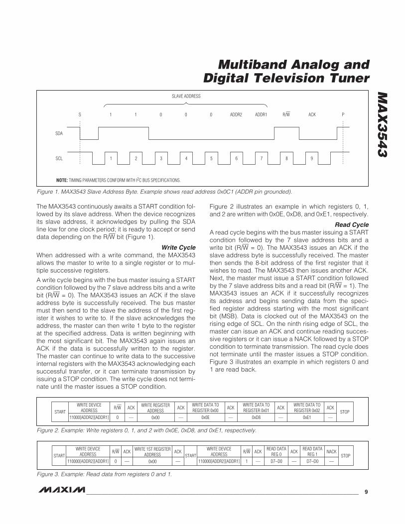
The MAX3543 continuously awaits a START condition fol-lowed by its slave address. When the device recognizes its slave address, it acknowledges by pulling the SDA line low for one clock period; it is ready to accept or send data depending on the R/W bit (Figure 1).
Write CycleWhen addressed with a write command, the MAX3543 allows the master to write to a single register or to mul-tiple successive registers.
A write cycle begins with the bus master issuing a START condition followed by the 7 slave address bits and a write bit (R/W = 0). The MAX3543 issues an ACK if the slave address byte is successfully received. The bus master must then send to the slave the address of the first reg-ister it wishes to write to. If the slave acknowledges the address, the master can then write 1 byte to the register at the specified address. Data is written beginning with the most significant bit. The MAX3543 again issues an ACK if the data is successfully written to the register. The master can continue to write data to the successive internal registers with the MAX3543 acknowledging each successful transfer, or it can terminate transmission by issuing a STOP condition. The write cycle does not termi-nate until the master issues a STOP condition.
Figure 2 illustrates an example in which registers 0, 1, and 2 are written with 0x0E, 0xD8, and 0xE1, respectively.
Read CycleA read cycle begins with the bus master issuing a START condition followed by the 7 slave address bits and a write bit (R/W = 0). The MAX3543 issues an ACK if the slave address byte is successfully received. The master then sends the 8-bit address of the first register that it wishes to read. The MAX3543 then issues another ACK. Next, the master must issue a START condition followed by the 7 slave address bits and a read bit (R/W = 1). The MAX3543 issues an ACK if it successfully recognizes its address and begins sending data from the speci-fied register address starting with the most significant bit (MSB). Data is clocked out of the MAX3543 on the rising edge of SCL. On the ninth rising edge of SCL, the master can issue an ACK and continue reading succes-sive registers or it can issue a NACK followed by a STOP condition to terminate transmission. The read cycle does not terminate until the master issues a STOP condition. Figure 3 illustrates an example in which registers 0 and 1 are read back.
Figure 1. MAX3543 Slave Address Byte. Example shows read address 0x0C1 (ADDR pin grounded).
Figure 2. Example: Write registers 0, 1, and 2 with 0x0E, 0xD8, and 0xE1, respectively.
Figure 3. Example: Read data from registers 0 and 1.
SCL
SDA
1 2 3 4 5 6 7 8 9
S 1 1 0 0 0 ADDR2 ADDR1 R/W ACK
SLAVE ADDRESS
P
NOTE: TIMING PARAMETERS CONFORM WITH I2C BUS SPECIFICATIONS.
START
WRITE DEVICEADDRESS
R/W
11000[ADDR2][ADDR1] 0 —— —— —
WRITE REGISTERADDRESS
0x00
ACK ACK ACK ACK ACKWRITE DATA TOREGISTER 0x00
0x0E
WRITE DATA TOREGISTER 0x01
0xD8
WRITE DATA TOREGISTER 0x02
0xE1STOP
START
WRITE DEVICEADDRESS
R/W
110000[ADDR2][ADDR1]
WRITE DEVICEADDRESS
110000[ADDR2][ADDR1]0 ——
WRITE 1ST REGISTERADDRESS
0x00
ACK NACK
—
ACKREAD DATA
REG 0
D7–D0STOP
R/W
1 —
ACKREAD DATA
REG 1
D7–D0—
ACKSTART
Multiband Analog andDigital Television Tuner
MA
X3
54
3
10 _____________________________________________________________________________________
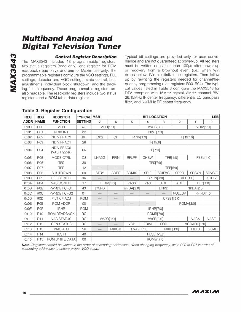
Table 3. Register Configuration
Control Register DescriptionThe MAX3543 includes 18 programmable registers, two status registers (read only), one register for ROM readback (read only), and one for Maxim use only. The programmable registers configure the VCO settings, PLL settings, detector and AGC settings, state control, bias adjustments, individual block shutdown, and the track-ing filter frequency. These programmable registers are also readable. The read-only registers include two status registers and a ROM table data register.
Typical bit settings are provided only for user conve-nience and are not guaranteed at power-up. All registers must be written no earlier than 100Fs after power-up or recovery from a brownout event (i.e., when VCC drops below 1V) to initialize the registers. Then follow up by rewriting the registers needed for channel/fre-quency programming (i.e., registers R00–R04). The typi-cal values listed in Table 3 configure the MAX3543 for DTV reception with 16MHz crystal, 8MHz channel BW, 36.15MHz IF center frequency, differential LC bandpass filter, and 666MHz RF center frequency.
Note: Registers should be written in the order of ascending addresses. When changing frequency, write R00 to R07 in order of ascending addresses to ensure proper VCO setup.
REG ADDR
REG NAME
REGISTER FUNCTION
TYPICAL SETTING
MSB BIT LOCATION LSB
7 6 5 4 3 2 1 0
0x00 R00 VCO 4C VCO[1:0] VSUB[3:0] VDIV[1:0]
0x01 R01 NDIV INT 2B NINT[7:0]
0x02 R02 NDIV FRAC2 8E CPS CP RDIV[1:0] F[19:16]
0x03 R03 NDIV FRAC1 26 F[15:8]
0x04 R04NDIV FRAC0(VAS Trigger)
66 F[7:0]
0x05 R05 MODE CTRL D8 LNA2G RFIN RFLPF CHBW TFB[1:0] IFSEL[1:0]
0x06 R06 TFS 30 TFS[7:0]
0x07 R07 TFP 12 — — TFP[5:0]
0x08 R08 SHUTDOWN 00 STBY SDRF SDMIX SDIF SDIFVG SDPD SDSYN SDVCO
0x09 R09 REF CONFIG 0A — — — CPLIN[1:0] ALC[1:0] XODIV
0x0A R0A VAS CONFIG 17 LFDIV[1:0] VASS VAS ADL ADE LTC[1:0]
0x0B R0B PWRDET CFG1 43 DWPD WPDA[2:0] DNPD NPDA[2:0]
0x0C R0C PWRDET CFG2 01 — — — — — PULLUP RFIFD[1:0]
0x0D R0D FILT CF ADJ ROM — — CFSET[5:0]
0x0E R0E ROM ADDR 00 — — — — ROMA[3:0]
0x0F R0F IRHR ROM IRHR[7:0]
0x10 R10 ROM READBACK RO ROMR[7:0]
0x11 R11 VAS STATUS RO VVCO[1:0] VVSB[3:0] VASA VASE
0x12 R12 GEN STATUS RO — — VCP TRIM POR VCOADC[2:0]
0x13 R13 BIAS ADJ 56 — MIXGM LNA2B[1:0] MIXB[1:0] FILTB IFVGAB
0x14 R14 TEST1 40 RESERVED
0x15 R15 ROM WRITE DATA 00 ROMW[7:0]
Multiband Analog andDigital Television Tuner
MA
X3
54
3
______________________________________________________________________________________ 11
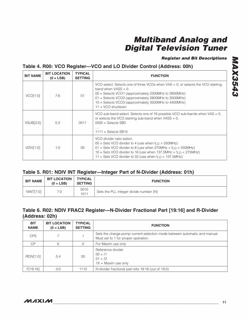
Table 4. R00: VCO Register—VCO and LO Divider Control (Address: 00h)
Table 5. R01: NDIV INT Register—Integer Part of N-Divider (Address: 01h)
Table 6. R02: NDIV FRAC2 Register—N-Divider Fractional Part [19:16] and R-Divider (Address: 02h)
Register and Bit Descriptions
BIT NAMEBIT LOCATION
(0 = LSB)TYPICAL SETTING
FUNCTION
VCO[1:0] 7:6 01
VCO select. Selects one of three VCOs when VAS = 0, or selects the VCO starting band when VASS = 0.00 = Selects VCO1 (approximately 2200MHz to 2800MHz)01 = Selects VCO2 (approximately 2800MHz to 3500MHz)10 = Selects VCO3 (approximately 3500MHz to 4400MHz)11 = VCO shutdown
VSUB[3:0] 5:2 0011
VCO sub-band select. Selects one of 16 possible VCO sub-bands when VAS = 0, or selects the VCO starting sub-band when VASS = 0.0000 = Selects SB0…1111 = Selects SB15
VDIV[1:0] 1:0 00
VCO divider ratio select.00 = Sets VCO divider to 4 (use when fLO > 550MHz)01 = Sets VCO divider to 8 (use when 275MHz < fLO < 550MHz)10 = Sets VCO divider to 16 (use when 137.5MHz < fLO < 275MHz)11 = Sets VCO divider to 32 (use when fLO < 137.5MHz)
BIT NAMEBIT LOCATION
(0 = LSB)TYPICALSETTING
FUNCTION
NINT[7:0] 7:00010 1011
Sets the PLL integer divide number (N)
BIT NAME
BIT LOCATION(0 = LSB)
TYPICAL SETTING
FUNCTION
CPS 7 1Sets the charge-pump current-selection mode between automatic and manual. Must set to 1 for proper operation.
CP 6 0 For Maxim use only
RDIV[1:0] 5:4 00
Reference divider.00 = /101 = /21X = Maxim use only
F[19:16] 3:0 1110 N-divider fractional part bits 19:16 (out of 19:0)
Multiband Analog andDigital Television Tuner
MA
X3
54
3
12 _____________________________________________________________________________________
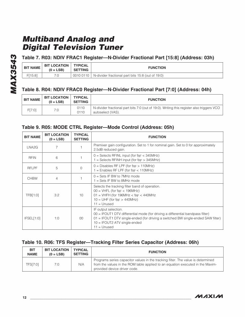
Table 7. R03: NDIV FRAC1 Register—N-Divider Fractional Part [15:8] (Address: 03h)
Table 8. R04: NDIV FRAC0 Register—N-Divider Fractional Part [7:0] (Address: 04h)
Table 9. R05: MODE CTRL Register—Mode Control (Address: 05h)
Table 10. R06: TFS Register—Tracking Filter Series Capacitor (Address: 06h)
BIT NAMEBIT LOCATION
(0 = LSB)TYPICALSETTING
FUNCTION
F[15:8] 7:0 0010 0110 N-divider fractional part bits 15:8 (out of 19:0)
BIT NAMEBIT LOCATION
(0 = LSB)TYPICAL SETTING
FUNCTION
F[7:0] 7:001100110
N-divider fractional part bits 7:0 (out of 19:0). Writing this register also triggers VCO autoselect (VAS).
BIT NAMEBIT LOCATION
(0 = LSB)TYPICAL SETTING
FUNCTION
LNA2G 7 1Premixer gain configuration. Set to 1 for nominal gain. Set to 0 for approximately 2.5dB reduced gain.
RFIN 6 10 = Selects RFINL input (for fRF < 345MHz)1 = Selects RFINH input (for fRF > 345MHz)
RFLPF 5 00 = Disables RF LPF (for fRF > 110MHz)1 = Enables RF LPF (for fRF < 110MHz)
CHBW 4 10 = Sets IF BW to 7MHz mode1 = Sets IF BW to 8MHz mode
TFB[1:0] 3:2 10
Selects the tracking filter band of operation.00 = VHFL (for fRF < 196MHz)01 = VHFH (for 196MHz < fRF < 440MHz10 = UHF (for fRF > 440MHz)11 = Unused
IFSEL[1:0] 1:0 00
IF output selection.00 = IFOUT1 DTV differential mode (for driving a differential bandpass filter)01 = IFOUT1 DTV single-ended (for driving a switched BW single-ended SAW filter)10 = IFOUT2 ATV single-ended11 = Unused
BIT NAME
BIT LOCATION (0 = LSB)
TYPICAL SETTING
FUNCTION
TFS[7:0] 7:0 N/APrograms series capacitor values in the tracking filter. The value is determined from the values in the ROM table applied to an equation executed in the Maxim-provided device driver code.

Multiband Analog andDigital Television Tuner
MA
X3
54
3
______________________________________________________________________________________ 13
Table 11. R07: TFP Register—Tracking Filter Parallel Capacitor (Address: 07h)
Table 12. R08: SHUTDOWN Register—Shutdown Control (Address: 08h)
Table 13. R09: REF CONFIG Register—Reference Oscillator Configuration (Address: 09h)
BIT NAMEBIT LOCATION
(0 = LSB)TYPICAL SETTING
FUNCTION
EMPTY 7:6 00 Empty
TFP[5:0] 5:0 N/APrograms parallel capacitor values in the tracking filter. The value is determined from the values in the ROM table applied to an equation executed in the Maxim-provided device driver code.
BIT NAMEBIT LOCATION
(0 = LSB)TYPICAL SETTING
FUNCTION
STBY 7 0Standby.1 = All circuits shut down except crystal oscillator and REFOUT
SDRF 6 0 RF shutdown. Must set to 0 for proper operation.
SDMIX 5 0 Mixer shutdown. Must set to 0 for proper operation.
SDIF 4 0 IF shutdown. Must set to 0 for proper operation.
SDIFVG 3 0IF VGA shutdown.0 = IF VGA enabled1 = IF VGA disabled
SDPD 2 0 Power-detector shutdown. Must set to 0 for proper operation.
SDSYN 1 0 Frequency synthesizer shutdown. Must set to 0 for proper operation.
SDVCO 0 0 VCO shutdown. Must set to 0 for proper operation.
BIT NAMEBIT LOCATION
(0 = LSB)TYPICAL SETTING
FUNCTION
EMPTY 7:5 000 Empty
CPLIN[1:0] 4:3 01 Must set to 01 for proper operation
ALC[1:0] 2:1 01 Must set to 01 for proper operation
XODIV 0 0Sets crystal oscillator divider for REFOUT signal when REFDIV pin is unconnected.0: fREFOUT = fXTAL/41: fREFOUT = fXTAL

Multiband Analog andDigital Television Tuner
MA
X3
54
3
14 _____________________________________________________________________________________
Table 14. R0A: VAS CONFIG Register—VCO Autoselect Configuration (Address: 0Ah)
Table 15. R0B: PWRDET CFG1 Register—Power-Detector Configuration 1 of 2 (Address: 0Bh)
Note: Only production tested and guaranteed functional in states 0001 0010, 0101 0010, and 1001 0010. All other states are untested and may not function correctly. Contact Maxim if untested settings will be used in production.
Note: Only production tested and guaranteed functional in state X100 X011, where X can be either 0 or 1. All other states are untested and may not function correctly. Contact Maxim if untested settings will be used in production.
BIT NAMEBIT LOCATION
(0 = LSB)TYPICAL SETTING
FUNCTION
LFDIV[1:0] 7:6 00
Sets the low-frequency clock divider.00 = Use for 16MHz P fREF < 20MHz01 = Use for 20MHz P fREF < 28MHz10 = Use for 28MHz P fREF P 32MHz11 = Unused
VASS 5 0
Controls the VCO autoselect (VAS) start conditions function.0 = VAS starts from the current VCO/VCOSB loaded in the VCO[1:0] and VSUB[3:0] bits (in R00)1 = VAS starts from the currently used VCO and VCOSB
VAS 4 1 Controls the VCO autoselect (VAS) function. Must set to 1 for proper operation.
ADL 3 0
Enables or disables the VCO tuning voltage ADC latch when the VCO autoselect (VAS) mode is disabled.0 = Disables the ADC latch1 = Latches the ADC value
ADE 2 0
Enables or disables VCO tuning voltage ADC read when the VCO autoselect (VAS) mode is disabled.0 = Disables ADC read1 = Enables ADC read
LTC[1:0] 1:0 10 Sets the VCO autoselect wait time. Must set to 10 for proper operation.
BIT NAMEBIT LOCATION
(0 = LSB)TYPICAL SETTING
FUNCTION
DWPD 7 0Enables or disables wideband power detector.0 = Enables wideband power detector. Use this state for autonomous RFAGC.1 = Disables wideband power detector
WPDA[2:0] 6:4 100
Sets the wideband power-detector attack point (takeover point).000 = Min100 = Nom (see the Typical Operating Characteristics)111 = Max
DNPD 3 0Enables or disables narrowband power detector.0 = Enables narrowband detector. Use this state for autonomous RFAGC.1 = Disables narrowband detector
NPDA[2:0] 2:0 011
Sets the narrowband power-detector attack point (takeover point).000 = Min011 = Nom (see the Typical Operating Characteristics)111 = Max
Multiband Analog andDigital Television Tuner
MA
X3
54
3
______________________________________________________________________________________ 15
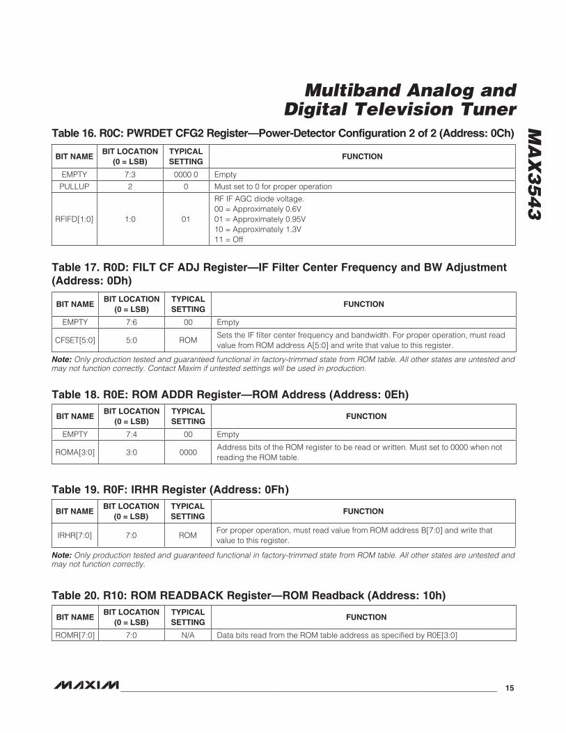
Table 16. R0C: PWRDET CFG2 Register—Power-Detector Configuration 2 of 2 (Address: 0Ch)
Table 17. R0D: FILT CF ADJ Register—IF Filter Center Frequency and BW Adjustment (Address: 0Dh)
Table 18. R0E: ROM ADDR Register—ROM Address (Address: 0Eh)
Table 19. R0F: IRHR Register (Address: 0Fh )
Table 20. R10: ROM READBACK Register—ROM Readback (Address: 10h)
Note: Only production tested and guaranteed functional in factory-trimmed state from ROM table. All other states are untested and may not function correctly. Contact Maxim if untested settings will be used in production.
Note: Only production tested and guaranteed functional in factory-trimmed state from ROM table. All other states are untested and may not function correctly.
BIT NAMEBIT LOCATION
(0 = LSB)TYPICAL SETTING
FUNCTION
EMPTY 7:3 0000 0 Empty
PULLUP 2 0 Must set to 0 for proper operation
RFIFD[1:0] 1:0 01
RF IF AGC diode voltage.00 = Approximately 0.6V01 = Approximately 0.95V10 = Approximately 1.3V11 = Off
BIT NAMEBIT LOCATION
(0 = LSB)TYPICAL SETTING
FUNCTION
EMPTY 7:6 00 Empty
CFSET[5:0] 5:0 ROMSets the IF filter center frequency and bandwidth. For proper operation, must read value from ROM address A[5:0] and write that value to this register.
BIT NAMEBIT LOCATION
(0 = LSB)TYPICAL SETTING
FUNCTION
EMPTY 7:4 00 Empty
ROMA[3:0] 3:0 0000Address bits of the ROM register to be read or written. Must set to 0000 when not reading the ROM table.
BIT NAMEBIT LOCATION
(0 = LSB)TYPICAL SETTING
FUNCTION
IRHR[7:0] 7:0 ROMFor proper operation, must read value from ROM address B[7:0] and write that value to this register.
BIT NAMEBIT LOCATION
(0 = LSB)TYPICAL SETTING
FUNCTION
ROMR[7:0] 7:0 N/A Data bits read from the ROM table address as specified by R0E[3:0]

Multiband Analog andDigital Television Tuner
MA
X3
54
3
16 _____________________________________________________________________________________
Table 21. R11: VAS STATUS Register—VCO Autoselect Status (Address: 11h)
Table 22. R12: GEN STATUS Register—General Status (Address: 12h)
Table 23. R13: BIAS ADJ Register—Bias Adjustments (Address: 13h)
Note: Not production tested or guaranteed functional.
Note: Not production tested or guaranteed functional.
Note: Only production tested and guaranteed functional in state 0XX1 X11X, where X can be either 0 or 1. All other states are untested and may not function correctly. Contact Maxim if untested settings will be used in production.
BIT NAMEBIT LOCATION
(0 = LSB)TYPICAL SETTING
FUNCTION
VVCO[1:0] 7:6 N/AIndicates which VCO has been selected by either the autoselect state machine or by manual selection when the VSA state machine is disabled. See the R00 description for the VCO[1:0] definition.
VVSB[3:0] 5:2 N/AIndicates which sub-band of a particular VCO has been selected by either the autoselect state machine or by manual selection when the VSA state machine is disabled. See the R00 description for the VSUB[3:0] definition.
VASA 1 N/AIndicates whether VCO autoselection was successful.0 = Indicates the autoselect function is disabled or unsuccessful VCO selection1 = Indicates successful VCO autoselection
VASE 0 N/AStatus indicator for the autoselect function.0 = Indicates the autoselect function is active1 = Indicates the autoselect process is inactive
BIT NAMEBIT LOCATION
(0 = LSB)TYPICAL SETTING
FUNCTION
EMPTY 7:6 N/A Empty
VCP 5 N/A Maxim use only
TRIM 4 N/A Maxim use only
POR 3 N/A Maxim use only
VCOADC [2:0]
2:0 N/A
VCO tuning voltage indicators.000 = PLL not in lock, tune to the next lowest sub-band001 to 110 = PLL in lock111 = PLL not in lock, tune to the next higher sub-band
BIT NAMEBIT LOCATION
(0 = LSB)TYPICAL SETTING
FUNCTION
EMPTY 7 0 Empty
MIXGM 6 1 Mixer gain setting. Set to 0 for ATV mode. Set to 1 for DTV mode.
LNA2B[1:0] 5:4 01
LNA bias.00 = Unused01 = Nominal setting. Use for all standards except SECAM L/L’.10 = Unused11 = Highest linearity setting. Use for SECAM L/L’.
MIXB[1:0] 3:2 01
Mixer bias.00 = Unused01 = Nominal setting. Use for all standards except SECAM L/L’.10 = Unused11 = Highest linearity setting. Use for SECAM L/L’.
FILTB 1 1 Must set to 1 for proper operation
IFVGAB 0 0IF VGA bias.0 = Default1 = Highest current (approximately nominal + 6mA)

Multiband Analog andDigital Television Tuner
MA
X3
54
3
______________________________________________________________________________________ 17
Applications InformationRF Inputs and Filters
The MAX3543 features separate low- and high-frequency inputs. These two inputs are combined to a single input by an off-chip diplexer circuit as shown in the Typical Application Circuit. When the desired channel is less than 345MHz, use RFINL. When the desired input is greater than 345MHz, use RFINH. Further, when the desired input is less than 110MHz, an internal lowpass filter should be enabled to limit high-frequency interfer-ence incident at the mixer input. The lowpass filter is enabled by the RFLPF bit in R05[5].
Besides selecting the appropriate input port and setting RFLPF appropriately, one of three tracking filters must be chosen based on the desired frequency. Set TFB (R05[3:2]) to select VHFL, VHFH, or UHF tracking filter bands. Use VHFL when the desired frequency is less than 196MHz, use VHFH when the desired frequency is between 196MHz and 440MHz, or use UHF when the desired frequency is greater than 440MHz.
RF Gain ControlThe MAX3543 is designed to control its own RF gain based on internally measured signal and blocker levels. The user can adjust the AGC attack points (takeover points) by setting WDPA and NDPA in register R0B. Alternatively, the user can control the RF gain by driving the RFVGC input pin.
VCO and VCO Divider SelectionThe MAX3543 frequency synthesizer includes three VCOs with 16 sub-bands for each VCO. These VCOs and sub-bands are selected to best center the VCO near the operating frequency. This selection process is performed automatically by the VAS circuitry. The Maxim driver software seeds the VCO starting band for fastest selection time.
In addition to VCO selection, a VCO divider value of 32, 16, 8, or 4 must be selected to provide the desired mixer LO drive frequency. The divider is selected by VDIV in register R00[1:0].
Reading the ROM TableThe MAX3543 includes 13 ROM registers to store fac-tory calibration data (see Table 26). Each ROM table entry must be read using a two-step process. First, the address of the ROM bits to be read must be pro-grammed into the ROM ADDR register (R0E[3:0]).
Once the address has been programmed, the data stored in that address is automatically transferred to the ROM READBACK register (R10[7:0]). The ROM data at the specified address can then be read from the ROM READBACK register and stored in the microprocessor’s local memory. After all ROM registers have been read and stored in the microprocessor’s local memory, ROM ADDR must be programmed to 00 for proper operation.
Table 24. R14: TEST1 Register (Address: 14h)
Table 25. R15: ROM WRITE DATA Register (Address: 15h)
Note: This register is not available to the end user.
Note: This register is not available to the end user.
BIT NAMEBIT LOCATION
(0 = LSB)TYPICAL SETTING
FUNCTION
RESERVED 7:001000000
Must set to 0100 0000 for proper operation
BIT NAMEBIT LOCATION
(0 = LSB)TYPICAL SETTING
FUNCTION
ROMW[7:0] 7:0 N/A Maxim use only

Multiband Analog andDigital Television Tuner
MA
X3
54
3
18 _____________________________________________________________________________________
Setting RF Tracking Filter CodesThe MAX3543 includes a programmable tracking filter for each band of operation to optimize rejection of out-of-band interference while minimizing insertion loss for the desired received signal. The center frequency of each tracking filter is selected by a switched-capacitor array that is programmed by the TFS[7:0] bits in the R06 register and the TFP[5:0] bits in the R07 register.
Optimal tracking filter settings for each channel vary from part to part due to process variations. To accommodate part-to-part variations, each part is factory calibrated by Maxim. During calibration the correction factors for the series and parallel tracking capacitor arrays are calculat-ed and written into an internal ROM table. The user must read the ROM table upon power-up and store the data in local memory (8 bytes total) to calculate the optimal TFS and TFP settings for each channel. The equation for setting TFS and TFP at each channel is available in the device driver code provided by Maxim. Table 26 shows the address and bits for each ROM table entry.
Layout RecommendationsIMPORTANT: The MAX3543 includes on-chip tracking filters that utilize external inductors placed on the PCB at pins 30 through 37. Because the tracking filters oper-ate at frequencies up to 862MHz, they are sensitive to the inductor and PCB trace parasitics. To achieve the optimal RF performance (gain, noise figure, and image rejection), MAX3543 is production tested and trimmed with the exact same inductors, their relative location
and orientation, and the trace parasitics present on the MAX3543 Reference Design. To avoid performance deg-radation, PCB designs should exactly copy the RF sec-tion of the Reference Design layout and use the induc-tors specified in the Reference Design bill of materials. Contact Maxim to obtain the Reference Design layout to use as a starting point for PCB designs.
In addition to the aforementioned requirements, follow general good RF layout practices. Keep RF signal lines as short as possible to minimize losses and radiation. Use controlled impedance on all high-frequency traces. The exposed paddle must be soldered evenly to the board’s ground plane for proper operation. Use abun-dant vias beneath the exposed paddle and maximize the area of continuous ground plane around the paddle on the bottom layer for maximum heat dissipation. Use abundant ground vias between RF traces to minimize undesired coupling.
To minimize coupling between different sections of the IC, the ideal power-supply layout is a star configura-tion, which has a large decoupling capacitor at the central VCC node. The VCC traces branch out from this node, with each trace going to separate VCC pins of the MAX3543. Each VCC pin must have a bypass capacitor with a low impedance to ground at the frequency of inter-est. Do not share ground vias among multiple connec-tions to the PCB ground plane.
Table 26. ROM TableDESCRIPTION ADDR MSB DATA BYTE LSB
BIAS 0x0 Unused BIAS[3:0]
VHF-Low Tracking Filter.VLS0, VLS1, VLP0, VLP1
0x1 VLS0[5] VLS0[4] VLS0[3] VLS0[2] VLS0[1] VLS0[0] VLS1[5] VLS1[4]
0x2 VLS1[3] VLS1[2] VLS1[1] VLS1[0] VLP0[5] VLP0[4] VLP0[3] VLP0[2]
0x3 VLP0[1] VLP0[0] VLP1[5] VLP1[4] VLP1[3] VLP1[2] VLP1[1] VLP1[0]
VHF-High Tracking Filter.VHS0, VHS1, VHP0, VHP1
0x4 VHS0[5] VHS0[4] VHS0[3] VHS0[2] VHS0[1] VHS0[0] VHS1[5] VHS1[4]
0x5 VHS1[3] VHS1[2] VHS1[1] VHS1[0] VHP0[5] VHP0[4] VHP0[3] VHP0[2]
0x6 VHP0[1] VHP0[0] VHP1[5] VHP1[4] VHP1[3] VHP1[2] VHP1[1] VHP1[0]
UHF Tracking Filter.US0, US1, UP0, UP1
0x7 US0[5] US0[4] US0[3] US0[2] US0[1] US0[0] US1[5] US1[4]
0x8 US1[3] US1[2] US1[1] US1[0] UP0[5] UP0[4] UP0[3] UP0[2]
0x9 UP0[1] UP0[0] UP1[5] UP1[4] UP1[3] UP1[2] UP1[1] UP1[0]
IF Filter 0xA Unused Unused C[5] C[4] C[3] C[2] C[1] C[0]
IRHR 0xB IRHR[7] IRHR[6] IRHR[5] IRHR[4] IRHR[3] IRHR[2] IRHR[1] IRHR[0]
Reserved 0xC Reserved Reserved Reserved Reserved Reserved Reserved Reserved Reserved

Multiband Analog andDigital Television Tuner
MA
X3
54
3
______________________________________________________________________________________ 19
Package InformationFor the latest package outline information and land patterns, go to www.maxim-ic.com/packages. Note that a “+”, “#”, or “-” in the package code indicates RoHS status only. Package drawings may show a different suffix character, but the drawing pertains to the package regardless of RoHS status.
PACKAGE TYPE PACKAGE CODE OUTLINE NO. LAND PATTERN NO.
40 TQFN-EP T4066+2 21-0141 90-0053

Multiband Analog andDigital Television Tuner
MA
X3
54
3
Maxim cannot assume responsibility for use of any circuitry other than circuitry entirely embodied in a Maxim product. No circuit patent licenses are implied. Maxim reserves the right to change the circuitry and specifications without notice at any time.
20 Maxim Integrated Products, 120 San Gabriel Drive, Sunnyvale, CA 94086 408-737-7600© 2010 Maxim Integrated Products Maxim is a registered trademark of Maxim Integrated Products, Inc.
Revision History
REVISIONNUMBER
REVISION DATE
DESCRIPTIONPAGES
CHANGED
0 10/09 Initial release —
1 4/10Updated Applications, extended Frequency specification in AC Electrical Characteristics, and updated Tables 14, 15, and 23 to enable some features
1, 3, 14, 16
2 7/10 Corrected Figure 3 9