multi-gb/s serial channel design using a hybrid ... using a hybrid measurement and simulation...
TRANSCRIPT

DesignCon 2008
Multi-GB/s Serial Channel Design Using a Hybrid Measurement and Simulation Platform Andrew Byers, Ansoft Corporation [email protected] Dima Smolyansky, Tektronix [email protected] Eugene Mayevskiy, Tektronix [email protected]
Will Miller, Efficere Technologies [email protected]

Abstract As emerging communication standards push the data rates of serial channels well into the multi-GB range, a great opportunity arises to streamline and tune system design procedures to achieve both the highly-accurate results demanded by the specifications as well as the first-pass success required by project timelines. A channel design platform which encompasses both measurement and simulation can significantly aid in guiding a project from conception to physical verification. Author Biographies Andrew Byers is a Senior Application Engineer for Ansoft Corporation, based in Beaverton, OR. He helps engineer apply Ansoft high-frequency tools in the computing, communications, and wireless markets. Prior to joining Ansoft, Andrew worked for Tektronix designing high-speed interconnect structures and developing EM-based modeling and simulation capabilities. He holds a BSEE ('98) and MSEE ('00) from the University of Colorado at Boulder. He has authored several papers for journals and conferences and given lectures to international audiences on advanced signal and power integrity. Dima Smolyansky has spent his professional career in the instrumentation and measurement industry, working with high-speed time domain reflectometry oscilloscopes and frequency domain network analyzers. He is responsible for TDR, S-parameter and jitter measurement solutions at Tektronix. Mr. Smolyansky has accumulated significant experience in the area of high-speed digital interconnect measurements and modeling. He has published a number of papers and taught short courses on interconnect measurements and modeling. He holds the M.S.E.E. degree from Oregon State University and the Engineer Diploma (M.S.) degree from Kiev Polytechnic Institute. Eugene Mayevskiy holds the B.S.E.E and M.S.E.E. degrees from Oregon State University where he has done substantial research on measurement-based modeling and analysis of passive devices fabricated for radio frequency integrated circuits. He is currently with Tektronix working on leading interconnect signal integrity and failure analysis products. His responsibilities include product development, training and problem resolution for TDR/VNA measurement, modeling and SPICE/IBIS circuit simulation. He has published a number of papers and given seminars on measurement-based modeling for high-speed designs. Will Miller is CTO and acting Vice President of Engineering at Efficere Technologies and has over 25 years of high performance design and simulation of very high-performance semiconductor automatic test equipment and advanced electro-optical instrumentation for aerospace and commercial applications at companies such as Integrated Measurement Systems and Credence. He has developed manufacturing techniques for precision high performance electronic signals on electronic substrates. He joined Efficere in 2005 to lead the company’s engineering efforts in advanced test, memory module, power subsystem, and interconnect/cable/receptacle design. He holds one US patent and has authored several more.
Introduction Engineers designing servers, storage devices, multimedia PCs, gaming, entertainment, and telecom systems, apply standard interfaces such as XAUI, XFI, Serial ATA, PCI Express, HDMI, and FB-DIMM to achieve serial signaling rates up to 10 GB/s using high speed, point-to-point serial buses. To assure that signals are being reliably transmitted across these high speed serial buses, signal integrity engineers must identify and resolve the principle causes of poor signal timing and quality—reflection, crosstalk, and simultaneous switching noise. Because these faults are difficult to diagnose after the system is built and because re-spins can be extremely expensive, signal integrity engineers rely on simulations prior to tape-out to discover potential faults. There are many challenges, however, to achieving a simulation that accurately predicts system level behavior. For example, getting the data needed to construct a model can sometimes prove daunting. For competitive reasons, vendors, on occasion, will refuse to divulge the details of their components. Encryption often suffices for active device circuitry, but how does a vendor protect the dielectric constant of a proprietary connector material? These challenges are forcing the adoption of new strategies and tools. This paper addresses these concerns by outlining a set of tools and methods that meet the challenges and demonstrating them in a relevant test case. The key element of the approach presented in this paper is the combination of measurement-based models with EM-extracted models. After a discussion of various design trade-offs, simulated and measured results are presented. Background A “platform” as used in the context of this paper is of a collection of tools and methods used to design, verify, and optimize high-speed serial data channels. Traditionally, these tools and methods have consisted of simulation software and measurement instrumentation that have been used independently to validate designs. A “hybrid platform” is a modular approach that integrates both simulation software and instrumentation technologies into a single design flow. The terms “hybrid platform” and “modular platform” will be used interchangeably. While “high-speed” is a relative term, it is intended here to represent any current interface with a transmission rate in the multi-GB/s range. A key benefit of the modular design platform explored in this paper is the ability to create a reconfigurable simulation test bench for testing an unlimited variety of serial channels. Such a test bench was used to test the channel models presented in this paper. Secondary benefits are accuracy and speed. Accuracy derives from the use of S-parameters which are essential to capturing the coupling behavior among all elements of a high speed channel. Circuit simulators are well known for the speed in which they can produce results. When S-parameter based models are coupled with advanced circuit simulation, the modeling gains in both dimensions.

When validating high speed serial channels, accuracy in both time- and frequency-domain is critical for every element in the channel. To accomplish this, it is imperative that all models have sufficient bandwidth to cover the frequency content of the transient signals. The channel’s DC characteristics, which are often extrapolated, are also important. Poor extrapolation or extraction techniques to DC can result in non-physical behavior—which appears as an exponential rise near DC in transient simulations. Additionally, causality violations can sometimes occur in transient simulation if proper care is not taken in the numerical implementation. These violations can be avoided by using appropriate frequency-dependent material properties in the EM-extraction tool or making causality corrections in the time-domain model implementation. Electromagnetic field simulation using 3D full-wave techniques provides GHz-accurate S-parameter and Full-Wave Spice™ models for complex trace routing, vias and transitions, connectors, and IC packages. Traditional approaches have relied on SPICE techniques to provide transient simulation of high speed channels. Lumped equivalent circuits for interconnect elements derived by static field simulations, measurements, or analytical means have been cascaded in SPICE to simulate overall channel response. SPICE simulation has the added benefit of allowing engineers to include nonlinear transistor-level circuits for drivers and receivers providing a more accurate representation of interconnect performance. However, traditional SPICE simulation with lumped equivalent circuits and simplified transmission line models become unacceptably inaccurate for multi-GB/s channels. In this realm, S-parameters provide the best representation of the distributed nature of very high-speed interconnects. For this study, HFSS™ was used to extract S-parameter models. The virtual “hub” of the design is the circuit, or system, simulation environment. This hub serves as a means to manage models, experiments, and output. In a real sense, this system-level design environment is the foundation for the platform, while the model extraction techniques are complementary elements. Important considerations for choosing a circuit (system) simulation tool are capacity, reliability, and the ability to simulate in both time- and frequency-domains. Channel paths combining transistor-level models of transceivers, pre-emphasis circuits, and equalizers with extracted interconnect models create challenging simulation netlists. S-parameters, transmission line models, and tens of thousands of circuit elements require advanced circuit simulation technology. What is needed for simulation of multi-GB/s channels is full-wave field solvers integrated with a circuit simulator that provides the reliability and capacity required for modern serial channel analysis. In addition, GHz designs must include frequency- and time-domain simulations to predict system performance correctly. High-performance electronic designs often include operating specifications for power integrity in the frequency-domain and for signal integrity in the time-domain. Common time-domain metrics like eye-diagrams, jitter, TDR measurements, and SSO and frequency domain metrics like resonances, phase noise margins, power plane impedance, and insertion losses appear within the same spec sheet. In this study, Ansoft Designer™ was used to provide the front-end design management and post-processing and Nexxim® was used as the circuit simulation engine.

Like simulation tools, measurement tools and methods must also evolve to keep pace with the speeds and requirements of the new data communication specifications. One such methodology that can be used in a signal integrity engineer’s platform is time-domain network analysis (TNDA). TDNA utilizes time-domain based TDR and TDT measurements combined with advanced software solutions to provide quick and accurate S-parameter measurements, equivalent model extraction, and full-channel characterization. The specific TDNA-based tool that we chose for this project was Iconnect® by Tektronix [1]. Iconnect can be used to perform single-ended, differential, and mixed mode S-parameter measurements of the channel and conduct interconnect electrical standard compliance testing on eye diagrams.
Figure 1: Depiction of TDR-based equivalent SPICE model creation using Iconnect A feature of this tool that allows for its use in a larger system-level design platform is its ability to quickly and easily generate SPICE and IBIS models for various components in the channel. This procedure involves partitioning a TDR-based impedance profile plot into separate sections, with each section defined by a time delay and impedance value. Each of these sections is then written out into a SPICE file of cascaded circuit elements. This procedure is depicted in Figure 1 above. The advantage of being able to extract a circuit model from a TDR-based measurement is that missing or previously unavailable S-parameter models can now be extracted. Figure 2 illustrates this concept. In this example, the unavailable component is a connector. Normally, this connector would have a 3D CAD model associated with it which would be imported into a 3D EM simulator tool and an S-parameter model would then be extracted. However, in many instances, the connector vendor cannot or will not release this data. In this situation, an Iconnect procedure on a prototype connector can yield an equivalent model which can be inserted into the circuit simulation.

Figure 2: Typical scenario in which an interconnect component model is unavailable.
Validation In the validation tests that follow, self-consistency between HFSS and TDR derived S-parameters is demonstrated. Two test cases were chosen: a microstrip impedance step structure and a microstrip Cheybyshev filter design. Both channels were placed on standard FR4 dielectric and measurements and simulations were performed up to 20 GHz. The microstrip impedance step device contained three series connected traces: a 0.19mm wide microstrip trace followed by a 0.55mm wide trace followed by another 0.19mm trace. The effective structure is a lower impedance transmission line sandwiched between two higher impedance lines. The dielectric height of the FR4 substrate was 0.1125mm and a soldermask was present. HFSS was used to produce W-element transmission-line models. These models were cascaded in Ansoft Designer and simulated with Nexxim to produce both time- and frequency-domain waveforms. Similarly, both time- and frequency-domain curves are produced from the quick TDR measurements using Iconnect. Measurement and simulation results are compared in Figure 3.

Figure 3: Microstrip impedance step structure simulation vs. TDR-based measurement. In the second validation test, the Chebyshev filter is characterized. Both the 3D EM simulation and the TDR measurements included SMA connectors installed on the backside of the PCB. The HFSS model of the Chebyshev filter structure is shown in Figure 4. Figure 4 also includes the S21, or insertion loss, results of both measurement and simulation. Up to 10GHz the results were extremely close, and the filter effect begins at almost exactly the same frequency. Note the beginnings of discrepancies seen in the filter response above 10GHz. These could be due to simplifying assumptions made to the SMA model, variations in the geometric details of the measured filter, or complex frequency-dependent artifacts seen in the FR4 material. However, the salient match of simulation to measurement was sufficient for this phase of the study.
Figure 4: Microstrip Chebyshev filter HFSS model and comparison to measured results for S21.
FR4 Dielectric:thickness = 4.4 miler = 4.2tand = 0.02
SMA connections on backsideof PCB
Ansoft SimulationTDR-based S-parameters
Filter Insertion Loss
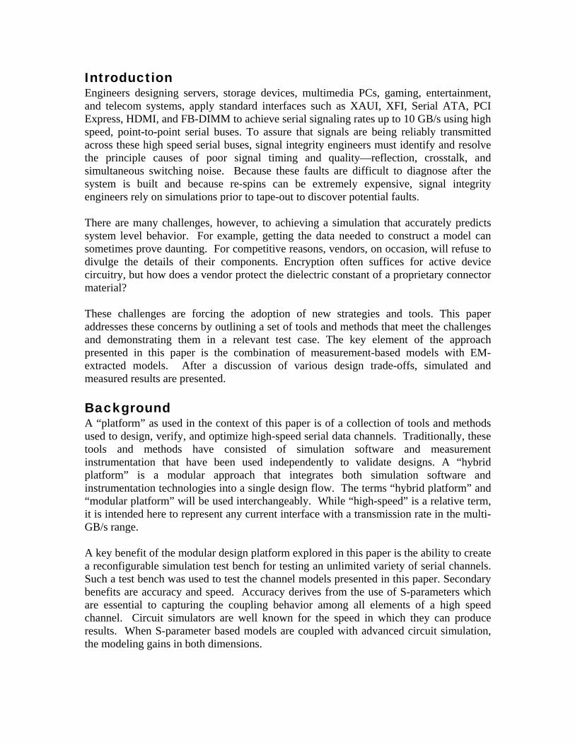
HDMI Test Case To test the hybrid platform, a high-definition multi-media interface (HDMI) channel consisting of two adapters and a cable assembly was selected. The HDMI specification is a licensed technology used for building audio/video systems that transmit high-speed digital data [2]. An HDMI system uses transition-minimized differential signaling (TMDS) to send its digital content from element to element. A commonly-used version of HDMI is v1.2, which uses a single-link clock rate of 165 MHz and thus a single-lane bit rate of 1.65GB/s for the 10-bit-per-clock-cycle data lanes. To support high frame rates and better resolution, the newer v1.3 spec increases the single-link clock rate to 340 MHz and the data rate to 3.4 GB/s. For some applications, twisted pair cables are used between HDMI system components. However, for long distance applications and/or higher-quality products, bundled coaxial cable assemblies are preferred. Coax was used in this study. The HDMI channel shown in Figure 5 below was chosen because it includes both electrically small details (adapter, transitions) as well as longer, lossy channel components (cable). The combination of these components was deemed a robust test of the hybrid platform approach. The modular nature of the platform is demonstrated through the use of models from several different sources. The instrument used to produce the TDR measurements was the Tektronix DSA8200 using 80E10 sampling heads. These sampling heads provide for 12ps rise times and excellent intra-pair matching for true differential signaling. Models for each of the components in this system were extracted and compared to measurements. Use of the platform to aid in analysis of the individual components as well as exploration of the full-channel design space will be shown.
Figure 5: HDMI test case representation.

There are several technical challenges common to high speed channels that can be addressed with the platform presented herein. Signal or reference plane transitions form the most significant roadblock to quality signal integrity in all high-speed systems. As signal lines move from one environment to another, both the signal and return paths tend to be broken, which result in reflections, loss, increased coupling, and possibly unintended radiation. The transitions seen in typical HDMI assemblies include SMA cable-to-cable connections, coax-to-adapter launches, and HDMI-specific cable connectors. In order to connect the DUT and test instrumentation, a flexible and electrically transparent adapter is needed. The selected adapter is designed and produced by Efficere Technologies [3], and is shown in Figure 6. This adapter provides a high-performance connection between the test instrument coax cable and the HDMI device or cable. Matched lengths of microstrip transmission lines minimize skew across the adapter substrate. Identical length microstrip lines with various terminations (SOLT) on the same substrate can also be used for calibration as needed.
Figure 6 : HDMI Type-A adapter.
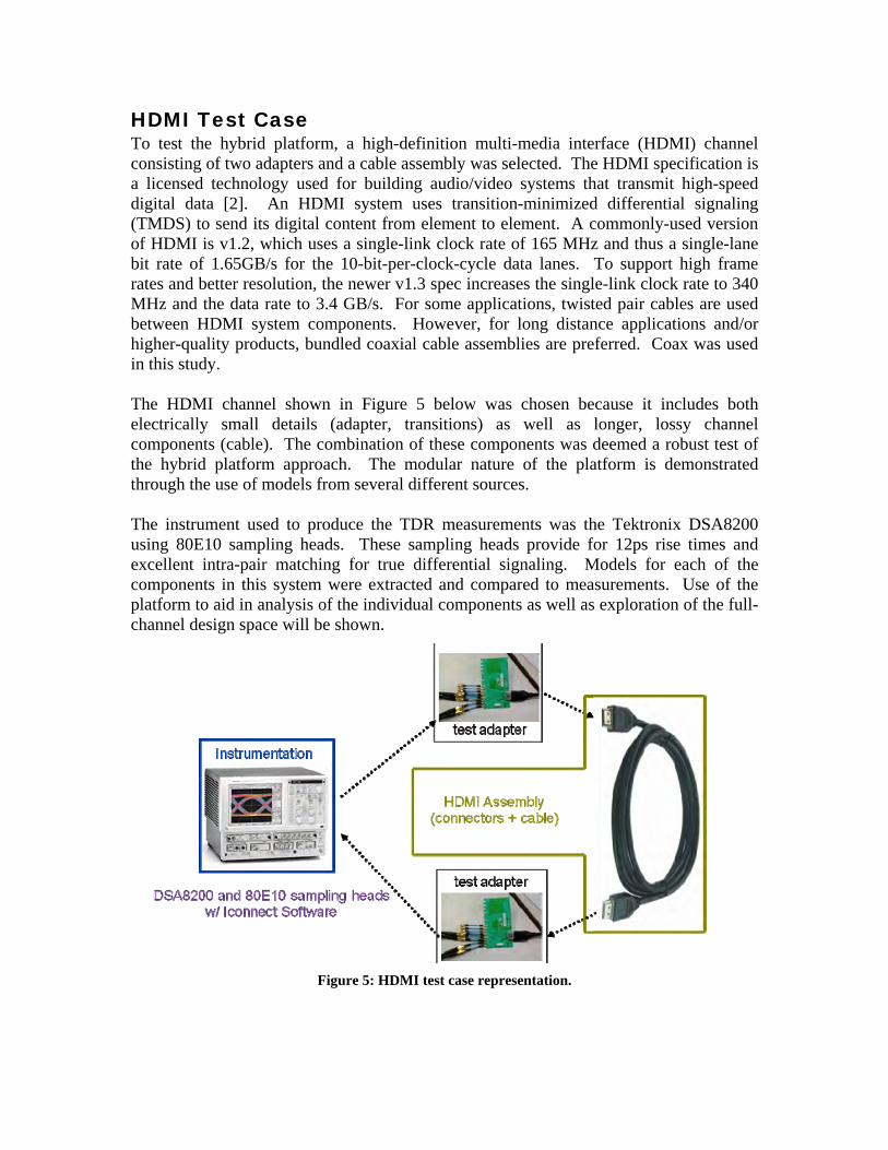
The element that contributes the most to signal loss in these systems is the cable. Although per-unit-length loss of HDMI cables is typically very small compared to microstrips or striplines, the relatively long lengths of HDMI cable (sometimes ranging to 100 feet) pose a significant challenge. Challenges in dealing with this loss extend to simulation as well. While linear frequency-domain simulations of long cables are straightforward, handling them in transient simulation becomes more difficult. Long delays appear as rapid phase changes in the frequency domain and these create special challenges for the two algorithms employed in the transient simulation of S-parameters. The method used for this paper was convolution. For this method, it is necessary to have sufficiently dense frequency-domain data so as to avoid aliasing the long delay into
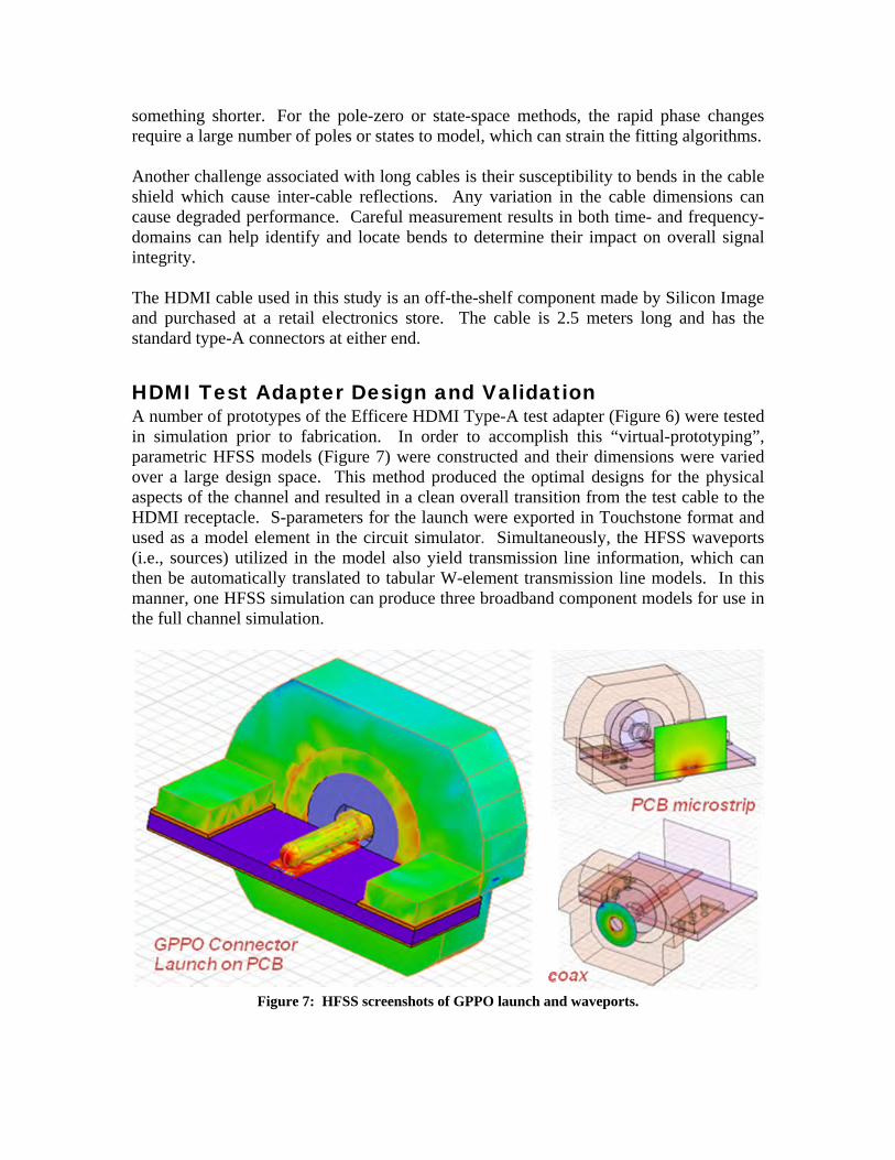
something shorter. For the pole-zero or state-space methods, the rapid phase changes require a large number of poles or states to model, which can strain the fitting algorithms. Another challenge associated with long cables is their susceptibility to bends in the cable shield which cause inter-cable reflections. Any variation in the cable dimensions can cause degraded performance. Careful measurement results in both time- and frequency-domains can help identify and locate bends to determine their impact on overall signal integrity. The HDMI cable used in this study is an off-the-shelf component made by Silicon Image and purchased at a retail electronics store. The cable is 2.5 meters long and has the standard type-A connectors at either end. HDMI Test Adapter Design and Validation A number of prototypes of the Efficere HDMI Type-A test adapter (Figure 6) were tested in simulation prior to fabrication. In order to accomplish this “virtual-prototyping”, parametric HFSS models (Figure 7) were constructed and their dimensions were varied over a large design space. This method produced the optimal designs for the physical aspects of the channel and resulted in a clean overall transition from the test cable to the HDMI receptacle. S-parameters for the launch were exported in Touchstone format and used as a model element in the circuit simulator. Simultaneously, the HFSS waveports (i.e., sources) utilized in the model also yield transmission line information, which can then be automatically translated to tabular W-element transmission line models. In this manner, one HFSS simulation can produce three broadband component models for use in the full channel simulation.
Figure 7: HFSS screenshots of GPPO launch and waveports.

As sometimes happens, models for the HDMI connector and the SMA connector were not available. However, because a physical prototype of the adapter had already been built, TDR was used to measure the actual component and Iconnect was used to produce SPICE-formatted sub-circuit models for these structures. These models were subsequently imported into the circuit simulator and cascaded with the other channel components. The full channel is shown in Figure 8. With this simulation channel now completed, various what-if scenarios, cost reduction studies, and next-generation system development can be explored.
Figure 8: HDMI Type-A Adapter channel schematic in Ansoft Designer.
A TDR comparison between our hybrid simulation and the full measurement is shown in Figure 9. Note the excellent agreement seen in the impedances of the transmission line segments and the GPPO launch model. As expected, the most significant source of reflection in the TDR signature involves the HDMI connector.
Figure 9: Comparison of TDR measured vs. modeled HDMI adapter.
The next element of the HDMI assembly to be studied is the long coaxial cable. Most cables used for HDMI systems use 23 or 24AWG conductors and a Polyolefin-type
dielectric [4]. Because the actual dimensions of the off-the-shelf coax cable used in this study were not known, an electrical model was derived. Starting with best-guess estimates, the dielectric constant and loss tangent were swept in a waveport solution in HFSS until the characteristic impedance and attenuation closely matched quoted specs and measured values. The final dimensions obtained were inner radius of 22mil, outer radius of 74 mil, dielectric constant of 2.1 and loss tangent of 0.008. Crosstalk between pairs was not considered as part of this study as most cable vendors quote this spec at less than -30dB up to several GHz. A common-mode crosstalk study would include modeling all coax cables in the HDMI bundle as well as their touching return paths. However, the extreme variability in cable orientation along the length of the total bundle makes this difficult to model using a fixed-geometry approach. One solution to this problem might be to perform a measurement study of a significant number of samples to determine average crosstalk margins. Another approach would be to create a statistical study in simulation which correlates crosstalk numbers to variations in cable dimensions based on actual cross-sectional measurements. Tinned copper is typically used for the conductors which reduces path losses by a few percent. Using the tables given in [5] for 23 and 24 AWG, tinned-copper is about 3% higher in conductivity than regular, un-tinned copper. For completeness, the model’s material properties were adjusted to reflect these variations, although their impact is not significant. Another important issue to consider when modeling long transmission lines is causality. Careful modeling of the material parameters of the transmission lines is critical to ensure that the transient simulation results in causal behavior. In this case, use of a Djordjevic-Sarkar formulation [6] for the coax dielectric in the HFSS simulation yields a causal tabular W-element model for use in the transient simulation.

Figure 10: TDR and VNA measurement setup for the HDMI assembly. Both VNA and TDR-based measurements were made of the entire assembly. In order to cover the first and third harmonics for HDMI v1.2, measurements up to 5GHz were taken. The measurement setups are shown in Figure 10 and the VNA vs. TDR-based |S21| in Figure 11. The nearly identical plots speak to the accuracy of the measurements and the validity of the TDR-based technique. Comparison of the TDR-based |S21| to the full-channel simulation result is shown in Figure 12. Also shown in this plot is the simulation result without the adapters, which provides a quick de-embedded S-parameter estimate.

Figure 11: TDR-based and VNA |S21| results for 2.5m HDMI channel. Figure 12. Frequency-domain (|S21|) results for HDMI assembly. VNA, TDR-based, and simulation
S-parameters shown.
TDR-based VNA

Another important measurement for multi-GB/s channels is the full channel response observed in an eye diagram. Eye diagrams help a designer to quickly measure characteristics such as jitter, eye opening, and mask violations. In accordance with the HDMI spec, a minimum 400mV swing PRBS-11 bit-pattern controlled switch structure at the transmitter and a pull-up resistor pair at the receiver were used. Figure 13 depicts the schematic used for this simulation, and Figure 14 shows the eye diagram result. The HDMI mask is shown on this eye diagram; it is clear there are no mask violations.
Figure 13: Full HDMI assembly schematic.
Figure 14: Eye-diagram plot from HDMI assembly simulation. Observed channel indicates no mask violations.

Extending the Platform – What-if Analyses The first what-if analysis was to vary the cable line length and record the impact on insertion loss (S21) and eye opening. Figure 15 illustrates the observed relationship. The eye opening and the first harmonic’s (825MHz) S21 both trend downward with roughly the same slope. This observation which appears in both domains can lead to the development of new and useful design guidelines for channel developers. A cornerstone of this multi-GB/s design platform is the importance of both time- and frequency-domain analyses; its underlying circuit simulation engine (Nexxim) ensures equivalence between the two. The same study produced the graph shown in Figure 16, which illustrates the relationship between S21 and eye jitter (peak-peak) vs. cable length. Note that for cables longer than 5 meters there exists a seriously degraded signal and the simulations indicate it will not pass compliance testing unless a different cable design is used.
Figure 15: Cable length variation and impact on S21 and eye opening factor.

Figure 16: Cable length variation and impact on S21 and jitter.
Investigation of v1.3 Standard Up to this point, all of the studies have used the 1.65GB/s v1.2 HDMI spec. The modular platform is now adapted to qualify the HDMI channel against the v1.3 standard. This example demonstrates how the platform can be used to provide designers with a head start on next generation designs. Simulation results are shown in Figure 17 for the 3.4 GB/s transmitter. For this case, a differential source voltage swing of 600mV (to duplicate a laboratory setup) was used. The rise time of the signal was adjusted to 100 ps. While the results indicate there are no current violations of the eye mask, the greatly-reduced eye opening suggests that without some significant technology improvements 2.5 meters is an upper length limit. Another spec that is important to consider is intra-pair skew. In differential systems, skew within a differential pair results in a transfer of energy to the undesired common mode. Common-mode signals can result in degraded signal integrity, increased crosstalk, and unexpected high-levels of EMI. This skew effect can come from mismatches within the transmitter block or the coaxial cable itself. The HDMI spec calls for a maximum skew at the source of 91ps. The impact of the skew can be captured in simulation by introducing the skew estimate in the cable model(s) or in the transmitter model. The best metrics to measure skew are jitter and eye opening measured at the receiver end. Figure 18 shows jitter and eye opening versus intra-pair skew originating in the HDMI transmitter block. This figure also shows that the first violation in the HDMI mask occurs at 60 ps. These results can help designers place requirements on cable manufacturers or the chip designers to help balance cost versus performance tradeoffs.

Figure 17: Eye diagram for HDMI v1.3 simulation.
Figure 18: Eye opening and jitter plotted against intra-pair skew for the HDMI v1.3 case study.

Conclusions In this paper a reconfigurable, hybrid design platform well-suited for multi-GB/s serial channel analysis was presented. A key feature of the platform is the combination measurement-based models with EM-based models. With this hybrid platform, potential roadblocks due to missing component information can be cleared and the design, validation, or optimization of the channel can be continued. The platform concept was utilized to perform a design-space exploration of the HDMI channel in both time and frequency domains. Future Work A logical extension of the platform presented herein would be to include equalization at the receiver to improve eye quality. Equalization is a powerful technology that can greatly extend a high speed channel’s distance and bandwidth. References: [1] Tektronix, www.tektronix.com [2] HDMI Specification, www.hdmi.org/ [3] Efficere Technologies, http://www.efficere.com/ [4] http://www.bluejeanscable.com/store/hdmi-cables/series1spec.pdf [5] http://www.madisoncable.com/SolidCopper.asp) [6] A.R. Dhordjevic, T.K. Sarkar, and R.F. Harrington. Time-domain response of multiconductor transmission lines. Proc. IEEE, 75:pp.743-764, June 1987.